KR20180106149A - Semiconductor device and method for fabricating the same - Google Patents
Semiconductor device and method for fabricating the same Download PDFInfo
- Publication number
- KR20180106149A KR20180106149A KR1020170033829A KR20170033829A KR20180106149A KR 20180106149 A KR20180106149 A KR 20180106149A KR 1020170033829 A KR1020170033829 A KR 1020170033829A KR 20170033829 A KR20170033829 A KR 20170033829A KR 20180106149 A KR20180106149 A KR 20180106149A
- Authority
- KR
- South Korea
- Prior art keywords
- lower electrode
- layer
- plasma
- interface layer
- nitrogen
- Prior art date
- Legal status (The legal status is an assumption and is not a legal conclusion. Google has not performed a legal analysis and makes no representation as to the accuracy of the status listed.)
- Granted
Links
Images


Classifications
-
- H01L28/75—
-
- H—ELECTRICITY
- H10—SEMICONDUCTOR DEVICES; ELECTRIC SOLID-STATE DEVICES NOT OTHERWISE PROVIDED FOR
- H10D—INORGANIC ELECTRIC SEMICONDUCTOR DEVICES
- H10D1/00—Resistors, capacitors or inductors
- H10D1/60—Capacitors
- H10D1/68—Capacitors having no potential barriers
- H10D1/692—Electrodes
- H10D1/696—Electrodes comprising multiple layers, e.g. comprising a barrier layer and a metal layer
-
- H—ELECTRICITY
- H10—SEMICONDUCTOR DEVICES; ELECTRIC SOLID-STATE DEVICES NOT OTHERWISE PROVIDED FOR
- H10B—ELECTRONIC MEMORY DEVICES
- H10B12/00—Dynamic random access memory [DRAM] devices
- H10B12/01—Manufacture or treatment
-
- H01L27/10805—
-
- H01L28/90—
-
- H—ELECTRICITY
- H10—SEMICONDUCTOR DEVICES; ELECTRIC SOLID-STATE DEVICES NOT OTHERWISE PROVIDED FOR
- H10B—ELECTRONIC MEMORY DEVICES
- H10B12/00—Dynamic random access memory [DRAM] devices
-
- H—ELECTRICITY
- H10—SEMICONDUCTOR DEVICES; ELECTRIC SOLID-STATE DEVICES NOT OTHERWISE PROVIDED FOR
- H10B—ELECTRONIC MEMORY DEVICES
- H10B12/00—Dynamic random access memory [DRAM] devices
- H10B12/01—Manufacture or treatment
- H10B12/02—Manufacture or treatment for one transistor one-capacitor [1T-1C] memory cells
- H10B12/03—Making the capacitor or connections thereto
- H10B12/033—Making the capacitor or connections thereto the capacitor extending over the transistor
-
- H—ELECTRICITY
- H10—SEMICONDUCTOR DEVICES; ELECTRIC SOLID-STATE DEVICES NOT OTHERWISE PROVIDED FOR
- H10B—ELECTRONIC MEMORY DEVICES
- H10B12/00—Dynamic random access memory [DRAM] devices
- H10B12/30—DRAM devices comprising one-transistor - one-capacitor [1T-1C] memory cells
-
- H—ELECTRICITY
- H10—SEMICONDUCTOR DEVICES; ELECTRIC SOLID-STATE DEVICES NOT OTHERWISE PROVIDED FOR
- H10B—ELECTRONIC MEMORY DEVICES
- H10B12/00—Dynamic random access memory [DRAM] devices
- H10B12/30—DRAM devices comprising one-transistor - one-capacitor [1T-1C] memory cells
- H10B12/31—DRAM devices comprising one-transistor - one-capacitor [1T-1C] memory cells having a storage electrode stacked over the transistor
- H10B12/315—DRAM devices comprising one-transistor - one-capacitor [1T-1C] memory cells having a storage electrode stacked over the transistor with the capacitor higher than a bit line
-
- H—ELECTRICITY
- H10—SEMICONDUCTOR DEVICES; ELECTRIC SOLID-STATE DEVICES NOT OTHERWISE PROVIDED FOR
- H10D—INORGANIC ELECTRIC SEMICONDUCTOR DEVICES
- H10D1/00—Resistors, capacitors or inductors
- H10D1/01—Manufacture or treatment
- H10D1/041—Manufacture or treatment of capacitors having no potential barriers
- H10D1/042—Manufacture or treatment of capacitors having no potential barriers using deposition processes to form electrode extensions
-
- H—ELECTRICITY
- H10—SEMICONDUCTOR DEVICES; ELECTRIC SOLID-STATE DEVICES NOT OTHERWISE PROVIDED FOR
- H10D—INORGANIC ELECTRIC SEMICONDUCTOR DEVICES
- H10D1/00—Resistors, capacitors or inductors
- H10D1/60—Capacitors
- H10D1/68—Capacitors having no potential barriers
- H10D1/692—Electrodes
- H10D1/711—Electrodes having non-planar surfaces, e.g. formed by texturisation
- H10D1/716—Electrodes having non-planar surfaces, e.g. formed by texturisation having vertical extensions
-
- H10P14/6314—
-
- H10P14/6319—
-
- H10P14/6506—
-
- H10P14/662—
-
- H10P14/69391—
-
- H10P14/69392—
-
- H10P14/69393—
-
- H10P14/69394—
-
- H10P14/69395—
-
- H10P50/283—
-
- H—ELECTRICITY
- H10—SEMICONDUCTOR DEVICES; ELECTRIC SOLID-STATE DEVICES NOT OTHERWISE PROVIDED FOR
- H10B—ELECTRONIC MEMORY DEVICES
- H10B12/00—Dynamic random access memory [DRAM] devices
- H10B12/30—DRAM devices comprising one-transistor - one-capacitor [1T-1C] memory cells
- H10B12/34—DRAM devices comprising one-transistor - one-capacitor [1T-1C] memory cells the transistor being at least partially in a trench in the substrate
Landscapes
- Engineering & Computer Science (AREA)
- Manufacturing & Machinery (AREA)
- Physics & Mathematics (AREA)
- Microelectronics & Electronic Packaging (AREA)
- General Physics & Mathematics (AREA)
- Computer Hardware Design (AREA)
- Condensed Matter Physics & Semiconductors (AREA)
- Power Engineering (AREA)
- Chemical & Material Sciences (AREA)
- Semiconductor Memories (AREA)
- Chemical Kinetics & Catalysis (AREA)
- General Chemical & Material Sciences (AREA)
- Inorganic Chemistry (AREA)
- Plasma & Fusion (AREA)
- Internal Circuitry In Semiconductor Integrated Circuit Devices (AREA)
Abstract
본 기술은 캐패시턴스 향상, 낮은 누설 전류, 우수한 신뢰성의 캐패시터 및 그 제조 방법에 관한 것으로, 본 기술에 따른 반도체장치 제조 방법은 고종횡비의 하부전극을 형성하는 단계; 상기 하부전극의 표면에 대해 저압의 제1플라즈마처리 및 고압의 제2플라즈마처리를 순차적으로 진행하여 계면층을 형성하는 단계; 상기 계면층 상에 유전층을 형성하는 단계; 및 상기 유전층 상에 상부전극을 형성하는 단계를 포함할 수 있다.The present invention relates to a capacitor having improved capacitance, a low leakage current, an excellent reliability, and a method of manufacturing the same, and a method of manufacturing a semiconductor device according to the present invention includes: forming a lower electrode having a high aspect ratio; Forming an interface layer by sequentially performing a low-pressure first plasma process and a high-pressure second plasma process on the surface of the lower electrode; Forming a dielectric layer on the interfacial layer; And forming an upper electrode on the dielectric layer.
Description
본 발명은 반도체장치 및 그 제조 방법에 관한 것으로, 상세하게는 캐패시터를 구비한 반도체장치 및 그 제조 방법에 관한 것이다.The present invention relates to a semiconductor device and a manufacturing method thereof, and more particularly, to a semiconductor device having a capacitor and a manufacturing method thereof.
DRAM 등의 메모리장치는 캐패시터를 포함할 수 있다. 캐패시터는 하부전극, 유전층 및 상부전극을 포함할 수 있다. 하부전극의 높은 표면에너지는 유전층의 산소 손실을 초래할 수 있다. 이와 같은 유전층의 산소 손실은 캐패시턴스를 낮게 하고, 누설전류를 증가시킬 수 있다.A memory device such as a DRAM may include a capacitor. The capacitor may include a lower electrode, a dielectric layer, and an upper electrode. The high surface energy of the bottom electrode can lead to oxygen loss in the dielectric layer. Such oxygen loss in the dielectric layer can lower the capacitance and increase the leakage current.
본 발명의 실시예들은 캐패시턴스 향상, 낮은 누설 전류, 우수한 신뢰성의 캐패시터를 포함하는 반도체장치 및 그 제조 방법을 제공한다.Embodiments of the present invention provide a semiconductor device including a capacitor with improved capacitance, low leakage current, and excellent reliability, and a method of manufacturing the same.
본 발명의 실시예에 따른 반도체장치 제조 방법은 고종횡비의 하부전극을 형성하는 단계; 상기 하부전극의 표면에 대해 제1플라즈마처리 및 제2플라즈마처리를 순차적으로 진행하여 계면층을 형성하는 단계; 상기 계면층 상에 유전층을 형성하는 단계; 및 상기 유전층 상에 상부전극을 형성하는 단계를 포함할 수 있다. 상기 제2플라즈마처리는 상기 제1플라즈마처리보다 높은 압력에서 수행될 수 있다. 상기 제1플라즈마처리는 이온플라즈마가 지배적인 분위기의 저압에서 수행하고, 상기 제2플라즈마처리는 라디칼플라즈마가 지배적인 분위기의 고압에서 수행할 수 있다. 상기 제1플라즈마처리는 질소이온플라즈마가 지배적인 분위기의 저압에서 수행하고, 상기 제2플라즈마처리는 산소라디칼플라즈마가 지배적인 분위기의 고압에서 수행할 수 있다. 상기 제1플라즈마처리는 저압 플라즈마질화를 포함하고, 상기 제2플라즈마처리는 고압 플라즈마산화를 포함할 수 있다.A method of fabricating a semiconductor device according to an embodiment of the present invention includes: forming a lower electrode having a high aspect ratio; Forming an interface layer by sequentially performing a first plasma process and a second plasma process on the surface of the lower electrode; Forming a dielectric layer on the interfacial layer; And forming an upper electrode on the dielectric layer. The second plasma treatment may be performed at a higher pressure than the first plasma treatment. The first plasma treatment may be performed at a low pressure in an atmosphere in which the ion plasma is dominant, and the second plasma treatment may be performed at a high pressure in an atmosphere in which the radical plasma is dominant. The first plasma treatment may be performed at a low pressure in a nitrogen ion plasma dominant atmosphere and the second plasma treatment may be performed at a high pressure in an atmosphere in which the oxygen radical plasma dominates. The first plasma treatment may comprise a low pressure plasma nitridation and the second plasma treatment may comprise a high pressure plasma oxidation.
본 발명의 실시예에 따른 반도체장치 제조 방법은 하부 구조물 상에 몰드층을 형성하는 단계; 상기 몰드층을 식각하여 오프닝을 형성하는 단계; 상기 오프닝 내에 금속질화물로 이루어진 하부전극을 형성하는 단계; 상기 몰드층을 제거하여 상기 하부전극을 노출시키는 단계; 상기 하부전극을 저압 플라즈마질화처리 및 고압 플라즈마산화처리에 순차적으로 노출시켜 상기 하부전극 상에 계면층을 형성하는 단계; 상기 계면층 상에 유전층을 형성하는 단계; 및 상기 유전층 상에 상부전극을 형성하는 단계를 포함할 수 있다.A method of fabricating a semiconductor device according to an embodiment of the present invention includes: forming a mold layer on a substructure; Etching the mold layer to form an opening; Forming a lower electrode made of a metal nitride in the opening; Removing the mold layer to expose the lower electrode; Sequentially exposing the lower electrode to a low-pressure plasma nitridation process and a high-pressure plasma oxidation process to form an interface layer on the lower electrode; Forming a dielectric layer on the interfacial layer; And forming an upper electrode on the dielectric layer.
본 발명의 실시예에 따른 반도체장치는 하부 구조물; 상기 하부 구조물 상에 형성되며, 하부 및 상부를 포함하여 고종횡비를 갖는 하부전극; 상기 하부전극의 하부 및 상부를 커버링하되, 상기 하부전극의 하부 및 상부에서 동일한 두께를 갖고 형성된 계면층; 상기 계면층 상의 유전층; 및 상기 유전층 상의 상부전극을 포함하고, 상기 계면층은 상기 하부전극 표면의 플라즈마처리에 의해 형성된 산화물을 포함할 수 있다. 상기 계면층은, 상기 하부전극의 표면을 플라즈마산화시킨 산화물을 포함할 수 있다. 상기 하부전극은 금속질화물을 포함하고, 상기 계면층은 금속산화물을 포함하되, 상기 금속질화물과 금속산화물은 동일 금속요소를 포함할 수 있다. A semiconductor device according to an embodiment of the present invention includes a lower structure; A lower electrode formed on the lower structure and including a lower portion and an upper portion and having a high aspect ratio; An interfacial layer covering the lower and upper portions of the lower electrode and having the same thickness at the lower and upper portions of the lower electrode; A dielectric layer on the interfacial layer; And an upper electrode on the dielectric layer, wherein the interface layer may comprise an oxide formed by plasma treatment of the lower electrode surface. The interface layer may include an oxide obtained by plasma-oxidizing the surface of the lower electrode. The lower electrode includes a metal nitride, and the interface layer includes a metal oxide, wherein the metal nitride and the metal oxide may include the same metal element.
본 기술은, 높은 종횡비(high aspect ratio)의 하부전극 상에 얇고 균일한 산화물의 계면층을 형성하므로써, 유전층의 산소 손실을 억제하여 캐패시턴스를 증가시킬 수 있다.The present technique can increase the capacitance by suppressing the oxygen loss of the dielectric layer by forming a thin and uniform oxide interfacial layer on the lower electrode of high aspect ratio.
본 기술은, 안정된 계면층으로 인해 결함이 감소함에 따라 캐패시터의 신뢰성을 증가시킬 수 있다.The technique can increase the reliability of the capacitor as the defect is reduced due to the stable interface layer.
본 기술은 3차원 구조를 갖는 하부전극의 표면을 균일하게 산화시키므로써, 하부전극의 붕괴 및 변형, 하부전극간 브릿지(bridge) 발생을 억제할 수 있다.This technology uniformly oxidizes the surface of the lower electrode having a three-dimensional structure, thereby suppressing the collapse and deformation of the lower electrode and the generation of a bridge between the lower electrodes.
도 1a는 제1실시예에 따른 반도체장치를 도시한 도면이다.
도 1b 및 도 1c는 제1실시예의 변형예를 도시한 도면이다.
도 1d 및 도 1e는 제1실시예의 다른 변형예를 도시한 도면이다.
도 2a 내지 도 2e는 도 1a의 계면층을 형성하는 방법의 일예를 설명하기 위한 도면이다.
도 3a는 표면 질화 및 표면 산화된 TiN 표면의 화학적상태(chemical state)를 분석한 XPS 결과이다.
도 3b는 도 2e의 A-A' 방향에 따른 TEM 사진이다.
도 4a 내지 도 4c는 플라즈마산화를 단독으로 수행하는 비교예를 설명하기 위한 도면이다.
도 5는 탄탈륨질화물 하부전극의 표면에 탄탈륨산화물을 형성하기 위한 방법을 설명하기 위한 도면이다.
도 6은 제2실시예에 따른 반도체장치를 도시한 도면이다.
도 7a 내지 도 7d는 도 6의 계면층을 형성하는 방법의 일예를 설명하기 위한 도면이다.
도 8a 내지 도 8c는 제3실시예에 따른 반도체장치를 도시한 도면이다.
도 9a 내지 도 9h는 제3실시예에 따른 반도체장치를 제조하는 방법의 제1예를 도시한 도면이다.
도 10a 내지 도 10f는 제3실시예에 따른 반도체장치를 제조하는 방법의 제2예를 도시한 도면이다.
도 11a 내지 도 11g는 제3실시예에 따른 반도체장치를 제조하는 방법의 제3예를 도시한 도면이다.
도 12a 내지 도 12g는 제3실시예에 따른 반도체장치를 제조하는 방법의 제4예를 도시한 도면이다. 1A is a diagram showing a semiconductor device according to the first embodiment.
1B and 1C are views showing a modification of the first embodiment.
Figs. 1D and 1E are views showing another modification of the first embodiment.
2A to 2E are views for explaining an example of a method of forming the interface layer of FIG. 1A.
FIG. 3A shows the XPS results of analyzing the chemical state of the surface nitrided and surface oxidized TiN surface.
FIG. 3B is a TEM photograph taken along the line AA 'of FIG. 2E.
4A to 4C are diagrams for explaining a comparative example in which plasma oxidation is performed alone.
5 is a view for explaining a method for forming tantalum oxide on the surface of a tantalum nitride lower electrode.
6 is a view showing a semiconductor device according to the second embodiment.
7A to 7D are views for explaining an example of a method of forming the interface layer of FIG.
8A to 8C are diagrams showing a semiconductor device according to the third embodiment.
9A to 9H are views showing a first example of a method of manufacturing the semiconductor device according to the third embodiment.
10A to 10F are views showing a second example of a method of manufacturing the semiconductor device according to the third embodiment.
11A to 11G are views showing a third example of a method of manufacturing the semiconductor device according to the third embodiment.
12A to 12G are views showing a fourth example of a method of manufacturing the semiconductor device according to the third embodiment.
본 명세서에서 기재하는 실시예들은 본 발명의 이상적인 개략도인 단면도, 평면도 및 블록도를 참고하여 설명될 것이다. 따라서, 제조 기술 및/또는 허용 오차 등에 의해 예시도의 형태가 변형될 수 있다. 따라서, 본 발명의 실시예들은 도시된 특정 형태로 제한되는 것이 아니라 제조 공정에 따라 생성되는 형태의 변화도 포함하는 것이다. 따라서, 도면에서 예시된 영역들은 개략적인 속성을 가지며, 도면에서 예시된 영역들의 모양은 소자의 영역의 특정 형태를 예시하기 위한 것이고, 발명의 범주를 제한하기 위한 것은 아니다.The embodiments described herein will be described with reference to cross-sectional views, plan views, and block diagrams, which are ideal schematic views of the present invention. Thus, the shape of the illustrations may be modified by manufacturing techniques and / or tolerances. Accordingly, the embodiments of the present invention are not limited to the specific forms shown, but also include changes in the shapes that are generated according to the manufacturing process. Thus, the regions illustrated in the figures have schematic attributes, and the shapes of the regions illustrated in the figures are intended to illustrate specific types of regions of the elements and are not intended to limit the scope of the invention.
이하, 도면들을 참조하여, 본 발명의 실시예들에 대해 상세히 설명하기로 한다. 설명의 간소화를 위하여 디램(DRAM)을 기준으로 설명하였으나, 본 발명의 개념은 이에 한정되지 않으며, 다른 메모리 또는 반도체장치들에 적용될 수 있다.Hereinafter, embodiments of the present invention will be described in detail with reference to the drawings. Although the DRAM has been described as a reference for the sake of simplicity of explanation, the concept of the present invention is not limited thereto and can be applied to other memories or semiconductor devices.
도 1a는 제1실시예에 따른 반도체장치를 도시한 도면이다.1A is a diagram showing a semiconductor device according to the first embodiment.
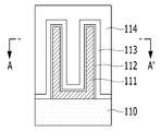
도 1a를 참조하면, 반도체장치(100)는 하부 구조물(110) 및 캐패시터(120)를 포함할 수 있다. 캐패시터(120)는 하부전극(111), 계면층(112), 유전층(113) 및 상부전극(114)을 포함할 수 있다. 하부전극(111) 상에 계면층(112), 유전층(113) 및 상부전극(114)이 차례로 적층될 수 있다. Referring to FIG. 1A, a
하부전극(bottom electrode, 111)은 고종횡비를 가질 수 있다. 여기서, 종횡비는 폭 대 높이의 비율을 일컫는다. 고종횡비는 1:1 보다 큰 종횡비를 지칭할 수 있다. 예컨대, 하부전극(111)은 1:10 이상의 고종횡비를 가질 수 있다. 하부전극(111)은 실린더 형상일 수 있다. 하부전극(111)은 실린더 형상 외에 필라 형상일 수도 있다. 하부전극(111)은 스토리지노드(storage node)라고 지칭될 수 있다. 하부전극(111)은 금속요소(metal element)를 포함하는 금속-베이스 물질을 포함할 수 있다. 예를 들어, 하부전극(111)은 티타늄질화물(TiN), 탄탈륨질화물(TaN) 또는 이들의 조합을 포함할 수 있다. 위와 같이, 하부전극(111)은 금속요소(metal element)와 질소를 포함하는 금속질화물을 포함할 수 있다. 하부전극(111)은 화학양론적 조성비를 갖는 금속질화물일 수 있다. 예컨대, 금속요소와 질소의 조성비가 1:1일 수 있다. 본 실시예에서 하부전극(111)은 티타늄질화물 또는 탄탈륨질화물을 포함할 수 있다. 하부전극(111)은 원자층증착에 의해 형성된 티타늄질화물(ALD-TiN)을 포함할 수 있다. 하부전극(111)은 하부(lower portion, 111L) 및 상부(upper portion, 111U)를 포함할 수 있다. 여기서, 하부(111L)와 상부(111U)는 설명의 편의를 위해 구분한 것으로서, 하부(111L)와 상부(111U)의 높이는 동일하거나 서로 다를 수 있다. 이하, 하부(111L)는 하부 하부전극(Lower bottom electrode, 111L)이라고 지칭하고, 상부(111U)는 상부 하부전극(Upper bottom electrode, 111U)이라고 지칭하기로 한다.The
하부전극(111) 상에 계면층(112)이 형성될 수 있다. 계면층(112)은 하부전극(111)에 함유된 금속요소를 포함할 수 있다. 예를 들어, 계면층(112)은 금속요소의 산화물일 수 있다. 계면층(112)은 하부전극(111)의 표면을 산화시킨 산화물일 수 있다. 계면층(112)은 금속요소와 산소를 포함하는 금속산화물일 수 있다. 계면층(112)과 하부전극(111)은 동일한 금속요소가 함유되어 있을 수 있다. 하부전극(111)이 티타늄질화물인 경우, 계면층(112)은 티타늄산화물일 수 있다. 하부전극(111)이 탄탈륨질화물인 경우, 계면층(112)은 탄탈륨산화물일 수 있다.An
계면층(112)은 하부전극(111)의 표면을 적어도 2회의 플라즈마처리에 노출시켜 형성할 수 있다. 플라즈마처리들에 의해 계면층(112)은 균일한 두께를 가질 수 있다. 고종횡비의 하부전극(111) 상에 균일한 두께를 갖고 계면층(112)이 형성될 수 있다. 계면층(112)은 하부전극(111)의 위치에 따라 제1계면층(112U) 및 제2계면층(112L)을 포함할 수 있다. 제1계면층(112U)은 상부 하부전극(111U) 상에 형성될 수 있다. 제2계면층(112L)은 하부 하부전극(111L) 상에 형성될 수 있다. 복수의 플라즈마처리에 의해 형성된 제1계면층(112U) 및 제2계면층(112L)은 두께가 동일할 수 있다. 제1계면층(112U)은 제1두께(D1)를 갖고, 제2계면층(112L)은 제2두께(D2)를 가질 수 있다. 제1두께(D1)와 제2두께(D2)는 동일할 수 있다. 복수의 플라즈마처리는 플라즈마질화 및 플라즈마산화를 순차적으로 진행할 수 있다. 예컨대, 플라즈마질화및 플라즈마산화에 의해 제1계면층(112U)이 형성될 수 있고, 플라즈마산화에 의해 제2계면층(112L)이 형성될 수 있다. 계면층(112)의 형성 방법은 후술하기로 한다.The
계면층(112) 상에 유전층(113)이 형성될 수 있다. 유전층(113)은 실리콘산화물보다 유전율이 높은 고유전율 물질을 포함할 수 있다. 고유전율 물질(High-k material)은 하프늄산화물(HfO2), 지르코늄산화물(ZrO2), 알루미늄산화물(Al2O3), 티타늄산화물(TiO2), 탄탈륨산화물(Ta2O5), 니오븀산화물(Nb2O5) 또는 스트론튬티타늄산화물(SrTiO3)을 포함할 수 있다. 다른 실시예에서, 유전층(113)은 앞서 언급된 고유전율 물질을 두 층 이상 포함하는 복합층으로 이루어질 수도 있다.A
유전층(113) 상에 상부전극(Top electrode, 114)이 형성될 수 있다. 상부전극(114)은 금속-베이스 물질을 포함할 수 있다. 예를 들어, 상부전극(114)은 티타늄(Ti), 티타늄질화물(TiN), 탄탈륨(Ta), 탄탈륨질화물(TaN), 티타늄알루미늄질화물(TiAlN), 텅스텐(W), 텅스텐질화물(WN), 루테늄(Ru), 루테늄산화물(RuO2), 이리듐(Ir), 이리듐산화물(IrO2), 플래티늄(Pt) 또는 이들의 조합을 포함할 수 있다. 본 실시예에서 상부전극(114)은 원자층증착에 의해 형성된 티타늄질화물(ALD-TiN)을 포함할 수 있다. 상부전극(114)은 하부전극(111)과 동일 재질의 물질을 포함할 수도 있다. A
다른 실시예에서, 상부전극(114)은 다층 구조일 수 있다. 상부전극(114)은 제1금속함유층, 실리콘저마늄층 및 제2금속함유층을 차례로 적층하여 형성할 수도 있다. 제1금속함유층과 제2금속함유층은 티타늄(Ti), 티타늄질화물(TiN), 탄탈륨(Ta), 탄탈륨질화물(TaN), 티타늄알루미늄질화물(TiAlN), 텅스텐(W), 텅스텐질화물(WN), 루테늄(Ru), 루테늄산화물(RuO2), 이리듐(Ir), 이리듐산화물(IrO2), 플래티늄(Pt) 또는 이들의 조합을 포함할 수 있다. 예를 들어, 제1금속함유층은, 티타늄질화물일 수 있고, 제2금속함유층은 텅스텐질화물과 텅스텐이 적층된 WN/W일 수 있다. 실리콘저마늄층은 보론이 도핑될 수 있다.In another embodiment, the
본 실시예에서 유전층(113)은 등가산화막두께(equivalent-oxide thickness; EOT)를 충분히 낮추면서도 양호한 누설 전류 특성을 갖는 지르코늄산화물-베이스 물질로 형성될 수 있다. 예를 들어, ZAZ(ZrO2/Al2O3/ZrO2)를 포함할 수 있다. 다른 실시예에서, 유전층(113)은 HAH(HfO2/Al2O3/HfO2) 를 포함할 수도 있다. In this embodiment, the
도 1b 및 도 1c는 제1실시예의 변형예를 도시한 도면이다.1B and 1C are views showing a modification of the first embodiment.
도 1b를 참조하면, 계면층(112)이 티타늄산화물(TiO2)을 포함하고, 유전층(113)이 ZAZ를 포함하는 경우, 하부전극(111) 상에 TZAZ(TiO2/ZrO2/Al2O3/ZrO2)로 이루어진 유전층 스택이 형성될 수 있다. Referring to FIG. 1B, when the
도 1c를 참조하면, 계면층(112)이 티타늄산화물(TiO2)을 포함하고, 유전층(113)이 HAH를 포함하는 경우, 하부전극(111) 상에 THAH(TiO2/HfO2/Al2O3/HfO2)로 이루어진 유전층 스택이 형성될 수 있다. Referring to FIG. 1C, when the
이와 같은 계면층(112) 및 유전층(113)의 스택에 의해 캐패시턴스를 증가시킬 수 있다. 계면층(112)에 의해 유전층(113)의 산소 손실을 억제하여 캐패시턴스를 더욱 증가시킬 수 있다.The capacitance can be increased by the stack of the
도 1d 및 도 1e는 제1실시예의 다른 변형예를 도시한 도면이다. 도 1d 및 도 1e에서 하부전극(111')과 상부전극(114')은 탄탈륨질화물(TaN)을 포함할 수 있다. 다른 실시예에서, 하부전극(111')은 탄탈륨질화물(TaN)을 포함할 수 있고, 상부전극(114')은 티타늄질화물(TiN)을 포함할 수 있다. 계면층(112')은 탄탈륨산화물(Ta2O5)을 포함할 수 있다.Figs. 1D and 1E are views showing another modification of the first embodiment. In FIGS. 1D and 1E, the lower electrode 111 'and the upper electrode 114' may comprise tantalum nitride (TaN). In another embodiment, the lower electrode 111 'may comprise tantalum nitride (TaN) and the upper electrode 114' may comprise titanium nitride (TiN). The interface layer 112 'may comprise tantalum oxide (Ta 2 O 5 ).
도 1d를 참조하면, 계면층(112')이 탄탈륨산화물(Ta2O5)을 포함하고, 유전층(113)이 ZAZ를 포함하는 경우, 하부전극(111') 상에 TZAZ(Ta2O5/ZrO2/Al2O3/ZrO2)로 이루어진 유전층 스택이 형성될 수 있다. Referring to FIG. 1D, when the interfacial layer 112 'includes tantalum oxide (Ta 2 O 5 ) and the
도 1e를 참조하면, 계면층(112')이 탄탈륨산화물(Ta2O5)을 포함하고, 유전층(113)이 HAH를 포함하는 경우, 하부전극(111) 상에 THAH(Ta2O5/HfO2/Al2O3/HfO2)로 이루어진 유전층 스택이 형성될 수 있다. Referring to FIG. 1E, when the interfacial layer 112 'includes tantalum oxide (Ta 2 O 5 ) and the
도 2a 내지 도 2e는 도 1a의 계면층(112)을 형성하는 방법의 일예를 설명하기 위한 도면이다.2A to 2E are views for explaining an example of a method of forming the
도 2a에 도시된 바와 같이, 하부 구조물(110) 상에 하부전극(111)이 형성될 수 있다. 하부전극(111)은 티타늄질화물을 포함할 수 있다. As shown in FIG. 2A, the
하부전극(111)은 제1플라즈마처리(131)에 노출될 수 있다. 제1플라즈마처리(131)는 저압(Low pressure)에서 수행될 수 있다. 제1플라즈마처리(131)가 저압에서 수행됨에 따라, 많은 양의 질소이온플라즈마(131N)를 형성시킬 수 있다. 이때, 질소이온플라즈마(131N)의 효율을 높이기 위하여, 첨가가스를 추가할 수 있다. 첨가가스는 Ar 또는 He을 포함할 수 있다. The
제1플라즈마처리(131)는 저압 플라즈마질화(low pressure plasma nitridation; LPPN)를 포함할 수 있다. 제1플라즈마처리(131)는 저압에서 질소함유가스분위기로 수행될 수 있다. 예를 들어, 100mTorr 이하의 압력에서 N2 또는 NH3 가스를 사용할 수 있다. The
본 실시예에서, 제1플라즈마처리(131)가 질소분위기의 저압에서 수행되는 경우, 높은 반응력을 갖는 질소이온플라즈마(131N)는 하부전극(111)의 상부에 포격(Bombardment, 131B)될 수 있다. 이와 같이, 제1플라즈마처리(131)는 질소이온플라즈마(131N)가 지배적인 분위기의 저압에서 수행될 수 있다.In the present embodiment, when the
이러한 제1플라즈마처리(131)의 결과로써, 도 2b에 도시된 질소리치층(Nitrogen-rich layer, 132)이 형성될 수 있다. 예를 들어, 하부전극(111)이 티타늄질화물인 경우, 질소리치층(132)은 질소리치 티타늄질화물(N rich TixNy)을 포함할 수 있다. 하부전극(111)의 상부가 완전히 질소리치층(132)으로 변환되지 않을 수 있다. 하부전극(111)은 하부 하부전극(111L) 및 상부 하부전극(111U)을 포함할 수 있다. 상부 하부전극(111U)은 질소리치층(132)과 비-플라즈마처리부(132N)를 포함할 수 있다. 비-플라즈마처리부(132N)는 상부 하부전극(111U)의 내부로 정의될 수 있고, 질소리치층(132)은 상부 하부전극(111U)의 표면으로 정의될 수 있다. 질소리치층(132)은 비-플라즈마처리부(132N)를 커버링하는 형상일 수 있다. 하부 하부전극(111L)은 비-플라즈마처리될 수 있다. 즉, 하부 하부전극(111L)은 질소리치층(132)을 포함하지 않을 수 있다.As a result of the
제1플라즈마처리(131)에 의해 상부 하부전극(111U)에 국부적으로 질소리치층(132)을 형성할 수 있다. 질소리치층(132)에 의해 하부전극(111)은 불균일한 질소 프로파일을 갖게 된다. 하부 하부전극(111L)은 티타늄질화물로 잔류할 수 있고, 상부 하부전극(111U)은 티타늄질화물과 질소리치 티타늄질화물이 혼재될 수 있다. 따라서, 하부 하부전극(111L)은 화학양론적조성의 티타늄질화물일 수 있고, 상부 하부전극(111U)은 질소리치 티타늄질화물일 수 있다.The
위와 같이, 상부 하부전극(111U)과 하부 하부전극(111L)은 서로 다른 질소함량을 갖는 티타늄질화물로 형성될 수 있다. 하부 하부전극(111L)은 '화학양론적조성(Stoichiometric ratio)을 갖는 티타늄질화물'로 형성되고, 상부 하부전극(111)은 '질소 리치 티타늄질화물'로 형성될 수 있다.As described above, the upper
도 2c에 도시된 바와 같이, 질소리치층(132)이 형성된 하부전극(111)은 제2플라즈마처리(133)에 노출될 수 있다. 제2플라즈마처리(133)는 제1플라즈마처리(131)보다 높은 압력에서 수행될 수 있다. 예를 들어, 제2플라즈마처리(132)는 1torr보다 높은 압력에서 수행될 수 있다. 제2플라즈마처리(132)는 산소 분위기에서 수행될 수 있다. 제2플라즈마처리(133)는 고압플라즈마산화(High Pressure Plsma Oxidation, HPPO)를 포함할 수 있다.2C, the
높은 압력에서는 산소이온플라즈마가 쉽게 에너지를 잃어버린다. 따라서, 산소이온플라즈마(133I)의 양이 감소하게 되고, 산소라디칼플라즈마(133R)가 지배적으로 존재하게 된다. 산소라디칼플라즈마(133R)는 산소이온플라즈마(133I)와 달리 중성종으로서, 균일한 산화에 유리하다. 이와 같이, 제2플라즈마처리(133)는 산소라디칼플라즈마(133R)가 지배적인 분위기의 고압에서 수행될 수 있다.At higher pressures, the oxygen ion plasma easily loses energy. Accordingly, the amount of the oxygen ion plasma 133I is reduced, and the oxygen
그럼에도 불구하고, 반응성이 높은 산소이온플라즈마(133I)가 여전히 소량 존재할 수 있다. 산소플라즈마 입자들이 상부 하부전극(111U)에 주입되므로 여전히 하부 하부전극(111L) 대비 상부에 산소 플라즈마입자들이 많은 시간 접촉하게 된다.Nevertheless, there may still be a small amount of highly reactive oxygen ion plasma 133I. The oxygen plasma particles are injected into the upper
질소리치층(132)이 상부 하부전극(111U)에 미리 존재하고 있으므로, 상부 하부전극(111U)에서는 산화가 아닌, 환원이 먼저 발생하게 된다. 즉, 질소리치층(132)의 질소(133N)가 산소로 치환되어 TiN 산화가 지연된다. 지연되는 시간 동안 산소라디칼플라즈마(133R')가 하부 하부전극(111L) 및 바닥까지 도달한다. Since the nitrogen-
제2플라즈마처리(133)에 의해, 도 2d에 도시된 바와 같이, 상부 하부전극(111U) 상에 제1계면층(112U)이 형성될 수 있고, 하부 하부전극(111L) 상에 제2계면층(112L)이 형성될 수 있다. 상부 하부전극(111U)에서는 질소 환원 반응/산소 치환 반응(133A)에 의해 제1계면층(112U)이 형성될 수 있다. 하부 하부전극(111L)에서는 산화 반응(133B)에 의해 제2계면층(112L)이 형성된다. 제1계면층(112U)은 제1두께(D1)를 갖고, 제2계면층(112L)은 제2두께(D2)를 가질 수 있다. 제1두께(D1)와 제2두께(D2)는 동일할 수 있다. The
제1계면층(112U) 및 제2계면층(112L)은 다음과 같은 원리에 의해 형성될 수 있다. 하부전극(111)이 티타늄질화물(TiN)인 경우를 예로 들어 설명한다. 상부 하부전극(111U)에서는 질소리치층(132), 즉 질소리치티타늄질화물(N rich TixNy)의 질소(Nitrogen)가 산소(oxygen)로 치환된다. 이에 따라, 질소리치층(132)이 감소되면서 제1계면층(112U)으로서 티타늄산화물(TiO2)이 형성된다. 하부 하부전극(111L)에서는 산화 반응(133B)에 의해 티타늄질화물이 산화되어 제2계면층(112L)으로서 티타늄산화물(TiO2)이 형성된다.The
위와 같은 일련의 저압의 제1플라즈마처리(131) 및 고압의 제2플라즈마처리(133)를 순차적으로 수행하므로써, 하부전극(111)의 표면에 균일한 두께의 계면층(112)이 형성될 수 있다. 계면층(112)은 제1계면층(112U)과 제2계면층(112L)을 포함할 수 있다. 제1 및 제2계면층(112U, 112L)은 산화물을 포함할 수 있다. 제1 및 제2계면층(112U, 112L)은 하부전극(111)의 금속요소를 포함하는 산화물일 수 있다. 하부전극(111)이 티타늄질화물일 경우, 제1 및 제2계면층(112U, 112L)은 티타늄산화물(TiO2)을 포함할 수 있다. The
도 3a는 표면 질화 및 표면 산화된 TiN 표면의 화학적상태(chemical state)를 분석한 XPS 결과이다. FIG. 3A shows the XPS results of analyzing the chemical state of the surface nitrided and surface oxidized TiN surface.
플라즈마질화(PN) 후에는 다양한 비화학양론(Non-stoichiometry) 성분들이 존재할 수 있다. 비화학양론 성분들은 TiOxNy, TiOx, Ti2O3, TiNx 등을 포함할 수 있다. 이에 반해, 플라즈마산화(PO)를 적용하면 서브 상(sub-phase)이 감소하고 TiO2 성분이 증가하는 것을 알 수 있다. 즉, 질소(Nitrogen)가 산소(Oxygen)로 치환되면서 막질이 우수한 TiO2 상태가 형성된다. 이러한 치환반응은 열역학적으로 Ti-O 결합이 Ti-N 결합보다 깁스 프리 에너지(│△G│)가 크기 때문이다.After plasma nitridation (PN), various non-stoichiometric components may be present. The non-stoichiometric components may include TiO x N y , TiO x , Ti 2 O 3 , TiN x , and the like. On the contrary, when the plasma oxidation (PO) is applied, the sub-phase decreases and the TiO 2 component increases. That is, the nitrogen oxide is replaced with oxygen to form a TiO 2 state excellent in film quality. This substitution reaction is thermodynamically because the Ti-O bond has a larger Gibbs free energy (│ΔG│) than the Ti-N bond.
도 2e에 도시된 바와 같이, 균일한 계면층(112)이 형성된 하부전극(111) 상에 유전층(113) 및 상부전극(114)을 형성한다. The
도 3b는 도 2e의 A-A' 방향에 따른 TEM 사진으로서, 하부전극(111)의 표면 상에 얇고 균일한 계면층(112)이 형성됨을 알 수 있다.FIG. 3B is a TEM image taken along a line A-A 'in FIG. 2E, which shows that a thin and
계면층(112)의 두께가 두꺼울 경우, 전체 캐패시턴스를 오히려 감소시킬 수 있다. 따라서, 계면층(112)은 2nm 이하의 얇은 두께로 형성될 수 있다. 계면층(112)의 얇은 두께 제어를 위해, 열산화(thermal oxidation)보다 플라즈마산화가 유리하다. 또한, 하부전극(111)의 상부 및 하부에서 계면층(112)을 균일한 두께로 형성하기 위해, 저압플라즈마질화 및 고압플라즈마산화를 순차적으로 실시한다.If the thickness of the
도 4a 내지 도 4c는 플라즈마산화를 단독으로 수행하는 비교예를 설명하기 위한 도면이다.4A to 4C are diagrams for explaining a comparative example in which plasma oxidation is performed alone.
도 4a에 도시된 바와 같이, 하부전극(111) 및 유전층(113)이 형성될 수 있다. 하부전극(111)은 티타늄질화물을 포함할 수 있고, 유전층(113)은 지르코늄산화물(ZrO2)을 포함할 수 있다. As shown in FIG. 4A, the
하부전극(111)의 표면에는 복수의 표면 결함(surface defect)이 존재할 수 있다. 즉, 유전층(113)의 산소를 빼앗는 결함들이 존재할 수 있다. A plurality of surface defects may exist on the surface of the
하부전극(111)은 주상구조일 수 있다. 따라서, 하부전극(111)은 복수의 결정립계(grain boundary, GB)를 포함할 수 있다. 하부전극(111)으로 적용된 티타늄질화물(TiN)은 높은 결정성을 가지며, 주상구조(columnar structure)로 성장될 수 있다. 주상구조의 티타늄질화물은 불안정한 상태의 많은 결정립계(GB), 즉 TiNx를 가질 수 있다. 이에 따라, 표면 에너지가 높기 때문에 후속 유전층(113)의 산소를 뺏어올 수 있다. The
하부전극(111)의 표면에 존재하는 자연산화물(TiOxNy)또한 다량의 산소공공(Oxygen vacancy, Vo)을 가지고 있고, 이에 따라 유전층(113)의 산소를 뺏어오게 된다(도면부호 '113A' 참조). The natural oxide (TiO x N y ) existing on the surface of the
하부전극(111)과 유전층(113) 사이의 계면에는 비화학양론적 화합물(non-stoichiometry compoung)이 존재할 수 있다. 예컨대, TiOxNy, TiOx, TiNx 등이 존재할 수 있다. 비화학양론적 화합물은 산소를 끌어당기는 힘이 매우 크기 때문에, 유전층(113)의 산소 손실을 초래한다.A non-stoichiometric compound may be present at the interface between the
위와 같은 유전층(113)의 산소 손실은 기생 캐패시턴스(113B)를 초래할 수 있다. 예를 들어, ZrOx 및 TiOx의 기생캐패시턴스(113B)를 유발한다. 결국, 유전층(113)의 캐패시턴스(capacitance)를 낮게 하고, 누설전류를 증가시킬 수 있다. The oxygen loss of the
따라서, 유전층(113)의 산소 손실을 억제하기 위해 하부전극(111)의 표면을 산화시키는 방법이 필요하다. 하부전극(111)의 표면을 과도하게 산화시킬 경우, 두꺼운 산화물이 형성되어, 캐패시턴스가 감소하게 되므로 얇은 두께의 제어가 중요하다.Therefore, a method of oxidizing the surface of the
도 4b에 도시된 바와 같이, 플라즈마산화(Plasma oxidation)를 단독으로 수행하는 경우, 하부전극(111)의 표면 결함을 제거하여 유전층(113)의 산소손실을 억제할 수 있다.As shown in FIG. 4B, when plasma oxidation is performed alone, surface defects of the
예를 들어, 티타늄질화물(TiN)의 결정립계에 산소가 미리 자리를 잡아 안정적인 TiON이 형성될 수 있고(TiNx→TiON), 티타늄질화물 표면에는 질소를 치환하면서 TiO2이 형성될 수 있다(TiOx→TiO2). For example, TiO 2 can be formed by substituting oxygen for the grain boundaries of titanium nitride (TiN) to form stable TiON (TiN x → TiON) and replacing nitrogen on the surface of titanium nitride (TiO x → TiO 2 ).
위와 같이, 플라즈마산화에 의해, 하부전극(111)의 표면에 계면층(112T)이 형성될 수 있다. 결국, 플라즈마산화에 의해 ZrOx 및 TiOx 형성이 억제되어, 전체 캐패시턴스가 증가하고, 누설전류 또한 감소할 수 있다. As described above, the
그러나, 플라즈마산화를 단독으로 수행하는 경우에는, 하부전극(111)의 상부와 하부에서 균일한 두께의 계면층(112T)을 형성하기 어렵다.However, in the case of performing plasma oxidation alone, it is difficult to form the
DRAM의 스케일링(scaling)이 지속화됨에 따라, 캐패시터를 형성하는 공정의 난이도가 급격히 높아지고 있다. 구체적으로 하부전극(111)의 종횡비가 증가하고, 소스가스가 유입되는 주입구가 협소해져 상부 하부전극(111U)과 하부 하부전극(111L)의 균일한 상태를 유지하는 것이 어렵다. As the scaling of the DRAM continues, the complexity of the process of forming the capacitor is rapidly increasing. Specifically, the aspect ratio of the
도 4c에 도시된 바와 같이, 플라즈마산화를 통해 표면 산화를 진행할 경우, 상부 하부전극(111U) 상에는 두꺼운 산화물(D1')이 형성되고, 하부 하부전극(111L)은 산화가 잘되지 않아 얇은 두께의 산화물(D2')이 형성된다. As shown in FIG. 4C, when surface oxidation is performed through plasma oxidation, a thick oxide D1 'is formed on the upper
위와 같이 산화물의 두께 불균일로 인해, 캐패시턴스가 오히려 감소할 수 있다. 아울러, 상부 하부전극(111U) 상에 형성된 두꺼운 산화물(D1')로 인해 하부전극(111)이 붕괴되는 문제가 발생할 수 있다.Due to the thickness unevenness of the oxide as described above, the capacitance can be rather reduced. In addition, a problem may occur that the
비교예와는 다르게, 도 2a 내지 도 2e에 도시된 것처럼, 본 실시예는 저압의 플라즈마질화 및 고압의 플라즈마산화를 조합하므로써, 고종횡비의 하부전극(111) 표면에 균일하게 계면층(112)을 형성할 수 있다. 계면층(112)에 의해 캐패시턴스 향상 및 낮은 누설 전류, 그리고 우수한 신뢰성의 캐패시터를 형성할 수 있다.2A to 2E, the present embodiment combines the low-pressure plasma nitridation and the high-pressure plasma oxidation to uniformly form the
또다른 비교예로서, 플라즈마질화를 단독으로 수행할 수 있다. 이 경우에는, 유전층(113)의 산소 손실을 억제하기 어렵다.As another comparative example, plasma nitridation can be performed alone. In this case, it is difficult to suppress the oxygen loss of the
도 1d 및 도 1e에 도시된 하부전극(111')은 탄탈륨질화물(TaN)을 포함할 수 있다. 탄탈륨질화물은 티타늄질화물 대비 일함수가 높아 누설전류에 유리하다. 또한, 막밀도가 높아 안정된 구조를 형성할 수 있다. 하부전극(111')이 탄탈륨질화물일 경우, 계면층(112')은 탄탈륨산화물(Ta2O5)을 포함할 수 있다.The lower electrode 111 'shown in FIGS. 1D and 1E may comprise tantalum nitride (TaN). Tantalum nitride has a higher work function than titanium nitride, which is advantageous for leakage current. Further, the film density is high and a stable structure can be formed. When the lower electrode 111 'is tantalum nitride, the interface layer 112' may include tantalum oxide (Ta 2 O 5 ).
도 5는 탄탈륨질화물 하부전극의 표면에 탄탈륨산화물을 형성하기 위한 방법을 설명하기 위한 도면이다.5 is a view for explaining a method for forming tantalum oxide on the surface of a tantalum nitride lower electrode.
도 5를 참조하면, 탄탈륨질화물 하부전극(111')은 도 2a의 저압의 제1플라즈마처리(131)에 노출될 수 있다. 이로써, 탄탈륨질화물 하부전극(111')의 상부(111U')에 국부적으로 질소리치층(132')을 형성할 수 있다. 질소리치층(132')은 질소 리치 탄탈륨질화물(N rich TaxNy)일 수 있다.Referring to FIG. 5, the tantalum nitride lower electrode 111 'may be exposed to the low pressure
질소리치층(132')이 형성된 탄탈륨질화물 하부전극(111')은 도 2c의 고압의 제2플라즈마처리(133)에 노출될 수 있다. 이로써, 탄탈륨질화물 하부전극(111')의 상부(111U') 상에 제1계면층(112U')이 형성될 수 있고, 탄탈륨질화물 하부전극(111')의 하부(111L') 상에 제2계면층(112L')이 형성될 수 있다. 탄탈륨질화물 하부전극(111')의 상부(111U')에서는 질소 환원 반응/산소 치환 반응(133A)에 의해 제1계면층(112U')이 형성될 수 있다. 탄탈륨질화물 하부전극(111')의 하부(111L')에서는 산화 반응(133B)에 의해 제2계면층(112L')이 형성될 수 있다. 제1계면층(112U') 및 제2계면층(112L')은 동일한 두께를 가질 수 있다. 제1계면층(112U') 및 제2계면층(112L')은 탄탈륨산화물(Ta2O5)일 수 있다. 제1계면층(112U') 및 제2계면층(112L')이 형성되는 원리는 도 2c 및 그에 따른 설명을 참조하기로 한다.The tantalum nitride lower electrode 111 'in which the nitrogen rich layer 132' is formed may be exposed to the high-pressure
도 6은 제2실시예에 따른 반도체장치를 도시한 도면이다.6 is a view showing a semiconductor device according to the second embodiment.
도 6을 참조하면, 반도체장치(100M)는 하부 구조물(110) 및 캐패시터(120P)를 포함할 수 있다. 캐패시터(120P)는 하부전극(111P), 계면층(112P), 유전층(113) 및 상부전극(114)을 포함할 수 있다. 하부전극(111P) 상에 계면층(112P), 유전층(113) 및 상부전극(114)이 차례로 적층될 수 있다. Referring to FIG. 6, the
하부전극(111P)은 고종횡비를 가질 수 있다. 여기서, 고종횡비는 폭 대 높이의 비율을 일컫는다. 하부전극(111)은 1:1 보다 큰 종횡비를 지칭할 수 있다. 예컨대, 하부전극(111P)은 1:10 이상의 종횡비를 가질 수 있다. 하부전극(111P)은 필라 형상일 수 있다. 하부전극(111P)은 스토리지노드(storage node)라고 지칭될 수 있다. 하부전극(111P)은 금속요소(metal element)를 포함하는 금속-베이스 물질을 포함할 수 있다. 예를 들어, 하부전극(111P)은 티타늄질화물(TiN), 탄탈륨질화물(TaN) 또는 이들의 조합을 포함할 수 있다. 위와 같이, 하부전극(111P)은 금속요소와 질소를 포함하는 금속질화물을 포함할 수 있다. 하부전극(111P)은 화학양론적 조성비를 갖는 금속질화물일 수 있다. 즉, 금속과 질소의 조성비가 1:1일 수 있다. 본 실시예에서 하부전극(111P)은 티타늄질화물 또는 탄탈륨질화물을 포함할 수 있다. 하부전극(111P)은 원자층증착에 의해 형성된 티타늄질화물(ALD-TiN)을 포함할 수 있다. 하부전극(111P)은 하부 하부전극(111L) 및 상부 하부전극(111U)을 포함할 수 있다.The
하부전극(111P) 상에 계면층(112P)이 형성될 수 있다. 계면층(112P)은 하부전극(111P)에 함유된 금속요소를 포함할 수 있다. 예를 들어, 계면층(112P)은 금속요소의 산화물일 수 있다. 계면층(112P)은 하부전극(111P)의 산화물일 수 있다. 계면층(112P)은 금속요소와 산소를 포함하는 금속산화물일 수 있다. 계면층(112P)과 하부전극(111P)은 동일한 금속요소가 함유되어 있을 수 있다. 하부전극(111P)이 티타늄질화물인 경우, 계면층(112P)은 티타늄산화물일 수 있다. 하부전극(111P)이 탄탈륨질화물인 경우, 계면층(112P)은 탄탈륨산화물일 수 있다.An
계면층(112P)은 도 2a 및 도 2c에 도시된 바와 같은 2회의 플라즈마처리에 의해 형성될 수 있다. 플라즈마처리에 의해 계면층(112P)은 균일한 두께를 가질 수 있다. 고종횡비의 하부전극(111P) 상에 균일한 두께를 갖고 계면층(112P)이 형성될 수 있다. 계면층(112P)은 하부전극(111P)의 위치에 따라 제1계면층(112U) 및 제2계면층(112L)을 포함할 수 있다. 제1계면층(112U)은 상부 하부전극(111U) 상에 형성될 수 있다. 제2계면층(112L)은 하부 하부전극(111L) 상에 형성될 수 있다. 복수의 플라즈마처리에 의해 형성된 제1계면층(112U) 및 제2계면층(112L)은 두께가 동일할 수 있다. 제1계면층(112U)은 제1두께(D11)를 갖고, 제2계면층(112L)은 제2두께(D12)를 가질 수 있다. 제1두께(D11)와 제2두께(D12)는 동일할 수 있다. 복수의 플라즈마처리는 플라즈마질화 및 플라즈마산화를 순차적으로 진행할 수 있다.The
계면층(112P) 상에 유전층(113)이 형성될 수 있다. 유전층(113)은 실리콘산화물보다 유전율이 높은 고유전율 물질을 포함할 수 있다. 고유전율 물질(High-k material)은 하프늄산화물(HfO2), 지르코늄산화물(ZrO2), 알루미늄산화물(Al2O3), 티타늄산화물(TiO2), 탄탈륨산화물(Ta2O5), 니오븀산화물(Nb2O5) 또는 스트론튬티타늄산화물(SrTiO3)을 포함할 수 있다. 다른 실시예에서, 유전층(113)은 앞서 언급된 고유전율 물질을 두 층 이상 포함하는 복합층으로 이루어질 수도 있다.The
유전층(113) 상에 상부전극(114)이 형성될 수 있다. 상부전극(114)은 금속-베이스 물질을 포함할 수 있다. 예를 들어, 상부전극(114)은 티타늄(Ti), 티타늄질화물(TiN), 탄탈륨(Ta), 탄탈륨질화물(TaN), 티타늄알루미늄질화물(TiAlN), 텅스텐(W), 텅스텐질화물(WN), 루테늄(Ru), 루테늄산화물(RuO2), 이리듐(Ir), 이리듐산화물(IrO2), 플래티늄(Pt) 또는 이들의 조합을 포함할 수 있다. 본 실시예에서 상부전극(114)은 원자층증착에 의해 형성된 티타늄질화물(ALD-TiN)을 포함할 수 있다.상부전극(114)은 하부전극(111P)과 동일 재질의 물질을 포함할 수도 있다. An
다른 실시예에서, 상부전극(114)은 다층 구조일 수 있다. 상부전극(114)은 제1금속함유층, 실리콘저마늄층 및 제2금속함유층을 차례로 적층하여 형성할 수도 있다. 제1금속함유층과 제2금속함유층은 티타늄(Ti), 티타늄질화물(TiN), 탄탈륨(Ta), 탄탈륨질화물(TaN), 티타늄알루미늄질화물(TiAlN), 텅스텐(W), 텅스텐질화물(WN), 루테늄(Ru), 루테늄산화물(RuO2), 이리듐(Ir), 이리듐산화물(IrO2), 플래티늄(Pt) 또는 이들의 조합을 포함할 수 있다. 예를 들어, 제1금속함유층은, 티타늄질화물일 수 있고, 제2금속함유층은 텅스텐질화물과 텅스텐이 적층된 WN/W일 수 있다. 실리콘저마늄층은 보론이 도핑될 수 있다.In another embodiment, the
본 실시예에서 유전층(113)은 등가산화막두께(EOT)를 충분히 낮추면서도 양호한 누설 전류 특성을 갖는 지르코늄산화물-베이스 물질로 형성될 수 있다. 예를 들어, ZAZ(ZrO2/Al2O3/ZrO2)를 포함할 수 있다. 다른 실시예에서, 유전층(113)은 HAH(HfO2/Al2O3/HfO2) 를 포함할 수도 있다. In this embodiment, the
유전층(113)은 도 1b 내지 도 1e에 도시된 다층 유전층을 포함할 수도 있다.The
도 7a 내지 도 7d는 도 6의 계면층을 형성하는 방법의 일예를 설명하기 위한 도면이다.7A to 7D are views for explaining an example of a method of forming the interface layer of FIG.
도 7a에 도시된 바와 같이, 하부 구조물(110) 상에 하부전극(111P)이 형성될 수 있다. 하부전극(111P)은 티타늄질화물을 포함할 수 있다. 하부전극(111P)은 주상구조일 수 있다. 하부전극(111P)은 필라 형상일 수 있다.As shown in FIG. 7A, the
도 7b에 도시된 바와 같이, 하부전극(111P)은 제1플라즈마처리(131P)에 노출될 수 있다. 제1플라즈마처리(131P)는 도 2a의 제1플라즈마처리(131)와 동일하게 수행될 수 있다. 제1플라즈마처리(131P)는 저압에서 수행될 수 있다. 제1플라즈마처리(131P)는 저압 플라즈마질화(LPPN)를 포함할 수 있다. 제1플라즈마처리(131P)는 저압에서 질소함유가스분위기로 수행될 수 있다. 예를 들어, 100mTorr 이하의 압력에서 N2 또는 NH3 가스를 사용할 수 있다. As shown in FIG. 7B, the
본 실시예에서, 제1플라즈마처리(131P)가 질소분위기의 저압에서 수행되는 경우, 질소리치층(132P)이 형성될 수 있다. 예를 들어, 하부전극(111P)이 티타늄질화물인 경우, 질소리치층(132P)은 질소리치 티타늄질화물(N rich TixNy)을 포함할 수 있다. 하부전극(111P)의 상부가 완전히 질소리치층(132P)으로 변환되지 않을 수 있다. 하부전극(111P)은 하부 하부전극(111L) 및 상부 하부전극(111U)을 포함할 수 있다. 상부 하부전극(111U)는 질소리치층(132P)과 비-플라즈마처리부(132N)를 포함할 수 있다. 비-플라즈마처리부(132N)는 상부 하부전극(111U)의 내부로 정의될 수 있고, 질소리치층(132P)은 상부 하부전극(111U)의 표면으로 정의될 수 있다. 하부하부전극(111L)은 비-플라즈마처리될 수 있다. 즉, 하부 하부전극(111L)은 질소리치층(132P)을 포함하지 않을 수 있다.In this embodiment, when the
위와 같이, 제1플라즈마처리(131P)에 의해 상부 하부전극(111U)에 국부적으로 질소리치층(132P)을 형성할 수 있다. 질소리치층(132P)에 의해 하부전극(111P)은 불균일한 질소 프로파일을 갖게 된다. 즉, 하부 하부전극(111L)은 티타늄질화물로 잔류할 수 있고, 상부 하부전극(111U)은 티타늄질화물과 질소리치 티타늄질화물이 혼재될 수 있다. 따라서, 상부 하부전극(111U)과 하부 하부전극(111L)은 서로 다른 질소함량을 갖는 티타늄질화물이 될 수 있다.As described above, the nitrogen-
도 7c에 도시된 바와 같이, 질소리치층(132P)이 형성된 하부전극(111P)은 제2플라즈마처리(133P)에 노출될 수 있다. 제2플라즈마처리(133P)는 도 2c의 제2플라즈마처리(133)와 동일하게 수행될 수 있다. 제2플라즈마처리(133P)는 제1플라즈마처리(131P)보다 높은 압력에서 수행될 수 있다. 예를 들어, 제2플라즈마처리(133P)는 1torr보다 높은 압력에서 수행될 수 있다. 제2플라즈마처리(133P)는 산소 분위기에서 수행될 수 있다. 제2플라즈마처리(133P)는 플라즈마산화를 포함할 수 있다.As shown in FIG. 7C, the
제2플라즈마처리(133P)에 의해, 상부 하부전극(111U)에서는 질소 환원 반응 및 산소 치환 반응에 의해 제1계면층(112U)이 형성되고, 하부 하부전극(111L)에서는 산화 반응에 의해 제2계면층(112L)이 형성된다. 제1계면층(112U)과 제2계면층(112L)은 동일한 두께(D11=D12)일 수 있다. The
위와 같은 일련의 저압의 제1플라즈마처리(131P) 및 고압의 제2플라즈마처리(133P)를 순차적으로 수행하므로써, 하부전극(111P)의 표면에 균일한 두께의 계면층(112P)이 형성될 수 있다. 계면층(112P)은 제1계면층(112U)과 제2계면층(112L)을 포함할 수 있다. 제1 및 제2계면층(112U, 112L)은 산화물을 포함할 수 있다. 제1 및 제2계면층(112U, 112L)은 하부전극(111P)의 금속요소를 포함하는 산화물일 수 있다. 하부전극(111P)이 티타늄질화물일 경우, 제1 및 제2계면층(112U, 112L)은 티타늄산화물(TiO2)을 포함할 수 있다. 다른 실시예에서, 하부전극(111P)이 탄탈륨질화물일 경우, 제1 및 제2계면층(112U, 112L)은 탄탈륨산화물(Ta2O5)을 포함할 수 있다. The
도 7d에 도시된 바와 같이, 계면층(112P) 상에 유전층(113) 및 상부전극(114)이 형성될 수 있다.7D, a
다른 실시예로서, 하부 전극(111P)은 탄탈륨질화물(TaN)을 포함할 수 있다. 이 경우, 계면층(112P)은 탄탈륨산화물일 수 있다.In another embodiment, the
도 8a 내지 도 8c는 제3실시예에 따른 반도체장치를 도시한 도면이다. 제3실시예는, DRAM 등과 같은 메모리셀을 갖는 반도체장치에 대해 설명한다. 도 8a는 제3실시예에 따른 반도체장치의 평면도이다. 도 8b는 도 8a의 A-A'선에 따른 단면도이다. 도 8c는 도 8a의 B-B'선에 따른 단면도이다. 8A to 8C are diagrams showing a semiconductor device according to the third embodiment. The third embodiment describes a semiconductor device having a memory cell such as a DRAM or the like. 8A is a plan view of the semiconductor device according to the third embodiment. 8B is a cross-sectional view taken along the line A-A 'in FIG. 8A. 8C is a cross-sectional view taken along the line B-B 'in FIG. 8A.
반도체장치(200)는 복수의 메모리셀을 포함할 수 있다. 각각의 메모리셀은 매립워드라인(205)을 포함하는 셀트랜지스터(T), 비트라인(212) 및 캐패시터(300)를 포함할 수 있다. The
반도체장치(200)를 자세히 살펴보기로 한다.The
기판(201)에 소자분리층(202I) 및 활성영역(202)이 형성될 수 있다. 소자분리층(202I)에 의해 복수의 활성영역(202)이 정의될 수 있다. 기판(201)은 반도체프로세싱에 적합한 물질일 수 있다. 기판(201)은 반도체기판을 포함할 수 있다. 기판(201)은 실리콘을 함유하는 물질로 이루어질 수 있다. 기판(201)은 실리콘, 단결정 실리콘, 폴리실리콘, 비정질 실리콘, 실리콘저마늄, 단결정 실리콘저마늄, 다결정 실리콘저마늄, 탄소 도핑된 실리콘, 그들의 조합 또는 그들의 다층을 포함할 수 있다. 기판(201)은 저마늄과 같은 다른 반도체물질을 포함할 수도 있다. 기판(201)은 Ⅲ/Ⅴ족 반도체기판, 예컨대 GaAs과 같은 화합물반도체기판을 포함할 수도 있다. 기판(201)은 SOI(Silicon On Insulator) 기판을 포함할 수도 있다. 소자분리층(202I)은 STI(Shallow Trench Isolation) 공정에 의해 형성될 수 있다.The device isolation layer 202I and the
기판(201)에 게이트트렌치(203)가 형성될 수 있다. 게이트트렌치(203)의 표면 상에 게이트절연층(204)이 형성된다. 게이트절연층(204) 상에 게이트트렌치(203)를 부분적으로 채우는 매립워드라인(205)이 형성될 수 있다. 매립워드라인(205) 상에 실링층(Sealing layer, 206)이 형성될 수 있다. 실링층(206)은 기판(201)의 표면과 동일한 높이를 가질 수 있다. 매립워드라인(205)은 기판(201)의 표면보다 낮은 레벨일 수 있다. 매립워드라인(205)은 저저항 금속물질일 수 있다. 매립워드라인(205)은 티타늄질화물과 텅스텐이 차례로 적층될 수 있다. 다른 실시예에서, 매립워드라인(205)은 티타늄질화물 단독(TiN Only)으로 형성될 수 있다.The
기판(201)에 제1 및 제2소스/드레인영역(207, 208)이 형성될 수 있다. 제1 및 제2소스/드레인영역(207, 208)은 게이트트렌치(203)에 의해 서로 이격될 수 있다. 이로써, 매립워드라인(205), 제1 및 제2소스/드레인영역(207, 208)은 셀트랜지스터(T)가 될 수 있다. 셀트랜지스터(T)는 매립워드라인(205)에 의해 숏채널효과를 개선할 수 있다. First and second source /
기판(201) 상에 비트라인콘택플러그(209)가 형성될 수 있다. 비트라인콘택플러그(209)는 제1소스/드레인영역(207)에 접속될 수 있다. 비트라인콘택플러그(209)는 비트라인콘택홀(210) 내에 위치할 수 있다. 비트라인콘택홀(210)은 하드마스크층(211)에 형성될 수 있다. 하드마스크층(211)은 기판(201) 상에 형성될 수 있다. 비트라인콘택홀(210)은 제1소스/드레인영역(207)을 노출시킬 수 있다. 비트라인콘택플러그(209)의 하부면은 기판(201)의 상부면보다 낮을 수 있다. 비트라인콘택플러그(209)는 폴리실리콘 또는 금속물질로 형성될 수 있다. 비트라인콘택플러그(209)의 일부는 비트라인콘택홀(210)의 직경보다 더 작은 선폭을 가질 수 있다. 이에 따라, 비트라인콘택플러그(209) 양측에 각각 갭(Gap; G)이 형성될 수 있다. 갭(G)은 비트라인콘택플러그(209)의 양측에 독립적으로 형성된다. 결국, 비트라인콘택홀(210) 내에는 하나의 비트라인콘택플러그(209)와 한 쌍의 갭(G)이 위치하며, 한 쌍의 갭(G)은 비트라인콘택플러그(209)에 의해 분리될 수 있다. 비트라인콘택플러그(209)와 실리콘플러그(216) 사이에 갭(G)이 위치할 수 있다.A bit
비트라인콘택플러그(209) 상에 비트라인구조물(BL)이 형성될 수 있다. 비트라인구조물(BL)은 비트라인(212)과 비트라인(212) 상의 비트라인캡층(213)을 포함한다. 비트라인구조물(BL)은 매립워드라인(205)과 교차하는 방향으로 연장된 라인 형상을 갖는다. 비트라인(212)의 일부는 비트라인콘택플러그(209)와 접속될 수 있다. A-A' 방향에서 볼 때, 비트라인(212)과 비트라인콘택플러그(209)는 선폭(line width)이 동일할 수 있다. 따라서, 비트라인(212)은 비트라인콘택플러그(209)를 커버링하면서 어느 한 방향으로 연장될 수 있다. 비트라인(212)은 금속물질을 포함할 수 있다. 비트라인캡층(213)은 절연물질을 포함할 수 있다.The bit line structure BL may be formed on the bit
비트라인구조물(BL)의 측벽에 스페이서요소(214)가 형성될 수 있다. 스페이서요소(214)는 복수의 스페이서로 이루어질 수 있다. 스페이서요소(214)의 바텀부는 비트라인콘택플러그(209) 양측의 갭(G)에 채워질 수 있다. 스페이서요소(214)는 실리콘산화물, 실리콘질화물 또는 이들의 조합을 포함할 수 있다. 스페이서요소(214)는 NON(Nitride-Oxide-Nitride) 구조를 포함할 수 있다. 다른 실시예에서, 스페이서요소(214)는 에어갭을 포함할 수 있다. 예를 들어, NAN(Nitride-Air gap-Nitride) 구조를 포함할 수 있다.A
이웃하는 비트라인구조물(BL) 사이에 스토리지노드콘택구조물(SNC)이 형성될 수 있다. 스토리지노드콘택구조물(SNC)은 스토리지노드콘택홀(215)에 형성될 수 있다. 스토리지노드콘택홀(215)은 고종횡비를 가질 수 있다. 스토리지노드콘택구조물(SNC)은 제2소스/드레인영역(208)에 접속될 수 있다. 스토리지노드콘택구조물(SNC)은 실리콘플러그(216)와 금속플러그(Metal plug, 218)를 포함할 수 있다. 금속플러그(218)의 상부는 비트라인구조물(BL)의 상부면과 일부 오랩되도록 연장될 수 있다. 금속플러그(218)는 비트라인(212)에 이웃할 수 있다. 실리콘플러그(216)는 비트라인콘택플러그(209)에 이웃할 수 있다. 비트라인구조물(BL)과 평행하는 방향(도 7a의 C-C' 방향)에서 볼 때, 이웃하는 스토리지노드콘택구조물(SNC) 사이에 플러그분리층(219)이 형성될 수 있다. 플러그분리층(219)은 이웃하는 비트라인구조물(BL) 사이에 형성되며, 하드마스크층(211)과 함께 스토리지노드콘택홀(215)을 제공할 수 있다.A storage node contact structure (SNC) may be formed between neighboring bit line structures (BL). A storage node contact structure (SNC) may be formed in the storage
스토리지노드콘택구조물(SNC)은 실리콘플러그(216)와 금속플러그(218) 사이의 계면도핑층(217) 및 금속실리사이드층(220)을 더 포함할 수 있다. The storage node contact structure (SNC) may further include an
실리콘플러그(216)는 폴리실리콘 또는 에피택셜실리콘층을 포함할 수 있다. 에피택셜실리콘층은 선택적에피택셜성장에 의해 형성될 수 있다. 에피택셜실리콘층은 SEG SiP를 포함할 수 있다. The
금속플러그(218)는 텅스텐을 포함할 수 있다. 금속실리사이드층(220)은 코발트실리사이드를 포함할 수 있다.The
계면도핑층(217)은 보론이 도핑된 폴리실리콘 또는 보론이 도핑된 에피택셜실리콘층을 포함할 수 있다. The
스토리지노드콘택구조물(SNC)의 금속플러그(218)와 비트라인구조물(BL)의 상부 사이에 캡핑층(221)이 형성될 수 있다.A
스토리지노드콘택구조물(SNC) 상에 캐패시터(300)가 형성될 수 있다. A
캐패시터(300)는 도 1a 내지 도 1e에 따른 실린더 형상의 캐패시터(120)를 포함할 수 있다. 다른 실시예에서, 캐패시터(300)는 도 6에 따른 필라 형상의 캐패시터(120P)를 포함할 수도 있다.The
도 9a 내지 도 9g는 제3실시예에 따른 반도체장치를 제조하는 방법의 제1예를 도시한 도면이다. 이하, 설명의 편의를 위해, 도 8a 내지 도 8c에 도시된 반도체장치(200)의 구성요소들 중에서 캐패시터(300) 하부에 위치하는 하부 구조물의 제조 방법은 공지된 방법을 참조하기로 한다. 9A to 9G are views showing a first example of a method of manufacturing the semiconductor device according to the third embodiment. Hereinafter, for convenience of explanation, a method of fabricating the lower structure located under the
도 9a에 도시된 바와 같이, 하부 구조물(200L)이 형성될 수 있다. 하부 구조물(200L)은 기판(11) 및 기판(11) 상에 형성된 스토리지노드콘택구조물(12)을 포함할 수 있다. 스토리지노드콘택구조물(12)은 층간절연층(13)을 관통하여 기판(11)과 접속될 수 있다. 스토리지노드콘택구조물(12)은 도 8a 내지 도 8c의 스토리지노드콘택구조물(SNC)에 대응할 수 있다. 도시하지 않았지만, 하부구조물(200L)은 셀트랜지스터, 비트라인콘택플러그, 비트라인을 더 포함할 수 있다. 하부 구조물(200L)의 상세 구성요소들은 도 8a 내지 도 8c를 참조하기로 한다.As shown in Fig. 9A, the
다음으로, 하부 구조물(200L) 상에 식각정지층(14)이 형성될 수 있다. 식각정지층(14) 상에 몰드층(15)이 형성될 수 있다. 몰드층(15)은 절연물질을 포함할 수 있다. 몰드층(15)은 실리콘산화물을 포함할 수 있다. 몰드층(15)은 단일층(Single layer)일 수 있다. 다른 실시예에서, 몰드층(15)은 적어도 2층 이상의 다층 구조일 수 있다. 예컨대, 제1몰드층과 제2몰드층을 적층할 수 있고, 제1몰드층 및 제2몰드층은 서로 다른 실리콘산화물로 형성될 수 있다.Next, an
식각정지층(14)은 몰드층(15)에 대한 식각 선택성을 갖는 물질로 형성될 수 있다. 식각정지층(14)은 실리콘 질화물을 포함할 수 있다.The
다음으로, 오프닝(16)이 형성될 수 있다. 오프닝(16)은 몰드층(15)을 식각하여 형성될 수 있다. 오프닝(16)을 형성하기 위한 식각 공정은 식각정지층(14)에서 정지할 수 있다. 오프닝(16)은 하부전극(또는 스토리지노드)이 형성될 홀이라고 지칭될 수 있다. 오프닝(16)은 고종횡비를 가질 수 있다. 오프닝(16)은 적어도 1:1 이상의 종횡비를 가질 수 있다. 예를 들어, 오프닝(16)은 1:10 이상의 고종횡비를 가질 수 있다. 종횡비는 폭(W) 대 높이(H)의 비율을 지칭할 수 있다.Next, an
후속하여, 식각정지층(14)을 식각하여 오프닝(16) 아래의 스토리지노드콘택구조물(12)의 상부 표면을 노출시킬 수 있다.Subsequently, the
도 9b에 도시된 바와 같이, 오프닝(16) 내에 하부전극층(17A)이 형성될 수 있다. 하부전극층(17A)은 오프닝(16)의 프로파일 따라 컨포멀하게 형성될 수 있다.As shown in Fig. 9B, the
오프닝(16)에 하부전극층(17A)을 형성하기 위해서, 하부전극층(17A)은 단차 도포성(step coverage)이 우수한 막-형성 기술을 이용하여 형성될 수 있다. 예를 들어, 하부전극층(17A)은 화학기상증착법(CVD) 또는 원자층증착법(ALD)을 이용하여 형성될 수 있다. 하부전극층(17A)은 금속, 금속질화물 또는 이들의 조합을 포함할 수 있다. 하부전극층(17A)은 티타늄(Ti), 티타늄 질화물(TiN), 탄탈륨(Ta), 탄탈륨 질화물(TaN), 티타늄 알루미늄 질화물(TiAlN), 텅스텐(W) 또는 텅스텐 질화물(WN), 루테늄(Ru), 루테늄 산화물(RuO2), 이리듐(Ir), 이리듐 산화물(IrO2), 플래티늄(Pt) 또는 이들의 조합 중 적어도 하나를 포함할 수 있다. 본 실시예에서, 하부전극층(17A)은 티타늄 질화물(TiN)을 포함할 수 있다. 하부전극층(17A)은 원자층증착(ALD)에 의해 형성된 티타늄질화물(ALD-TiN)을 포함할 수 있다. 하부전극층(17A)은 화학양론적 조성비를 갖는 티타늄질화물일 수 있다. 화학양론적 조성비란 질소와 티타늄의 조성비가 1:1일 수 있다.In order to form the
도 9c에 도시된 바와 같이, 하부전극(17)이 형성될 수 있다. 하부전극(17)은 오프닝(16)의 내부에 위치할 수 있다. 하부전극(15)을 형성하기 위해, 하부전극층(17A)에 대해 선택적 제거 공정을 수행할 수 있다. 선택적 제거 공정은 화학적 기계 연마(CMP)공정 또는 에치백(Etch back) 공정일 수 있다. 예를 들어, 하부전극층(17A) 상에 오프닝(16)을 채우는 보호층(도시 생략)을 형성한 후, 몰드층(15)의 표면이 노출될때까지 화학적기계적연마(CMP) 공정을 진행할 수 있다. As shown in Fig. 9C, the
하부전극(17)은 실린더 형상(Cylinder shape)일 수 있다. 하부전극(16)은 스토리지노드콘택구조물(12)에 전기적으로 연결될 수 있다.The
도 9d에 도시된 바와 같이, 몰드층(15)이 제거될 수 있다. 예를 들어, 몰드층(15)은 습식딥아웃 공정에 의해 제거될 수 있다. 몰드층(15)을 제거할 때, 식각정지층(14)에 의해 하부구조물(200L)의 손상을 방지할 수 있다.As shown in Fig. 9D, the
몰드층(15)이 제거됨에 따라, 하부전극(17)의 내벽 및 외벽이 모두 노출될 수 있다. 하부전극(17)의 바닥 주위는 식각정지층(14)에 의해 지지될 수 있다.As the
하부전극(17)은 고종횡비를 가질 수 있다. 하부전극(17)은 오프닝(16)과 동일한 종횡비를 가질 수 있다. 예를 들어, 하부전극(17)은 1:10 이상의 고종횡비를 가질 수 있다.The
도 9e에 도시된 바와 같이, 제1플라즈마처리(18)에 의해 질소리치층(19)이 형성될 수 있다. 제1플라즈마처리(18)는 도 2a의 제1플라즈마처리(131)에 대응될 수 있다. 제1플라즈마처리(18)는 저압(Low pressure)에서 수행될 수 있다. 제1플라즈마처리(18)가 저압에서 수행됨에 따라, 많은 양의 이온플라즈마를 형성시킬 수 있다. 이때, 이온플라즈마 효율을 높이기 위하여, 첨가가스를 추가할 수 있다. 첨가가스는 Ar 또는 He을 포함할 수 있다. As shown in FIG. 9E, the nitrogen-
제1플라즈마처리(18)는 저압 플라즈마질화(LPPN)를 포함할 수 있다. 제1플라즈마처리(18)는 저압에서 질소함유가스분위기로 수행될 수 있다. 예를 들어, 100mTorr 이하의 압력에서 N2 또는 NH3 가스를 사용할 수 있다. The
본 실시예에서, 제1플라즈마처리(18)가 질소분위기의 저압에서 수행되는 경우, 높은 반응력을 갖는 질소 이온플라즈마들은 하부전극(17)의 상부에 포격될 수 있다. 이러한 제1플라즈마처리(18)의 결과로써, 질소리치층(19)이 형성될 수 있다. 예를 들어, 하부전극(17)이 티타늄질화물인 경우, 질소리치층(19)은 질소리치 티타늄질화물(N rich TixNy)을 포함할 수 있다. 하부전극(17)의 상부가 완전히 질소리치층(19)으로 변환되지 않을 수 있다. 하부전극(17)은 상부 하부전극(17U)과 하부 하부전극(17L)을 포함할 수 있다. 상부 하부전극(17U) 표면에 질소리치층(19)이 형성될 수 있다. 하부 하부전극(17L)은 비-플라즈마처리될 수 있다. 즉, 하부 하부전극(17L)은 질소리치층(19)을 포함하지 않을 수 있다.In the present embodiment, when the
위와 같이, 제1플라즈마처리(18)에 의해 상부 하부전극(17U)에 국부적으로 질소리치층(19)을 형성할 수 있다. 질소리치층(19)에 의해 하부전극(17)은 불균일한 질소 프로파일을 갖게 된다. 하부 하부전극(17L)은 티타늄질화물로 잔류할 수 있고, 상부 하부전극(17U)은 티타늄질화물과 질소리치 티타늄질화물이 혼재될 수 있다. 따라서, 상부 하부전극(17U)과 하부 하부전극(17L)은 서로 다른 질소함량을 갖는 티타늄질화물이 될 수 있다. 부연하면, 하부 하부전극(17L)은 '화학양론적조성을 갖는 티타늄질화물'로 형성되고, 상부 하부전극(17U)은 '질소 리치 티타늄질화물'로 형성될 수 있다.As described above, the
상부 하부전극(17U)과 하부 하부전극(17L)은 높이가 동일하거나 서로 다른 높이를 가질 수 있다.The upper and lower
도 9f에 도시된 바와 같이, 제1플라즈마처리(18) 이후에, 연속하여 제2플라즈마처리(20)가 수행될 수 있다. 제2플라즈마처리(20)는 도 2c의 제2플라즈마처리(133)에 대응될 수 있다. 제2플라즈마처리(20)는 제1플라즈마처리(18)보다 높은 압력에서 수행될 수 있다. 예를 들어, 제2플라즈마처리(20)는 1torr보다 높은 압력에서 수행될 수 있다. 제2플라즈마처리(20)는 산소 분위기에서 수행될 수 있다. 제2플라즈마처리(20)는 고압플라즈마산화(HPPO)를 포함할 수 있다.As shown in FIG. 9F, after the
제2플라즈마처리(20)에 의해, 도 9g에 도시된 바와 같이, 상부 하부전극(17U)에서는 질소 환원 반응 및 산소 치환 반응에 의해 제1계면층(21U)이 형성될 수 있다. 하부 하부전극(17L)에서는 산화 반응에 의해 제2계면층(21L)이 형성될 수 있다. 제1계면층(20)과 제2계면층(21)은 동일한 두께일 수 있다. 9G, the
위와 같은 일련의 저압의 제1플라즈마처리(18) 및 고압의 제2플라즈마처리(20)를 순차적으로 수행하므로써, 하부전극(17)의 표면에 균일한 두께의 계면층(21)이 형성될 수 있다. 계면층(21)은 하부전극(17)의 표면을 산화시킨 산화물을 포함할 수 있다. 하부전극(17)이 금속의 질화물을 포함하는 경우, 계면층(21)은 금속의 산화물일 수 있다. 하부전극(17)이 티타늄질화물을 포함하는 경우, 계면층(21)은 티타늄산화물(TiO2)을 포함할 수 있다. The
도 9h에 도시된 바와 같이, 유전층(22)이 형성될 수 있다. 유전층(22)은 계면층(21) 상에 형성될 수 있다. 유전층(22)은 실리콘산화물보다 유전율이 높은 고유전율 물질을 포함할 수 있다. 고유전율 물질(High-k material)은 하프늄산화물(HfO2), 지르코늄산화물(ZrO2), 알루미늄산화물(Al2O3), 티타늄산화물(TiO2), 탄탈륨산화물(Ta2O5), 니오븀산화물(Nb2O5) 또는 스트론튬티타늄산화물(SrTiO3)을 포함할 수 있다. 다른 실시예에서, 유전층(22)은 앞서 언급된 고유전율 물질을 두 층 이상 포함하는 복합층으로 이루어질 수도 있다.9H, a
본 실시예에서 유전층(22)은 등가산화막두께(EOT)를 충분히 낮추면서도 양호한 누설 전류 특성을 갖는 지르코늄산화물-베이스 물질로 형성될 수 있다. 예를 들어, ZAZ(ZrO2/Al2O3/ZrO2)를 포함할 수 있다. 다른 실시예에서, 유전층(22)은 HAH(HfO2/Al2O3/HfO2) 를 포함할 수도 있다. 계면층(21)이 티타늄산화물을 포함하고, 유전층(22)이 ZAZ를 포함하는 경우, 하부전극(17) 상에 TZAZ(TiO2/ZrO2/Al2O3/ZrO2)로 이루어진 유전층 스택이 형성될 수 있다. 다양한 유전층 스택은 도 1b 내지 도 1e를 참조하기로 한다.In this embodiment, the
유전층(22)은 단차피복성이 우수한 화학기상증착법(CVD) 또는 원자층증착법(ALD)을 이용하여 형성될 수 있다.The
유전층(22)을 형성한 후, 유전층(22) 상에 상부전극(23)을 형성할 수 있다. 상부전극(23)은 하부전극(17)과 동일 재질의 물질을 포함할 수 있다. 상부전극(23)은 금속-베이스 물질을 포함할 수 있다. 예를 들어, 상부전극(23)은 티타늄(Ti), 티타늄질화물(TiN), 탄탈륨(Ta), 탄탈륨질화물(TaN), 티타늄알루미늄질화물(TiAlN), 텅스텐(W), 텅스텐질화물(WN), 루테늄(Ru), 루테늄산화물(RuO2), 이리듐(Ir), 이리듐산화물(IrO2), 플래티늄(Pt) 또는 이들의 조합을 포함할 수 있다. 상부전극(23)은 저압화학기상증착법(LPCVD), 플라즈마화학기상증착법(Plasma Enhanced Chemical Vapor Deposition, PECVD) 또는 원자층증착법(ALD)을 이용하여 형성될 수 있다. 본 실시예에서는 상부전극(23)은 원자층증착법에 의해 형성된 티타늄질화물(ALD-TiN)을 포함할 수 있다.After forming the
다른 실시예에서, 상부전극(23)은 다층 구조일 수 있다. 상부전극(23)은 제1금속함유층, 실리콘저마늄층 및 제2금속함유층을 차례로 적층하여 형성할 수도 있다. 제1금속함유층과 제2금속함유층은 티타늄(Ti), 티타늄질화물(TiN), 탄탈륨(Ta), 탄탈륨질화물(TaN), 티타늄알루미늄질화물(TiAlN), 텅스텐(W), 텅스텐질화물(WN), 루테늄(Ru), 루테늄산화물(RuO2), 이리듐(Ir), 이리듐산화물(IrO2), 플래티늄(Pt) 또는 이들의 조합을 포함할 수 있다. 예를 들어, 제1금속함유층은, 티타늄질화물일 수 있고, 제2금속함유층은 텅스텐질화물과 텅스텐이 적층된 WN/W일 수 있다. 실리콘저마늄층은 보론이 도핑될 수 있다.In another embodiment, the
상부전극(23)을 형성하기 위해, 상부전극층(도시 생략) 증착 및 상부전극 패터닝 공정을 실시할 수 있다. In order to form the
도 10a 내지 도 10f는 제3실시예에 따른 반도체장치를 제조하는 방법의 제2예를 도시한 도면이다. 이하, 설명의 편의를 위해, 도 8a 내지 도 8c에 도시된 반도체장치(200)의 구성요소들 중에서 캐패시터(300) 하부에 위치하는 하부 구조물의 제조 방법은 공지된 방법을 참조하기로 한다. 10A to 10F are views showing a second example of a method of manufacturing the semiconductor device according to the third embodiment. Hereinafter, for convenience of explanation, a method of fabricating the lower structure located under the
먼저, 도 9a에 도시된 바와 같이, 하부구조물(200L) 상에 오프닝(16)이 형성될 수 있다. First, as shown in FIG. 9A, an
다음으로, 도 10a에 도시된 바와 같이, 오프닝(16) 내에 하부전극층(31A)이 형성될 수 있다. 하부전극층(31A)은 오프닝(16)의 내부를 채울 수 있다. 하부전극층(31A)은 오프닝(16)의 내부를 채우고, 몰드층(15) 상에 형성될 수 있다. 하부전극층(31A)은 금속, 금속질화물 또는 이들의 조합을 포함할 수 있다. 하부전극층(31A)은 티타늄(Ti), 티타늄 질화물(TiN), 탄탈륨(Ta), 탄탈륨 질화물(TaN), 티타늄 알루미늄 질화물(TiAlN), 텅스텐(W) 또는 텅스텐 질화물(WN), 루테늄(Ru), 루테늄 산화물(RuO2), 이리듐(Ir), 이리듐 산화물(IrO2), 플래티늄(Pt) 또는 이들의 조합 중 적어도 하나를 포함할 수 있다. 본 실시예에서, 하부전극층(31A)은 티타늄 질화물(TiN)을 포함할 수 있다. 본 실시예에서, 하부전극층(31A)은 원자층증착법(ALD)에 의해 형성된 티타늄질화물(ALD-TiN)을 포함할 수 있다. 하부전극층(31A)은 화학양론적 조성비를 갖는 티타늄질화물일 수 있다. 화학양론적 조성비란 질소와 티타늄의 조성비가 1:1일 수 있다.Next, as shown in Fig. 10A, the
도 10b에 도시된 바와 같이, 하부전극(31)이 형성될 수 있다. 하부전극(31)은 오프닝(16)의 내부에 위치할 수 있다. 하부전극(31)을 형성하기 위해, 하부전극층(31A)에 대해 선택적 제거 공정을 수행할 수 있다. 선택적 제거 공정은 화학적 기계 연마(CMP)공정 또는 에치백(Etch back) 공정일 수 있다. 예를 들어, 하부전극층(31A)에 대해 몰드층(15)의 표면이 노출될때까지 화학적기계적연마(CMP) 공정을 진행할 수 있다. As shown in FIG. 10B, the
하부전극(31)은 오프닝(16)을 채우는 필라 형상(Pillar shape)일 수 있다. 하부전극(31)은 스토리지노드콘택구조물(12)에 전기적으로 연결될 수 있다.The
도 10c에 도시된 바와 같이, 몰드층(15)이 제거될 수 있다. 예를 들어, 몰드층(15)은 습식딥아웃 공정에 의해 제거될 수 있다. 몰드층(15)을 제거할 때, 식각정지층(14)에 의해 하부구조물(200L)의 손상을 방지할 수 있다.As shown in Fig. 10C, the
몰드층(15)이 제거됨에 따라, 하부전극(31)의 외벽이 모두 노출될 수 있다. 하부전극(31)의 바닥 주위는 식각정지층(14)에 의해 지지될 수 있다.As the
하부전극(31)은 고종횡비를 가질 수 있다. 하부전극(31)은 오프닝(16)과 동일한 종횡비를 가질 수 있다. 예를 들어, 하부전극(31)은 1:10 이상의 고종횡비를 가질 수 있다.The
도 10d에 도시된 바와 같이, 제1플라즈마처리(32)가 수행될 수 있다. 제1플라즈마처리(32)는 도 2a 및 도 5의 제1플라즈마처리(131, 131P)에 대응될 수 있다. 제1플라즈마처리(32)는 저압에서 수행될 수 있다. 제1플라즈마처리(32)는 저압 플라즈마질화(LPPN)를 포함할 수 있다. 제1플라즈마처리(32)는 저압에서 질소함유가스분위기로 수행될 수 있다. 예를 들어, 100mTorr 이하의 압력에서 N2 또는 NH3 가스를 사용할 수 있다. As shown in FIG. 10D, a
제1플라즈마처리(32)의 결과로써, 질소리치층(33)이 형성될 수 있다. 예를 들어, 하부전극(32)이 티타늄질화물인 경우, 질소리치층(33)은 질소리치 티타늄질화물(N rich TixNy)을 포함할 수 있다. 하부전극(31)은 하부 하부전극(31L)과 상부 하부전극(31U)을 포함할 수 있다. 상부 하부전극(31U)이 완전히 질소리치층(33)으로 변환되지 않을 수 있다. 상부 하부전극(31U) 표면에 질소리치층(33)이 형성될 수 있다. 하부 하부전극(31L)은 비-플라즈마처리될 수 있다. 즉, 하부 하부전극(31L)은 질소리치층(33)을 포함하지 않을 수 있다.As a result of the
위와 같이, 제1플라즈마처리(32)에 의해 상부 하부전극(31U)에 국부적으로 질소리치층(33)을 형성할 수 있다. 질소리치층(33)에 의해 하부전극(31)은 불균일한 질소 프로파일을 갖게 된다. 하부 하부전극(31L)은 티타늄질화물로 잔류할 수 있고, 상부 하부전극(31U)은 티타늄질화물과 질소리치 티타늄질화물이 혼재될 수 있다. 따라서, 상부 하부전극(31U)과 하부 하부전극(31L)은 서로 다른 질소함량을 갖는 티타늄질화물이 될 수 있다. 부연하면, 하부 하부전극(31L)은 '화학양론적조성을 갖는 티타늄질화물'로 형성되고, 상부 하부전극(31U)은 '질소 리치 티타늄질화물'로 형성될 수 있다.As described above, the nitrogen-
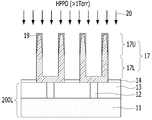
도 10e에 도시된 바와 같이, 제2플라즈마처리(34)에 의해 계면층(35)이 형성될 수 있다. 제2플라즈마처리(34)는 도 2c 및 도 5의 제2플라즈마처리(133, 133P)에 대응될 수 있다. 제2플라즈마처리(34)는 제1플라즈마처리(32)보다 높은 압력에서 수행될 수 있다. 예를 들어, 제2플라즈마처리(34)는 1torr보다 높은 압력에서 수행될 수 있다. 제2플라즈마처리(34)는 산소 분위기에서 수행될 수 있다. 제2플라즈마처리(34)는 고압플라즈마산화(HPPO)를 포함할 수 있다.The
상부 하부전극(31U)에서는 질소 환원 반응 및 산소 치환 반응에 의해 제1계면층(35U)이 형성될 수 있다. 하부 하부전극(31L)에서는 산화 반응에 의해 제2계면층(35L)이 형성될 수 있다. 제1계면층(35U)과 제2계면층(35L)은 동일한 두께일 수 있다. 제1계면층(35U)과 제2계면층(35L)은 연속된 층일 수 있다. 제1계면층(35U)과 제2계면층(35L)은 하부전극(31)의 상부면 및 외벽 상에 형성될 수 있다.In the upper
위와 같은 일련의 저압의 제1플라즈마처리(32) 및 고압의 제2플라즈마처리(34)를 순차적으로 수행하므로써, 하부전극(31)의 표면에 균일한 두께의 계면층(35)이 형성될 수 있다. 계면층(35)은 하부전극(31)의 표면을 산화시킨 산화물을 포함할 수 있다. 하부전극(31)이 금속의 질화물을 포함하는 경우, 계면층(35)은 금속의 산화물일 수 있다. 하부전극(31)이 티타늄질화물을 포함하는 경우, 계면층(35)은 티타늄산화물(TiO2)을 포함할 수 있다. The
도 10f에 도시된 바와 같이, 유전층(36)이 형성될 수 있다. 유전층(36)은 계면층(35) 상에 형성될 수 있다. 유전층(36)은 계면층(35)과 식각정지층(14)을 커버링할 수 있다. 유전층(36)은 실리콘산화물보다 유전율이 높은 고유전율 물질을 포함할 수 있다. 유전층(36)은 ZAZ(ZrO2/Al2O3/ZrO2)를 포함할 수 있다. 다른 실시예에서, 유전층(36)은 HAH(HfO2/Al2O3/HfO2) 를 포함할 수도 있다. 계면층(35)이 티타늄산화물을 포함하고, 유전층(36)이 ZAZ를 포함하는 경우, 하부전극(31) 상에 TZAZ(TiO2/ZrO2/Al2O3/ZrO2)로 이루어진 유전층 스택이 형성될 수 있다.10F, a
유전층(36)을 형성한 후, 유전층(36) 상에 상부전극(37)이 형성될 수 있다. 상부전극(37)은 하부전극(31)과 동일 재질의 물질을 포함할 수 있다. 상부전극(37)은 금속-베이스 물질을 포함할 수 있다. 본 실시예에서는 상부전극(37)은 원자층증착법에 의해 형성된 티타늄질화물(ALD-TiN)을 포함할 수 있다. 다른 실시예에서, 상부전극(37)은 다층 구조일 수 있다. 상부전극(37)은 제1금속함유층, 실리콘저마늄층 및 제2금속함유층을 차례로 적층하여 형성할 수도 있다. 예를 들어, 제1금속함유층은, 티타늄질화물일 수 있고, 제2금속함유층은 텅스텐질화물과 텅스텐이 적층된 WN/W일 수 있다. 실리콘저마늄층은 보론이 도핑될 수 있다.After forming the
도 11a 내지 도 11g는 제3실시예에 따른 반도체장치를 제조하는 방법의 제3예를 도시한 도면이다. 이하, 설명의 편의를 위해, 도 8a 내지 도 8c에 도시된 반도체장치(200)의 구성요소들 중에서 캐패시터(300) 하부에 위치하는 하부 구조물(200L)의 제조 방법은 공지된 방법을 참조하기로 한다. 11A to 11G are views showing a third example of a method of manufacturing the semiconductor device according to the third embodiment. Hereinafter, for convenience of explanation, a method of manufacturing the
도 11a에 도시된 바와 같이, 하부 구조물(200L)이 형성될 수 있다. 하부 구조물(200L)은 기판(11) 및 기판(11) 상에 형성된 스토리지노드콘택구조물(12)을 포함할 수 있다. 스토리지노드콘택구조물(12)은 층간절연층(13)을 관통하여 기판(11)과 접속될 수 있다. 스토리지노드콘택구조물(12)은 도 8a 내지 도 8c의 스토리지노드콘택구조물(SNC)에 대응할 수 있다. 도시하지 않았지만, 하부구조물(200L)은 셀트랜지스터, 비트라인콘택플러그, 비트라인을 더 포함할 수 있다. 하부 구조물(200L)의 상세 구성요소들은 도 8a 내지 도 8c를 참조하기로 한다.As shown in FIG. 11A, the
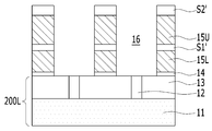
다음으로, 하부 구조물(200L) 상에 식각정지층(14)이 형성될 수 있다. 식각정지층(14) 상에 제1몰드층(15L), 제1서포터층(S1'), 제2몰드층(15U), 제2서포터층(S2')이 적층될 수 있다. 제1 및 제2몰드층(15L, 15U)은 절연물질을 포함할 수 있다. 제1 및 제2몰드층(15L, 15U)은 실리콘산화물을 포함할 수 있다. 제1몰드층(15L) 및 제2몰드층(15U)은 서로 다른 실리콘산화물로 형성될 수 있다. 제1서포터층(S1') 및 제2서포터층(S2')은 제1 및 제2몰드층(15L, 15U)에 대한 식각 선택성을 갖는 물질로 형성될 수 있다. 제1서포터층(S1') 및 제2서포터층(S2')은 실리콘 질화물, 실리콘탄소질화물(SiCN) 또는 이들의 조합을 포함할 수 있다.Next, an
식각정지층(14)은 제1 및 제2몰드층(15L, 15U)에 대한 식각 선택성을 갖는 물질로 형성될 수 있다. 식각정지층(14)은 실리콘 질화물을 포함할 수 있다.The
다음으로, 오프닝(16)이 형성될 수 있다. 오프닝(16)은 제2서포터층(S1'), 제2몰드층(15U), 제1서포터층(S1') 및 제1몰드층(15L)을 식각하여 형성될 수 있다. 오프닝(16)을 형성하기 위한 식각 공정은 식각정지층(14)에서 정지할 수 있다. 오프닝(16)은 하부전극(또는 스토리지노드)이 형성될 홀이라고 지칭될 수 있다. 오프닝(16)은 고종횡비를 가질 수 있다. 오프닝(16)은 적어도 1:1 이상의 종횡비를 가질 수 있다. 예를 들어, 오프닝(16)은 1:10 이상의 고종횡비를 가질 수 있다. Next, an
후속하여, 식각정지층(14)을 식각하여 오프닝(16) 아래의 스토리지노드콘택구조물(12)의 상부 표면을 노출시킬 수 있다.Subsequently, the
도 11b에 도시된 바와 같이, 오프닝(16) 내에 하부전극층(17A)이 형성될 수 있다. 하부전극층(17A)은 오프닝(16)의 프로파일 따라 컨포멀하게 형성될 수 있다.The
오프닝(16)에 하부전극층(17A)을 형성하기 위해서, 하부전극층(17A)은 단차 도포성이 우수한 막-형성 기술을 이용하여 형성될 수 있다. 예를 들어, 하부전극층(17A)은 화학기상증착법(CVD) 또는 원자층증착법(ALD)을 이용하여 형성될 수 있다. 하부전극층(17A)은 금속, 금속질화물 또는 이들의 조합을 포함할 수 있다. 하부전극층(17A)은 티타늄(Ti), 티타늄 질화물(TiN), 탄탈륨(Ta), 탄탈륨 질화물(TaN), 티타늄 알루미늄 질화물(TiAlN), 텅스텐(W) 또는 텅스텐 질화물(WN), 루테늄(Ru), 루테늄 산화물(RuO2), 이리듐(Ir), 이리듐 산화물(IrO2), 플래티늄(Pt) 또는 이들의 조합 중 적어도 하나를 포함할 수 있다. 본 실시예에서, 하부전극층(17A)은 티타늄 질화물(TiN)을 포함할 수 있다. 하부전극층(17A)은 원자층증착(ALD)에 의해 형성된 티타늄질화물(ALD-TiN)을 포함할 수 있다. 하부전극층(17A)은 화학양론적 조성비를 갖는 티타늄질화물일 수 있다. 화학양론적 조성비란 질소와 티타늄의 조성비가 1:1일 수 있다.In order to form the
도 11c에 도시된 바와 같이, 하부전극(17)이 형성될 수 있다. 하부전극(17)은 오프닝(16)의 내부에 위치할 수 있다. 하부전극(17)을 형성하기 위해, 하부전극층(17A)에 대해 선택적 제거 공정을 수행할 수 있다. 선택적 제거 공정은 화학적 기계 연마(CMP)공정 또는 에치백(Etch back) 공정일 수 있다. 예를 들어, 하부전극층(17A) 상에 오프닝(16)을 채우는 보호층(도시 생략)을 형성한 후, 제2서포터층(S2)의 표면이 노출될때까지 화학적기계적연마(CMP) 공정을 진행할 수 있다. As shown in FIG. 11C, the
하부전극(17)은 오프닝(16)의 바닥 및 측벽을 따라 위치하는 실린더 형상(Cylinder shape)일 수 있다. 하부전극(17)은 스토리지노드콘택구조물(12)에 전기적으로 연결될 수 있다.The
도 11d에 도시된 바와 같이, 제2서포터(S2) 및 제1서포터(S1)가 형성될 수 있다. 제2서포터층(S2') 및 제1서포터층(S1')을 선택적으로 식각하여 각각 제2서포터(S2) 및 제1서포터(S1)를 형성할 수 있다. 예를 들어, 제2서포터층(S2')의 식각에 의해 지지대 오프닝(SO) 및 제2서포터(S2)가 형성되고, 지지대 오프닝(SO)을 통해 제2몰드층(15U)을 제거한다. 계속해서, 제1서포터층(S1')을 식각하여 제1서포터(S1)를 한 후에 제1몰드층(15L)을 제거할 수 있다. 제2몰드층(15U)과 제1몰드층(15L)은 습식 딥아웃 공정에 의해 제거될 수 있다. 제2서포터(S2)는 하부전극(17)의 일측벽에 형성되어, 인접하는 다른 하부전극(17)의 일측벽과 접촉할 수 있다. 따라서, 제2서포터(S2)는 인접하는 복수 개의 하부전극(17)의 상부를 지지할 수 있다. 제1서포터(S1)는 하부전극(17)의 일측벽에 형성되어, 인접하는 하부전극(17)의 일측벽과 접촉할 수 있다. 따라서, 제1서포터(S1)는 인접하는 복수 개의 하부전극(17)의 하부를 지지할 수 있다. 제1몰드층(15L) 및 제2몰드층(15U)이 제거되어 식각정지층(14)이 노출될 수 있다. As shown in Fig. 11D, the second supporter S2 and the first supporter S1 may be formed. The second supporter layer S2 'and the first supporter layer S1' may be selectively etched to form the second supporter S2 and the first supporter S1. For example, the support opening SO and the second supporter S2 are formed by etching the second supporter layer S2 ', and the
제1 및 제2몰드층(15U, 15L)이 제거됨에 따라, 하부전극(17)의 내벽 및 외벽이 모두 노출될 수 있다. 하부전극(17)의 바닥 주위는 식각정지층(14)에 의해 지지될 수 있다.As the first and second mold layers 15U and 15L are removed, both the inner wall and the outer wall of the
하부전극(17)은 고종횡비를 가질 수 있다. 하부전극(17)은 오프닝(16)과 동일한 종횡비를 가질 수 있다. 예를 들어, 하부전극(17)은 1:10 이상의 고종횡비를 가질 수 있다.The
위와 같은 제1서포터(S1) 및 제2서포터(S2)는 하부전극(17)의 구조적 안정성을 증가시킬 수 있다.The first supporter S1 and the second supporter S2 may increase the structural stability of the
도 11e에 도시된 바와 같이, 제1플라즈마처리(41)에 의해 질소리치층(42)이 형성될 수 있다. 제1플라즈마처리(41)는 도 2a의 제1플라즈마처리(131)에 대응될 수 있다. 제1플라즈마처리(41)는 저압에서 수행될 수 있다. 제1플라즈마처리(41)가 저압에서 수행됨에 따라, 많은 양의 이온플라즈마를 형성시킬 수 있다. 이때, 이온플라즈마 효율을 높이기 위하여, 첨가가스를 추가할 수 있다. 첨가가스는 Ar 또는 He을 포함할 수 있다. As shown in Fig. 11E, the nitrogen-
제1플라즈마처리(41)는 저압 플라즈마질화(LPPN)를 포함할 수 있다. 제1플라즈마처리(41)는 저압에서 질소함유가스분위기로 수행될 수 있다. 예를 들어, 100mTorr 이하의 압력에서 N2 또는 NH3 가스를 사용할 수 있다. The
본 실시예에서, 제1플라즈마처리(41)가 질소분위기의 저압에서 수행되는 경우, 높은 반응력을 갖는 질소 이온플라즈마들은 하부전극(17)의 상부에 포격될 수 있다. 이러한 제1플라즈마처리(41)의 결과로써, 질소리치층(42)이 형성될 수 있다. 예를 들어, 하부전극(17)이 티타늄질화물인 경우, 질소리치층(42)은 질소리치 티타늄질화물(N rich TixNy)을 포함할 수 있다. 하부전극(17)은 하부 하부전극(17L)과 상부 하부전극(17U)을 포함할 수 있다. 상부 하부전극(17U)이 완전히 질소리치층(42)으로 변환되지 않을 수 있다. 상부 하부전극(17U)의 표면에 질소리치층(42)이 형성될 수 있다. 하부 하부전극(17L)은 비-플라즈마처리될 수 있다. 즉, 하부 하부전극(17L)은 질소리치층(42)을 포함하지 않을 수 있다.In this embodiment, when the
위와 같이, 제1플라즈마처리(41)에 의해 상부 하부전극(17U)에 국부적으로 질소리치층(42)을 형성할 수 있다. 질소리치층(42)에 의해 하부전극(17)은 불균일한 질소 프로파일을 갖게 된다. 하부 하부전극(17L)은 티타늄질화물로 잔류할 수 있고, 상부 하부전극(17U)은 티타늄질화물과 질소리치 티타늄질화물이 혼재될 수 있다. 따라서, 하부 하부전극(17L)과 상부 하부전극(17U)은 서로 다른 질소함량을 갖는 티타늄질화물이 될 수 있다. 부연하면, 상부 하부전극(17U)은 질소 리치 티타늄질화물로 형성되고, 하부 하부전극(17L)은 화학양론적조성을 갖는 티타늄질화물로 형성될 수 있다.As described above, the nitrogen-
본 실시예에서, 질소리치층(42)은 상부 하부전극(17U) 중에서 제2서포터(S2)와 접촉하지 않는 부분에 형성될 수 있다. 다른 실시예에서, 질소리치층(42)은 제2서포터(S2)와 접촉하는 부분 및 제2서포터(S2)와 접촉하지 않는 부분에 형성될 수도 있다.In this embodiment, the nitrogen-
도시하지 않았으나, 제2서포터(S2)가 제1플라즈마처리(41)에 노출되어 질화될 수 있다.Although not shown, the second supporter S2 may be exposed to the
도 11f에 도시된 바와 같이, 제2플라즈마처리(43)에 의해 계면층(44)이 형성될 수 있다. 제2플라즈마처리(43)는 도 2c의 제2플라즈마처리(133)에 대응될 수 있다. 제2플라즈마처리(43)는 제1플라즈마처리(41)보다 높은 압력에서 수행될 수 있다. 예를 들어, 제2플라즈마처리(43)는 1torr보다 높은 압력에서 수행될 수 있다. 제2플라즈마처리(43)는 산소 분위기에서 수행될 수 있다. 제2플라즈마처리(43)는 플라즈마산화를 포함할 수 있다.The
하부전극(17)의 상부에서는 질소 환원 반응 및 산소 치환 반응에 의해 제1계면층(44U)이 형성될 수 있다. 예컨대, 제1계면층(44U)은 질소리치층(42)의 영향을 받는다. 하부전극(17)의 하부에서는 산화 반응에 의해 제2계면층(44L)이 형성된다. 제1계면층(44U)과 제2계면층(44L)은 동일한 두께일 수 있다.At the upper portion of the
위와 같은 일련의 저압의 제1플라즈마처리(41) 및 고압의 제2플라즈마처리(43)를 순차적으로 수행하므로써, 하부전극(17)의 표면에 균일한 두께의 계면층(44)이 형성될 수 있다. 계면층(44)은 하부전극(17)의 표면을 산화시킨 산화물을 포함할 수 있다. 하부전극(17)이 금속의 질화물을 포함하는 경우, 계면층(44)은 금속의 산화물일 수 있다. 하부전극(17)이 티타늄질화물을 포함하는 경우, 계면층(44)은 티타늄산화물(TiO2)을 포함할 수 있다. The
본 실시예에서, 제1계면층(44U)은 상부 하부전극(17U) 중에서 제2서포터(S2)와 접촉하지 않는 부분에 형성될 수 있다. 즉, 하부전극(17)과 제2서포터(S2)의 계면에서는 제1계면층(44U)이 형성되지 않을 수 있다.In this embodiment, the
제2계면층(44L)은 하부 하부전극(17L) 중에서 제1서포터(S1)와 접촉하지 않는 부분에 형성될 수 있다. 즉, 하부전극(17)과 제1서포터(S1)의 계면에서는 제2계면층(44L)이 형성되지 않을 수 있다.The
도시하지 않았으나, 제1서포터(S1) 및 제2서포터(S2)의 표면들도 제2플라즈마처리(43)에 의해 산화될 수도 있다.Although not shown, the surfaces of the first supporter S1 and the second supporter S2 may be oxidized by the
도 11g에 도시된 바와 같이, 유전층(22)이 형성될 수 있다. 유전층(22)은 계면층(44) 상에 형성될 수 있다. 유전층(22)은 식각정지층(14), 제1 및 제2서포터(S1, S2)를 커버링할 수 있다.As shown in Fig. 11G, a
유전층(22)을 형성한 후, 유전층(22) 상에 상부전극(23)을 형성할 수 있다.After forming the
도 12a 내지 도 12g는 제3실시예에 따른 반도체장치를 제조하는 방법의 제4예를 도시한 도면이다. 이하, 설명의 편의를 위해, 도 8a 내지 도 8c에 도시된 반도체장치(200)의 구성요소들 중에서 캐패시터(300) 하부에 위치하는 하부 구조물(200L)의 제조 방법은 공지된 방법을 참조하기로 한다. 12A to 12G are views showing a fourth example of a method of manufacturing the semiconductor device according to the third embodiment. Hereinafter, for convenience of explanation, a method of manufacturing the
도 12a에 도시된 바와 같이, 하부 구조물(200L) 상에 식각정지층(14)이 형성될 수 있다. 식각정지층(14) 상에 제1몰드층(15L), 제1서포터층(S1'), 제2몰드층(15U), 제2서포터층(S2')이 적층될 수 있다. 제1 및 제2몰드층(15L, 15U)은 절연물질을 포함할 수 있다. 제1 및 제2몰드층(15L, 15U)은 실리콘산화물을 포함할 수 있다. 제1몰드층(15L) 및 제2몰드층(15U)은 서로 다른 실리콘산화물로 형성될 수 있다. 제1서포터층(S1') 및 제2서포터층(S2')은 제1 및 제2몰드층(15L, 15U)에 대한 식각 선택성을 갖는 물질로 형성될 수 있다. 제1서포터층(S1') 및 제2서포터층(S2')은 실리콘 질화물, 실리콘탄소질화물(SiCN) 또는 이들의 조합을 포함할 수 있다.As shown in FIG. 12A, the
식각정지층(14)은 제1 및 제2몰드층(15L, 15U)에 대한 식각 선택성을 갖는 물질로 형성될 수 있다. 식각정지층(14)은 실리콘 질화물을 포함할 수 있다.The
다음으로, 오프닝(16)이 형성될 수 있다. 오프닝(16)은 제2서포터층(S1'), 제2몰드층(15U), 제1서포터층(S1') 및 제1몰드층(15L)을 식각하여 형성될 수 있다. 오프닝(16)을 형성하기 위한 식각 공정은 식각정지층(14)에서 정지할 수 있다. 오프닝(16)은 하부전극(또는 스토리지노드)이 형성될 홀이라고 지칭될 수 있다. 오프닝(16)은 고종횡비를 가질 수 있다. 오프닝(16)은 적어도 1:1 이상의 종횡비를 가질 수 있다. 예를 들어, 오프닝(16)은 1:10 이상의 고종횡비를 가질 수 있다. Next, an
후속하여, 식각정지층(14)을 식각하여 오프닝(16) 아래의 스토리지노드콘택구조물(12)의 상부 표면을 노출시킬 수 있다.Subsequently, the
도 12b에 도시된 바와 같이, 오프닝(16) 내에 하부전극층(31A)이 형성될 수 있다. 하부전극층(31A)은 오프닝(16)의 내부를 채울 수 있다. 하부전극층(31A)은 오프닝(16)의 내부를 채우고, 몰드층(15) 상에 형성될 수 있다. 하부전극층(31A)은 금속, 금속질화물 또는 이들의 조합을 포함할 수 있다. 하부전극층(31A)은 티타늄(Ti), 티타늄 질화물(TiN), 탄탈륨(Ta), 탄탈륨 질화물(TaN), 티타늄 알루미늄 질화물(TiAlN), 텅스텐(W) 또는 텅스텐 질화물(WN), 루테늄(Ru), 루테늄 산화물(RuO2), 이리듐(Ir), 이리듐 산화물(IrO2), 플래티늄(Pt) 및 이들의 조합 중 적어도 하나를 포함할 수 있다. 본 실시예에서, 하부전극층(31A)은 티타늄 질화물(TiN)을 포함할 수 있다. 본 실시예에서, 하부전극층(31A)은 원자층증착법(ALD)에 의해 형성된 티타늄질화물(ALD-TiN)을 포함할 수 있다. 하부전극층(31A)은 화학양론적 조성비를 갖는 티타늄질화물일 수 있다. 화학양론적 조성비란 질소와 티타늄의 조성비가 1:1일 수 있다.The
도 12c에 도시된 바와 같이, 하부전극(31)이 형성될 수 있다. 하부전극(31)은 오프닝(16)의 내부에 위치할 수 있다. 하부전극(31)을 형성하기 위해, 하부전극층(31A)에 대해 선택적 제거 공정을 수행할 수 있다. 선택적 제거 공정은 화학적 기계 연마(CMP)공정 또는 에치백(Etch back) 공정일 수 있다. 예를 들어, 하부전극층(31A)에 대해 몰드층(15)의 표면이 노출될때까지 화학적기계적연마(CMP) 공정을 진행할 수 있다. 12C, the
하부전극(31)은 오프닝(16)의 내부를 채우는 필라 형상(Pillar shape)일 수 있다. 하부전극(31)은 스토리지노드콘택구조물(12)에 전기적으로 연결될 수 있다.The
도 12d에 도시된 바와 같이, 제2서포터(S2) 및 제1서포터(S1)가 형성될 수 있다. 제2서포터층(S2') 및 제1서포터층(S1')을 선택적으로 식각하여 각각 제2서포터(S2) 및 제1서포터(S1)를 형성할 수 있다. 예를 들어, 제2서포터층(S2')의 식각에 의해 지지대 오프닝(SO) 및 제2서포터(S2)가 형성되고, 지지대 오프닝(SO)을 통해 제2몰드층(15U)을 제거한다. 계속해서, 제1서포터층(S1')을 식각하여 제1서포터(S1)를 한 후에 제1몰드층(15L)을 제거할 수 있다. 제2몰드층(15U)과 제1몰드층(15L)은 습식 딥아웃 공정에 의해 제거될 수 있다. 제2서포터(S2)는 하부전극(31)의 일측벽에 형성되어, 인접하는 다른 하부전극(31)의 일측벽과 접촉할 수 있다. 따라서, 제2서포터(S2)는 인접하는 복수 개의 하부전극(31)의 상부영역을 지지할 수 있다. 제1서포터(S1)는 하부전극(31)의 일측벽에 형성되어, 인접하는 하부전극(31)의 일측벽과 접촉할 수 있다. 따라서, 제1서포터(S1)는 인접하는 복수 개의 하부전극(31)의 하부 영역을 지지할 수 있다. 제1몰드층(15L) 및 제2몰드층(15U)이 제거되어 식각정지층(14)이 노출될 수 있다. As shown in Fig. 12D, the second supporter S2 and the first supporter S1 may be formed. The second supporter layer S2 'and the first supporter layer S1' may be selectively etched to form the second supporter S2 and the first supporter S1. For example, the support opening SO and the second supporter S2 are formed by etching the second supporter layer S2 ', and the
제1 및 제2몰드층(15U, 15L)이 제거됨에 따라, 하부전극(31)의 외벽이 모두 노출될 수 있다. 하부전극(31)의 바닥 주위는 식각정지층(14)에 의해 지지될 수 있다.As the first and second mold layers 15U and 15L are removed, all the outer walls of the
하부전극(31)은 고종횡비를 가질 수 있다. 하부전극(31)은 오프닝(16)과 동일한 종횡비를 가질 수 있다. 예를 들어, 하부전극(31)은 1:10 이상의 고종횡비를 가질 수 있다.The
위와 같은 제1서포터(S1) 및 제2서포터(S2)는 하부전극(31)의 구조적 안정성을 증가시킬 수 있다.The first supporter S1 and the second supporter S2 may increase the structural stability of the
다른 실시예에서, 서포터층은 3층 이상의 다층 구조일 수도 있다.In another embodiment, the supporter layer may be a three-layer or more multi-layer structure.
도 12e에 도시된 바와 같이, 제1플라즈마처리(51)에 의해 질소리치층(52)이 형성될 수 있다. 제1플라즈마처리(51)는 도 2a 및 도 5의 제1플라즈마처리(131, 131P)에 대응될 수 있다. 제1플라즈마처리(51)는 저압에서 수행될 수 있다. 제1플라즈마처리(51)는 저압 플라즈마질화(LPPN)를 포함할 수 있다. 제1플라즈마처리(51)는 저압에서 질소함유가스분위기로 수행될 수 있다. 예를 들어, 100mTorr 이하의 압력에서 N2 또는 NH3 가스를 사용할 수 있다. As shown in FIG. 12E, the nitrogen-
본 실시예에서, 제1플라즈마처리(51)가 질소분위기의 저압에서 수행되는 경우, 높은 반응력을 갖는 질소 이온플라즈마들은 하부전극(31)의 상부에 포격될 수 있다. 이러한 제1플라즈마처리(51)의 결과로써, 질소리치층(52)이 형성될 수 있다. 예를 들어, 하부전극(31)이 티타늄질화물인 경우, 질소리치층(52)은 질소리치 티타늄질화물(N rich TixNy)을 포함할 수 있다. 하부전극(31)은 하부 하부전극(31L)과 상부 하부전극(31U)을 포함할 수 있다. 상부 하부전극(31U)이 완전히 질소리치층(52)으로 변환되지 않을 수 있다. 상부 하부전극(31U)의 표면에 질소리치층(52)이 형성될 수 있다. 하부 하부전극(31L)은 비-플라즈마처리될 수 있다. 즉, 하부 하부전극(31L)은 질소리치층(52)을 포함하지 않을 수 있다.In this embodiment, when the
위와 같이, 제1플라즈마처리(51)에 의해 상부 하부전극(31U)에 국부적으로 질소리치층(52)을 형성할 수 있다. 질소리치층(52)에 의해 하부전극(31)은 불균일한 질소 프로파일을 갖게 된다. 하부 하부전극(31L)은 티타늄질화물로 잔류할 수 있고, 상부 하부전극(31U)은 티타늄질화물과 질소리치 티타늄질화물이 혼재될 수 있다. 따라서, 하부 하부전극(31L)과 상부 하부전극(31U)은 서로 다른 질소함량을 갖는 티타늄질화물이 될 수 있다. 부연하면, 상부 하부전극(31U)은 질소 리치 티타늄질화물로 형성되고, 하부 하부전극(31L)은 화학양론적조성을 갖는 티타늄질화물로 형성될 수 있다.As described above, the nitrogen-
도 12f에 도시된 바와 같이, 제2플라즈마처리(53)에 의해 계면층(54)이 형성될 수 있다. 제2플라즈마처리(53)는 도 2c 및 도 5의 제1플라즈마처리(133, 133P)에 대응될 수 있다. 제2플라즈마처리(53)는 제1플라즈마처리(51)보다 높은 압력에서 수행될 수 있다. 예를 들어, 제2플라즈마처리(53)는 1torr보다 높은 압력에서 수행될 수 있다. 제2플라즈마처리(53)는 산소 분위기에서 수행될 수 있다. 제2플라즈마처리(53)는 플라즈마산화를 포함할 수 있다.As shown in FIG. 12F, the
상부 하부전극(31U)에서는 질소 환원 반응 및 산소 치환 반응에 의해 제1계면층(54U)이 형성되고, 하부 하부전극(31L)에서는 산화 반응에 의해 제2계면층(54L)이 형성된다. 제1계면층(54U)과 제2계면층(54L)은 동일한 두께일 수 있다. The
위와 같은 일련의 저압의 제1플라즈마처리(51) 및 고압의 제2플라즈마처리(53)를 순차적으로 수행하므로써, 하부전극(31)의 표면에 균일한 두께의 계면층(54)이 형성될 수 있다. 계면층(54)은 하부전극(31)의 표면을 산화시킨 산화물을 포함할 수 있다. 하부전극(31)이 금속의 질화물을 포함하는 경우, 계면층(54)은 금속의 산화물일 수 있다. 하부전극(31)이 티타늄질화물을 포함하는 경우, 계면층(54)은 티타늄산화물(TiO2)을 포함할 수 있다. The
본 실시예에서, 제1계면층(54U)은 상부 하부전극(31U) 중에서 제2서포터(S2)와 접촉하지 않는 부분에 형성될 수 있다. 즉, 하부전극(31)과 제2서포터(S2)의 계면에서는 제1계면층(54U)이 형성되지 않을 수 있다.In this embodiment, the
제2계면층(54L)은 하부 하부전극(31L) 중에서 제1서포터(S1)와 접촉하지 않는 부분에 형성될 수 있다. 즉, 하부전극(31)과 제1서포터(S1)의 계면에서는 제2계면층(54L)이 형성되지 않을 수 있다.The
도시하지 않았으나, 제1서포터(S1) 및 제2서포터(S2)의 표면들도 제2플라즈마처리(53)에 의해 산화될 수도 있다.Although not shown, the surfaces of the first supporter S1 and the second supporter S2 may also be oxidized by the second plasma treatment.
도 12g에 도시된 바와 같이, 계면층(54) 상에 유전층(36)이 형성될 수 있다. 유전층(36)은 식각정지층(14), 제1 및 제2서포터(S1, S2)를 커버링할 수 있다.As shown in FIG. 12G, a
유전층(36)을 형성한 후, 유전층(36) 상에 상부전극(37)을 형성할 수 있다. After forming the
전술한 본 발명은 전술한 실시예 및 첨부된 도면에 의해 한정되는 것이 아니고, 본 발명의 기술적 사상을 벗어나지 않는 범위 내에서 여러 가지 치환, 변형 및 변경이 가능하다는 것이 본 발명이 속하는 기술분야에서 통상의 지식을 가진 자에게 있어 명백할 것이다.It will be apparent to those skilled in the art that various modifications and variations can be made in the present invention without departing from the spirit or scope of the invention as defined by the appended claims. Will be clear to those who have knowledge of.
111 : 하부전극
112 : 계면층
113 : 유전층
114 : 상부전극111: lower electrode
112: interface layer
113: Dielectric layer
114: upper electrode
Claims (20)
상기 하부전극의 표면에 대해 제1플라즈마처리 및 제2플라즈마처리를 순차적으로 진행하여 계면층을 형성하는 단계;
상기 계면층 상에 유전층을 형성하는 단계; 및
상기 유전층 상에 상부전극을 형성하는 단계
를 포함하는 반도체장치 제조 방법.
Forming a lower electrode having a high aspect ratio;
Forming an interface layer by sequentially performing a first plasma process and a second plasma process on the surface of the lower electrode;
Forming a dielectric layer on the interfacial layer; And
Forming an upper electrode on the dielectric layer
≪ / RTI >
상기 계면층을 형성하는 단계에서,
상기 제1플라즈마처리는 이온플라즈마가 지배적인 분위기의 저압에서 수행하고,
상기 제2플라즈마처리는 라디칼플라즈마가 지배적인 분위기의 고압에서 수행하는
반도체장치 제조 방법.
The method according to claim 1,
In the step of forming the interface layer,
Wherein the first plasma treatment is performed at a low pressure in an atmosphere in which the ion plasma is dominant,
Wherein the second plasma treatment is performed at a high pressure in an atmosphere in which the radical plasma is dominant
A method of manufacturing a semiconductor device.
상기 제2플라즈마처리는 상기 제1플라즈마처리보다 높은 압력에서 수행되는 반도체장치 제조 방법.
The method according to claim 1,
Wherein the second plasma treatment is performed at a higher pressure than the first plasma treatment.
상기 제2플라즈마처리는 1Torr 보다 높은 압력에서 수행되고, 상기 제1플라즈마처리는 100mTorr보다 낮은 압력에서 수행되는 반도체장치 제조 방법.
The method according to claim 1,
Wherein the second plasma treatment is performed at a pressure higher than 1 Torr, and the first plasma treatment is performed at a pressure lower than 100 mTorr.
상기 계면층을 형성하는 단계에서,
상기 제1플라즈마처리는 질소이온플라즈마가 지배적인 분위기의 저압에서 수행하고,
상기 제2플라즈마처리는 산소라디칼플라즈마가 지배적인 분위기의 고압에서 수행하는
반도체장치 제조 방법.
The method according to claim 1,
In the step of forming the interface layer,
Wherein the first plasma treatment is performed at a low pressure in an atmosphere in which the nitrogen ion plasma is dominant,
Wherein the second plasma treatment is performed at a high pressure in an atmosphere in which the oxygen radical plasma is dominant
A method of manufacturing a semiconductor device.
상기 계면층을 형성하는 단계에서,
상기 제1플라즈마처리는 저압 플라즈마질화를 포함하고,
상기 제2플라즈마처리는 고압 플라즈마산화를 포함하는 반도체장치 제조 방법.
The method according to claim 1,
In the step of forming the interface layer,
Wherein the first plasma treatment comprises low pressure plasma nitridation,
Wherein the second plasma treatment comprises high pressure plasma oxidation.
상기 하부전극은, 적어도 1:10 이상의 종횡비를 갖는 실린더 형상을 포함하는 반도체장치 제조 방법.
The method according to claim 1,
Wherein the lower electrode comprises a cylinder shape having an aspect ratio of at least 1:10 or greater.
상기 하부전극은, 적어도 1:10 이상의 종횡비를 갖는 필라 형상을 포함하는 반도체장치 제조 방법.
The method according to claim 1,
Wherein the lower electrode comprises a pillar shape having an aspect ratio of at least 1:10 or greater.
상기 하부전극은 하부 하부전극과 상부 하부전극을 포함하고, 상기 제1플라즈마처리는 상기 상부 하부전극의 표면을 국부적으로 질화시키고, 상기 제2플라즈마처리는 상기 하부 하부전극 및 상기 질화된 상부 하부전극의 표면을 산화시키는 반도체장치 제조 방법.The method according to claim 1,
Wherein the lower electrode comprises a lower lower electrode and an upper lower electrode, the first plasma treatment locally nitriding the surface of the upper lower electrode, and the second plasma treatment is performed between the lower lower electrode and the nitrided upper lower electrode Wherein the surface of the semiconductor substrate is oxidized.
상기 하부전극은 금속질화물을 포함하는 반도체장치 제조 방법.
The method according to claim 1,
Wherein the lower electrode comprises a metal nitride.
상기 하부전극은 티타늄질화물 또는 탄탈륨질화물을 포함하는 반도체장치 제조 방법.
The method according to claim 1,
Wherein the lower electrode comprises titanium nitride or tantalum nitride.
상기 계면층은 금속산화물을 포함하는 반도체장치 제조 방법.
The method according to claim 1,
Wherein the interface layer comprises a metal oxide.
상기 계면층은 티타늄산화물 또는 탄탈륨산화물을 포함하는 반도체장치 제조 방법.
The method according to claim 1,
Wherein the interface layer comprises titanium oxide or tantalum oxide.
상기 유전층은 ZAZ(ZrO2/Al2O3/ZrO2) 또는 HAH(HfO2/Al2O3/HfO2)를 포함하는 반도체장치 제조 방법.
The method according to claim 1,
The dielectric layer is ZAZ (ZrO 2 / Al 2 O 3 / ZrO 2) or HAH (HfO 2 / Al 2 O 3 / HfO 2) method of manufacturing a semiconductor device comprising a.
상기 몰드층을 식각하여 오프닝을 형성하는 단계;
상기 오프닝 내에 금속질화물로 이루어진 하부전극을 형성하는 단계;
상기 몰드층을 제거하여 상기 하부전극을 노출시키는 단계;
상기 하부전극을 저압 플라즈마질화처리 및 고압 플라즈마산화처리에 순차적으로 노출시켜 상기 하부전극 상에 계면층을 형성하는 단계;
상기 계면층 상에 유전층을 형성하는 단계; 및
상기 유전층 상에 상부전극을 형성하는 단계
를 포함하는 반도체장치 제조 방법.
Forming a mold layer on the substructure;
Etching the mold layer to form an opening;
Forming a lower electrode made of a metal nitride in the opening;
Removing the mold layer to expose the lower electrode;
Sequentially exposing the lower electrode to a low-pressure plasma nitridation process and a high-pressure plasma oxidation process to form an interface layer on the lower electrode;
Forming a dielectric layer on the interfacial layer; And
Forming an upper electrode on the dielectric layer
≪ / RTI >
상기 저압 플라즈마질화처리는 질소이온플라즈마가 지배적인 분위기의 저압에서 수행하고,
상기 고압 플라즈마산화처리는 산소라디칼플라즈마가 지배적인 분위기의 고압에서 수행하는
반도체장치 제조 방법.
16. The method of claim 15,
Wherein the low pressure plasma nitridation process is performed at a low pressure in an atmosphere in which a nitrogen ion plasma is dominant,
The high pressure plasma oxidation treatment is performed at a high pressure in an atmosphere in which the oxygen radical plasma is dominant
A method of manufacturing a semiconductor device.
상기 고압 플라즈마산화처리는 1Torr 보다 높은 압력에서 수행되고, 상기 저압 플라즈마질화처리는 100mTorr보다 낮은 압력에서 수행되는 반도체장치 제조 방법.
16. The method of claim 15,
Wherein the high pressure plasma oxidation process is performed at a pressure higher than 1 Torr, and the low pressure plasma nitridation process is performed at a pressure lower than 100 mTorr.
상기 하부전극은, 적어도 1:10 이상의 종횡비를 갖는 실린더 형상 또는 필라 형상을 포함하는 반도체장치 제조 방법.
16. The method of claim 15,
Wherein the lower electrode comprises a cylinder shape or a pillar shape having an aspect ratio of at least 1:10 or more.
상기 하부전극은 티타늄질화물 또는 탄탈륨질화물을 포함하는 반도체장치 제조 방법.
16. The method of claim 15,
Wherein the lower electrode comprises titanium nitride or tantalum nitride.
상기 계면층은 티타늄산화물 또는 탄탈륨산화물을 포함하는 반도체장치 제조 방법.16. The method of claim 15,
Wherein the interface layer comprises titanium oxide or tantalum oxide.
Priority Applications (4)
| Application Number | Priority Date | Filing Date | Title |
|---|---|---|---|
| KR1020170033829A KR102372096B1 (en) | 2017-03-17 | 2017-03-17 | Semiconductor device and method for fabricating the same |
| US15/835,629 US10672772B2 (en) | 2017-03-17 | 2017-12-08 | Semiconductor device and method for fabricating the same |
| CN201810083257.6A CN108630686B (en) | 2017-03-17 | 2018-01-29 | Semiconductor device and manufacturing method thereof |
| US16/859,523 US10910383B2 (en) | 2017-03-17 | 2020-04-27 | Semiconductor device and method for fabricating the same |
Applications Claiming Priority (1)
| Application Number | Priority Date | Filing Date | Title |
|---|---|---|---|
| KR1020170033829A KR102372096B1 (en) | 2017-03-17 | 2017-03-17 | Semiconductor device and method for fabricating the same |
Publications (2)
| Publication Number | Publication Date |
|---|---|
| KR20180106149A true KR20180106149A (en) | 2018-10-01 |
| KR102372096B1 KR102372096B1 (en) | 2022-03-17 |
Family
ID=63520092
Family Applications (1)
| Application Number | Title | Priority Date | Filing Date |
|---|---|---|---|
| KR1020170033829A Active KR102372096B1 (en) | 2017-03-17 | 2017-03-17 | Semiconductor device and method for fabricating the same |
Country Status (3)
| Country | Link |
|---|---|
| US (2) | US10672772B2 (en) |
| KR (1) | KR102372096B1 (en) |
| CN (1) | CN108630686B (en) |
Cited By (4)
| Publication number | Priority date | Publication date | Assignee | Title |
|---|---|---|---|---|
| KR20200038662A (en) * | 2018-10-04 | 2020-04-14 | 삼성전자주식회사 | Methods for manufacturing semiconductor devices |
| KR20200101716A (en) * | 2019-02-20 | 2020-08-28 | 에스케이하이닉스 주식회사 | Semiconductor device and method for manufacturing the same |
| KR20210117794A (en) * | 2020-03-20 | 2021-09-29 | 에스케이하이닉스 주식회사 | Semiconductor device and method for fabricating the same |
| US12278261B2 (en) | 2021-07-23 | 2025-04-15 | Samsung Electronics Co., Ltd. | Capacitor, electronic device including the same, and method of manufacturing the same |
Families Citing this family (16)
| Publication number | Priority date | Publication date | Assignee | Title |
|---|---|---|---|---|
| KR102372096B1 (en) * | 2017-03-17 | 2022-03-17 | 에스케이하이닉스 주식회사 | Semiconductor device and method for fabricating the same |
| JP2018157114A (en) * | 2017-03-17 | 2018-10-04 | 東芝メモリ株式会社 | Storage device |
| CN109920760B (en) * | 2017-12-12 | 2021-01-12 | 联华电子股份有限公司 | Method for forming semiconductor device |
| TWI683418B (en) * | 2018-06-26 | 2020-01-21 | 華邦電子股份有限公司 | Dynamic random access memory and methods of manufacturing, reading and writing the same |
| KR102645594B1 (en) | 2019-03-29 | 2024-03-11 | 에스케이하이닉스 주식회사 | Semiconductor device and method for fabricating the same |
| KR102839363B1 (en) * | 2019-04-17 | 2025-07-29 | 에스케이하이닉스 주식회사 | Semiconductor device and method for manufacturing the same |
| US12082395B2 (en) * | 2019-06-14 | 2024-09-03 | Samsung Electronics Co., Ltd. | Semiconductor memory devices and methods of fabricating the same |
| US11152371B2 (en) * | 2019-08-13 | 2021-10-19 | Micron Technology, Inc. | Apparatus comprising monocrystalline semiconductor materials and monocrystalline metal silicide materials, and related methods, electronic devices, and electronic systems |
| KR102733324B1 (en) * | 2019-08-30 | 2024-11-25 | 에스케이하이닉스 주식회사 | Capacitor and method for manufacturing the same |
| KR102675933B1 (en) | 2019-11-01 | 2024-06-18 | 삼성전자주식회사 | Semiconductor memory device and method of fabricating the same |
| CN114068539A (en) * | 2020-07-31 | 2022-02-18 | 中国科学院微电子研究所 | Semiconductor capacitor structure, manufacturing method thereof, memory and electronic equipment |
| KR102782256B1 (en) | 2020-09-16 | 2025-03-18 | 삼성전자주식회사 | Semiconductor device and method of fabricating the same |
| US11417574B2 (en) * | 2020-10-29 | 2022-08-16 | Nanya Technology Corporation | Semiconductor device with testing structure and method for fabricating the same |
| US11812606B2 (en) * | 2021-03-05 | 2023-11-07 | Micron Technology, Inc. | Semiconductor device having gate trench |
| KR20230049469A (en) | 2021-10-06 | 2023-04-13 | 삼성전자주식회사 | Integrated circuit device |
| US11804404B2 (en) * | 2021-10-14 | 2023-10-31 | Nanya Technology Corporation | Method of forming a semicondcutor device using carbon containing spacer for a bitline |
Citations (6)
| Publication number | Priority date | Publication date | Assignee | Title |
|---|---|---|---|---|
| US6180481B1 (en) * | 1998-01-09 | 2001-01-30 | Micron Technology, Inc. | Barrier layer fabrication methods |
| US20030042528A1 (en) * | 2001-08-30 | 2003-03-06 | Leonard Forbes | Sram cells with repressed floating gate memory, low tunnel barrier interpoly insulators |
| US20070166921A1 (en) * | 2005-12-29 | 2007-07-19 | Hynix Semiconductor Inc. | Flash memory device and method of manufacturing the same |
| KR20080006270A (en) * | 2006-07-12 | 2008-01-16 | 삼성전자주식회사 | Manufacturing method of nonvolatile memory device |
| US20100062603A1 (en) * | 2008-09-11 | 2010-03-11 | Udayan Ganguly | Semiconductor devices suitable for narrow pitch applications and methods of fabrication thereof |
| KR20140136143A (en) * | 2013-05-20 | 2014-11-28 | 삼성전자주식회사 | Method of forming a capacitor and method of manufacturing a semiconductor device using the same |
Family Cites Families (5)
| Publication number | Priority date | Publication date | Assignee | Title |
|---|---|---|---|---|
| KR20120051820A (en) * | 2010-11-15 | 2012-05-23 | 삼성전자주식회사 | A capacitor, method for forming the same, semiconductor device including the same and method for manufacturing the same |
| US20120235276A1 (en) | 2011-03-18 | 2012-09-20 | Intermolecular, Inc. | Electrode treatments for enhanced dram performance |
| KR101934037B1 (en) * | 2012-11-21 | 2018-12-31 | 삼성전자주식회사 | Semiconductor device having supporter and method of forming the same |
| JP2014229680A (en) | 2013-05-21 | 2014-12-08 | ピーエスフォー ルクスコ エスエイアールエルPS4 Luxco S.a.r.l. | Semiconductor device and manufacturing method of the same |
| KR102372096B1 (en) * | 2017-03-17 | 2022-03-17 | 에스케이하이닉스 주식회사 | Semiconductor device and method for fabricating the same |
-
2017
- 2017-03-17 KR KR1020170033829A patent/KR102372096B1/en active Active
- 2017-12-08 US US15/835,629 patent/US10672772B2/en active Active
-
2018
- 2018-01-29 CN CN201810083257.6A patent/CN108630686B/en active Active
-
2020
- 2020-04-27 US US16/859,523 patent/US10910383B2/en active Active
Patent Citations (6)
| Publication number | Priority date | Publication date | Assignee | Title |
|---|---|---|---|---|
| US6180481B1 (en) * | 1998-01-09 | 2001-01-30 | Micron Technology, Inc. | Barrier layer fabrication methods |
| US20030042528A1 (en) * | 2001-08-30 | 2003-03-06 | Leonard Forbes | Sram cells with repressed floating gate memory, low tunnel barrier interpoly insulators |
| US20070166921A1 (en) * | 2005-12-29 | 2007-07-19 | Hynix Semiconductor Inc. | Flash memory device and method of manufacturing the same |
| KR20080006270A (en) * | 2006-07-12 | 2008-01-16 | 삼성전자주식회사 | Manufacturing method of nonvolatile memory device |
| US20100062603A1 (en) * | 2008-09-11 | 2010-03-11 | Udayan Ganguly | Semiconductor devices suitable for narrow pitch applications and methods of fabrication thereof |
| KR20140136143A (en) * | 2013-05-20 | 2014-11-28 | 삼성전자주식회사 | Method of forming a capacitor and method of manufacturing a semiconductor device using the same |
Cited By (6)
| Publication number | Priority date | Publication date | Assignee | Title |
|---|---|---|---|---|
| KR20200038662A (en) * | 2018-10-04 | 2020-04-14 | 삼성전자주식회사 | Methods for manufacturing semiconductor devices |
| US12074023B2 (en) | 2018-10-04 | 2024-08-27 | Samsung Electronics Co., Ltd. | Methods of manufacturing semiconductor devices |
| KR20200101716A (en) * | 2019-02-20 | 2020-08-28 | 에스케이하이닉스 주식회사 | Semiconductor device and method for manufacturing the same |
| KR20210117794A (en) * | 2020-03-20 | 2021-09-29 | 에스케이하이닉스 주식회사 | Semiconductor device and method for fabricating the same |
| US12082396B2 (en) | 2020-03-20 | 2024-09-03 | SK Hynix Inc. | Semiconductor device and method for fabricating the same |
| US12278261B2 (en) | 2021-07-23 | 2025-04-15 | Samsung Electronics Co., Ltd. | Capacitor, electronic device including the same, and method of manufacturing the same |
Also Published As
| Publication number | Publication date |
|---|---|
| US10672772B2 (en) | 2020-06-02 |
| US20180269211A1 (en) | 2018-09-20 |
| US10910383B2 (en) | 2021-02-02 |
| CN108630686A (en) | 2018-10-09 |
| CN108630686B (en) | 2022-12-13 |
| KR102372096B1 (en) | 2022-03-17 |
| US20200258888A1 (en) | 2020-08-13 |
Similar Documents
| Publication | Publication Date | Title |
|---|---|---|
| KR102372096B1 (en) | Semiconductor device and method for fabricating the same | |
| US12322745B2 (en) | Integrated circuit devices and methods of manufacturing the same | |
| CN112447905B (en) | Capacitor and method for manufacturing the same | |
| US7029985B2 (en) | Method of forming MIS capacitor | |
| US20210043632A1 (en) | Buried word line of a dynamic random access memory and method for fabricating the same | |
| JP3993972B2 (en) | Semiconductor device manufacturing method and semiconductor device | |
| CN115472743A (en) | Semiconductor device and method for manufacturing the same | |
| TWI849611B (en) | Semiconductor device | |
| CN114725070A (en) | Semiconductor device and method for manufacturing the same | |
| US12199140B2 (en) | Semiconductor device and method for manufacturing the same | |
| US20240244830A1 (en) | Semiconductor device | |
| TWI852569B (en) | Semiconductor device | |
| KR20250033757A (en) | Semiconductor device | |
| US11758713B2 (en) | Semiconductor devices | |
| JP7354088B2 (en) | Semiconductor device and its manufacturing method | |
| KR102633069B1 (en) | Semiconductor device and method for manufacturing the same | |
| KR100677769B1 (en) | Capacitor and manufacturing method thereof | |
| US20250188607A1 (en) | Method of manufacturing thin film | |
| KR102851930B1 (en) | Semiconductor device and method for fabricating the same | |
| KR100476379B1 (en) | Method for fabricating capacitor | |
| KR20250007364A (en) | Semiconductor memory device and manufacturing method of the same | |
| TW202431942A (en) | Semiconductor device | |
| JP2007306003A (en) | Semiconductor device manufacturing method and semiconductor device | |
| KR20230052567A (en) | Semiconductor device and method for fabricating the same | |
| KR20060019491A (en) | MEM capacitor manufacturing methods using metal nitride film as lower electrode |
Legal Events
| Date | Code | Title | Description |
|---|---|---|---|
| PA0109 | Patent application |
Patent event code: PA01091R01D Comment text: Patent Application Patent event date: 20170317 |
|
| PG1501 | Laying open of application | ||
| A201 | Request for examination | ||
| PA0201 | Request for examination |
Patent event code: PA02012R01D Patent event date: 20200302 Comment text: Request for Examination of Application Patent event code: PA02011R01I Patent event date: 20170317 Comment text: Patent Application |
|
| E902 | Notification of reason for refusal | ||
| PE0902 | Notice of grounds for rejection |
Comment text: Notification of reason for refusal Patent event date: 20210223 Patent event code: PE09021S01D |
|
| E90F | Notification of reason for final refusal | ||
| PE0902 | Notice of grounds for rejection |
Comment text: Final Notice of Reason for Refusal Patent event date: 20210825 Patent event code: PE09021S02D |
|
| E701 | Decision to grant or registration of patent right | ||
| PE0701 | Decision of registration |
Patent event code: PE07011S01D Comment text: Decision to Grant Registration Patent event date: 20220209 |
|
| PR0701 | Registration of establishment |
Comment text: Registration of Establishment Patent event date: 20220303 Patent event code: PR07011E01D |
|
| PR1002 | Payment of registration fee |
Payment date: 20220304 End annual number: 3 Start annual number: 1 |
|
| PG1601 | Publication of registration | ||
| PR1001 | Payment of annual fee |
Payment date: 20250225 Start annual number: 4 End annual number: 4 |