KR20180097779A - Methods and apparatus for calibrating for transconductance or gain over process or condition variations in differential circuits - Google Patents
Methods and apparatus for calibrating for transconductance or gain over process or condition variations in differential circuits Download PDFInfo
- Publication number
- KR20180097779A KR20180097779A KR1020187024085A KR20187024085A KR20180097779A KR 20180097779 A KR20180097779 A KR 20180097779A KR 1020187024085 A KR1020187024085 A KR 1020187024085A KR 20187024085 A KR20187024085 A KR 20187024085A KR 20180097779 A KR20180097779 A KR 20180097779A
- Authority
- KR
- South Korea
- Prior art keywords
- reference signal
- differential
- circuit
- current
- types
- Prior art date
- Legal status (The legal status is an assumption and is not a legal conclusion. Google has not performed a legal analysis and makes no representation as to the accuracy of the status listed.)
- Withdrawn
Links
- 238000000034 method Methods 0.000 title claims abstract description 75
- 230000008569 process Effects 0.000 title claims abstract description 34
- 239000000872 buffer Substances 0.000 claims description 44
- 238000010586 diagram Methods 0.000 description 8
- 101001005165 Bos taurus Lens fiber membrane intrinsic protein Proteins 0.000 description 6
- 230000008901 benefit Effects 0.000 description 4
- 238000012937 correction Methods 0.000 description 3
- 230000008878 coupling Effects 0.000 description 3
- 238000010168 coupling process Methods 0.000 description 3
- 238000005859 coupling reaction Methods 0.000 description 3
- 238000013461 design Methods 0.000 description 3
- 230000006870 function Effects 0.000 description 3
- 230000014509 gene expression Effects 0.000 description 3
- 239000007795 chemical reaction product Substances 0.000 description 2
- 238000004891 communication Methods 0.000 description 2
- 239000013067 intermediate product Substances 0.000 description 2
- 238000013459 approach Methods 0.000 description 1
- 239000003990 capacitor Substances 0.000 description 1
- 230000008859 change Effects 0.000 description 1
- 238000010276 construction Methods 0.000 description 1
- 239000012467 final product Substances 0.000 description 1
- 239000002184 metal Substances 0.000 description 1
- -1 mobile phone Substances 0.000 description 1
- 238000012986 modification Methods 0.000 description 1
- 230000004048 modification Effects 0.000 description 1
- 230000003287 optical effect Effects 0.000 description 1
- 239000000047 product Substances 0.000 description 1
- 230000011664 signaling Effects 0.000 description 1
Images


Classifications
-
- H—ELECTRICITY
- H03—ELECTRONIC CIRCUITRY
- H03F—AMPLIFIERS
- H03F1/00—Details of amplifiers with only discharge tubes, only semiconductor devices or only unspecified devices as amplifying elements
- H03F1/30—Modifications of amplifiers to reduce influence of variations of temperature or supply voltage or other physical parameters
-
- H—ELECTRICITY
- H03—ELECTRONIC CIRCUITRY
- H03F—AMPLIFIERS
- H03F3/00—Amplifiers with only discharge tubes or only semiconductor devices as amplifying elements
- H03F3/45—Differential amplifiers
- H03F3/45071—Differential amplifiers with semiconductor devices only
- H03F3/45076—Differential amplifiers with semiconductor devices only characterised by the way of implementation of the active amplifying circuit in the differential amplifier
- H03F3/45179—Differential amplifiers with semiconductor devices only characterised by the way of implementation of the active amplifying circuit in the differential amplifier using MOSFET transistors as the active amplifying circuit
- H03F3/45183—Long tailed pairs
-
- H—ELECTRICITY
- H03—ELECTRONIC CIRCUITRY
- H03F—AMPLIFIERS
- H03F3/00—Amplifiers with only discharge tubes or only semiconductor devices as amplifying elements
- H03F3/45—Differential amplifiers
- H03F3/45071—Differential amplifiers with semiconductor devices only
- H03F3/45076—Differential amplifiers with semiconductor devices only characterised by the way of implementation of the active amplifying circuit in the differential amplifier
- H03F3/45179—Differential amplifiers with semiconductor devices only characterised by the way of implementation of the active amplifying circuit in the differential amplifier using MOSFET transistors as the active amplifying circuit
- H03F3/45197—Pl types
-
- H—ELECTRICITY
- H03—ELECTRONIC CIRCUITRY
- H03F—AMPLIFIERS
- H03F3/00—Amplifiers with only discharge tubes or only semiconductor devices as amplifying elements
- H03F3/45—Differential amplifiers
- H03F3/45071—Differential amplifiers with semiconductor devices only
- H03F3/45479—Differential amplifiers with semiconductor devices only characterised by the way of common mode signal rejection
- H03F3/45632—Differential amplifiers with semiconductor devices only characterised by the way of common mode signal rejection in differential amplifiers with FET transistors as the active amplifying circuit
- H03F3/45636—Differential amplifiers with semiconductor devices only characterised by the way of common mode signal rejection in differential amplifiers with FET transistors as the active amplifying circuit by using feedback means
- H03F3/45641—Measuring at the loading circuit of the differential amplifier
- H03F3/4565—Controlling the common source circuit of the differential amplifier
-
- H—ELECTRICITY
- H03—ELECTRONIC CIRCUITRY
- H03F—AMPLIFIERS
- H03F3/00—Amplifiers with only discharge tubes or only semiconductor devices as amplifying elements
- H03F3/45—Differential amplifiers
- H03F3/45071—Differential amplifiers with semiconductor devices only
- H03F3/45479—Differential amplifiers with semiconductor devices only characterised by the way of common mode signal rejection
- H03F3/45632—Differential amplifiers with semiconductor devices only characterised by the way of common mode signal rejection in differential amplifiers with FET transistors as the active amplifying circuit
- H03F3/45744—Differential amplifiers with semiconductor devices only characterised by the way of common mode signal rejection in differential amplifiers with FET transistors as the active amplifying circuit by offset reduction
- H03F3/45766—Differential amplifiers with semiconductor devices only characterised by the way of common mode signal rejection in differential amplifiers with FET transistors as the active amplifying circuit by offset reduction by using balancing means
-
- H—ELECTRICITY
- H03—ELECTRONIC CIRCUITRY
- H03G—CONTROL OF AMPLIFICATION
- H03G1/00—Details of arrangements for controlling amplification
- H03G1/0005—Circuits characterised by the type of controlling devices operated by a controlling current or voltage signal
- H03G1/0017—Circuits characterised by the type of controlling devices operated by a controlling current or voltage signal the device being at least one of the amplifying solid-state elements
- H03G1/0029—Circuits characterised by the type of controlling devices operated by a controlling current or voltage signal the device being at least one of the amplifying solid-state elements using field-effect transistors [FET]
-
- H—ELECTRICITY
- H03—ELECTRONIC CIRCUITRY
- H03G—CONTROL OF AMPLIFICATION
- H03G3/00—Gain control in amplifiers or frequency changers
- H03G3/20—Automatic control
- H03G3/30—Automatic control in amplifiers having semiconductor devices
- H03G3/3036—Automatic control in amplifiers having semiconductor devices in high-frequency amplifiers or in frequency-changers
-
- H—ELECTRICITY
- H03—ELECTRONIC CIRCUITRY
- H03K—PULSE TECHNIQUE
- H03K19/00—Logic circuits, i.e. having at least two inputs acting on one output; Inverting circuits
- H03K19/003—Modifications for increasing the reliability for protection
- H03K19/00369—Modifications for compensating variations of temperature, supply voltage or other physical parameters
- H03K19/00384—Modifications for compensating variations of temperature, supply voltage or other physical parameters in field effect transistor circuits
-
- H—ELECTRICITY
- H03—ELECTRONIC CIRCUITRY
- H03K—PULSE TECHNIQUE
- H03K19/00—Logic circuits, i.e. having at least two inputs acting on one output; Inverting circuits
- H03K19/0175—Coupling arrangements; Interface arrangements
- H03K19/0185—Coupling arrangements; Interface arrangements using field effect transistors only
- H03K19/018507—Interface arrangements
- H03K19/018521—Interface arrangements of complementary type, e.g. CMOS
- H03K19/018528—Interface arrangements of complementary type, e.g. CMOS with at least one differential stage
-
- H—ELECTRICITY
- H03—ELECTRONIC CIRCUITRY
- H03F—AMPLIFIERS
- H03F2200/00—Indexing scheme relating to amplifiers
- H03F2200/447—Indexing scheme relating to amplifiers the amplifier being protected to temperature influence
-
- H—ELECTRICITY
- H03—ELECTRONIC CIRCUITRY
- H03F—AMPLIFIERS
- H03F2200/00—Indexing scheme relating to amplifiers
- H03F2200/543—A transmission line being used as coupling element between two amplifying stages
-
- H—ELECTRICITY
- H03—ELECTRONIC CIRCUITRY
- H03F—AMPLIFIERS
- H03F2203/00—Indexing scheme relating to amplifiers with only discharge tubes or only semiconductor devices as amplifying elements covered by H03F3/00
- H03F2203/45—Indexing scheme relating to differential amplifiers
- H03F2203/45048—Calibrating and standardising a dif amp
-
- H—ELECTRICITY
- H03—ELECTRONIC CIRCUITRY
- H03F—AMPLIFIERS
- H03F2203/00—Indexing scheme relating to amplifiers with only discharge tubes or only semiconductor devices as amplifying elements covered by H03F3/00
- H03F2203/45—Indexing scheme relating to differential amplifiers
- H03F2203/45101—Control of the DC level being present
-
- H—ELECTRICITY
- H03—ELECTRONIC CIRCUITRY
- H03F—AMPLIFIERS
- H03F2203/00—Indexing scheme relating to amplifiers with only discharge tubes or only semiconductor devices as amplifying elements covered by H03F3/00
- H03F2203/45—Indexing scheme relating to differential amplifiers
- H03F2203/45116—Feedback coupled to the input of the differential amplifier
-
- H—ELECTRICITY
- H03—ELECTRONIC CIRCUITRY
- H03F—AMPLIFIERS
- H03F2203/00—Indexing scheme relating to amplifiers with only discharge tubes or only semiconductor devices as amplifying elements covered by H03F3/00
- H03F2203/45—Indexing scheme relating to differential amplifiers
- H03F2203/45244—Indexing scheme relating to differential amplifiers the differential amplifier contains one or more explicit bias circuits, e.g. to bias the tail current sources, to bias the load transistors
-
- H—ELECTRICITY
- H03—ELECTRONIC CIRCUITRY
- H03F—AMPLIFIERS
- H03F2203/00—Indexing scheme relating to amplifiers with only discharge tubes or only semiconductor devices as amplifying elements covered by H03F3/00
- H03F2203/45—Indexing scheme relating to differential amplifiers
- H03F2203/45456—Indexing scheme relating to differential amplifiers the CSC comprising bias stabilisation means, e.g. DC-level stability, positive or negative temperature coefficient dependent control
Landscapes
- Engineering & Computer Science (AREA)
- Power Engineering (AREA)
- Computer Hardware Design (AREA)
- Physics & Mathematics (AREA)
- Computing Systems (AREA)
- General Engineering & Computer Science (AREA)
- Mathematical Physics (AREA)
- Amplifiers (AREA)
- Logic Circuits (AREA)
Abstract
장치가 제공된다. 장치는, 기준 신호(VREF)를 생성하도록 구성되는 교정 회로(200), 및 적어도 하나의 차동 회로를 포함하며, 적어도 하나의 차동 회로 각각은, 기준 신호에 기초하여, 프로세스 또는 조건 변동들에 따라, 교정된 트랜스컨덕턴스에서 동작하도록 구성된다. 교정 회로(200)는, 적어도 하나의 차동 회로와는 독립적으로 기준 신호(VREF)를 생성하도록 구성될 수 있다. 적어도 하나의 차동 회로를 동작시키기 위한 방법이 제공된다. 방법은, 기준 신호(VREF)를 생성하는 단계, 및 기준 신호에 기초하여, 프로세스 또는 조건 변동들에 따라, 교정된 트랜스컨덕턴스 또는 이득에서 적어도 하나의 차동 회로를 동작시키는 단계를 포함한다. 기준 신호(VREF)는 적어도 하나의 차동 회로와는 독립적으로 생성될 수 있다.Device is provided. The apparatus includes a calibration circuit (200) configured to generate a reference signal (VREF), and at least one differential circuit, wherein each of the at least one differential circuit , And is configured to operate at a calibrated transconductance. The calibration circuit 200 may be configured to generate the reference signal VREF independently of the at least one differential circuit. A method for operating at least one differential circuit is provided. The method includes generating a reference signal (VREF) and operating at least one differential circuit at a calibrated transconductance or gain, in accordance with process or condition variations, based on the reference signal. The reference signal VREF may be generated independently of at least one differential circuit.

Description
관련 출원에 대한 상호-참조Cross-reference to related application
[0001] 본 출원은 "METHODS AND APPARATUS FOR CALIBRATING FOR TRANSCONDUCTANCE OR GAIN OVER PROCESS OR CONDITION VARIATIONS IN DIFFERENTIAL CIRCUITS"이라는 명칭으로 2015년 1월 12일자로 출원된 미국 특허 출원 제 14/595,106호를 우선권으로 주장하며, 상기 미국 특허 출원은 그 전체가 인용에 의해 본원에 명백히 포함된다.[0001] This application claims priority to United States Patent Application Serial No. 14 / 595,106, filed January 12, 2015, entitled " METHODS AND APPARATUS FOR CALIBRATING FOR TRANSCONDUCTOR OR GAIN OVER PROCESS OR CONDITION VARIATIONS IN DIFFERENTIAL CIRCUITS, A patent application is expressly incorporated herein by reference in its entirety.
[0002] 본 개시내용은 일반적으로 전자 회로들에 관한 것으로, 더 상세하게는, 차동 회로들의 트랜스컨덕턴스(transconductance) 또는 이득을 교정(calibrate)하기 위한 장치들 및 방법들에 관한 것이다.[0002] The present disclosure relates generally to electronic circuits and, more particularly, to devices and methods for calibrating the transconductance or gain of differential circuits.
[0003] 차동 로직 계열들은 무선 통신을 위한 장치들 및 프로세서들에서 인기를 얻고 있다. 태블릿 컴퓨터들 및 셀 폰들과 같은 무선 장치들은 특정 이점들로 인해 차동 로직 회로들을 활용하는 프로세서들을 채택할 수 있다. 차동 로직 계열들의 예들은 CML(common-mode logic) 및 LVDS(low-voltage differential signaling) 회로들(예컨대, 게이트들)을 포함할 수 있다.[0003] Differential logic families are gaining popularity in devices and processors for wireless communications. Wireless devices such as tablet computers and cell phones may employ processors that utilize differential logic circuits due to certain advantages. Examples of differential logic families may include common-mode logic (CML) and low-voltage differential signaling (LVDS) circuits (e.g., gates).
[0004] 이들 차동 회로들은, 예를 들어, 제한된 전압 스윙(swing)들을 갖는 고속 데이터 통신의 이점들을 제공한다. 이들 차동 회로들은, SerDes(Serializer/Deserializer) 인터페이스들과 같은 애플리케이션들에 대해 적합할 수 있다. [0004] These differential circuits provide, for example, the advantages of high speed data communication with limited voltage swings. These differential circuits may be suitable for applications such as SerDes (Serializer / Deserializer) interfaces.
[0005] 차동 회로들을 채택하기 위한 하나의 설계 과제는, 프로세스 또는 조건 변동들(이를테면, 전압 및/또는 온도에서의 변동들; 총체적으로 PVT 변동들)에 따라 이들 회로들을 동작시키는 것이다.[0005] One design challenge for employing differential circuits is to operate these circuits in accordance with process or condition variations (such as variations in voltage and / or temperature, generally PVT variations).
[0006] 장치의 양상들이 제공된다. 장치는, 기준 신호를 생성하도록 구성되는 교정 회로, 및 적어도 하나의 차동 회로를 포함하며, 적어도 하나의 차동 회로 각각은, 기준 신호에 기초하여, 프로세스 또는 조건 변동들에 따라, 교정된 트랜스컨덕턴스에서 동작하도록 구성된다. 교정 회로는, 적어도 하나의 차동 회로와는 독립적으로 기준 신호를 생성하도록 구성될 수 있다.[0006] Aspects of the device are provided. The apparatus includes a calibration circuit configured to generate a reference signal, and at least one differential circuit, wherein each of the at least one differential circuit is configured to determine, based on the reference signal, . The calibration circuit may be configured to generate the reference signal independently of the at least one differential circuit.
[0007] 적어도 하나의 차동 회로를 동작시키기 위한 방법의 양상들이 제공된다. 방법은, 기준 신호를 생성하는 단계, 및 기준 신호에 기초하여, 프로세스 또는 조건 변동들에 따라, 교정된 트랜스컨덕턴스에서 적어도 하나의 차동 회로를 동작시키는 단계를 포함한다. 기준 신호는 적어도 하나의 차동 회로와는 독립적으로 생성될 수 있다.[0007] Aspects of a method for operating at least one differential circuit are provided. The method includes generating a reference signal and operating at least one differential circuit in the calibrated transconductance based on the reference signal, in accordance with process or condition variations. The reference signal may be generated independently of at least one differential circuit.
[0008] 다른 장치의 양상들이 제공된다. 장치는, 기준 신호를 생성하도록 구성되는 교정 회로, 및 적어도 하나의 차동 회로를 포함하며, 적어도 하나의 차동 회로 각각은, 기준 신호에 기초하여, 프로세스 또는 조건 변동들에 따라, 교정된 이득에서 동작하도록 구성된다.[0008] Aspects of other devices are provided. The apparatus includes a calibration circuit configured to generate a reference signal, and at least one differential circuit, wherein each of the at least one differential circuit is operable, based on the reference signal, to operate at a calibrated gain, .
[0009] 적어도 하나의 차동 회로를 동작시키기 위한 다른 방법의 양상들이 제공된다. 방법은, 기준 신호를 생성하는 단계, 및 기준 신호에 기초하여, 프로세스 또는 조건 변동들에 따라, 교정된 이득에서 적어도 하나의 차동 회로를 동작시키는 단계를 포함한다.[0009] Other aspects of the method for operating at least one differential circuit are provided. The method includes generating a reference signal and operating at least one differential circuit at the calibrated gain according to process or condition variations based on the reference signal.
[0010] 다음의 상세한 설명으로부터 장치 및 방법들의 다른 양상들이 당업자들에게 용이하게 명백해질 것이며, 여기서, 장치 및 방법들의 다양한 양상들은 예시로써 도시되고 설명된다는 것이 이해된다. 인식될 바와 같이, 이들 양상들은 다른 형태들 및 상이한 형태들로 구현될 수 있으며, 이들의 몇몇 세부사항들은 다양한 다른 측면들에서 수정이 가능하다. 따라서, 도면들 및 상세한 설명은 제한적인 것으로서가 아닌 사실상 예시적인 것으로서 간주되어야 한다.[0010] Other aspects of the apparatus and methods will become readily apparent to those skilled in the art from the following detailed description, wherein it is understood that the various aspects of the apparatus and methods are shown and described by way of example. As will be appreciated, these aspects may be embodied in different forms and with different forms, and some of these details may be modified in various other aspects. Accordingly, the drawings and detailed description are to be regarded as illustrative in nature, and not as restrictive.
[0011]
도 1은, 차동 회로들의 예시적인 실시예의 개략도이다.
[0012]
도 2는, 차동 회로들에 대한 기준 신호를 생성하는 교정 회로의 예시적인 실시예의 개략도이다.
[0013]
도 3은, 교정 회로의 예시적인 실시예의 동작들의 흐름도이다.
[0014]
도 4는, 교정 회로의 다른 예시적인 실시예의 동작들의 흐름도이다.[0011] FIG. 1 is a schematic diagram of an exemplary embodiment of differential circuits.
[0012] FIG. 2 is a schematic diagram of an exemplary embodiment of a calibration circuit that generates a reference signal for differential circuits.
[0013] FIG. 3 is a flow diagram of the operations of an exemplary embodiment of a calibration circuit.
[0014] FIG. 4 is a flow diagram of operations of another exemplary embodiment of a calibration circuit.
[0015] 첨부된 도면들과 관련하여 아래에 기재되는 상세한 설명은, 다양한 구성들의 설명으로서 의도되며, 여기에 설명된 개념들이 실시될 수 있는 유일한 구성들만을 표현하도록 의도되지 않는다. 상세한 설명은 다양한 개념들의 철저한 이해를 제공하려는 목적을 위해 특정한 세부사항들을 포함한다. 그러나, 이들 개념들이 이들 특정한 세부사항들 없이도 실시될 수 있다는 것은 당업자들에게 명백할 것이다. 몇몇 예시들에서, 그러한 개념들을 불명료하게 하는 것을 회피하기 위해, 잘 알려진 구조들 및 컴포넌트들은 블록도 형태로 도시되어 있다.[0015] The following detailed description, taken in conjunction with the accompanying drawings, is intended as a description of various configurations and is not intended to represent only the only constructions in which the concepts described herein may be practiced. The detailed description includes specific details for the purpose of providing a thorough understanding of the various concepts. However, it will be apparent to those skilled in the art that these concepts may be practiced without these specific details. In some instances, well known structures and components are shown in block diagram form in order to avoid obscuring those concepts.
[0016] 용어 "장치"는 임의의 집적 회로 또는 시스템, 또는 집적 회로 또는 시스템의 임의의 부분(예컨대, 시스템의 일부 또는 집적 회로에 상주하는 컴포넌트들, 회로들 등)을 포함하는 것으로 해석될 것이다. 용어 "장치"는 또한, 집적 회로 또는 시스템이 다른 집적 회로들 또는 시스템들과 결합되는 임의의 중간 제품(예컨대, 비디오 카드, 마더 보드 등), 또는 임의의 최종 제품(예컨대, 모바일 폰, PDA(personal digital assistant), 데스크톱 컴퓨터, 랩톱 컴퓨터, 팜-사이즈(palm-sized) 컴퓨터, 태블릿 컴퓨터, 워크 스테이션, 게임 콘솔, 미디어 플레이어, 컴퓨터 기반 시뮬레이터들 등)을 포함하는 것으로 해석될 것이다. 용어 "방법"은 유사하게, 임의의 집적 회로 또는 시스템, 또는 집적 회로 또는 시스템의 임의의 부분, 또는 임의의 중간 제품 또는 최종 제품의 동작, 또는 그러한 집적 회로 또는 시스템(또는 이들의 부분), 중간 제품, 또는 최종 제품에 의해 수행되는 임의의 단계, 프로세스, 알고리즘 등, 또는 이들의 임의의 조합을 포함하는 것으로 해석될 것이다.[0016] The term " device " will be interpreted to include any integrated circuit or system, or any portion of an integrated circuit or system (e.g., components or circuits residing in a portion of a system or integrated circuit). The term " device " may also refer to any intermediate product (e.g., video card, motherboard, etc.), or any end product (e.g., mobile phone, PDA personal digital assistant), a desktop computer, a laptop computer, a palm-sized computer, a tablet computer, a workstation, a game console, a media player, a computer-based simulator, etc.). The term " method " is analogous to the operation of any integrated circuit or system, or any portion of an integrated circuit or system, or of any intermediate product or end product, or of such integrated circuit or system (or portions thereof) Process, algorithm, etc., performed by the product, or the final product, or any combination thereof.
[0017] 단어 "예시적인"은, 예, 예증 또는 예시로서 기능하는 것을 의미하도록 본원에서 사용된다. "예시적인" 것으로서 본원에서 설명되는 어떠한 실시예도 다른 실시예들에 비해 바람직하거나 또는 유리한 것으로 해석될 필요는 없다. 유사하게, 장치 또는 방법의 "실시예"라는 용어는, 본 발명의 모든 실시예들이 설명된 컴포넌트들, 구조, 특성들, 기능성, 프로세스들, 이점들, 이득들, 또는 동작 모드들을 포함하는 것을 요구하지 않는다.[0017] The word " exemplary " is used herein to mean serving as an example, instance, or illustration. Any embodiment described herein as " exemplary " is not necessarily to be construed as preferred or advantageous over other embodiments. Similarly, the term "embodiment" of an apparatus or method means that all embodiments of the present invention include the described components, structures, features, functionality, processes, advantages, benefits, or modes of operation Do not ask.
[0018] 용어들 "연결된", "커플링된" 또는 이들의 임의의 변형은, 2개 또는 그 초과의 엘리먼트들 사이의 직접 또는 간접 중 어느 하나로의 임의의 연결 또는 커플링을 의미하고, 함께 "연결된" 또는 "커플링된", 2개의 엘리먼트들 사이의 하나 또는 그 초과의 중간 엘리먼트들의 존재를 포괄할 수 있다. 엘리먼트들 사이의 커플링 또는 연결은 물리적이거나, 논리적이거나, 또는 이들의 결합일 수 있다. 본원에서 사용되는 바와 같이, 2개의 엘리먼트들은, 몇몇 비-제한적이고 비-포괄적인 예들로서, 하나 또는 그 초과의 와이어들, 케이블들, 및/또는 인쇄 전기 연결들의 사용에 의해서뿐만 아니라, 전자기 에너지, 이를테면 라디오 주파수 영역, 마이크로파 영역, 및 광학(가시적 및 비가시적 둘 모두) 영역의 파장들을 갖는 전자기 에너지의 사용에 의해 함께 "연결된" 또는 "커플링된" 것으로 고려될 수 있다.[0018] The terms " coupled ", " coupled ", or any variation thereof, means any coupling or coupling, either directly or indirectly, between two or more elements, Or " coupled ", the presence of one or more intermediate elements between two elements. The coupling or connection between the elements may be physical, logical, or a combination thereof. As used herein, the two elements are intended to encompass electromagnetic energy, not only by the use of one or more wires, cables, and / or printed electrical connections, as some non-limiting, non-inclusive examples, Connected " or " coupled " by the use of electromagnetic energy, such as in the radio frequency domain, the microwave domain, and the optical (both visible and invisible) domains.
[0019] "제 1", "제 2" 등과 같은 지정을 사용하는 본원에서의 엘리먼트에 대한 임의의 참조는 일반적으로, 그러한 엘리먼트들의 양 또는 순서를 제한하지 않는다. 오히려, 이러한 지정들은 2개 또는 그 초과의 엘리먼트들 또는 엘리먼트의 인스턴스(instance)들 간을 구별하는 편리한 방법으로서 본원에서 사용된다. 따라서, 제 1 및 제 2 엘리먼트들에 대한 참조는, 오직 2개의 엘리먼트들만이 이용될 수 있거나 또는 제 1 엘리먼트가 제 2 엘리먼트에 선행해야 한다는 것을 의미하지 않는다. 신호에 대한 참조는 그 신호를 반송하는 기저(underlying) 신호 라인(예컨대, IC 상의 금속 라인)과 관련될 수 있다. 저항기에 대한 참조는 마찬가지로 상기 저항기의 저항을 나타내는데 사용될 수 있다.[0019] Any reference to an element herein, whether using a designation such as "first", "second", etc., generally does not limit the amount or order of such elements. Rather, such assignments are used herein as a convenient way of distinguishing between two or more elements or instances of an element. Thus, references to the first and second elements do not imply that only two elements can be used, or that the first element must precede the second element. A reference to a signal may be associated with an underlying signal line (e.g., a metal line on the IC) that carries the signal. A reference to a resistor can likewise be used to indicate the resistance of the resistor.
[0020] 본원에서 사용된 바와 같이, 맥락이 명확하게 달리 표시하지 않으면, 단수 형태들은 복수 형태들을 또한 포함하도록 의도된다. 추가로, 용어들 "구비하는", "구비", "포함하는" 및/또는 "포함"이 본원에서 사용된 경우, 나타낸 특성들, 정수들, 단계들, 동작들, 엘리먼트들, 및/또는 컴포넌트들의 존재를 특정하지만, 하나 또는 그 초과의 다른 특성들, 정수들, 단계들, 동작들, 엘리먼트들, 컴포넌트들, 및/또는 이들의 그룹들의 존재 또는 부가를 배제하지 않는다는 것이 이해될 것이다.[0020] As used herein, the singular forms are intended to also include the plural forms unless the context clearly dictates otherwise. Further, when used in this application, terms such as "comprising," "comprising," "including," and / or "includes," are used herein to refer to the stated features, integers, steps, operations, elements, and / It will be understood that the specification does not exclude the presence or addition of one or more other features, integers, steps, operations, elements, components, and / or groups thereof.
[0021] 하나 또는 그 초과의 차동 회로들을 교정하기 위한 기준 신호를 생성하도록 구성되는 교정 회로에 대한 장치들 및 방법들의 다양한 양상들이 제시될 것이다. 차동 회로의 일 예로는 차동 쌍의 트랜지스터들을 포함하는 CML 버퍼가 있는데, 이는, 데이터 버퍼들, 소스-디제너레이팅된(source degenerated) 저항-커패시턴스 등화기(equalizer)들, 및 판정-피드백(decision-feedback) 등화기들에 대한 입력 버퍼들과 같은 고속 백플레인(backplane) 애플리케이션들에서 광범위하게 사용될 수 있다. CML 버퍼의 출력 부하 저항들은 PVT 변동들에 대해 일정하도록 교정될 수 있다. 그러나, CML 버퍼의 이득은 여전히 변할 수 있는데, 이는 차동 쌍의 트랜스컨덕턴스가 PVT 변동들에 따라 변할 수 있기 때문이다. 이득이 변함에 따라, 착신 신호들은 예측가능하지 않은 이득으로 증폭될 수 있다. 착신 신호들이 다음 스테이지에 대해 적절하게 프로세싱되게 하기 위해, 추가적인 설계 노력 또는 트레이드-오프(trade-off)들이 필요할 수 있다. 전력, 면적, 및 회로 복잡도의 측면들에서 전체적으로 다수의 CML 버퍼들의 성능을 효율적으로 교정하기 위한 장치들 및 방법들의 다양한 양상들이 제시될 것이다.[0021] Various aspects of apparatus and methods for a calibration circuit configured to generate a reference signal for calibrating one or more differential circuits will be presented. One example of a differential circuit is a CML buffer that includes differential pair of transistors, which includes data buffers, source degenerated resistance-capacitance equalizers, and decision- -feedback < / RTI > equalizers. < RTI ID = 0.0 > The output load resistances of the CML buffers can be calibrated to be constant for PVT variations. However, the gain of the CML buffer may still vary because the transconductance of the differential pair may vary with PVT variations. As the gain changes, the incoming signals can be amplified with unpredictable gain. Additional design effort or trade-offs may be needed to ensure that the incoming signals are properly processed for the next stage. Various aspects of devices and methods for efficiently calibrating the performance of multiple CML buffers as a whole in aspects of power, area, and circuit complexity will be presented.
[0022] 당업자들이 용이하게 인식할 바와 같이, 본 개시내용 전체에 걸쳐 제시되는 다양한 양상들은 이들로 제한되지 않을 수 있다. 예를 들어, 제시되는 특징들은 LVDS 로직 게이트들 및 차동 로직 회로들에 일반적으로 적용가능할 수 있다. 더욱이, 차동 로직 게이트들 또는 회로들은 버퍼 및/또는 SerDes 애플리케이션들로 제한되지 않는다. 따라서, 제시되는 장치 또는 방법에 대한 특정 애플리케이션에 대한 모든 참조들은 단지 장치 또는 방법의 예시적인 양상들을 (그러한 양상들이 광범위한 애플리케이션들의 차이를 가질 수 있다는 이해와 함께) 예시하도록 의도된다.[0022] As those skilled in the art will readily appreciate, the various aspects presented throughout this disclosure may not be limited thereto. For example, the features presented may be generally applicable to LVDS logic gates and differential logic circuits. Moreover, the differential logic gates or circuits are not limited to buffer and / or SerDes applications. Accordingly, all references to a particular application for the presented apparatus or method are intended to be indicative only of exemplary aspects of the apparatus or method, with an understanding that such aspects may have broad application differences.
[0023]
도 1은, 차동 회로들의 예시적인 실시예의 개략도이다. 차동 회로들은, 예를 들어, CML 버퍼(110) 및 CTLE(continuous time linear equalizers)(120)를 포함한다. CML 버퍼(110)는 CTLE(120)에 데이터를 제공한다. 예시적인 실시예에서, CML 버퍼(110) 및 CTLE(120)는 차동 회로들의 예들이고, 이들 각각은 차동 쌍의 트랜지스터들을 포함한다. 일 예에서, CML 버퍼(110) 및 CTLE(120)는 SerDes 애플리케이션들에 대해 적합하다.[0023]
Figure 1 is a schematic diagram of an exemplary embodiment of differential circuits. The differential circuits include, for example, a
[0024]
CML 버퍼(110)는 차동 쌍의 트랜지스터들(112)을 포함하며, 이는 N-타입 트랜지스터들 MN1 및 MN2를 포함한다. 차동 쌍의 트랜지스터들(112)은 차동 입력 IN+ 및 IN-를 수신한다. 풀-다운(pull-down) 트랜지스터 MN3은 기준 신호 VREF에 기초하여 테일(tail) 전류 ITAIL을 생성한다. 예시적인 실시예에서, 기준 신호 VREF는 테일 전류 ITAIL을 제어하는 바이어스 전압이다. 테일 전류 ITAIL은 VSS 또는 접지로 방전된다. 당업계에 알려져 있는 바와 같이, 트랜스컨덕턴스 또는 gm은, 차동 입력 IN+ 및 IN-의 전류 이득으로서 특성화될 수 있다. N-타입 트랜지스터들 MN1 및 MN2 각각은 트랜스컨덕턴스 및 차동 입력 IN+ 및 IN-에 기초하여 테일 전류 ITAIL의 일부를 드라이빙(drive)한다. CML 버퍼(110)는 전력 소스 VDD(예컨대, 전압 소스 VDD)에 커플링되는 부하 저항기들 R1 및 R2를 포함하고, 출력 전압들 OUT110+ 및 OUT110-는 N-타입 트랜지스터들 MN1 및 MN2를 통해 흐르는 전류들 및 저항기들 R1 및 R2의 저항들에 기초하여 생성된다. CML 버퍼(110)의 이득(예컨대, 전압 이득)은 출력 전압들 OUT110+ 및 OUT110-와 차동 입력 IN+ 및 IN-의 비일 수 있다.[0024] The
[0025]
이러한 예에서, CML 버퍼(110)는 인쇄 회로 보드 상의 트레이스들(190 및 192)을 통해 출력 전압들 OUT110+ 및 OUT110-를 드라이빙한다. CTLE(120)는 차동 입력 IN120+ 및 IN120-로서 CML 버퍼(110)의 출력 전압들을 수신한다. CTLE(120)는, N-타입 트랜지스터들 MN4 및 MN5를 포함하는 차동 쌍의 트랜지스터들(122), 및 전력 소스 VDD에 커플링되는 부하 저항기들 R3 및 R4를 포함한다. CTLE(120)는, 기준 신호 VREF에 기초하여, N-타입 트랜지스터들 MN6 및 MN7을 통해 테일 전류들 ITAIL120a 및 ITAIL120b를 각각 생성한다. 테일 전류들 ITAIL120a 및 ITAIL120b는 VSS 또는 접지로 방전된다. CTLE(120)는, 필터 기능을 제공하기 위한 커패시터(C120) 및 저항기(R120)를 더 포함한다. CTLE(120)는 당업계의 통상의 지식 또는 당업자들의 지식에 따라, 등화된 출력들 OUT120+ 및 OUT120-를 제공한다. CTLE(120)는 위에 설명된 트랜스컨덕턴스(또는 gm) 및 전압 이득을 가질 수 있다.[0025] In this example, the
[0026]
도 2는, 차동 회로들(이를테면, CML 버퍼(110) 및 CTLE(120))에 대한 기준 신호를 생성하는 교정 회로(200)의 예시적인 실시예의 개략도이다. 예시적인 실시예에서, 기준 신호는 CML 버퍼(110) 및 CTLE(120)(또는 다른 타입들의 차동 회로들)에 공급되는 VREF이다. 교정 회로(200)는, CML 버퍼(110) 및 CTLE(120)로부터 어떠한 피드백도 수신함이 없이 CML 버퍼(110) 및 CTLE(120)에 공급되는 기준 신호 VREF를 생성하기 위한 수단을 제공한다. 따라서, 교정 회로(200)는 CML 버퍼(110) 및 CTLE(120)와는 독립적으로 기준 신호 VREF를 생성한다. 일 예로서, 그러한 특징은, 교정 회로(200)가 다수의 피드백들을 관리할 필요 없이 다수의 차동 회로들에 대한 기준 신호 VREF를 생성하여 그들에 제공하는 것을 허용한다. 더욱이, 다수의 피드백들을 라우팅하는 복잡도가 제거된다.[0026] FIG. 2 is a schematic diagram of an exemplary embodiment of a
[0027]
도 1에 대해 설명된 바와 같이, CML 버퍼(110) 또는 CTLE(120)와 같은 차동 회로는, 수신된 기준 신호 VREF에 기초하여 교정된 트랜스컨덕턴스 또는 교정된 이득에서 동작하기 위한 수단을 제공한다. 예를 들어, 기준 신호 VREF는 CML 버퍼(110) 또는 CTLE(120)에서의 테일 전류의 생성을 제어하며, 그에 따라, CML 버퍼(110) 또는 CTLE(120)의 트랜스컨덕턴스 또는 이득이 기준 신호 VREF에 의해 또는 그에 기초하여 제어될 수 있다. 기준 신호 VREF를 교정함으로써, 교정 회로(200)는, CML 버퍼(110) 또는 CTLE(120)가 교정된 트랜스컨덕턴스 또는 이득에서 동작하는 것을 초래할 수 있다. 따라서, CML 버퍼(110) 또는 CTLE(120)는 기준 신호 VREF에 기초하여 교정된 트랜스컨덕턴스 또는 이득에서 동작하도록 구성될 수 있다. 이들 특징들은 아래에서 더 상세히 설명된다. 1, a differential circuit, such as the
[0028]
교정 회로(200)는 OTA(operational transconductance amplifier)(210)를 포함한다. OTA(210)는 기준 신호 VREF의 피드백을 수신하기 위한 수단을 제공하고, 교정 회로(200)는 수신된 기준 신호 VREF의 피드백에 기초하여 기준 신호 VREF를 생성한다. OTA(210)는 차동 쌍의 트랜지스터들 MN21 및 MN22(둘 모두 N-타입 트랜지스터들임)를 포함한다. 풀-다운 N-타입 트랜지스터 MN29는, 일 예에서, 기준 신호 VREF의 피드백을 수신하고 기준 신호 VREF에 기초하여 테일 전류 ITAIL210을 생성하기 위한 수단을 제공한다. 테일 전류 ITAIL210은 차동 쌍의 트랜지스터들 MN21 및 MN22를 통해 흐르고, VSS 또는 접지로 방전된다. 전력 소스 VDD(예컨대, 전압 소스)에 커플링되는 P-타입 트랜지스터들 MP21 및 MP22는 OTA(210)에 대한 부하를 제공한다.[0028] The
[0029]
교정 회로(200)는 저항기들 Ra 및 Rb, 및 전류 소스(212)를 더 포함한다. 전류 소스(212)는 전류 IP를 제공하고, 전류 IP 및 저항기 Rb의 저항에 기초하여 전압 VIN이 생성된다. 저항기 Rb는 전류 IP를 전압 VIN으로 변환하기 위한 수단(예컨대, 회로)을 제공한다. 전류 IP는, 기준 신호 VREF를 생성하는데 있어 교정 회로(200)에 의해 활용되는 기준 전류의 예이다. 전압 VIN은, 기준 신호 VREF를 생성하는데 있어 교정 회로(200)에 의해 활용되는 기준 전압의 예이다. OTA(210)(예컨대, 차동 쌍 MN21 및 MN22)는 전압 VIN을 수신하고, P-타입 트랜지스터 MP21 및 N-타입 트랜지스터 MN21을 통해 전류 I21을 그리고 P-타입 트랜지스터 MP22 및 N-타입 트랜지스터 MN22를 통해 전류 I22를 생성한다. 전류 I21 및 전류 I22는 OTA(210)의 출력들이고, 당업계에 알려져 있는 바와 같이, 테일 전류 ITAIL210에 기초하는 OTA(210)의 트랜스컨덕턴스에 기초하여 생성된다.[0029] The
[0030] 전압 V1은, 아래에 제시되는 바와 같이 전류 I21 및 전류 I22에 기초하여 (그리고 그에 따라, OTA(210)의 출력들에 기초하여) 생성된다. P-타입 트랜지스터들 MP23 및 MP21은 전류 미러(mirror)를 형성하고, 그에 따라, P-타입 트랜지스터 MP23 및 N-타입 트랜지스터 MN21을 통해 흐르는 전류 I3은 전류 I21을 미러링한다. N-타입 트랜지스터들 MN23 및 MN28은 전류 미러를 형성하고, 그에 따라, MN28을 통해 흐르는 전류 I28은 전류 I3을 미러링하거나 또는 그와 동일하다. P-타입 트랜지스터들 MP22 및 MP22는 전류 미러를 형성하고, 그에 따라, P-타입 트랜지스터 MP22 및 N-타입 트랜지스터 MN22를 통해 흐르는 전류 I2는 전류 I22를 미러링한다. 전류 I2는, N-타입 트랜지스터 MN24를 통해 흐르는 전류 I24, 및 전류 I28을 포함한다. 따라서, 전류 I24는 I2 - I28 또는 I2 - I3으로 설명될 수 있다. N-타입 트랜지스터들 MN24 및 MN26은 전류 미러를 형성하고, 그에 따라, MN26을 통해 흐르는 전류 I1은 전류 I24를 미러링하거나 또는 그와 동일하다. 전압 V1은 저항기 Rc 및 전류 I1에 기초하여 결정된다(즉, I2 - I3 또는 I22 - I21). 따라서, 전압 V1은 OTA 출력들 I22 및 I21에 기초하여 결정된다.[0030] The voltage V 1 is generated based on the current I 21 and the current I 22 (and accordingly, based on the outputs of the OTA 210), as shown below. P- type transistors MP23 and MP21 are to form a current mirror (mirror), Thus, the current flowing through the P- type transistors MP23 and MN21 I 3 N- type transistor is mirrored to the current I 21. The N- type transistors MN23 and MN28 form a current mirror is along, and therefore, the current I 28 flowing through MN28 are the same as, or mirror or the current I 3. The P- type transistors MP22 and MP22 is a current I 2 form a current mirror, and to flow through the, P- type transistors MP22 and N- type transistors MN22 accordingly will mirror the current I 22. The current I 2 includes the current I 24 flowing through the N-type transistor MN24, and the current I 28 . Thus, the current I 24 can be described as I 2 - I 28 or I 2 - I 3 . The N- type transistors MN24 and MN26 form a current mirror is along, and therefore, the current I 1 flowing through MN26 are the same as, or mirror or the current I 24. The voltage V 1 is determined based on the resistor Rc and the current I 1 (i.e., I 2 - I 3 or I 22 - I 21 ). Thus, the voltage V 1 is determined based on the OTA outputs I 22 and I 21 .
[0031]
전류 소스(214)는 저항기 Rd를 통해 흐르는 전류 I0을 생성한다. 전압 V0은 전류 I0 및 저항기 Rd에 기초한다. 전류 소스(212)는 전류 IP를 제공하고, 전류 IP 및 저항기 Rb의 저항에 기초하여 전압 VIN이 생성된다. 전류 I0은, 기준 신호 VREF를 생성하는데 있어 교정 회로(200)에 의해 활용되는 기준 전류의 예이다. 전압 V0은, 기준 신호 VREF를 생성하는데 있어 교정 회로(200)에 의해 활용되는 기준 전압의 예이다. 연산 증폭기(220)는 전압들 V1과 V0을 비교하고, 기준 신호 VREF를 차동 회로들, 이를테면 CML 버퍼(110) 및/또는 CTLE(120)에 출력한다. 기준 신호 VREF는 OTA(210)의 MN29에 피드백되어 전류 ITAIL210(및 그에 따라, OTA(210)의 트랜스컨덕턴스)을 제어한다.[0031] The current source 214 generates a current I 0 flowing through the resistor Rd. The voltage V 0 is based on the current I 0 and the resistor Rd.
[0032]
위에 설명된 바와 같이, OTA(210)는 작은 신호 전압 강하 VIN을 전류 차이 I1(즉, I2 - I3 또는 I22 - I21)로 변환한다. 이러한 전류 차이는 저항(Rc)에 의해 전압 V1로 변환된다. 전압 V1은 연산 증폭기(220)에 의해 기준 전압 V0에 비교되고, 연산 증폭기(220)는 비교에 기초하여 기준 신호 VREF를 생성한다. 기준 신호 VREF는, 차동 회로들 각각에서 테일 전류를 생성하기 위한 바이어스 전압으로서 차동 회로들(예컨대, CML 버퍼(110) 및/또는 CTLE(120))에 제공된다. 기준 신호 VREF는 테일 전류 ITAIL210을 생성하기 위한 바이어스 전압으로서 OTA(210)에 피드백된다. 기준 신호 VREF의 피드백은, 교정 회로(200)가 PVT 변동들에 대해 기준 신호 VREF를 교정하는 것을 허용한다. 이에 의해, 교정 회로(200)는 차동 회로들(예컨대, CML 버퍼(110) 및/또는 CTLE(120))을, 그들의 테일 전류를 조정함으로써(예컨대, 기준 신호 VREF를 조정함으로써), 타겟 트랜스컨덕턴스 또는 타겟 전압 이득에서 동작하도록 제어할 수 있다. 일 예에서, 차동 회로들(예컨대, CML 버퍼(110) 및/또는 CTLE(120))의 트랜스컨덕턴스는 OTA(210)의 트랜스컨덕턴스를 미러링하도록 이루어질 수 있다. 이러한 방식에서, 교정 회로(200)는 OTA(210)에 대한 기준 신호 VREF뿐만 아니라 기준 신호 VREF를 수신하는 차동 회로들을 교정한다. 이들 특징들은 아래에서 추가로 설명된다.As described above, the
[0033]
예시적인 실시예에서, 전류 IP는, 예를 들어, 교정 회로(200)와 오프 칩(off chip)으로 로케이팅되는 밴드갭(bandgap) 전압(Vbg) 공급부로부터 생성될 수 있다. 이러한 예는 단지 설명을 위해 제공되며, 본 개시내용의 범위는 분명히 이에 제한되지 않는다. 당업계에 알려져 있는 바와 같이, 밴드갭 전압 Vbg는 PVT 변동들에 대해 일정하다. 이러한 예에서, 전류 IP는 다음과 같이 설명될 수 있다.[0033] In an exemplary embodiment, the current I P may be generated from a bandgap voltage (V bg ) supply that is located, for example, off-chip with the

여기서, 저항 Ron-chip은 저항의 온-칩(on-chip) 부분이며, 저항기 Rb를 포함한다. 저항기 Rb의 저항이 PVT 변동들에 영향을 받으므로, 전류 IP가 마찬가지로 PVT 변동들에 따라 변한다. 저항기 Rb는 총 저항 Ron-chip의 비(예컨대, 그 일부)로서 제공될 수 있다. 따라서, 저항기 Rb의 저항은 다음과 같이 표현될 수 있다.Here, the resistor R on-chip is the on-chip part of the resistor and includes the resistor R b . Since the resistance of resistor R b is affected by PVT variations, the current I P similarly varies with PVT variations. The resistor R b may be provided as a ratio of the total resistance R on-chip (e.g., part thereof). Therefore, the resistance of the resistor R b can be expressed as follows.
![]()
![]()
여기서, Kb는 상수(예컨대, Rb 대 Ron-chip의 비)이다.Where K b is a constant (e.g., R b versus R on-chip ).
[0034] 따라서, 전압 VIN은 IP × Rb로서 표현되거나 또는 (위에 나타낸 IP 및 Rb에 대한 표현을 치환하여) 다음과 같이 표현될 수 있다.[0034] Thus, the voltage V IN can be expressed as I P × R b or can be expressed as follows (substituting the expression for I P and R b shown above):
![]()
![]()
따라서, 전압 VIN은 PVT 변동들에 대해 일정하게 유지될 수 있다. 이러한 방식에서, 교정 회로(200)는 PVT 변동들에 대해 전압 VIN을 일정하게 유지할 수 있다.Thus, the voltage V IN can be kept constant for PVT variations. In this manner, the
[0035]
또한, OTA(210)의 이득(예컨대, 전압 이득)은 다음과 같이 표현될 수 있다.[0035]
In addition, the gain (e.g., voltage gain) of the
![]()
![]()
여기서, gMN은 N-타입 트랜지스터들 MN21 및 MN22의 트랜스컨덕턴스를 나타내고, gMP는 P-타입 트랜지스터들 MP21 및 MP22의 트랜스컨덕턴스를 나타낸다. OTA(210)의 출력 전압 VOUT은 다음과 같이 표현될 수 있다.Where g MN represents the transconductance of N-type transistors MN21 and MN22, and g MP represents the transconductance of P-type transistors MP21 and MP22. The output voltage V OUT of the
![]()
![]()
그리고, OTA(210)의 출력 전류 IOUT은 다음과 같이 표현될 수 있다.The output current I OUT of the
![]()
![]()
![]()
![]()
![]()
![]()
[0036]
기준 신호 VREF는 OTA(210)(MN29)에 피드백되고, OTA(210)는 전압들 V0 및 V1이 동일한 경우 안정화된다. 따라서, 다음과 같다.The reference signal V REF is fed back to the OTA 210 (MN29), and the
![]()
![]()
여기서, Rc 및 Rd는 다음과 같이 표현될 수 있다.Here, R c and R d may be expressed as:
![]()
![]()
![]()
![]()
다시 말해서, 저항기들 Rc 및 Rd는 총 온-칩 저항 Ron-chip의 부분들로서 표현될 수 있고, Kc 및 Kd는 그 부분들을 나타내는 상수들이다.In other words, the resistors R c and R d can be expressed as parts of the total on-chip resistance R on-chip , and K c and K d are constants representing those parts.
[0037] 전류 I1 및 트랜스컨덕턴스 gMN은 다음과 같이 표현될 수 있다.[0037] The current I 1 and the transconductance g MN can be expressed as follows:
![]()
![]()

[0038]
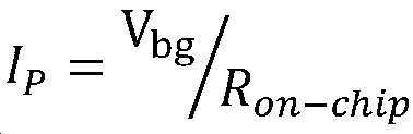
일 예시적인 실시예에서, 교정 회로(200)는 PVT 변동들에 대해 일정한 트랜스컨덕턴스 gMN을 생성하기 위해 전류 I0을 활용할 수 있다. PVT 변동들에 대한 정전류(constant current) I0은 당업계에 알려져 있는 바와 같이 생성될 수 있다. 일 예에서, 정전류 I0은, PVT 변동들에 대해 일정하도록 설계되는 오프-칩(off-chip) 저항 Roff-chip 및 밴드갭 전압 Vbg를 사용하여 생성될 수 있다. 결과적인 전류 I0은 다음과 같다.[0038] In one exemplary embodiment, the

이는 마찬가지로, PVT 변동들에 대해 일정하다. 일 예에서, Kd/Kc 비는 ½로 셋팅될 수 있다. 전류 I0은 50 uA로 셋팅될 수 있다. Kb × Vbg의 값은 50 mV로 셋팅될 수 있다. 이러한 예에서, 트랜스컨덕턴스 gMN은 0.5 m이고, PVT 변동들에 대해 일정한 값이다.This is likewise constant for PVT variations. In one example, the ratio K d / K c can be set to ½. Current I 0 may be set as 50 uA. The value of K b × V bg can be set to 50 mV. In this example, the transconductance g MN is 0.5 m and is a constant value for the PVT variations.
[0039]
일 예시적인 실시예에서, 전류 I0은 PVT 변동들에 대해 보상되지 않도록 생성될 수 있다(예컨대, 전류 I0이 PVT 변동들에 따라 변함). Ron-chip의 저항이 PVT 변동들에 따라 변하므로, 트랜스컨덕턴스 gMN(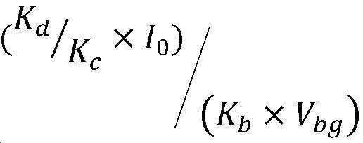
![]()
![]()
여기서, 부하 저항기 RL은 도 1의 저항기들 R1 또는 R2일 수 있고, 저항 Ron-chip의 부분이도록 설계될 수 있다. 따라서, IP × RL은 PVT 변동들에 대해 상수일 수 있다. 이득(110)은 추가로, 다음과 같이 설명될 수 있다.Here, the load resistor R L may be the resistors R 1 or R 2 of FIG. 1 and may be designed to be a part of the resistor R on-chip . Thus, I P x R L may be a constant for PVT variations. The

[0040]
RL의 값은 저항 Ron-chip에 비례할 수 있다. IP의 값이 Ron-chip에 기초하므로, 그에 따라, IP × RL의 값은 PVT 변동들에 대해 일정할 수 있다. 따라서, 이득이 전류 IP에 비례함을 gain110의 일 양상이 제공한다. 위에 나타낸 바와 같이, CML 버퍼(110)의 타겟 이득 gain110은 PVT 변동들에 대해 상수로 교정될 수 있다. 일 예에서, Kb/Kc의 비는 1/2로 셋팅될 수 있다. IP × RL의 값은 200 mV로 셋팅될 수 있다. VIN(예컨대, Kb × Vbg)은 50 mV로 셋팅될 수 있다. 이러한 예에서, gain110은 6 dB이고, PVT 변동들에 대해 일정하다.[0040] The value of R L may be proportional to the resistance R on-chip . The value of I P is based on the R on-chip , so that the value of I P x R L can be constant for PVT variations. Thus, one aspect of gain 110 provides that the gain is proportional to the current I P. As indicated above, the target gain gain 110 of the
[0041]
도 3은, 교정 회로(200)의 예시적인 실시예의 동작들의 흐름도(300)이다. 302에서, 기준 신호가 생성된다. 304에서, 적어도 하나의 차동 회로는 기준 신호에 기초하여, 프로세스 또는 조건 변동들에 따라, 교정된 트랜스컨덕턴스에서 동작한다. 도 1을 참조하면, CML 버퍼(110) 및 CTLE(120)는, 각각이 차동 쌍의 트랜지스터들(각각 112 및 122)을 포함하는 차동 회로들의 예들이다. 도 2 및 연관된 본문을 참조하면, 교정 회로(200)는, 차동 회로들(예컨대, CML 버퍼(110) 및/또는 CTLE(120))에 제공되어 회로들 각각에서 테일 전류를 생성할 수 있는 기준 신호 VREF를 생성하는 회로의 예이다. 차동 회로들 각각은 기준 신호 VREF에 기초하여, PVT 변동들에 따라, 교정된 그리고 일정한 트랜스컨덕턴스에서 동작한다. 교정 회로(200)는 제 1 기준 전류 IP 및 제 2 기준 전류 I0에 기초하여 기준 신호 VREF를 생성할 수 있다. 기준 신호 VREF는 교정 회로에 피드백되어 출력을 계속해서 조정할 수 있다. 교정 회로(200)는, 기준 신호 VREF를 생성하는데 있어 어떠한 피드백도 수신하지 않으며, 그에 따라, 차동 회로들의 동작들과 독립적이다.[0041] FIG. 3 is a
[0042]
306에서, 기준 신호는 기준 신호의 피드백에 기초하여 조정된다. 교정 회로(200)는, 기준 신호의 피드백에 기초한 OTA(210)의 동작들에 의해 기준 신호 VREF를 조정할 수 있다. 도 2 및 연관된 본문을 참조하면, OTA(210)의 트랜지스터 MN29는 기준 신호 VREF의 피드백을 수신하고, 차동 쌍의 트랜지스터들 MN21 및 MN22를 통해 흐르는 테일 전류 ITAIL210을 생성한다. OTA(210)는 OTA(210)의 트랜스컨덕턴스에 기초하여 출력들 I21 및 I22를 생성하는데, 이는 결국, 전술된 테일 전류 ITAIL210에 기초한다.[0042] At 306, the reference signal is adjusted based on the feedback of the reference signal. The
[0043]
일 예에서, 교정 회로(200)는 제 1 기준 전류 (예컨대, IP) 및 제 2 기준 전류(예컨대, I1)에 기초하여 기준 신호 VREF를 생성할 수 있다. 308에서, 기준 전류는 기준 전압으로 변환될 수 있다. 도 2 및 연관된 본문을 참조하면, 교정 회로(200)는 전류 IP(예컨대, 기준 전류 또는 제 1 기준 전류)를 OTA(210)에 입력 전압으로서 제공되는 전압 VIN(예컨대, 기준 전압)으로 변환하기 위해 저항기 Rb를 활용한다. 310에서, 출력은 기준 전압에 기초하여 OTA에 의해 생성될 수 있다. 도 2 및 연관된 본문을 참조하면, OTA(210)는 전압 VIN에 기초하여 출력들 I21 및 I22를 생성한다.[0043] In one example, the
[0044]
312에서, 기준 전압은 프로세스 또는 조건 변동들에 대해 일정하게 유지될 수 있다. 도 2 및 연관된 본문을 참조하면, 전류 소스(212)는 전류 IP를 제공하고, 전류 IP 및 저항기 Rb의 저항에 기초하여 전압 VIN이 생성된다. 전류 IP는, 예를 들어, 교정 회로(200)와 오프 칩으로 로케이팅되는 밴드갭 전압(Vbg) 공급부로부터 생성될 수 있다. 이러한 예는 단지 설명을 위해 제공되며, 본 개시내용의 범위는 분명히 이에 제한되지 않는다. 당업계에 알려져 있는 바와 같이, 밴드갭 전압 Vbg는 PVT 변동들에 대해 일정하다. 이러한 예에서, 전류 IP는 다음과 같이 설명될 수 있다.[0044] At 312, the reference voltage may be held constant for process or condition variations. Referring to FIG. 2 and associated text, the
여기서, 저항 Ron-chip은 저항의 온-칩 부분이며, 저항기 Rb를 포함한다. 저항기 Rb의 저항이 PVT 변동들에 영향을 받으므로, 전류 IP가 마찬가지로 PVT 변동들에 따라 변한다. 저항기 Rb는 총 저항 Ron-chip의 비(예컨대, 그 일부)로서 제공될 수 있다. 따라서, 저항기 Rb의 저항은 다음과 같이 표현될 수 있다.Here, the resistor R on-chip is the on-chip part of the resistor and includes the resistor R b . Since the resistance of resistor R b is affected by PVT variations, the current I P similarly varies with PVT variations. The resistor R b may be provided as a ratio of the total resistance R on-chip (e.g., part thereof). Therefore, the resistance of the resistor R b can be expressed as follows.
![]()
![]()
여기서, Kb는 상수(예컨대, Rb 대 Ron-chip의 비)이다.Where K b is a constant (e.g., R b versus R on-chip ).
따라서, 전압 VIN은 IP × Rb로서 표현되거나 또는 (위에 나타낸 IP 및 Rb에 대한 표현을 치환하여) 다음과 같이 표현될 수 있다.Thus, the voltage V IN may be expressed as I P x R b or alternatively (replacing the expressions for I P and R b shown above) as:
![]()
![]()
따라서, 전압 VIN은 PVT 변동들에 대해 일정하게 유지될 수 있다.Thus, the voltage V IN can be kept constant for PVT variations.
[0045]
(314)에서, OTA의 출력에 기초한 전압과 제 2 기준 전압이 비교될 수 있다. 도 2 및 연관된 본문을 참조하면, 연산 증폭기(220)는 전압 V1을 (제 2) 기준 전압 V0과 비교하고, 출력으로서 기준 신호 VREF를 생성한다. 전압 V1은, 전류 I21 및 전류 I22에 기초하여 (그리고 그에 따라, OTA(210)의 출력들에 기초하여) 생성된다. 일 예에서, 제 2 기준 전압(예컨대, 전압 V0)은, 프로세스 또는 조건 변동들에 대해 일정할 수 있는 제 2 기준 전류(예컨대, 전류 I0)에 기초할 수 있다.[0045] At 314, the voltage based on the output of the OTA and the second reference voltage can be compared. Referring to FIG. 2 and the associated text, the
[0046]
흐름도(300)와 관련하여 설명되는 프로세스는 적어도 하나의 차동 회로가 교정된 이득에서 동작하는 경우에 적용될 수 있다(예컨대, 단계(304)는, 적어도 하나의 차동 회로가, 기준 신호에 기초하여, 프로세스 또는 조건 변동들에 따라, 교정된 이득에서 동작함을 제공함). 교정된 이득에서 적어도 하나의 차동 회로를 동작시키는데 적용되는 경우, 제 2 기준 전류(예컨대, 전류 I0)는 프로세스 또는 조건 변동들에 대해 일정할 필요가 없다(314).The process described in connection with the
[0047]
도 4는, 교정 회로(200)의 다른 예시적인 실시예의 동작들의 흐름도(400)이다. 402에서, 기준 신호가 생성된다. 404에서, 적어도 하나의 차동 회로는 기준 신호에 기초하여, 프로세스 또는 조건 변동들에 따라, 교정된 트랜스컨덕턴스에서 동작한다. 도 1을 참조하면, CML 버퍼(110) 및 CTLE(120)는, 각각이 차동 쌍의 트랜지스터들(각각 112 및 122)을 포함하는 차동 회로들의 예들이다. 도 2 및 연관된 본문을 참조하면, 교정 회로(200)는, 차동 회로들(예컨대, CML 버퍼(110) 및/또는 CTLE(120))에 제공되어 회로들 각각에서 테일 전류를 생성할 수 있는 기준 신호 VREF를 생성하는 회로의 예이다. 차동 회로들 각각은 기준 신호 VREF에 기초하여, PVT 변동들에 따라, 교정된 그리고 일정한 트랜스컨덕턴스에서 동작한다. 교정 회로(200)는 제 1 기준 전류 IP 및 제 2 기준 전류 I0에 기초하여 기준 신호 VREF를 생성할 수 있다. 기준 신호 VREF는 교정 회로에 피드백되어 출력을 계속해서 조정할 수 있다. 교정 회로(200)는, 기준 신호 VREF를 생성하는데 있어 어떠한 피드백도 수신하지 않으며, 그에 따라, 차동 회로들의 동작들과 독립적이다.[0047] FIG. 4 is a flow diagram 400 of operations of another exemplary embodiment of the
[0048]
406에서, 기준 신호는 기준 신호의 피드백에 기초하여 조정된다. 교정 회로(200)는, 기준 신호의 피드백에 기초한 OTA(210)의 동작들에 의해 기준 신호 VREF를 조정할 수 있다. 도 2 및 연관된 본문을 참조하면, OTA(210)의 트랜지스터 MN29는 기준 신호 VREF의 피드백을 수신하고, 차동 쌍의 트랜지스터들 MN21 및 MN22를 통해 흐르는 테일 전류 ITAIL210을 생성한다. OTA(210)는 OTA(210)의 트랜스컨덕턴스에 기초하여 출력들 I21 및 I22를 생성하는데, 이는 결국, 전술된 테일 전류 ITAIL210에 기초한다.[0048] At 406, the reference signal is adjusted based on the feedback of the reference signal. The
[0049]
일 예에서, 교정 회로(200)는 기준 전압 VIN에 기초하여 기준 신호 VREF를 생성할 수 있는데, 이는 결국, 기준 전류(예컨대, IP)에 기초하여 생성된다. 도 2 및 연관된 본문을 참조하면, 교정 회로(200)는 전류 IP(예컨대, 기준 전류 또는 제 1 기준 전류)를 OTA(210)에 입력 전압으로서 제공되는 전압 VIN(예컨대, 기준 전압)으로 변환하기 위해 저항기 Rb를 활용한다. OTA(210)는 전압 VIN에 기초하여 출력들 I21 및 I22를 생성한다.[0049] In one example, the
[0050]
412에서, 기준 전압은 프로세스 또는 조건 변동들에 대해 일정하게 유지될 수 있다. 도 2 및 연관된 본문을 참조하면, 전류 소스(212)는 전류 IP를 제공하고, 전류 IP 및 저항기 Rb의 저항에 기초하여 전압 VIN이 생성된다. 전류 IP는, 예를 들어, 교정 회로(200)와 오프 칩으로 로케이팅되는 밴드갭 전압(Vbg) 공급부로부터 생성될 수 있다. 이러한 예는 단지 설명을 위해 제공되며, 본 개시내용의 범위는 분명히 이에 제한되지 않는다. 당업계에 알려져 있는 바와 같이, 밴드갭 전압 Vbg는 PVT 변동들에 대해 일정하다. 이러한 예에서, 전류 IP는 다음과 같이 설명될 수 있다.[0050] At 412, the reference voltage may be held constant for process or condition variations. Referring to FIG. 2 and associated text, the
여기서, 저항 Ron-chip은 저항의 온-칩 부분이며, 저항기 Rb를 포함한다. 저항기 Rb의 저항이 PVT 변동들에 영향을 받으므로, 전류 IP가 마찬가지로 PVT 변동들에 따라 변한다. 저항기 Rb는 총 저항 Ron-chip의 비(예컨대, 그 일부)로서 제공될 수 있다. 따라서, 저항기 Rb의 저항은 다음과 같이 표현될 수 있다.Here, the resistor R on-chip is the on-chip part of the resistor and includes the resistor R b . Since the resistance of resistor R b is affected by PVT variations, the current I P similarly varies with PVT variations. The resistor R b may be provided as a ratio of the total resistance R on-chip (e.g., part thereof). Therefore, the resistance of the resistor R b can be expressed as follows.
![]()
![]()
여기서, Kb는 상수(예컨대, Rb 대 Ron-chip의 비)이다.Where K b is a constant (e.g., R b versus R on-chip ).
따라서, 전압 VIN은 IP × Rb로서 표현되거나 또는 (위에 나타낸 IP 및 Rb에 대한 표현을 치환하여) 다음과 같이 표현될 수 있다.Thus, the voltage V IN may be expressed as I P x R b or alternatively (replacing the expressions for I P and R b shown above) as:
![]()
![]()
따라서, 전압 VIN은 PVT 변동들에 대해 일정하게 유지될 수 있다.Thus, the voltage V IN can be kept constant for PVT variations.
[0051]
흐름도(400)와 관련하여 설명되는 프로세스는 적어도 하나의 차동 회로가 교정된 트랜스컨덕턴스에서 동작하는 경우에 적용될 수 있다(예컨대, 단계(304)는, 적어도 하나의 차동 회로가, 기준 신호에 기초하여, 프로세스 또는 조건 변동들에 따라, 교정된 트랜스컨덕턴스에서 동작함을 제공함).[0051]
The process described in connection with the
[0052] 개시된 프로세스들의 단계들의 특정 순서 또는 계층 구조는 예시적인 접근법들의 예시라는 것을 이해한다. 설계 선호도들을 기초하여, 프로세스들의 단계들의 특정 순서 또는 계층 구조는 재배열될 수도 있음을 이해한다. 추가로, 몇몇 단계들은 결합되거나 또는 생략될 수 있다. 첨부한 방법 청구항들은 다양한 단계들의 엘리먼트들을 예시적인 순서로 제시하며, 제시된 특정 순서 또는 계층 구조로 한정되는 것으로 여겨지는 것은 아니다. 본원에서 개시된 방법들은 설명된 방법을 달성하기 위한 하나 또는 그 초과의 단계들 또는 동작들을 포함한다. 방법 단계들 및/또는 동작들은 청구항들의 범위를 벗어나지 않으면서 서로 상호교환될 수 있다. 즉, 단계들 또는 동작들의 특정한 순서가 특정되지 않으면, 특정 단계들 및/또는 동작들의 순서 및/또는 사용은 청구항들의 범위를 벗어나지 않으면서 수정될 수 있다. 예를 들어, 단계들은, 본원에 설명된 기능들을 수행하기 위한 회로들 및/또는 본원에 설명된 기능들에 대한 신호들을 생성하는 회로들, 또는 이들의 결합들에 의해 구현될 수 있다.[0052] It is understood that the particular order or hierarchy of steps of the disclosed processes is exemplary of exemplary approaches. It will be appreciated that, based on design preferences, the particular order or hierarchy of steps of the processes may be rearranged. Additionally, some steps may be combined or omitted. The appended method claims present elements of the various steps in an exemplary order and are not intended to be limited to the specific order or hierarchy presented. The methods disclosed herein include one or more steps or operations for achieving the described method. The method steps and / or operations may be interchanged with one another without departing from the scope of the claims. That is, the order and / or use of certain steps and / or operations may be modified without departing from the scope of the claims, unless a specific order of steps or acts is specified. For example, the steps may be implemented by circuits for performing the functions described herein and / or circuits for generating signals for the functions described herein, or combinations thereof.
[0053] 이전의 설명은 임의의 당업자가 본원에 설명된 다양한 양상들을 실시할 수 있도록 제공된다. 이들 양상들에 대한 다양한 수정들이 당업자들에게는 용이하게 명백할 것이며, 본원에 정의된 일반적인 원리들은 다른 양상들에 적용될 수 있다. 따라서, 청구항들은 본원에 설명된 양상들로 제한되도록 의도되는 것이 아니라, 청구항들의 문언에 부합하는 최대 범위를 부여하려는 것이며, 여기서, 단수형의 엘리먼트에 대한 참조는 구체적으로 그렇게 나타내지 않으면 "하나 및 오직 하나"를 의미하기보다는 오히려 "하나 또는 그 초과"를 의미하도록 의도된다. 달리 구체적으로 나타내지 않으면, 용어 "몇몇"은 하나 또는 그 초과를 지칭한다. 당업자들에게 알려져 있거나 추후에 알려지게 될 본 개시내용 전반에 걸쳐 설명된 다양한 양상들의 엘리먼트들에 대한 모든 구조적 및 기능적 균등물들은, 인용에 의해 본원에 명백히 포함되고, 청구항들에 의해 포함되도록 의도된다. 또한, 본원에 개시된 어떠한 것도, 청구항들에 이러한 개시내용이 명시적으로 언급되어 있는지 여부와 관계없이, 공중이 사용하도록 의도되는 것은 아니다. "~을 위한 수단" 문구를 사용하여 청구항 엘리먼트가 명백히 언급되거나 또는 방법 청구항의 경우에, "~을 위한 단계" 문구를 사용하여 청구항 엘리먼트가 언급되지 않는 한, 어떠한 청구항 엘리먼트도 35 U.S.C.§112(f)의 조항들에 따라 해석되지 않아야 한다.[0053] The previous description is provided to enable any person skilled in the art to practice the various aspects described herein. Various modifications to these aspects will be readily apparent to those skilled in the art, and the generic principles defined herein may be applied to other aspects. Accordingly, the claims are not intended to be limited to the aspects described herein but are to be accorded the widest scope consistent with the language of the claims, where references to singular elements, unless specifically so indicated, "Quot; is intended to mean " one or more. &Quot; Unless specifically stated otherwise, the term " some " refers to one or more. All structural and functional equivalents to elements of the various aspects described throughout this disclosure which are known or later known to those skilled in the art are expressly incorporated herein by reference and are intended to be encompassed by the claims. Furthermore, nothing disclosed herein is intended for public use, whether or not such disclosure is expressly referred to in the claims. Unless a claim element is expressly referred to using the phrase " means for " or, in the case of a method claim, the claim element is referred to using the phrase " for step " shall not be construed in accordance with the provisions of subsection (f).
Claims (22)
기준 신호를 생성하도록 구성되는 교정(calibration) 회로; 및
적어도 하나의 차동 회로를 포함하며,
상기 적어도 하나의 차동 회로 각각은, 상기 기준 신호에 기초하여, 프로세스 또는 조건 변동들에 대해, 교정된 트랜스컨덕턴스(transconductance)에서 동작하도록 구성되고,
상기 교정 회로는 추가로, 상기 적어도 하나의 차동 회로와는 독립적으로 상기 기준 신호를 생성하고, 상기 기준 신호의 피드백을 제공하고, 그리고 상기 피드백에 기초하여 상기 기준 신호를 조정하도록 구성되고,
상기 교정 회로는, 상기 피드백에 기초하여 테일(tail) 전류를 생성하도록 구성되는 OTA(operational transconductance amplifier)를 더 포함하며, 그리고
상기 교정 회로는, 상기 OTA의 출력에 기초한 전압과 제 2 기준 전압을 비교하도록 구성되는 연산 증폭기를 더 포함하고,
상기 교정 회로는, 상기 비교에 기초하여 상기 기준 신호를 생성하도록 구성되는, 장치.As an apparatus,
A calibration circuit configured to generate a reference signal; And
At least one differential circuit,
Wherein each of the at least one differential circuit is configured to operate in a calibrated transconductance for process or condition variations based on the reference signal,
Wherein the calibration circuit is further configured to generate the reference signal independently of the at least one differential circuit, provide feedback of the reference signal, and adjust the reference signal based on the feedback,
The calibration circuit further comprises an operational transconductance amplifier (OTA) configured to generate a tail current based on the feedback,
Wherein the calibration circuit further comprises an operational amplifier configured to compare a voltage based on an output of the OTA with a second reference voltage,
Wherein the calibration circuit is configured to generate the reference signal based on the comparison.
상기 적어도 하나의 차동 회로 각각은 차동 쌍의 트랜지스터들을 포함하고,
상기 적어도 하나의 차동 회로 각각은 추가로, 상기 기준 신호에 기초하여, 상기 적어도 하나의 차동 회로 각각의 개별적인 차동 쌍의 트랜지스터들에 대한 테일 전류를 생성하도록 구성되는, 장치.The method according to claim 1,
Each of said at least one differential circuit comprising a differential pair of transistors,
Wherein each of the at least one differential circuit is further configured to generate a tail current for the transistors of the respective differential pair of each of the at least one differential circuit based on the reference signal.
상기 교정 회로는 추가로, 제 1 기준 전류 및 제 2 기준 전류에 기초하여 상기 기준 신호를 생성하도록 구성되는, 장치.The method according to claim 1,
Wherein the calibration circuit is further configured to generate the reference signal based on a first reference current and a second reference current.
상기 교정 회로는 기준 전류를 기준 전압으로 변환하도록 구성되는 회로를 더 포함하고,
상기 OTA는 추가로, 상기 기준 전압에 기초하여 출력을 생성하도록 구성되는, 장치.The method according to claim 1,
Wherein the calibration circuit further comprises circuitry configured to convert the reference current to a reference voltage,
Wherein the OTA is further configured to generate an output based on the reference voltage.
상기 교정 회로는 추가로, 상기 프로세스 또는 조건 변동들에 대해 상기 기준 전압을 일정하게 유지하도록 구성되는, 장치.5. The method of claim 4,
Wherein the calibration circuit is further configured to maintain the reference voltage constant for the process or condition variations.
상기 제 2 기준 전압은 제 2 기준 전류에 기초하고, 그리고
상기 제 2 기준 전류는 상기 프로세스 또는 조건 변동들에 대해 일정한, 장치.The method according to claim 1,
The second reference voltage is based on a second reference current, and
Wherein the second reference current is constant for the process or condition variations.
기준 신호를 생성하는 단계;
상기 기준 신호에 기초하여, 프로세스 또는 조건 변동들에 대해, 상기 적어도 하나의 차동 회로를 교정된 트랜스컨덕턴스에서 동작시키는 단계; 및
상기 기준 신호의 피드백에 기초하여 상기 기준 신호를 조정하는 단계를 포함하며,
상기 기준 신호는 상기 적어도 하나의 차동 회로와는 독립적으로 생성되고,
상기 기준 신호는 상기 피드백에 기초한 테일 전류를 갖는 OTA(operational transconductance amplifier)를 사용하여 생성되고,
상기 기준 신호를 생성하는 단계는, 상기 OTA의 출력에 기초한 전압과 제 2 기준 전압을 비교하는 단계를 더 포함하며,
상기 기준 신호는 상기 비교에 기초하는, 적어도 하나의 차동 회로를 동작시키기 위한 방법.CLAIMS 1. A method for operating at least one differential circuit,
Generating a reference signal;
Operating the at least one differential circuit at a calibrated transconductance for process or condition variations based on the reference signal; And
And adjusting the reference signal based on feedback of the reference signal,
Wherein the reference signal is generated independently of the at least one differential circuit,
Wherein the reference signal is generated using an operational transconductance amplifier (OTA) having a tail current based on the feedback,
Wherein generating the reference signal further comprises comparing a voltage based on an output of the OTA with a second reference voltage,
Wherein the reference signal is based on the comparison.
상기 적어도 하나의 차동 회로 각각은 차동 쌍의 트랜지스터들을 포함하고,
상기 적어도 하나의 차동 회로는, 상기 기준 신호에 기초한, 상기 차동 쌍의 트랜지스터들에 통하는 테일 전류로 동작되는, 적어도 하나의 차동 회로를 동작시키기 위한 방법.8. The method of claim 7,
Each of said at least one differential circuit comprising a differential pair of transistors,
Wherein the at least one differential circuit is operated with a tail current through the transistors of the differential pair based on the reference signal.
상기 기준 신호는 제 1 기준 전류 및 제 2 기준 전류에 기초하여 생성되는, 적어도 하나의 차동 회로를 동작시키기 위한 방법.8. The method of claim 7,
Wherein the reference signal is generated based on a first reference current and a second reference current.
상기 기준 신호를 생성하는 단계는,
기준 전류를 기준 전압으로 변환하는 단계; 및
상기 기준 전압에 기초하여 상기 OTA에 의해 출력을 생성하는 단계
를 더 포함하는, 적어도 하나의 차동 회로를 동작시키기 위한 방법.8. The method of claim 7,
Wherein the step of generating the reference signal comprises:
Converting the reference current to a reference voltage; And
Generating an output by the OTA based on the reference voltage
≪ / RTI > further comprising the step of:
상기 기준 신호를 생성하는 단계는, 상기 프로세스 또는 조건 변동들에 대해 상기 기준 전압을 일정하게 유지하는 단계를 더 포함하는, 적어도 하나의 차동 회로를 동작시키기 위한 방법.11. The method of claim 10,
Wherein generating the reference signal further comprises maintaining the reference voltage constant for the process or condition variations. ≪ Desc / Clms Page number 21 >
상기 제 2 기준 전압은 제 2 기준 전류에 기초하고,
상기 제 2 기준 전류는 상기 프로세스 또는 조건 변동들에 대해 일정한, 적어도 하나의 차동 회로를 동작시키기 위한 방법.8. The method of claim 7,
Wherein the second reference voltage is based on a second reference current,
Wherein the second reference current is constant for the process or condition variations.
기준 신호를 생성하도록 구성되는 교정 회로; 및
적어도 2개의 타입들의 차동 회로들을 포함하며,
상기 적어도 2개의 타입들의 차동 회로들 각각은, 상기 기준 신호에 기초하여, 프로세스 또는 조건 변동들에 대해, 교정된 이득에서 동작하도록 구성되고,
상기 적어도 2개의 타입들의 차동 회로들은, 버퍼 회로, 및 필터를 포함하는 CTLE(continuous time linear equalizer) 회로를 포함하고, 상기 CTLE 회로는 상기 버퍼 회로의 출력을 수신하고 그리고 등화된(equalized) 출력을 제공하도록 구성되며,
상기 교정 회로는 상기 적어도 2개의 타입들의 차동 회로들로부터 피드백을 수신하지 않고 상기 기준 신호를 생성하도록 구성되는, 장치.As an apparatus,
A calibration circuit configured to generate a reference signal; And
Comprising at least two types of differential circuits,
Wherein each of the at least two types of differential circuits is configured to operate at a calibrated gain for process or condition variations based on the reference signal,
Wherein the at least two types of differential circuits comprise a buffer circuit and a continuous time linear equalizer (CTLE) circuit comprising a filter, the CTLE circuit receiving the output of the buffer circuit and providing an equalized output Lt; / RTI >
Wherein the calibration circuit is configured to generate the reference signal without receiving feedback from the at least two types of differential circuits.
상기 적어도 2개의 타입들의 차동 회로들 각각은 차동 쌍의 트랜지스터들을 포함하고, 그리고 상기 기준 신호에 기초하여 상기 차동 쌍의 트랜지스터들에 대한 테일 전류를 생성하도록 추가적으로 구성되는, 장치.14. The method of claim 13,
Wherein each of the at least two types of differential circuits comprises a differential pair of transistors and is further configured to generate a tail current for the transistors of the differential pair based on the reference signal.
상기 교정 회로는 추가로, 상기 기준 신호를 피드백하고 그리고 상기 피드백에 기초하여 상기 기준 신호를 조정하도록 구성되는, 장치.14. The method of claim 13,
Wherein the calibration circuit is further configured to feedback the reference signal and adjust the reference signal based on the feedback.
상기 교정 회로는 추가로, 기준 전압에 기초하여 상기 기준 신호를 생성하고 그리고 상기 프로세스 또는 조건 변동들에 대해 상기 기준 전압을 일정하게 유지하도록 구성되는, 장치.14. The method of claim 13,
Wherein the calibration circuit is further configured to generate the reference signal based on the reference voltage and to maintain the reference voltage constant for the process or condition variations.
기준 전압에 기초하여 기준 신호를 생성하고 그리고 프로세스 또는 조건 변동들에 대해 상기 기준 전압을 일정하게 유지하도록 구성되는 교정 회로; 및
적어도 2개의 타입들의 차동 회로들을 포함하며,
상기 적어도 2개의 타입들의 차동 회로들 각각은, 상기 기준 신호에 기초하여, 상기 프로세스 또는 조건 변동들에 대해, 교정된 이득에서 동작하도록 구성되고,
상기 적어도 2개의 타입들의 차동 회로들은, 버퍼 회로 및 상기 버퍼 회로의 출력을 수신하도록 구성된 차동 회로를 포함하고,
상기 교정 회로는 상기 적어도 2개의 타입들의 차동 회로들로부터 피드백을 수신하지 않고 상기 기준 신호를 생성하도록 구성되며,
상기 기준 전압은 기준 전류에 기초하고,
상기 교정된 이득은 상기 기준 전류에 비례하는, 장치.As an apparatus,
A calibration circuit configured to generate a reference signal based on the reference voltage and to maintain the reference voltage constant for process or condition variations; And
Comprising at least two types of differential circuits,
Wherein each of the at least two types of differential circuits is configured to operate at a calibrated gain for the process or condition variations based on the reference signal,
Wherein the at least two types of differential circuits comprise a buffer circuit and a differential circuit configured to receive an output of the buffer circuit,
Wherein the calibration circuit is configured to generate the reference signal without receiving feedback from the at least two types of differential circuits,
Wherein the reference voltage is based on a reference current,
Wherein the calibrated gain is proportional to the reference current.
기준 신호를 생성하는 단계;
상기 기준 신호에 기초하여, 프로세스 또는 조건 변동들에 대해, 상기 적어도 2개의 타입들의 차동 회로들을 교정된 이득에서 동작시키는 단계를 포함하며,
상기 적어도 2개의 타입들의 차동 회로들은, 버퍼 회로, 및 필터를 포함하는 CTLE(continuous time linear equalizer) 회로를 포함하고, 상기 CTLE 회로는 상기 버퍼 회로의 출력을 수신하고 그리고 등화된 출력을 제공하도록 구성되며,
상기 기준 신호는 상기 적어도 2개의 타입들의 차동 회로들로부터 피드백을 수신하지 않고 생성되는, 적어도 2개의 타입들의 차동 회로들을 동작시키기 위한 방법.CLAIMS 1. A method for operating at least two types of differential circuits,
Generating a reference signal;
Operating the at least two types of differential circuits at a calibrated gain, for process or condition variations, based on the reference signal,
Wherein the at least two types of differential circuits comprise a buffer circuit and a continuous time linear equalizer (CTLE) circuit comprising a filter, the CTLE circuit configured to receive the output of the buffer circuit and to provide an equalized output And,
Wherein the reference signal is generated without receiving feedback from the at least two types of differential circuits.
상기 적어도 2개의 타입들의 차동 회로들 각각은 차동 쌍의 트랜지스터들을 포함하고, 그리고 상기 기준 신호에 기초한, 상기 차동 쌍의 트랜지스터들에 통하는 테일 전류로 동작되는, 적어도 2개의 타입들의 차동 회로들을 동작시키기 위한 방법.19. The method of claim 18,
Each of said at least two types of differential circuits comprising differential pair of transistors and operating with at least two types of differential circuits based on said reference signal and operating with a tail current through said transistors of said differential pair Way.
상기 기준 신호의 피드백에 기초하여 상기 기준 신호를 조정하는 단계를 더 포함하는, 적어도 2개의 타입들의 차동 회로들을 동작시키기 위한 방법.19. The method of claim 18,
Further comprising adjusting the reference signal based on feedback of the reference signal. ≪ Desc / Clms Page number 21 >
상기 기준 신호를 생성하는 단계는 기준 전압에 기초하고, 상기 프로세스 또는 조건 변동들에 대해 상기 기준 전압을 일정하게 유지하는 단계를 더 포함하는, 적어도 2개의 타입들의 차동 회로들을 동작시키기 위한 방법.19. The method of claim 18,
Wherein generating the reference signal further comprises maintaining the reference voltage constant for the process or condition variations based on the reference voltage. ≪ Desc / Clms Page number 21 >
기준 전압에 기초하여 기준 신호를 생성하는 단계;
프로세스 또는 조건 변동들에 대해 상기 기준 전압을 일정하게 유지하는 단계;
상기 기준 신호에 기초하여, 상기 프로세스 또는 조건 변동들에 대해, 상기 적어도 2개의 타입들의 차동 회로들을 교정된 이득에서 동작시키는 단계를 포함하며,
상기 적어도 2개의 타입들의 차동 회로들은, 버퍼 회로 및 상기 버퍼 회로의 출력을 수신하도록 구성된 차동 회로를 포함하고,
상기 기준 신호는 상기 적어도 2개의 타입들의 차동 회로들로부터 피드백을 수신하지 않고 생성되며,
상기 기준 전압은 기준 전류에 기초하고,
상기 교정된 이득은 상기 기준 전류에 비례하는, 적어도 2개의 타입들의 차동 회로들을 동작시키기 위한 방법.CLAIMS 1. A method for operating at least two types of differential circuits,
Generating a reference signal based on the reference voltage;
Maintaining the reference voltage constant for process or condition variations;
Operating the at least two types of differential circuits at a calibrated gain, for the process or condition variations, based on the reference signal,
Wherein the at least two types of differential circuits comprise a buffer circuit and a differential circuit configured to receive an output of the buffer circuit,
Wherein the reference signal is generated without receiving feedback from the at least two types of differential circuits,
Wherein the reference voltage is based on a reference current,
Wherein the calibrated gain is proportional to the reference current.
Applications Claiming Priority (3)
| Application Number | Priority Date | Filing Date | Title |
|---|---|---|---|
| US14/595,106 US9450540B2 (en) | 2015-01-12 | 2015-01-12 | Methods and apparatus for calibrating for transconductance or gain over process or condition variations in differential circuits |
| US14/595,106 | 2015-01-12 | ||
| PCT/US2015/065358 WO2016114882A1 (en) | 2015-01-12 | 2015-12-11 | Methods and apparatus for calibrating for transconductance or gain over process or condition variations in differential circuits |
Related Parent Applications (1)
| Application Number | Title | Priority Date | Filing Date |
|---|---|---|---|
| KR1020177018228A Division KR20170082642A (en) | 2015-01-12 | 2015-12-11 | Methods and apparatus for calibrating for transconductance or gain over process or condition variations in differential circuits |
Publications (1)
| Publication Number | Publication Date |
|---|---|
| KR20180097779A true KR20180097779A (en) | 2018-08-31 |
Family
ID=55069145
Family Applications (2)
| Application Number | Title | Priority Date | Filing Date |
|---|---|---|---|
| KR1020187024085A Withdrawn KR20180097779A (en) | 2015-01-12 | 2015-12-11 | Methods and apparatus for calibrating for transconductance or gain over process or condition variations in differential circuits |
| KR1020177018228A Ceased KR20170082642A (en) | 2015-01-12 | 2015-12-11 | Methods and apparatus for calibrating for transconductance or gain over process or condition variations in differential circuits |
Family Applications After (1)
| Application Number | Title | Priority Date | Filing Date |
|---|---|---|---|
| KR1020177018228A Ceased KR20170082642A (en) | 2015-01-12 | 2015-12-11 | Methods and apparatus for calibrating for transconductance or gain over process or condition variations in differential circuits |
Country Status (7)
| Country | Link |
|---|---|
| US (1) | US9450540B2 (en) |
| EP (1) | EP3245736B1 (en) |
| JP (1) | JP2018504842A (en) |
| KR (2) | KR20180097779A (en) |
| CN (1) | CN107210716B (en) |
| BR (1) | BR112017014906A2 (en) |
| WO (1) | WO2016114882A1 (en) |
Cited By (1)
| Publication number | Priority date | Publication date | Assignee | Title |
|---|---|---|---|---|
| WO2024195953A1 (en) * | 2023-03-17 | 2024-09-26 | 주식회사 엘엑스세미콘 | Display driving chip |
Families Citing this family (4)
| Publication number | Priority date | Publication date | Assignee | Title |
|---|---|---|---|---|
| US10193507B1 (en) * | 2017-07-31 | 2019-01-29 | Analog Devices Global | Current switching circuit |
| US10680634B1 (en) * | 2019-04-08 | 2020-06-09 | Kandou Labs, S.A. | Dynamic integration time adjustment of a clocked data sampler using a static analog calibration circuit |
| US11469730B2 (en) * | 2019-12-06 | 2022-10-11 | Qualcomm Incorporated | Circuits and methods for maintaining gain for a continuous-time linear equalizer |
| KR102754773B1 (en) * | 2022-03-28 | 2025-01-21 | 주식회사 피델릭스 | Data input buffer for effectively calibrating offset |
Family Cites Families (24)
| Publication number | Priority date | Publication date | Assignee | Title |
|---|---|---|---|---|
| JPH10112614A (en) * | 1996-10-07 | 1998-04-28 | Hitachi Ltd | Bias current supply method and circuit thereof |
| JP3841195B2 (en) | 1998-12-02 | 2006-11-01 | 富士通株式会社 | Differential amplifier |
| TW472985U (en) | 2001-01-05 | 2002-01-11 | Elan Microelectronics Corp | Current-controlled CMOS amplification circuit |
| US6480064B1 (en) | 2001-05-25 | 2002-11-12 | Infineon Technologies Ag | Method and apparatus for an efficient low voltage switchable Gm cell |
| US6737919B2 (en) | 2001-05-25 | 2004-05-18 | Infineon Technologies North America Corp. | Method and apparatus for calibrating a Gm cell utilizing a replica Gm cell |
| US6529077B1 (en) * | 2001-08-22 | 2003-03-04 | Institute Of Microelectronics | Gain compensation circuit for CMOS amplifiers |
| FR2834087A1 (en) * | 2001-12-20 | 2003-06-27 | Koninkl Philips Electronics Nv | Circuit with substantially constant transconductance has means to polarise MOS transistors with current which varies with temperature to compensate the change in mobility of holes and electrons |
| US6753732B1 (en) | 2003-02-10 | 2004-06-22 | Analog Devices, Inc. | Accurate, wide-band, low-noise variable-gain amplifier structures and gain control methods |
| KR101067495B1 (en) * | 2003-05-26 | 2011-09-27 | 페어차일드코리아반도체 주식회사 | Transconductance Control Circuit of Rail-to-Rail Differential Input |
| US20050007160A1 (en) | 2003-07-10 | 2005-01-13 | Neff Robert M. R. | Tunable differential transconductor and adjustment method |
| EP1513253A1 (en) | 2003-09-05 | 2005-03-09 | Semiconductor Ideas to The Market (ItoM) BV | Programmable high precision filter |
| US7196551B2 (en) * | 2004-05-28 | 2007-03-27 | Lattice Semiconductor Corporation | Current mode logic buffer |
| JP4578896B2 (en) | 2004-08-26 | 2010-11-10 | ルネサスエレクトロニクス株式会社 | Clock buffer circuit |
| US8620249B2 (en) | 2004-10-29 | 2013-12-31 | Broadcom Corporation | Method and system for process, voltage, and temperature (PVT) measurement and calibration |
| JP4676885B2 (en) * | 2006-01-04 | 2011-04-27 | 富士通セミコンダクター株式会社 | Bias circuit |
| KR100791934B1 (en) * | 2006-07-24 | 2008-01-04 | 삼성전자주식회사 | High voltage output buffer circuit of high speed signal transmission system |
| CN106508091B (en) * | 2006-08-11 | 2011-06-01 | 中国科学院电子学研究所 | A kind of preposition amplification method of complementary metal oxide semiconductors (CMOS) controllable gain and circuit |
| CN101471632B (en) * | 2007-12-26 | 2011-07-20 | 中国科学院微电子研究所 | A self-biased low-voltage operational transconductance amplifier circuit with controllable loop gain |
| US7843264B2 (en) * | 2008-01-29 | 2010-11-30 | Qualcomm, Incorporated | Differential amplifier with accurate input offset voltage |
| CN102668373B (en) * | 2009-11-30 | 2015-12-16 | 意法半导体股份有限公司 | For obtaining the driving method of the gain linearity change of trsanscondutance amplifier and corresponding drive circuit |
| CN102340284B (en) * | 2010-07-23 | 2014-03-05 | 复旦大学 | A Low Supply Voltage Transconductance Adjustable Constant Transconductance Rail-to-Rail Input Operational Amplifier |
| US20120139638A1 (en) * | 2010-12-03 | 2012-06-07 | Rambus Inc. | Methods and Circuits for Controlling Amplifier Gain Over Process, Voltage, and Temperature |
| CN102723920B (en) * | 2012-07-19 | 2014-11-26 | 电子科技大学 | Transconductance stabilizing circuit of operational amplifiers |
| US8970301B2 (en) * | 2013-05-20 | 2015-03-03 | Analog Devices, Inc. | Method for low power low noise input bias current compensation |
-
2015
- 2015-01-12 US US14/595,106 patent/US9450540B2/en active Active
- 2015-12-11 WO PCT/US2015/065358 patent/WO2016114882A1/en not_active Ceased
- 2015-12-11 KR KR1020187024085A patent/KR20180097779A/en not_active Withdrawn
- 2015-12-11 CN CN201580072655.2A patent/CN107210716B/en active Active
- 2015-12-11 JP JP2017536585A patent/JP2018504842A/en active Pending
- 2015-12-11 KR KR1020177018228A patent/KR20170082642A/en not_active Ceased
- 2015-12-11 BR BR112017014906A patent/BR112017014906A2/en not_active Application Discontinuation
- 2015-12-11 EP EP15819993.5A patent/EP3245736B1/en active Active
Cited By (1)
| Publication number | Priority date | Publication date | Assignee | Title |
|---|---|---|---|---|
| WO2024195953A1 (en) * | 2023-03-17 | 2024-09-26 | 주식회사 엘엑스세미콘 | Display driving chip |
Also Published As
| Publication number | Publication date |
|---|---|
| US20160204749A1 (en) | 2016-07-14 |
| KR20170082642A (en) | 2017-07-14 |
| EP3245736B1 (en) | 2019-07-17 |
| US9450540B2 (en) | 2016-09-20 |
| BR112017014906A2 (en) | 2018-03-13 |
| WO2016114882A1 (en) | 2016-07-21 |
| CN107210716B (en) | 2021-05-28 |
| JP2018504842A (en) | 2018-02-15 |
| EP3245736A1 (en) | 2017-11-22 |
| CN107210716A (en) | 2017-09-26 |
Similar Documents
| Publication | Publication Date | Title |
|---|---|---|
| CN109565278B (en) | Impedance and swing control for voltage mode drivers | |
| JP4858959B2 (en) | Differential signal drive circuit and differential signal drive method | |
| US10038574B2 (en) | Method and apparatus for passive continuous-time linear equalization with continuous-time baseline wander correction | |
| US9746864B1 (en) | Fast transient low drop-out voltage regulator for a voltage-mode driver | |
| US20190140768A1 (en) | Baseline wander correction | |
| KR20180097779A (en) | Methods and apparatus for calibrating for transconductance or gain over process or condition variations in differential circuits | |
| US20070057702A1 (en) | Output buffer circuit | |
| US7109759B2 (en) | Voltage mode current-assisted pre-emphasis driver | |
| US8487700B2 (en) | Pre-driver and digital transmitter using the same | |
| CN102624341B (en) | Differential receiver | |
| JP2008182418A (en) | Semiconductor integrated circuit | |
| JP2005191864A (en) | Receiver | |
| CN114448353B (en) | Analog equalizer | |
| Terzopoulos et al. | A 5‐Gbps USB3. 0 transmitter and receiver linear equalizer | |
| JP2016072719A (en) | Transmission circuit and semiconductor integrated circuit | |
| JP4957405B2 (en) | Signal waveform equalization circuit and reception circuit | |
| JP7705052B2 (en) | Common adjustment circuit | |
| US9608633B1 (en) | Interface circuit with configurable variable supply voltage for transmitting signals | |
| EP1926214B1 (en) | Common-mode voltage controller | |
| US9998120B1 (en) | Circuit for and method of shifting a high range input common mode voltage | |
| CN114788174B (en) | Differential amplifier circuit, receiving circuit, and semiconductor integrated circuit | |
| CN117762847A (en) | LVDS receiving circuit | |
| Buhr et al. | Ultra low power class-AB voltage mode line driver for fast ethernet | |
| Rao et al. | Active‐terminated transmitter and receiver circuits for high‐speed low‐swing duobinary signaling | |
| Kim | Design of a low-power CMOS LVDS I/O interface circuit |
Legal Events
| Date | Code | Title | Description |
|---|---|---|---|
| A107 | Divisional application of patent | ||
| PA0104 | Divisional application for international application |
Comment text: Divisional Application for International Patent Patent event code: PA01041R01D Patent event date: 20180821 Application number text: 1020177018228 Filing date: 20170630 |
|
| PG1501 | Laying open of application | ||
| PC1203 | Withdrawal of no request for examination |