KR20170126810A - Plasma processing apparatus and plasma processing method - Google Patents
Plasma processing apparatus and plasma processing method Download PDFInfo
- Publication number
- KR20170126810A KR20170126810A KR1020170058071A KR20170058071A KR20170126810A KR 20170126810 A KR20170126810 A KR 20170126810A KR 1020170058071 A KR1020170058071 A KR 1020170058071A KR 20170058071 A KR20170058071 A KR 20170058071A KR 20170126810 A KR20170126810 A KR 20170126810A
- Authority
- KR
- South Korea
- Prior art keywords
- carrier wave
- carrier
- group
- peak portion
- waveform data
- Prior art date
- Legal status (The legal status is an assumption and is not a legal conclusion. Google has not performed a legal analysis and makes no representation as to the accuracy of the status listed.)
- Granted
Links
Images


Classifications
-
- H—ELECTRICITY
- H01—ELECTRIC ELEMENTS
- H01J—ELECTRIC DISCHARGE TUBES OR DISCHARGE LAMPS
- H01J37/00—Discharge tubes with provision for introducing objects or material to be exposed to the discharge, e.g. for the purpose of examination or processing thereof
- H01J37/32—Gas-filled discharge tubes
- H01J37/32009—Arrangements for generation of plasma specially adapted for examination or treatment of objects, e.g. plasma sources
- H01J37/32082—Radio frequency generated discharge
- H01J37/32174—Circuits specially adapted for controlling the RF discharge
-
- H—ELECTRICITY
- H01—ELECTRIC ELEMENTS
- H01J—ELECTRIC DISCHARGE TUBES OR DISCHARGE LAMPS
- H01J37/00—Discharge tubes with provision for introducing objects or material to be exposed to the discharge, e.g. for the purpose of examination or processing thereof
- H01J37/32—Gas-filled discharge tubes
- H01J37/32009—Arrangements for generation of plasma specially adapted for examination or treatment of objects, e.g. plasma sources
- H01J37/32192—Microwave generated discharge
-
- H—ELECTRICITY
- H01—ELECTRIC ELEMENTS
- H01J—ELECTRIC DISCHARGE TUBES OR DISCHARGE LAMPS
- H01J37/00—Discharge tubes with provision for introducing objects or material to be exposed to the discharge, e.g. for the purpose of examination or processing thereof
- H01J37/32—Gas-filled discharge tubes
- H01J37/32009—Arrangements for generation of plasma specially adapted for examination or treatment of objects, e.g. plasma sources
- H01J37/32082—Radio frequency generated discharge
- H01J37/32091—Radio frequency generated discharge the radio frequency energy being capacitively coupled to the plasma
-
- H—ELECTRICITY
- H01—ELECTRIC ELEMENTS
- H01J—ELECTRIC DISCHARGE TUBES OR DISCHARGE LAMPS
- H01J37/00—Discharge tubes with provision for introducing objects or material to be exposed to the discharge, e.g. for the purpose of examination or processing thereof
- H01J37/32—Gas-filled discharge tubes
- H01J37/32009—Arrangements for generation of plasma specially adapted for examination or treatment of objects, e.g. plasma sources
- H01J37/32192—Microwave generated discharge
- H01J37/32266—Means for controlling power transmitted to the plasma
-
- H10P50/242—
Landscapes
- Physics & Mathematics (AREA)
- Engineering & Computer Science (AREA)
- Plasma & Fusion (AREA)
- Chemical & Material Sciences (AREA)
- Analytical Chemistry (AREA)
- Plasma Technology (AREA)
- Drying Of Semiconductors (AREA)
Abstract
Description
본 발명의 다양한 측면 및 실시 형태는 플라즈마 처리 장치 및 플라즈마 처리 방법에 관한 것이다.Various aspects and embodiments of the present invention are directed to a plasma processing apparatus and a plasma processing method.
종래, 고주파 전원에 의해 생성되는 고주파 전력을 이용해서 처리 용기 내에 플라즈마를 생성하는 플라즈마 처리 장치가 알려져 있다. 또, 주파수가 상이한 복수의 고주파 전력을 복수의 고주파 전원에 의해 생성하는 기술도 있다.2. Description of the Related Art Conventionally, a plasma processing apparatus for generating plasma in a processing vessel using high-frequency power generated by a high-frequency power source is known. There is also a technique in which a plurality of high-frequency powers having different frequencies are generated by a plurality of high-frequency power sources.
그렇지만, 고주파 전원에 의해 생성되는 고주파 전력을 이용해서 처리 용기 내에 플라즈마를 생성하는 경우, 저압 또한 저플라즈마 밀도의 환경하에서 플라즈마를 안정적으로 유지하는 것이 곤란하다고 하는 문제가 있다. 예를 들면, 저압의 환경하에서 플라즈마를 유지하기 위해서는, 고주파 전원에 의해 생성되는 고주파 전력을 증가시키는 것이 생각된다. 고주파 전력이 증가되면, 처리 용기 내의 전계가 증대하므로, 플라즈마의 전리(電離)가 가속되고, 플라즈마 밀도가 과도하게 증가해 버릴 우려가 있다.However, there is a problem that it is difficult to stably maintain the plasma under an environment of low pressure and low plasma density when plasma is generated in the processing vessel by using the high frequency power generated by the high frequency power source. For example, in order to maintain the plasma under a low-pressure environment, it is considered to increase the high-frequency power generated by the high-frequency power source. When the high frequency electric power is increased, the electric field in the processing vessel is increased, so that the ionization of the plasma is accelerated and the plasma density is excessively increased.
한편, 플라즈마 밀도의 과도한 증가를 억제하기 위해서, 플라즈마의 생성(착화) 후에, 고주파 전력을 플라즈마의 생성(착화) 시의 값보다 작은 값으로 감소시키는 것이 생각된다. 그렇지만, 고주파 전력을 감소시킨 경우, 처리 용기 내의 전계가 저하하므로, 플라즈마를 유지하기 위해서 충분한 전계가 확보되지 않아, 플라즈마가 소멸하게 될 우려가 있다. 이 점에서, 종래의 CCP(Capacitively Coupled Plasma)형 플라즈마 장치로 높은 이온 에너지를 얻기 위해서는, 주파수를 저주파로 할 필요가 있었지만, 반면, 이온 에너지 분포가 크게 넓어져서, 이온 에너지의 분포를 억제해 정확히 이온 에너지를 제어하는 것은 곤란했다.On the other hand, in order to suppress an excessive increase in the plasma density, it is conceivable that after generation of plasma (ignition), the high-frequency power is reduced to a value smaller than the value at the generation (ignition) of the plasma. However, when the high frequency power is reduced, the electric field in the processing container is lowered, so that an electric field sufficient for holding the plasma can not be ensured and the plasma may be destroyed. In this regard, in order to obtain a high ion energy by a conventional CCP (Capacitively Coupled Plasma) type plasma apparatus, it has been necessary to set the frequency to a low frequency. On the other hand, the ion energy distribution is greatly widened, It was difficult to control the ion energy.
개시하는 플라즈마 처리 장치는 1개의 실시 형태에 있어서, 처리 용기와, 주파수 영역에 있어 주파수가 상이한 복수의 반송파로부터 이루어지는 반송파군으로서, 시간 영역에 있어서 제 1 피크 부분과 상기 제 1 피크 부분보다 절대치가 작은 제 2 피크 부분이 교대로 출현하는 진폭 파형에 의해 나타내어지는 상기 반송파군을 생성하는 반송파군 생성부와, 상기 반송파군을 이용해서, 상기 처리 용기 내에 플라즈마를 생성하는 플라즈마 생성부를 갖는다.The plasma processing apparatus disclosed in one embodiment is a carrier wave group composed of a processing vessel and a plurality of carriers whose frequencies are different from each other in the frequency domain and which has a first peak portion and an absolute value larger than the first peak portion in the time domain A carrier wave group generating section for generating the carrier wave group in which the small second peak portions are represented by alternating amplitude waveforms and a plasma generating section for generating plasma in the processing container by using the carrier wave group.
개시하는 플라즈마 처리 장치의 하나의 형태에 따르면, 파형을 제어함으로써, 이온 에너지의 절대치 및 이온 에너지의 분포를 좁게 제어할 수 있고, 저압 또한 저플라즈마 밀도의 환경하에서 플라즈마를 안정적으로 유지할 수 있다고 하는 효과를 갖는다.According to one aspect of the disclosed plasma processing apparatus, by controlling the waveform, the absolute value of the ion energy and the distribution of the ion energy can be narrowly controlled, and the plasma can be stably maintained under the low pressure and low plasma density environment .
도 1은 제 1 실시 형태에 따른 플라즈마 처리 장치를 나타내는 도면이다.
도 2는 제 1 실시 형태에 있어서의 반송파군 생성부의 구성예를 나타내는 블럭도이다.
도 3은 주파수 영역에 있어서의 반송파군의 파형의 일례를 나타내는 도면이다.
도 4는 시간 영역에 있어서의 반송파군의 파형의 일례를 나타내는 도면이다.
도 5는 반송파군의 중심 주파수(fc)에 대응하는 반송파의 진폭치와, 반송파군의 중심 주파수(fc)에 따른 반송파 이외의 반송파의 진폭치의 비의 설명에 제공하는 도면이다.
도 6은 비(Ao/Ac)에 따른 제 1 피크 부분(P1)과 제 2 피크 부분(P2)의 차(ΔP)의 변동을 나타내는 도면이다.
도 7은 비(Ao/Ac)에 따른 제 1 피크 부분(P1)과 제 2 피크 부분(P2)의 차(ΔP)의 변동을 나타내는 도면이다.
도 8은 비(Ao/Ac)에 따른 제 1 피크 부분(P1)과 제 2 피크 부분(P2)의 차(ΔP)의 변동을 나타내는 도면이다.
도 9는 수(N)에 따른 제 1 피크 부분(P1)의 듀티비의 변동을 나타내는 도면이다.
도 10은 수(N)에 따른 제 1 피크 부분(P1)의 듀티비의 변동을 나타내는 도면이다.
도 11은 주파수 간격(Δf)에 따른, 서로 이웃하는 2개의 제 1 피크 부분(P1)의 시간 간격(ΔT)의 변동을 나타내는 도면이다.
도 12는 주파수 간격(Δf)에 따른, 서로 이웃하는 2개의 제 1 피크 부분(P1)의 시간 간격(ΔT)의 변동을 나타내는 도면이다.
도 13은 반송파군에 의한 작용을 설명하기 위한 도면이다.
도 14는 제 1 실시 형태에 따른 플라즈마 처리 방법의 흐름도이다.
도 15는 제 1 실시 형태에 따른 플라즈마 처리 장치에 의한 효과(플라즈마의 유지)의 설명에 제공하는 도면이다.
도 16은 제 1 실시 형태에 따른 플라즈마 처리 장치에 의한 효과(이온 에너지 분포)의 설명에 제공하는 도면이다.
도 17은 변형예 1의 설명에 제공하는 도면이다.
도 18은 변형예 1의 설명에 제공하는 도면이다.
도 19는 변형예 2의 설명에 제공하는 도면이다.
도 20은 변형예 2의 설명에 제공하는 도면이다.
도 21은 제 2 실시 형태에 따른 플라즈마 처리 장치를 나타내는 도면이다.
도 22는 제 2 실시 형태에 있어서의 반송파군 생성부를 나타내는 도면이다.
도 23은 각 생성 회로로 생성되는 반송파의 주파수의 일례를 나타내는 도면이다.
도 24는 반송파의 합성의 일례를 나타내는 도면이다.
도 25는 반송파의 수(N)마다의 반송파군의 전기 신호의 파형의 일례를 나타내는 도면이다.
도 26은 주파수 간격(Δf)마다의 반송파군의 전기 신호의 파형의 일례를 나타내는 도면이다.
도 27은 반송파의 진폭을 변화시켰을 경우의 반송파군의 전기 신호의 파형의 일례를 나타내는 도면이다.
도 28a는 반송파의 지정의 일례를 나타내는 도면이다.
도 28b는 반송파의 지정의 일례를 나타내는 도면이다.
도 28c는 반송파의 지정의 일례를 나타내는 도면이다.
도 28d는 반송파의 지정의 일례를 나타내는 도면이다.
도 29는 하부 전극에 공급하는 전력의 일례를 나타내는 도면이다.
도 30은 고 어스펙트비의 플라즈마 에칭을 행하는 경우에 발생하는 문제의 일례를 나타내는 도면이다.
도 31은 하부 전극에 공급하는 전압의 일례를 나타내는 도면이다.
도 32는 플라즈마 에칭된 고 어스펙트비의 콘택트 홀의 일례를 나타내는 도면이다.
도 33a는 듀티비와 에칭 레이트의 관계를 설명하는 도면이다.
도 33b는 듀티비와 전원의 용량의 관계를 설명하는 도면이다.
도 34는 하부 전극에 공급하는 전압의 일례를 나타내는 도면이다.
도 35는 에칭 레이트의 비교 결과의 일례를 나타내는 도면이다.1 is a view showing a plasma processing apparatus according to a first embodiment.
Fig. 2 is a block diagram showing a configuration example of a carrier group generation unit in the first embodiment. Fig.
3 is a diagram showing an example of a waveform of a carrier wave group in the frequency domain.
4 is a diagram showing an example of a waveform of a carrier wave group in a time domain.
5 is a diagram for explaining the ratio of the amplitude value of the carrier wave corresponding to the center frequency fc of the carrier group to the amplitude value of the carrier wave other than the carrier frequency according to the center frequency fc of the carrier group.
Fig. 6 is a diagram showing the variation of the difference? P between the first peak portion P1 and the second peak portion P2 according to the ratio Ao / Ac.
Fig. 7 is a diagram showing the variation of the difference? P between the first peak portion P1 and the second peak portion P2 according to the ratio Ao / Ac.
Fig. 8 is a diagram showing the variation of the difference? P between the first peak portion P1 and the second peak portion P2 according to the ratio Ao / Ac.
Fig. 9 is a diagram showing the variation of the duty ratio of the first peak portion P1 according to the number (N).
Fig. 10 is a diagram showing the variation of the duty ratio of the first peak portion P1 according to the number (N).
Fig. 11 is a diagram showing the variation of the time interval? T between two adjacent first peak portions P1 according to the frequency interval? F.
Fig. 12 is a diagram showing the variation of the time interval? T between two adjacent first peak portions P1 according to the frequency interval? F.
13 is a diagram for explaining an action by a carrier group.
14 is a flowchart of a plasma processing method according to the first embodiment.
Fig. 15 is a diagram for explaining an effect (plasma holding) by the plasma processing apparatus according to the first embodiment. Fig.
Fig. 16 is a diagram for explaining the effect (ion energy distribution) of the plasma processing apparatus according to the first embodiment.
17 is a diagram provided in the explanation of
Fig. 18 is a diagram provided in the explanation of
19 is a diagram provided in the explanation of the second modification.
20 is a diagram provided in the explanation of the second modification.
21 is a view showing a plasma processing apparatus according to the second embodiment.
22 is a diagram showing a carrier group generation unit according to the second embodiment.
23 is a diagram showing an example of the frequency of a carrier wave generated by each generating circuit.
24 is a diagram showing an example of the composition of a carrier wave.
25 is a diagram showing an example of a waveform of an electric signal of a carrier group for each number (N) of carriers.
26 is a diagram showing an example of a waveform of an electric signal of a carrier group for each frequency interval f.
27 is a diagram showing an example of a waveform of an electric signal of a carrier wave group when the amplitude of the carrier wave is changed.
28A is a diagram showing an example of designation of a carrier wave.
28B is a diagram showing an example of designation of a carrier wave.
28C is a diagram showing an example of designation of a carrier wave.
28D is a diagram showing an example of designation of a carrier wave.
29 is a diagram showing an example of power supplied to the lower electrode.
30 is a diagram showing an example of a problem that arises when plasma etching with a high aspect ratio is performed.
31 is a diagram showing an example of a voltage supplied to the lower electrode.
32 is a view showing an example of a contact hole of the plasma etched high aspect ratio.
FIG. 33A is a view for explaining the relationship between the duty ratio and the etching rate. FIG.
FIG. 33B is a diagram for explaining the relationship between the duty ratio and the capacity of the power source. FIG.
34 is a diagram showing an example of a voltage supplied to the lower electrode.
35 is a diagram showing an example of the comparison result of the etching rate.
이하, 도면을 참조해서 본원이 개시하는 플라즈마 처리 장치 및 플라즈마 처리 방법의 실시 형태에 대해 상세히 설명한다. 또, 각 도면에 있어서 동일 또는 상당 부분에 대해서는 동일한 부호를 부여하는 것으로 한다. 또, 본 실시 형태에 의해 개시하는 발명이 한정되는 것은 아니다. 각 실시 형태는 처리 내용을 모순시키지 않는 범위에서 적절히 조합하는 것이 가능하다.Hereinafter, embodiments of the plasma processing apparatus and the plasma processing method disclosed by the present invention will be described in detail with reference to the drawings. In the drawings, the same or equivalent portions are denoted by the same reference numerals. The invention disclosed by this embodiment is not limited. It is possible to suitably combine each embodiment in a range that does not contradict the processing contents.
(제 1 실시 형태)(First Embodiment)
도 1은 제 1 실시 형태에 따른 플라즈마 처리 장치를 나타내는 도면이다. 도 1에 나타내는 플라즈마 처리 장치(10)는 용량 결합 플라즈마(CCP : Capacitively Coupled Plasma)를 이용한 플라즈마 처리 장치로서 구성된다. 플라즈마 처리 장치(10)는 대략 원통형의 처리 용기(12)를 구비하고 있다. 처리 용기(12)의 내벽면은 예를 들면, 양극 산화 처리된 알루미늄으로 구성되어 있다. 이 처리 용기(12)는 보안 접지되어 있다.1 is a view showing a plasma processing apparatus according to a first embodiment. The
처리 용기(12)의 바닥부 위에는 대략 원통형의 지지부(14)가 마련되어 있다. 지지부(14)는 예를 들면, 절연 재료로 구성되어 있다. 지지부(14)는 처리 용기(12) 내에 있어서, 처리 용기(12)의 바닥부로부터 연직 방향으로 연장하고 있다. 또, 처리 용기(12) 내에는 탑재대(PD)가 마련되어 있다. 탑재대(PD)는 지지부(14)에 의해 지지되어 있다.A substantially
탑재대(PD)는 그 상면에서 웨이퍼(W)를 유지한다. 탑재대(PD)는 하부 전극(LE) 및 정전 척(ESC)을 갖고 있다. 하부 전극(LE)은 제 1 플레이트(18a) 및 제 2 플레이트(18b)를 포함하고 있다. 제 1 플레이트(18a) 및 제 2 플레이트(18b)는 예를 들면 알루미늄이라고 하는 금속으로 구성되어 있고, 대략 원반 형상을 이루고 있다. 제 2 플레이트(18b)는 제 1 플레이트(18a) 상에 마련되어 있고, 제 1 플레이트(18a)에 전기적으로 접속되어 있다.The stage (PD) holds the wafer (W) on the upper surface thereof. The stage (PD) has a lower electrode (LE) and an electrostatic chuck (ESC). The lower electrode LE includes a
제 2 플레이트(18b) 상에는 정전 척(ESC)이 마련되어 있다. 정전 척(ESC)은 도전막인 전극을 한쌍의 절연층 또는 절연 시트 사이에 배치한 구조를 가지고 있다. 정전 척(ESC)의 전극에는 직류 전원(22)이 스위치(23)를 통해서 전기적으로 접속되어 있다. 이 정전 척(ESC)은 직류 전원(22)으로부터의 직류 전압에 의해 생긴 쿨롱 힘 등의 정전력에 의해 웨이퍼(W)를 흡착한다. 이것에 의해, 정전 척(ESC)은 웨이퍼(W)를 지지할 수 있다.An electrostatic chuck (ESC) is provided on the
제 2 플레이트(18b)의 주연부 상에는 웨이퍼(W)의 에지 및 정전 척(ESC)을 둘러싸도록 포커스 링(FR)이 배치되어 있다. 포커스 링(FR)은 에칭의 균일성을 향상시키기 위해서 마련되어 있다. 포커스 링(FR)은 에칭 대상의 막의 재료에 따라서 적절히 선택되는 재료로 구성되어 있고, 예를 들면, 석영으로 구성될 수 있다.A focus ring FR is disposed on the periphery of the
제 2 플레이트(18b)의 내부에는 냉매 유로(24)가 마련되어 있다. 냉매 유로(24)는 온도 조정 기구를 구성하고 있다. 냉매 유로(24)에는 처리 용기(12)의 외부에 마련된 칠러 유닛으로부터 배관(26a)을 통해서 냉매가 공급된다. 냉매 유로(24)에 공급된 냉매는 배관(26b)을 통해서 칠러 유닛으로 되돌려진다. 이와 같이, 냉매 유로(24)에는 냉매가 순환하도록 공급된다. 이 냉매의 온도를 제어함으로써, 정전 척(ESC)에 의해 지지되는 웨이퍼(W)의 온도가 제어된다.The
또, 플라즈마 처리 장치(10)에는 가스 공급 라인(28)이 마련되어 있다. 가스 공급 라인(28)은 전열 가스 공급 기구로부터의 전열 가스, 예를 들면 He 가스를 정전 척(ESC)의 상면과 웨이퍼(W)의 이면의 사이에 공급한다.In addition, the
또, 플라즈마 처리 장치(10)는 상부 전극(30)을 구비하고 있다. 상부 전극(30)은 탑재대(PD)의 상방에 있어서, 해당 탑재대(PD)와 대향 배치되어 있다. 하부 전극(LE)과 상부 전극(30)은 서로 대략 평행하게 마련되어 있다. 이들 상부 전극(30)과 하부 전극(LE)의 사이에는 웨이퍼(W)에 플라즈마 처리를 행하기 위한 처리 공간(S)이 제공되어 있다.In addition, the
상부 전극(30)은 절연성 차폐 부재(32)를 거쳐서 처리 용기(12)의 상부에 지지되어 있다. 또, 상부 전극(30)은 GND에 접속되어 있다. 일실시 형태에서는, 상부 전극(30)은 탑재대(PD)의 상면, 즉, 웨이퍼 탑재면으로부터의 연직 방향에 있어서의 거리가 가변이도록 구성될 수 있다. 상부 전극(30)은 전극판(34) 및 전극 지지체(36)를 포함할 수 있다. 전극판(34)은 처리 공간(S)에 노출되어 있고, 해당 전극판(34)에는 복수의 가스 토출 구멍(34a)이 마련되어 있다. 이 전극판(34)은 일실시 형태에서는 실리콘으로 구성되어 있다.The
전극 지지체(36)는 전극판(34)을 자유롭게 착탈 가능하게 지지하는 것이며, 예를 들면 알루미늄이라고 하는 도전성 재료로 구성될 수 있다. 이 전극 지지체(36)는 수냉 구조를 가질 수 있다. 전극 지지체(36)의 내부에는 가스 확산실(36a)이 마련되어 있다. 이 가스 확산실(36a)로부터는 가스 토출 구멍(34a)으로 연통하는 복수의 가스 통류 구멍(36b)이 하방으로 연장하고 있다. 또, 전극 지지체(36)에는 가스 확산실(36a)에 처리 가스를 도입하는 가스 도입구(36c)가 형성되고 있고, 이 가스 도입구(36c)에는 가스 공급관(38)이 접속되어 있다.The
가스 공급관(38)에는 밸브군(42) 및 유량 제어기군(44)을 거쳐서, 가스 소스군(40)이 접속되어 있다. 가스 소스군(40)은 플루오르 카본 가스의 소스, 희가스의 소스, 및, 산소(O2) 가스의 소스라고 하는 복수의 가스 소스를 포함하고 있다. 플루오르 카본 가스는 예를 들면, C4F6 가스 및 C4F8 가스 중 적어도 1종을 포함하는 가스이다. 또, 희가스는 Ar 가스, He 가스라고 하는 각종 희가스 중 적어도 1종을 포함하는 가스이다.A
밸브군(42)은 복수의 밸브를 포함하고 있고, 유량 제어기군(44)은 매스플로우 콘트롤러라고 하는 복수의 유량 제어기를 포함하고 있다. 가스 소스군(40)의 복수의 가스 소스는 각각 밸브군(42)의 대응의 밸브 및 유량 제어기군(44)의 대응의 유량 제어기를 거쳐서, 가스 공급관(38)에 접속되어 있다.The
또, 플라즈마 처리 장치(10)에서는, 처리 용기(12)의 내벽을 따라 데포 실드(46)가 자유롭게 착탈 가능하게 마련되어 있다. 데포 실드(46)는 지지부(14)의 외주에도 마련되어 있다. 데포 실드(46)는 처리 용기(12)에 에칭 부생물(데포)이 부착되는 것을 방지하는 것이며, 알루미늄재에 Y2O3 등의 세라믹스를 피복함으로써 구성될 수 있다.In the
처리 용기(12)의 바닥부측, 또한, 지지부(14)와 처리 용기(12)의 측벽의 사이에는 배기 플레이트(48)가 마련되어 있다. 배기 플레이트(48)는 예를 들면, 알루미늄재에 Y2O3 등의 세라믹스를 피복함으로써 구성될 수 있다. 이 배기 플레이트(48)의 하방, 또한 처리 용기(12)에는 배기구(12e)가 마련되어 있다. 배기구(12e)에는 배기관(52)을 거쳐서 배기 장치(50)가 접속되어 있다. 배기 장치(50)는 터보 분자 펌프 등의 진공 펌프를 가지고 있고, 처리 용기(12) 내의 공간을 소망의 진공도까지 감압할 수 있다. 또, 처리 용기(12)의 측벽에는 웨이퍼(W)의 반입출구(12g)가 마련되어 있고, 이 반입출구(12g)는 게이트 밸브(54)에 의해 개폐 가능하게 되어 있다.An
또, 플라즈마 처리 장치(10)는 도 1에 나타내는 바와 같이, 반송파군 생성부(62)와, 증폭기(64)와, 정합기(66)를 갖는다. 1, the
반송파군 생성부(62)는 반송파군을 생성한다. 반송파군 생성부(62)에 의해 생성되는 반송파군은 주파수 영역에 있어서 주파수가 상이한 복수의 반송파로 이루어진다. 또, 반송파군 생성부(62)에 의해 생성되는 반송파군은 시간 영역에 있어서 제 1 피크 부분과 제 1 피크 부분보다 절대치가 작은 제 2 피크 부분이 교대로 출현하는 진폭 파형에 의해 나타내어진다. 반송파군 생성부(62)에 의해 생성되는 반송파군의 상세한 것에 대해서는 후술된다.The carrier
도 2는 제 1 실시 형태에 있어서의 반송파군 생성부의 구성예를 나타내는 블럭도이다. 반송파군 생성부(62)는 도 2에 나타내는 바와 같이, 파형 데이터 생성부(71)와, 양자화부(72)와, 역푸리에 변환부(73)와, D(Digital)/A(Analog) 변환부(74, 75)와, LPF(Low Pass Filter)(76, 77)와, 변조부(78)를 갖는다. Fig. 2 is a block diagram showing a configuration example of a carrier group generation unit in the first embodiment. Fig. 2, the carrier
파형 데이터 생성부(71)는 파형 데이터를 생성한다. 파형 데이터 생성부(71)는 예를 들면 도시하지 않는 입력 장치로부터, 파형 데이터를 생성하기 위한 파라미터(예를 들면, 주파수나 위상 등)를 취득하고, 취득한 파라미터를 이용해서 파형 데이터를 생성한다. 그리고, 파형 데이터 생성부(71)는 생성한 파형 데이터를 양자화부(72)로 출력한다.The waveform data generation unit 71 generates waveform data. The waveform data generation unit 71 acquires parameters (for example, frequency and phase) for generating waveform data from an input device (not shown), for example, and generates waveform data using the acquired parameters. Then, the waveform data generation section 71 outputs the generated waveform data to the
양자화부(72)는 파형 데이터 생성부(71)로부터 입력되는 파형 데이터를 양자화한다. 역푸리에 변환부(73)는 양자화부(72)에 의해 양자화된 파형 데이터를 역푸리에 변환함으로써, 파형 데이터의 I 데이터(In-Phase component) 및 Q 데이터(Quadrature component)를 분리한다. 역푸리에 변환부(73)에 의해 분리된 파형 데이터의 I 데이터 및 Q 데이터는 D/A 변환부(74, 75)에 의해 D/A 변환되어, LPF(76, 77)를 거쳐, 변조부(78)에 입력된다.The
변조부(78)는 서로 90°위상이 다른 기준 반송파를 파형 데이터의 I 데이터 및 Q 데이터를 이용해서 변조함으로써, 상기의 반송파군을 생성한다. 구체적으로는, 변조부(78)는 PLL(Phase Locked Loop) 발진기(81)와, 이상기(移相器)(82)와, 승산기(83, 84)와, 가산기(85)를 갖는다.The modulator 78 modulates the reference carrier wave having a phase difference of 90 degrees from each other by using the I data and Q data of the waveform data to generate the above carrier wave group. Specifically, the modulating section 78 has a PLL (Phase Locked Loop)
PLL 발진기(81)는 기준 반송파를 생성하고, 생성한 기준 반송파를 이상기(82) 및 승산기(83)로 출력한다. 이상기(82)는 PLL 발진기(81)로부터 입력되는 기준 반송파의 위상을 90°시프트하고, 위상이 90°시프트된 기준 반송파를 승산기(84)로 출력한다. 승산기(83)는 LPF(76)로부터 입력되는 I 데이터와, PLL 발진기(81)로부터 입력되는 기준 반송파를 승산한다. 승산기(84)는 LPF(77)로부터 입력되는 Q 데이터와, 이상기(82)로부터 입력되는 기준 반송파를 승산한다. 가산기(85)는 승산기(83)의 승산 결과와, 승산기(84)의 승산 결과를 가산함으로써, 반송파군을 생성한다.The
여기서, 반송파군 생성부(62)에 있어서의 반송파군의 생성 처리의 일례를 수학식을 이용해서 설명한다. 파형 데이터 생성부(71)에 의해 생성되는 파형 데이터는 미리 디지털화된 부호의 열이다. 어느 시각 t에 있어서의 파형 데이터 X(t)는 이하의 식(1)에 의해 나타내어진다.Here, an example of the generation process of the carrier wave group in the carrier wave
![]()
![]()
다만, A(t) : 어느 시각 t에 있어서의 진폭,However, A (t): the amplitude at a time t,
ω : 각속도 ω: angular velocity
θ0 : 초기 위상θ 0 : initial phase
상기 식(1)을 가법(加法) 정리를 이용해서 전개함으로써, 이하의 식(2)이 도출된다.By expanding the above equation (1) using the additive theorem, the following equation (2) is derived.
![]()
![]()
파형 데이터 X(t)의 I 데이터 I(t)는 이하의 식(3)에 의해 나타내어진다. 또, 파형 데이터 X(t)의 Q 데이터 Q(t)는 이하의 식(4)에 의해 나타내어진다.The I data I (t) of the waveform data X (t) is represented by the following equation (3). The Q data Q (t) of the waveform data X (t) is represented by the following equation (4).
![]()
![]()
상기 식(2)~(4)에 의해, 이하의 식(5)이 도출된다.From the above equations (2) to (4), the following equation (5) is derived.
![]()
![]()
상기의 식(5)은 모든 파형 데이터 X(t)가 I 데이터 I(t) 및 Q 데이터 Q(t)에 의해 나타내어지는 것을 의미한다.(5) above means that all of the waveform data X (t) is represented by I data I (t) and Q data Q (t).
반송파군 생성부(62)에서는, 우선, 양자화부(72)에 의해 파형 데이터 X(t)가 양자화되고, 다음에, 역푸리에 변환부(73)에 의해 역푸리에 변환됨으로써, I 데이터 I(t)와 Q 데이터 Q(t)가 분리된다. 그리고, I 데이터 I(t) 및 Q 데이터 Q(t)의 각각이 D/A 변환부(74, 75)에 의해 D/A 변환되고, 저주파 성분만을 통과시키는 LPF(76, 77)에 입력된다. 한편, 변조부(78)의 PLL 발진기(81)로부터 발진되는 중심 주파수(fc)의 기준 반송파(예를 들면, 마이크로파)로부터 서로 90°위상이 다른 2개의 기준 반송파(cosωt, -sinωt)가 생성된다. 그리고, 변조부(78)에 있어서, LPF(76, 77)로부터 출력되는 I 데이터 I(t) 및 Q 데이터 Q(t)를 이용해서, 서로 90°위상이 다른 기준 반송파(cosωt, -sinωt)가 변조됨으로써, 반송파군이 생성된다. 즉, I 데이터 I(t)에 기준 반송파(cosωt)가 승산되고, Q 데이터 Q(t)에 기준 반송파(-sinωt)가 승산되고, 2개의 승산 결과가 가산됨으로써, 반송파군이 생성된다.The carrier
도 1의 설명으로 돌아간다. 증폭기(64)는 반송파군 생성부(62)에 의해 생성되는 반송파군을 증폭하고, 증폭한 반송파군을 정합기(66)를 거쳐서 하부 전극(LE)에 공급한다. 정합기(66)는 반송파군 생성부(62)의 출력 임피던스와 부하측(하부 전극(LE)측)의 입력 임피던스를 정합한다. 또, 증폭기(64)는 진폭이 변화하는 파형을 왜곡없이 증폭하기 위해서 직선성이 높은 증폭기일 필요가 있다. 또, 증폭기(64) 및 정합기(66)는 본 발명의 주파수 대역에 있어서 주파수 특성이 양호한 것과 위상 왜곡이 적은 것이 바람직하다.Returning to the description of Fig. The
이와 같이 구성된 플라즈마 처리 장치(10)에서는, 상부 전극(30)의 전극판(34)의 가스 토출 구멍(34a)으로부터 처리 용기(12) 내에 가스가 도입된다. 또, 반송파군 생성부(62)에 의해 생성되는 반송파군이 증폭기(64) 및 정합기(66)를 거쳐서 하부 전극(LE)에 공급된다. 하부 전극(LE)에 반송파군이 공급되면, 하부 전극(LE)과 상부 전극(30)의 사이의 처리 공간(S)에 전계가 형성된다. 처리 용기(12) 내에 도입된 가스는 처리 공간(S)에 형성된 전계에 의해 플라즈마화되고, 처리 공간(S)에서 플라즈마가 생성된다. 이때, 하부 전극(LE)은 반송파군을 이용해서, 처리 용기(12) 내에 플라즈마를 생성하는 플라즈마 생성부로서 기능한다.The gas is introduced into the
또, 제 1 실시 형태에 있어서는, 플라즈마 처리 장치(10)는 제어부(Cnt)를 더 구비할 수 있다. 이 제어부(Cnt)는 프로세서, 기억부, 입력 장치, 표시 장치 등을 구비하는 컴퓨터이며, 플라즈마 처리 장치(10)의 각 부분을 제어한다. 이 제어부(Cnt)에서는, 입력 장치를 이용해서, 오퍼레이터가 플라즈마 처리 장치(10)를 관리하기 위해서 커멘드의 입력 조작 등을 실시할 수 있고, 또, 표시 장치에 의해, 플라즈마 처리 장치(10)의 가동 상황을 가시화해서 표시할 수 있다. 또한, 제어부(Cnt)의 기억부에는, 플라즈마 처리 장치(10)에서 실행되는 각종 처리를 프로세서에 의해 제어하기 위한 제어 프로그램이나, 처리 조건에 따라서 플라즈마 처리 장치(10)의 각 부분에 처리를 실행시키기 위한 프로그램, 즉, 처리 레시피가 저장된다. In the first embodiment, the
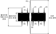
다음으로, 반송파군 생성부(62)에 의해 생성되는 반송파군의 상세한 것에 대하여, 도 3~도 12를 이용해서 설명한다. 도 3은 주파수 영역에 있어서의 반송파군의 파형의 일례를 나타내는 도면이다. 도 4는 시간 영역에 있어서의 반송파군의 파형의 일례를 나타내는 도면이다. 또, 도 3에 있어서, 가로축은 주파수를 나타내고, 세로축은 진폭을 나타낸다. 또, 도 4에 있어서, 가로축은 시간을 나타내고, 세로축은 진폭을 나타낸다. 또, 도 3 및 도 4에 있어서, 진폭은 정규화되어 있는 것으로 한다.Next, details of the carrier wave group generated by the carrier wave
도 3에 나타내는 반송파군은 주파수 영역에 있어서 주파수가 상이한 복수의 반송파(f1~f7)로 이루어진다. 복수의 반송파(f1~f7)의 수(N)는 7이다. 또, 반송파군의 중심 주파수(fc)는 13.56MHz로 설정된다. 또, 복수의 반송파(f1~f7)의 진폭치는 동일하다. 또, 복수의 반송파(f1~f7)의 주파수 간격(Δf)은 10KHz이며, 반송파(f1~f7)의 초기 위상은 서로 이웃하는 반송파에서, 90°씩 어긋나게 설정되어 있다. 이 반송파군의 주파수 대역은 13.56MHz ± 30KHz(대역폭 60KHz)로 된다. 도 3에 나타내는 반송파군의 파형은 시간 영역에 있어서 도 4에 나타내는 파형으로 변환된다. 즉, 도 4에 나타내는 반송파군은 시간 영역에 있어서 제 1 피크 부분(P1)과 제 1 피크 부분(P1)보다 절대치가 작은 제 2 피크 부분(P2)이 교대로 출현하는 진폭 파형(이하 적절히 「진폭 파형」이라고 부른다)에 의해 나타내어진다. 이하에서는, 진폭 파형의 특성으로서, (1) 제 1 피크 부분(P1)과 제 2 피크 부분(P2)의 차(ΔP), (2) 제 1 피크 부분(P1)의 출현 시간(T1)과 제 2 피크 부분(P2)의 출현 시간(T2)의 총 합에 대한 제 1 피크 부분(P1)의 출현 시간(T1)의 비, 및 (3) 서로 이웃하는 2개의 제 1 피크 부분(P1)의 시간 간격(ΔT)을 차례로 설명한다.The carrier group shown in Fig. 3 is composed of a plurality of carriers f1 to f7 having different frequencies in the frequency domain. The number N of the plurality of carriers f1 to f7 is seven. The center frequency fc of the carrier group is set to 13.56 MHz. The amplitude values of the plurality of carriers f1 to f7 are the same. The frequency intervals f of the plurality of carriers f1 to f7 are 10 KHz and the initial phases of the carriers f1 to f7 are set to be shifted by 90 degrees from the adjacent carrier waves. The frequency band of this carrier group is 13.56 MHz ± 30 KHz (bandwidth 60 KHz). The waveform of the carrier wave group shown in Fig. 3 is converted into the waveform shown in Fig. 4 in the time domain. That is, in the carrier wave group shown in Fig. 4, the first peak portion P1 in the time domain and the amplitude waveform (hereinafter referred to as " second peak portion P1 ") in which the second peak portion P2 having an absolute value smaller than that of the first peak portion P1 alternately appear Quot; amplitude waveform "). Hereinafter, the characteristics of the amplitude waveform will be described as characteristics of (1) the difference? P between the first peak portion P1 and the second peak portion P2, (2) the appearance time T1 of the first peak portion P1, (T1) of the first peak portion P1 to the total sum of the appearance times T2 of the second peak portions P2 and (3) the ratio of the two first peak portions P1 adjacent to each other, The time interval?
진폭 파형에 있어서의, 제 1 피크 부분(P1)과 제 2 피크 부분(P2)의 차(ΔP)는 복수의 반송파(f1~f7) 중, 반송파군의 중심 주파수(fc)에 대응하는 반송파의 진폭치와, 반송파군의 중심 주파수(fc)에 응한 반송파 이외의 반송파의 진폭치의 비에 따라서 변동한다.The difference AP between the first peak portion P1 and the second peak portion P2 in the amplitude waveform corresponds to the difference between the carrier frequencies f1 to f7 of the carrier wave corresponding to the center frequency fc of the carrier wave group among the plurality of carrier waves f1 to f7 Varies according to the ratio of the amplitude value and the amplitude value of carrier waves other than the carrier wave corresponding to the center frequency fc of the carrier wave group.
도 5는 반송파군의 중심 주파수(fc)에 대응하는 반송파의 진폭치와, 반송파군의 중심 주파수(fc)에 따른 반송파 이외의 반송파의 진폭치의 비의 설명에 제공하는 도면이다. 도 5에 나타내는 바와 같이, 반송파군의 중심 주파수(fc)에 대응하는 반송파(f4)의 진폭치(Ac)와, 반송파군의 중심 주파수(fc)에 따른 반송파(f4) 이외의 반송파의 진폭치(Ao)의 비(Ao/Ac)는 변경될 수 있다. 비(Ao/Ac)는 예를 들면, 파형 데이터 생성부(71)에 있어서의 파형 데이터의 생성에 이용되는 파라미터가 도시하지 않는 입력 장치에 의해 변경됨으로써 변경된다.5 is a diagram for explaining the ratio of the amplitude value of the carrier wave corresponding to the center frequency fc of the carrier group to the amplitude value of the carrier wave other than the carrier frequency according to the center frequency fc of the carrier group. The amplitude value Ac of the carrier wave f4 corresponding to the center frequency fc of the carrier wave group and the amplitude value Ac of the carrier wave other than the carrier wave f4 corresponding to the center frequency fc of the carrier wave group The ratio (Ao / Ac) of the air-fuel ratio (Ao) can be changed. The ratio Ao / Ac is changed, for example, by changing a parameter used for generating the waveform data in the waveform data generation unit 71 by an input device (not shown).
도 6~도 8은 비(Ao/Ac)에 따른 제 1 피크 부분(P1)과 제 2 피크 부분(P2)의 차(ΔP)의 변동을 나타내는 도면이다. 도 6에서는, 비(Ao/Ac)가 0.05인 경우의 제 1 피크 부분(P1)과 제 2 피크 부분(P2)의 차(ΔP)가 나타나 있다. 도 7에서는, 비(Ao/Ac)가 0.1인 경우의 제 1 피크 부분(P1)과 제 2 피크 부분(P2)의 차(ΔP)가 나타나 있다. 도 8에서는, 비(Ao/Ac)가 0.2인 경우의 제 1 피크 부분(P1)과 제 2 피크 부분(P2)의 차(ΔP)가 나타나 있다. 또, 도 4에서는, 비(Ao/Ac)가 1인 경우의 제 1 피크 부분(P1)과 제 2 피크 부분(P2)의 차(ΔP)가 나타나 있다. 도 4 및 도 6~도 8에 나타내는 바와 같이, 진폭 파형에 있어서의, 제 1 피크 부분(P1)과 제 2 피크 부분(P2)의 차(ΔP)는 비(Ao/Ac)가 증대할수록 증대한다.6 to 8 are diagrams showing the variation of the difference AP between the first peak portion P1 and the second peak portion P2 according to the ratio Ao / Ac. In Fig. 6, the difference? P between the first peak portion P1 and the second peak portion P2 when the ratio Ao / Ac is 0.05 is shown. In Fig. 7, the difference? P between the first peak portion P1 and the second peak portion P2 when the ratio Ao / Ac is 0.1 is shown. 8 shows the difference AP between the first peak portion P1 and the second peak portion P2 when the ratio Ao / Ac is 0.2. 4, the difference? P between the first peak portion P1 and the second peak portion P2 when the ratio Ao / Ac is 1 is shown. As shown in Fig. 4 and Fig. 6 to Fig. 8, the difference AP between the first peak portion P1 and the second peak portion P2 in the amplitude waveform increases as the ratio Ao / Ac increases do.
또, 진폭 파형에 있어서의, 제 1 피크 부분(P1)의 출현 시간(T1)과 제 2 피크 부분(P2)의 출현 시간(T2)의 총 합에 대한 제 1 피크 부분(P1)의 출현 시간(T1)의 비는 복수의 반송파(f1~f7)의 수(N)에 따라 변동한다. 진폭 파형에 있어서의, 제 1 피크 부분(P1)의 출현 시간(T1)과 제 2 피크 부분(P2)의 출현 시간(T2)의 총 합에 대한 제 1 피크 부분(P1)의 출현 시간(T1)의 비를 이하에서는 「 제 1 피크 부분(P1)의 듀티비」라고 부른다. 복수의 반송파(f1~f7)의 수(N)는 예를 들면, 파형 데이터 생성부(71)에 있어서의 파형 데이터의 생성에 이용되는 파라미터가 도시하지 않는 입력 장치에 의해 변경됨으로써 변경된다. The appearance time of the first peak portion P1 with respect to the total sum of the appearance time T1 of the first peak portion P1 and the appearance time T2 of the second peak portion P2 in the amplitude waveform (T1) varies according to the number (N) of the plurality of carriers (f1 to f7). The appearance time T1 of the first peak portion P1 with respect to the total sum of the appearance time T1 of the first peak portion P1 and the appearance time T2 of the second peak portion P2 in the amplitude waveform, ) Is hereinafter referred to as " duty ratio of the first peak portion P1 ". The number N of the plurality of carriers f1 to f7 is changed, for example, by changing a parameter used for generation of waveform data in the waveform data generation unit 71 by an input device (not shown).
도 9 및 도 10은 수(N)에 따른 제 1 피크 부분(P1)의 듀티비의 변동을 나타내는 도면이다. 도 9에서는, 수(N)가 3인 경우의 제 1 피크 부분(P1)의 출현 시간(T1) 및 제 2 피크 부분(P2)의 출현 시간(T2)이 나타나 있다. 도 10에서는, 수(N)가 13인 경우의 제 1 피크 부분(P1)의 출현 시간(T1) 및 제 2 피크 부분(P2)의 출현 시간(T2)이 나타나 있다. 또, 도 4에서는, 수(N)가 7인 경우의 제 1 피크 부분(P1)의 출현 시간(T1) 및 제 2 피크 부분(P2)의 출현 시간(T2)이 나타나 있다. 도 4, 도 9 및 도 10에 나타내는 바와 같이, 진폭 파형에 있어서의 제 1 피크 부분(P1)의 출현 시간(T1)은 수(N)가 증가할수록 감소하고, 진폭 파형에 있어서의 제 2 피크 부분(P2)의 출현 시간(T2)은 수(N)가 증가할수록 증가한다. 즉, 제 1 피크 부분(P1)의 듀티비는 수(N)가 증가할수록 감소한다.Figs. 9 and 10 are diagrams showing the variation of the duty ratio of the first peak portion P1 according to the number (N). 9, the appearance time T1 of the first peak portion P1 and the appearance time T2 of the second peak portion P2 when the number N is 3 are shown. Fig. 10 shows the appearance time T1 of the first peak portion P1 and the appearance time T2 of the second peak portion P2 when the number N is 13. 4, the appearance time T1 of the first peak portion P1 and the appearance time T2 of the second peak portion P2 when the number N is 7 are shown. As shown in Figs. 4, 9 and 10, the appearance time T1 of the first peak portion P1 in the amplitude waveform decreases as the number N increases, and the second peak The appearance time T2 of the portion P2 increases as the number N increases. That is, the duty ratio of the first peak portion P1 decreases as the number N increases.
또, 진폭 파형에 있어서의 서로 이웃하는 2개의 제 1 피크 부분(P1)의 시간 간격(ΔT)은 복수의 반송파(f1~f7)의 주파수 간격(Δf)에 따라서 변동한다. 복수의 반송파(f1~f7)의 주파수 간격(Δf)은 예를 들면, 파형 데이터 생성부(71)에 있어서의 파형 데이터의 생성에 이용되는 파라미터가 도시하지 않는 입력 장치에 의해 변경됨으로써 변경된다.The time interval T of the two first peak portions P1 adjacent to each other in the amplitude waveform varies in accordance with the frequency interval f of the plurality of carriers f1 to f7. The frequency interval? F of the plurality of carriers f1 to f7 is changed by, for example, changing parameters used for generation of waveform data in the waveform data generation unit 71 by an input device (not shown).
도 11 및 도 12는 주파수 간격(Δf)에 따른 서로 이웃하는 2개의 제 1 피크 부분(P1)의 시간 간격(ΔT)의 변동을 나타내는 도면이다. 도 11에서는 주파수 간격(Δf)이 50KHz인 경우의 서로 이웃하는 2개의 제 1 피크 부분(P1)의 시간 간격(ΔT)이 나타나 있다. 도 12에서는 주파수 간격(Δf)이 100KHz인 경우의 서로 이웃하는 2개의 제 1 피크 부분(P1)의 시간 간격(ΔT)이 나타나 있다. 또, 도 4에서는 주파수 간격(Δf)이 10KHz인 경우의 서로 이웃하는 2개의 제 1 피크 부분(P1)의 시간 간격(ΔT)이 나타나 있다. 도 4, 도 11 및 도 12에 나타내는 바와 같이, 진폭 파형에 있어서의 서로 이웃하는 2개의 제 1 피크 부분(P1)의 시간 간격(ΔT)은 복수의 반송파(f1~f7)의 주파수 간격(Δf)이 증가할수록 감소한다.Figs. 11 and 12 are diagrams showing the variation of the time interval? T between two neighboring first peak portions P1 according to the frequency interval? F. In Fig. 11, the time interval T of the two adjacent first peak portions P1 when the frequency interval f is 50 KHz is shown. 12 shows the time interval T of two adjacent first peak portions P1 when the frequency interval f is 100 KHz. In Fig. 4, the time interval? T between two neighboring first peak portions P1 when the frequency interval? F is 10 KHz is shown. As shown in Figs. 4, 11 and 12, the time interval [Delta] T of the two first peak portions P1 adjacent to each other in the amplitude waveform has a frequency interval [Delta] f (f1 to f7) ) Decreases.
도 13은 반송파군에 의한 작용을 설명하기 위한 도면이다. 반송파군 생성부(62)에 의해 생성되는 반송파군의 진폭 파형에서는, 도 13에 나타내는 바와 같이, 제 1 피크 부분(P1)과 제 1 피크 부분(P1)보다 절대치가 작은 제 2 피크 부분(P2)이 교대로 출현한다. 그리고, 제 1 피크 부분(P1)의 출현에 의해, 처리 용기(12) 내에 「플라즈마 착화 피크 전계」가 형성된다. 「플라즈마 착화 피크 전계」는 플라즈마의 생성(착화)에 필요한 방전을 일으키는 전계이다. 처리 용기(12) 내에 「플라즈마 착화 피크 전계」가 형성되면, 방전에 의한 플라즈마의 전리가 가속되어, 플라즈마 밀도가 순간적으로 증가한다. 한편으로, 제 2 피크 부분(P2)의 출현에 의해, 처리 용기(12) 내에 「플라즈마 유지 전계」가 형성된다. 「플라즈마 유지 전계」는 플라즈마의 유지에 필요한 방전을 일으키는 전계를 나타내며, 「플라즈마 착화 피크 전계」보다 절대치가 작다. 처리 용기(12) 내에 「플라즈마 유지 전계」가 형성되면, 방전에 의한 플라즈마의 전리가 억제되어, 플라즈마 밀도의 증가가 억제된다. 반송파군 생성부(62)에 의해 생성되는 반송파군은 처리 용기(12) 내에 「플라즈마 착화 피크 전계」와 「플라즈마 유지 전계」를 교대로 형성시킨다. 이것에 의해, 플라즈마 밀도가 과도하게 증가하는 사태가 회피되고, 또한, 플라즈마의 유지를 위한 충분한 전계가 확보된다.13 is a diagram for explaining an action by a carrier group. 13, in the amplitude waveform of the carrier wave group generated by the carrier wave
다음으로, 제 1 실시 형태에 따른 플라즈마 처리 장치(10)를 이용한 플라즈마 처리 방법에 대해, 도 14를 이용해서 설명한다. 도 14는 제 1 실시 형태에 따른 플라즈마 처리 방법의 흐름도이다.Next, a plasma processing method using the
도 14에 나타내는 바와 같이, 플라즈마 처리 장치(10)의 반송파군 생성부(62)는 반송파군을 생성한다(스텝 S101). 반송파군 생성부(62)에 의해 생성되는 반송파군은 주파수 영역에 있어서 주파수가 상이한 복수의 반송파로 이루어진다. 또, 반송파군 생성부(62)에 의해 생성되는 반송파군은 시간 영역에 있어서 제 1 피크 부분과 제 1 피크 부분보다 절대치가 작은 제 2 피크 부분이 교대로 출현하는 진폭 파형에 의해 나타내어진다.As shown in Fig. 14, the carrier wave
하부 전극(LE)은 반송파군을 이용해서, 처리 용기(12) 내에 플라즈마를 생성한다(스텝 S102).The lower electrode LE generates a plasma in the
처리를 종료할 것인지 결정된다(스텝 S103). 플라즈마 처리 장치(10)는 처리를 계속하는 경우(스텝 S103 부정), 처리를 스텝 S101로 되돌리고, 처리를 종료하는 경우(스텝 S103 긍정), 처리를 종료한다.It is determined whether to end the processing (step S103). When the
제 1 실시 형태에 따른 플라즈마 처리 장치(10)에 의하면, 시간 영역에 있어서 제 1 피크 부분과 제 2 피크 부분이 교대로 출현하는 진폭 파형에 의해 나타내어지는 반송파군을 생성하고, 해당 반송파군을 이용해서 처리 용기(12) 내에 플라즈마를 생성한다. 이 때문에, 처리 용기(12) 내에 「플라즈마 착화 피크 전계」와 「플라즈마 유지 전계」를 교대로 형성시킬 수 있고, 이것에 의해, 플라즈마 밀도가 과도하게 증가하는 사태가 회피되고, 또한, 플라즈마의 유지를 위한 충분한 전계가 확보된다. 결과적으로, 저압 또한 저플라즈마 밀도하에서 플라즈마를 안정적으로 유지할 수 있다. 또한, 이온 에너지의 분포의 제어성을 향상할 수도 있다.According to the
다음으로, 제 1 실시 형태에 따른 플라즈마 처리 장치(10)에 의한 효과(플라즈마의 유지)에 대해, 도 15를 이용해서 설명한다. 도 15는 제 1 실시 형태에 따른 플라즈마 처리 장치에 의한 효과(플라즈마의 유지)의 설명에 제공하는 도면이다. 도 15에 있어서, 가로축은 압력[Torr]를 나타내고, 세로축은 플라즈마 밀도[ions/cm3]를 나타낸다. 또, 도 15에 있어서, 영역(501)은 고주파 전원에 의해 생성되는 고주파 전력을 이용한 종래의 플라즈마 처리 장치를 이용한 경우에, 플라즈마가 유지되는 영역을 나타낸다. 또, 도 15에 있어서, 영역(502)은 제 1 실시 형태에 따른 플라즈마 처리 장치(10)를 이용한 경우에, 플라즈마가 유지되는 영역을 나타낸다.Next, an effect (plasma holding) by the
도 15에 나타내는 바와 같이, 종래의 플라즈마 처리 장치에서는, 압력이 5[mTorr]이상이고, 또한, 플라즈마 밀도가 1E+10[ions/cm3]이상인 환경하에서만 플라즈마가 유지되었다. 이것에 대해, 제 1 실시 형태에 따른 플라즈마 처리 장치(10)에서는, 압력이 5[mTorr]미만이고, 또한, 플라즈마 밀도가 1E+10[ions/cm3]미만인 환경하에서도 플라즈마가 유지되었다. 즉, 제 1 실시 형태에 따른 플라즈마 처리 장치(10)에서는, 종래의 플라즈마 처리 장치와 비교해서, 저압 또한 저플라즈마 밀도하에서 플라즈마를 안정적으로 유지할 수 있었다., In the conventional plasma processing apparatus, as shown in Figure 15, and the pressure is more than 5 [mTorr], In addition, the plasma was maintained only with the plasma density of 1E + 10 [ions / cm 3 ] or more environments. In contrast, in the
다음으로, 제 1 실시 형태에 따른 플라즈마 처리 장치(10)에 의한 효과(이온 에너지의 분포)에 대해, 도 16을 이용해서 설명한다. 도 16은 제 1 실시 형태에 따른 플라즈마 처리 장치에 의한 효과(이온 에너지 분포)의 설명에 제공하는 도면이다. 도 16에 있어서, 가로축은 웨이퍼(W)에 입사하는 이온의 에너지(이하 「이온 에너지」라고 부른다)를 나타내고, 세로축은 웨이퍼(W)에 입사하는 이온의 출현 확률을 나타내고 있다. 또, 도 16에 있어서, 그래프(511)는 고주파 전원에 의해 생성되는 고주파 전력을 이용한 종래의 플라즈마 처리 장치를 이용한 경우의 이온 에너지의 분포를 나타낸다. 또, 도 16에 있어서, 그래프(512)는 제 1 실시 형태에 따른 플라즈마 처리 장치(10)를 이용한 경우의 이온 에너지의 분포를 나타낸다.Next, the effect (ion energy distribution) of the
도 16에 나타내는 바와 같이, 종래의 플라즈마 처리 장치에서는, 이온 에너지의 최소치 및 최대치 부근에서 이온의 출현 확률의 피크가 분산된다. 이것에 대해, 제 1 실시 형태에 따른 플라즈마 처리 장치(10)에서는 특정의 이온 에너지 부근에 이온의 출현 확률의 피크가 집중했다. 즉, 제 1 실시 형태에 따른 플라즈마 처리 장치(10)에서는, 종래의 플라즈마 처리 장치와 비교해서, 이온 에너지의 분포의 제어성을 향상시킬 수 있었다.As shown in Fig. 16, in the conventional plasma processing apparatus, peaks of the appearance probability of ions are dispersed near the minimum value and the maximum value of the ion energy. On the other hand, in the
이상, 제 1 실시 형태에 따른 플라즈마 처리 장치(10)에 의하면, 시간 영역에 있어서 제 1 피크 부분과 제 2 피크 부분이 교대로 출현하는 진폭 파형에 의해 나타내어지는 반송파군을 생성하고, 해당 반송파군을 이용해서 처리 용기(12) 내에 플라즈마를 생성한다. 이 때문에, 처리 용기(12) 내에 「플라즈마 착화 피크 전계」와 「플라즈마 유지 전계」를 교대로 형성시킬 수 있고, 이것에 의해, 플라즈마 밀도가 과도하게 증가하는 사태가 회피되고, 또한, 플라즈마의 유지를 위한 충분한 전계가 확보된다. 결과적으로, 저압 또한 저플라즈마 밀도하에서 플라즈마를 안정적으로 유지할 수 있다. 또한, 이온 에너지의 분포의 제어성을 향상할 수도 있다.As described above, according to the
또, 개시 기술은 상기 실시 형태로 한정되는 것이 아니고, 그 요지의 범위 내에서 여러 변형이 가능하다.It should be noted that the starting technique is not limited to the above-described embodiment, and various modifications are possible within the scope of the present invention.
상기 실시 형태에서는, 파형 데이터 생성부(71)가 1개의 파형 데이터를 생성하고, 변조부(78)가 1개의 파형 데이터에 따라서 반송파군을 생성하는 예를 나타냈지만, 개시 기술은 이것에는 한정되지 않는다. 도 17 및 도 18은 변형예 1의 설명에 제공되는 도면이다. 예를 들면, 파형 데이터 생성부(71)는 도 17에 나타내는 바와 같이, 제 1 시간에 제 1 파형 데이터를 생성하고, 제 1 시간의 다음의 제 2 시간에, 제 1 파형 데이터와는 상이한 제 2 파형 데이터를 생성해도 좋다. 이 경우, 변조부(78)는 도 18에 나타내는 바와 같이, 제 1 시간에 제 1 파형 데이터에 따라 반송파군을 생성하고, 제 2 시간에 제 2 파형 데이터에 따라 반송파군을 생성한다. 도 18의 예에서는, 제 1 파형 데이터에 따라 생성된 반송파군은 시간 영역에 있어서 제 1 피크 부분(P1)과 제 1 피크 부분(P1)보다 절대치가 작은 제 2 피크 부분(P2)이 교대로 출현하는 진폭 파형에 의해 나타내어진다. 이것에 의해, 제 1 시간에서는, 제 1 피크 부분(P1)의 출현에 의해, 처리 용기(12) 내에 「플라즈마 착화 피크 전계」가 형성되고, 제 2 피크 부분(P2)의 출현에 의해, 처리 용기(12) 내에 「플라즈마 유지 전계」가 형성된다. 이것에 대해, 제 2 파형 데이터에 따라 생성된 반송파군은 시간 영역에 있어서 제 3 피크 부분(P3)과 제 3 피크 부분(P3)보다 절대치가 작은 제 4 피크 부분(P4)이 교대로 출현하는 진폭 파형에 의해 나타내어진다. 제 3 피크 부분(P3)은 제 1 피크 부분(P1)보다 절대치가 크다. 이것에 의해, 제 2 시간에서는 제 3 피크 부분(P3)의 출현에 의해, 웨이퍼(W)에 입사하는 이온을 가속시키는 전력인 「이온 가속 전력」이 하부 전극(LE)에 인가된다. In the above embodiment, the waveform data generating unit 71 generates one waveform data, and the modulating unit 78 generates the carrier wave group in accordance with one piece of waveform data. However, the starting technique is not limited to this Do not. 17 and 18 are views provided in the explanation of the first modification. For example, as shown in Fig. 17, the waveform data generation section 71 generates first waveform data at a first time, and generates a second waveform data at a second time following the first time, 2 waveform data may be generated. In this case, as shown in Fig. 18, the modulator 78 generates a carrier wave group according to the first waveform data at a first time, and a carrier wave group according to the second waveform data at a second time. In the example of Fig. 18, the carrier wave group generated according to the first waveform data has the first peak portion P1 in the time domain and the second peak portion P2 having the absolute value smaller than the first peak portion P1 alternately And is represented by an amplitude waveform appearing. Thereby, at the first time, the appearance of the first peak portion P1 forms a "plasma complexing peak electric field" in the
또, 도 19 및 도 20은 변형예 2의 설명에 제공하는 도면이다. 예를 들면, 파형 데이터 생성부(71)는 도 19에 나타내는 바와 같이, 제 1 파형 데이터와 제 1 파형 데이터와는 상이한 제 2 파형 데이터가 합성되어 얻어지는 합성 파형 데이터를 파형 데이터로서 생성해도 좋다. 이 경우, 변조부(78)는 도 20에 나타내는 바와 같이, 제 1 피크 부분(P1)과 제 1 피크 부분(P1)보다 절대치가 작은 제 2 피크 부분(P2)이 교대로 출현하고, 또한, 제 3 피크 부분(P3)이 임의의 시간에 출현하는 반송파군을 합성 파형 데이터에 따라 생성한다. 제 3 피크 부분(P3)은 제 1 피크 부분(P1)보다 절대치가 크다. 도 20의 예에서는, 제 1 피크 부분(P1)의 출현에 의해, 처리 용기(12) 내에 「플라즈마 착화 피크 전계」가 형성되고, 제 2 피크 부분(P2)의 출현에 의해, 처리 용기(12) 내에 「플라즈마 유지 전계」가 형성된다. 또, 제 3 피크 부분(P3)의 출현에 의해, 웨이퍼(W)에 입사하는 이온을 가속시키는 전력인 「이온 가속 전력」이 하부 전극(LE)에 인가된다. 19 and 20 are views provided for explanation of the second modification. For example, as shown in Fig. 19, the waveform data generating unit 71 may generate the composite waveform data obtained by synthesizing the first waveform data and the second waveform data different from the first waveform data, as the waveform data. In this case, as shown in Fig. 20, the modulator 78 alternately shows the first peak portion P1 and the second peak portion P2 having an absolute value smaller than that of the first peak portion P1, And a carrier wave group in which the third peak portion P3 appears at an arbitrary time is generated in accordance with the synthesized waveform data. The third peak portion P3 has an absolute value larger than the first peak portion P1. In the example of Fig. 20, by the appearance of the first peak portion P1, a "plasma ignition peak electric field" is formed in the
또, 상기 실시 형태에서는, 반송파군 생성부(62)에 의해 생성되는 반송파군이 하부 전극(LE)에 공급되는 예를 나타냈지만, 개시 기술은 이것에는 한정되지 않는다. 예를 들면, 반송파군은 상부 전극(30)에 공급되어도 좋다. 상부 전극(30)에 반송파군이 공급되면, 하부 전극(LE)과 상부 전극(30)의 사이의 처리 공간(S)에 전계가 형성된다. 처리 용기(12) 내에 도입된 가스는 처리 공간(S)에 형성된 전계에 의해 플라즈마화되어, 처리 공간(S)에서 플라즈마가 생성된다. 이때, 상부 전극(30)은 반송파군을 이용해서, 처리 용기(12) 내에 플라즈마를 생성하는 플라즈마 생성부로서 기능한다.In the above embodiment, the example in which the carrier wave group generated by the carrier wave
(제 2 실시 형태) (Second Embodiment)
다음으로, 제 2 실시 형태에 대해 설명한다. 도 21은 제 2 실시 형태에 따른 플라즈마 처리 장치를 나타내는 도면이다. 제 2 실시 형태에 따른 플라즈마 처리 장치(10)는 도 1에 나타내는 제 1 실시 형태에 따른 플라즈마 처리 장치(10)와 대략 동일한 구성이기 때문에, 동일한 부분에 대해서는 동일한 부호를 부여해 설명을 생략하고, 주로 상이한 부분에 대해서 설명한다.Next, the second embodiment will be described. 21 is a view showing a plasma processing apparatus according to the second embodiment. Since the
제 2 실시 형태에 따른 플라즈마 처리 장치(10)는 반송파군 생성부(62), 증폭기(64) 및 정합기(66)를 대신해서, 반송파군 생성부(100)와, 방향성 결합기(102)와, 정합기(104)를 갖는다.The
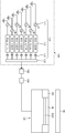
반송파군 생성부(100)는 반송파군을 생성한다. 예를 들면, 반송파군 생성부(100)는 주파수가 상이한 복수의 전기 신호를 합성한 반송파군을 생성한다. 반송파군 생성부(100)에 의해 생성되는 반송파군은 주파수 영역에 있어 주파수가 상이한 복수의 반송파로 이루어진다. 또, 반송파군 생성부(100)에 의해 생성되는 반송파군은 시간 영역에 있어 제 1 피크 부분과, 제 1 피크 부분보다 절대치가 작은 제 2 피크 부분이 교대로 출현하는 진폭 파형에 의해 나타내어진다. 반송파군 생성부(100)에 의해 생성되는 반송파군의 상세한 것에 대해서는, 후술된다.The carrier
도 22는 제 2 실시 형태에 있어서의 반송파군 생성부를 나타내는 도면이다. 반송파군 생성부(100)는 도 22에 나타내는 바와 같이, 각각 반송파의 전기 신호를 생성하는 복수의 생성 회로(110)가 마련되어 있다. 예를 들면, 도 22의 예에서는, 반송파군 생성부(100)는 7개의 생성 회로(110)가 병렬로 마련되어 있다. 또, 생성 회로(110)의 수는 7개로 한정되는 것은 아니다. 반송파군 생성부(100)는 제어부(Cnt)로부터의 제어에 근거해서, 반송파군을 생성한다. 예를 들면, 반송파군 생성부(100)는 제어부(Cnt)로부터 각 생성 회로(110)에서 생성하는 반송파를 지정하는 파라미터(예를 들면, 주파수, 위상, 진폭의 증폭율 등)를 취득하고, 취득한 파라미터를 이용해 반송파군을 생성한다.22 is a diagram showing a carrier group generation unit according to the second embodiment. As shown in FIG. 22, the carrier
생성 회로(110)는 신호 발생기(111)와, 위상 시프터(112)와, 파워 앰프(113)를 각각 갖는다. 신호 발생기(111)는 위상 시프터(112)와 접속되어 있다. 또, 신호 발생기(111)는 접지되어 있다. 신호 발생기(111)는 각각 반송파의 전기 신호를 생성한다. 예를 들면, 신호 발생기(111)는 각각 파라미터로 지정된 주파수의 신호를 생성한다. 신호 발생기(111)는 생성한 전기 신호를 위상 시프터(112)에 출력한다. 위상 시프터(112)는 파워 앰프(113)와 접속되어 있다. 위상 시프터(112)는 입력된 반송파의 전기 신호의 위상을 시프트한다. 예를 들면, 위상 시프터(112)는 입력된 반송파의 전기 신호를, 파라미터로 지정된 것만큼만 위상을 시프트해서 파워 앰프(113)에 출력한다. 파워 앰프(113)는 입력된 반송파의 전기 신호를, 파라미터로 지정된 증폭율로 증폭해서 출력한다.The
반송파군 생성부(100)는 출력 합성기(115)를 가지고 있다. 각 생성 회로(110)의 파워 앰프(113)는 출력 합성기(115)에 접속되어 있다. 출력 합성기(115)에는 각 파워 앰프(113)에서 증폭된 반송파의 전기 신호가 입력된다. 출력 합성기(115)는 각 파워 앰프(113)에서 증폭된 반송파의 전기 신호를 합성해서 반송파군을 생성한다. 출력 합성기(115)는 생성한 반송파군의 전기 신호를 방향성 결합기(102)에 출력한다.The
방향성 결합기(102)는 입력된 반송파군의 전기 신호를 정합기(104)에 출력한다. 또, 방향성 결합기(102)는 도시하지 않는 검출부를 접속해서, 방향성 결합기(102)로부터 정합기(104)에 흐르는 전기 신호의 레벨이나 파형을 검출부에 의해 검출하고, 검출 결과를 제어부(Cnt)에 통지해도 좋다. 제어부(Cnt)는 통지된 검출 결과에 근거해서, 반송파군이 소망의 상태로 되도록, 각 생성 회로(110)에서 생성하는 반송파를 지정하는 파라미터를 제어해도 좋다.The
정합기(104)는 입력된 반송파군의 전기 신호를 하부 전극(LE)에 공급한다. 정합기(104)는 반송파군 생성부(100)측의 출력 임피던스와 부하측(하부 전극(LE)측)의 입력 임피던스를 정합한다. 정합기(104)는 통과하는 반송파군의 주파수 대역에 대응한 광대역 타입의 것으로 하는 것이 바람직하다. 또, 파워 앰프(113)는 진폭이 변화하는 파형을 왜곡하지 않고 증폭하기 위해서 직선성이 높은 증폭기일 필요가 있다. 또, 위상 시프터(112), 방향성 결합기(102) 및 정합기(104)는 본 발명의 주파수 대역에 있어 주파수 특성이 양호한 것과, 위상 왜곡이 적은 것이 바람직하다.The
여기서, 반송파군 생성부(100)에 있어서의 반송파군의 생성 처리의 일례를 설명한다. 반송파군 생성부(100)에서는, 각 생성 회로(110)에서, 소정의 주파수 간격(Δf)으로 주파수가 상이한 반송파를 생성한다. 도 23은 각 생성 회로에서 생성되는 반송파의 주파수의 일례를 나타내는 도면이다. 도 23에서, 가로축은 주파수를 나타내고, 세로축은 진폭을 나타낸다. 진폭은 반송파에 의해 공급되는 전력의 파워를 나타낸다. 도 23에는 중심 주파수(fc)를 13.56MHz로 해서, 주파수 간격(Δf)의 7개의 반송파(f1~f7)의 주파수가 나타내어져 있다. 각 생성 회로(110)는 도 23에 나타내는 각 주파수의 반송파(f1~f7)를 생성한다. 또, 생성하는 반송파의 수(N)는 7로 한정되는 것이 아니고, 생성 회로(110)의 수 이하이고 복수이면 어느 것이어도 좋다. 반송파의 수(N) 및 주파수 간격(Δf)을 변화시킨 것에 의한 반송파군의 변화에 대해서는, 후술한다.Here, an example of the generation process of the carrier wave group in the carrier
각 위상 시프터(112)는 입력된 반송파의 전기 신호의 위상을 시프트한다. 예를 들면, 각 위상 시프터(112)는 입력된 반송파의 전기 신호를, 인접하는 주파수의 반송파의 전기 신호에 대해서, 소정의 주기만큼 차례로 시프트해서 파워 앰프(113)에 출력한다. 소정의 주기는 1 주기분의 위상을 정수로 나눈 주기에 상당하는 위상으로 하는 것이 바람직하다. 본 실시예에서는, 시프트시키는 주기를, 예를 들면, 90°로 한다. 각 위상 시프터(112)는 입력된 반송파의 전기 신호를, 주파수가 작은 쪽에 인접하는 반송파에 대해서 90°위상을 시프트시켜 파워 앰프(113)에 출력한다. 예를 들면, 반송파(f1)의 위상을 0°로 한 경우, 반송파(f2)는 위상을 90°로 시프트시킨다. 반송파(f3)는 위상을 180°로 시프트시킨다. 반송파(f4)는 위상을 270°로 시프트시킨다. 반송파(f5)는 위상을 0°로 시프트시킨다. 반송파(f6)는 위상을 90°로 시프트시킨다. 반송파(f7)는 위상을 0°로 시프트시킨다. 또, 파워 앰프(113)에 의한 증폭에 의해 전기 신호의 위상이 시프트하는 경우, 각 위상 시프터(112)는 파워 앰프(113)에서의 위상의 시프트분을 고려해서, 파워 앰프(113)에서의 증폭 후에, 시프트량이 소정의 주기로 되도록 시프트시켜도 좋다. 예를 들면, 파워 앰프(113)에서의 위상의 시프트량을 보정 정보로서, 미리 제어부(Cnt)의 기억부에 기억해 두고, 제어부(Cnt)가 보정 정보를 이용해서, 파워 앰프(113)에서의 위상의 시프트량을 뺀 것만큼만 위상의 시프트를 각 위상 시프터(112)에 대해서 지정해서, 각 위상 시프터(112)로 파워 앰프(113)에서의 시프트량을 뺀 것만큼만 위상을 시프트시켜도 좋다.Each
출력 합성기(115)는 각 파워 앰프(113)에서 증폭된 반송파의 전기 신호를 합성한다. 도 24는 반송파의 합성의 일례를 나타내는 도면이다. 또, 도 24에서는, 설명의 간략화를 위해, 3개의 반송파(120, 121, 122)를 합성하는 경우를 나타내고 있다. 도 24에서 가로축은 시간을 나타내고, 세로축은 진폭을 나타낸다. 도 24에는, 주파수 간격(Δf)으로 주파수가 상이한 반송파(120, 121, 122)와, 반송파(120, 121, 122)를 합성한 합성파(130)이 나타내어져 있다. 합성파(130)는 반송파(120, 121, 122)의 공진에 의해, 반송파(120, 121, 122)의 진폭의 동일 방향 피크가 겹치는 부분에서 진폭이 커진다. 예를 들면, 합성파(130)는 피크 부분(131)에서 반송파(120, 121, 122)의 진폭보다 진폭이 커진다. 또, 합성파(130)는 반송파(120, 121, 122)의 진폭이 작은 부분이 겹치는 부분이나, 진폭이 상이한 방향으로 겹치는 부분에서, 진폭이 작아진다. 예를 들면, 합성파(130)는 피크 부분(132)에서 반송파(120, 121, 122)의 진폭보다 진폭이 작아진다.The
합성파(130)는 합성하는 반송파의 수(N)가 많아질수록, 최대의 피크가 커진다. 또, 합성파(130)는 주파수 간격(Δf)을 변화시킴으로써, 최대의 피크가 출현하는 주기가 변화한다.As the number N of synthesized waves to be synthesized increases, the maximum peak of the
여기서, 합성하는 반송파에 의한 반송파군의 전기 신호의 파형의 변화를 설명한다. 먼저, 반송파의 수(N)의 변화에 의한 반송파군의 전기 신호의 파형의 변화를 설명한다. 도 25는 반송파의 수(N)마다의 반송파군의 전기 신호의 파형의 일례를 나타내는 도면이다. 도 25의 예는, 중심 주파수(fc)를 13.56MHz로 하고, 주파수 간격(Δf)을 100KHz로 해서, 반송파의 수(N)를 변경한 경우를 나타내고 있다. 도 25의 하부에는, 수(N)를 1(CW), 3, 5, 7, 13으로 하는 경우의 각 반송파(f)의 주파수, 진폭을 나타낸 그래프로 되어 있다. 도 25의 하부의 그래프는, 가로축이 주파수를 나타내고, 세로축이 진폭을 나타낸다. 또, 각 그래프의 하부에는, 각 반송파(f)의 주파수, 위상이 나타내어져 있다. 또, 도 25의 상부에는, 하부에 나타낸 반송파(f)를 합성한 반송파군의 전기 신호의 파형이 나타내어져 있다. 도 25의 상부의 그래프는, 가로축이 시간을 나타내고, 세로축이 진폭을 나타낸다.Here, the change of the waveform of the electric signal of the carrier wave group by the carrier wave to be synthesized will be described. First, the change of the waveform of the electric signal of the carrier group due to the change of the number N of carriers will be described. 25 is a diagram showing an example of a waveform of an electric signal of a carrier group for each number (N) of carriers. The example of Fig. 25 shows a case where the number of carriers (N) is changed with the center frequency fc set at 13.56 MHz and the frequency interval f set at 100 kHz. 25 is a graph showing the frequencies and amplitudes of the carrier waves f when the numbers N are 1 (CW), 3, 5, 7, and 13, respectively. 25, the horizontal axis represents the frequency and the vertical axis represents the amplitude. In the lower part of each graph, the frequency and phase of each carrier wave f are shown. 25 shows the waveform of the electric signal of the carrier wave group synthesized with the carrier wave f shown at the bottom. 25, the horizontal axis represents time and the vertical axis represents amplitude.
수(N)가 1(CW)인 파형은 주파수(fc)의 반송파뿐이기 때문에, 공진이 발생하고 있지 않다. 한편, 수(N)가 3, 5, 7, 13인 파형은, 반송파의 공진에 의해, 시간 영역에 있어 진폭이 큰 피크 부분과, 진폭이 작은 피크 부분이 출현한다. 또, 진폭이 큰 피크가 발생하는 주기는 주파수 간격(Δf)과 동일한 100KHz의 주기로 된다.Since the waveform of the number (N) is 1 (CW) is only the carrier of the frequency fc, no resonance occurs. On the other hand, in the waveforms with numbers N, 3, 5, 7, and 13, peak portions with large amplitude and peak portions with small amplitude appear in the time domain due to the resonance of the carrier wave. The period in which a peak with a large amplitude occurs is a period of 100 KHz which is the same as the frequency interval? F.
다음으로, 주파수 간격(Δf)의 변화에 의한 반송파군의 전기 신호의 파형의 변화를 설명한다. 도 26은 주파수 간격(Δf)마다의 반송파군의 전기 신호의 파형의 일례를 나타내는 도면이다. 도 26의 예는 중심 주파수(fc)를 13.56MHz로 하고, 반송파(f)를 7개(f1~f7)로 해서, 반송파(f1~f7)의 주파수 간격(Δf)을 변경한 경우를 나타내고 있다. 도 26의 하부에는, 반송파(f1~f7)의 주파수 간격(Δf)을 50KHz, 100KHz, 500KHz로 하는 경우의 반송파(f1~f7)의 주파수, 진폭을 나타낸 그래프로 되어 있다. 도 26의 하부의 그래프는, 가로축이 주파수를 나타내고, 세로축이 진폭을 나타낸다. 또, 각 그래프의 하부에는, 각 반송파(f)의 주파수, 위상이 나타내어져 있다. 또, CW에는, 중심 주파수(fc)를 13.56MHz로 하는 반송파의 진폭이 나타내어져 있다. 또, 도 26의 상부에는, 하부에 나타낸 반송파(f1~f7)를 합성한 반송파군의 전기 신호의 파형이 나타내어져 있다. 도 26의 상부의 그래프는, 가로축이 시간을 나타내고, 세로축이 진폭을 나타낸다.Next, the change of the waveform of the electric signal of the carrier wave group due to the change of the frequency interval f will be described. 26 is a diagram showing an example of a waveform of an electric signal of a carrier group for each frequency interval f. 26 shows a case in which the frequency interval f of the carrier waves f1 to f7 is changed with the center frequency fc of 13.56 MHz and the carrier frequency f of seven frequencies f1 to f7 . 26 is a graph showing the frequencies and amplitudes of the carrier waves f1 to f7 when the frequency spacing f of the carrier waves f1 to f7 is 50 KHz, 100 KHz, and 500 KHz, respectively. 26, the horizontal axis represents the frequency and the vertical axis represents the amplitude. In the lower part of each graph, the frequency and phase of each carrier wave f are shown. In CW, the amplitude of the carrier wave with the center frequency fc of 13.56 MHz is shown. 26 shows the waveforms of the electric signals of the carrier wave group synthesized with the carrier waves f1 to f7 shown at the bottom. In the upper graph of Fig. 26, the abscissa represents time and the ordinate represents amplitude.
CW의 파형은 주파수(fc)의 반송파뿐이기 때문에, 공진이 발생하고 있지 않다. 한편, 주파수 간격(Δf)을 50KHz, 100KHz, 500KHz으로 하는 파형은, 반송파의 공진에 의해, 시간 영역에 있어 진폭이 큰 피크 부분과, 진폭이 작은 피크 부분이 출현한다. 또, 진폭이 큰 피크가 발생하는 주기는 주파수 간격(Δf)과 동일한 주기로 된다.Since the waveform of CW is only a carrier of frequency fc, no resonance occurs. On the other hand, in the waveform having the frequency interval? F of 50 KHz, 100 KHz, and 500 KHz, a peak portion having a large amplitude and a peak portion having a small amplitude appear in the time domain due to the resonance of a carrier wave. The period in which a peak with a large amplitude occurs is the same as the frequency interval? F.
다음으로, 반송파의 진폭의 변화에 의한 반송파군의 전기 신호의 파형의 변화를 설명한다. 도 27은 반송파의 진폭을 변화시켰을 경우의 반송파군의 전기 신호의 파형의 일례를 나타내는 도면이다. 도 27의 예는, 중심 주파수(fc)를 13.56MHz로 하고, 주파수 간격(Δf)을 100KHz로 하고, 반송파를 7개의 f1~f7로 하고, 중심 주파수(fc)로 되는 반송파(f4)의 진폭에 대해서, 반송파(f1~f3, f5~f7)의 진폭을 변화시킨 경우를 나타내고 있다. 도 27의 상부의 그래프는, 가로축이 주파수를 나타내고, 세로축이 진폭을 나타낸다. 도 27의 하부에는, 반송파(f4)의 진폭에 대한 반송파(f1~f3, f5~f7)의 진폭을 X=0, 0.2(20%), 0.5(50%), 0.8(80%), 1(100%)로 해서, 반송파(f1~f7)를 합성한 반송파군의 전기 신호의 파형이 나타내어져 있다. 도 27의 하부의 그래프는, 가로축이 시간을 나타내고, 세로축이 진폭을 나타낸다.Next, the change of the waveform of the electric signal of the carrier wave group due to the change of the amplitude of the carrier wave will be described. 27 is a diagram showing an example of a waveform of an electric signal of a carrier wave group when the amplitude of the carrier wave is changed. 27, the amplitude of the carrier f4, which has the center frequency fc of 13.56 MHz, the frequency interval f of 100 KHz, the carrier frequency of 7 f1 to f7, and the center frequency fc, , The amplitude of the carrier waves f1 to f3 and f5 to f7 is changed. 27, the horizontal axis represents the frequency and the vertical axis represents the amplitude. 27, the amplitudes of the carrier waves f1 to f3 and f5 to f7 with respect to the amplitude of the carrier wave f4 are represented by X = 0, 0.2 (20%), 0.5 (50% (100%), and the waveforms of the electric signals of the carrier wave group synthesized with the carrier waves f1 to f7 are shown. In the graph in the lower part of FIG. 27, the horizontal axis represents time and the vertical axis represents amplitude.
X=0(CW)의 파형은 주파수(fc)의 반송파뿐이기 때문에, 공진이 발생하고 있지 않다. 한편, X=0.2, 0.5, 0.8의 파형은, 반송파의 공진에 의해, 시간 영역에 있어 진폭이 큰 피크 부분과, 진폭이 작은 피크 부분이 출현한다. 또, X가 클수록, 진폭이 큰 피크 부분과, 진폭이 작은 피크 부분의 진폭의 차가 커진다. 또, X=1의 파형은, 반송파(f1~f7)가 동일한 진폭으로 되기 때문에, 도 26의 N=7과 동일한 파형으로 되어 있다.Since the waveform of X = 0 (CW) is only the carrier of frequency fc, no resonance occurs. On the other hand, in the waveforms of X = 0.2, 0.5, and 0.8, a peak portion with large amplitude and a peak portion with small amplitude appear in the time domain due to the resonance of the carrier wave. Further, the larger the value of X, the larger the difference between the amplitudes of the peak portion having a larger amplitude and the peak portion having a smaller amplitude. The waveform of X = 1 has the same waveform as that of N = 7 in Fig. 26 because the carrier waves f1 to f7 have the same amplitude.
이와 같이, 반송파군의 전기 신호의 파형은 합성하는 반송파에 따라서 변화한다. 제어부(Cnt)는 반송파군 생성부(100)에 설정하는 반송파를 지정하는 파라미터를 제어해서, 반송파군 생성부(100)에서 반송파를 생성하는 생성 회로(110)의 수(N)나, 각 생성 회로(110)에서 생성하는 반송파의 주파수, 위상 시프터(112)에서의 위상의 시프트량, 파워 앰프(113)에서의 반송파의 증폭율을 변경함으로써, 반송파군의 파형을 변경할 수 있다. 도 28a~도 28d는 반송파의 지정의 일례를 나타내는 도면이다. 또, 도 28a~도 28d에는, 반송파군 생성부(100)에 13개의 생성 회로(110)가 병렬로 있는 경우의 각 생성 회로(110)에서 생성하는 반송파(f1~f13)의 조건이 나타내어져 있다. 도 28a는 중심 주파수(fc)를 13.56MHz로 하고, 수(N)를 13으로 하고, 주파수 간격(Δf)을 100KHz로 하는 경우의 반송파(f1~f13)의 조건을 나타내고 있다. 도 28b는 중심 주파수(fc)를 13.56MHz로 하고, 수(N)를 7로 하고, 주파수 간격(Δf)을 10KHz로 하는 경우의 반송파(f1~f13)의 조건을 나타내고 있다. 도 28c는 중심 주파수(fc)를 13.56MHz로 하고, 수(N)를 13으로 하고, 주파수 간격(Δf)을 10KHz로 하는 경우의 반송파(f1~f13)의 조건을 나타내고 있다. 도 28d는 중심 주파수(fc)를 13.56MHz로 하고, 수(N)를 10으로 하고, 주파수 간격(Δf)을 10KHz로 하는 경우의 반송파(f1~f13)의 조건을 나타내고 있다. 「ON/OFF」는 반송파를 생성하는 생성 회로(110)를, 반송파를 생성하는 온 상태로 하는지, 반송파를 생성하지 않는 오프 상태로 하는지를 나타내고 있다. 「주파수[MHz]」는 생성하는 반송파의 주파수를 나타내고 있다. 「초기 위상[°]」은 반송파를 시프트시키는 위상을 나타내고 있다. 「상대 전력」은 반송파의 상대 전력을 나타내고 있다. 반송파는 상대 전력이 클수록 증폭되어, 진폭이 커진다.Thus, the waveform of the electric signal of the carrier wave group changes in accordance with the carrier wave to be synthesized. The control unit Cnt controls the parameter designating the carrier wave to be set in the carrier
반송파군 생성부(100)는 제어부(Cnt)로부터 설정된 파라미터에 따라서 생성한 복수의 반송파의 전기 신호를 합성해서 공진시킴으로써, 시간 영역에 있어 제 1 피크 부분과 제 1 피크 부분보다 절대치가 작은 제 2 피크 부분이 교대로 출현하는 진폭 파형에 의해 나타내어지는 반송파군을 생성한다.The carrier
이와 같이 구성된 플라즈마 처리 장치(10)에서는, 상부 전극(30)의 전극판(34)의 가스 토출 구멍(34a)으로부터 처리 용기(12) 내로 가스가 도입된다. 또, 반송파군 생성부(100)에 의해 생성되는 반송파군이 방향성 결합기(102) 및 정합기(104)를 통해서 하부 전극(LE)에 공급된다. 하부 전극(LE)에 반송파군이 공급되면, 하부 전극(LE)과 상부 전극(30)의 사이의 처리 공간(S)에 전계가 형성된다. 처리 용기(12) 내에 도입된 가스는 처리 공간(S)에 형성된 전계에 의해 플라즈마화되고, 처리 공간(S)에서 플라즈마가 생성된다. 이때, 하부 전극(LE)은 반송파군을 이용해서, 처리 용기(12) 내에 플라즈마를 생성하는 플라즈마 생성부로서 기능한다.The gas is introduced into the
이와 같이, 제 2 실시 형태에 따른 플라즈마 처리 장치(10)는 시간 영역에 있어 제 1 피크 부분과 제 2 피크 부분이 교대로 출현하는 진폭 파형에 의해 나타내어지는 반송파군을 생성하고, 상기 반송파군을 이용해서 처리 용기(12) 내에 플라즈마를 생성한다. 이 때문에, 처리 용기(12) 내에 「플라즈마 착화 피크 전계」와 「플라즈마 유지 전계」를 교대로 형성시킬 수 있고, 이것에 의해, 플라즈마 밀도가 과도하게 증가하는 사태가 회피되고, 또한, 플라즈마의 유지를 위한 충분한 전계가 확보된다. 결과적으로, 저압이고 저플라즈마 밀도 하에서 플라즈마를 안정적으로 유지할 수 있다. 또한, 이온 에너지의 분포의 제어성을 향상시킬 수도 있다.As described above, the
또, 제 2 실시 형태에 따른 반송파군 생성부(100)는 소정의 주파수 간격으로 주파수가 상이한 반송파를 생성하고, 생성된 주파수가 상이한 반송파의 위상을 각각 소정의 주기만큼 차례로 시프트하고, 위상이 시프트된 주파수가 상이한 반송파를 합성하여, 반송파군을 생성한다. 이것에 의해, 반송파군 생성부(100)는 제 1 피크 부분 및 제 2 피크 부분의 진폭이나, 제 1 피크 부분과 제 2 피크 부분의 간격, 제 1 피크 부분과 그 다음의 제 1 피크 부분의 간격을 변화시킨 다양한 파형을 생성할 수 있다.The carrier
그런데, 최근, 웨이퍼(W) 등의 기판의 플라즈마 에칭에서는, 미세화에 따라, 개구의 폭에 대해서 에칭을 행하는 깊이가 깊은 고 어스펙트비의 가공이 요구되고 있다. 이러한 고 어스펙트비의 플라즈마 에칭을 행하는 경우, 플라즈마 처리 장치에서는, 고 어스펙트비의 콘택트 홀의 바닥에 이온을 도달시킬 필요가 있다. 플라즈마 처리 장치에서는, 예를 들면, 전원으로부터 하부 전극(LE)에, 도 29에 나타내는 바와 같은 진폭이 일정한 고주파의 전력을 연속으로 공급해서 플라즈마 에칭을 행하는 경우, 콘택트 홀의 바닥에 이온을 도달시키기 위해서, 하부 전극(LE)에 공급하는 전력 P0를 높게 하면, 다음과 같은 문제가 발생하는 경우가 있다. 또, 도 29는 하부 전극에 공급하는 전력의 일례를 나타내는 도면이다.Recently, in the plasma etching of a substrate such as a wafer W, processing of a high aspect ratio in which etching is performed with respect to the width of the opening is required in accordance with miniaturization. When plasma etching is performed at such a high aspect ratio, it is necessary to reach the bottom of the contact hole having a high aspect ratio in the plasma processing apparatus. In the plasma processing apparatus, for example, when plasma etching is performed by continuously supplying a high frequency power having a constant amplitude as shown in Fig. 29 to a lower electrode LE from a power source, in order to reach ions at the bottom of the contact hole And the power P 0 supplied to the lower electrode LE is increased, the following problems may occur. 29 is a diagram showing an example of power supplied to the lower electrode.
도 30은 고 어스펙트비의 플라즈마 에칭을 행하는 경우에 발생하는 문제의 일례를 나타내는 도면이다. 고 어스펙트비의 플라즈마 에칭에서는, 하부 전극(LE)에 공급하는 전압을 높게 하면, 이온이 보다 가속되기 때문에, 마스크의 후퇴가 발생하는 경우가 있다. 또, 고 어스펙트비의 콘택트 홀은 배기 특성이 악화된다. 이 때문에, 콘택트 홀의 하부에서 생긴 반응 생성물이 재부착하거나, 반응 생성물이 배기되었다고 해도 플라즈마에 의해 분해되어 재부착하는 것 등에 의해, 콘택트 홀에 클로깅(clogging), 넥킹(necking)이 발생하는 경우가 있다. 또, 콘택트 홀의 바닥에는, 방향성을 가진 이온밖에 도달하지 않기 때문에, 이온의 전하에 의해 대전하는 경우가 있다. 이 때문에, 대전에 의해 이온이 만곡해서, 콘택트 홀에서 트위스팅(twisting)이 발생하는 경우가 있다.30 is a diagram showing an example of a problem that arises when plasma etching with a high aspect ratio is performed. In the plasma etching of the high aspect ratio, if the voltage supplied to the lower electrode LE is made higher, ions are accelerated more, so that the mask may retreat. In addition, the contact hole of the high aspect ratio deteriorates the exhaust characteristics. For this reason, even if the reaction product formed in the lower portion of the contact hole is reattached or the reaction product is exhausted, clogging or necking occurs in the contact hole due to decomposition and reattachment by plasma . Since ions having only directivity reach only the bottom of the contact hole, they may be charged by the charge of ions. For this reason, ions are curved due to charging, and twisting may occur in the contact holes.
이러한 문제는 전원으로부터 하부 전극(LE)에 전력을 펄스 형상으로 공급함으로써 개선된다. 예를 들면, 도 31에 나타내는 바와 같이, 하부 전극(LE)에 진폭이 일정한 고주파의 전력 PA를 펄스 형상으로 공급해서 플라즈마 에칭을 행하는 것으로 한다. 또, 도 31은 하부 전극에 공급하는 전압의 일례를 나타내는 도면이다. 이 개선된 메카니즘은 다음과 같이 생각된다. 전력 PA가 공급되는 기간 ton에는 고속의 이온이 콘택트 홀의 바닥에 도달한다. 한편, 전력 PA가 공급되지 않는 기간 tOFF에는 플라즈마가 얇게 되고, 반응 생성물의 플라즈마에 의한 분해가 일어날 가능성이 낮고, 반응 생성물에 의해 콘택트 홀의 측벽에 퇴적물이 퇴적하거나 콘택트 홀을 막을 가능성이 낮아진다. 또, 기간 tOFF에는 이온의 전하에 의해 대전이 완화되기 때문에, 이온이 만곡하기 어려워진다. 이것에 의해, 도 32에 나타내는 바와 같이, 고 어스펙트비의 콘택트 홀의 플라즈마 에칭을 행할 수 있다. 또, 도 32는 플라즈마 에칭된 고 어스펙트비의 콘택트 홀의 일례를 나타내는 도면이다.This problem is improved by supplying the power from the power source to the lower electrode LE in a pulse shape. For example, as shown in Fig. 31, a high-frequency power P A having a constant amplitude is supplied in pulse form to the lower electrode LE to perform plasma etching. 31 is a diagram showing an example of a voltage supplied to the lower electrode. This improved mechanism is thought to be as follows. High-speed ions reach the bottom of the contact hole during the period t on when the power P A is supplied. On the other hand, in a period t OFF in which power P A is not supplied, the plasma is thin, the possibility of decomposition of the reaction product by plasma is low, and the possibility of accumulation of deposits on the sidewall of the contact hole by the reaction product or clogging of the contact hole is low . In addition, in the period t OFF , since the charge is relaxed by the charge of the ions, the ions are less likely to bend. As a result, as shown in Fig. 32, plasma etching of contact holes having a high aspect ratio can be performed. 32 is a view showing an example of a contact hole of the plasma etched high aspect ratio.
그런데, 기간 tOFF에는 하부 전극(LE)에 전력이 공급되지 않기 때문에, 에칭이 행해지지 않는다. 이 때문에, 플라즈마 처리 장치에서는, 하부 전극(LE)에 전력을 펄스 형상으로 공급하는 경우, 듀티비를 내리면, 에칭 레이트가 저하한다. 예를 들면, 하부 전극(LE)에 공급하는 전력의 듀티비를 10%로 하면, 90%의 시간은 하부 전극(LE)에의 전력을 OFF로 하고 있는 것과 같게 된다. 따라서, 듀티비를 10%로 하면, 플라즈마 에칭에 작용하는 실효적인 전력은 1/10로 되어 버린다. 이 때문에, 에칭 레이트가 저하한다. 하부 전극(LE)에 전력을 연속으로 공급했을 경우와 동일한 정도의 에칭 레이트를 얻으려면, 실효적인 전력을 동일하게 할 필요가 있다. 예를 들면, 듀티비를 10%로 하는 경우, 실효적인 전력을 동일하게 하려면, 10배의 전력을 공급할 수 있는 전원이 필요하다. 도 33a는 듀티비와 에칭 레이트의 관계를 설명하는 도면이다. 도 33a에서 가로축은 듀티비를 나타내고, 세로축은 에칭 레이트를 나타낸다. 도 33b는 듀티비와 전원의 용량의 관계를 설명하는 도면이다. 도 33b에 있어서, 가로축은 듀티비를 나타내고, 세로축은 전원의 용량을 나타낸다. 도 33a 및 도 33b에 나타내는 가로축의 듀티비는 우측으로 갈수록 듀티비가 작아지는 것으로 한다. 도 33a의 파선(140)으로 나타내는 바와 같이, 듀티비를 내리면, 에칭 레이트가 저하한다. 그래서, 도 33b의 실선(141)으로 나타내는 바와 같이, 듀티비의 저하에 대응시켜 전원의 용량을 증가시켜 실효적인 전력을 일정하게 유지하는 경우, 도 33a의 실선(142)으로 나타내는 바와 같이, 에칭 레이트를 유지할 수 있다.Incidentally, no power is supplied to the lower electrode LE during the period t OFF , so that etching is not performed. For this reason, in the plasma processing apparatus, when power is supplied to the lower electrode LE in a pulse shape, the etching rate decreases when the duty ratio is lowered. For example, assuming that the duty ratio of the electric power supplied to the lower electrode LE is 10%, the time of 90% becomes equal to turning OFF the electric power to the lower electrode LE. Therefore, when the duty ratio is set to 10%, the effective power for plasma etching becomes 1/10. Therefore, the etching rate decreases. In order to obtain the same etching rate as when the power is continuously supplied to the lower electrode LE, it is necessary to make the effective power the same. For example, when the duty ratio is set to 10%, a power supply capable of supplying 10 times the power is required in order to make the effective power the same. FIG. 33A is a view for explaining the relationship between the duty ratio and the etching rate. FIG. In Fig. 33A, the horizontal axis represents the duty ratio, and the vertical axis represents the etching rate. FIG. 33B is a diagram for explaining the relationship between the duty ratio and the capacity of the power source. FIG. In Fig. 33B, the horizontal axis represents the duty ratio, and the vertical axis represents the capacity of the power source. It is assumed that the duty ratio of the horizontal axis shown in Figs. 33A and 33B becomes smaller toward the right side. As indicated by the
플라즈마 처리 장치는 전원으로부터 하부 전극(LE)에 전력을 펄스 형상으로 공급함으로써, 고 어스펙트비의 콘택트 홀을 에칭할 때의 문제를 개선할 수 있다. 그러나, 플라즈마 처리 장치는 전원으로부터 하부 전극(LE)에 전력을 펄스 형상으로 공급하는 경우, 용량이 큰 전원이 필요하다. 예를 들면, 플라즈마 처리 장치는 1KW의 용량의 전원으로부터 하부 전극(LE)에 전력을 연속으로 공급하는 경우와 동일한 실효적인 전력을, 듀티비를 10%로 한 펄스 형상의 전력으로 실현되게 하는 경우, 10KW의 용량의 전원이 필요하다. 또, 플라즈마 처리 장치는 예를 들면, 10KW의 용량의 전원을 사용한 경우에서도, 듀티비를 5%로 하는 경우, 실효적인 전력이 500 W로 되어 버린다. 전원은 용량이 클수록 비용이 비약적으로 높아지고, 사이즈도 커진다.The plasma processing apparatus can improve the problem of etching a contact hole having a high aspect ratio by supplying power from the power source to the lower electrode LE in a pulse shape. However, when the plasma processing apparatus supplies power in a pulse shape from the power source to the lower electrode LE, a large capacity power source is required. For example, in the case where the plasma processing apparatus realizes the same effective power as the case of continuously supplying power from the power source having the capacity of 1 KW to the lower electrode LE with the pulse-shaped power having the duty ratio of 10% , A power supply of 10KW is required. Further, even when a power source having a capacity of 10 KW is used, for example, when the duty ratio is set to 5%, the effective power becomes 500 W in the plasma processing apparatus. The larger the capacity of the power source, the higher the cost and the larger the size.
한편, 상술한 제 1 실시 형태의 반송파군 생성부(62) 및 제 2 실시 형태의 반송파군 생성부(100)는 시간 영역에 있어 제 1 피크 부분과 제 1 피크 부분보다 절대치가 작은 제 2 피크 부분이 교대로 출현하는 진폭 파형에 의해 나타내어지는 반송파군을 생성할 수 있기 때문에, 상술한 바와 같은 펄스 형상의 파형과 마찬가지로 기능하는 파형을 생성할 수 있다. 특히, 제 2 실시 형태의 반송파군 생성부(100)는 반송파를 생성하는 생성 회로(110)의 수(N)나, 각 생성 회로(110)에서 생성하는 반송파의 주파수, 위상 시프터(112)에서의 위상의 시프트량, 파워 앰프(113)에서의 반송파의 증폭율을 변경함으로써, 펄스 형상의 파형에 가까운 파형을 생성할 수 있다. 또, 상술한 제 1 실시 형태의 반송파군 생성부(62) 및 제 2 실시 형태의 반송파군 생성부(100)는 복수의 반송파를 합성함으로써, 각각의 반송파를 생성하는 각 생성 회로(110)의 전원의 용량을 크게 하지 않아도, 진폭이 큰 반송파군을 생성할 수 있다.On the other hand, in the carrier wave
도 34는 하부 전극에 공급하는 전압의 일례를 나타내는 도면이다. 도 34의 상부에는, 하부 전극(LE)에 고주파의 전력을 연속으로 공급하는 경우(듀티비=100%)와, 듀티비를 50%, 30%, 10%로 해서 펄스 형상으로 고주파의 전력을 공급하는 경우에 하부 전극(LE)에 공급되는 전기 신호의 파형이 나타내어져 있다. 또, 듀티비 50%, 30%, 10%에서는, 각각 전력의 용량을 크게 하고 있어, 진폭이 커지고 있다. 또, 도 34의 하부에는, 중심 주파수(fc)를 13.56MHz로 하고, 주파수 간격(Δf)을 100KHz로 하고, 반송파의 수(N)를 1(CW), 3, 5, 7, 13으로 한 경우에, 하부 전극(LE)에 공급되는 반송파군의 전기 신호의 파형이 나타내어져 있다. 도 34의 각 그래프는, 가로축이 시간을 나타내고, 세로축이 진폭을 나타낸다. 수(N)=3의 파형은 듀티비가 50%인 펄스 형상의 파형과 마찬가지로 기능한다. 수(N)=5의 파형은 듀티비가 30%인 펄스 형상의 파형과 마찬가지로 기능한다. 수(N)=13의 파형은 듀티비가 10%인 펄스 형상의 파형과 마찬가지로 기능한다.34 is a diagram showing an example of a voltage supplied to the lower electrode. In the upper part of FIG. 34, high-frequency power is supplied in the form of pulses at a duty ratio of 50%, 30%, and 10% when the high-frequency power is continuously supplied to the lower electrode LE The waveform of the electric signal supplied to the lower electrode LE is shown. In addition, at the duty ratios of 50%, 30%, and 10%, the power capacity is increased and the amplitude is increased. 34, the center frequency fc is set to 13.56 MHz, the frequency interval f is set to 100 KHz, and the number of carrier waves N is set to 1 (CW), 3, 5, 7, and 13 The waveform of the electric signal of the carrier wave group supplied to the lower electrode LE is shown. In each graph of Fig. 34, the horizontal axis represents time and the vertical axis represents amplitude. The waveform of the number (N) = 3 functions in the same manner as the pulse waveform having the duty ratio of 50%. The waveform of the number (N) = 5 functions in the same manner as the pulse waveform having the duty ratio of 30%. The waveform of the number (N) = 13 functions in the same manner as the pulse waveform having the duty ratio of 10%.
다음으로, 제 2 실시 형태의 반송파군 생성부(100)의 반송파군을 이용해서 플라즈마 에칭을 실시한 경우의 결과의 일례를 설명한다. 도 35는 에칭 레이트의 비교 결과의 일례를 나타내는 도면이다. 도 35의 예는, SiO2의 웨이퍼(W)에 대해서 플라즈마 에칭을 실시한 경우의 에칭 레이트를 나타내고 있다. 도 35에 있어서, 가로축은 주파수 간격(Δf)을 나타내고, 세로축은 에칭 레이트를 나타낸다. 도 35에는, 중심 주파수(fc)를 13.56MHz로 하고, 반송파의 수(N)를 7로 하고, 주파수 간격(Δf)을 변화시켜, 각각 플라즈마 에칭을 행한 경우의 에칭 레이트가 선(150)에 의해 나타내어져 있다. 또, 도 35에는, 듀티비가 30%인 펄스 형상의 파형에 있어서 기간 ton의 출현 주기를 주파수 간격(Δf)에 대응하는 주기로 해서, 각각 플라즈마 에칭을 실시한 경우의 에칭 레이트가 파선(151)에 의해 나타내어져 있다. 도 35에 나타내는 바와 같이, 제 2 실시 형태의 반송파군 생성부(100)는 펄스 형상의 파형과 동일한 에칭 레이트를 얻을 수 있다.Next, an example of a result obtained when plasma etching is performed using the carrier wave group of the carrier wave
이와 같이, 제 2 실시 형태에 따른 반송파군 생성부(100)는 소정의 주파수 간격으로 주파수가 상이한 반송파를 생성하고, 생성된 주파수가 상이한 반송파의 위상을 각각 소정의 주기만큼 차례로 시프트하고, 위상이 시프트된 주파수가 상이한 반송파를 합성하여, 반송파군을 생성한다. 이것에 의해, 반송파군 생성부(100)는 용량이 큰 전원을 사용하지 않아도, 반송파를 합성함으로써, 용량이 큰 전원을 이용한 펄스 형상의 파형과 마찬가지로 기능하는 반송파군의 전기 신호를 생성할 수 있다. 또, 반송파군 생성부(100)는 용량이 큰 전원을 사용하지 않아도 되기 때문에, 전원의 비용을 절약할 수 있고, 전원의 사이즈도 소형화할 수 있다.As described above, the carrier
또, 상기 실시 형태에서는, 제어부(Cnt)로부터 파라미터의 제어에 따라서, 각 신호 발생기(111)가 생성하는 반송파의 주파수와, 각 위상 시프터(112)에 의한 위상의 시프트량과, 각 파워 앰프(113)에 의한 반송파의 증폭율을 변경할 수 있는 경우를 예로 설명했지만, 이것으로 한정되는 것은 아니다. 각 신호 발생기(111)가 생성하는 반송파의 주파수, 각 위상 시프터(112)에 의한 위상의 시프트량 및 각 파워 앰프(113)에 의한 반송파의 증폭율은 각각 고정으로 정해져 있어도 좋다. 예를 들면, 각 신호 발생기(111)는 중심 주파수(fc)를 13.56MHz로 하고, 각각 소정의 주파수 간격(Δf)(예를 들면, 주파수 간격(Δf))으로 반송파(f)의 전기 신호를 고정으로 생성하는 것으로 해도 좋다. 또, 각 위상 시프터(112)는 각각 주파수가 작은 쪽에 인접하는 반송파에 대해서 고정으로 90°위상을 시프트하는 것으로 해도 좋다. 또, 각 파워 앰프(113)는 각각 소정의 증폭율로 반송파를 증폭하는 것으로 해도 좋다.In the above-described embodiment, the frequency of the carrier wave generated by each
또, 상기 실시 형태에서는, 반송파군 생성부(100)에서 생성하는 반송파(f)의 수를 홀수로 한 경우를 예로 설명했지만, 이것으로 한정되는 것은 아니다. 반송파(f)의 수는 짝수이어도 좋다. 이 경우, 예를 들면, 중심 주파수에 대해서 주파수가 대칭으로 되도록 반송파(f)를 생성한다. 예를 들면, 중심 주파수(fc)를 13.56MHz로 하고, 주파수 간격(Δf)을 100KHz로 해서 4개의 반송파(f1~f4)를 생성하는 경우, 반송파(f1)의 주파수는 13.41MHz로 한다. 반송파(f2)의 주파수는 13.51MHz로 한다. 반송파(f3)의 주파수는 13.61MHz로 한다. 반송파(f4)의 주파수는 13.71MHz로 한다.In the above-described embodiment, the number of carrier waves f generated by the carrier
10 : 플라즈마 처리 장치
12 : 처리 용기
30 : 상부 전극
62 : 반송파군 생성부
71 : 파형 데이터 생성부
72 : 양자화부
73 : 역푸리에 변환부
78 : 변조부
100 : 반송파군 생성부
102 : 방향성 결합기
104 : 정합기
110 : 생성 회로
111 : 신호 발생기
112 : 위상 시프터
113 : 파워 앰프
115 : 출력 합성기
LE : 하부 전극
Cnt : 제어부10: plasma processing apparatus 12: processing vessel
30: upper electrode 62: carrier wave group generating unit
71: waveform data generation unit 72: quantization unit
73: Inverse Fourier transform unit 78: Modulation unit
100: carrier group generation unit 102: directional coupler
104: matching circuit 110: generating circuit
111: Signal generator 112: Phase shifter
113: Power amplifier 115: Output synthesizer
LE: lower electrode Cnt: control unit
Claims (11)
주파수 영역에 있어서 주파수가 상이한 복수의 반송파로 이루어지는 반송파군으로서, 시간 영역에 있어서 제 1 피크 부분과 상기 제 1 피크 부분보다 절대치가 작은 제 2 피크 부분이 교대로 출현하는 진폭 파형에 의해 나타내어지는 상기 반송파군을 생성하는 반송파군 생성부와,
상기 반송파군을 이용해서, 상기 처리 용기 내에 플라즈마를 생성하는 플라즈마 생성부
를 갖는 것을 특징으로 하는 플라즈마 처리 장치.
A processing vessel,
A carrier wave group comprising a plurality of carriers having different frequencies in a frequency domain, the carrier wave group having a first peak portion in a time domain and a second peak portion having an absolute value smaller than the first peak portion, A carrier group generating unit for generating a carrier group,
A plasma generator for generating plasma in the processing container by using the carrier group;
And a plasma processing apparatus.
상기 진폭 파형에 있어서의 상기 제 1 피크 부분과 상기 제 2 피크 부분의 진폭 차는, 상기 복수의 반송파 중, 상기 반송파군의 중심 주파수에 따른 반송파의 진폭치와, 상기 반송파군의 중심 주파수에 따른 반송파 이외의 반송파의 진폭치의 비에 따라서 변동하는 것을 특징으로 하는 플라즈마 처리 장치.
The method according to claim 1,
Wherein the amplitude difference between the first peak portion and the second peak portion in the amplitude waveform is a difference between an amplitude value of a carrier wave according to a center frequency of the carrier wave group and a carrier wave amplitude value corresponding to a center frequency of the carrier wave group Wherein the amplitude of the carrier wave varies in accordance with a ratio of amplitude values of the other carrier waves.
상기 진폭 파형에 있어서의 상기 제 1 피크 부분의 출현 시간과 상기 제 2 피크 부분의 출현 시간의 총 합에 대한 상기 제 1 피크 부분의 출현 시간의 비는 상기 복수의 반송파의 수에 따라서 변동하는 것을 특징으로 하는 플라즈마 처리 장치.
3. The method according to claim 1 or 2,
The ratio of the appearance time of the first peak portion to the total sum of the appearance time of the first peak portion and the appearance time of the second peak portion in the amplitude waveform varies according to the number of the carrier waves Wherein the plasma processing apparatus is a plasma processing apparatus.
상기 진폭 파형에 있어서의 서로 이웃하는 2개의 상기 제 1 피크 부분의 시간 간격은 상기 복수의 반송파의 주파수 간격에 따라서 변동하는 것을 특징으로 하는 플라즈마 처리 장치.
3. The method according to claim 1 or 2,
Wherein a time interval of two adjacent first peak portions in the amplitude waveform varies in accordance with a frequency interval of the plurality of carriers.
상기 반송파군 생성부는
파형 데이터를 생성하는 파형 데이터 생성부와,
상기 파형 데이터를 양자화하는 양자화부와,
양자화된 상기 파형 데이터를 역푸리에 변환함으로써, 상기 파형 데이터의 I 데이터 및 Q 데이터를 분리하는 역푸리에 변환부와,
서로 90°위상이 다른 기준 반송파를 상기 파형 데이터의 I 데이터 및 Q 데이터를 이용해서 각기 변조함으로써, 상기 반송파군을 생성하는 변조부
를 갖는 것을 특징으로 하는 플라즈마 처리 장치.
3. The method according to claim 1 or 2,
The carrier group generator
A waveform data generator for generating waveform data;
A quantization unit for quantizing the waveform data;
An inverse Fourier transform unit for separating I data and Q data of the waveform data by inverse Fourier transforming the quantized waveform data;
Modulating each of the reference carrier waves whose phases are different from each other by 90 degrees using I data and Q data of the waveform data,
And a plasma processing apparatus.
상기 파형 데이터 생성부는 제 1 시간에 제 1 파형 데이터를 상기 파형 데이터로서 생성하고, 상기 제 1 시간의 다음의 제 2 시간에 상기 제 1 파형 데이터와는 상이한 제 2 파형 데이터를 상기 파형 데이터로서 생성하고,
상기 변조부는 상기 제 1 시간에 상기 제 1 파형 데이터에 따라 상기 반송파군을 생성하고, 상기 제 2 시간에 상기 제 2 파형 데이터에 따라 상기 반송파군을 생성하는
것을 특징으로 하는 플라즈마 처리 장치.
6. The method of claim 5,
Wherein the waveform data generating unit generates the first waveform data as the waveform data at a first time and generates second waveform data different from the first waveform data at the second time following the first time as the waveform data and,
Wherein the modulator generates the carrier wave group according to the first waveform data at the first time and generates the carrier wave group according to the second waveform data at the second time
And the plasma processing apparatus.
상기 파형 데이터 생성부는 제 1 파형 데이터와, 상기 제 1 파형 데이터와는 상이한 제 2 파형 데이터가 합성되어 얻어지는 합성 파형 데이터를 상기 파형 데이터로서 생성하고,
상기 변조부는 시간 영역에 있어서 상기 제 1 피크 부분과 상기 제 2 피크 부분이 교대로 출현하고, 또한, 제 3 피크 부분이 임의의 시간에 출현하는 진폭 파형에 의해 나타내어지는 상기 반송파군을, 상기 합성 파형 데이터에 따라 생성하는
것을 특징으로 하는 플라즈마 처리 장치.
6. The method of claim 5,
The waveform data generation section generates, as the waveform data, synthesized waveform data obtained by synthesizing first waveform data and second waveform data different from the first waveform data,
Wherein the modulator modulates the carrier group in which the first peak portion and the second peak portion appear alternately in a time domain and the third peak portion is represented by an amplitude waveform appearing at an arbitrary time, Generated according to waveform data
And the plasma processing apparatus.
상기 반송파군 생성부는,
각각 소정의 주파수 간격으로 주파수가 상이한 반송파를 생성하는 반송파 생성부와,
상기 반송파 생성부에 의해 생성된 주파수가 상이한 반송파의 위상을 각각 소정의 주기만큼 차례로 시프트하는 시프트부와,
상기 시프트부에 의해 위상이 시프트된 주파수가 상이한 반송파를 합성함으로써, 상기 반송파군을 생성하는 합성부
를 갖는 것을 특징으로 하는 플라즈마 처리 장치.
3. The method according to claim 1 or 2,
The carrier group generation unit may generate,
A carrier generator for generating carriers having different frequencies at predetermined frequency intervals,
A shift unit for sequentially shifting the phases of the carriers having different frequencies generated by the carrier generator by a predetermined period;
By combining the carriers whose phases are shifted by the shift unit and whose frequencies are different from each other,
And a plasma processing apparatus.
상기 시프트부는, 상기 주파수가 상이한 반송파를 각각 주파수가 작은 쪽에 인접하는 반송파에 대해서 90°위상을 시프트하는 것을 특징으로 하는 플라즈마 처리 장치.
9. The method of claim 8,
Wherein the shift unit shifts the carrier waves having the different frequencies by 90 degrees with respect to carriers each having a smaller frequency.
상기 반송파군 생성부는 상기 시프트부에 의해 위상이 시프트된 주파수가 상이한 반송파를 증폭하는 증폭부를 더 가지며,
상기 시프트부는, 상기 증폭부에 의한 위상의 변화를 환산하여, 증폭후의 위상이 소망의 주기가 되도록, 주파수가 상이한 반송파의 위상을 시프트하고,
상기 합성부는 상기 증폭부에 의해 증폭된 주파수가 상이한 주파수를 합성함으로써, 상기 반송파군을 생성하는
것을 특징으로 하는 플라즈마 처리 장치.
9. The method of claim 8,
Wherein the carrier group generating unit further includes an amplifying unit for amplifying a carrier wave whose phase is shifted by the shifting unit,
Wherein the shift unit shifts the phase of the carrier wave having a different frequency so that the phase after amplification is a desired period by converting the phase change by the amplifying unit,
Wherein the combining unit combines frequencies different in frequency amplified by the amplifying unit to generate the carrier wave group
And the plasma processing apparatus.
상기 반송파군을 이용해서 처리 용기 내에 플라즈마를 생성하는
것을 특징으로 하는 플라즈마 처리 방법.A carrier wave group comprising a plurality of carriers having different frequencies in a frequency domain, the carrier wave group having a first peak portion in a time domain and a second peak portion having an absolute value smaller than the first peak portion, A carrier wave group is generated,
Generating a plasma in the processing container by using the carrier group
And a plasma processing method.
Applications Claiming Priority (4)
| Application Number | Priority Date | Filing Date | Title |
|---|---|---|---|
| JPJP-P-2016-094340 | 2016-05-10 | ||
| JP2016094340 | 2016-05-10 | ||
| JPJP-P-2017-092199 | 2017-05-08 | ||
| JP2017092199A JP6817889B2 (en) | 2016-05-10 | 2017-05-08 | Plasma processing equipment and plasma processing method |
Publications (2)
| Publication Number | Publication Date |
|---|---|
| KR20170126810A true KR20170126810A (en) | 2017-11-20 |
| KR102341913B1 KR102341913B1 (en) | 2021-12-21 |
Family
ID=60321583
Family Applications (1)
| Application Number | Title | Priority Date | Filing Date |
|---|---|---|---|
| KR1020170058071A Active KR102341913B1 (en) | 2016-05-10 | 2017-05-10 | Plasma processing apparatus and plasma processing method |
Country Status (3)
| Country | Link |
|---|---|
| JP (1) | JP6817889B2 (en) |
| KR (1) | KR102341913B1 (en) |
| CN (1) | CN107452589B (en) |
Cited By (2)
| Publication number | Priority date | Publication date | Assignee | Title |
|---|---|---|---|---|
| KR20200096734A (en) * | 2019-02-05 | 2020-08-13 | 도쿄엘렉트론가부시키가이샤 | Radio frequency power source and plasma processing apparatus |
| KR20210093199A (en) * | 2019-02-05 | 2021-07-27 | 도쿄엘렉트론가부시키가이샤 | Plasma processing apparatus |
Families Citing this family (4)
| Publication number | Priority date | Publication date | Assignee | Title |
|---|---|---|---|---|
| CN110061819A (en) * | 2018-01-19 | 2019-07-26 | 华为技术有限公司 | A kind of method for transmitting signals |
| JP6797273B2 (en) * | 2019-02-05 | 2020-12-09 | 東京エレクトロン株式会社 | Plasma processing equipment |
| KR20230058592A (en) * | 2020-09-01 | 2023-05-03 | 램 리써치 코포레이션 | Arc Reduction in Wafer Bevel Edge Plasma Processing |
| TWI902936B (en) * | 2020-10-28 | 2025-11-01 | 日商東京威力科創股份有限公司 | Plasma processing apparatus |
Citations (2)
| Publication number | Priority date | Publication date | Assignee | Title |
|---|---|---|---|---|
| JP2012015534A (en) | 2003-08-22 | 2012-01-19 | Lam Res Corp | Multiple frequency plasma etching reaction apparatus and method |
| JP2016066593A (en) * | 2014-09-17 | 2016-04-28 | 東京エレクトロン株式会社 | Plasma processing apparatus |
Family Cites Families (6)
| Publication number | Priority date | Publication date | Assignee | Title |
|---|---|---|---|---|
| US6332961B1 (en) * | 1997-09-17 | 2001-12-25 | Tokyo Electron Limited | Device and method for detecting and preventing arcing in RF plasma systems |
| WO1999014699A1 (en) * | 1997-09-17 | 1999-03-25 | Tokyo Electron Limited | System and method for monitoring and controlling gas plasma processes |
| WO1999014855A1 (en) * | 1997-09-17 | 1999-03-25 | Tokyo Electron Limited | Electrical impedance matching system and method |
| US7663319B2 (en) * | 2004-02-22 | 2010-02-16 | Zond, Inc. | Methods and apparatus for generating strongly-ionized plasmas with ionizational instabilities |
| JP2006287817A (en) * | 2005-04-04 | 2006-10-19 | Tokyo Electron Ltd | Microwave generator, microwave supply apparatus, plasma processing apparatus, and microwave generation method |
| JP4732057B2 (en) * | 2005-07-29 | 2011-07-27 | 株式会社日立ハイテクノロジーズ | Plasma processing apparatus and processing method |
-
2017
- 2017-05-08 JP JP2017092199A patent/JP6817889B2/en active Active
- 2017-05-10 KR KR1020170058071A patent/KR102341913B1/en active Active
- 2017-05-10 CN CN201710327016.7A patent/CN107452589B/en active Active
Patent Citations (2)
| Publication number | Priority date | Publication date | Assignee | Title |
|---|---|---|---|---|
| JP2012015534A (en) | 2003-08-22 | 2012-01-19 | Lam Res Corp | Multiple frequency plasma etching reaction apparatus and method |
| JP2016066593A (en) * | 2014-09-17 | 2016-04-28 | 東京エレクトロン株式会社 | Plasma processing apparatus |
Cited By (3)
| Publication number | Priority date | Publication date | Assignee | Title |
|---|---|---|---|---|
| KR20200096734A (en) * | 2019-02-05 | 2020-08-13 | 도쿄엘렉트론가부시키가이샤 | Radio frequency power source and plasma processing apparatus |
| KR20210093199A (en) * | 2019-02-05 | 2021-07-27 | 도쿄엘렉트론가부시키가이샤 | Plasma processing apparatus |
| US11631572B2 (en) | 2019-02-05 | 2023-04-18 | Tokyo Electron Limited | Plasma processing apparatus |
Also Published As
| Publication number | Publication date |
|---|---|
| CN107452589B (en) | 2019-12-06 |
| JP6817889B2 (en) | 2021-01-20 |
| JP2017204467A (en) | 2017-11-16 |
| KR102341913B1 (en) | 2021-12-21 |
| CN107452589A (en) | 2017-12-08 |
Similar Documents
| Publication | Publication Date | Title |
|---|---|---|
| KR102280293B1 (en) | Plasma processing apparatus | |
| CN107452589B (en) | Plasma processing apparatus and plasma processing method | |
| US5057185A (en) | Triode plasma reactor with phase modulated plasma control | |
| JP2020004710A (en) | Control method and plasma treatment device | |
| JP7395645B2 (en) | plasma processing equipment | |
| CN111524781B (en) | High frequency power supply and plasma processing device | |
| JP6785936B2 (en) | Plasma processing equipment and plasma processing method | |
| JP2017228558A (en) | Plasma processing apparatus and waveform correction method | |
| JP2012109080A (en) | Plasma processing apparatus and plasma processing method | |
| US9859101B2 (en) | Plasma processing apparatus and plasma processing method |
Legal Events
| Date | Code | Title | Description |
|---|---|---|---|
| PA0109 | Patent application |
St.27 status event code: A-0-1-A10-A12-nap-PA0109 |
|
| PG1501 | Laying open of application |
St.27 status event code: A-1-1-Q10-Q12-nap-PG1501 |
|
| PA0201 | Request for examination |
St.27 status event code: A-1-2-D10-D11-exm-PA0201 |
|
| P11-X000 | Amendment of application requested |
St.27 status event code: A-2-2-P10-P11-nap-X000 |
|
| P13-X000 | Application amended |
St.27 status event code: A-2-2-P10-P13-nap-X000 |
|
| D12-X000 | Request for substantive examination rejected |
St.27 status event code: A-1-2-D10-D12-exm-X000 |
|
| D13-X000 | Search requested |
St.27 status event code: A-1-2-D10-D13-srh-X000 |
|
| D14-X000 | Search report completed |
St.27 status event code: A-1-2-D10-D14-srh-X000 |
|
| E902 | Notification of reason for refusal | ||
| PE0902 | Notice of grounds for rejection |
St.27 status event code: A-1-2-D10-D21-exm-PE0902 |
|
| E13-X000 | Pre-grant limitation requested |
St.27 status event code: A-2-3-E10-E13-lim-X000 |
|
| P11-X000 | Amendment of application requested |
St.27 status event code: A-2-2-P10-P11-nap-X000 |
|
| P13-X000 | Application amended |
St.27 status event code: A-2-2-P10-P13-nap-X000 |
|
| E701 | Decision to grant or registration of patent right | ||
| PE0701 | Decision of registration |
St.27 status event code: A-1-2-D10-D22-exm-PE0701 |
|
| GRNT | Written decision to grant | ||
| PR0701 | Registration of establishment |
St.27 status event code: A-2-4-F10-F11-exm-PR0701 |
|
| PR1002 | Payment of registration fee |
St.27 status event code: A-2-2-U10-U11-oth-PR1002 Fee payment year number: 1 |
|
| PG1601 | Publication of registration |
St.27 status event code: A-4-4-Q10-Q13-nap-PG1601 |
|
| PR1001 | Payment of annual fee |
St.27 status event code: A-4-4-U10-U11-oth-PR1001 Fee payment year number: 4 |
|
| PR1001 | Payment of annual fee |
St.27 status event code: A-4-4-U10-U11-oth-PR1001 Fee payment year number: 5 |
|
| U11 | Full renewal or maintenance fee paid |
Free format text: ST27 STATUS EVENT CODE: A-4-4-U10-U11-OTH-PR1001 (AS PROVIDED BY THE NATIONAL OFFICE) Year of fee payment: 5 |