KR20170016541A - Alignment layer and liquid crystal display including the same - Google Patents
Alignment layer and liquid crystal display including the same Download PDFInfo
- Publication number
- KR20170016541A KR20170016541A KR1020150109433A KR20150109433A KR20170016541A KR 20170016541 A KR20170016541 A KR 20170016541A KR 1020150109433 A KR1020150109433 A KR 1020150109433A KR 20150109433 A KR20150109433 A KR 20150109433A KR 20170016541 A KR20170016541 A KR 20170016541A
- Authority
- KR
- South Korea
- Prior art keywords
- formula
- chemical formula
- chemical
- liquid crystal
- represented
- Prior art date
- Legal status (The legal status is an assumption and is not a legal conclusion. Google has not performed a legal analysis and makes no representation as to the accuracy of the status listed.)
- Withdrawn
Links
- 239000004973 liquid crystal related substance Substances 0.000 title claims description 77
- 239000000126 substance Substances 0.000 claims abstract description 146
- 239000004611 light stabiliser Substances 0.000 claims abstract description 27
- 125000000217 alkyl group Chemical group 0.000 claims abstract description 16
- 125000004432 carbon atom Chemical group C* 0.000 claims abstract description 15
- 229910052739 hydrogen Inorganic materials 0.000 claims abstract description 7
- 125000002947 alkylene group Chemical group 0.000 claims abstract description 6
- 150000004292 cyclic ethers Chemical group 0.000 claims abstract description 6
- 125000000113 cyclohexyl group Chemical group [H]C1([H])C([H])([H])C([H])([H])C([H])(*)C([H])([H])C1([H])[H] 0.000 claims abstract description 6
- 125000001997 phenyl group Chemical group [H]C1=C([H])C([H])=C(*)C([H])=C1[H] 0.000 claims abstract description 6
- 150000001875 compounds Chemical class 0.000 claims description 36
- 239000000178 monomer Substances 0.000 claims description 28
- 239000000758 substrate Substances 0.000 claims description 20
- 150000004985 diamines Chemical class 0.000 claims description 18
- 238000000034 method Methods 0.000 claims description 18
- 150000004984 aromatic diamines Chemical class 0.000 claims description 15
- 239000000463 material Substances 0.000 claims description 15
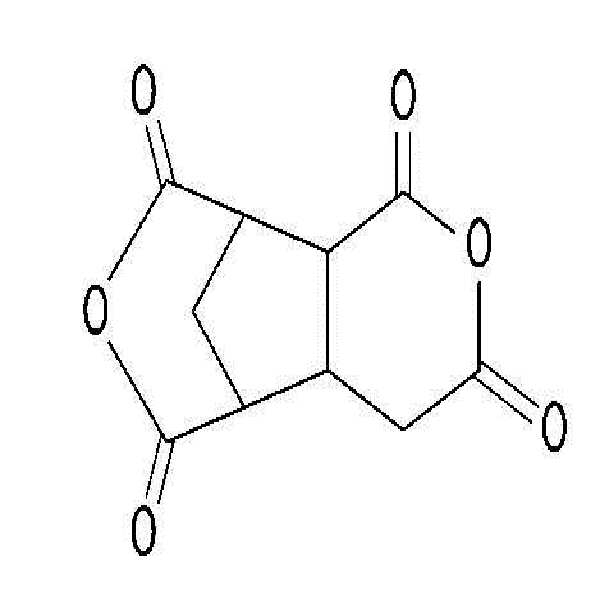
- GTDPSWPPOUPBNX-UHFFFAOYSA-N ac1mqpva Chemical compound CC12C(=O)OC(=O)C1(C)C1(C)C2(C)C(=O)OC1=O GTDPSWPPOUPBNX-UHFFFAOYSA-N 0.000 claims description 14
- 125000003342 alkenyl group Chemical group 0.000 claims description 12
- 230000005684 electric field Effects 0.000 claims description 8
- 125000002723 alicyclic group Chemical group 0.000 claims description 5
- 125000001931 aliphatic group Chemical group 0.000 claims description 5
- 125000004122 cyclic group Chemical group 0.000 claims description 3
- 150000002632 lipids Chemical class 0.000 claims 1
- 229910052709 silver Inorganic materials 0.000 abstract description 7
- 239000004332 silver Substances 0.000 abstract description 7
- 239000010410 layer Substances 0.000 description 52
- 239000010408 film Substances 0.000 description 30
- 238000006243 chemical reaction Methods 0.000 description 20
- 239000003990 capacitor Substances 0.000 description 12
- 229910052751 metal Inorganic materials 0.000 description 10
- 239000002184 metal Substances 0.000 description 10
- 239000004065 semiconductor Substances 0.000 description 9
- 230000000052 comparative effect Effects 0.000 description 8
- 229910052782 aluminium Inorganic materials 0.000 description 7
- XAGFODPZIPBFFR-UHFFFAOYSA-N aluminium Chemical compound [Al] XAGFODPZIPBFFR-UHFFFAOYSA-N 0.000 description 7
- BQCADISMDOOEFD-UHFFFAOYSA-N Silver Chemical compound [Ag] BQCADISMDOOEFD-UHFFFAOYSA-N 0.000 description 6
- 230000001681 protective effect Effects 0.000 description 6
- RYGMFSIKBFXOCR-UHFFFAOYSA-N Copper Chemical compound [Cu] RYGMFSIKBFXOCR-UHFFFAOYSA-N 0.000 description 5
- 229910052802 copper Inorganic materials 0.000 description 5
- 239000010949 copper Substances 0.000 description 5
- 150000002739 metals Chemical class 0.000 description 5
- 206010047571 Visual impairment Diseases 0.000 description 4
- 239000011651 chromium Substances 0.000 description 4
- 238000010586 diagram Methods 0.000 description 4
- 239000000203 mixture Substances 0.000 description 4
- 229920000642 polymer Polymers 0.000 description 4
- 229910000838 Al alloy Inorganic materials 0.000 description 3
- 101150022676 CSTB gene Proteins 0.000 description 3
- VYZAMTAEIAYCRO-UHFFFAOYSA-N Chromium Chemical compound [Cr] VYZAMTAEIAYCRO-UHFFFAOYSA-N 0.000 description 3
- 229910045601 alloy Inorganic materials 0.000 description 3
- 239000000956 alloy Substances 0.000 description 3
- 229910021417 amorphous silicon Inorganic materials 0.000 description 3
- 230000015572 biosynthetic process Effects 0.000 description 3
- 229910052804 chromium Inorganic materials 0.000 description 3
- 101150084890 cstA gene Proteins 0.000 description 3
- 238000005259 measurement Methods 0.000 description 3
- 238000003786 synthesis reaction Methods 0.000 description 3
- 238000002834 transmittance Methods 0.000 description 3
- 229910001316 Ag alloy Inorganic materials 0.000 description 2
- RTZKZFJDLAIYFH-UHFFFAOYSA-N Diethyl ether Chemical compound CCOCC RTZKZFJDLAIYFH-UHFFFAOYSA-N 0.000 description 2
- ZOKXTWBITQBERF-UHFFFAOYSA-N Molybdenum Chemical compound [Mo] ZOKXTWBITQBERF-UHFFFAOYSA-N 0.000 description 2
- 125000004956 cyclohexylene group Chemical group 0.000 description 2
- 239000012535 impurity Substances 0.000 description 2
- 238000012423 maintenance Methods 0.000 description 2
- 239000011572 manganese Substances 0.000 description 2
- 239000012528 membrane Substances 0.000 description 2
- 125000000325 methylidene group Chemical group [H]C([H])=* 0.000 description 2
- 125000000843 phenylene group Chemical group C1(=C(C=CC=C1)*)* 0.000 description 2
- 230000002194 synthesizing effect Effects 0.000 description 2
- 239000010409 thin film Substances 0.000 description 2
- 239000010936 titanium Substances 0.000 description 2
- 229910000599 Cr alloy Inorganic materials 0.000 description 1
- UFHFLCQGNIYNRP-UHFFFAOYSA-N Hydrogen Chemical compound [H][H] UFHFLCQGNIYNRP-UHFFFAOYSA-N 0.000 description 1
- PWHULOQIROXLJO-UHFFFAOYSA-N Manganese Chemical compound [Mn] PWHULOQIROXLJO-UHFFFAOYSA-N 0.000 description 1
- 229910000914 Mn alloy Inorganic materials 0.000 description 1
- 229910001182 Mo alloy Inorganic materials 0.000 description 1
- 229910052581 Si3N4 Inorganic materials 0.000 description 1
- VYPSYNLAJGMNEJ-UHFFFAOYSA-N Silicium dioxide Chemical compound O=[Si]=O VYPSYNLAJGMNEJ-UHFFFAOYSA-N 0.000 description 1
- 229910001362 Ta alloys Inorganic materials 0.000 description 1
- 229910001069 Ti alloy Inorganic materials 0.000 description 1
- RTAQQCXQSZGOHL-UHFFFAOYSA-N Titanium Chemical compound [Ti] RTAQQCXQSZGOHL-UHFFFAOYSA-N 0.000 description 1
- WGLPBDUCMAPZCE-UHFFFAOYSA-N Trioxochromium Chemical compound O=[Cr](=O)=O WGLPBDUCMAPZCE-UHFFFAOYSA-N 0.000 description 1
- 125000003277 amino group Chemical group 0.000 description 1
- 125000003118 aryl group Chemical group 0.000 description 1
- 125000002529 biphenylenyl group Chemical group C1(=CC=CC=2C3=CC=CC=C3C12)* 0.000 description 1
- 239000006227 byproduct Substances 0.000 description 1
- 239000000788 chromium alloy Substances 0.000 description 1
- 229910000423 chromium oxide Inorganic materials 0.000 description 1
- 239000004020 conductor Substances 0.000 description 1
- 229910021419 crystalline silicon Inorganic materials 0.000 description 1
- 230000000694 effects Effects 0.000 description 1
- 150000002148 esters Chemical class 0.000 description 1
- 239000001257 hydrogen Substances 0.000 description 1
- 239000011810 insulating material Substances 0.000 description 1
- 230000014759 maintenance of location Effects 0.000 description 1
- 229910052748 manganese Inorganic materials 0.000 description 1
- 239000011159 matrix material Substances 0.000 description 1
- 125000002496 methyl group Chemical group [H]C([H])([H])* 0.000 description 1
- 229910052750 molybdenum Inorganic materials 0.000 description 1
- 239000011733 molybdenum Substances 0.000 description 1
- 239000011368 organic material Substances 0.000 description 1
- ISWSIDIOOBJBQZ-UHFFFAOYSA-N phenol group Chemical group C1(=CC=CC=C1)O ISWSIDIOOBJBQZ-UHFFFAOYSA-N 0.000 description 1
- 230000000704 physical effect Effects 0.000 description 1
- 230000010287 polarization Effects 0.000 description 1
- 238000006116 polymerization reaction Methods 0.000 description 1
- 229910021332 silicide Inorganic materials 0.000 description 1
- FVBUAEGBCNSCDD-UHFFFAOYSA-N silicide(4-) Chemical compound [Si-4] FVBUAEGBCNSCDD-UHFFFAOYSA-N 0.000 description 1
- HQVNEWCFYHHQES-UHFFFAOYSA-N silicon nitride Chemical compound N12[Si]34N5[Si]62N3[Si]51N64 HQVNEWCFYHHQES-UHFFFAOYSA-N 0.000 description 1
- 229910052814 silicon oxide Inorganic materials 0.000 description 1
- 239000002356 single layer Substances 0.000 description 1
- 238000001308 synthesis method Methods 0.000 description 1
- 229910052715 tantalum Inorganic materials 0.000 description 1
- GUVRBAGPIYLISA-UHFFFAOYSA-N tantalum atom Chemical compound [Ta] GUVRBAGPIYLISA-UHFFFAOYSA-N 0.000 description 1
- 229910052719 titanium Inorganic materials 0.000 description 1
Images


Classifications
-
- C—CHEMISTRY; METALLURGY
- C08—ORGANIC MACROMOLECULAR COMPOUNDS; THEIR PREPARATION OR CHEMICAL WORKING-UP; COMPOSITIONS BASED THEREON
- C08K—Use of inorganic or non-macromolecular organic substances as compounding ingredients
- C08K5/00—Use of organic ingredients
- C08K5/0008—Organic ingredients according to more than one of the "one dot" groups of C08K5/01 - C08K5/59
- C08K5/005—Stabilisers against oxidation, heat, light, ozone
-
- G—PHYSICS
- G02—OPTICS
- G02F—OPTICAL DEVICES OR ARRANGEMENTS FOR THE CONTROL OF LIGHT BY MODIFICATION OF THE OPTICAL PROPERTIES OF THE MEDIA OF THE ELEMENTS INVOLVED THEREIN; NON-LINEAR OPTICS; FREQUENCY-CHANGING OF LIGHT; OPTICAL LOGIC ELEMENTS; OPTICAL ANALOGUE/DIGITAL CONVERTERS
- G02F1/00—Devices or arrangements for the control of the intensity, colour, phase, polarisation or direction of light arriving from an independent light source, e.g. switching, gating or modulating; Non-linear optics
- G02F1/01—Devices or arrangements for the control of the intensity, colour, phase, polarisation or direction of light arriving from an independent light source, e.g. switching, gating or modulating; Non-linear optics for the control of the intensity, phase, polarisation or colour
- G02F1/13—Devices or arrangements for the control of the intensity, colour, phase, polarisation or direction of light arriving from an independent light source, e.g. switching, gating or modulating; Non-linear optics for the control of the intensity, phase, polarisation or colour based on liquid crystals, e.g. single liquid crystal display cells
- G02F1/133—Constructional arrangements; Operation of liquid crystal cells; Circuit arrangements
- G02F1/1333—Constructional arrangements; Manufacturing methods
- G02F1/1337—Surface-induced orientation of the liquid crystal molecules, e.g. by alignment layers
- G02F1/133711—Surface-induced orientation of the liquid crystal molecules, e.g. by alignment layers by organic films, e.g. polymeric films
-
- C—CHEMISTRY; METALLURGY
- C08—ORGANIC MACROMOLECULAR COMPOUNDS; THEIR PREPARATION OR CHEMICAL WORKING-UP; COMPOSITIONS BASED THEREON
- C08G—MACROMOLECULAR COMPOUNDS OBTAINED OTHERWISE THAN BY REACTIONS ONLY INVOLVING UNSATURATED CARBON-TO-CARBON BONDS
- C08G73/00—Macromolecular compounds obtained by reactions forming a linkage containing nitrogen with or without oxygen or carbon in the main chain of the macromolecule, not provided for in groups C08G12/00 - C08G71/00
- C08G73/06—Polycondensates having nitrogen-containing heterocyclic rings in the main chain of the macromolecule
- C08G73/10—Polyimides; Polyester-imides; Polyamide-imides; Polyamide acids or similar polyimide precursors
- C08G73/1003—Preparatory processes
- C08G73/1007—Preparatory processes from tetracarboxylic acids or derivatives and diamines
-
- C—CHEMISTRY; METALLURGY
- C08—ORGANIC MACROMOLECULAR COMPOUNDS; THEIR PREPARATION OR CHEMICAL WORKING-UP; COMPOSITIONS BASED THEREON
- C08K—Use of inorganic or non-macromolecular organic substances as compounding ingredients
- C08K5/00—Use of organic ingredients
- C08K5/04—Oxygen-containing compounds
-
- C—CHEMISTRY; METALLURGY
- C09—DYES; PAINTS; POLISHES; NATURAL RESINS; ADHESIVES; COMPOSITIONS NOT OTHERWISE PROVIDED FOR; APPLICATIONS OF MATERIALS NOT OTHERWISE PROVIDED FOR
- C09K—MATERIALS FOR MISCELLANEOUS APPLICATIONS, NOT PROVIDED FOR ELSEWHERE
- C09K19/00—Liquid crystal materials
- C09K19/04—Liquid crystal materials characterised by the chemical structure of the liquid crystal components, e.g. by a specific unit
- C09K19/06—Non-steroidal liquid crystal compounds
- C09K19/34—Non-steroidal liquid crystal compounds containing at least one heterocyclic ring
- C09K19/3441—Non-steroidal liquid crystal compounds containing at least one heterocyclic ring having nitrogen as hetero atom
- C09K19/3483—Non-steroidal liquid crystal compounds containing at least one heterocyclic ring having nitrogen as hetero atom the heterocyclic ring being a non-aromatic ring
-
- C—CHEMISTRY; METALLURGY
- C09—DYES; PAINTS; POLISHES; NATURAL RESINS; ADHESIVES; COMPOSITIONS NOT OTHERWISE PROVIDED FOR; APPLICATIONS OF MATERIALS NOT OTHERWISE PROVIDED FOR
- C09K—MATERIALS FOR MISCELLANEOUS APPLICATIONS, NOT PROVIDED FOR ELSEWHERE
- C09K19/00—Liquid crystal materials
- C09K19/52—Liquid crystal materials characterised by components which are not liquid crystals, e.g. additives with special physical aspect: solvents, solid particles
- C09K19/54—Additives having no specific mesophase characterised by their chemical composition
- C09K19/56—Aligning agents
-
- C—CHEMISTRY; METALLURGY
- C09—DYES; PAINTS; POLISHES; NATURAL RESINS; ADHESIVES; COMPOSITIONS NOT OTHERWISE PROVIDED FOR; APPLICATIONS OF MATERIALS NOT OTHERWISE PROVIDED FOR
- C09K—MATERIALS FOR MISCELLANEOUS APPLICATIONS, NOT PROVIDED FOR ELSEWHERE
- C09K2323/00—Functional layers of liquid crystal optical display excluding electroactive liquid crystal layer characterised by chemical composition
- C09K2323/02—Alignment layer characterised by chemical composition
- C09K2323/027—Polyimide
-
- G—PHYSICS
- G02—OPTICS
- G02F—OPTICAL DEVICES OR ARRANGEMENTS FOR THE CONTROL OF LIGHT BY MODIFICATION OF THE OPTICAL PROPERTIES OF THE MEDIA OF THE ELEMENTS INVOLVED THEREIN; NON-LINEAR OPTICS; FREQUENCY-CHANGING OF LIGHT; OPTICAL LOGIC ELEMENTS; OPTICAL ANALOGUE/DIGITAL CONVERTERS
- G02F1/00—Devices or arrangements for the control of the intensity, colour, phase, polarisation or direction of light arriving from an independent light source, e.g. switching, gating or modulating; Non-linear optics
- G02F1/01—Devices or arrangements for the control of the intensity, colour, phase, polarisation or direction of light arriving from an independent light source, e.g. switching, gating or modulating; Non-linear optics for the control of the intensity, phase, polarisation or colour
- G02F1/13—Devices or arrangements for the control of the intensity, colour, phase, polarisation or direction of light arriving from an independent light source, e.g. switching, gating or modulating; Non-linear optics for the control of the intensity, phase, polarisation or colour based on liquid crystals, e.g. single liquid crystal display cells
- G02F1/133—Constructional arrangements; Operation of liquid crystal cells; Circuit arrangements
- G02F1/1333—Constructional arrangements; Manufacturing methods
- G02F1/133397—Constructional arrangements; Manufacturing methods for suppressing after-image or image-sticking
-
- G—PHYSICS
- G02—OPTICS
- G02F—OPTICAL DEVICES OR ARRANGEMENTS FOR THE CONTROL OF LIGHT BY MODIFICATION OF THE OPTICAL PROPERTIES OF THE MEDIA OF THE ELEMENTS INVOLVED THEREIN; NON-LINEAR OPTICS; FREQUENCY-CHANGING OF LIGHT; OPTICAL LOGIC ELEMENTS; OPTICAL ANALOGUE/DIGITAL CONVERTERS
- G02F1/00—Devices or arrangements for the control of the intensity, colour, phase, polarisation or direction of light arriving from an independent light source, e.g. switching, gating or modulating; Non-linear optics
- G02F1/01—Devices or arrangements for the control of the intensity, colour, phase, polarisation or direction of light arriving from an independent light source, e.g. switching, gating or modulating; Non-linear optics for the control of the intensity, phase, polarisation or colour
- G02F1/13—Devices or arrangements for the control of the intensity, colour, phase, polarisation or direction of light arriving from an independent light source, e.g. switching, gating or modulating; Non-linear optics for the control of the intensity, phase, polarisation or colour based on liquid crystals, e.g. single liquid crystal display cells
- G02F1/133—Constructional arrangements; Operation of liquid crystal cells; Circuit arrangements
- G02F1/1333—Constructional arrangements; Manufacturing methods
- G02F1/1337—Surface-induced orientation of the liquid crystal molecules, e.g. by alignment layers
- G02F1/133707—Structures for producing distorted electric fields, e.g. bumps, protrusions, recesses, slits in pixel electrodes
-
- G—PHYSICS
- G02—OPTICS
- G02F—OPTICAL DEVICES OR ARRANGEMENTS FOR THE CONTROL OF LIGHT BY MODIFICATION OF THE OPTICAL PROPERTIES OF THE MEDIA OF THE ELEMENTS INVOLVED THEREIN; NON-LINEAR OPTICS; FREQUENCY-CHANGING OF LIGHT; OPTICAL LOGIC ELEMENTS; OPTICAL ANALOGUE/DIGITAL CONVERTERS
- G02F1/00—Devices or arrangements for the control of the intensity, colour, phase, polarisation or direction of light arriving from an independent light source, e.g. switching, gating or modulating; Non-linear optics
- G02F1/01—Devices or arrangements for the control of the intensity, colour, phase, polarisation or direction of light arriving from an independent light source, e.g. switching, gating or modulating; Non-linear optics for the control of the intensity, phase, polarisation or colour
- G02F1/13—Devices or arrangements for the control of the intensity, colour, phase, polarisation or direction of light arriving from an independent light source, e.g. switching, gating or modulating; Non-linear optics for the control of the intensity, phase, polarisation or colour based on liquid crystals, e.g. single liquid crystal display cells
- G02F1/133—Constructional arrangements; Operation of liquid crystal cells; Circuit arrangements
- G02F1/1333—Constructional arrangements; Manufacturing methods
- G02F1/1337—Surface-induced orientation of the liquid crystal molecules, e.g. by alignment layers
- G02F1/133711—Surface-induced orientation of the liquid crystal molecules, e.g. by alignment layers by organic films, e.g. polymeric films
- G02F1/133723—Polyimide, polyamide-imide
Landscapes
- Chemical & Material Sciences (AREA)
- Physics & Mathematics (AREA)
- Crystallography & Structural Chemistry (AREA)
- Nonlinear Science (AREA)
- Organic Chemistry (AREA)
- Materials Engineering (AREA)
- Engineering & Computer Science (AREA)
- Spectroscopy & Molecular Physics (AREA)
- Mathematical Physics (AREA)
- General Physics & Mathematics (AREA)
- Optics & Photonics (AREA)
- Health & Medical Sciences (AREA)
- Chemical Kinetics & Catalysis (AREA)
- Medicinal Chemistry (AREA)
- Polymers & Plastics (AREA)
- Liquid Crystal (AREA)
Abstract
본 발명은 하기 화학식 1 및 하기 화학식 2로 표현되는 광안정제 중 적어도 하나를 포함하는 배향막을 제공한다:


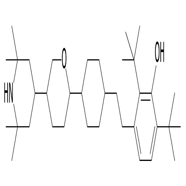
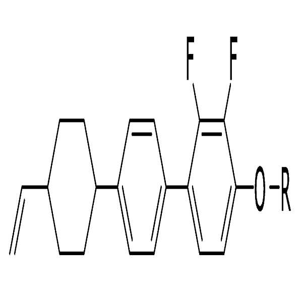
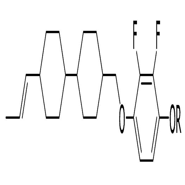
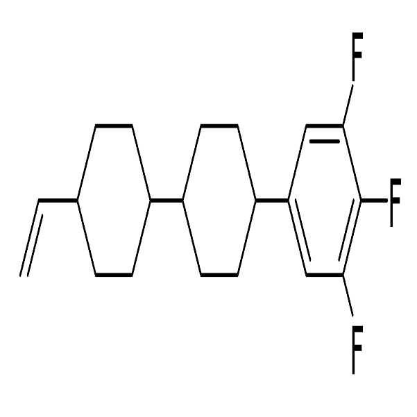
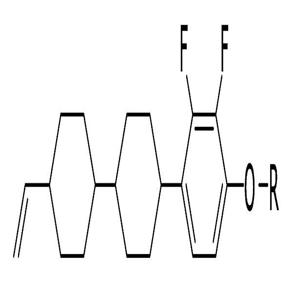
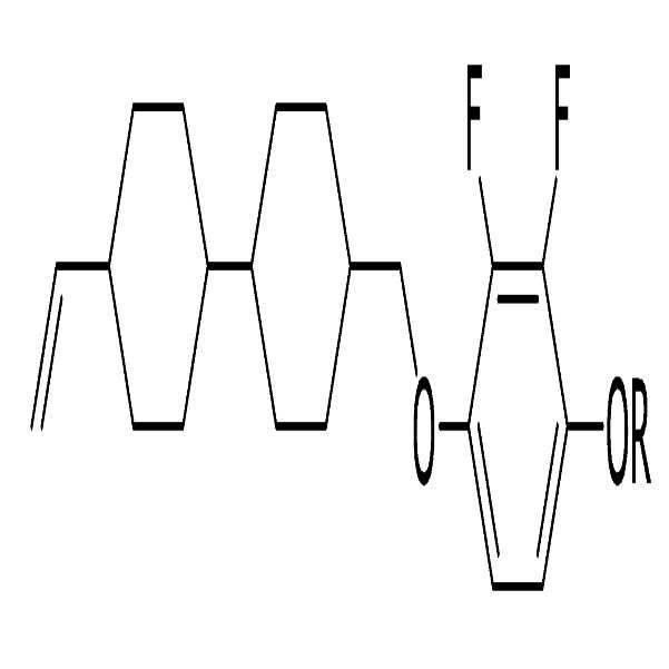
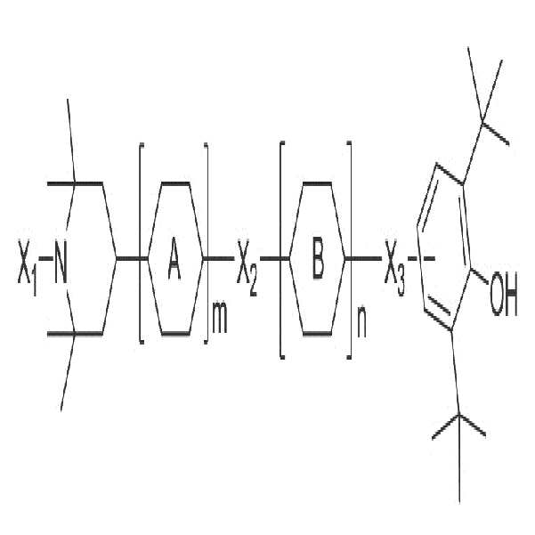
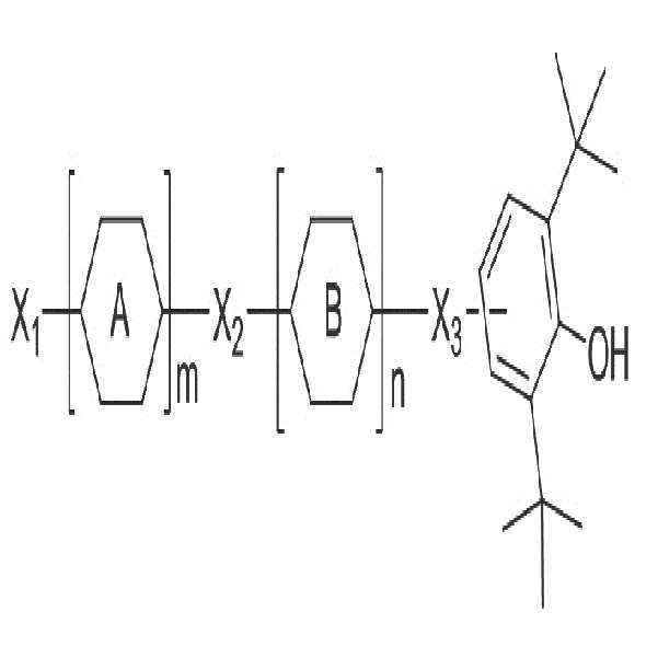
여기서, 상기 X1은 H, O, OR 및 R 중 어느 하나이고, 상기 X2는 O, OCO, OR, RO, NOR, 및 R 중 어느 하나이고, 상기 X3은 O, OCO, OR, RO, NOR 및 R 중 어느 하나이고, 상기 A 및 B는 각각 독립적으로 시클로헥실기, 시클릭에테르기 및 페닐기 중 어느 하나 이상을 포함하고, 상기 R은 탄소수 1 내지 5의 알킬기이며, 상기 m 및 n은 각각 독립적으로 0 내지 2의 자연수이다.The present invention provides an alignment film comprising at least one of the light stabilizers represented by the following Chemical Formulas 1 and 2:
Here, the XOneIs any one of H, O, OR and R, and X2Is any one of O, OCO, OR, RO, NOR, and R, and X3silver Wherein each of A and B independently represents any one or more of a cyclohexyl group, a cyclic ether group and a phenyl group, and R is an alkylene group having 1 to 5 carbon atoms Alkyl group, and m and n are each independently a natural number of 0 to 2.
Description
본 발명은 배향막 및 이를 포함하는 액정 표시 장치에 관한 것이다.The present invention relates to an alignment film and a liquid crystal display device including the same.
액정 표시 장치(liquid crystal display, LCD)는 현재 가장 널리 사용되고 있는 평판 표시 장치(flat panel display) 중 하나이다. 액정 표시 장치는 전기장 생성 전극이 형성되어 있는 두 장의 표시판과 그 사이에 들어 있는 액정층을 포함하며, 전기장 생성 전극에 전압을 인가하여 액정층에 전기장을 생성함으로써 액정층의 액정 분자들의 방향을 결정하고 액정층을 통과하는 빛의 투과율을 조절한다.BACKGROUND ART [0002] Liquid crystal displays (LCDs) are one of the most widely used flat panel displays. The liquid crystal display device includes two display panels on which an electric field generating electrode is formed and a liquid crystal layer interposed therebetween. A voltage is applied to the electric field generating electrode to generate an electric field in the liquid crystal layer to determine the direction of the liquid crystal molecules in the liquid crystal layer And controls the transmittance of light passing through the liquid crystal layer.
액정 표시 장치에서 액정은 빛의 투과율을 조절하여 원하는 화상을 얻는데 매우 중요하다. 특히, 액정 표시 장치의 용도가 다양화됨에 따라, 저전압 구동, 높은 전압 보전율(voltage holding ratio, VHR), 넓은 시야각 특성, 넓은 동작 온도 범위, 낮은 잔상(afterimage) 및 고속 응답성 등의 다양한 특성이 요구된다.In a liquid crystal display, liquid crystal is very important for controlling a light transmittance to obtain a desired image. Especially, as the use of liquid crystal display devices is diversified, various characteristics such as low voltage driving, high voltage holding ratio (VHR), wide viewing angle characteristic, wide operating temperature range, low afterimage and high speed response Is required.
본 발명이 해결하고자 하는 기술적 과제는 광안정제(photostabilizer)를 포함하는 배향막을 통해 잔상 및 신뢰성이 개선될 수 있는 배향막 및 이를 포함하는 액정 표시 장치를 제공하는 것이다.SUMMARY OF THE INVENTION The present invention provides an alignment film capable of improving afterimage and reliability through an alignment film including a photostabilizer, and a liquid crystal display device including the alignment film.
이러한 과제를 해결하기 위하여 본 발명의 일실시예에 따르면, 하기 화학식 1 및 하기 화학식 2로 표현되는 광안정제 중 적어도 하나를 포함하는 배향막을 제공한다. According to an embodiment of the present invention, there is provided an alignment layer comprising at least one of a light stabilizer represented by Chemical Formula 1 and Chemical Formula 2 below.


여기서, 상기 X1은 H, O, OR 및 R 중 어느 하나이고, 상기 X2는 O, OCO, OR, RO, NOR, 및 R 중 어느 하나이고, 상기 X3은 O, OCO, OR, RO, NOR 및 R 중 어느 하나이고, 상기 A 및 B는 각각 독립적으로 시클로헥실기, 시클릭에테르기 및 페닐기 중 어느 하나 이상을 포함하고, 상기 R은 탄소수 1 내지 5의 알킬기이며, 상기 m 및 n은 각각 독립적으로 0 내지 2의 자연수이다.Here, the X 1 is H, O, and OR, and any one of R, wherein X 2 is O, OCO, OR, RO, NOR, and R is any one of, wherein X 3 is Wherein each of A and B independently represents any one or more of a cyclohexyl group, a cyclic ether group and a phenyl group, and R is an alkylene group having 1 to 5 carbon atoms Alkyl group, and m and n are each independently a natural number of 0 to 2.
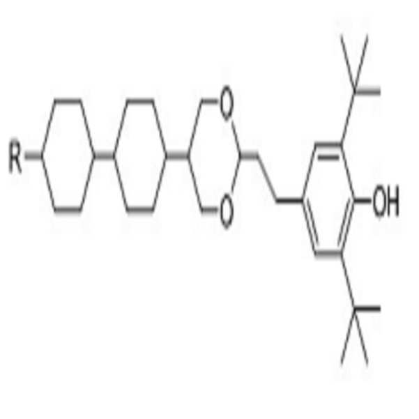
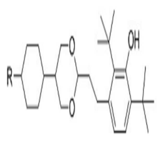
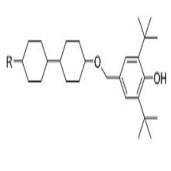
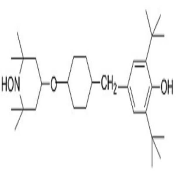
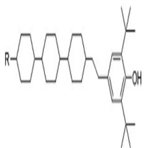
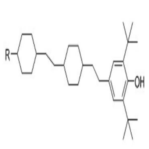
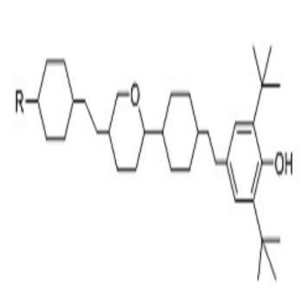
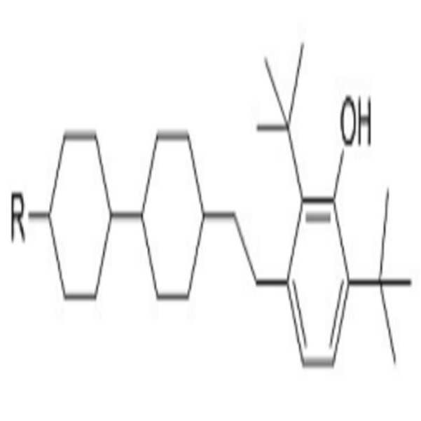
상기 화학식 1로 표현되는 광안정제는 하기 화학식 1-1 내지 화학식 1-28로 표현되는 화합물 중 적어도 하나를 포함할 수 있다.The light stabilizer represented by Formula 1 may include at least one compound represented by Formula 1-1 to Formula 1-28.


여기서, 상기 R은 탄소수 1 내지 5의 알킬기이다.Here, R is an alkyl group having 1 to 5 carbon atoms.
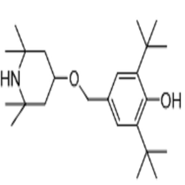
상기 화학식 2로 표현되는 광안정제는 하기 화학식 2-1 내지 화학식 2-16으로 표현되는 화합물 중 적어도 하나를 포함할 수 있다.The light stabilizer represented by Formula 2 may include at least one compound represented by Formula 2-1 to Formula 2-16 below.


여기서, 상기 R은 탄소수 1 내지 5의 알킬기이다.Here, R is an alkyl group having 1 to 5 carbon atoms.
상기 배향막은 이무수물(dianhydride)계 단분자를 포함하는 제1 물질, 및Wherein the alignment layer comprises a first material comprising dianhydride monomers,
디아민(diamine)계 단분자를 포함하는 제2 물질을 더 포함할 수 있다.And a second substance containing a diamine-based monomolecule.
상기 광안정제는 상기 디아민계 단분자에 결합되어 있을 수 있다.The light stabilizer may be bonded to the diamine monomers.
상기 제1 물질은 지방고리족 이무수물(alicyclic dianhydride)계 단분자를 포함하고, 상기 제2 물질은 방향족 디아민(aromatic diamine)계 단분자, 지방족 고리 치환 방향족 디아민(aliphatic ring substituted aromatic diamine)계 단분자, 광반응성 디아민계 단분자, 알킬화 방향족 디아민계 단분자 중 적어도 하나 이상을 포함할 수 있다.Wherein the first material comprises an alicyclic dianhydride monomolecule and the second material is an aromatic diamine monomolecule, an aliphatic ring substituted aromatic diamine, Molecule, a photoreactive diamine-based monomer, and an alkylated aromatic diamine-based monomer.
상기 지방고리족 이무수물계 단분자는 하기 화학식 3-1 내지 화학식 3-5로 표현되는 단분자 중 적어도 하나를 포함할 수 있다.The fatty cyclic dianhydride monomers may include at least one of monomers represented by the following formulas (3-1) to (3-5).


또한, 본 발명의 다른 실시예에 따르면, 제1 기판, 상기 제1 기판과 마주보는 제2 기판, 상기 제1 기판 및 상기 제2 기판 중 적어도 어느 하나의 기판 상에 형성된 전기장 생성 전극, 상기 제1 기판 상에 형성된 제1 배향막 및 상기 제2 기판 상에 형성된 제2 배향막, 및 상기 제1 기판과 상기 제2 기판 사이에 개재된 복수의 액정 분자들로 형성된 액정층을 포함하고, 상기 제1 배향막 및 상기 제2 배향막 중 적어도 어느 하나는 하기 화학식 1 및 하기 화학식 2로 표현되는 광안정제 중 적어도 하나를 포함하는 액정 표시 장치를 제공한다.According to another embodiment of the present invention, there is provided a plasma display panel comprising a first substrate, a second substrate facing the first substrate, an electric field generating electrode formed on at least one of the first substrate and the second substrate, 1. A liquid crystal display device comprising a liquid crystal layer formed of a first alignment film formed on a substrate and a second alignment film formed on the second substrate and a plurality of liquid crystal molecules interposed between the first substrate and the second substrate, And at least one of the alignment layer and the second alignment layer includes at least one of a light stabilizer represented by the following general formulas (1) and (2).


여기서, 상기 X1은 H, O, OR 및 R 중 어느 하나이고, 상기 X2는 O, OCO, OR, RO, NOR, 및 R 중 어느 하나이고, 상기 X3은 O, OCO, OR, RO, NOR 및 R 중 어느 하나이고, 상기 A 및 B는 각각 독립적으로 시클로헥실기, 시클릭에테르기 및 페닐기 중 어느 하나 이상을 포함하고, 상기 R은 탄소수 1 내지 5의 알킬기이며, 상기 m 및 n은 각각 독립적으로 0 내지 2의 자연수이다.Here, the X 1 is H, O, and OR, and any one of R, wherein X 2 is O, OCO, OR, RO, NOR, and R is any one of, wherein X 3 is Wherein each of A and B independently represents any one or more of a cyclohexyl group, a cyclic ether group and a phenyl group, and R is an alkylene group having 1 to 5 carbon atoms Alkyl group, and m and n are each independently a natural number of 0 to 2.
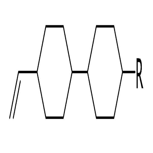
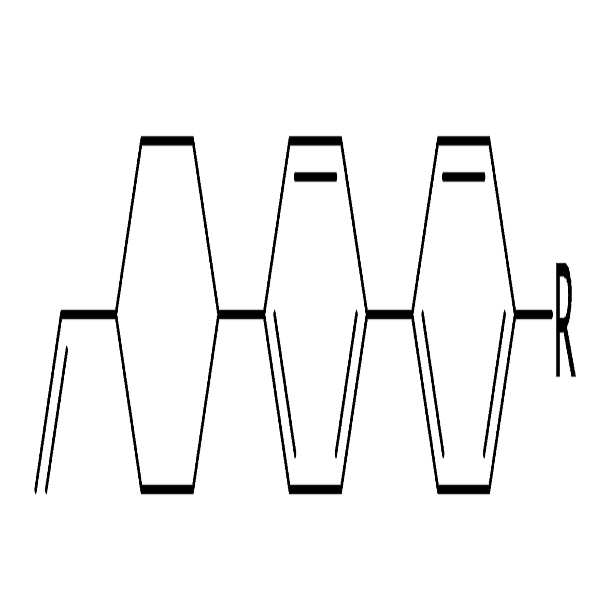
상기 액정 분자는 알케닐(alkenyl)기를 포함할 수 있다.The liquid crystal molecule may include an alkenyl group.
상기 알케닐기는 하기 화학식 8-1 내지 화학식 8-16으로 표현되는 화합물 중 적어도 하나를 포함할 수 있다. The alkenyl group may include at least one of the compounds represented by the following formulas (8-1) to (8-16).


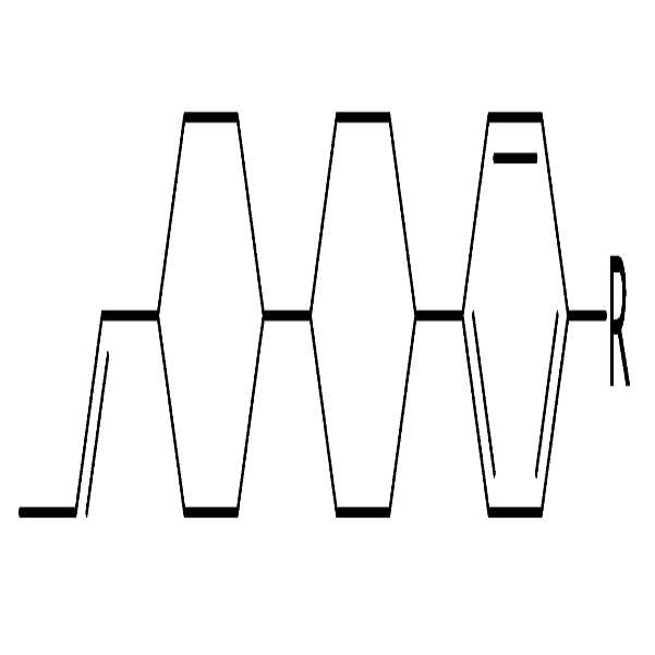


여기서, R은 탄소수 1 내지 5의 알킬기이다.Here, R is an alkyl group having 1 to 5 carbon atoms.
이상과 같이 본 발명의 일 실시예에 따른 배향막 및 이를 포함하는 액정 표시 장치는 배향막에 신규 광안정제를 포함하고 있어 액정 조성물에서 발생할 수 있는 불순물의 발생을 방지하여 표시 패널에서 발생할 수 있는 잔상 및 신뢰성이 개선될 수 있다.As described above, the alignment layer and the liquid crystal display device including the same according to an embodiment of the present invention include a novel light stabilizer in the alignment layer to prevent the generation of impurities that may occur in the liquid crystal composition, Can be improved.
도 1은 본 발명의 일 실시예에 따른 액정 표시 장치의 화소에 대한 등가 회로도이다.
도 2는 본 발명의 일 실시예에 따른 액정 표시 장치의 배치도이다.
도 3은 도 2의 III-III 선을 따라 자른 단면도이다.
도 4는
본 발명의 일 실시예 및 비교예에 따른 액정 표시 장치의 전압 보전율을 측정한 결과를 나타낸 그래프이다.1 is an equivalent circuit diagram of a pixel of a liquid crystal display according to an exemplary embodiment of the present invention.
2 is a layout diagram of a liquid crystal display device according to an embodiment of the present invention.
3 is a cross-sectional view taken along line III-III in FIG.
4 is a graph showing the results of measurement of the voltage holding ratio of the liquid crystal display device according to an embodiment of the present invention and a comparative example.
첨부한 도면을 참고로 하여 본 발명의 실시예에 대하여 본 발명이 속하는 기술 분야에서 통상의 지식을 가진 자가 용이하게 실시할 수 있도록 상세히 설명한다. 그러나 본 발명은 여러 가지 상이한 형태로 구현될 수 있으며 여기에서 설명하는 실시예에 한정되지 않는다.BRIEF DESCRIPTION OF THE DRAWINGS The above and other features and advantages of the present invention will become more apparent by describing in detail exemplary embodiments thereof with reference to the attached drawings in which: FIG. The present invention may, however, be embodied in many different forms and should not be construed as limited to the embodiments set forth herein.
도면에서 여러 층 및 영역을 명확하게 표현하기 위하여 두께를 확대하여 나타내었다. 명세서 전체를 통하여 유사한 부분에 대해서는 동일한 도면 부호를 붙였다. 층, 막, 영역, 판 등의 부분이 다른 부분 "위에" 있다고 할 때, 이는 다른 부분 "바로 위에" 있는 경우뿐 아니라 그 중간에 또 다른 부분이 있는 경우도 포함한다. 반대로 어떤 부분이 다른 부분 "바로 위에" 있다고 할 때에는 중간에 다른 부분이 없는 것을 뜻한다.In the drawings, the thickness is enlarged to clearly represent the layers and regions. Like parts are designated with like reference numerals throughout the specification. It will be understood that when an element such as a layer, film, region, plate, or the like is referred to as being "on" another portion, it includes not only the element directly over another element, Conversely, when a part is "directly over" another part, it means that there is no other part in the middle.
이하, 도 1 내지 도 3을 참고하여 본 발명의 일 실시예에 따른 액정 표시 장치에 대해서 상세하게 설명한다.Hereinafter, a liquid crystal display according to an embodiment of the present invention will be described in detail with reference to FIGS. 1 to 3. FIG.
도 1은 본 발명의 일 실시예에 따른 액정 표시 장치의 화소에 대한 등가 회로도이고, 도 2는 본 발명의 일 실시예에 따른 액정 표시 장치의 배치도이며, 도 3은 도 2의 III-III 선을 따라 자른 단면도이다.FIG. 1 is an equivalent circuit diagram of a pixel of a liquid crystal display device according to an embodiment of the present invention. FIG. 2 is a layout diagram of a liquid crystal display device according to an embodiment of the present invention. Fig.
먼저 도 1을 참고하면, 본 발명의 일 실시예에 따른 액정 표시 장치는 서로 마주하는 하부 표시판(100)과 상부 표시판(200), 그리고 그 사이에 개재되어 있는 액정층(3)을 포함한다.Referring first to FIG. 1, a liquid crystal display device according to an embodiment of the present invention includes a
액정 표시 장치는 복수의 게이트선(GL), 복수 쌍의 데이터선(DLa, DLb) 및 복수의 유지 전극선(SL)을 포함하는 신호선과 이에 연결된 복수의 화소(PX)를 포함한다.The liquid crystal display device includes a signal line including a plurality of gate lines GL, a plurality of data lines DLa and DLb and a plurality of sustain electrode lines SL and a plurality of pixels PX connected thereto.
각 화소(PX)는 한 쌍의 부화소(PXa, PXb)를 포함하며, 부화소(PXa, PXb)는 스위칭 소자(Qa, Qb)와 액정 축전기(Clca, Clcb) 및 유지 축전기(storage capacitor)(Csta, Cstb)를 포함한다.Each pixel PX includes a pair of subpixels PXa and PXb and the subpixels PXa and PXb are connected to the switching elements Qa and Qb and liquid crystal capacitors Clca and Clcb and a storage capacitor, (Csta, Cstb).
스위칭 소자(Qa, Qb)는 하부 표시판(100)에 구비되어 있는 박막 트랜지스터 등의 삼단자 소자로서, 그 제어 단자는 게이트선(GL)과 연결되어 있고, 입력 단자는 데이터선(DLa, DLb)과 연결되어 있으며, 출력 단자는 액정 축전기(Clca, Clcb) 및 유지 축전기(Csta, Cstb)와 연결되어 있다.The switching elements Qa and Qb are three terminal elements such as a thin film transistor provided on the
액정 축전기(Clca, Clcb)는 부화소 전극(191a, 191b)과 공통 전극(270)을 두 단자로 하고, 두 단자 사이의 액정층(3) 부분을 유전체로 하여 형성된다.The liquid crystal capacitors Clca and Clcb are formed by using the
액정 축전기(Clca, Clcb)의 보조적인 역할을 하는 유지 축전기(Csta, Cstb)는 하부 표시판(100)에 구비된 유지 전극선(SL)과 부화소 전극(191a, 191b)이 절연체를 사이에 두고 중첩되어 이루어지며 유지 전극선(SL)에는 공통 전압(Vcom) 따위의 정해진 전압이 인가된다.The storage capacitors Csta and Cstb serving as auxiliary capacitors of the liquid crystal capacitors Clca and Clcb are formed by stacking the sustain electrode lines SL and the
두 액정 축전기(Clca, Clcb)에 충전되는 전압은 서로 약간의 차이가 나도록 설정되어 있다. 예를 들면, 액정 축전기(Clca)에 인가되는 데이터 전압이 인접한 다른 액정 축전기(Clcb)에 인가되는 데이터 전압에 비하여 항상 낮거나 높도록 설정한다. 이렇게 두 액정 축전기(Clca, Clcb)의 전압을 적절하게 조절하면 측면에서 바라보는 영상이 정면에서 바라보는 영상에 근접하도록 할 수 있어 액정 표시 장치의 측면 시인성이 향상된다.The voltages charged in the two liquid crystal capacitors (Clca, Clcb) are set so as to slightly differ from each other. For example, the data voltage applied to the liquid crystal capacitor Clca is set to be always lower or higher than the data voltage applied to the adjacent liquid crystal capacitor Clcb. By appropriately adjusting the voltage of the two liquid crystal capacitors Clca and Clcb, the image viewed from the side can be brought close to the image viewed from the front, thereby improving the lateral visibility of the liquid crystal display device.
이하에서, 도 2 및 도 3을 참고하여 본 발명의 일 실시예에 따른 액정 표시 장치에 대해 더욱 상세하게 설명한다.Hereinafter, a liquid crystal display according to an embodiment of the present invention will be described in more detail with reference to FIGS. 2 and 3. FIG.
도 2 및 도 3을 참고하면, 본 발명의 일 실시예에 따른 액정 표시 장치는 서로 마주하는 하부 표시판(100)과 상부 표시판(200) 및 이들 두 표시판(100, 200) 사이에 들어 있는 액정층(3)을 포함한다.2 and 3, a liquid crystal display device according to an embodiment of the present invention includes a
먼저, 하부 표시판(100)에 대하여 설명한다.First, the
절연 기판(110) 위에 복수의 게이트선(gate line)(121) 및 복수의 유지 전극선(storage electrode line)(131, 135)이 형성되어 있다.A plurality of
게이트선(121)은 게이트 신호를 전달하며 주로 가로 방향으로 뻗어 있다. 각 게이트선(121)은 위로 돌출한 복수의 제1 및 제2 게이트 전극(124a, 124b)을 포함한다.The
유지 전극선은 게이트선(121)과 실질적으로 나란하게 뻗은 줄기선(stem)(131)과 이로부터 뻗어 나온 복수의 유지 전극(135)을 포함한다. 유지 전극선(131, 135)의 모양 및 배치는 여러 형태로 변형될 수 있다.The sustain electrode line includes a
게이트선(121) 및 유지 전극선(131, 135)은 알루미늄(Al)과 알루미늄 합금 등 알루미늄 계열의 금속, 은(Ag)과 은 합금 등 은 계열의 금속, 구리(Cu)와 구리 합금 등 구리 계열의 금속으로 이루어진 일군에서 선택된 적어도 하나로 형성될 수 있다.The
본 실시예에서 게이트선(121) 및 게이트 전극(124a, 124b)이 단일막으로 형성되는 것으로 설명하였으나, 이에 한정되지 않고, 이중막 또는 삼중막 형태 등으로 형성될 수 있다.In the present embodiment, the
이중막 구조를 갖는 경우, 게이트선(121) 및 게이트 전극(124a, 124b)은 하부막 및 상부막으로 형성될 수 있고, 하부막은 몰리브덴(Mo)과 몰리브덴 합금 등 몰리브덴 계열의 금속, 크롬(Cr), 크롬 합금, 티타늄(Ti), 티타늄 합금, 탄탈늄(Ta), 탄탈늄 합금, 망간(Mn), 망간 합금으로 이루어진 일군에서 선택된 적어도 하나로 형성될 수 있다. 상부막은 알루미늄(Al)과 알루미늄 합금 등 알루미늄 계열의 금속, 은(Ag)과 은 합금 등 은 계열의 금속, 구리(Cu)와 구리 합금 등 구리 계열의 금속으로 이루어진 일군에서 선택된 적어도 하나로 형성될 수 있다. 삼중막 구조의 경우, 서로 물리적 성질이 다른 막들이 조합되어 형성될 수 있다.The
게이트선(121) 및 유지 전극선(131, 135) 위에는 게이트 절연막 (140)이 형성되어 있으며, 게이트 절연막(140) 위에는 비정질 또는 결정질 규소 등으로 만들어진 복수의 반도체층(154a, 154b)가 형성되어 있다.A
반도체층(154a, 154b) 위에는 각각 복수 쌍의 저항성 접촉 부재 (163b, 165b)가 형성되어 있으며, 저항성 접촉 부재(163b, 165b)는 실리사이드(silicide) 또는 n형 불순물이 고농도로 도핑되어 있는 n+ 수소화 비정질 규소 따위의 물질로 만들어질 수 있다.A plurality of pairs of
저항성 접촉 부재(163b, 165b) 및 게이트 절연막(140) 위에는 복수 쌍의 데이터선 (171a, 171b)과 복수 쌍의 제1 및 제2 드레인 전극 (175a, 175b)이 형성되어 있다.A plurality of pairs of
데이터선(171a, 171b)은 데이터 신호를 전달하며 주로 세로 방향으로 뻗어 게이트선(121) 및 유지 전극선의 줄기선(131)과 교차한다. 데이터선(171a, 171b)은 제1, 제2 게이트 전극(124a, 124b)을 향하여 뻗어 U자형으로 굽은 제1 및 제2 소스 전극(source electrode)(173a, 173b)을 포함하며, 제1 및 제2 소스 전극(173a, 173b)은 제1, 제2 게이트 전극(124a, 124b)을 중심으로 제1 및 제2 드레인 전극(175a, 175b)과 마주한다.The
데이터선(171a, 171b)은 알루미늄(Al)과 알루미늄 합금 등 알루미늄 계열의 금속, 은(Ag)과 은 합금 등 은 계열의 금속, 구리(Cu)와 구리 합금 등 구리 계열의 금속으로 이루어진 일군에서 선택된 적어도 하나로 형성될 수 있다. 본 실시예에서 데이터선(171a, 171b)이 단일막으로 형성되는 것으로 설명하였으나, 이에 한정되지 않고, 이중막 또는 삼중막 형태 등으로 형성될 수 있다.The
제1 및 제2 드레인 전극(175a, 175b)은 각각 제1 및 제2 소스 전극(173a, 173b)으로 일부 둘러싸인 한 쪽 끝에서부터 위로 뻗어 있으며 반대쪽 끝은 다른 층과의 접속을 위해 면적이 넓을 수 있다.The first and
그러나 제1 및 제2 드레인 전극(175a, 175b)을 비롯한 데이터선(171a, 171b)의 모양 및 배치는 여러 형태로 변형될 수 있다.However, the shapes and arrangements of the
제1 및 제2 게이트 전극(124a, 124b), 제1 및 제2 소스 전극(173a, 173b) 및 제1 및 제2 드레인 전극(175a, 175b)은 제1 및 제2 반도체층(154a, 154b)와 함께 제1 및 제2 박막 트랜지스터를 이루며, 제1 및 제2 박막 트랜지스터의 채널(channel)은 제1 및 제2 소스 전극(173a, 173b)과 제1 및 제2 드레인 전극(175a, 175b) 사이의 제1 및 제2 반도체층(154a, 154b)에 형성된다.The first and
저항성 접촉 부재(163b, 165b)는 그 아래의 반도체층(154a, 154b)와 그 위의 데이터선(171a, 171b), 드레인 전극(175a, 175b) 사이에만 존재하며 이들 사이의 접촉 저항을 낮추어 준다. 반도체층(154a, 154b)에는 소스 전극(173a, 173b)과 드레인 전극(175a, 175b) 사이에는 데이터선(171a, 171b) 및 드레인 전극(175a, 175b)으로 가리지 않고 노출된 부분이 있다.The
데이터선(171a, 171b), 드레인 전극(175a, 175b) 및 노출된 반도체층(154a, 154b) 부분 위에는 질화규소 또는 산화규소 따위로 만들어진 하부 보호막(180p)이 형성되어 있다.A lower
하부 보호막(180p) 위에는 색필터(230)가 형성되어 있다. 색필터(230)는 적색, 녹색, 청색의 3색 컬러 필터를 포함할 수 있다. 색필터(230) 위에 크롬 및 크롬 산화물의 단일층이나 이중층 또는 유기 물질로 이루어진 차광 부재(220)가 형성되어 있다. 차광 부재(220)는 매트릭스 형태로 배열되어 있는 개구부를 가질 수 있다.A
색필터(230)와 차광 부재(220) 위에는 투명한 유기 절연 물질로 이루어진 상부 보호막(180q)이 형성되어 있다. 상부 보호막(180q)은 색필터(230)가 노출되는 것을 방지하고 평탄면을 제공한다. 상부 보호막(180q)에는 제1 및 제2 드레인 전극(175a, 175b)을 드러내는 복수의 접촉 구멍(185a, 185b)이 형성되어 있다.An upper
상부 보호막(180q) 위에는 복수의 화소 전극 (191)이 형성되어 있다. 화소 전극(191)은 ITO 또는 IZO 등의 투명한 도전 물질이나 알루미늄, 은, 크롬 또는 그 합금 등의 반사성 금속으로 만들어질 수 있다.A plurality of
각 화소 전극(191)은 서로 분리되어 있는 제1 및 제2 부화소 전극(191a, 191b)을 포함하며, 제1 및 제2 부화소 전극(191a, 191b)은 각각 가로 줄기부(192) 및 이와 교차하는 세로 줄기부(193)로 이루어진 십자형 줄기부를 포함하고, 가로 줄기부(192) 및 세로 줄기부(193)에서 비스듬하게 뻗어 나온 미세 가지부(194)를 포함한다.Each of the
하부 표시판(100)의 안쪽 면에는 제1 배향막(11)이 형성되어 있으며, 제1 배향막(11)은 수직 배향막일 수 있다. 제1 배향막(11)은 배향 보조제를 광조사하여 형성된 제1 배향 중합체(13a)를 포함한다. 배향 보조제는 반응성 메소겐(Reactive Mesogen)일 수 있다. 제1 배향막(11)을 형성하기 위해 제1 배향 물질을 하부 표시판(100)에 도포할 때, 배향 보조제는 제1 배향 물질과 혼합되어 하부 표시판(100)에 도포될 수 있다.A
본 실시예에서 제1 배향막(11)은 이무수물(dianhydride)계 단분자(monomer), 디아민(diamine)계 단분자 및 디아민에 결합되어 있는 광안정제를 포함할 수 있다.In this embodiment, the
여기서, 이무수물(dianhydride)계 단분자(monomer)로서 지방고리족 이무수물(alicyclic dianhydride)계 단분자를 포함할 수 있으며, 디아민(diamine)계 단분자로는 방향족 디아민(aromatic diamine)계 단분자, 지방족 고리 치환 방향족 디아민(aliphatic ring substituted aromatic diamine)계 단분자, 광반응성 디아민계 단분자, 알킬화 방향족 디아민계 단분자 중 적어도 하나 이상을 포함할 수 있다.Here, dianhydride monomers may include alicyclic dianhydride monomers, and diamine monomers include aromatic diamine monomers such as monomolecular monomers, , An aliphatic ring-substituted aromatic diamine-based mono-molecule, a photoreactive diamine-based mono-molecule, and an alkylated aromatic diamine-based mono-molecule.
본 실시예에 따른 제1 배향막(11)에 포함되어 있는 광안정제는 하기 화학식 1 및 화학식 2로 표현되는 화합물 중 적어도 하나 이상을 포함한다.The light stabilizer contained in the


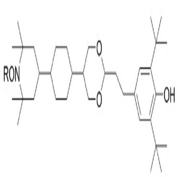
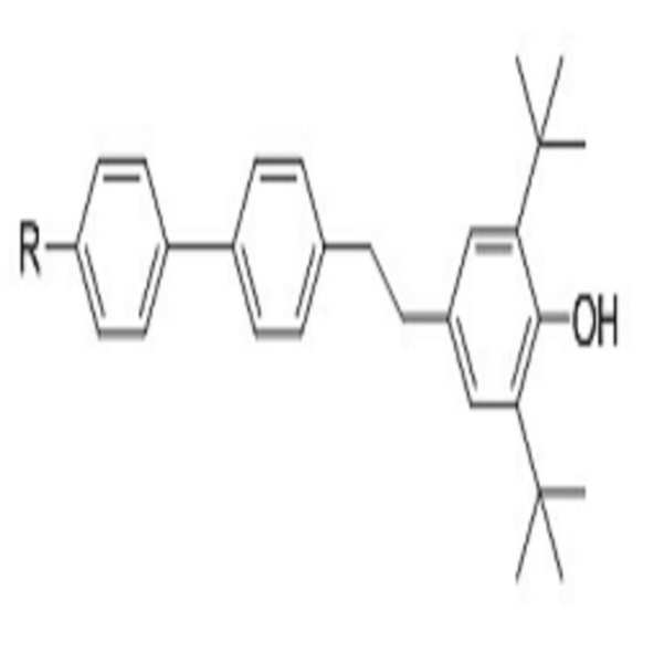
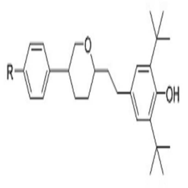
여기서, 상기 X1은 H, O, OR 및 R 중 어느 하나이고, 상기 X2는 O, OCO, OR, RO, NOR, 및 R 중 어느 하나이고, 상기 X3은 O, OCO, OR, RO, NOR 및 R 중 어느 하나이고, 상기 A 및 B는 각각 독립적으로 시클로헥실기, 시클릭에테르기 및 페닐기 중 어느 하나 이상을 포함하고, 상기 R은 탄소수 1 내지 5의 알킬기이며, 상기 m 및 n은 각각 독립적으로 0 내지 2의 자연수이다.Here, the X 1 is H, O, and OR, and any one of R, wherein X 2 is O, OCO, OR, RO, NOR, and R is any one of, wherein X 3 is Wherein each of A and B independently represents any one or more of a cyclohexyl group, a cyclic ether group and a phenyl group, and R is an alkylene group having 1 to 5 carbon atoms Alkyl group, and m and n are each independently a natural number of 0 to 2.
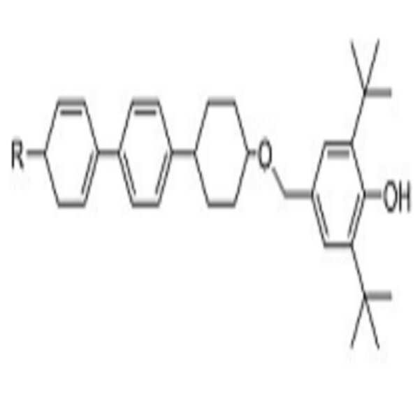
상기 X3는 화학식 1 및 화학식 2의 우측에 연결된 페놀기의 파라(para) 또는 메타(meta) 위치에 위치할 수 있으며, 화학식 1의 좌측에 연결되는 시클로아민기를 포함한다.X 3 may be located at the para or meta position of the phenol group connected to the right side of the general formulas (1) and (2), and includes a cyclic amine group connected to the left side of the general formula (1).
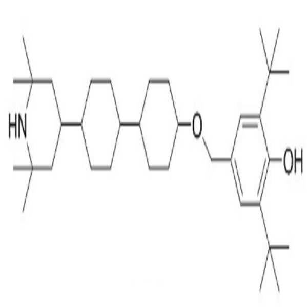
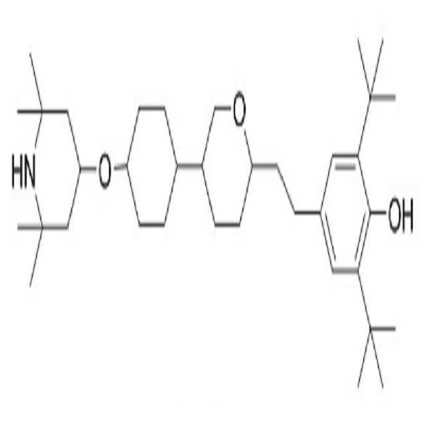
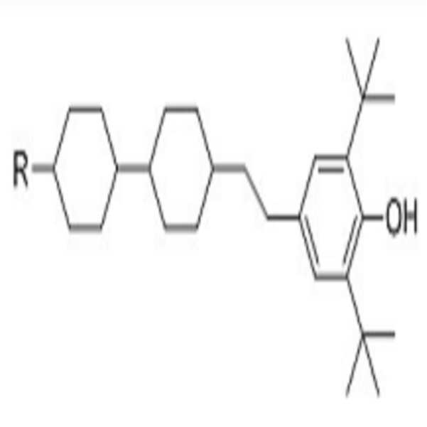
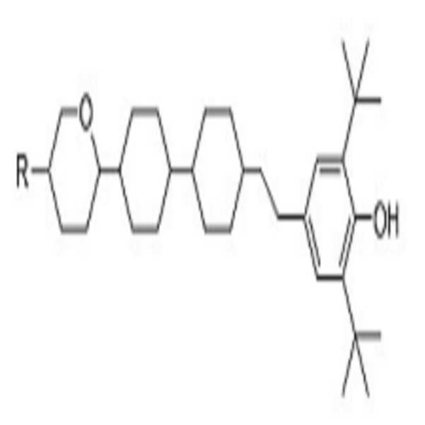
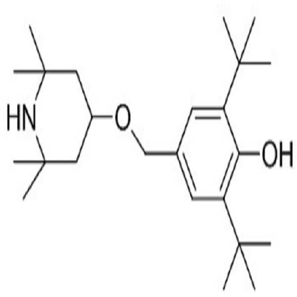
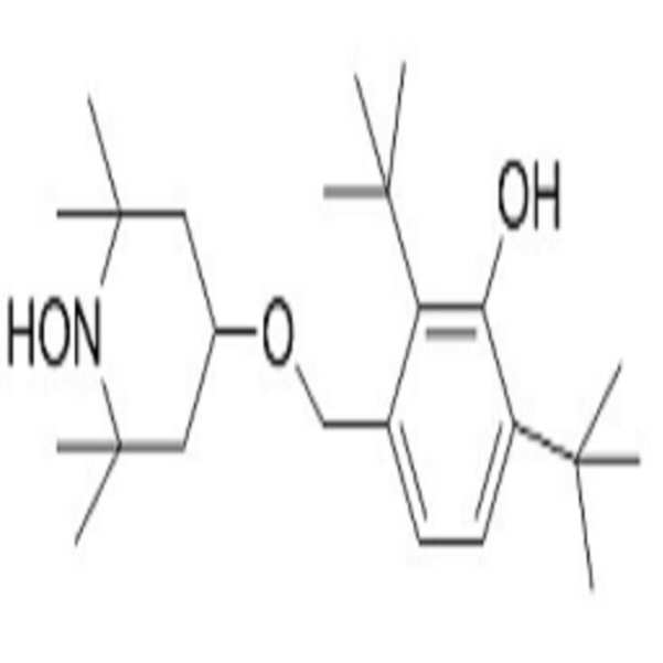
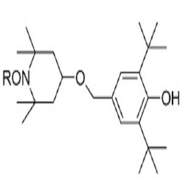
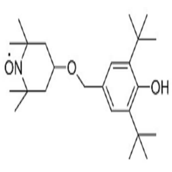
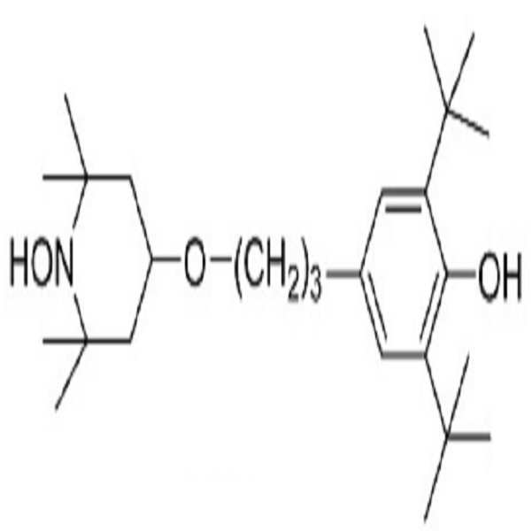
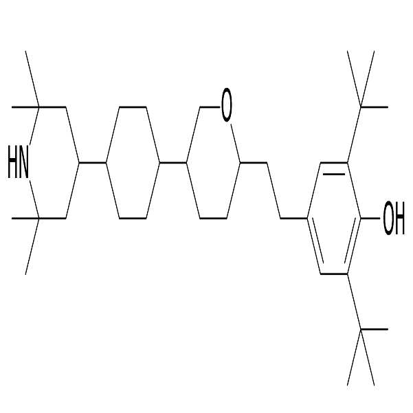
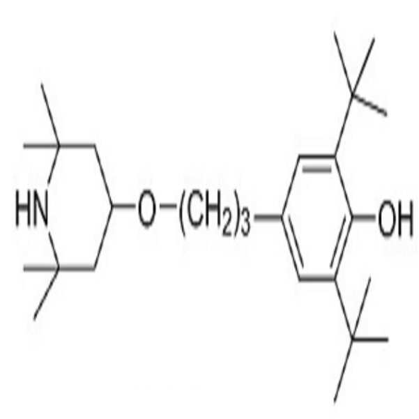
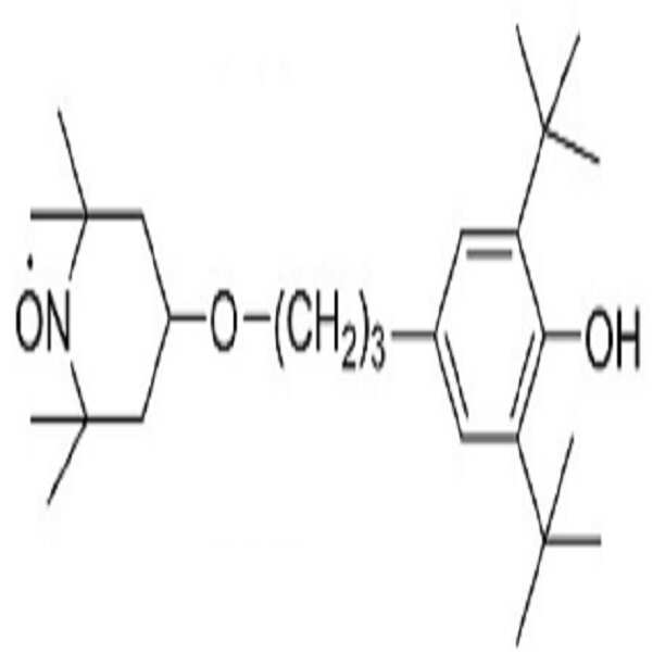
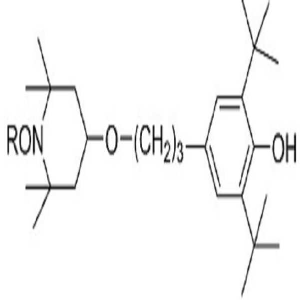
상기 화학식 1로 표현되는 화합물은 전술한 조건을 만족시키는 어떠한 구조도 가능하나, 일례로써 하기 화학식 1-1 내지 화학식 1-28 중 적어도 어느 하나일 수 있다. The compound represented by the formula (1) may have any structure satisfying the above-mentioned conditions. For example, the compound represented by the formula (1) may be at least one of the following formulas (1-1) to (1-28).
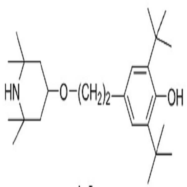


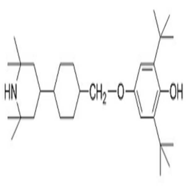


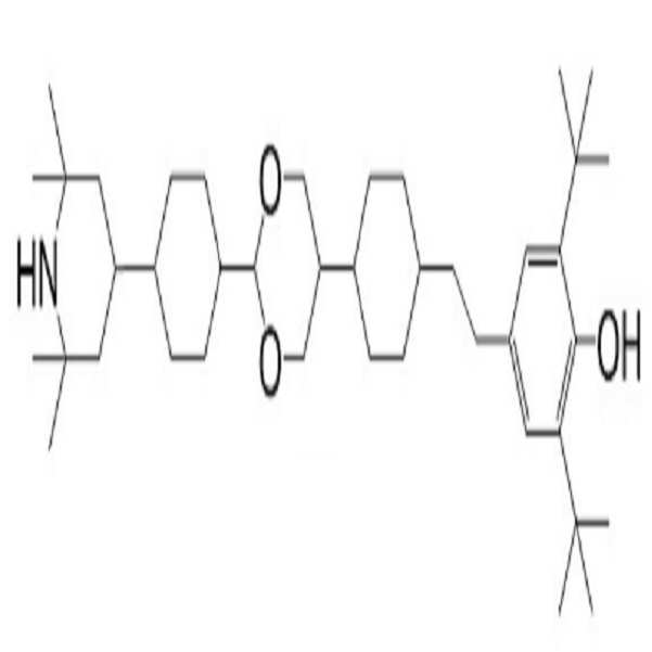
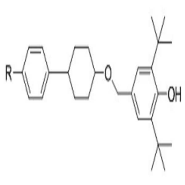
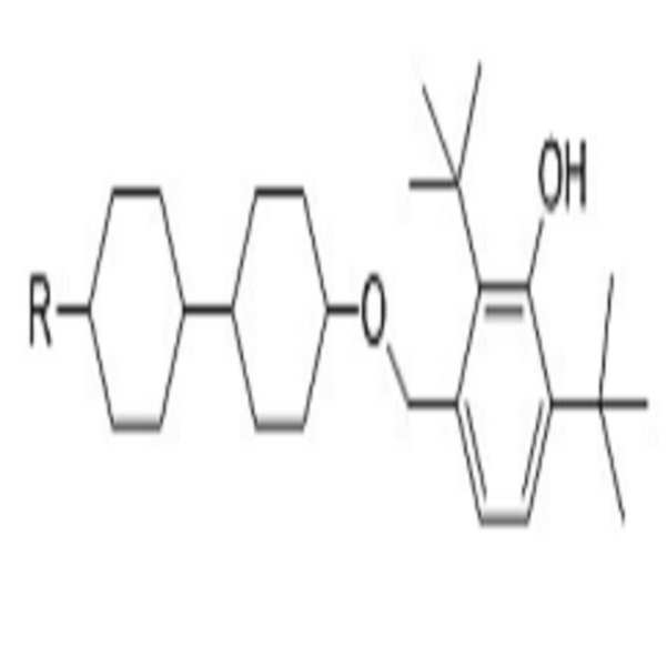
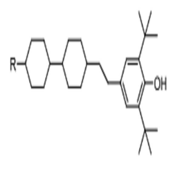
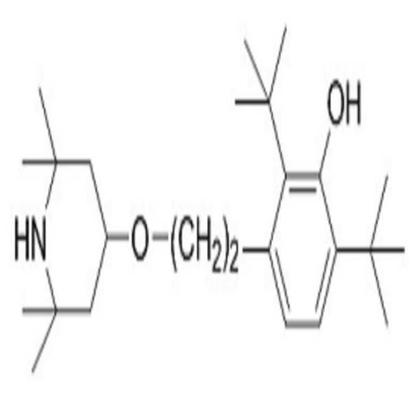
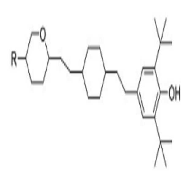
한편, 상기 화학식 2로 표현되는 화합물 역시 전술한 조건을 만족시키는 어떠한 구조도 가능하나, 일례로써 하기 화학식 2-1 내지 화학식 2-16 중 적어도 어느 하나 일 수 있다. The compound represented by Formula 2 may have any of the structures satisfying the above-mentioned conditions. For example, the compound represented by Formula 2 may be any one of the following Formulas 2-1 to 2-16.


화학식 1 및 화학식 2로 표현되는 화합물은 UV 또는 열에 의한 액정 분자의 반응을 억제하는바, 이를 포함하는 액정 조성물의 신뢰성을 향상시킬 수 있다. 또한, 본 실시예에서는 화학식 1 및 화학식 2로 표현되는 화합물을 광안정제로서 배향막에 포함시킴으로써, 액정 조성물에 포함시켜 사용할 때보다 액정의 안정성이 개선될 수 있다.The compounds represented by formulas (1) and (2) inhibit the reaction of liquid crystal molecules by UV or heat, and the reliability of the liquid crystal composition containing the compounds can be improved. In addition, in this embodiment, the stability of the liquid crystal can be improved by incorporating the compound represented by the general formulas (1) and (2) into the alignment layer as a light stabilizer, as compared with the liquid crystal composition.
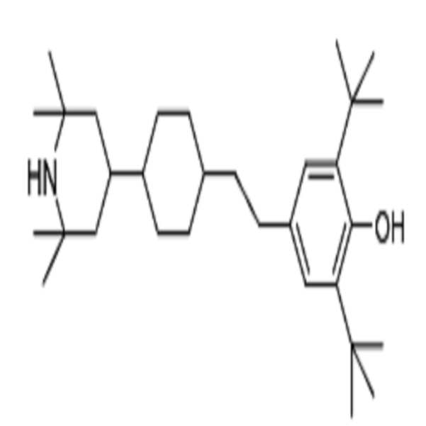
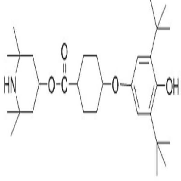
이하에서는 상기 화학식 1로 표현되는 화합물의 일 실시예로서, 하기 화학식 1-1로 표현되는 화합물의 합성에 대해 살펴본다. Hereinafter, the synthesis of the compound represented by the following formula (1-1) will be described as an example of the compound represented by the formula (1).
화학식 1-1은 먼저 하기 반응식 1과 같이, 일정 조건 하에서 화합물 1-A가 합성한다. Compound (1-1) is synthesized first as compound (1-A) under certain conditions as shown in Reaction Scheme 1 below.
[반응식 1][Reaction Scheme 1]
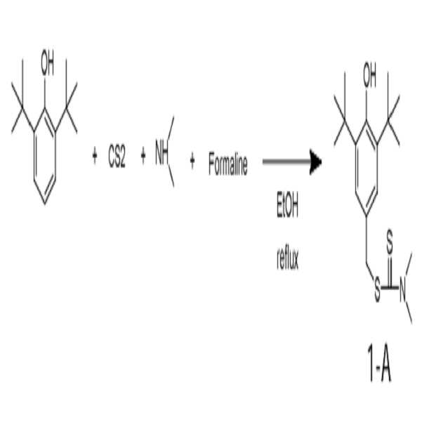
다음, 반응식 1에서 합성된 상기 화합물 1-A를 다시 하기 반응식 2와 같은 조건에서 반응시켜 본 발명의 일 실시예와 같은 화학식 1-1로 표현되는 화합물을 합성한다. Next, the compound 1-A synthesized in Scheme 1 is reacted under the same conditions as Reaction Scheme 2 below to synthesize a compound represented by Formula 1-1 as in one embodiment of the present invention.
[반응식 2][Reaction Scheme 2]

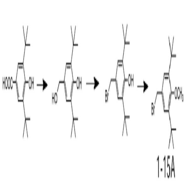
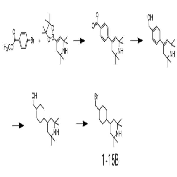
이하에서는 상기 화학식 1로 표현되는 화합물의 일 실시예로서 하기 화학식 1-15로 표현되는 화합물의 합성에 대해 살펴본다. Hereinafter, the synthesis of the compound represented by the following formula 1-15 will be described as an example of the compound represented by the above formula (1).
우선, 하기 반응식 3을 통해 화합물 1-15A를 합성하고, 하기 반응식 4와 같이 화합물 1-15B를 합성한다. First, Compound 1-15A is synthesized through the following
[반응식 3][Reaction Scheme 3]
[반응식 4][Reaction Scheme 4]
이에 따라 합성된 상기 화합물 1-15A 및 화합물 1-15B를 하기 반응식 5를 따라 합성하여 본 발명의 실시에에 따른 상기 화학식 1-15로 표현되는 화합물을 합성할 수 있다. The compound 1-15A and the compound 1-15B thus synthesized can be synthesized according to the following Reaction Scheme 5 to synthesize the compound represented by the above Formula 1-15 according to the practice of the present invention.
[반응식 5][Reaction Scheme 5]

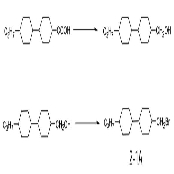
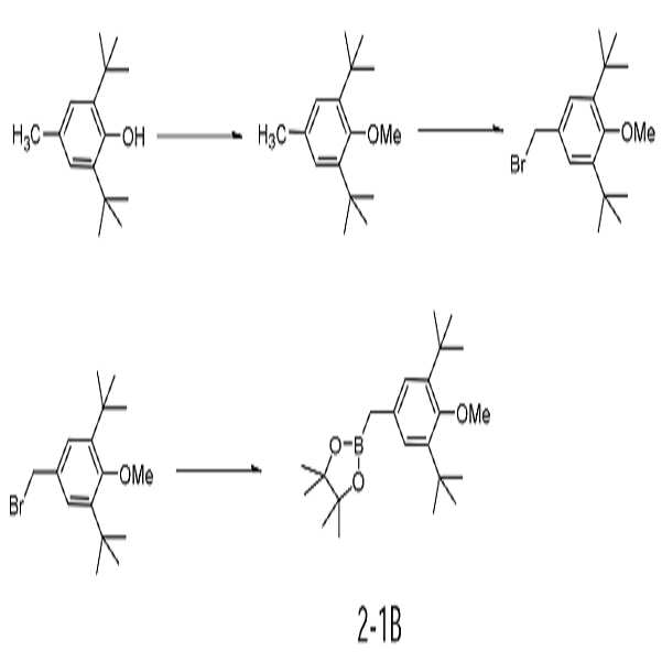
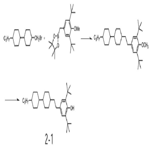
이하에서는 상기 화학식 2로 표현되는 화합물의 일례로써 하기 화학식 2-1로 표현되는 화합물의 합성에 대해 살펴본다. Hereinafter, synthesis of a compound represented by the following formula (2-1) will be described as an example of the compound represented by the formula (2).
우선, 하기 반응식 6을 통해 화합물 2-1A를 합성하고, 하기 반응식 7을 통해 화합물 2-1B를 합성한다. First, Compound 2-1A is synthesized through the following Reaction Scheme 6, and Compound 2-1B is synthesized through the following Reaction Scheme 7.
[반응식 6][Reaction Scheme 6]
[반응식 7][Reaction Scheme 7]
다음 상기 반응식 6 및 반응식 7을 통해 합성된 화합물 2-1A 및 화합물 2-1B를 하기 반응식 8을 통해 합성하여 상기 화학식 2-1로 표현되는 화합물을 합성한다. Compounds 2-1A and 2-1B synthesized through the above Reaction Scheme 6 and Reaction Scheme 7 are synthesized through the following Reaction Scheme 8 to synthesize the compound represented by Formula 2-1.
[반응식 8][Reaction Scheme 8]
이상에서 설명한 반응식 또는 합성 방법은 본 발명의 실시예에 따른 광안정제를 합성하기 위한 것으로서, 이에 제한되지 않으며, 상기 화학식 1 내지 2로 표현되는 화합물을 합성하기 위한 어떠한 방법도 가능하다.The reaction scheme or synthesis method described above is for synthesizing the light stabilizer according to the embodiment of the present invention, but is not limited thereto, and any method for synthesizing the compound represented by the formulas 1 to 2 is possible.
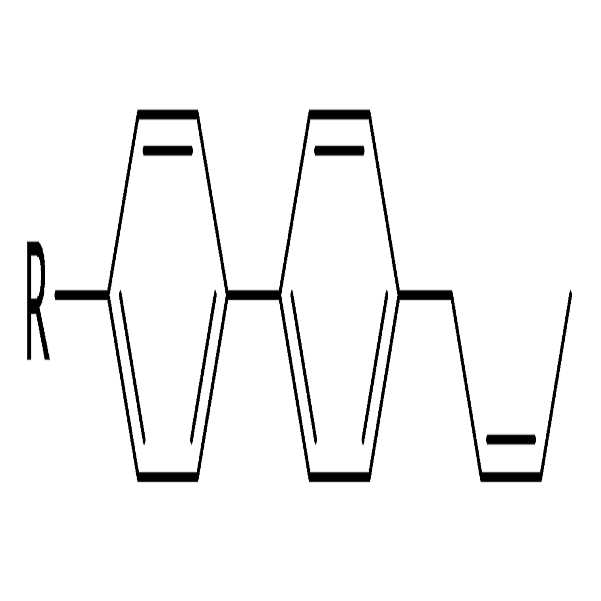
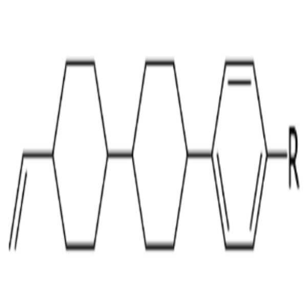
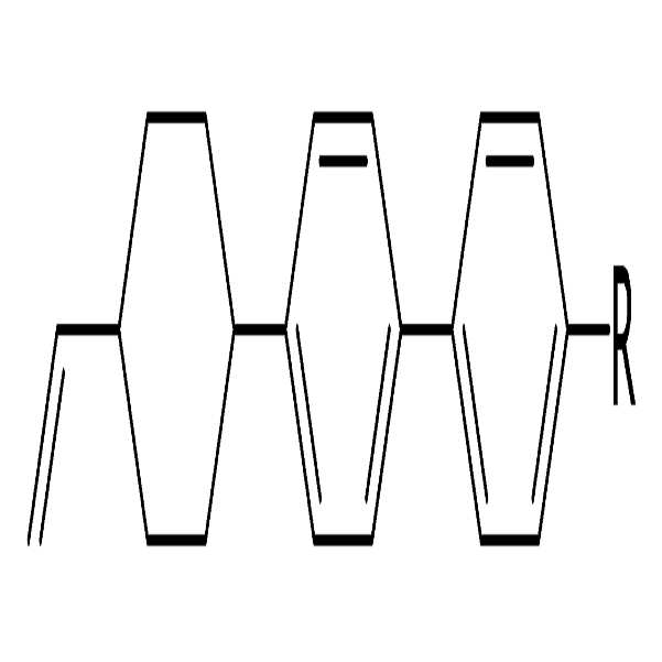
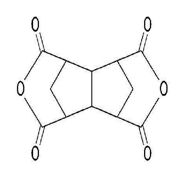
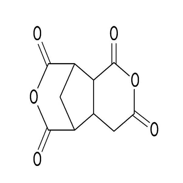
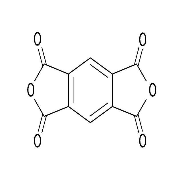
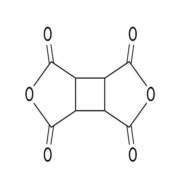
다음으로, 이무수물(dianhydride)계로서 지방고리족 이무수물(alicyclic dianhydride)계 단분자는 하기 화학식 3-1 내지 화학식 3-5 중 어느 하나로 표현되는 단분자일 수 있다. Next, the alicyclic dianhydride monomer as the dianhydride system may be a monomolecule represented by any one of the following formulas (3-1) to (3-5).


디아민(diamine)계로서 방향족 디아민(aromatic diamine)계 단분자는 하기 화학식 4로 표현되는 단분자일 수 있다. The aromatic diamine-based monomolecular diamine system may be a monomolecular monomer represented by the following general formula (4).
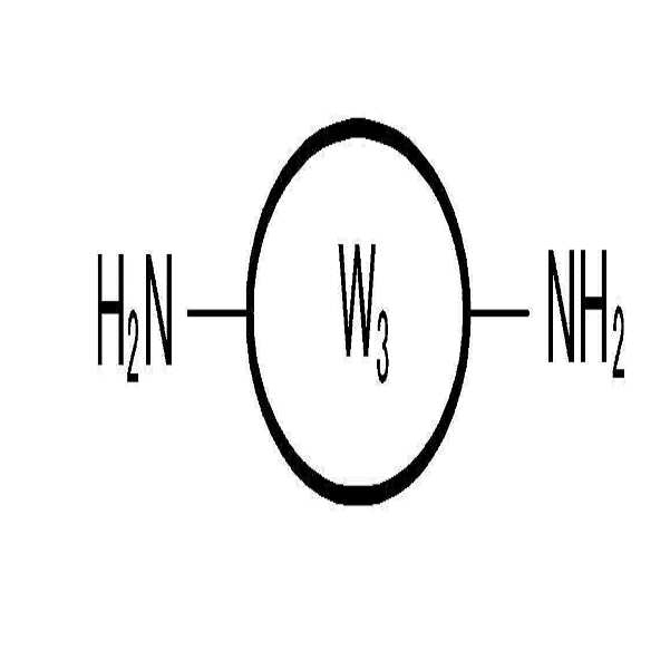
여기서 W3은 하기 화학식 4-1 내지 화학식 4-3 중 어느 하나일 수 있다.Here, W 3 may be any one of the following formulas (4-1) to (4-3).
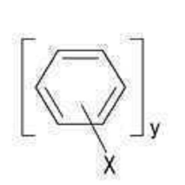
여기서, X는 알킬기이며, y는 1~3의 정수이다.Here, X is an alkyl group and y is an integer of 1 to 3.

디아민(diamine)계로서 지방족 고리 치환 방향족 디아민(aliphatic ring substituted aromatic diamine)계 단분자는 하기 화학식 5로 표현되는 단분자일 수 있다. As a diamine system, an aliphatic ring substituted aromatic diamine-based monomolecule may be a monomolecule represented by the following general formula (5).
여기서, W2는 하기 화학식 5-1과 화학식 5-2 중 어느 하나일 수 있다.Here, W 2 may be any one of the following formulas (5-1) and (5-2).


여기서, x는 1~5의 정수이며, y는 1~10의 정수이다.Here, x is an integer of 1 to 5, and y is an integer of 1 to 10.
디아민(diamine)계로서 광반응성 디아민계 단분자는 반응성 메소겐(RM)을 포함하는 단분자로서, 하기 화학식 6으로 표현되는 단분자일 수 있고, 보다 구체적으로는 화학식 6-1로 표현되는 단분자일 수 있다.As a diamine system, a photoreactive diamine monomolecule may be a monomolecule containing a reactive mesogen (RM), which may be a monomolecule represented by the following formula (6), more specifically, a moiety represented by the formula Lt; / RTI >
여기서, P1은 반응성 메조겐이고, W3는 방향족 고리로서, 위에서 설명한 화학식 4-1 내지 화학식 4-3 중 어느 하나일 수 있다.Here, P 1 is a reactive mesogen, and W 3 is an aromatic ring, which may be any one of the above-described formulas (4-1) to (4-3).
여기서, X는 methylene(CH2), Phenylene (C6H4), Biphenylene (C12H8), Cyclohexylene (C6H8), Bicyclohexylene (C12H16) 및 phenyl-cyclohexylene (C6H4 -C6H8) 중 어느 하나일 수 있고, Y는 methylene(CH2), Ether (O), Ester (O-C=O or O=C-O), Phenylene (C6H4) 및 Cyclohexylene (C6H8) 중 어느 하나일 수 있고, Z는 methyl(CH3)또는 수소(H)이다. 또한, n은 1~10의 한 정수일 수 있다.Wherein, X is methylene (CH 2), Phenylene ( C 6 H 4), Biphenylene (C 12 H 8), Cyclohexylene (C 6 H 8), Bicyclohexylene (C 12 H 16) and phenyl-cyclohexylene (C 6 H 4 -C 6 H 8) may be of any one, Y is a methylene (CH 2), Ether ( O), Ester (OC = O or O = CO), Phenylene (C 6 H 4) and Cyclohexylene (C 6 H 8 ), and Z is methyl (CH 3 ) or hydrogen (H). In addition, n may be an integer of 1 to 10.
디아민(diamine)계로서 알킬화 방향족 다이아민(alkylated aromatic diamine)계 단분자는 하기 화학식 7로 표현되는 단분자일 수 있다. An alkylated aromatic diamine-based monomolecule as a diamine system may be a monomolecule represented by the following general formula (7).
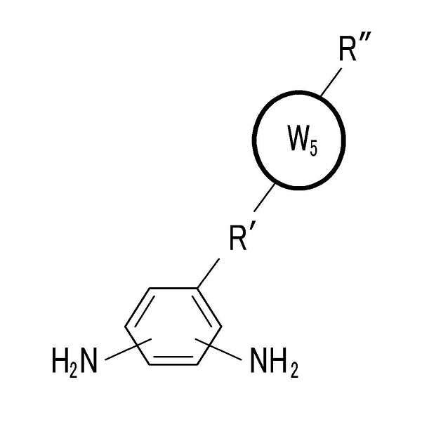
여기서, R'은 -(CH2)n-, -O-(CH2)n-, -(O-C=O 또는 O=C-O)-(CH2)n 중 적어도 하나이며, R"은 -(CH2)n-1-CH3, -O-(CH2)n-1-CH3, -(O-C=O 또는 O=C-O)-(CH2)n-1-CH3이며, n은 1~10이다.Here, R 'is - (CH 2) n -, -O- (CH 2) n -, - (OC = O or O = CO) -, and (CH 2) n at least one of, R "is - (CH 2) n -1-CH 3, -O- (CH 2) n-1 -
또한, W5는 하기 화학식 7-1로 표현될 수 있다.W 5 can be represented by the following formula (7-1).

여기서, x 및 y는 각각 독립적으로 1~3의 정수이다.Here, x and y are each independently an integer of 1 to 3.
다음으로, 하부 표시판(100)과 상부 표시판(200) 사이에는 액정층(3)이 개재되어 있다. 액정층(3)은 복수의 액정 분자(310)를 포함한다. Next, a
본 실시예에서 액정층(3)은 액정 표시 장치에서 응답 속도를 향상시키기 위해 저점도인 알케닐(alkenyl) 싱글을 포함할 수 있다. 알케닐 싱글의 예시로서 하기 화학식 8-1 내지 화학식 8-16 중 적어도 어느 하나를 포함할 수 있으나, 알케닐기를 포함하는 액정 분자라면 이에 한정되지 않는다.In this embodiment, the

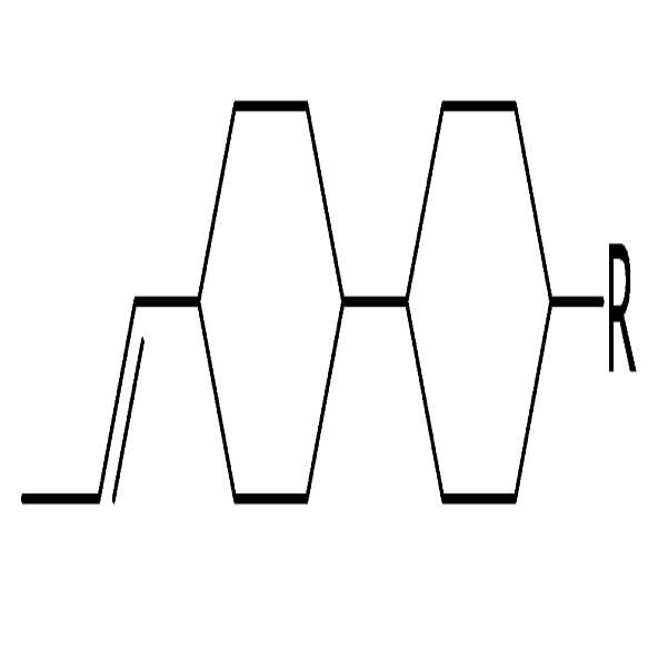


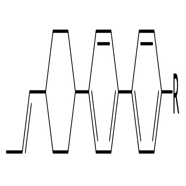
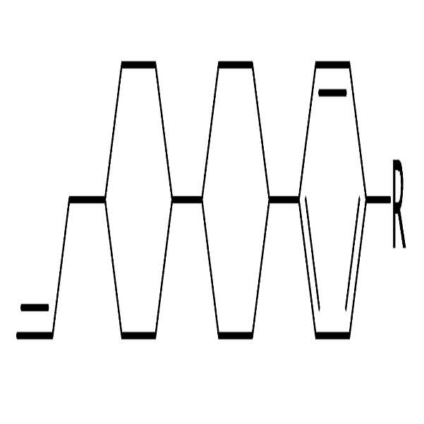


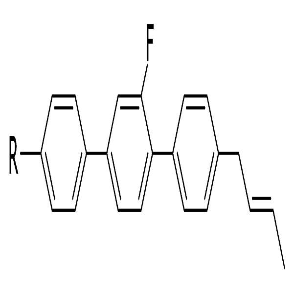


여기서, R은 탄소수 1 내지 5의 알킬기이다.Here, R is an alkyl group having 1 to 5 carbon atoms.
알케닐 싱글은 저점도로서 액정 표시 장치에서 응답 속도를 향상시키는데 있어서 중요한 역할을 하지만, 배향막(11, 21)의 형성 과정에 전계 노광 공정 및 형광 노광 공정을 진행하면 알케닐 부산물 등이 검출되고 선잔상이 발현되는 등 신뢰성이 저하되는 요인이 될 수 있다.The alkenyl single has a low viscosity and plays an important role in improving the response speed in a liquid crystal display. However, when an electric field exposure process and a fluorescent exposure process are performed in the process of forming the
따라서, 본 실시예에서는 배향막(11, 21)에 상기 화학식 1 또는 화학식 2 표현되는 광안정제를 포함하여 알케닐 부산물의 발생을 억제할 수 있고, 표시 장치에서 발생할 수 있는 잔상이 개선될 수 있다.Accordingly, in this embodiment, the occurrence of alkenyl byproducts can be suppressed by including the light stabilizers represented by the above Chemical Formulas 1 or 2 in the
다음, 상부 표시판(200)에 대해서 설명한다.Next, the
상부 표시판(200)에는 투명한 절연 기판(210) 위에 공통 전극(270)이 전면에 형성되어 있다.In the
상부 표시판(200)의 안쪽 면에는 제2 배향막(21)이 형성되어 있으며, 제2 배향막(21)은 수직 배향막일 수 있다. 제2 배향막(21)은 배향 보조제를 광조사하여 형성된 제2 배향 중합체(23a)를 포함한다. 배향 보조제는 반응성 메소겐(Reactive Mesogen)일 수 있으며, 제2 배향막(21)은 앞서 설명한 제1 배향막(11)과 동일한 물질로 형성될 수 있으며 중복되는 설명은 생략한다.A
상부 표시판(200)과 하부 표시판(100) 사이의 간격을 유지하기 위한 간격재(363)가 형성되어 있다.A spacing
하부 표시판(100) 및 상부 표시판(200)의 바깥쪽 면에는 편광자(polarization)(도시하지 않음)가 구비되어 있을 수 있다.Polarizers (not shown) may be provided on the outer surfaces of the
화소 전극(191) 및 공통 전극(270)에 전압이 인가되면, 액정 분자(310)는 화소 전극(191)과 공통 전극(270) 사이에 형성된 전기장에 응답하여 그 장축이 전기장의 방향에 수직한 방향으로 방향을 바꾼다. 액정(310)이 기울어진 정도에 따라 액정층(3)에 입사광의 편광의 변화 정도가 달라지며 이러한 편광의 변화는 편광자에 의하여 투과율 변화로 나타나고 이를 통하여 액정 표시 장치는 영상을 표시한다.When a voltage is applied to the
액정 분자(310)가 기울어지는 방향은 화소 전극(191)의 미세 가지(194)에 의해 결정되며, 액정(310)은 미세 가지(194)의 길이 방향에 평행한 방향으로 기울어진다. 하나의 화소 전극(191)은 미세 가지(194)의 길이 방향이 서로 다른 네 개의 부영역을 포함하므로 액정 분자(310)가 기울어지는 방향은 대략 네 방향이며 액정층(3)에는 액정 분자(310)의 배향 방향이 다른 네 개의 도메인(domain)이 형성된다. 이와 같이 액정이 기울어지는 방향을 다양하게 함으로써 액정 표시 장치의 시야각을 개선할 수 있다.The direction in which the liquid crystal molecules 310 are tilted is determined by the
본 실시예에 따른 액정 표시 장치는 배향 보조제의 중합에 의해 형성된 배향 중합체(13a, 23a)가 액정 분자(310)의 초기 배향 방향인 선경사(pre-tilt)를 제어할 수 있다.The liquid crystal display device according to the present embodiment can control the pre-tilt, which is the initial alignment direction of the liquid crystal molecules 310, by the
이하에서는, 도 4를 참고하여 본 실시예에 따른 배향막을 적용한 액정 표시 장치의 전압 보전율을 측정한 실험 결과에 대해 살펴 본다.Hereinafter, with reference to FIG. 4, the results of measurement of the voltage holding ratio of the liquid crystal display device using the alignment layer according to the present embodiment will be described.
도 4는 본 발명의 일 실시예 및 비교예에 따른 액정 표시 장치의 전압 보전율을 측정한 결과를 나타낸 그래프이다. 실시예 및 비교예에서는 모두 알케닐 싱글을 포함하는 액정층이 적용된 액정 표시 장치를 사용하였다.4 is a graph showing the results of measurement of the voltage holding ratio of the liquid crystal display device according to an embodiment of the present invention and a comparative example. In the examples and comparative examples, a liquid crystal display device to which a liquid crystal layer containing an alkenyl single was applied was used.
도 4의 세로축은 전압 보전율(VHR)을 나타낸다. 또한, 도 4의 가로축은 하기 표 1에 나타난 다양한 광안정제를 각각 포함하는 배향막이 적용된 액정 표시 장치를 나타낸다.The vertical axis in Fig. 4 represents the voltage holding ratio (VHR). The horizontal axis in FIG. 4 represents a liquid crystal display device to which an alignment film containing various light stabilizers shown in Table 1 is applied.


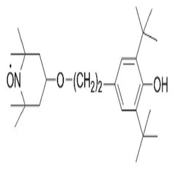
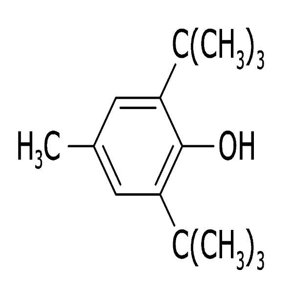
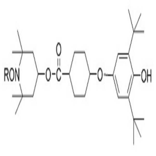
[화학식 1-1]
[Formula 1-1]
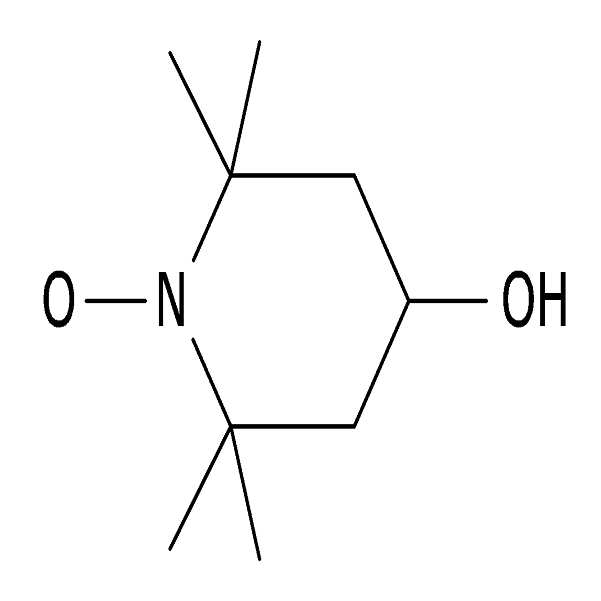
[화학식 9]
[Chemical Formula 9]
[화학식 10]
[Chemical formula 10]
[화학식 11]
(11)
도 4를 참고하면, 비교예 1 내지 비교예 3은 종래 잔상 개선을 위해 사용되어왔던 광안정제로서, 광안정제가 첨가되지 않은 배향막을 사용한 경우에 비해 형광 노광 시간에 따른 전압 보전율이 우수한 것을 확인할 수 있다.Referring to FIG. 4, it was confirmed that Comparative Examples 1 to 3 are superior to conventional photostabilizers for improving afterimage, and exhibit excellent voltage retention according to a fluorescent exposure time, as compared with the case where an alignment film without a light stabilizer is used have.
또한, 본 실시예에 따른 광안정제를 포함하는 실시예 1 및 실시예 2 역시 비교예 1 내지 비교예 3의 기존 광안정제와 유사하거나 우수한 전압 보전율을 가지는 것을 확인할 수 있었다.It was also confirmed that Examples 1 and 2 including the light stabilizer according to the present example had similar or excellent voltage maintenance rates to those of the conventional light stabilizers of Comparative Examples 1 to 3.
따라서, 본 발명의 일 실시예에 따른 광안정제는 알케닐 싱글을 포함하는 액정 표시 장치에서 전압 보전율을 개선할 수 있는 효과가 있음을 확인할 수 있었다.Therefore, it can be seen that the light stabilizer according to one embodiment of the present invention has an effect of improving the voltage maintenance ratio in the liquid crystal display device including the alkenyl single.
이상과 같이 본 발명의 일실시예에 따른 배향막 및 이를 포함하는 액정 표시 장치는 배향막에 신규 광안정제를 포함하고 있어 액정 조성물에서 발생할 수 있는 불순물의 발생을 방지하여 표시 패널에서 발생할 수 있는 잔상 및 신뢰성이 개선될 수 있다.As described above, the alignment layer and the liquid crystal display device including the same according to an embodiment of the present invention include a novel light stabilizer in the alignment layer to prevent the generation of impurities that may occur in the liquid crystal composition, Can be improved.
이상에서 본 발명의 바람직한 실시예에 대하여 상세하게 설명하였지만 본 발명의 권리범위는 이에 한정되는 것은 아니고 다음의 청구범위에서 정의하고 있는 본 발명의 기본 개념을 이용한 당업자의 여러 변형 및 개량 형태 또한 본 발명의 권리범위에 속하는 것이다.While the present invention has been particularly shown and described with reference to exemplary embodiments thereof, it is to be understood that the invention is not limited to the disclosed exemplary embodiments, Of the right.
3: 액정층
11, 21: 배향막
100: 하부 표시판
200: 상부 표시판
121: 게이트선
124a, 124b: 게이트 전극
140: 게이트 절연막
154a, 154b: 반도체층
171a, 171b: 데이터선
173a, 173b: 소스 전극
175a, 175b: 드레인 전극
310: 액정 분자
191: 화소 전극
270: 공통 전극
230: 색필터
13a, 23a: 배향 중합체3:
100: Lower display panel 200: Upper display panel
121:
140:
171a and 171b:
175a, 175b: drain electrode 310: liquid crystal molecule
191: pixel electrode 270: common electrode
230:
Claims (16)

여기서, 상기 X1은 H, O, OR 및 R 중 어느 하나이고, 상기 X2는 O, OCO, OR, RO, NOR, 및 R 중 어느 하나이고, 상기 X3은 O, OCO, OR, RO, NOR 및 R 중 어느 하나이고, 상기 A 및 B는 각각 독립적으로 시클로헥실기, 시클릭에테르기 및 페닐기 중 어느 하나 이상을 포함하고, 상기 R은 탄소수 1 내지 5의 알킬기이며, 상기 m 및 n은 각각 독립적으로 0 내지 2의 자연수이다.An alignment layer comprising at least one of the following photostabilizers represented by the following general formulas (1) and (2)
Here, the X 1 is H, O, and OR, and any one of R, wherein X 2 is O, OCO, OR, RO, NOR, and R is any one of, wherein X 3 is Wherein each of A and B independently represents any one or more of a cyclohexyl group, a cyclic ether group and a phenyl group, and R is an alkylene group having 1 to 5 carbon atoms Alkyl group, and m and n are each independently a natural number of 0 to 2.
상기 화학식 1로 표현되는 광안정제는 하기 화학식 1-1 내지 화학식 1-28로 표현되는 화합물 중 적어도 하나를 포함하는 배향막:


여기서, 상기 R은 탄소수 1 내지 5의 알킬기이다.The method of claim 1,
The light stabilizer represented by Formula 1 may include at least one compound represented by Formula 1-1 to Formula 1-28:
Here, R is an alkyl group having 1 to 5 carbon atoms.
상기 화학식 2로 표현되는 광안정제는 하기 화학식 2-1 내지 화학식 2-16으로 표현되는 화합물 중 적어도 하나를 포함하는 배향막:


여기서, 상기 R은 탄소수 1 내지 5의 알킬기이다.The method of claim 1,
The light stabilizer represented by Formula 2 may include at least one compound represented by Formula 2-1 to Formula 2-16:
Here, R is an alkyl group having 1 to 5 carbon atoms.
상기 배향막은 이무수물(dianhydride)계 단분자를 포함하는 제1 물질, 및
디아민(diamine)계 단분자를 포함하는 제2 물질을 더 포함하는 배향막.The method of claim 1,
Wherein the alignment layer comprises a first material comprising dianhydride monomers,
And a second substance including a diamine-based monomolecule.
상기 광안정제는 상기 디아민계 단분자에 결합되어 있는 배향막.5. The method of claim 4,
Wherein the light stabilizer is bonded to the diamine monomolecule.
상기 제1 물질은 지방고리족 이무수물(alicyclic dianhydride)계 단분자를 포함하고,
상기 제2 물질은 방향족 디아민(aromatic diamine)계 단분자, 지방족 고리 치환 방향족 디아민(aliphatic ring substituted aromatic diamine)계 단분자, 광반응성 디아민계 단분자, 알킬화 방향족 디아민계 단분자 중 적어도 하나 이상을 포함하는 배향막.5. The method of claim 4,
Wherein the first material comprises an alicyclic dianhydride based monomolecular material,
The second material may include at least one of an aromatic diamine-based monomer, an aliphatic ring-substituted aromatic diamine-based monomer, a photoreactive diamine-based monomer, and an alkylated aromatic diamine-based monomer Lt; / RTI >
상기 지방고리족 이무수물계 단분자는 하기 화학식 3-1 내지 화학식 3-5로 표현되는 단분자 중 적어도 하나인 배향막:


Wherein the lipid cyclic dianhydride monomer is at least one of monomers represented by the following formulas (3-1) to (3-5):
상기 제1 기판과 마주보는 제2 기판,
상기 제1 기판 및 상기 제2 기판 중 적어도 어느 하나의 기판 상에 형성된 전기장 생성 전극,
상기 제1 기판 상에 형성된 제1 배향막 및 상기 제2 기판 상에 형성된 제2 배향막, 및
상기 제1 기판과 상기 제2 기판 사이에 개재된 복수의 액정 분자들로 형성된 액정층을 포함하고,
상기 제1 배향막 및 상기 제2 배향막 중 적어도 어느 하나는 하기 화학식 1 및 하기 화학식 2로 표현되는 광안정제 중 적어도 하나를 포함하는 액정 표시 장치:

여기서, 상기 X1은 H, O, OR 및 R 중 어느 하나이고, 상기 X2는 O, OCO, OR, RO, NOR, 및 R 중 어느 하나이고, 상기 X3은 O, OCO, OR, RO, NOR 및 R 중 어느 하나이고, 상기 A 및 B는 각각 독립적으로 시클로헥실기, 시클릭에테르기 및 페닐기 중 어느 하나 이상을 포함하고, 상기 R은 탄소수 1 내지 5의 알킬기이며, 상기 m 및 n은 각각 독립적으로 0 내지 2의 자연수이다.The first substrate,
A second substrate facing the first substrate,
An electric field generating electrode formed on at least one of the first substrate and the second substrate,
A first alignment layer formed on the first substrate and a second alignment layer formed on the second substrate,
And a liquid crystal layer formed of a plurality of liquid crystal molecules interposed between the first substrate and the second substrate,
Wherein at least one of the first alignment layer and the second alignment layer comprises at least one of a light stabilizer represented by the following general formulas (1) and (2)
Here, the X 1 is H, O, and OR, and any one of R, wherein X 2 is O, OCO, OR, RO, NOR, and R is any one of, wherein X 3 is Wherein each of A and B independently represents any one or more of a cyclohexyl group, a cyclic ether group and a phenyl group, and R is an alkylene group having 1 to 5 carbon atoms Alkyl group, and m and n are each independently a natural number of 0 to 2.
상기 액정 분자는 알케닐(alkenyl)기를 포함하는 액정 표시 장치.9. The method of claim 8,
Wherein the liquid crystal molecule comprises an alkenyl group.
상기 알케닐기는 하기 화학식 8-1 내지 화학식 8-16으로 표현되는 화합물 중 적어도 하나를 포함하는 액정 표시 장치:


여기서, R은 탄소수 1 내지 5의 알킬기이다.The method of claim 9,
Wherein the alkenyl group comprises at least one of compounds represented by the following formulas (8-1) to (8-16):
Here, R is an alkyl group having 1 to 5 carbon atoms.
상기 화학식 1로 표현되는 광안정제는 하기 화학식 1-1 내지 화학식 1-28로 표현되는 화합물 중 적어도 하나를 포함하는 액정 표시 장치:


여기서, 상기 R은 탄소수 1 내지 5의 알킬기이다.The method of claim 9,
Wherein the light stabilizer represented by Formula 1 comprises at least one compound represented by Formula 1-1 to Formula 1-28:
Here, R is an alkyl group having 1 to 5 carbon atoms.
상기 화학식 2로 표현되는 광안정제는 하기 화학식 2-1 내지 화학식 2-16으로 표현되는 화합물 중 적어도 하나를 포함하는 액정 표시 장치:


여기서, 상기 R은 탄소수 1 내지 5의 알킬기이다.The method of claim 9,
Wherein the light stabilizer represented by Formula 2 comprises at least one of compounds represented by the following Formulas 2-1 to 2-16:
Here, R is an alkyl group having 1 to 5 carbon atoms.
상기 배향막은 이무수물(dianhydride)계 단분자를 포함하는 제1 물질, 및
디아민(diamine)계 단분자를 포함하는 제2 물질을 더 포함하는 액정 표시 장치.The method of claim 9,
Wherein the alignment layer comprises a first material comprising dianhydride monomers,
And a second material including a diamine-based monomolecule.
상기 광안정제는 상기 디아민계 단분자에 결합되어 있는 액정 표시 장치.The method of claim 13,
Wherein the light stabilizer is bonded to the diamine-based single molecule.
상기 제1 물질은 지방고리족 이무수물(alicyclic dianhydride)계 단분자를 포함하고,
상기 제2 물질은 방향족 디아민(aromatic diamine)계 단분자, 지방족 고리 치환 방향족 디아민(aliphatic ring substituted aromatic diamine)계 단분자, 광반응성 디아민계 단분자, 알킬화 방향족 디아민계 단분자 중 적어도 하나 이상을 포함하는 액정 표시 장치.The method of claim 13,
Wherein the first material comprises an alicyclic dianhydride based monomolecular material,
The second material may include at least one of an aromatic diamine-based monomer, an aliphatic ring-substituted aromatic diamine-based monomer, a photoreactive diamine-based monomer, and an alkylated aromatic diamine-based monomer .
상기 지방고리족 이무수물계 단분자는 하기 화학식 3-1 내지 화학식 3-5로 표현되는 단분자 중 적어도 하나인 액정 표시 장치:


Wherein the fat chain dianhydride monomolecular is at least one of monomers represented by the following formulas (3-1) to (3-5):
Priority Applications (2)
| Application Number | Priority Date | Filing Date | Title |
|---|---|---|---|
| KR1020150109433A KR20170016541A (en) | 2015-08-03 | 2015-08-03 | Alignment layer and liquid crystal display including the same |
| US15/003,825 US20170038642A1 (en) | 2015-08-03 | 2016-01-22 | Alignment layer and liquid crystal display including the same |
Applications Claiming Priority (1)
| Application Number | Priority Date | Filing Date | Title |
|---|---|---|---|
| KR1020150109433A KR20170016541A (en) | 2015-08-03 | 2015-08-03 | Alignment layer and liquid crystal display including the same |
Publications (1)
| Publication Number | Publication Date |
|---|---|
| KR20170016541A true KR20170016541A (en) | 2017-02-14 |
Family
ID=58053862
Family Applications (1)
| Application Number | Title | Priority Date | Filing Date |
|---|---|---|---|
| KR1020150109433A Withdrawn KR20170016541A (en) | 2015-08-03 | 2015-08-03 | Alignment layer and liquid crystal display including the same |
Country Status (2)
| Country | Link |
|---|---|
| US (1) | US20170038642A1 (en) |
| KR (1) | KR20170016541A (en) |
Cited By (2)
| Publication number | Priority date | Publication date | Assignee | Title |
|---|---|---|---|---|
| US10119074B2 (en) | 2016-09-27 | 2018-11-06 | Samsung Display Co., Ltd. | Liquid crystal composition and display device including the same |
| WO2019004709A1 (en) * | 2017-06-29 | 2019-01-03 | 주식회사 엘지화학 | Liquid crystal alignment agent composition, method for producing liquid crystal alignment film using same, and liquid crystal alignment film using same |
Families Citing this family (1)
| Publication number | Priority date | Publication date | Assignee | Title |
|---|---|---|---|---|
| KR102235476B1 (en) | 2018-03-30 | 2021-04-01 | 주식회사 엘지화학 | Liquid crystal alignment composition, method of preparing liquid crystal alignment film, and liquid crystal alignment film using the same |
Family Cites Families (5)
| Publication number | Priority date | Publication date | Assignee | Title |
|---|---|---|---|---|
| DE60114518T2 (en) * | 2000-07-06 | 2006-08-10 | Fuji Photo Film Co. Ltd., Minamiashigara | Liquid crystal composition containing liquid crystal molecules and alignment agents |
| US8349210B2 (en) * | 2008-06-27 | 2013-01-08 | Transitions Optical, Inc. | Mesogenic stabilizers |
| US9081237B2 (en) * | 2010-04-02 | 2015-07-14 | Samsung Display Co., Ltd. | Pixel electrode panel, a liquid crystal display panel assembly and methods for manufacturing the same |
| US20130271713A1 (en) * | 2010-10-14 | 2013-10-17 | Sharp Kabushiki Kaisha | Liquid crystal display device and method for manufacturing liquid crystal display device |
| KR102416574B1 (en) * | 2015-08-18 | 2022-07-08 | 삼성디스플레이 주식회사 | Curved liquid crystal display and method for manufacturing the same |
-
2015
- 2015-08-03 KR KR1020150109433A patent/KR20170016541A/en not_active Withdrawn
-
2016
- 2016-01-22 US US15/003,825 patent/US20170038642A1/en not_active Abandoned
Cited By (3)
| Publication number | Priority date | Publication date | Assignee | Title |
|---|---|---|---|---|
| US10119074B2 (en) | 2016-09-27 | 2018-11-06 | Samsung Display Co., Ltd. | Liquid crystal composition and display device including the same |
| WO2019004709A1 (en) * | 2017-06-29 | 2019-01-03 | 주식회사 엘지화학 | Liquid crystal alignment agent composition, method for producing liquid crystal alignment film using same, and liquid crystal alignment film using same |
| US11142697B2 (en) | 2017-06-29 | 2021-10-12 | Lg Chem, Ltd. | Liquid crystal aligning agent composition, method for producing liquid crystal alignment film using same, and liquid crystal alignment film using same |
Also Published As
| Publication number | Publication date |
|---|---|
| US20170038642A1 (en) | 2017-02-09 |
Similar Documents
| Publication | Publication Date | Title |
|---|---|---|
| KR101644046B1 (en) | Liquid crystal device | |
| JP5503896B2 (en) | Liquid crystal display | |
| CN105938277B (en) | Curved liquid crystal display and method of making a curved liquid crystal display | |
| KR20110021587A (en) | Liquid Crystal Display and Manufacturing Method Thereof | |
| CN106094349B (en) | LCD Monitor | |
| CN113785239B (en) | Liquid crystal display device having a light shielding layer | |
| KR20150030526A (en) | Liquid crystal display device | |
| US20170052412A1 (en) | Curved liquid crystal display and method of manufacturing the same | |
| EP3053990B1 (en) | Liquid crystal composition and liquid crystal display including the same | |
| KR20170016541A (en) | Alignment layer and liquid crystal display including the same | |
| EP3042923B1 (en) | Liquid crystal display | |
| KR102272215B1 (en) | Liquid crystal composition, liquid crystal display including the same, and manufacturing method thereof | |
| CN107868666B (en) | Liquid crystal composition and display device including the same | |
| KR20170008338A (en) | Liquid crystal composition and liquid crystal display including the same | |
| KR20170010242A (en) | Liquid crystal display | |
| JP2016057620A (en) | Photo-alignment agent, photo-alignment film, liquid crystal display device, and production method thereof | |
| KR102298368B1 (en) | Photo alignment agent, photo alignment layer, liquid crystal display device and method of manufacturing the same | |
| KR20150109008A (en) | Liquid crystal composition and liquid crystal display comprising the same | |
| TW201634676A (en) | Liquid crystal display | |
| EP3070517B1 (en) | Liquid crystal display device having polymer alignment layers with side chains including ion-attracting groups | |
| KR20160052898A (en) | Liquid crystal compositon and liquid crystal display device including the same | |
| EP3076233B1 (en) | Polymeric alignment layers in a curved vertically-aligned liquid crystal display | |
| JP5892330B2 (en) | Liquid crystal alignment agent | |
| KR102388345B1 (en) | Liquid crystal composition and liquid crystal display device comprising the same | |
| KR20170015800A (en) | Liquid crystal composition and liquid crystal display including the same |
Legal Events
| Date | Code | Title | Description |
|---|---|---|---|
| PA0109 | Patent application |
Patent event code: PA01091R01D Comment text: Patent Application Patent event date: 20150803 |
|
| PG1501 | Laying open of application | ||
| PC1203 | Withdrawal of no request for examination |