KR20160090588A - Electronic paper display device - Google Patents
Electronic paper display device Download PDFInfo
- Publication number
- KR20160090588A KR20160090588A KR1020150010567A KR20150010567A KR20160090588A KR 20160090588 A KR20160090588 A KR 20160090588A KR 1020150010567 A KR1020150010567 A KR 1020150010567A KR 20150010567 A KR20150010567 A KR 20150010567A KR 20160090588 A KR20160090588 A KR 20160090588A
- Authority
- KR
- South Korea
- Prior art keywords
- electrode
- electronic paper
- piezoelectric substrate
- display device
- particles
- Prior art date
- Legal status (The legal status is an assumption and is not a legal conclusion. Google has not performed a legal analysis and makes no representation as to the accuracy of the status listed.)
- Withdrawn
Links
- 239000000758 substrate Substances 0.000 claims abstract description 45
- 238000000034 method Methods 0.000 claims description 19
- 239000000463 material Substances 0.000 claims description 11
- 239000003094 microcapsule Substances 0.000 claims description 9
- 239000002131 composite material Substances 0.000 claims description 8
- 239000000835 fiber Substances 0.000 claims description 8
- 239000002033 PVDF binder Substances 0.000 claims description 4
- 229920002981 polyvinylidene fluoride Polymers 0.000 claims description 4
- 239000011241 protective layer Substances 0.000 claims description 4
- 239000002245 particle Substances 0.000 description 25
- -1 polysulfonamide Polymers 0.000 description 13
- 230000002776 aggregation Effects 0.000 description 9
- 238000004220 aggregation Methods 0.000 description 7
- 239000006185 dispersion Substances 0.000 description 6
- 239000007788 liquid Substances 0.000 description 6
- 238000001962 electrophoresis Methods 0.000 description 5
- 239000012780 transparent material Substances 0.000 description 5
- NRCMAYZCPIVABH-UHFFFAOYSA-N Quinacridone Chemical compound N1C2=CC=CC=C2C(=O)C2=C1C=C1C(=O)C3=CC=CC=C3NC1=C2 NRCMAYZCPIVABH-UHFFFAOYSA-N 0.000 description 4
- 229910052793 cadmium Inorganic materials 0.000 description 4
- BDOSMKKIYDKNTQ-UHFFFAOYSA-N cadmium atom Chemical compound [Cd] BDOSMKKIYDKNTQ-UHFFFAOYSA-N 0.000 description 4
- 239000003086 colorant Substances 0.000 description 4
- 229920002635 polyurethane Polymers 0.000 description 4
- 239000004814 polyurethane Substances 0.000 description 4
- 238000002834 transmittance Methods 0.000 description 4
- UHOVQNZJYSORNB-UHFFFAOYSA-N Benzene Chemical compound C1=CC=CC=C1 UHOVQNZJYSORNB-UHFFFAOYSA-N 0.000 description 3
- XEKOWRVHYACXOJ-UHFFFAOYSA-N Ethyl acetate Chemical compound CCOC(C)=O XEKOWRVHYACXOJ-UHFFFAOYSA-N 0.000 description 3
- GWEVSGVZZGPLCZ-UHFFFAOYSA-N Titan oxide Chemical compound O=[Ti]=O GWEVSGVZZGPLCZ-UHFFFAOYSA-N 0.000 description 3
- YXFVVABEGXRONW-UHFFFAOYSA-N Toluene Chemical compound CC1=CC=CC=C1 YXFVVABEGXRONW-UHFFFAOYSA-N 0.000 description 3
- 239000002775 capsule Substances 0.000 description 3
- 229910017052 cobalt Inorganic materials 0.000 description 3
- 239000010941 cobalt Substances 0.000 description 3
- GUTLYIVDDKVIGB-UHFFFAOYSA-N cobalt atom Chemical compound [Co] GUTLYIVDDKVIGB-UHFFFAOYSA-N 0.000 description 3
- 230000005684 electric field Effects 0.000 description 3
- 239000008393 encapsulating agent Substances 0.000 description 3
- VLKZOEOYAKHREP-UHFFFAOYSA-N n-Hexane Chemical compound CCCCCC VLKZOEOYAKHREP-UHFFFAOYSA-N 0.000 description 3
- NXQMCAOPTPLPRL-UHFFFAOYSA-N 2-(2-benzoyloxyethoxy)ethyl benzoate Chemical compound C=1C=CC=CC=1C(=O)OCCOCCOC(=O)C1=CC=CC=C1 NXQMCAOPTPLPRL-UHFFFAOYSA-N 0.000 description 2
- VTYYLEPIZMXCLO-UHFFFAOYSA-L Calcium carbonate Chemical compound [Ca+2].[O-]C([O-])=O VTYYLEPIZMXCLO-UHFFFAOYSA-L 0.000 description 2
- HEDRZPFGACZZDS-UHFFFAOYSA-N Chloroform Chemical compound ClC(Cl)Cl HEDRZPFGACZZDS-UHFFFAOYSA-N 0.000 description 2
- 229910000684 Cobalt-chrome Inorganic materials 0.000 description 2
- RYGMFSIKBFXOCR-UHFFFAOYSA-N Copper Chemical compound [Cu] RYGMFSIKBFXOCR-UHFFFAOYSA-N 0.000 description 2
- VOWAEIGWURALJQ-UHFFFAOYSA-N Dicyclohexyl phthalate Chemical compound C=1C=CC=C(C(=O)OC2CCCCC2)C=1C(=O)OC1CCCCC1 VOWAEIGWURALJQ-UHFFFAOYSA-N 0.000 description 2
- YNQLUTRBYVCPMQ-UHFFFAOYSA-N Ethylbenzene Chemical compound CCC1=CC=CC=C1 YNQLUTRBYVCPMQ-UHFFFAOYSA-N 0.000 description 2
- PXHVJJICTQNCMI-UHFFFAOYSA-N Nickel Chemical compound [Ni] PXHVJJICTQNCMI-UHFFFAOYSA-N 0.000 description 2
- JUJWROOIHBZHMG-UHFFFAOYSA-N Pyridine Chemical compound C1=CC=NC=C1 JUJWROOIHBZHMG-UHFFFAOYSA-N 0.000 description 2
- VYPSYNLAJGMNEJ-UHFFFAOYSA-N Silicium dioxide Chemical compound O=[Si]=O VYPSYNLAJGMNEJ-UHFFFAOYSA-N 0.000 description 2
- RTAQQCXQSZGOHL-UHFFFAOYSA-N Titanium Chemical compound [Ti] RTAQQCXQSZGOHL-UHFFFAOYSA-N 0.000 description 2
- XLOMVQKBTHCTTD-UHFFFAOYSA-N Zinc monoxide Chemical compound [Zn]=O XLOMVQKBTHCTTD-UHFFFAOYSA-N 0.000 description 2
- 239000002253 acid Substances 0.000 description 2
- 238000005054 agglomeration Methods 0.000 description 2
- TZCXTZWJZNENPQ-UHFFFAOYSA-L barium sulfate Chemical compound [Ba+2].[O-]S([O-])(=O)=O TZCXTZWJZNENPQ-UHFFFAOYSA-L 0.000 description 2
- 230000008901 benefit Effects 0.000 description 2
- 239000010952 cobalt-chrome Substances 0.000 description 2
- 229910052802 copper Inorganic materials 0.000 description 2
- 239000010949 copper Substances 0.000 description 2
- QDOXWKRWXJOMAK-UHFFFAOYSA-N dichromium trioxide Chemical compound O=[Cr]O[Cr]=O QDOXWKRWXJOMAK-UHFFFAOYSA-N 0.000 description 2
- 239000004205 dimethyl polysiloxane Substances 0.000 description 2
- 239000007772 electrode material Substances 0.000 description 2
- 239000012530 fluid Substances 0.000 description 2
- 229930195733 hydrocarbon Natural products 0.000 description 2
- 150000002430 hydrocarbons Chemical class 0.000 description 2
- 239000001023 inorganic pigment Substances 0.000 description 2
- 239000010410 layer Substances 0.000 description 2
- 239000002923 metal particle Substances 0.000 description 2
- PYUYQYBDJFMFTH-WMMMYUQOSA-N naphthol red Chemical compound CCOC1=CC=CC=C1NC(=O)C(C1=O)=CC2=CC=CC=C2\C1=N\NC1=CC=C(C(N)=O)C=C1 PYUYQYBDJFMFTH-WMMMYUQOSA-N 0.000 description 2
- 239000012860 organic pigment Substances 0.000 description 2
- 238000005192 partition Methods 0.000 description 2
- XNGIFLGASWRNHJ-UHFFFAOYSA-N phthalic acid Chemical compound OC(=O)C1=CC=CC=C1C(O)=O XNGIFLGASWRNHJ-UHFFFAOYSA-N 0.000 description 2
- 239000000049 pigment Substances 0.000 description 2
- 229920000435 poly(dimethylsiloxane) Polymers 0.000 description 2
- 229920003229 poly(methyl methacrylate) Polymers 0.000 description 2
- 229920000515 polycarbonate Polymers 0.000 description 2
- 239000004417 polycarbonate Substances 0.000 description 2
- 229920000139 polyethylene terephthalate Polymers 0.000 description 2
- 239000005020 polyethylene terephthalate Substances 0.000 description 2
- 239000004926 polymethyl methacrylate Substances 0.000 description 2
- 239000010936 titanium Substances 0.000 description 2
- 229910052719 titanium Inorganic materials 0.000 description 2
- 229910000859 α-Fe Inorganic materials 0.000 description 2
- IIPCXIGUIPAGQB-SEYXRHQNSA-N (z)-4-dodecoxy-4-oxobut-2-enoic acid Chemical compound CCCCCCCCCCCCOC(=O)\C=C/C(O)=O IIPCXIGUIPAGQB-SEYXRHQNSA-N 0.000 description 1
- IAUKWGFWINVWKS-UHFFFAOYSA-N 1,2-di(propan-2-yl)naphthalene Chemical compound C1=CC=CC2=C(C(C)C)C(C(C)C)=CC=C21 IAUKWGFWINVWKS-UHFFFAOYSA-N 0.000 description 1
- PKQYSCBUFZOAPE-UHFFFAOYSA-N 1,2-dibenzyl-3-methylbenzene Chemical compound C=1C=CC=CC=1CC=1C(C)=CC=CC=1CC1=CC=CC=C1 PKQYSCBUFZOAPE-UHFFFAOYSA-N 0.000 description 1
- YJTKZCDBKVTVBY-UHFFFAOYSA-N 1,3-Diphenylbenzene Chemical group C1=CC=CC=C1C1=CC=CC(C=2C=CC=CC=2)=C1 YJTKZCDBKVTVBY-UHFFFAOYSA-N 0.000 description 1
- VYOWNYLBHHBVDR-UHFFFAOYSA-N 1-(3-methylbutyl)-2-phenylbenzene Chemical group CC(C)CCC1=CC=CC=C1C1=CC=CC=C1 VYOWNYLBHHBVDR-UHFFFAOYSA-N 0.000 description 1
- KTHUKEZOIFYPEH-UHFFFAOYSA-N 1-benzylnaphthalene Chemical class C=1C=CC2=CC=CC=C2C=1CC1=CC=CC=C1 KTHUKEZOIFYPEH-UHFFFAOYSA-N 0.000 description 1
- BJCIHMAOTRVTJI-UHFFFAOYSA-N 2-butoxy-n,n-dibutyl-5-(2,4,4-trimethylpentan-2-yl)aniline Chemical compound CCCCOC1=CC=C(C(C)(C)CC(C)(C)C)C=C1N(CCCC)CCCC BJCIHMAOTRVTJI-UHFFFAOYSA-N 0.000 description 1
- SBUYFICWQNHBCM-UHFFFAOYSA-N 4-Ethyl-o-xylene Chemical compound CCC1=CC=C(C)C(C)=C1 SBUYFICWQNHBCM-UHFFFAOYSA-N 0.000 description 1
- DWDURZSYQTXVIN-UHFFFAOYSA-N 4-[(4-aminophenyl)-(4-methyliminocyclohexa-2,5-dien-1-ylidene)methyl]aniline Chemical compound C1=CC(=NC)C=CC1=C(C=1C=CC(N)=CC=1)C1=CC=C(N)C=C1 DWDURZSYQTXVIN-UHFFFAOYSA-N 0.000 description 1
- OMIHGPLIXGGMJB-UHFFFAOYSA-N 7-oxabicyclo[4.1.0]hepta-1,3,5-triene Chemical class C1=CC=C2OC2=C1 OMIHGPLIXGGMJB-UHFFFAOYSA-N 0.000 description 1
- CGLVZFOCZLHKOH-UHFFFAOYSA-N 8,18-dichloro-5,15-diethyl-5,15-dihydrodiindolo(3,2-b:3',2'-m)triphenodioxazine Chemical compound CCN1C2=CC=CC=C2C2=C1C=C1OC3=C(Cl)C4=NC(C=C5C6=CC=CC=C6N(C5=C5)CC)=C5OC4=C(Cl)C3=NC1=C2 CGLVZFOCZLHKOH-UHFFFAOYSA-N 0.000 description 1
- NIXOWILDQLNWCW-UHFFFAOYSA-M Acrylate Chemical compound [O-]C(=O)C=C NIXOWILDQLNWCW-UHFFFAOYSA-M 0.000 description 1
- 239000005995 Aluminium silicate Substances 0.000 description 1
- REEFSLKDEDEWAO-UHFFFAOYSA-N Chloraniformethan Chemical compound ClC1=CC=C(NC(NC=O)C(Cl)(Cl)Cl)C=C1Cl REEFSLKDEDEWAO-UHFFFAOYSA-N 0.000 description 1
- 239000004986 Cholesteric liquid crystals (ChLC) Substances 0.000 description 1
- XDTMQSROBMDMFD-UHFFFAOYSA-N Cyclohexane Chemical compound C1CCCCC1 XDTMQSROBMDMFD-UHFFFAOYSA-N 0.000 description 1
- PYGXAGIECVVIOZ-UHFFFAOYSA-N Dibutyl decanedioate Chemical compound CCCCOC(=O)CCCCCCCCC(=O)OCCCC PYGXAGIECVVIOZ-UHFFFAOYSA-N 0.000 description 1
- 108010010803 Gelatin Proteins 0.000 description 1
- UQSXHKLRYXJYBZ-UHFFFAOYSA-N Iron oxide Chemical compound [Fe]=O UQSXHKLRYXJYBZ-UHFFFAOYSA-N 0.000 description 1
- PWHULOQIROXLJO-UHFFFAOYSA-N Manganese Chemical compound [Mn] PWHULOQIROXLJO-UHFFFAOYSA-N 0.000 description 1
- 229920000877 Melamine resin Polymers 0.000 description 1
- CTQNGGLPUBDAKN-UHFFFAOYSA-N O-Xylene Chemical compound CC1=CC=CC=C1C CTQNGGLPUBDAKN-UHFFFAOYSA-N 0.000 description 1
- CYTYCFOTNPOANT-UHFFFAOYSA-N Perchloroethylene Chemical group ClC(Cl)=C(Cl)Cl CYTYCFOTNPOANT-UHFFFAOYSA-N 0.000 description 1
- 241001310793 Podium Species 0.000 description 1
- 229920012266 Poly(ether sulfone) PES Polymers 0.000 description 1
- 239000004952 Polyamide Substances 0.000 description 1
- 229920002396 Polyurea Polymers 0.000 description 1
- ATJFFYVFTNAWJD-UHFFFAOYSA-N Tin Chemical compound [Sn] ATJFFYVFTNAWJD-UHFFFAOYSA-N 0.000 description 1
- FNYLWPVRPXGIIP-UHFFFAOYSA-N Triamterene Chemical compound NC1=NC2=NC(N)=NC(N)=C2N=C1C1=CC=CC=C1 FNYLWPVRPXGIIP-UHFFFAOYSA-N 0.000 description 1
- XSTXAVWGXDQKEL-UHFFFAOYSA-N Trichloroethylene Chemical group ClC=C(Cl)Cl XSTXAVWGXDQKEL-UHFFFAOYSA-N 0.000 description 1
- WGLPBDUCMAPZCE-UHFFFAOYSA-N Trioxochromium Chemical compound O=[Cr](=O)=O WGLPBDUCMAPZCE-UHFFFAOYSA-N 0.000 description 1
- 229920001807 Urea-formaldehyde Polymers 0.000 description 1
- XTXRWKRVRITETP-UHFFFAOYSA-N Vinyl acetate Chemical compound CC(=O)OC=C XTXRWKRVRITETP-UHFFFAOYSA-N 0.000 description 1
- 229910001037 White iron Inorganic materials 0.000 description 1
- HCHKCACWOHOZIP-UHFFFAOYSA-N Zinc Chemical compound [Zn] HCHKCACWOHOZIP-UHFFFAOYSA-N 0.000 description 1
- 125000005396 acrylic acid ester group Chemical group 0.000 description 1
- 230000004931 aggregating effect Effects 0.000 description 1
- GZCGUPFRVQAUEE-SLPGGIOYSA-N aldehydo-D-glucose Chemical compound OC[C@@H](O)[C@@H](O)[C@H](O)[C@@H](O)C=O GZCGUPFRVQAUEE-SLPGGIOYSA-N 0.000 description 1
- 150000001338 aliphatic hydrocarbons Chemical class 0.000 description 1
- 150000004997 alkyl benzene derivatives Chemical class 0.000 description 1
- 229910052782 aluminium Inorganic materials 0.000 description 1
- XAGFODPZIPBFFR-UHFFFAOYSA-N aluminium Chemical compound [Al] XAGFODPZIPBFFR-UHFFFAOYSA-N 0.000 description 1
- PNEYBMLMFCGWSK-UHFFFAOYSA-N aluminium oxide Inorganic materials [O-2].[O-2].[O-2].[Al+3].[Al+3] PNEYBMLMFCGWSK-UHFFFAOYSA-N 0.000 description 1
- 235000012211 aluminium silicate Nutrition 0.000 description 1
- 229910000410 antimony oxide Inorganic materials 0.000 description 1
- 150000004945 aromatic hydrocarbons Chemical class 0.000 description 1
- XBYNNYGGLWJASC-UHFFFAOYSA-N barium titanium Chemical compound [Ti].[Ba] XBYNNYGGLWJASC-UHFFFAOYSA-N 0.000 description 1
- 229940067573 brown iron oxide Drugs 0.000 description 1
- CJOBVZJTOIVNNF-UHFFFAOYSA-N cadmium sulfide Chemical compound [Cd]=S CJOBVZJTOIVNNF-UHFFFAOYSA-N 0.000 description 1
- 229910000019 calcium carbonate Inorganic materials 0.000 description 1
- 239000000378 calcium silicate Substances 0.000 description 1
- 229910052918 calcium silicate Inorganic materials 0.000 description 1
- OYACROKNLOSFPA-UHFFFAOYSA-N calcium;dioxido(oxo)silane Chemical compound [Ca+2].[O-][Si]([O-])=O OYACROKNLOSFPA-UHFFFAOYSA-N 0.000 description 1
- 239000006229 carbon black Substances 0.000 description 1
- 235000012730 carminic acid Nutrition 0.000 description 1
- 230000008859 change Effects 0.000 description 1
- 239000002801 charged material Substances 0.000 description 1
- HBHZKFOUIUMKHV-UHFFFAOYSA-N chembl1982121 Chemical compound OC1=CC=C2C=CC=CC2=C1N=NC1=CC=C([N+]([O-])=O)C=C1[N+]([O-])=O HBHZKFOUIUMKHV-UHFFFAOYSA-N 0.000 description 1
- ZLFVRXUOSPRRKQ-UHFFFAOYSA-N chembl2138372 Chemical compound [O-][N+](=O)C1=CC(C)=CC=C1N=NC1=C(O)C=CC2=CC=CC=C12 ZLFVRXUOSPRRKQ-UHFFFAOYSA-N 0.000 description 1
- 239000003795 chemical substances by application Substances 0.000 description 1
- SXKJCXWNWBRZGB-UHFFFAOYSA-N chromium copper manganese Chemical compound [Mn][Cr][Cu] SXKJCXWNWBRZGB-UHFFFAOYSA-N 0.000 description 1
- 229910000423 chromium oxide Inorganic materials 0.000 description 1
- 229910000152 cobalt phosphate Inorganic materials 0.000 description 1
- NNSIWZRTNZEWMS-UHFFFAOYSA-N cobalt titanium Chemical compound [Ti].[Co] NNSIWZRTNZEWMS-UHFFFAOYSA-N 0.000 description 1
- 150000001875 compounds Chemical class 0.000 description 1
- 229920001940 conductive polymer Polymers 0.000 description 1
- 239000004020 conductor Substances 0.000 description 1
- 238000011109 contamination Methods 0.000 description 1
- XCJYREBRNVKWGJ-UHFFFAOYSA-N copper(II) phthalocyanine Chemical compound [Cu+2].C12=CC=CC=C2C(N=C2[N-]C(C3=CC=CC=C32)=N2)=NC1=NC([C]1C=CC=CC1=1)=NC=1N=C1[C]3C=CC=CC3=C2[N-]1 XCJYREBRNVKWGJ-UHFFFAOYSA-N 0.000 description 1
- IGARGHRYKHJQSM-UHFFFAOYSA-N cyclohexylbenzene Chemical compound C1CCCCC1C1=CC=CC=C1 IGARGHRYKHJQSM-UHFFFAOYSA-N 0.000 description 1
- 125000000664 diazo group Chemical group [N-]=[N+]=[*] 0.000 description 1
- JBSLOWBPDRZSMB-FPLPWBNLSA-N dibutyl (z)-but-2-enedioate Chemical compound CCCCOC(=O)\C=C/C(=O)OCCCC JBSLOWBPDRZSMB-FPLPWBNLSA-N 0.000 description 1
- MIMDHDXOBDPUQW-UHFFFAOYSA-N dioctyl decanedioate Chemical compound CCCCCCCCOC(=O)CCCCCCCCC(=O)OCCCCCCCC MIMDHDXOBDPUQW-UHFFFAOYSA-N 0.000 description 1
- KWKXNDCHNDYVRT-UHFFFAOYSA-N dodecylbenzene Chemical compound CCCCCCCCCCCCC1=CC=CC=C1 KWKXNDCHNDYVRT-UHFFFAOYSA-N 0.000 description 1
- 238000005516 engineering process Methods 0.000 description 1
- 239000003822 epoxy resin Substances 0.000 description 1
- 150000002148 esters Chemical class 0.000 description 1
- PLYDMIIYRWUYBP-UHFFFAOYSA-N ethyl 4-[[2-chloro-4-[3-chloro-4-[(3-ethoxycarbonyl-5-oxo-1-phenyl-4h-pyrazol-4-yl)diazenyl]phenyl]phenyl]diazenyl]-5-oxo-1-phenyl-4h-pyrazole-3-carboxylate Chemical compound CCOC(=O)C1=NN(C=2C=CC=CC=2)C(=O)C1N=NC(C(=C1)Cl)=CC=C1C(C=C1Cl)=CC=C1N=NC(C(=N1)C(=O)OCC)C(=O)N1C1=CC=CC=C1 PLYDMIIYRWUYBP-UHFFFAOYSA-N 0.000 description 1
- 229920002457 flexible plastic Polymers 0.000 description 1
- 235000013312 flour Nutrition 0.000 description 1
- 229920000159 gelatin Polymers 0.000 description 1
- 239000008273 gelatin Substances 0.000 description 1
- 235000019322 gelatine Nutrition 0.000 description 1
- 235000011852 gelatine desserts Nutrition 0.000 description 1
- 239000011521 glass Substances 0.000 description 1
- UCNNJGDEJXIUCC-UHFFFAOYSA-L hydroxy(oxo)iron;iron Chemical compound [Fe].O[Fe]=O.O[Fe]=O UCNNJGDEJXIUCC-UHFFFAOYSA-L 0.000 description 1
- AMGQUBHHOARCQH-UHFFFAOYSA-N indium;oxotin Chemical compound [In].[Sn]=O AMGQUBHHOARCQH-UHFFFAOYSA-N 0.000 description 1
- 229910052500 inorganic mineral Inorganic materials 0.000 description 1
- JEIPFZHSYJVQDO-UHFFFAOYSA-N iron(III) oxide Inorganic materials O=[Fe]O[Fe]=O JEIPFZHSYJVQDO-UHFFFAOYSA-N 0.000 description 1
- HEQBUZNAOJCRSL-UHFFFAOYSA-N iron(ii) chromite Chemical compound [O-2].[O-2].[O-2].[Cr+3].[Fe+3] HEQBUZNAOJCRSL-UHFFFAOYSA-N 0.000 description 1
- GWVMLCQWXVFZCN-UHFFFAOYSA-N isoindoline Chemical compound C1=CC=C2CNCC2=C1 GWVMLCQWXVFZCN-UHFFFAOYSA-N 0.000 description 1
- NLYAJNPCOHFWQQ-UHFFFAOYSA-N kaolin Chemical compound O.O.O=[Al]O[Si](=O)O[Si](=O)O[Al]=O NLYAJNPCOHFWQQ-UHFFFAOYSA-N 0.000 description 1
- 239000003350 kerosene Substances 0.000 description 1
- 239000004973 liquid crystal related substance Substances 0.000 description 1
- 229910052748 manganese Inorganic materials 0.000 description 1
- 239000011572 manganese Substances 0.000 description 1
- 230000006386 memory function Effects 0.000 description 1
- NYGZLYXAPMMJTE-UHFFFAOYSA-M metanil yellow Chemical group [Na+].[O-]S(=O)(=O)C1=CC=CC(N=NC=2C=CC(NC=3C=CC=CC=3)=CC=2)=C1 NYGZLYXAPMMJTE-UHFFFAOYSA-M 0.000 description 1
- 125000005397 methacrylic acid ester group Chemical group 0.000 description 1
- 239000010445 mica Substances 0.000 description 1
- 229910052618 mica group Inorganic materials 0.000 description 1
- 239000011707 mineral Substances 0.000 description 1
- WIBFFTLQMKKBLZ-SEYXRHQNSA-N n-butyl oleate Chemical group CCCCCCCC\C=C/CCCCCCCC(=O)OCCCC WIBFFTLQMKKBLZ-SEYXRHQNSA-N 0.000 description 1
- OBJNZHVOCNPSCS-UHFFFAOYSA-N naphtho[2,3-f]quinazoline Chemical compound C1=NC=C2C3=CC4=CC=CC=C4C=C3C=CC2=N1 OBJNZHVOCNPSCS-UHFFFAOYSA-N 0.000 description 1
- 229910052759 nickel Inorganic materials 0.000 description 1
- VTRUBDSFZJNXHI-UHFFFAOYSA-N oxoantimony Chemical compound [Sb]=O VTRUBDSFZJNXHI-UHFFFAOYSA-N 0.000 description 1
- 239000012188 paraffin wax Substances 0.000 description 1
- DGBWPZSGHAXYGK-UHFFFAOYSA-N perinone Chemical compound C12=NC3=CC=CC=C3N2C(=O)C2=CC=C3C4=C2C1=CC=C4C(=O)N1C2=CC=CC=C2N=C13 DGBWPZSGHAXYGK-UHFFFAOYSA-N 0.000 description 1
- ZZSIDSMUTXFKNS-UHFFFAOYSA-N perylene red Chemical compound CC(C)C1=CC=CC(C(C)C)=C1N(C(=O)C=1C2=C3C4=C(OC=5C=CC=CC=5)C=1)C(=O)C2=CC(OC=1C=CC=CC=1)=C3C(C(OC=1C=CC=CC=1)=CC1=C2C(C(N(C=3C(=CC=CC=3C(C)C)C(C)C)C1=O)=O)=C1)=C2C4=C1OC1=CC=CC=C1 ZZSIDSMUTXFKNS-UHFFFAOYSA-N 0.000 description 1
- 150000003014 phosphoric acid esters Chemical class 0.000 description 1
- XNGIFLGASWRNHJ-UHFFFAOYSA-L phthalate(2-) Chemical compound [O-]C(=O)C1=CC=CC=C1C([O-])=O XNGIFLGASWRNHJ-UHFFFAOYSA-L 0.000 description 1
- 150000003021 phthalic acid derivatives Chemical class 0.000 description 1
- 229920003023 plastic Polymers 0.000 description 1
- 239000004033 plastic Substances 0.000 description 1
- 229920002647 polyamide Polymers 0.000 description 1
- 229920000767 polyaniline Polymers 0.000 description 1
- 150000003071 polychlorinated biphenyls Chemical class 0.000 description 1
- 229920000647 polyepoxide Polymers 0.000 description 1
- 229920000728 polyester Polymers 0.000 description 1
- 239000011112 polyethylene naphthalate Substances 0.000 description 1
- 229920006254 polymer film Polymers 0.000 description 1
- 229920000123 polythiophene Polymers 0.000 description 1
- MWWATHDPGQKSAR-UHFFFAOYSA-N propyne Chemical group CC#C MWWATHDPGQKSAR-UHFFFAOYSA-N 0.000 description 1
- UMJSCPRVCHMLSP-UHFFFAOYSA-N pyridine Natural products COC1=CC=CN=C1 UMJSCPRVCHMLSP-UHFFFAOYSA-N 0.000 description 1
- FYNROBRQIVCIQF-UHFFFAOYSA-N pyrrolo[3,2-b]pyrrole-5,6-dione Chemical compound C1=CN=C2C(=O)C(=O)N=C21 FYNROBRQIVCIQF-UHFFFAOYSA-N 0.000 description 1
- 230000004044 response Effects 0.000 description 1
- 239000011435 rock Substances 0.000 description 1
- RCTGMCJBQGBLKT-PAMTUDGESA-N scarlet red Chemical compound CC1=CC=CC=C1\N=N\C(C=C1C)=CC=C1\N=N\C1=C(O)C=CC2=CC=CC=C12 RCTGMCJBQGBLKT-PAMTUDGESA-N 0.000 description 1
- 229960005369 scarlet red Drugs 0.000 description 1
- 238000007789 sealing Methods 0.000 description 1
- 239000000377 silicon dioxide Substances 0.000 description 1
- 229910052709 silver Inorganic materials 0.000 description 1
- 239000004332 silver Substances 0.000 description 1
- 239000012798 spherical particle Substances 0.000 description 1
- 239000000454 talc Substances 0.000 description 1
- 229910052623 talc Inorganic materials 0.000 description 1
- 229950011008 tetrachloroethylene Drugs 0.000 description 1
- 239000004408 titanium dioxide Substances 0.000 description 1
- OGIDPMRJRNCKJF-UHFFFAOYSA-N titanium oxide Inorganic materials [Ti]=O OGIDPMRJRNCKJF-UHFFFAOYSA-N 0.000 description 1
- WEAPVABOECTMGR-UHFFFAOYSA-N triethyl 2-acetyloxypropane-1,2,3-tricarboxylate Chemical compound CCOC(=O)CC(C(=O)OCC)(OC(C)=O)CC(=O)OCC WEAPVABOECTMGR-UHFFFAOYSA-N 0.000 description 1
- JEVGKYBUANQAKG-UHFFFAOYSA-N victoria blue R Chemical compound [Cl-].C12=CC=CC=C2C(=[NH+]CC)C=CC1=C(C=1C=CC(=CC=1)N(C)C)C1=CC=C(N(C)C)C=C1 JEVGKYBUANQAKG-UHFFFAOYSA-N 0.000 description 1
- 239000008096 xylene Substances 0.000 description 1
- 239000011787 zinc oxide Substances 0.000 description 1
- 239000001039 zinc pigment Substances 0.000 description 1
Images


Classifications
-
- G—PHYSICS
- G02—OPTICS
- G02F—OPTICAL DEVICES OR ARRANGEMENTS FOR THE CONTROL OF LIGHT BY MODIFICATION OF THE OPTICAL PROPERTIES OF THE MEDIA OF THE ELEMENTS INVOLVED THEREIN; NON-LINEAR OPTICS; FREQUENCY-CHANGING OF LIGHT; OPTICAL LOGIC ELEMENTS; OPTICAL ANALOGUE/DIGITAL CONVERTERS
- G02F1/00—Devices or arrangements for the control of the intensity, colour, phase, polarisation or direction of light arriving from an independent light source, e.g. switching, gating or modulating; Non-linear optics
- G02F1/01—Devices or arrangements for the control of the intensity, colour, phase, polarisation or direction of light arriving from an independent light source, e.g. switching, gating or modulating; Non-linear optics for the control of the intensity, phase, polarisation or colour
- G02F1/165—Devices or arrangements for the control of the intensity, colour, phase, polarisation or direction of light arriving from an independent light source, e.g. switching, gating or modulating; Non-linear optics for the control of the intensity, phase, polarisation or colour based on translational movement of particles in a fluid under the influence of an applied field
- G02F1/166—Devices or arrangements for the control of the intensity, colour, phase, polarisation or direction of light arriving from an independent light source, e.g. switching, gating or modulating; Non-linear optics for the control of the intensity, phase, polarisation or colour based on translational movement of particles in a fluid under the influence of an applied field characterised by the electro-optical or magneto-optical effect
- G02F1/167—Devices or arrangements for the control of the intensity, colour, phase, polarisation or direction of light arriving from an independent light source, e.g. switching, gating or modulating; Non-linear optics for the control of the intensity, phase, polarisation or colour based on translational movement of particles in a fluid under the influence of an applied field characterised by the electro-optical or magneto-optical effect by electrophoresis
-
- G—PHYSICS
- G02—OPTICS
- G02F—OPTICAL DEVICES OR ARRANGEMENTS FOR THE CONTROL OF LIGHT BY MODIFICATION OF THE OPTICAL PROPERTIES OF THE MEDIA OF THE ELEMENTS INVOLVED THEREIN; NON-LINEAR OPTICS; FREQUENCY-CHANGING OF LIGHT; OPTICAL LOGIC ELEMENTS; OPTICAL ANALOGUE/DIGITAL CONVERTERS
- G02F1/00—Devices or arrangements for the control of the intensity, colour, phase, polarisation or direction of light arriving from an independent light source, e.g. switching, gating or modulating; Non-linear optics
- G02F1/01—Devices or arrangements for the control of the intensity, colour, phase, polarisation or direction of light arriving from an independent light source, e.g. switching, gating or modulating; Non-linear optics for the control of the intensity, phase, polarisation or colour
- G02F1/165—Devices or arrangements for the control of the intensity, colour, phase, polarisation or direction of light arriving from an independent light source, e.g. switching, gating or modulating; Non-linear optics for the control of the intensity, phase, polarisation or colour based on translational movement of particles in a fluid under the influence of an applied field
- G02F1/1675—Constructional details
- G02F1/1676—Electrodes
-
- G—PHYSICS
- G02—OPTICS
- G02F—OPTICAL DEVICES OR ARRANGEMENTS FOR THE CONTROL OF LIGHT BY MODIFICATION OF THE OPTICAL PROPERTIES OF THE MEDIA OF THE ELEMENTS INVOLVED THEREIN; NON-LINEAR OPTICS; FREQUENCY-CHANGING OF LIGHT; OPTICAL LOGIC ELEMENTS; OPTICAL ANALOGUE/DIGITAL CONVERTERS
- G02F1/00—Devices or arrangements for the control of the intensity, colour, phase, polarisation or direction of light arriving from an independent light source, e.g. switching, gating or modulating; Non-linear optics
- G02F1/01—Devices or arrangements for the control of the intensity, colour, phase, polarisation or direction of light arriving from an independent light source, e.g. switching, gating or modulating; Non-linear optics for the control of the intensity, phase, polarisation or colour
- G02F1/165—Devices or arrangements for the control of the intensity, colour, phase, polarisation or direction of light arriving from an independent light source, e.g. switching, gating or modulating; Non-linear optics for the control of the intensity, phase, polarisation or colour based on translational movement of particles in a fluid under the influence of an applied field
- G02F1/1675—Constructional details
- G02F2001/1678—Constructional details characterised by the composition or particle type
Landscapes
- Physics & Mathematics (AREA)
- Nonlinear Science (AREA)
- General Physics & Mathematics (AREA)
- Optics & Photonics (AREA)
- Health & Medical Sciences (AREA)
- Life Sciences & Earth Sciences (AREA)
- Chemical & Material Sciences (AREA)
- Chemical Kinetics & Catalysis (AREA)
- Electrochemistry (AREA)
- Molecular Biology (AREA)
- Electrochromic Elements, Electrophoresis, Or Variable Reflection Or Absorption Elements (AREA)
Abstract
본 개시는 상면에 제1 전극이 배치된 하부 압전체 기판; 상기 하부 압전체 기판의 상부에 배치되는 복수의 표시 소자; 및 상기 표시 소자 상부에 배치되는 제2 전극;을 포함하는 전자 종이 표시 장치에 관한 것이다.The present disclosure relates to a lower piezoelectric substrate on which a first electrode is disposed on an upper surface thereof; A plurality of display elements disposed on the lower piezoelectric substrate; And a second electrode disposed on the display element.
Description
본 개시는 전자 종이 표시 장치에 관한 것이다.
The present disclosure relates to an electronic paper display device.
오늘날 새로운 패러다임이 요구되는 정보 사회에 상응하여 정보 전달 및 공유 방식에 있어서 대 변환이 요구된다. 이것을 충족시키기 위하여 유연한 디스플레이로서, 구부릴 수 있는 장점을 가진 전자종이의 기술 개발이 가속화되고 있으며 전자종이 기술 개발은 상업적 개발 단계에 접어들고 있다.Today, a large paradigm is required for the information society, and information exchange and sharing methods are required. To meet this demand, the development of electronic paper with the advantage of being flexible as a flexible display is accelerating, and the development of electronic paper technology is entering commercial development stage.
전자종이는 기존의 평면 디스플레이 패널에 비하여 생산단가가 저렴하고, 아주 적은 에너지로도 구동될 수 있어서 에너지 효율도 월등히 앞선다. 또한, 전자종이는 매우 선명하고, 시야각이 넓으며 전원이 없더라도 글씨가 완전히 사라지지 않는 메모리 기능도 가지고 있다. 이러한 큰 장점으로 인해 전자종이는 종이와 같은 면과 움직이는 일러스트레이션을 갖는 전자서적, 자체 갱신성 신문, 이동 전화를 위한 재사용 가능한 종이디스플레이, 폐기 가능한 TV 스크린 및 전자 벽지 등 실로 광대한 분야에 응용될 수 있으며, 거대한 잠재 시장을 가지고 있다.Electronic paper is less expensive than conventional flat panel display panels, and can be driven with very little energy, which is far superior to energy efficiency. In addition, the electronic paper is very clear, has wide viewing angle, and has a memory function that does not completely disappear even if there is no power source. Because of these great advantages, electronic paper can be applied to a wide range of fields, such as electronic books with paper-like faces and moving illustrations, self-renewal newspapers, reusable paper displays for mobile phones, disposable TV screens and electronic wallpaper And has a huge potential market.
전자종이 구현을 위한 기술적 접근 방식은 크게 4가지로 나눌 수 있는데, 서로 반대되는 전하와 서로 다른 색상을 갖는 상하 반구로 구성된 구형 입자를 전계를 이용하여 회전시키는 트위스트 볼 방식, 오일에 혼합된 유색 대전입자를 마이크로 캡슐 또는 마이크로 컵 안에 가두거나, 대전입자 그대로를 전기장의 인가에 응답하게 하는 전기 영동 방식, 대전된 분류체를 이용하는 QR-LPD(Quick Response-Liquid Power Display) 방식, 콜레스테릭 액정 분자의 선택적 반사 특성을 이용하는 콜레스테릭 액정 디스플레이 방식 등이 있다.The technical approach for the implementation of electronic paper can be classified into four kinds: twist ball method in which spherical particles composed of upper and lower hemispheres having opposite charges and different colors are rotated using an electric field, An electrophoresis method in which particles are confined in a microcapsule or a microcup, an electrophoresis method in which charged particles are left as they are in response to application of an electric field, a QR-LPD (Quick Response-Liquid Power Display) And a cholesteric liquid crystal display method using selective reflection characteristics of the liquid crystal display.
이 중 마이크로 캡슐 타입의 전기 영동 방식을 이용한 전자 종이가 널리 사용되고 있다.Among them, electronic paper using a microcapsule type electrophoresis method is widely used.
전기 영동은 유동성 매체 내에서 하전된 물질들이 전기장의 영향을 받아 이동하는 것을 말한다.Electrophoresis refers to the transfer of charged materials in a fluid medium under the influence of an electric field.
마이크로 캡슐 타입의 전자 종이의 구조는 일반적으로 두 장의 전극 기판 사이에 투명한 유체와 함께 서로 다른 전하로 대전된 흰색과 검정색 입자들로 채워진 투명한 캡슐들이 샌드위치 형태로 구성되어 있다.The structure of the microcapsule-type electronic paper is generally sandwiched between two sheets of electrode substrates with transparent fluids and transparent capsules filled with different charge-charged white and black particles.
전기영동을 이용한 전자종이의 구동 시, 인가하는 전압에 의해 전자잉크의 흰색과 검정색 입자가 상/하 전극으로 이동하게 된다. 이후, 전압 인가를 멈추게 되어도 전자종이가 가지고 있는 쌍안정성으로 인하여 흰색과 검정색 입자는 전극 표면에 위치하여 색을 표현하게 된다.When the electronic paper is driven by electrophoresis, the white and black particles of the electronic ink are moved to the upper and lower electrodes by the applied voltage. Then, even if the voltage application is stopped, the white and black particles are positioned on the electrode surface to express color due to the bistability of the electronic paper.
하지만 이와 같은 구동 시, 흰색 또는 검정색 입자는 전극 표면에 뭉침 현상이 발생하게 된다. 또한 전자종이 구동 시 전자잉크 내부에서도 입자들의 뭉침이 발생하게 된다.However, during such operation, the white or black particles are agglomerated on the electrode surface. In addition, when the electronic paper is driven, particles are clustered in the electronic ink.
이는 전자종이의 명암비, 동작전압, 신뢰성 등에 영향을 주게 된다.This affects the contrast ratio, operating voltage and reliability of the electronic paper.
이와 동일하게 마이크로 컵 타입은 캡슐 대신 격벽을 형성하여 서로 다른 전하로 대전된 흰색과 검정색 입자들로 구성되어 있는 전자잉크를 주입하여 제작한다. 구동 방식은 캡슐 타입과 동일하다.Likewise, the microcup type is manufactured by injecting electronic ink composed of white and black particles charged with different charges by forming partition walls instead of capsules. The driving method is the same as the capsule type.
따라서 상술한 입자들의 뭉침을 방지할 수 있는 방안이 필요한 실정이다.
Therefore, there is a need for a method for preventing the above-mentioned aggregation of particles.
본 개시는 입자들의 뭉침 현상을 개선할 수 있는 전자 종이 표시 장치를 제공하고자 한다.
The present disclosure seeks to provide an electronic paper display device capable of improving the aggregation of particles.
본 개시의 일 실시 예에 따른 전자 종이 표시 장치는 상면에 제1 전극이 배치된 하부 압전체 기판; 상기 하부 압전체 기판의 상부에 배치되는 복수의 표시 소자; 및 상기 표시 소자 상부에 배치되는 제2 전극;을 포함한다.
An electronic paper display device according to an embodiment of the present disclosure includes: a lower piezoelectric substrate on which a first electrode is disposed; A plurality of display elements disposed on the lower piezoelectric substrate; And a second electrode disposed on the display element.
본 개시는 전자 종이 표시 장치의 기판을 압전체 기판을 이용하여 형성함으로써, 입자들의 뭉침 현상을 개선할 수 있다.
The present disclosure can improve the aggregation of particles by forming a substrate of an electronic paper display device using a piezoelectric substrate.
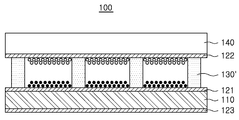
도 1은 마이크로 캡슐을 이용한 본 개시의 일 실시 예에 따른 전자 종이 표시 장치의 개략적인 단면도를 도시한 것이다.
도 2는 마이크로 컵을 이용한 본 개시의 일 실시 예에 따른 전자 종이 표시 장치의 개략적인 단면도를 도시한 것이다.
도 3은 본 개시의 다른 실시 예에 따른 전자 종이 표시 장치의 개략적인 단면도를 도시한 것이다.
도 4는 본 개시의 보호층, 제3 및 제4 전극이 배치된 다른 실시 예에 따른 전자 종이 표시 장치의 개략적인 단면도를 도시한 것이다.1 shows a schematic cross-sectional view of an electronic paper display device according to one embodiment of the present disclosure using microcapsules.
Figure 2 shows a schematic cross-sectional view of an electronic paper display device according to one embodiment of the present disclosure using a microcup.
Figure 3 shows a schematic cross-sectional view of an electronic paper display device according to another embodiment of the present disclosure.
Fig. 4 shows a schematic cross-sectional view of an electronic paper display device according to another embodiment in which the protective layer, third and fourth electrodes of the present disclosure are disposed.
이하, 첨부된 도면을 참조하여 본 발명의 바람직한 실시형태를 설명한다. 다만, 본 발명의 실시형태는 여러 가지 다른 형태로 변형될 수 있으며, 본 발명의 범위가 이하 설명하는 실시형태로 한정되는 것은 아니다. 또한, 본 발명의 실시형태는 당 업계에서 평균적인 지식을 가진 자에게 본 발명을 더욱 완전하게 설명하기 위해서 제공되는 것이다. 따라서, 도면에서의 요소들의 형상 및 크기 등은 보다 명확한 설명을 위해 과장될 수 있으며, 도면상의 동일한 부호로 표시되는 요소는 동일한 요소이다.
Hereinafter, preferred embodiments of the present invention will be described with reference to the accompanying drawings. However, the embodiments of the present invention may be modified into various other forms, and the scope of the present invention is not limited to the embodiments described below. Furthermore, embodiments of the present invention are provided to more fully explain the present invention to those skilled in the art. Accordingly, the shapes and sizes of the elements in the drawings may be exaggerated for clarity of description, and the elements denoted by the same reference numerals in the drawings are the same elements.
전자 종이 표시 장치Electronic paper display device
도 1은 마이크로 캡슐을 이용한 본 개시의 일 실시 예에 따른 전자 종이 표시 장치(100)의 개략적인 단면도를 도시한 것이다.1 shows a schematic cross-sectional view of an electronic
도 1을 참조하면, 본 개시의 일 실시 예에 따른 전자 종이 표시 장치(100)는 제1 전극(121)이 형성된 하부 압전체 기판(110), 표시 소자(130) 및 제2 전극(122)이 형성된 상부 기판(140)을 포함한다.1, an
하부 압전체 기판(110)에는 제1 전극(121)이 형성되어 있다.A
제1 전극(121)의 형성 위치는 특별히 제한되지 않으며, 도시된 바와 같이 표시 소자(130)로 향하는 하부 압전체 기판(110)의 일면에 형성되거나, 하부 압전체 기판(110)의 내부에 형성될 수도 있다.The position of the
하부 압전체 기판(110)은 투명 압전체를 이용하여 형성될 수 있다.The lower
투명 압전체의 재료로는 폴리비닐이딘 플루오라이드, 능동 섬유 복합재 또는 압전 섬유 복합재로 이루어진 군에서 선택되는 적어도 하나로 형성될 수 있다.The transparent piezoelectric material may be formed of at least one selected from the group consisting of polyvinylidene fluoride, an active fiber composite, or a piezoelectric fiber composite.
본 개시의In the present disclosure
제1 전극(121)은 도전성 재료로써, 본 발명의 기술분야에서 통상적으로 사용되는 전극재료를 사용할 수 있다.The
예를 들면, 폴리티오핀 또는 폴리아닐린과 같은 도전성 폴리머, 은이나 니켈과 같은 금속입자, 상기 금속 입자를 포함하는 폴리머 필름, 인듐 틴 옥사이드(ITO: Indium-Tin-Oxide) 등을 사용할 수 있다.
For example, a conductive polymer such as polythiophene or polyaniline, metal particles such as silver or nickel, a polymer film containing the metal particles, and indium-tin-oxide (ITO) may be used.
제1 전극(121)의 상부에는 복수의 표시 소자(130)가 형성될 수 있다.A plurality of
도 1에는 마이크로 캡슐(130)을 이용한 전자 종이 표시 장치를 도시하고 있으며, 도 2는 마이크로 컵(130`)을 이용한 전자 종이 표시 장치를 도시하고 있다.FIG. 1 shows an electronic paper display device using a
마이크로 캡슐에는 분산액과 적어도 두 개 이상의 색을 가지는 표시 입자가 봉지제 안에 형성되며, 마이크로 캡슐은 격벽 내에 분샌액과 적어도 두 개 이상의 색을 가지는 표시 입자가 격벽 내에 형성된다.
In the microcapsule, a dispersion and display particles having at least two or more colors are formed in the encapsulant. In the microcapsule, an encapsulating liquid and display particles having at least two or more colors are formed in the partition wall.
봉지제는 투명한 물질로서, 또한, 봉지제를 형성하는 재료로서는, 폴리우레탄, 폴리 요소, 폴리요소 폴리우레탄, 요소-포름알데하이드 수지, 멜라민-포름알데하이드 수지, 폴리아미드, 폴리에스테르, 폴리 설폰아미드, 폴리카보네이트, 폴리술피네이트, 에폭시리, 아크릴산 에스테르, 메타크릴산 에스테르, 초산비닐, 젤라틴 등을 사용할 수 있으나, 이에 제한되는 것은 아니다.
The encapsulant is a transparent material. Examples of the material for forming the encapsulant include polyurethane, polyurethane, polyurea polyurethane, urea-formaldehyde resin, melamine-formaldehyde resin, polyamide, polyester, polysulfonamide, Polycarbonate, polysulfinate, epoxy resin, acrylic acid ester, methacrylic acid ester, vinyl acetate, gelatin, and the like.
표시 소자(130)의 봉지제 내에는 분산액이 충전된다.The dispersion liquid is filled in the sealing agent of the
분산액은 방향족 탄화수소로서 벤젠, 톨루엔, 크실렌, 에틸벤젠, 도데실 벤젠 등의 알킬 벤젠 유도체, 페닐 크시릴 에탄,1,1-지트리르에탄,1,2-지트리르에탄,1,2-비스(3,4-디메틸 페닐 에탄)(BDMF) 등의 디알릴 알칸 유도체, 디이소프로필 나프탈렌 등의 알킬 나프탈렌 유도체, 물건 이소프로필 페닐, 이소프로필 페닐, ISO 아밀 비페닐 등의 알킬비페닐 유도체, 각종 비율에서 수소화 된 터페닐 유도체, 디벤질 톨루엔 등의 트리아릴지메탄 유도체, 벤질 나프탈렌 유도체, 페닐렌옥사이드 유도체지아르리알킬렌 유도체, 알릴 인 댄유도체, 폴리 염소화 비페닐 유도체, 나프텐계 탄화수소등을 들 수 있다. 또한, 헥산, 사이클로헥산, 케로신, 아이소바, 파라핀계 탄화수소등의 지방족탄화수소류, 클로로포름, 트리클로로 에틸렌, 테트라 클로로 에틸렌, 트리플루오로 에틸렌, 테트라 플루오로 에틸렌, 디클로로 메탄, 취화에틸등의 할로겐화 탄화수소류, 인산 새 크레 질, 인산 트리옥틸, 인산 옥틸 디페닐, 인산 트리사이클로 헥실 등의 인산 에스테르류, 프탈산디 부틸, 프탈산디옥틸, 프탈산디 우라실, 프탈산디 사이클로헥실 등의 프탈산 에스테르류, 올레산 부틸, 디에틸렌글리콜디벤조에이트, 세바스산 디옥틸, 세박산 디뷰틸, 아디프산 디옥틸트리멜리트산 트리옥틸, 쿠엔산 아세틸트리에틸, 말레산 옥틸, 말레인산 디 부틸, 초산에틸등의 카르복실산 에스테르류, 염소화 파라핀, N, N-디부틸-2-부톡시-5-터셔리옥틸 아닐린 등을 들 수 있다.The dispersion liquid may be an aromatic hydrocarbon such as an alkylbenzene derivative such as benzene, toluene, xylene, ethylbenzene or dodecylbenzene, phenylcyclohexane, 1,1-ditertirethane, 1,2- Diallylalkane derivatives such as bis (3,4-dimethylphenylethane) (BDMF), alkyl naphthalene derivatives such as diisopropyl naphthalene, alkyl biphenyl derivatives such as isopropyl phenyl, isopropyl phenyl and ISO amyl biphenyl, Terphenyl derivatives such as dibenzyltoluene and the like, benzyl naphthalene derivatives, phenylene oxide derivative gyre-alkylene derivatives, allylene dane derivatives, polychlorinated biphenyl derivatives, naphthenic hydrocarbons, etc. . In addition, aliphatic hydrocarbons such as hexane, cyclohexane, kerosene, isobar and paraffinic hydrocarbons, halogenated compounds such as chloroform, trichlorethylene, tetrachlorethylene, trifluoroethylene, tetrafluoroethylene, dichloromethane, Phthalic acid esters such as dicyclohexyl phthalate, phthalic acid diacyl phthalate, dicyclohexyl phthalate, and the like, phosphoric acid esters such as oleic acid Butyl, diethylene glycol dibenzoate, dioctyl sebacate, dibutyl sebacate, trioctyl dioctyltrimethylolmellitate, acetyltriethyl citrate, dodecyl maleate, dibutyl maleate, ethyl acetate and the like Acid esters, chlorinated paraffin, and N, N-dibutyl-2-butoxy-5-tertiary octyl aniline.
분산액은 상기의 것으로 한정되는 것은 아니며, 상기의 분산액을 단독으로, 또는 2종 이상을 혼합해 사용할 수 있다.
The dispersion liquid is not limited to those described above, and the dispersion liquid may be used alone or in combination of two or more.
표시 소자(130)에는 백색의 표시 입자와 흑색의 표시 입자가 분산액에 분산되어 있을 수 있다.The
표시 입자는 무기 또는 유기 안료 입자를 이용하여 형성될 수 있다.The display particles can be formed using inorganic or organic pigment particles.
무기 안료 입자로서는, 백연, 아연화, 리토폰, 이산화티탄, 유화아연, 산화 안티몬, 탄산칼슘, 카올린, 운모, 황산바륨, 글로스 화이트, 알루미나 화이트, 탈크, 실리카, 규산 칼슘, 카드뮴 옐로우, 카드뮴 리토폰 화이트, 황색 산화철, 티탄 옐로우, 티탄 바륨 옐로우, 카드뮴 오렌지, 카드뮴 리토폰 오렌지, 모리브데이트오렌지, 적산화철, 연단, 은주홍, 카드뮴 레드, 카드뮴 리토폰 레드, 엠버, 갈색 산화철, 아연철 크롬 브라운, 크롬 그린, 산화크로뮴, 피리지안, 코발트 그린, 코발트 크롬 그린, 티탄 코발트 그린, 감청코발트 블루, 군청, 세르리안브르,코발트 알루미늄 크롬 블루, 코발트 바이올렛, 미네랄 바이올렛, 카본 블랙, 철흑, 망간 페라이트 블랙, 코발트페라이트 블랙, 동 크롬 블랙, 동 크롬 망간 블랙, 흑색 낮은 차원 산화티탄(티탄블랙), 알루미늄 가루, 동분, 연분, 주석가루, 아연 가루 등을 사용할 수 있다.Examples of the inorganic pigment particles include white pigments such as white pigments, zinc pigments, lithopone, titanium dioxide, zinc oxide, antimony oxide, calcium carbonate, kaolin, mica, barium sulfate, gloss white, alumina white, talc, silica, calcium silicate, cadmium red, White iron oxide, titanium yellow, titanium barium yellow, cadmium orange, cadmium ritofone orange, morbidate orange, red iron oxide, podium, scarlet red, cadmium red, cadmium ritofone red, amber, brown iron oxide, Cobalt blue, cobalt aluminum chromium blue, cobalt violet, minerals violet, carbon black, iron black, manganese ferrite black, cobalt chrome green, chromium oxide, pyridine, cobalt green, cobalt chrome green, titanium cobalt green, Cobalt ferrite black, copper chrome black, copper chromium manganese black, black low-dimensional titanium oxide (titanium black), aluminum It may be the flour, dongbun, ROCK, tin powder, zinc powder and the like.
또한, 유기안료 입자로서는, 퍼스트 옐로우, 디스아조 옐로우, 축합 아조이에로, 안트라피리미딘 옐로우, ISO 인돌린 옐로우, 동 아조메틴 옐로우, 키노프탈로인이에로, 벤즈아미다졸론 옐로우, 니켈 디옥심 옐로우, 모노아조 옐로우 레이크, 디니트로아닐린 오렌지, 피라졸론 오렌지, 페리논 오렌지, 나프톨 레드, 톨루이딘 레드, 파마넨트카민, 브릴리언트 퍼스트 스카 레드, 피라졸론 레드, 퍼머넌트 레드, 리소르렛드, 본 레이크 레드, 레이크 레드, 브리리안트카민, 나프톨 레드, 퀴나크리돈 마젠타축합 아조렛드, 나프토르카민, 페릴렌 스카 레드, 축합 아조스카렛드, 벤즈이미다조론카민, 안트라퀴놀릴 레드, 페릴렌 레드, 페리렌마룬, 키나크리돈마룬, 퀴나크리돈 스카 레드, 퀴나크리돈레드, 디케토피롤로피롤 레드, 벤즈아미다졸론 브라운, 프탈로시아닌 그린, 빅토리아 블루 레이크, 프탈로시아닌 블루, 퍼스트 스카이브 루, 알칼리브르토나, 인 댄 트론 블루, 메틸 바이올렛 레이크, 디옥사진 바이올렛, 나프톨 바이올렛 등을 사용할 수 있다.
Examples of the organic pigment particles include first yellow, disazo yellow, condensed azoiron, anthrapyrimidine yellow, ISO indoline yellow, copper azomethine yellow, quinophthaloin yellow, benzamidazolone yellow, Wherein the coloring agent is selected from the group consisting of yellow, monoazo yellow lake, dinitroaniline orange, pyrazolone orange, perinone orange, naphthol red, toluidine red, pamanendocarmin, brilliant first skarred, pyrazolone red, permanent red, lisorred, But are not limited to, lake red, brilliant carmine, naphthol red, quinacridone magenta condensate azoled, naphthocarmin, perylenescal red, condensed azoscarrad, benzimidazolonamine, anthraquinolyl red, perylene red, Maroon, quinacridone maroon, quinacridone scarlet, quinacridone red, diketopyrrolopyrrole red, benzamidazolone brown, phthaloic acid Nin green, you can use the Victoria blue lake, phthalocyanine blue, first skive base, alkaline Libreville tona, Dan Tron blue, methyl violet lake, dioxazine violet, violet-naphthol and the like.
표시 소자(130)의 상부에는 제2 전극(122) 배치될 수 있다.The
제2 전극(122)은 상부 기판(140)에 형성되어, 표시 소자(130)의 상부에 배치될 수 있다.The
제2 전극(122)은 제1 전극(121)과 동일한 재료로 형성될 수 있다.The
상부 기판(140)은 표시면으로 제공될 수 있으므로, 투명 물질로 이루어지는 것이 바람직하다.Since the
본 개시에서 투명물질의 광투과도는 시인성을 저하시키지 않는 범위 내에서 정할 수 있으며, 예를 들면 광투과도가 85% 이상인 물질로 형성될 수 있다.In the present disclosure, the light transmittance of the transparent material can be determined within a range that does not deteriorate the visibility, and for example, it can be formed of a material having a light transmittance of 85% or more.
상부 기판(140)은 유리 또는 유연성이 있는 플라스틱 종류로 이루어질 수 있다. 상기 플라스틱은 이에 제한되는 것은 아니나, 예를 들면, 폴리에틸렌테레프탈레이트(PET), 폴리카보네이트(PC), 또는 폴리메틸메타아크릴레이트(PMMA), 폴리에틸렌나프탈레이트(PEN), 폴리에테르술폰(PES), 고리형 올레핀 고분자(COC), 폴리디메틸실록산(PDMS, polydimethylsiloxane) 또는 폴리우레탄 아크릴레이트(PUA, poly urethane acrylate) 등을 사용할 수 있다.
The
표시 소자(130)에 포함되어 있는 표시 입자는 그 크기가 매우 작아, 뭉침 현상이 발생하게 된다.The display particles included in the
이러한 뭉침 현상을 해결하기 위해, 전자 종이 표시 장치가 구동하는 초기에 DC 전압과 함께 AC 전압을 인가해 준다. 하지만, 이러한 AC 전압의 인가만으로는 표시 입자의 뭉침 현상이 완전히 해결되지 못하는 문제가 있다.In order to solve this aggregation phenomenon, an AC voltage is applied together with a DC voltage at the initial stage when the electronic paper display device is driven. However, there is a problem that the agglomeration phenomenon of the display particles can not be completely solved only by the application of the AC voltage.
본 개시의 일 실시예에 따른 전자 종이 표시 장치는 하부 압전체 기판(110)에서 물리적 진동을 발생시키기 때문에, 표시 입자의 뭉침 현상을 빠르고 완전하게 해결할 수 있다.Since the electronic paper display device according to the embodiment of the present disclosure generates physical vibration in the lower
따라서 본 개시의 일 실시 예에 따른 전자 종이 표시 장치는 이에 따라 기존의 전자 종이 표시 장치에 비해 낮은 전압에서 구동이 가능하며, 표시 입자의 뭉침 방지를 통해 명암비를 향상시킬 수 있다.
Accordingly, the electronic paper display device according to an embodiment of the present disclosure can drive at a lower voltage than conventional electronic paper display devices, and can prevent the display particles from aggregating, thereby improving the contrast ratio.
하부 압전체 기판(110)의 하부에는 제3 전극(123)이 형성될 수 있다.A
제3 전극(123)은 제2 전극(122)과 전기적으로 연결되어, 전자 종이 표시 장치의 구동 초기에 AC 전압이 인가될 때, 압전체에도 이러한 AC 전압이 동시에 인가됨으로써 AC 전압과 물리전 진동이 동시에 발생하도록 유도할 수 있다.
The
도 3은 본 개시의 다른 실시 예에 따른 전자 종이 표시 장치(200)의 개략적인 단면도를 도시한 것이다.Fig. 3 shows a schematic cross-sectional view of an electronic
이하, 도 3에서는 도 1 및 2의 전자 종이 표시 장치(100)와 차이점에 대해서 설명하도록 한다.3, differences from the electronic
도 3을 참조하면, 도 1의 상부 기판(140)과 달리, 본 개시의 다른 실시 예에 따른 전조 종이 표시 장치는 상부 압전체 기판(240)이 배치될 수 있다.Referring to FIG. 3, unlike the
상부 압전체 기판(240)은 투명 압전체로 형성될 수 있다.The upper
상부 압전체 기판(240)은 표시면으로 제공될 수 있으므로, 투명 물질로 이루어지는 것이 바람직하다.Since the upper
상부 압전체 기판(240)은 투명 압전체를 이용하여 형성될 수 있다.The upper
투명 압전체의 재료로는 폴리비닐이딘 플루오라이드, 능동 섬유 복합재 또는 압전 섬유 복합재로 이루어진 군에서 선택되는 적어도 하나로 형성될 수 있다.The transparent piezoelectric material may be formed of at least one selected from the group consisting of polyvinylidene fluoride, an active fiber composite, or a piezoelectric fiber composite.
본 개시에서 투명 압전체 재료의 광투과도는 시인성을 저하시키지 않는 범위 내에서 정할 수 있으며, 예를 들면 광투과도가 85% 이상인 물질로 형성될 수 있다.In the present disclosure, the light transmittance of the transparent piezoelectric material can be determined within a range that does not deteriorate the visibility, and can be formed of, for example, a material having a light transmittance of 85% or more.
상부 기판을 상부 압전체 기판(240)으로 형성함으로써, 표시 입자의 뭉침 현상을 보다 더 빠르게 해소할 수 있으며, 이에 따라 전자 종이 표시 장치의 명암비가 향상될 수 있다.
By forming the upper substrate with the upper
도 4는 본 개시의 보호층 및 압전체용 전극이 배치된 다른 실시 예에 따른 전자 종이 표시 장치(200)의 개략적인 단면도를 도시한 것이다.Fig. 4 shows a schematic cross-sectional view of an electronic
도 4를 참조하면, 하부 압전체 기판(210)의 하부에는 제3 전극(223)이 형성될 수 있으며, 상부 압전체 기판(240)의 상부에는 제4 전극(224)이 형성될 수 있다.4, a
제3 및 제4 전극(223, 224)는 제1 및 제2 전극(221, 222)와 동일한 투명 전극 재료로 형성될 수 있다.The third and
제3 전극(223)은 제2 전극(222)과 전기적으로 연결되고, 제4 전극(224)은 제1 전극(221)과 전기적으로 연결되어, 각각 하부 압전체 기판(210)과 상부 압전체 기판(240)에 압전 현상을 유도할 수 있다.The
즉, 전자 종이 표시 장치의 구동 초기에 표시 소자(240)에 AC 전압이 인가될 때, 동시에 하부 압전체 기판(210)과 상부 압전체 기판(240)에 압전 현상을 유도할 수 있다.That is, when the AC voltage is applied to the
이에 따라, AC 전압에 의한 표시 입자의 뭉침 현상 해소가, 압전체 기판(210, 240)의 물리적 진동에 의해 더욱 빠르게 발생할 수 있다.
Accordingly, the agglomeration of the display particles due to the AC voltage can be solved more quickly by the physical vibrations of the
제4 전극(224) 또는 상부 압전체 기판(240)의 상부에는 보호층(250)이 형성될 수 있다.A
상부 압전체 기판(240)이 표시면으로 제공되는 경우, 충격에 의한 파손 및 오염으로 인한 손상을 방지하기 보호층(250)이 형성될 수 있으며, 보호층(250)은 투명한 재질로 형성할 수 있다.
When the upper
본 개시는 전자 종이 표시 장치 중 마이크로 캡슐 및 마이크로 컵을 이용하는 방법을 중심으로 설명하였으나, 트위스트 볼 등의 방법을 이용하는 전자 종이 표시 장치에도 치환, 변형 및 변경하여 사용할 수 있다.
Although the present disclosure has been mainly described with reference to a method using microcapsules and microcups in an electronic paper display device, it is also possible to substitute, modify and change the electronic paper display device using a twist ball method or the like.
본 개시는 상술한 실시형태 및 첨부된 도면에 의해 한정되는 것이 아니며, 첨부된 청구범위에 의해 한정하고자 한다. 따라서, 청구범위에 기재된 본 발명의 기술적 사상을 벗어나지 않는 범위 내에서 당 기술분야의 통상의 지식을 가진 자에 의해 다양한 형태의 치환, 변형 및 변경이 가능할 것이며, 이 또한 본 발명의 범위에 속한다고 할 것이다.
The present disclosure is not limited by the above-described embodiments and the accompanying drawings, but is intended to be limited by the appended claims. It will be apparent to those skilled in the art that various changes in form and details may be made therein without departing from the spirit and scope of the invention as defined by the appended claims. something to do.
100: 전자 종이 표시 장치
110: 하부 압전체 기판
121: 제1 전극
122: 제2 전극
123: 제3 전극
130: 표시 소자
140: 상부 기판100: Electronic paper display device
110: Lower piezoelectric substrate
121: first electrode
122: second electrode
123: third electrode
130: display element
140: upper substrate
Claims (10)
상기 하부 압전체 기판의 상부에 배치되는 복수의 표시 소자; 및
상기 표시 소자 상부에 배치되는 제2 전극;을 포함하는 전자 종이 표시 장치.
A lower piezoelectric substrate on which a first electrode is disposed on an upper surface;
A plurality of display elements disposed on the lower piezoelectric substrate; And
And a second electrode disposed on the display element.
상기 표시 소자는 마이크로 캡슐 또는 마이크로 컵인 전자 종이 표시 장치.
The method according to claim 1,
Wherein the display element is a microcapsule or a microcup.
상기 하부 압전체 기판은 투명 압전체로 형성되는 전자 종이 표시 장치.
The method according to claim 1,
Wherein the lower piezoelectric substrate is formed of a transparent piezoelectric material.
상기 투명 압전체는 폴리비닐이딘 플루오라이드, 능동 섬유 복합재 또는 압전 섬유 복합재로 이루어진 군에서 선택되는 적어도 하나로 형성되는 전자 종이 표시 장치.
The method of claim 3,
Wherein the transparent piezoelectric material is formed of at least one selected from the group consisting of polyvinylidene fluoride, an active fiber composite material, and a piezoelectric fiber composite material.
상기 하부 압전체 기판의 하면에 형성되는 제3 전극을 더 포함하는 전자 종이 표시 장치.
The method according to claim 1,
And a third electrode formed on the lower surface of the lower piezoelectric substrate.
상기 제2 전극의 상부에 배치되는 상부 압전체 기판을 더 포함하는 전자 종이 표시 장치.
The method according to claim 1,
And an upper piezoelectric substrate disposed above the second electrode.
상기 상부 압전체 기판은 투명 압전체로 형성되는 전자 종이 표시 장치.
The method according to claim 6,
Wherein the upper piezoelectric substrate is formed of a transparent piezoelectric material.
상기 투명 압전체는 폴리비닐이딘 플루오라이드, 능동 섬유 복합재 또는 압전 섬유 복합재로 이루어진 군에서 선택되는 적어도 하나로 형성되는 전자 종이 표시 장치.
8. The method of claim 7,
Wherein the transparent piezoelectric material is formed of at least one selected from the group consisting of polyvinylidene fluoride, an active fiber composite material, and a piezoelectric fiber composite material.
상기 상부 압전체 기판의 상부에 배치되는 제3 전극을 포함하는 전자 종이 표시 장치.
The method according to claim 6,
And a third electrode disposed on the upper piezoelectric substrate.
상기 제3 전극의 상부에 배치되는 보호층을 더 포함하는 전자 종이 표시 장치.
10. The method of claim 9,
And a protective layer disposed on the third electrode.
Priority Applications (1)
| Application Number | Priority Date | Filing Date | Title |
|---|---|---|---|
| KR1020150010567A KR20160090588A (en) | 2015-01-22 | 2015-01-22 | Electronic paper display device |
Applications Claiming Priority (1)
| Application Number | Priority Date | Filing Date | Title |
|---|---|---|---|
| KR1020150010567A KR20160090588A (en) | 2015-01-22 | 2015-01-22 | Electronic paper display device |
Publications (1)
| Publication Number | Publication Date |
|---|---|
| KR20160090588A true KR20160090588A (en) | 2016-08-01 |
Family
ID=56706830
Family Applications (1)
| Application Number | Title | Priority Date | Filing Date |
|---|---|---|---|
| KR1020150010567A Withdrawn KR20160090588A (en) | 2015-01-22 | 2015-01-22 | Electronic paper display device |
Country Status (1)
| Country | Link |
|---|---|
| KR (1) | KR20160090588A (en) |
Cited By (4)
| Publication number | Priority date | Publication date | Assignee | Title |
|---|---|---|---|---|
| WO2018076703A1 (en) * | 2016-10-28 | 2018-05-03 | 京东方科技集团股份有限公司 | Reflective display and manufacturing method therefor |
| WO2020036908A1 (en) * | 2018-08-14 | 2020-02-20 | E Ink California, Llc | Piezo electrophoretic display |
| JP2021517671A (en) * | 2018-05-17 | 2021-07-26 | イー インク カリフォルニア, エルエルシー | Piezoelectric electrophoresis display |
| US11380272B2 (en) * | 2018-01-02 | 2022-07-05 | Beijing Boe Display Technology Co., Ltd. | Display unit, driving method thereof, and display device |
Citations (1)
| Publication number | Priority date | Publication date | Assignee | Title |
|---|---|---|---|---|
| JP2013238862A (en) | 2005-01-26 | 2013-11-28 | E Ink Corp | Electrophoretic display using gaseous fluid |
-
2015
- 2015-01-22 KR KR1020150010567A patent/KR20160090588A/en not_active Withdrawn
Patent Citations (1)
| Publication number | Priority date | Publication date | Assignee | Title |
|---|---|---|---|---|
| JP2013238862A (en) | 2005-01-26 | 2013-11-28 | E Ink Corp | Electrophoretic display using gaseous fluid |
Cited By (10)
| Publication number | Priority date | Publication date | Assignee | Title |
|---|---|---|---|---|
| WO2018076703A1 (en) * | 2016-10-28 | 2018-05-03 | 京东方科技集团股份有限公司 | Reflective display and manufacturing method therefor |
| US10503006B2 (en) | 2016-10-28 | 2019-12-10 | Boe Technology Group Co., Ltd. | Reflective display and preparation method thereof |
| US11380272B2 (en) * | 2018-01-02 | 2022-07-05 | Beijing Boe Display Technology Co., Ltd. | Display unit, driving method thereof, and display device |
| JP2021517671A (en) * | 2018-05-17 | 2021-07-26 | イー インク カリフォルニア, エルエルシー | Piezoelectric electrophoresis display |
| JP2022078156A (en) * | 2018-05-17 | 2022-05-24 | イー インク カリフォルニア, エルエルシー | Piezo-electrophoretic display |
| EP3794410B1 (en) * | 2018-05-17 | 2024-01-24 | E Ink Corporation | Method of producing a piezo electrophoretic display |
| US11892740B2 (en) | 2018-05-17 | 2024-02-06 | E Ink Corporation | Piezo electrophoretic display |
| US12298645B2 (en) | 2018-05-17 | 2025-05-13 | E Ink Corporation | Piezo electrophoretic display |
| WO2020036908A1 (en) * | 2018-08-14 | 2020-02-20 | E Ink California, Llc | Piezo electrophoretic display |
| US11493821B2 (en) | 2018-08-14 | 2022-11-08 | E Ink California, Llc | Piezo electrophoretic display |
Similar Documents
| Publication | Publication Date | Title |
|---|---|---|
| TWI631405B (en) | Electrophoretic display device | |
| CN101542383B (en) | Electrophoretic fluid, electrophoretic display medium, electrophoretic display element, and electrophoretic display device | |
| EP3210076B1 (en) | Driving method for a color electrophoretic display | |
| EP1923733B1 (en) | Color filter substrate and electrophoretic display device having the same | |
| JP6751148B2 (en) | Polyhydroxy composition for sealing electrophoretic displays | |
| JP2022186978A (en) | Electro-optical display and driving method | |
| TWI724486B (en) | Flexible encapsulated electro-optic media | |
| CN102272672A (en) | Electrophoretic liquid, image display medium, and image display device | |
| KR20160090588A (en) | Electronic paper display device | |
| JP5118121B2 (en) | Electronic paper display device and manufacturing method thereof | |
| TWI748273B (en) | Electro-optic device and method of operating the same | |
| CN1989446A (en) | Panel for information display and information display | |
| KR20160090597A (en) | Electronic paper display device and manufacturing method thereof | |
| CN116601560A (en) | Electrophoretic media containing fluorescent particles | |
| JP5326695B2 (en) | Image display method | |
| JP5579763B2 (en) | Electronic paper display device and manufacturing method thereof | |
| KR102264872B1 (en) | Display Panel and Method of Driving the Same | |
| JP2005352423A (en) | Electrophoretic particles, electrophoretic display dispersion, and electrophoretic display device | |
| JP2006113438A (en) | Electrophoretic display device, charged electrophoretic particles for electrophoretic display, and dispersion liquid for electrophoretic display | |
| KR20170084821A (en) | Display device and manufacturing method of the same | |
| HK40089751A (en) | Electrophoretic medium including fluorescent particles | |
| JP2006195378A (en) | Electrophoretic particles, electrophoretic display dispersion, and electrophoretic display device | |
| JP2003315845A (en) | Electrophoretic display panel and method of manufacturing the same | |
| KR20120089988A (en) | Display devices | |
| CN101160546A (en) | information display panel |
Legal Events
| Date | Code | Title | Description |
|---|---|---|---|
| PA0109 | Patent application |
Patent event code: PA01091R01D Comment text: Patent Application Patent event date: 20150122 |
|
| PG1501 | Laying open of application | ||
| PC1203 | Withdrawal of no request for examination | ||
| WITN | Application deemed withdrawn, e.g. because no request for examination was filed or no examination fee was paid |