KR20160071579A - Organic layer deposition assembly, apparatus for organic layer deposition comprising the same, and method for manufacturing of organic light emitting display apparatus using the same - Google Patents
Organic layer deposition assembly, apparatus for organic layer deposition comprising the same, and method for manufacturing of organic light emitting display apparatus using the same Download PDFInfo
- Publication number
- KR20160071579A KR20160071579A KR1020140178702A KR20140178702A KR20160071579A KR 20160071579 A KR20160071579 A KR 20160071579A KR 1020140178702 A KR1020140178702 A KR 1020140178702A KR 20140178702 A KR20140178702 A KR 20140178702A KR 20160071579 A KR20160071579 A KR 20160071579A
- Authority
- KR
- South Korea
- Prior art keywords
- substrate
- evaporation source
- organic layer
- deposition
- patterning slit
- Prior art date
- Legal status (The legal status is an assumption and is not a legal conclusion. Google has not performed a legal analysis and makes no representation as to the accuracy of the status listed.)
- Granted
Links
Images


Classifications
-
- H—ELECTRICITY
- H10—SEMICONDUCTOR DEVICES; ELECTRIC SOLID-STATE DEVICES NOT OTHERWISE PROVIDED FOR
- H10K—ORGANIC ELECTRIC SOLID-STATE DEVICES
- H10K71/00—Manufacture or treatment specially adapted for the organic devices covered by this subclass
-
- H—ELECTRICITY
- H10—SEMICONDUCTOR DEVICES; ELECTRIC SOLID-STATE DEVICES NOT OTHERWISE PROVIDED FOR
- H10K—ORGANIC ELECTRIC SOLID-STATE DEVICES
- H10K59/00—Integrated devices, or assemblies of multiple devices, comprising at least one organic light-emitting element covered by group H10K50/00
-
- Y—GENERAL TAGGING OF NEW TECHNOLOGICAL DEVELOPMENTS; GENERAL TAGGING OF CROSS-SECTIONAL TECHNOLOGIES SPANNING OVER SEVERAL SECTIONS OF THE IPC; TECHNICAL SUBJECTS COVERED BY FORMER USPC CROSS-REFERENCE ART COLLECTIONS [XRACs] AND DIGESTS
- Y02—TECHNOLOGIES OR APPLICATIONS FOR MITIGATION OR ADAPTATION AGAINST CLIMATE CHANGE
- Y02E—REDUCTION OF GREENHOUSE GAS [GHG] EMISSIONS, RELATED TO ENERGY GENERATION, TRANSMISSION OR DISTRIBUTION
- Y02E10/00—Energy generation through renewable energy sources
- Y02E10/50—Photovoltaic [PV] energy
- Y02E10/549—Organic PV cells
-
- Y—GENERAL TAGGING OF NEW TECHNOLOGICAL DEVELOPMENTS; GENERAL TAGGING OF CROSS-SECTIONAL TECHNOLOGIES SPANNING OVER SEVERAL SECTIONS OF THE IPC; TECHNICAL SUBJECTS COVERED BY FORMER USPC CROSS-REFERENCE ART COLLECTIONS [XRACs] AND DIGESTS
- Y02—TECHNOLOGIES OR APPLICATIONS FOR MITIGATION OR ADAPTATION AGAINST CLIMATE CHANGE
- Y02P—CLIMATE CHANGE MITIGATION TECHNOLOGIES IN THE PRODUCTION OR PROCESSING OF GOODS
- Y02P70/00—Climate change mitigation technologies in the production process for final industrial or consumer products
- Y02P70/50—Manufacturing or production processes characterised by the final manufactured product
Landscapes
- Engineering & Computer Science (AREA)
- Manufacturing & Machinery (AREA)
- Electroluminescent Light Sources (AREA)
- Physical Vapour Deposition (AREA)
Abstract
Description
본 발명의 실시예들은 장치 및 방법에 관한 것으로서, 더 상세하게는 유기층 증착 어셈블리, 이를 포함하는 유기층 증착 장치 및 이를 이용한 유기 발광 디스플레이 장치의 제조 방법에 관한 것이다.Embodiments of the present invention relate to an apparatus and method, and more particularly, to an organic layer deposition assembly, an organic layer deposition apparatus including the organic layer deposition assembly, and a method of manufacturing an organic light emitting display using the same.
디스플레이 장치들 중, 유기 발광 디스플레이 장치는 시야각이 넓고 컨트라스트가 우수할 뿐만 아니라 응답속도가 빠르다는 장점을 가지고 있어 차세대 디스플레이 장치로서 주목을 받고 있다. Of the display devices, the organic light emitting display device has a wide viewing angle, excellent contrast, and fast response speed, and is receiving attention as a next generation display device.
유기 발광 디스플레이 장치는 서로 대향된 제1 전극 및 제2 전극 사이에 발광층 및 이를 포함하는 중간층을 구비한다. 이때 상기 전극들 및 중간층은 여러 방법으로 형성될 수 있는데, 그 중 한 방법이 독립 증착 방식이다. 증착 방법을 이용하여 유기 발광 디스플레이 장치를 제작하기 위해서는, 유기층 등이 형성될 기판 면에, 형성될 유기층 등의 패턴과 동일한 패턴을 가지는 파인 메탈 마스크(fine metal mask: FMM)를 밀착시키고 유기층 등의 재료를 증착하여 소정 패턴의 유기층을 형성한다.The organic light emitting display device includes a light emitting layer and an intermediate layer including the light emitting layer between the first electrode and the second electrode facing each other. At this time, the electrodes and the intermediate layer can be formed by various methods, one of which is the independent deposition method. In order to manufacture an organic light emitting display device using a deposition method, a fine metal mask (FMM) having the same pattern as that of an organic layer to be formed is closely contacted to a substrate surface on which an organic layer or the like is to be formed, A material is deposited to form an organic layer of a predetermined pattern.
그러나, 이러한 파인 메탈 마스크를 이용하는 방법은 대형의 마더 글래스(mother-glass)를 사용하여 유기 발광 디스플레이 장치를 대면적화하기에는 부적합하다는 한계가 있다. 왜냐하면, 대면적 마스크를 사용하면 자중에 의해 마스크의 휨 현상이 발생하는데, 이 휨 현상에 의한 패턴의 왜곡이 발생될 수 있기 때문이다. 이는 패턴에 고정세를 요하는 현 경향과도 배치되는 것이다.However, the method using such a fine metal mask has a limitation that it is not suitable for large-sized organic light emitting display device using a large mother-glass. This is because, when a large area mask is used, the mask is warped due to its own weight, and distortion of the pattern due to the warping phenomenon may occur. This is also arranged with the current tendency to require fixed tax on the pattern.
더욱이, 기판과 파인 메탈 마스크를 얼라인하여 밀착시키고, 증착을 수행한 후, 다시 기판과 파인 메탈 마스크를 분리시키는 과정에서 상당한 시간이 소요되어, 제조 시간이 오래 걸리고 생산 효율이 낮다는 문제점이 존재하였다. Further, there is a problem that it takes a considerable time to separate the substrate and the fine metal mask from each other, and then takes a long time to manufacture and lowers the production efficiency .
전술한 배경기술은 발명자가 본 발명의 도출을 위해 보유하고 있었거나, 본 발명의 도출 과정에서 습득한 기술 정보로서, 반드시 본 발명의 출원 전에 일반 공중에게 공개된 공지기술이라 할 수는 없다.The above-described background technology is technical information that the inventor holds for the derivation of the present invention or acquired in the process of deriving the present invention, and can not necessarily be a known technology disclosed to the general public prior to the filing of the present invention.
본 발명의 실시예들은 유기층 증착 어셈블리, 이를 포함하는 유기층 증착 장치 및 이를 이용한 유기 발광 디스플레이 장치의 제조 방법을 제공한다.Embodiments of the present invention provide an organic layer deposition assembly, an organic layer deposition apparatus including the organic layer deposition assembly, and a method of manufacturing an organic light emitting display device using the same.
본 발명에 일 실시예는 기판에 증착 물질을 증착하기 위한 유기층 증착 어셈블리에 있어서, 증착 물질을 방사하는 증착원과, 증착원의 일측에 배치되며, 복수개의 증착원 노즐들이 형성되는 증착원 노즐부와, 증착원 노즐부와 대향되게 배치되고, 복수개의 패터닝 슬릿들이 형성되는 패터닝 슬릿 시트를 포함하고, 기판은 유기층 증착 어셈블리와 소정 정도 이격되도록 형성되어 유기층 증착 어셈블리에 대하여 상대적으로 이동 가능하도록 형성되고, 증착원에서 방사된 증착 물질은 패터닝 슬릿 시트를 통과하여 기판에 패턴을 형성하면서 증착되며, 복수개의 패터닝 슬릿들은, 패터닝 슬릿의 길이 방향으로 연장 형성되며, 패터닝 슬릿의 길이 방향 및 폭 방향으로 복수개가 연속적으로 배치되어 증착 물질을 통과시키는 복수개의 개구부와, 각 개구부들 사이의 패터닝 슬릿의 길이 방향으로 이격된 공간에 형성되는 복수개의 리브를 구비하며, 각 리브들의 폭은 0.65mm인 것을 특징으로 하는 유기층 증착 어셈블리를 개시한다.One embodiment of the present invention is an organic layer deposition assembly for depositing a deposition material on a substrate, comprising: an evaporation source for emitting a deposition material; an evaporation source nozzle unit disposed at one side of the evaporation source and having a plurality of evaporation source nozzles And a patterning slit sheet disposed to face the evaporation source nozzle portion and having a plurality of patterning slits formed therein, the substrate being formed to be spaced apart from the organic layer deposition assembly to be relatively movable with respect to the organic layer deposition assembly , The deposition material emitted from the evaporation source passes through the patterning slit sheet and is deposited while forming a pattern on the substrate, the plurality of patterning slits extend in the longitudinal direction of the patterning slit, and a plurality of A plurality of openings arranged continuously to allow the deposition material to pass therethrough, Includes a plurality of ribs formed in a space spaced apart in the longitudinal direction of the slit pattern between the width of each rib discloses an organic layer deposition assemblies, characterized in that 0.65mm.
본 실시예에 있어서, 패터닝 슬릿 시트는 패터닝 슬릿 시트의 길이 방향인 제1 방향 및 패터닝 슬릿 시트의 폭 방향인 제2 방향 중 적어도 어느 한 방향에 있어서, 기판보다 작게 형성되는 것을 특징으로 할 수 있다.In the present embodiment, the patterning slit sheet may be formed to be smaller than the substrate in at least one of a first direction, which is a longitudinal direction of the patterning slit sheet, and a second direction, which is a width direction of the patterning slit sheet .
본 실시예에 있어서, 패터닝 슬릿 시트에는 패터닝 슬릿 시트의 길이 방향인 제1 방향을 따라 복수개의 패터닝 슬릿들이 형성되고, 증착원 노즐부에는 패터닝 슬릿 시트의 폭 방향인 제2 방향을 따라 복수개의 증착원 노즐들이 형성되는 것을 특징으로 할 수 있다.In this embodiment, a plurality of patterning slits are formed in the patterning slit sheet along a first direction which is the lengthwise direction of the patterning slit sheet, and a plurality of evaporation slits are formed in the evaporation source nozzle portion along a second direction in the width direction of the patterning slit sheet. And circular nozzles are formed.
본 실시예에 있어서, 증착원 및 증착원 노즐부와 패터닝 슬릿 시트는 연결부재에 의해 결합되어 일체로 형성되는 것을 특징으로 할 수 있다.In the present embodiment, the evaporation source, the evaporation source nozzle unit, and the patterning slit sheet may be integrally formed by a coupling member.
본 실시예에 있어서, 연결부재는 증착 물질의 이동 경로를 가이드 하는 것을 특징으로 할 수 있다.In this embodiment, the connecting member guides the movement path of the evaporation material.
본 실시예에 있어서, 연결부재는 증착원 및 증착원 노즐부와 패터닝 슬릿 시트 사이의 공간을 외부로부터 밀폐하도록 형성되는 것을 특징으로 할 수 있다.In this embodiment, the connecting member may be formed to seal the space between the evaporation source and the evaporation source nozzle portion and the patterning slit sheet from the outside.
본 발명의 다른 실시예는 기판을 고정하며 고정된 기판과 함께 이동 가능하도록 형성된 이동부와, 기판이 고정된 이동부를 제1 방향으로 이동시키는 제1 이송부와, 증착이 완료되어 기판이 분리된 이동부를 제1 방향의 반대 방향으로 이동시키는 제2 이송부를 포함하는 이송부와, 이동부에 기판을 고정시키는 로딩부와, 진공으로 유지되는 챔버와, 로딩부로부터 이송된 이동부에 고정된 기판에 유기층을 증착하는 하나 이상의 유기층 증착 어셈블리를 포함하는 증착부와, 증착부를 통과하면서 증착이 완료된 기판을 상기 이동부로부터 분리시키는 언로딩부를 포함하고, 이동부는 제1 이송부와 제2 이송부 사이를 순환가능하도록 형성되고, 이동부에 고정된 기판은 제1 이송부에 의해 이동되는 동안 유기층 증착 어셈블리와 소정 정도 이격되도록 형성되며, 복수개의 패터닝 슬릿들은, 패터닝 슬릿의 길이 방향으로 연장 형성되며, 패터닝 슬릿의 길이 방향 및 폭 방향으로 복수개가 연속적으로 배치되어 증착 물질을 통과시키는 복수개의 개구부와, 각 개구부들 사이의 패터닝 슬릿의 길이 방향으로 이격된 공간에 형성되는 복수개의 리브를 구비하며, 각 리브들의 폭은 0.65mm인 것을 특징으로 하는 유기층 증착 장치를 개시한다.According to another embodiment of the present invention, there is provided a method of manufacturing a semiconductor device, including: a moving unit configured to move a substrate with a fixed substrate, the moving unit moving the moving unit in a first direction; A loading section for fixing the substrate to the moving section, a chamber for holding the vacuum, and a substrate fixed to the moving section transferred from the loading section, wherein the organic layer And an unloading section for separating the substrate from which the deposition has been completed while passing through the deposition section from the moving section, wherein the moving section is capable of circulating between the first transfer section and the second transfer section And the substrate fixed to the moving part is formed to be spaced apart from the organic layer deposition assembly by a predetermined distance while being moved by the first transfer part A plurality of patterning slits extending in the longitudinal direction of the patterning slit and having a plurality of openings through which a plurality of deposition materials are passed in a longitudinal direction and a width direction of the patterning slit, And a plurality of ribs formed in a space spaced in the longitudinal direction, wherein the width of each of the ribs is 0.65 mm.
본 실시예에 있어서, 제1 이송부와 제2 이송부는 증착부를 통과할 때에 증착부를 관통하도록 구비되는 것을 특징으로 할 수 있다.In this embodiment, the first transfer unit and the second transfer unit may be configured to pass through the vapor deposition unit when passing through the vapor deposition unit.
본 실시예에 있어서, 제1 이송부와 제2 이송부는 상하로 나란히 배치되는 것을 특징으로 할 수 있다.In the present embodiment, the first conveying portion and the second conveying portion may be arranged vertically side by side.
본 실시예에 있어서, 제1 이송부는 이동부를 로딩부, 증착부 및 언로딩부로 순차 이동시키는 것을 특징으로 할 수 있다.In this embodiment, the first transfer unit may be configured to sequentially move the moving unit to the loading unit, the deposition unit, and the unloading unit.
본 실시예에 있어서, 제2 이송부는 이동부를 언로딩부, 증착부 및 로딩부로 순차 이동시시키는 것을 특징으로 할 수 있다.In this embodiment, the second transfer unit may sequentially move the moving unit to the unloading unit, the deposition unit, and the loading unit.
본 실시예에 있어서, 패터닝 슬릿 시트는 패터닝 슬릿 시트의 길이 방향인 제1 방향 및 패터닝 슬릿 시트의 폭 방향인 제2 방향 중 적어도 어느 한 방향에 있어서, 기판보다 작게 형성되는 것을 특징으로 할 수 있다.In the present embodiment, the patterning slit sheet may be formed to be smaller than the substrate in at least one of a first direction, which is a longitudinal direction of the patterning slit sheet, and a second direction, which is a width direction of the patterning slit sheet .
본 실시예에 있어서, 패터닝 슬릿 시트에는 패터닝 슬릿 시트의 길이 방향인 제1 방향을 따라 복수개의 패터닝 슬릿들이 형성되고, 증착원 노즐부에는 패터닝 슬릿 시트의 폭 방향인 제2 방향을 따라 복수개의 증착원 노즐들이 형성되는 것을 특징으로 할 수 있다.In this embodiment, a plurality of patterning slits are formed in the patterning slit sheet along a first direction which is the lengthwise direction of the patterning slit sheet, and a plurality of evaporation slits are formed in the evaporation source nozzle portion along a second direction in the width direction of the patterning slit sheet. And circular nozzles are formed.
본 실시예에 있어서, 증착원 및 증착원 노즐부와 패터닝 슬릿 시트는 연결부재에 의해 결합되어 일체로 형성되는 것을 특징으로 할 수 있다.In the present embodiment, the evaporation source, the evaporation source nozzle unit, and the patterning slit sheet may be integrally formed by a coupling member.
본 실시예에 있어서, 연결부재는 증착 물질의 이동 경로를 가이드 하는 것을 특징으로 할 수 있다.In this embodiment, the connecting member guides the movement path of the evaporation material.
본 실시예에 있어서, 연결부재는 증착원 및 증착원 노즐부와 패터닝 슬릿 시트 사이의 공간을 외부로부터 밀폐하도록 형성되는 것을 특징으로 할 수 있다.In this embodiment, the connecting member may be formed to seal the space between the evaporation source and the evaporation source nozzle portion and the patterning slit sheet from the outside.
본 발명의 또 다른 실시예는 기판에 유기층을 형성하는 유기층 증착 장치를 이용하는 유기 발광 디스플레이 장치의 제조 방법에 있어서, 로딩부에서 기판을 이동부에 고정시키는 단계와, 기판이 고정된 이동부를, 챔버를 관통하도록 설치된 제1 이송부를 이용하여 챔버 내로 이송하는 단계와, 챔버 내에 배치된 유기층 증착 어셈블리와 기판이 소정 정도 이격된 상태에서, 기판이 유기층 증착 어셈블리에 대해 상대적으로 이동하면서 유기층 증착 어셈블리로부터 발산된 증착 물질이 기판에 증착되어 유기층이 형성되는 단계와, 언로딩부에서 증착이 완료된 기판을 이동부로부터 분리시키는 단계와, 기판과 분리된 이동부를, 챔버를 관통하도록 설치된 제2 이송부를 이용하여 로딩부로 이송하는 단계를 포함하고, 유기층 증착 어셈블리는, 증착 물질을 방사하는 증착원, 증착원의 일측에 배치되며, 복수개의 증착원 노즐들이 형성되는 증착원 노즐부와, 증착원 노즐부와 대향되게 배치되고, 복수개의 패터닝 슬릿들이 형성되는 패터닝 슬릿 시트를 포함하고, 기판은 유기층 증착 어셈블리와 소정 정도 이격되도록 형성되어 유기층 증착 어셈블리에 대하여 상대적으로 이동 가능하도록 형성되고, 증착원에서 방사된 증착 물질은 패터닝 슬릿 시트를 통과하여 상기 기판에 패턴을 형성하면서 증착되며, 복수개의 패터닝 슬릿들은, 패터닝 슬릿의 길이 방향으로 연장 형성되며, 패터닝 슬릿의 길이 방향 및 폭 방향으로 복수개가 연속적으로 배치되어 증착 물질을 통과시키는 복수개의 개구부와, 각 개구부들 사이의 패터닝 슬릿의 길이 방향으로 이격된 공간에 형성되는 복수개의 리브를 구비하며, 각 리브들의 폭은 0.65mm인 것을 특징으로 하는 유기 발광 디스플레이 장치의 제조 방법을 개시한다.According to another embodiment of the present invention, there is provided a method of manufacturing an organic light emitting display device using an organic layer deposition apparatus for forming an organic layer on a substrate, comprising the steps of fixing a substrate to a moving section in a loading section, Transferring the substrate from the organic layer deposition assembly to the organic layer deposition assembly while relatively moving the substrate relative to the organic layer deposition assembly with the organic layer deposition assembly disposed within the chamber and the substrate being spaced apart a predetermined distance, Depositing a deposited material on the substrate to form an organic layer; separating the deposited substrate from the moving part in the unloading part; and moving the separated moving part to the substrate using a second transfer part installed to penetrate the chamber Transporting the deposition material to the loading portion, wherein the organic layer deposition assembly comprises: And a patterning slit sheet disposed to face the evaporation source nozzle unit and having a plurality of patterning slits formed therein, wherein the patterning slit sheet is disposed on one side of the evaporation source and includes a plurality of evaporation source nozzles, The substrate is formed so as to be spaced apart from the organic layer deposition assembly so as to be relatively movable with respect to the organic layer deposition assembly, and the deposition material emitted from the deposition source passes through the patterning slit sheet to form a pattern on the substrate, A plurality of patterning slits extending in the longitudinal direction of the patterning slit and having a plurality of openings through which the deposition material is continuously arranged in a longitudinal direction and a width direction of the patterning slit and a plurality of openings through which the length of the patterning slit A plurality of ribs formed in a space spaced apart from each other, Width discloses a method of manufacturing an organic light emitting display device, characterized in that 0.65mm.
본 실시예에 있어서, 챔버 내부에 복수개의 유기층 증착 어셈블리들이 구비되어 각 유기층 증착 어셈블리들에 의해 기판에 연속적으로 증착이 이루어질 수 있다.In this embodiment, a plurality of organic layer deposition assemblies are provided in the chamber, and the deposition can be continuously performed on the substrate by the respective organic layer deposition assemblies.
본 실시예에 있어서, 이동부는 제1 이송부와 제2 이송부 사이를 순환하는 것을 특징으로 할 수 있다.In this embodiment, the moving unit may be configured to circulate between the first conveying unit and the second conveying unit.
본 실시예에 있어서, 제1 이송부와 제2 이송부는 상하로 나란히 배치되는 것을 특징으로 할 수 있다.In the present embodiment, the first conveying portion and the second conveying portion may be arranged vertically side by side.
전술한 것 외의 다른 측면, 특징, 이점이 이하의 도면, 특허청구범위 및 발명의 상세한 설명으로부터 명확해질 것이다. Other aspects, features, and advantages will become apparent from the following drawings, claims, and detailed description of the invention.
본 발명의 실시예들에 관한 유기층 증착 어셈블리, 이를 포함하는 유기층 증착 장치 및 이를 이용한 유기 발광 디스플레이 장치의 제조 방법은 대형 기판의 양산 공정에 더욱 적합하고, 기판 상의 얼룩 발생을 개선할 수 있다.The organic layer deposition assembly, the organic layer deposition apparatus including the organic layer deposition assembly, and the method of manufacturing the organic light emitting display device using the same according to embodiments of the present invention are more suitable for mass production of a large substrate and can improve the occurrence of stains on the substrate.
도 1은 본 발명의 일 실시예에 따른 유기층 증착 어셈블리를 나타내는 도면이다.
도 2는 도 1의 유기층 증착 어셈블리의 패터닝 슬릿 시트를 확대하여 나타내는 도면이다.
도 3은 도 1의 유기층 증착 어셈블리를 포함하는 증착부를 개략적으로 도시한 사시도이다.
도 4는 도 1의 증착부의 개략적인 단면도이다.
도 5는 도 4의 증착부를 포함하는 유기층 증착 장치를 개략적으로 도시한 시스템 구성의 평면도이다.
도 6은 도 5의 유기층 증착 장치를 개략적으로 도시한 시스템 구성의 측면도이다.
도 7은 도 5의 유기층 증착 장치를 이용하여 제조된 액티브 매트릭스형 유기 발광 디스플레이 장치의 단면을 도시한 것이다.1 illustrates an organic layer deposition assembly in accordance with an embodiment of the present invention.
Figure 2 is an enlarged view of a patterning slit sheet of the organic layer deposition assembly of Figure 1;
3 is a perspective view schematically illustrating a deposition section including the organic layer deposition assembly of FIG.
4 is a schematic cross-sectional view of the deposition section of FIG.
5 is a plan view of a system configuration schematically showing an organic layer deposition apparatus including the deposition unit of FIG.
6 is a side view of a system configuration schematically showing the organic layer deposition apparatus of FIG.
FIG. 7 is a cross-sectional view of an active matrix organic light emitting display device manufactured using the organic layer deposition apparatus of FIG.
본 발명은 다양한 변환을 가할 수 있고 여러 가지 실시예를 가질 수 있는 바, 특정 실시예들을 도면에 예시하고 상세한 설명에 상세하게 설명하고자 한다. 본 발명의 효과 및 특징, 그리고 그것들을 달성하는 방법은 도면과 함께 상세하게 후술되어 있는 실시예들을 참조하면 명확해질 것이다. 그러나 본 발명은 이하에서 개시되는 실시예들에 한정되는 것이 아니라 다양한 형태로 구현될 수 있다. 이하의 실시예에서, 제1, 제2 등의 용어는 한정적인 의미가 아니라 하나의 구성 요소를 다른 구성 요소와 구별하는 목적으로 사용되었다. 또한, 단수의 표현은 문맥상 명백하게 다르게 뜻하지 않는 한, 복수의 표현을 포함한다. 또한, 포함하다 또는 가지다 등의 용어는 명세서상에 기재된 특징, 또는 구성요소가 존재함을 의미하는 것이고, 하나 이상의 다른 특징들 또는 구성요소가 부가될 가능성을 미리 배제하는 것은 아니다. BRIEF DESCRIPTION OF THE DRAWINGS The present invention is capable of various modifications and various embodiments, and specific embodiments are illustrated in the drawings and described in detail in the detailed description. The effects and features of the present invention and methods of achieving them will be apparent with reference to the embodiments described in detail below with reference to the drawings. However, the present invention is not limited to the embodiments described below, but may be implemented in various forms. In the following embodiments, the terms first, second, and the like are used for the purpose of distinguishing one element from another element, not the limitative meaning. Also, the singular expressions include plural expressions unless the context clearly dictates otherwise. Also, the terms include, including, etc. mean that there is a feature, or element, recited in the specification and does not preclude the possibility that one or more other features or components may be added.
또한, 도면에서는 설명의 편의를 위하여 구성 요소들이 그 크기가 과장 또는 축소될 수 있다. 예컨대, 도면에서 나타난 각 구성의 크기 및 두께는 설명의 편의를 위해 임의로 나타내었으므로, 본 발명이 반드시 도시된 바에 한정되지 않는다. 또한, 어떤 실시예가 달리 구현 가능한 경우에 특정한 공정 순서는 설명되는 순서와 다르게 수행될 수도 있다. 예를 들어, 연속하여 설명되는 두 공정이 실질적으로 동시에 수행될 수도 있고, 설명되는 순서와 반대의 순서로 진행될 수 있다.Also, in the drawings, for convenience of explanation, the components may be exaggerated or reduced in size. For example, the size and thickness of each component shown in the drawings are arbitrarily shown for convenience of explanation, and thus the present invention is not necessarily limited to those shown in the drawings. Also, if an embodiment is otherwise feasible, the particular process sequence may be performed differently than the sequence described. For example, two processes that are described in succession may be performed substantially concurrently, and may be performed in the reverse order of the order described.
이하, 첨부된 도면을 참조하여 본 발명의 실시예들을 상세히 설명하기로 하며, 도면을 참조하여 설명할 때 동일하거나 대응하는 구성 요소는 동일한 도면부호를 부여하고 이에 대한 중복되는 설명은 생략하기로 한다.Hereinafter, exemplary embodiments of the present invention will be described in detail with reference to the accompanying drawings, wherein like reference numerals refer to like or corresponding components throughout the drawings, and a duplicate description thereof will be omitted .
도 1은 본 발명의 일 실시예에 따른 유기층 증착 어셈블리(100-1)를 나타내는 도면이고, 도 2는 도 1의 유기층 증착 어셈블리(100-1)의 패터닝 슬릿 시트(130)를 확대하여 나타내는 도면이다.FIG. 1 is a view showing an organic layer deposition assembly 100-1 according to an embodiment of the present invention, and FIG. 2 is an enlarged view of a
도 1을 참조하면, 본 발명의 일 실시예에 따른 유기층 증착 어셈블리(100-1)는 증착원(110), 증착원 노즐부(120) 및 패터닝 슬릿 시트(130)를 포함한다.Referring to FIG. 1, an organic layer deposition assembly 100-1 according to an embodiment of the present invention includes an
여기서, 증착원(110)은 그 내부에 증착 물질(115)이 채워지는 도가니(111)와, 도가니(111)를 가열시켜 도가니(111) 내부에 채워진 증착 물질(115)을 증착원 노즐부(120) 측으로 증발시키기 위한 히터(112)를 포함한다.The
한편, 증착원(110)의 일 측에는 증착원 노즐부(120)가 배치되고, 증착원 노즐부(120)에는 Y축 방향을 따라서 복수 개의 증착원 노즐(121)들이 형성된다.An evaporation
또한, 증착원(110)과 기판(600) 사이에는 패터닝 슬릿 시트(130) 및 프레임(135)이 더 구비되고, 패터닝 슬릿 시트(130)에는 X축 방향을 따라서 복수 개의 패터닝 슬릿(131)들 및 스페이서(132)들이 형성된다.A
그리고, 증착원(110) 및 증착원 노즐부(120)와 패터닝 슬릿 시트(130)는 연결 부재(140)에 의해서 결합된다. The
한편, 증착원(110)의 일 측, 상세하게는 증착원(110)에서 기판(600)을 향하는 측에는 증착원 노즐부(120)가 배치된다. 그리고, 증착원 노즐부(120)에는, Y축 방향 즉 기판(600)의 스캔 방향을 따라서 복수 개의 증착원 노즐(121)들이 형성된다.The evaporation
여기서, 상기 복수 개의 증착원 노즐(121)들은 등 간격으로 형성될 수 있다. 증착원(1100) 내에서 기화된 증착 물질(115)은 이와 같은 증착원 노즐부(120)를 통과하여 피 증착체인 기판(600) 쪽으로 향하게 되는 것이다. 결과적으로 하나의 유기층 증착 어셈블리(100-1) 내에는 기판(600)의 스캔 방향을 따라서 복수 개의 증착원 노즐(121)들이 형성된다.Here, the plurality of
이 경우, X축 방향에 있어서 증착원 노즐(121)이 복수 개 구비된다면, 각 증착원 노즐(121)과 패터닝 슬릿(131)과의 거리가 각각 상이하게 되며, 이때 패터닝 슬릿(131)과 거리가 먼 증착원 노즐(121)에서 발산된 증착 물질에 의해 음영(shadow)이 발생하게 된다.In this case, if a plurality of
따라서, 본 발명과 같이 X축 방향으로는 증착원 노즐(121)이 하나만 존재하도록 증착원 노즐(121)을 형성함으로써, 음영(shadow)의 발생을 크게 감소시킬 수 있는 것이다. 또한, 다수 개의 증착원 노즐(121)들이 스캔 방향으로 존재하므로, 개별 증착원 노즐 간 플럭스(flux) 차이가 발생하여도 그 차이가 상쇄되어 증착 균일도가 일정하게 유지되는 효과를 얻을 수 있다. Therefore, by forming the
다음으로, 증착원(110)과 기판(600) 사이에 배치되는 패터닝 슬릿 시트(130)는 X축 방향을 따라 나란히 배치되는 패터닝 슬릿(131)들 및 스페이서(132)를 구비한다. 그리고, 패터닝 슬릿 시트(130)의 일부분을 확대하여 나타낸 도 2를 참조하면, 각 패터닝 슬릿(131)들은 패터닝 슬릿(131)들의 길이 방향, 즉 Y축 방향으로 연장되어 형성되는 복수개의 개구부(133)들과, 각 개구부(133)들 사이의 패터닝 슬릿(131)의 길이 방향, 즉 Y축 방향으로 이격된 공간에 형성되는 복수개의 리브(134)를 구비한다.Next, the
상세히, 개구부(133)는 패터닝 슬릿(131)의 폭 방향인 X축 방향으로 복수개가 연속적으로 배치될 수 있으며, 패터닝 슬릿(131)의 길이 방향인 Y축 방향으로도 복수개가 연속적으로 배치될 수 있다. 이에 따라, Y축 방향으로 복수개가 연속적으로 이격되어 배치되는 개구부(133)들 사이에는 개구부(133)들을 구분하는 공간이 형성되며, 이 공간이 바로 리브(134)다.A plurality of
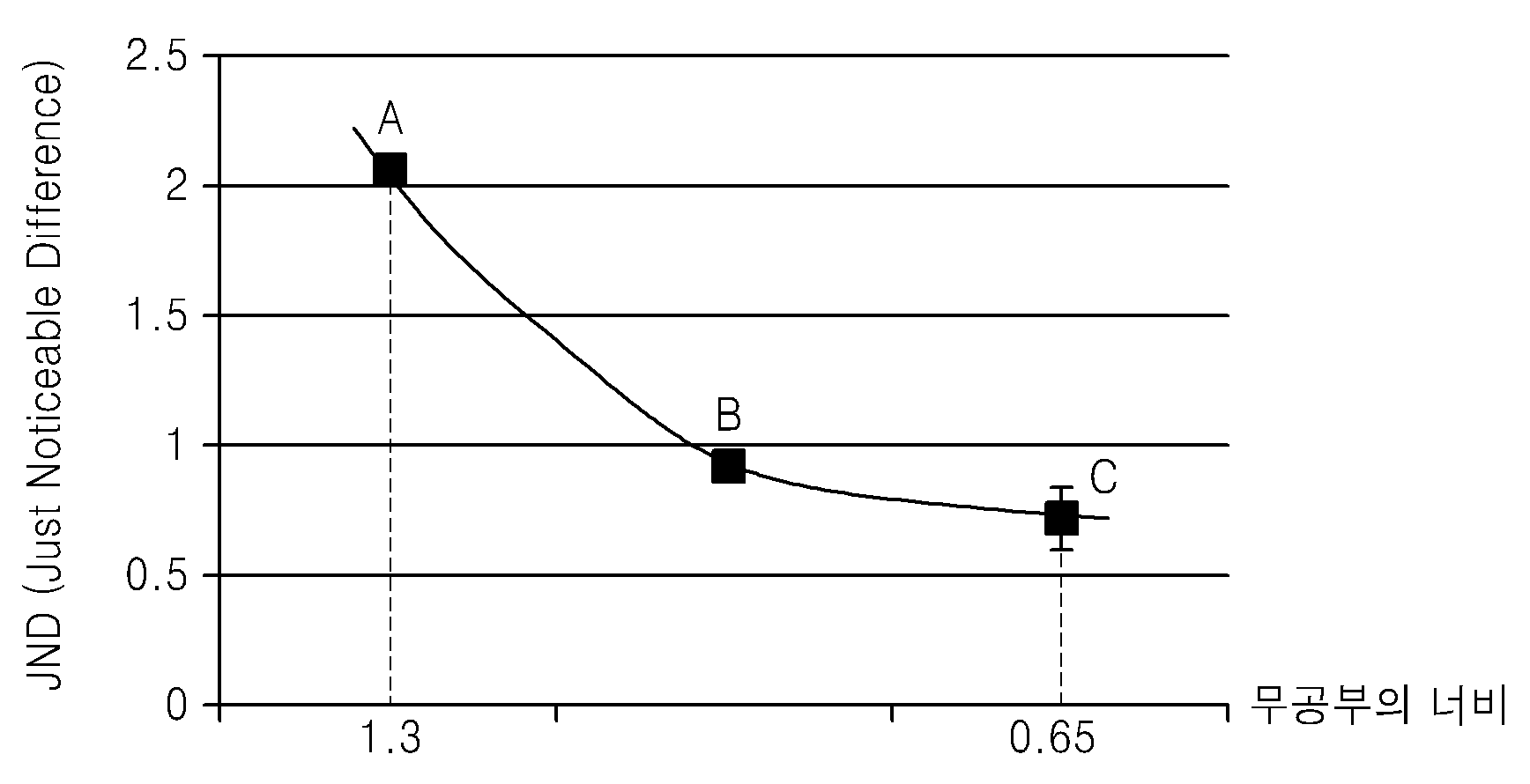
이하, 리브(134)의 폭(W)과 증착 정확도(pixel per accuracy, PPA) 및 기판(600)에 증착되는 증착 물질의 막 균일도와의 관계를 설명하고, 증착 물질의 막 균일도가 유기 디스플레이 장치의 품질에 미치는 영향에 대해서 설명하기로 한다. 여기에서, 증착 정확도, 즉 PPA라 함은 증착 물질이 기판(600) 상에 설계한 바대로 정확하게 증착되었는지 여부를 나타내는 하나의 지표로서, 증착 정확도를 판단하는 하나의 기준이다.The relationship between the width W of the
패터닝 슬릿 시트(130)는 Y축 방향으로 인장력이 가해진 채로 프레임(135)과 결합한다. 이는 패터닝 슬릿 시트(130)를 최대한 평탄하게 배치함으로써, 증착 공정 시 기판에 음영(shadow) 영역이 증착되지 않도록 하기 위함이다.The
하지만, 패터닝 슬릿 시트(130)의 강성이 충분히 확보되지 않은 경우에는 Y축 방향의 인장에 의해 패터닝 슬릿 시트(130)의 패터닝 슬릿(131)의 형상에 변형이 일어날 수 있다. 이렇게 패터닝 슬릿(131)에 변형이 일어나게 될 경우에는, 증착 정확도가 저하될 수 있다.However, if the rigidity of the
따라서, 증착 정확도를 저하시키지 않기 위해서는 Y축 방향의 인장력에 의한 패터닝 슬릿(131)의 변형을 최소화할 필요성이 있다.Therefore, in order not to lower the deposition accuracy, it is necessary to minimize the deformation of the patterning slit 131 due to the tensile force in the Y-axis direction.
리브(134)는 패터닝 슬릿(131)에 Y축 방향으로 연장되도록 형성되는 복수개의 개구부(133)들 사이에 X축 방향으로 연장되도록 형성되어, Y축을 따라 복수개가 이격되어 형성되는 각 개구부(133)를 구분한다.The
이러한 리브(134)가 각 개구부(133)들 사이에 많이 존재할수록, 그리고 리브(134)의 폭(W)이 넓을 수록 Y축 방향으로 강건 인장이 가능하며, 이에 따라 패터닝 슬릿(131)의 변형 또한 감소시킬 수 있다. 결과적으로, 강건 인장된 상태에서 프레임(135)에 결합되는 패터닝 슬릿 시트(130)로 증착 물질을 기판(600)에 증착하게 되면 증착 정확도를 향상시킬 수 있다.The greater the widths W of the
하지만, 리브(134)의 개수를 늘리거나 리브(134)의 폭(W)을 적정한 수준 이상으로 넓히게 되면, 기판(600)에 증착 물질이 불균일하게 증착되는 문제점이 발생한다. 이렇게 증착 물질이 기판(600)에 불균일하게 증착되면, 증착 공정 완료 후 유기 발광 디스플레이 장치의 점등 시 유기 발광 디스플레이 장치의 패널이 얼룩져 보이는 현상이 발생한다.However, if the number of the
이러한 얼룩 현상을 개선하기 위해서는, 증착 정확도를 개선하는 방법과 반대로 리브(134)의 폭을 최대한 줄여 개구부(133)를 통과하는 증착 물질의 양을 늘리는 것이 필요하다. 따라서, PPA와 얼룩 현상을 동시에 개선하기 위해서는, 리브(134)의 폭을 적정 범위로 설계하는 것이 필요하다.In order to improve such a smear phenomenon, it is necessary to increase the amount of the deposition material passing through the
이하 표 1을 참고하면, 리브(134)의 폭(W)이 1.3mm인 경우와 0.65mm인 경우 유기 발광 디스플레이 장치의 시인성(visibility)을 확인할 수가 있다.Referring to Table 1 below, visibility of the organic light emitting display device can be confirmed when the width W of the
[표 1][Table 1]
표 1의 JND(just noticeable difference)는 유기 발광 디스플레이 장치에 발생할 수 있는 다양한 얼룩을 수치화하여 나타낸 값으로, 디스플레이 등에서 얼룩 및 미세멍(mura)의 수준을 파악하는데 사용되며, JND의 수치화를 통해 얼룩이나 미세멍을 최종적으로 보정하는 백데이터로 사용될 수 있다.The JND (just noticeable difference) in Table 1 is a numerical value indicating various types of stains that may occur in the organic light emitting display device. It is used to grasp the level of stains and mura in a display, etc., Or as a back-up data for finally correcting micro-bruises.
여기서, 참조부호 A는 리브(134)의 폭(W)이 1.3mm인 경우를 의미하여, 참조부호 B는 유기 발광 디스플레이 장치의 점등 수준이 양품으로 판정되는 JND값을 나타내며, 참조부호 C는 리브(134)의 폭(W)이 0.65mm인 경우를 나타낸다.Here, A denotes a case where the width W of the
다시 표 1을 참조하면, 리브(134)의 폭(W)이 1.3mm인 경우(B)의 JND 값은 대략 2.05 정도로, 이때 유기 발광 디스플레이 장치의 점등 수준은 불량으로 판정된다. 한편, 리브(134)의 폭(W)이 0.65mm일 경우(C)에는 JND 값은 대략 0.75으로, 유기 발광 디스플레이 장치의 점등 수준이 양품으로 판정되는 JND 값인 0.93(참조부호 B)보다 작으므로 양품으로 판정된다. 이는, 리브(134)의 폭(W)이 0.65mm인 경우에는 디스플레이 패널 상에 발생하는 얼룩이 사람이 인식하지 못할 정도로 시인성(visibility)이 양호하다는 의미이다.Referring back to Table 1, when the width W of the
도 3은 도 1의 유기층 증착 어셈블리(100-1)를 포함하는 증착부(100)를 개략적으로 도시한 사시도이고, 도 4는 도 1의 증착부(100)의 개략적인 단면도이다.FIG. 3 is a perspective view schematically illustrating a
먼저, 도 3 및 도 4를 참조하면, 본 발명의 일 실시예에 관한 유기층 증착 어셈블리(100-1)를 포함하는 유기층 증착 장치(10)의 증착부(100)는 하나 이상의 유기층 증착 어셈블리(100-1)와, 이송부(400)를 포함한다. 3 and 4, a
이하에서는 전체적인 증착부(100)의 구성에 대하여 설명하도록 한다. Hereinafter, the configuration of the entire
챔버(101)는 속이 빈 상자 형상으로 형성되며, 그 내부에 하나 이상의 유기층 증착 어셈블리(100-1)와 이송부(400)가 수용된다. 이를 다른 측면에서 설명하면, 지면에 고정되도록 풋(foot)(102)이 형성되고, 풋(foot)(102) 상에 하부 하우징(103)이 형성되고, 하부 하우징(103)의 상부에 상부 하우징(104)이 형성된다. 그리고, 챔버(101)는 하부 하우징(103) 및 상부 하우징(104)을 모두 내부에 수용하도록 형성된다. 이때 하부 하우징(103)과 챔버(101)의 연결부는 밀봉처리되어 챔버(101) 내부가 외부와 완전히 차단되도록 할 수 있다. 이와 같이 하부 하우징(103)과 상부 하우징(104)이 지면에 고정된 풋(foot)(102) 상에 형성됨으로써, 챔버(101)가 수축/팽창을 반복하더라도 하부 하우징(103)과 상부 하우징(104)은 고정된 위치를 유지할 수 있으며, 따라서 하부 하우징(103)과 상부 하우징(104)이 증착부(100) 내에서 일종의 기준 프레임(reference frame)의 역할을 수행할 수 있는 것이다. The
한편, 상부 하우징(104)의 내부에는 유기층 증착 어셈블리(100-1)와 이송부(400)의 제1 이송부(410)가 형성되고, 하부 하우징(103)의 내부에는 이송부(400)의 제2 이송부(420)가 형성되는 것으로 기술할 수 있다. 그리고, 이동부(430)가 제1 이송부(410)와 제2 이송부(420) 사이를 순환 이동하면서 연속적으로 증착이 수행되는 것이다. The organic layer deposition assembly 100-1 and the
이하에서는 증착부(100) 내에 수용되는 유기층 증착 어셈블리(100-1)의 상세 구성에 대하여 설명한다. Hereinafter, the detailed structure of the organic layer deposition assembly 100-1 accommodated in the
각각의 유기층 증착 어셈블리(100-1)는 증착원(110), 증착원 노즐부(120), 패터닝 슬릿 시트(130), 연결 부재(140), 제1 스테이지(150), 제2 스테이지(160), 카메라(170), 센서(180) 등을 포함한다. 여기서, 도 3 및 도 4의 모든 구성은 적절한 진공도가 유지되는 챔버(101) 내에 배치되는 것이 바람직하다. 이는 증착 물질의 직진성을 확보하기 위함이다. Each organic layer deposition assembly 100-1 includes an
상세히, 증착원(110)에서 방출된 증착 물질(115)이 증착원 노즐부(120) 및 패터닝 슬릿 시트(130)를 통과하여 기판(600)에 원하는 패턴으로 증착되게 하려면, 기본적으로 챔버(101) 내부는 FMM 증착 방법과 동일한 고진공 상태를 유지해야 한다. 또한 패터닝 슬릿 시트(130)의 온도가 증착원(110) 온도보다 충분히 낮아야 한다. 왜냐하면, 패터닝 슬릿 시트(130)의 온도가 충분히 낮아야만 온도에 의한 패터닝 슬릿 시트(130)의 열팽창 문제를 최소화할 수 있기 때문이다. In detail, in order for the
이러한 챔버(101) 내에는 피 증착체인 기판(600)이 배치된다. 상기 기판(600)은 평판 표시장치용 기판이 될 수 있는데, 다수의 평판 표시장치를 형성할 수 있는 마더 글라스(mother glass)와 같은 40인치 이상의 대면적 기판이 적용될 수 있다.In this
여기서, 본 발명의 실시예들에서는, 기판(600)이 유기층 증착 어셈블리(100-1)에 대하여 상대적으로 이동하면서 증착이 진행되는 것을 일 특징으로 한다. Here, in the embodiments of the present invention, the deposition proceeds as the
상세히, 기존 FMM 증착 방법에서는 FMM 크기가 기판 크기와 동일하게 형성되어야 한다. 따라서, 기판 사이즈가 증가할수록 FMM도 대형화되어야 하며, 이로 인해 FMM 제작이 용이하지 않고, FMM을 인장하여 정밀한 패턴으로 얼라인(align) 하기도 용이하지 않다는 문제점이 존재하였다. Specifically, in the conventional FMM deposition method, the FMM size must be formed equal to the substrate size. Therefore, as the substrate size increases, the FMM must be made larger, which makes it difficult to fabricate the FMM, and it is not easy to align the FMM with a precise pattern by pulling the FMM.
이와 같은 문제점을 해결하기 위하여, 본 발명의 일 실시예에 관한 유기층 증착 어셈블리(100-1)는, 유기층 증착 어셈블리(100-1)와 기판(600)이 서로 상대적으로 이동하면서 증착이 이루어지는 것을 일 특징으로 한다. 다시 말하면, 유기층 증착 어셈블리(100-1)와 마주보도록 배치된 기판(600)이 Y축 방향을 따라 이동하면서 연속적으로 증착을 수행하게 된다. 즉, 기판(600)이 도 3의 화살표 A 방향으로 이동하면서 스캐닝(scanning) 방식으로 증착이 수행되는 것이다. 여기서, 도면에는 기판(600)이 챔버(미도시) 내에서 Y축 방향으로 이동하면서 증착이 이루어지는 것으로 도시되어 있으나, 본 발명의 사상은 이에 제한되지 아니하며, 기판(600)은 고정되어 있고 유기층 증착 어셈블리(100-1) 자체가 Y축 방향으로 이동하면서 증착을 수행하는 것도 가능하다 할 것이다. In order to solve such problems, the organic layer deposition assembly 100-1 according to an embodiment of the present invention is configured such that deposition is performed while the organic layer deposition assembly 100-1 and the
따라서, 본 발명의 유기층 증착 어셈블리(100-1)에서는 종래의 FMM에 비하여 훨씬 작게 패터닝 슬릿 시트(130)를 만들 수 있다. 즉, 본 발명의 유기층 증착 어셈블리(100-1)의 경우, 기판(600)이 Y축 방향을 따라 이동하면서 연속적으로, 즉 스캐닝(scanning) 방식으로 증착을 수행하기 때문에, 패터닝 슬릿 시트(130)의 X축 방향 및 Y축 방향의 길이 중 적어도 한 방향의 길이는 기판(600)의 길이보다 훨씬 작게 형성될 수 있는 것이다. Accordingly, the
이와 같이, 종래의 FMM에 비하여 훨씬 작게 패터닝 슬릿 시트(130)를 만들 수 있기 때문에, 본 발명의 패터닝 슬릿 시트(130)는 그 제조가 용이하다. 즉, 패터닝 슬릿 시트(130)의 에칭 작업이나, 그 이후의 정밀 인장 및 용접 작업, 이동 및 세정 작업 등 모든 공정에서, 작은 크기의 패터닝 슬릿 시트(130)가 FMM 증착 방법에 비해 유리하다. 또한, 이는 디스플레이 장치가 대형화될수록 더욱 유리하게 된다.As described above, since the
이와 같이, 유기층 증착 어셈블리(100-1)와 기판(600)이 서로 상대적으로 이동하면서 증착이 이루어지기 위해서는, 유기층 증착 어셈블리(100-1)와 기판(600)이 일정 정도 이격되는 것이 바람직하다. 이에 대하여는 뒤에서 상세히 기술하기로 한다. It is preferable that the organic layer deposition assembly 100-1 and the
한편, 챔버 내에서 상기 기판(600)과 대향하는 측에는, 증착 물질(115)이 수납 및 가열되는 증착원(110)이 배치된다. 상기 증착원(110) 내에 수납되어 있는 증착 물질(115)이 기화됨에 따라 기판(600)에 증착이 이루어진다. On the other hand, on the side facing the
상세히, 증착원(110)은 그 내부에 증착 물질(115)이 채워지는 도가니(111)와, 도가니(111)를 가열시켜 도가니(111) 내부에 채워진 증착 물질(115)을 도가니(111)의 일 측, 상세하게는 증착원 노즐부(120) 측으로 증발시키기 위한 히터(112)를 포함한다. In detail, the
증착원(110)의 일 측, 상세하게는 증착원(110)에서 기판(600)을 향하는 측에는 증착원 노즐부(120)가 배치된다. 여기서, 본 발명의 일 실시예에 따른 유기층 증착 어셈블리(100-1)는 공통층과 패턴층을 증착하는데 있어서 증착원 노즐(121)이 서로 상이하게 형성될 수도 있다.The evaporation
즉, 도면에는 도시되지 않았지만, 패턴층을 형성하기 위한 증착원 노즐부(120)에는 Y축 방향 즉 기판(600)의 스캔 방향을 따라서 복수 개의 증착원 노즐(121)들이 형성될 수 있다. 이에 따라, X축 방향으로는 증착원 노즐(121)이 하나만 존재하도록 증착원 노즐(121)을 형성함으로써, 음영(shadow)의 발생을 크게 감소시킬 수 있는 것이다. 반면, 공통층을 형성하기 위한 증착원 노즐부(120)에는 X축 방향을 따라서 복수 개의 증착원 노즐(121)들이 형성될 수 있다. 이에 의해 공통층의 두께 균일도를 향상시킬 수 있는 것이다. That is, although not shown in the drawing, a plurality of
한편, 증착원(110)과 기판(600) 사이에는 패터닝 슬릿 시트(130)가 더 구비된다. 패터닝 슬릿 시트(130)는 대략 창문 틀과 같은 형태로 형성되는 프레임(135)을 더 포함하며, 패터닝 슬릿 시트(130)에는 X축 방향을 따라서 복수 개의 패터닝 슬릿(131)들이 형성된다. 증착원(110) 내에서 기화된 증착 물질(115)은 증착원 노즐부(120) 및 패터닝 슬릿 시트(130)를 통과하여 피 증착체인 기판(600) 쪽으로 향하게 되는 것이다. 이때, 상기 패터닝 슬릿 시트(130)는 종래의 파인 메탈 마스크(FMM) 특히 스트라이프 타입(stripe type)의 마스크의 제조 방법과 동일한 방법인 에칭을 통해 제작될 수 있다. 이때, 증착원 노즐(121)들의 총 개수보다 패터닝 슬릿(131)들의 총 개수가 더 많게 형성될 수도 있다. 패터닝 슬릿 시트(130)에 대한 구체적인 설명은 전술한 바 있으므로, 여기에서는 더 자세한 설명은 생략하도록 한다.A
여기서, 상술한 증착원(110) 및 이와 결합된 증착원 노즐부(120)와 패터닝 슬릿 시트(130)는 서로 일정 정도 이격되도록 형성될 수 있다.The
상술한 바와 같이, 본 발명의 일 실시예에 관한 유기층 증착 어셈블리(100-1)는 기판(600)에 대하여 상대적으로 이동하면서 증착을 수행하며, 이와 같이 유기층 증착 어셈블리(100-1)가 기판(600)에 대하여 상대적으로 이동하기 위해서 패터닝 슬릿 시트(130)는 기판(600)으로부터 일정 정도 이격되도록 형성된다. As described above, the organic layer deposition assembly 100-1 according to one embodiment of the present invention performs deposition while relatively moving relative to the
상세히, 종래의 FMM 증착 방법에서는 기판에 음영(shadow)이 생기지 않도록 하기 위하여 기판에 마스크를 밀착시켜서 증착 공정을 진행하였다. 그러나, 이와 같이 기판에 마스크를 밀착시킬 경우, 기판과 마스크 간의 접촉에 의한 불량 문제가 발생한다는 문제점이 존재하였다. 또한, 마스크를 기판에 대하여 이동시킬 수 없기 때문에, 마스크가 기판과 동일한 크기로 형성되어야 한다. 따라서, 디스플레이 장치가 대형화됨에 따라 마스크의 크기도 커져야 하는데, 이와 같은 대형 마스크를 형성하는 것이 용이하지 아니하다는 문제점이 존재하였다. In detail, in the conventional FMM deposition method, a mask is closely adhered to a substrate to prevent a shadow from being formed on the substrate, and a deposition process is performed. However, when the mask is brought into close contact with the substrate in this manner, there is a problem that a problem of defective due to contact between the substrate and the mask occurs. Further, since the mask can not be moved relative to the substrate, the mask must be formed to have the same size as the substrate. Therefore, as the size of the display device is increased, the size of the mask must be increased. Thus, there is a problem that it is not easy to form such a large mask.
이와 같은 문제점을 해결하기 위하여, 본 발명의 일 실시예에 관한 유기층 증착 어셈블리(100-1)에서는 패터닝 슬릿 시트(130)가 피 증착체인 기판(600)과 소정 간격을 두고 이격되도록 배치되도록 한다. In order to solve such a problem, in the organic layer deposition assembly 100-1 according to an embodiment of the present invention, the
이와 같은 본 발명에 의해서 마스크를 기판보다 작게 형성한 후, 마스크를 기판에 대하여 이동시키면서 증착을 수행할 수 있게 됨으로써, 마스크 제작이 용이해지는 효과를 얻을 수 있다. 또한, 기판과 마스크 간의 접촉에 의한 불량을 방지하는 효과를 얻을 수 있다. 또한, 공정에서 기판과 마스크를 밀착시키는 시간이 불필요해지기 때문에, 제조 속도가 향상되는 효과를 얻을 수 있다. According to the present invention, after the mask is formed smaller than the substrate, the deposition can be performed while moving the mask relative to the substrate, so that it is possible to obtain an effect of facilitating the production of the mask. In addition, it is possible to obtain an effect of preventing defects due to contact between the substrate and the mask. Further, since the time required for the substrate and the mask to adhere to each other in the process becomes unnecessary, an effect of improving the manufacturing speed can be obtained.
다음으로, 상부 하우징(104) 내에서의 각 구성요소의 구체적인 배치는 다음과 같다.Next, the specific arrangement of each component in the
먼저, 상부 하우징(104)의 바닥 부분에는 상술한 증착원(110) 및 증착원 노즐부(120)가 배치된다. 그리고, 증착원(110) 및 증착원 노즐부(120)의 양측에는 안착부(104-1)가 돌출 형성되며, 안착부(104-1) 상에는 제1 스테이지(150), 제2 스테이지(160) 및 상술한 패터닝 슬릿 시트(130)가 차례로 형성된다. First, the
여기서, 제1 스테이지(150)는 X축 방향 및 Y축 방향으로 이동 가능하도록 형성되어, 패터닝 슬릿 시트(130)를 X축 방향 및 Y축 방향으로 얼라인 하는 기능을 수행한다. 즉, 제1 스테이지(150)는 복수 개의 액츄에이터를 구비하여, 상부 하우징(104)에 대하여 제1 스테이지(150)가 X축 방향 및 Y축 방향으로 이동하도록 형성되는 것이다. Here, the
한편, 제2 스테이지(160)는 Z축 방향으로 이동 가능하도록 형성되어, 패터닝 슬릿 시트(130)를 Z축 방향으로 얼라인 하는 기능을 수행한다. 즉, 제2 스테이지(160)는 복수 개의 액츄에이터를 구비하여, 제1 스테이지(150)에 대하여 제2 스테이지(160)가 Z축 방향으로 이동하도록 형성되는 것이다. Meanwhile, the
한편, 제2 스테이지(160) 상에는 패터닝 슬릿 시트(130)가 형성된다. 이와 같이, 패터닝 슬릿 시트(130)가 제1 스테이지(150) 및 제2 스테이지(160) 상에 형성되어 패터닝 슬릿 시트(130)가 X축 방향, Y축 방향 및 Z축 방향으로 이동 가능하도록 형성됨으로써, 기판(600)과 패터닝 슬릿 시트(130) 간의 얼라인, 특히 리얼타임 얼라인(real-time align)을 수행할 수 있는 것이다. On the other hand, a
나아가 상부 하우징(104), 제1 스테이지(150) 및 제2 스테이지(160)는 증착원 노즐(121)을 통해 배출되는 증착 물질이 분산되지 않도록 증착 물질의 이동 경로를 가이드 하는 역할을 동시에 수행할 수 있다. 즉, 상부 하우징(104), 제1 스테이지(150) 및 제2 스테이지(160)에 의해 증착 물질의 경로가 밀폐되어 증착 물질의 X축 방향 및 Y축 방향 이동을 동시에 가이드 할 수도 있다. Further, the
한편, 패터닝 슬릿 시트(130)와 증착원(110) 사이에는 연결 부재(140)가 더 구비될 수도 있다. 상세히, 기판(600)의 테두리 부분에는 애노드 전극 또는 캐소드 전극 패턴이 형성되어, 향후 제품 검사용 또는 제품 제작시 단자로 활용하기 위한 영역이 존재한다. 만약 이 영역에 유기물이 성막이 될 경우, 애노드 전극 또는 캐소드 전극이 제 역할을 하기 어렵데 되며, 따라서 이와 같은 기판(600)의 테두리 부분은 유기물 등이 성막되지 않아야 하는 비성막 영역이 되어야 한다. 그러나 상술한 바와 같이, 본 발명의 박막 증착 장치에서는 기판(600)이 박막 증착 장치에 대하여 이동하면서 스캐닝(scanning) 방식으로 증착이 수행되므로, 기판(600)의 비성막 영역에 유기물 증착을 방지하는 것이 용이하지 않았다. The
이와 같이 기판(600)의 비성막 영역에 유기물이 증착되는 것을 방지하기 위하여, 본 발명의 일 실시예에 관한 박막 증착 장치에서는 기판(600)의 테두리 부분에 별도의 연결 부재(140)가 더 구비될 수 있다. 도면에는 상세히 도시되지 않았지만, 연결 부재(140)는 서로 이웃한 두 개의 플레이트로 구성될 수 있다. In order to prevent organic substances from being deposited on the non-deposition region of the
기판(600)이 유기층 증착 어셈블리(100-1)를 통과하지 아니할 때에는, 연결 부재(140)가 증착원(110)을 가림으로써, 증착원(110)에서 발산된 증착 물질(115)이 패터닝 슬릿 시트(130)에 묻지 않도록 한다. 이 상태에서 기판(600)이 유기층 증착 어셈블리(100-1)로 진입하기 시작하면, 증착원(110)을 가리고 있던 전방의 연결 부재(140)가 기판(600)의 이동과 함께 이동하면서 증착 물질의 이동 경로가 오픈되어, 증착원(110)에서 발산된 증착 물질(115)이 패터닝 슬릿 시트(130)를 통과하여 기판(600)에 증착된다.When the
한편, 기판(600) 전체가 유기층 증착 어셈블리(100-1)를 통과하면, 후방의 연결 부재(140)가 기판(600)의 이동과 함께 이동하면서 증착 물질의 이동 경로를 다시 폐쇄하여 증착원(110)을 가림으로써, 증착원(110)에서 발산된 증착 물질(115)이 패터닝 슬릿 시트(130)에 묻지 않도록 한다. When the
이와 같은 연결 부재(140)에 의해서 기판(600)의 비성막 영역이 가려짐으로써, 별도의 구조물 없이도 간편하게 기판(600)의 비성막 영역에 유기물이 증착되는 것이 방지되는 효과를 얻을 수 있다. The non-deposition region of the
이하에서는 피증착체인 기판(600)을 이송하는 이송부(400)에 대하여 상세히 설명하도록 한다. 도 3 및 도 4를 참조하면, 이송부(400)는 제1 이송부(410)와, 제2 이송부(420)와, 이동부(430)를 포함한다. Hereinafter, the
제1 이송부(410)는 유기층 증착 어셈블리(100-1)에 의해 기판(600) 상에 유기층이 증착될 수 있도록, 캐리어(431) 및 이와 결합된 정전 척(432)을 포함하는 이동부(430)와, 이동부(430)에 부착되어 있는 기판(600)을 인라인(in-line)으로 이송하는 역할을 수행한다. 이와 같은 제1 이송부(410)는 코일(411), 가이드부(412), 상면 자기부상 베어링(미도시), 측면 자기부상 베어링(미도시), 갭 센서(미도시)를 포함한다. The
제2 이송부(420)는 증착부(100)를 통과하면서 1회의 증착이 완료된 후 언로딩부(300)에서 기판(600)이 분리된 이동부(430)를 로딩부(200)로 회송하는 역할을 수행한다. 이와 같은 제2 이송부(420)는 코일(421), 롤러 가이드(422) 및 차징 트랙(charging track)(423)을 포함한다. The
이동부(430)는 제1 이송부(410) 및 제2 이송부(420)를 따라 이송되는 캐리어(431)와, 캐리어(431)의 일 면상에 결합되며 기판(600)이 부착되는 정전 척(432)을 포함한다. The moving
이하에서는 이송부(400)의 각 구성요소에 대하여 더욱 상세히 설명한다. Hereinafter, each component of the
먼저, 이동부(430)의 캐리어(431)에 대해 상세히 설명한다. First, the
캐리어(431)는 본체부(431a), 마그네틱 레일(431b), CPS 모듈(Contactless power supply Module)(431c), 전원부(431d) 및 가이드 홈(431e)을 포함한다. The
본체부(431a)는 캐리어(431)의 기저부를 이루며, 철과 같은 자성체로 형성될 수 있다. 이와 같은 캐리어(431)의 본체부(431a)와 후술할 자기부상 베어링(미도시)과의 척력에 의하여 캐리어(431)가 가이드부(412)에 대해 일정 정도 이격된 상태를 유지할 수 있다. The
본체부(431a)의 양측면에는 가이드 홈(431e)이 형성될 수 있으며, 이와 같은 가이드 홈(431e) 내에는 가이드부(412)의 가이드 돌기(412e)가 수용될 수 있다.
본체부(431a)의 진행방향의 중심선을 따라 마그네틱 레일(431b)이 형성될 수 있다. 본체부(431a)의 마그네틱 레일(431b)과 후술할 코일(411)이 결합하여 리니어 모터를 구성할 수 있으며, 이와 같은 리니어 모터에 의하여 캐리어(431)가 A방향으로 이송될 수 있는 것이다. A
본체부(431a)에서 마그네틱 레일(431b)의 일 측에는 CPS 모듈(431c) 및 전원부(431d)가 각각 형성될 수 있다. 전원부(431d)는 정전 척(432)이 기판(600)을 척킹(chucking)하고 이를 유지할 수 있도록 전원을 제공하기 위한 일종의 충전용 배터리이며, CPS 모듈(431c)은 전원부(431d)를 충전하기 위한 무선 충전 모듈이다.A
상세히, 후술할 제2 이송부(420)에 형성된 차징 트랙(charging track)(423)은 인버터(inverter)(미도시)와 연결되어, 캐리어(431)가 제2 이송부(420) 내에서 이송될 때, 차징 트랙(charging track)(423)과 CPS 모듈(431c) 사이에 자기장이 형성되어 CPS 모듈(431c)에 전력을 공급한다. 그리고, CPS 모듈(431c)에 공급된 전력은 전원부(431d)를 충전하게 되는 것이다.In detail, a charging
한편, 정전척(Electro Static Chuck, 432)은 세라믹으로 구비된 본체의 내부에 전원이 인가되는 전극이 매립된 것으로, 이 전극에 고전압이 인가됨으로써 본체의 표면에 기판(600)을 부착시키는 것이다. The
다음으로, 이동부(430)의 구동에 대해 상세히 설명한다. Next, the driving of the moving
본체부(431a)의 마그네틱 레일(431b)과 코일(411)이 결합하여 구동부를 구성할 수 있다. 여기서, 구동부는 리니어 모터(Linear Motor)일 수 있다. 리니어 모터는 종래의 미끄럼 안내 시스템에 비하여 마찰 계수가 작고 위치 오차가 거의 발생하지 않아 위치 결정도가 매우 높은 장치이다. 상술한 바와 같이, 리니어 모터는 코일(411)과 마그네틱 레일(431b)로 이루어질 수 있으며, 마그네틱 레일(431b)이 캐리어(431) 상에 일렬로 배치되고, 코일(411)은 마그네틱 레일(431b)과 마주보도록 챔버(101) 내의 일 측에 다수 개가 일정 간격으로 배치될 수 있다. 이와 같이 이동 물체인 캐리어(431)에 코일(411)이 아닌 마그네틱 레일(431b)이 배치되므로 캐리어(431)에 전원을 인가하지 않아도 캐리어(431)의 구동이 가능해질 수 있다. 여기서, 코일(411)은 ATM 상자(atmosphere box) 내에 형성되어 대기 상태에 설치되고, 마그네틱 레일(431b)은 캐리어(431)에 부착되어 진공인 챔버(101) 내에서 캐리어(431)가 주행할 수 있게 되는 것이다. The
다음으로, 제1 이송부(410) 및 이동부(430)에 대해 상세히 설명한다. Next, the
도 4를 참조하면, 제1 이송부(410)는 기판(600)을 고정하고 있는 정전 척(432) 및 이를 이송하는 캐리어(431)를 이동시키는 역할을 수행한다. 여기서, 제1 이송부(410)는 코일(411), 가이드부(412), 상면 자기부상 베어링(미도시), 측면 자기부상 베어링(미도시), 갭 센서(미도시)를 포함한다. Referring to FIG. 4, the
코일(411)과 가이드부(412)는 각각 상부 하우징(104)의 내부면에 형성되며, 이중 코일(411)은 상부 하우징(104)의 상측 내부면에 형성되고, 가이드부(412)는 상부 하우징(104)의 양측 내부면에 형성된다. The
가이드부(412)는 캐리어(431)가 일 방향으로 이동되도록 가이드하는 역할을 수행한다. 이때, 가이드부(412)는 증착부(100)를 관통하도록 형성된다. The
측면 자기부상 베어링(미도시)은 캐리어(431)의 양 측면에 대응되도록 가이드부(412) 내에 각각 배치된다. 측면 자기부상 베어링(미도시)은 캐리어(431)와 가이드부(412) 사이의 간격을 발생시켜, 캐리어(431)가 이동할 때 가이드부(412)와 접촉되지 않고 비접촉 방식으로 가이드부(412)를 따라 이동하도록 하는 역할을 한다. 즉, 좌측의 측면 자기부상 베어링(미도시)과 자성체인 캐리어(431) 사이에 발생하는 척력과, 우측의 측면 자기부상 베어링(미도시)과 자성체인 캐리어(431) 사이에 발생하는 척력이 서로 평형을 이루면서 캐리어(431)와 가이드부(412) 사이의 간격을 발생시키는 동시에 그 간격을 일정하게 유지하는 것이다. Side magnetic levitation bearings (not shown) are respectively disposed in the
한편, 상부 자기부상 베어링(미도시)은 캐리어(431)의 상부에 위치하도록 가이드부(412) 내에 각각 배치된다. 상부 자기부상 베어링(미도시)은 캐리어(431)가 가이드부(412)에 접촉하지 않고 이들과 일정한 간격을 유지하면서 가이드부(412)를 따라 이동하도록 하는 역할을 한다. 즉, 상부 자기부상 베어링(미도시)과 자성체인 캐리어(431) 사이에 발생하는 척력과 중력이 서로 평행을 이루면서 캐리어(431)와 가이드부(412) 사이의 간격을 발생시키는 동시에 그 간격을 일정하게 유지하는 것이다. On the other hand, the upper magnetic levitation bearings (not shown) are respectively disposed in the
가이드부(412)는 갭 센서(미도시)를 더 구비할 수 있다. 갭 센서(미도시)는 캐리어(431)와 가이드부(412) 사이의 간격을 측정할 수 있다. 또한, 측면 자기부상 베어링(미도시)의 일 측에도 갭 센서(미도시)가 배치될 수 있다. 측면 자기부상 베어링(미도시)에 배치된 갭 센서(미도시)는 캐리어(431)의 측면과 측면 자기부상 베어링(미도시) 사이의 간격을 측정할 수 있다.The
갭 센서(미도시)에 의해 측정된 값에 따라 자기부상 베어링(미도시)의 자기력이 변경되어 캐리어(431)와 가이드부(412) 사이의 간격이 실시간으로 조절될 수 있다. 즉, 자기부상 베어링(미도시)과 갭 센서(미도시)를 이용한 피드백 제어에 의해 캐리어(431)의 정밀 이동이 가능하다.The magnetic force of the magnetic levitation bearing (not shown) is changed according to the value measured by the gap sensor (not shown), so that the interval between the
다음으로, 제2 이송부(420) 및 이동부(430)에 대해 상세히 설명한다. Next, the
다시 도 4를 참조하면, 제2 이송부(420)는 언로딩부(300)에서 기판이 분리되고 난 이후의 정전 척(432) 및 이를 이송하는 캐리어(431)를 다시 로딩부(200)로 이동시키는 역할을 수행한다. 여기서, 제2 이송부(420)는 코일(421), 롤러 가이드(422), 차징 트랙(charging track)(423)을 포함한다. 4, the
상세히, 코일(421), 롤러 가이드(422) 및 차징 트랙(423)은 각각 하부 하우징(103)의 내부면에 형성되며, 이중 코일(421)과 차징 트랙(423)은 하부 하우징(103)의 상측 내부면에 형성되고, 롤러 가이드(422)는 하부 하우징(103)의 양측 내부면에 형성된다. 여기서, 코일(421)은 제1 이송부(410)의 코일(411)과 마찬가지로 ATM 상자(atmosphere box) 내에 형성될 수 있다. In detail, the
한편, 제1 이송부(410)와 마찬가지로 제2 이송부(420) 역시 코일(421)을 구비하며, 캐리어(431)의 본체부(431a)의 마그네틱 레일(431b)과 코일(421)이 결합하여 구동부를 구성할 수 있으며, 여기서 구동부는 리니어 모터(Linear Motor)일 수 있다. 이와 같은 리니어 모터(Linear Motor)에 의해서 캐리어(431)가 도 3의 A방향의 반대 방향을 따라 이동할 수 있다. Similarly to the
한편, 롤러 가이드(422)는 캐리어(431)가 일 방향으로 이동되도록 가이드하는 역할을 수행한다. 이때, 롤러 가이드(422)는 증착부(100)를 관통하여 형성된다. Meanwhile, the
결과적으로, 제2 이송부(420)는 기판에 유기물을 증착하는 단계가 아닌, 비어있는 캐리어(431)를 회송하는 단계이기 때문에, 제1 이송부(410)에 비해 위치 정밀도가 크게 요구되지 아니한다. 따라서, 높은 위치 정밀도가 요구되는 제1 이송부(410)에는 자기 부상을 적용하여 위치 정밀도를 확보하고, 상대적으로 낮은 위치 정밀도가 요구되는 제2 이송부(420)에는 종래의 롤러 방식을 적용하여 제조 단가를 낮추고 유기층 증착 장치의 구성을 간결하게 하는 것이다. 물론, 도면에는 도시되지 않았지만, 제2 이송부(420)에도 제1 이송부(410)와 마찬가지로 자기 부상을 적용하는 것도 가능하다 할 것이다. As a result, the position of the
한편, 본 발명의 일 실시예에 따른 유기층 증착 장치(1)의 유기층 증착 어셈블리(100-1)는 얼라인(align)을 위한 카메라(170) 및 센서(180)를 더 구비할 수 있다. 상세히, 카메라(170)는 패터닝 슬릿 시트(130)의 프레임(135)에 형성된 제 1마크(미도시)와 기판(600)에 형성된 제2 마크(미도시)를 실시간으로 얼라인할 수 있다. 여기서, 카메라(170)는 증착이 진행중인 진공 챔버(101) 내에서 원활한 시야 확보를 할 수 있도록 구비된다. 이를 위해, 카메라(170)는 카메라 수용부(171) 내에 형성되어 대기 상태에 설치될 수 있다.The organic layer deposition assembly 100-1 of the organic layer deposition apparatus 1 according to an embodiment of the present invention may further include a
한편, 본 발명에서는 기판(600)과 패터닝 슬릿 시트(130)가 일정 정도 이격되어 있는바, 하나의 카메라(170)를 이용하여, 서로 다른 위치에 있는 기판(600)까지의 거리와 패터닝 슬릿 시트(130)까지의 거리를 함께 측정하여야 한다. 이를 위해, 본 발명의 일 실시예에 따른 유기층 증착 장치(10)의 유기층 증착 어셈블리(100-1)는 센서(180)를 구비할 수 있다. 여기서, 센서(180)는 공초점 센서(Confocal sensor)일 수 있다. 공초점 센서는 고속으로 회전하는 스캐닝 미러(scanning mirror)를 이용하여 레이저 빔으로 측정 대상을 스캐닝하고 레이저 빔에 의해 발광된 형광 또는 반사광선을 이용하여 측정대상까지의 거리를 측정할 수 있다. 공초점 센서는 서로 다른 매질 사이의 경계면을 감지하여 거리를 측정할 수 있다.In the present invention, since the
이와 같이 카메라(170) 및 센서(180)를 구비하여, 실시간으로 기판(600)과 패터닝 슬릿 시트(130) 간의 간격을 측정하는 것이 가능해지고 따라서 실시간으로 기판(600)과 패터닝 슬릿 시트(130)를 얼라인 하는 것이 가능해짐으로써, 패턴의 위치 정밀도가 더욱 향상되는 효과를 얻을 수 있다.It is possible to measure the interval between the
도 5는 도 4의 증착부를 포함하는 유기층 증착 장치(10)를 개략적으로 도시한 시스템 구성의 평면도이고, 도 6은 도 5의 유기층 증착 장치(10)의 증착부(100)를 개략적으로 도시한 시스템 구성의 측면도이다.FIG. 5 is a plan view of a system configuration schematically showing an organic
도 5 및 도 6을 참조하면, 유기층 증착 장치(10)는 본 발명의 일 실시예에 따른 유기층 증착 어셈블리(100-n)(n은 1 이상의 자연수)를 포함하는 증착부(100)와, 로딩부(200), 언로딩부(300) 및 이송부(400)를 포함한다.5 and 6, the organic
로딩부(200)는 제1 랙(Rack)(212)과, 도입실(214)과, 제1 반전실(218)과, 버퍼실(219)을 포함할 수 있다. The
제1 랙(212)에는 증착이 이루어지기 전의 기판(600)이 다수 적재되어 있고, 도입실(214)에 구비된 도입로봇(미도시)은 제1 랙(212)로부터 기판(600)을 잡아 제2 이송부(420)로부터 이송되어 온 이동부(430)에 기판(600)을 얹은 후, 기판(600)이 부착된 이동부(430)를 제1 반전실(218)로 옮긴다. A plurality of
도입실(214)에 인접하게는 제1 반전실(218)이 구비되며, 제1 반전실(218)에 위치한 제1 반전 로봇(미도시)이 이동부(430)를 반전시켜 이동부(430)를 증착부(100)의 제1 이송부(410)에 장착한다. A
도 5에서 볼 때, 도입실(214)의 도입로봇(미도시)은 이동부(430)의 상면에 기판(600)을 얹게 되고, 이 상태에서 이동부(430)는 반전실(218)로 이송되며, 반전실(218)의 제1 반전 로봇(미도시)이 반전실(218)을 반전시킴에 따라 증착부(100)에서는 기판(600)이 아래를 향하도록 위치하게 된다.5, the introduction robot 214 (not shown) of the
언로딩부(300)의 구성은 위에서 설명한 로딩부(200)의 구성과 반대로 구성된다. 즉, 증착부(100)를 거친 기판(600) 및 이동부(430)를 제2 반전실(328)에서 제2 반전 로봇(미도시)이 반전시켜 반출실(324)로 이송하고, 반출 로봇이 반출실(324)에서 기판(600) 및 이동부(430)를 꺼낸 다음, 기판(600)을 이동부(430)에서 분리하여 제2 랙(Rack)(322)에 적재한다. 기판(600)과 분리된 이동부(430)는 제2 이송부(420)를 통해 로딩부(200)로 회송된다.The configuration of the
그러나, 본 발명의 실시예들은 반드시 이에 한정되는 것은 아니며, 기판(600)이 이동부(430)에 최초 고정될 때부터 이동부(430)의 하면에 기판(600)을 고정시켜 그대로 증착부(100)로 이송시킬 수도 있다. 이 경우, 예컨대 제1 반전실(218)의 제1 반전 로봇(미도시)과 제2 반전실(328)의 제2 반전 로봇(미도시)은 필요없게 된다.However, the present invention is not limited thereto. The
증착부(100)는 적어도 하나의 증착용 챔버(101)를 구비한다. 도 5 및 도 6를 참고하면, 상기 증착부(100)는 챔버(101)를 구비하며, 이 챔버(101) 내에 복수의 유기층 증착 어셈블리들(100-1)(100-2)...(100-n)이 배치된다. 상세히, 도 5를 참조하면, 상기 챔버(101) 내에 제1 유기층 증착 어셈블리(100-1), 제2 유기층 증착 어셈블리(100-2) ~ 제11 유기층 증착 어셈블리(100-11)의 열한 개의 유기층 증착 어셈블리들이 설치되어 있으나, 그 숫자는 증착 물질 및 증착 조건에 따라 가변 가능하다. 상기 챔버(101)는 증착이 진행되는 동안 진공으로 유지된다. The
한편, 상기 기판(600)이 고정된 이동부(430)는 제1 이송부(410)에 의해 적어도 증착부(100)로, 바람직하게는 상기 로딩부(200), 증착부(100) 및 언로딩부(300)로 순차 이동되고, 상기 언로딩부(300)에서 기판(600)과 분리된 이동부(430)는 제2 이송부(420)에 의해 로딩부(200)로 환송된다.The moving
상기 제1 이송부(410)는 상기 증착부(100)를 통과할 때에 상기 챔버(101)를 관통하도록 구비되고, 상기 제2 이송부(420)는 기판(600)이 분리된 이동부(430)를 이송하도록 구비된다.The
여기서, 유기층 증착 장치(10)는 제1 이송부(410)와 제2 이송부(420)가 상하로 형성되어, 제1 이송부(410)를 통과하면서 증착을 마친 이동부(430)가 언로딩부(300)에서 기판(600)과 분리된 후, 그 하부에 형성된 제2 이송부(420)를 통해 로딩부(200)로 회송되도록 형성됨으로써, 공간 활용의 효율이 향상되는 효과를 얻을 수 있다. In the organic
한편, 도 5의 증착부(100)는 각 유기층 증착 어셈블리(100-n)(n은 1 이상의 자연수)의 일 측에 증착원 교체부(190)를 더 포함할 수 있다. 도면에는 자세히 도시되지 않았지만, 증착원 교체부(190)는 카세트 형식으로 형성되어, 각각의 유기층 증착 어셈블리(100-n(n은 1 이상의 자연수)로부터 외부로 인출되도록 형성될 수 있다. 따라서, 유기층 증착 어셈블리(100-n(n은 1 이상의 자연수)의 증착원(도 4의 참조부호 110 참조)의 교체가 용이해질 수 있다.5 may further include an evaporation
한편, 도 5에는 로딩부(200), 증착부(100), 언로딩부(300) 및 이송부(400)로 구성된 유기층 증착 장치를 구성하기 위한 일련의 세트(set)가 나란히 두 세트가 구비된 것으로 도시되어 있다. 즉, 도 5의 위쪽과 아래쪽에 총 두 개의 유기층 증착 장치(10)가 구비된 것으로 이해할 수 있다. 이 경우, 두 개의 유기층 증착 장치(10) 사이에는 패터닝 슬릿 시트 교체부(500)가 더 구비될 수 있다.5 shows a set of a set for constituting an organic layer deposition apparatus composed of a
즉, 두 개의 유기층 증착 장치(10) 사이에 패터닝 슬릿 시트 교체부(500)를 구비하여, 두 개의 유기층 증착 장치(10)가 패터닝 슬릿 시트 교체부(500)를 공동으로 사용하도록 함으로써, 각각의 유기층 증착 장치(10)가 패터닝 슬릿 시트 교체부(500)를 구비하는 것에 비하여 공간 활용의 효율성을 향상시킬 수 있는 것이다.That is, the patterning slit
도 7은 도 5의 유기층 증착 장치(10)를 이용하여 제조된 액티브 매트릭스형 유기 발광 디스플레이 장치의 단면을 도시한 것이다.7 is a cross-sectional view of an active matrix organic light emitting display device manufactured using the organic
도 7을 참조하면, 상기 액티브 매트리스형의 유기 발광 디스플레이 장치는 기판(600) 상에 형성된다. 상기 기판(600)은 투명한 소재, 예컨대 글래스재, 플라스틱재, 또는 금속재로 형성될 수 있다. 상기 기판(600)상에는 전체적으로 버퍼층과 같은 절연막(51)이 형성되어 있다. Referring to FIG. 7, the active matrix type organic light emitting display device is formed on a
상기 절연막(51) 상에는 도 7에서 볼 수 있는 바와 같은 TFT와, 유기 발광 소자(OLED)가 형성된다.On the insulating layer 51, a TFT as shown in FIG. 7 and an organic light emitting diode (OLED) are formed.
상기 절연막(51)의 윗면에는 소정 패턴으로 배열된 반도체 활성층(52)이 형성되어 있다. 상기 반도체 활성층(52)은 게이트 절연막(53)에 의하여 매립되어 있다. 상기 활성층(52)은 p형 또는 n형의 반도체로 구비될 수 있다.On the upper surface of the insulating film 51, a semiconductor
상기 게이트 절연막(53)의 윗면에는 상기 활성층(52)과 대응되는 곳에 TFT의 게이트 전극(54)이 형성된다. 그리고, 상기 게이트 전극(54)을 덮도록 층간 절연막(55)이 형성된다. 상기 층간 절연막(55)이 형성된 다음에는 드라이 에칭 등의 식각 공정에 의하여 상기 게이트 절연막(53)과 층간 절연막(55)을 식각하여 콘택 홀을 형성시켜서, 상기 활성층(52)의 일부를 드러나게 한다. A
그 다음으로, 상기 층간 절연막(55) 상에 소스/드레인 전극(56, 57)이 형성되는 데, 콘택 홀을 통해 노출된 활성층(52)에 접촉되도록 형성된다. 상기 소스/드레인 전극(56, 57)을 덮도록 보호막(58)이 형성되고, 식각 공정을 통하여 상기 드레인 전극(57)의 일부가 드러나도록 한다. 상기 보호막(58) 위로는 보호막(58)의 평탄화를 위해 별도의 절연막(59)을 더 형성할 수도 있다.Next, source /
한편, 상기 유기 발광 소자(OLED)는 전류의 흐름에 따라 적,녹,청색의 빛을 발광하여 소정의 화상 정보를 표시하기 위한 것으로서, 상기 보호막(58) 상에 제1 전극(61)을 형성한다. 상기 제1 전극(61)은 TFT의 드레인 전극(57)과 전기적으로 연결된다. The organic light emitting diode OLED emits red, green, and blue light according to the current flow to display predetermined image information. The organic light emitting diode OLED has a
그리고, 상기 제1 전극(61)을 덮도록 화소 정의막(60)이 형성된다. 이 화소 정의막(60)에 소정의 개구를 형성한 후, 이 개구로 한정된 영역 내에 발광층을 포함하는 유기층(62)을 형성한다. 그리고 유기층(62) 위로는 제2 전극(63)을 형성한다.The
상기 화소 정의막(60)은 각 화소를 구획하는 것으로, 유기물로 형성되어, 제1 전극(61)이 형성되어 있는 기판의 표면, 특히, 절연막(59)의 표면을 평탄화한다.The
상기 제1 전극(61)과 제2 전극(63)은 서로 절연되어 있으며, 발광층을 포함하는 유기층(62)에 서로 다른 극성의 전압을 가해 발광이 이뤄지도록 한다.The
상기 발광층을 포함하는 유기층(62)은 저분자 또는 고분자 유기물이 사용될 수 있는 데, 저분자 유기물을 사용할 경우 정공 주입층(HIL: Hole Injection Layer), 정공 수송층(HTL: Hole Transport Layer), 발광층(EML: Emission Layer), 전자 수송층(ETL: Electron Transport Layer), 전자 주입층(EIL: Electron Injection Layer) 등이 단일 혹은 복합의 구조로 적층되어 형성될 수 있으며, 사용 가능한 유기 재료도 구리 프탈로시아닌(CuPc: copper phthalocyanine), N,N-디(나프탈렌-1-일)-N,N'-디페닐-벤지딘 (N,N'-Di(naphthalene-1-yl)-N,N'-diphenyl-benzidine: NPB) , 트리스-8-하이드록시퀴놀린 알루미늄(tris-8-hydroxyquinoline aluminum)(Alq3) 등을 비롯해 다양하게 적용 가능하다. When a low-molecular organic material is used, a hole injection layer (HIL), a hole transport layer (HTL), a light emitting layer (EML), and a light emitting layer (EML) may be used as the
여기서, 상기 발광층을 포함하는 유기층(62)은 도 5에 도시된 유기층 증착 장치(도 5의 참조부호 10 참조)에 의해서 증착될 수 있다. 즉, 증착 물질을 방사하는 증착원, 증착원의 일 측에 배치되며 복수 개의 증착원 노즐들이 형성되는 증착원 노즐부 및 증착원 노즐부와 대향되게 배치되고 복수 개의 패터닝 슬릿들이 형성되는 패터닝 슬릿 시트를 포함하는 유기층 증착 장치가, 피증착용 기판과 소정 정도 이격되도록 배치된 후, 유기층 증착 장치(도 5의 10 참조)와 기판(도 3의 600 참조) 중 어느 일 측이 타 측에 대하여 상대적으로 이동하면서, 유기층 증착 장치(도 5의 10 참조)에서 방사되는 증착 물질이 기판(도 3의 600 참조)상에 증착되는 것이다. Here, the
이러한 유기 발광막을 형성한 후에는 제2 전극(63)을 역시 동일한 증착 공정으로 형성할 수 있다.After the organic light emitting layer is formed, the
한편, 상기 제1 전극(61)은 애노드 전극의 기능을 하고, 상기 제2 전극(63)은 캐소드 전극의 기능을 할 수 있는 데, 물론, 이들 제1 전극(61)과 제2 전극(63)의 극성은 반대로 되어도 무방하다. 그리고, 제1 전극(61)은 각 화소의 영역에 대응되도록 패터닝될 수 있고, 제2 전극(63)은 모든 화소를 덮도록 형성될 수 있다.The
상기 제1 전극(61)은 투명 전극 또는 반사형 전극으로 구비될 수 있는 데, 투명전극으로 사용될 때에는 ITO, IZO, ZnO, 또는 In2O3로 구비될 수 있고, 반사형 전극으로 사용될 때에는 Ag, Mg, Al, Pt, Pd, Au, Ni, Nd, Ir, Cr, 및 이들의 화합물 등으로 반사층을 형성한 후, 그 위에 ITO, IZO, ZnO, 또는 In2O3로 투명전극층을 형성할 수 있다. 이러한 제1 전극(61)은 스퍼터링 방법 등에 의해 성막된 후, 포토 리소그래피법 등에 의해 패터닝된다.The
한편, 상기 제2 전극(63)도 투명 전극 또는 반사형 전극으로 구비될 수 있는 데, 투명전극으로 사용될 때에는 이 제2 전극(63)이 캐소오드 전극으로 사용되므로, 일함수가 작은 금속 즉, Li, Ca, LiF/Ca, LiF/Al, Al, Ag, Mg, 및 이들의 화합물이 발광층을 포함하는 유기층(62)의 방향을 향하도록 증착한 후, 그 위에 ITO, IZO, ZnO, 또는 In2O3 등으로 보조 전극층이나 버스 전극 라인을 형성할 수 있다. 그리고, 반사형 전극으로 사용될 때에는 위 Li, Ca, LiF/Ca, LiF/Al, Al, Ag, Mg, 및 이들의 화합물을 전면 증착하여 형성한다. 이때, 증착은 전술한 발광층을 포함하는 유기층(62)의 경우와 마찬가지의 방법으로 행할 수 있다.When the
본 발명은 이 외에도, 유기 TFT의 유기층 또는 무기막 등의 증착에도 사용할 수 있으며, 기타, 다양한 소재의 성막 공정에 적용 가능하다.In addition, the present invention can be used for deposition of an organic layer or an inorganic film of an organic TFT, and the present invention is applicable to other various film forming processes.
이와 같이 본 발명은 도면에 도시된 일 실시예를 참고로 하여 설명하였으나 이는 예시적인 것에 불과하며 당해 분야에서 통상의 지식을 가진 자라면 이로부터 다양한 변형 및 실시예의 변형이 가능하다는 점을 이해할 것이다. 따라서, 본 발명의 진정한 기술적 보호 범위는 첨부된 특허청구범위의 기술적 사상에 의하여 정해져야 할 것이다.While the present invention has been particularly shown and described with reference to exemplary embodiments thereof, it is to be understood that the invention is not limited to the exemplary embodiments, and that various changes and modifications may be made therein without departing from the scope of the present invention. Accordingly, the true scope of the present invention should be determined by the technical idea of the appended claims.
10: 유기층 증착 장치 214: 도입실
100: 유기층 증착 어셈블리 218: 제1 반전실
101: 증착용 챔버 300: 언로딩부
110: 증착원 322: 제2 랙
111: 도가니 324: 반출실
112: 히터 328: 제2 반전실
115: 증착물질 400: 이송부
120: 증착원 노즐부 410: 제1 이송부
121: 증착원 노즐 411, 421: 코일
130: 패터닝 슬릿 시트 412: 가이드부
131: 패터닝 슬릿 420: 제2 이송부
132: 스패이서 422: 롤러 가이드
133: 개구부 423: 차징 트랙(charging track)
134: 리브 430: 이동부
135: 프레임 431: 캐리어
140: 연결부재 431a: 본체부
150: 제1 스테이지 431b: 마그네틱 레일
160: 제2 스테이지 431c: CPS 모듈
170: 촬영부재 431d: 전원부
180: 센서 432: 정전척
190: 증착원 교체부 500: 패터닝 슬릿 시트 교체부
200: 로딩부 600: 기판
212: 제1 랙 10: organic layer deposition device 214: introduction chamber
100: organic layer deposition assembly 218: first inversion chamber
101: Evaporation chamber 300: Unloading section
110: evaporation source 322: second rack
111: Crucible 324: Export chamber
112: heater 328: second inversion chamber
115: deposition material 400: transfer part
120: evaporation source nozzle part 410: first conveyance part
121:
130: patterning slit sheet 412: guide part
131: patterning slit 420: second transferring part
132: Spacer 422: Roller guide
133: opening 423: charging track
134: ribs 430:
135: Frame 431: Carrier
140: connecting
150:
160:
170: photographing
180: sensor 432: electrostatic chuck
190: evaporation source replacement part 500: patterning slit sheet replacement part
200: loading part 600: substrate
212: first rack
Claims (20)
상기 증착 물질을 방사하는 증착원;
상기 증착원의 일측에 배치되며, 복수개의 증착원 노즐들이 형성되는 증착원 노즐부;
상기 증착원 노즐부와 대향되게 배치되고, 복수개의 패터닝 슬릿들이 형성되는 패터닝 슬릿 시트;를 포함하고,
상기 기판은 상기 유기층 증착 어셈블리와 소정 정도 이격되도록 형성되어 상기 유기층 증착 어셈블리에 대하여 상대적으로 이동 가능하도록 형성되고,
상기 증착원에서 방사된 상기 증착 물질은 상기 패터닝 슬릿 시트를 통과하여 상기 기판에 패턴을 형성하면서 증착되며,
상기 복수개의 패터닝 슬릿들은,
상기 패터닝 슬릿의 길이 방향으로 연장 형성되며, 상기 패터닝 슬릿의 길이 방향 및 폭 방향으로 복수개가 연속적으로 배치되어 상기 증착 물질을 통과시키는 복수개의 개구부와,
상기 각 개구부들 사이의 상기 패터닝 슬릿의 길이 방향으로 이격된 공간에 형성되는 복수개의 리브를 구비하며,
상기 각 리브들의 폭은 0.65mm인 것을 특징으로 하는, 유기층 증착 어셈블리.An organic layer deposition assembly for depositing a deposition material on a substrate,
An evaporation source for emitting the evaporation material;
An evaporation source nozzle unit disposed at one side of the evaporation source and having a plurality of evaporation source nozzles formed therein;
And a patterning slit sheet disposed opposite to the evaporation source nozzle portion and having a plurality of patterning slits formed therein,
Wherein the substrate is formed to be spaced apart from the organic layer deposition assembly to be relatively movable with respect to the organic layer deposition assembly,
Wherein the deposition material emitted from the evaporation source passes through the patterning slit sheet and is deposited while forming a pattern on the substrate,
Wherein the plurality of patterning slits are arranged in a matrix,
A plurality of openings extending in the longitudinal direction of the patterning slit and continuously arranged in the longitudinal direction and the width direction of the patterning slit to allow the deposition material to pass therethrough;
And a plurality of ribs formed in spaces spaced apart from each other in the longitudinal direction of the patterning slit between the openings,
And the width of each of the ribs is 0.65 mm.
상기 패터닝 슬릿 시트는 상기 패터닝 슬릿 시트의 길이 방향인 제1 방향 및 상기 패터닝 슬릿 시트의 폭 방향인 제2 방향 중 적어도 어느 한 방향에 있어서, 상기 기판보다 작게 형성되는 것을 특징으로 하는, 유기층 증착 어셈블리.The method according to claim 1,
Wherein the patterning slit sheet is formed to be smaller than the substrate in at least one of a first direction which is a longitudinal direction of the patterning slit sheet and a second direction which is a width direction of the patterning slit sheet. .
상기 패터닝 슬릿 시트에는 상기 패터닝 슬릿 시트의 길이 방향인 제1 방향을 따라 상기 복수개의 패터닝 슬릿들이 형성되고,
상기 증착원 노즐부에는 상기 패터닝 슬릿 시트의 폭 방향인 제2 방향을 따라 상기 복수개의 증착원 노즐들이 형성되는 것을 특징으로 하는, 유기층 증착 어셈블리.The method according to claim 1,
Wherein the patterning slit sheet is formed with the plurality of patterning slits along a first direction in a longitudinal direction of the patterning slit sheet,
Wherein the plurality of evaporation source nozzles are formed in the evaporation source nozzle portion along a second direction which is a width direction of the patterning slit sheet.
상기 증착원 및 상기 증착원 노즐부와 상기 패터닝 슬릿 시트는 연결부재에 의해 결합되어 일체로 형성되는 것을 특징으로 하는, 유기층 증착 어셈블리.The method of claim 3,
Wherein the evaporation source, the evaporation source nozzle portion, and the patterning slit sheet are integrally formed by a coupling member.
상기 연결부재는 상기 증착 물질의 이동 경로를 가이드 하는 것을 특징으로 하는, 유기층 증착 어셈블리.5. The method of claim 4,
Wherein the connecting member guides the movement path of the evaporation material.
상기 연결부재는 상기 증착원 및 상기 증착원 노즐부와 상기 패터닝 슬릿 시트 사이의 공간을 외부로부터 밀폐하도록 형성되는 것을 특징으로 하는, 유기층 증착 어셈블리.6. The method of claim 5,
Wherein the connecting member is formed to seal the space between the evaporation source and the evaporation source nozzle portion and the patterning slit sheet from the outside.
상기 이동부에 상기 기판을 고정시키는 로딩부;
진공으로 유지되는 챔버와, 상기 로딩부로부터 이송된 상기 이동부에 고정된 상기 기판에 유기층을 증착하는 하나 이상의 유기층 증착 어셈블리를 포함하는 증착부; 및
상기 증착부를 통과하면서 증착이 완료된 상기 기판을 상기 이동부로부터 분리시키는 언로딩부;를 포함하고,
상기 이동부는 상기 제1 이송부와 상기 제2 이송부 사이를 순환가능하도록 형성되고,
상기 이동부에 고정된 기판은 상기 제1 이송부에 의해 이동되는 동안 상기 유기층 증착 어셈블리와 소정 정도 이격되도록 형성되며,
상기 유기층 증착 어셈블리는,
상기 증착 물질을 방사하는 증착원;
상기 증착원의 일측에 배치되며, 복수개의 증착원 노즐들이 형성되는 증착원 노즐부;
상기 증착원 노즐부와 대향되게 배치되고, 복수개의 패터닝 슬릿들이 형성되는 패터닝 슬릿 시트;를 포함하고,
상기 기판은 상기 유기층 증착 어셈블리와 소정 정도 이격되도록 형성되어 상기 유기층 증착 어셈블리에 대하여 상대적으로 이동 가능하도록 형성되고,
상기 증착원에서 방사된 상기 증착 물질은 상기 패터닝 슬릿 시트를 통과하여 상기 기판에 패턴을 형성하면서 증착되며,
상기 복수개의 패터닝 슬릿들은,
상기 패터닝 슬릿의 길이 방향으로 연장 형성되며, 상기 패터닝 슬릿의 길이 방향 및 폭 방향으로 복수개가 연속적으로 배치되어 상기 증착 물질을 통과시키는 복수개의 개구부와,
상기 각 개구부들 사이의 상기 패터닝 슬릿의 길이 방향으로 이격된 공간에 형성되는 복수개의 리브를 구비하며,
상기 각 리브들의 폭은 0.65mm인 것을 특징으로 하는, 유기층 증착 장치.A moving part formed to be movable with the fixed substrate fixed to the substrate; a first conveying part for moving the moving part in which the substrate is fixed in a first direction; and a second conveying part for moving the moving part, A conveying part including a second conveying part for moving the conveying part in a direction opposite to the first direction;
A loading unit for fixing the substrate to the moving unit;
A deposition unit including a chamber kept in a vacuum state and at least one organic layer deposition assembly for depositing an organic layer on the substrate fixed to the moving part transferred from the loading part; And
And an unloading unit for separating the substrate from the moving unit after the vapor deposition is completed while passing through the vapor deposition unit,
Wherein the moving unit is configured to be circuable between the first transfer unit and the second transfer unit,
Wherein the substrate fixed to the moving unit is spaced apart from the organic layer deposition assembly by a predetermined distance while being moved by the first transfer unit,
The organic layer deposition assembly includes:
An evaporation source for emitting the evaporation material;
An evaporation source nozzle unit disposed at one side of the evaporation source and having a plurality of evaporation source nozzles formed therein;
And a patterning slit sheet disposed opposite to the evaporation source nozzle portion and having a plurality of patterning slits formed therein,
Wherein the substrate is formed to be spaced apart from the organic layer deposition assembly to be relatively movable with respect to the organic layer deposition assembly,
Wherein the deposition material emitted from the evaporation source passes through the patterning slit sheet and is deposited while forming a pattern on the substrate,
Wherein the plurality of patterning slits are arranged in a matrix,
A plurality of openings extending in the longitudinal direction of the patterning slit and continuously arranged in the longitudinal direction and the width direction of the patterning slit to allow the deposition material to pass therethrough;
And a plurality of ribs formed in spaces spaced apart from each other in the longitudinal direction of the patterning slit between the openings,
And the width of each of the ribs is 0.65 mm.
상기 제1 이송부와 상기 제2 이송부는 상기 증착부를 통과할 때에 상기 증착부를 관통하도록 구비되는 것을 특징으로 하는, 유기층 증착 장치.8. The method of claim 7,
Wherein the first transfer part and the second transfer part are provided so as to pass through the deposition part when passing through the deposition part.
상기 제1 이송부와 상기 제2 이송부는 상하로 나란히 배치되는 것을 특징으로 하는, 유기층 증착 장치.8. The method of claim 7,
Wherein the first transfer unit and the second transfer unit are arranged vertically in parallel.
상기 제1 이송부는 상기 이동부를 상기 로딩부, 증착부 및 언로딩부로 순차 이동시키는 것을 특징으로 하는, 유기층 증착 장치.8. The method of claim 7,
Wherein the first transfer unit sequentially moves the moving unit to the loading unit, the deposition unit, and the unloading unit.
상기 제2 이송부는 상기 이동부를 상기 언로딩부, 증착부 및 로딩부로 순차 이동시시키는 것을 특징으로 하는, 유기층 증착 장치.8. The method of claim 7,
And the second transfer unit sequentially moves the moving unit to the unloading unit, the deposition unit, and the loading unit.
상기 유기층 증착 어셈블리의 상기 패터닝 슬릿 시트는 상기 제1 방향 또는 상기 제2 방향 중 적어도 어느 한 방향에 있어서, 상기 기판보다 작게 형성되는 것을 특징으로 하는, 유기층 증착 장치.8. The method of claim 7,
Wherein the patterning slit sheet of the organic layer deposition assembly is formed to be smaller than the substrate in at least one of the first direction and the second direction.
상기 증착원 노즐부에는 제1 방향을 따라 복수 개의 증착원 노즐들이 형성되고,
상기 패터닝 슬릿 시트에는 상기 제1 방향에 대해 수직인 제2 방향을 따라 복수 개의 패터닝 슬릿들이 형성되는 것을 특징으로 하는, 유기층 증착 장치.8. The method of claim 7,
A plurality of evaporation source nozzles are formed in the evaporation source nozzle portion along a first direction,
Wherein the patterning slit sheet is formed with a plurality of patterning slits along a second direction perpendicular to the first direction.
상기 증착원 및 상기 증착원 노즐부와 상기 패터닝 슬릿 시트는 연결 부재에 의해 결합되어 일체로 형성되는 것을 특징으로 하는, 유기층 증착 장치.14. The method of claim 13,
Wherein the evaporation source, the evaporation source nozzle unit, and the patterning slit sheet are integrally formed by a coupling member.
상기 연결 부재는 상기 증착 물질의 이동 경로를 가이드 하는 것을 특징으로 하는, 유기층 증착 장치. 15. The method of claim 14,
Wherein the connection member guides the movement path of the evaporation material.
상기 연결 부재는 상기 증착원 및 상기 증착원 노즐부와 상기 패터닝 슬릿 시트 사이의 공간을 외부로부터 밀폐하도록 형성되는 것을 특징으로 하는 유기층 증착 장치. 16. The method of claim 15,
Wherein the connection member is formed to seal the space between the evaporation source and the evaporation source nozzle portion and the patterning slit sheet from the outside.
로딩부에서 상기 기판을 이동부에 고정시키는 단계;
상기 기판이 고정된 상기 이동부를, 챔버를 관통하도록 설치된 제1 이송부를 이용하여 상기 챔버 내로 이송하는 단계;
상기 챔버 내에 배치된 유기층 증착 어셈블리와 상기 기판이 소정 정도 이격된 상태에서, 상기 기판이 상기 유기층 증착 어셈블리에 대해 상대적으로 이동하면서 상기 유기층 증착 어셈블리로부터 발산된 증착 물질이 상기 기판에 증착되어 유기층이 형성되는 단계;
언로딩부에서 증착이 완료된 상기 기판을 상기 이동부로부터 분리시키는 단계; 및
상기 기판과 분리된 상기 이동부를, 챔버를 관통하도록 설치된 제2 이송부를 이용하여 상기 로딩부로 이송하는 단계;를 포함하고,
상기 유기층 증착 어셈블리는,
상기 증착 물질을 방사하는 증착원;
상기 증착원의 일측에 배치되며, 복수개의 증착원 노즐들이 형성되는 증착원 노즐부;
상기 증착원 노즐부와 대향되게 배치되고, 복수개의 패터닝 슬릿들이 형성되는 패터닝 슬릿 시트;를 포함하고,
상기 기판은 상기 유기층 증착 어셈블리와 소정 정도 이격되도록 형성되어 상기 유기층 증착 어셈블리에 대하여 상대적으로 이동 가능하도록 형성되고,
상기 증착원에서 방사된 상기 증착 물질은 상기 패터닝 슬릿 시트를 통과하여 상기 기판에 패턴을 형성하면서 증착되며,
상기 복수개의 패터닝 슬릿들은,
상기 패터닝 슬릿의 길이 방향으로 연장 형성되며, 상기 패터닝 슬릿의 길이 방향 및 폭 방향으로 복수개가 연속적으로 배치되어 상기 증착 물질을 통과시키는 복수개의 개구부와,
상기 각 개구부들 사이의 상기 패터닝 슬릿의 길이 방향으로 이격된 공간에 형성되는 복수개의 리브를 구비하며,
상기 각 리브들의 폭은 0.65mm인 것을 특징으로 하는, 유기 발광 디스플레이 장치의 제조 방법.A method of manufacturing an organic light emitting display device using an organic layer deposition apparatus for forming an organic layer on a substrate,
Fixing the substrate to a moving part at a loading part;
Transferring the moving unit to which the substrate is fixed, into the chamber using a first transfer unit provided to penetrate the chamber;
The substrate is moved relative to the organic layer deposition assembly and the deposition material emitted from the organic layer deposition assembly is deposited on the substrate to form an organic layer, with the substrate being spaced a predetermined distance from the organic layer deposition assembly disposed in the chamber ;
Separating the substrate from which the deposition is completed in the unloading portion from the moving portion; And
And transferring the moving unit separated from the substrate to the loading unit using a second transfer unit installed to penetrate the chamber,
The organic layer deposition assembly includes:
An evaporation source for emitting the evaporation material;
An evaporation source nozzle unit disposed at one side of the evaporation source and having a plurality of evaporation source nozzles formed therein;
And a patterning slit sheet disposed opposite to the evaporation source nozzle portion and having a plurality of patterning slits formed therein,
Wherein the substrate is formed to be spaced apart from the organic layer deposition assembly to be relatively movable with respect to the organic layer deposition assembly,
Wherein the deposition material emitted from the evaporation source passes through the patterning slit sheet and is deposited while forming a pattern on the substrate,
Wherein the plurality of patterning slits are arranged in a matrix,
A plurality of openings extending in the longitudinal direction of the patterning slit and continuously arranged in the longitudinal direction and the width direction of the patterning slit to allow the deposition material to pass therethrough;
And a plurality of ribs formed in spaces spaced apart from each other in the longitudinal direction of the patterning slit between the openings,
Wherein the width of each of the ribs is 0.65 mm.
상기 챔버 내부에 복수의 박막 증착 어셈블리들이 구비되어 각 박막 증착 어셈블리들에 의해 상기 기판에 연속적으로 증착이 이루어지는, 유기 발광 디스플레이 장치의 제조 방법.18. The method of claim 17,
Wherein a plurality of thin film deposition assemblies are provided in the chamber, and the thin film deposition assemblies are continuously deposited on the substrate.
상기 이동부는 상기 제1 이송부와 상기 제2 이송부 사이를 순환하는 것을 특징으로 하는, 유기 발광 디스플레이 장치의 제조 방법.18. The method of claim 17,
Wherein the moving part circulates between the first transfer part and the second transfer part.
상기 제1 이송부와 상기 제2 이송부는 상하로 나란히 배치되는 것을 특징으로 하는, 유기 발광 디스플레이 장치의 제조 방법.18. The method of claim 17,
Wherein the first transferring part and the second transferring part are arranged vertically side by side.
Priority Applications (2)
| Application Number | Priority Date | Filing Date | Title |
|---|---|---|---|
| KR1020140178702A KR102291488B1 (en) | 2014-12-11 | 2014-12-11 | Organic layer deposition assembly, apparatus for organic layer deposition comprising the same, and method for manufacturing of organic light emitting display apparatus using the same |
| CN201510368557.5A CN105695935B (en) | 2014-12-11 | 2015-06-29 | Organic layer deposition component, deposition device and method for manufacturing organic light-emitting display device |
Applications Claiming Priority (1)
| Application Number | Priority Date | Filing Date | Title |
|---|---|---|---|
| KR1020140178702A KR102291488B1 (en) | 2014-12-11 | 2014-12-11 | Organic layer deposition assembly, apparatus for organic layer deposition comprising the same, and method for manufacturing of organic light emitting display apparatus using the same |
Publications (2)
| Publication Number | Publication Date |
|---|---|
| KR20160071579A true KR20160071579A (en) | 2016-06-22 |
| KR102291488B1 KR102291488B1 (en) | 2021-08-20 |
Family
ID=56227919
Family Applications (1)
| Application Number | Title | Priority Date | Filing Date |
|---|---|---|---|
| KR1020140178702A Active KR102291488B1 (en) | 2014-12-11 | 2014-12-11 | Organic layer deposition assembly, apparatus for organic layer deposition comprising the same, and method for manufacturing of organic light emitting display apparatus using the same |
Country Status (2)
| Country | Link |
|---|---|
| KR (1) | KR102291488B1 (en) |
| CN (1) | CN105695935B (en) |
Cited By (1)
| Publication number | Priority date | Publication date | Assignee | Title |
|---|---|---|---|---|
| KR20180038602A (en) * | 2016-10-06 | 2018-04-17 | 삼성디스플레이 주식회사 | deposition apparatus and method of manufacturing display device using thereof |
Citations (2)
| Publication number | Priority date | Publication date | Assignee | Title |
|---|---|---|---|---|
| KR20140008962A (en) * | 2012-07-13 | 2014-01-22 | 삼성디스플레이 주식회사 | Apparatus for organic layer deposition, method for manufacturing of organic light emitting display apparatus using the same, and organic light emitting display apparatus manufactured by the method |
| KR20140039599A (en) * | 2012-09-24 | 2014-04-02 | 삼성디스플레이 주식회사 | Apparatus for organic layer deposition, and method for manufacturing of organic light emitting display apparatus using the same |
Family Cites Families (6)
| Publication number | Priority date | Publication date | Assignee | Title |
|---|---|---|---|---|
| KR20100026655A (en) * | 2008-09-01 | 2010-03-10 | 삼성모바일디스플레이주식회사 | Mask for thin film deposition and manufacturing method of oled using the same |
| KR101156441B1 (en) * | 2010-03-11 | 2012-06-18 | 삼성모바일디스플레이주식회사 | Apparatus for thin layer deposition |
| KR20130057794A (en) * | 2011-11-24 | 2013-06-03 | 삼성디스플레이 주식회사 | Mask for deposition and manufaturing method of the same |
| CN102591134B (en) * | 2012-03-15 | 2015-05-13 | 昆山维信诺显示技术有限公司 | Mask plate and preparing method thereof |
| US9496524B2 (en) * | 2012-07-10 | 2016-11-15 | Samsung Display Co., Ltd. | Organic layer deposition apparatus, method of manufacturing organic light-emitting display apparatus using the same, and organic light-emitting display apparatus manufactured using the method |
| KR102093628B1 (en) * | 2013-10-10 | 2020-03-26 | 엘지디스플레이 주식회사 | Organic electro luminescent device and method of fabricating the same |
-
2014
- 2014-12-11 KR KR1020140178702A patent/KR102291488B1/en active Active
-
2015
- 2015-06-29 CN CN201510368557.5A patent/CN105695935B/en active Active
Patent Citations (2)
| Publication number | Priority date | Publication date | Assignee | Title |
|---|---|---|---|---|
| KR20140008962A (en) * | 2012-07-13 | 2014-01-22 | 삼성디스플레이 주식회사 | Apparatus for organic layer deposition, method for manufacturing of organic light emitting display apparatus using the same, and organic light emitting display apparatus manufactured by the method |
| KR20140039599A (en) * | 2012-09-24 | 2014-04-02 | 삼성디스플레이 주식회사 | Apparatus for organic layer deposition, and method for manufacturing of organic light emitting display apparatus using the same |
Cited By (1)
| Publication number | Priority date | Publication date | Assignee | Title |
|---|---|---|---|---|
| KR20180038602A (en) * | 2016-10-06 | 2018-04-17 | 삼성디스플레이 주식회사 | deposition apparatus and method of manufacturing display device using thereof |
Also Published As
| Publication number | Publication date |
|---|---|
| CN105695935B (en) | 2019-08-30 |
| KR102291488B1 (en) | 2021-08-20 |
| CN105695935A (en) | 2016-06-22 |
Similar Documents
| Publication | Publication Date | Title |
|---|---|---|
| KR101959974B1 (en) | Apparatus for organic layer deposition, method for manufacturing of organic light emitting display apparatus using the same, and organic light emitting display apparatus manufactured by the method | |
| KR102015872B1 (en) | Apparatus for organic layer deposition, method for manufacturing of organic light emitting display apparatus using the same, and organic light emitting display apparatus manufactured by the method | |
| US10431779B2 (en) | Organic layer deposition apparatus, method of manufacturing organic light-emitting display apparatus using the same, and organic light-emitting display apparatus manufactured using the method | |
| KR101959975B1 (en) | Apparatus for organic layer deposition, method for manufacturing of organic light emitting display apparatus using the same, and organic light emitting display apparatus manufactured by the method | |
| KR102052069B1 (en) | Apparatus for organic layer deposition, method for manufacturing of organic light emitting display apparatus using the same, and organic light emitting display apparatus manufactured by the method | |
| US9306191B2 (en) | Organic light-emitting display apparatus and method of manufacturing the same | |
| US20130009177A1 (en) | Organic layer deposition apparatus and method of manufacturing organic light-emitting display device by using the same | |
| KR102098741B1 (en) | Substrate transfer unit for deposition, apparatus for organic layer deposition comprising the same, and method for manufacturing of organic light emitting display apparatus using the same | |
| KR20140010303A (en) | Organic layer deposition apparatus, manufacturing method of organic light emitting display apparatus using the same, and organic light emitting display apparatus manufactured thereby | |
| KR101632298B1 (en) | Flat panel display device and manufacturing method thereof | |
| KR20150011236A (en) | Organic light emitting display apparatus and method for manufacturing the same | |
| KR102107104B1 (en) | Apparatus for organic layer deposition, and method for manufacturing of organic light emitting display apparatus using the same | |
| KR102075525B1 (en) | Deposition apparatus for organic layer, method for manufacturing organic light emitting display apparatus using the same, and organic light emitting display apparatus manufactured by the method | |
| KR102069189B1 (en) | Apparatus for organic layer deposition, and method for manufacturing of organic light emitting display apparatus using the same | |
| KR20140141377A (en) | Apparatus for organic layer deposition, and method for manufacturing of organic light emitting display apparatus using the same | |
| KR101960709B1 (en) | Apparatus for organic layer deposition, method for manufacturing of organic light emitting display apparatus using the same, and organic light emitting display apparatus manufactured by the method | |
| KR20140130972A (en) | Apparatus for organic layer deposition, and method for manufacturing of organic light emitting display apparatus using the same | |
| KR102044865B1 (en) | Apparatus for organic layer deposition and method for manufacturing of organic light emitting display apparatus using the same | |
| KR102291488B1 (en) | Organic layer deposition assembly, apparatus for organic layer deposition comprising the same, and method for manufacturing of organic light emitting display apparatus using the same | |
| KR20150042759A (en) | Flat panel display device | |
| KR102100376B1 (en) | Substrate transfer unit for deposition | |
| KR101958344B1 (en) | Apparatus for organic layer deposition, method for manufacturing of organic light emitting display apparatus using the same, and organic light emitting display apparatus manufactured by the method |
Legal Events
| Date | Code | Title | Description |
|---|---|---|---|
| PA0109 | Patent application |
St.27 status event code: A-0-1-A10-A12-nap-PA0109 |
|
| R18-X000 | Changes to party contact information recorded |
St.27 status event code: A-3-3-R10-R18-oth-X000 |
|
| PG1501 | Laying open of application |
St.27 status event code: A-1-1-Q10-Q12-nap-PG1501 |
|
| R18-X000 | Changes to party contact information recorded |
St.27 status event code: A-3-3-R10-R18-oth-X000 |
|
| A201 | Request for examination | ||
| PA0201 | Request for examination |
St.27 status event code: A-1-2-D10-D11-exm-PA0201 |
|
| E902 | Notification of reason for refusal | ||
| PE0902 | Notice of grounds for rejection |
St.27 status event code: A-1-2-D10-D21-exm-PE0902 |
|
| P11-X000 | Amendment of application requested |
St.27 status event code: A-2-2-P10-P11-nap-X000 |
|
| P13-X000 | Application amended |
St.27 status event code: A-2-2-P10-P13-nap-X000 |
|
| E701 | Decision to grant or registration of patent right | ||
| PE0701 | Decision of registration |
St.27 status event code: A-1-2-D10-D22-exm-PE0701 |
|
| GRNT | Written decision to grant | ||
| PR0701 | Registration of establishment |
St.27 status event code: A-2-4-F10-F11-exm-PR0701 |
|
| PR1002 | Payment of registration fee |
St.27 status event code: A-2-2-U10-U11-oth-PR1002 Fee payment year number: 1 |
|
| PG1601 | Publication of registration |
St.27 status event code: A-4-4-Q10-Q13-nap-PG1601 |
|
| P22-X000 | Classification modified |
St.27 status event code: A-4-4-P10-P22-nap-X000 |
|
| P22-X000 | Classification modified |
St.27 status event code: A-4-4-P10-P22-nap-X000 |
|
| PR1001 | Payment of annual fee |
St.27 status event code: A-4-4-U10-U11-oth-PR1001 Fee payment year number: 4 |
|
| P22-X000 | Classification modified |
St.27 status event code: A-4-4-P10-P22-nap-X000 |