KR20160013908A - Method and apparatus for improved color filter saturation - Google Patents
Method and apparatus for improved color filter saturation Download PDFInfo
- Publication number
- KR20160013908A KR20160013908A KR1020157035285A KR20157035285A KR20160013908A KR 20160013908 A KR20160013908 A KR 20160013908A KR 1020157035285 A KR1020157035285 A KR 1020157035285A KR 20157035285 A KR20157035285 A KR 20157035285A KR 20160013908 A KR20160013908 A KR 20160013908A
- Authority
- KR
- South Korea
- Prior art keywords
- reflective display
- reflective
- curvature
- light
- radius
- Prior art date
- Legal status (The legal status is an assumption and is not a legal conclusion. Google has not performed a legal analysis and makes no representation as to the accuracy of the status listed.)
- Ceased
Links
- 238000000034 method Methods 0.000 title claims description 4
- 230000003287 optical effect Effects 0.000 claims description 14
- 239000002245 particle Substances 0.000 claims description 10
- 238000005286 illumination Methods 0.000 claims description 3
- 239000011324 bead Substances 0.000 claims description 2
- 239000010409 thin film Substances 0.000 claims description 2
- 238000004049 embossing Methods 0.000 claims 2
- 238000005530 etching Methods 0.000 claims 2
- NBVXSUQYWXRMNV-UHFFFAOYSA-N fluoromethane Chemical compound FC NBVXSUQYWXRMNV-UHFFFAOYSA-N 0.000 claims 2
- 229930195733 hydrocarbon Natural products 0.000 claims 2
- 150000002430 hydrocarbons Chemical class 0.000 claims 2
- 239000011147 inorganic material Substances 0.000 claims 2
- 229910010272 inorganic material Inorganic materials 0.000 claims 2
- 238000001459 lithography Methods 0.000 claims 2
- 238000000465 moulding Methods 0.000 claims 2
- 239000011368 organic material Substances 0.000 claims 2
- 238000007639 printing Methods 0.000 claims 2
- 238000001338 self-assembly Methods 0.000 claims 2
- 125000006850 spacer group Chemical group 0.000 claims 2
- 239000004215 Carbon black (E152) Substances 0.000 claims 1
- 238000001962 electrophoresis Methods 0.000 claims 1
- 238000007786 electrostatic charging Methods 0.000 claims 1
- 230000002708 enhancing effect Effects 0.000 abstract description 2
- 229920006395 saturated elastomer Polymers 0.000 abstract description 2
- 230000001737 promoting effect Effects 0.000 abstract 1
- 210000001747 pupil Anatomy 0.000 description 11
- 238000002310 reflectometry Methods 0.000 description 4
- 239000007788 liquid Substances 0.000 description 3
- 239000011521 glass Substances 0.000 description 2
- 229920000642 polymer Polymers 0.000 description 2
- 241001085205 Prenanthella exigua Species 0.000 description 1
- 238000007792 addition Methods 0.000 description 1
- 230000005540 biological transmission Effects 0.000 description 1
- 230000000903 blocking effect Effects 0.000 description 1
- 230000008878 coupling Effects 0.000 description 1
- 238000010168 coupling process Methods 0.000 description 1
- 238000005859 coupling reaction Methods 0.000 description 1
- 230000005684 electric field Effects 0.000 description 1
- 239000002932 luster Substances 0.000 description 1
- 238000004519 manufacturing process Methods 0.000 description 1
- 239000002184 metal Substances 0.000 description 1
- 230000010287 polarization Effects 0.000 description 1
- 238000004064 recycling Methods 0.000 description 1
- 238000006467 substitution reaction Methods 0.000 description 1
Images


Classifications
-
- G—PHYSICS
- G02—OPTICS
- G02B—OPTICAL ELEMENTS, SYSTEMS OR APPARATUS
- G02B5/00—Optical elements other than lenses
- G02B5/12—Reflex reflectors
- G02B5/136—Reflex reflectors plural reflecting elements forming part of a unitary body
-
- G—PHYSICS
- G02—OPTICS
- G02B—OPTICAL ELEMENTS, SYSTEMS OR APPARATUS
- G02B26/00—Optical devices or arrangements for the control of light using movable or deformable optical elements
- G02B26/02—Optical devices or arrangements for the control of light using movable or deformable optical elements for controlling the intensity of light
-
- G—PHYSICS
- G02—OPTICS
- G02B—OPTICAL ELEMENTS, SYSTEMS OR APPARATUS
- G02B5/00—Optical elements other than lenses
- G02B5/12—Reflex reflectors
- G02B5/126—Reflex reflectors including curved refracting surface
- G02B5/13—Reflex reflectors including curved refracting surface plural curved refracting elements forming part of a unitary body
-
- G—PHYSICS
- G02—OPTICS
- G02F—OPTICAL DEVICES OR ARRANGEMENTS FOR THE CONTROL OF LIGHT BY MODIFICATION OF THE OPTICAL PROPERTIES OF THE MEDIA OF THE ELEMENTS INVOLVED THEREIN; NON-LINEAR OPTICS; FREQUENCY-CHANGING OF LIGHT; OPTICAL LOGIC ELEMENTS; OPTICAL ANALOGUE/DIGITAL CONVERTERS
- G02F1/00—Devices or arrangements for the control of the intensity, colour, phase, polarisation or direction of light arriving from an independent light source, e.g. switching, gating or modulating; Non-linear optics
- G02F1/01—Devices or arrangements for the control of the intensity, colour, phase, polarisation or direction of light arriving from an independent light source, e.g. switching, gating or modulating; Non-linear optics for the control of the intensity, phase, polarisation or colour
- G02F1/13—Devices or arrangements for the control of the intensity, colour, phase, polarisation or direction of light arriving from an independent light source, e.g. switching, gating or modulating; Non-linear optics for the control of the intensity, phase, polarisation or colour based on liquid crystals, e.g. single liquid crystal display cells
- G02F1/133—Constructional arrangements; Operation of liquid crystal cells; Circuit arrangements
- G02F1/1333—Constructional arrangements; Manufacturing methods
- G02F1/1335—Structural association of cells with optical devices, e.g. polarisers or reflectors
- G02F1/133526—Lenses, e.g. microlenses or Fresnel lenses
-
- G—PHYSICS
- G02—OPTICS
- G02F—OPTICAL DEVICES OR ARRANGEMENTS FOR THE CONTROL OF LIGHT BY MODIFICATION OF THE OPTICAL PROPERTIES OF THE MEDIA OF THE ELEMENTS INVOLVED THEREIN; NON-LINEAR OPTICS; FREQUENCY-CHANGING OF LIGHT; OPTICAL LOGIC ELEMENTS; OPTICAL ANALOGUE/DIGITAL CONVERTERS
- G02F1/00—Devices or arrangements for the control of the intensity, colour, phase, polarisation or direction of light arriving from an independent light source, e.g. switching, gating or modulating; Non-linear optics
- G02F1/01—Devices or arrangements for the control of the intensity, colour, phase, polarisation or direction of light arriving from an independent light source, e.g. switching, gating or modulating; Non-linear optics for the control of the intensity, phase, polarisation or colour
- G02F1/13—Devices or arrangements for the control of the intensity, colour, phase, polarisation or direction of light arriving from an independent light source, e.g. switching, gating or modulating; Non-linear optics for the control of the intensity, phase, polarisation or colour based on liquid crystals, e.g. single liquid crystal display cells
- G02F1/133—Constructional arrangements; Operation of liquid crystal cells; Circuit arrangements
- G02F1/1333—Constructional arrangements; Manufacturing methods
- G02F1/1335—Structural association of cells with optical devices, e.g. polarisers or reflectors
- G02F1/133553—Reflecting elements
-
- G—PHYSICS
- G02—OPTICS
- G02F—OPTICAL DEVICES OR ARRANGEMENTS FOR THE CONTROL OF LIGHT BY MODIFICATION OF THE OPTICAL PROPERTIES OF THE MEDIA OF THE ELEMENTS INVOLVED THEREIN; NON-LINEAR OPTICS; FREQUENCY-CHANGING OF LIGHT; OPTICAL LOGIC ELEMENTS; OPTICAL ANALOGUE/DIGITAL CONVERTERS
- G02F1/00—Devices or arrangements for the control of the intensity, colour, phase, polarisation or direction of light arriving from an independent light source, e.g. switching, gating or modulating; Non-linear optics
- G02F1/01—Devices or arrangements for the control of the intensity, colour, phase, polarisation or direction of light arriving from an independent light source, e.g. switching, gating or modulating; Non-linear optics for the control of the intensity, phase, polarisation or colour
- G02F1/165—Devices or arrangements for the control of the intensity, colour, phase, polarisation or direction of light arriving from an independent light source, e.g. switching, gating or modulating; Non-linear optics for the control of the intensity, phase, polarisation or colour based on translational movement of particles in a fluid under the influence of an applied field
- G02F1/166—Devices or arrangements for the control of the intensity, colour, phase, polarisation or direction of light arriving from an independent light source, e.g. switching, gating or modulating; Non-linear optics for the control of the intensity, phase, polarisation or colour based on translational movement of particles in a fluid under the influence of an applied field characterised by the electro-optical or magneto-optical effect
- G02F1/167—Devices or arrangements for the control of the intensity, colour, phase, polarisation or direction of light arriving from an independent light source, e.g. switching, gating or modulating; Non-linear optics for the control of the intensity, phase, polarisation or colour based on translational movement of particles in a fluid under the influence of an applied field characterised by the electro-optical or magneto-optical effect by electrophoresis
-
- G—PHYSICS
- G02—OPTICS
- G02F—OPTICAL DEVICES OR ARRANGEMENTS FOR THE CONTROL OF LIGHT BY MODIFICATION OF THE OPTICAL PROPERTIES OF THE MEDIA OF THE ELEMENTS INVOLVED THEREIN; NON-LINEAR OPTICS; FREQUENCY-CHANGING OF LIGHT; OPTICAL LOGIC ELEMENTS; OPTICAL ANALOGUE/DIGITAL CONVERTERS
- G02F1/00—Devices or arrangements for the control of the intensity, colour, phase, polarisation or direction of light arriving from an independent light source, e.g. switching, gating or modulating; Non-linear optics
- G02F1/01—Devices or arrangements for the control of the intensity, colour, phase, polarisation or direction of light arriving from an independent light source, e.g. switching, gating or modulating; Non-linear optics for the control of the intensity, phase, polarisation or colour
- G02F1/165—Devices or arrangements for the control of the intensity, colour, phase, polarisation or direction of light arriving from an independent light source, e.g. switching, gating or modulating; Non-linear optics for the control of the intensity, phase, polarisation or colour based on translational movement of particles in a fluid under the influence of an applied field
- G02F1/1675—Constructional details
- G02F1/1677—Structural association of cells with optical devices, e.g. reflectors or illuminating devices
-
- G—PHYSICS
- G02—OPTICS
- G02B—OPTICAL ELEMENTS, SYSTEMS OR APPARATUS
- G02B26/00—Optical devices or arrangements for the control of light using movable or deformable optical elements
- G02B26/004—Optical devices or arrangements for the control of light using movable or deformable optical elements based on a displacement or a deformation of a fluid
- G02B26/005—Optical devices or arrangements for the control of light using movable or deformable optical elements based on a displacement or a deformation of a fluid based on electrowetting
-
- G—PHYSICS
- G02—OPTICS
- G02B—OPTICAL ELEMENTS, SYSTEMS OR APPARATUS
- G02B26/00—Optical devices or arrangements for the control of light using movable or deformable optical elements
- G02B26/02—Optical devices or arrangements for the control of light using movable or deformable optical elements for controlling the intensity of light
- G02B26/026—Optical devices or arrangements for the control of light using movable or deformable optical elements for controlling the intensity of light based on the rotation of particles under the influence of an external field, e.g. gyricons, twisting ball displays
-
- G—PHYSICS
- G02—OPTICS
- G02B—OPTICAL ELEMENTS, SYSTEMS OR APPARATUS
- G02B5/00—Optical elements other than lenses
- G02B5/12—Reflex reflectors
- G02B5/126—Reflex reflectors including curved refracting surface
- G02B5/128—Reflex reflectors including curved refracting surface transparent spheres being embedded in matrix
-
- G—PHYSICS
- G02—OPTICS
- G02B—OPTICAL ELEMENTS, SYSTEMS OR APPARATUS
- G02B5/00—Optical elements other than lenses
- G02B5/20—Filters
- G02B5/201—Filters in the form of arrays
-
- G—PHYSICS
- G02—OPTICS
- G02F—OPTICAL DEVICES OR ARRANGEMENTS FOR THE CONTROL OF LIGHT BY MODIFICATION OF THE OPTICAL PROPERTIES OF THE MEDIA OF THE ELEMENTS INVOLVED THEREIN; NON-LINEAR OPTICS; FREQUENCY-CHANGING OF LIGHT; OPTICAL LOGIC ELEMENTS; OPTICAL ANALOGUE/DIGITAL CONVERTERS
- G02F1/00—Devices or arrangements for the control of the intensity, colour, phase, polarisation or direction of light arriving from an independent light source, e.g. switching, gating or modulating; Non-linear optics
- G02F1/01—Devices or arrangements for the control of the intensity, colour, phase, polarisation or direction of light arriving from an independent light source, e.g. switching, gating or modulating; Non-linear optics for the control of the intensity, phase, polarisation or colour
- G02F1/165—Devices or arrangements for the control of the intensity, colour, phase, polarisation or direction of light arriving from an independent light source, e.g. switching, gating or modulating; Non-linear optics for the control of the intensity, phase, polarisation or colour based on translational movement of particles in a fluid under the influence of an applied field
- G02F1/1675—Constructional details
- G02F2001/1678—Constructional details characterised by the composition or particle type
-
- G—PHYSICS
- G09—EDUCATION; CRYPTOGRAPHY; DISPLAY; ADVERTISING; SEALS
- G09G—ARRANGEMENTS OR CIRCUITS FOR CONTROL OF INDICATING DEVICES USING STATIC MEANS TO PRESENT VARIABLE INFORMATION
- G09G3/00—Control arrangements or circuits, of interest only in connection with visual indicators other than cathode-ray tubes
- G09G3/20—Control arrangements or circuits, of interest only in connection with visual indicators other than cathode-ray tubes for presentation of an assembly of a number of characters, e.g. a page, by composing the assembly by combination of individual elements arranged in a matrix no fixed position being assigned to or needed to be assigned to the individual characters or partial characters
- G09G3/34—Control arrangements or circuits, of interest only in connection with visual indicators other than cathode-ray tubes for presentation of an assembly of a number of characters, e.g. a page, by composing the assembly by combination of individual elements arranged in a matrix no fixed position being assigned to or needed to be assigned to the individual characters or partial characters by control of light from an independent source
- G09G3/3433—Control arrangements or circuits, of interest only in connection with visual indicators other than cathode-ray tubes for presentation of an assembly of a number of characters, e.g. a page, by composing the assembly by combination of individual elements arranged in a matrix no fixed position being assigned to or needed to be assigned to the individual characters or partial characters by control of light from an independent source using light modulating elements actuated by an electric field and being other than liquid crystal devices and electrochromic devices
- G09G3/344—Control arrangements or circuits, of interest only in connection with visual indicators other than cathode-ray tubes for presentation of an assembly of a number of characters, e.g. a page, by composing the assembly by combination of individual elements arranged in a matrix no fixed position being assigned to or needed to be assigned to the individual characters or partial characters by control of light from an independent source using light modulating elements actuated by an electric field and being other than liquid crystal devices and electrochromic devices based on particles moving in a fluid or in a gas, e.g. electrophoretic devices
Landscapes
- Physics & Mathematics (AREA)
- Nonlinear Science (AREA)
- General Physics & Mathematics (AREA)
- Optics & Photonics (AREA)
- Chemical & Material Sciences (AREA)
- Crystallography & Structural Chemistry (AREA)
- Mathematical Physics (AREA)
- Electrochemistry (AREA)
- Chemical Kinetics & Catalysis (AREA)
- Molecular Biology (AREA)
- Life Sciences & Earth Sciences (AREA)
- Health & Medical Sciences (AREA)
- Electrochromic Elements, Electrophoresis, Or Variable Reflection Or Absorption Elements (AREA)
- Optical Elements Other Than Lenses (AREA)
- Optical Filters (AREA)
- Devices For Indicating Variable Information By Combining Individual Elements (AREA)
Abstract
대략적으로 구형인 복수 개의 구형 요홈을 포함하는 반사 증진층을 포함하는 반사 영상 디스플레이가 복수 개의 반구 돌출부를 포함하는 시트에 인접한다. 구형 요홈들의 곡률 반경들은 인접하는 반구체들의 곡률 중심과 실질적으로 일치하여 디스플레이의 흰 종이 같은 외관을 증진하면서 선택적인 컬러 필터들이 포화된 색상을 내는 것을 효율적으로 가능하게 한다.A reflective image display comprising a reflective enhancement layer comprising a plurality of substantially spherical grooves adjacent to a sheet comprising a plurality of hemispherical protrusions. The curvature radii of the spherical grooves effectively coincide with the curvature centers of the adjacent hemispheres, effectively promoting the saturated color of the selective color filters while enhancing the white paper-like appearance of the display.
Description
본 출원은 2013년 5월 22일에 가출원된 미국 가출원 제61/826,236호의 출원일 권리를 주장하며, 그 전체가 본원에 포함된다.This application claims the benefit of the filing date of U.S. Provisional Application No. 61 / 826,236 filed May 22, 2013, the entirety of which is incorporated herein by reference.
본 개시는 향상된 컬러 필터 포화도를 위한 방법 및 장치에 관한 것이다. 더 상세하게는, 본 개시는 내부 전반사를 통해 흰색 외관을 가지는 영상들을 생성하기 위해 향상된 반사 디스플레이들에 관한 것이다.The present disclosure relates to a method and apparatus for improved color filter saturation. More particularly, this disclosure relates to improved reflective displays for producing images having white appearance through total internal reflection.
준재귀반사(semi-retro-reflection)는 대략 거시적인 평면 구조체의 반사 특성을 나타내는데, 여기서 평면 구조체는 입사하는 빛의 실질적인 일부를 반사하며, 특히 거시적인 평면 구조체에 직교하는 방향에서 대략 45도 미만으로 벗어나는 방향들의 범위 안에 있는 입사광에 대해 특별한 방향 특성으로 반사한다. 특별한 방향 특성은 각각의 입사 광선에 대해 반사광이 대략 반대 방향으로 뒤로 진행, 다시 말해, 출발점으로 돌아가는데, 이 때 반대 방향에 대해 거시적으로 임의적으로 그리고 주로 소정의 최대 편차 미만으로 벗어나 돌아가는 것이고, 여기서 소정의 최대 편차는 대략 45도 미만이다. 이 준재귀반사는 "광학적 이득”이라고 불리는 것을 나타내는데, 일반적인 조명과 시야 조건들에서 면의 겉보기 반사율을 증가시키는 것을 의미한다. 나아가, 빛이 이러한 구조체에서 반사되는 방식은 종이 같은 흰색 외관을 만들어낸다. 일반적으로, 종이 같은 흰색 외관은 광학 이득을 나타내는 광학 시스템들에서 일반적으로 관찰되는 금속 광택보다 바람직하다. Semi-retro-reflections exhibit reflective properties of a macroscopic planar structure, wherein the planar structure reflects a substantial portion of the incident light, and in particular, in a direction orthogonal to the macroscopic planar structure of less than about 45 degrees To the incident light in the range of directions deviating from the direction of the incident light. A particular directional characteristic is that for each incident ray the reflected light travels back in roughly opposite directions, i. E., To the starting point, at which time it macroscopically and arbitrarily deviates from the opposite direction and deviates mainly below a predetermined maximum deviation, Is less than about 45 degrees. This semi-recursive reflection indicates what is called an "optical gain," which means increasing the apparent reflectance of the surface under normal lighting and field conditions. Furthermore, the way light is reflected from this structure produces a paper-like white appearance In general, a white appearance such as paper is preferable to metal luster that is commonly observed in optical systems that exhibit optical gain.
준재귀반사 특성은 볼록 또는 반구 돌출부들 또는 반구체들의 어레이를 포함하는 반사 디스플레이 안에서 그 근사치를 구할 수 있다 (이하, 용어 "볼록 돌출부들”, "반구 돌출부들”, 및 "반구체들”은 상호 호환적으로 사용된다는 것을 주목할 것). 도 1에 관측자를 향한 외부 앞면(102)과 복수 개의 반구 돌출부들(106)을 포함하는 내면(104)을 가진 반사 디스플레이의 전방 시트(100)가 도시되는데, 반구 돌출부들은 개별 반구체들(108) 안에서 내부 전반사(total internal reflection (TIR))에 의해 빛을 반사한다. 일반적으로, 반구 어레이의 일부의 상세 확대도인 도 2에 도시된 바와 같이, 시트(100)에 입사하는 광선들의 반 정도만 내부 전반사되면서 흰색 외관을 얻기 어렵게 된다. 도 2의 예에서, 입사 광선들(110)(실선으로 도시)은 관찰자를 향해 반사 광선들(112)(점선으로 도시)로서 내부 전반사되어 빠져 나가거나 비전반사 광선들(114)로서 어두운 동공 영역을 관통한다. 입사 광선들(110)은 직교 방향에 대해 약 30도 편차를 가지는데 이는 일반 작동 조건으로, 고품질 준재귀반사를 목표로 하지만 광선들(114)의 많은 부분이, 앞서 설명한 바와 같이, 예를 들어, 미국 특허 제 6,885,496호에서 설명한 바와 같이, 주로 어두운 비반사 동공 영역을 통과하기 때문에 반구체들 안에서 내부 전반사하지 않아 달성되지 않는다.Semi-recursive reflection properties can be approximated within a reflective display that includes an array of convex or hemispherical protrusions or hemispheres (the terms "convex protrusions", "hemispherical protrusions", and "hemispheres" The
어두운 동공 지역을 지나는 광선들(114)의 실제적인 부분을 회수하기 위한 일 대책은, 도 3에 도시된 바와 같이 반구형 어레이 아래에 평면 반사 요소(116)를 두어 반사도를 향상시키는 것이다. 그러나, 평면 반사체가 대부분의 입사 광선들(110)(실선으로 도시)을 온전히 반사시킬 수 있음에도 불구하고 평면 반사체에 의해 반사된 대부분의 광선들은 원하는 준재귀반사 특성을 가지지 못하고 관찰자와 입사 광원으로부터 멀어지게 반사되는 광선들(118)(점선으로 도시)처럼 빠져 나간다. 입사 광선들이 반구형 어레이의 평면 외면에 직교하여 입사되면 도 3에 도시된 시스템에 의해 높은 광학 이득을 얻을 수 있지만 실제적인 유용성은 제한적이다.One measure to retrieve the actual portion of the
도 2에 도시된 바와 같이, 하지만 준재귀반사 방식으로 개별 볼록 또는 반구 돌출부들의 어두운 동공 영역들을 통과하는 광선들을 반사시키기 위한 또 다른 대책은 반구형 어레이 아래에 반사 요소를 두어 실질적으로 광선들의 출발점으로 빛을 반사시키도록 하는 것이다. 이는 대략 구형 요홈들의 어레이를 포함하는 반사 요소에 의해 이룰 수 있다. 대략 구형 요홈들 각각은 그 바로 위에 위치한 반구체의 곡률 중심과 실질적으로 일치하는 곡률 반경을 가진다. 본 출원에서 설명하는 발명은 준재귀반사 방식으로 이러한 광선들의 "재활용”을 의도하는 것으로 TIR 기반 디스플레이들의 밝기를 증진한다. 나아가, 본 발명은 컬러 필터 어레이를 포함하는 반사 컬러 디스플레이에서 높은 효율과 높은 컬러 포화도를 가능하게 한다.As shown in Figure 2, yet another countermeasure for reflecting light rays passing through the dark pupil regions of the individual convex or hemispherical protrusions in a semi-recursive reflection manner is to place the reflective element under the hemispherical array, As shown in FIG. This can be achieved by a reflective element comprising an array of substantially spherical grooves. Each of the generally spherical grooves has a radius of curvature that substantially coincides with the center of curvature of the hemisphere located directly above it. The invention described in this application improves the brightness of TIR-based displays by contemplating "recycling " of these rays in a quasi-retroreflective manner. Color saturation.
예시적 실시예들은 참조 도면들에 도시된다. 본원에 개시된 실시예들 및 도면들은 제한적이라기 보다는 예시적인 것이다.
도 1은 반구 돌출부들의 어레이의 일부를 도시한다.
도 2는 반구 돌출부들의 어레이를 도시하는데, 입사광선들의 일부가 어떻게 내부 전반사되는지를 보여주고 반사되지 않고 개별 반구 돌출부들의 어두운 동공 영역을 통과하는 일부를 보여준다.
도 3은 반구 돌출부들의 어레이를 포함하는 반사 구조체를 도시하는데, 반사되지 않고 개별 반구 돌출부들의 어두운 동공 영역을 통과하는 입사 광선들의 일부가 어떻게 평면 반사 요소에 의해 반사되는지를 보여준다.
도 4는 반구 돌출부들의 어레이를 포함하는 반사 구조체를 도시하는데, 반사되지 않고 개별 반구 돌출부들의 어두운 동공 영역을 통과하는 입사 광선들의 일부가 복수 개의 구형 요홈을 포함하는 반사 요소에 의해 어떻게 재귀반사되는지를 보여준다.
도 5는 복수 개의 구형 요홈을 포함하는 반사 요소를 포함하는 빛 반사(즉, 흰색) 상태의 반사 디스플레이의 일부를 도시한다.
도 6은 복수 개의 구형 요홈을 포함하는 반사 요소를 포함하는 빛 흡수(즉, 어두운) 상태의 반사 디스플레이의 일부를 도시한다.Exemplary embodiments are illustrated in the accompanying drawings. The embodiments and figures disclosed herein are illustrative rather than restrictive.
Figure 1 shows a portion of an array of hemispherical protrusions.
Figure 2 shows an array of hemispherical protrusions showing how some of the incident rays are totally internally reflected and passing through the dark pupil region of the individual hemispherical protrusions without reflection.
Figure 3 shows a reflective structure comprising an array of hemispherical protrusions showing how some of the incident light rays that are not reflected and pass through the dark pupil region of the individual hemispherical protrusions are reflected by the planar reflective element.
Figure 4 shows a reflective structure comprising an array of hemispherical protrusions wherein a portion of the incident light rays that are not reflected and pass through the dark pupil region of the individual hemispherical protrusions are retroreflected by a reflective element comprising a plurality of spherical recesses Show.
Figure 5 illustrates a portion of a reflective (i.e., white) reflective display including reflective elements including a plurality of spherical recesses.
Figure 6 shows a portion of a light-absorbing (i.e., dark) reflective display comprising a reflective element comprising a plurality of spherical recesses.
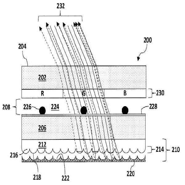
도 4는 본원에서 설명하는 반사 구조체를 도시하는데, 여기서 반구형 어레이 밑에 배치된 반사 요소는 대략 구형 요홈들의 어레이를 포함하고, 또한 어두운 동공 지역들을 통과하는 광선들이 어떻게 준재귀반사(semi-retro-reflection)하는지를 도시한다. 도 4는 관측자를 향한 외부면(102)과 관측자에 대향하는 내부면(104)을 가진 투명 시트(100)를 도시한다. 시트(100)는 개별 반구체들(108) 안에서 내부 전반사(total internal reflection (TIR))에 의해 빛을 반사하는 복수 개의 볼록 돌출부, 반구 돌출부, 또는 반구체(106)를 더 포함한다. 반구체들(108)은 반구 비드들 또는 반 비드들일 수도 있다. 도 4의 반사 구조체는 시트(100)와 인접면(104) 뒤에 놓인 반사면(122)을 가진 반사 요소(120)를 더 포함한다. 반사 요소(120)는 복수 개의 구형 요홈(124)을 포함하는데, 그 각각은 그 바로 위에 위치한 반구체의 곡률 중심과 실질적으로 일치하는 곡률 반경을 가진다. 두 곡률 반경의 비는 재귀반사와 관련된 각편차도에 영향을 미친다 (여기서는 (구형 요홈의 곡률 반경)/(반구체의 곡률 반경)). 시트(100)를 통과하는 입사 광선들(110)(실선들로 도시)은 절반 정도가 반구 돌출부들(108)의 면(104)에서 일반적으로 내부에서 전반사되고 대부분 재귀반사되지만 빠져 나온 광선(112)(점선으로 도시)에 도시된 바와 같이 반드시 광원을 향해 바로 돌아가는 것은 아니다. 내부에서 전반사되지 않은 나머지 광선들(114)은 개별 반구 돌출부들(108)의 어두운 동공을 통과해, 복수 개의 구형 요홈(124)을 포함하는 반사 요소의 윤곽면(122)에서 준재귀반사한다. 입사 광선의 방향이 평면 반사 요소의 표면에 직교 방향이 아닐 때 광선들(118)이 광원에서 멀어지게 반사되는 도 3에 설명된 평면 반사 요소와 달리, 광선들(114)은 실질적으로 반구체를 향해 돌아가고, 이에 준재귀반사 방식으로 광원을 향하는 광선들(112)처럼 빠져나간다. 이 광선들은 내부 전반사 광선들과 결합해 반사도를 증진한다. Figure 4 shows a reflective structure as described herein wherein a reflective element disposed under the hemispherical array comprises an array of substantially spherical grooves and also shows how the rays passing through the dark pupil regions are reflected by a semi- ). Figure 4 shows a
도 4에 설명된 구조체는 반사 디스플레이의 반사율과 겉보기 밝기를 증진하기 위해 반사 디스플레이에 결합될 수 있다. 도 5의 실시예는 도 4에 도시된 반사 구조체의 반사 디스플레이에 대한 결합을 도시한다. 도 5의 디스플레이(200)는 투명 전방 시트(202)를 포함하는데, 투명 전방 시트는 예를 들어 유리 또는 고분자로 구성되고 관찰자를 향한 외면(204)을 가진다. 디스플레이(200)는 제2 투명 시트(206)를 더 포함하는데, 제2 투명 시트는 예를 들어 유리 또는 고분자로 구성되고, 광변조 층을 포함하는 캐비티(208)를 형성한다. 캐비티(208)에 대해 시트(206)의 반대편에는 도 4에 설명된 것과 유사한 후방 반사 구조체(210)가 있다. 반사 구조체(210)는 개별 반구체들(216) 안에서 내부 전반사(TIR)에 의해 빛을 반사하는 복수 개의 볼록 돌출부 또는 반구 돌출부(즉, 반구체)(214)를 더 포함하는 투명 시트(212)를 포함한다. 복수 개의 반구체(214)는 반사면(222)을 가지는 복수 개의 구형 요홈을 포함하는 반사 요소(220)가 인접하는 윤곽면(218)을 형성한다. 일 실시예에서, 두 곡률 반경의 비는 약 0.5 내지 5이다(여기서 (구형 요홈의 곡률 반경)/(반구체의 곡률 반경))은 약 0.5 내지 5). 또 다른 실시예에서, 두 곡률 반경의 비는 약 1 내지 3이다. 또 다른 실시예에서, 두 곡률 반경의 비는 약 1 내지 2이다. 도시되지 않았지만, 도 5의 디스플레이(200)은 광학 전방 조명을 더 포함할 수 있다.The structure described in FIG. 4 may be coupled to a reflective display to enhance the reflectivity and apparent brightness of the reflective display. The embodiment of FIG. 5 illustrates the coupling of the reflective structure shown in FIG. 4 to a reflective display. The
도 5의 디스플레이(200)의 광변조 층(208)은 입사광이 후방 반사 요소(214)를 향해 시트(206)를 통과하는 것을 허용하거나 막는다. 광변조 층은, 반사광의 편광에 의존하지 않는 미세 전자 기계 시스템(micro-electromechanical system (MEMS)), 전기습윤 시스템, 전기영동 이동 입자들 또는 그 조합과 같은, 하지만 이에 한정되지는 않는 임의 개수의 기술들에 기초한 광학 셔터를 포함할 수도 있다. 디스플레이(200)는 부유 전기영동 이동 입자들(226)을 가진 액체 매개체(224)를 포함하는 광변조 층을 도시한다. 캐비티(208) 내부, 투명 시트(206)의 앞면 상에 전극층(228)이 있는데, 전극층은 박막 트랜지스터 어레이, 패턴 전극 어레이, 또는 그 조합을 포함할 수도 있다. 전압원(미도시)과 조합된 전극층(228)은 광변조 층을 제어한다. 전극층이 액체 매개체(224)에 인접하는 컬러 필터층의 뒷면에 위치하는 것도 생각할 수 있다. 디스플레이(200)는 도 5에서 R, G, 및 B로 각각 표시된 적색, 녹색, 및 청색 서브 픽셀들을 더 포함하는 광학 컬러 필터 어레이 층(230)을 더 포함한다. 대안적으로, 서브 픽셀들은 시안색, 마젠타색, 및 황색으로 구성될 수도 있다.The light modulating
도 5의 디스플레이(200)에 도시된 바와 같이, 광변조 층은 빛을 통과시키도록 설정된다. 입사 및 반사 광선들(232)이 통과하도록 전기영동 이동 입자들(226)이 전극층(228)의 특정한 위치들에 국지적으로 배치되거나 모이도록, 적절한 극성 전압이 인가된다. 입사 광선들이 실선들로 도시되고 반사 광선들이 점선들로 도시된다. 디스플레이(200)의 몇 개의 층을 통과하는 광선들은 볼록 돌출부나 반구형 어레이(214)에서 내부적으로 전반사되거나 개별 반구체들(216)의 어두운 동공 영역들을 통과한다. 어두운 동공들을 통과하는 광선들은 실질적으로 왔던(즉, 출발점) 방향으로부터 관측자를 향해 반사되도록 반사 요소(220)의 면(222)에서 재귀반사되어, 디스플레이의 겉보기 밝기를 증진한다.As shown in
도 5는 본원에서 설명하는 전체 설계의 중요한 특성을 도시한다. 이는 높은 효율(즉, 입사 광선들의 높은 반사도)을 얻는 것뿐만 아니라, 재귀반사 특성이 녹색 서브 픽셀 필터를 통과하도록 도시된 입사광이 실질적으로 컬러 필터층(230)의 동일한 녹색 서브 픽셀 필터를 통해 입사광의 방향으로 다시 돌아가도록 한다. 이는 반사 컬러 디스플레이에서 높은 효율과 높은 색포화도를 얻는 데 중요하다. 반사 구조체(210)는 밝은 흰색 종이 같은 외관의 생산을 용이하게 하면서 컬러 필터들이 포화색을 내게 하는 것을 효율적으로 가능하게 한다. 이런 특성들은 넓은 범위의 입사 시야각들에 걸쳐 유지되면서 우수한 인체 공학적 시야 특성을 제공한다.FIG. 5 illustrates an important characteristic of the overall design described herein. This is because not only is it possible to obtain high efficiency (i.e. high reflectivity of incident light rays), but also that the incident light, which is shown so that the retroreflective characteristic passes through the green subpixel filter, is substantially absorbed through the same green subpixel filter of the
도 6의 디스플레이(200)에 도시된 바와 같이, 부유 전기영동 이동 입자들(226)을 함유하는 액체 매개체(224)를 포함하는 광변조 층이 빛 투과를 막도록 설정된다. 이 예에서, 입자들은 적절한 극성의 전기장 인가에 의해 국지적인 배치에서 벗어나 전극층(228) 상에서 실질적으로 균일한 층을 이루어, 외부 투명 시트(202)와 광학 컬러 필터층(230)을 통과하는 입사 광선들(232)이 입자들의 층(226)에 흡수되도록 하면서, 빛이 반사되는 것을 막아 디스플레이의 어두운 상태를 만들도록 한다. 대안적으로, 전극층(228)이 디스플레이(200) 안의 컬러 필터층(230) 내면에 위치하는 것을 생각할 수 있다.As shown in
본원에서 설명한 디스플레이 실시예들은 전자책 판독기, 휴대용 컴퓨터, 태블릿 컴퓨터, 착용 장치, 휴대폰, 스마트 카드, 간판, 시계, 선반 라벨, 플래시 드라이브, 및 옥외 게시판 또는 옥외 간판과 같은 곳에, 하지만 이에 한정되지 않게 적용될 수 있다.The display embodiments described herein may be used in various applications such as, but not limited to, electronic book readers, portable computers, tablet computers, worn devices, cell phones, smart cards, signage, clocks, shelf labels, flash drives, Can be applied.
위에서 설명한 실시예들은 이러한 적용을 도시하지만 이를 한정하지는 않는다. 다양한 예시적 측면들 및 실시예들이 위에서 논의되었지만, 당업자들은 소정의 여러 변경, 치환, 추가, 및 그 준조합을 인지할 것이다. 그러므로, 본 개시의 범위는 다음의 청구범위에 의해서만 정의된다.The embodiments described above illustrate this application, but do not limit it. While various illustrative aspects and embodiments have been discussed above, those skilled in the art will recognize various changes, substitutions, additions, and subcombinations thereof. Therefore, the scope of the present disclosure is defined only by the following claims.
Claims (21)
제1 광학적 투명 시트;
적어도 하나의 전극층;
복수 개의 볼록 또는 반구 돌출부를 더 포함하는 면을 가지는 제2 광학적 투명 시트;
상기 볼록 또는 반구 돌출부들의 어두운 공동 영역들을 통과하는 빛을 실질적으로 준재귀반사(semi-retro-reflection)하는 반사 증진층;
빛이 차단되거나 통과되는 적어도 하나의 광변조 층; 및
상기 광변조 층을 제어 가능하게 조절하기 위한 전압원을 포함하는 반사 디스플레이.In a reflective display having a brightness enhancement structure,
A first optical transparent sheet;
At least one electrode layer;
A second optical transparent sheet having a surface further comprising a plurality of convex or hemispherical protrusions;
A reflective enhancement layer that substantially semi-retro-reflections the light passing through the dark cavities of the convex or hemispherical protrusions;
At least one light modulating layer through which light is blocked or passed; And
And a voltage source for controllably adjusting the light modulation layer.
상기 광변조 층에 제2 극성의 전압을 인가해 빛을 차단하도록 전환 가능한
반사 디스플레이.[2] The apparatus of claim 1, wherein the voltage source is switchable to apply light of one polarity to the optical modulation layer to pass light therethrough; And
And a second polarity voltage is applied to the optical modulation layer
Reflective display.
제2 극성 전압의 인가에 의한 상기 전기영동 이동 입자들의 이동은 비조명 상태를 만드는 반사 디스플레이.8. The method of claim 7, wherein movement of the electrophoretic moving particles by application of a unipolar voltage creates an illumination condition,
Wherein movement of said electrophoretic moving particles by application of a second polar voltage creates a non-illuminated state.
Applications Claiming Priority (3)
| Application Number | Priority Date | Filing Date | Title |
|---|---|---|---|
| US201361826236P | 2013-05-22 | 2013-05-22 | |
| US61/826,236 | 2013-05-22 | ||
| PCT/US2014/038091 WO2014189751A1 (en) | 2013-05-22 | 2014-05-15 | Method and apparatus for improved color filter saturation |
Publications (1)
| Publication Number | Publication Date |
|---|---|
| KR20160013908A true KR20160013908A (en) | 2016-02-05 |
Family
ID=51933984
Family Applications (1)
| Application Number | Title | Priority Date | Filing Date |
|---|---|---|---|
| KR1020157035285A Ceased KR20160013908A (en) | 2013-05-22 | 2014-05-15 | Method and apparatus for improved color filter saturation |
Country Status (6)
| Country | Link |
|---|---|
| US (1) | US10203436B2 (en) |
| EP (1) | EP2999989A4 (en) |
| JP (1) | JP6469656B2 (en) |
| KR (1) | KR20160013908A (en) |
| CN (1) | CN105264422B (en) |
| WO (1) | WO2014189751A1 (en) |
Families Citing this family (15)
| Publication number | Priority date | Publication date | Assignee | Title |
|---|---|---|---|---|
| KR20160013908A (en) | 2013-05-22 | 2016-02-05 | 클리어잉크 디스플레이스 엘엘씨 | Method and apparatus for improved color filter saturation |
| US10705404B2 (en) | 2013-07-08 | 2020-07-07 | Concord (Hk) International Education Limited | TIR-modulated wide viewing angle display |
| EP3204800A4 (en) | 2014-10-08 | 2018-06-06 | Clearink Displays, Inc. | Color filter registered reflective display |
| US10386691B2 (en) | 2015-06-24 | 2019-08-20 | CLEARink Display, Inc. | Method and apparatus for a dry particle totally internally reflective image display |
| US10386547B2 (en) | 2015-12-06 | 2019-08-20 | Clearink Displays, Inc. | Textured high refractive index surface for reflective image displays |
| US10261221B2 (en) | 2015-12-06 | 2019-04-16 | Clearink Displays, Inc. | Corner reflector reflective image display |
| US20200341176A1 (en) * | 2017-05-03 | 2020-10-29 | Clearink Displays, Inc. | Static semi-retro-reflective displays |
| EP3704541A4 (en) * | 2017-11-03 | 2021-08-18 | Concord (Hk) International Education Limited | Method, system and apparatus for reflective-emissive hybrid display |
| CN108445690B (en) | 2018-03-19 | 2020-07-31 | 京东方科技集团股份有限公司 | Display modules and electronic equipment |
| EP3776056B1 (en) * | 2018-04-10 | 2024-05-29 | Concord (HK) International Education Limited | Convex protrusions in total internal reflection based image displays |
| US11614653B2 (en) * | 2018-07-03 | 2023-03-28 | Concord (Hk) International Education Limited | Color filter arrays for TIR-based image displays |
| TWI696307B (en) * | 2018-10-19 | 2020-06-11 | 致伸科技股份有限公司 | Display device |
| CN113156732B (en) * | 2021-05-31 | 2024-09-10 | 京东方科技集团股份有限公司 | Reflective display panel and manufacturing method thereof, and display device |
| TWI786775B (en) * | 2021-08-19 | 2022-12-11 | 友達光電股份有限公司 | Display apparatus |
| EP4544351A1 (en) * | 2022-06-24 | 2025-04-30 | Corning Incorporated | Reflective displays including reflectors |
Family Cites Families (200)
| Publication number | Priority date | Publication date | Assignee | Title |
|---|---|---|---|---|
| US3792308A (en) | 1970-06-08 | 1974-02-12 | Matsushita Electric Industrial Co Ltd | Electrophoretic display device of the luminescent type |
| US3919031A (en) * | 1974-04-12 | 1975-11-11 | Rohm & Haas | Retroreflective film |
| JPS51144198A (en) * | 1975-06-06 | 1976-12-10 | Seibu Polymer Kasei Kk | Return reflector |
| US4071430A (en) | 1976-12-06 | 1978-01-31 | North American Philips Corporation | Electrophoretic image display having an improved switching time |
| US4203106A (en) | 1977-11-23 | 1980-05-13 | North American Philips Corporation | X-Y addressable electrophoretic display device with control electrode |
| US4648956A (en) | 1984-12-31 | 1987-03-10 | North American Philips Corporation | Electrode configurations for an electrophoretic display device |
| JPH0691252B2 (en) | 1986-11-27 | 1994-11-14 | 日本電気株式会社 | Thin film transistor array |
| US5019748A (en) | 1986-12-12 | 1991-05-28 | E-Lite Technologies, Inc. | Method for making an electroluminescent panel lamp as well as panel lamp produced thereby |
| US5319491A (en) | 1990-08-10 | 1994-06-07 | Continental Typographics, Inc. | Optical display |
| EP0632919B1 (en) | 1992-02-25 | 1999-04-28 | Copytele Inc. | Electrophoretic display panel for blinking displayed characters |
| US5396350A (en) | 1993-11-05 | 1995-03-07 | Alliedsignal Inc. | Backlighting apparatus employing an array of microprisms |
| US6025897A (en) | 1993-12-21 | 2000-02-15 | 3M Innovative Properties Co. | Display with reflective polarizer and randomizing cavity |
| US5596671A (en) | 1994-04-28 | 1997-01-21 | Rockwell, Iii; Marshall A. | Optical waveguide display system |
| US7848006B2 (en) | 1995-07-20 | 2010-12-07 | E Ink Corporation | Electrophoretic displays with controlled amounts of pigment |
| US7259744B2 (en) * | 1995-07-20 | 2007-08-21 | E Ink Corporation | Dielectrophoretic displays |
| US7215451B1 (en) | 1996-04-15 | 2007-05-08 | Dai Nippon Printing Co., Ltd. | Reflection type diffuse hologram, hologram for reflection hologram color filters, etc., and reflection type display device using such holograms |
| US5871653A (en) | 1996-10-30 | 1999-02-16 | Advanced Materials Engineering Research, Inc. | Methods of manufacturing micro-lens array substrates for implementation in flat panel display |
| US5959777A (en) | 1997-06-10 | 1999-09-28 | The University Of British Columbia | Passive high efficiency variable reflectivity image display device |
| US6215920B1 (en) | 1997-06-10 | 2001-04-10 | The University Of British Columbia | Electrophoretic, high index and phase transition control of total internal reflection in high efficiency variable reflectivity image displays |
| US6064784A (en) | 1997-06-10 | 2000-05-16 | The University Of British Columbia | Electrophoretic, dual refraction frustration of total internal reflection in high efficiency variable reflectivity image displays |
| US8040594B2 (en) | 1997-08-28 | 2011-10-18 | E Ink Corporation | Multi-color electrophoretic displays |
| US6067185A (en) | 1997-08-28 | 2000-05-23 | E Ink Corporation | Process for creating an encapsulated electrophoretic display |
| US6377383B1 (en) | 1997-09-04 | 2002-04-23 | The University Of British Columbia | Optical switching by controllable frustration of total internal reflection |
| US5999307A (en) | 1997-09-04 | 1999-12-07 | The University Of British Columbia | Method and apparatus for controllable frustration of total internal reflection |
| US7075502B1 (en) | 1998-04-10 | 2006-07-11 | E Ink Corporation | Full color reflective display with multichromatic sub-pixels |
| WO2000020923A1 (en) | 1998-10-07 | 2000-04-13 | E Ink Corporation | Illumination system for nonemissive electronic displays |
| US6850312B2 (en) | 1999-03-16 | 2005-02-01 | Alien Technology Corporation | Apparatuses and methods for flexible displays |
| US6930818B1 (en) | 2000-03-03 | 2005-08-16 | Sipix Imaging, Inc. | Electrophoretic display and novel process for its manufacture |
| JP2001310334A (en) * | 2000-04-27 | 2001-11-06 | Hitachi Chem Co Ltd | Transfer original mold, rugged mold, manufacturing method thereof, transferring laminate and diffuse reflecting plate |
| US6304365B1 (en) | 2000-06-02 | 2001-10-16 | The University Of British Columbia | Enhanced effective refractive index total internal reflection image display |
| JP4053260B2 (en) | 2000-10-18 | 2008-02-27 | シャープ株式会社 | Organic electroluminescence display element |
| EP1330844A1 (en) | 2000-11-02 | 2003-07-30 | 3M Innovative Properties Company | Brightness and contrast enhancement of direct view emissive displays |
| US6384979B1 (en) | 2000-11-30 | 2002-05-07 | The University Of British Columbia | Color filtering and absorbing total internal reflection image display |
| TW574512B (en) | 2001-03-14 | 2004-02-01 | Koninkl Philips Electronics Nv | Electrophoretic display device |
| WO2002079869A1 (en) | 2001-04-02 | 2002-10-10 | E Ink Corporation | Electrophoretic medium with improved image stability |
| US8390918B2 (en) | 2001-04-02 | 2013-03-05 | E Ink Corporation | Electrophoretic displays with controlled amounts of pigment |
| WO2002093245A1 (en) | 2001-05-15 | 2002-11-21 | E Ink Corporation | Electrophoretic displays containing magnetic particles |
| US20100148385A1 (en) | 2001-05-15 | 2010-06-17 | E Ink Corporation | Electrophoretic media and processes for the production thereof |
| US6822783B2 (en) | 2001-06-26 | 2004-11-23 | Canon Kabushiki Kaisha | Electrophoretic display unit, and driving method thereof |
| JP2003091002A (en) * | 2001-07-12 | 2003-03-28 | Alps Electric Co Ltd | Liquid crystal display device |
| JP2003043232A (en) * | 2001-07-31 | 2003-02-13 | Seiko Epson Corp | Reflection plate and manufacturing method thereof, liquid crystal display device, electronic device |
| US6437921B1 (en) | 2001-08-14 | 2002-08-20 | The University Of British Columbia | Total internal reflection prismatically interleaved reflective film display screen |
| US6819471B2 (en) | 2001-08-16 | 2004-11-16 | E Ink Corporation | Light modulation by frustration of total internal reflection |
| JP4211312B2 (en) | 2001-08-20 | 2009-01-21 | セイコーエプソン株式会社 | Electrophoresis device, electrophoretic device driving method, electrophoretic device driving circuit, and electronic apparatus |
| US7852430B1 (en) | 2001-11-29 | 2010-12-14 | Palm, Inc. | Light guide spacers for backlighting a reflective display |
| US6452734B1 (en) | 2001-11-30 | 2002-09-17 | The University Of British Columbia | Composite electrophoretically-switchable retro-reflective image display |
| US7126214B2 (en) | 2001-12-05 | 2006-10-24 | Arbor Company Llp | Reconfigurable processor module comprising hybrid stacked integrated circuit die elements |
| WO2003050607A1 (en) | 2001-12-13 | 2003-06-19 | E Ink Corporation | Electrophoretic electronic displays with films having a low index of refraction |
| SG102064A1 (en) | 2001-12-25 | 2004-02-27 | Toray Industries | Color filter, liquid crystal display device, and method for making color filter |
| ES2385017T3 (en) | 2002-02-19 | 2012-07-17 | Samsung Lcd Netherlands R&D Center B.V. | Display device |
| AU2003219894A1 (en) | 2002-02-26 | 2003-09-09 | Uni-Pixel Displays, Inc. | Enhancements to optical flat panel displays |
| US6891658B2 (en) | 2002-03-04 | 2005-05-10 | The University Of British Columbia | Wide viewing angle reflective display |
| US7804236B2 (en) | 2002-03-20 | 2010-09-28 | Copytele, Inc. | Flat panel display incorporating control frame |
| JP4410456B2 (en) | 2002-04-24 | 2010-02-03 | 株式会社リコー | Thin film device device manufacturing method and active matrix substrate manufacturing method |
| US7554712B2 (en) | 2005-06-23 | 2009-06-30 | E Ink Corporation | Edge seals for, and processes for assembly of, electro-optic displays |
| US6842279B2 (en) | 2002-06-27 | 2005-01-11 | E Ink Corporation | Illumination system for nonemissive electronic displays |
| US6865011B2 (en) | 2002-07-30 | 2005-03-08 | The University Of British Columbia | Self-stabilized electrophoretically frustrated total internal reflection display |
| JP2004085635A (en) | 2002-08-22 | 2004-03-18 | Tdk Corp | Display device |
| CN100397227C (en) | 2002-09-03 | 2008-06-25 | 伊英克公司 | Electrophoretic medium and method of forming electrophoretic medium |
| EP1599759A1 (en) | 2003-02-20 | 2005-11-30 | Koninklijke Philips Electronics N.V. | Electrophoretic multi-color display device |
| JP2004271610A (en) | 2003-03-05 | 2004-09-30 | Canon Inc | Color electrophoretic display |
| US7046439B2 (en) | 2003-05-22 | 2006-05-16 | Eastman Kodak Company | Optical element with nanoparticles |
| TWI220749B (en) | 2003-08-12 | 2004-09-01 | Toppoly Optoelectronics Corp | Altering resolution circuit apparatus of liquid crystal display panel |
| GB0328005D0 (en) | 2003-12-03 | 2004-01-07 | Koninkl Philips Electronics Nv | 2D/3D Displays |
| US7079304B2 (en) | 2004-01-23 | 2006-07-18 | The Lubrizol Corporation | Structured fluid compositions for electrophoretically frustrated total internal reflection displays |
| EP1743197B1 (en) | 2004-04-23 | 2011-08-10 | Olivier M. Parriaux | High efficiency optical diffraction device |
| US7286280B2 (en) | 2004-05-07 | 2007-10-23 | The University Of British Columbia | Brightness enhancement film for backlit image displays |
| US7564614B2 (en) | 2004-05-20 | 2009-07-21 | Sipix Imaging, Inc. | Electrode protection film for electrophoretic displays |
| WO2005124404A1 (en) | 2004-06-17 | 2005-12-29 | Koninklijke Philips Electronics N.V. | An optical separating filter |
| US7093968B2 (en) | 2004-08-19 | 2006-08-22 | Radiant Opto-Electronics Corporation | Light guide plate and LGP-based FFP |
| US7775700B2 (en) | 2004-10-01 | 2010-08-17 | Rohm And Haas Electronics Materials Llc | Turning film using array of roof prism structures |
| KR20070074566A (en) | 2004-10-20 | 2007-07-12 | 유니버시티 오브 플로리다 리서치 파운데이션, 인크. | Dual light emitting and electrochromic device |
| TWI249191B (en) * | 2004-12-31 | 2006-02-11 | Au Optronics Corp | Method for fabricating a microelectromechanical optical display device |
| US7164536B2 (en) | 2005-03-16 | 2007-01-16 | The University Of British Columbia | Optically coupled toroidal lens:hemi-bead brightness enhancer for total internal reflection modulated image displays |
| CN100520552C (en) | 2005-04-15 | 2009-07-29 | 不列颠哥伦比亚大学 | Brightness enhancement in tir-modulated electrophoretic reflective image displays |
| JP2008535005A (en) | 2005-04-15 | 2008-08-28 | ザ ユニバーシティ オブ ブリティッシュ コロンビア | Brightness improvement of TIR modulation electrophoretic reflection image display |
| WO2006114743A2 (en) | 2005-04-27 | 2006-11-02 | Koninklijke Philips Electronics N.V. | Backlighting system and display system |
| KR100638874B1 (en) | 2005-07-06 | 2006-10-27 | 삼성전기주식회사 | A light source-light guide plate structure of a backlight device having an LED light source inserted into the light guide plate and a backlight device including the same |
| US20070019434A1 (en) | 2005-07-22 | 2007-01-25 | Eastman Kodak Company | Turning film having variable pitch |
| JP4894201B2 (en) | 2005-08-26 | 2012-03-14 | 富士ゼロックス株式会社 | Image display device and image display method |
| US7751115B2 (en) | 2005-08-26 | 2010-07-06 | Lg Electronics Inc. | Electronic paper display device, manufacturing method and driving method thereof |
| US20090231714A1 (en) | 2005-09-19 | 2009-09-17 | Yang Zhao | Transparent anti-reflective article and method of fabricating same |
| JP4682767B2 (en) | 2005-09-21 | 2011-05-11 | ブラザー工業株式会社 | Forming method for forming partition and spacer of electrophoretic display medium on substrate, and electrophoretic display medium formed by forming method of partition and spacer forming partition and spacer of electrophoretic display medium on substrate |
| US20070091434A1 (en) | 2005-10-21 | 2007-04-26 | Hewlett-Packard Development Company, L.P. | Luminance adjustment |
| JP5020961B2 (en) | 2005-10-27 | 2012-09-05 | コーニンクレッカ フィリップス エレクトロニクス エヌ ヴィ | Directional light output device such as multi-view display |
| KR101302089B1 (en) * | 2005-12-19 | 2013-08-30 | 픽스트로닉스 인코포레이티드 | Direct-View MEMS Display Devices and Methods for Generating Images Thereon |
| JP2009520234A (en) | 2005-12-20 | 2009-05-21 | コーニンクレッカ フィリップス エレクトロニクス エヌ ヴィ | Improved in-plane switching electrophoretic display |
| US20100085627A1 (en) * | 2006-01-17 | 2010-04-08 | The University Of British Columbia | Microlens-assisted brightness enhancement in reflective image displays |
| TW200732733A (en) | 2006-02-17 | 2007-09-01 | Ind Tech Res Inst | Hybrid display |
| JP2007219346A (en) | 2006-02-20 | 2007-08-30 | Seiko Epson Corp | Liquid crystal device and electronic device |
| CN101405644B (en) | 2006-03-20 | 2010-12-01 | 夏普株式会社 | display device |
| JP2007279641A (en) * | 2006-04-12 | 2007-10-25 | Funai Electric Advanced Applied Technology Research Institute Inc | Reflective display device |
| WO2007118306A1 (en) | 2006-04-19 | 2007-10-25 | The University Of British Columbia | Ionic electrophoresis in tir-modulated reflective image displays |
| US20070263137A1 (en) | 2006-05-09 | 2007-11-15 | Victor Company Of Japan, Limited | Illuminating device and display device |
| US20070263291A1 (en) | 2006-05-15 | 2007-11-15 | The University Of British Columbia | Micro-hemisphere array fabrication |
| US7660509B2 (en) | 2006-05-24 | 2010-02-09 | 3M Innovative Properties Company | Backlight asymmetric light input wedge |
| US7740387B2 (en) | 2006-05-24 | 2010-06-22 | 3M Innovative Properties Company | Backlight wedge with side mounted light source |
| JP4185120B2 (en) | 2006-06-30 | 2008-11-26 | 株式会社東芝 | Display device |
| US7808696B2 (en) | 2006-07-31 | 2010-10-05 | Samsung Electronics Co., Ltd. | Electrophoretic display device and fabrication thereof |
| TWI340846B (en) | 2006-08-04 | 2011-04-21 | Au Optronics Corp | Pixel structure of a transflective liquid crystal panel having a single gap |
| TWI344050B (en) | 2006-08-18 | 2011-06-21 | Au Optronics Corp | Transflective liquid crystal display panel |
| US7656577B2 (en) | 2006-11-20 | 2010-02-02 | Samsung Electronics Co., Ltd. | Color filter substrate, electrophoretic display device having the same, and method of manufacturing the same |
| JP4345820B2 (en) | 2007-01-22 | 2009-10-14 | セイコーエプソン株式会社 | Display device, display device manufacturing method, and electronic paper |
| GB0702347D0 (en) * | 2007-02-07 | 2007-03-21 | Plastic Logic Ltd | Electronic document reading devices |
| US7576905B2 (en) | 2007-02-23 | 2009-08-18 | 3M Innovative Properties Company | Electrostatically-controlled diffraction gratings using ionic electrophoresis |
| JP2008288195A (en) | 2007-03-07 | 2008-11-27 | Rohm & Haas Denmark Finance As | Backlight unit with reduced color separation containing polarization conversion film |
| WO2008122927A1 (en) | 2007-04-06 | 2008-10-16 | Koninklijke Philips Electronics N.V. | Reflective display and method for manufacturing such a display |
| US7507012B2 (en) | 2007-05-16 | 2009-03-24 | Rohm And Haas Denmark Finance A/S | LCD displays with light redirection |
| JP4549363B2 (en) | 2007-05-18 | 2010-09-22 | 株式会社リコー | Electrophoretic particles and image display device using the same |
| US8179034B2 (en) | 2007-07-13 | 2012-05-15 | 3M Innovative Properties Company | Light extraction film for organic light emitting diode display and lighting devices |
| US8022615B2 (en) | 2007-08-14 | 2011-09-20 | Motorola Mobility, Inc. | Light generating layer for a reflective display |
| US9224342B2 (en) | 2007-10-12 | 2015-12-29 | E Ink California, Llc | Approach to adjust driving waveforms for a display device |
| KR101388582B1 (en) | 2007-10-26 | 2014-04-23 | 삼성디스플레이 주식회사 | Electrophoretic display device |
| KR100972097B1 (en) | 2007-11-26 | 2010-07-22 | 삼성코닝정밀소재 주식회사 | Multifunctional Optical Film for Display Device Using Electrophoresis |
| JP2011511965A (en) | 2008-02-08 | 2011-04-14 | レイセオン カンパニー | Electrophoretic light modulator |
| WO2009102731A2 (en) | 2008-02-12 | 2009-08-20 | Qualcomm Mems Technologies, Inc. | Devices and methods for enhancing brightness of displays using angle conversion layers |
| BRPI0820651A2 (en) | 2008-03-03 | 2019-09-24 | Sharp Kk | liquid crystal display device |
| US7630222B2 (en) | 2008-03-25 | 2009-12-08 | Delta Electronics, Inc. | Inverter apparatus with adaptable voltage-to-frequency control |
| JP2009251215A (en) | 2008-04-04 | 2009-10-29 | Dainippon Printing Co Ltd | Electrophoretic display device |
| US20090256810A1 (en) | 2008-04-15 | 2009-10-15 | Sony Ericsson Mobile Communications Ab | Touch screen display |
| US20090262083A1 (en) | 2008-04-16 | 2009-10-22 | Jateen Parekh | Systems and methods for receiving user input through a display with a flexible backplane via touch sensors |
| US8570636B2 (en) | 2008-04-18 | 2013-10-29 | Zikon Inc. | Systems, methods and compositions relating to display elements |
| JP4577429B2 (en) | 2008-04-30 | 2010-11-10 | ソニー株式会社 | Liquid crystal display |
| US7940457B2 (en) | 2008-05-30 | 2011-05-10 | The Board Of Trustees Of The University Of Illinois | Energy-efficient optoelectronic smart window |
| KR20110047242A (en) | 2008-08-22 | 2011-05-06 | 유니-픽셀 디스플레이스, 인코포레이티드 | A normally emitting pixel architecture for frustrated total internal reflection displays |
| US8264637B2 (en) | 2008-10-10 | 2012-09-11 | Samsung Electronics Co., Ltd. | Photonic crystal optical filter, reflective color filter, display apparatus using the reflective color filter, and method of manufacturing the reflective color filter |
| KR101103408B1 (en) * | 2008-12-29 | 2012-01-05 | 제일모직주식회사 | Electrophoretic display with improved reflectance |
| TW201024886A (en) | 2008-12-29 | 2010-07-01 | Ind Tech Res Inst | Display structure |
| US20110085116A1 (en) | 2009-01-13 | 2011-04-14 | Kim Eun-Seok | Dual layer holographic color filter and transmissive liquid crystal display using the same |
| US8905610B2 (en) | 2009-01-26 | 2014-12-09 | Flex Lighting Ii, Llc | Light emitting device comprising a lightguide film |
| JP5316100B2 (en) | 2009-03-06 | 2013-10-16 | 富士ゼロックス株式会社 | Display particle dispersion, display medium, and display device |
| US9217906B2 (en) | 2009-03-26 | 2015-12-22 | Hewlett-Packard Development Company, L.P. | In-plane electro-optical display |
| US8237733B2 (en) | 2009-03-31 | 2012-08-07 | Ricoh Co., Ltd. | Page transition on electronic paper display |
| CN102804039A (en) * | 2009-06-30 | 2012-11-28 | 惠普开发有限公司 | Full-color reflective display |
| KR101256545B1 (en) | 2009-08-05 | 2013-04-19 | 엘지디스플레이 주식회사 | In-plane switching mode transflective type liquid crystal display device |
| US8648772B2 (en) | 2009-08-20 | 2014-02-11 | Amazon Technologies, Inc. | Amalgamated display comprising dissimilar display devices |
| US8144270B2 (en) | 2009-09-02 | 2012-03-27 | United Microelectronics Corp. | Color filter device and method for fabricating the same |
| JP2011095708A (en) * | 2009-10-02 | 2011-05-12 | Toppan Printing Co Ltd | Image display device, transparent structure with fine mirror, and manufacturing methods thereof |
| WO2011044439A1 (en) | 2009-10-08 | 2011-04-14 | The Penn State Research Foundation | Multi-spectral filters, mirrors and antireflective coatings with subwavelength periodic features for optical devices |
| WO2011058725A1 (en) | 2009-11-10 | 2011-05-19 | パナソニック株式会社 | Display device and method of manufacture thereof |
| JP5381671B2 (en) | 2009-12-11 | 2014-01-08 | 富士ゼロックス株式会社 | Display device |
| JP5077367B2 (en) | 2010-01-28 | 2012-11-21 | 凸版印刷株式会社 | Color filter substrate for transflective liquid crystal display device, manufacturing method thereof, and transflective liquid crystal display device |
| US9028123B2 (en) | 2010-04-16 | 2015-05-12 | Flex Lighting Ii, Llc | Display illumination device with a film-based lightguide having stacked incident surfaces |
| US8860658B2 (en) | 2010-05-17 | 2014-10-14 | Creator Technology B.V. | Electrophoretic display unit and method for driving an electrophoretic display panel |
| KR20110134161A (en) * | 2010-06-08 | 2011-12-14 | 삼성전자주식회사 | Reflective color display device |
| US8184357B2 (en) | 2010-06-15 | 2012-05-22 | Hewlett-Packard Development Company, L.P. | Display element |
| US8384659B2 (en) | 2010-06-15 | 2013-02-26 | Hewlett-Packard Development Company, L.P. | Display element including electrodes and a fluid with colorant particles |
| JP5741829B2 (en) | 2010-06-18 | 2015-07-01 | ソニー株式会社 | Electrophoretic element, display device and electronic device |
| US8723759B2 (en) | 2010-06-23 | 2014-05-13 | Sharp Kabushiki Kaisha | Display with light concentrating substrate |
| JP2012027163A (en) | 2010-07-22 | 2012-02-09 | Casio Comput Co Ltd | Electrophoretic display device |
| KR20140015248A (en) | 2010-08-09 | 2014-02-06 | 휴렛-팩커드 디벨롭먼트 컴퍼니, 엘.피. | System and method for tri-state electro-optical displays |
| JP5531877B2 (en) | 2010-09-14 | 2014-06-25 | セイコーエプソン株式会社 | Electro-optic display device and manufacturing method thereof |
| US8693081B2 (en) | 2010-09-30 | 2014-04-08 | University Of Cincinnati | Electrofluidic imaging film, devices, and displays, and methods of making and using the same |
| JP5594069B2 (en) | 2010-11-05 | 2014-09-24 | セイコーエプソン株式会社 | Electrophoretic display device and electronic apparatus |
| US8690408B2 (en) | 2010-12-03 | 2014-04-08 | At&T Intellectual Property I, L. P. | Methods, systems, and products for illuminating displays |
| EP2684080A2 (en) | 2011-03-08 | 2014-01-15 | Dolby Laboratories Licensing Corporation | Illuminator for reflective displays |
| US20120262496A1 (en) * | 2011-04-18 | 2012-10-18 | Jerzy Wieslaw Swic | Mapping Input Component Colors Directly to Waveforms |
| US20120293857A1 (en) | 2011-05-20 | 2012-11-22 | Kwon Ohnam | Electrophoretic Display Apparatus and Method for Manufacturing the Same |
| JP2013045074A (en) | 2011-08-26 | 2013-03-04 | Sony Corp | Electrophoretic element and method of manufacturing the same, display device, display substrate and electronic apparatus |
| JP5908239B2 (en) | 2011-09-20 | 2016-04-26 | ソニー株式会社 | Display device |
| WO2013044011A1 (en) | 2011-09-23 | 2013-03-28 | 360Brandvision, LLC | Device and method for omnidirectional image display |
| KR101840713B1 (en) | 2011-09-23 | 2018-03-22 | 삼성디스플레이 주식회사 | Transparent display apparatus |
| US8891918B2 (en) | 2011-11-17 | 2014-11-18 | At&T Intellectual Property I, L.P. | Methods, systems, and products for image displays |
| US20130135320A1 (en) | 2011-11-30 | 2013-05-30 | Qualcomm Mems Technologies, Inc. | Tri-state mems device and drive schemes |
| US20130182311A1 (en) | 2012-01-12 | 2013-07-18 | Visitret Displays Ou | Electrophoretic display |
| CN103207495A (en) | 2012-01-17 | 2013-07-17 | 北京凡达讯科技有限公司 | Reflective display device |
| KR101976209B1 (en) | 2012-08-28 | 2019-05-07 | 리쿠아비스타 비.브이. | Electrowetting display device |
| JP2014115543A (en) | 2012-12-11 | 2014-06-26 | Samsung Display Co Ltd | Display device and method of driving pixel circuit thereof |
| WO2014092729A1 (en) | 2012-12-14 | 2014-06-19 | Hewlett-Packard Development Company, L.P. | Driving a display |
| WO2014146937A2 (en) | 2013-03-22 | 2014-09-25 | Vlyte Innovations Limited | An electrophoretic device having a transparent light state |
| EP2979133A4 (en) | 2013-03-26 | 2016-11-16 | Clearink Displays Inc | Displaced porous electrode for frustrating tir |
| US9280029B2 (en) | 2013-05-13 | 2016-03-08 | Clearink Displays, Inc. | Registered reflective element for a brightness enhanced TIR display |
| KR20160013908A (en) | 2013-05-22 | 2016-02-05 | 클리어잉크 디스플레이스 엘엘씨 | Method and apparatus for improved color filter saturation |
| US20160246155A1 (en) | 2013-07-08 | 2016-08-25 | Clearink Displays, Inc. | Tir-modulated wide viewing angle display |
| US10705404B2 (en) | 2013-07-08 | 2020-07-07 | Concord (Hk) International Education Limited | TIR-modulated wide viewing angle display |
| EP3327498B1 (en) | 2013-07-08 | 2021-09-01 | Concord (Hk) International Education Limited | Tir-modulated wide viewing angle display |
| WO2015048679A1 (en) | 2013-09-30 | 2015-04-02 | Clearink Displays Llc | Method and apparatus for front-lit semi-retro-reflective display |
| US20160274435A1 (en) | 2013-10-23 | 2016-09-22 | Clearink Displays, Inc. | Method and apparatus for high resolution reflective image display |
| US20160349592A1 (en) | 2014-01-31 | 2016-12-01 | Clearink Displays, Inc. | Apparatus and method for reflective image display with dielectric layer |
| PT3210076T (en) | 2014-02-19 | 2021-10-20 | E Ink California Llc | Color display device |
| US20170075184A1 (en) | 2014-05-12 | 2017-03-16 | Clearink Displays, Inc. | Two particle total internal reflection image display |
| US9897890B2 (en) | 2014-10-07 | 2018-02-20 | Clearink Displays, Inc. | Reflective image display with threshold |
| US20160116815A1 (en) | 2014-10-07 | 2016-04-28 | Clearink Displays Llc | Method and apparatus for driving a reflective image display |
| EP3204800A4 (en) | 2014-10-08 | 2018-06-06 | Clearink Displays, Inc. | Color filter registered reflective display |
| EP3224672A4 (en) | 2014-11-24 | 2018-06-27 | Clearink Displays, Inc. | Dispersive periodic concentrator |
| US9495926B2 (en) | 2014-12-01 | 2016-11-15 | Apple Inc. | Variable frame refresh rate |
| US9360696B1 (en) * | 2014-12-11 | 2016-06-07 | Amazon Technologies, Inc. | Electronic device stack assembly |
| EP3241043A4 (en) | 2014-12-31 | 2018-07-18 | Clearink Displays, Inc. | High refractive index composites for reflective displays |
| KR102332243B1 (en) | 2015-01-27 | 2021-11-29 | 삼성전자주식회사 | Reflective diffusion lens, display apparatus having the same |
| KR20170117050A (en) | 2015-02-12 | 2017-10-20 | 클리어잉크 디스플레이스, 인코포레이티드 | Multi-electrode internal total reflection image display |
| CN104614891B (en) | 2015-02-17 | 2018-05-01 | 深圳市华星光电技术有限公司 | reflective flexible liquid crystal display |
| US10386691B2 (en) | 2015-06-24 | 2019-08-20 | CLEARink Display, Inc. | Method and apparatus for a dry particle totally internally reflective image display |
| US20180173074A1 (en) | 2015-09-02 | 2018-06-21 | CLEARink Displays, Inc | Bistability enhancement in total internal reflection image displays |
| JP2017049552A (en) | 2015-09-04 | 2017-03-09 | セイコーエプソン株式会社 | Electrophoretic display device and electronic apparatus |
| EP3384345A4 (en) | 2015-12-06 | 2019-07-31 | Clearink Displays, Inc. | Increased reflectance in total internal reflection-based image displays |
| US10261221B2 (en) | 2015-12-06 | 2019-04-16 | Clearink Displays, Inc. | Corner reflector reflective image display |
| US10386547B2 (en) | 2015-12-06 | 2019-08-20 | Clearink Displays, Inc. | Textured high refractive index surface for reflective image displays |
| WO2017105443A1 (en) | 2015-12-16 | 2017-06-22 | Clearink Displays Llc | Method and apparatus for driving a reflective image display |
| WO2017147449A1 (en) | 2016-02-24 | 2017-08-31 | Clearink Displays, Inc. | Method and apparatus for two particle total internal reflection image display |
| CN109073952B (en) | 2016-05-23 | 2023-07-28 | 无锡科领显示科技有限公司 | Hybrid reflective-emissive image display |
-
2014
- 2014-05-15 KR KR1020157035285A patent/KR20160013908A/en not_active Ceased
- 2014-05-15 US US14/891,783 patent/US10203436B2/en active Active
- 2014-05-15 EP EP14800994.7A patent/EP2999989A4/en not_active Withdrawn
- 2014-05-15 JP JP2016514970A patent/JP6469656B2/en active Active
- 2014-05-15 CN CN201480031376.7A patent/CN105264422B/en active Active
- 2014-05-15 WO PCT/US2014/038091 patent/WO2014189751A1/en not_active Ceased
Also Published As
| Publication number | Publication date |
|---|---|
| JP6469656B2 (en) | 2019-02-13 |
| EP2999989A4 (en) | 2017-01-04 |
| WO2014189751A1 (en) | 2014-11-27 |
| US10203436B2 (en) | 2019-02-12 |
| US20160231475A1 (en) | 2016-08-11 |
| CN105264422A (en) | 2016-01-20 |
| EP2999989A1 (en) | 2016-03-30 |
| CN105264422B (en) | 2019-07-26 |
| JP2016521861A (en) | 2016-07-25 |
Similar Documents
| Publication | Publication Date | Title |
|---|---|---|
| KR20160013908A (en) | Method and apparatus for improved color filter saturation | |
| US11287666B2 (en) | Wearable data display | |
| CN106597658B (en) | Display panel and display device | |
| KR101869172B1 (en) | Method and apparatus for front-lit semi-retro-reflective display | |
| CN107209435B (en) | Multi-electrode total internal reflection image display | |
| KR100669162B1 (en) | Diffraction grating element for diffraction efficiency balancing | |
| US20230125258A1 (en) | Augmented Reality (AR) Eyewear with a Section of a Fresnel Reflector Comprising Individually-Adjustable Transmissive-Reflective Optical Elements | |
| US9939706B2 (en) | Displaced porous electrode for frustrating TIR and returning light through exit pupil | |
| KR20170086516A (en) | Dispersive periodic concentrator | |
| CN108369355B (en) | Increased reflectivity in image displays based on total internal reflection | |
| CN114341549A (en) | Backlight scattering element, multi-view display, and method having a high refractive index light guide layer | |
| US20190137667A1 (en) | Tir image display with an index perturbation array | |
| US20150103392A1 (en) | Display with retroreflective elements | |
| US20180275408A1 (en) | Head-mounted display apparatus | |
| CN118435096A (en) | MEMS Displays | |
| KR20160141109A (en) | Display Device having Multiple Display Panel | |
| CN119559873A (en) | A display device and a method for displaying an image | |
| Kimmel | Studies on Diffractive Mobile Display Backlights | |
| HK40072742A (en) | Backlight scattering element, multiview display, and method having high-index light guide layer |
Legal Events
| Date | Code | Title | Description |
|---|---|---|---|
| PA0105 | International application |
Patent event date: 20151211 Patent event code: PA01051R01D Comment text: International Patent Application |
|
| PG1501 | Laying open of application | ||
| A201 | Request for examination | ||
| PA0201 | Request for examination |
Patent event code: PA02012R01D Patent event date: 20190508 Comment text: Request for Examination of Application |
|
| E902 | Notification of reason for refusal | ||
| PE0902 | Notice of grounds for rejection |
Comment text: Notification of reason for refusal Patent event date: 20200526 Patent event code: PE09021S01D |
|
| E601 | Decision to refuse application | ||
| PE0601 | Decision on rejection of patent |
Patent event date: 20200818 Comment text: Decision to Refuse Application Patent event code: PE06012S01D Patent event date: 20200526 Comment text: Notification of reason for refusal Patent event code: PE06011S01I |