KR20160007380A - Light-emitting element, compound, display module, lighting module, light-emitting device, display device, lighting device, and electronic device - Google Patents
Light-emitting element, compound, display module, lighting module, light-emitting device, display device, lighting device, and electronic device Download PDFInfo
- Publication number
- KR20160007380A KR20160007380A KR1020150095422A KR20150095422A KR20160007380A KR 20160007380 A KR20160007380 A KR 20160007380A KR 1020150095422 A KR1020150095422 A KR 1020150095422A KR 20150095422 A KR20150095422 A KR 20150095422A KR 20160007380 A KR20160007380 A KR 20160007380A
- Authority
- KR
- South Korea
- Prior art keywords
- substituted
- light emitting
- unsubstituted
- carbon atoms
- group
- Prior art date
- Legal status (The legal status is an assumption and is not a legal conclusion. Google has not performed a legal analysis and makes no representation as to the accuracy of the status listed.)
- Withdrawn
Links
- 150000001875 compounds Chemical class 0.000 title claims abstract description 125
- 239000000463 material Substances 0.000 claims abstract description 218
- OICJTSLHQGDCTQ-UHFFFAOYSA-N [1]benzothiolo[3,2-d]pyrimidine Chemical compound N1=CN=C2C3=CC=CC=C3SC2=C1 OICJTSLHQGDCTQ-UHFFFAOYSA-N 0.000 claims abstract description 68
- 125000004432 carbon atom Chemical group C* 0.000 claims description 73
- -1 carbon atoms Hydrogen Chemical class 0.000 claims description 62
- 239000000126 substance Substances 0.000 claims description 46
- 238000000034 method Methods 0.000 claims description 41
- 239000001257 hydrogen Substances 0.000 claims description 35
- 229910052739 hydrogen Inorganic materials 0.000 claims description 35
- 229930195734 saturated hydrocarbon Natural products 0.000 claims description 29
- 125000000217 alkyl group Chemical group 0.000 claims description 28
- 125000003118 aryl group Chemical group 0.000 claims description 28
- 229910052741 iridium Inorganic materials 0.000 claims description 28
- GKOZUEZYRPOHIO-UHFFFAOYSA-N iridium atom Chemical compound [Ir] GKOZUEZYRPOHIO-UHFFFAOYSA-N 0.000 claims description 28
- 125000001997 phenyl group Chemical group [H]C1=C([H])C([H])=C(*)C([H])=C1[H] 0.000 claims description 23
- 150000002431 hydrogen Chemical class 0.000 claims description 17
- 125000002950 monocyclic group Chemical group 0.000 claims description 15
- 125000003367 polycyclic group Chemical group 0.000 claims description 13
- UFHFLCQGNIYNRP-UHFFFAOYSA-N Hydrogen Chemical compound [H][H] UFHFLCQGNIYNRP-UHFFFAOYSA-N 0.000 claims description 12
- 238000005286 illumination Methods 0.000 claims description 9
- 125000001072 heteroaryl group Chemical group 0.000 claims description 7
- YLQBMQCUIZJEEH-UHFFFAOYSA-N Furan Chemical group C=1C=COC=1 YLQBMQCUIZJEEH-UHFFFAOYSA-N 0.000 claims description 5
- 125000000609 carbazolyl group Chemical group C1(=CC=CC=2C3=CC=CC=C3NC12)* 0.000 claims description 5
- 125000000843 phenylene group Chemical group C1(=C(C=CC=C1)*)* 0.000 claims description 5
- 125000001183 hydrocarbyl group Chemical group 0.000 claims 6
- 239000010410 layer Substances 0.000 description 231
- 239000000758 substrate Substances 0.000 description 95
- 229910052757 nitrogen Inorganic materials 0.000 description 49
- 239000010408 film Substances 0.000 description 41
- 238000012546 transfer Methods 0.000 description 33
- 230000005281 excited state Effects 0.000 description 32
- 230000005284 excitation Effects 0.000 description 27
- 150000002391 heterocyclic compounds Chemical class 0.000 description 27
- YXFVVABEGXRONW-UHFFFAOYSA-N Toluene Chemical compound CC1=CC=CC=C1 YXFVVABEGXRONW-UHFFFAOYSA-N 0.000 description 24
- 230000006870 function Effects 0.000 description 24
- 239000002131 composite material Substances 0.000 description 21
- XLOMVQKBTHCTTD-UHFFFAOYSA-N Zinc monoxide Chemical compound [Zn]=O XLOMVQKBTHCTTD-UHFFFAOYSA-N 0.000 description 20
- 239000007983 Tris buffer Substances 0.000 description 19
- CUJRVFIICFDLGR-UHFFFAOYSA-N acetylacetonate Chemical compound CC(=O)[CH-]C(C)=O CUJRVFIICFDLGR-UHFFFAOYSA-N 0.000 description 19
- 239000011159 matrix material Substances 0.000 description 19
- 238000010521 absorption reaction Methods 0.000 description 18
- 238000000862 absorption spectrum Methods 0.000 description 18
- 238000002347 injection Methods 0.000 description 18
- 239000007924 injection Substances 0.000 description 18
- MILUBEOXRNEUHS-UHFFFAOYSA-N iridium(3+) Chemical compound [Ir+3] MILUBEOXRNEUHS-UHFFFAOYSA-N 0.000 description 18
- 239000004065 semiconductor Substances 0.000 description 17
- 150000002894 organic compounds Chemical class 0.000 description 14
- 229910052751 metal Inorganic materials 0.000 description 13
- 239000002184 metal Substances 0.000 description 13
- 230000002829 reductive effect Effects 0.000 description 13
- 229910052799 carbon Inorganic materials 0.000 description 12
- 238000004020 luminiscence type Methods 0.000 description 12
- 238000007789 sealing Methods 0.000 description 12
- 230000015572 biosynthetic process Effects 0.000 description 11
- 238000002189 fluorescence spectrum Methods 0.000 description 11
- 125000005595 acetylacetonate group Chemical group 0.000 description 10
- 230000008859 change Effects 0.000 description 10
- 238000004519 manufacturing process Methods 0.000 description 10
- 125000002524 organometallic group Chemical group 0.000 description 10
- 239000011787 zinc oxide Substances 0.000 description 10
- VYPSYNLAJGMNEJ-UHFFFAOYSA-N Silicium dioxide Chemical compound O=[Si]=O VYPSYNLAJGMNEJ-UHFFFAOYSA-N 0.000 description 9
- 239000003086 colorant Substances 0.000 description 9
- 238000001296 phosphorescence spectrum Methods 0.000 description 9
- 125000001424 substituent group Chemical group 0.000 description 9
- 238000003786 synthesis reaction Methods 0.000 description 9
- XKRFYHLGVUSROY-UHFFFAOYSA-N Argon Chemical compound [Ar] XKRFYHLGVUSROY-UHFFFAOYSA-N 0.000 description 8
- XUIMIQQOPSSXEZ-UHFFFAOYSA-N Silicon Chemical compound [Si] XUIMIQQOPSSXEZ-UHFFFAOYSA-N 0.000 description 8
- 239000011521 glass Substances 0.000 description 8
- 230000005525 hole transport Effects 0.000 description 8
- 229910003437 indium oxide Inorganic materials 0.000 description 8
- PJXISJQVUVHSOJ-UHFFFAOYSA-N indium(iii) oxide Chemical compound [O-2].[O-2].[O-2].[In+3].[In+3] PJXISJQVUVHSOJ-UHFFFAOYSA-N 0.000 description 8
- 230000007246 mechanism Effects 0.000 description 8
- 229910052710 silicon Inorganic materials 0.000 description 8
- 239000010703 silicon Substances 0.000 description 8
- 229910052782 aluminium Inorganic materials 0.000 description 7
- 238000000295 emission spectrum Methods 0.000 description 7
- AMGQUBHHOARCQH-UHFFFAOYSA-N indium;oxotin Chemical compound [In].[Sn]=O AMGQUBHHOARCQH-UHFFFAOYSA-N 0.000 description 7
- 239000004973 liquid crystal related substance Substances 0.000 description 7
- 229910044991 metal oxide Inorganic materials 0.000 description 7
- 150000004706 metal oxides Chemical class 0.000 description 7
- 239000000203 mixture Substances 0.000 description 7
- 239000000243 solution Substances 0.000 description 7
- UJOBWOGCFQCDNV-UHFFFAOYSA-N Carbazole Natural products C1=CC=C2C3=CC=CC=C3NC2=C1 UJOBWOGCFQCDNV-UHFFFAOYSA-N 0.000 description 6
- MWPLVEDNUUSJAV-UHFFFAOYSA-N anthracene Chemical compound C1=CC=CC2=CC3=CC=CC=C3C=C21 MWPLVEDNUUSJAV-UHFFFAOYSA-N 0.000 description 6
- 150000004945 aromatic hydrocarbons Chemical class 0.000 description 6
- 239000012298 atmosphere Substances 0.000 description 6
- 230000001747 exhibiting effect Effects 0.000 description 6
- 239000011229 interlayer Substances 0.000 description 6
- 238000001748 luminescence spectrum Methods 0.000 description 6
- 125000000962 organic group Chemical group 0.000 description 6
- 238000005192 partition Methods 0.000 description 6
- 239000000047 product Substances 0.000 description 6
- 239000010453 quartz Substances 0.000 description 6
- 239000007787 solid Substances 0.000 description 6
- VQGHOUODWALEFC-UHFFFAOYSA-N 2-phenylpyridine Chemical compound C1=CC=CC=C1C1=CC=CC=N1 VQGHOUODWALEFC-UHFFFAOYSA-N 0.000 description 5
- VFUDMQLBKNMONU-UHFFFAOYSA-N 9-[4-(4-carbazol-9-ylphenyl)phenyl]carbazole Chemical group C12=CC=CC=C2C2=CC=CC=C2N1C1=CC=C(C=2C=CC(=CC=2)N2C3=CC=CC=C3C3=CC=CC=C32)C=C1 VFUDMQLBKNMONU-UHFFFAOYSA-N 0.000 description 5
- XAGFODPZIPBFFR-UHFFFAOYSA-N aluminium Chemical compound [Al] XAGFODPZIPBFFR-UHFFFAOYSA-N 0.000 description 5
- 238000004458 analytical method Methods 0.000 description 5
- 150000001716 carbazoles Chemical group 0.000 description 5
- 230000000694 effects Effects 0.000 description 5
- 230000005283 ground state Effects 0.000 description 5
- 229910000476 molybdenum oxide Inorganic materials 0.000 description 5
- QGLKJKCYBOYXKC-UHFFFAOYSA-N nonaoxidotritungsten Chemical compound O=[W]1(=O)O[W](=O)(=O)O[W](=O)(=O)O1 QGLKJKCYBOYXKC-UHFFFAOYSA-N 0.000 description 5
- PQQKPALAQIIWST-UHFFFAOYSA-N oxomolybdenum Chemical compound [Mo]=O PQQKPALAQIIWST-UHFFFAOYSA-N 0.000 description 5
- 229920003023 plastic Polymers 0.000 description 5
- 239000004033 plastic Substances 0.000 description 5
- 239000010409 thin film Substances 0.000 description 5
- 229910001930 tungsten oxide Inorganic materials 0.000 description 5
- HEZMWWAKWCSUCB-PHDIDXHHSA-N (3R,4R)-3,4-dihydroxycyclohexa-1,5-diene-1-carboxylic acid Chemical compound O[C@@H]1C=CC(C(O)=O)=C[C@H]1O HEZMWWAKWCSUCB-PHDIDXHHSA-N 0.000 description 4
- ILFBOUKJRYAAGE-UHFFFAOYSA-N 4-[3-(3-carbazol-9-ylphenyl)phenyl]-[1]benzothiolo[3,2-d]pyrimidine Chemical compound C1=CC=CC=2C3=CC=CC=C3N(C1=2)C=1C=C(C=CC=1)C1=CC(=CC=C1)C=1C2=C(N=CN=1)C1=C(S2)C=CC=C1 ILFBOUKJRYAAGE-UHFFFAOYSA-N 0.000 description 4
- IJGRMHOSHXDMSA-UHFFFAOYSA-N Atomic nitrogen Chemical compound N#N IJGRMHOSHXDMSA-UHFFFAOYSA-N 0.000 description 4
- 241001649081 Dina Species 0.000 description 4
- NFHFRUOZVGFOOS-UHFFFAOYSA-N Pd(PPh3)4 Substances [Pd].C1=CC=CC=C1P(C=1C=CC=CC=1)C1=CC=CC=C1.C1=CC=CC=C1P(C=1C=CC=CC=1)C1=CC=CC=C1.C1=CC=CC=C1P(C=1C=CC=CC=1)C1=CC=CC=C1.C1=CC=CC=C1P(C=1C=CC=CC=1)C1=CC=CC=C1 NFHFRUOZVGFOOS-UHFFFAOYSA-N 0.000 description 4
- JUJWROOIHBZHMG-UHFFFAOYSA-N Pyridine Chemical group C1=CC=NC=C1 JUJWROOIHBZHMG-UHFFFAOYSA-N 0.000 description 4
- NRTOMJZYCJJWKI-UHFFFAOYSA-N Titanium nitride Chemical compound [Ti]#N NRTOMJZYCJJWKI-UHFFFAOYSA-N 0.000 description 4
- 229910045601 alloy Inorganic materials 0.000 description 4
- 239000000956 alloy Substances 0.000 description 4
- 229910052786 argon Inorganic materials 0.000 description 4
- UHOVQNZJYSORNB-UHFFFAOYSA-N benzene Substances C1=CC=CC=C1 UHOVQNZJYSORNB-UHFFFAOYSA-N 0.000 description 4
- GQVWHWAWLPCBHB-UHFFFAOYSA-L beryllium;benzo[h]quinolin-10-olate Chemical compound [Be+2].C1=CC=NC2=C3C([O-])=CC=CC3=CC=C21.C1=CC=NC2=C3C([O-])=CC=CC3=CC=C21 GQVWHWAWLPCBHB-UHFFFAOYSA-L 0.000 description 4
- XJHCXCQVJFPJIK-UHFFFAOYSA-M caesium fluoride Chemical compound [F-].[Cs+] XJHCXCQVJFPJIK-UHFFFAOYSA-M 0.000 description 4
- 239000011575 calcium Substances 0.000 description 4
- 238000004040 coloring Methods 0.000 description 4
- 238000000151 deposition Methods 0.000 description 4
- 150000002366 halogen compounds Chemical class 0.000 description 4
- AMWRITDGCCNYAT-UHFFFAOYSA-L hydroxy(oxo)manganese;manganese Chemical compound [Mn].O[Mn]=O.O[Mn]=O AMWRITDGCCNYAT-UHFFFAOYSA-L 0.000 description 4
- 239000011810 insulating material Substances 0.000 description 4
- 150000002500 ions Chemical class 0.000 description 4
- 125000000040 m-tolyl group Chemical group [H]C1=C([H])C(*)=C([H])C(=C1[H])C([H])([H])[H] 0.000 description 4
- 238000005259 measurement Methods 0.000 description 4
- 229920000728 polyester Polymers 0.000 description 4
- 229920001721 polyimide Polymers 0.000 description 4
- 238000010248 power generation Methods 0.000 description 4
- 230000008569 process Effects 0.000 description 4
- 125000003373 pyrazinyl group Chemical group 0.000 description 4
- 125000000714 pyrimidinyl group Chemical group 0.000 description 4
- 238000001228 spectrum Methods 0.000 description 4
- 238000004528 spin coating Methods 0.000 description 4
- 238000004544 sputter deposition Methods 0.000 description 4
- 230000007704 transition Effects 0.000 description 4
- WFKWXMTUELFFGS-UHFFFAOYSA-N tungsten Chemical compound [W] WFKWXMTUELFFGS-UHFFFAOYSA-N 0.000 description 4
- 229910052721 tungsten Inorganic materials 0.000 description 4
- 239000010937 tungsten Substances 0.000 description 4
- 238000007740 vapor deposition Methods 0.000 description 4
- SPDPTFAJSFKAMT-UHFFFAOYSA-N 1-n-[4-[4-(n-[4-(3-methyl-n-(3-methylphenyl)anilino)phenyl]anilino)phenyl]phenyl]-4-n,4-n-bis(3-methylphenyl)-1-n-phenylbenzene-1,4-diamine Chemical compound CC1=CC=CC(N(C=2C=CC(=CC=2)N(C=2C=CC=CC=2)C=2C=CC(=CC=2)C=2C=CC(=CC=2)N(C=2C=CC=CC=2)C=2C=CC(=CC=2)N(C=2C=C(C)C=CC=2)C=2C=C(C)C=CC=2)C=2C=C(C)C=CC=2)=C1 SPDPTFAJSFKAMT-UHFFFAOYSA-N 0.000 description 3
- 125000001637 1-naphthyl group Chemical group [H]C1=C([H])C([H])=C2C(*)=C([H])C([H])=C([H])C2=C1[H] 0.000 description 3
- XEKOWRVHYACXOJ-UHFFFAOYSA-N Ethyl acetate Chemical compound CCOC(C)=O XEKOWRVHYACXOJ-UHFFFAOYSA-N 0.000 description 3
- 238000005481 NMR spectroscopy Methods 0.000 description 3
- PXHVJJICTQNCMI-UHFFFAOYSA-N Nickel Chemical compound [Ni] PXHVJJICTQNCMI-UHFFFAOYSA-N 0.000 description 3
- YNPNZTXNASCQKK-UHFFFAOYSA-N Phenanthrene Natural products C1=CC=C2C3=CC=CC=C3C=CC2=C1 YNPNZTXNASCQKK-UHFFFAOYSA-N 0.000 description 3
- 229920001609 Poly(3,4-ethylenedioxythiophene) Polymers 0.000 description 3
- CZPWVGJYEJSRLH-UHFFFAOYSA-N Pyrimidine Chemical compound C1=CN=CN=C1 CZPWVGJYEJSRLH-UHFFFAOYSA-N 0.000 description 3
- DGEZNRSVGBDHLK-UHFFFAOYSA-N [1,10]phenanthroline Chemical compound C1=CN=C2C3=NC=CC=C3C=CC2=C1 DGEZNRSVGBDHLK-UHFFFAOYSA-N 0.000 description 3
- 230000001133 acceleration Effects 0.000 description 3
- 229910052791 calcium Inorganic materials 0.000 description 3
- 239000011651 chromium Substances 0.000 description 3
- 238000004891 communication Methods 0.000 description 3
- 230000000295 complement effect Effects 0.000 description 3
- 239000004020 conductor Substances 0.000 description 3
- 239000013078 crystal Substances 0.000 description 3
- 239000000412 dendrimer Substances 0.000 description 3
- 229920000736 dendritic polymer Polymers 0.000 description 3
- 238000001514 detection method Methods 0.000 description 3
- 125000005509 dibenzothiophenyl group Chemical group 0.000 description 3
- 230000003993 interaction Effects 0.000 description 3
- 239000003446 ligand Substances 0.000 description 3
- 229910052744 lithium Inorganic materials 0.000 description 3
- PQXKHYXIUOZZFA-UHFFFAOYSA-M lithium fluoride Chemical compound [Li+].[F-] PQXKHYXIUOZZFA-UHFFFAOYSA-M 0.000 description 3
- 239000011777 magnesium Substances 0.000 description 3
- 229910052760 oxygen Inorganic materials 0.000 description 3
- 230000000737 periodic effect Effects 0.000 description 3
- BASFCYQUMIYNBI-UHFFFAOYSA-N platinum Chemical compound [Pt] BASFCYQUMIYNBI-UHFFFAOYSA-N 0.000 description 3
- 229920000642 polymer Polymers 0.000 description 3
- 229920002620 polyvinyl fluoride Polymers 0.000 description 3
- 238000006862 quantum yield reaction Methods 0.000 description 3
- 238000009877 rendering Methods 0.000 description 3
- 229920005989 resin Polymers 0.000 description 3
- 239000011347 resin Substances 0.000 description 3
- 229910052814 silicon oxide Inorganic materials 0.000 description 3
- 230000002194 synthesizing effect Effects 0.000 description 3
- 125000000999 tert-butyl group Chemical group [H]C([H])([H])C(*)(C([H])([H])[H])C([H])([H])[H] 0.000 description 3
- 238000001771 vacuum deposition Methods 0.000 description 3
- 239000003981 vehicle Substances 0.000 description 3
- 125000000391 vinyl group Chemical group [H]C([*])=C([H])[H] 0.000 description 3
- 239000011701 zinc Substances 0.000 description 3
- POILWHVDKZOXJZ-ARJAWSKDSA-M (z)-4-oxopent-2-en-2-olate Chemical compound C\C([O-])=C\C(C)=O POILWHVDKZOXJZ-ARJAWSKDSA-M 0.000 description 2
- UHXOHPVVEHBKKT-UHFFFAOYSA-N 1-(2,2-diphenylethenyl)-4-[4-(2,2-diphenylethenyl)phenyl]benzene Chemical group C=1C=C(C=2C=CC(C=C(C=3C=CC=CC=3)C=3C=CC=CC=3)=CC=2)C=CC=1C=C(C=1C=CC=CC=1)C1=CC=CC=C1 UHXOHPVVEHBKKT-UHFFFAOYSA-N 0.000 description 2
- 238000005160 1H NMR spectroscopy Methods 0.000 description 2
- DHDHJYNTEFLIHY-UHFFFAOYSA-N 4,7-diphenyl-1,10-phenanthroline Chemical compound C1=CC=CC=C1C1=CC=NC2=C1C=CC1=C(C=3C=CC=CC=3)C=CN=C21 DHDHJYNTEFLIHY-UHFFFAOYSA-N 0.000 description 2
- AZFHXIBNMPIGOD-UHFFFAOYSA-N 4-hydroxypent-3-en-2-one iridium Chemical compound [Ir].CC(O)=CC(C)=O.CC(O)=CC(C)=O.CC(O)=CC(C)=O AZFHXIBNMPIGOD-UHFFFAOYSA-N 0.000 description 2
- AEJARLYXNFRVLK-UHFFFAOYSA-N 4H-1,2,3-triazole Chemical group C1C=NN=N1 AEJARLYXNFRVLK-UHFFFAOYSA-N 0.000 description 2
- GUTJITRKAMCHSD-UHFFFAOYSA-N 9,9-dimethylfluoren-2-amine Chemical compound C1=C(N)C=C2C(C)(C)C3=CC=CC=C3C2=C1 GUTJITRKAMCHSD-UHFFFAOYSA-N 0.000 description 2
- ZJQCOVBALALRCC-UHFFFAOYSA-N 9-phenyl-9h-fluorene Chemical compound C1=CC=CC=C1C1C2=CC=CC=C2C2=CC=CC=C21 ZJQCOVBALALRCC-UHFFFAOYSA-N 0.000 description 2
- 229910017073 AlLi Inorganic materials 0.000 description 2
- OYPRJOBELJOOCE-UHFFFAOYSA-N Calcium Chemical compound [Ca] OYPRJOBELJOOCE-UHFFFAOYSA-N 0.000 description 2
- OKTJSMMVPCPJKN-UHFFFAOYSA-N Carbon Chemical compound [C] OKTJSMMVPCPJKN-UHFFFAOYSA-N 0.000 description 2
- VYZAMTAEIAYCRO-UHFFFAOYSA-N Chromium Chemical compound [Cr] VYZAMTAEIAYCRO-UHFFFAOYSA-N 0.000 description 2
- 108091006149 Electron carriers Proteins 0.000 description 2
- LFQSCWFLJHTTHZ-UHFFFAOYSA-N Ethanol Chemical compound CCO LFQSCWFLJHTTHZ-UHFFFAOYSA-N 0.000 description 2
- 229920002430 Fibre-reinforced plastic Polymers 0.000 description 2
- GYHNNYVSQQEPJS-UHFFFAOYSA-N Gallium Chemical compound [Ga] GYHNNYVSQQEPJS-UHFFFAOYSA-N 0.000 description 2
- WHXSMMKQMYFTQS-UHFFFAOYSA-N Lithium Chemical compound [Li] WHXSMMKQMYFTQS-UHFFFAOYSA-N 0.000 description 2
- OAICVXFJPJFONN-UHFFFAOYSA-N Phosphorus Chemical compound [P] OAICVXFJPJFONN-UHFFFAOYSA-N 0.000 description 2
- 239000004642 Polyimide Substances 0.000 description 2
- HCHKCACWOHOZIP-UHFFFAOYSA-N Zinc Chemical compound [Zn] HCHKCACWOHOZIP-UHFFFAOYSA-N 0.000 description 2
- PTFCDOFLOPIGGS-UHFFFAOYSA-N Zinc dication Chemical compound [Zn+2] PTFCDOFLOPIGGS-UHFFFAOYSA-N 0.000 description 2
- XHCLAFWTIXFWPH-UHFFFAOYSA-N [O-2].[O-2].[O-2].[O-2].[O-2].[V+5].[V+5] Chemical compound [O-2].[O-2].[O-2].[O-2].[O-2].[V+5].[V+5] XHCLAFWTIXFWPH-UHFFFAOYSA-N 0.000 description 2
- NIXOWILDQLNWCW-UHFFFAOYSA-N acrylic acid group Chemical group C(C=C)(=O)O NIXOWILDQLNWCW-UHFFFAOYSA-N 0.000 description 2
- 239000000654 additive Substances 0.000 description 2
- 230000000996 additive effect Effects 0.000 description 2
- 239000002313 adhesive film Substances 0.000 description 2
- 239000004760 aramid Substances 0.000 description 2
- 229920003235 aromatic polyamide Polymers 0.000 description 2
- 125000005605 benzo group Chemical group 0.000 description 2
- 230000008033 biological extinction Effects 0.000 description 2
- 125000006268 biphenyl-3-yl group Chemical group [H]C1=C([H])C([H])=C(C([H])=C1[H])C1=C([H])C(*)=C([H])C([H])=C1[H] 0.000 description 2
- 125000000319 biphenyl-4-yl group Chemical group [H]C1=C([H])C([H])=C([H])C([H])=C1C1=C([H])C([H])=C([*])C([H])=C1[H] 0.000 description 2
- XZCJVWCMJYNSQO-UHFFFAOYSA-N butyl pbd Chemical compound C1=CC(C(C)(C)C)=CC=C1C1=NN=C(C=2C=CC(=CC=2)C=2C=CC=CC=2)O1 XZCJVWCMJYNSQO-UHFFFAOYSA-N 0.000 description 2
- 239000000969 carrier Substances 0.000 description 2
- 150000001768 cations Chemical class 0.000 description 2
- 229910052804 chromium Inorganic materials 0.000 description 2
- 150000004696 coordination complex Chemical class 0.000 description 2
- VPUGDVKSAQVFFS-UHFFFAOYSA-N coronene Chemical compound C1=C(C2=C34)C=CC3=CC=C(C=C3)C4=C4C3=CC=C(C=C3)C4=C2C3=C1 VPUGDVKSAQVFFS-UHFFFAOYSA-N 0.000 description 2
- 238000005137 deposition process Methods 0.000 description 2
- 238000010586 diagram Methods 0.000 description 2
- 230000005684 electric field Effects 0.000 description 2
- 239000011151 fibre-reinforced plastic Substances 0.000 description 2
- 239000000945 filler Substances 0.000 description 2
- 229910052733 gallium Inorganic materials 0.000 description 2
- 239000007789 gas Substances 0.000 description 2
- 229910052736 halogen Inorganic materials 0.000 description 2
- 150000002367 halogens Chemical group 0.000 description 2
- 238000010438 heat treatment Methods 0.000 description 2
- 150000002430 hydrocarbons Chemical group 0.000 description 2
- 229910052738 indium Inorganic materials 0.000 description 2
- APFVFJFRJDLVQX-UHFFFAOYSA-N indium atom Chemical compound [In] APFVFJFRJDLVQX-UHFFFAOYSA-N 0.000 description 2
- 238000003780 insertion Methods 0.000 description 2
- 230000037431 insertion Effects 0.000 description 2
- AOZVYCYMTUWJHJ-UHFFFAOYSA-K iridium(3+) pyridine-2-carboxylate Chemical compound [Ir+3].[O-]C(=O)C1=CC=CC=N1.[O-]C(=O)C1=CC=CC=N1.[O-]C(=O)C1=CC=CC=N1 AOZVYCYMTUWJHJ-UHFFFAOYSA-K 0.000 description 2
- 125000001449 isopropyl group Chemical group [H]C([H])([H])C([H])(*)C([H])([H])[H] 0.000 description 2
- 229910052749 magnesium Inorganic materials 0.000 description 2
- CUONGYYJJVDODC-UHFFFAOYSA-N malononitrile Chemical compound N#CCC#N CUONGYYJJVDODC-UHFFFAOYSA-N 0.000 description 2
- 239000007769 metal material Substances 0.000 description 2
- 238000002156 mixing Methods 0.000 description 2
- 239000012299 nitrogen atmosphere Substances 0.000 description 2
- 125000003261 o-tolyl group Chemical group [H]C1=C([H])C(*)=C(C([H])=C1[H])C([H])([H])[H] 0.000 description 2
- 230000003287 optical effect Effects 0.000 description 2
- AHLBNYSZXLDEJQ-FWEHEUNISA-N orlistat Chemical compound CCCCCCCCCCC[C@H](OC(=O)[C@H](CC(C)C)NC=O)C[C@@H]1OC(=O)[C@H]1CCCCCC AHLBNYSZXLDEJQ-FWEHEUNISA-N 0.000 description 2
- 230000010355 oscillation Effects 0.000 description 2
- 230000001151 other effect Effects 0.000 description 2
- 125000001037 p-tolyl group Chemical group [H]C1=C([H])C(=C([H])C([H])=C1*)C([H])([H])[H] 0.000 description 2
- 125000002080 perylenyl group Chemical group C1(=CC=C2C=CC=C3C4=CC=CC5=CC=CC(C1=C23)=C45)* 0.000 description 2
- CSHWQDPOILHKBI-UHFFFAOYSA-N peryrene Natural products C1=CC(C2=CC=CC=3C2=C2C=CC=3)=C3C2=CC=CC3=C1 CSHWQDPOILHKBI-UHFFFAOYSA-N 0.000 description 2
- IEQIEDJGQAUEQZ-UHFFFAOYSA-N phthalocyanine Chemical class N1C(N=C2C3=CC=CC=C3C(N=C3C4=CC=CC=C4C(=N4)N3)=N2)=C(C=CC=C2)C2=C1N=C1C2=CC=CC=C2C4=N1 IEQIEDJGQAUEQZ-UHFFFAOYSA-N 0.000 description 2
- 229920003227 poly(N-vinyl carbazole) Polymers 0.000 description 2
- 229920000139 polyethylene terephthalate Polymers 0.000 description 2
- 239000005020 polyethylene terephthalate Substances 0.000 description 2
- 229920001343 polytetrafluoroethylene Polymers 0.000 description 2
- 239000004810 polytetrafluoroethylene Substances 0.000 description 2
- BWHMMNNQKKPAPP-UHFFFAOYSA-L potassium carbonate Chemical compound [K+].[K+].[O-]C([O-])=O BWHMMNNQKKPAPP-UHFFFAOYSA-L 0.000 description 2
- 238000012545 processing Methods 0.000 description 2
- 229910052761 rare earth metal Inorganic materials 0.000 description 2
- 150000002910 rare earth metals Chemical class 0.000 description 2
- 230000006798 recombination Effects 0.000 description 2
- 238000005215 recombination Methods 0.000 description 2
- 230000009467 reduction Effects 0.000 description 2
- YYMBJDOZVAITBP-UHFFFAOYSA-N rubrene Chemical compound C1=CC=CC=C1C(C1=C(C=2C=CC=CC=2)C2=CC=CC=C2C(C=2C=CC=CC=2)=C11)=C(C=CC=C2)C2=C1C1=CC=CC=C1 YYMBJDOZVAITBP-UHFFFAOYSA-N 0.000 description 2
- 238000003980 solgel method Methods 0.000 description 2
- 239000010935 stainless steel Substances 0.000 description 2
- 229910001220 stainless steel Inorganic materials 0.000 description 2
- 238000003860 storage Methods 0.000 description 2
- 238000001308 synthesis method Methods 0.000 description 2
- 238000012360 testing method Methods 0.000 description 2
- 229910001935 vanadium oxide Inorganic materials 0.000 description 2
- 210000003462 vein Anatomy 0.000 description 2
- XLYOFNOQVPJJNP-UHFFFAOYSA-N water Substances O XLYOFNOQVPJJNP-UHFFFAOYSA-N 0.000 description 2
- 239000003643 water by type Substances 0.000 description 2
- 229910052725 zinc Inorganic materials 0.000 description 2
- OYQCBJZGELKKPM-UHFFFAOYSA-N zinc indium(3+) oxygen(2-) Chemical compound [O-2].[Zn+2].[O-2].[In+3] OYQCBJZGELKKPM-UHFFFAOYSA-N 0.000 description 2
- IWZZBBJTIUYDPZ-DVACKJPTSA-N (z)-4-hydroxypent-3-en-2-one;iridium;2-phenylpyridine Chemical compound [Ir].C\C(O)=C\C(C)=O.[C-]1=CC=CC=C1C1=CC=CC=N1.[C-]1=CC=CC=C1C1=CC=CC=N1 IWZZBBJTIUYDPZ-DVACKJPTSA-N 0.000 description 1
- XGCDBGRZEKYHNV-UHFFFAOYSA-N 1,1-bis(diphenylphosphino)methane Chemical compound C=1C=CC=CC=1P(C=1C=CC=CC=1)CP(C=1C=CC=CC=1)C1=CC=CC=C1 XGCDBGRZEKYHNV-UHFFFAOYSA-N 0.000 description 1
- FNPKQJINNXXZOD-UHFFFAOYSA-N 1,2,3,4-tetramethyl-9,10-dinaphthalen-2-ylanthracene Chemical compound Cc1c(C)c(C)c2c(-c3ccc4ccccc4c3)c3ccccc3c(-c3ccc4ccccc4c3)c2c1C FNPKQJINNXXZOD-UHFFFAOYSA-N 0.000 description 1
- RTSZQXSYCGBHMO-UHFFFAOYSA-N 1,2,4-trichloro-3-prop-1-ynoxybenzene Chemical compound CC#COC1=C(Cl)C=CC(Cl)=C1Cl RTSZQXSYCGBHMO-UHFFFAOYSA-N 0.000 description 1
- 125000005918 1,2-dimethylbutyl group Chemical group 0.000 description 1
- YZMIEPNNVHZOGG-UHFFFAOYSA-N 1-(4-methylphenyl)tetracene-5,11-diamine Chemical compound CC1=CC=C(C=C1)C1=CC=CC2=C(C3=CC4=CC=CC=C4C(=C3C=C12)N)N YZMIEPNNVHZOGG-UHFFFAOYSA-N 0.000 description 1
- LWGTWWGANHDJRJ-UHFFFAOYSA-N 1-methyl-5-phenyl-3-propyl-1,2,4-triazole Chemical compound CN1N=C(CCC)N=C1C1=CC=CC=C1 LWGTWWGANHDJRJ-UHFFFAOYSA-N 0.000 description 1
- VOIVTTPPKHORBL-UHFFFAOYSA-N 1-naphthalen-1-ylanthracene Chemical compound C1=CC=C2C(C=3C4=CC5=CC=CC=C5C=C4C=CC=3)=CC=CC2=C1 VOIVTTPPKHORBL-UHFFFAOYSA-N 0.000 description 1
- LPCWDYWZIWDTCV-UHFFFAOYSA-N 1-phenylisoquinoline Chemical compound C1=CC=CC=C1C1=NC=CC2=CC=CC=C12 LPCWDYWZIWDTCV-UHFFFAOYSA-N 0.000 description 1
- RAXXELZNTBOGNW-UHFFFAOYSA-N 1H-imidazole Chemical compound C1=CNC=N1 RAXXELZNTBOGNW-UHFFFAOYSA-N 0.000 description 1
- OCQQXLPLQWPKFG-UHFFFAOYSA-N 2,3,5-triphenylpyrazine Chemical compound C1=CC=CC=C1C(N=C1C=2C=CC=CC=2)=CN=C1C1=CC=CC=C1 OCQQXLPLQWPKFG-UHFFFAOYSA-N 0.000 description 1
- OOWLPGTVRWFLCX-UHFFFAOYSA-N 2,3,6,7-tetramethyl-9,10-dinaphthalen-1-ylanthracene Chemical compound C1=CC=C2C(C=3C4=CC(C)=C(C)C=C4C(C=4C5=CC=CC=C5C=CC=4)=C4C=C(C(=CC4=3)C)C)=CC=CC2=C1 OOWLPGTVRWFLCX-UHFFFAOYSA-N 0.000 description 1
- BFTIPCRZWILUIY-UHFFFAOYSA-N 2,5,8,11-tetratert-butylperylene Chemical group CC(C)(C)C1=CC(C2=CC(C(C)(C)C)=CC=3C2=C2C=C(C=3)C(C)(C)C)=C3C2=CC(C(C)(C)C)=CC3=C1 BFTIPCRZWILUIY-UHFFFAOYSA-N 0.000 description 1
- WFQFDAGQJUVDKP-UHFFFAOYSA-N 2,8-ditert-butyl-5,11-bis(4-tert-butylphenyl)-6,12-diphenyltetracene Chemical compound C1=CC(C(C)(C)C)=CC=C1C(C1=C(C=2C=CC=CC=2)C2=CC(=CC=C2C(C=2C=CC(=CC=2)C(C)(C)C)=C11)C(C)(C)C)=C(C=CC(=C2)C(C)(C)C)C2=C1C1=CC=CC=C1 WFQFDAGQJUVDKP-UHFFFAOYSA-N 0.000 description 1
- MVVGSPCXHRFDDR-UHFFFAOYSA-N 2-(1,3-benzothiazol-2-yl)phenol Chemical compound OC1=CC=CC=C1C1=NC2=CC=CC=C2S1 MVVGSPCXHRFDDR-UHFFFAOYSA-N 0.000 description 1
- UOCMXZLNHQBBOS-UHFFFAOYSA-N 2-(1,3-benzoxazol-2-yl)phenol zinc Chemical compound [Zn].Oc1ccccc1-c1nc2ccccc2o1.Oc1ccccc1-c1nc2ccccc2o1 UOCMXZLNHQBBOS-UHFFFAOYSA-N 0.000 description 1
- GJLCPQHEVZERAU-UHFFFAOYSA-N 2-(3-dibenzothiophen-4-ylphenyl)-1-phenylbenzimidazole Chemical compound C1=CC=CC=C1N1C2=CC=CC=C2N=C1C1=CC=CC(C=2C=3SC4=CC=CC=C4C=3C=CC=2)=C1 GJLCPQHEVZERAU-UHFFFAOYSA-N 0.000 description 1
- FQJQNLKWTRGIEB-UHFFFAOYSA-N 2-(4-tert-butylphenyl)-5-[3-[5-(4-tert-butylphenyl)-1,3,4-oxadiazol-2-yl]phenyl]-1,3,4-oxadiazole Chemical compound C1=CC(C(C)(C)C)=CC=C1C1=NN=C(C=2C=C(C=CC=2)C=2OC(=NN=2)C=2C=CC(=CC=2)C(C)(C)C)O1 FQJQNLKWTRGIEB-UHFFFAOYSA-N 0.000 description 1
- YLYPIBBGWLKELC-RMKNXTFCSA-N 2-[2-[(e)-2-[4-(dimethylamino)phenyl]ethenyl]-6-methylpyran-4-ylidene]propanedinitrile Chemical compound C1=CC(N(C)C)=CC=C1\C=C\C1=CC(=C(C#N)C#N)C=C(C)O1 YLYPIBBGWLKELC-RMKNXTFCSA-N 0.000 description 1
- GEQBRULPNIVQPP-UHFFFAOYSA-N 2-[3,5-bis(1-phenylbenzimidazol-2-yl)phenyl]-1-phenylbenzimidazole Chemical compound C1=CC=CC=C1N1C2=CC=CC=C2N=C1C1=CC(C=2N(C3=CC=CC=C3N=2)C=2C=CC=CC=2)=CC(C=2N(C3=CC=CC=C3N=2)C=2C=CC=CC=2)=C1 GEQBRULPNIVQPP-UHFFFAOYSA-N 0.000 description 1
- 125000006176 2-ethylbutyl group Chemical group [H]C([H])([H])C([H])([H])C([H])(C([H])([H])*)C([H])([H])C([H])([H])[H] 0.000 description 1
- 125000004493 2-methylbut-1-yl group Chemical group CC(C*)CC 0.000 description 1
- OBAJPWYDYFEBTF-UHFFFAOYSA-N 2-tert-butyl-9,10-dinaphthalen-2-ylanthracene Chemical compound C1=CC=CC2=CC(C3=C4C=CC=CC4=C(C=4C=C5C=CC=CC5=CC=4)C4=CC=C(C=C43)C(C)(C)C)=CC=C21 OBAJPWYDYFEBTF-UHFFFAOYSA-N 0.000 description 1
- WBPXZSIKOVBSAS-UHFFFAOYSA-N 2-tert-butylanthracene Chemical compound C1=CC=CC2=CC3=CC(C(C)(C)C)=CC=C3C=C21 WBPXZSIKOVBSAS-UHFFFAOYSA-N 0.000 description 1
- GWHSOUPRKHXZPK-UHFFFAOYSA-N 3,6-bis(3,5-diphenylphenyl)-9-phenylcarbazole Chemical compound C1=CC=CC=C1C1=CC(C=2C=CC=CC=2)=CC(C=2C=C3C4=CC(=CC=C4N(C=4C=CC=CC=4)C3=CC=2)C=2C=C(C=C(C=2)C=2C=CC=CC=2)C=2C=CC=CC=2)=C1 GWHSOUPRKHXZPK-UHFFFAOYSA-N 0.000 description 1
- MKAQNAJLIITRHR-UHFFFAOYSA-N 3-(3-dibenzothiophen-4-ylphenyl)phenanthro[9,10-b]pyrazine Chemical compound C1=CC=C2C3=NC(C=4C=CC=C(C=4)C4=C5SC=6C(C5=CC=C4)=CC=CC=6)=CN=C3C3=CC=CC=C3C2=C1 MKAQNAJLIITRHR-UHFFFAOYSA-N 0.000 description 1
- CINYXYWQPZSTOT-UHFFFAOYSA-N 3-[3-[3,5-bis(3-pyridin-3-ylphenyl)phenyl]phenyl]pyridine Chemical compound C1=CN=CC(C=2C=C(C=CC=2)C=2C=C(C=C(C=2)C=2C=C(C=CC=2)C=2C=NC=CC=2)C=2C=C(C=CC=2)C=2C=NC=CC=2)=C1 CINYXYWQPZSTOT-UHFFFAOYSA-N 0.000 description 1
- 125000005917 3-methylpentyl group Chemical group 0.000 description 1
- DGVHCUNJUVMAKG-UHFFFAOYSA-N 4,6-bis(3-phenanthren-9-ylphenyl)pyrimidine Chemical compound C1=CC=C2C(C=3C=CC=C(C=3)C=3C=C(N=CN=3)C=3C=CC=C(C=3)C=3C4=CC=CC=C4C4=CC=CC=C4C=3)=CC3=CC=CC=C3C2=C1 DGVHCUNJUVMAKG-UHFFFAOYSA-N 0.000 description 1
- BWRMZQGIDWILAU-UHFFFAOYSA-N 4,6-diphenylpyrimidine Chemical compound C1=CC=CC=C1C1=CC(C=2C=CC=CC=2)=NC=N1 BWRMZQGIDWILAU-UHFFFAOYSA-N 0.000 description 1
- HXWWMGJBPGRWRS-CMDGGOBGSA-N 4- -2-tert-butyl-6- -4h-pyran Chemical compound O1C(C(C)(C)C)=CC(=C(C#N)C#N)C=C1\C=C\C1=CC(C(CCN2CCC3(C)C)(C)C)=C2C3=C1 HXWWMGJBPGRWRS-CMDGGOBGSA-N 0.000 description 1
- GRJAFENSUSLYET-UHFFFAOYSA-N 4-chloro-[1]benzothiolo[3,2-d]pyrimidine Chemical compound C12=CC=CC=C2SC2=C1N=CN=C2Cl GRJAFENSUSLYET-UHFFFAOYSA-N 0.000 description 1
- 125000001255 4-fluorophenyl group Chemical group [H]C1=C([H])C(*)=C([H])C([H])=C1F 0.000 description 1
- OPYUBDQDQKABTN-UHFFFAOYSA-N 4-phenyl-6-[4-(9-phenylfluoren-9-yl)phenyl]dibenzothiophene Chemical compound C1=CC=CC=C1C1=CC=CC2=C1SC1=C(C=3C=CC(=CC=3)C3(C4=CC=CC=C4C4=CC=CC=C43)C=3C=CC=CC=3)C=CC=C12 OPYUBDQDQKABTN-UHFFFAOYSA-N 0.000 description 1
- DYJYYNRBFJZNEO-UHFFFAOYSA-N 5-methyl-1-phenyl-3-propan-2-ylpyrazole Chemical compound N1=C(C(C)C)C=C(C)N1C1=CC=CC=C1 DYJYYNRBFJZNEO-UHFFFAOYSA-N 0.000 description 1
- UOOBIWAELCOCHK-BQYQJAHWSA-N 870075-87-9 Chemical compound O1C(C(C)C)=CC(=C(C#N)C#N)C=C1\C=C\C1=CC(C(CCN2CCC3(C)C)(C)C)=C2C3=C1 UOOBIWAELCOCHK-BQYQJAHWSA-N 0.000 description 1
- KOIMINKJYIDAOZ-UHFFFAOYSA-N 9,10-bis(4-phenylphenyl)anthracene Chemical compound C1=CC=CC=C1C1=CC=C(C=2C3=CC=CC=C3C(C=3C=CC(=CC=3)C=3C=CC=CC=3)=C3C=CC=CC3=2)C=C1 KOIMINKJYIDAOZ-UHFFFAOYSA-N 0.000 description 1
- VIZUPBYFLORCRA-UHFFFAOYSA-N 9,10-dinaphthalen-2-ylanthracene Chemical compound C12=CC=CC=C2C(C2=CC3=CC=CC=C3C=C2)=C(C=CC=C2)C2=C1C1=CC=C(C=CC=C2)C2=C1 VIZUPBYFLORCRA-UHFFFAOYSA-N 0.000 description 1
- FCNCGHJSNVOIKE-UHFFFAOYSA-N 9,10-diphenylanthracene Chemical compound C1=CC=CC=C1C(C1=CC=CC=C11)=C(C=CC=C2)C2=C1C1=CC=CC=C1 FCNCGHJSNVOIKE-UHFFFAOYSA-N 0.000 description 1
- UQVFZEYHQJJGPD-UHFFFAOYSA-N 9-[4-(10-phenylanthracen-9-yl)phenyl]carbazole Chemical compound C1=CC=CC=C1C(C1=CC=CC=C11)=C(C=CC=C2)C2=C1C1=CC=C(N2C3=CC=CC=C3C3=CC=CC=C32)C=C1 UQVFZEYHQJJGPD-UHFFFAOYSA-N 0.000 description 1
- SXGIRTCIFPJUEQ-UHFFFAOYSA-N 9-anthracen-9-ylanthracene Chemical group C1=CC=CC2=CC3=CC=CC=C3C(C=3C4=CC=CC=C4C=C4C=CC=CC4=3)=C21 SXGIRTCIFPJUEQ-UHFFFAOYSA-N 0.000 description 1
- VIJYEGDOKCKUOL-UHFFFAOYSA-N 9-phenylcarbazole Chemical compound C1=CC=CC=C1N1C2=CC=CC=C2C2=CC=CC=C21 VIJYEGDOKCKUOL-UHFFFAOYSA-N 0.000 description 1
- WEXXGZNCUPTRFZ-UHFFFAOYSA-N 9-phenylcarbazole Chemical compound C1(=CC=CC=C1)N1C2=CC=CC=C2C=2C=CC=CC12.C1(=CC=CC=C1)N1C2=CC=CC=C2C=2C=CC=CC12 WEXXGZNCUPTRFZ-UHFFFAOYSA-N 0.000 description 1
- LRSYZHFYNDZXMU-UHFFFAOYSA-N 9h-carbazol-3-amine Chemical compound C1=CC=C2C3=CC(N)=CC=C3NC2=C1 LRSYZHFYNDZXMU-UHFFFAOYSA-N 0.000 description 1
- QTBSBXVTEAMEQO-UHFFFAOYSA-M Acetate Chemical compound CC([O-])=O QTBSBXVTEAMEQO-UHFFFAOYSA-M 0.000 description 1
- JBRZTFJDHDCESZ-UHFFFAOYSA-N AsGa Chemical compound [As]#[Ga] JBRZTFJDHDCESZ-UHFFFAOYSA-N 0.000 description 1
- 102100025982 BMP/retinoic acid-inducible neural-specific protein 1 Human genes 0.000 description 1
- MPHYHQVBKXWTAY-UHFFFAOYSA-N C1(=CC=CC2=CC=CC=C12)C1=C(C=CC=C1)C=1C2=CC=CC=C2C(=C2C=CC=C(C=12)C(C)(C)C)C1=C(C=CC=C1)C1=CC=CC2=CC=CC=C12 Chemical compound C1(=CC=CC2=CC=CC=C12)C1=C(C=CC=C1)C=1C2=CC=CC=C2C(=C2C=CC=C(C=12)C(C)(C)C)C1=C(C=CC=C1)C1=CC=CC2=CC=CC=C12 MPHYHQVBKXWTAY-UHFFFAOYSA-N 0.000 description 1
- MSDMPJCOOXURQD-UHFFFAOYSA-N C545T Chemical compound C1=CC=C2SC(C3=CC=4C=C5C6=C(C=4OC3=O)C(C)(C)CCN6CCC5(C)C)=NC2=C1 MSDMPJCOOXURQD-UHFFFAOYSA-N 0.000 description 1
- NODINWKDRCEPQT-UHFFFAOYSA-N CN(C1=CC=C(C=C1)C=CC(C#N)C#N)C Chemical compound CN(C1=CC=C(C=C1)C=CC(C#N)C#N)C NODINWKDRCEPQT-UHFFFAOYSA-N 0.000 description 1
- 244000025254 Cannabis sativa Species 0.000 description 1
- 235000012766 Cannabis sativa ssp. sativa var. sativa Nutrition 0.000 description 1
- 235000012765 Cannabis sativa ssp. sativa var. spontanea Nutrition 0.000 description 1
- 229920000298 Cellophane Polymers 0.000 description 1
- 229920000742 Cotton Polymers 0.000 description 1
- TXCDCPKCNAJMEE-UHFFFAOYSA-N Dibenzofuran Natural products C1=CC=C2C3=CC=CC=C3OC2=C1 TXCDCPKCNAJMEE-UHFFFAOYSA-N 0.000 description 1
- 239000004593 Epoxy Substances 0.000 description 1
- 229910052693 Europium Inorganic materials 0.000 description 1
- 229910001218 Gallium arsenide Inorganic materials 0.000 description 1
- 101000933342 Homo sapiens BMP/retinoic acid-inducible neural-specific protein 1 Proteins 0.000 description 1
- 101000715194 Homo sapiens Cell cycle and apoptosis regulator protein 2 Proteins 0.000 description 1
- GPXJNWSHGFTCBW-UHFFFAOYSA-N Indium phosphide Chemical compound [In]#P GPXJNWSHGFTCBW-UHFFFAOYSA-N 0.000 description 1
- XEEYBQQBJWHFJM-UHFFFAOYSA-N Iron Chemical compound [Fe] XEEYBQQBJWHFJM-UHFFFAOYSA-N 0.000 description 1
- FYYHWMGAXLPEAU-UHFFFAOYSA-N Magnesium Chemical compound [Mg] FYYHWMGAXLPEAU-UHFFFAOYSA-N 0.000 description 1
- 229910017911 MgIn Inorganic materials 0.000 description 1
- ZOKXTWBITQBERF-UHFFFAOYSA-N Molybdenum Chemical compound [Mo] ZOKXTWBITQBERF-UHFFFAOYSA-N 0.000 description 1
- ISXONADUHVFJFO-UHFFFAOYSA-N N1=CC(=CC=C1)C=1C=C(C=CC1)C1=C(C=CC=C1)C1=CC(=CC=C1)C=1C=NC=CC1 Chemical compound N1=CC(=CC=C1)C=1C=C(C=CC1)C1=C(C=CC=C1)C1=CC(=CC=C1)C=1C=NC=CC1 ISXONADUHVFJFO-UHFFFAOYSA-N 0.000 description 1
- 239000004677 Nylon Substances 0.000 description 1
- CBENFWSGALASAD-UHFFFAOYSA-N Ozone Chemical compound [O-][O+]=O CBENFWSGALASAD-UHFFFAOYSA-N 0.000 description 1
- 229920012266 Poly(ether sulfone) PES Polymers 0.000 description 1
- 239000004952 Polyamide Substances 0.000 description 1
- 239000004743 Polypropylene Substances 0.000 description 1
- 229920000297 Rayon Polymers 0.000 description 1
- NINIDFKCEFEMDL-UHFFFAOYSA-N Sulfur Chemical compound [S] NINIDFKCEFEMDL-UHFFFAOYSA-N 0.000 description 1
- FZWLAAWBMGSTSO-UHFFFAOYSA-N Thiazole Chemical compound C1=CSC=N1 FZWLAAWBMGSTSO-UHFFFAOYSA-N 0.000 description 1
- YTPLMLYBLZKORZ-UHFFFAOYSA-N Thiophene Chemical group C=1C=CSC=1 YTPLMLYBLZKORZ-UHFFFAOYSA-N 0.000 description 1
- ATJFFYVFTNAWJD-UHFFFAOYSA-N Tin Chemical compound [Sn] ATJFFYVFTNAWJD-UHFFFAOYSA-N 0.000 description 1
- WGLPBDUCMAPZCE-UHFFFAOYSA-N Trioxochromium Chemical compound O=[Cr](=O)=O WGLPBDUCMAPZCE-UHFFFAOYSA-N 0.000 description 1
- 229910052769 Ytterbium Inorganic materials 0.000 description 1
- HEBNWYZIEUWBGD-UHFFFAOYSA-L [Ir+3].C1(=CC=CC=C1)C1(NC=C(N=C1C1=CC=CC=C1)C1=CC=CC=C1)C(=O)[O-].C1(=CC=CC=C1)C1(NC=C(N=C1C1=CC=CC=C1)C1=CC=CC=C1)C(=O)[O-] Chemical compound [Ir+3].C1(=CC=CC=C1)C1(NC=C(N=C1C1=CC=CC=C1)C1=CC=CC=C1)C(=O)[O-].C1(=CC=CC=C1)C1(NC=C(N=C1C1=CC=CC=C1)C1=CC=CC=C1)C(=O)[O-] HEBNWYZIEUWBGD-UHFFFAOYSA-L 0.000 description 1
- SUFKFXIFMLKZTD-UHFFFAOYSA-N [Tb+3].N1=CC=CC2=CC=C3C=CC=NC3=C12 Chemical compound [Tb+3].N1=CC=CC2=CC=C3C=CC=NC3=C12 SUFKFXIFMLKZTD-UHFFFAOYSA-N 0.000 description 1
- SORGEQQSQGNZFI-UHFFFAOYSA-N [azido(phenoxy)phosphoryl]oxybenzene Chemical compound C=1C=CC=CC=1OP(=O)(N=[N+]=[N-])OC1=CC=CC=C1 SORGEQQSQGNZFI-UHFFFAOYSA-N 0.000 description 1
- 239000002253 acid Substances 0.000 description 1
- 125000005073 adamantyl group Chemical group C12(CC3CC(CC(C1)C3)C2)* 0.000 description 1
- 229910052783 alkali metal Inorganic materials 0.000 description 1
- 150000001340 alkali metals Chemical class 0.000 description 1
- 229910052784 alkaline earth metal Inorganic materials 0.000 description 1
- 150000001342 alkaline earth metals Chemical class 0.000 description 1
- 239000005407 aluminoborosilicate glass Substances 0.000 description 1
- 150000001412 amines Chemical class 0.000 description 1
- 239000010405 anode material Substances 0.000 description 1
- 238000013459 approach Methods 0.000 description 1
- 239000007864 aqueous solution Substances 0.000 description 1
- 150000004982 aromatic amines Chemical group 0.000 description 1
- QVGXLLKOCUKJST-UHFFFAOYSA-N atomic oxygen Chemical compound [O] QVGXLLKOCUKJST-UHFFFAOYSA-N 0.000 description 1
- 229910052788 barium Inorganic materials 0.000 description 1
- DSAJWYNOEDNPEQ-UHFFFAOYSA-N barium atom Chemical compound [Ba] DSAJWYNOEDNPEQ-UHFFFAOYSA-N 0.000 description 1
- 239000002585 base Substances 0.000 description 1
- 230000008901 benefit Effects 0.000 description 1
- HFACYLZERDEVSX-UHFFFAOYSA-N benzidine Chemical compound C1=CC(N)=CC=C1C1=CC=C(N)C=C1 HFACYLZERDEVSX-UHFFFAOYSA-N 0.000 description 1
- 229910052790 beryllium Inorganic materials 0.000 description 1
- ATBAMAFKBVZNFJ-UHFFFAOYSA-N beryllium atom Chemical compound [Be] ATBAMAFKBVZNFJ-UHFFFAOYSA-N 0.000 description 1
- 230000002457 bidirectional effect Effects 0.000 description 1
- 230000005540 biological transmission Effects 0.000 description 1
- UFVXQDWNSAGPHN-UHFFFAOYSA-K bis[(2-methylquinolin-8-yl)oxy]-(4-phenylphenoxy)alumane Chemical compound [Al+3].C1=CC=C([O-])C2=NC(C)=CC=C21.C1=CC=C([O-])C2=NC(C)=CC=C21.C1=CC([O-])=CC=C1C1=CC=CC=C1 UFVXQDWNSAGPHN-UHFFFAOYSA-K 0.000 description 1
- 230000000903 blocking effect Effects 0.000 description 1
- ZADPBFCGQRWHPN-UHFFFAOYSA-N boronic acid Chemical compound OBO ZADPBFCGQRWHPN-UHFFFAOYSA-N 0.000 description 1
- 239000005388 borosilicate glass Substances 0.000 description 1
- 125000000484 butyl group Chemical group [H]C([*])([H])C([H])([H])C([H])([H])C([H])([H])[H] 0.000 description 1
- 229910052792 caesium Inorganic materials 0.000 description 1
- TVFDJXOCXUVLDH-UHFFFAOYSA-N caesium atom Chemical compound [Cs] TVFDJXOCXUVLDH-UHFFFAOYSA-N 0.000 description 1
- WUKWITHWXAAZEY-UHFFFAOYSA-L calcium difluoride Chemical compound [F-].[F-].[Ca+2] WUKWITHWXAAZEY-UHFFFAOYSA-L 0.000 description 1
- 235000009120 camo Nutrition 0.000 description 1
- 229910052800 carbon group element Inorganic materials 0.000 description 1
- 125000002915 carbonyl group Chemical group [*:2]C([*:1])=O 0.000 description 1
- 230000001413 cellular effect Effects 0.000 description 1
- 235000005607 chanvre indien Nutrition 0.000 description 1
- 238000006243 chemical reaction Methods 0.000 description 1
- 239000007795 chemical reaction product Substances 0.000 description 1
- 229910000423 chromium oxide Inorganic materials 0.000 description 1
- 238000010549 co-Evaporation Methods 0.000 description 1
- 229910017052 cobalt Inorganic materials 0.000 description 1
- 239000010941 cobalt Substances 0.000 description 1
- GUTLYIVDDKVIGB-UHFFFAOYSA-N cobalt atom Chemical compound [Co] GUTLYIVDDKVIGB-UHFFFAOYSA-N 0.000 description 1
- 230000002860 competitive effect Effects 0.000 description 1
- 239000004567 concrete Substances 0.000 description 1
- JRUYYVYCSJCVMP-UHFFFAOYSA-N coumarin 30 Chemical compound C1=CC=C2N(C)C(C=3C4=CC=C(C=C4OC(=O)C=3)N(CC)CC)=NC2=C1 JRUYYVYCSJCVMP-UHFFFAOYSA-N 0.000 description 1
- BHQBDOOJEZXHPS-UHFFFAOYSA-N ctk3i0272 Chemical group C1=CC=CC=C1C(C(=C(C=1C=CC=CC=1)C(=C1C=2C=CC=CC=2)C=2C3=CC=CC=C3C(C=3C4=CC=CC=C4C(C=4C(=C(C=5C=CC=CC=5)C(C=5C=CC=CC=5)=C(C=5C=CC=CC=5)C=4C=4C=CC=CC=4)C=4C=CC=CC=4)=C4C=CC=CC4=3)=C3C=CC=CC3=2)C=2C=CC=CC=2)=C1C1=CC=CC=C1 BHQBDOOJEZXHPS-UHFFFAOYSA-N 0.000 description 1
- 125000004122 cyclic group Chemical group 0.000 description 1
- 125000001995 cyclobutyl group Chemical group [H]C1([H])C([H])([H])C([H])(*)C1([H])[H] 0.000 description 1
- 125000000113 cyclohexyl group Chemical group [H]C1([H])C([H])([H])C([H])([H])C([H])(*)C([H])([H])C1([H])[H] 0.000 description 1
- 125000000640 cyclooctyl group Chemical group [H]C1([H])C([H])([H])C([H])([H])C([H])([H])C([H])(*)C([H])([H])C([H])([H])C1([H])[H] 0.000 description 1
- 125000001511 cyclopentyl group Chemical group [H]C1([H])C([H])([H])C([H])([H])C([H])(*)C1([H])[H] 0.000 description 1
- 125000001559 cyclopropyl group Chemical group [H]C1([H])C([H])([H])C1([H])* 0.000 description 1
- 230000007547 defect Effects 0.000 description 1
- 230000008021 deposition Effects 0.000 description 1
- 238000013461 design Methods 0.000 description 1
- 230000006866 deterioration Effects 0.000 description 1
- 238000011161 development Methods 0.000 description 1
- RAABOESOVLLHRU-UHFFFAOYSA-N diazene Chemical group N=N RAABOESOVLLHRU-UHFFFAOYSA-N 0.000 description 1
- AJNVQOSZGJRYEI-UHFFFAOYSA-N digallium;oxygen(2-) Chemical compound [O-2].[O-2].[O-2].[Ga+3].[Ga+3] AJNVQOSZGJRYEI-UHFFFAOYSA-N 0.000 description 1
- 125000002147 dimethylamino group Chemical group [H]C([H])([H])N(*)C([H])([H])[H] 0.000 description 1
- 238000003618 dip coating Methods 0.000 description 1
- 238000007599 discharging Methods 0.000 description 1
- 238000006073 displacement reaction Methods 0.000 description 1
- 238000001035 drying Methods 0.000 description 1
- 229920001971 elastomer Polymers 0.000 description 1
- 230000005611 electricity Effects 0.000 description 1
- 238000005401 electroluminescence Methods 0.000 description 1
- 238000010893 electron trap Methods 0.000 description 1
- 238000000132 electrospray ionisation Methods 0.000 description 1
- 230000002708 enhancing effect Effects 0.000 description 1
- 239000003822 epoxy resin Substances 0.000 description 1
- RTZKZFJDLAIYFH-UHFFFAOYSA-N ether Substances CCOCC RTZKZFJDLAIYFH-UHFFFAOYSA-N 0.000 description 1
- 125000001495 ethyl group Chemical group [H]C([H])([H])C([H])([H])* 0.000 description 1
- OGPBJKLSAFTDLK-UHFFFAOYSA-N europium atom Chemical compound [Eu] OGPBJKLSAFTDLK-UHFFFAOYSA-N 0.000 description 1
- 238000001704 evaporation Methods 0.000 description 1
- 230000008020 evaporation Effects 0.000 description 1
- 239000004744 fabric Substances 0.000 description 1
- 239000000835 fiber Substances 0.000 description 1
- 239000002657 fibrous material Substances 0.000 description 1
- 239000000706 filtrate Substances 0.000 description 1
- 238000010304 firing Methods 0.000 description 1
- FOZRUZLNYFFDQC-UHFFFAOYSA-N fluoranthene-3,10-diamine Chemical compound C1=CC(C=2C=CC=C(C=22)N)=C3C2=CC=C(N)C3=C1 FOZRUZLNYFFDQC-UHFFFAOYSA-N 0.000 description 1
- 125000003983 fluorenyl group Chemical group C1(=CC=CC=2C3=CC=CC=C3CC12)* 0.000 description 1
- 230000004907 flux Effects 0.000 description 1
- 239000011888 foil Substances 0.000 description 1
- 239000003205 fragrance Substances 0.000 description 1
- 229910001195 gallium oxide Inorganic materials 0.000 description 1
- 229910052732 germanium Inorganic materials 0.000 description 1
- GNPVGFCGXDBREM-UHFFFAOYSA-N germanium atom Chemical compound [Ge] GNPVGFCGXDBREM-UHFFFAOYSA-N 0.000 description 1
- 229910021389 graphene Inorganic materials 0.000 description 1
- RBTKNAXYKSUFRK-UHFFFAOYSA-N heliogen blue Chemical compound [Cu].[N-]1C2=C(C=CC=C3)C3=C1N=C([N-]1)C3=CC=CC=C3C1=NC([N-]1)=C(C=CC=C3)C3=C1N=C([N-]1)C3=CC=CC=C3C1=N2 RBTKNAXYKSUFRK-UHFFFAOYSA-N 0.000 description 1
- 239000011487 hemp Substances 0.000 description 1
- 125000004051 hexyl group Chemical group [H]C([H])([H])C([H])([H])C([H])([H])C([H])([H])C([H])([H])C([H])([H])* 0.000 description 1
- 238000003384 imaging method Methods 0.000 description 1
- 125000002883 imidazolyl group Chemical group 0.000 description 1
- 239000011261 inert gas Substances 0.000 description 1
- 230000002401 inhibitory effect Effects 0.000 description 1
- 238000012905 input function Methods 0.000 description 1
- 238000009413 insulation Methods 0.000 description 1
- 239000012212 insulator Substances 0.000 description 1
- 230000010354 integration Effects 0.000 description 1
- CECAIMUJVYQLKA-UHFFFAOYSA-N iridium 1-phenylisoquinoline Chemical compound [Ir].C1=CC=CC=C1C1=NC=CC2=CC=CC=C12.C1=CC=CC=C1C1=NC=CC2=CC=CC=C12.C1=CC=CC=C1C1=NC=CC2=CC=CC=C12 CECAIMUJVYQLKA-UHFFFAOYSA-N 0.000 description 1
- 125000000959 isobutyl group Chemical group [H]C([H])([H])C([H])(C([H])([H])[H])C([H])([H])* 0.000 description 1
- 125000004491 isohexyl group Chemical group C(CCC(C)C)* 0.000 description 1
- 125000001972 isopentyl group Chemical group [H]C([H])([H])C([H])(C([H])([H])[H])C([H])([H])C([H])([H])* 0.000 description 1
- 239000010985 leather Substances 0.000 description 1
- 239000007788 liquid Substances 0.000 description 1
- 238000004895 liquid chromatography mass spectrometry Methods 0.000 description 1
- 229910003002 lithium salt Inorganic materials 0.000 description 1
- 159000000002 lithium salts Chemical class 0.000 description 1
- 230000007774 longterm Effects 0.000 description 1
- 239000012528 membrane Substances 0.000 description 1
- 150000002739 metals Chemical class 0.000 description 1
- 125000002496 methyl group Chemical group [H]C([H])([H])* 0.000 description 1
- 239000011259 mixed solution Substances 0.000 description 1
- 229910052750 molybdenum Inorganic materials 0.000 description 1
- 239000011733 molybdenum Substances 0.000 description 1
- WOYDRSOIBHFMGB-UHFFFAOYSA-N n,9-diphenyl-n-(9-phenylcarbazol-3-yl)carbazol-3-amine Chemical compound C1=CC=CC=C1N(C=1C=C2C3=CC=CC=C3N(C=3C=CC=CC=3)C2=CC=1)C1=CC=C(N(C=2C=CC=CC=2)C=2C3=CC=CC=2)C3=C1 WOYDRSOIBHFMGB-UHFFFAOYSA-N 0.000 description 1
- IBHBKWKFFTZAHE-UHFFFAOYSA-N n-[4-[4-(n-naphthalen-1-ylanilino)phenyl]phenyl]-n-phenylnaphthalen-1-amine Chemical group C1=CC=CC=C1N(C=1C2=CC=CC=C2C=CC=1)C1=CC=C(C=2C=CC(=CC=2)N(C=2C=CC=CC=2)C=2C3=CC=CC=C3C=CC=2)C=C1 IBHBKWKFFTZAHE-UHFFFAOYSA-N 0.000 description 1
- COVCYOMDZRYBNM-UHFFFAOYSA-N n-naphthalen-1-yl-9-phenyl-n-(9-phenylcarbazol-3-yl)carbazol-3-amine Chemical compound C1=CC=CC=C1N1C2=CC=C(N(C=3C=C4C5=CC=CC=C5N(C=5C=CC=CC=5)C4=CC=3)C=3C4=CC=CC=C4C=CC=3)C=C2C2=CC=CC=C21 COVCYOMDZRYBNM-UHFFFAOYSA-N 0.000 description 1
- 125000005244 neohexyl group Chemical group [H]C([H])([H])C(C([H])([H])[H])(C([H])([H])[H])C([H])([H])C([H])([H])* 0.000 description 1
- 125000001971 neopentyl group Chemical group [H]C([*])([H])C(C([H])([H])[H])(C([H])([H])[H])C([H])([H])[H] 0.000 description 1
- 229910052759 nickel Inorganic materials 0.000 description 1
- 229910000484 niobium oxide Inorganic materials 0.000 description 1
- URLJKFSTXLNXLG-UHFFFAOYSA-N niobium(5+);oxygen(2-) Chemical compound [O-2].[O-2].[O-2].[O-2].[O-2].[Nb+5].[Nb+5] URLJKFSTXLNXLG-UHFFFAOYSA-N 0.000 description 1
- 150000004767 nitrides Chemical class 0.000 description 1
- 229920001778 nylon Polymers 0.000 description 1
- DYIZHKNUQPHNJY-UHFFFAOYSA-N oxorhenium Chemical compound [Re]=O DYIZHKNUQPHNJY-UHFFFAOYSA-N 0.000 description 1
- 239000001301 oxygen Substances 0.000 description 1
- BPUBBGLMJRNUCC-UHFFFAOYSA-N oxygen(2-);tantalum(5+) Chemical compound [O-2].[O-2].[O-2].[O-2].[O-2].[Ta+5].[Ta+5] BPUBBGLMJRNUCC-UHFFFAOYSA-N 0.000 description 1
- KDLHZDBZIXYQEI-UHFFFAOYSA-N palladium Substances [Pd] KDLHZDBZIXYQEI-UHFFFAOYSA-N 0.000 description 1
- SLIUAWYAILUBJU-UHFFFAOYSA-N pentacene Chemical compound C1=CC=CC2=CC3=CC4=CC5=CC=CC=C5C=C4C=C3C=C21 SLIUAWYAILUBJU-UHFFFAOYSA-N 0.000 description 1
- 125000001147 pentyl group Chemical group C(CCCC)* 0.000 description 1
- 239000012466 permeate Substances 0.000 description 1
- KBBSSGXNXGXONI-UHFFFAOYSA-N phenanthro[9,10-b]pyrazine Chemical compound C1=CN=C2C3=CC=CC=C3C3=CC=CC=C3C2=N1 KBBSSGXNXGXONI-UHFFFAOYSA-N 0.000 description 1
- 150000004986 phenylenediamines Chemical class 0.000 description 1
- 150000005359 phenylpyridines Chemical class 0.000 description 1
- 229910052697 platinum Inorganic materials 0.000 description 1
- 229920000078 poly(4-vinyltriphenylamine) Polymers 0.000 description 1
- 229920000172 poly(styrenesulfonic acid) Polymers 0.000 description 1
- 229920002647 polyamide Polymers 0.000 description 1
- 229920000768 polyamine Polymers 0.000 description 1
- 229920000647 polyepoxide Polymers 0.000 description 1
- 239000011112 polyethylene naphthalate Substances 0.000 description 1
- 229920001155 polypropylene Polymers 0.000 description 1
- 229920002635 polyurethane Polymers 0.000 description 1
- 239000004814 polyurethane Substances 0.000 description 1
- 239000004800 polyvinyl chloride Substances 0.000 description 1
- 229920000915 polyvinyl chloride Polymers 0.000 description 1
- XAEFZNCEHLXOMS-UHFFFAOYSA-M potassium benzoate Chemical compound [K+].[O-]C(=O)C1=CC=CC=C1 XAEFZNCEHLXOMS-UHFFFAOYSA-M 0.000 description 1
- 229910000027 potassium carbonate Inorganic materials 0.000 description 1
- 125000002924 primary amino group Chemical group [H]N([H])* 0.000 description 1
- 125000001436 propyl group Chemical group [H]C([*])([H])C([H])([H])C([H])([H])[H] 0.000 description 1
- 238000000746 purification Methods 0.000 description 1
- VLRICFVOGGIMKK-UHFFFAOYSA-N pyrazol-1-yloxyboronic acid Chemical compound OB(O)ON1C=CC=N1 VLRICFVOGGIMKK-UHFFFAOYSA-N 0.000 description 1
- JWVCLYRUEFBMGU-UHFFFAOYSA-N quinazoline Chemical group N1=CN=CC2=CC=CC=C21 JWVCLYRUEFBMGU-UHFFFAOYSA-N 0.000 description 1
- 239000002994 raw material Substances 0.000 description 1
- 239000002964 rayon Substances 0.000 description 1
- 238000011084 recovery Methods 0.000 description 1
- 238000010992 reflux Methods 0.000 description 1
- 230000004044 response Effects 0.000 description 1
- 230000002441 reversible effect Effects 0.000 description 1
- 229910003449 rhenium oxide Inorganic materials 0.000 description 1
- 239000005060 rubber Substances 0.000 description 1
- 229910001925 ruthenium oxide Inorganic materials 0.000 description 1
- WOCIAKWEIIZHES-UHFFFAOYSA-N ruthenium(iv) oxide Chemical compound O=[Ru]=O WOCIAKWEIIZHES-UHFFFAOYSA-N 0.000 description 1
- 125000002914 sec-butyl group Chemical group [H]C([H])([H])C([H])([H])C([H])(*)C([H])([H])[H] 0.000 description 1
- 125000003548 sec-pentyl group Chemical group [H]C([H])([H])C([H])([H])C([H])([H])C([H])(*)C([H])([H])[H] 0.000 description 1
- 229910052709 silver Inorganic materials 0.000 description 1
- 239000002356 single layer Substances 0.000 description 1
- 239000005361 soda-lime glass Substances 0.000 description 1
- 159000000000 sodium salts Chemical class 0.000 description 1
- 230000003068 static effect Effects 0.000 description 1
- 239000004575 stone Substances 0.000 description 1
- 229910052712 strontium Inorganic materials 0.000 description 1
- CIOAGBVUUVVLOB-UHFFFAOYSA-N strontium atom Chemical compound [Sr] CIOAGBVUUVVLOB-UHFFFAOYSA-N 0.000 description 1
- 238000000859 sublimation Methods 0.000 description 1
- 230000008022 sublimation Effects 0.000 description 1
- 238000005092 sublimation method Methods 0.000 description 1
- 238000006467 substitution reaction Methods 0.000 description 1
- SEEPANYCNGTZFQ-UHFFFAOYSA-N sulfadiazine Chemical compound C1=CC(N)=CC=C1S(=O)(=O)NC1=NC=CC=N1 SEEPANYCNGTZFQ-UHFFFAOYSA-N 0.000 description 1
- 229910052717 sulfur Inorganic materials 0.000 description 1
- 239000011593 sulfur Substances 0.000 description 1
- 229920002994 synthetic fiber Polymers 0.000 description 1
- 239000012209 synthetic fiber Substances 0.000 description 1
- 229920003002 synthetic resin Polymers 0.000 description 1
- 239000000057 synthetic resin Substances 0.000 description 1
- 229910001936 tantalum oxide Inorganic materials 0.000 description 1
- 125000001973 tert-pentyl group Chemical group [H]C([H])([H])C([H])([H])C(*)(C([H])([H])[H])C([H])([H])[H] 0.000 description 1
- UGNWTBMOAKPKBL-UHFFFAOYSA-N tetrachloro-1,4-benzoquinone Chemical compound ClC1=C(Cl)C(=O)C(Cl)=C(Cl)C1=O UGNWTBMOAKPKBL-UHFFFAOYSA-N 0.000 description 1
- 229910052718 tin Inorganic materials 0.000 description 1
- XOLBLPGZBRYERU-UHFFFAOYSA-N tin dioxide Chemical compound O=[Sn]=O XOLBLPGZBRYERU-UHFFFAOYSA-N 0.000 description 1
- 229910001887 tin oxide Inorganic materials 0.000 description 1
- 230000001052 transient effect Effects 0.000 description 1
- 229910000314 transition metal oxide Inorganic materials 0.000 description 1
- ODHXBMXNKOYIBV-UHFFFAOYSA-N triphenylamine Chemical compound C1=CC=CC=C1N(C=1C=CC=CC=1)C1=CC=CC=C1 ODHXBMXNKOYIBV-UHFFFAOYSA-N 0.000 description 1
- LENZDBCJOHFCAS-UHFFFAOYSA-N tris Chemical compound OCC(N)(CO)CO LENZDBCJOHFCAS-UHFFFAOYSA-N 0.000 description 1
- 238000004704 ultra performance liquid chromatography Methods 0.000 description 1
- 238000000870 ultraviolet spectroscopy Methods 0.000 description 1
- 238000007738 vacuum evaporation Methods 0.000 description 1
- 230000000007 visual effect Effects 0.000 description 1
- 238000005406 washing Methods 0.000 description 1
- NAWDYIZEMPQZHO-UHFFFAOYSA-N ytterbium Chemical compound [Yb] NAWDYIZEMPQZHO-UHFFFAOYSA-N 0.000 description 1
- YVTHLONGBIQYBO-UHFFFAOYSA-N zinc indium(3+) oxygen(2-) Chemical compound [O--].[Zn++].[In+3] YVTHLONGBIQYBO-UHFFFAOYSA-N 0.000 description 1
Images


Classifications
-
- C—CHEMISTRY; METALLURGY
- C09—DYES; PAINTS; POLISHES; NATURAL RESINS; ADHESIVES; COMPOSITIONS NOT OTHERWISE PROVIDED FOR; APPLICATIONS OF MATERIALS NOT OTHERWISE PROVIDED FOR
- C09K—MATERIALS FOR MISCELLANEOUS APPLICATIONS, NOT PROVIDED FOR ELSEWHERE
- C09K11/00—Luminescent, e.g. electroluminescent, chemiluminescent materials
- C09K11/06—Luminescent, e.g. electroluminescent, chemiluminescent materials containing organic luminescent materials
-
- H—ELECTRICITY
- H10—SEMICONDUCTOR DEVICES; ELECTRIC SOLID-STATE DEVICES NOT OTHERWISE PROVIDED FOR
- H10K—ORGANIC ELECTRIC SOLID-STATE DEVICES
- H10K85/00—Organic materials used in the body or electrodes of devices covered by this subclass
- H10K85/60—Organic compounds having low molecular weight
- H10K85/649—Aromatic compounds comprising a hetero atom
- H10K85/657—Polycyclic condensed heteroaromatic hydrocarbons
-
- C—CHEMISTRY; METALLURGY
- C07—ORGANIC CHEMISTRY
- C07D—HETEROCYCLIC COMPOUNDS
- C07D495/00—Heterocyclic compounds containing in the condensed system at least one hetero ring having sulfur atoms as the only ring hetero atoms
- C07D495/02—Heterocyclic compounds containing in the condensed system at least one hetero ring having sulfur atoms as the only ring hetero atoms in which the condensed system contains two hetero rings
- C07D495/04—Ortho-condensed systems
-
- H01L51/0062—
-
- H01L51/0072—
-
- H01L51/0074—
-
- H01L51/0085—
-
- H01L51/5012—
-
- H01L51/5278—
-
- H—ELECTRICITY
- H05—ELECTRIC TECHNIQUES NOT OTHERWISE PROVIDED FOR
- H05B—ELECTRIC HEATING; ELECTRIC LIGHT SOURCES NOT OTHERWISE PROVIDED FOR; CIRCUIT ARRANGEMENTS FOR ELECTRIC LIGHT SOURCES, IN GENERAL
- H05B45/00—Circuit arrangements for operating light-emitting diodes [LED]
- H05B45/30—Driver circuits
-
- H—ELECTRICITY
- H10—SEMICONDUCTOR DEVICES; ELECTRIC SOLID-STATE DEVICES NOT OTHERWISE PROVIDED FOR
- H10K—ORGANIC ELECTRIC SOLID-STATE DEVICES
- H10K85/00—Organic materials used in the body or electrodes of devices covered by this subclass
- H10K85/60—Organic compounds having low molecular weight
- H10K85/649—Aromatic compounds comprising a hetero atom
- H10K85/657—Polycyclic condensed heteroaromatic hydrocarbons
- H10K85/6572—Polycyclic condensed heteroaromatic hydrocarbons comprising only nitrogen in the heteroaromatic polycondensed ring system, e.g. phenanthroline or carbazole
-
- H—ELECTRICITY
- H10—SEMICONDUCTOR DEVICES; ELECTRIC SOLID-STATE DEVICES NOT OTHERWISE PROVIDED FOR
- H10K—ORGANIC ELECTRIC SOLID-STATE DEVICES
- H10K85/00—Organic materials used in the body or electrodes of devices covered by this subclass
- H10K85/60—Organic compounds having low molecular weight
- H10K85/649—Aromatic compounds comprising a hetero atom
- H10K85/657—Polycyclic condensed heteroaromatic hydrocarbons
- H10K85/6574—Polycyclic condensed heteroaromatic hydrocarbons comprising only oxygen in the heteroaromatic polycondensed ring system, e.g. cumarine dyes
-
- H01L2227/32—
-
- H01L2251/50—
-
- H—ELECTRICITY
- H01—ELECTRIC ELEMENTS
- H01L—SEMICONDUCTOR DEVICES NOT COVERED BY CLASS H10
- H01L2924/00—Indexing scheme for arrangements or methods for connecting or disconnecting semiconductor or solid-state bodies as covered by H01L24/00
- H01L2924/10—Details of semiconductor or other solid state devices to be connected
- H01L2924/11—Device type
- H01L2924/12—Passive devices, e.g. 2 terminal devices
- H01L2924/1204—Optical Diode
- H01L2924/12044—OLED
-
- H—ELECTRICITY
- H10—SEMICONDUCTOR DEVICES; ELECTRIC SOLID-STATE DEVICES NOT OTHERWISE PROVIDED FOR
- H10K—ORGANIC ELECTRIC SOLID-STATE DEVICES
- H10K2101/00—Properties of the organic materials covered by group H10K85/00
- H10K2101/10—Triplet emission
-
- H—ELECTRICITY
- H10—SEMICONDUCTOR DEVICES; ELECTRIC SOLID-STATE DEVICES NOT OTHERWISE PROVIDED FOR
- H10K—ORGANIC ELECTRIC SOLID-STATE DEVICES
- H10K50/00—Organic light-emitting devices
- H10K50/10—OLEDs or polymer light-emitting diodes [PLED]
- H10K50/11—OLEDs or polymer light-emitting diodes [PLED] characterised by the electroluminescent [EL] layers
-
- Y—GENERAL TAGGING OF NEW TECHNOLOGICAL DEVELOPMENTS; GENERAL TAGGING OF CROSS-SECTIONAL TECHNOLOGIES SPANNING OVER SEVERAL SECTIONS OF THE IPC; TECHNICAL SUBJECTS COVERED BY FORMER USPC CROSS-REFERENCE ART COLLECTIONS [XRACs] AND DIGESTS
- Y02—TECHNOLOGIES OR APPLICATIONS FOR MITIGATION OR ADAPTATION AGAINST CLIMATE CHANGE
- Y02P—CLIMATE CHANGE MITIGATION TECHNOLOGIES IN THE PRODUCTION OR PROCESSING OF GOODS
- Y02P20/00—Technologies relating to chemical industry
- Y02P20/50—Improvements relating to the production of bulk chemicals
- Y02P20/582—Recycling of unreacted starting or intermediate materials
Landscapes
- Chemical & Material Sciences (AREA)
- Organic Chemistry (AREA)
- Engineering & Computer Science (AREA)
- Materials Engineering (AREA)
- Physics & Mathematics (AREA)
- Spectroscopy & Molecular Physics (AREA)
- Electroluminescent Light Sources (AREA)
- Heterocyclic Carbon Compounds Containing A Hetero Ring Having Oxygen Or Sulfur (AREA)
Abstract
본 발명은, 발광 효율이 양호한 발광 소자를 제공한다. 또한, 구동 전압이 낮은 발광 소자를 제공한다. 또한, 발광 소자의 수송층이나 호스트 재료, 발광 재료로서 이용할 수 있는 신규 화합물을 제공한다.
벤조티에노피리미딘 골격을 포함하는 신규 화합물을 제공한다. 또한, 한쌍의 전극과, 한쌍의 전극의 사이에 끼워진 EL층을 갖고, EL층에 상기 벤조티에노피리미딘 골격을 갖는 물질을 포함하는 발광 소자를 제공한다.The present invention provides a light-emitting element having good light-emitting efficiency. Further, a light emitting element having a low driving voltage is provided. Further, a novel compound which can be used as a light-emitting layer, a host material, and a light-emitting material is provided.
Benzothienopyrimidine < / RTI > backbone. Also provided is a light emitting device comprising a pair of electrodes, an EL layer sandwiched between a pair of electrodes, and a material having the benzothienopyrimidine skeleton in the EL layer.
Description
본 발명의 일 양태는 발광 소자, 화합물, 디스플레이 모듈, 조명 모듈, 발광 장치, 표시 장치, 조명 장치, 및 전자 기기에 관한 것이다.One aspect of the present invention relates to a light emitting device, a compound, a display module, a lighting module, a light emitting device, a display device, a lighting device, and an electronic device.
또한, 본 발명의 일 양태는 상기의 기술 분야로 한정되지 않는다. 본 명세서 등에서 개시하는 발명의 일 양태의 기술 분야는 물건, 방법, 또는, 제조 방법에 관한 것이다. 또는, 본 발명의 일 형태는 공정(process), 기계(machine), 제품(manufacture), 또는 조성물(composition of matter)에 관한 것이다. 따라서, 보다 구체적으로 본 명세서에서 개시하는 본 발명의 일 양태의 기술 분야의 일례로서는, 반도체 장치, 표시 장치, 액정 표시 장치, 발광 장치, 조명 장치, 축전 장치, 기억 장치, 이들의 구동 방법, 또는, 이들의 제조 방법을 일례로서 들 수 있다.Further, one aspect of the present invention is not limited to the above technical field. TECHNICAL FIELD [0002] The technical field of an aspect disclosed in the present specification and the like relates to an object, a method, or a manufacturing method. Alternatively, one form of the invention relates to a process, a machine, a manufacture, or a composition of matter. Therefore, as an example of a technical field of one aspect of the present invention disclosed in this specification, a semiconductor device, a display device, a liquid crystal display device, a light emitting device, a lighting device, a power storage device, a storage device, , And a method of producing them may be mentioned as an example.
박형 경량, 입력 신호에 대한 고속 응답성, 저소비 전력 등의 이점(利點) 때문에, 차세대의 조명 장치나 표시 장치로서 유기 화합물을 발광 물질로 하는 발광 소자(유기 EL 소자)를 이용한 표시 장치의 개발이 가속되고 있다.Development of a display device using a light emitting element (organic EL element) using an organic compound as a light emitting material as a next-generation illumination device or display device due to advantages such as thin and lightweight, high response to input signals, and low power consumption Is accelerating.
유기 EL 소자는 전극 사이에 발광층을 사이에 끼우고 전압을 인가함으로써, 전극으로부터 주입된 전자 및 정공이 재결합하여 발광 물질이 여기 상태가 되고, 그 여기 상태가 기저 상태로 돌아올 때에 발광한다. 발광 물질이 발하는 광의 파장은 그 발광 물질 특유의 것이며, 다른 종류의 유기 화합물을 발광 물질로서 이용함으로써, 다양한 파장 즉 다양한 색의 발광을 나타내는 발광 소자를 얻을 수 있다.In the organic EL device, electrons and holes injected from the electrodes are recombined by applying a voltage between the electrodes with the light emitting layer sandwiched therebetween, so that the light emitting material becomes an excited state and emits light when the excited state returns to the ground state. The wavelength of the light emitted by the luminescent material is unique to the luminescent material. By using other kinds of organic compounds as the luminescent material, a luminescent device exhibiting various wavelengths, i.e., luminescence of various colors, can be obtained.
디스플레이 등, 화상을 표시하는 것을 염두에 둔 표시 장치의 경우, 풀 컬러의 영상을 재현하기 위해서는, 예를 들면 적, 녹, 청의 3색의 광을 얻을 필요가 있다. 또한, 조명 장치로서 이용하는 경우에는, 높은 연색성을 얻기 위해, 가시광 영역에서 고르게 파장 성분을 갖는 광을 얻는 것이 이상적이고, 현실적으로는, 다른 파장의 광을 2종류 이상 합성하는 경우가 있다. 또한, 적, 녹, 청의 3색의 광을 합성함으로써, 높은 연색성을 갖는 백색광을 얻을 수 있다는 것이 알려져 있다.In the case of a display device such as a display in which an image is intended to be displayed, in order to reproduce a full-color image, it is necessary to obtain light of three colors, for example, red, green and blue. Further, when used as a lighting device, it is ideal to obtain light having a wavelength component evenly in the visible light region in order to obtain high color rendering properties. In reality, two or more types of light having different wavelengths may be synthesized. It is also known that white light having high color rendering properties can be obtained by synthesizing light of three colors of red, green and blue.
발광 물질이 발하는 광은 그 물질 고유의 것임을 앞서 설명했다. 그러나, 수명이나 소비 전력, 그리고 발광 효율까지, 발광 소자로서의 중요한 성능은 발광을 나타내는 물질에만 의존하는 것은 아니고, 발광층 이외의 층이나, 소자 구조, 그리고, 발광 중심 물질과 호스트 재료와의 성질이나 적합성, 캐리어 밸런스 등도 크게 영향을 준다. 따라서, 이 분야의 성숙도를 보기 위해서는 많은 종류의 발광 소자용 재료가 필요하다는 것은 틀림없다. 이러한 이유로 인하여, 다양한 분자 구조를 갖는 발광 소자용 재료가 제안되고 있다(예를 들면, 특허문헌 1 참조).The light emitted by the luminescent material has been described as being inherent to the material. However, life performance, power consumption, and luminous efficiency, important performance as a light emitting element does not depend solely on the material that emits light, but on the layers other than the light emitting layer, the device structure, , Carrier balance and the like also have a great influence. Therefore, it is certain that many types of light emitting device materials are required to view the maturity of this field. For these reasons, materials for light emitting devices having various molecular structures have been proposed (see, for example, Patent Document 1).
그런데, 일렉트로루미네선스(electroluminescence)를 이용한 발광 소자인 경우, 여기 상태의 생성 비율은 일중항 여기 상태가 1일 때, 삼중항 여기 상태가 3인 것이 일반적으로 알려져 있다. 따라서, 삼중항 여기 상태를 발광으로 바꿀 수 있는 인광 재료를 발광 중심 물질로서 이용한 발광 소자는 일중항 여기 상태를 발광으로 바꾸는 형광 재료를 발광 중심 물질로서 이용한 발광 소자와 비교하여, 발광 효율이 높은 발광 소자를 원리적으로 얻을 수 있다.Incidentally, in the case of a light emitting device using electroluminescence, it is generally known that the generation ratio of the excited state is 3 when the singlet excited state is 1, and the triplet excited state is 3. Therefore, a light emitting device using a phosphorescent material capable of converting a triplet excited state into a luminescent material as a luminescent center material is superior to a luminescent material using a fluorescent material that converts a singlet excited state to luminescence as a luminescent center material, The element can be obtained in principle.
그러나, 어느 물질에서의 삼중항 여기 상태는 상기 물질에서의 일중항 여기 상태보다 에너지적으로 작은 위치에 있기 때문에, 같은 파장의 형광을 발하는 물질과 인광을 발하는 물질을 비교한 경우, 인광을 발하는 물질이 큰 밴드 갭을 갖는 물질이라고 할 수 있다.However, since the triplet excited state in any material is located at a position that is energetically smaller than the singlet excited state in the material, when a substance emitting fluorescence of the same wavelength is compared with a substance emitting phosphorescence, Is a material having a large bandgap.
여기서, 호스트-게스트형의 발광층에서 호스트 재료나, 발광층에 접하는 각 수송층을 구성하는 물질은 여기 에너지를 효율적으로 발광 중심 물질로부터의 발광으로 바꾸기 때문에, 발광 중심 물질보다 큰 밴드 갭 혹은 높은 삼중항 여기 준위(삼중항 여기 상태와 일중항 기저 상태와의 에너지차)를 갖는 물질이 이용된다.Here, since the host material in the host-guest type light-emitting layer and the material constituting each of the light-emitting layer in contact with the light-emitting layer efficiently convert the excitation energy into light emission from the luminescent center material, the band gap or the high triplet excitation (Energy difference between triplet excited state and singlet state basis state) is used.
따라서, 단파장의 인광 발광을 효율적으로 얻기 위해서는, 더 큰 밴드 갭을 갖는 호스트 재료 및 캐리어 수송 재료가 필요하다. 그러나, 저구동 전압이나 높은 발광 효율 등 발광 소자에서의 중요한 특성에 대한 요구를 균형 있게 구현하면서, 큰 밴드 갭을 갖는 발광 소자용 재료가 되는 물질을 개발하는 것은 매우 어렵다.Therefore, in order to efficiently obtain phosphorescence emission of a short wavelength, a host material and a carrier transporting material having a larger band gap are required. However, it is very difficult to develop a material for a light emitting device having a large bandgap while balancing the requirements for important characteristics in a light emitting device such as a low driving voltage and a high luminous efficiency.
따라서, 본 발명의 일 양태는 신규의 발광 소자를 제공하는 것을 과제의 하나로 한다. 또한, 발광 효율이 양호한 발광 소자를 제공하는 것을 과제의 하나로 한다. 또한, 구동 전압이 낮은 발광 소자를 제공하는 것을 과제의 하나로 한다. 또한, 발광 효율이 양호한 인광을 나타내는 발광 소자를 제공하는 것을 과제의 하나로 한다. 또한, 발광 효율이 양호한 녹색으로부터 청색의 인광을 나타내는 발광 소자를 제공하는 것을 과제의 하나로 한다.Therefore, one aspect of the present invention is to provide a novel light emitting device. Another object of the present invention is to provide a light emitting device having a good light emitting efficiency. Another object of the present invention is to provide a light emitting device having a low driving voltage. Another object of the present invention is to provide a light-emitting element exhibiting phosphorescence with a good luminous efficiency. Another object of the present invention is to provide a light-emitting element which exhibits green to blue phosphorescence with good light-emitting efficiency.
또한, 본 발명의 일 양태에서는 발광 소자의 수송층이나 호스트 재료, 발광 재료로서 이용할 수 있는 신규 화합물을 제공하는 것을 과제의 하나로 한다. 특히, 녹색보다 단파장의 인광을 발하는 발광 소자에 이용해도, 특성이 양호한 발광 소자를 얻을 수 있는 신규 화합물을 제공하는 것을 과제의 하나로 한다.In addition, an object of the present invention is to provide a novel compound that can be used as a transport layer, a host material, and a light emitting material of a light emitting device. In particular, one of the problems is to provide a novel compound capable of obtaining a light-emitting element having excellent characteristics even when used in a light-emitting element emitting phosphorescence of shorter wavelength than green.
또한, 본 발명의 일 양태에서는, 삼중항 여기 준위(T1 준위)가 높은 헤테로환 화합물을 제공하는 것을 과제의 하나로 한다. 특히, 녹색보다 단파장의 인광을 발하는 발광 소자에 이용함으로써, 발광 효율이 양호한 발광 소자를 얻을 수 있는 헤테로환 화합물을 제공하는 것을 과제의 하나로 한다.Further, in one aspect of the present invention, one of the problems is to provide a heterocyclic compound having a high triplet excitation level (T 1 level). Particularly, it is one of the problems to provide a heterocyclic compound capable of obtaining a light emitting element having a good light emitting efficiency by using it in a light emitting element emitting phosphorescence of shorter wavelength than green.
또한, 본 발명의 일 양태에서는, 캐리어 수송성이 높은 헤테로환 화합물을 제공하는 것을 과제의 하나로 한다. 특히, 녹색보다 단파장의 인광을 발하는 발광 소자에 이용하는 것이 가능하고, 구동 전압이 낮은 발광 소자를 얻을 수 있는 헤테로환 화합물을 제공하는 것을 과제의 하나로 한다.Further, in one aspect of the present invention, one of the problems is to provide a heterocyclic compound having high carrier transportability. In particular, one of the problems is to provide a heterocyclic compound which can be used for a light emitting element emitting phosphorescence of a shorter wavelength than green and capable of obtaining a light emitting element having a low driving voltage.
또한, 본 발명의 다른 일 양태에서는 상기 헤테로환 화합물을 이용한 발광 소자를 제공하는 것을 과제의 하나로 한다.Another object of the present invention is to provide a light emitting device using the above heterocyclic compound.
또한, 본 발명의 다른 일 양태에서는, 상기 헤테로환 화합물을 이용한, 소비 전력이 작은 디스플레이 모듈, 조명 모듈, 발광 장치, 조명 장치, 표시 장치, 및 전자 기기를 각각 제공하는 것을 과제의 하나로 한다.Another object of the present invention is to provide a display module, a lighting module, a light emitting device, a lighting device, a display device, and an electronic device each having a small power consumption using the heterocyclic compound.
또한, 이러한 과제의 기재는 다른 과제의 존재를 방해하는 것은 아니다. 또한, 본 발명의 일 양태는 이러한 과제를 모두 해결할 필요는 없는 것으로 한다. 또한, 이것들 이외의 과제는, 명세서, 도면, 청구항 등의 기재로부터 저절로 명확해지는 것이며, 명세서, 도면, 청구항 등의 기재로부터 이들 이외의 과제를 추출하는 것이 가능하다.Further, the description of this task does not hinder the existence of other tasks. In addition, one aspect of the present invention does not need to solve all these problems. Further, the matters other than these are clarified from the description of the specification, the drawings, the claims, etc., and it is possible to extract other problems from the description of the specification, drawings, claims, and the like.
상기 과제는 벤조티에노피리미딘 골격을 포함하는 물질 및 상기 물질을 발광 소자에 적용함으로써 구현할 수 있다.The above object can be achieved by applying a substance including a benzothienopyrimidine skeleton and the substance to a light emitting device.
즉, 본 발명의 일 양태는 한쌍의 전극과, 한쌍의 전극의 사이에 끼워진 EL층을 갖고, EL층에 벤조티에노피리미딘 골격을 갖는 물질을 포함하는 발광 소자이다.That is, one embodiment of the present invention is a light emitting device comprising a pair of electrodes, an EL layer sandwiched between a pair of electrodes, and a substance having a benzothienopyrimidine skeleton in the EL layer.
또한, 본 발명의 다른 일 양태는 한쌍의 전극과, 한쌍의 전극의 사이에 끼워진 EL층을 갖고, EL층은 적어도 발광 중심 물질을 포함하는 층을 갖고, 발광 중심 물질을 포함하는 층에 벤조티에노피리미딘 골격을 갖는 물질을 포함하는 발광 소자이다.According to another aspect of the present invention, there is provided a light emitting device comprising a pair of electrodes, an EL layer sandwiched between a pair of electrodes, the EL layer having a layer containing at least a luminescent center material, And a material having a nopyrimidine skeleton.
또한, 본 발명의 다른 일 양태는 한쌍의 전극과, 한쌍의 전극의 사이에 끼워진 EL층을 갖고, EL층은 이리듐 착체와 벤조티에노피리미딘 골격을 갖는 물질을 포함하는 층을 갖는 발광 소자이다.Another embodiment of the present invention is a light emitting device having a pair of electrodes and an EL layer sandwiched between a pair of electrodes and the EL layer has a layer containing a substance having an iridium complex and a benzothienopyrimidine skeleton .
또한, 본 발명의 다른 일 양태는 상기 구성을 갖는 발광 소자에서, 벤조티에노피리미딘 골격이 벤조티에노[3,2-d]피리미딘 골격인 발광 소자이다.According to another aspect of the present invention, in the light emitting device having the above structure, the benzothienopyrimidine skeleton is a benzothieno [3,2- d ] pyrimidine skeleton.
또한, 본 발명의 다른 일 양태는 한쌍의 전극과, 한쌍의 전극의 사이에 끼워진 EL층을 갖고, EL층에 하기 일반식 (G1)로 표시되는 물질을 포함하는 발광 소자이다.Another embodiment of the present invention is a light-emitting element comprising a pair of electrodes, an EL layer sandwiched between a pair of electrodes, and a material represented by the following general formula (G1) in the EL layer.
[일반식 (G1)][General formula (G1)]

식 중 A1은 탄소수 6 내지 100의 아릴기를 나타낸다. 단, A1에는 헤테로 방향환이 포함되어 있어도 좋다. 또한, R1 내지 R5는 각각 독립적으로 수소, 치환 또는 비치환의 탄소수 1 내지 6의 알킬기, 치환 또는 비치환의 탄소수 5 내지 7의 단환식 포화 탄화 수소, 치환 또는 비치환의 탄소수 7 내지 10의 다환식 포화 탄화 수소, 또는 치환 또는 비치환의 탄소수 6 내지 13의 아릴기를 나타낸다.In the formula, A 1 represents an aryl group having 6 to 100 carbon atoms. However, A 1 may contain a hetero aromatic ring. Each of R 1 to R 5 independently represents hydrogen, a substituted or unsubstituted alkyl group having 1 to 6 carbon atoms, a substituted or unsubstituted monocyclic saturated hydrocarbon having 5 to 7 carbon atoms, a substituted or unsubstituted polycyclic group having 7 to 10 carbon atoms Saturated hydrocarbon, or substituted or unsubstituted aryl group having 6 to 13 carbon atoms.
또한, 본 발명의 다른 일 양태는 한쌍의 전극과, 한쌍의 전극의 사이에 끼워진 EL층을 갖고, EL층에 하기 일반식 (G2)로 표시되는 물질을 포함하는 발광 소자이다.Another embodiment of the present invention is a light-emitting element comprising a pair of electrodes, an EL layer sandwiched between a pair of electrodes, and a material represented by the following general formula (G2) in the EL layer.
[일반식 (G2)][General formula (G2)]

식 중, R1 내지 R5는 각각 독립적으로 수소, 치환 또는 비치환의 탄소수 1 내지 6의 알킬기, 치환 또는 비치환의 탄소수 5 내지 7의 단환식 포화 탄화 수소, 치환 또는 비치환의 탄소수 7 내지 10의 다환식 포화 탄화 수소 또는 치환 또는 비치환의 탄소수 6 내지 13의 아릴기를 나타낸다. 또한, α는 치환 또는 비치환의 페닐렌기를 나타내고, n은 0 내지 4의 정수를 나타낸다. 또한, Htuni는 정공 수송성을 갖는 골격을 나타낸다.Wherein R 1 to R 5 each independently represent hydrogen, a substituted or unsubstituted alkyl group having 1 to 6 carbon atoms, a substituted or unsubstituted monocyclic saturated hydrocarbon having 5 to 7 carbon atoms, a substituted or unsubstituted group having 7 to 10 carbon atoms A cyclic saturated hydrocarbon group or a substituted or unsubstituted aryl group having 6 to 13 carbon atoms. Represents a substituted or unsubstituted phenylene group, and n represents an integer of 0 to 4. Also, Ht uni represents a skeleton having hole transportability.
또한, 본 발명의 다른 일 양태는 상기 구성을 갖는 발광 소자에서 EL층은 발광 중심 물질을 더 갖는 발광 소자이다.According to another aspect of the present invention, in the light emitting device having the above structure, the EL layer is a light emitting device further comprising a luminescent center material.
또한, 본 발명의 다른 일 양태는 상기 구성을 갖는 발광 소자에서 EL층은 이리듐 착체를 더 갖는 발광 소자이다.According to another aspect of the present invention, in the light emitting device having the above structure, the EL layer is a light emitting element further comprising an iridium complex.
또한, 본 발명의 일 양태는 하기 일반식 (G1)로 표시되는 화합물이다.One embodiment of the present invention is a compound represented by the following general formula (G1).
[일반식 (G1)][General formula (G1)]

상기 일반식 (G1)에 있어서, R1 내지 R5는 각각 독립적으로 수소, 치환 또는 비치환의 탄소수 1 내지 6의 알킬기, 치환 또는 비치환의 탄소수 5 내지 7의 단환식 포화 탄화 수소, 치환 또는 비치환의 탄소수 7 내지 10의 다환식 포화 탄화 수소, 또는 치환 또는 비치환의 탄소수 6 내지 13의 아릴기를 나타내고, A1은 치환 또는 비치환의 탄소수 13 내지 100의 아릴기를 나타낸다. 단, A1에는 헤테로 방향환이 포함되어 있어도 좋다.In the general formula (G1), each of R 1 to R 5 independently represents hydrogen, a substituted or unsubstituted alkyl group having 1 to 6 carbon atoms, a substituted or unsubstituted monocyclic saturated hydrocarbon having 5 to 7 carbon atoms, a substituted or unsubstituted A substituted or unsubstituted aryl group having 6 to 13 carbon atoms, and A 1 is a substituted or unsubstituted aryl group having 13 to 100 carbon atoms. However, A 1 may contain a hetero aromatic ring.
또한, 본 발명의 다른 일 양태는 하기 일반식 (G2)로 표시되는 화합물이다.Another embodiment of the present invention is a compound represented by the following general formula (G2).
[일반식 (G2)][General formula (G2)]

상기 일반식 (G2)에 있어서, Htuni는 치환 또는 비치환의 다이벤조티오페닐기, 치환 또는 비치환의 다이벤조퓨라닐기 및 치환 또는 비치환의 카바졸일기 중 어느 하나를 나타낸다. 또한, R1 내지 R5는 각각 독립적으로 수소, 치환 또는 비치환의 탄소수 1 내지 6의 알킬기, 치환 또는 비치환의 탄소수 5 내지 7의 단환식 포화 탄화 수소, 치환 또는 비치환의 탄소수 7 내지 10의 다환식 포화 탄화 수소 또는 치환 또는 비치환의 탄소수 6 내지 13의 아릴기를 나타낸다. 또한, α는 치환 또는 비치환의 페닐렌기를 나타내고, n은 0 내지 4의 정수를 나타낸다.Wherein in the general formula (G2), Ht uni represents a substituted or unsubstituted dibenzo thiophenyl group, a substituted or unsubstituted dibenzo furanoid group and a substituted or unsubstituted carbazole group any one of a sol. Each of R 1 to R 5 independently represents hydrogen, a substituted or unsubstituted alkyl group having 1 to 6 carbon atoms, a substituted or unsubstituted monocyclic saturated hydrocarbon having 5 to 7 carbon atoms, a substituted or unsubstituted polycyclic group having 7 to 10 carbon atoms Saturated hydrocarbon or substituted or unsubstituted aryl group having 6 to 13 carbon atoms. Represents a substituted or unsubstituted phenylene group, and n represents an integer of 0 to 4.
또한, 본 발명의 다른 일 양태는 상기 구성을 갖는 화합물에서 n이 2인 화합물이다.Another embodiment of the present invention is a compound wherein n is 2 in the above-described compound.
또한, 본 발명의 다른 일 양태는 하기 일반식 (G3)으로 표시되는 화합물이다.Another embodiment of the present invention is a compound represented by the following general formula (G3).
[일반식 (G3)][General formula (G3)]

상기 일반식 (G3)에 있어서, Htuni는 치환 또는 비치환의 다이벤조티오페닐기, 치환 또는 비치환의 다이벤조퓨라닐기 및 치환 또는 비치환의 카바졸일기 중 어느 하나를 나타낸다. 또한, R1 내지 R5는 각각 독립적으로 수소, 치환 또는 비치환의 탄소수 1 내지 6의 알킬기, 치환 또는 비치환의 탄소수 5 내지 7의 단환식 포화 탄화 수소, 치환 또는 비치환의 탄소수 7 내지 10의 다환식 포화 탄화 수소, 또는 치환 또는 비치환의 탄소수 6 내지 13의 아릴기를 나타낸다.Wherein in the general formula (G3), Ht uni represents a substituted or unsubstituted dibenzo thiophenyl group, a substituted or unsubstituted dibenzo furanoid group and a substituted or unsubstituted carbazole group any one of a sol. Each of R 1 to R 5 independently represents hydrogen, a substituted or unsubstituted alkyl group having 1 to 6 carbon atoms, a substituted or unsubstituted monocyclic saturated hydrocarbon having 5 to 7 carbon atoms, a substituted or unsubstituted polycyclic group having 7 to 10 carbon atoms Saturated hydrocarbon, or substituted or unsubstituted aryl group having 6 to 13 carbon atoms.
또한, 본 발명의 다른 일 양태는 상기 구성을 갖는 화합물에 있어서, Htuni가 하기 일반식 (Ht-1) 내지 (Ht-6)로 표시되는 기 중 어느 하나인 화합물이다.Further, another aspect of the invention is a compound of any one of the groups represented to a compound having the above configuration according to, uni Ht by the following formula (Ht-1) to (Ht-6).
[일반식 (Ht-1) 내지 (Ht-6)][Formula (Ht-1) to (Ht-6)]
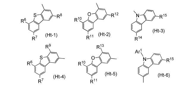
상기 일반식에 있어서, R6 내지 R15는 각각 독립적으로 수소, 탄소수 1 내지 6의 알킬기 또는 치환 또는 비치환의 페닐기 중 어느 하나를 나타낸다. 또한, Ar1은 치환 또는 비치환의 탄소수 1 내지 6의 알킬기, 또는 치환 또는 비치환의 페닐기 중 어느 하나를 나타낸다.In the general formulas, R 6 to R 15 each independently represent any one of hydrogen, an alkyl group having 1 to 6 carbon atoms, and a substituted or unsubstituted phenyl group. Ar 1 represents any of a substituted or unsubstituted alkyl group having 1 to 6 carbon atoms or a substituted or unsubstituted phenyl group.
또한, 본 발명의 다른 일 양태는 상기 구성을 갖는 화합물에 있어서, Htuni가 하기 일반식 (Ht-1) 내지 (Ht-3)으로 표시되는 기 중 어느 하나인 화합물이다.Further, another aspect of the invention is a compound of any one of the groups represented by the general formula (Ht-1) to (Ht-3) according to the, Ht uni the compound having the above configuration.
[일반식 (Ht-1) 내지 (Ht-3)][Formula (Ht-1) to (Ht-3)]

상기 일반식에 있어서, R6 내지 R15는 각각 독립적으로 치환 또는 비치환의 탄소수 1 내지 6의 알킬기 또는 치환 또는 비치환의 페닐기 중 어느 하나를 나타낸다.In the general formulas, R 6 to R 15 each independently represent a substituted or unsubstituted alkyl group having 1 to 6 carbon atoms or a substituted or unsubstituted phenyl group.
또한, 본 발명의 다른 일 양태는 상기 구성을 갖는 화합물에서, R6 내지 R15가 모두 수소인 화합물이다.Another embodiment of the present invention is a compound having the above structure, wherein R 6 to R 15 are all hydrogen.
또한, 본 발명의 다른 일 양태는 상기 구성을 갖는 화합물에서, R2 및 R4가 모두 수소인 화합물이다.Another embodiment of the present invention is a compound having the above structure, wherein R 2 and R 4 are both hydrogen.
또한, 본 발명의 다른 일 양태는 상기 구성을 갖는 화합물에서, R1 내지 R5가 모두 수소인 화합물이다.Another embodiment of the present invention is a compound having the above structure, wherein R 1 to R 5 are all hydrogen.
또한, 본 발명의 다른 일 양태는 하기 구조식 (100)으로 표시되는 화합물이다.Another embodiment of the present invention is a compound represented by the following structural formula (100).
[구조식 (100)][Structural formula (100)]

또한, 본 발명의 다른 일 양태는 상기 화합물을 포함하는 발광 소자용 재료이다.Another embodiment of the present invention is a light emitting device material comprising the above compound.
또한, 본 발명의 다른 일 양태는 한쌍의 전극과 한쌍의 전극 사이에 끼워진 EL층을 갖고, EL층은 상기 화합물을 포함하는 발광 소자이다.According to another aspect of the present invention, there is provided a light emitting device comprising an EL layer sandwiched between a pair of electrodes and a pair of electrodes, and the EL layer includes the above compound.
또한, 본 발명의 다른 일 양태는 한쌍의 전극과, 한쌍의 전극의 사이에 끼워진 EL층을 갖고, EL층은 적어도 발광 중심 물질을 포함하는 층을 갖고, 발광 중심 물질을 포함하는 층에 상기 화합물을 포함하는 발광 소자이다.According to another aspect of the present invention, there is provided a light emitting device comprising a pair of electrodes, an EL layer sandwiched between a pair of electrodes, an EL layer having a layer containing at least a luminescent center material, Emitting device.
또한, 본 발명의 다른 일 양태는 한쌍의 전극과, 한쌍의 전극의 사이에 끼워진 EL층을 갖고, EL층은 이리듐 착체와 상기 화합물을 포함하는 층을 갖는 발광 소자이다.Another embodiment of the present invention is a light emitting device having a pair of electrodes and an EL layer sandwiched between a pair of electrodes and the EL layer has a layer containing an iridium complex and the compound.
또한, 본 발명의 다른 일 양태는 상기 구성을 구비한 발광 소자를 갖는 디스플레이 모듈이다.According to another aspect of the present invention, there is provided a display module having a light emitting device having the above structure.
또한, 본 발명의 다른 일 양태는 상기 구성을 구비한 발광 소자를 갖는 조명 모듈이다.According to another aspect of the present invention, there is provided an illumination module having a light emitting device having the above-described structure.
또한, 본 발명의 다른 일 양태는 상기 구성을 구비한 발광 소자와 발광 소자를 제어하는 수단을 구비한 발광 장치이다.According to another aspect of the present invention, there is provided a light-emitting device including the light-emitting device having the above-described configuration and the means for controlling the light-emitting device.
또한, 본 발명의 다른 일 양태는 상기 구성을 구비한 발광 소자를 표시부에 갖고, 발광 소자를 제어하는 수단을 구비한 표시 장치이다.According to another aspect of the present invention, there is provided a display device including a light-emitting element having the above-described structure in a display portion, and means for controlling the light-emitting element.
또한, 본 발명의 다른 일 양태는 상기 구성을 구비한 발광 소자를 조명부에 갖고, 발광 소자를 제어하는 수단을 구비한 조명 장치이다.According to another aspect of the present invention, there is provided a lighting apparatus having a light-emitting element having the above-described configuration in an illumination section and having means for controlling the light-emitting element.
또한, 본 발명의 다른 일 양태는 상기 구성을 구비한 발광 소자를 갖는 전자 기기이다.According to another aspect of the present invention, there is provided an electronic device having a light emitting element having the above-described structure.
본 발명의 일 양태에 따른 발광 소자는 발광 효율이 양호한 발광 소자이다. 또한, 구동 전압이 낮은 발광 소자이다. 또한, 발광 효율이 양호한 녹색 내지 청색의 영역의 발광을 나타내는 발광 소자이다.A light emitting device according to an embodiment of the present invention is a light emitting device having a good light emitting efficiency. Further, it is a light emitting element having a low driving voltage. Further, it is a light-emitting element exhibiting light emission in a green to blue region with good light-emitting efficiency.
본 발명의 일 양태에 따른 헤테로환 화합물은 큰 에너지 갭을 가진다. 또한, 뛰어난 캐리어 수송성을 가진다. 따라서, 발광 소자의 수송층을 구성하는 재료나 발광층에서의 호스트 재료, 발광 중심 물질로서 적합하게 이용하는 것이 가능하다.The heterocyclic compound according to one embodiment of the present invention has a large energy gap. In addition, it has excellent carrier transportability. Therefore, it is possible to suitably use the material constituting the transport layer of the light emitting element, the host material in the light emitting layer, and the luminescent center material.
또한, 본 발명의 다른 일 양태에서는 상기 헤테로환 화합물을 이용한 소비 전력이 작은 디스플레이 모듈, 조명 모듈, 발광 장치, 조명 장치, 표시 장치 및 전자 기기를 각각 제공할 수 있다. 또는, 신규 발광 소자, 신규 발광 장치 등을 제공할 수 있다. 또한, 이러한 효과의 기재는 다른 효과의 존재를 방해하는 것은 아니다. 또한, 본 발명의 일 양태는 반드시 이러한 효과를 전부 가질 필요는 없다. 또한, 이것들 이외의 효과는 명세서, 도면, 청구항 등의 기재로부터 저절로 분명해지는 것이며, 명세서, 도면, 청구항 등의 기재로부터 이것들 이외의 효과를 추출하는 것이 가능하다.In another embodiment of the present invention, a display module, an illumination module, a light emitting device, a lighting device, a display device, and an electronic device each having a small power consumption using the heterocyclic compound may be provided. Alternatively, a novel light emitting device, a novel light emitting device, and the like can be provided. Also, the description of such an effect does not preclude the presence of other effects. In addition, one aspect of the present invention does not necessarily have all of these effects. The effects other than these are obviously made clear from the description of the specification, the drawings, the claims, and the like, and it is possible to extract other effects from the description of the specification, the drawings, the claims, and the like.
도 1은 발광 소자의 개념도.
도 2는 액티브 매트릭스형 발광 장치의 개념도.
도 3은 액티브 매트릭스형 발광 장치의 개념도.
도 4는 액티브 매트릭스형 발광 장치의 개념도.
도 5는 패시브 매트릭스형 발광 장치의 개념도.
도 6은 전자 기기를 나타내는 도면.
도 7은 광원 장치를 나타내는 도면.
도 8은 조명 장치를 나타내는 도면.
도 9는 조명 장치 및 전자 기기를 나타내는 도면.
도 10은 차량 탑재 표시 장치 및 조명 장치를 나타내는 도면.
도 11은 전자 기기를 나타내는 도면.
도 12는 4mDBTBPBfpm-II의 NMR 차트.
도 13은 4mDBTBPBfpm-II의 흡수 스펙트럼 및 발광 스펙트럼.
도 14는 4mDBTBPBfpm-II의 LC/MS 분석 결과.
도 15는 발광 소자 1의 전류 밀도-휘도 특성.
도 16은 발광 소자 1의 전압-휘도 특성.
도 17은 발광 소자 1의 휘도-전류 효율 특성.
도 18은 발광 소자 1의 휘도-외부 양자 효율 특성.
도 19는 발광 소자 1의 휘도-파워 효율 특성.
도 20은 발광 소자 1의 발광 스펙트럼.
도 21은 발광 소자 1의 정규화 휘도 시간 변화 특성.
도 22는 발광 소자 2의 전류 밀도-휘도 특성.
도 23은 발광 소자 2의 전압-휘도 특성.
도 24는 발광 소자 2의 휘도-전류 효율 특성.
도 25는 발광 소자 2의 휘도-외부 양자 효율 특성.
도 26은 발광 소자 2의 휘도-파워 효율 특성.
도 27은 발광 소자 2의 발광 스펙트럼.
도 28은 발광 소자 2의 정규화 휘도 시간 변화 특성.1 is a conceptual view of a light emitting device;
2 is a conceptual view of an active matrix light emitting device.
3 is a conceptual view of an active matrix light emitting device.
4 is a conceptual diagram of an active matrix type light emitting device.
5 is a conceptual view of a passive matrix type light emitting device.
6 is a view showing an electronic device;
7 is a view showing a light source device.
8 is a view showing a lighting device.
9 is a view showing a lighting device and an electronic device.
10 is a view showing a vehicle-mounted display device and a lighting device.
11 is a view showing an electronic device.
12 is an NMR chart of 4mDBTBPBfpm-II.
13 shows the absorption spectrum and emission spectrum of 4mDBTBPBfpm-II.
14 shows LC / MS analysis results of 4mDBTBPBfpm-II.
15 is a current density-luminance characteristic of the light-emitting
16 is a voltage-luminance characteristic of the light-emitting
17 shows luminance-current efficiency characteristics of the light-emitting
18 shows luminance-external quantum efficiency characteristics of the light-emitting
19 shows luminance-power efficiency characteristics of the light-emitting
20 shows the emission spectrum of the light-emitting
21 shows the normalized luminance time change characteristics of the
22 shows current density-luminance characteristics of the light-emitting
23 shows voltage-luminance characteristics of the light-emitting
24 shows luminance-current efficiency characteristics of the light-emitting
25 shows the luminance-external quantum efficiency characteristic of the light-emitting
26 shows the luminance-power efficiency characteristic of the light-emitting
27 shows the emission spectrum of the light-emitting
28 shows the normalized luminance time change characteristics of the
이하, 본 발명의 실시형태에 대하여 설명한다. 단, 본 발명은 많은 다른 양태로 실시하는 것이 가능하고, 본 발명의 취지 및 그 범위로부터 벗어나지 않고 그 형태 및 상세한 사항을 다양하게 변경할 수 있다는 것은 당업자라면 용이하게 이해할 수 있다. 따라서, 본 실시형태의 기재 내용에 한정하여 해석되는 것은 아니다.Hereinafter, an embodiment of the present invention will be described. It will be apparent to those skilled in the art, however, that the present invention may be embodied with many other modes, and that various changes in form and details may be made therein without departing from the spirit and scope of the present invention. Therefore, the present invention is not limited to the description of the present embodiment.
또한, "막"이라는 말과 "층"이라는 말은, 경우에 따라, 또는, 상황에 따라, 서로 바꿀 수 있다. 예를 들면, "도전층"이라는 용어를 "도전막"이라는 용어로 변경하는 것이 가능한 경우가 있다. 또는, 예를 들면, "절연막"이라는 용어를 "절연층"이라는 용어로 변경하는 것이 가능한 경우가 있다.In addition, the words "membrane" and "layer" may be interchanged, depending on circumstances or circumstances. For example, it is sometimes possible to change the term "conductive layer" to the term "conductive film ". Alternatively, for example, it is sometimes possible to change the term "insulating film" to the term "insulating layer".
(실시형태 1)(Embodiment 1)
본 실시형태에 설명하는 본 발명의 일 양태의 화합물은 벤조티에노피리미딘 골격을 갖는 물질이다. 상기 골격을 갖는 화합물은 캐리어(특히 전자)의 수송성이 우수하다. 이로 인하여, 구동 전압이 낮은 발광 소자를 제공할 수 있다.The compound of one embodiment of the present invention described in this embodiment is a substance having a benzothienopyrimidine skeleton. The compound having a skeleton is excellent in transportability of a carrier (particularly, an electron). As a result, a light emitting device having a low driving voltage can be provided.
또한, 상기 화합물은 높은 삼중항 여기 준위(T1 준위)를 갖는 화합물로 할 수 있다. 따라서, 인광을 발하는 발광 중심 물질을 이용한 발광 소자에 적합하게 이용할 수 있다. 구체적으로는, 상기 화합물이 높은 삼중항 여기 준위(T1 준위)를 가지면, 인광 발광 물질의 여기 에너지가 이동하게 되는 것을 억제할 수 있기 때문에, 여기 에너지를 효과적으로 발광으로 변환할 수 있다. 인광 발광 물질로서는, 이리듐 착체가 대표적이다.In addition, the compound may be a compound having a high triplet excitation level (T 1 level). Therefore, it can be suitably used for a light emitting device using a luminescent center material emitting phosphorescence. Specifically, when the compound has a high triplet excitation level (T 1 level), the excitation energy of the phosphorescent light-emitting substance can be inhibited from shifting, so that excitation energy can be effectively converted into light emission. As the phosphorescent material, an iridium complex is typical.
또한, 벤조티에노피리미딘 골격으로서는, 구체적으로는 벤조티에노[3,2-d]피리미딘 골격 등을 들 수 있지만, 이것에 한정되지 않는다.Specific examples of the benzothienopyrimidine skeleton include, but are not limited to, a benzothieno [3,2- d ] pyrimidine skeleton.
상기 벤조티에노피리미딘 골격을 갖는 화합물의 바람직한 구체적인 예를 하기 일반식 (G1)로 나타낸다.Specific preferred examples of the compound having a benzothienopyrimidine skeleton are represented by the following general formula (G1).
[일반식 (G1)][General formula (G1)]

식 중 A1은 탄소수 6 내지 100의 아릴기를 나타낸다. 단, A1에는 헤테로 방향환이 포함되어 있어도 좋다.In the formula, A 1 represents an aryl group having 6 to 100 carbon atoms. However, A 1 may contain a hetero aromatic ring.
상기 탄소수 6 내지 100의 아릴기로서는, 대표적으로는 하기 일반식 (A1-1) 내지 (A1-6)로 표시되는 기를 들 수 있다. 또한, 이하는 어디까지나 대표예이며 탄소수 6 내지 100의 아릴기는 이것들에 한정되지 않는다.Examples of the aryl group having 6 to 100 carbon atoms include groups represented by the following general formulas (A 1 -1) to (A 1 -6). The following are representative examples, and the aryl groups having 6 to 100 carbon atoms are not limited to these.
[일반식 (A1-1) 내지 (A1-6)][Formula (A 1 -1) to (A 1 -6)]
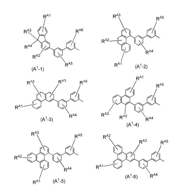
식 중 RA1 내지 RA6은 각각 독립적으로 수소 또는 치환 또는 비치환의 탄소수 1 내지 6의 알킬기, 치환 또는 비치환의 탄소수 5 내지 7의 단환식 포화 탄화 수소, 치환 또는 비치환의 탄소수 7 내지 10의 다환식 포화 탄화 수소, 또는 치환 또는 비치환의 탄소수 6 내지 13의 아릴기를 나타낸다. 또한, RA1 내지 RA6이 방향족환에 결합하고 있을 때, 이 방향족환에서 가능한 치환수의 범위에서, 각각 1 내지 4의 치환기를 나타낸다.Wherein R A1 to R A6 each independently represent hydrogen or a substituted or unsubstituted alkyl group having 1 to 6 carbon atoms, a substituted or unsubstituted monocyclic saturated hydrocarbon having 5 to 7 carbon atoms, a substituted or unsubstituted polycyclic group having 7 to 10 carbon atoms Saturated hydrocarbon, or substituted or unsubstituted aryl group having 6 to 13 carbon atoms. When R A1 to R A6 are bonded to an aromatic ring, they each represent a substituent of 1 to 4 in the range of substitution possible in the aromatic ring.
또한, 헤테로 방향환을 포함하는 A1로서는, 대표적으로는 하기 일반식 (A1-10) 내지 (A1-25)로 표시되는 기를 들 수 있다. 또한, 이하는 어디까지나 대표예이며 A1은 예시에 한정되지 않는다.Examples of A 1 containing heteroaromatic rings include groups represented by the following general formulas (A 1 -10) to (A 1 -25). The following is a representative example only, and A 1 is not limited to the example.
[일반식 (A1-10) 내지 (A1-25)][Formula (A 1 -10) to (A 1 -25)]


또한, R1 내지 R5는 각각 독립적으로 수소 또는 치환 또는 비치환의 탄소수 1 내지 6의 알킬기, 치환 또는 비치환의 탄소수 5 내지 7의 단환식 포화 탄화 수소, 치환 또는 비치환의 탄소수 7 내지 10의 다환식 포화 탄화 수소, 또는 치환 또는 비치환의 탄소수 6 내지 13의 아릴기를 나타낸다.Each of R 1 to R 5 independently represents hydrogen, a substituted or unsubstituted alkyl group having 1 to 6 carbon atoms, a substituted or unsubstituted monocyclic saturated hydrocarbon having 5 to 7 carbon atoms, a substituted or unsubstituted polycyclic group having 7 to 10 carbon atoms Saturated hydrocarbon, or substituted or unsubstituted aryl group having 6 to 13 carbon atoms.
또한, R1 내지 R5에서의 비치환의 탄소수 1 내지 6의 알킬기의 구체적인 예로서는, 메틸기, 에틸기, 프로필기, 아아이소프로필기, 부틸기, sec-부틸기, 아이소부틸기, tert-부틸기, 펜틸기, 아이소펜틸기, sec-펜틸기, tert-펜틸기, 네오펜틸기, 헥실기, 아이소헥실기, sec-헥실기, tert-헥실기, 네오헥실기, 3-메틸펜틸기, 2-메틸펜틸기, 2-에틸부틸기, 1,2-다이메틸부틸기, 2,3-다이메틸부틸기 등을 들 수 있고, 비치환의 탄소수 5 내지 7의 단환식 포화 탄화 수소의 구체적인 예로서는, 사이클로 프로필기, 사이클로부틸기, 사이클로펜틸기, 사이클로헥실기, 사이클로옥틸기, 2-메틸사이클로헥실기, 2,6-다이메틸사이클로헥실기 등을 들 수 있고, 비치환의 탄소수 7 내지 10의 다환식 포화 탄화 수소의 구체적인 예로서는, 데카하이드로나프틸기, 아다만틸기를 들 수 있고, 비치환의 탄소수 6 내지 13의 아릴기의 구체적인 예로서는, 페닐기, o-톨릴기, m-톨릴기, p-톨릴기, 메시틸기, o-바이페닐기, m-바이페닐기, p-바이페닐기, 1-나프틸기, 2-나프틸기, 플루오레닐기, 9,9-다이메틸플루오레닐기를 들 수 있다.In addition, R 1 to R 5 Specific examples of the unsubstituted alkyl group having 1 to 6 carbon atoms in the methyl group, an ethyl group, a propyl group, an O-isopropyl group, a butyl group, sec- butyl group, isobutyl group, tert - butyl, pentyl, iso-pentyl, sec - pentyl, tert - pentyl group, a neopentyl group, a hexyl group, iso-hexyl, sec - hexyl group, a tert - hexyl, neo-hexyl, 3-methyl pentyl group, 2- Methylbutyl group, 2-ethylbutyl group, 1,2-dimethylbutyl group, 2,3-dimethylbutyl group and the like, and specific examples of unsubstituted monocyclic saturated hydrocarbons having 5 to 7 carbon atoms include cyclo Propyl group, cyclobutyl group, cyclopentyl group, cyclohexyl group, cyclooctyl group, 2-methylcyclohexyl group, 2,6-dimethylcyclohexyl group and the like, and unsubstituted polycyclic Concrete examples of saturated hydrocarbons include decahydronaphthyl group and adamantyl group Specific examples of the unsubstituted aryl group having 6 to 13 carbon atoms include a phenyl group, o-tolyl group, m-tolyl group, p-tolyl group, mesityl group, o- Naphthyl group, fluorenyl group, and 9,9-dimethylfluorenyl group.
R1 내지 R5에 대하여, 이것들이 치환기를 더 갖는 경우, 상기 치환기로서는 탄소수 1 내지 3의 알킬기로 대표되는 특성에 큰 변화를 미치지 않는 기를 상정하고 있다.When R 1 to R 5 further have a substituent, the substituent is a group which does not significantly change the characteristics represented by the alkyl group having 1 to 3 carbon atoms.
또한, 본 실시형태에 설명하는 벤조티에노피리미딘에 대하여, 더 바람직한 구체적인 예는 하기 일반식 (G2)로 표시할 수 있다.Further specific examples of benzothienopyrimidines described in this embodiment can be represented by the following general formula (G2).
[일반식 (G2)][General formula (G2)]

식 중, R1 내지 R5에 대해서는, 상기 일반식 (G1)에서의 R1 내지 R5와 마찬가지이므로, 중복하는 기재를 생략한다. 일반식 (G1)에서의 R1 내지 R5의 기재를 참조하기 바란다.For, R 1 to R 5 in the formula, because it is the same as R 1 to R 5 in the general formula (G1), will be omitted for redundancy. Please refer to the description of R 1 to R 5 in the general formula (G1).
상기 일반식 (G2) 중, α는 치환 또는 비치환의 페닐렌기를 나타내고, n은 0 내지 4의 정수(整數)를 나타낸다. α에 대하여, 이것들이 치환기를 더 갖는 경우, 상기 치환기로서는 탄소수 1 내지 3의 알킬기로 대표되는 화합물의 특성에 큰 변화를 미치지 않는 기를 상정하고 있다.In the general formula (G2),? Represents a substituted or unsubstituted phenylene group, and n represents an integer of 0 to 4. a group which does not cause a significant change in the characteristics of the compound represented by the alkyl group having 1 to 3 carbon atoms is considered as the above substituent when these have a substituent.
또한, Htuni와 벤조티에노피리미딘 골격의 상호 작용을 억제하여, 높은 삼중항 여기 준위(T1 준위)를 유지하는 관점에서, n은 1 이상인 것이 바람직하고, 열물성이 향상되어 분자의 안정성이 좋아진다는 관점에서, 보다 바람직한 n의 구성은 2이다. 또한, n이 2인 경우, α와 n으로 표시되는 2가의 기는 1,1'-바이페닐-3,3'-다이일기인 것이 바람직하다.From the viewpoint of inhibiting the interaction between Ht uni and the benzothienopyrimidine skeleton and maintaining a high triplet excitation level (T 1 level), it is preferable that n is 1 or more, and the thermal properties are improved, From the viewpoint of improving the performance, the configuration of n is more preferable. When n is 2, it is preferable that the divalent group represented by? And n is a 1,1'-biphenyl-3,3'-diyl group.
또한, 상기 일반식 (G2) 중 Htuni는 정공 수송성을 갖는 골격을 나타낸다. Htuni로서는, 높은 삼중항 여기 준위(T1 준위)를 유지하는 관점에서, 치환 또는 비치환의 다이벤조티오페닐기, 치환 또는 비치환의 다이벤조퓨라닐기, 치환 또는 비치환의 카바졸일기를 이용하는 것이 바람직하다. 또한, 이것들이 치환기를 갖는 경우, 상기 치환기로서는 탄소수 1 내지 3의 알킬기로 대표되는 특성에 큰 변화를 미치지 않는 기를 상정하고 있다.In the general formula (G2), Ht uni represents a skeleton having hole transportability. As Ht uni, it is preferred to use from the viewpoint of maintaining a high triplet excitation level (T 1 level), a substituted or unsubstituted dibenzo thiophenyl group, a substituted or unsubstituted dibenzo furanoid group, a substituted or unsubstituted carbazole group . In addition, when they have a substituent, the substituent is a group which does not significantly change the characteristics represented by the alkyl group having 1 to 3 carbon atoms.
Htuni의 구체적인 예로서는, 하기 일반식 (Ht-1) 내지 (Ht-6)로 표시되는 기는 합성이 용이하고, 바람직한 예이다. 또한, 물론, Htuni는 이하의 예시에 한정되는 것은 아니다.Specific examples include groups represented by the following general formula (Ht-1) to (Ht-6) of the uni Ht synthesis is easy, and is a preferred example. Of course, Ht uni is not limited to the following examples.
[일반식 (Ht-1) 내지 (Ht-6)][Formula (Ht-1) to (Ht-6)]

R6 내지 R15는 각각 독립적으로 수소 또는 치환 또는 비치환의 탄소수 1 내지 6의 알킬기 또는 치환 또는 비치환의 페닐기 중 어느 하나를 나타낸다. 또한, Ar1은 탄소수 1 내지 6의 알킬기, 치환 또는 비치환의 페닐기 중 어느 하나를 나타낸다. 또한, 이것들이 치환기를 갖는 경우, 상기 치환기로서는 탄소수 1 내지 3의 알킬기로 대표되는 특성에 큰 변화를 미치지 않는 기를 상정하고 있다.Each of R 6 to R 15 independently represents hydrogen, a substituted or unsubstituted alkyl group having 1 to 6 carbon atoms, or a substituted or unsubstituted phenyl group. Ar 1 represents any one of an alkyl group having 1 to 6 carbon atoms and a substituted or unsubstituted phenyl group. In addition, when they have a substituent, the substituent is a group which does not significantly change the characteristics represented by the alkyl group having 1 to 3 carbon atoms.
또한, 상기 일반식 (Ht-1) 내지 (Ht-3)으로 표시되는 기는 높은 삼중항 여기 준위(T1 준위)를 갖고, 또한 정공 수송성을 가지기 때문에, 바람직한 구성이다. 또한, (Ht-1) 내지 (Ht-3)는 벤조티에노피리미딘 골격과의 조합에서는 전자 도너 부위로서 기능한다(벤조티에노피리미딘이 전자 억셉터 부위로서 기능함). 그러므로 막의 전하 수송에 주목한 경우, 벌크에서는 도전율이, 계면에서는 주입성이 향상되어 저전압 구동이 가능하게 되기 때문에 발광 소자에서 바람직한 구성이다.The groups represented by the general formulas (Ht-1) to (Ht-3) are preferred because they have a high triplet excitation level (T 1 level) and also have hole transportability. In addition, (Ht-1) to (Ht-3) function as an electron donor site in combination with a benzothienopyrimidine skeleton (benzothienopyrimidine functions as an electron acceptor site). Therefore, when paying attention to the charge transport of the film, the conductivity is improved in the bulk and the injection property is improved at the interface, and low-voltage driving becomes possible, which is a preferable constitution in the light emitting device.
또한, 상기 일반식 (Ht-1) 내지 (Ht-6)로 표시되는 기에서 R6 내지 R15가 모두 수소인 구성이, 원료의 조달이나 합성이 용이하고 바람직한 구성이다.In the groups represented by the general formulas (Ht-1) to (Ht-6), all of R 6 to R 15 are hydrogen is a preferable structure because it is easy to procure or synthesize raw materials.
또한, 같은 이유에 의해, 상기 일반식 (G2)로 표시되는 화합물에서, R2 및 R4가 모두 수소인 구성이 바람직하다. 또한, R1 내지 R5가 모두 수소인 구성이 바람직하다.For the same reason, it is preferable that in the compound represented by the general formula (G2), R 2 and R 4 are all hydrogen. It is also preferable that all of R 1 to R 5 are hydrogen.
또한, 본 실시형태에 설명하는 벤조티에노피리미딘에 대하여, 더욱 바람직한 구체적인 예는 하기 일반식 (G3)으로 표시할 수 있다.A more preferable specific example of benzothienopyrimidine described in this embodiment can be represented by the following general formula (G3).
[일반식 (G3)][General formula (G3)]

식 중, R1 내지 R5에 대해서는, 상기 일반식 (G1)에서의 R1 내지 R5와 마찬가지이므로, 중복하는 기재를 생략한다. 일반식 (G1)에서의 R1 내지 R5의 기재를 참조하기 바란다. 또한, 식 중, Htuni에 대해서는, 상기 일반식 (G2)의 Htuni와 마찬가지이므로, 중복하는 기재를 생략한다. 일반식 (G2)에서의 Htuni의 기재를 참조하기 바란다.For, R 1 to R 5 in the formula, because it is the same as R 1 to R 5 in the general formula (G1), will be omitted for redundancy. Please refer to the description of R 1 to R 5 in the general formula (G1). With respect to, uni wherein Ht, Ht so uni Like the above general formula (G2), is omitted for redundancy. Please refer to the description of Ht uni in the general formula (G2).
상술한 화합물의 대표적인 예를 이하에 나타낸다. 또한, 본 실시형태에 설명하는 화합물은 이하의 예시에 의해 한정되는 것은 아니다.Representative examples of the above-mentioned compounds are shown below. The compounds described in this embodiment are not limited by the following examples.


이상과 같은 화합물은 캐리어의 수송성이 우수하기 때문에 캐리어 수송 재료나 호스트 재료로서 적합하다. 이것에 의해, 구동 전압이 낮은 발광 소자를 제공할 수도 있다. 또한, 높은 삼중항 여기 준위(T1 준위)를 갖는 화합물로 할 수 있기 때문에, 발광 효율이 높은 인광 발광 소자를 얻을 수 있다. 특히, 녹색보다 단파장측에 발광의 피크를 갖는 인광 발광 소자에서도, 양호한 발광 효율을 갖는 발광 소자를 제공하는 것이 가능하게 된다. 또한, 높은 삼중항 여기 준위(T1 준위)를 가진다는 것은 또한 큰 밴드 갭을 가진다는 것을 의미하므로, 청색 형광을 나타내는 발광 소자도 효율적으로 발광시킬 수 있다.The above compound is suitable as a carrier transporting material and a host material because of excellent carrier transportability. Thus, a light emitting element having a low driving voltage can be provided. Further, since a compound having a high triplet excitation level (T 1 level) can be obtained, a phosphorescent device having a high luminous efficiency can be obtained. Particularly, even in a phosphorescent light emitting element having a peak of light emission on the shorter wavelength side than green, it becomes possible to provide a light emitting element having a good luminous efficiency. Further, having a high triplet excitation level (T 1 level) also means that it has a large bandgap, so that a light emitting device exhibiting blue fluorescence can also efficiently emit light.
계속하여, 상기 일반식 (G1)로 표시되는 화합물의 합성 방법에 대하여 설명한다.Next, a method for synthesizing the compound represented by the general formula (G1) will be described.
일반식 (G1)로 표시되는 화합물은 이하와 같이 간편한 합성 스킴에 의해 합성할 수 있다. 예를 들면, 하기 합성 스킴 (a)에 나타내는 바와 같이, 벤조티에노피리미딘 유도체의 할로겐 화합물(A1)과 아릴기 A1의 보론산 화합물(A2)을 반응시킴으로써 얻을 수 있다. 또한, 식 중 X는 할로겐 원소를 나타낸다. 또한, B1은 보론산 또는 보론산 에스터 또는 환상 트리올 보레이트염 등을 나타낸다. 환상 트리올 보레이트염은 리튬염 외에, 칼륨염, 나트륨염을 이용해도 좋다.The compound represented by the general formula (G1) can be synthesized by a simple synthesis scheme as follows. Can be obtained, for example, by reacting a halogen compound (A1) of a benzothienopyrimidine derivative with a boronic acid compound (A2) of an aryl group A 1 as shown in the following synthesis scheme (a). In the formula, X represents a halogen element. In addition, B 1 represents a boronic acid or a boronic acid ester or a cyclic triol borate salt. The cyclic triol borate salt may be a potassium salt or a sodium salt in addition to a lithium salt.
[합성 스킴 (a)][Synthesis Scheme (a)]

또한, 합성 스킴 (a)에서, X는 할로겐을 나타내고, A1은 아릴기이다. 단, A1에는 헤테로 방향환이 포함되어 있어도 좋다. 또한, R1 내지 R5는 각각 독립적으로 수소 또는 치환 또는 비치환의 탄소수 1 내지 6의 알킬기, 치환 또는 비치환의 탄소수 5 내지 7의 단환식 포화 탄화 수소, 치환 또는 비치환의 탄소수 7 내지 10의 다환식 포화 탄화 수소, 치환 또는 비치환의 탄소수 6 내지 13의 아릴기 중 어느 하나를 나타낸다.Also, in the synthetic scheme (a), X represents a halogen and A 1 represents an aryl group. However, A 1 may contain a hetero aromatic ring. Each of R 1 to R 5 independently represents hydrogen, a substituted or unsubstituted alkyl group having 1 to 6 carbon atoms, a substituted or unsubstituted monocyclic saturated hydrocarbon having 5 to 7 carbon atoms, a substituted or unsubstituted polycyclic group having 7 to 10 carbon atoms A saturated hydrocarbon group, and a substituted or unsubstituted aryl group having 6 to 13 carbon atoms.
또한, 벤조티에노피리미딘 유도체의 보론산 화합물과 아릴기 A1의 할로겐 화합물을 반응시켜도 좋다.The boronic acid compound of the benzothienopyrimidine derivative and the halogen compound of the aryl group A 1 may be reacted.
상술한 화합물 (A1), (A2)는 다양한 종류가 시판되고 있거나, 혹은 합성 가능하기 때문에, 일반식 (G1)로 표시되는 화합물은 수많은 종류를 합성할 수 있다. 따라서, 본 발명의 화합물은 베리에이션(variation)이 풍부하다는 특징이 있다.Since various kinds of the above-mentioned compounds (A1) and (A2) are commercially available or can be synthesized, a number of kinds of compounds represented by the general formula (G1) can be synthesized. Therefore, the compound of the present invention is characterized by abundant variation.
이상, 본 발명의 일 양태인 화합물의 합성 방법의 일례에 대하여 설명했지만, 본 발명은 이에 한정되는 것은 아니고, 다른 어떠한 합성 방법에 의해 합성되어도 좋다.As described above, an example of the method of synthesizing the compound of one embodiment of the present invention has been described. However, the present invention is not limited to this and may be synthesized by any other synthesis method.
또한, 본 실시형태에서, 본 발명의 일 양태에 대하여 설명했다. 또는, 다른 실시형태에서, 본 발명의 일 양태에 대하여 설명한다. 단, 본 발명의 일 양태는 이것들에 한정되지 않는다. 예를 들면, 본 발명의 일 양태로서 벤조티에노피리미딘 골격을 갖는 경우의 예를 나타냈지만, 본 발명의 일 양태는 이것으로 한정되지 않는다. 경우에 따라, 또는, 상황에 따라, 본 발명의 일 양태는 벤조티에노피리미딘 골격 이외의 골격을 갖고 있어도 좋다. 예를 들면, 경우에 따라, 또는, 상황에 따라, 본 발명의 일 양태는 벤조티에노피리미딘 골격 이외의 골격을 갖지 않아도 좋다.In the present embodiment, one aspect of the present invention has been described. In another embodiment, an aspect of the present invention will be described. However, one aspect of the present invention is not limited to these. For example, an example in which the benzothienopyrimidine skeleton is present as one embodiment of the present invention is shown, but one aspect of the present invention is not limited thereto. Optionally, or depending on the circumstances, one embodiment of the present invention may have a skeleton other than a benzothienopyrimidine skeleton. For example, in some cases, or depending on the circumstances, one embodiment of the present invention may not have a skeleton other than a benzothienopyrimidine skeleton.
(실시형태 2)(Embodiment 2)
본 실시형태에서는, 벤조티에노피리미딘 골격을 포함하는 화합물을 갖는 발광 소자의 일 양태에 대하여 도 1의 (A)을 이용하여 이하에 설명한다.In this embodiment mode, one embodiment of a light emitting device having a compound having a benzothienopyrimidine skeleton will be described below with reference to Fig. 1 (A).
본 실시형태에서의 발광 소자는 한쌍의 전극 사이에 복수의 층을 가진다. 본 형태에서, 발광 소자는 제1 전극(101)과, 제2 전극(102)과, 제1 전극(101)과 제2 전극(102) 사이에 제공된 EL층(103)으로 구성되어 있다. 또한, 도 1의 (A)에서는 제1 전극(101)은 양극으로서 기능하고, 제2 전극(102)은 음극으로서 기능하는 것으로서 도시한다. 즉, 제1 전극(101)이 제2 전극(102)보다 전위가 높아지도록, 제1 전극(101)과 제2 전극(102)에 전압을 인가했을 때, 발광이 얻어지는 구성으로 되어 있다. 물론, 제1 전극이 음극으로서 기능하고, 제2 전극이 양극으로서 기능해도 상관없다. 그 경우, EL층의 적층 순서는 이하에 설명하는 순서와 반대가 된다. 또한, 본 실시형태에서의 발광 소자는 EL층(103)의 어느 한 층에 벤조티에노피리미딘 골격을 갖는 화합물이 포함되어 있으면 좋다. 또한, 벤조티에노피리미딘 골격을 갖는 화합물이 포함되는 층으로서는, 발광층이나 전자 수송층이 상기 화합물의 특성을 보다 살릴 수 있어, 양호한 특성을 갖는 발광 소자를 얻을 수 있기 때문에 바람직하다.The light emitting element in this embodiment has a plurality of layers between a pair of electrodes. In this embodiment, the light emitting element is composed of the
양극으로서 기능하는 전극으로서는, 일 함수가 큰(구체적으로는 4.0 eV 이상), 금속, 합금, 도전성 화합물, 및 이들의 혼합물 등을 이용하는 것이 바람직하다. 구체적으로는, 예를 들면, 인듐 주석 산화물(ITO:Indium Tin Oxide), 규소 혹은 산화 규소를 함유한 인듐 주석 산화물, 산화 인듐-산화 아연, 산화 텅스텐 및 산화 아연을 함유한 산화 인듐(IWZO) 등을 들 수 있다. 이러한 도전성 금속 산화물막은 통상 스퍼터링법에 의해 성막되지만, 졸-겔법 등을 응용하여 제작해도 상관없다. 예를 들면, 산화 인듐-산화 아연은 산화 인듐에 대하여 1 wt% 이상 20 wt% 이하의 산화 아연을 더한 타겟을 이용하여 스퍼터링법에 의해 형성할 수 있다. 또한, 산화 텅스텐 및 산화 아연을 함유한 산화 인듐(IWZO)은 산화 인듐에 대하여 산화 텅스텐을 0.5wt% 이상 5 wt% 이하, 산화 아연을 0.1wt% 이상 1 wt% 이하 함유한 타겟을 이용하여 스퍼터링법에 의해 형성할 수 있다. 이 외에, 금(Au), 백금(Pt), 니켈(Ni), 텅스텐(W), 크롬(Cr), 몰리브덴(Mo), 철(Fe), 코발트(Co), 구리(Cu), 팔라듐(Pd), 또는 금속 재료의 질화물(예를 들면, 질화 티탄) 등을 들 수 있다. 또한, 그라펜을 이용해도 좋다.As the electrode functioning as the anode, it is preferable to use a metal having a large work function (specifically, 4.0 eV or more), an alloy, a conductive compound, a mixture thereof, or the like. Specifically, for example, indium tin oxide (ITO), indium tin oxide containing silicon or silicon oxide, indium oxide (IWZO) containing indium oxide-zinc oxide, tungsten oxide and zinc oxide, etc. . Such a conductive metal oxide film is usually formed by a sputtering method, but it may be manufactured by applying a sol-gel method or the like. For example, the indium oxide-zinc oxide can be formed by a sputtering method using a target in which 1 wt% to 20 wt% of zinc oxide is added to indium oxide. Indium oxide (IWZO) containing tungsten oxide and zinc oxide is sputtered using a target containing tungsten oxide in an amount of 0.5 wt% to 5 wt% and indium oxide in an amount of 0.1 wt% to 1 wt% Can be formed by a method. (Au), platinum (Pt), nickel (Ni), tungsten (W), chromium (Cr), molybdenum (Mo), iron (Fe), cobalt Pd), or a nitride of a metal material (e.g., titanium nitride). Also, graphene may be used.
EL층(103)의 적층 구조에 대해서는 특별히 한정되지 않고, 전자 수송성이 높은 물질을 포함하는 층 또는 정공 수송성이 높은 물질을 포함하는 층, 전자 주입성이 높은 물질을 포함하는 층, 정공 주입성이 높은 물질을 포함하는 층, 바이폴러성(전자 및 정공의 수송성이 높은 물질)의 물질을 포함하는 층, 캐리어 블록성을 갖는 층 등을 적절히 조합하여 구성하면 좋다. 본 실시형태에서는, EL층(103)은 양극으로서 기능하는 전극측으로부터 "정공 주입층(111), 정공 수송층(112), 발광층(113), 전자 수송층(114), 전자 주입층(115)"의 순으로 적층한 구성을 갖는 것으로서 설명한다. 각 층을 구성하는 재료에 대하여 이하에 구체적으로 나타낸다.The layer structure of the
정공 주입층(111)은 정공 주입성의 물질을 포함하는 층이다. 몰리브덴 산화물이나 바나듐 산화물, 루테늄 산화물, 텅스텐 산화물, 망간 산화물 등을 이용할 수 있다. 이 외에, 프탈로시아닌(약칭:H2Pc)이나 구리 프탈로시아닌(CuPC) 등의 프탈로시아닌계의 화합물, 4,4'-비스[N-(4-다이페닐아미노페닐)-N-페닐아미노]바이페닐(약칭:DPAB), N,N'-비스{4-[비스(3-메틸페닐)아미노]페닐}-N,N'-다이페닐-(1,1'-바이페닐)-4,4'-다이아민(약칭:DNTPD) 등의 방향족 아민 화합물, 혹은 폴리(에틸렌다이옥시티오펜)/폴리(스티렌설폰산)(PEDOT/PSS) 등의 고분자 등에 의해도 정공 주입층(111)을 형성할 수 있다.The hole injection layer 111 is a layer containing a hole injection material. Molybdenum oxide, vanadium oxide, ruthenium oxide, tungsten oxide, manganese oxide and the like can be used. In addition, phthalocyanine compounds such as phthalocyanine (abbreviated as H 2 Pc) and copper phthalocyanine (CuPC), 4,4'-bis [N- (4-diphenylaminophenyl) (DPAB), N, N'-bis {4- [bis (3-methylphenyl) amino] phenyl} -N, N'- diphenyl- (1,1'- The hole injecting layer 111 can also be formed by an aromatic amine compound such as poly (ethylene dioxythiophene) / amine (abbreviation: DNTPD) or a polymer such as poly (ethylene dioxythiophene) / poly (styrene sulfonic acid) (PEDOT / PSS).
또한, 정공 주입층(111)으로서 정공 수송성을 갖는 물질에 상기 물질에 대하여 전자 수용성을 나타내는 물질(이하, 간단히 전자 수용성 물질이라고 칭함)을 함유시킨 복합 재료를 이용할 수도 있다. 본 명세서 내에서, 복합 재료란, 단지 2개의 재료를 혼합시킨 재료를 가리키는 것이 아니라, 복수의 재료를 혼합함으로써 재료 간에서 전하의 수수(授受)가 행해질 수 있는 상태가 되는 것을 말한다. 이 전하의 수수는 전계가 존재하는 경우에만 실현되는 경우도 포함하는 것으로 한다.Further, as the hole injection layer 111, a composite material in which a substance having hole-transporting property and an electron-accepting substance (hereinafter, simply referred to as an electron-accepting substance) are contained in the material can be used. In the present specification, a composite material does not refer to a material in which only two materials are mixed, but refers to a state in which a plurality of materials are mixed so that the transfer of charge can be performed between the materials. It is assumed that the number of charges is realized only when the electric field exists.
또한, 정공 수송성을 갖는 물질에 전자 수용성 물질을 함유시킨 복합 재료를 이용함으로써, 재료의 일 함수에 상관없이 전극을 형성하는 재료를 선택할 수 있게 된다. 즉, 양극으로 기능하는 전극으로서 일 함수가 큰 재료뿐만 아니라, 일 함수가 작은 재료도 이용할 수 있게 된다. 전자 수용성 물질로서는, 7,7,8,8-테트라사이아노-2,3,5,6-테트라플루오로퀴노디메탄(약칭:F4-TCNQ), 클로라닐 등을 들 수 있다. 또한, 천이 금속 산화물도 사용할 수 있다. 특히 원소 주기표에서의 제4 족 내지 제8 족에 속하는 금속의 산화물을 적합하게 이용할 수 있다. 구체적으로는, 산화 바나듐, 산화 니오브, 산화 탄탈, 산화 크롬, 산화 몰리브덴, 산화 텅스텐, 산화 망간, 산화 레늄은 전자 수용성이 높기 때문에 바람직하다. 그 중에서도 특히, 산화 몰리브덴은 대기 중에서도 안정적이며, 흡습성이 낮고, 취급하기 쉽기 때문에 전자 수용성 물질로서 적합하게 이용할 수 있다.Further, by using a composite material containing an electron-accepting material in a hole-transporting material, it becomes possible to select a material for forming the electrode regardless of the work function of the material. That is, not only a material having a large work function but also a material having a small work function can be used as an electrode functioning as an anode. Examples of the electron-accepting substance include 7,7,8,8-tetracano-2,3,5,6-tetrafluoroquinodimethane (abbreviation: F 4 -TCNQ), chloranil and the like. Transition metal oxides can also be used. Oxides of metals belonging to
복합 재료에 이용하는 정공 수송성을 갖는 물질로서는, 방향족 아민 화합물, 카바졸 화합물, 방향족 탄화 수소, 고분자 화합물(올리고머, 덴드리머, 폴리머 등) 등, 다양한 유기 화합물을 이용할 수 있다. 또한, 복합 재료에 이용하는 유기 화합물로서는, 정공 수송성이 높은 유기 화합물인 것이 바람직하다. 구체적으로는, 1×10⁻⁶ cm2/Vs 이상의 정공 이동도를 갖는 물질인 것이 바람직하다. 단, 전자보다 정공의 수송성이 높은 물질이면, 이것들 이외의 것을 이용해도 좋다. 이하에서는, 복합 재료에서의 정공 수송성을 갖는 물질로서 이용할 수 있는 유기 화합물을 구체적으로 열거한다.Various organic compounds such as aromatic amine compounds, carbazole compounds, aromatic hydrocarbons, and high molecular compounds (oligomers, dendrimers, polymers, etc.) can be used as the hole transporting material used for the composite material. The organic compound used for the composite material is preferably an organic compound having a high hole-transporting property. Specifically, it is preferably a material having a hole mobility of 1 10 -6 cm 2 / Vs or more. However, any material other than the electron transporting material may be used as long as it has a higher hole transporting property than that of the electron transporting material. Hereinafter, organic compounds usable as a material having hole transportability in a composite material are specifically listed.
예를 들면, 방향족 아민 화합물로서는, N,N'-다이(p-톨릴)-N,N'-다이페닐-p-페닐렌다이아민(약칭:DTDPPA), 4,4'-비스[N-(4-다이페닐아미노페닐)-N-페닐아미노]바이페닐(약칭:DPAB), N,N'-비스{4-[비스(3-메틸페닐)아미노]페닐}-N,N'-다이페닐-(1,1'-바이페닐)-4,4'-다이아민(약칭:DNTPD), 1,3,5-트리스[N-(4-다이페닐아미노페닐)-N-페닐아미노]벤젠(약칭:DPA3B) 등을 들 수 있다.Examples of the aromatic amine compound include N, N'-di (p-tolyl) -N, N'-diphenyl-p-phenylene diamine (abbreviation: DTDPPA), 4,4'- (DPAB), N, N'-bis {4- [bis (3-methylphenyl) amino] phenyl} -N, N'-diphenyl - (1,1'-biphenyl) -4,4'-diamine (abbreviated as DNTPD), 1,3,5-tris [N- (4-diphenylaminophenyl) Quot; DPA3B ").
복합 재료에 이용할 수 있는 카바졸 화합물로서는, 구체적으로는, 3-[N-(9-페닐카바졸-3-일)-N-페닐아미노]-9-페닐카바졸(약칭:PCzPCA1), 3,6-비스[N-(9-페닐카바졸-3-일)-N-페닐아미노]-9-페닐카바졸(약칭:PCzPCA2), 3-[N-(1-나프틸)-N-(9-페닐카바졸-3-일)아미노]-9-페닐카바졸(약칭:PCzPCN1) 등을 들 수 있다.Specific examples of the carbazole compound that can be used for the composite material include 3- [N- (9-phenylcarbazol-3-yl) -N-phenylamino] -9- phenylcarbazole (abbreviation: PCzPCA1), 3 N-phenylamino] -9-phenylcarbazole (abbreviation: PCzPCA2), 3- [N- (1-naphthyl) -N- (9-phenylcarbazol-3-yl) amino] -9-phenylcarbazole (abbreviation: PCzPCN1).
또한, 복합 재료에 이용할 수 있는 카바졸 화합물로서는, 그 밖에, 4,4'-다이(N-카바졸일)바이페닐(약칭:CBP), 1,3,5-트리스[4-(N-카바졸일)페닐]벤젠(약칭:TCPB), 9-[4-(10-페닐-9-안트릴)페닐]-9H-카바졸(약칭:CzPA), 1,4-비스[4-(N-카바졸일)페닐]-2,3,5,6-테트라페닐벤젠 등을 이용할 수 있다.Examples of the carbazole compound that can be used for the composite material include 4,4'-di (N-carbazolyl) biphenyl (abbreviated as CBP), 1,3,5-tris [4- (Abbreviation: TCPB), 9- [4- (10-phenyl-9-anthryl) phenyl] -9H- carbazole (abbreviation: CzPA), 1,4- Carbazolyl) phenyl] -2,3,5,6-tetraphenylbenzene and the like can be used.
또한, 복합 재료에 이용할 수 있는 방향족 탄화 수소로서는, 예를 들면, 2-tert-부틸-9,10-다이(2-나프틸)안트라센(약칭:t-BuDNA), 2-tert-부틸-9,10-다이(1-나프틸)안트라센, 9,10-비스(3,5-다이페닐페닐)안트라센(약칭:DPPA), 2-tert-부틸-9,10-비스(4-페닐페닐)안트라센(약칭:t-BuDBA), 9,10-다이(2-나프틸)안트라센(약칭:DNA), 9,10-다이페닐안트라센(약칭:DPAnth), 2-tert-부틸안트라센(약칭:t-BuAnth), 9,10-비스(4-메틸-1-나프틸)안트라센(약칭:DMNA), 2-tert-부틸-9,10-비스[2-(1-나프틸)페닐]안트라센, 9,10-비스[2-(1-나프틸)페닐]안트라센, 2,3,6,7-테트라메틸-9,10-다이(1-나프틸)안트라센, 2,3,6,7-테트라메틸-9,10-다이(2-나프틸)안트라센, 9,9'-비안트릴, 10,10'-다이페닐-9,9'-비안트릴, 10,10'-비스(2-페닐페닐)-9,9'-비안트릴, 10,10'-비스[(2,3,4,5,6-펜타페닐)페닐]-9,9'-비안트릴, 안트라센, 테트라센, 루브렌, 페릴렌, 2,5,8,11-테트라(tert-부틸)페릴렌 등을 들 수 있다. 또한, 이 외에, 펜타센, 코로넨 등도 이용할 수 있다. 이와 같이, 1×10⁻⁶ cm2/Vs 이상의 정공 이동도를 갖고, 탄소수 14 이상 42 이하인 방향족 탄화 수소를 이용하는 것이 보다 바람직하다.Examples of the aromatic hydrocarbons that can be used in composite materials, for example, 2-tert - butyl-9,10-di (2-naphthyl) anthracene (abbreviation: t-BuDNA), 2- tert - butyl -9 Bis (4-phenylphenyl) anthracene (abbreviation: DPPA), 2- tert -butyl-9,10-bis anthracene (abbreviation: t-BuDBA), 9,10- di (2-naphthyl) anthracene (abbreviation: DNA), 9,10- diphenyl anthracene (abbreviation: DPAnth), 2- tert - butyl anthracene (abbreviation: t Tert -butyl-9,10-bis [2- (1-naphthyl) phenyl] anthracene, (1-naphthyl) anthracene, 2,3,6,7-tetramethyl-9,10-di (1-naphthyl) anthracene, 2,3,6,7- Dianthraquinone, tetramethyl-9,10-di (2-naphthyl) anthracene, 9,9'-bianthryl, 10,10'- Phenyl) -9,9'-bianthryl, 10,10'-bis [(2,3,4,5,6-pentaphenyl) phenyl] -9,9'-bianthryl, anthracene, Sen, rubrene, perylene, 2,5,8,11-tetra (tert - butyl) perylene, and the like. In addition, pentacene, coronene and the like can also be used. As described above, it is more preferable to use an aromatic hydrocarbon having a hole mobility of 1 x 10 -6 cm 2 / Vs or more and having a carbon number of 14 or more and 42 or less.
또한, 복합 재료에 이용할 수 있는 방향족 탄화 수소는 비닐 골격을 갖고 있어도 좋다. 비닐기를 갖고 있는 방향족 탄화 수소로서는, 예를 들면, 4,4'-비스(2,2-다이페닐비닐)바이페닐(약칭:DPVBi), 9,10-비스[4-(2,2-다이페닐비닐)페닐]안트라센(약칭:DPVPA) 등을 들 수 있다.The aromatic hydrocarbons usable for the composite material may have a vinyl skeleton. Examples of the aromatic hydrocarbon having a vinyl group include 4,4'-bis (2,2-diphenylvinyl) biphenyl (abbreviated as DPVBi), 9,10-bis [4- Phenylvinyl) phenyl] anthracene (abbreviation: DPVPA).
또한, 폴리(N-비닐카바졸)(약칭:PVK)이나 폴리(4-비닐트라이페닐아민)(약칭:PVTPA), 폴리[N-(4-{N'-[4-(4-다이페닐아미노)페닐]페닐-N'-페닐아미노}페닐)메타크릴아미드](약칭:PTPDMA), 폴리[N,N'-비스(4-부틸페닐)-N,N'-비스(페닐)벤지딘](약칭:Poly-TPD) 등의 고분자 화합물을 이용할 수도 있다.Further, a poly (N-vinylcarbazole) (abbreviation: PVK), poly (4-vinyltriphenylamine) (abbreviation: PVTPA), poly [N- Phenyl) -N, N'-bis (phenyl) benzidine] (hereinafter abbreviated as PTPDMA), poly [N, N'- (Abbreviation: Poly-TPD) may be used.
정공 수송층(112)은 정공 수송성을 갖는 물질을 포함하는 층이다. 정공 수송성을 갖는 물질로서는, 상술한 복합 재료로서 이용할 수 있는 정공 수송성을 갖는 물질로서 예로 든 것을 마찬가지로 이용할 수 있다. 또한, 반복을 피하기 위해 자세한 설명은 생략하기로 한다. 복합 재료의 기재를 참조하기 바란다. 또한, 실시형태 1에 설명한 벤조티에노피리미딘 골격을 갖는 화합물을 정공 수송층에 포함하고 있어도 좋다.The
발광층(113)은 발광성의 물질을 포함하는 층이다. 발광층(113)은 발광 물질 단독의 막으로 구성되어 있어도, 호스트 재료 중에 발광 중심 물질이 분산된 막으로 구성되어 있어도 좋다.The
발광층(113)에서 발광 물질, 혹은 발광 중심 물질로서 이용할 수 있는 재료로서는 특별히 한정은 없고, 이들 재료가 발하는 광은 형광이어도 인광이어도 좋다. 상기 발광 물질 또는 발광 중심 물질로서는, 예를 들면, 이하와 같은 것을 들 수 있다. 형광 발광성의 물질로서는, N,N'-비스[4-(9-페닐-9H-플루오렌-9-일)페닐]-N,N'-다이페닐피렌-1,6-다이아민(약칭:1,6FLPAPrn), N,N'-비스[4-(9H-카바졸-9-일)페닐]-N,N'-다이페닐스틸벤-4,4'-다이아민(약칭:YGA2S), 4-(9H-카바졸-9-일)-4'-(10-페닐-9-안트릴)트라이페닐아민(약칭:YGAPA), 4-(9H-카바졸-9-일)-4'-(9,10-다이페닐-2-안트릴)트라이페닐아민(약칭:2YGAPPA), N,9-다이페닐-N-[4-(10-페닐-9-안트릴)페닐]-9H-카바졸-3-아민(약칭:PCAPA), 페릴렌, 2,5,8,11-테트라(tert-부틸)페릴렌(약칭:TBP), 4-(10-페닐-9-안트릴)-4'-(9-페닐-9H-카바졸-3-일)트라이페닐아민(약칭:PCBAPA), N,N''-(2-tert-부틸안트라센-9,10-다이일다이-4,1-페닐렌)비스[N,N',N'-트라이페닐-1,4-페닐렌다이아민](약칭:DPABPA), N,9-다이페닐-N-[4-(9,10-다이페닐-2-안트릴)페닐]-9H-카바졸-3-아민(약칭:2PCAPPA), N-[4-(9,10-다이페닐-2-안트릴)페닐]-N,N',N'-트라이페닐-1,4-페닐렌다이아민(약칭:2DPAPPA), N,N,N',N',N'',N'',N''',N'''-옥타페닐다이벤조[g,p]크리센-2,7,10,15-테트라아민(약칭:DBC1), 쿠마린 30, N-(9,10-다이페닐-2-안트릴)-N,9-다이페닐-9H-카바졸-3-아민(약칭:2PCAPA), N-[9,10-비스(1,1'-바이페닐-2-일)-2-안트릴]-N,9-다이페닐-9H-카바졸-3-아민(약칭:2PCABPhA), N-(9,10-다이페닐-2-안트릴)-N,N',N'-트라이페닐-1,4-페닐렌다이아민(약칭:2DPAPA), N-[9,10-비스(1,1'-바이페닐-2-일)-2-안트릴]-N,N',N'-트라이페닐-1,4-페닐렌다이아민(약칭:2DPABPhA), 9,10-비스(1,1'-바이페닐-2-일)-N-[4-(9H-카바졸-9-일)페닐]-N-페닐안트라센-2-아민(약칭:2YGABPhA), N,N,9-트리페닐안트라센-9-아민(약칭:DPhAPhA), 쿠마린 545T, N,N'-다이페닐퀴나크리돈(약칭:DPQd), 루브렌, 5,12-비스(1,1'-바이페닐-4-일)-6,11-다이페닐테트라센(약칭:BPT), 2-(2-{2-[4-(다이메틸아미노)페닐]에테닐}-6-메틸-4H-피란-4-일리덴)프로판다이나이트릴(약칭:DCM1), 2-{2-메틸-6-[2-(2,3,6,7-테트라하이드로-1H,5H-벤조[ij]퀴놀리진-9-일)에테닐]-4H-피란-4-일리덴}프로판다이나이트릴(약칭:DCM2), N,N,N',N'-테트라키스(4-메틸페닐)테트라센-5,11-다이아민(약칭:p-mPhTD), 7,14-다이페닐-N,N,N',N'-테트라키스(4-메틸페닐)아세나프토[1,2-a]플루오란텐-3,10-다이아민(약칭:p-mPhAFD), 2-{2-아이소프로필-6-[2-(1,1,7,7-테트라메틸-2,3,6,7-테트라하이드로-1H,5H-벤조[ij]퀴놀리진-9-일)에테닐]-4H-피란-4-일리덴}프로판다이나이트릴(약칭:DCJTI), 2-{2-tert-부틸-6-[2-(1,1,7,7-테트라메틸-2,3,6,7-테트라하이드로-1H,5H-벤조[ij]퀴놀리진-9-일)에테닐]-4H-피란-4-일리덴}프로판다이나이트릴(약칭:DCJTB), 2-(2,6-비스{2-[4-(다이메틸아미노)페닐]에테닐}-4H-피란-4-일리덴)프로판다이나이트릴(약칭:BisDCM), 2-{2,6-비스[2-(8-메톡시-1,1,7,7-테트라메틸-2,3,6,7-테트라하이드로-1H,5H-벤조[ij]퀴놀리진-9-일)에테닐]-4H-피란-4-일리덴}프로판다이나이트릴(약칭:BisDCJTM) 등을 들 수 있다. 청색 인광 발광성의 물질로서는, 트리스{2-[5-(2-메틸페닐)-4-(2,6-다이메틸페닐)-4H-1,2,4-트리아졸-3-일-κN2]페닐-κC}이리듐(III)(약칭:[Ir(mpptz-dmp)3]), 트리스(5-메틸-3,4-다이페닐-4H-1,2,4-트리아졸라토)이리듐(III)(약칭:[Ir(Mptz)3]), 트리스[4-(3-바이페닐)-5-아이소프로필-3-페닐-4H-1,2,4-트리아졸라토]이리듐(III)(약칭:[Ir(iPrptz-3b)3])와 같은 4H-트리아졸 골격을 갖는 유기 금속 이리듐 착체나, 트리스[3-메틸-1-(2-메틸페닐)-5-페닐-1H-1,2,4-트리아졸라토]이리듐(III)(약칭:[Ir(Mptz1-mp)3]), 트리스(1-메틸-5-페닐-3-프로필-1H-1,2,4-트리아졸라토)이리듐(III)(약칭:[Ir(Prptz1-Me)3])와 같은 1H-트리아졸 골격을 갖는 유기 금속 이리듐 착체나, fac-트리스[(2,6-다이아아이소프로필페닐)-2-페닐-1H-이미다졸]이리듐(III)(약칭:[Ir(iPrpmi)3]), 트리스[3-(2,6-다이메틸페닐)-7-메틸이미다조[1,2-f]페난트리디나토]이리듐(III)(약칭:[Ir(dmpimpt-Me)3])와 같은 이미다졸 골격을 갖는 유기 금속 이리듐 착체나, 비스[2-(4',6'-다이플루오로페닐)피리디나토-N,C2']이리듐(III)테트라키스(1-피라졸일)보레이트(약칭:FIr6), 비스[2-(4',6'-다이플루오로페닐)피리디나토-N,C2 ']이리듐(III)피콜리네이트(약칭:FIrpic), 비스[2-(3,5-비스트라이플루오로메틸-페닐)-피리디나토-N,C2']이리듐(III)피콜리네이트(약칭:[Ir(CF3ppy)2(pic)]), 비스[2-(4',6'-다이플루오로페닐)피리디나토-N,C2']이리듐(III)아세틸아세토네이트(약칭:FIr(acac))와 같은 전자 흡인기를 갖는 페닐 피리딘 유도체를 배위자로 하는 유기 금속 이리듐 착체를 들 수 있다. 또한, 4H-트리아졸 골격을 갖는 유기 금속 이리듐 착체는 신뢰성이나 발광 효율에도 우수하기 때문에, 특히 바람직하다. 또한, 녹색 발광의 인광 발광 물질의 예로서는, 트리스(4-메틸-6-페닐피리미디나토)이리듐(III)(약칭:[Ir(mppm)3]), 트리스(4-t-부틸-6-페닐피리미디나토)이리듐(III)(약칭:[Ir(tBuppm)3]), (아세틸아세토나토)비스(6-메틸-4-페닐피리미디나토)이리듐(III)(약칭:[Ir(mppm)2(acac)]), (아세틸아세토나토)비스(6-tert-부틸-4-페닐피리미디나토)이리듐(III)(약칭:[Ir(tBuppm)2(acac)]), (아세틸아세토나토)비스[6-(2-노르보르닐)-4-페닐피리미디나토]이리듐(III)(약칭:[Ir(nbppm)2(acac)]), (아세틸아세토나토)비스[5-메틸-6-(2-메틸페닐)-4-페닐피리미디나토]이리듐(III)(약칭:[Ir(mpmppm)2(acac)]), (아세틸아세토나토)비스(4,6-다이페닐피리미디나토)이리듐(III)(약칭:[Ir(dppm)2(acac)])와 같은 피리미딘 골격을 갖는 유기 금속 이리듐 착체나, (아세틸아세토나토)비스(3,5-다이메틸-2-페닐피라지나토)이리듐(III)(약칭:[Ir(mppr-Me)2(acac)]), (아세틸아세토나토)비스(5-아이소프로필-3-메틸-2-페닐피라지나토)이리듐(III)(약칭:[Ir(mppr-iPr)2(acac)])와 같은 피라진 골격을 갖는 유기 금속 이리듐 착체나, 트리스(2-페닐피리디나토-N,C2')이리듐(III)(약칭:[Ir(ppy)3]), 비스(2-페닐피리디나토-N,C2')이리듐(III)아세틸아세토네이트(약칭:[Ir(ppy)2(acac)]), 비스(벤조[h]퀴놀리나토)이리듐(III)아세틸아세토네이트(약칭:[Ir(bzq)2(acac)]), 트리스(벤조[h]퀴놀리나토)이리듐(III)(약칭:[Ir(bzq)3]), 트리스(2-페닐퀴놀리나토-N,C2')이리듐(III)(약칭:Ir(pq)3), 비스(2-페닐퀴놀리나토-N,C2')이리듐(III)아세틸아세토네이트(약칭:[Ir(pq)2(acac)])와 같은 피리딘 골격을 갖는 유기 금속 이리듐 착체 외에, 트리스(아세틸아세토나토)(모노페난트롤린)테르븀(III)(약칭:[Tb(acac)3(Phen)])과 같은 희토류 금속 착체를 들 수 있다. 또한, 피리미딘 골격을 갖는 유기 금속 이리듐 착체는 신뢰성이나 발광 효율에도 눈에 띄게 우수하기 때문에, 특히 바람직하다. 적색 발광의 인광 발광 물질의 예로서는, (다이아이소부티릴메타나토)비스[4,6-비스(3-메틸페닐)피리미디나토]이리듐(III)(약칭:[Ir(5mdppm)2(dibm)]), 비스[4,6-비스(3-메틸페닐)피리미디나토](디피발로일메타나토)이리듐(III)(약칭:[Ir(5mdppm)2(dpm)]), 비스[4,6-다이(나프탈렌-1-일)피리미디나토](디피발로일메타나토)이리듐(III)(약칭:[Ir(d1npm)2(dpm)])와 같은 피리미딘 골격을 갖는 유기 금속 이리듐 착체나, (아세틸아세토나토)비스(2,3,5-트라이페닐피라지나토)이리듐(III)(약칭:[Ir(tppr)2(acac)]), 비스(2,3,5-트라이페닐피라지나토)(디피발로일메타나토)이리듐(III)(약칭:[Ir(tppr)2(dpm)]), (아세틸아세토나토)비스[2,3-비스(4-플루오로페닐)퀴녹살리나토]이리듐(III)(약칭:[Ir(Fdpq)2(acac)])와 같은 피라진 골격을 갖는 유기 금속 이리듐 착체나, 트리스(1-페닐아이소퀴놀리나토-N,C2')이리듐(III)(약칭:[Ir(piq)3]), 비스(1-페닐아이소퀴놀리나토-N,C2')이리듐(III)아세틸아세토네이트(약칭:[Ir(piq)2(acac)])와 같은 피리딘 골격을 갖는 유기 금속 이리듐 착체 외에, 2,3,7,8,12,13,17,18-옥타에틸-21H,23H-포르피린 백금(II)(약칭:PtOEP)와 같은 백금 착체나, 트리스(1,3-다이페닐-1,3-프로판디오나토)(모노페난트롤린)유로퓸(III)(약칭:[Eu(DBM)3(Phen)]), 트리스[1-(2-테노일)-3,3,3-트리플루오로아세토나토](모노페난트롤린)유로퓸(III)(약칭:[Eu(TTA)3(Phen)])과 같은 희토류 금속 착체를 들 수 있다. 또한, 피리미딘 골격을 갖는 유기 금속 이리듐 착체는 신뢰성이나 발광 효율도 눈에 띄게 우수하기 때문에, 특히 바람직하다. 또한, 피라진 골격을 갖는 유기 금속 이리듐 착체는 색도가 좋은 적색 발광을 얻을 수 있기 때문에, 백색 발광 소자에 적용함으로써 연색성을 높일 수 있다. 또한, 벤조티에노피리미딘 골격을 갖는 화합물도 청색에서 자외 영역의 발광을 나타내기 때문에, 발광 중심 재료로서의 사용도 가능하다. 벤조퓨로피리미딘 골격을 갖는 화합물을 이용해도 좋다.The material that can be used as the light emitting material or the light emitting center material in the
또한, 이상에 설명한 물질 외에, 다양한 물질 중에서 선택해도 좋다.In addition to the above-described materials, various materials may be selected.
상기 발광 중심 물질을 분산하는 호스트 재료로서는, 벤조티에노피리미딘 골격을 갖는 화합물을 이용하는 것이 적합하다.As the host material for dispersing the luminescent center material, it is preferable to use a compound having a benzothienopyrimidine skeleton.
벤조티에노피리미딘 골격을 갖는 화합물은 밴드 갭이 넓고, 높은 삼중항 여기 준위(T1 준위)를 가지기 때문에, 청색의 형광을 발하는 발광 중심 물질이나 녹색으로부터 청색의 인광을 발하는 발광 중심 물질 등, 에너지가 높은 발광을 나타내는 발광 중심 물질을 분산하는 호스트 재료로서 특히 적합하게 이용할 수 있다. 물론, 청색보다 장파장의 형광을 발하는 발광 중심 물질이나 녹색보다 장파장의 인광을 발하는 발광 중심 물질 등을 분산하는 호스트 재료로서도 이용하는 것이 가능하다. 또한, 상기 화합물은 캐리어 수송성(특히 전자 수송성)이 높기 때문에, 구동 전압이 낮은 발광 소자를 구현할 수 있다.Since the compound having a benzothienopyrimidine skeleton has a wide band gap and a high triplet excitation level (T 1 level), a compound having a luminescent center substance emitting blue fluorescence, And can be particularly suitably used as a host material for dispersing a luminescent center material exhibiting high energy emission. Of course, it is also possible to use as a host material for dispersing a luminescent center substance emitting fluorescence of longer wavelength than blue or a luminescent center substance emitting phosphorescence of longer wavelength than green. Further, since the compound has a high carrier transporting property (particularly, an electron transporting property), a light emitting device having a low driving voltage can be realized.
또한, 발광층에 인접하는 캐리어 수송층(바람직하게는 전자 수송층)을 구성하는 재료로서 이용해도 효과적이다. 상기 화합물이 큰 밴드 갭 혹은 높은 삼중항 여기 준위(T1 준위)를 가짐으로써, 발광 중심 재료가 청색의 형광이나 녹색 내지 청색의 인광 등, 에너지가 높은 발광을 나타내는 재료였다고 해도, 호스트 재료 상에서 재결합한 캐리어의 에너지를 발광 중심 물질로 효과적으로 이동시키는 것이 가능하게 되어, 발광 효율이 높은 발광 소자를 제작하는 것이 가능하게 된다. 또한, 상기 화합물을 호스트 재료 또는 캐리어 수송층을 구성하는 재료로서 이용하는 경우, 발광 중심 재료로서는, 상기 화합물보다 밴드 갭이 좁은 혹은 일중항 여기 준위(S1 준위)나 삼중항 여기 준위(T1 준위)가 낮은 물질을 선택하는 것이 바람직하지만, 이것에 한정되는 것은 아니다.It is also effective to use as a material constituting a carrier transporting layer (preferably, an electron transporting layer) adjacent to the light emitting layer. By having a large bandgap or a high triplet excitation level (T 1 level), the compound of the formula ( 1 ) can exhibit high energy emission, such as blue fluorescence or green to blue phosphorescence, It becomes possible to effectively transfer the energy of one carrier to the light emitting center material, and it becomes possible to manufacture a light emitting device having high light emitting efficiency. When the compound is used as a material for forming a host material or a carrier transporting layer, the luminescent center material is preferably a material having a band gap narrower than that of the above compound or a singlet excited state (S 1 state) or triplet excited state (T 1 state ) But it is not limited to this.
상기 호스트 재료로서 벤조티에노피리미딘 골격을 갖는 화합물을 사용하지 않는 경우, 이용할 수 있는 재료를 이하에 예시한다.In the case where a compound having a benzothienopyrimidine skeleton is not used as the host material, available materials are exemplified below.
전자 수송성을 갖는 재료로서는, 비스(10-하이드록시벤조[h]퀴놀리나토)베릴륨(II)(약칭:BeBq2), 비스(2-메틸-8-퀴놀리놀라토)(4-페닐페놀라토)알루미늄(III)(약칭:BAlq), 비스(8-퀴놀리놀라토)아연(II)(약칭:Znq), 비스[2-(2-벤즈옥사졸일]아연(II)(약칭:ZnPBO), 비스[2-(2-벤조티아졸일)페놀라토]아연(II)(약칭:ZnBTZ) 등의 금속 착체나, 2-(4-바이페닐일)-5-(4-tert-부틸페닐)-1,3,4-옥사다이아졸(약칭:PBD), 3-(4-바이페닐일)-4-페닐-5-(4-tert-부틸페닐)-1,2,4-트리아졸(약칭:TAZ), 1,3-비스[5-(p-tert-부틸페닐)-1,3,4-옥사다이아졸-2-일]벤젠(약칭:OXD-7), 9-[4-(5-페닐-1,3,4-옥사다이아졸-2-일)페닐]-9H-카바졸(약칭:CO11), 2,2',2''-(1,3,5-벤젠트리일)트리스(1-페닐-1H-벤즈이미다졸)(약칭:TPBI), 2-[3-(다이벤조티오펜-4-일)페닐]-1-페닐-1H-벤즈이미다졸(약칭:mDBTBIm-II) 등의 폴리아졸 골격을 갖는 헤테로환 화합물이나, 2-[3-(다이벤조티오펜-4-일)페닐]다이벤조[f,h]퀴녹살린(약칭:2mDBTPDBq-II), 2-[3'-(다이벤조티오펜-4-일)바이페닐-3-일]다이벤조[f,h]퀴녹살린(약칭:2mDBTBPDBq-II), 2-[3'-(9H-카바졸-9-일)바이페닐-3-일]다이벤조[f,h]퀴녹살린(약칭:2mCzBPDBq), 4,6-비스[3-(페난트렌-9-일)페닐]피리미딘(약칭:4,6 mPnP2Pm), 4,6-비스[3-(4-다이벤조티에닐)페닐]피리미딘(약칭:4,6mDBTP2Pm-II) 등의 다이아진 골격을 갖는 헤테로환 화합물이나, 3,5-비스[3-(9H-카바졸-9-일)페닐]피리딘(약칭:35DCzPPy), 1,3,5-트라[3-(3-피리질)페닐]벤젠(약칭:TmPyPB) 등의 피리딘 골격을 갖는 헤테로환 화합물을 들 수 있다. 상술한 것 중에서도, 다이아진 골격을 갖는 헤테로환 화합물이나 피리딘 골격을 갖는 헤테로환 화합물은 신뢰성이 양호하고 바람직하다. 특히, 다이아진(피리미딘이나 피라진) 골격을 갖는 헤테로환 화합물은 전자 수송성이 높고, 구동 전압 저감에도 기여한다. 또한, 상술한 벤조티에노피리미딘 골격을 갖는 화합물은 전자 수송성이 비교적 크고, 전자 수송성을 갖는 재료로 분류된다.Examples of the material having electron transporting property include bis (10-hydroxybenzo [h] quinolinato) beryllium (II) (abbreviation: BeBq 2 ), bis (2-methyl-8- quinolinolato) Zinc (II) (abbreviation: Znq), bis [2- (2-benzoxazolyl) zinc (II) (abbreviation: ZnPBO ), bis [2- (2-benzothiazolyl) phenol gelato] zinc (II) (abbreviation: ZnBTZ), and so on of the metal complex, or 2- (biphenyl-4-yl) -5- (4-tert - butylphenyl ) -1,3,4-oxadiazole (abbreviation: PBD), 3- (4- biphenyl) -4-phenyl -5- (4- tert - butylphenyl) -1,2,4-triazole (Abbreviated as TAZ), 1,3-bis [5- (p- tert -butylphenyl) -1,3,4-oxadiazol-2-yl] benzene (abbreviation: OXD- Phenyl) -9H-carbazole (abbreviated as CO11), 2,2 ', 2 "- (1,3,5-benzene (Abbreviated as TPBI), 2- [3- (dibenzothiophen-4-yl) phenyl] -1-phenyl-1H-benzimidazole : ≪ / RTI > mDBTBIm-II) (Abbreviation: 2mDBTPDBq-II), 2- [3 '- (dibenzothiophene-4-yl) phenyl] dibenzo [f, h] quinoxaline Yl) dibenzo [f, h] quinoxaline (abbreviation: 2mDBTBPDBq-II), 2- [3 '- (9H- carbazol-9-yl) biphenyl- (Abbreviation: 2 mCzBPDBq), 4,6-bis [3- (phenanthrene-9-yl) phenyl] pyrimidine (abbreviation: 4,6 mPnP2Pm), 4,6 -Bis [3- (9H-carbamoyl) phenyl] pyrimidine (abbreviation: 4,6mDBTP2Pm-II) such as bis [3- (3-pyridyl) phenyl] benzene (abbreviation: TmPyPB), and the like can be used to form a heterocyclic compound having a pyridine skeleton such as Among them, the heterocyclic compound having a diazene skeleton and the heterocyclic compound having a pyridine skeleton are preferable and preferable. In particular, a heterocyclic compound having a diazine (pyrimidine or pyrazine) skeleton has high electron transportability and contributes to reduction of driving voltage. Further, the compound having a benzothienopyrimidine skeleton described above is classified into a material having a relatively high electron transporting property and an electron transporting property.
또한, 정공 수송성을 갖는 재료로서는, 4,4'-비스[N-(1-나프틸)-N-페닐아미노]바이페닐(약칭:NPB), N,N'-비스(3-메틸페닐)-N,N'-다이페닐-[1,1'-바이페닐]-4,4'-다이아민(약칭:TPD), 4,4'-비스[N-(스피로-9,9'-바이플루오렌-2-일)-N-페닐아미노]바이페닐(약칭:BSPB), 4-페닐-4'-(9-페닐플루오렌-9-일)트라이페닐아민(약칭:BPAFLP), 4-페닐-3'-(9-페닐플루오렌-9-일)트라이페닐아민(약칭:mBPAFLP), 4-페닐-4'-(9-페닐-9H-카바졸-3-일)트라이페닐아민(약칭:PCBA1BP), 4,4'-다이페닐-4''-(9-페닐-9H-카바졸-3-일)트라이페닐아민(약칭:PCBBi1BP), 4-(1-나프틸)-4'-(9-페닐-9H-카바졸-3-일)트라이페닐아민(약칭:PCBANB), 4,4'-다이(1-나프틸)-4''-(9-페닐-9H-카바졸-3-일)트라이페닐아민(약칭:PCBNBB), 9,9-다이메틸-N-페닐-N-[4-(9-페닐-9H-카바졸-3-일)페닐]플루오렌-2-아민(약칭:PCBAF), N-페닐-N-[4-(9-페닐-9H-카바졸-3-일)페닐]스피로-9,9'-바이플루오렌-2-아민(약칭:PCBASF) 등의 방향족 아민 골격을 갖는 화합물이나, 1,3-비스(N-카바졸일)벤젠(약칭:mCP), 4,4'-다이(N-카바졸일)바이페닐(약칭:CBP), 3,6-비스(3,5-다이페닐페닐)-9-페닐카바졸(약칭:CzTP), 3,3'-비스(9-페닐-9H-카바졸)(약칭:PCCP) 등의 카바졸 골격을 갖는 화합물이나, 4,4',4''-(벤젠-1,3,5-트리일)트리(다이벤조티오펜)(약칭:DBT3P-II), 2,8-다이페닐-4-[4-(9-페닐-9H-플루오렌-9-일)페닐]다이벤조티오펜(약칭:DBTFLP-III), 4-[4-(9-페닐-9H-플루오렌-9-일)페닐]-6-페닐다이벤조티오펜(약칭:DBTFLP-IV) 등의 티오펜 골격을 갖는 화합물이나, 4,4',4''-(벤젠-1,3,5-트리일)트리(다이벤조퓨란)(약칭:DBF3P-II), 4-{3-[3-(9-페닐-9H-플루오렌-9-일)페닐]페닐}다이벤조퓨란(약칭:mmDBFFLBi-II) 등의 퓨란 골격을 갖는 화합물을 들 수 있다. 상술한 것 중에서도, 방향족 아민 골격을 갖는 화합물이나 카바졸 골격을 갖는 화합물은 신뢰성이 양호하고, 전자 수송성이 높으며, 구동 전압 저감에도 기여하기 때문에 바람직하다.Examples of the material having hole transportability include 4,4'-bis [N- (1-naphthyl) -N-phenylamino] biphenyl (abbreviated as NPB), N, N'- N, N'-diphenyl- [1,1'-biphenyl] -4,4'-diamine (abbreviated as TPD), 4,4'-bis [N- (spiro- (Abbrev.: BPAFLP), 4-phenyl-4'- (9-phenylfluoren-9-yl) Phenyl-4'- (9-phenyl-9H-carbazol-3-yl) triphenylamine (abbreviated as mBPAFLP) (Abbreviation: PCBBi1BP), 4- (1-naphthyl) -4 '- (9-phenyl-9H- (9-phenyl-9H-carbazol-3-yl) triphenylamine (abbreviation: PCBANB), 4,4'-di (1-naphthyl) -4 " Phenyl) -N- [4- (9-phenyl-9H-carbazol-3-yl) phenyl] fluorene- -Amine (abbrev .: PCBAF), N-phenyl-N- [4- (9-phenyl-9H-carbazol- (N-carbazolyl) benzene (abbreviated as mCP), 4 (4-aminopyridin-2-yl) (Abbreviation: CBP), 3,6-bis (3,5-diphenylphenyl) -9-phenylcarbazole (abbreviated as CzTP), 3,3'- A compound having a carbazole skeleton such as bis (9-phenyl-9H-carbazole) (abbreviation: PCCP) or a compound having a carbazole skeleton such as 4,4 ', 4 " DBTFLP-III (abbreviation: DBT3P-II), and 2,8-diphenyl-4- [4- (9- phenyl-9H-fluoren- ), And compounds having a thiophene skeleton such as 4- [4- (9-phenyl-9H-fluoren-9-yl) phenyl] -6-phenyldibenzothiophene (abbreviation: DBTFLP- (DBF3P-II), 4- {3- [3- (9-phenyl-9H-fluorene) -9-yl) phenyl] phenyl} dibenzofuran (abbreviation: mmDBFFLBi-II). Among the above-mentioned compounds, a compound having an aromatic amine skeleton or a compound having a carbazole skeleton is preferable because it has good reliability, high electron transportability, and contributes to reduction of driving voltage.
또한, 호스트 재료로서는, 발광 중심 물질이 인광 발광 물질인 경우는 상기 인광 발광 물질 삼중항 여기 준위(T1 준위)보다 큰 삼중항 여기 준위(T1 준위)를 갖는 물질을 선택하고, 형광 발광 물질인 경우는 상기 형광 발광 물질보다 밴드 갭이 큰 물질을 선택하는 것이 바람직하다. 또한, 발광층에는 호스트 재료와 인광 물질 외에, 제3 물질이 포함되어 있어도 좋다. 또한, 이 기재는 발광층에 호스트 재료, 인광 물질 및 제3 물질 이외의 성분이 포함되어 있는 것을 배제하는 것은 아니다.Also, as the host material, when the light emission center substance is a phosphorescent light emitting material is selected a material having the phosphorescent light emitting material triplet excitation level greater triplet than (T 1 level) excitation level (T 1 level), and the fluorescent light-emitting material It is preferable to select a substance having a band gap larger than that of the fluorescent light emitting material. The light emitting layer may contain a third material in addition to the host material and the phosphorescent material. Further, this substrate does not exclude that the light emitting layer contains components other than the host material, the phosphorescent material and the third material.
여기서, 인광 발광 물질을 이용한 경우에, 발광 효율이 보다 높은 발광 소자를 얻기 위해, 호스트 재료와 인광 물질과의 에너지 이동에 대하여 살펴본다. 캐리어의 재결합은 호스트 재료와 인광 물질의 양쪽 모두에서 행해지기 때문에, 발광 효율의 향상을 위해서는 호스트 재료로부터 인광 물질로의 에너지 이동을 효율화하는 것이 바람직하다.Here, in order to obtain a luminescent device having a higher luminescent efficiency in the case of using a phosphorescent material, energy transfer between the host material and the phosphorescent material will be examined. Since the recombination of carriers is performed in both of the host material and the phosphor, it is preferable to efficiently transfer the energy from the host material to the phosphor in order to improve the luminous efficiency.
호스트 재료로부터 인광 물질로의 에너지 이동에는 2개의 기구가 제안되고 있다. 하나는 덱스터(Dexter) 기구, 다른 하나가 펠스터(Forster) 기구이다. 이하에 각 기구에 대하여 설명한다. 여기서, 여기 에너지를 인가하는 측의 분자를 호스트 분자, 여기 에너지를 수취하는 측의 분자를 게스트 분자라고 기재한다.Two mechanisms have been proposed for energy transfer from a host material to a phosphorescent material. One is the Dexter mechanism and the other is the Forster mechanism. Each mechanism will be described below. Here, the molecule on the side to which the excitation energy is applied is referred to as a host molecule, and the molecule on the side to receive excitation energy is referred to as a guest molecule.
≪펠스터 기구(쌍극자-쌍극자 상호 작용)≫«Felder mechanism (dipole-dipole interaction)»
펠스터 기구는 에너지 이동에 분자 간의 직접적 접촉을 필요로 하지 않는다. 호스트 분자 및 게스트 분자 간의 쌍극자 진동의 공명 현상을 통하여 에너지 이동이 일어난다. 쌍극자 진동의 공명 현상에 의해 호스트 분자가 게스트 분자에 에너지를 제공하여, 호스트 분자가 기저 상태가 되고, 게스트 분자가 여기 상태가 된다. 펠스터 기구의 속도 상수 kh*→g를 수학식 1에 나타낸다.The Pelter mechanism does not require direct contact between molecules to energy transfer. Energy transfer takes place through the resonance phenomenon of the dipole oscillation between the host molecule and the guest molecule. The resonance phenomenon of the dipole oscillation causes the host molecules to provide energy to the guest molecules, resulting in the host molecules in the ground state, and the guest molecules to become excited. The velocity constant k h * - g of the Pelter mechanism is expressed in Equation (1).
[수학식 1][Equation 1]

수학식 1에서 ν는 진동수를 나타내고, f'h(ν)는 호스트 분자의 정규화된 발광 스펙트럼(일중항 여기 상태로부터의 에너지 이동을 논하는 경우는 형광 스펙트럼, 삼중항 여기 상태로부터의 에너지 이동을 논하는 경우는 인광 스펙트럼)을 나타내고, εg(ν)는 게스트 분자의 몰 흡광 계수를 나타내고, N은 아보가드로수를 나타내고, n은 매체의 굴절률을 나타내고, R은 호스트 분자와 게스트 분자의 분자간 거리를 나타내고, τ는 실측되는 여기 상태의 수명(형광 수명이나 인광 수명)을 나타내고, c는 광속을 나타내고, φ는 발광 양자수율(일중항 여기 상태로부터의 에너지 이동을 논하는 경우는 형광 양자수율, 삼중항 여기 상태로부터의 에너지 이동을 논하는 경우는 인광 양자수율)을 나타내고, K2는 호스트 분자와 게스트 분자의 천이 쌍극자 모멘트의 배향을 나타내는 계수(0 이상 4 이하)이다. 또한, 랜덤 배향의 경우는 K2 = 2/3이다.In the equation (1), v represents the frequency, f ' h (v) represents the normalized emission spectrum of the host molecule (fluorescence spectrum when discussing energy transfer from singlet excited state, energy transfer from triplet excited state N is the refractive index of the medium, R is the distance between the host molecule and the guest molecule (i.e., the refractive index of the guest molecule), ε g (ν) is the molar extinction coefficient of the guest molecule, N is the Abogadro's number, Represents the lifetime of the excited state (fluorescence lifetime or phosphorescence lifetime), c represents the luminous flux,? Represents the emission quantum yield (fluorescence quantum yield when discussing energy transfer from singlet excited state, The quantum yield of phosphorescence when discussing the energy transfer from the triplet excited state), K 2 represents the transient dipole moment of the host molecule and the guest molecule (Not less than 0 and not more than 4) indicative of fragrance. In the case of random orientation, K 2 = 2/3.
≪덱스터 기구(전자 교환 상호 작용)≫«Dexter Instruments (Electronic Exchange Interaction)»
덱스터 기구는 호스트 분자와 게스트 분자가 궤도의 중첩을 일으키는 접촉 유효 거리에 가까워져, 여기 상태의 호스트 분자의 전자와 기저 상태의 게스트 분자의 전자의 교환을 통하여 에너지 이동이 일어난다. 덱스터 기구의 속도 상수 kh*→g를 수학식 2에 나타낸다.In the Dexter mechanism, the host molecule and the guest molecule are close to the contact effective distance causing the overlap of the orbits, and the energy transfer takes place through the exchange of the electrons of the host molecule in the excited state and electrons of the guest molecules in the ground state. The rate constant k h * - g of the Dexter instrument is shown in equation (2).
[수학식 2]&Quot; (2) "

수학식 2에서 h는 플랑크 상수이며, K는 에너지의 차원을 갖는 상수이며, ν는 진동수를 나타내고, f'h(ν)는 호스트 분자의 정규화된 발광 스펙트럼(일중항 여기 상태로부터의 에너지 이동을 논하는 경우는 형광 스펙트럼, 삼중항 여기 상태로부터의 에너지 이동을 논하는 경우는 인광 스펙트럼)을 나타내고, ε'g(ν)는 게스트 분자의 정규화된 흡수 스펙트럼을 나타내고, L은 실효 분자 반경을 나타내고, R은 호스트 분자와 게스트 분자의 분자간 거리를 나타낸다.In Equation (2), h is a Planck constant, K is a constant having a dimension of energy, v is a frequency, f ' h (v) is a normalized emission spectrum of the host molecule Ε ' g (ν) represents the normalized absorption spectrum of the guest molecule, L represents the effective molecule radius, and , And R represents the distance between the host molecule and the guest molecule.
여기서, 호스트 분자로부터 게스트 분자로의 에너지 이동 효율 φET는 수학식 3으로 나타내어진다. kr은 발광 과정(일중항 여기 상태로부터의 에너지 이동을 논하는 경우는 형광, 삼중항 여기 상태로부터의 에너지 이동을 논하는 경우는 인광)의 속도 상수를 나타내고, kn은 비발광 과정(열적 불활성이나 항간 교차)의 속도 상수를 나타내고, τ는 실측되는 여기 상태의 수명을 나타낸다.Here, the energy transfer efficiency? ET from the host molecule to the guest molecule is expressed by Equation (3). k r is the rate constant of the luminescence process (fluorescence when discussing energy transfer from singlet excited state, phosphorescence when discussing energy transfer from triplet excited state), and k n is the non-luminescent process Inertia or intersection), and τ represents the lifetime of the actually measured excitation state.
[수학식 3]&Quot; (3) "
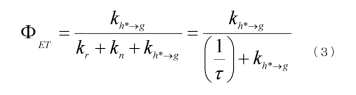
먼저, 수학식 3으로부터 에너지 이동 효율 ΦET를 높게 하기 위해서는, 에너지 이동의 속도 상수 kh*→g를 다른 경합하는 속도 상수 kr+kn(= 1/)에 비해 훨씬 크게 하면 좋은 것을 알 수 있다. 그리고, 그 에너지 이동의 속도 상수 kh*→g를 크게 하기 위해서는, 수학식 1 및 수학식 2로부터, 펠스터 기구, 덱스터 기구 중 어느 기구에서도, 호스트 분자의 발광 스펙트럼(일중항 여기 상태로부터의 에너지 이동을 논하는 경우는 형광 스펙트럼, 삼중항 여기 상태로부터의 에너지 이동을 논하는 경우는 인광 스펙트럼)과 게스트 분자의 흡수 스펙트럼과의 중첩이 큰 것이 좋은 것을 알 수 있다.First, in order to increase the energy transfer efficiency Φ ET from Equation (3), it can be seen that the energy transfer rate constant k h * → g should be made much larger than the other competitive rate constant k r + k n (= 1 / have. From equations (1) and (2), in order to increase the rate constant k h * - g of the energy transfer, the luminescence spectrum of the host molecule (from the singlet excited state The fluorescence spectrum when discussing energy transfer and the phosphorescence spectrum when discussing the energy transfer from triplet excited state) and the absorption spectrum of the guest molecule are preferably large.
여기서, 호스트 분자의 발광 스펙트럼과 게스트 분자의 흡수 스펙트럼과의 중첩을 고려함에 있어서, 게스트 분자의 흡수 스펙트럼에서의 가장 장파장(저에너지)측의 흡수대가 중요하다.Here, in consideration of overlapping between the emission spectrum of the host molecule and the absorption spectrum of the guest molecule, the absorption band on the side of the longest wavelength (low energy) in the absorption spectrum of the guest molecule is important.
본 실시형태에서는, 게스트 재료로서 인광성 화합물을 이용한다. 인광성 화합물의 흡수 스펙트럼에서, 발광에 가장 강하게 기여한다고 생각되는 흡수대는 기저 상태로부터 삼중항 여기 상태로의 직접 천이에 상당하는 흡수 파장 근방에 있고, 그것은 가장 장파장측에 나타나는 흡수대이다. 따라서, 호스트 재료의 발광 스펙트럼(형광 스펙트럼 및 인광 스펙트럼)은 인광성 화합물의 흡수 스펙트럼의 가장 장파장측의 흡수대와 중첩되는 것이 바람직하다고 생각된다.In the present embodiment, a phosphorescent compound is used as a guest material. In the absorption spectrum of the phosphorescent compound, the absorption band considered to contribute most strongly to luminescence is near the absorption wavelength corresponding to a direct transition from the ground state to the triplet excited state, and it is the absorption band appearing on the longest wavelength side. Therefore, it is considered that the luminescence spectrum (fluorescence spectrum and phosphorescence spectrum) of the host material is preferably overlapped with the absorption band on the longest wavelength side of the absorption spectrum of the phosphorescent compound.
예를 들면, 유기 금속 착체, 특히 발광성의 이리듐 착체에서, 가장 장파장측의 흡수대로서 500 nm 부근으로부터 600 nm 부근에 넓은 흡수대가 나타나는 경우가 많다. 이 흡수대는 주로 삼중항 MLCT(Metal to Ligand Charge Transfer) 천이에 유래한다. 단, 이 흡수대에는 삼중항 π-π* 천이나 일중항 MLCT 천이에 유래하는 흡수도 일부 포함되고, 이것들이 중첩하여, 흡수 스펙트럼의 가장 장파장측에 넓은 흡수대를 형성하고 있다고 생각된다. 따라서, 게스트 재료에 유기 금속 착체(특히 이리듐 착체)를 이용할 때는, 이와 같이 가장 장파장측에 존재하는 넓은 흡수대와 호스트 재료의 발광 스펙트럼이 크게 중첩되는 상태가 바람직하다.For example, in an organometallic complex, particularly a luminescent iridium complex, there is often a large absorption band near 500 nm to 600 nm as the absorption band on the longest wavelength side. This absorption band mainly comes from the triple-MLCT (Metal to Ligand Charge Transfer) transition. However, it is considered that this absorption band includes a part of the absorption attributable to triplet π-π * cloth or singlet MLCT transition and overlaps them to form a broad absorption band on the longest wavelength side of the absorption spectrum. Therefore, when an organometallic complex (especially an iridium complex) is used for the guest material, a state in which the luminescence spectrum of the host material and the broad absorption band on the longest wavelength side are greatly overlapped is preferable.
여기서 먼저, 호스트 재료의 삼중항 여기 상태로부터의 에너지 이동을 살펴보기로 한다. 상술한 논의로부터, 삼중항 여기 상태로부터의 에너지 이동에서는, 호스트 재료의 인광 스펙트럼과 게스트 재료의 가장 장파장측의 흡수대와의 중첩이 커지면 좋다.First, the energy transfer from the triplet excited state of the host material will be examined. From the above discussion, it is sufficient that the overlap between the phosphorescence spectrum of the host material and the absorption band on the longest wavelength side of the guest material becomes large in the energy transfer from the triplet excited state.
그러나, 이때 문제가 되는 것은, 호스트 분자의 일중항 여기 상태로부터의 에너지 이동이다. 삼중항 여기 상태로부터의 에너지 이동에 더하여, 일중항 여기 상태로부터의 에너지 이동도 효율적으로 행하려고 하면, 상술한 논의로부터, 호스트 재료의 인광 스펙트럼뿐만 아니라, 형광 스펙트럼도 게스트 재료의 가장 장파장측의 흡수대와 중첩하도록 설계해야 한다. 바꿔 말하면, 호스트 재료의 형광 스펙트럼이 인광 스펙트럼과 같은 위치에 오도록 호스트 재료를 설계하지 않으면, 호스트 재료의 일중항 여기 상태 및 삼중항 여기 상태의 쌍방으로부터의 에너지 이동을 효율적으로 행할 수는 없게 된다.However, what is problematic here is the energy transfer from the singlet excited state of the host molecule. In addition to the energy transfer from the triplet excited state, if the energy transfer from the singlet excited state is to be efficiently performed, not only the phosphorescence spectrum of the host material but also the fluorescence spectrum of the guest material, Should be designed to overlap. In other words, unless the host material is designed such that the fluorescence spectrum of the host material is in the same position as the phosphorescence spectrum, energy transfer from both the singlet excited state and the triplet excited state of the host material can not be performed efficiently.
그런데, 일반적으로, S1 준위와 T1 준위는 크게 다르기(S1 준위>T1 준위) 때문에, 형광의 발광 파장과 인광의 발광 파장도 크게 다르다(형광의 발광 파장<인광의 발광 파장). 예를 들면, 인광성 화합물을 이용한 발광 소자에서 종종 이용되는 4,4'-다이(N-카바졸일)바이페닐(약칭:CBP)은 500 nm 부근에 인광 스펙트럼을 갖지만, 한편으로 형광 스펙트럼은 400 nm 부근이며, 100 nm의 차이가 있다. 이 예로 생각해 보더라도, 호스트 재료의 형광 스펙트럼이 인광 스펙트럼과 같은 위치에 오도록 호스트 재료를 설계하는 것은 매우 어렵다.In general, since the S 1 and T 1 levels are significantly different (S 1 level> T 1 level), the emission wavelength of fluorescence differs greatly from that of phosphorescence (emission wavelength of fluorescence <emission wavelength of phosphorescence). For example, 4,4'-di (N-carbazolyl) biphenyl (abbreviation: CBP), which is often used in a light emitting device using a phosphorescent compound, has a phosphorescence spectrum near 500 nm, nm, with a difference of 100 nm. Considering this example, it is very difficult to design the host material such that the fluorescence spectrum of the host material is in the same position as the phosphorescence spectrum.
또한, 형광 발광은 인광 발광보다 높은 에너지 준위로부터의 발광이기 때문에, 형광 스펙트럼이 게스트 재료의 가장 장파장측의 흡수 스펙트럼에 근접하는 파장에 있는 호스트 재료의 T1 준위는 게스트 재료의 T1 준위를 밑돌게 된다.Further, the fluorescent light emission because light emitted from the higher energy level than the phosphorescent emission, T 1 level of the host material at the wavelength at which the fluorescence spectrum is close to the absorption spectrum of the long wavelength side of the guest material is lower than the T 1 level of the guest material .
따라서, 인광 발광 물질을 발광 중심 물질로 이용하는 경우, 발광층에 호스트 재료, 발광 중심 물질 외에 제3 물질을 포함하고, 호스트 재료 및 제3 물질은 여기 착체(들뜬 복합체(exciplex)라고도 함)를 형성하는 조합인 것이 바람직하다.Therefore, when a phosphorescent material is used as a luminescent center material, the host material and the third material include a host material and a luminescent center material in addition to the luminescent center material, and the host material and the third material form an excited complex (also called exciplex) Combination.
이 경우, 발광층에서의 캐리어(전자 및 정공)의 재결합 시에 호스트 재료와 제3 물질은 여기 착체를 형성한다. 여기 착체의 형광 스펙트럼은 호스트 재료 단체(單體), 및 제3 물질 단체의 형광 스펙트럼보다 장파장측에 스펙트럼을 갖는 발광이 되기 때문에, 호스트 재료 및 제3 물질의 T1 준위를 게스트 재료의 T1 준위보다 높게 유지한 채로, 일중항 여기 상태로부터의 에너지 이동을 최대한으로 높일 수 있다. 또한, 여기 착체는 T1 준위와 S1 준위가 근접하고 있는 상태이기 때문에, 형광 스펙트럼과 인광 스펙트럼이 거의 같은 위치에 존재한다. 따라서, 게스트 분자의 일중항 기저 상태로부터 삼중항 여기 상태에의 천이에 상당하는 흡수(게스트 분자의 흡수 스펙트럼에서의 가장 장파장측에 존재하는 넓은 흡수대)에 여기 착체의 형광 스펙트럼 및 인광 스펙트럼의 양쪽 모두를 크게 중첩하는 것이 가능하게 되기 때문에, 에너지 이동 효율이 높은 발광 소자를 얻을 수 있다.In this case, upon recombination of the carriers (electrons and holes) in the light-emitting layer, the host material and the third material form excited complexes. Since the fluorescence spectrum of the excited complex is luminescence having a spectrum on the longer wavelength side than the host material alone and the fluorescence spectrum of the third substance alone, the T 1 level of the host material and the third substance is set to T 1 The energy transfer from the singly excited state can be maximized while the voltage is kept higher than the energy level. Further, since the excited complex has a state in which the T 1 and S 1 levels are close to each other, the fluorescence spectrum and the phosphorescence spectrum exist at substantially the same positions. Therefore, both of the fluorescence spectrum and the phosphorescence spectrum of the excitation complex in the absorption corresponding to the transition from the singlet ground state to the triplet excited state of the guest molecule (a wide absorption band on the longest wavelength side in the absorption spectrum of the guest molecule) It is possible to obtain a light emitting device having a high energy transfer efficiency.
제3 물질로서는, 상기 호스트 재료나 첨가물로서 이용할 수 있는 재료로서 예로 든 재료를 이용할 수 있다. 또한, 호스트 재료 및 제3 물질은 여기 착체를 일으키는 조합이면 좋지만, 전자를 받기 쉬운 화합물(전자 수송성을 갖는 화합물)과 정공을 받기 쉬운 화합물(정공 수송성을 갖는 화합물)을 조합하는 것이 바람직하다.As the third material, materials exemplified as materials usable as the host material and the additive can be used. The host material and the third material may be a combination that causes an excited complex, but it is preferable to combine a compound that is easily electron-sensitive (a compound having electron-transporting property) and a compound that is susceptible to hole (a compound having hole-transporting property).
전자 수송성을 갖는 화합물과 정공 수송성을 갖는 화합물로 호스트 재료와 제3 물질을 구성하는 경우, 그 혼합비에 의해 캐리어 밸런스를 제어할 수도 있다. 구체적으로는, 호스트 재료:제3 물질(또는 첨가물) = 1:9 내지 9:1의 범위가 바람직하다. 또한, 이 때, 일 종류의 발광 중심 물질이 분산된 발광층을 2층으로 분할하고, 호스트 재료와 제3 물질의 혼합 비율을 다르게 하는 구성으로 해도 좋다. 이것에 의해, 발광 소자의 캐리어 밸런스를 최적화할 수 있어, 수명을 향상시키는 것이 가능하게 된다. 또한, 한쪽의 발광층을 정공 수송성의 층으로 하고, 다른 한쪽의 발광층을 전자 수송성의 층으로 해도 좋다.When a host material and a third material are constituted of a compound having electron transporting property and a compound having hole transporting property, the carrier balance can be controlled by the mixing ratio. Concretely, the range of the host material: the third material (or the additive) = 1: 9 to 9: 1 is preferable. In this case, the light emitting layer in which one type of luminescent center material is dispersed may be divided into two layers, and the mixing ratio of the host material and the third material may be different. As a result, it is possible to optimize the carrier balance of the light emitting element and to improve the lifetime. Further, one of the light-emitting layers may be a hole-transporting layer and the other light-emitting layer may be an electron-transporting layer.
이상과 같은 구성을 갖는 발광층은 복수의 재료로 구성되어 있는 경우, 진공 증착법에서의 공증착이나, 혼합 용액으로서 잉크젯법이나 스핀 코트법이나 딥 코트법 등을 이용하여 제작할 수 있다.When the light-emitting layer having the above-described structure is composed of a plurality of materials, it can be produced by co-evaporation in vacuum deposition or by ink-jet, spin-coating, dip coating or the like as a mixed solution.
전자 수송층(114)은 전자 수송성을 갖는 물질을 포함하는 층이다. 예를 들면, 트리스(8-퀴놀리놀라토)알루미늄(약칭:Alq), 트리스(4-메틸-8-퀴놀리놀라토)알루미늄(약칭:Almq3), 비스(10-하이드록시다이벤조[h]퀴놀리나토)베릴륨(약칭:BeBq2), 비스(2-메틸-8-퀴놀리놀라토)(4-페닐페놀라토)알루미늄(약칭:BAlq) 등, 퀴놀린 골격 또는 벤조퀴놀린 골격을 갖는 금속 착체 등으로 이루어지는 층이다. 또한, 이 외에, 비스[2-(2-하이드록시페닐)벤즈옥사졸라토]아연(약칭:Zn(BOX)2), 비스[2-(2-하이드록시페닐)벤조티아졸라토]아연(약칭:Zn(BTZ)2) 등의 옥사졸계, 티아졸계 배위자를 갖는 금속 착체 등도 이용할 수 있다. 또한, 금속 착체 이외에도, 2-(4-바이페닐일)-5-(4-tert-부틸페닐)-1,3,4-옥사다이아졸(약칭:PBD)이나, 1,3-비스[5-(p-tert-부틸페닐)-1,3,4-옥사다이아졸-2-일]벤젠(약칭:OXD-7), 3-(4-바이페닐일)-4-페닐-5-(4-tert-부틸페닐)-1,2,4-트리아졸(약칭:TAZ), 바소페난트롤린(약칭:BPhen), 바소큐프로인(약칭:BCP) 등도 이용할 수 있다. 여기에 설명한 물질은 주로 10-6 cm2/Vs 이상의 전자 이동도를 갖는 물질이다. 또한, 정공보다 전자의 수송성이 높은 물질이면, 상기 이외의 물질을 전자 수송층으로서 이용해도 상관없다.The electron transporting layer 114 is a layer containing a substance having an electron transporting property. (Abbreviation: Alq), tris (4-methyl-8-quinolinolato) aluminum (abbreviation: Almq 3 ), bis (10-hydroxydibenzo [ quinolinato) beryllium (abbreviated as BeBq 2 ), aluminum (abbreviation: BAlq), bis (2-methyl-8-quinolinolato) Metal complexes and the like. Further, in addition to the above compounds, there may be mentioned bis (2- (2-hydroxyphenyl) benzoxazolato] zinc (abbreviated as Zn (BOX) 2 ), bis [2- (2-hydroxyphenyl) benzothiazolato] An abbreviation: Zn (BTZ) 2 ), and a metal complex having a thiazole ligand can also be used. Further, in addition to the metal complexes, there may be mentioned 2- (4-biphenylyl) -5- (4- tert -butylphenyl) -1,3,4-oxadiazole (abbreviation: PBD) - (p- tert -butylphenyl) -1,3,4-oxadiazol-2-yl] benzene (abbreviation: OXD- 4- tert -butylphenyl) -1,2,4-triazole (abbreviated as TAZ), basophenanthroline (abbreviated as BPhen), and basocuproin (abbreviation: BCP). The materials described here are mainly those having an electron mobility of 10 -6 cm 2 / Vs or more. Further, in the case of a substance having higher electron transportability than holes, a substance other than the above may be used as an electron transporting layer.
또한, 벤조티에노피리미딘 골격을 갖는 화합물을 전자 수송층(114)을 구성하는 재료로서 이용해도 좋다. 벤조티에노피리미딘 골격을 갖는 화합물은 밴드 갭이 넓고, 삼중항 여기 준위(T1 준위)가 높은 물질이기 때문에, 발광층에서의 여기 에너지가 전자 수송층(114)으로 이동하는 것을 효과적으로 방지하고, 그것을 원인으로 하는 발광 효율의 저하를 억제하여, 발광 효율이 높은 발광 소자를 얻는 것이 가능하게 된다. 또한, 벤조티에노피리미딘 골격을 갖는 화합물은 캐리어 수송성이 우수하기 때문에, 구동 전압이 낮은 발광 소자를 제공하는 것이 가능하게 된다.Further, a compound having a benzothienopyrimidine skeleton may be used as a material constituting the electron transport layer 114. Since the compound having a benzothienopyrimidine skeleton has a wide band gap and a high triplet excitation level (T 1 level), it is possible to effectively prevent the excitation energy in the light emitting layer from moving to the electron transport layer 114, It is possible to suppress the lowering of the light emitting efficiency and cause the light emitting element to have a high light emitting efficiency. In addition, since the compound having a benzothienopyrimidine skeleton has excellent carrier transportability, it becomes possible to provide a light emitting device having a low driving voltage.
또한, 전자 수송층은 단층의 것뿐만 아니라, 상기 물질로 이루어지는 층이 2층 이상 적층된 것으로 해도 좋다.Further, the electron transporting layer may be formed not only of a single layer but also a layer of two or more layers made of the above-described material.
또한, 전자 수송층과 발광층과의 사이에 전자 캐리어의 이동을 제어하는 층을 제공해도 좋다. 이것은 상술한 바와 같은 전자 수송성이 높은 재료에 전자 트랩성이 높은 물질을 소량 첨가한 층이며, 전자 캐리어의 이동을 억제함으로써, 캐리어 밸런스를 조절하는 것이 가능하게 된다. 이러한 구성은 발광층을 전자가 관통함으로써 발생하는 문제(예를 들면 소자 수명의 저하)의 억제에 큰 효과를 발휘한다.Further, a layer for controlling the movement of the electron carrier may be provided between the electron transporting layer and the light emitting layer. This is a layer in which a small amount of a substance having a high electron trapping property is added to a material having a high electron transportability as described above, and it is possible to control the carrier balance by suppressing the movement of the electron carrier. This configuration exerts a great effect for suppressing problems (for example, deterioration of device life) caused by electrons passing through the light-emitting layer.
또한, 발광층의 호스트 재료와 전자 수송층을 구성하는 재료에는 공통되는 골격이 존재하는 것이 바람직하다. 이것에 의해, 캐리어의 이동이 보다 순조롭게 되어, 구동 전압의 저감시킬 수 있다. 또한, 상기 호스트 재료와 전자 수송층을 구성하는 재료를 같은 물질로 구성하면 효과가 높다.Further, it is preferable that a skeleton common to the host material of the light emitting layer and the material constituting the electron transporting layer exists. As a result, the movement of the carrier becomes smoother, and the driving voltage can be reduced. In addition, the effect is high when the materials constituting the host material and the electron transport layer are made of the same material.
또한, 전자 수송층(114)과 제2 전극(102)과의 사이에, 제2 전극(102)에 접하여 전자 주입층(115)을 제공해도 좋다. 전자 주입층(115)으로서는, 리튬, 칼슘, 불화 리튬(LiF), 불화 세슘(CsF), 불화 칼슘(CaF2) 등을 이용할 수 있다. 또한, 전자 수송성을 갖는 물질과 상기 물질에 대한 전자 공여성을 갖는 물질(이하 간단히 전자 공여성 물질이라고 칭함)과의 복합 재료를 이용할 수도 있다. 전자 공여성 물질로서는, 알칼리 금속 또는 알칼리 토금속 또는 그들의 화합물을 들 수 있다. 또한, 전자 주입층(115)으로서 이러한 복합 재료를 이용함으로써, 제2 전극(102)으로부터의 전자 주입이 효율적으로 행해지기 때문에, 보다 바람직한 구성이 된다. 이 구성으로 함으로써, 음극으로서 일 함수가 작은 재료뿐만 아니라, 그 외의 도전 재료를 이용하는 것도 가능하게 된다.The
음극으로서 기능하는 전극을 형성하는 물질로서는, 일 함수가 작은(구체적으로는 3.8 eV 이하) 금속, 합금, 전기 전도성 화합물, 및 이들의 혼합물 등을 이용할 수 있다. 이러한 음극 재료의 구체적인 예로서는, 원소 주기표의 제1 족 또는 제2 족에 속하는 원소, 즉 리튬(Li)이나 세슘(Cs), 마그네슘(Mg), 칼슘(Ca), 스트론튬(Sr) 등 및 이것들을 포함하는 합금(MgAg, AlLi)이나 유로퓸(Eu), 이테르븀(Yb) 등의 희토류 금속 및 이것들을 포함하는 합금 등을 들 수 있다. 그러나, 제2 전극(102)과 전자 수송층과의 사이에, 전자 주입층을 형성함으로써, 일 함수의 대소에 상관없이, Al, Ag, ITO, 규소, 혹은 산화 규소를 함유한 인듐 주석 산화물 등 다양한 도전성 재료를 제2 전극(102)으로서 이용할 수 있다. 이들 도전성 재료는 스퍼터링법이나 잉크젯법, 스핀 코트법 등을 이용하여 성막하는 것이 가능하다.As the material for forming the electrode functioning as the cathode, a metal having a small work function (specifically, 3.8 eV or less), an alloy, an electrically conductive compound, a mixture thereof and the like can be used. Specific examples of such an anode material include lithium (Li), cesium (Cs), magnesium (Mg), calcium (Ca), strontium (Sr) and the like belonging to the first group or the second group of the element periodic table, (MgAg, AlLi), rare earth metals such as europium (Eu) and ytterbium (Yb), and alloys containing them. However, by forming the electron injecting layer between the
또한, EL층(103)의 형성 방법으로서는, 건식법, 습식법을 불문하고, 다양한 방법을 이용할 수 있다. 예를 들면, 진공 증착법, 잉크젯법, 또는 스핀 코트법 등을 이용해도 상관없다. 또한 각 전극 또는 각 층마다 다른 성막 방법을 이용하여 형성해도 상관없다.As the method of forming the
전극에 대해서도, 졸-겔법이나, 금속 재료의 페이스트를 이용하여 습식법으로 형성해도 좋다. 또한, 스퍼터링법이나 진공 증착법 등의 건식법을 이용하여 형성해도 좋다.The electrode may also be formed by a wet process using a sol-gel method or a paste of a metal material. It may also be formed by a dry method such as a sputtering method or a vacuum evaporation method.
또한, 제1 전극(101)과 제2 전극(102) 사이에 제공되는 EL층의 구성은 상기의 것에 한정되는 것은 아니다. 그러나, 발광 영역과 전극이나 캐리어 주입층에 이용되는 금속이 근접하는 것에 의해 생기는 소광이 억제되도록, 제1 전극(101) 및 제2 전극(102)으로부터 떨어진 부위에 정공과 전자가 재결합하는 발광 영역을 형성하는 구성이 바람직하다.The structure of the EL layer provided between the
또한, 직접 발광층에 접하는 정공 수송층이나 전자 수송층, 특히 발광층(113)에서의 발광 영역에 가까운 쪽에 접하는 캐리어 수송층은 발광층에서 생성한 여기자로부터의 에너지 이동을 억제하기 위해, 그 에너지 갭이 발광층을 구성하는 발광 물질 혹은, 발광층에 포함되는 발광 중심 물질이 갖는 에너지 갭보다 큰 에너지 갭을 갖는 물질로 구성하는 것이 바람직하다.In order to suppress energy transfer from the excitons generated in the light emitting layer, a hole transporting layer or an electron transporting layer in contact with the direct light emitting layer, particularly, a carrier transporting layer in contact with the
이상과 같은 구성을 갖는 발광 소자는 제1 전극(101)과 제2 전극(102)과의 사이에 생긴 전위차에 의해 전류가 흘러, 발광성이 높은 물질을 포함하는 층인 발광층(113)에서 정공과 전자가 재결합하여, 발광하는 것이다. 즉 발광층(113)에 발광 영역이 형성되는 구성으로 되어 있다.In the light emitting device having the above-described configuration, a current flows due to a potential difference generated between the
발광은 제1 전극(101) 또는 제2 전극(102) 중 어느 한쪽 또는 양쪽 모두를 통하여 외부로 취출된다. 따라서, 제1 전극(101) 또는 제2 전극(102) 중 어느 한쪽 또는 양쪽 모두는 투광성을 갖는 전극으로 이루어진다. 제1 전극(101)만이 투광성을 갖는 전극인 경우, 발광은 제1 전극(101)을 통하여 기판측으로부터 취출된다. 또한, 제2 전극(102)만이 투광성을 갖는 전극인 경우, 발광은 제2 전극(102)을 통하여 기판과 반대쪽에서 취출된다. 제1 전극(101) 및 제2 전극(102)이 모두 투광성을 갖는 전극인 경우, 발광은 제1 전극(101) 및 제2 전극(102)을 통하여, 기판측 및 기판과 반대쪽의 양쪽 모두로부터 취출된다.Light emission is extracted to the outside through either or both of the
본 실시형태에서의 발광 소자는 에너지 갭이 큰 벤조티에노피리미딘 골격을 갖는 화합물이 이용되고 있기 때문에, 발광 중심 물질이 에너지 갭이 큰 청색의 형광을 나타내는 물질이나 녹색 내지 청색의 인광을 발하는 물질이어도, 효율적으로 발광시킬 수 있어, 발광 효율이 양호한 발광 소자를 얻을 수 있게 된다. 이로 인하여, 보다 저소비 전력의 발광 소자를 제공하는 것이 가능하게 된다. 또한, 벤조티에노피리미딘 골격을 갖는 화합물은 캐리어의 수송성이 우수하기 때문에, 구동 전압이 낮은 발광 소자를 제공하는 것이 가능하게 된다.Since the compound having a benzothienopyrimidine skeleton having a large energy gap is used as the light emitting element in the present embodiment, the luminescent center substance is a substance showing blue fluorescence having a large energy gap or a substance emitting blue or green phosphorescence It is possible to efficiently emit light and to obtain a light emitting element having a good light emitting efficiency. This makes it possible to provide a light emitting device with a lower power consumption. In addition, since the compound having a benzothienopyrimidine skeleton has excellent carrier transportability, it becomes possible to provide a light emitting device having a low driving voltage.
이러한 발광 소자는 유리, 플라스틱 등으로 이루어지는 기판을 지지체로서 제작하면 좋다. 일 기판 위에 이러한 발광 소자를 복수 제작함으로써, 패시브 매트릭스형의 발광 장치를 제작할 수 있다. 또한, 유리, 플라스틱 등으로 이루어지는 기판 위에, 트랜지스터를 형성하고, 트랜지스터와 전기적으로 접속된 전극 위에 상기 발광 소자를 제작해도 좋다. 이것에 의해, 트랜지스터에 의해 발광 소자의 구동을 제어하는 액티브 매트릭스형의 발광 장치를 제작할 수 있다. 또한, 트랜지스터의 구조는 특별히 한정되지 않는다. 스태거형의 TFT여도 좋고 역스태거형의 TFT여도 좋다. 또한, TFT에 이용하는 반도체의 결정성에 대해서도 특별히 한정되지 않는다. 또한, TFT 기판에 형성되는 구동용 회로에 대해서도, N형 및 P형의 TFT로 이루어지는 것이어도 좋고, 혹은 N형의 TFT 또는 P형의 TFT 중 어느 한쪽으로만 이루어지는 것이어도 좋다. TFT를 구성하는 반도체층의 재료로서는 실리콘(Si) 및 게르마늄(Ge) 등의 원소 주기표의 제14 족 원소, 갈륨 비소 및 인듐 인 등의 화합물, 및 산화 아연 및 산화 주석 등의 산화물 등 반도체 특성을 나타내는 물질이면 어떠한 재료를 이용해도 좋다. 반도체 특성을 나타내는 산화물(산화물 반도체)로서는, 인듐, 갈륨, 알루미늄, 아연, 및 주석으로부터 선택한 원소의 복합 산화물을 이용할 수 있다. 예를 들면, 산화 아연(ZnO), 산화 아연을 포함하는 산화 인듐(Indium Zinc Oxide), 및 산화 인듐, 산화 갈륨, 및 산화 아연으로 이루어지는 산화물(IGZO:Indium Gallium Zinc Oxide)을 그 예로 들 수 있다. 또한, 유기 반도체를 이용해도 좋다. 상기 반도체층은 결정질 구조, 비정질 구조 중 어느 구조여도 좋다. 또한, 결정질 구조의 반도체층의 구체적인 예로서는, 단결정 반도체, 다결정 반도체, 혹은 미결정 반도체를 들 수 있다.Such a light-emitting element may be produced by using a substrate made of glass, plastic or the like as a support. By manufacturing a plurality of such light emitting elements on one substrate, a passive matrix type light emitting device can be manufactured. Alternatively, a transistor may be formed on a substrate made of glass, plastic, or the like, and the above-described light emitting device may be fabricated on an electrode electrically connected to the transistor. Thus, an active matrix type light emitting device that controls the driving of the light emitting element by the transistor can be manufactured. The structure of the transistor is not particularly limited. It may be a stagger type TFT or a reverse stagger type TFT. The crystallinity of the semiconductor used for the TFT is not particularly limited either. Further, the driving circuit formed on the TFT substrate may be composed of N-type or P-type TFTs, or may be composed of only one of N-type TFTs or P-type TFTs. Examples of the material of the semiconductor layer constituting the TFT include semiconductor materials such as silicon (Si) and germanium (Ge), such as Group 14 elements in the periodic table, compounds such as gallium arsenide and indium phosphorus, and oxides such as zinc oxide and tin oxide Any material may be used. As the oxide (oxide semiconductor) exhibiting semiconductor characteristics, a complex oxide of an element selected from indium, gallium, aluminum, zinc, and tin can be used. Examples thereof include indium zinc oxide (ZnO), indium oxide containing zinc oxide, and indium gallium zinc oxide (IGZO), which are indium oxide, gallium oxide, and zinc oxide . An organic semiconductor may also be used. The semiconductor layer may have any of a crystalline structure and an amorphous structure. Specific examples of the semiconductor layer having a crystalline structure include a single crystal semiconductor, a polycrystalline semiconductor, and a microcrystalline semiconductor.
(실시형태 3)(Embodiment 3)
본 실시형태는 복수의 발광 유닛을 적층한 구성의 발광 소자(이하, 적층형 소자라고도 함)의 양태에 대하여, 도 1의 (B)을 참조하여 설명한다. 이 발광 소자는 제1 전극과 제2 전극과의 사이에, 복수의 발광 유닛을 갖는 발광 소자이다. 하나의 발광 유닛은 실시형태 2에 나타낸 EL층(103)과 같은 구성을 가진다. 즉, 실시형태 2에 나타낸 발광 소자는 하나의 발광 유닛을 갖는 발광 소자이며, 본 실시형태에서는 복수의 발광 유닛을 갖는 발광 소자라고 할 수 있다.The present embodiment will be described with reference to Fig. 1 (B) of a mode of a light emitting element having a structure in which a plurality of light emitting units are stacked (hereinafter also referred to as a stacked element). This light emitting element is a light emitting element having a plurality of light emitting units between the first electrode and the second electrode. One light emitting unit has the same configuration as the
도 1의 (B)에서, 제1 전극(501)과 제2 전극(502)과의 사이에는 제1 발광 유닛(511)과 제2 발광 유닛(512)이 적층되어 있고, 제1 발광 유닛(511)과 제2 발광 유닛(512)과의 사이에는 전하 발생층(513)이 제공되어 있다. 제1 전극(501)과 제2 전극(502)은 각각 실시형태 2에서의 제1 전극(101)과 제2 전극(102)에 상당하고, 실시형태 2에 설명한 것과 같은 것을 적용할 수 있다. 또한, 제1 발광 유닛(511)과 제2 발광 유닛(512)은 같은 구성이어도 다른 구성이어도 좋다.1B, a first
전하 발생층(513)에는 유기 화합물과 금속 산화물의 복합 재료가 포함되어 있다. 이 유기 화합물과 금속 산화물의 복합 재료는 실시형태 2에 나타낸 정공 주입층에 이용할 수 있는 복합 재료를 이용할 수 있다. 유기 화합물로서는 방향족 아민 화합물, 카바졸 화합물, 방향족 탄화 수소, 고분자 화합물(올리고머, 덴드리머, 폴리머 등) 등, 다양한 화합물을 이용할 수 있다. 또한, 유기 화합물로서는, 정공 이동도가 1×10⁻⁶ cm2/Vs 이상인 것을 적용하는 것이 바람직하다. 단, 전자보다 정공의 수송성이 높은 물질이면, 이것들 이외의 것을 이용해도 좋다. 유기 화합물과 금속 산화물의 복합 재료는 캐리어 주입성, 캐리어 수송성이 우수하기 때문에, 저전압 구동, 저전류 구동을 실현할 수 있다. 또한, 양극측의 계면이 전하 발생층에 접하고 있는 발광 유닛은 전하 발생층이 정공 수송층의 역할도 담당할 수 있기 때문에, 정공 수송층을 제공하지 않아도 좋다.The
또한, 전하 발생층(513)은 유기 화합물과 금속 산화물의 복합 재료를 포함하는 층과 다른 재료에 의해 구성되는 층을 조합한 적층 구조로 형성해도 좋다. 예를 들면, 유기 화합물과 금속 산화물의 복합 재료를 포함하는 층과, 전자 공여성 물질 중에서 선택된 하나의 화합물과 전자 수송성이 높은 화합물을 포함하는 층을 조합하여 형성해도 좋다. 또한, 유기 화합물과 금속 산화물의 복합 재료를 포함하는 층과 투명 도전막을 조합하여 형성해도 좋다.Further, the
어쨌든, 제1 발광 유닛(511)과 제2 발광 유닛(512)에 끼워지는 전하 발생층(513)은 제1 전극(501)과 제2 전극(502)에 전압을 인가했을 때에, 한쪽의 발광 유닛에 전자를 주입하고, 다른 한쪽의 발광 유닛에 정공을 주입하는 것이면 좋다. 예를 들면, 도 1의 (B)에서, 제1 전극의 전위가 제2 전극의 전위보다 높아지도록 전압을 인가한 경우, 전하 발생층(513)은 제1 발광 유닛(511)에 전자를 주입하고, 제2 발광 유닛(512)에 정공을 주입하는 것이면 좋다.In any case, when a voltage is applied to the
본 실시형태에서는, 2개의 발광 유닛을 갖는 발광 소자에 대하여 설명했지만, 3개 이상의 발광 유닛을 적층한 발광 소자에 대해서도, 마찬가지로 적용하는 것이 가능하다. 본 실시형태에 따른 발광 소자와 같이, 한쌍의 전극 사이에 복수의 발광 유닛을 전하 발생층에 의해 나누어 배치함으로써, 전류 밀도를 낮게 유지한 채, 고휘도 발광을 가능하게 하고, 더욱 장수명의 소자를 실현할 수 있다. 또한, 저전압 구동이 가능하고 소비 전력이 낮은 발광 장치를 실현할 수 있다.In the present embodiment, the light emitting element having two light emitting units has been described. However, the same can be applied to a light emitting element in which three or more light emitting units are stacked. As in the light emitting device according to the present embodiment, by disposing a plurality of light emitting units between a pair of electrodes by the charge generation layer, it is possible to realize high luminance light emission while maintaining a low current density, . Further, it is possible to realize a light emitting device capable of low voltage driving and having low power consumption.
또한, 각각의 발광 유닛의 발광색을 다르게 함으로써, 발광 소자 전체적으로 원하는 색의 발광을 얻을 수 있다. 예를 들면, 2개의 발광 유닛을 갖는 발광 소자에서 제1 발광 유닛의 발광색과 제2 발광 유닛의 발광색을 보색의 관계가 되도록 함으로써, 발광 소자 전체적으로 백색 발광하는 발광 소자를 얻는 것도 가능하다. 또한, 보색이란, 혼합하면 무채색이 되는 색들의 관계를 말한다. 즉, 보색의 관계에 있는 색을 발광하는 물질로부터 얻어진 광을 혼합하면, 백색 발광을 얻을 수 있다. 또한, 3개의 발광 유닛을 갖는 발광 소자의 경우에도 마찬가지이고, 예를 들면, 제1 발광 유닛의 발광색이 적색이고, 제2 발광 유닛의 발광색이 녹색이고, 제3 발광 유닛의 발광색이 청색인 경우, 발광 소자 전체적으로는, 백색 발광을 얻을 수 있다. 또한, 한쪽의 발광 유닛에서는 인광 발광을 나타내는 발광 중심 물질을 이용한 발광층을, 다른 한쪽의 발광 유닛에서는 형광 발광을 나타내는 발광 중심 물질을 이용한 발광층을 적용함으로써, 하나의 발광 소자에서 형광 발광, 인광 발광의 양쪽 모두를 효율적으로 발광시킬 수 있다. 예를 들면, 한쪽의 발광 유닛에서는 적색과 녹색의 인광 발광을 얻고, 다른 한쪽의 발광 유닛에서는 청색의 형광 발광을 얻음으로써, 발광 효율이 양호한 백색 발광을 얻을 수 있다.Further, by making the luminescent colors of the respective luminescent units different, luminescence of a desired color can be obtained as a whole of the luminescent elements. For example, in a light emitting element having two light emitting units, it is possible to obtain a light emitting element which emits white light as a whole by making the light emitting color of the first light emitting unit and the light emitting color of the second light emitting unit be complementary colors. In addition, complementary color refers to the relationship of colors that become achromatic when mixed. That is, when light obtained from a material emitting a color in the complementary color relationship is mixed, white light emission can be obtained. The same applies to the case of the light emitting element having three light emitting units. For example, when the light emitting color of the first light emitting unit is red, the light emitting color of the second light emitting unit is green, and the light emitting color of the third light emitting unit is blue , White light emission can be obtained as a whole of the light emitting element. Further, by applying a light emitting layer using a luminescent center material that exhibits phosphorescence luminescence in one light emitting unit and a luminescent layer using a luminescent center material that exhibits fluorescence luminescence in the other light emitting unit, It is possible to efficiently emit both of them. For example, white light emission with good light emission efficiency can be obtained by obtaining phosphorescence emission of red and green in one light emission unit and blue fluorescence emission in the other light emission unit.
본 실시형태의 발광 소자는 벤조티에노피리미딘 골격을 갖는 화합물을 포함하기 때문에, 발광 효율이 양호한 발광 소자로 할 수 있다. 또한, 구동 전압이 낮은 발광 소자로 할 수 있다. 또한, 상기 헤테로환 화합물이 포함되는 발광 유닛은 발광 중심 물질 유래의 광을 색순도 좋게 얻을 수 있기 때문에, 발광 소자 전체적으로의 색의 조제가 용이해진다.Since the light emitting element of the present embodiment includes a compound having a benzothienopyrimidine skeleton, a light emitting element having good light emitting efficiency can be obtained. Further, a light emitting element having a low driving voltage can be obtained. Further, since the light-emitting unit including the heterocyclic compound can obtain light from the light-emitting center material in a color-purity degree, it is easy to prepare the whole color of the light-emitting element.
또한, 본 실시형태는 다른 실시형태와 적절히 조합하는 것이 가능하다.The present embodiment can be combined with other embodiments as appropriate.
(실시형태 4)(Fourth Embodiment)
본 실시형태에서는 벤조티에노피리미딘 골격을 갖는 화합물을 포함하는 발광 소자를 이용한 발광 장치에 대하여 설명한다.In this embodiment, a light emitting device using a light emitting element including a compound having a benzothienopyrimidine skeleton will be described.
본 실시형태에서는, 벤조티에노피리미딘 골격을 갖는 화합물을 포함하는 발광 소자를 이용하여 제작된 발광 장치의 일례에 대하여 도 2를 이용하여 설명한다. 또한, 도 2의 (A)는 발광 장치를 나타내는 상면도, 도 2의 (B)는 도 2의 (A)를 A-B 및 C-D로 절단한 단면도이다. 이 발광 장치는 발광 소자의 발광을 제어하는 것으로서, 점선으로 나타낸 구동 회로부(소스측 구동 회로)(601), 화소부(602), 구동 회로부(게이트측 구동 회로)(603)를 포함한다. 또한, 부호 604는 밀봉 기판, 625는 건조재, 605는 실재이며, 실재(605)로 둘러싸인 내측은 공간(607)으로 되어 있다.In the present embodiment, an example of a light emitting device manufactured using a light emitting element including a compound having a benzothienopyrimidine skeleton will be described with reference to FIG. 2 (A) is a top view showing the light emitting device, and Fig. 2 (B) is a sectional view taken along line A-B and C-D in Fig. This light emitting device controls light emission of the light emitting element and includes a driving circuit portion (source side driving circuit) 601, a
또한, 리드 배선(608)은 소스측 구동 회로(601) 및 게이트측 구동 회로(603)에 입력되는 신호를 전송하기 위한 배선이며, 외부 입력 단자가 되는 FPC(Flexible Printed Circuit)(609)로부터 비디오 신호, 클록 신호, 스타트 신호, 리셋 신호 등을 받는다. 또한, 여기에서는 FPC밖에 도시하지 않았지만, 이 FPC에는 프린트 배선 기판(PWB)이 부착되어 있어도 좋다. 본 명세서에서의 발광 장치에는 발광 장치 본체뿐만 아니라, 거기에 FPC 혹은 PWB가 장착된 상태도 포함하는 것으로 한다.The lead wirings 608 are wirings for transmitting signals inputted to the source
다음에, 단면 구조에 대하여 도 2의 (B)를 이용하여 설명한다. 소자 기판(610) 위에는 구동 회로부 및 화소부가 형성되어 있지만, 여기에서는, 구동 회로부인 소스측 구동 회로(601)와 화소부(602) 내의 하나의 화소가 도시되어 있다.Next, the cross-sectional structure will be described with reference to Fig. 2 (B). A driver circuit portion and a pixel portion are formed on the
또한, 소스측 구동 회로(601)는 n채널형 TFT(623)와 p채널형 TFT(624)를 조합한 CMOS 회로가 형성된다. 또한, 구동 회로는 다양한 CMOS 회로, PMOS 회로, 혹은 NMOS 회로로 형성해도 좋다. 또한, 본 실시형태에서는, 기판 위에 구동 회로를 형성한 드라이버 일체형을 나타내지만, 반드시 그럴 필요는 없고, 구동 회로를 기판 위가 아니라 외부에 형성할 수도 있다.In the source
또한, 화소부(602)는 스위칭용 TFT(611)와, 전류 제어용 TFT(612)와, 전류 제어용 TFT(612)의 드레인에 전기적으로 접속된 제1 전극(613)을 포함하는 복수의 화소에 의해 형성된다. 또한, 제1 전극(613)의 단부를 덮어 절연물(614)이 형성되어 있다. 여기에서는 포지티브형의 감광성 수지막을 이용함으로써 형성할 수 있다.The
또한, 위에 형성되는 막의 커버리지(coverage)를 양호한 것으로 하기 위해, 절연물(614)의 상단부 또는 하단부에 곡률을 갖는 면이 형성되도록 한다. 예를 들면, 절연물(614)의 재료로서 포지티브형의 감광성 아크릴을 이용한 경우, 절연물(614)의 상단부에만 곡률 반경(0.2μm 이상 3μm 이하)을 갖는 곡면을 갖게 하는 것이 바람직하다. 또한, 절연물(614)로서 네거티브형의 감광 재료, 혹은 포지티브형의 감광 재료를 모두 사용할 수 있다.Further, in order to make the coverage of the film formed on the upper surface better, a curved surface is formed at the upper end or the lower end of the insulating
제1 전극(613) 위에는, EL층(616), 및 제2 전극(617)이 각각 형성되어 있다. 여기서, 양극으로서 기능하는 제1 전극(613)에 이용하는 재료로서는, 일 함수가 큰 재료를 이용하는 것이 바람직하다. 예를 들면, ITO막, 또는 규소를 함유한 인듐 주석 산화물막, 2 wt% 이상 20 wt% 이하의 산화 아연을 포함하는 산화 인듐막, 질화 티탄막, 크롬막, 텅스텐막, Zn막, Pt막 등의 단층막 외에, 질화 티탄과 알루미늄을 주성분으로 하는 막과의 적층, 질화 티탄막과 알루미늄을 주성분으로 하는 막과 질화 티탄막과의 3층 구조 등을 이용할 수 있다. 또한, 적층 구조로 하면, 배선으로서의 저항도 낮고, 양호한 오믹 콘택트를 취할 수 있어, 또한 양극으로서 기능시킬 수 있다.An
또한, EL층(616)은 증착 마스크를 이용한 증착법, 잉크젯법, 스핀 코트법 등의 다양한 방법에 의해 형성된다. EL층(616)은 벤조티에노피리미딘 골격을 갖는 화합물을 포함하고 있다. 또한, EL층(616)을 구성하는 다른 재료로서는, 저분자 화합물, 또는 고분자 화합물(올리고머, 덴드리머를 포함함)이어도 좋다.The
또한, EL층(616) 위에 형성되어 음극으로서 기능하는 제2 전극(617)에 이용하는 재료로서는, 일 함수가 작은 재료(Al, Mg, Li, Ca, 또는 이러한 합금이나 화합물, MgAg, MgIn, AlLi 등)를 이용하는 것이 바람직하다. 또한, EL층(616)에서 생긴 광이 제2 전극(617)을 투과시키는 경우에는, 제2 전극(617)으로서 막 두께를 얇게 한 금속 박막과 투명 도전막(ITO, 2∼20 wt%의 산화 아연을 포함하는 산화 인듐, 규소를 함유한 인듐 주석 산화물, 산화 아연(ZnO) 등)과의 적층을 이용하는 것이 좋다.The material used for the second electrode 617 formed on the
또한, 제1 전극(613), EL층(616), 제2 전극(617)으로, 발광 소자가 형성된다. 상기 발광 소자는 실시형태 2 또는 실시형태 3의 구성을 갖는 발광 소자이다. 또한, 화소부는 복수의 발광 소자가 형성되어 이루어져 있지만, 본 실시형태의 발광 장치에서는 실시형태 2 또는 실시형태 3에 설명한 구성을 갖는 발광 소자와, 그 이외의 구성을 갖는 발광 소자의 양쪽 모두가 포함되어 있어도 좋다.Further, a light emitting element is formed by the
실재(605)로 밀봉 기판(604)을 소자 기판(610)과 부착시킴으로써, 소자 기판(610), 밀봉 기판(604), 및 실재(605)로 둘러싸인 공간(607)에 발광 소자(618)가 구비된 구조로 되어 있다. 또한, 공간(607)에는 충전재가 충전되어 있고, 불활성 기체(질소나 아르곤 등)가 충전되는 경우 외에, 수지 혹은 건조재 또는 그 양쪽 모두로 충전되는 경우도 있다.The sealing
또한, 실재(605)에는 에폭시계 수지나 유리 프리트(glass frit)를 이용하는 것이 바람직하다. 또한, 이러한 재료는 가능한 한 수분이나 산소를 투과하지 않는 재료인 것이 바람직하다. 또한, 밀봉 기판(604)에 이용하는 재료로서 유리 기판이나 석영 기판 외에, FRP(Fiber Reinforced Plastics), PVF(폴리비닐플루오라이드), 폴리에스터 또는 아크릴 등으로 이루어지는 플라스틱 기판을 이용할 수 있다.It is preferable to use epoxy resin or glass frit for the
이상과 같이 하여, 벤조티에노피리미딘 골격을 갖는 화합물을 포함하는 발광 소자를 이용하여 제작된 발광 장치를 얻을 수 있다.As described above, a light emitting device manufactured using a light emitting device including a compound having a benzothienopyrimidine skeleton can be obtained.
도 3에는 백색 발광을 나타내는 발광 소자를 형성하고, 착색층(컬러 필터) 등을 형성하는 것에 의해 풀 컬러화한 발광 장치의 예를 나타낸다. 도 3의 (A)에는 기판(1001), 하지 절연막(1002), 게이트 절연막(1003), 게이트 전극(1006, 1007, 1008), 제1 층간 절연막(1020), 제2 층간 절연막(1021), 주변부(1042), 화소부(1040), 구동 회로부(1041), 발광 소자의 제1 전극(1024W, 1024R, 1024G, 1024B), 격벽(1025), EL층(1028), 발광 소자의 제2 전극(1029), 밀봉 기판(1031), 실재(1032) 등이 도시되어 있다.Fig. 3 shows an example of a light-emitting device which is full-colored by forming a light-emitting element which emits white light and forming a colored layer (color filter) or the like. 3 (A), a
또한, 도 3의 (A)에서는 착색층(적색의 착색층(1034R), 녹색의 착색층(1034G), 청색의 착색층(1034B))은 투명한 기재(1033)에 제공하고 있다. 또한, 흑색층(블랙 매트릭스)(1035)를 더 제공해도 좋다. 착색층 및 흑색층이 제공된 투명한 기재(1033)는 위치를 맞추고, 기판(1001)에 고정한다. 또한, 착색층, 및 흑색층은 오버코트층(1036)으로 덮여 있다. 또한, 도 3의 (A)에서는, 광이 착색층을 투과하지 않고 외부로 나오는 발광층과, 각 색의 착색층을 투과하여 외부로 광이 나오는 발광층이 있고, 착색층을 투과하지 않는 광은 백색, 착색층을 투과하는 광은 적색, 청색, 녹색이 되므로, 4색의 화소로 영상을 표현할 수 있다.3 (A), a colored layer (a red
도 3의 (B)에서는 착색층(적색의 착색층(1034R), 녹색의 착색층(1034G), 청색의 착색층(1034B))을 게이트 절연막(1003)과 제1 층간 절연막(1020) 사이에 형성하는 예를 나타냈다. 이와 같이, 착색층은 기판(1001)과 밀봉 기판(1031)의 사이에 제공되어 있어도 좋다.3B, a coloring layer (a
또한, 이상에 설명한 발광 장치에서는 TFT가 형성되어 있는 기판(1001)측에 광을 취출하는 구조(하면 사출(bottom emission)형)의 발광 장치로 했지만, 밀봉 기판(1031)측에 발광을 취출하는 구조(상면 사출(top emission)형)의 발광 장치로 해도 좋다. 상면 사출형의 발광 장치의 단면도를 도 4에 나타낸다. 이 경우, 기판(1001)은 광을 통하지 않는 기판을 이용할 수 있다. TFT와 발광 소자의 양극을 접속하는 접속 전극을 제작할 때까지는, 하면 사출형의 발광 장치와 마찬가지로 형성한다. 그 후, 제3 층간 절연막(1037)을 전극(1022)을 덮어 형성한다. 이 절연막은 평탄화의 역할을 해도 좋다. 제3 층간 절연막(1037)은 제2 층간 절연막과 같은 재료 외에, 다른 여러 재료를 이용하여 형성할 수 있다.In the light emitting device described above, the light emitting device is of a structure (bottom emission type) in which light is extracted on the
발광 소자의 제1 전극(1024W, 1024R, 1024G, 1024B)은 여기에서는 양극으로 하지만, 음극이어도 상관없다. 또한, 도 4와 같은 상면 사출형의 발광 장치인 경우, 제1 전극을 반사 전극으로 하는 것이 바람직하다. EL층(1028)의 구성은 실시형태 2에 설명한 것과 같은 구성으로 하고, 백색의 발광을 얻을 수 있는 소자 구조로 한다.The
도 3, 도 4에서, 백색의 발광을 얻을 수 있는 EL층의 구성으로서는, 발광층을 복수층 이용하는 것, 복수의 발광 유닛을 이용하는 것 등에 의해 구현하면 좋다. 또한, 백색 발광을 얻는 구성은 이것들에 한정되지 않는 것은 물론이다.In Fig. 3 and Fig. 4, the structure of the EL layer capable of emitting white light may be realized by using a plurality of light emitting layers, using a plurality of light emitting units, or the like. It goes without saying that the structure for obtaining white light emission is not limited to these.
도 4와 같은 상면 사출의 구조에서는 착색층(적색의 착색층(1034R), 녹색의 착색층(1034G), 청색의 착색층(1034B))을 제공한 밀봉 기판(1031)으로 밀봉을 행할 수 있다. 밀봉 기판(1031)에는 화소와 화소와의 사이에 위치하도록 흑색층(블랙 매트릭스)(1035)을 제공해도 좋다. 착색층(적색의 착색층(1034R), 녹색의 착색층(1034G), 청색의 착색층(1034B))이나 흑색층(블랙 매트릭스)은 오버코트층에 의해 덮여 있어도 좋다. 또한 밀봉 기판(1031)은 투광성을 갖는 기판을 이용하기로 한다.Sealing can be performed with a sealing
또한, 여기에서는 적, 녹, 청, 백의 4색으로 풀 컬러 표시를 행하는 예를 나타냈지만 이에 한정되는 것은 아니고, 적, 녹, 청의 3색으로 풀 컬러 표시를 행하여도 좋다. 또한, 적, 녹, 청, 황의 4색으로 풀 컬러 표시를 행하여도 좋다.In this embodiment, full-color display is performed in four colors of red, green, blue, and white. However, the present invention is not limited to this, and full-color display may be performed in three colors of red, green, and blue. In addition, full color display may be performed with four colors of red, green, blue, and sulfur.
본 실시형태에서의 발광 장치는 실시형태 2 또는 실시형태 3에 기재된 발광 소자(벤조티에노피리미딘 골격을 갖는 화합물을 포함하는 발광 소자)를 이용하고 있기 때문에, 양호한 특성을 구비한 발광 장치를 얻을 수 있다. 구체적으로는, 벤조티에노피리미딘 골격을 갖는 화합물은 큰 에너지 갭이나 높은 삼중항 여기 준위(T1 준위)를 갖고, 발광 물질로부터의 에너지의 이동을 억제하는 것이 가능하기 때문에, 발광 효율이 양호한 발광 소자를 제공할 수 있고, 따라서, 소비 전력이 저감된 발광 장치로 할 수 있다. 또한, 벤조티에노피리미딘 골격을 갖는 화합물은 캐리어 수송성이 높으므로 구동 전압이 낮은 발광 소자를 얻을 수 있어, 구동 전압이 낮은 발광 장치를 얻을 수 있다.Since the light emitting device in this embodiment uses the light emitting element described in
여기까지는, 액티브 매트릭스형의 발광 장치에 대하여 설명했지만, 이하에서는 패시브 매트릭스형의 발광 장치에 대하여 설명한다. 도 5에는 본 발명의 일 양태를 적용하여 제작한 패시브 매트릭스형의 발광 장치를 나타낸다. 또한, 도 5의 (A)는 발광 장치를 나타내는 사시도, 도 5의 (B)는 도 5의 (A)를 X-Y로 절단한 단면도이다. 도 5에서, 기판(951) 위에는 전극(952)과 전극(956) 사이에 EL층(955)이 제공되어 있다. 전극(952)의 단부는 절연층(953)으로 덮여 있다. 그리고, 절연층(953) 위에는 격벽층(954)이 제공되어 있다. 격벽층(954)의 측벽은 기판면에 가까워짐에 따라, 한쪽의 측벽과 다른 한쪽의 측벽과의 간격이 좁아지는 경사를 가진다. 즉, 격벽층(954)의 단변 방향의 단면은 사다리꼴 형상이며, 바닥변(절연층(953)의 면 방향과 같은 방향을 향하고, 절연층(953)과 접하는 변)이 윗변(절연층(953)의 면방향과 같은 방향을 향하고, 절연층(953)과 접하지 않는 변)보다 짧다. 이와 같이, 격벽층(954)을 형성함으로써, 정전기 등에 기인한 발광 소자의 불량을 막을 수 있다. 또한, 패시브 매트릭스형의 발광 장치에서도, 저구동 전압으로 동작하는 실시형태 2 또는 실시형태 3에 기재된 발광 소자(벤조티에노피리미딘 골격을 갖는 화합물을 포함하는 발광 소자)를 가짐으로써, 저소비 전력으로 구동시킬 수 있다. 또한, 벤조티에노피리미딘 골격을 갖는 화합물을 포함하기 때문에, 발광 효율이 높은 발광 소자(실시형태 2 또는 실시형태 3에 기재된 발광 소자)를 포함함으로써, 저소비 전력으로 구동시킬 수 있다.Up to this point, the active matrix type light emitting device has been described. Hereinafter, the passive matrix type light emitting device will be described. Fig. 5 shows a passive matrix type light emitting device manufactured by applying one embodiment of the present invention. 5 (A) is a perspective view showing a light emitting device, and Fig. 5 (B) is a cross-sectional view taken along line X-Y in Fig. 5 (A). 5, on the
예를 들면, 본 명세서 등에서, 다양한 기판을 이용하여 트랜지스터나 발광 소자를 형성할 수 있다. 기판의 종류는 특정의 것으로 한정되는 것은 아니다. 그 기판의 일례로서는, 반도체 기판(예를 들면 단결정 기판 또는 실리콘 기판), SOI 기판, 유리 기판, 석영 기판, 플라스틱 기판, 금속 기판, 스테인리스 스틸 기판, 스테인리스 스틸박을 갖는 기판, 텅스텐 기판, 텅스텐박을 갖는 기판, 가요성 기판, 부착 필름, 섬유 형상의 재료를 포함하는 종이, 또는 기재 필름 등이 있다. 유리 기판의 일례로서는, 바륨 붕규산 유리, 알루미노 붕규산 유리, 또는 소다 석회 유리 등이 있다. 가요성 기판, 부착 필름, 기재 필름 등의 일례로서는, 이하의 것을 들 수 있다. 예를 들면, 폴리에틸렌 테레프탈레이트(PET), 폴리에틸렌 나프탈레이트(PEN), 폴리 에테르 설폰(PES), 폴리 테트라 플루오르 에틸렌(PTFE)으로 대표되는 플라스틱이 있다. 또는, 일례로서는, 아크릴 등의 합성 수지 등이 있다. 또는, 일례로서는, 폴리프로필렌, 폴리에스터, 폴리 불화 비닐, 또는 폴리 염화 비닐 등이 있다. 또는, 일례로서는, 폴리아미드, 폴리이미드, 아라미드, 에폭시, 무기 증착 필름, 또는 종이 등이 있다. 특히, 반도체 기판, 단결정 기판, 또는 SOI 기판 등을 이용하여 트랜지스터를 제조함으로써, 특성, 사이즈, 또는 형상 등의 편차가 적고, 전류 능력이 높고, 사이즈가 작은 트랜지스터를 제조할 수 있다. 이러한 트랜지스터에 의해 회로를 구성하면, 회로의 저소비 전력화, 또는 회로의 고집적화를 도모할 수 있다.For example, in this specification and the like, transistors and light emitting elements can be formed by using various substrates. The type of the substrate is not limited to a specific one. Examples of the substrate include a semiconductor substrate (such as a single crystal substrate or a silicon substrate), an SOI substrate, a glass substrate, a quartz substrate, a plastic substrate, a metal substrate, a stainless steel substrate, a substrate having a stainless steel foil, a tungsten substrate, A flexible substrate, an adhesive film, a paper including a fibrous material, or a substrate film. Examples of the glass substrate include barium borosilicate glass, aluminoborosilicate glass, and soda lime glass. Examples of flexible substrates, adhesive films, substrate films and the like include the following. For example, there are plastics represented by polyethylene terephthalate (PET), polyethylene naphthalate (PEN), polyethersulfone (PES), and polytetrafluoroethylene (PTFE). Or, as an example, synthetic resin such as acryl and the like are available. Or, as an example, polypropylene, polyester, polyvinyl fluoride, polyvinyl chloride, or the like. Or, as an example, there are polyamide, polyimide, aramid, epoxy, inorganic vapor-deposited film, paper and the like. Particularly, by manufacturing a transistor using a semiconductor substrate, a single crystal substrate, an SOI substrate, or the like, it is possible to manufacture a transistor having a small variation in characteristics, size or shape, a high current capability, and a small size. When a circuit is constituted by such a transistor, it is possible to reduce the power consumption of the circuit or to increase the integration of the circuit.
또한, 기판으로서 가요성 기판을 이용하여, 가요성 기판 위에 직접, 트랜지스터나 발광 소자를 형성해도 좋다. 또는, 기판과 트랜지스터의 사이에 박리층을 제공해도 좋다. 박리층은 그 위에 반도체 장치를 일부 혹은 전부 완성시킨 후, 기판으로부터 분리하여, 다른 기판에 전재(轉載)하기 위해 이용할 수 있다. 이 때, 트랜지스터는 내열성이 떨어지는 기판이나 가요성의 기판에도 전재할 수 있다. 또한, 상술한 박리층에는, 예를 들면, 텅스텐막과 산화 실리콘막의 무기막의 적층 구조의 구성이나, 기판 위에 폴리이미드 등의 유기 수지막이 형성된 구성 등을 이용할 수 있다.Further, a transistor or a light emitting element may be formed directly on the flexible substrate by using the flexible substrate as the substrate. Alternatively, a peeling layer may be provided between the substrate and the transistor. The release layer can be used to partially or completely complete the semiconductor device thereon and then separate it from the substrate and transfer it to another substrate. At this time, the transistor can be transferred to a substrate having poor heat resistance or a flexible substrate. The above-mentioned peeling layer can be constituted of, for example, a laminated structure of an inorganic film of a tungsten film and a silicon oxide film, or a structure in which an organic resin film such as polyimide is formed on a substrate.
즉, 어느 기판을 이용하여 트랜지스터나 발광 소자를 형성하고, 그 후, 다른 기판에 트랜지스터나 발광 소자를 전치(轉置)하고, 다른 기판 위에 트랜지스터나 발광 소자를 배치해도 좋다. 트랜지스터나 발광 소자가 전치되는 기판의 일례로서는, 상술한 트랜지스터를 형성할 수 있는 기판에 더하여, 종이 기판, 셀로판 기판, 아라미드 필름 기판, 폴리이미드 필름 기판, 석재 기판, 목재 기판, 직물 기판(천연 섬유(견, 면, 마), 합성 섬유(나일론, 폴리우레탄, 폴리에스터) 혹은 재생 섬유(아세테이트, 큐프라, 레이온, 재생 폴리에스터) 등을 포함함), 피혁 기판, 또는 고무 기판 등이 있다. 이러한 기판을 이용함으로써, 특성이 좋은 트랜지스터의 형성, 소비 전력이 작은 트랜지스터의 형성, 내구성이 좋은 장치의 제조, 내열성의 부여, 경량화, 또는 박형화를 도모할 수 있다.That is, a transistor or a light emitting element may be formed by using a certain substrate, and then a transistor or a light emitting element may be transferred to another substrate, and a transistor or a light emitting element may be disposed on another substrate. As an example of the substrate onto which the transistor or the light emitting element is to be transferred, in addition to the substrate on which the above-described transistor can be formed, a paper substrate, a cellophane substrate, an aramid film substrate, a polyimide film substrate, a stone substrate, (Including silk, cotton, hemp), synthetic fibers (nylon, polyurethane, polyester) or regenerated fibers (acetate, cupra, rayon and recycled polyester), leather substrates or rubber substrates. By using such a substrate, formation of a transistor with good characteristics, formation of a transistor with low power consumption, manufacture of a device with good durability, application of heat resistance, light weight, or thinness can be achieved.
이상, 설명한 발광 장치는 매트릭스 형상으로 배치된 다수의 미소한 발광 소자를 각각 제어하는 것이 가능하기 때문에, 화상의 표현을 행하는 표시 장치로서 적합하게 이용할 수 있는 발광 장치이다.The light emitting device described above is a light emitting device that can be suitably used as a display device for displaying an image because it can control a large number of minute light emitting elements arranged in a matrix.
(실시형태 5)(Embodiment 5)
본 실시형태에서는, 실시형태 2 또는 실시형태 3에 나타내는 발광 소자를 그 일부에 포함하는 전자 기기에 대하여 설명한다. 실시형태 2 또는 실시형태 3 기재된 발광 소자는 벤조티에노피리미딘 골격을 갖는 화합물을 포함하므로, 소비 전력이 저감된 발광 소자이며, 그 결과, 본 실시형태에 기재된 전자 기기는 소비 전력이 저감된 표시부를 갖는 전자 기기로 하는 것이 가능하다. 또한, 실시형태 2 또는 실시형태 3에 기재된 발광 소자는 구동 전압이 낮은 발광 소자이기 때문에, 구동 전압이 낮은 전자 기기로 하는 것이 가능하다.In this embodiment, an electronic apparatus including a light emitting element according to
상기 발광 소자를 적용한 전자 기기로서, 예를 들면, 텔레비전 장치(텔레비전, 또는 텔레비전 수신기라고도 함), 컴퓨터용 등의 모니터, 디지털 카메라, 디지털 비디오 카메라, 디지털 포토 프레임, 휴대전화기(휴대전화, 휴대전화 장치라고도 함), 휴대형 게임기, 휴대 정보 단말, 음향 재생 장치, 파칭코기 등의 대형 게임기 등을 들 수 있다. 이러한 전자 기기의 구체적인 예를 이하에 나타낸다.Examples of the electronic device to which the light emitting element is applied include a television (such as a television or a television receiver), a monitor for a computer or the like, a digital camera, a digital video camera, a digital photo frame, Device), a portable game machine, a portable information terminal, a sound reproducing device, a pachinko machine, and the like. Specific examples of such electronic devices are shown below.
도 6의 (A)는 텔레비전 장치의 일례를 나타낸다. 텔레비전 장치는 하우징(7101)에 표시부(7103)가 내장되어 있다. 또한, 여기에서는, 스탠드(7105)에 의해 하우징(7101)을 지지한 구성을 나타낸다. 표시부(7103)에 의해, 영상을 표시하는 것이 가능하고, 표시부(7103)는 실시형태 2 또는 실시형태 3에 설명한 것과 같은 발광 소자를 매트릭스 형상으로 배열하여 구성되어 있다. 상기 발광 소자는 벤조티에노피리미딘 골격을 갖는 화합물을 포함하기 때문에, 발광 효율이 양호한 발광 소자로 하는 것이 가능하다. 또한, 구동 전압이 낮은 발광 소자로 하는 것이 가능하다. 따라서, 상기 발광 소자로 구성되는 표시부(7103)를 갖는 텔레비전 장치는 소비 전력이 저감된 텔레비전 장치로 할 수 있다. 또한, 구동 전압이 낮은 텔레비전 장치로 하는 것이 가능하다.6 (A) shows an example of a television apparatus. The
텔레비전 장치의 조작은 하우징(7101)이 구비하는 조작 스위치나, 별체의 리모콘 조작기(7110)에 의해 행할 수 있다. 리모콘 조작기(7110)가 구비하는 조작 키(7109)에 의해, 채널이나 음량의 조작을 행할 수 있어, 표시부(7103)에 표시되는 영상을 조작할 수 있다. 또한, 리모콘 조작기(7110)에 상기 리모콘 조작기(7110)로부터 출력하는 정보를 표시하는 표시부(7107)를 형성하는 구성으로 해도 좋다.The operation of the television apparatus can be performed by an operation switch provided in the
또한, 텔레비전 장치는 수신기나 모뎀 등을 구비한 구성으로 한다. 수신기에 의해 일반 텔레비전 방송의 수신을 행할 수 있고, 또한, 모뎀을 통하여 유선 또는 무선에 의한 통신 네트워크에 접속함으로써, 한방향(송신자로부터 수신자) 또는 쌍방향(송신자와 수신자 간, 혹은 수신자들 간 등)의 정보 통신을 행하는 것도 가능하다.Further, the television apparatus has a configuration including a receiver, a modem, and the like. (Receiver to receiver) or bidirectional (between the sender and the receiver or between the receivers, etc.) by connecting to a communication network by wire or wireless via a modem. It is also possible to perform information communication.
도 6의 (B)는 컴퓨터이며, 본체(7201), 하우징(7202), 표시부(7203), 키보드(7204), 외부 접속 포트(7205), 포인팅 디바이스 등을 포함한다. 또한, 이 컴퓨터는 실시형태 2 또는 실시형태 3에 설명한 것과 같은 발광 소자를 매트릭스 형상으로 배열하여 표시부(7203)에 이용함으로써 제작된다. 상기 발광 소자는 벤조티에노피리미딘 골격을 갖는 화합물을 포함하기 때문에 발광 효율이 양호한 발광 소자로 하는 것이 가능하다. 또한, 구동 전압이 낮은 발광 소자로 하는 것이 가능하다. 따라서, 상기 발광 소자로 구성되는 표시부(7203)를 갖는 컴퓨터는 소비 전력이 저감된 컴퓨터로 할 수 있다. 또한, 구동 전압이 낮은 컴퓨터로 하는 것이 가능하다.6B is a computer and includes a
도 6의 (C)는 휴대형 유기기이며, 하우징(7301)과 하우징(7302)의 2개의 하우징으로 구성되고, 연결부(7303)에 의해 개폐 가능하게 연결되어 있다. 하우징(7301)에는 실시형태 2 또는 실시형태 3에 설명한 것과 같은 발광 소자를 매트릭스 형상으로 배열하여 제작된 표시부(7304)가 내장되고, 하우징(7302)에는 표시부(7305)가 내장되어 있다. 또한, 도 6의 (C)에 나타내는 휴대형 유기기는 그 외에, 스피커부(7306), 기록 매체 삽입부(7307), LED 램프(7308), 입력 수단(조작 키(7309), 접속 단자(7310), 센서(7311)(힘, 변위, 위치, 속도, 가속도, 각속도, 회전수, 거리, 광, 액, 자기, 온도, 화학 물질, 음성, 시간, 경도, 전기장, 전류, 전압, 전력, 방사선, 유량, 습도, 경사도, 진동, 냄새, 또는 적외선을 측정하는 기능을 포함하는 것), 마이크로폰(7312)) 등을 구비한다. 물론, 휴대형 유기기의 구성은 상술한 것으로 한정되지 않고, 적어도 표시부(7304) 및 표시부(7305)의 양쪽 모두, 또는 한쪽에 실시형태 2 또는 실시형태 3에 설명한 것과 같은 발광 소자를 매트릭스 형상으로 배열하여 제작된 표시부를 이용하고 있으면 좋고, 그 외 부속 설비가 적절히 설치된 구성으로 할 수 있다. 도 6의 (C)에 나타내는 휴대형 유기기는 기록 매체에 기록되어 있는 프로그램 또는 데이터를 판독하여 표시부에 표시하는 기능이나, 다른 휴대형 유기기와 무선통신을 행하여 정보를 공유하는 기능을 가진다. 또한, 도 6의 (C)에 나타내는 휴대형 유기기가 갖는 기능은 이것에 한정되지 않고, 다양한 기능을 가질 수 있다. 상술한 바와 같은 표시부(7304)를 갖는 휴대형 유기기는 표시부(7304)에 이용되고 있는 발광 소자가 벤조티에노피리미딘 골격을 갖는 화합물을 포함하는 것에 의해, 양호한 발광 효율을 갖기 때문에, 소비 전력이 저감된 휴대형 유기기로 할 수 있다. 또한, 표시부(7304)에 이용되고 있는 발광 소자가 벤조티에노피리미딘 골격을 갖는 화합물을 포함하는 것에 의해, 낮은 구동 전압으로 구동시킬 수 있기 때문에, 구동 전압이 낮은 휴대형 유기기로 할 수 있다.6C is a portable type organic device, which is composed of two housings, a
도 6의 (D)는 휴대전화기의 일례를 나타낸다. 휴대전화기는 하우징(7401)에 조립된 표시부(7402) 외에, 조작 버튼(7403), 외부 접속 포트(7404), 스피커(7405), 마이크(7406) 등을 구비하고 있다. 또한, 휴대전화기는 실시형태 2 또는 실시형태 3에 설명한 것과 같은 발광 소자를 매트릭스 형상으로 배열하여 제작된 표시부(7402)를 가진다. 상기 발광 소자는 벤조티에노피리미딘 골격을 갖는 화합물을 포함하기 때문에 발광 효율이 양호한 발광 소자로 하는 것이 가능하다. 또한, 구동 전압이 낮은 발광 소자로 하는 것이 가능하다. 따라서, 상기 발광 소자로 구성되는 표시부(7402)를 갖는 휴대전화기는 소비 전력이 저감된 휴대전화기로 할 수 있다. 또한, 구동 전압이 낮은 휴대전화기로 하는 것이 가능하다.FIG. 6D shows an example of a cellular phone. The mobile phone has an
도 6의 (D)에 나타내는 휴대전화기는 표시부(7402)를 손가락 등으로 터치함으로써, 정보를 입력할 수 있는 구성으로 할 수도 있다. 이 경우, 전화를 걸거나, 혹은 메일을 작성하는 등의 조작은 표시부(7402)를 손가락 등으로 터치함으로써 행할 수 있다.The portable telephone shown in FIG. 6D can be configured to be able to input information by touching the
표시부(7402)의 화면은 주로 3개의 모드가 있다. 제1은 화상의 표시를 주로 하는 표시 모드이며, 제2는 문자 등의 정보의 입력을 주로 하는 입력 모드이다. 제3은 표시 모드와 입력 모드의 2개의 모드가 혼합된 표시+입력 모드이다.The screen of the
예를 들면, 전화를 걸거나, 혹은 메일을 작성하는 경우는, 표시부(7402)를 문자의 입력을 주로 하는 문자 입력 모드로 하여, 화면에 표시시킨 문자의 입력 조작을 행하면 좋다. 이 경우, 표시부(7402)의 화면의 대부분에 키보드 또는 번호 버튼을 표시시키는 것이 바람직하다.For example, in the case of making a telephone call or composing a mail, the
또한, 휴대전화기 내부에, 자이로스코프, 가속도 센서 등의 기울기를 검출하는 센서를 갖는 검출 장치를 제공함으로써, 휴대전화기의 방향(세로인지 가로인지)을 판단하여, 표시부(7402)의 화면 표시를 자동적으로 전환하도록 할 수 있다.Further, by providing a detection device having a sensor for detecting the inclination of a gyroscope, an acceleration sensor or the like inside the mobile phone, it is possible to determine the direction (longitudinal or transverse) of the mobile phone and automatically display the screen of the
또한, 화면 모드의 전환은 표시부(7402)를 터치하는 것, 또는 하우징(7401)의 조작 버튼 (7403)의 조작에 의해 행해진다. 또한, 표시부(7402)에 표시되는 화상의 종류에 따라 전환하도록 할 수도 있다. 예를 들면, 표시부에 표시하는 화상 신호가 동영상의 데이터라면 표시 모드, 텍스트 데이터라면 입력 모드로 전환한다.The switching of the screen mode is performed by touching the
또한, 입력 모드에서, 표시부(7402)의 광 센서로 검출되는 신호를 검지하고, 표시부(7402)의 터치 조작에 의한 입력이 일정 기간 없는 경우에는, 화면의 모드를 입력 모드로부터 표시 모드로 전환하도록 제어해도 좋다.In the input mode, a signal detected by the optical sensor of the
표시부(7402)는 이미지 센서로서 기능시킬 수도 있다. 예를 들면, 표시부(7402)에 손바닥이나 손가락으로 터치하여, 장문(掌紋), 지문(指紋) 등을 촬상함으로써, 본인 인증을 행할 수 있다. 또한, 표시부에 근적외광을 발광하는 백 라이트 또는 근적외광을 발광하는 센싱용 광원을 이용하면, 손가락 정맥, 손바닥 정맥 등을 촬상할 수도 있다.The
또한, 본 실시형태에 나타내는 구성은, 실시형태 1 내지 실시형태 4에 나타낸 구성을 적절히 조합하여 이용할 수 있다.The configuration shown in this embodiment mode can be used by appropriately combining the configurations shown in
이상과 같이, 실시형태 2 또는 실시형태 3에 설명한 것 같은, 벤조티에노피리미딘 골격을 갖는 화합물을 포함하는 발광 소자를 구비한 발광 장치의 적용 범위는 매우 넓고, 이 발광 장치를 모든 분야의 전자 기기에 적용하는 것이 가능하다. 벤조티에노피리미딘 골격을 갖는 화합물을 이용함으로써, 소비 전력이 저감된 전자 기기를 얻을 수 있다. 또한, 구동 전압이 낮은 전자 기기를 얻을 수 있다.As described above, the application range of the light-emitting device including the compound having a benzothienopyrimidine skeleton as described in
또한, 벤조티에노피리미딘 골격을 갖는 화합물을 포함하는 발광 소자는 광원 장치에 이용할 수도 있다. 벤조티에노피리미딘 골격을 갖는 화합물을 포함하는 발광 소자를 광원 장치에 이용하는 일 양태를, 도 7을 이용하여 설명한다. 또한, 광원 장치는 벤조티에노피리미딘 골격을 갖는 화합물을 포함하는 발광 소자를 광의 조사 수단으로서 갖고, 또한 적어도 상기 발광 소자에 전류를 공급하는 입출력 단자부를 갖는 것으로 한다. 또한, 상기 발광 소자는 밀봉 수단에 의해, 외부 분위기로부터 차단되어 있는 것이 바람직하다.In addition, a light emitting device including a compound having a benzothienopyrimidine skeleton can also be used in a light source device. An embodiment in which a light emitting device including a compound having a benzothienopyrimidine skeleton is used in a light source device will be described with reference to FIG. Further, the light source device has a light emitting element including a compound having a benzothienopyrimidine skeleton as an irradiation means of light, and has an input / output terminal portion for supplying at least current to the light emitting element. It is preferable that the light emitting element is shielded from an external atmosphere by a sealing means.
도 7은, 벤조티에노피리미딘 골격을 갖는 화합물을 포함하는 발광 소자를 백 라이트에 적용한 액정 표시 장치의 일례이다. 도 7에 나타낸 액정 표시 장치는 하우징(901), 액정층(902), 백 라이트(903), 하우징(904)을 갖고, 액정층(902)은 드라이버 IC(905)와 접속되어 있다. 또한, 백 라이트 (903)에는 상기 화합물을 포함하는 발광 소자가 이용되고 있고, 단자(906)에 의해 전류가 공급되고 있다.7 is an example of a liquid crystal display device in which a light emitting element including a compound having a benzothienopyrimidine skeleton is applied to a backlight. 7 has a
상기 헤테로환 화합물을 포함하는 발광 소자를 액정 표시 장치의 백 라이트에 적용한 것에 의해, 소비 전력이 저감된 백 라이트를 얻을 수 있다. 또한, 상기 헤테로환 화합물을 포함하는 발광 소자를 이용함으로써, 면발광의 조명 장치를 제작할 수 있고, 또한 대면적화도 가능하다. 이것에 의해, 백 라이트의 대면적화가 가능하고, 액정 표시 장치의 대면적화도 가능하게 된다. 또한, 상기 헤테로환 화합물을 포함하는 발광 소자를 적용한 백 라이트는 발광 장치를 종래와 비교하여 두께를 작게 할 수 있기 때문에, 표시 장치의 박형화도 가능하게 된다.By applying the light-emitting element including the heterocyclic compound to a backlight of a liquid crystal display device, a backlight with reduced power consumption can be obtained. Further, by using the light-emitting element including the heterocyclic compound, a surface-emitting illumination device can be manufactured, and the size of the illumination device can be increased. As a result, the backlight can be made large-area, and the liquid crystal display device can be made large-sized. In addition, the backlight to which the light-emitting device including the heterocyclic compound is applied can reduce the thickness of the light-emitting device compared with the conventional one, and thus the display device can be made thinner.
도 8은 벤조티에노피리미딘 골격을 갖는 화합물을 포함하는 발광 소자를 조명 장치인 전기 스탠드에 이용한 예이다. 도 8에 나타내는 전기 스탠드는 하우징(2001)과 광원(2002)을 갖고, 광원(2002)으로서 상기 헤테로환 화합물을 포함하는 발광 소자가 이용되고 있다.Fig. 8 shows an example in which a light emitting device including a compound having a benzothienopyrimidine skeleton is used in a lamp stand as a lighting device. The electric stand shown in Fig. 8 has a
도 9는 벤조티에노피리미딘 골격을 갖는 화합물을 포함하는 발광 소자를 실내의 조명 장치(3001)에 적용한 예이다. 상기 헤테로환 화합물을 포함하는 발광 소자는 소비 전력이 저감된 발광 소자이기 때문에, 소비 전력이 저감된 조명 장치로 할 수 있다. 또한, 상기 헤테로환 화합물을 포함하는 발광 소자는 대면적화가 가능하기 때문에, 대면적의 조명 장치로서 이용할 수 있다. 또한, 상기 헤테로환 화합물을 포함하는 발광 소자는 두께가 작기 때문에, 박형화한 조명 장치를 제작하는 것이 가능하게 된다.9 shows an example in which a light emitting device including a compound having a benzothienopyrimidine skeleton is applied to a
벤조티에노피리미딘 골격을 갖는 화합물을 포함하는 발광 소자는 자동차의 앞유리나 계기반에도 탑재할 수 있다. 도 10에 상기 헤테로환 화합물을 포함하는 발광 소자를 자동차의 앞유리나 계기반에 이용하는 일 양태를 나타낸다. 표시 영역(5000) 내지 표시 영역(5005)은 상기 헤테로환 화합물을 포함하는 발광 소자를 이용하여 제공된 표시이다.A light emitting device including a compound having a benzothienopyrimidine skeleton can be mounted on windshields or dashboards of automobiles. 10 shows an embodiment in which the light-emitting element comprising the heterocyclic compound is used for windshield or instrument panel of an automobile. The
표시 영역(5000)과 표시 영역(5001)은 자동차의 앞유리에 제공된 상기 헤테로환 화합물을 포함하는 발광 소자를 탑재한 표시 장치이다. 상기 헤테로환 화합물을 포함하는 발광 소자는 제1 전극과 제2 전극을 투광성을 갖는 전극으로 제작함으로써, 반대측이 비쳐 보이는, 소위 시스루(see-through) 상태의 표시 장치로 할 수 있다. 시스루 상태의 표시의 경우, 자동차의 앞유리에 설치했다고 하더라도, 시야에 방해되지 않고 설치할 수 있다. 또한, 구동을 위한 트랜지스터 등을 형성하는 경우에는, 유기 반도체 재료에 의한 유기 트랜지스터나, 산화물 반도체를 이용한 트랜지스터 등, 투광성을 갖는 트랜지스터를 이용하면 좋다.The
표시 영역(5002)은 필러 부분에 제공된 상기 헤테로환 화합물을 포함하는 발광 소자를 탑재한 표시 장치이다. 표시 영역(5002)에는 차체에 제공된 촬상 수단으로부터의 영상을 비춤으로써, 필러로 차단된 시야를 보완할 수 있다. 또한, 마찬가지로, 계기반 부분에 제공된 표시 영역(5003)은 차체에 의해 차단된 시야를 자동차의 외측에 설치된 촬상 수단으로부터의 영상을 비춤으로써, 사각(死角)을 보완하여, 안전성을 높일 수 있다. 보이지 않는 부분을 보완하도록 영상을 비춤으로써, 보다 자연스럽게 위화감 없이 안전을 확인할 수 있다.The
표시 영역 (5004)이나 표시 영역(5005)은 네비게이션 정보, 스피드 미터나 타코미터, 주행 거리, 급유량, 기어 상태, 에어콘의 설정 등 기타 다양한 정보를 제공할 수 있다. 표시는 사용자의 기호에 맞추어 적절히 그 표시 항목이나 레이아웃을 변경할 수 있다. 또한, 이들 정보는 표시 영역(5000) 내지 표시 영역(5003)에도 형성할 수 있다. 또한, 표시 영역(5000) 내지 표시 영역(5005)은 조명 장치로서 이용하는 것도 가능하다.The
벤조티에노피리미딘 골격을 갖는 화합물을 포함하는 발광 소자는 상기 헤테로환 화합물을 포함함으로써, 구동 전압이 낮은 발광 소자로 할 수 있고, 또는 소비 전력이 작은 발광 장치로 할 수 있다. 이로 인하여, 표시 영역(5000) 내지 표시 영역(5005)과 같이 큰 화면을 많이 제공해도, 배터리에 부하를 가하는 일이 적고, 쾌적하게 사용할 수 있기 때문에 상기 헤테로환 화합물을 포함하는 발광 소자를 이용한 발광 장치 또는 조명 장치는 차량 탑재용의 발광 장치 또는 조명 장치로서 적합하게 이용할 수 있다.The light emitting device comprising a compound having a benzothienopyrimidine skeleton can be a light emitting device having a low driving voltage or a light emitting device having a small power consumption by including the above heterocyclic compound. Therefore, even if a large number of large screens such as the
도 11의 (A) 및 도 11의 (B)는 반으로 접을 수 있는 태블릿형 단말의 일례이다. 도 11의 (A)는 연 상태이며, 태블릿형 단말은 하우징(9630), 표시부(9631a), 표시부(9631b), 표시 모드 전환 스위치(9034), 전원 스위치(9035), 저소비 전력 모드 전환 스위치(9036), 잠금쇠(9033), 조작 스위치(9038)를 가진다. 또한, 상기 태블릿 단말은 상기 헤테로환 화합물을 이용한 발광 소자를 구비한 발광 장치를 표시부(9631a), 표시부(9631b)의 한쪽 또는 양쪽 모두에 이용함으로써 제작된다.Figs. 11A and 11B show an example of a tablet-type terminal foldable in half. 11A is a opened state and the tablet type terminal includes a
표시부(9631a)는 일부를 터치 패널 영역(9632a)으로 할 수 있고, 표시된 조작 키(9637)로 터치함으로써 데이터를 입력할 수 있다. 또한, 표시부(9631a)에서는, 일례로서 절반의 영역이 표시 기능만을 갖는 구성, 다른 절반의 영역이 터치 패널의 기능을 갖는 구성을 나타내고 있지만 이 구성에 한정되는 것은 아니다. 표시부(9631a)의 모든 영역이 터치 패널의 기능을 갖는 구성으로 해도 좋다. 예를 들면, 표시부(9631a)의 전면(全面)을 키보드 버튼 표시시켜 터치 패널로 하고, 표시부(9631b)를 표시 화면으로서 이용할 수 있다.A portion of the
또한, 표시부(9631b)에서도 표시부(9631a)와 마찬가지로, 표시부(9631b)의 일부를 터치 패널 영역(9632b)으로 할 수 있다. 또한, 터치 패널의 키보드 표시 전환 버튼(9639)이 표시되는 위치에 손가락이나 스타일러스 등으로 터치함으로써 표시부(9631b)에 키보드 버튼을 표시할 수 있다.Also, in the
또한, 터치 패널 영역(9632a)과 터치 패널 영역(9632b)에 대하여 동시에 터치 입력할 수도 있다.The
또한, 표시 모드 전환 스위치(9034)는 세로 표시 또는 가로 표시 등의 표시 방향의 전환, 흑백 표시나 컬러 표시의 전환 등을 선택할 수 있다. 저소비 전력 모드 전환 스위치(9036)는 태블릿형 단말에 내장되어 있는 광 센서로 검출되는 사용시의 외광의 광량에 따라 표시의 휘도를 최적으로 할 수 있다. 태블릿형 단말은 광 센서뿐만 아니라, 자이로스코프, 가속도 센서 등의 기울기를 검출하는 센서 등의 다른 검출 장치를 내장시켜도 좋다.Further, the display
또한, 도 11의 (A)에서는 표시부(9631b)와 표시부(9631a)의 표시 면적이 같은 예를 나타내고 있지만 특별히 한정되지 않고, 한쪽의 사이즈와 다른 한쪽의 사이즈가 상이하여도 좋고, 표시 품질이 상이하여도 좋다. 예를 들면 한쪽이 다른 한쪽보다 고정밀 표시를 행할 수 있는 표시 패널로 해도 좋다.11A shows an example in which the display area of the
도 11의 (B)는 닫은 상태이며, 본 실시형태에서의 태블릿형 단말에서는 하우징(9630), 태양전지(9633), 충방전 제어 회로(9634), 배터리(9635), DCDC 컨버터(9636)를 구비하는 예를 나타냈다. 또한, 도 11의 (B)에서는 충방전 제어 회로(9634)의 일례로서 배터리(9635), DCDC 컨버터(9636)를 갖는 구성에 대하여 나타낸다.11B is a closed state. In the tablet type terminal according to the present embodiment, the
또한, 태블릿형 단말은 반으로 접을 수 있기 때문에, 미사용시에 하우징(9630)을 닫은 상태로 할 수 있다. 따라서, 표시부(9631a), 표시부(9631b)를 보호할 수 있기 때문에, 내구성이 우수하고 장기 사용의 관점에서도 신뢰성이 뛰어난 태블릿형 단말을 제공할 수 있다.In addition, since the tablet type terminal can be folded in half, the
또한, 이 밖에도 도 11의 (A) 및 도 11의 (B)에 나타낸 태블릿형 단말은 다양한 정보(정지 화상, 동영상, 텍스트 화상 등)를 표시하는 기능, 캘린더, 날짜 또는 시각 등을 표시부에 표시하는 기능, 표시부에 표시한 정보를 터치 입력 조작 또는 편집하는 터치 입력 기능, 다양한 소프트웨어(프로그램)에 의해 처리를 제어하는 기능 등을 가질 수 있다.In addition, the tablet type terminal shown in Figs. 11 (A) and 11 (B) can display a function of displaying various information (still image, moving image, text image, etc.), a calendar, a date, A touch input function for touch inputting or editing information displayed on the display unit, and a function for controlling processing by various software (programs).
태블릿형 단말의 표면에 장착된 태양전지(9633)에 의해, 전력을 터치 패널, 표시부, 또는 영상 신호 처리부 등에 공급할 수 있다. 또한, 태양전지(9633)는 하우징(9630)의 일면 또는 이면에 제공하면 효율적인 배터리(9635)의 충전을 행하는 구성으로 할 수 있기 때문에 적합하다.The power can be supplied to the touch panel, the display unit, the image signal processing unit, or the like by the
또한, 도 11의 (B)에 나타내는 충방전 제어 회로(9634)의 구성, 및 동작에 대하여 도 11의 (C)에 블럭도를 도시하여 설명한다. 도 11의 (C)에는 태양전지(9633), 배터리(9635), DCDC 컨버터(9636), 컨버터(9638), 스위치(SW1) 내지 스위치(SW3), 표시부(9631)에 대하여 나타내고, 배터리(9635), DCDC 컨버터(9636), 컨버터(9638), 스위치(SW1) 내지 스위치(SW3)가 도 11의 (B)에 나타내는 충방전 제어 회로(9634)에 대응하는 개소가 된다.The configuration and operation of the charging / discharging
먼저, 외광을 이용하여 태양전지(9633)에 의해 발전이 되는 경우의 동작의 예에 대하여 설명한다. 태양전지로 발전한 전력은 배터리(9635)를 충전하기 위한 전압이 되도록 DCDC 컨버터(9636)로 승압 또는 강압이 이루어진다. 그리고, 표시부(9631)의 동작에 태양전지(9633)로 충전된 전력이 이용될 때에는 스위치(SW1)를 온으로 하고, 컨버터(9638)로 표시부(9631)에 필요한 전압으로 승압 또는 강압을 하게 된다. 또한, 표시부(9631)에서의 표시를 행하지 않을 때는, 스위치(SW1)를 오프로 하고, 스위치(SW2)를 온으로 하여, 배터리(9635)의 충전을 행하는 구성으로 하면 좋다.First, an example of the operation in the case where power is generated by the
또한, 태양전지(9633)에 대해서는, 발전 수단의 일례로서 나타냈지만, 발전 수단은 특별히 한정되지 않고, 압전 소자(피에조 소자)나 열전 변환 소자(펠티에 소자) 등의 다른 발전 수단에 의해 배터리(9635)의 충전을 행하는 구성이어도 좋다. 무선(비접촉)으로 전력을 송수신하여 충전하는 무접점 전력 전송 모듈이나, 또 다른 충전 수단을 조합하여 행하는 구성으로 해도 좋고, 발전 수단을 갖지 않아도 좋다.Although the
또한, 상기 표시부(9631)를 구비하고 있으면, 도 11에 나타낸 형상의 전자 기기에 특별히 한정되지 않는다는 것은 말할 필요도 없다.It is needless to say that the electronic apparatus having the shape shown in Fig. 11 is not particularly limited as long as the display unit 9631 is provided.
[실시예 1][Example 1]
≪합성예 1≫Synthesis Example 1
본 합성예에서는, 실시형태 1에 설명한 벤조티에노피리미딘 화합물인 4-[3'-(9H-카바졸-9-일)바이페닐-3-일]벤조티에노[3,2-d]피리미딘(약칭:4mCzBPBtpm)(구조식 (100))의 합성 방법에 대하여 설명한다. 4mCzBPBtpm의 구조식을 아래에 나타낸다.In this synthesis example, the benzothienopyrimidine compound, 4- [3 '- (9H-carbazol-9-yl) biphenyl-3- yl] benzothieno [3,2- d ] The synthesis method of pyrimidine (abbreviation: 4 mCzBPBtpm) (formula (100)) will be described. The structural formula of 4mCzBPBtpm is shown below.

<4-[3'-(9H-카바졸-9-일)바이페닐-3-일]벤조티에노[3,2-d]피리미딘(약칭:4mCzBPBtpm)의 합성>Synthesis of 4- [3 '- (9H-carbazol-9-yl) biphenyl-3-yl] benzothieno [3,2- d ] pyrimidine (abbreviation: 4 mCzBPBtpm)
먼저, 처음에, 4-클로로[1]벤조티에노[3,2-d]피리미딘 0.99 g(4.5 mmol), 3-[3'-(9H-카바졸-9-일)]바이페닐보론산 1.8 g(5.0 mmol), 2 M 탄산 칼륨 수용액 2.5 mL, 톨루엔 23 mL, 에탄올 2.3 mL를, 환류관을 붙인 3구 플라스크에 넣고, 플라스크 내를 질소 치환했다. 이 혼합물에 테트라키스(트라이페닐포스핀)팔라듐(0) 420 mg(0.36 mmol)을 추가하여 90℃에서 16시간 가열 교반했다. 얻어진 반응물을 여과하고, 여과물을 초산 에틸로 세정했다. 이 세정액을 농축하고, 얻어진 고체를 톨루엔으로 재결정함으로써 목적물인 4mCzBPBtpm(약칭)을 0.64 g 얻었다(수율 28%, 황백색 고체). 이 황백색 고체 0.64 g를 트레인 서블리메이션법에 의해 승화 정제했다. 승화 정제 조건은 압력 2.5 Pa, 아르곤 가스를 유량 5 mL/min로 흘리면서, 250℃에서 고체를 가열했다. 승화 정제 후, 목적물인 황백색 고체를 0.52 g, 회수율 81%로 얻었다. 본 스텝의 합성 스킴을 하기 식 (A-1)에 나타낸다.First, initially 0.99 g (4.5 mmol) of 4-chloro- [1] benzothieno [3,2- d ] pyrimidine, 3- [3 '- (9H-carbazol-9- yl)] biphenylboron , 1.8 g (5.0 mmol) of the acid, 2.5 mL of 2 M potassium carbonate aqueous solution, 23 mL of toluene, and 2.3 mL of ethanol were placed in a three-necked flask equipped with a reflux tube, and the flask was purged with nitrogen. 420 mg (0.36 mmol) of tetrakis (triphenylphosphine) palladium (0) was added to the mixture, and the mixture was heated and stirred at 90 占 폚 for 16 hours. The obtained reaction product was filtered, and the filtrate was washed with ethyl acetate. The washing solution was concentrated, and the obtained solid was recrystallized with toluene to obtain 0.64 g of 4mCzBPBtpm (abbreviation) as a target product (yield: 28%, yellowish white solid). 0.64 g of this yellowish white solid was sublimated and purified by the train sublimation method. Subsequently, the solid was heated at 250 占 폚 while flowing the argon gas at a flow rate of 5 mL / min at a pressure of 2.5 Pa. After sublimation purification, 0.52 g of the desired product, a yellowish white solid, was obtained at a recovery of 81%. The synthesis scheme of this step is shown in the following formula (A-1).
[합성 스킴 (A-1)][Synthesis Scheme (A-1)]

또한, 상기 스텝에서 얻어진 황백색 고체의 핵자기 공명 분광법(1H-NMR)에 의한 분석 결과를 하기에 나타낸다. 이것에 의해, 4mCzBPBtpm을 얻어진 것을 알 수 있었다.The results of analysis by nuclear magnetic resonance spectroscopy ( 1 H-NMR) of the yellowish white solid obtained in the above step are shown below. As a result, it was found that 4 mCzBPBtpm was obtained.
1H-NMR.δ(CDCl3):7.30-7.33(t, 2H), 7.41-7.45(t, 2H), 7.53(d, 2H), 7.61-7.64(t, 2H), 7.69-7.76(m, 3H), 7.83(d, 1H), 7.87(d, 1H), 7.91-7.94(t, 2H), 8.17(d, 2H), 8.27(d, 1H), 8.55(td, 1H), 8.61(d, 1H), 9.41(s, 1H). 1 H-NMR.δ (CDCl 3) : 7.30-7.33 (t, 2H), 7.41-7.45 (t, 2H), 7.53 (d, 2H), 7.61-7.64 (t, 2H), 7.69-7.76 (m 2H), 8.17 (d, 2H), 8.27 (d, 1H), 8.55 (td, 1H), 8.61 (d, d, 1 H), 9.41 (s, 1 H).
또한, 1H NMR 차트를 도 12의 (A), (B)에 나타낸다. 또한, 도 12의 (B)는 도 12의 (A)에서의 7.2 ppm로부터 8.8 ppm의 범위를 확대하여 나타낸 차트이다. 측정 결과로부터, 목적물인 4mCzBPBtpm이 얻어진 것을 확인했다.Further, 1 H NMR charts are shown in Figs. 12 (A) and 12 (B). FIG. 12B is a chart showing an enlargement of the range from 7.2 ppm to 8.8 ppm in FIG. 12A. From the measurement results, it was confirmed that the
≪4mCzBPBtpm의 물성≫«Properties of 4 mCzBPBtpm»
다음에, 4mCzBPBtpm의 톨루엔 용액의 흡수 스펙트럼 및 발광 스펙트럼을 도 13의 (A)에, 박막의 흡수 스펙트럼 및 발광 스펙트럼을 도 13의 (B)에 나타낸다. 스펙트럼의 측정에는 자외 가시 분광 광도계(일본 분광 주식회사제, V550형)를 이용했다. 톨루엔 용액의 스펙트럼은 4mCzBPBtpm의 톨루엔 용액을 석영 셀에 넣어 측정했다. 또한, 박막의 스펙트럼은 4mCzBPBtpm을 석영 기판에 증착하여 샘플을 제작했다. 또한, 톨루엔 용액의 흡수 스펙트럼은 석영 셀에 톨루엔만을 넣어 측정한 흡수 스펙트럼을 뺀 흡수 스펙트럼을 도시하고, 박막의 흡수 스펙트럼은 석영 기판의 흡수 스펙트럼을 뺀 흡수 스펙트럼을 도시했다.Next, an absorption spectrum and a luminescence spectrum of a toluene solution of 4 mCzBPBtpm are shown in Fig. 13 (A), and an absorption spectrum and a luminescence spectrum of a thin film are shown in Fig. 13 (B). An ultraviolet visible spectrophotometer (V550, manufactured by Nippon Bunko K.K.) was used for the measurement of the spectrum. The spectrum of the toluene solution was measured by placing a toluene solution of 4 mCzBPBtpm in a quartz cell. Further, a spectrum of the thin film was prepared by depositing 4 mCzBPBtpm on a quartz substrate. The absorption spectrum of the toluene solution shows the absorption spectrum obtained by subtracting the absorption spectrum measured by adding only toluene to the quartz cell, and the absorption spectrum of the thin film shows the absorption spectrum minus the absorption spectrum of the quartz substrate.
도 13의 (A)로부터, 4mCzBPBtpm의 톨루엔 용액은 212 nm, 284 nm, 및 341 nm 부근에 흡수 피크가 관찰되고, 발광 파장의 피크는 390 nm(여기 파장 342 nm)였다. 또한, 도 13의 (B)로부터 4mCzBPBtpm의 박막은 210 nm, 245 nm, 290 nm, 및 347 nm 부근에 흡수 피크가 관찰되고, 발광 파장의 피크는 438 nm(여기 파장 362 nm)였다. 4mCzBPBtpm은 흡수 피크의 면적이 넓고, 따라서 진동자 강도가 크기 때문에, 발광 효율이 높다. 그러므로, 본 발명의 일 양태의 유도체는 발광 물질로서도 이용 가능하다.From FIG. 13 (A), absorption peaks were observed at 212 nm, 284 nm, and 341 nm in a toluene solution of 4 mCzBPBtpm, and the peak of the emission wavelength was 390 nm (excitation wavelength: 342 nm). 13B, absorption peaks were observed at 210 nm, 245 nm, 290 nm, and 347 nm in the thin film of 4 mCzBPBtpm, and the peak of the emission wavelength was 438 nm (excitation wavelength 362 nm). 4 mCzBPBtpm has a large absorption peak area, and therefore has a high intensity of a vibrator, so that the luminous efficiency is high. Therefore, derivatives of one embodiment of the present invention are also available as luminescent materials.
또한, 4mCzBPBtpm을 액체 크로마토그래피 질량 분석(Liquid Chromatography Mass Spectrometry, 약칭:LC/MS 분석)에 의해 분석했다.Further, 4 mCzBPBtpm was analyzed by liquid chromatography mass spectrometry (abbreviation: LC / MS analysis).
LC/MS 분석은 워터스사(Waters Corporation)제, Acquity UPLC 및 워터스사제 Xevo G2 Tof MS를 이용하여 행하였다.LC / MS analysis was performed using Acquity UPLC manufactured by Waters Corporation, and Xevo G2 Tof MS manufactured by Waters.
MS 분석에서는, 일렉트로 스프레이 이온화법(ElectroSpray Ionization, 약칭:ESI)에 의한 이온화를 행하였다. 이 때의 캐필러리 전압(capillary voltage)은 3.0 kV, 샘플 콘 전압은 30 V로 하고, 검출은 포지티브 모드에서 행하였다. 또한, 이상의 조건으로 이온화된 성분을 충돌실(collision cell) 내에서 아르곤 가스와 충돌시켜 프로덕트 이온에 해리시켰다. 아르곤을 충돌시킬 때의 에너지(collision energy)는 50 eV로 했다. 또한, 측정하는 질량 전하비(m/z)의 범위는 m/z = 100 내지 1200으로 했다. 결과를 도 14의 (A) 및 (B)에 나타낸다. 도 14의 (A)는 m/z가 100 내지 1200의 범위를 나타내는 그래프이며, 도 14의 (B)는 m/z가 100 내지 600의 범위를 나타내는 그래프이다.In MS analysis, ionization was performed by an ElectroSpray Ionization (abbreviation: ESI). The capillary voltage at this time was 3.0 kV, the sample cone voltage was 30 V, and the detection was performed in the positive mode. In addition, the ionized components were collided with argon gas in a collision cell under the above conditions to dissociate into product ions. The energy of collision with argon was 50 eV. Also, the range of the mass transfer rate (m / z) to be measured was m / z = 100 to 1200. The results are shown in Figs. 14 (A) and 14 (B). FIG. 14A is a graph showing m / z ranges from 100 to 1200, and FIG. 14B is a graph showing m / z ranging from 100 to 600. FIG.
도 14의 (A) 및 (B)로부터, 4mCzBPBtpm은 주로 m/z = 504, 337, 166 부근에 프로덕트 이온이 검출되는 것을 알 수 있었다. 또한, 도 14의 (A) 및 (B)에 나타내는 결과는 4mCzBPBtpm에 유래하는 특징적인 결과를 나타내는 것이기 때문에, 혼합물 중에 포함되는 4mCzBPBtpm을 분류하는데 있어서 중요한 데이터라고 할 수 있다.From FIG. 14 (A) and FIG. 14 (B), it was found that product ions were detected mainly in the vicinity of m / z = 504, 337 and 166 at 4 mCzBPBtpm. Further, since the results shown in Figs. 14A and 14B show characteristic results derived from 4mCzBPBtpm, it can be said that this is important data for classifying 4mCzBPBtpm contained in the mixture.
또한, m/z = 337 부근의 프로덕트 이온은 4mCzBPBtpm에서의 카바졸이 이탈한 상태의 양이온이라고 추정되고, m/z = 166 부근의 프로덕트 이온은 이탈한 카바졸의 양이온이라고 추정되고, 4mCzBPBtpm가 카바졸을 포함하고 있는 것을 시사하는 것이다.It is estimated that the product ions in the vicinity of m / z = 337 are cations in which the carbazole is removed at 4 mCzBPBtpm, the product ions in the vicinity of m / z = 166 are assumed to be cations of the eliminated carbazole, It is implied that it contains sol.
[실시예 2][Example 2]
본 실시예에서는 실시형태 1에 설명한 벤조티에노피리미딘 화합물인 4mCzBPBtpm을, 황녹색의 인광을 발하는 발광 중심 물질을 이용한 발광층에서의 호스트 재료로서 이용한 발광 소자(발광 소자 1)에 대하여 설명한다.In this embodiment, the light emitting element (light emitting element 1) used as the host material in the light emitting layer using the luminescent center material emitting yellow phosphorescence of 4mCzBPBtpm, which is the benzothienopyrimidine compound described in
또한, 본 실시예에 이용한 화합물의 분자 구조를 하기 구조식 (i)∼(v), (100)에 나타낸다. 소자 구조는 도 1의 (A)의 구조이다.The molecular structures of the compounds used in this example are shown in the following structural formulas (i) to (v) and (100). The device structure is the structure of FIG. 1 (A).
[구조식 (i)∼(v), (100)][Structural formulas (i) to (v), (100)]

≪발광 소자 1의 제작≫≪ Fabrication of
먼저, 제1 전극(101)으로서 110 nm의 막 두께로 규소를 포함하는 인듐 주석 산화물(ITSO)이 성막된 유리 기판을 준비했다. ITSO 표면은 사방 2 mm의 크기로 표면이 노출되도록 주변을 폴리이미드막으로 덮고, 전극 면적은 2 mm×2 mm로 했다. 이 기판 위에 발광 소자를 형성하기 위한 전처리로서 기판 표면을 물로 세정하고, 200℃에서 1시간 소성한 후, UV 오존 처리를 370초 행하였다. 그 후, 10-4 Pa 정도까지 내부가 감압된 진공 증착 장치에 기판을 도입하여, 진공 증착 장치 내의 가열실에서 170℃에서 30분간의 진공 소성을 행한 후, 기판을 30분 정도 방랭했다.First, as a
다음에, ITSO가 형성된 면이 하방이 되도록, 기판을 진공 증착 장치 내에 설치된 홀더에 고정했다.Next, the substrate was fixed to a holder provided in the vacuum evaporation apparatus so that the side where the ITSO was formed was downward.
진공 장치 내를 10-4 Pa로 감압한 후, 상기 구조식 (i)로 표시되는 4,4',4''-(벤젠-1,3,5-트리일)트리(다이벤조티오펜)(약칭:DBT3P-II)과 산화 몰리브덴을 DBT3P-II:산화 몰리브덴 = 4:2(중량비)가 되도록 공증착함으로써, 정공 주입층(111)을 형성했다. 막 두께는 20 nm로 했다. 또한, 공증착이란, 다른 복수의 물질을 각각 다른 증발원으로부터 동시에 증발시키는 증착법이다.After the pressure inside the vacuum apparatus was reduced to 10 -4 Pa, 4,4 ', 4 "- (benzene-1,3,5-triyl) tri (dibenzothiophene) ( (DBT3P-II) and molybdenum oxide were co-deposited with DBT3P-II: molybdenum oxide = 4: 2 (weight ratio) to form the hole injection layer 111. [ The film thickness was 20 nm. Co-deposition is a vapor deposition method in which a plurality of different materials are simultaneously evaporated from different evaporation sources.
계속하여, 상기 구조식 (ii)으로 표시되는 4-페닐-4'-(9-페닐플루오렌-9-일)트라이페닐아민(약칭:BPAFLP)을 20 nm 증착함으로써 정공 수송층(112)을 형성했다.Subsequently, a
또한, 정공 수송층(112) 위에, 상기 구조식 (100)으로 표시되는 4-[3'-(9H-카바졸-9-일)바이페닐-3-일]벤조티에노[3,2-d]피리미딘(약칭:4mCzBPBtpm)과, 상기 구조식 (iii)으로 표시되는 N-(1,1'-바이페닐-4-일)-N-[4-(9-페닐-9H-카바졸-3-일)페닐]-9,9-다이메틸-9H-플루오렌-2-아민(약칭:PCBBiF)과, 상기 구조식 (iv)로 표시되는 비스[2-(6-tert-부틸-4-피리미디닐-κN3)페닐-κC](2,4-펜탄디오나토-κ2O,O')이리듐(III)(약칭:[Ir(tBuppm)2(acac)])을, 4mCzBPBtpm:PCBBiF:[Ir(tBuppm)2(acac)] = 0.7:0.3:0.05(중량비)가 되도록 20 nm 증착한 후, 4mCzBPBtpm과 PCBBiF와 [Ir(tBuppm)2(acac)]를 4mCzBPBtpm:PCBBiF:[Ir(tBuppm)2(acac)] = 0.8:0.2:0.05(중량비)가 되도록 20 nm 증착함으로써 발광층(113)을 형성했다.Further, on the
다음에, 상기 구조식 (100)으로 표시되는 4-[3'-(9H-카바졸-9-일)바이페닐-3-일]벤조티에노[3,2-d]피리미딘(약칭:4mCzBPBtpm)을 20 nm, 계속하여 상기 구조식 (v)로 표시되는 바소페난트롤린(약칭:BPhen)을 10 nm증착함으로써, 전자 수송층(114)을 형성했다.Next, a solution of 4- [3 '- (9H-carbazol-9-yl) biphenyl-3-yl] benzothieno [3,2- d ] pyrimidine (abbreviated as 4 mCzBPBtpm (Abbreviation: BPhen) represented by the above structural formula (v) was deposited to a thickness of 10 nm to form an electron transporting layer 114. Then,
또한, 전자 수송층(114) 위에 불화 리튬을 1 nm가 되도록 증착함으로써 전자 주입층(115)을 형성했다. 마지막으로, 음극으로서 기능하는 제2 전극(102)으로서 알루미늄을 200 nm 성막하고, 발광 소자 1을 완성시켰다. 상술한 증착 과정에서 증착은 모두 저항 가열법을 이용했다.Further, lithium fluoride was vapor-deposited to a thickness of 1 nm on the electron transporting layer 114 to form the
≪발광 소자 1의 동작 특성≫≪ Operation characteristics of light emitting
이상에 의해 얻어진 발광 소자 1을 질소 분위기의 글로브 박스 내에서, 발광 소자가 대기에 노출되지 않도록 밀봉하는 작업을 행한 후, 이 발광 소자의 동작 특성에 대하여 측정을 행하였다. 또한, 측정은 실온(25℃로 유지된 분위기)에서 행하였다.The
발광 소자 1의 전류 밀도-휘도 특성을 도 15에, 전압-휘도 특성을 도 16에, 휘도-전류 효율 특성을 도 17에, 휘도-외부 양자 효율 특성을 도 18에, 휘도-파워 효율 특성을 도 19에 나타낸다.The current density-luminance characteristic of the light-emitting
도 17로부터, 발광 소자 1은 양호한 휘도-전류 효율 특성을 나타내고, 발광 효율이 양호한 발광 소자인 것을 알 수 있었다. 따라서, 4mCzBPBtpm, 즉, 실시형태 1에 설명한 벤조티에노피리미딘 화합물이 높은 삼중항 여기 준위(T1 준위) 및, 큰 에너지 갭을 갖고, 녹색의 인광을 발하는 발광 물질이어도, 효과적으로 여기할 수 있는 것을 알 수 있다. 또한, 도 16으로부터, 발광 소자 1은 양호한 전압-휘도 특성을 나타내고, 구동 전압이 낮은 발광 소자인 것을 알 수 있었다. 이것은 4mCzBPBtpm, 즉, 실시형태 1에 설명한 벤조티에노피리미딘 화합물이 뛰어난 캐리어 수송성을 갖고 있는 것을 나타낸다. 또한, 마찬가지로 도 15의 전류 밀도-휘도 특성이나, 도 18의 휘도-외부 양자 효율 특성도 양호하다. 결과적으로, 도 19에 나타내는 바와 같이 발광 소자 1은 매우 양호한 파워 효율을 나타냈다.17 that the light-emitting
계속하여, 제작한 발광 소자 1에 0.1 mA의 전류를 흘렸을 때의 발광 스펙트럼을 도 20에 나타낸다. 발광 강도는 임의 단위로서 상대 발광 강도비를 나타낸다. 도 20으로부터 발광 소자 1은 발광 중심 물질인 [Ir(tBuppm)2(acac)]에 기인한 황녹색의 발광을 나타내는 것을 알 수 있었다.Next, Fig. 20 shows the luminescence spectrum when a current of 0.1 mA is passed through the produced light-emitting
또한, 초기 휘도를 5000 cd/m2로 하고, 전류 밀도가 일정한 조건에서 발광 소자 1을 구동하여, 신뢰성 시험을 행한 결과를 도 21에 나타낸다. 도 21에서는 초기 휘도를 100%로 한 정규화 휘도의 변화를 나타낸다. 이 결과로부터, 발광 소자 1은 구동 시간에 따른 휘도 저하가 작은, 양호한 신뢰성을 갖는 발광 소자인 것을 알 수 있다.Fig. 21 shows the result of performing the reliability test by driving the
[실시예 3][Example 3]
본 실시예에서는, 실시형태 1에 설명한 벤조티에노피리미딘 화합물인 4mCzBPBtpm을, 녹색의 인광을 발하는 발광 중심 물질을 이용한 발광층에서의 호스트 재료로서 이용한 발광 소자(발광 소자 2)에 대하여 설명한다.In this embodiment, the light emitting device (light emitting device 2) used as the host material in the light emitting layer using the luminescent center substance emitting green phosphorescence is described as 4 mCzBPBtpm, which is the benzothienopyrimidine compound described in
또한, 본 실시예에서 이용한 화합물의 분자 구조를 하기 구조식 (i)∼(iii), (v), (vi), (100)에 나타낸다. 소자 구조는 도 1의 (A)의 구조이다.The molecular structures of the compounds used in this embodiment are shown in the following structural formulas (i) to (iii), (v), (vi) and (100). The device structure is the structure of FIG. 1 (A).
[구조식 (i)∼(iii), (v), (vi), (100)][Structural formulas (i) to (iii), (v), (vi), (100)]

≪발광 소자 2의 제작≫≪ Fabrication of
발광 소자 1과 발광 소자 2는 발광층(113)의 구성 이외에는 마찬가지이므로, 발광층(113) 이외의 구성에 대해서는 설명을 간결하게 한다.Since the light-emitting
먼저, 제1 전극(101)으로서 규소를 포함하는 인듐 주석 산화물(ITSO)이 성막된 유리 기판을 준비했다. 다음에, 제1 전극(101) 위에 정공 주입층(111)을 형성했다. 다음에 정공 주입층(111) 위에 정공 수송층(112)을 형성했다.First, a glass substrate on which indium tin oxide (ITSO) containing silicon was formed as the
정공 수송층(112) 위에, 상기 구조식 (100)으로 표시되는 4-[3'-(9H-카바졸-9-일)바이페닐-3-일]벤조티에노[3,2-d]피리미딘(약칭:4mCzBPBtpm)과, 상기 구조식 (iii)으로 표시되는 N-(1,1'-바이페닐-4-일)-N-[4-(9-페닐-9H-카바졸-3-일)페닐]-9,9-다이메틸-9H-플루오렌-2-아민(약칭:PCBBiF)과, 상기 구조식 (vi)로 표시되는 트리스(2-페닐피리디나토-N,C2')이리듐(III)(약칭:[Ir(ppy)3])을 4mCzBPBtpm:PCBBiF:[Ir(ppy)3] = 0.5:0.5:0.05(중량비)가 되도록 20 nm 증착한 후, 4mCzBPBtpm과 PCBBiF와 [Ir(ppy)3]을 4mCzBPBtpm:PCBBiF:[Ir(ppy)3] = 0.8:0.2:0.05(중량비)가 되도록 20 nm 증착함으로써 발광층(113)을 형성했다.On the
다음에, 발광층(113) 위에 전자 수송층(114)을 형성했다. 다음에 전자 주입층(115)을 형성하고, 음극으로서 기능하는 제2 전극(102)을 형성했다.Next, an electron transport layer 114 was formed on the
≪발광 소자 2의 동작 특성≫≪ Operation characteristics of light emitting
이상에 의해 얻어진 발광 소자 2를, 질소 분위기의 글로브 박스 내에서, 발광 소자가 대기에 노출되지 않도록 밀봉하는 작업을 행한 후, 이 발광 소자의 동작 특성에 대하여 측정을 행하였다. 또한, 측정은 실온(25℃로 유지된 분위기)에서 행하였다.The
발광 소자 2의 전류 밀도-휘도 특성을 도 22에, 전압-휘도 특성을 도 23에, 휘도-전류 효율 특성을 도 24에, 휘도-외부 양자 효율 특성을 도 25에, 휘도-파워 효율 특성을 도 26에 나타낸다.The current density-luminance characteristic of the light-emitting
도 24로부터, 발광 소자 2는 양호한 휘도-전류 효율 특성을 나타내고, 발광 효율이 양호한 발광 소자인 것을 알 수 있었다. 따라서, 4mCzBPBtpm 즉, 실시형태 1에 설명한 벤조티에노피리미딘 화합물이 높은 삼중항 여기 준위(T1 준위) 및, 큰 에너지 갭을 갖고, 녹색의 인광을 발하는 발광 물질이어도, 효과적으로 여기할 수 있는 것을 알 수 있다. 또한, 도 23으로부터, 발광 소자 2는 양호한 전압-휘도 특성을 나타내고, 구동 전압이 낮은 발광 소자인 것을 알 수 있었다. 이것은 4mCzBPBtpm, 즉, 실시형태 1에 설명한 벤조티에노피리미딘 화합물이 뛰어난 캐리어 수송성을 갖고 있는 것을 나타낸다. 또한, 마찬가지로 도 22의 전류 밀도-휘도 특성이나, 도 25의 휘도-외부 양자 효율 특성도 양호하다. 결과적으로, 도 26에 나타내는 바와 같이 발광 소자 2는 매우 양호한 파워 효율을 나타냈다.24, it was found that the light-emitting
계속하여, 제작한 발광 소자 2에 0.1 mA의 전류를 흘렸을 때의 발광 스펙트럼을 도 27에 나타낸다. 발광 강도는 최대 발광 강도를 1로 한 상대적인 값으로서 나타낸다. 도 27로부터 발광 소자 2는 발광 중심 물질인 [Ir(ppy)3]에 기인한 녹색의 발광을 나타내는 것을 알 수 있었다.Next, FIG. 27 shows the emission spectrum when a current of 0.1 mA is passed through the produced light-emitting
또한, 초기 휘도를 5000 cd/m2로 하고, 전류 밀도가 일정한 조건에서 발광 소자 2를 구동하여, 신뢰성 시험을 행한 결과를 도 28에 나타낸다. 도 28에서는, 초기 휘도를 100%로 한 정규화 휘도의 변화를 나타낸다. 이 결과로부터, 발광 소자 2는 구동 시간에 따른 휘도 저하가 작은, 양호한 신뢰성을 갖는 발광 소자인 것을 알 수 있다.Fig. 28 shows the result of performing the reliability test by driving the
101:제1 전극
102:제2 전극
103:EL층
111:정공 주입층
112:정공 수송층
113:발광층
114:전자 수송층
301:기판
302:제1 전극
304:제2 전극
311:전자 수송층
312:발광층
313:정공 수송층
314:정공 주입층
501:제1 전극
502:제2 전극
511:제1 발광 유닛
512:제2 발광 유닛
513:전하 발생층
601:구동 회로부(소스측 구동 회로)
602:화소부
603:구동 회로부(게이트측 구동 회로)
604:밀봉 기판
605:실재
607:공간
608:배선
609:FPC(Flexible Printed Circuit)
610:소자 기판
611:스위칭용 TFT
612:전류 제어용 TFT
613:제1 전극
614:절연물
616:EL층
617:제2 전극
618:발광 소자
623:n채널형 TFT
624:p채널형 TFT
901:하우징
902:액정층
903:백 라이트 유닛
904:하우징
905:드라이버 IC
906:단자
951:기판
952:전극
953:절연층
954:격벽층
955:EL층
956:전극
1201:소스 전극
1202:활성층
1203:드레인 전극
1204:게이트 전극
2001:하우징
2002:광원
3001:조명 장치
3002:조명 장치
5000:표시 영역
5001:표시 영역
5002:표시 영역
5003:표시 영역
5004:표시 영역
5005:표시 영역
7101:하우징
7103:표시부
7105:스탠드
7107:표시부
7109:조작 키
7110:리모콘 조작기
7201:본체
7202:하우징
7203:표시부
7204:키보드
7205:외부 접속 포트
7206:포인팅 디바이스
7301:하우징
7302:하우징
7303:연결부
7304:표시부
7305:표시부
7306:스피커부
7307:기록 매체 삽입부
7308:LED 램프
7309:조작 키
7310:접속 단자
7311:센서
7401:하우징
7402:표시부
7403:조작 버튼
7404:외부 접속 포트
7405:스피커
7406:마이크
7400:휴대전화기
9630:하우징
9631:표시부
9631a:표시부
9631b:표시부
9632a:터치 패널 영역
9632b:터치 패널 영역
9633:태양전지
9634:충방전 제어 회로
9635:배터리
9636:DCDC 컨버터
9637:조작 키
9638:컨버터
9639:키보드 표시 전환 버튼
9033:잠금쇠
9034:표시 모드 전환 스위치
9035:전원 스위치
9036:저소비 전력 모드 전환 스위치
9038:조작 스위치101: first electrode
102: second electrode
103: EL layer
111: Hole injection layer
112: hole transport layer
113: light emitting layer
114: electron transport layer
301: substrate
302: first electrode
304: second electrode
311: electron transport layer
312: light emitting layer
313: Hole transport layer
314: Hole injection layer
501: first electrode
502: second electrode
511: first light emitting unit
512: second light emitting unit
513: charge generation layer
601: Driver circuit part (source side driver circuit)
602:
603: Driver circuit part (gate side driver circuit)
604: sealing substrate
605: reality
607: Space
608: Wiring
609: FPC (Flexible Printed Circuit)
610: element substrate
611: TFT for switching
612: Current control TFT
613: first electrode
614: Insulation
616: EL layer
617: Second electrode
618: Light emitting element
623: n-channel type TFT
624: p-channel type TFT
901: Housing
902: liquid crystal layer
903: Backlight unit
904: Housing
905: Driver IC
906: terminal
951: substrate
952: Electrode
953: insulating layer
954: partition wall layer
955: EL layer
956: Electrode
1201: source electrode
1202:
1203: drain electrode
1204: gate electrode
2001: Housing
2002: Light source
3001: Lighting system
3002: Lighting system
5000: display area
5001: Display area
5002: display area
5003: Display area
5004: display area
5005: display area
7101: Housing
7103:
7105: Stand
7107:
7109: Operation keys
7110: Remote controller
7201:
7202: Housings
7203:
7204: Keyboard
7205: External connection port
7206: Pointing device
7301: Housing
7302: Housing
7303: Connection
7304:
7305:
7306:
7307: recording medium insertion portion
7308: LED lamp
7309: Operation keys
7310: Connection terminal
7311: Sensor
7401: Housing
7402:
7403: Operation button
7404: External connection port
7405: Speaker
7406: Microphone
7400: Mobile phone
9630: Housing
9631:
9631a:
9631b:
9632a: Touch panel area
9632b: Touch panel area
9633: Solar cell
9634: charge / discharge control circuit
9635: Battery
9636: DCDC Converter
9637: Operation keys
9638: Converter
9639: keyboard display toggle button
9033: Clamps
9034: Display mode changeover switch
9035: Power switch
9036: Low power mode switch
9038: Operation switch
Claims (23)
한쌍의 전극; 및
상기 한쌍의 전극의 사이에 제공된 EL층을 포함하고,
상기 EL층은 벤조티에노피리미딘 골격을 포함하는 물질을 포함하는, 발광 소자.
In the light emitting device,
A pair of electrodes; And
And an EL layer provided between the pair of electrodes,
Wherein the EL layer comprises a material comprising a benzothienopyrimidine skeleton.
상기 EL층은 상기 벤조티에노피리미딘 골격을 포함하는 상기 물질을 포함하는 층을 포함하고,
상기 층은 이리듐 착체를 포함하는, 발광 소자.
The method according to claim 1,
Said EL layer comprising a layer comprising said material comprising said benzothienopyrimidine skeleton,
Wherein the layer comprises an iridium complex.
벤조티에노피리미딘 골격은 벤조티에노[3,2-d]피리미딘 골격인, 발광 소자.
The method according to claim 1,
Wherein the benzothienopyrimidine skeleton is a benzothieno [3,2- d ] pyrimidine skeleton.
상기 벤조티에노피리미딘 골격을 포함하는 상기 물질은 하기 일반식 (G1)으로 표시되는 화합물이고,

A1은 탄소수 6 내지 100의 아릴기를 나타내고,
R1 내지 R5는 각각 독립적으로 수소, 치환 또는 비치환의 탄소수 1 내지 6의 알킬기, 치환 또는 비치환의 탄소수 5 내지 7의 단환식 포화 탄화 수소, 치환 또는 비치환의 탄소수 7 내지 10의 다환식 포화 탄화 수소, 및 치환 또는 비치환의 탄소수 6 내지 13의 아릴기를 나타내는, 발광 소자.
The method according to claim 1,
The substance comprising the benzothienopyrimidine skeleton is a compound represented by the following general formula (G1)
A 1 represents an aryl group having 6 to 100 carbon atoms,
R 1 to R 5 each independently represent hydrogen, a substituted or unsubstituted alkyl group having 1 to 6 carbon atoms, a substituted or unsubstituted monocyclic saturated hydrocarbon having 5 to 7 carbon atoms, a substituted or unsubstituted polycyclic saturated hydrocarbon group having 7 to 10 carbon atoms Hydrogen, and a substituted or unsubstituted aryl group having 6 to 13 carbon atoms.
상기 벤조티에노피리미딘 골격을 포함하는 상기 물질은 하기 일반식 (G1)으로 표시되는 화합물이고,

A1은 헤테로 방향환을 포함하는, 탄소수 6 내지 100의 아릴기를 나타내고,
R1 내지 R5는 각각 독립적으로 수소, 치환 또는 비치환의 탄소수 1 내지 6의 알킬기, 치환 또는 비치환의 탄소수 5 내지 7의 단환식 포화 탄화 수소, 치환 또는 비치환의 탄소수 7 내지 10의 다환식 포화 탄화 수소, 및 치환 또는 비치환의 탄소수 6 내지 13의 아릴기를 나타내는, 발광 소자.
The method according to claim 1,
The substance comprising the benzothienopyrimidine skeleton is a compound represented by the following general formula (G1)
A 1 represents an aryl group having 6 to 100 carbon atoms including a heteroaromatic ring,
R 1 to R 5 each independently represent hydrogen, a substituted or unsubstituted alkyl group having 1 to 6 carbon atoms, a substituted or unsubstituted monocyclic saturated hydrocarbon having 5 to 7 carbon atoms, a substituted or unsubstituted polycyclic saturated hydrocarbon group having 7 to 10 carbon atoms Hydrogen, and a substituted or unsubstituted aryl group having 6 to 13 carbon atoms.
상기 벤조티에노피리미딘 골격을 포함하는 상기 물질은 하기 일반식 (G2)으로 표시되는 화합물이고,

R1 내지 R5는 각각 독립적으로 수소, 치환 또는 비치환의 탄소수 1 내지 6의 알킬기, 치환 또는 비치환의 탄소수 5 내지 7의 단환식 포화 탄화 수소, 치환 또는 비치환의 탄소수 7 내지 10의 다환식 포화 탄화 수소, 및 치환 또는 비치환의 탄소수 6 내지 13의 아릴기를 나타내고,
α는 치환 또는 비치환의 페닐렌기를 나타내고,
n은 0 내지 4의 정수이고,
Htuni는 정공 수송성을 갖는 골격을 나타내는, 발광 소자.
The method according to claim 1,
The substance comprising the benzothienopyrimidine skeleton is a compound represented by the following general formula (G2)
R 1 to R 5 each independently represent hydrogen, a substituted or unsubstituted alkyl group having 1 to 6 carbon atoms, a substituted or unsubstituted monocyclic saturated hydrocarbon having 5 to 7 carbon atoms, a substituted or unsubstituted polycyclic saturated hydrocarbon group having 7 to 10 carbon atoms Hydrogen, and a substituted or unsubstituted aryl group having 6 to 13 carbon atoms,
a represents a substituted or unsubstituted phenylene group,
n is an integer from 0 to 4,
Ht uni represents a skeleton having hole transportability.
상기 Htuni는 하기 일반식 (Ht-1) 내지 (Ht-6) 중 어느 하나로 표시되고,

R6 내지 R15는 각각 독립적으로 수소, 치환 또는 비치환의 탄소수 1 내지 6의 알킬기, 및 치환 또는 비치환의 페닐기의 어느 하나를 나타내고,
Ar1은 치환 또는 비치환의 탄소수 1 내지 6의 알킬기 및 치환 또는 비치환의 페닐기 중 어느 하나를 나타내는, 발광 소자.
The method according to claim 6,
The Ht uni is represented by any one of the following general formulas (Ht-1) to (Ht-6)
R 6 to R 15 each independently represent any one of hydrogen, a substituted or unsubstituted alkyl group having 1 to 6 carbon atoms, and a substituted or unsubstituted phenyl group,
Ar 1 represents any one of a substituted or unsubstituted alkyl group having 1 to 6 carbon atoms and a substituted or unsubstituted phenyl group.
R2 및 R4가 모두 수소를 나타내는, 발광 소자.
The method according to claim 6,
R 2 and R 4 all represent hydrogen.
R1 내지 R5는 각각 수소를 나타내는, 발광 소자.
The method according to claim 6,
And R 1 to R 5 each represent hydrogen.
제1 항에 따른 발광 소자; 및
상기 발광 소자를 제어하기 위한 유닛을 포함하는, 발광 장치.
In the light emitting device,
A light emitting device according to claim 1; And
And a unit for controlling the light emitting element.
표시부에서의 제1 항에 따른 발광 소자; 및
상기 발광 소자를 제어하기 위한 유닛을 포함하는, 표시 장치.
In the display device,
A light emitting element according to claim 1 in a display section; And
And a unit for controlling the light emitting element.
조명부에서의 제1 항에 따른 발광 소자; 및
상기 발광 소자를 제어하기 위한 유닛을 포함하는, 조명 장치.
In a lighting device,
A light emitting element according to claim 1 in an illumination section; And
And a unit for controlling the light emitting element.
An electronic device comprising the light emitting element according to claim 1.

R1 내지 R5는 각각 독립적으로 수소, 치환 또는 비치환의 탄소수 1 내지 6의 알킬기, 치환 또는 비치환의 탄소수 5 내지 7의 단환식 포화 탄화 수소, 치환 또는 비치환의 탄소수 7 내지 10의 다환식 포화 탄화 수소, 및 치환 또는 비치환의 탄소수 6 내지 13의 아릴기를 나타내고,
A1은 치환 또는 비치환의 탄소수 13 내지 100의 아릴기를 나타내는, 화합물.
In the compound represented by the following general formula (G1)
R 1 to R 5 each independently represent hydrogen, a substituted or unsubstituted alkyl group having 1 to 6 carbon atoms, a substituted or unsubstituted monocyclic saturated hydrocarbon having 5 to 7 carbon atoms, a substituted or unsubstituted polycyclic saturated hydrocarbon group having 7 to 10 carbon atoms Hydrogen, and a substituted or unsubstituted aryl group having 6 to 13 carbon atoms,
A 1 represents a substituted or unsubstituted aryl group having 13 to 100 carbon atoms.
A1은 헤테로 방향환을 포함하는, 화합물.
15. The method of claim 14,
A < 1 > comprises a heteroaromatic ring.

Htuni는 치환 또는 비치환의 디벤조티오페닐기, 치환 또는 비치환의 디벤조퓨라닐기, 및 치환 또는 비치환의 카바졸일기 중 어느 하나를 나타애고,
R1 내지 R5는 각각 독립적으로 수소, 치환 또는 비치환의 탄소수 1 내지 6의 알킬기, 치환 또는 비치환의 탄소수 5 내지 7의 단환식 포화 탄화 수소, 치환 또는 비치환의 탄소수 7 내지 10의 다환식 포화 탄화 수소, 및 치환 또는 비치환의 탄소수 6 내지 13의 아릴기를 나타내고,
α는 치환 또는 비치환의 페닐렌기를 나타내고,
n은 0 내지 4의 정수인, 화합물.
In the compound represented by the following general formula (G2)
Ht is uni Diego represent substituted or unsubstituted dibenzo-thio group, a substituted or unsubstituted dibenzo furanoid group, and a substituted or unsubstituted carbazole group any one of a sol,
R 1 to R 5 each independently represent hydrogen, a substituted or unsubstituted alkyl group having 1 to 6 carbon atoms, a substituted or unsubstituted monocyclic saturated hydrocarbon having 5 to 7 carbon atoms, a substituted or unsubstituted polycyclic saturated hydrocarbon group having 7 to 10 carbon atoms Hydrogen, and a substituted or unsubstituted aryl group having 6 to 13 carbon atoms,
a represents a substituted or unsubstituted phenylene group,
and n is an integer from 0 to 4.
n은 2인, 화합물.
17. The method of claim 16,
and n is 2.
상기 화합물은 하기 일반식 (G3)으로 표시되고,

Htuni는 치환 또는 비치환의 디벤조티오페닐기, 치환 또는 비치환의 디벤조퓨라닐기, 및 치환 또는 비치환의 카바졸일기 중 어느 하나를 나타애고,
R1 내지 R5는 각각 독립적으로 수소, 치환 또는 비치환의 탄소수 1 내지 6의 알킬기, 치환 또는 비치환의 탄소수 5 내지 7의 단환식 포화 탄화 수소, 치환 또는 비치환의 탄소수 7 내지 10의 다환식 포화 탄화 수소, 및 치환 또는 비치환의 탄소수 6 내지 13의 아릴기를 나타내는, 화합물.
17. The method of claim 16,
The compound is represented by the following general formula (G3)
Ht is uni Diego represent substituted or unsubstituted dibenzo-thio group, a substituted or unsubstituted dibenzo furanoid group, and a substituted or unsubstituted carbazole group any one of a sol,
R 1 to R 5 each independently represent hydrogen, a substituted or unsubstituted alkyl group having 1 to 6 carbon atoms, a substituted or unsubstituted monocyclic saturated hydrocarbon having 5 to 7 carbon atoms, a substituted or unsubstituted polycyclic saturated hydrocarbon group having 7 to 10 carbon atoms Hydrogen, and a substituted or unsubstituted aryl group having 6 to 13 carbon atoms.
상기 Htuni가 하기 일반식 (Ht-1) 내지 (Ht-6) 중 어느 하나로 표시되고,

R6 내지 R15는 각각 독립적으로 수소, 치환 또는 비치환의 탄소수 1 내지 6의 알킬기, 및 치환 또는 비치환의 페닐기의 어느 하나를 나타내고,
Ar1은 치환 또는 비치환의 탄소수 1 내지 6의 알킬기 및 치환 또는 비치환의 페닐기 중 어느 하나를 나타내는, 화합물.
19. The method of claim 18,
Wherein Htuni is represented by any one of the following general formulas (Ht-1) to (Ht-6)
R 6 to R 15 each independently represent any one of hydrogen, a substituted or unsubstituted alkyl group having 1 to 6 carbon atoms, and a substituted or unsubstituted phenyl group,
And Ar 1 represents either a substituted or unsubstituted alkyl group having 1 to 6 carbon atoms and a substituted or unsubstituted phenyl group.
R6 내지 R15는 각각 수소를 나타내는, 화합물.
20. The method of claim 19,
And R 6 to R 15 each represent hydrogen.
R2 및 R4가 모두 수소를 나타내는, 화합물.
17. The method of claim 16,
R 2 and R 4 all represent hydrogen.
R1 내지 R5는 각각 수소를 나타내는, 화합물.
17. The method of claim 16,
R 1 to R 5 each represent hydrogen.
상기 화합물은 하기 구조식 (100)으로 표시되는, 화합물.

Wherein said compound is represented by the following structural formula (100).
Applications Claiming Priority (2)
| Application Number | Priority Date | Filing Date | Title |
|---|---|---|---|
| JP2014142859 | 2014-07-11 | ||
| JPJP-P-2014-142859 | 2014-07-11 |
Publications (1)
| Publication Number | Publication Date |
|---|---|
| KR20160007380A true KR20160007380A (en) | 2016-01-20 |
Family
ID=55068254
Family Applications (1)
| Application Number | Title | Priority Date | Filing Date |
|---|---|---|---|
| KR1020150095422A Withdrawn KR20160007380A (en) | 2014-07-11 | 2015-07-03 | Light-emitting element, compound, display module, lighting module, light-emitting device, display device, lighting device, and electronic device |
Country Status (3)
| Country | Link |
|---|---|
| US (1) | US20160013421A1 (en) |
| JP (2) | JP2016028421A (en) |
| KR (1) | KR20160007380A (en) |
Cited By (3)
| Publication number | Priority date | Publication date | Assignee | Title |
|---|---|---|---|---|
| KR20200017464A (en) * | 2017-06-22 | 2020-02-18 | 가부시키가이샤 한도오따이 에네루기 켄큐쇼 | Organic compounds, light emitting devices, light emitting devices, electronic devices, and lighting devices |
| US10586932B2 (en) | 2015-05-29 | 2020-03-10 | Semiconductor Energy Laboratory Co., Ltd. | Light-emitting element, light-emitting device, display device, electronic device, and lighting device |
| US11495753B2 (en) | 2017-03-16 | 2022-11-08 | Semiconductor Energy Laboratory Co., Ltd. | Organic compound, light-emitting element, light-emitting device, electronic device, and lighting device |
Families Citing this family (12)
| Publication number | Priority date | Publication date | Assignee | Title |
|---|---|---|---|---|
| DE112012007377B4 (en) | 2011-02-16 | 2025-08-07 | Semiconductor Energy Laboratory Co., Ltd. | Light-emitting element |
| CN121442891A (en) | 2011-02-16 | 2026-01-30 | 株式会社半导体能源研究所 | Light-emitting element |
| KR20250018429A (en) | 2011-03-23 | 2025-02-05 | 가부시키가이샤 한도오따이 에네루기 켄큐쇼 | Light-emitting element |
| KR102456659B1 (en) | 2014-12-26 | 2022-10-18 | 가부시키가이샤 한도오따이 에네루기 켄큐쇼 | Organic compound, light-emitting element, display module, lighting module, light-emitting device, display device, electronic device, and lighting device |
| JP6764671B2 (en) | 2015-04-14 | 2020-10-07 | 株式会社半導体エネルギー研究所 | Heterocyclic compounds, light emitting devices, light emitting devices, electronic devices, and lighting devices |
| JP6846876B2 (en) | 2015-05-12 | 2021-03-24 | 株式会社半導体エネルギー研究所 | Compounds, light emitting elements, display modules, lighting modules, light emitting devices, display devices, lighting devices, and electronic devices |
| US9938309B2 (en) | 2015-12-28 | 2018-04-10 | Semiconductor Energy Laboratory Co., Ltd. | Organometallic complex, light-emitting element, light-emitting device, electronic device, and lighting device |
| KR102616441B1 (en) * | 2016-12-23 | 2023-12-26 | 가부시키가이샤 한도오따이 에네루기 켄큐쇼 | Organic compound, light-emitting element, light-emitting device, electronic device, and lighting device |
| CN119894227A (en) | 2017-11-02 | 2025-04-25 | 株式会社半导体能源研究所 | Light emitting element, display device, electronic device, and lighting device |
| CN116157928A (en) | 2020-09-24 | 2023-05-23 | 默克专利有限公司 | Organic Electroluminescent Devices |
| TW202231838A (en) | 2020-10-27 | 2022-08-16 | 德商麥克專利有限公司 | Organic electroluminescent device |
| WO2025013557A1 (en) | 2023-07-07 | 2025-01-16 | キヤノン株式会社 | Organic compound and organic light-emitting element |
Citations (1)
| Publication number | Priority date | Publication date | Assignee | Title |
|---|---|---|---|---|
| JP2007015933A (en) | 2005-07-05 | 2007-01-25 | Sony Corp | Method for synthesizing anthracene derivative, organic electroluminescent element, and display device |
Family Cites Families (13)
| Publication number | Priority date | Publication date | Assignee | Title |
|---|---|---|---|---|
| JP5604848B2 (en) * | 2009-10-19 | 2014-10-15 | コニカミノルタ株式会社 | ORGANIC ELECTROLUMINESCENT ELEMENT MATERIAL, ORGANIC ELECTROLUMINESCENT ELEMENT, LIGHTING DEVICE AND DISPLAY DEVICE |
| KR101401631B1 (en) * | 2012-07-23 | 2014-06-02 | (주)피엔에이치테크 | Novel compound for organic electroluminescent device and organic electroluminescent device comprising the same |
| KR101401633B1 (en) * | 2012-07-27 | 2014-06-02 | (주)피엔에이치테크 | Novel compound for organic electroluminescent device and organic electroluminescent device comprising the same |
| KR101401639B1 (en) * | 2012-07-27 | 2014-06-02 | (주)피엔에이치테크 | Novel compound for organic electroluminescent device and organic electroluminescent device comprising the same |
| KR101480125B1 (en) * | 2012-07-31 | 2015-01-07 | (주)피엔에이치테크 | Novel compound for organic electroluminescent device and organic electroluminescent device comprising the same |
| KR101468493B1 (en) * | 2012-10-10 | 2014-12-03 | (주)피엔에이치테크 | Novel compound for organic electroluminescent device and organic electroluminescent device comprising the same |
| US9553274B2 (en) * | 2013-07-16 | 2017-01-24 | Universal Display Corporation | Organic electroluminescent materials and devices |
| US9324949B2 (en) * | 2013-07-16 | 2016-04-26 | Universal Display Corporation | Organic electroluminescent materials and devices |
| JP6507534B2 (en) * | 2013-09-11 | 2019-05-08 | 東ソー株式会社 | Benzothienopyrimidine compound, method for producing the same, and organic electroluminescent device containing the same |
| CN105899518B (en) * | 2014-01-10 | 2019-04-16 | 三星Sdi株式会社 | Condensed ring compound and organic light-emitting device containing the same |
| US9755159B2 (en) * | 2014-01-23 | 2017-09-05 | Universal Display Corporation | Organic materials for OLEDs |
| US9502656B2 (en) * | 2014-02-24 | 2016-11-22 | Universal Display Corporation | Organic electroluminescent materials and devices |
| CN107615509B (en) * | 2015-05-29 | 2019-11-08 | 株式会社半导体能源研究所 | Light-emitting element, light-emitting device, display device, electronic equipment, and lighting device |
-
2015
- 2015-07-03 KR KR1020150095422A patent/KR20160007380A/en not_active Withdrawn
- 2015-07-07 US US14/793,300 patent/US20160013421A1/en not_active Abandoned
- 2015-07-09 JP JP2015137751A patent/JP2016028421A/en not_active Withdrawn
-
2019
- 2019-11-27 JP JP2019214054A patent/JP2020047930A/en not_active Withdrawn
Patent Citations (1)
| Publication number | Priority date | Publication date | Assignee | Title |
|---|---|---|---|---|
| JP2007015933A (en) | 2005-07-05 | 2007-01-25 | Sony Corp | Method for synthesizing anthracene derivative, organic electroluminescent element, and display device |
Cited By (5)
| Publication number | Priority date | Publication date | Assignee | Title |
|---|---|---|---|---|
| US10586932B2 (en) | 2015-05-29 | 2020-03-10 | Semiconductor Energy Laboratory Co., Ltd. | Light-emitting element, light-emitting device, display device, electronic device, and lighting device |
| US11495753B2 (en) | 2017-03-16 | 2022-11-08 | Semiconductor Energy Laboratory Co., Ltd. | Organic compound, light-emitting element, light-emitting device, electronic device, and lighting device |
| US12232420B2 (en) | 2017-03-16 | 2025-02-18 | Semiconductor Energy Laboratory Co., Ltd. | Organic compound, light-emitting element, light-emitting device, electronic device, and lighting device |
| KR20200017464A (en) * | 2017-06-22 | 2020-02-18 | 가부시키가이샤 한도오따이 에네루기 켄큐쇼 | Organic compounds, light emitting devices, light emitting devices, electronic devices, and lighting devices |
| US12043624B2 (en) | 2017-06-22 | 2024-07-23 | Semiconductor Energy Laboratory Co., Ltd. | Organic compound, light-emitting element, light-emitting device, electronic device, and lighting device |
Also Published As
| Publication number | Publication date |
|---|---|
| JP2020047930A (en) | 2020-03-26 |
| US20160013421A1 (en) | 2016-01-14 |
| JP2016028421A (en) | 2016-02-25 |
Similar Documents
| Publication | Publication Date | Title |
|---|---|---|
| JP6186491B2 (en) | Organic semiconductor device | |
| JP6899020B2 (en) | Light emitting device | |
| JP6234100B2 (en) | Light emitting element, heterocyclic compound, display module, lighting module, light emitting device, display device, lighting device, and electronic device | |
| KR20160007380A (en) | Light-emitting element, compound, display module, lighting module, light-emitting device, display device, lighting device, and electronic device | |
| JP7008774B2 (en) | Organic compounds, light emitting elements, display modules, lighting modules, light emitting devices, display devices, lighting devices and electronic devices | |
| WO2016132250A1 (en) | Organic compound, light-emitting element, display module, lighting module, light-emitting device, display device, electronic device, and lighting device | |
| KR20200035481A (en) | Light-emitting device, electronic device, and lighting device | |
| JP6697299B2 (en) | Organometallic complex, light emitting element, light emitting device, electronic device, and lighting device | |
| JP6392041B2 (en) | Organic compound, light emitting element, display module, lighting module, light emitting device, display device, electronic device and lighting device | |
| JP6880262B2 (en) | Light emitting element | |
| JP2017171656A (en) | Organometallic complex, light emitting element, light emitting device, electronic device and lighting device |
Legal Events
| Date | Code | Title | Description |
|---|---|---|---|
| PA0109 | Patent application |
Patent event code: PA01091R01D Comment text: Patent Application Patent event date: 20150703 |
|
| PG1501 | Laying open of application | ||
| PC1203 | Withdrawal of no request for examination |