KR20150104420A - Semiconductor device and method of fabricating the same - Google Patents
Semiconductor device and method of fabricating the same Download PDFInfo
- Publication number
- KR20150104420A KR20150104420A KR1020140026139A KR20140026139A KR20150104420A KR 20150104420 A KR20150104420 A KR 20150104420A KR 1020140026139 A KR1020140026139 A KR 1020140026139A KR 20140026139 A KR20140026139 A KR 20140026139A KR 20150104420 A KR20150104420 A KR 20150104420A
- Authority
- KR
- South Korea
- Prior art keywords
- protrusions
- patterns
- region
- group
- pattern
- Prior art date
- Legal status (The legal status is an assumption and is not a legal conclusion. Google has not performed a legal analysis and makes no representation as to the accuracy of the status listed.)
- Withdrawn
Links
Images


Classifications
-
- H—ELECTRICITY
- H10—SEMICONDUCTOR DEVICES; ELECTRIC SOLID-STATE DEVICES NOT OTHERWISE PROVIDED FOR
- H10F—INORGANIC SEMICONDUCTOR DEVICES SENSITIVE TO INFRARED RADIATION, LIGHT, ELECTROMAGNETIC RADIATION OF SHORTER WAVELENGTH OR CORPUSCULAR RADIATION
- H10F77/00—Constructional details of devices covered by this subclass
- H10F77/10—Semiconductor bodies
- H10F77/14—Shape of semiconductor bodies; Shapes, relative sizes or dispositions of semiconductor regions within semiconductor bodies
- H10F77/148—Shapes of potential barriers
-
- H—ELECTRICITY
- H10—SEMICONDUCTOR DEVICES; ELECTRIC SOLID-STATE DEVICES NOT OTHERWISE PROVIDED FOR
- H10F—INORGANIC SEMICONDUCTOR DEVICES SENSITIVE TO INFRARED RADIATION, LIGHT, ELECTROMAGNETIC RADIATION OF SHORTER WAVELENGTH OR CORPUSCULAR RADIATION
- H10F71/00—Manufacture or treatment of devices covered by this subclass
- H10F71/121—The active layers comprising only Group IV materials
-
- H—ELECTRICITY
- H10—SEMICONDUCTOR DEVICES; ELECTRIC SOLID-STATE DEVICES NOT OTHERWISE PROVIDED FOR
- H10F—INORGANIC SEMICONDUCTOR DEVICES SENSITIVE TO INFRARED RADIATION, LIGHT, ELECTROMAGNETIC RADIATION OF SHORTER WAVELENGTH OR CORPUSCULAR RADIATION
- H10F71/00—Manufacture or treatment of devices covered by this subclass
- H10F71/128—Annealing
-
- H10P14/24—
-
- H10P14/3411—
-
- H10P30/204—
-
- H10P30/21—
-
- Y—GENERAL TAGGING OF NEW TECHNOLOGICAL DEVELOPMENTS; GENERAL TAGGING OF CROSS-SECTIONAL TECHNOLOGIES SPANNING OVER SEVERAL SECTIONS OF THE IPC; TECHNICAL SUBJECTS COVERED BY FORMER USPC CROSS-REFERENCE ART COLLECTIONS [XRACs] AND DIGESTS
- Y02—TECHNOLOGIES OR APPLICATIONS FOR MITIGATION OR ADAPTATION AGAINST CLIMATE CHANGE
- Y02P—CLIMATE CHANGE MITIGATION TECHNOLOGIES IN THE PRODUCTION OR PROCESSING OF GOODS
- Y02P70/00—Climate change mitigation technologies in the production process for final industrial or consumer products
- Y02P70/50—Manufacturing or production processes characterised by the final manufactured product
Landscapes
- Element Separation (AREA)
- Light Receiving Elements (AREA)
Abstract
본 발명은 반도체 소자에 관한 것으로, 리세스 영역 및 상기 리세스 영역에 의해 정의되는 돌출부들을 포함하는 제 1 반도체층, 상기 돌출부들 상에 제공되고, 상기 돌출부들의 측벽으로 연장되는 제 1 절연 패턴들 및 상기 리세스 영역을 채우며 상기 제 1 절연 패턴들을 덮는 제 2 반도체층을 포함하고, 상기 돌출부들은 제 1 방향으로 상호 이격되어 행을 이루는 제 1 그룹의 돌출부들 및 상기 제 1 그룹의 돌출부들로부터 상기 제 1 방향과 교차하는 제 2 방향으로 이격되되, 상기 제 1 방향으로 상호 이격되어 행을 이루는 제 2 그룹의 돌출부들을 포함하고, 상기 제 2 그룹의 돌출부들은 제 1 그룹의 돌출부들로부터 상기 제 1 방향으로 시프트 되어 배치되는 반도체 소자가 제공된다.The present invention relates to a semiconductor device, comprising: a first semiconductor layer including protrusions defined by a recessed region and a recessed region; first insulating layers provided on the protrusions and extending to the sidewalls of the protrusions; And a second semiconductor layer filling the recess region and covering the first insulation patterns, wherein the protrusions comprise a first group of protrusions spaced from each other in a first direction and a second group of protrusions spaced apart from the first group of protrusions And a second group of protrusions spaced apart from each other in a second direction intersecting the first direction and spaced from each other in the first direction, the second group of protrusions being spaced apart from the first group of protrusions There is provided a semiconductor device which is shifted and arranged in one direction.
Description
본 발명은 반도체 소자 및 그의 제조 방법에 관한 것으로, 보다 상세하게는 에피택시얼층을 포함하는 반도체 소자 및 그의 제조 방법에 관한 것이다.The present invention relates to a semiconductor device and a manufacturing method thereof, and more particularly to a semiconductor device including an epitaxial layer and a manufacturing method thereof.
소형화, 다기능화 및/또는 낮은 제조 단가 등의 특성들로 인하여 반도체 소자는 전자 산업에서 중요한 요소로 각광 받고 있다. 다양한 반도체 물질들이 전자 산업에서 중요한 물질들로 사용되고 있다. 일 예로, 실리콘은 경제성 및 우수한 특성에 의하여 반도체 산업의 기본 물질로 사용되고 있다. 그러나, 실리콘 이외의 다양한 반도체 물질이 동시에 사용될 필요가 있다. 에피택시얼 성장 방법은 반도체층의 형성 공정의 일종으로, 결정 결함이 적은 층을 확보할 수 있으며, 이종 또는 동종의 반도체층을 적층하기 위하여 사용된다.Due to their small size, versatility and / or low manufacturing cost, semiconductor devices are becoming an important element in the electronics industry. A variety of semiconductor materials are used as important materials in the electronics industry. For example, silicon is being used as a base material in the semiconductor industry due to its economical and excellent properties. However, various semiconductor materials other than silicon need to be used simultaneously. The epitaxial growth method is a kind of a semiconductor layer forming process, which can secure a layer with few crystal defects and is used for stacking different kinds or homogeneous semiconductor layers.
본 발명의 실시예들이 이루고자 하는 일 기술적 과제는 결정 결함이 적은 반도체층을 포함하는 구조 및 그의 제조 방법을 제공하는데 있다.SUMMARY OF THE INVENTION The present invention has been made in view of the above problems, and it is an object of the present invention to provide a structure including a semiconductor layer with few crystal defects and a manufacturing method thereof.
상기 과제를 달성하기 위한 본 발명에 따른 반도체 소자는 리세스 영역 및 상기 리세스 영역에 의해 정의되는 돌출부들을 포함하는 제 1 반도체층; 상기 돌출부들 상에 제공되고, 상기 돌출부들의 측벽으로 연장되는 제 1 절연 패턴들; 및 상기 리세스 영역을 채우며 상기 제 1 절연 패턴들을 덮는 제 2 반도체층을 포함하고, 상기 돌출부들은 제 1 방향으로 상호 이격되어 행을 이루는 제 1 그룹의 돌출부들; 및 상기 제 1 그룹의 돌출부들로부터 상기 제 1 방향과 교차하는 제 2 방향으로 이격되되, 상기 제 1 방향으로 상호 이격되어 행을 이루는 제 2 그룹의 돌출부들을 포함하고, 상기 제 2 그룹의 돌출부들은 제 1 그룹의 돌출부들로부터 상기 제 1 방향으로 시프트 되어 배치된다.According to an aspect of the present invention, there is provided a semiconductor device comprising: a first semiconductor layer including protrusions defined by a recessed region and a recessed region; First insulation patterns provided on the protrusions and extending to side walls of the protrusions; And a second semiconductor layer filling the recess region and covering the first insulation patterns, the protrusions being spaced apart from each other in a first direction to form a first group of protrusions; And a second group of protrusions spaced apart from the first group of protrusions in a second direction intersecting the first direction and spaced from each other in the first direction, and the second group of protrusions And is shifted and arranged in the first direction from the protrusions of the first group.
일 실시예에 따르면, 평면적 관점에서, 상기 돌출부들은 복수 개의 행과 열을 이루도록 배열되되, 서로 인접하는 상기 행들의 상기 돌출부들은 지그재그 형태로 배열될 수 있다.According to one embodiment, in a plan view, the protrusions are arranged to form a plurality of rows and columns, and the protrusions of the rows adjacent to each other may be arranged in a zigzag pattern.
일 실시예에 따르면, 상기 제 1 절연 패턴의 최하면으로부터 상기 제 1 절연 패턴의 상면까지의 높이는 상기 제 1 방향으로 인접한 제 1 절연 패턴들 사이의 간격보다 클 수 있다.According to an embodiment, the height from the lowermost surface of the first insulation pattern to the upper surface of the first insulation pattern may be greater than the gap between the first insulation patterns adjacent in the first direction.
일 실시예에 따르면, 상기 돌출부들의 상면과 상기 제 1 절연 패턴들 사이에 제공되는 제 2 절연 패턴들을 더 포함하고, 상기 제 2 절연 패턴들은 상기 제 1 절연 패턴들과 다른 물질을 포함할 수 있다.According to an embodiment, the semiconductor device may further include second insulation patterns provided between the upper surface of the protrusions and the first insulation patterns, and the second insulation patterns may include a material different from the first insulation patterns .
일 실시예에 따르면, 상기 돌출부들은 기둥 형상일 수 있다.According to one embodiment, the protrusions may be columnar.
일 실시예에 따르면, 상기 제 2 반도체층은 상기 제 1 반도체층 대비 격자 상수의 차이가 1% 이상일 수 있다.According to one embodiment, the difference in lattice constant between the first semiconductor layer and the second semiconductor layer may be 1% or more.
일 실시예에 따르면, 상기 제 2 반도체층은 상기 리세스 영역을 채우는 제 1 부분과 상기 제 1 절연 패턴들의 상면보다 높은 레벨에 제공되는 제 2 부분을 포함하고, 상기 제 2 부분은 상기 제 1 부분보다 관통 전위 밀도가 낮을 수 있다.According to one embodiment, the second semiconductor layer includes a first portion filling the recess region and a second portion provided at a level higher than the top surface of the first insulating patterns, The threading dislocation density may be lower than that of the portion.
상기 과제를 달성하기 위한 본 발명에 따른 반도체 소자의 제조 방법은 제 1 반도체층 내에 돌출부들을 정의하는 리세스 영역을 형성하는 것; 상기 돌출부들 상에 제 1 절연 패턴들을 형성하는 것, 상기 제 1 절연 패턴들은 상기 돌출부들의 측벽으로 연장되고; 및 상기 리세스 영역을 채우며 상기 제 1 절연 패턴들을 덮는 제 2 반도체층을 형성하는 것을 포함하고, 상기 제 2 반도체층을 형성하는 것은; 상기 리세스 영역을 채우며 상기 제 1 절연 패턴들의 상면을 덮는 제 1 영역을 형성하는 것; 상기 제 1 영역의 형성 후에 어닐링 공정을 수행하는 것; 및 상기 어닐링 공정이 수행된 상기 제 1 영역 상에 제 2 영역을 형성하는 것을 포함한다.According to another aspect of the present invention, there is provided a method of manufacturing a semiconductor device, including: forming a recessed region defining protrusions in a first semiconductor layer; Forming first insulation patterns on the protrusions, the first insulation patterns extending to the sidewalls of the protrusions; And forming a second semiconductor layer filling the recess region and covering the first insulating patterns, wherein forming the second semiconductor layer comprises: Forming a first region filling the recessed region and covering an upper surface of the first insulating patterns; Performing an annealing process after formation of the first region; And forming a second region on the first region on which the annealing process has been performed.
일 실시예에 따르면, 상기 돌출부들은 제 1 방향으로 상호 이격되어 행을 이루는 제 1 그룹의 돌출부들; 및 상기 제 1 그룹의 돌출부들로부터 상기 제 1 방향과 교차하는 제 2 방향으로 이격되되, 상기 제 1 방향으로 상호 이격되어 행을 이루는 제 2 그룹의 돌출부들을 포함하고, 상기 제 2 그룹의 돌출부들은 제 1 그룹의 돌출부들로부터 상기 제 1 방향으로 시프트 되어 배치될 수 있다.According to one embodiment, the protrusions comprise a first group of protrusions spaced apart from each other in a first direction; And a second group of protrusions spaced apart from the first group of protrusions in a second direction intersecting the first direction and spaced from each other in the first direction, and the second group of protrusions And may be shifted and arranged in the first direction from the protrusions of the first group.
일 실시예에 따르면, 평면적 관점에서, 상기 돌출부들은 복수 개의 행과 열을 이루도록 배열되되, 서로 인접하는 상기 행들의 상기 돌출부들은 지그재그 형태로 배열될 수 있다.According to one embodiment, in a plan view, the protrusions are arranged to form a plurality of rows and columns, and the protrusions of the rows adjacent to each other may be arranged in a zigzag pattern.
일 실시예에 따르면, 상기 제 1 영역은 상기 제 1 절연 패턴들 사이로 노출되는 상기 제 1 반도체층을 씨드층으로 하는 선택적 에피택셜 성장 공정을 수행하여 형성되고, 상기 제 2 영역은 상기 어닐링 공정이 수행된 상기 제 1 영역을 씨드층으로 하는 에피택셜 성장 공정을 수행하여 형성될 수 있다.According to one embodiment, the first region is formed by performing a selective epitaxial growth process in which the first semiconductor layer exposed between the first insulation patterns is a seed layer, and the second region is formed by the annealing process And performing the epitaxial growth process using the first region as the seed layer.
일 실시예에 따르면, 상기 돌출부들의 상면과 상기 제 1 절연 패턴들 사이의 제 2 절연 패턴들을 형성하는 것을 더 포함하고, 상기 리세스 영역을 형성하는 것은 상기 제 1 반도체층 상에 상기 제 2 절연 패턴들을 형성하는 것; 및 상기 제 2 절연 패턴들을 식각 마스크로 하는 이방성 식각 공정을 수행하는 것을 포함하되, 상기 제 2 절연 패턴들은 상기 제 1 절연 패턴들은 서로 다른 물질을 포함할 수 있다.상기 과제를 달성하기 위한 본 발명에 따른 광 검출기는 기판; 상기 기판 상에 제공되고, 상기 기판을 노출하는 홈을 갖는 층간 절연 패턴; 상기 홈 내의 상기 기판 상에 제공되는 제 1 절연 패턴들; 및 상기 제 1 절연 패턴들 상에 상기 홈을 매립하는 광 흡수층을 포함하고, 상기 제 1 절연 패턴들은 제 1 방향으로 상호 이격되어 행을 이루는 제 1 그룹의 제 1 절연 패턴들; 및 상기 제 1 그룹의 제 1 절연 패턴들로부터 상기 제 1 방향과 교차하는 제 2 방향으로 이격되되, 상기 제 1 방향으로 상호 이격되어 행을 이루는 제 2 그룹의 제 1 절연 패턴들을 포함하고, 상기 제 2 그룹의 제 1 절연 패턴들은 상기 제 1 그룹의 제 1 절연 패턴들로부터 상기 제 1 방향으로 시프트 되어 배치된다.According to an embodiment, the method further comprises forming second insulation patterns between the top surface of the protrusions and the first insulation patterns, wherein forming the recess region comprises: forming the second insulation Forming patterns; And performing an anisotropic etching process using the second insulation patterns as an etch mask, wherein the first insulation patterns may include different materials. According to another aspect of the present invention, Includes a substrate; An interlayer insulating pattern provided on the substrate and having a groove exposing the substrate; First insulation patterns provided on the substrate in the groove; And a light absorbing layer for embedding the groove on the first insulating patterns, wherein the first insulating patterns include a first group of first insulating patterns spaced apart from each other in a first direction; And a second group of first insulation patterns spaced apart from each other in a second direction intersecting the first direction from the first insulation patterns of the first group and spaced apart from each other in the first direction, And the first insulating patterns of the second group are shifted from the first insulating patterns of the first group in the first direction.
일 실시예에 따르면, 평면적 관점에서, 상기 제 1 절연 패턴들은 상기 홈 내에 복수 개의 행과 열을 이루도록 배열되되, 서로 인접하는 상기 행들의 상기 제 1 절연 패턴들은 지그재그 형태로 배열될 수 있다.According to one embodiment, in a plan view, the first insulating patterns are arranged in the groove to form a plurality of rows and columns, and the first insulating patterns of the rows adjacent to each other may be arranged in a zigzag pattern.
일 실시예에 따르면, 상기 기판은 리세스 영역 및 상기 리세스 영역에 의해 정의되는 돌출부들을 더 포함하고, 상기 제 1 절연 패턴들은 상기 돌출부들 상에 제공되고, 상기 돌출부들의 측벽으로 연장될 수 있다.According to one embodiment, the substrate further comprises protrusions defined by a recessed region and the recessed region, wherein the first insulation patterns are provided on the protrusions and may extend to the sidewalls of the protrusions .
본 발명의 실시예들에 따르면, 에피택시얼 성장에 의하여 형성된 반도체층의 결정 결함을 줄일 수 있다. 본 발명의 실시예들에 따르면, 광흡수층 내의 전위 등 격자 결함의 농도가 현저히 감소될 수 있다. 그 결과, 누설 전류에 의한 노이즈 증가 및 전하의 재결합 센터(recombination center)의 증가에 의한 신호 감소가 완화되어 광 검출기의 반응성 및 민감도가 개선될 수 있다. 또한, 본 발명의 실시예들에 따르면, 광 흡수층 하부의 기판이 리세스 영역 및 리세스 영역에 의해 정의되는 돌출부들을 포함하는 요철 구조를 가짐으로써 광 검출기의 광 결합 효율이 증대될 수 있다.According to the embodiments of the present invention, crystal defects of the semiconductor layer formed by epitaxial growth can be reduced. According to the embodiments of the present invention, the concentration of dislocation equilibrium defects in the light absorbing layer can be remarkably reduced. As a result, the increase in noise due to the leakage current and the reduction in signal due to the increase of the charge recombination center can be alleviated, so that the reactivity and sensitivity of the photodetector can be improved. Further, according to the embodiments of the present invention, the optical coupling efficiency of the photodetector can be increased by having the concave-convex structure including the protrusions defined by the recessed region and the recessed region in the substrate below the light absorbing layer.
도 1은 본 발명의 일 실시예에 따른 반도체 소자의 개략적인 평면도이다.
도 2는 본 발명의 일 실시예에 따른 반도체 소자의 단면도로서, 도 1의 I-I' 선에 따른 도면이다.
도 3은 도 2의 A부분을 확대한 도면이다.
도 4는 본 발명의 일 실시예에 따른 반도체 소자의 제조 방법을 설명하기 위한 공정 흐름도이다.
도 5는 본 발명의 다른 실시예에 따른 반도체 소자를 설명하기 위한 단면도이다.
도 6은 본 발명의 일 실시예에 따른 광 검출기의 개략적인 평면도이다.
도 7 내지 도 15는 본 발명의 일 실시예에 따른 광 검출기 및 그의 제조 방법을 설명하기 위한 단면도들로서, 도 6의 Ⅱ-Ⅱ' 선에 따른 단면도들이다.
도 16은 본 발명의 다른 실시예에 따른 광 검출기를 설명하기 위한 단면도이다.
도 17은 본 발명의 실시예들에 따른 광 검출기를 포함하는 전자 장치를 도식적으로 설명하기 위한 도면이다.1 is a schematic plan view of a semiconductor device according to an embodiment of the present invention.
FIG. 2 is a cross-sectional view of a semiconductor device according to an embodiment of the present invention, taken along line II 'of FIG. 1. FIG.
3 is an enlarged view of a portion A in Fig.
4 is a flowchart illustrating a method of manufacturing a semiconductor device according to an embodiment of the present invention.
5 is a cross-sectional view illustrating a semiconductor device according to another embodiment of the present invention.
6 is a schematic plan view of a photodetector according to an embodiment of the present invention.
FIGS. 7 to 15 are cross-sectional views taken along line II-II 'of FIG. 6, illustrating a photodetector and a method of manufacturing the same according to an embodiment of the present invention.
16 is a cross-sectional view illustrating a photodetector according to another embodiment of the present invention.
17 is a diagram for schematically explaining an electronic device including a photodetector according to embodiments of the present invention.
이상의 본 발명의 목적들, 다른 목적들, 특징들 및 이점들은 첨부된 도면과 관련된 이하의 바람직한 실시예들을 통해서 쉽게 이해될 것이다. 그러나, 본 발명은 여기서 설명되는 실시예들에 한정되지 않고 다른 형태로 구체화될 수도 있다. 오히려, 여기서 소개되는 실시예는 개시된 내용이 철저하고 완전해질 수 있도록 그리고 당업자에게 본 발명의 사상이 충분히 전달될 수 있도록 하기 위해 제공되는 것이다.BRIEF DESCRIPTION OF THE DRAWINGS The above and other objects, features, and advantages of the present invention will become more readily apparent from the following description of preferred embodiments with reference to the accompanying drawings. However, the present invention is not limited to the embodiments described herein but may be embodied in other forms. Rather, the embodiments disclosed herein are provided so that the disclosure can be thorough and complete, and will fully convey the concept of the invention to those skilled in the art.
본 명세서에서, 어떤 막(또는 층)이 다른 막(또는 층) 또는 기판 상에 있다고 언급되는 경우에 그것은 다른 막(또는 층) 또는 기판 상에 직접 형성될 수 있거나 또는 그들 사이에 제 3의 막(또는 층)이 개재될 수도 있다 또한, 도면들에 있어서, 구성들의 크기 및 두께 등은 명확성을 위하여 과장된 것이다. 또한, 본 명세서의 다양한 실시예들에서 제1, 제2, 제3 등의 용어가 다양한 영역, 막들(또는 층들) 등을 기술하기 위해서 사용되었지만, 이들 영역, 막들이 이 같은 용어들에 의해서 한정되어서는 안 된다. 이들 용어들은 단지 어느 소정 영역 또는 막(또는 층)을 다른 영역 또는 막(또는 층)과 구별시키기 위해서 사용되었을 뿐이다. 따라서, 어느 한 실시예에의 제 1 막질로 언급된 막질이 다른 실시예에서는 제 2 막질로 언급될 수도 있다. 여기에 설명되고 예시되는 각 실시예는 그것의 상보적인 실시예도 포함한다. 본 명세서에서 '및/또는' 이란 표현은 전후에 나열된 구성요소들 중 적어도 하나를 포함하는 의미로 사용된다. 명세서 전체에 걸쳐서 동일한 참조번호로 표시된 부분들은 동일한 구성요소들을 나타낸다.In this specification, when it is mentioned that a film (or layer) is on another film (or layer) or substrate, it may be formed directly on another film (or layer) or substrate, or a third film (Or layer) may be interposed. In the drawings, the sizes and thicknesses of the structures and the like are exaggerated for the sake of clarity. It should also be understood that although the terms first, second, third, etc. have been used in various embodiments herein to describe various regions, films (or layers), etc., It should not be. These terms are merely used to distinguish any given region or film (or layer) from another region or film (or layer). Thus, the membrane referred to as the first membrane in one embodiment may be referred to as the second membrane in another embodiment. Each embodiment described and exemplified herein also includes its complementary embodiment. The expression " and / or " is used herein to mean including at least one of the elements listed before and after. Like numbers refer to like elements throughout the specification.
이하 도 1 내지 도 4를 참조하여, 본 발명의 일 실시예에 따른 반도체 소자 및 그의 제조 방법에 대해 설명한다.Hereinafter, a semiconductor device and a manufacturing method thereof according to an embodiment of the present invention will be described with reference to FIGS. 1 to 4. FIG.
도 1은 본 발명의 일 실시예에 따른 반도체 소자의 개략적인 평면도이다. 도 2는 본 발명의 일 실시예에 따른 반도체 소자의 단면도로서, 도 1의 I-I' 선에 따른 도면이다. 도 3은 도 2의 A부분을 확대한 도면이다. 도 4는 본 발명의 일 실시예에 따른 반도체 소자의 제조 방법을 설명하기 위한 공정 흐름도이다.1 is a schematic plan view of a semiconductor device according to an embodiment of the present invention. 2 is a cross-sectional view of a semiconductor device according to an embodiment of the present invention, taken along the line I-I 'in FIG. 3 is an enlarged view of a portion A in Fig. 4 is a flowchart illustrating a method of manufacturing a semiconductor device according to an embodiment of the present invention.
도 1 내지 도 4를 참조하면, 본 발명의 일 실시예에 따른 반도체 소자(1)는 제 1 반도체층(SL1) 및 제 1 반도체층(SL1) 상의 전위 차단 패턴들(Dislocation blocking pattern, DP)을 포함할 수 있다. 1 to 4, a
제 1 반도체층(SL1)은 4족 반도체 물질 또는 3-5족 화합물 반도체 물질을 포함할 수 있으며, 기판으로부터 성장된 에피층일 수 있다. 이러한 제 1 반도체층(SL1)은 리세스 영역(R) 및 리세스 영역(R)에 의해 정의되는 돌출부들(P)을 가질 수 있다. 돌출부들(P)은 원기둥 형상일 수 있으나, 이에 제한되지 않으며 다각형의 기둥으로 형성될 수도 있다. The first semiconductor layer SL1 may include a quaternary semiconductor material or a 3-5 group compound semiconductor material, and may be an epitaxial layer grown from a substrate. The first semiconductor layer SL1 may have protrusions P defined by a recess region R and a recess region R. [ The protrusions P may have a cylindrical shape, but are not limited thereto and may be formed as polygonal columns.
돌출부들(P)은 제 1 방향(이하 x 방향)으로 상호 이격되어 행을 이루는 제 1 그룹의 돌출부들(G1)과 제 1 그룹으로부터 x 방향과 교차하는 제 2 방향(이하 y 방향)으로 이격되는 제 2 그룹의 돌출부들(G2)을 포함할 수 있다. 이러한 제 2 그룹의 돌출부들(G2)은 x 방향으로 상호 이격되어 행을 이루되, 제 1 그룹의 돌출부들(G1)로부터 x 방향으로 시프트(shift) 되어 배치될 수 있다. 이 때, 시프트(shift) 된 거리는 제 1 그룹의 돌출부들(G1) 간의 피치(pitch)의 절반일 수 있다. 즉, 평면적 관점에서, 돌출부들(P)은 복수 개의 행과 열을 이루도록 배열될 수 있으며, 서로 인접하는 행들의 돌출부들(P)은 일 방향으로 지그재그 형태로 배열될 수 있다. 이에 따라, 돌출부들(P)은 최밀 충진 벌집 구조(closed packed honeycomb) 형태로 배열될 수 있다. 본 명세서에서, 최밀 충진 벌집 구조(closed packed honeycomb)는 돌출부들(P)이 복수의 육각형들의 중심 및 꼭지점들에 배치되어 리세스 영역(R) 내에 조밀하게 배열되는 구조를 지칭한다. The protrusions P are separated from each other in a first direction (hereinafter referred to as x direction) by a first group of protrusions G1 and a second group of protrusions G1 in a row, And the second group of protrusions G2. The second group of protrusions G2 are spaced apart from each other in the x direction, and can be arranged in the x direction from the first group of protrusions G1. In this case, the shifted distance may be half of the pitch between the first group of protrusions G1. That is, from the plan viewpoint, the protrusions P may be arranged to form a plurality of rows and columns, and the protrusions P of the rows adjacent to each other may be arranged in a zigzag fashion in one direction. Accordingly, the protrusions P can be arranged in the form of a closed packed honeycomb structure. In the present specification, a closed packed honeycomb refers to a structure in which protrusions P are arranged at the center and apexes of a plurality of hexagons and densely arranged in the recess region R.
전위 차단 패턴들(DP)은 돌출부들(P) 상에 제공될 수 있다. 전위 차단 패턴들(DP)은 돌출부들(P)의 상면을 덮으며, 돌출부들(P)의 측벽으로 연장될 수 있다. 이러한 전위 차단 패턴들(DP)은 최밀 충진 벌집 구조(closed packed honeycomb) 형태로 제 1 반도체층(SL1) 상에 배열될 수 있다. Potential blocking patterns DP may be provided on the protrusions P. [ The potential blocking patterns DP cover the upper surface of the protrusions P and can extend to the side walls of the protrusions P. [ These potential blocking patterns DP may be arranged on the first semiconductor layer SL1 in the form of a closed packed honeycomb.
상세하게, 전위 차단 패턴들(DP)은 돌출부들(P)의 상면을 덮는 절연 마스크 패턴들(DL1) 및 절연 마스크 패턴들(DL1) 상의 캡핑 차단 패턴들(DL2)을 포함할 수 있다. 절연 마스크 패턴들(DL1)은 돌출부들(P)과 실질적으로 동일한 단면 형상을 가질 수 있다. 캡핑 차단 패턴들(DL2)은 절연 마스크 패턴들(DL1)의 상부를 덮으며 절연 마스크 패턴들(DL1)의 측벽 및 돌출부들(P)의 측벽으로 연장될 수 있다. 일 실시예에 있어서, 절연 마스크 패턴들(DL1)은 캡핑 차단 패턴들(DL2)과 동일한 물질을 포함할 수 있다. 다른 실시예에 있어서, 절연 마스크 패턴들(DL1)은 캡핑 차단 패턴들(DL2)과 다른 물질을 포함할 수 있다. 일 예로, 절연 마스크 패턴들(DL1) 및 캡핑 차단 패턴들(DL2)은 산화물, 질화물 또는 산질화물을 포함하되, 서로 동일한 물질 또는 서로 다른 물질을 포함할 수 있다. In detail, the potential blocking patterns DP may include insulating mask patterns DL1 covering the upper surface of the protrusions P and capping blocking patterns DL2 on the insulating mask patterns DL1. The insulating mask patterns DL1 may have substantially the same cross-sectional shape as the protrusions P. The capping blocking patterns DL2 may cover the top of the insulating mask patterns DL1 and extend to the side walls of the insulating mask patterns DL1 and the side walls of the protrusions P. [ In one embodiment, the insulating mask patterns DL1 may include the same material as the capping breakdown patterns DL2. In another embodiment, the insulating mask patterns DL1 may include a material different from the capping blocking patterns DL2. For example, the insulating mask patterns DL1 and the capping blocking patterns DL2 may include oxide, nitride, or oxynitride, but may include the same material or different materials.
전위 차단 패턴들(DP)은, 도 3에 도시된 바와 같이, 전위 차단 패턴들(DP) 사이의 간격(S1) 대비 일정한 높이(H1) 및 폭(W1)을 가질 수 있다. 즉, 이하에서 설명할 제 2 반도체층(SL2)의 초기 형성 시 관통 전위(treading dislocation, TD) 결함의 차단을 위해 전위 차단 패턴들(DP) 사이의 간격(S1) 대비 전위 차단 패턴(DP)의 높이(H1)의 비(aspect ratio)는 최소한 1 보다 크도록 형성될 수 있다. 일 예로, 전위 차단 패턴들(DP) 사이의 간격(S1) 대비 전위 차단 패턴(DP)의 높이(H1)의 비는 1:1.1 ~ 1:4.4 의 값을 가질 수 있다. 이 때, 전위 차단 패턴들(DP) 사이의 간격(S1) 대비 전위 차단 패턴(DP)의 폭(W1)의 비는 1:0.25 ~ 1:2의 값을 가질 수 있다. The potential blocking patterns DP may have a constant height H1 and a width W1 with respect to the interval S1 between the potential blocking patterns DP as shown in Fig. That is, the potential blocking pattern DP is formed so as to prevent the trenching dislocation (TD) defect from occurring during the initial formation of the second semiconductor layer SL2, which will be described below, The aspect ratio of the height H1 of the protrusions can be formed to be at least greater than one. For example, the ratio of the height S1 of the potential blocking pattern DP to the height S1 of the potential blocking patterns DP may have a value of 1: 1.1 to 1: 4.4. At this time, the ratio of the width S1 of the potential blocking patterns DP to the width W1 of the potential blocking patterns DP may have a value of 1: 0.25 to 1: 2.
제 1 반도체층(SL1) 상에 리세스 영역(R)을 채우며 전위 차단 패턴들(DP)의 상부를 덮는 제 2 반도체층(SL2)이 제공될 수 있다. 제 2 반도체층(SL2)은 제 1 반도체층(SL1)과 이종의 반도체 물질로 형성될 수 있다. 즉, 제 2 반도체층(SL2)은 4족 반도체 물질 또는 3-5족 화합물 반도체 물질을 포함하되, 제 1 반도체층(SL1) 대비 격자 상수 차이, 즉 격자 불일치(lattice mismatch)가 1% 이상인 물질을 포함할 수 있다. 일 예로, 제 1 반도체층(SL1)이 실리콘(Si)을 포함하는 경우, 제 2 반도체층(SL2)은 게르마늄(Ge)을 포함할 수 있으나, 이에 제한되지 않는다. The second semiconductor layer SL2 filling the recess region R on the first semiconductor layer SL1 and covering the upper portion of the potential blocking patterns DP may be provided. The second semiconductor layer SL2 may be formed of a different semiconductor material from the first semiconductor layer SL1. That is, the second semiconductor layer SL2 includes a quaternary semiconductor material or a 3-5 group compound semiconductor material, wherein the lattice constant difference with respect to the first semiconductor layer SL1, that is, the lattice mismatch is 1% . ≪ / RTI > For example, when the first semiconductor layer SL1 includes silicon (Si), the second semiconductor layer SL2 may include germanium (Ge), but is not limited thereto.
일 실시예에 있어서, 제 2 반도체층(SL2)은 리세스 영역(R)을 채우며 캡핑 차단 패턴들(DL2)의 상면을 덮는 제 1 영역(SL2a)과 제 1 영역(SL2a) 상의 제 2 영역(SL2b)을 포함할 수 있다. 이러한 제 2 반도체층(SL2)은 실질적으로 단결정일 수 있다. 본 명세서에서, 실질적으로 단결정(substantially single crystal)은 실질적으로 결정 입계(grain boundary)가 존재하지 않고 결정의 배향(orientation)이 동일한 상태를 의미한다. 실질적으로 단결정은 비록 국소적으로(locally) 결정 입계가 존재하거나 배향이 다른 부분이 존재함에도 불구하고 가상적으로(virtually) 해당 층 또는 부분이 단결정인 것을 의미한다. 일 예로, 실질적으로 단결정인 층은 다수의 소각 입계(low angle grain boundary)를 포함할 수 있다.본 발명의 일 실시예에 따른 반도체 소자(1)는 도 4의 공정 흐름도에 따라 형성될 수 있다. The second semiconductor layer SL2 may include a first region SL2a filling the recess region R and covering the upper surface of the capping breakdown patterns DL2 and a second region SL2b covering the upper surface of the capping breakdown patterns DL2. (SL2b). The second semiconductor layer SL2 may be substantially single crystal. In this specification, a substantially single crystal means a state in which the orientation of crystals is substantially the same without the existence of grain boundaries. Substantially monocrystalline means that the layer or portion is virtually monocrystalline, although there is a locally crystalline grain boundary or a portion with a different orientation. In one example, the substantially monocrystalline layer may include a plurality of low angle grain boundaries. The
먼저, 제 1 반도체층(SL1) 상에 절연 마스크 패턴들(DL1)이 형성될 수 있다(S10). 절연 마스크 패턴들(DL1)은 제 1 반도체층(SL1) 상에 절연 마스크막을 형성하고, 패터닝 공정을 수행하여 형성될 수 있다. 절연 마스크막은 산화물, 질화물 또는 산질화물을 포함하며, 화학기상증착(CVD) 공정에 의해 형성될 수 있다. 패터닝 공정은 절연 마스크막 상에 마스크 패턴(미도시)을 형성하고, 이를 식각 마스크로 하는 이방성 식각 공정을 수행하는 것을 포함할 수 있다. 절연 마스크 패턴들(DL1)은 원기둥 형상일 수 있으나, 이에 제한되지 않으며 다각형의 기둥으로 형성될 수도 있다. 이러한 절연 마스크 패턴들(DL1)은 제 1 반도체층(SL1) 상에 최밀 충진 벌집 구조(closed packed honeycomb) 형태로 배열되도록 형성될 수 있다.First, the insulating mask patterns DL1 may be formed on the first semiconductor layer SL1 (S10). The insulating mask patterns DL1 may be formed by forming an insulating mask film on the first semiconductor layer SL1 and performing a patterning process. The insulating mask film includes an oxide, a nitride, or an oxynitride, and may be formed by a chemical vapor deposition (CVD) process. The patterning process may include forming a mask pattern (not shown) on the insulating mask film, and performing an anisotropic etching process using the mask pattern as an etching mask. The insulating mask patterns DL1 may have a cylindrical shape, but are not limited thereto and may be formed of polygonal columns. The insulating mask patterns DL1 may be formed on the first semiconductor layer SL1 to be arranged in the form of a closed packed honeycomb structure.
이어서, 제 1 반도체층(SL1) 내에 돌출부들(P)을 정의하는 리세스 영역(R)이 형성될 수 있다(S20). 상세하게, 리세스 영역(R)은 절연 마스크 패턴들(DL1)이 형성된 결과물 상에 절연 마스크 패턴들(DL1)을 식각 마스크로 하는 이방성 식각 공정이 수행되어 형성될 수 있다. 리세스 영역(R)에 의해 정의되는 돌출부들(P)은 최밀 충진 벌집 구조(closed packed honeycomb)의 배열 형태를 가질 수 있다. 돌출부들(P)은 절연 마스크 패턴들(DL1)과 실질적으로 동일한 배열 형태 및 단면 형상을 가질 수 있다. Next, a recess region R defining the protrusions P in the first semiconductor layer SL1 may be formed (S20). In detail, the recess region R may be formed by performing an anisotropic etching process using the insulating mask patterns DL1 as an etching mask on the resultant structure in which the insulating mask patterns DL1 are formed. The protrusions P defined by the recess region R may have an array of closed packed honeycomb structures. The protrusions P may have substantially the same arrangement and cross-sectional shape as the insulating mask patterns DL1.
돌출부들(P) 상에 캡핑 차단 패턴들(DL2)이 형성될 수 있다(S30). 이러한 캡핑 차단 패턴들(DL2)은 절연 마스크 패턴들(DL1)의 상면을 덮으며 리세스 영역(R) 내로 연장될 수 있다. 캡핑 차단 패턴들(DL2)은 제 1 반도체층(SL1)을 노출할 수 있다. 이러한 캡핑 차단 패턴들(DL2)은 절연 마스크 패턴들(DL1) 및 돌출부들(P)이 형성된 결과물의 전면에 캡핑 차단막을 형성하고, 리세스 영역(R) 하면의 캡핑 차단막이 제거되도록 이방성 식각 공정을 수행하여 형성될 수 있다. 절연 마스크 패턴들(DL1) 상면의 캡핑 차단막의 두께를 리세스 영역(R) 내의 캡핑 차단막의 두께보다 더 두껍게 형성함으로써, 리세스 영역(R) 하면의 캡핑 차단막이 제 1 반도체층(SL1)을 노출하도록 식각 되어도 절연 마스크 패턴들(DL1) 상면의 캡핑 차단막은 잔류될 수 있다. 그 결과, 절연 마스크 패턴들(DL1) 및 캡핑 차단 패턴들(DL2)을 포함하는 전위 차단 패턴들(DP)이 형성될 수 있다. 캡핑 차단막은 산화물, 질화물 또는 산질화물을 포함하며, 화학기상증착(CVD) 공정에 의해 형성될 수 있다.Capping blocking patterns DL2 may be formed on the protrusions P (S30). These capping breakdown patterns DL2 may extend into the recess region R to cover the upper surface of the insulating mask patterns DL1. The capping blocking patterns DL2 may expose the first semiconductor layer SL1. The capping breakdown patterns DL2 may be formed by forming a capping blocking layer on the entire surface of the resultant product in which the insulating mask patterns DL1 and the protrusions P are formed and removing the capping blocking layer on the bottom surface of the recess region R, . ≪ / RTI > The capping blocking layer on the lower surface of the recess region R may be formed to be thicker than the capping blocking layer in the recess region R by forming the capping blocking layer on the upper surface of the insulating mask patterns DL1 to be thicker than the capping blocking layer in the recess region R, The capping blocking film on the upper surface of the insulating mask patterns DL1 may remain. As a result, potential blocking patterns DP including the insulating mask patterns DL1 and the capping blocking patterns DL2 can be formed. The capping barrier comprises oxides, nitrides or oxynitrides and may be formed by a chemical vapor deposition (CVD) process.
전위 차단 패턴들(DP)은, 상술한 바와 같이, 전위 차단 패턴들(DP) 사이의 간격(S1) 대비 일정한 높이(H1) 및 폭(W1)을 가지도록 형성될 수 있다.The potential blocking patterns DP may be formed to have a constant height H1 and a width W1 with respect to the interval S1 between the potential blocking patterns DP as described above.
제 1 반도체층(SL1) 상에 리세스 영역(R)을 채우며 전위 차단 패턴들(DP)을 덮는 제 2 반도체층(SL2)이 형성될 수 있다. 제 2 반도체층(SL2)은 리세스 영역(R)을 채우며 캡핑 차단 패턴들(DL2)의 상면을 덮는 제 1 영역(SL2a)과 제 1 영역(SL2a) 상의 제 2 영역(SL2b)을 포함할 수 있다.The second semiconductor layer SL2 filling the recess region R on the first semiconductor layer SL1 and covering the potential blocking patterns DP may be formed. The second semiconductor layer SL2 includes a first region SL2a that fills the recess region R and covers the upper surface of the capping blocking patterns DL2 and a second region SL2b on the first region SL2a .
제 2 반도체층(SL2)의 제 1 영역(SL2a)은 전위 차단 패턴들(DP) 사이로 노출되는 제 1 반도체층(SL1)을 씨드층으로 하는 선택적 에피택셜 성장(selective epitaxial growth) 공정에 의해 형성될 수 있다(S40). 성장 초기에 제 1 영역(SL2a)은 리세스 영역(R) 내의 제 1 반도체층(SL1) 상에서만 형성되나, 성장이 진행될수록 측방으로(laterally) 과성장(overgrowth)되어 캡핑 차단 패턴들(DL2)의 상면을 덮도록 형성될 수 있다. The first region SL2a of the second semiconductor layer SL2 is formed by a selective epitaxial growth process using the first semiconductor layer SL1 exposed as the seed layer between the potential blocking patterns DP (S40). The first region SL2a is formed only on the first semiconductor layer SL1 in the recess region R but grows laterally and overgrowth as the growth progresses to form the capping blocking patterns DL2 As shown in Fig.
이 후, 어닐링 공정(annealing) 공정이 수행될 수 있다(S50). 이러한 어닐링 공정은 제 2 반도체층(SL2)의 용융점(melting point) 이하의 온도 조건에서 수행될 수 있다. 일 예로, 제 2 반도체층(SL2)이 게르마늄(Ge)을 포함하는 경우, 어닐링 공정은 수소(H2) 분위기 하에서 750 내지 900℃의 온도에서 수행될 수 있다. 어닐링 공정을 통해, 제 1 영역(SL2a)의 상면은 평탄화될 수 있으며, 제 1 영역(SL2a) 내의 결정 결함은 더욱 감소될 수 있다. 이어서, 제 2 반도체층(SL2)의 제 2 영역(SL2b)이 형성될 수 있다. 제 2 영역(SL2b)은 제 2 반도체층(SL2)의 제 1 영역(SL2a)을 씨드층으로 하는 에피택셜 성장(epitaxial growth) 공정에 의해 형성될 수 있다(S60). 이 후, 제 2 영역(SL2b)은 화학적 기계 연마(CMP) 공정에 의해 평탄화될 수 있다. 이러한 제 2 반도체층(SL2)은 실질적으로 단결정으로 성장될 수 있다. Thereafter, an annealing process may be performed (S50). This annealing process can be performed at a temperature condition below the melting point of the second semiconductor layer SL2. For example, in the case where 2 comprising a semiconductor layer (SL2) is germanium (Ge), an annealing step can be carried out at a temperature of 750 to 900 ℃ under hydrogen (H 2) atmosphere. Through the annealing process, the upper surface of the first region SL2a can be planarized, and crystal defects in the first region SL2a can be further reduced. Then, a second region SL2b of the second semiconductor layer SL2 may be formed. The second region SL2b may be formed by an epitaxial growth process using the first region SL2a of the second semiconductor layer SL2 as a seed layer (S60). Thereafter, the second region SL2b may be planarized by a chemical mechanical polishing (CMP) process. The second semiconductor layer SL2 may be grown to a substantially single crystal.
도 3에 도시된 바와 같이, 제 2 반도체층(SL2)은 제 1 반도체층(SL1)과의 격자 상수 차이 때문에 리세스 영역(R) 내에 관통 전위(treading dislocation, TD) 결함이 발생할 수 있다. 이러한 결정 결함은 광전 변환 효율을 떨어뜨리는 주된 요인이 된다. 하지만, 본 발명의 실시예에 따른 반도체 소자(1)의 경우, 제 1 반도체층(SL1)의 리세스 영역(R) 내에 전위 차단 패턴들(DP)을 최밀 충진 벌집 구조 형태로 배열함으로써, 제 2 반도체층(SL2)의 초기 성장시 발생되는 관통 전위(treading dislocation)가 전위 차단 패턴들(DP)에 의해 효과적으로 차단될 수 있다. 그 결과, 전위 차단 패턴들(DP) 상에 과성장된 제 2 반도체층(SL2)은 리세스 영역(R) 내의 제 2 반도체층(SL2)보다 현저히 낮아진 전위 결함 밀도(treading disocation density)를 가질 수 있다. 즉, 전위 차단 패턴들(DP)의 상면보다 높은 레벨에 위치하는 제 2 반도체층(SL2)의 제 2 영역(SL2b)의 관통 전위 밀도(treading dislocation density)는 제 1 영역(SL2a)의 관통 전위 밀도보다 현저히 낮을 수 있다.As shown in FIG. 3, a treading dislocation (TD) defect may occur in the recessed region R due to a difference in lattice constant between the second semiconductor layer SL2 and the first semiconductor layer SL1. These crystal defects are the main factors that lower the photoelectric conversion efficiency. However, in the case of the
도 5는 본 발명의 다른 실시예에 따른 반도체 소자를 설명하기 위한 단면도이다.5 is a cross-sectional view illustrating a semiconductor device according to another embodiment of the present invention.
도 5를 참조하면, 본 발명의 다른 실시예에 따른 반도체 소자(2)는 기판(200) 상에 차례로 적층된 절연층(202) 및 반도체층(204)을 포함할 수 있다. 즉, 본 발명의 다른 실시예에 따른 반도체 소자(2)는 절연체 상의 반도체 구조(semiconductor-on-insulator)를 포함하는 웨이퍼에 관한 것일 수 있다. 기판(200)은 실리콘 기판일 수 있으나, 이에 한정되지 않는다. 절연층(202)은 산화물을 포함할 수 있다. 반도체층(204)은 4족 반도체 물질 또는 3-5족 화합물 반도체 물질을 포함할 수 있다. 일 예로, 반도체층(204)은 게르마늄(Ge)을 포함할 수 있다. 반도체층(204)이 게르마늄을 포함하는 경우, 본 발명의 반도체 소자(2)는 게르마늄 온 인슐레이터(Ge on Insulator) 형 웨이퍼일 수 있다.Referring to FIG. 5, a
반도체층(204)은 도 1 내지 도 4에서 설명한 방법에 의해 형성된 반도체층을 포함할 수 있다. 즉, 반도체층(204)은 도 1 내지 도 4에서 설명한 제 2 반도체층(SL2)의 제 2 영역(SL2b)의 일부가 스마트 컷(smart cut) 기술에 의해 기판(200) 상에 형성된 것일 수 있다.The
도 1 내지 도 5를 참조하여 반도체 소자(2)의 제조 과정을 상세하게 설명한다. 먼저, 반도체 소자(1)의 제 2 반도체층(SL2) 상에 절연층이 형성될 수 있다. 일 예로, 절연층은 제 2 반도체층(SL2)의 제 2 영역(SL2b)을 일정한 두께로 산화시키는 열산화(thermal oxidation) 공정을 수행하여 형성될 수 있다. 이 후, 일정한 두께의 제 2 반도체층(SL2)을 분리하기 위해 수소를 열산화막 두께보다 깊이 주입하는 이온주입(ion implantation) 공정이 수행될 수 있다.The manufacturing process of the
다음으로, 이온 주입된 반도체 소자(1)를 기판(200)에 붙이는 접합 공정이 수행될 수 있다. 이 후, 접합된 반도체 소자(1)를 고온에서 열처리 함으로써 수소 이온이 주입된 제 2 반도체층(SL2)을 분리하고, 분리된 제 2 반도체층(SL2)의 표면을 연마하는 CMP(chemical-mechanical polishing) 공정이 수행되어 반도체 소자(2)의 제조가 완성될 수 있다. 여기에서, 반도체 소자(1)의 제 2 반도체층(SL2) 상에 형성된 절연층은 반도체 소자(2)의 절연층(202)으로 형성될 수 있고, 반도체 소자(1)에서 분리된 제 2 반도체층(SL2)은 반도체 소자(2)의 반도체층(204)으로 형성될 수 있다. Next, a bonding step of attaching the ion-implanted
도 1 내지 도 4에서 설명한 방법에 의해 형성된 제 2 반도체층(SL2)을 이용하여 절연체 상의 반도체 구조(semiconductor-on-insulator)를 형성함으로써, 결졍 결함(예들 들면, 관통 전위)이 최소화된 반도체층을 포함하는 반도체 소자(2)가 형성될 수 있다. By forming a semiconductor-on-insulator on an insulator by using the second semiconductor layer SL2 formed by the method described with reference to FIGS. 1 to 4, a semiconductor layer (for example, a through hole) The
본 발명의 일 실시예에 따른 반도체 소자(1)는 이종 반도체층 사이의 접합을 포함하는 다양한 구조를 포함할 수 있다. 일 예로, 상기 반도체 소자(1)는 광 검출기의 일부일 수 있다. 반도체 소자(1)의 종류에 따라 제 1 및 제 2 반도체층들(SL1, SL2)의 물질이 변경될 수 있다. 이하, 반도체 소자(1)가 광 검출기인 실시예를 설명하나, 이에 한정되지 않는다.The
도 6은 본 발명의 일 실시예에 따른 광 검출기의 개략적인 평면도이다. 도 7 내지 도 15는 본 발명의 일 실시예에 따른 광 검출기 및 그의 제조 방법을 설명하기 위한 단면도들로서, 도 6의 Ⅱ-Ⅱ' 선에 따른 단면도들이다.6 is a schematic plan view of a photodetector according to an embodiment of the present invention. FIGS. 7 to 15 are cross-sectional views taken along line II-II 'of FIG. 6, illustrating a photodetector and a method of manufacturing the same according to an embodiment of the present invention.
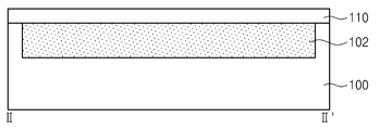
도 6 및 도 7을 참조하면, 기판(100)에 제 1 도전 영역(102)이 형성될 수 있다.Referring to FIGS. 6 and 7, a first
기판(100)은 반도체 기판이거나 반도체 근거 구조(semiconductor based structure)일 수 있다. 일 예로, 기판은 실리콘 기판 기판일 수 있다. 기판(100)에 제1 도전형의 불순물이 주입될 수 있다. 제 1 도전형은 n형 또는 p형일 수 있다. 제1 도전형의 불순물은 이온 주입 공정을 통해 기판(100)의 표면 부위에 도핑되고(doped), 도핑된 불순물을 확산시켜, 기판(100) 표면에 제 1 도전 영역(102)이 형성될 수 있다. The
제 1 도전 영역(102)이 형성된 기판(100) 상에 절연 마스크막(110)이 형성될 수 있다. 절연 마스크막(110)은 실리콘 산화물, 실리콘 질화물, 실리콘 산질화물 또는 금속 질화물을 포함할 수 있다. 이러한 절연 마스크막(110)은 화학 기상 증착(CVD) 공정 또는 물리 기상 증착(PVD) 공정에 의해 형성될 수 있다.The insulating
도 6 및 도 8을 참조하면, 기판(100) 상에 제 1 절연 마스크 패턴(112) 및 복수 개의 제 2 절연 마스크 패턴들(114)이 형성될 수 있다. Referring to FIGS. 6 and 8, a first insulating
제 1 및 제 2 절연 마스크 패턴들(112, 114)은 절연 마스크막(110) 상에 마스크 패턴(미도시)을 형성하고, 이를 식각 마스크로 하는 이방성 식각 공정이 수행되어 형성될 수 있다.The first and second insulating
제 1 절연 마스크 패턴(112)은 제 1 도전 영역(102)을 노출하는 개구부(115)를 가질 수 있고, 제 2 절연 마스크 패턴들(114)은 개구부(115) 내의 제 1 도전 영역(102) 상에 배치될 수 있다. 제 2 절연 마스크 패턴들(114)은 원기둥 형상일 수 있으나, 이에 제한되지 않으며 다각형의 기둥으로 형성될 수도 있다. The first insulating
제 2 절연 마스크 패턴들(114)은 제 1 방향(x 방향)으로 상호 이격되어 행을 이루는 제 1 그룹의 제 2 절연 마스크 패턴들(114)과 제 1 그룹으로부터 x 방향과 교차하는 제 2 방향(y 방향)으로 이격되는 제 2 그룹의 제 2 절연 마스크 패턴들(114)을 포함할 수 있다. 이러한 제 2 그룹의 제 2 절연 마스크 패턴들(114)은 x 방향으로 상호 이격되어 행을 이루되, 제 1 그룹의 제 2 절연 마스크 패턴들(114)로부터 x 방향으로 시프트(shift) 되어 배치될 수 있다. 이 때, 시프트(shift) 된 거리는 제 1 그룹의 제 2 절연 마스크 패턴들(114) 간의 피치(pitch)의 절반일 수 있다. 즉, 평면적 관점에서, 제 2 절연 마스크 패턴들(114)은 복수 개의 행과 열을 이루도록 배열될 수 있으며, 서로 인접하는 행들의 제 2 절연 마스크 패턴들(114)은 일 방향으로 지그재그 형태로 배열될 수 있다. 이에 따라, 제 2 절연 마스크 패턴들(114)은 개구부(115) 내에 최밀 충진 벌집 구조(closed packed honeycomb) 형태로 배열될 수 있다. The second
도 6 및 도 9를 참조하면, 제 1 및 제 2 절연 마스크 패턴들(112, 114) 사이로 노출되는 제 1 도전 영역(102)이 제거되어 개구부(115, 도 8 참조)가 기판(100) 내로 연장되는 리세스 영역(117)이 형성될 수 있다.6 and 9, the first
상세하게, 리세스 영역(117)은 제 1 및 제 2 절연 마스크 패턴들(112, 114)이 형성된 결과물 상에 이방성 식각 공정이 수행되어 형성될 수 있다. 이러한 식각 공정은 제 1 및 제 2 절연 마스크 패턴들(112, 114) 형성 시의 마스크 패턴(미도시)을 식각 마스크로 이용할 수 있다. 일 실시예에 있어서, 리세스 영역(117)의 형성을 위한 식각 공정은 제 1 및 제 2 절연 마스크 패턴들(112, 114)을 형성을 위한 식각 공정과 인-시튜(in-situ)로 수행될 수 있다. 이 때, 리세스 영역(117)의 하면은 제 1 도전 영역(102)의 하면 보다 높은 레벨일 수 있다.In detail, the recessed
리세스 영역(117)의 형성 결과, 기판(100)의 상부에 리세스 영역(117)에 의해 정의되는 돌출부들(104)이 형성될 수 있다. 이러한 돌출부들(104)은 제 2 절연 마스크 패턴들(114)과 동일한 형상으로 형성될 수 있으며, 리세스 영역(117) 내에서 제 2 절연 마스크 패턴들(114)과 동일한 배열을 이룰 수 있다. As a result of the formation of the recessed
도 6 및 도 10을 참조하면, 도 9의 결과물 상에 캡핑 차단막(120)이 형성될 수 있다.Referring to FIGS. 6 and 10, the
상세하게, 캡핑 차단막(120)은 제 1 및 제 2 절연 마스크 패턴들(112, 114)의 상면을 덮으며 리세스 영역(117) 내로 연장될 수 있다. 이러한 캡핑 차단막(120)은 비-콘포말하게(non-conformally) 형성될 수 있다. 즉, 제 1 및 제 2 절연 마스크 패턴들(112, 114)의 상면 상에 형성된 캡핑 차단막(120)의 두께는 리세스 영역(117) 내에 형성된 캡핑 차단막(120)의 두께보다 클 수 있다. In detail, the
캡핑 차단막(120)은 후술할 광 흡수층(140, 도 14 참조)의 형성 시 발생하는 관통 전위(treading dislocation) 결함을 차단할 수 있는 물질을 포함하되, 후술할 층간 절연막(130, 도 12 참조)과 식각 선택성을 갖는 물질을 포함할 수 있다. 일 예로, 캡핑 차단막(120)은 실리콘 질화물, 실리콘 산질화물 또는 금속 질화물을 포함할 수 있다. 이에 따라, 캡핑 차단막(120)은 제 1 및 제2 절연 마스크 패턴들(112, 114)과 동일한 물질 또는 다른 물질로 형성될 수 있다. 이러한 캡핑 차단막(120)은 화학 기상 증착(CVD) 공정 또는 물리 기상 증착(PVD) 공정에 의해 형성될 수 있다. The
도 6 및 도 11을 참조하면, 리세스 영역(117)의 하면에 형성된 캡핑 차단막(120, 도 10 참조)이 제거되어 제 1 캡핑 차단 패턴(122) 및 제 2 캡핑 차단 패턴들(124)이 형성될 수 있다.6 and 11, the capping blocking layer 120 (see FIG. 10) formed on the lower surface of the
상세하게, 제 1 및 제 2 캡핑 차단 패턴들(122, 124)은 캡핑 차단막(120, 도 10 참조)이 형성된 결과물 상에 이방성 식각 공정이 수행되어 형성될 수 있다. 제 1 및 제 2 절연 마스크 패턴들(112, 114) 상면의 캡핑 차단막(120, 도 10 참조)의 두께가 리세스 영역(117) 내의 캡핑 차단막(120, 도 10 참조)의 두께 보다 크기 때문에, 리세스 영역(117) 하면의 캡핑 차단막(120, 도 10 참조)이 제 1 도전 영역(102)을 노출하도록 식각 되어도 제 1 및 제 2 절연 마스크 패턴들(112, 114) 상면의 캡핑 차단막(120, 도 10 참조)은 잔류될 수 있다. 그 결과, 제 2 절연 마스크 패턴들(114) 및 제 2 캡핑 차단 패턴들(124)을 포함하는 전위 차단 패턴들(DP)이 형성될 수 있다. In detail, the first and second
전위 차단 패턴들(DP)은 전위 차단 패턴들(DP) 사이의 간격(S2) 대비 전위 차단 패턴들(DP)의 높이(H2)와 폭(W2)이 일정한 비율을 가지도록 형성될 수 있다. 즉, 전위 차단 패턴들(DP)은 이하에서 설명할 광 흡수층(140, 도 14 참조)의 형성 시 관통 전위 결함의 차단을 위해 전위 차단 패턴들(DP) 사이의 간격(S2) 대비 전위 차단 패턴(DP)의 높이(H2)의 비(aspect ratio)가 최소한 1 보다 크도록 형성될 수 있다. 일 예로, 전위 차단 패턴들(DP) 사이의 간격(S2) 대비 전위 패턴의 높이(H2)의 비는 1:1.1 ~ 1:4.4 값을 가질 수 있다. 이 때, 전위 차단 패턴들(DP) 사이의 간격(S2) 대비 전위 패턴의 폭(W2)의 비는 1:0.25 ~ 1:2의 값을 가질 수 있다.The potential blocking patterns DP may be formed such that the height H2 and the width W2 of the potential blocking patterns DP have a constant ratio with respect to the spacing S2 between the potential blocking patterns DP. That is, the potential blocking patterns DP are formed in the same manner as the potential blocking patterns DP in comparison with the gap S2 between the potential blocking patterns DP for blocking the threading dislocation defects when the light absorbing layer 140 (see FIG. 14) And the height H2 of the projection optical system DP is at least greater than one. For example, the ratio of the distance S2 between the potential blocking patterns DP to the height H2 of the potential pattern may have a value of 1: 1.1 to 1: 4.4. In this case, the ratio of the width S2 of the potential pattern to the width S2 of the potential blocking patterns DP may have a value of 1: 0.25 to 1: 2.
도 6 및 도 12를 참조하면, 제 1 및 제 2 캡핑 차단 패턴들(122, 124)이 형성된 리세스 영역(117)을 채우며 기판(100)의 전면을 덮는 층간 절연막(130)이 형성될 수 있다. 층간 절연막(130)은 제 1 및 제 2 캡핑 차단 패턴들(122, 124)과 식각 선택성이 있는 물질을 포함할 수 있다. 일 예로, 층간 절연막(130)은 실리콘 산화물을 포함할 수 있다. 이러한 층간 절연막(130)은 화학 기상 증착(CVD) 공정에 의해 형성될 수 있다.6 and 12, an
도 6 및 도 13을 참조하면, 제 1 캡핑 차단 패턴(122) 상에 전위 차단 패턴들(DP)을 노출하는 홈(135)을 갖는 층간 절연 패턴(132)이 형성될 수 있다.Referring to FIGS. 6 and 13, an interlayer
상세하게, 층간 절연 패턴(132)은 층간 절연막(130) 상에 마스크 패턴(미도시)을 형성하고, 이를 식각 마스크로 이용하는 건식 및/또는 습식 식각 공정이 수행되어 형성될 수 있다. 이러한 식각 공정의 결과, 리세스 영역(117)을 매립한 층간 절연막(130)이 제거되어 제 1 도전 영역(102)이 노출될 수 있다. In detail, the
일 실시예 따르면, 홈(135)에 의해 노출되는 층간 절연 패턴(132)은 경사진 측벽을 가질 수 있다. 즉, 층간 절연 패턴(132)의 홈(135)은 아래로 갈수록 실질적으로 좁아지는 폭을 가질 수 있다. 다른 실시예에 있어서, 홈(135)에 의해 노출되는 층간 절연 패턴(132)의 측면은 수직면을 가질 수 있다. 따라서, 층간 절연 패턴(132)의 홈(135)은 상부 및 하부가 실질적으로 동일한 폭을 가질 수 있다.According to one embodiment, the
도 6 및 도 14를 참조하면, 리세스 영역(117) 및 홈(135)을 매립하는 광 흡수층(140)이 형성될 수 있다. 이러한 광 흡수층(140)은 리세스 영역(117)을 채우며 캡핑 차단 패턴들(122, 124)의 상면을 덮는 제 1 영역(140a)과 제 1 영역(140a) 상의 제 2 영역(140b)을 포함할 수 있다.6 and 14, a
상세하게, 광 흡수층(140)의 제 1 영역(140a)은 리세스 영역(117) 내에 노출된 제 1 도전 영역(102)을 씨드층으로 하는 선택적 에피택셜 성장(selective epitaxial growth) 공정에 의해 형성될 수 있다. 성장 초기에 제 1 영역(140a)은 리세스 영역(117) 내의 제 1 도전 영역(102) 상에서만 형성되나, 성장이 진행될수록 측방으로(laterally) 과성장(overgrowth)되어 캡핑 차단 패턴들(122, 124)의 상면을 덮도록 형성될 수 있다. 이 후, 어닐링 공정(annealing) 공정이 수행될 수 있다. 이러한 어닐링 공정은 광 흡수층(140)의 용융점(melting point) 이하의 온도 조건에서 수행될 수 있다. 일 예로, 광 흡수층(140)이 게르마늄(Ge)을 포함하는 경우, 어닐링 공정은 수소(H2) 분위기 하에서 750 내지 900℃의 온도에서 수행될 수 있다. 어닐링 공정을 통해, 제 1 영역(140a)의 상면은 평탄화될 수 있으며, 제 1 영역(140a) 내의 결정 결함은 더욱 감소될 수 있다. 이어서, 홈(135)을 채우는 광 흡수층(140)의 제 2 영역(140b)이 형성될 수 있다. 제 2 영역(140b)은 제 1 영역(140a)을 씨드층으로 하는 에피택셜 성장(epitaxial growth) 공정에 의해 형성될 수 있다. 이러한 광 흡수층(140)은 실질적으로 단결정으로 성장될 수 있다. 일 예로, 광 흡수층(140)은 MBE(Molecular Beam Epitaxy), VPE(Vapor Phase Epitaxy), 또는 LPE(Liquid Phase Epitaxy)에 의하여 형성될 수 있다. 일 실시예에 있어서, 광 흡수층(140)은 게르마늄(Ge)을 포함할 수 있다. 광 흡수층(140)이 게르마늄을 포함하는 경우, 광 흡수층(140)의 형성을 위한 전구체로 GeH4, Ge2H6, GeH2Cl2, GeCl4, Ge2Cl6 등이 사용될 수 있다.The
단결정 실리콘 상에 직접적으로 게르마늄을 에픽택셜 성장(epitaxial growth)시킬 경우, 실리콘과 게르마늄 사이의 격자 상수 차이에 의해 자연적으로 결정 결함이 발생할 수 있다. 이러한 결정 결함은 광전 변환 효율을 떨어뜨리는 주된 요인이 된다. 하지만, 본 발명의 일 실시예 따르면, 리세스 영역(117) 내에 최밀 충진 벌집 구조 형태(closed packed honeycomb)로 배열된 전위 차단 패턴들(DP)을 형성함으로써, 초기의 게르마늄 성장시 발생되는 관통 전위(treading dislocation)가 전위 차단 패턴들(DP)에 의해 효과적으로 차단될 수 있다. 그 결과, 홈(135) 내에 측방으로 과성장된 게르마늄층은 리세스 영역(117) 내의 게르마늄층보다 관통 전위 밀도(treading dislocation density)가 현저하게 낮아질 수 있다. 즉, 광 흡수층(140)의 제 2 영역(140b)의 관통 전위 밀도는 제 1 영역(140a)의 관통 전위 밀도보다 현저히 낮을 수 있다.When epitaxial growth of germanium directly on monocrystalline silicon, crystal defects naturally occur due to the difference in lattice constant between silicon and germanium. These crystal defects are the main factors that lower the photoelectric conversion efficiency. However, according to one embodiment of the present invention, by forming disconnection blocking patterns DP arranged in a closed packed honeycomb structure in the recessed
도 6 및 도 15를 참조하면, 광 흡수층(140) 상에 제 2 도전 패턴(142)이 형성될 수 있다. Referring to FIGS. 6 and 15, a second
상세하게, 제 2 도전 패턴(142)은 광 흡수층(140)을 씨드층으로 하는 선택적 에피택셜 성장(selective epitaxial growth) 공정에 의해 형성될 수 있다. 이러한 제 2 도전 패턴(142)은 광 흡수층(140)과 동종 또는 이종의 반도체 물질을 포함할 수 있다. 일 실시예에 있어서, 제 2 도전 패턴(142)은 제 1 도전형과 다른 제 2 도전형의 불순물이 주입된 게르마늄층일 수 있다. 다른 실시예에 있어서, 제 2 도전 패턴(142)은 제2 도전형의 불순물이 포함된 실리콘층이거나 실리콘-게르마늄층일 수 있다. 불순물은 제 2 도전 패턴(142) 형성 후 이온 주입될 수도 있고, 제 2 도전 패턴(142)의 형성 시 인-시츄(in-situ)로 도핑될 수 있다. 도 14 및 도 15에서 설명된 광 흡수층(140) 및 제 2 도전 패턴(142)의 형성 공정은 실질적으로 동일한 챔버 내에서 즉, 인-시튜로 진행될 수 있다.In detail, the second
이어서, 층간 절연 패턴(132) 및 제 2 도전 패턴(142) 상에 콘포말하게 보호막(144)이 형성될 수 있다. 보호막(144)은 층간 절연 패턴(132) 및 제 2 도전 패턴(142)의 상부 프로파일(profile)을 따라 연속적으로 형성될 수 있다. 또한, 보호막(144)은 실리콘 산화물, 실리콘 질화물 또는 실리콘 산질화물을 포함할 수 있다.Then, a
계속해서 도 6 및 도 15를 참조하면, 제 1 도전 영역(102) 및 제 2 도전 패턴(142)과 각각 전기적으로 연결되는 제 1 및 제 2 연결 단자들(152, 154)이 형성될 수 있다. 제1 연결 단자들(152)은 보호막(144), 층간 절연 패턴(132), 제 1 캡핑 차단 패턴(122) 및 제 1 절연 마스크 패턴(112)을 관통하여 제 1 도전 영역(102)과 전기적으로 연결될 수 있다. 제 2 연결 단자들(154)은 보호막(144)을 관통하여 제 2 도전 패턴(142)과 전기적으로 연결될 수 있다. 본 실시예에서 제 1 및 제 2 연결 단자들(152, 154)을 각각 두 개로 도시하고 있으나, 본 발명에서, 제 1 및 제 2 연결 단자들(152, 154)의 수량을 한정하는 것은 아니다. 제 1 및 제 2 연결 단자들(152, 154)은 금속 또는 금속 화합물을 포함할 수 있다.Referring to FIGS. 6 and 15, first and
도 6 및 도 15를 다시 참조하며, 본 발명의 일 실시예에 따른 광 검출기(10)가 설명된다. Referring again to Figs. 6 and 15, a
본 발명의 일 실시예에 따른 광 검출기(10)는 기판(100) 상의 전위 차단 패턴들(DP)을 포함할 수 있다. 기판(100)은 반도체 기판이거나 반도체 근거 구조(semiconductor based structure)일 수 있다. 일 예로, 기판(100)은 실리콘 기판일 수 있다. 기판(100)은 제 1 도전 영역(102)을 포함할 수 있다. 제 1 도전 영역(102)은 제 1 도전형의 불순물이 주입된 영역일 수 있다. 제 1 도전형은 n형 또는 p형일 수 있다. The
기판(100)은 리세스 영역(117) 및 리세스 영역(117)에 의해 정의되는 돌출부들(104)을 가질 수 있다. 이러한 리세스 영역(117) 및 돌출부들(104)은 제 1 도전 영역(102)이 패터닝되어 형성된 부분일 수 있다. 돌출부들(104)은 원기둥 형상일 수 있으나, 이에 제한되지 않으며 다각형의 기둥 형상을 가질 수 있다. The
돌출부들(104)은 제 1 방향(이하 x 방향)으로 상호 이격되어 행을 이루는 제 1 그룹의 돌출부들(104)과 제 1 그룹으로부터 x 방향과 교차하는 제 2 방향(이하 y 방향)으로 이격되는 제 2 그룹의 돌출부들(104)을 포함할 수 있다. 이러한 제 2 그룹의 돌출부들(104)은 x 방향으로 상호 이격되어 행을 이루되, 제 1 그룹의 돌출부들(104)로부터 x 방향으로 시프트(shift) 되어 배치될 수 있다. 이 때, 시프트(shift) 된 거리는 제 1 그룹의 돌출부들(104) 간의 피치(pitch)의 절반일 수 있다. 즉, 평면적 관점에서, 돌출부들(104)은 리세스 영역(117) 내에서 복수 개의 행과 열을 이루도록 배열될 수 있으며, 서로 인접하는 행들의 돌출부들(104)은 일 방향으로 지그재그 형태로 배열될 수 있다. 이에 따라, 돌출부들(104)은 최밀 충진 벌집 구조(closed packed honeycomb) 형태로 배열될 수 있다.The
리세스 영역(117) 외의 기판(100) 상에 제 1 절연 마스크 패턴(112) 및 제 1 캡핑 차단 패턴(122)이 순차적으로 제공될 수 있다. 제 1 절연 마스크 패턴(112)은 리세스 영역(117) 및 돌출부들(104)을 노출할 수 있다. 제 1 캡핑 차단 패턴(122)은 제 1 절연 마스크 패턴(112)의 상부를 덮으며 제 1 절연 마스크 패턴(112)의 내측벽 및 리세스 영역(117)의 내측벽으로 연장될 수 있다. 제 1 절연 마스크 패턴(112)은 실리콘 산화물, 실리콘 질화물, 실리콘 산질화물 또는 금속 질화물을 포함할 수 있다. 제 1 캡핑 차단 패턴(122)은 실리콘 질화물, 실리콘 산질화물 또는 금속 질화물을 포함할 수 있다. 일 실시예에 있어서, 제 1 캡핑 차단 패턴(122)은 제 1 절연 마스크 패턴(112)과 동일한 물질로 형성될 수 있다. 일 예로, 제 1 절연 마스크 패턴(112)이 실리콘 질화물, 산질화물 또는 금속 질화물을 포함하는 경우, 제 1 캡핑 차단 패턴(122)은 제 1 절연 마스크 패턴(112)과 동일한 물질을 포함할 수 있다. 다른 실시예에 있어서 제 1 캡핑 차단 패턴(122)은 제 1 절연 마스크 패턴(112)과 다른 물질로 형성될 수 있다. 일 예로, 제 1 절연 마스크 패턴(112)이 실리콘 산화물을 포함하는 경우, 제 1 캡핑 차단 패턴(122)은 제 1 절연 마스크 패턴(112)과 다른 물질인 실리콘 질화물, 산질화물 또는 금속 질화물을 포함할 수 있다.A first insulating
돌출부들(104) 상에 제 2 절연 마스크 패턴들(114) 및 제 2 캡핑 차단 패턴들(124)이 제공될 수 있다. 제 2 절연 마스크 패턴들(114)은 돌출부들(104)과 동일한 형상을 가질 수 있고, 돌출부들(104)과 동일한 배열을 이룰 수 있다. 제 2 캡핑 차단 패턴들(124)은 제 2 절연 마스크 패턴들(114)의 상부를 덮으며, 제 2 절연 마스크 패턴들(114)의 외측벽 및 돌출부들(104)의 외측벽으로 연장될 수 있다. 제 2 절연 마스크 패턴들(114) 및 제 2 캡핑 차단 패턴들(124)은 각각 제 1 절연 마스크 패턴(112) 및 제 2 캡핑 차단 패턴들(124)과 동일한 물질을 포함할 수 있다. 이러한 제 2 절연 마스크 패턴들(114) 및 제 2 캡핑 차단 패턴들(124)은 전위 차단 패턴들(DP)을 구성할 수 있다. 결과적으로, 본 발명의 일 실시예에 따른 광 검출기(10)는 기판(100)의 리세스 영역(117) 상에 최밀 충진 벌집 구조(closed packed honeycomb) 형태로 배열되는 전위 차단 패턴들(DP)을 포함할 수 있다.The second
전위 차단 패턴들(DP)은 전위 차단 패턴들(DP) 사이의 간격(S2) 대비 일정한 높이(H2) 및 폭(W2)을 가질 수 있다. 즉, 광 흡수층(140)의 초기 형성 시 관통 전위 결함의 차단을 위해 전위 차단 패턴들(DP) 사이의 간격(S2)과 전위 패턴의 높이(H2)의 비(aspect ratio)는 최소한 1 보다 클 수 있다. 일 예로, 전위 차단 패턴들(DP) 사이의 간격(S2) 대비 전위 패턴의 높이(H2)의 비는 1:1.1 ~ 1:4.4의 값을 가질 수 있다. 이 때, 전위 차단 패턴들(DP) 사이의 간격(S2) 대비 전위 패턴의 폭(W2)의 비는 1:0.25 ~ 1:2의 값을 가질 수 있다.The potential blocking patterns DP may have a constant height H2 and a width W2 with respect to the interval S2 between the potential blocking patterns DP. That is, the aspect ratio of the interval S2 between the potential blocking patterns DP and the height H2 of the potential pattern for interrupting the threading dislocation defects during the initial formation of the
제 1 캡핑 차단 패턴들(122) 상에 층간 절연 패턴(132)이 배치될 수 있다. 층간 절연 패턴(132)은 제 1 및 제 2 캡핑 차단 패턴들(122, 124)과 식각 선택성이 있는 물질을 포함할 수 있다. 일 예로, 층간 절연 패턴(132)은 실리콘 산화물을 포함할 수 있다. An interlayer insulating
층간 절연 패턴(132)은 리세스 영역(117) 및 전위 차단 패턴들(DP)을 노출하는 홈(135)을 가질 수 있다. 평면적 관점에서, 층간 절연 패턴(132)의 홈(135)은 기판(100)의 리세스 영역(117)보다 넓은 면적을 가질 수 있다. 도 6에서 홈(135)은 원형으로 도시되었으나, 이에 제한되지 않는다. 일 실시예 따르면, 홈(135)에 의해 노출되는 층간 절연 패턴(132)은 경사진 측벽을 가질 수 있다. 즉, 층간 절연 패턴(132)의 홈(135)은 아래로 갈수록 실질적으로 좁아지는 폭을 가질 수 있다. 다른 실시예에 있어서, 홈(135)에 의해 노출되는 층간 절연 패턴(132)의 측면은 수직면을 가질 수 있다. 따라서, 층간 절연 패턴(132)의 홈(135)은 상부 및 하부가 실질적으로 동일한 폭을 가질 수 있다.The interlayer
전위 차단 패턴들(DP) 상에 층간 절연 패턴(132)의 홈(135)을 채우는 광 흡수층(140)이 배치될 수 있다. 이러한 광 흡수층(140)은 리세스 영역(117)을 채우며 전위 차단 패턴들(DP)의 상면을 덮는 제 1 영역(140a)과 제 1 영역(140a) 상의 제 2 영역(140b)을 포함할 수 있다. 광 흡수층(140)은 기판(100)과 1% 이상의 격자 상수 차이가 나는 4족 반도체 물질 또는 3-5족 화합물 반도체 물질을 포함할 수 있다. 일 예로, 광 흡수층(140)은 게르마늄(Ge)을 포함할 수 있다. 광 흡수층(140)은 실질적으로 도핑되지 않은 진성(intrinsic) 상태일 수 있다.A
기판(100)과 광 흡수층(140) 사이의 격자 상수 차이에 의해 광 흡수층(140) 내에 자연적으로 결정 결함이 발생할 수 있다. 본 실시예의 경우, 리세스 영역(117) 내의 광 흡수층(140)과 홈(135)을 채우는 광 흡수층(140)의 관통 전위 밀도(treading dislocation density)는 서로 다를 수 있다. 즉, 전위 차단 패턴들(DP)보다 높은 레벨에 위치하는 광 흡수층(140)의 제 2 영역(140b)의 관통 전위 밀도(treading dislocation density)는 제 1 영역(140a)의 관통 전위 밀도보다 현저히 낮을 수 있다. 이는 리세스 영역(117) 내에 전위 차단 패턴들(DP)을 최밀 충진 형태로 배열함으로써, 리세스 영역(117) 내의 광 흡수층(140)에서 발생되는 관통 전위(treading dislocation)가 전위 차단 패턴들(DP)에 의해 효과적으로 차단되었기 때문이다. 본 발명의 일 실시예에 따른 광 검출기(10)를 구성하는 기판(100) 및 광 흡수층(140)의 물질들은 각각 실리콘 및 게르마늄으로 설명되었으나, 이에 한정되지 않으며 본 발명의 사상 내에서 다양한 변형이 가능하다.A crystal defect may naturally occur in the
광 흡수층(140) 상에 제 2 도전 패턴(142)이 배치될 수 있다. 제 2 도전 패턴(142)은 광 흡수층(140)과 동종 또는 이종의 반도체 물질을 포함할 수 있다. 일 실시예에 있어서, 제 2 도전 패턴(142)은 제 1 도전형과 다른 제 2 도전형의 불순물이 주입된 게르마늄층일 수 있다. 다른 실시예에 있어서, 제 2 도전 패턴(142)은 제2 도전형의 불순물이 포함된 실리콘층이거나 실리콘-게르마늄층일 수 있다.The second
층간 절연 패턴(132) 및 제 2 도전 패턴(142) 상에 보호막(144)이 제공될 수 있다. 보호막(144)은 실리콘 산화물, 실리콘 질화물 또는 실리콘 산질화물을 포함할 수 있다. 제 1 도전 영역(102) 및 제 2 도전 패턴(142)과 각각 전기적으로 연결되는 제 1 및 제 2 연결 단자들(152, 154)이 제공될 수 있다. 제 1 연결 단자들(152)은 보호막(144), 층간 절연 패턴(132), 제 1 캡핑 차단 패턴(122) 및 제 1 절연 마스크 패턴(112)을 관통하여 제 1 도전 영역(102)과 전기적으로 연결될 수 있다. 제 2 연결 단자들(154)은 보호막(144)을 관통하여 제 2 도전 패턴(142)과 전기적으로 연결될 수 있다. 본 실시예에서 제 1 및 제 2 연결 단자들(152, 154)을 각각 두 개로 도시하고 있으나, 본 발명에서, 제 1 및 제 2 연결 단자들(152, 154)의 수량을 한정하는 것은 아니다. 제 1 및 제 2 연결 단자들(152, 154)은 금속 또는 금속 화합물을 포함할 수 있다.A
본 발명의 일 실시예에 따르면, 홈(135) 내에 제공되는 광 흡수층(140) 내의 전위 등 격자 결함의 밀도가 현저히 감소될 수 있다. 그 결과, 누설 전류에 의한 노이즈 증가 및 전하의 재결합 센터(recombination center)의 증가에 의한 신호 감소가 완화되어 광 검출기(10)의 반응성 및 민감도가 개선될 수 있다.According to one embodiment of the present invention, the density of dislocation lattice defects in the
또한, 본 발명의 일 실시예에 따른 광 검출기(10)는 광 흡수층(140) 하부의 기판(100)이 리세스 영역(117) 및 리세스 영역(117)에 의해 정의되는 돌출부들(104)를 포함하는 요철 구조를 가짐으로써 광 결합 효율이 증대되는 효과를 가질 수 있다.The
도 16은 본 발명의 다른 실시예에 따른 광 검출기를 설명하기 위한 단면도이다. 설명의 간소화를 위해 중복되는 구성의 설명은 생략한다. 도 16의 광 검출기(10-a)는 도 6 및 도 15의 리세스 영역과 제 1 및 제 2 절연 마스크 패턴들이 형성되지 않는 것을 제외하면 도 6 및 도 15의 광 검출기(10)와 실질적으로 동일할 수 있다.16 is a cross-sectional view illustrating a photodetector according to another embodiment of the present invention. For the sake of simplicity of description, a duplicate description of the configuration is omitted. The photodetector 10-a of FIG. 16 is substantially identical to the
도 6 및 도 16을 참조하면, 기판(100) 내의 제 1 도전 영역(102) 상에 전위 차단 패턴들(116, DP)이 배치될 수 있다. 전위 차단 패턴들(116, DP)은 원기둥 형상일 수 있으나, 이에 제한되지 않으며 다각형의 기둥 형상을 가질 수 있다. 이러한 전위 차단 패턴들(116, DP)은 도 15의 전위 차단 패턴들(DP)과 마찬가지로 최밀 충진 벌집 구조(closed packed honeycomb) 형태로 제 1 도전 영역(102) 상에 배열될 수 있다. 또한, 도 15에서의 전위 차단 패턴들(DP)과 마찬가지로 전위 차단 패턴들(116, DP)은 전위 차단 패턴들(116, DP) 사이의 간격(S3) 대비 일정한 높이(H3) 및 폭(W3)을 가질 수 있다. 즉, 광 흡수층(140)의 초기 형성 시 관통 전위 결함의 차단을 위해 전위 차단 패턴들(116, DP) 사이의 간격(S3) 대비 전위 차단 패턴들(116, DP)의 높이(H3)의 비(aspect ratio)는 최소한 1 보다 큰 것이 바람직하다. 일 예로, 전위 차단 패턴들(116, DP) 사이의 간격(S3) 대비 전위 차단 패턴들(116, DP)의 높이(H3)의 비는 1:1.1 ~ 1:4.4 의 값을 가질 수 있다. 이 때, 전위 차단 패턴들(116, DP) 사이의 간격(S3) 대비 전위 차단 패턴들(116, DP)의 폭(W3)의 비는 1:0.25 ~ 1:2의 값을 가질 수 있다. 전위 차단 패턴들(116, DP)은 도 15의 제 1 및 제 2 캡핑 차단 패턴들(122, 124)과 동일한 물질을 포함할 수 있다.6 and 16,
기판(100) 상에 층간 절연 패턴(132)이 배치될 수 있다. 층간 절연 패턴(132)은 전위 차단 패턴들(116, DP) 및 제 1 도전 영역(102)을 노출하는 홈(135)을 가질 수 있다. 평면적 관점에서, 층간 절연 패턴(132)의 홈(135)은 원형일 수 있으나 이에 제한되지 않는다. 층간 절연 패턴(132)은 전위 차단 패턴들(116, DP)과 식각 선택성이 있는 물질을 포함할 수 있다. 일 예로, 층간 절연 패턴(132)은 산화물을 포함할 수 있다. An interlayer insulating
제 1 도전 영역(102) 상에 홈(135)을 매립하는 광 흡수층(140)이 배치될 수 있다. 이러한 광 흡수층(140)은 전위 차단 패턴들(116, DP) 사이의 공간 및 전위 차단 패턴들(116, DP)과 층간 절연 패턴(132) 사이의 공간을 채우며 전위 차단 패턴들(116, DP)의 상면을 덮는 제 1 영역(140a)과 제 1 영역(140a) 상의 제 2 영역(140b)을 포함할 수 있다. 이 때, 전위 차단 패턴들(116, DP)보다 높은 레벨에 위치하는 광 흡수층(140)의 제 2 영역(140b)의 관통 전위 밀도는 제 1 영역(140a)의 관통 전위 밀도 보다 현저히 낮을 수 있다. 이는 도 15에서의 설명한 것과 마찬가지로, 제 1 도전 영역(102) 상에 전위 차단 패턴들(116, DP)을 최밀 충진 벌집 구조(closed packed honeycomb) 형태로 배열함으로써, 전위 차단 패턴들(116, DP) 사이의 공간 및 전위 차단 패턴들(116, DP)과 층간 절연 패턴(132) 사이의 공간의 광 흡수층(140)에서 발생되는 관통 전위(treading dislocation)가 전위 차단 패턴들(116, DP)에 의해 효과적으로 차단되었기 때문이다. A
도 17은 본 발명의 실시예들에 따른 광 검출기를 포함하는 전자 장치를 도식적으로 설명하기 위한 도면이다. 17 is a diagram for schematically explaining an electronic device including a photodetector according to embodiments of the present invention.
도 17을 참조하면, 본 발명의 실시예들에 따른 반도체 장치를 포함하는 전자 장치(1300)는 PDA, 랩톱(laptop) 컴퓨터, 휴대용 컴퓨터, 웹 태블릿(web tablet), 무선 전화기, 휴대폰, 디지털 음악 재생기(digital music player), 유무선 전자 기기 또는 이들 중의 적어도 둘을 포함하는 복합 전자 장치 중의 하나일 수 있다. 본 발명의 실시예들에 따른 전자 장치(1300)는 콘트롤러 (1310)와 메모리(1350를 연결하는 광 인터커넥션(1370)을 포함할 수 있다. 상기 광 인터커넥션(1380)은 콘트롤러(1310)로부터 전송 받은 데이터를 광 신호로 변환하는 옵티컬 트랜스미터(1320)와, 상기 옵티컬 트랜스미터(1320)로부터 전송받은 광 신호를 다시 전기적 신호로 변환하는 옵티컬 리시버(1330)를 포함할 수 있다. 본 발명의 실시예들에 따른 광 검출기는 상기 옵티컬 리시버(1330)의 일부를 구성할 수 있다. 본 발명의 실시예들에 따른 발광 소자는 상기 옵티컬 트랜스미터(1320)의 일부를 구성할 수 있다. 상기 옵티컬 리시버(1330)로부터 전송되는 신호는 앰프(1340)에 의하여 증폭될 수 있다. 콘트롤러(1310)는 예를 들면 하나 이상의 마이크로프로세서, 디지털 신호 프로세서, 마이크로 컨트롤러, 또는 이와 유사한 것들을 포함할 수 있다. 메모리(1330)는 예를 들면 콘트롤러(1310)에 의해 실행되는 명령어를 저장하는데 사용될 수 있다. 메모리(1330)는 사용자 데이터를 저장하는 데 사용될 수 있다. 17, an
상술된 실시예들에서 개시된 반도체 장치들은 다양한 형태들의 반도체 패키지(semiconductor package)로 구현될 수 있다. 예를 들면, 본 발명의 실시예들에 따른 반도체 장치들은 PoP(Package on Package), Ball grid arrays(BGAs), Chip scale packages(CSPs), Plastic Leaded Chip Carrier(PLCC), Plastic Dual In-Line Package(PDIP), Die in Waffle Pack, Die in Wafer Form, Chip On Board(COB), Ceramic Dual In-Line Package(CERDIP), Plastic Metric Quad Flat Pack(MQFP), Thin Quad Flatpack(TQFP), Small Outline(SOIC), Shrink Small Outline Package(SSOP), Thin Small Outline(TSOP), Thin Quad Flatpack(TQFP), System In Package(SIP), Multi Chip Package(MCP), Wafer-level Fabricated Package(WFP), Wafer-Level Processed Stack Package(WSP) 등의 방식으로 패키징될 수 있다.The semiconductor devices disclosed in the above embodiments can be implemented in various types of semiconductor packages. For example, the semiconductor devices according to the embodiments of the present invention may be used in a package on package (PoP), ball grid arrays (BGAs), chip scale packages (CSPs), plastic leaded chip carriers (PDIP), Die in Waffle Pack, Die in Wafer Form, Chip On Board (COB), Ceramic Dual In-Line Package (CERDIP), Plastic Metric Quad Flat Pack (MQFP), Thin Quad Flatpack (TQFP) SOIC), Shrink Small Outline Package (SSOP), Thin Small Outline (TSOP), Thin Quad Flatpack (TQFP), System In Package (SIP), Multi Chip Package (MCP), Wafer-level Fabricated Package Level Processed Stack Package (WSP) or the like.
이상의 발명의 상세한 설명은 개시된 실시 상태로 본 발명을 제한하려는 의도가 아니며, 본 발명의 요지를 벗어나지 않는 범위 내에서 다양한 다른 조합, 변경 및 환경에서 사용할 수 있다. 첨부된 청구범위는 다른 실시 상태도 포함하는 것으로 해석되어야 할 것이다.It is not intended to be exhaustive or to limit the invention to the precise form disclosed, and it will be apparent to those skilled in the art that various modifications and variations can be made in the present invention without departing from the spirit of the invention. The appended claims should be construed to include other embodiments.
Claims (10)
상기 돌출부들 상에 제공되고, 상기 돌출부들의 측벽으로 연장되는 제 1 절연 패턴들; 및
상기 리세스 영역을 채우며 상기 제 1 절연 패턴들을 덮는 제 2 반도체층을 포함하고,
상기 돌출부들은:
제 1 방향으로 상호 이격되어 행을 이루는 제 1 그룹의 돌출부들; 및
상기 제 1 그룹의 돌출부들로부터 상기 제 1 방향과 교차하는 제 2 방향으로 이격되되, 상기 제 1 방향으로 상호 이격되어 행을 이루는 제 2 그룹의 돌출부들을 포함하고,
상기 제 2 그룹의 돌출부들은 제 1 그룹의 돌출부들로부터 상기 제 1 방향으로 시프트 되어 배치되는 반도체 소자.A first semiconductor layer including protrusions defined by a recessed region and the recessed region;
First insulation patterns provided on the protrusions and extending to side walls of the protrusions; And
And a second semiconductor layer filling the recess region and covering the first insulating patterns,
The protrusions comprise:
A first group of protrusions spaced apart from each other in a first direction to form a row; And
A second group of protrusions spaced apart from the first group of protrusions in a second direction intersecting the first direction and spaced apart from each other in the first direction,
And the second group of protrusions are shifted and arranged in the first direction from the protrusions of the first group.
평면적 관점에서, 상기 돌출부들은 복수 개의 행과 열을 이루도록 배열되되, 서로 인접하는 상기 행들의 상기 돌출부들은 지그재그 형태로 배열되는 반도체 소자.The method according to claim 1,
In a plan view, the protrusions are arranged to form a plurality of rows and columns, and the protrusions of the rows adjacent to each other are arranged in a zigzag form.
상기 제 1 절연 패턴의 최하면으로부터 상기 제 1 절연 패턴의 상면까지의 높이는 상기 제 1 방향으로 인접한 제 1 절연 패턴들 사이의 간격보다 큰 반도체 소자.The method according to claim 1,
Wherein the height from the lowermost surface of the first insulation pattern to the upper surface of the first insulation pattern is greater than the gap between the first insulation patterns adjacent in the first direction.
상기 제 2 반도체층은 상기 리세스 영역을 채우는 제 1 부분과 상기 제 1 절연 패턴들의 상면보다 높은 레벨에 제공되는 제 2 부분을 포함하고,
상기 제 2 부분은 상기 제 1 부분보다 관통 전위 밀도가 낮은 반도체 소자.The method according to claim 1,
Wherein the second semiconductor layer includes a first portion filling the recess region and a second portion provided at a level higher than an upper surface of the first insulating patterns,
And the second portion has a lower threading dislocation density than the first portion.
상기 돌출부들 상에 제 1 절연 패턴들을 형성하는 것, 상기 제 1 절연 패턴들은 상기 돌출부들의 측벽으로 연장되고; 및
상기 리세스 영역을 채우며 상기 제 1 절연 패턴들을 덮는 제 2 반도체층을 형성하는 것을 포함하고,
상기 제 2 반도체층을 형성하는 것은;
상기 리세스 영역을 채우며 상기 제 1 절연 패턴들의 상면을 덮는 제 1 영역을 형성하는 것;
상기 제 1 영역의 형성 후에 어닐링 공정을 수행하는 것; 및
상기 어닐링 공정이 수행된 상기 제 1 영역 상에 제 2 영역을 형성하는 것을 포함하는 반도체 소자의 제조 방법.Forming a recessed region defining protrusions in the first semiconductor layer;
Forming first insulation patterns on the protrusions, the first insulation patterns extending to the sidewalls of the protrusions; And
Forming a second semiconductor layer filling the recess region and covering the first insulating patterns,
Forming the second semiconductor layer comprises:
Forming a first region filling the recessed region and covering an upper surface of the first insulating patterns;
Performing an annealing process after formation of the first region; And
And forming a second region on the first region on which the annealing process has been performed.
상기 돌출부들은:
제 1 방향으로 상호 이격되어 행을 이루는 제 1 그룹의 돌출부들; 및
상기 제 1 그룹의 돌출부들로부터 상기 제 1 방향과 교차하는 제 2 방향으로 이격되되, 상기 제 1 방향으로 상호 이격되어 행을 이루는 제 2 그룹의 돌출부들을 포함하고,
상기 제 2 그룹의 돌출부들은 제 1 그룹의 돌출부들로부터 상기 제 1 방향으로 시프트 되어 배치되는 반도체 소자의 제조 방법.6. The method of claim 5,
The protrusions comprise:
A first group of protrusions spaced apart from each other in a first direction to form a row; And
A second group of protrusions spaced apart from the first group of protrusions in a second direction intersecting the first direction and spaced apart from each other in the first direction,
And the second group of protrusions are shifted and arranged in the first direction from the protrusions of the first group.
평면적 관점에서, 상기 돌출부들은 복수 개의 행과 열을 이루도록 배열되되, 서로 인접하는 상기 행들의 상기 돌출부들은 지그재그 형태로 배열되는 반도체 소자의 제조 방법.The method according to claim 6,
In a plan view, the protrusions are arranged to form a plurality of rows and columns, and the protrusions of the rows adjacent to each other are arranged in a zigzag pattern.
상기 기판 상에 제공되고, 상기 기판을 노출하는 홈을 갖는 층간 절연 패턴;
상기 홈 내의 상기 기판 상에 제공되는 제 1 절연 패턴들; 및
상기 제 1 절연 패턴들 상에 제공되고 상기 홈을 매립하는 광 흡수층을 포함하고,
상기 제 1 절연 패턴들은:
제 1 방향으로 상호 이격되어 행을 이루는 제 1 그룹의 제 1 절연 패턴들; 및
상기 제 1 그룹의 제 1 절연 패턴들로부터 상기 제 1 방향과 교차하는 제 2 방향으로 이격되되, 상기 제 1 방향으로 상호 이격되어 행을 이루는 제 2 그룹의 제 1 절연 패턴들을 포함하고,
상기 제 2 그룹의 제 1 절연 패턴들은 상기 제 1 그룹의 제 1 절연 패턴들로부터 상기 제 1 방향으로 시프트 되어 배치되는 광 검출기.Board;
An interlayer insulating pattern provided on the substrate and having a groove exposing the substrate;
First insulation patterns provided on the substrate in the groove; And
And a light absorbing layer provided on the first insulating patterns and embedding the groove,
The first insulating patterns include:
A first group of first insulation patterns spaced apart from each other in a first direction; And
A first group of first insulation patterns spaced apart from the first group of first insulation patterns in a second direction intersecting with the first direction and spaced apart from each other in the first direction,
Wherein the first group of first insulation patterns are shifted from the first group of first insulation patterns in the first direction.
평면적 관점에서, 상기 제 1 절연 패턴들은 상기 홈 내에 복수 개의 행과 열을 이루도록 배열되되, 서로 인접하는 상기 행들의 상기 제 1 절연 패턴들은 지그재그 형태로 배열되는 광 검출기.9. The method of claim 8,
From a plan viewpoint, the first insulation patterns are arranged to form a plurality of rows and columns in the grooves, wherein the first insulation patterns of the rows adjacent to each other are arranged in a zigzag pattern.
상기 기판은 리세스 영역 및 상기 리세스 영역에 의해 정의되는 돌출부들을 더 포함하고,
상기 제 1 절연 패턴들은 상기 돌출부들 상에 제공되고 상기 돌출부들의 측벽으로 연장되는 광 검출기.9. The method of claim 8,
Wherein the substrate further comprises protrusions defined by a recessed region and the recessed region,
Wherein the first insulation patterns are provided on the protrusions and extend to the side walls of the protrusions.
Priority Applications (2)
| Application Number | Priority Date | Filing Date | Title |
|---|---|---|---|
| KR1020140026139A KR20150104420A (en) | 2014-03-05 | 2014-03-05 | Semiconductor device and method of fabricating the same |
| US14/582,294 US9537029B2 (en) | 2014-03-05 | 2014-12-24 | Semiconductor device with an epitaxial layer and method of fabricating the same |
Applications Claiming Priority (1)
| Application Number | Priority Date | Filing Date | Title |
|---|---|---|---|
| KR1020140026139A KR20150104420A (en) | 2014-03-05 | 2014-03-05 | Semiconductor device and method of fabricating the same |
Publications (1)
| Publication Number | Publication Date |
|---|---|
| KR20150104420A true KR20150104420A (en) | 2015-09-15 |
Family
ID=54018238
Family Applications (1)
| Application Number | Title | Priority Date | Filing Date |
|---|---|---|---|
| KR1020140026139A Withdrawn KR20150104420A (en) | 2014-03-05 | 2014-03-05 | Semiconductor device and method of fabricating the same |
Country Status (2)
| Country | Link |
|---|---|
| US (1) | US9537029B2 (en) |
| KR (1) | KR20150104420A (en) |
Families Citing this family (2)
| Publication number | Priority date | Publication date | Assignee | Title |
|---|---|---|---|---|
| TWI803556B (en) * | 2018-12-28 | 2023-06-01 | 晶元光電股份有限公司 | Semiconductor stack, semiconductor device and method for manufacturing the same |
| KR20230033407A (en) * | 2021-09-01 | 2023-03-08 | 삼성전자주식회사 | A reticle and method of forming patterns in a semiconductor device |
Family Cites Families (19)
| Publication number | Priority date | Publication date | Assignee | Title |
|---|---|---|---|---|
| KR100425457B1 (en) * | 2001-08-13 | 2004-03-30 | 삼성전자주식회사 | Semiconductor device having self-aligned contact pads and method for fabricating the same |
| ATE408850T1 (en) * | 2001-04-10 | 2008-10-15 | Harvard College | MICRO LENS FOR PROJECTION LITHOGRAPHY AND ITS PRODUCTION PROCESS |
| US6982217B2 (en) * | 2002-03-27 | 2006-01-03 | Canon Kabushiki Kaisha | Nano-structure and method of manufacturing nano-structure |
| EP3166152B1 (en) * | 2003-08-19 | 2020-04-15 | Nichia Corporation | Semiconductor light emitting diode and method of manufacturing its substrate |
| US8324660B2 (en) | 2005-05-17 | 2012-12-04 | Taiwan Semiconductor Manufacturing Company, Ltd. | Lattice-mismatched semiconductor structures with reduced dislocation defect densities and related methods for device fabrication |
| US7358107B2 (en) | 2005-10-27 | 2008-04-15 | Sharp Laboratories Of America, Inc. | Method of fabricating a germanium photo detector on a high quality germanium epitaxial overgrowth layer |
| FR2896337A1 (en) | 2006-01-17 | 2007-07-20 | St Microelectronics Crolles 2 | METHOD FOR MAKING A MONOCRYSTALLINE LAYER ON A DIELECTRIC LAYER |
| WO2008030574A1 (en) | 2006-09-07 | 2008-03-13 | Amberwave Systems Corporation | Defect reduction using aspect ratio trapping |
| CN101981703A (en) | 2008-02-15 | 2011-02-23 | 新加坡科技研究局 | Photodetector with valence-mending adsorbate region and a method of fabrication thereof |
| KR101101133B1 (en) | 2008-06-03 | 2012-01-05 | 삼성엘이디 주식회사 | Nitride single crystal growth method and nitride semiconductor light emitting device manufacturing method |
| US8507840B2 (en) * | 2010-12-21 | 2013-08-13 | Zena Technologies, Inc. | Vertically structured passive pixel arrays and methods for fabricating the same |
| US8384007B2 (en) * | 2009-10-07 | 2013-02-26 | Zena Technologies, Inc. | Nano wire based passive pixel image sensor |
| US9082673B2 (en) * | 2009-10-05 | 2015-07-14 | Zena Technologies, Inc. | Passivated upstanding nanostructures and methods of making the same |
| US8253211B2 (en) | 2008-09-24 | 2012-08-28 | Taiwan Semiconductor Manufacturing Company, Ltd. | Semiconductor sensor structures with reduced dislocation defect densities |
| KR101567976B1 (en) * | 2009-07-23 | 2015-11-11 | 삼성전자주식회사 | Semiconductor device |
| TWI562195B (en) | 2010-04-27 | 2016-12-11 | Pilegrowth Tech S R L | Dislocation and stress management by mask-less processes using substrate patterning and methods for device fabrication |
| US20120168823A1 (en) | 2010-12-31 | 2012-07-05 | Zhijiong Luo | Semiconductor device and method for manufacturing the same |
| US8481341B2 (en) | 2011-11-05 | 2013-07-09 | Tokyo Electron Limited | Epitaxial film growth in retrograde wells for semiconductor devices |
| US20130134309A1 (en) * | 2011-11-10 | 2013-05-30 | Yissum and Research Development Company of the Hebrew University of Jerusalem LTD. | Nonlinear optical and electro-optical devices and methods of use thereof for amplification of non-linear properties |
-
2014
- 2014-03-05 KR KR1020140026139A patent/KR20150104420A/en not_active Withdrawn
- 2014-12-24 US US14/582,294 patent/US9537029B2/en not_active Expired - Fee Related
Also Published As
| Publication number | Publication date |
|---|---|
| US20150255649A1 (en) | 2015-09-10 |
| US9537029B2 (en) | 2017-01-03 |
Similar Documents
| Publication | Publication Date | Title |
|---|---|---|
| US8697498B2 (en) | Methods of manufacturing three dimensional semiconductor memory devices using sub-plates | |
| US9997534B2 (en) | Vertical memory devices | |
| US10079203B2 (en) | Vertical memory devices and methods of manufacturing the same | |
| KR102783249B1 (en) | Vertical memory devices | |
| KR102533146B1 (en) | Three-dimensional semiconductor devices and method for fabricating the same | |
| KR102078852B1 (en) | Semiconductor devices and method of manufacturing the same | |
| US10804194B2 (en) | Semiconductor device and method of manufacturing the same | |
| KR102788248B1 (en) | Vertical memory devices and methods of manufacturing the same | |
| US10332900B2 (en) | Vertical memory devices | |
| KR20170090045A (en) | Vertical memory devices and methods of manufacturing the same | |
| KR20130103908A (en) | Semiconductor device with buried bit line and method for fabricating the same | |
| KR102815720B1 (en) | 3d memory device having a word line including polysilicon and metal and method of manufacturing same | |
| KR102831058B1 (en) | Semiconductor devices | |
| KR20180006817A (en) | Vertical memory devices | |
| TWI694544B (en) | Semiconductor device and method of preparing the same | |
| KR20200007261A (en) | Semiconductor Memory Device | |
| KR101915627B1 (en) | Thyristor random access memory device and method | |
| KR101223417B1 (en) | Semiconductor device and method of manufacturing thereof | |
| KR20130086778A (en) | Manufacturing method of vertical non-volatile memory device | |
| KR102698151B1 (en) | Vertical memory devices and methods of manufacturing the same | |
| KR102708558B1 (en) | Vertical memory devices | |
| KR20190123887A (en) | Semiconductor device and method of manufacturing the same | |
| KR20150104420A (en) | Semiconductor device and method of fabricating the same | |
| KR20100111528A (en) | Phase-changeable memory device and method of forming the same | |
| CN109494227B (en) | Semiconductor memory device and manufacturing method thereof |
Legal Events
| Date | Code | Title | Description |
|---|---|---|---|
| PA0109 | Patent application |
St.27 status event code: A-0-1-A10-A12-nap-PA0109 |
|
| R17-X000 | Change to representative recorded |
St.27 status event code: A-3-3-R10-R17-oth-X000 |
|
| PG1501 | Laying open of application |
St.27 status event code: A-1-1-Q10-Q12-nap-PG1501 |
|
| PC1203 | Withdrawal of no request for examination |
St.27 status event code: N-1-6-B10-B12-nap-PC1203 |
|
| WITN | Application deemed withdrawn, e.g. because no request for examination was filed or no examination fee was paid | ||
| P22-X000 | Classification modified |
St.27 status event code: A-2-2-P10-P22-nap-X000 |
|
| P22-X000 | Classification modified |
St.27 status event code: A-2-2-P10-P22-nap-X000 |