KR20150077765A - Method for pattering metallic nanowire-based transparent conductive film by surface treatment - Google Patents
Method for pattering metallic nanowire-based transparent conductive film by surface treatment Download PDFInfo
- Publication number
- KR20150077765A KR20150077765A KR1020130166586A KR20130166586A KR20150077765A KR 20150077765 A KR20150077765 A KR 20150077765A KR 1020130166586 A KR1020130166586 A KR 1020130166586A KR 20130166586 A KR20130166586 A KR 20130166586A KR 20150077765 A KR20150077765 A KR 20150077765A
- Authority
- KR
- South Korea
- Prior art keywords
- transparent conductive
- conductive film
- acid
- surface treatment
- metal
- Prior art date
- Legal status (The legal status is an assumption and is not a legal conclusion. Google has not performed a legal analysis and makes no representation as to the accuracy of the status listed.)
- Ceased
Links
- 239000002070 nanowire Substances 0.000 title claims abstract description 61
- 238000000034 method Methods 0.000 title claims abstract description 46
- 238000004381 surface treatment Methods 0.000 title claims abstract description 28
- 229910052751 metal Inorganic materials 0.000 claims abstract description 59
- 239000002184 metal Substances 0.000 claims abstract description 59
- 238000000059 patterning Methods 0.000 claims abstract description 25
- QTBSBXVTEAMEQO-UHFFFAOYSA-N Acetic acid Chemical compound CC(O)=O QTBSBXVTEAMEQO-UHFFFAOYSA-N 0.000 claims description 36
- 150000002978 peroxides Chemical class 0.000 claims description 18
- 229910044991 metal oxide Inorganic materials 0.000 claims description 17
- 150000004706 metal oxides Chemical class 0.000 claims description 17
- 239000000203 mixture Substances 0.000 claims description 17
- SUKJFIGYRHOWBL-UHFFFAOYSA-N sodium hypochlorite Chemical compound [Na+].Cl[O-] SUKJFIGYRHOWBL-UHFFFAOYSA-N 0.000 claims description 14
- 239000012756 surface treatment agent Substances 0.000 claims description 14
- 150000007524 organic acids Chemical class 0.000 claims description 12
- 229920005989 resin Polymers 0.000 claims description 11
- 239000011347 resin Substances 0.000 claims description 11
- 239000011230 binding agent Substances 0.000 claims description 10
- 150000007522 mineralic acids Chemical class 0.000 claims description 10
- 229910019093 NaOCl Inorganic materials 0.000 claims description 8
- XLOMVQKBTHCTTD-UHFFFAOYSA-N Zinc monoxide Chemical compound [Zn]=O XLOMVQKBTHCTTD-UHFFFAOYSA-N 0.000 claims description 8
- VEXZGXHMUGYJMC-UHFFFAOYSA-N Hydrochloric acid Chemical compound Cl VEXZGXHMUGYJMC-UHFFFAOYSA-N 0.000 claims description 6
- MUBZPKHOEPUJKR-UHFFFAOYSA-N Oxalic acid Chemical compound OC(=O)C(O)=O MUBZPKHOEPUJKR-UHFFFAOYSA-N 0.000 claims description 6
- OFOBLEOULBTSOW-UHFFFAOYSA-N Propanedioic acid Natural products OC(=O)CC(O)=O OFOBLEOULBTSOW-UHFFFAOYSA-N 0.000 claims description 6
- 150000002484 inorganic compounds Chemical class 0.000 claims description 5
- 229910010272 inorganic material Inorganic materials 0.000 claims description 5
- RLOWWWKZYUNIDI-UHFFFAOYSA-N phosphinic chloride Chemical compound ClP=O RLOWWWKZYUNIDI-UHFFFAOYSA-N 0.000 claims description 5
- NBIIXXVUZAFLBC-UHFFFAOYSA-N Phosphoric acid Chemical compound OP(O)(O)=O NBIIXXVUZAFLBC-UHFFFAOYSA-N 0.000 claims description 4
- 229940078916 carbamide peroxide Drugs 0.000 claims description 4
- 230000002708 enhancing effect Effects 0.000 claims description 4
- AMWRITDGCCNYAT-UHFFFAOYSA-L hydroxy(oxo)manganese;manganese Chemical compound [Mn].O[Mn]=O.O[Mn]=O AMWRITDGCCNYAT-UHFFFAOYSA-L 0.000 claims description 4
- JVTAAEKCZFNVCJ-UHFFFAOYSA-N lactic acid Chemical compound CC(O)C(O)=O JVTAAEKCZFNVCJ-UHFFFAOYSA-N 0.000 claims description 4
- XHXFXVLFKHQFAL-UHFFFAOYSA-N phosphoryl trichloride Chemical compound ClP(Cl)(Cl)=O XHXFXVLFKHQFAL-UHFFFAOYSA-N 0.000 claims description 4
- 229920002037 poly(vinyl butyral) polymer Polymers 0.000 claims description 4
- AQLJVWUFPCUVLO-UHFFFAOYSA-N urea hydrogen peroxide Chemical compound OO.NC(N)=O AQLJVWUFPCUVLO-UHFFFAOYSA-N 0.000 claims description 4
- 239000011787 zinc oxide Substances 0.000 claims description 4
- 239000004372 Polyvinyl alcohol Substances 0.000 claims description 3
- VYPSYNLAJGMNEJ-UHFFFAOYSA-N Silicium dioxide Chemical compound O=[Si]=O VYPSYNLAJGMNEJ-UHFFFAOYSA-N 0.000 claims description 3
- 229920002451 polyvinyl alcohol Polymers 0.000 claims description 3
- 229910052814 silicon oxide Inorganic materials 0.000 claims description 3
- PFUVRDFDKPNGAV-UHFFFAOYSA-N sodium peroxide Chemical group [Na+].[Na+].[O-][O-] PFUVRDFDKPNGAV-UHFFFAOYSA-N 0.000 claims description 3
- 239000004925 Acrylic resin Substances 0.000 claims description 2
- 229910020366 ClO 4 Inorganic materials 0.000 claims description 2
- GRYLNZFGIOXLOG-UHFFFAOYSA-N Nitric acid Chemical compound O[N+]([O-])=O GRYLNZFGIOXLOG-UHFFFAOYSA-N 0.000 claims description 2
- KDYFGRWQOYBRFD-UHFFFAOYSA-N Succinic acid Natural products OC(=O)CCC(O)=O KDYFGRWQOYBRFD-UHFFFAOYSA-N 0.000 claims description 2
- 229910000147 aluminium phosphate Inorganic materials 0.000 claims description 2
- KDYFGRWQOYBRFD-NUQCWPJISA-N butanedioic acid Chemical compound O[14C](=O)CC[14C](O)=O KDYFGRWQOYBRFD-NUQCWPJISA-N 0.000 claims description 2
- WUKWITHWXAAZEY-UHFFFAOYSA-L calcium difluoride Chemical compound [F-].[F-].[Ca+2] WUKWITHWXAAZEY-UHFFFAOYSA-L 0.000 claims description 2
- 229910001634 calcium fluoride Inorganic materials 0.000 claims description 2
- 229920002301 cellulose acetate Polymers 0.000 claims description 2
- 229920003086 cellulose ether Polymers 0.000 claims description 2
- 239000012461 cellulose resin Substances 0.000 claims description 2
- 239000004310 lactic acid Substances 0.000 claims description 2
- 235000014655 lactic acid Nutrition 0.000 claims description 2
- ORUIBWPALBXDOA-UHFFFAOYSA-L magnesium fluoride Chemical compound [F-].[F-].[Mg+2] ORUIBWPALBXDOA-UHFFFAOYSA-L 0.000 claims description 2
- 229910001635 magnesium fluoride Inorganic materials 0.000 claims description 2
- VZCYOOQTPOCHFL-UPHRSURJSA-N maleic acid Chemical compound OC(=O)\C=C/C(O)=O VZCYOOQTPOCHFL-UPHRSURJSA-N 0.000 claims description 2
- 239000011976 maleic acid Substances 0.000 claims description 2
- 229910017604 nitric acid Inorganic materials 0.000 claims description 2
- 235000006408 oxalic acid Nutrition 0.000 claims description 2
- KYKLWYKWCAYAJY-UHFFFAOYSA-N oxotin;zinc Chemical compound [Zn].[Sn]=O KYKLWYKWCAYAJY-UHFFFAOYSA-N 0.000 claims description 2
- 229920002635 polyurethane Polymers 0.000 claims description 2
- 239000004814 polyurethane Substances 0.000 claims description 2
- XOLBLPGZBRYERU-UHFFFAOYSA-N tin dioxide Chemical compound O=[Sn]=O XOLBLPGZBRYERU-UHFFFAOYSA-N 0.000 claims description 2
- 229910001887 tin oxide Inorganic materials 0.000 claims description 2
- VZCYOOQTPOCHFL-UHFFFAOYSA-N trans-butenedioic acid Natural products OC(=O)C=CC(O)=O VZCYOOQTPOCHFL-UHFFFAOYSA-N 0.000 claims description 2
- 238000002834 transmittance Methods 0.000 claims description 2
- 239000002105 nanoparticle Substances 0.000 claims 2
- 239000003795 chemical substances by application Substances 0.000 claims 1
- -1 salt compound Chemical class 0.000 abstract description 6
- 230000001590 oxidative effect Effects 0.000 abstract description 3
- 239000010408 film Substances 0.000 description 71
- 239000010410 layer Substances 0.000 description 38
- 239000000758 substrate Substances 0.000 description 25
- BQCADISMDOOEFD-UHFFFAOYSA-N Silver Chemical compound [Ag] BQCADISMDOOEFD-UHFFFAOYSA-N 0.000 description 12
- VLTRZXGMWDSKGL-UHFFFAOYSA-N perchloric acid Chemical compound OCl(=O)(=O)=O VLTRZXGMWDSKGL-UHFFFAOYSA-N 0.000 description 11
- 239000011248 coating agent Substances 0.000 description 9
- 238000000576 coating method Methods 0.000 description 9
- 239000002042 Silver nanowire Substances 0.000 description 8
- 230000000694 effects Effects 0.000 description 8
- 230000003287 optical effect Effects 0.000 description 8
- 239000011241 protective layer Substances 0.000 description 8
- 239000004615 ingredient Substances 0.000 description 7
- LFQSCWFLJHTTHZ-UHFFFAOYSA-N Ethanol Chemical compound CCO LFQSCWFLJHTTHZ-UHFFFAOYSA-N 0.000 description 6
- 238000005530 etching Methods 0.000 description 6
- 238000004519 manufacturing process Methods 0.000 description 6
- 230000007613 environmental effect Effects 0.000 description 5
- 229920000139 polyethylene terephthalate Polymers 0.000 description 5
- 239000005020 polyethylene terephthalate Substances 0.000 description 5
- 229920002153 Hydroxypropyl cellulose Polymers 0.000 description 4
- XEEYBQQBJWHFJM-UHFFFAOYSA-N Iron Chemical compound [Fe] XEEYBQQBJWHFJM-UHFFFAOYSA-N 0.000 description 4
- 150000001875 compounds Chemical class 0.000 description 4
- 239000010949 copper Substances 0.000 description 4
- 239000001863 hydroxypropyl cellulose Substances 0.000 description 4
- 235000010977 hydroxypropyl cellulose Nutrition 0.000 description 4
- 239000002346 layers by function Substances 0.000 description 4
- 238000002360 preparation method Methods 0.000 description 4
- RYGMFSIKBFXOCR-UHFFFAOYSA-N Copper Chemical compound [Cu] RYGMFSIKBFXOCR-UHFFFAOYSA-N 0.000 description 3
- ATJFFYVFTNAWJD-UHFFFAOYSA-N Tin Chemical compound [Sn] ATJFFYVFTNAWJD-UHFFFAOYSA-N 0.000 description 3
- HCHKCACWOHOZIP-UHFFFAOYSA-N Zinc Chemical compound [Zn] HCHKCACWOHOZIP-UHFFFAOYSA-N 0.000 description 3
- 229910052802 copper Inorganic materials 0.000 description 3
- 238000009413 insulation Methods 0.000 description 3
- 239000000463 material Substances 0.000 description 3
- 150000002739 metals Chemical class 0.000 description 3
- 229910052709 silver Inorganic materials 0.000 description 3
- 239000004332 silver Substances 0.000 description 3
- 239000011135 tin Substances 0.000 description 3
- 229910052718 tin Inorganic materials 0.000 description 3
- XLYOFNOQVPJJNP-UHFFFAOYSA-N water Chemical compound O XLYOFNOQVPJJNP-UHFFFAOYSA-N 0.000 description 3
- 229910052725 zinc Inorganic materials 0.000 description 3
- 239000011701 zinc Substances 0.000 description 3
- XTEGARKTQYYJKE-UHFFFAOYSA-M Chlorate Chemical compound [O-]Cl(=O)=O XTEGARKTQYYJKE-UHFFFAOYSA-M 0.000 description 2
- 229920000089 Cyclic olefin copolymer Polymers 0.000 description 2
- PXHVJJICTQNCMI-UHFFFAOYSA-N Nickel Chemical compound [Ni] PXHVJJICTQNCMI-UHFFFAOYSA-N 0.000 description 2
- KDLHZDBZIXYQEI-UHFFFAOYSA-N Palladium Chemical compound [Pd] KDLHZDBZIXYQEI-UHFFFAOYSA-N 0.000 description 2
- 239000004642 Polyimide Substances 0.000 description 2
- 230000002411 adverse Effects 0.000 description 2
- 229910052782 aluminium Inorganic materials 0.000 description 2
- XAGFODPZIPBFFR-UHFFFAOYSA-N aluminium Chemical compound [Al] XAGFODPZIPBFFR-UHFFFAOYSA-N 0.000 description 2
- 230000015572 biosynthetic process Effects 0.000 description 2
- 239000008199 coating composition Substances 0.000 description 2
- 239000004020 conductor Substances 0.000 description 2
- 238000007796 conventional method Methods 0.000 description 2
- 238000005336 cracking Methods 0.000 description 2
- 239000012153 distilled water Substances 0.000 description 2
- 230000001747 exhibiting effect Effects 0.000 description 2
- PCHJSUWPFVWCPO-UHFFFAOYSA-N gold Chemical compound [Au] PCHJSUWPFVWCPO-UHFFFAOYSA-N 0.000 description 2
- 229910052737 gold Inorganic materials 0.000 description 2
- 239000010931 gold Substances 0.000 description 2
- WQYVRQLZKVEZGA-UHFFFAOYSA-N hypochlorite Chemical compound Cl[O-] WQYVRQLZKVEZGA-UHFFFAOYSA-N 0.000 description 2
- 230000001965 increasing effect Effects 0.000 description 2
- 239000012212 insulator Substances 0.000 description 2
- 229910052742 iron Inorganic materials 0.000 description 2
- BASFCYQUMIYNBI-UHFFFAOYSA-N platinum Chemical compound [Pt] BASFCYQUMIYNBI-UHFFFAOYSA-N 0.000 description 2
- 229920001721 polyimide Polymers 0.000 description 2
- 230000003014 reinforcing effect Effects 0.000 description 2
- 230000001052 transient effect Effects 0.000 description 2
- DEXFNLNNUZKHNO-UHFFFAOYSA-N 6-[3-[4-[2-(2,3-dihydro-1H-inden-2-ylamino)pyrimidin-5-yl]piperidin-1-yl]-3-oxopropyl]-3H-1,3-benzoxazol-2-one Chemical compound C1C(CC2=CC=CC=C12)NC1=NC=C(C=N1)C1CCN(CC1)C(CCC1=CC2=C(NC(O2)=O)C=C1)=O DEXFNLNNUZKHNO-UHFFFAOYSA-N 0.000 description 1
- 229920002134 Carboxymethyl cellulose Polymers 0.000 description 1
- 229920002284 Cellulose triacetate Polymers 0.000 description 1
- 239000001856 Ethyl cellulose Substances 0.000 description 1
- ZZSNKZQZMQGXPY-UHFFFAOYSA-N Ethyl cellulose Chemical compound CCOCC1OC(OC)C(OCC)C(OCC)C1OC1C(O)C(O)C(OC)C(CO)O1 ZZSNKZQZMQGXPY-UHFFFAOYSA-N 0.000 description 1
- MHAJPDPJQMAIIY-UHFFFAOYSA-N Hydrogen peroxide Chemical compound OO MHAJPDPJQMAIIY-UHFFFAOYSA-N 0.000 description 1
- 229920000663 Hydroxyethyl cellulose Polymers 0.000 description 1
- 239000004354 Hydroxyethyl cellulose Substances 0.000 description 1
- FYYHWMGAXLPEAU-UHFFFAOYSA-N Magnesium Chemical compound [Mg] FYYHWMGAXLPEAU-UHFFFAOYSA-N 0.000 description 1
- AFCARXCZXQIEQB-UHFFFAOYSA-N N-[3-oxo-3-(2,4,6,7-tetrahydrotriazolo[4,5-c]pyridin-5-yl)propyl]-2-[[3-(trifluoromethoxy)phenyl]methylamino]pyrimidine-5-carboxamide Chemical compound O=C(CCNC(=O)C=1C=NC(=NC=1)NCC1=CC(=CC=C1)OC(F)(F)F)N1CC2=C(CC1)NN=N2 AFCARXCZXQIEQB-UHFFFAOYSA-N 0.000 description 1
- NNLVGZFZQQXQNW-ADJNRHBOSA-N [(2r,3r,4s,5r,6s)-4,5-diacetyloxy-3-[(2s,3r,4s,5r,6r)-3,4,5-triacetyloxy-6-(acetyloxymethyl)oxan-2-yl]oxy-6-[(2r,3r,4s,5r,6s)-4,5,6-triacetyloxy-2-(acetyloxymethyl)oxan-3-yl]oxyoxan-2-yl]methyl acetate Chemical compound O([C@@H]1O[C@@H]([C@H]([C@H](OC(C)=O)[C@H]1OC(C)=O)O[C@H]1[C@@H]([C@@H](OC(C)=O)[C@H](OC(C)=O)[C@@H](COC(C)=O)O1)OC(C)=O)COC(=O)C)[C@@H]1[C@@H](COC(C)=O)O[C@@H](OC(C)=O)[C@H](OC(C)=O)[C@H]1OC(C)=O NNLVGZFZQQXQNW-ADJNRHBOSA-N 0.000 description 1
- 238000005299 abrasion Methods 0.000 description 1
- 150000001242 acetic acid derivatives Chemical class 0.000 description 1
- 239000001768 carboxy methyl cellulose Substances 0.000 description 1
- 235000010948 carboxy methyl cellulose Nutrition 0.000 description 1
- 239000008112 carboxymethyl-cellulose Substances 0.000 description 1
- 229920002678 cellulose Polymers 0.000 description 1
- 239000001913 cellulose Substances 0.000 description 1
- 229910001919 chlorite Inorganic materials 0.000 description 1
- 229910052619 chlorite group Inorganic materials 0.000 description 1
- QBWCMBCROVPCKQ-UHFFFAOYSA-N chlorous acid Chemical compound OCl=O QBWCMBCROVPCKQ-UHFFFAOYSA-N 0.000 description 1
- 230000000052 comparative effect Effects 0.000 description 1
- 239000002131 composite material Substances 0.000 description 1
- 229920001577 copolymer Polymers 0.000 description 1
- 230000002542 deteriorative effect Effects 0.000 description 1
- 229920005994 diacetyl cellulose Polymers 0.000 description 1
- 239000006185 dispersion Substances 0.000 description 1
- 229920001249 ethyl cellulose Polymers 0.000 description 1
- 235000019325 ethyl cellulose Nutrition 0.000 description 1
- 239000012530 fluid Substances 0.000 description 1
- 239000007789 gas Substances 0.000 description 1
- QOSATHPSBFQAML-UHFFFAOYSA-N hydrogen peroxide;hydrate Chemical compound O.OO QOSATHPSBFQAML-UHFFFAOYSA-N 0.000 description 1
- 235000019447 hydroxyethyl cellulose Nutrition 0.000 description 1
- 239000001866 hydroxypropyl methyl cellulose Substances 0.000 description 1
- 229920003088 hydroxypropyl methyl cellulose Polymers 0.000 description 1
- 235000010979 hydroxypropyl methyl cellulose Nutrition 0.000 description 1
- UFVKGYZPFZQRLF-UHFFFAOYSA-N hydroxypropyl methyl cellulose Chemical group OC1C(O)C(OC)OC(CO)C1OC1C(O)C(O)C(OC2C(C(O)C(OC3C(C(O)C(O)C(CO)O3)O)C(CO)O2)O)C(CO)O1 UFVKGYZPFZQRLF-UHFFFAOYSA-N 0.000 description 1
- 238000007654 immersion Methods 0.000 description 1
- 230000001771 impaired effect Effects 0.000 description 1
- 229910052738 indium Inorganic materials 0.000 description 1
- APFVFJFRJDLVQX-UHFFFAOYSA-N indium atom Chemical compound [In] APFVFJFRJDLVQX-UHFFFAOYSA-N 0.000 description 1
- 239000011254 layer-forming composition Substances 0.000 description 1
- 239000004973 liquid crystal related substance Substances 0.000 description 1
- 229910052749 magnesium Inorganic materials 0.000 description 1
- 239000011777 magnesium Substances 0.000 description 1
- 239000012528 membrane Substances 0.000 description 1
- 229920000609 methyl cellulose Polymers 0.000 description 1
- 239000001923 methylcellulose Substances 0.000 description 1
- 235000010981 methylcellulose Nutrition 0.000 description 1
- 125000005487 naphthalate group Chemical group 0.000 description 1
- 229910052759 nickel Inorganic materials 0.000 description 1
- KBJMLQFLOWQJNF-UHFFFAOYSA-N nickel(ii) nitrate Chemical class [Ni+2].[O-][N+]([O-])=O.[O-][N+]([O-])=O KBJMLQFLOWQJNF-UHFFFAOYSA-N 0.000 description 1
- 229910052763 palladium Inorganic materials 0.000 description 1
- 230000035515 penetration Effects 0.000 description 1
- VLTRZXGMWDSKGL-UHFFFAOYSA-M perchlorate Inorganic materials [O-]Cl(=O)(=O)=O VLTRZXGMWDSKGL-UHFFFAOYSA-M 0.000 description 1
- JRKICGRDRMAZLK-UHFFFAOYSA-L peroxydisulfate Chemical compound [O-]S(=O)(=O)OOS([O-])(=O)=O JRKICGRDRMAZLK-UHFFFAOYSA-L 0.000 description 1
- 238000000206 photolithography Methods 0.000 description 1
- 230000000704 physical effect Effects 0.000 description 1
- 229910052697 platinum Inorganic materials 0.000 description 1
- 229920000515 polycarbonate Polymers 0.000 description 1
- 239000004417 polycarbonate Substances 0.000 description 1
- 229920005996 polystyrene-poly(ethylene-butylene)-polystyrene Polymers 0.000 description 1
- 229920001290 polyvinyl ester Polymers 0.000 description 1
- 229920000036 polyvinylpyrrolidone Polymers 0.000 description 1
- 239000001267 polyvinylpyrrolidone Substances 0.000 description 1
- 235000013855 polyvinylpyrrolidone Nutrition 0.000 description 1
- 230000002787 reinforcement Effects 0.000 description 1
- 150000003839 salts Chemical class 0.000 description 1
- LIVNPJMFVYWSIS-UHFFFAOYSA-N silicon monoxide Chemical class [Si-]#[O+] LIVNPJMFVYWSIS-UHFFFAOYSA-N 0.000 description 1
- 238000004528 spin coating Methods 0.000 description 1
- 238000005507 spraying Methods 0.000 description 1
- 238000005728 strengthening Methods 0.000 description 1
- 239000000126 substance Substances 0.000 description 1
- 239000006228 supernatant Substances 0.000 description 1
- 239000002562 thickening agent Substances 0.000 description 1
- 239000010409 thin film Substances 0.000 description 1
- 150000003568 thioethers Chemical class 0.000 description 1
Images


Classifications
-
- H—ELECTRICITY
- H01—ELECTRIC ELEMENTS
- H01B—CABLES; CONDUCTORS; INSULATORS; SELECTION OF MATERIALS FOR THEIR CONDUCTIVE, INSULATING OR DIELECTRIC PROPERTIES
- H01B5/00—Non-insulated conductors or conductive bodies characterised by their form
- H01B5/14—Non-insulated conductors or conductive bodies characterised by their form comprising conductive layers or films on insulating-supports
-
- B—PERFORMING OPERATIONS; TRANSPORTING
- B82—NANOTECHNOLOGY
- B82Y—SPECIFIC USES OR APPLICATIONS OF NANOSTRUCTURES; MEASUREMENT OR ANALYSIS OF NANOSTRUCTURES; MANUFACTURE OR TREATMENT OF NANOSTRUCTURES
- B82Y10/00—Nanotechnology for information processing, storage or transmission, e.g. quantum computing or single electron logic
-
- B—PERFORMING OPERATIONS; TRANSPORTING
- B82—NANOTECHNOLOGY
- B82Y—SPECIFIC USES OR APPLICATIONS OF NANOSTRUCTURES; MEASUREMENT OR ANALYSIS OF NANOSTRUCTURES; MANUFACTURE OR TREATMENT OF NANOSTRUCTURES
- B82Y30/00—Nanotechnology for materials or surface science, e.g. nanocomposites
-
- G—PHYSICS
- G02—OPTICS
- G02B—OPTICAL ELEMENTS, SYSTEMS OR APPARATUS
- G02B1/00—Optical elements characterised by the material of which they are made; Optical coatings for optical elements
- G02B1/10—Optical coatings produced by application to, or surface treatment of, optical elements
-
- H—ELECTRICITY
- H01—ELECTRIC ELEMENTS
- H01B—CABLES; CONDUCTORS; INSULATORS; SELECTION OF MATERIALS FOR THEIR CONDUCTIVE, INSULATING OR DIELECTRIC PROPERTIES
- H01B13/00—Apparatus or processes specially adapted for manufacturing conductors or cables
-
- H—ELECTRICITY
- H10—SEMICONDUCTOR DEVICES; ELECTRIC SOLID-STATE DEVICES NOT OTHERWISE PROVIDED FOR
- H10D—INORGANIC ELECTRIC SEMICONDUCTOR DEVICES
- H10D64/00—Electrodes of devices having potential barriers
- H10D64/20—Electrodes characterised by their shapes, relative sizes or dispositions
- H10D64/205—Nanosized electrodes, e.g. nanowire electrodes
Landscapes
- Engineering & Computer Science (AREA)
- Chemical & Material Sciences (AREA)
- Nanotechnology (AREA)
- Physics & Mathematics (AREA)
- General Physics & Mathematics (AREA)
- Crystallography & Structural Chemistry (AREA)
- Materials Engineering (AREA)
- Optics & Photonics (AREA)
- Condensed Matter Physics & Semiconductors (AREA)
- Composite Materials (AREA)
- Mathematical Physics (AREA)
- Theoretical Computer Science (AREA)
- Manufacturing & Machinery (AREA)
- Non-Insulated Conductors (AREA)
- Laminated Bodies (AREA)
- Manufacturing Of Printed Circuit Boards (AREA)
Abstract
본 발명은 표면처리를 통한 금속 나노와이어 기반 투명 전도성 막의 패터닝 방법에 관한 것으로, 보다 상세하게는, 패턴닝 공정 전에 광학 기능층을 추가하여 굴절율을 조절하고, 표면처리제 조성물을 이용하여 금속 나노와이어 투명 전도성 막의 표면을 산화시키거나 염 화합물을 생성시켜 색상을 변화시킴으로써 표면을 절연시키고, 시인성이 우수한 막을 패터닝하는 방법에 관한 것이다.The present invention relates to a method of patterning a transparent conductive film based on a metal nanowire through surface treatment, and more particularly, to a method of patterning a transparent conductive film using a metal nanowire transparent The present invention relates to a method of patterning a film having excellent visibility by oxidizing the surface of a conductive film or generating a salt compound to change the color.
Description
본 발명은 표면처리를 통한 금속 나노와이어 기반 투명 전도성 막의 패터닝 방법에 관한 것으로, 보다 상세하게는, 패터닝 공정 전에 성능 강화층을 추가하여 굴절율을 조절하고, 표면처리제를 이용하여 금속 나노와이어 투명 전도성 막의 표면을 산화시키거나 염 화합물을 생성시켜 색상을 변화시킴으로써 표면을 절연시키고, 시인성이 우수한 막을 패터닝하는 방법에 관한 것이다.
The present invention relates to a method of patterning a metal nanowire-based transparent conductive film by surface treatment, and more particularly, to a method of patterning a metal nanowire transparent conductive film using a surface treatment agent, To a method of patterning a film having excellent visibility by oxidizing the surface or generating a salt compound to change the color.
ITO는 일반적으로 투명전도성 필름으로 터치스크린패널, OLED 소자, 유연소자 등에 활발히 적용되고 있지만, 기판이 대형화될수록 요구되는 낮은 면저항 및 우수한 유연성 등을 만족시키기에는 금속 산화물이라는 한계로 인하여 대체물질이 절실히 요청되고 있다. ITO is generally applied to touch screen panels, OLED devices, flexible devices and the like as a transparent conductive film. However, in order to satisfy the required low sheet resistance and excellent flexibility as the substrate is enlarged, a substitute material is desperately required .
이런 문제를 해결하기 위한 대체 재료로써 금속 나노와이어 기반 투명 전도성 필름이 쓰이고 있으며, ITO에서 해결하지 못하는 필름에서의 높은 광학적인 특성을 유지하면서 낮은 면저항을 구현하고 우수한 유연성을 지니고 있어 다양한 분야에서 쓰이고 있다. Transparent conductive films based on metal nanowires are used as alternative materials to solve this problem. They are used in various fields because they have low optical properties, high flexibility, and high optical properties in films that can not be solved by ITO .
하지만, 금속 나노와이어 기반 투명전도성 필름은 ITO와 다르게 에칭 공정을 거쳐서 패터닝을 진행하였을 경우 시인성이 안 좋은 단점이 있다. 종래의 ITO 필름에서는 ITO 자체의 높은 굴절률을 조절하기 위한 많은 노력이 있었지만, 금속 나노와이어의 경우에는 굴절률 보다는 금속에서 반사되는 빛의 산란에 의한 헤이즈 등이 시인성에 영향을 많이 주는 인자로 알려져 있으며, 실제 은 나노와이어의 경우에는 이러한 헤이즈가 에칭부와 비에칭부에서 차이가 나면서 패턴이 사람 눈에 쉽게 인식되는 문제가 발생하고 있다. However, the transparent conductive film based on the metal nanowire has a disadvantage that visibility is poor when the patterning is performed through the etching process differently from the ITO. In conventional ITO films, there has been a great deal of effort to control the refractive index of ITO itself. However, in the case of metal nanowires, haze due to scattering of light reflected by metals rather than refractive index is known to be a factor affecting visibility. Actually, in the case of a nanowire, the haze differs between the etched portion and the non-etched portion, and the pattern is easily recognized by the human eye.
기존의 금속 나노와이어로 구성된 투명 전도성 막의 경우에는, 이러한 시인성에 대한 고려 없이 에칭 공정을 통하여 패턴을 형성하고 에칭면이나 에칭면의 배면에 반사 방지막 등을 추가로 형성하여 에칭면과 비에칭면의 굴절율 또는 헤이즈 특성을 조절하는 시도가 있었으나, 에칭면과 비에칭면의 구분 없이 반사 방지막을 형성할 경우 비에칭면에도 동일한 반사방지 효과를 부여하기 때문에 시인성 확보에 뛰어난 효과를 가지지 못한다.In the case of a transparent conductive film composed of conventional metal nanowires, a pattern is formed through an etching process without considering the visibility, and an antireflection film or the like is additionally formed on the back surface of the etching surface or the etching surface, An attempt has been made to adjust the refractive index or haze characteristic. However, when the antireflection film is formed without distinguishing between the etched surface and the non-etched surface, the same antireflection effect is imparted to the non-etched surface.
금속 나노와이어 기반 투명전도성 막에서 패터닝 후 추가적인 광학 기능층의 구성없이 시인성을 확보하기 위해서는 최대한 패턴부와 비패턴부 간의 광학적인 특성 차이를 최소화하여야 한다. 특히, 헤이즈 특성은 금속 나노와이어 기반에서 시인성 특성에 영향을 가장 많이 미치는 인자로 패턴부와 비패턴부간의 헤이즈 차이를 줄여야 한다.In order to ensure visibility without patterning additional optical functional layers after patterning in a metal nanowire-based transparent conductive film, the optical characteristic difference between the pattern portion and the non-pattern portion should be minimized. In particular, the haze characteristic is the most influential factor on the visibility characteristic in the metal nanowire base, and the haze difference between the pattern portion and the non-pattern portion should be reduced.
이에, 상기와 같은 문제점을 해결하기 위해, 본 발명은 패터닝 공정 전에 광학 기능층을 추가하여 굴절율을 조절하고, 표면처리제를 이용하여 금속 나노와이어 투명 전도성 막의 표면을 산화시키거나 염 화합물을 생성시켜 색상을 변화시킴으로써 표면을 절연시키고, 시인성이 우수한 막을 패터닝하는 방법을 제공하는 것을 목적으로 한다.In order to solve the above-described problems, the present invention provides a method of manufacturing a color filter, comprising the steps of adjusting an index of refraction by adding an optical functional layer before a patterning process, oxidizing a surface of a metal nanowire transparent conductive film using a surface treatment agent, And a method for patterning a film having excellent visibility.
또한 본 발명은 상기 방법에 의하여 제조되어 시인성이 우수한 금속 나노와이어 기반의 투명 전도성 필름 및 상기 필름을 포함하는 전자소자를 제공하는 것을 목적으로 한다.
It is another object of the present invention to provide a transparent conductive film based on a metal nanowire which is produced by the above method and has excellent visibility, and an electronic device including the film.
상기 목적을 달성하기 위해 본 발명은,In order to achieve the above object,
금속 나노와이어 기반의 투명 전도성 막의 패터닝 공정에 있어서, In the process of patterning a metal nanowire-based transparent conductive film,
1) 도전층 위에 성능 강화층을 추가하는 단계; 및1) adding a performance enhancement layer over the conductive layer; And
2) a) 과산화물 및 b) 유기산 또는 무기산을 포함하는 표면처리제 조성물을 이용하여 금속 나노와이어 투명 전도성 막을 표면 처리하는 단계2) surface-treating the metal nanowire transparent conductive film using a surface treatment composition comprising a) a peroxide and b) an organic acid or an inorganic acid
를 포함하는 것을 특징으로 하는 표면처리를 통한 금속 나노와이어 기반 투명 전도성 막의 패터닝 방법을 제공한다.
The present invention also provides a method of patterning a transparent conductive film based on metal nanowires through a surface treatment.
또한 본 발명은 상기 표면처리 방법에 의해서 패터닝된 금속 나노와이어 기반 투명 전도성 필름을 제공한다.
The present invention also provides a metal nanowire-based transparent conductive film patterned by the above-mentioned surface treatment method.
또한 본 발명은 상기 투명 전도성 필름을 포함하는 것을 특징으로 하는 전자소자를 제공한다.
The present invention also provides an electronic device comprising the transparent conductive film.
본 발명에 따른 금속 나노와이어의 표면처리를 통한 패터닝 방법은 기존의 금속 나노와이어를 분해하거나 분리하여 절연 특성을 부여하던 에칭 공정보다 패턴 시인성에서 유리하며, 더욱이 금속 산화물 졸을 광학 기능층으로 도입하여 높은 시인성뿐 아니라 외부의 습기 및 온도 변화에 도전층을 보호할 수 있는 우수한 내구성 및 내환경성 특성을 확보할 수 있다.
The method of patterning the surface of the metal nanowire according to the present invention is more advantageous than the etching process in which the metal nanowires are disassembled or separated so as to impart insulation characteristics to the patterning of the metal nanowires, It is possible to secure not only high visibility but also excellent durability and environmental resistance characteristics that can protect the conductive layer against external moisture and temperature changes.
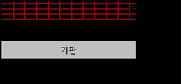
도 1 내지 4는 본 발명에 따른, 도전층(11), 성능 강화층(12), 반사방지막(21)을 포함하는 투명 전도성 막의 구조이다.
도 5는 표면처리 후, 필름의 절연 영역 (51) 및 도전 영역 (52)을 나타내는 사진이다.
도 6은 도 1의 구조를 갖는 투명전도성 필름의 과산화수소수로 표면처리한 후의 표면 사진이다.
도 7 및 8은 과염소산과 초산을 이용한 표면처리 후, 시인성 점수가 각각 1 및 2인 경우의 투명 전도성 필름의 현미경 사진이다.
1 to 4 are structures of a transparent conductive film including a conductive layer 11, a performance enhancement layer 12, and an antireflection film 21 according to the present invention.
5 is a photograph showing the insulating region 51 and the conductive region 52 of the film after the surface treatment.
Fig. 6 is a photograph of the surface of the transparent conductive film having the structure of Fig. 1 after surface treatment with hydrogen peroxide water.
FIGS. 7 and 8 are photomicrographs of a transparent conductive film with a visibility score of 1 and 2, respectively, after surface treatment with perchloric acid and acetic acid.
본 발명의 표면처리를 통한 금속 나노와이어 기반 투명 전도성 막의 패터닝 방법은 금속 나노와이어 기반의 투명 전도성 막의 패터닝 공정에 있어서, 1) 도전층 위에 성능 강화층을 추가하는 단계; 및 2) a) 과산화물 및 b) 유기산 또는 무기산을 포함하는 표면처리제 조성물을 이용하여 금속 나노와이어 투명 전도성 막을 표면 처리하는 단계를 포함하는 것을 특징으로 한다.
A method of patterning a metal nanowire-based transparent conductive film by surface treatment according to the present invention includes the steps of: 1) adding a performance enhancement layer on a conductive layer; And 2) surface treating the metal nanowire transparent conductive film using a surface treatment composition comprising a) a peroxide and b) an organic acid or an inorganic acid.
이하, 본 발명을 더욱 상세하게 설명한다.
Hereinafter, the present invention will be described in more detail.
1) 성능 강화층1) Performance enhancement layer
본 발명의 투명 전도성 막은 금속 나노와이어를 포함하는 도전성 층 위에 성능 강화를 위한 오버코팅 (Over-caoting) 소재를 올려 그 기능을 올릴 수 있으며, 성능 강화층 형성을 위한 조성물은 반사방지 특성을 가질 뿐만 아니라, 외부의 습기 및 온도 변화에 도전층을 보호할 수 있는 우수한 내구성 및 내환경성 특성을 부여하기 위하여 금속 산화물 졸을 포함할 수 있다. The transparent conductive film of the present invention can raise its function by placing an over-caoating material for enhancing performance on a conductive layer containing metal nanowires, and the composition for forming a performance enhancement layer has antireflection properties But may include a metal oxide sol to impart excellent durability and environmental resistance characteristics that can protect the conductive layer against external moisture and temperature changes.
본 발명의 일예로서, 도 1은 기판, 기판 위에 형성된 금속 나노와이어가 균일하게 도포되어 높은 전기 전도도를 나타낼 수 있도록 형성된 도전층(11), 및 그 위에 보호층 및 하드코팅 역할이 강조된 성능 강화층(12)을 포함하는 다중층 투명 전도성 막을 보여 준다.FIG. 1 is a cross-sectional view of a substrate according to an embodiment of the present invention. FIG. 1 is a cross-sectional view of a substrate, a conductive layer 11 formed on the substrate to uniformly coat the metal nanowires and exhibiting high electrical conductivity, Lt; RTI ID = 0.0 > (12). ≪ / RTI >
본 발명에서 사용가능한 금속 산화물 졸로는 불화 마그네슘 졸, 불화 칼슘 졸, ZTO(Zinc-Tin oxide) 졸, ZnO(Zinc Oxide)졸, 실리콘 옥사이드 졸, 주석 산화물 졸(Tin oxide), 망간 산화물 졸, 마그네슘 산화물 졸로 이루어진 군에서 선택되는 1종 이상의 금속 산화물 졸을 사용할 수 있으며, 조성물에서 금속산화물의 양은 바람직하기로 0.5 내지 5 중량%의 양으로 포함할 수 있다.Examples of the metal oxide sol usable in the present invention include magnesium fluoride sol, calcium fluoride sol, Zinc-Tin oxide sol, ZnO (Zinc Oxide) sol, silicon oxide sol, tin oxide, manganese oxide sol, And an oxide sol. The amount of the metal oxide in the composition is preferably in the range of 0.5 to 5% by weight.
또한 상기 성능 강화층 및 도전층의 저항 특성, 하드코팅 특성 등을 조절하기 위하여, 상기 금속 산화물 졸에 바인더를 추가로 첨가할 수 있으며, 구체적으로, 상기 바인더 수지는 금속산화물 졸과 섞였을 때 우수한 코팅성 및 막에 유연성을 부여하여 투명 도전성 막을 휘었을 때 깨지는 현상을 방지 할 수 있다.Further, a binder may be further added to the metal oxide sol in order to control the resistance characteristics, the hard coat properties, and the like of the performance enhancement layer and the conductive layer. Specifically, when the metal oxide sol is mixed with the metal oxide sol, It is possible to prevent the phenomenon of cracking when the transparent conductive film is warped by imparting coating property and flexibility to the film.
상기 금속 산화물 졸과 조합할 수 있는 바인더로는 셀룰로오스 수지, 폴리비닐알콜 수지, 폴리비닐부티랄 수지, 폴리우레탄 아크릴레이트 수지, 셀룰로오스 에테르 수지, 셀룰로오스 아세테이트 수지 등이 있으며, 이러한 바인더는 금속산화물 졸과 섞였을 때 우수한 코팅성 및 막에 유연성을 부여하여 투명 도전성 막을 휘었을 때 깨지는 현상을 방지 할 수 있다.Examples of the binder that can be combined with the metal oxide sol include a cellulose resin, a polyvinyl alcohol resin, a polyvinyl butyral resin, a polyurethane acrylate resin, a cellulose ether resin, and a cellulose acetate resin. It is possible to prevent the phenomenon of cracking when the transparent conductive film is warped by imparting excellent coating properties and flexibility to the film when mixed.
더욱 상세하게는, 상기 바인더는 하이드록시프로필메틸 셀룰로오스, 하이드록시에틸 셀룰로오스, 하이드록시프로필 셀룰로오스, 메틸 셀룰로오스, 에틸 셀룰로오스, 카르복시메틸 셀룰로오스, 트리아세틸 셀룰로오스, 디아세틸 셀룰로오스, 셀룰로오스 아세테이트 부트레이트, 셀룰로오스 아세테이트 프로피오네이트, 폴리비닐 알코올, 폴리비닐부티랄, 폴리비닐 피롤리돈, 폴리비닐부티랄비닐 알코올 코 폴리머, 폴리비닐 에스테르 말레익 코폴리머 등을 사용할 수 있다.More specifically, the binder is selected from the group consisting of hydroxypropylmethylcellulose, hydroxyethylcellulose, hydroxypropylcellulose, methylcellulose, ethylcellulose, carboxymethylcellulose, triacetylcellulose, diacetylcellulose, cellulose acetatebutrate, Polyvinyl alcohol, polyvinyl butyral, polyvinyl pyrrolidone, polyvinyl butyral vinyl alcohol copolymer, polyvinyl ester maleic copolymer, and the like can be used.
상기 바인더 수지는 본 발명의 성능 강화층 형성 조성물에 0.05 내지 10 중량%의 양으로 사용되는 것이 바람직하다. 상기 함량이 0.05 중량% 미만일 경우, 상기 유기 바인더 수지를 통해 점도 조절, 코팅성 향상, 기판과의 부착력 증가 및 유연성을 부여하기 위한 본래의 목적을 달성 할 수 없어 형성된 필름이 일정 이상 휘어질 경우 금속 나노와이어가 기판에서 이탈하거나, 전도성 코팅 조성물이 기판 전면에 균일하게 코팅이 되지 않아 전기전도성이 우수한 필름을 형성할 수 없는 우려가 있으며, 또한 상기 함량이 10 중량%를 초과하는 경우, 바인더 수지가 금속 나노와이어와 접촉을 저해하여 투명 전도성 막의 접촉 저항을 급격히 증가시키는 절연체 역할을 하게 되고, 점도가 급격히 상승하여 필름의 두께가 두껍게 형성되어 광학 특성을 악화시키는 문제가 발생할 수 있다. 필름 두께가 지나치게 두꺼워지면 필름 전체가 노란색을 띄게 되어 시인성에 악영향을 주게 된다. The binder resin is preferably used in an amount of 0.05 to 10% by weight in the performance-enhancing layer-forming composition of the present invention. When the content is less than 0.05% by weight, the organic binder resin can not achieve the original purpose of controlling the viscosity, improving the coating property, increasing the adhesion with the substrate and imparting flexibility, There is a fear that the nanowire may be detached from the substrate or the conductive coating composition may not be uniformly coated over the entire surface of the substrate and thus a film having excellent electrical conductivity may not be formed. When the content exceeds 10 wt%, the binder resin The metal nanowire is inhibited from contacting with the metal nanowire, thereby acting as an insulator which abruptly increases the contact resistance of the transparent conductive film, and the viscosity of the nanowire is rapidly increased to form a thick film, thereby deteriorating optical characteristics. If the thickness of the film becomes too thick, the entire film becomes yellow, which adversely affects visibility.
금속 산화물간의 조합 또는 금속 산화물과 바인더의 조합은 건조되면서 하부의 도전층에 포함되어 있는 금속 나노와이어 간의 밀착력을 증대시켜 금속 나노와이어의 접촉 저항을 낮출 수 있어 기존 도전층만 존재할 때 보다 낮은 저항을 구현 할 수 있는 저항 보강 효과를 나타낼 수 있으며, 더불어 넓은 면적에서의 저항 균일성이 개선되는 특성을 또한 나타낼 수 있다. A combination of metal oxides or a combination of a metal oxide and a binder may increase the adhesion between the metal nanowires included in the lower conductive layer and lower the contact resistance of the metal nanowire, It is possible to exhibit a resistance strengthening effect which can be implemented and also to exhibit the property that the resistance uniformity is improved in a wide area.
또한, 금속 산화물의 특성은 내구성 및 내 환경성에서 높은 신뢰성을 나타낼 수 있다. 즉, 투명 도전성 막의 물리적인 특성을 높일 수 있는 하드코팅(Hard coating) 역할을 하면서 경도 보강, 내마모성, 내환경성을 높일 수 있도록 하며, 표면처리를 위한 화학처리 공정에서 금속 나노와이어를 보호 할 수 있도록 한다. 이러한 특성은 금속 산화물 자체가 가스나 유체의 침투를 억제할 수 있는 역할을 하기 때문이다.In addition, the characteristics of the metal oxide can exhibit high reliability in durability and environmental resistance. In other words, it can serve as a hard coating that can enhance the physical properties of the transparent conductive film, while enhancing hardness reinforcement, abrasion resistance, and environmental resistance, and can protect the metal nanowire in the chemical treatment process for surface treatment do. This is because the metal oxide itself plays a role in suppressing gas or fluid penetration.
또한 본 발명의 투명 전도성 막은 반사방지막을 추가로 포함할 수 있다. 상기 반사방지막은 투명 도전체의 반사 표면에서의 반사 손실을 감소시킬 수 있는 층으로 표면처리 후 변하는 표면 광학 특성의 차이를 최소화 할 수 있는 기능을 한다. 상기 반사방지막은 공지의 반사방지막 형성용 조성물이 사용될 수 있음은 물론이며 일예로 MgF2 를 사용할 수 있다. 상기 반사방지막은 상기 보호층으로서의 성능 강화층의 상부, 상기 도전층의 하부 또는 기판의 배면에 형성될 수 있으며, 보호층의 상부에 형성될 경우, 우수한 시인성 보정효과를 얻을 수 있다.Further, the transparent conductive film of the present invention may further include an anti-reflection film. The antireflection film functions as a layer capable of reducing the reflection loss at the reflective surface of the transparent conductor so as to minimize the difference in the surface optical properties that change after the surface treatment. The antireflection film may be a known composition for forming an antireflection film. For example, MgF 2 may be used. The antireflection film may be formed on the upper part of the performance enhancement layer as the protective layer, the lower part of the conductive layer, or the backside of the substrate. When the antireflection film is formed on the protection layer, an excellent visibility correction effect can be obtained.
이와 같이 반사방지막은 반사방지 효과, 저항 보강 효과, 하드코팅 효과를 한꺼번에 수행 할 수 있는 복합 기능층으로써의 필요에 따라 도전층과 기판 사이 또는 도전층의 배면, 도전층 상부에 코팅 방식으로 형성될 수 있다.As described above, the antireflection film is formed as a composite functional layer capable of simultaneously performing the antireflection effect, the resistance reinforcing effect, and the hard coating effect on the back surface of the conductive layer or between the conductive layer and the substrate, .
본 발명의 투명 전도성 막은 도 2 내지 4에 나타난 구조를 가질 수 있다.The transparent conductive film of the present invention may have the structure shown in Figs.
도 2는 기판의 배면에 반사방지 기능이 강조된 반사방지막(21)을 추가로 포함하는 구조를 나타내며, 이때 상기 반사방지막(21)은 표면처리시 표면처리제에 의해 손상을 입지 않는 층으로 내 화학성이 뛰어난 막질이다.2 shows a structure further including an antireflection film 21 having an antireflection function emphasized on the backside of the substrate. In this case, the antireflection film 21 is a layer which is not damaged by the surface treatment agent during the surface treatment, Excellent membrane quality.
도 3은 보호층 및 하드코팅 역할을 하는 성능 강화층(12) 위에 반사방지막(21)을 추가로 포함하여 반사 방지 효과를 나타낼 수 있는 구조를 나타내며, 이에 따라 표면처리 후 색차에 의한 시인성을 보정해 줄 수 있다.FIG. 3 shows a structure capable of exhibiting an antireflection effect by further including an antireflection film 21 on a protective layer and a performance enhancement layer 12 serving as a hard coating, thereby correcting visibility due to color difference after surface treatment. You can do it.
도 4는 반사방지막(21) 위에 도전층(11)을 형성하고, 그 위에 보호층 및 하드코팅 역할이 강조된 성능 강화층(12)을 포함하는 구조를 나타낸다.
4 shows a structure in which a conductive layer 11 is formed on an antireflection film 21 and a performance enhancement layer 12 on which a protective layer and a hard coating function are emphasized.
상기 성능 강화층(12)과 반사방지막(21)은 통상의 방법에 따라 형성될 수 있으며, 예를 들어 슬릿 코팅, 바코팅, 스핀코팅 등의 방법을 이용하여 각각 10 내지 500 ㎚의 두께로 형성할 수 있다. 상기 층의 두께가 500 ㎚를 초과하는 경우, 저항 보강 효과가 없어지고 금속 나노와이어 자체의 면저항 특성을 저해시킬 수 있으며, 상기 두께가 10 ㎚ 미만일 경우, 성능 강화층으로서의 역할을 수행 할 수 없는 단점이 있다.
The performance enhancement layer 12 and the antireflection film 21 may be formed according to a conventional method and may be formed to a thickness of 10 to 500 nm using slit coating, bar coating, spin coating, can do. When the thickness of the layer is more than 500 nm, the resistance reinforcing effect is lost and the sheet resistance characteristic of the metal nanowire itself can be impaired. When the thickness is less than 10 nm, the layer can not serve as a performance enhancing layer .
22 ) 표면처리제 조성물) Surface treatment agent composition
본 발명에서는 상기와 같이 준비된 투명 도전층위에 먼저 DFR(Dry Film resist)을 올리고 광 패터닝 방법으로 DFR을 패터닝하여 준비한 후에 표면처리제를 선택된 영역에 접촉시켜 절연시키는 공정을 거치고 DFR을 제거함으로써 절연 영역과 도전 영역을 구분하는 패터닝 공정을 실시할 수 있다. 상기에서 표면처리제를 선택된 영역에 접촉시키는 방법은 스프레이코팅 또는 침지 등 공지의 방법이 적용될 수 있다. In the present invention, a DFR (dry film resist) is first formed on the transparent conductive layer prepared as described above, and the DFR is patterned by a photolithography method. Then, the surface treatment agent is contacted with a selected region to be insulated, A patterning process for separating conductive regions can be performed. A known method such as spray coating or immersion may be applied to the method of contacting the surface treatment agent to the selected area.
표면처리는 도전층에 포함된 금속 나노와이어의 표면 상태를 변화시켜 금속 염 화합물 또는 금속 산화물 형태로 변화시키는 공정으로 정의할 수 있으며, 일부 금속 염 화합물로 변화하는 과정에서 금속 나노와이어가 작은 단위로 끊어질 수 있다.The surface treatment can be defined as a process of changing the surface state of the metal nanowires included in the conductive layer to form a metal salt compound or a metal oxide. In the course of changing into a metal salt compound, It can be broken.
상기 표면 처리를 위해서는, a) 과산화물 및 b) 유기산 또는 무기산, 바람직하게는 a) 과염소산 또는 이의 염, 또는 과황산염, 및 b) 유기산이 포함된 표면처리제 조성물을 사용할 수 있다. 이러한 과염소산 계열의 화합물로는 차아염소산(Hypochlorite), 아염소산(Chlorite), 염소산(Chlorate), 과염소산(Perchlorate) 등이 있으며, 더욱 자세하게는 상기 과산화물은 과산화나트륨(Sodium peroxide), 카바마이드 퍼옥사이드(Carbamide peroxide), NaOCl, NaClO4, NaClO2, NaClO3, NH4ClO, NH4ClO2, NH4ClO3, NH4ClO4, KClO3, KClO, KClO4, KClO2 및 POCl3(Phosphorus oxychloride)이 사용될 수 있다. 상기 화합물은 약 0.1 내지 10 중량%의 양으로 증류수에 섞어서 사용할 수 있다.For the surface treatment, a surface treatment composition comprising a) a peroxide and b) an organic acid or an inorganic acid, preferably a) perchloric acid or a salt thereof or persulfate, and b) an organic acid may be used. Examples of such perchloric acid-based compounds include Hypochlorite, Chlorite, Chlorate and Perchlorate. More specifically, the peroxides include sodium peroxide, carbamide peroxide Carbamide peroxide), NaOCl, NaClO 4 , NaClO 2, NaClO 3, NH 4 ClO, NH 4 ClO 2, NH 4 ClO 3, NH 4 ClO 4, KClO 3, KClO, KClO 4, KClO 2 , and POCl 3 (Phosphorus oxychloride ) Can be used. The compound may be mixed with distilled water in an amount of about 0.1 to 10% by weight.
또한, 상기 과산화물 표면처리제는 무기 화합물 등과 더 혼합하여 사용할 수 있다.The peroxide surface treatment agent may be further mixed with an inorganic compound or the like.
상기 유기산, 무기산 또는 무기 화합물은 과산화물이 물과의 반응을 통해 계속 소모가 되기 때문에 좀 더 안정하게 과산화물이 표면처리제에 존재할 수 있도록 도움을 줄 수 있다. 이러한 유기산으로는 초산, 젖산, 말레익산, 숙신산, 옥살산, 말론산 등이 사용될 수 있으며, 무기산으로는 인산, 염산, 질산 등이 사용될 수 있고, 무기 화합물로는 구리, 철, 아연, 주석, 니켈의 염화물, 질화물, 아세테이트, 황화물 등을 사용할 수 있으며,약 0.1 내지 10 중량%로 과산화물과 함께 사용될 수 있다. 바람직하기로는 유기산인 것이 좋다.The organic acid, inorganic acid, or inorganic compound can help the peroxide to be present in the surface treatment agent more stably because the peroxide is continuously consumed through the reaction with water. Examples of the organic acid include acetic acid, lactic acid, maleic acid, succinic acid, oxalic acid and malonic acid. Examples of the inorganic acid include phosphoric acid, hydrochloric acid and nitric acid. Examples of the inorganic compound include copper, iron, zinc, tin and nickel Nitrates, acetates, sulfides, and the like, and may be used together with peroxide at about 0.1 to 10% by weight. Preferably, it is an organic acid.
상기 과산화물의 함량이 10 중량% 이상일 경우, 기능층에 손상을 주기 때문에 기능층으로써의 역할을 방해할 수 있으며, 0.1 중량% 미만일 경우, 금속 나노와이어를 산화시키지 못해 절연 영역을 만들지 못할 우려가 있다. 또한 상기 과산화물과 함께 적용 할 수 있는 유기산, 무기산 또는 무기 화합물이 10 중량%를 초과하는 경우 오히려 나노와이어를 단선시켜 시인성에 안 좋은 영향을 주기 때문에 기능층으로써의 역할을 방해할 수 있으며, 0.1 중량% 미만일 경우 과산화물과 함께 첨가하여 표면처리 효과를 높이거나 시간 단축 효과를 보일 수 없다. 즉, 과산화물을 안정화 시킬 수 없다.If the content of the peroxide is more than 10% by weight, the function layer may be damaged, which may hinder the function of the functional layer. If the content of the peroxide is less than 0.1% by weight, the metal nanowire may not be oxidized, . If the amount of the organic acid, inorganic acid, or inorganic compound that can be applied together with the peroxide is more than 10 wt%, the nanowire may be disconnection to adversely affect the visibility, %, It may be added together with the peroxide to increase the surface treatment effect or to shorten the time. That is, the peroxide can not be stabilized.
도 5는 본 발명에 따른 표면처리 조성물을 이용하여 표면 처리를 수행한 경우의 절연 영역(51)과 도전 영역(52)을 나타내고 있다. 상기 절연 영역과 도전 영역 모두에는 금속 나노와이어 구조가 그대로 나타나고 있으며, 도전 영역의 표면보다 절연 영역의 표면이 본래가지고 있던 밝기보다 좀 더 어두운 영역으로 나타나고 있다. 즉, 절연 영역에서는 금속 나노와이어 구조물이 끊어지거나 없어져 변경되지 않은 상태에서 금속 나노와이어의 표면 상태만 변경된 것을 알 수 있으며, 금속 나노와이어의 표면 상태가 변경됨으로써 절연효과를 가져올 수 있다.Fig. 5 shows the insulating region 51 and the conductive region 52 when the surface treatment is performed using the surface treatment composition according to the present invention. In both the insulating region and the conductive region, the metal nanowire structure appears as it is, and the surface of the insulating region appears to be darker than the inherent brightness of the surface of the conductive region. That is, in the insulating region, it can be seen that the surface state of the metal nanowire has been changed in a state where the metal nanowire structure is not broken or lost, and the surface state of the metal nanowire is changed, so that the insulating effect can be obtained.
구체적으로, 도 5의 금속 나노와이어로는 은을 적용하였으며, 이러한 경우, 은 나노와이어를 없애거나 짧게 끊어서 절연 상태로 만드는 기존의 방법보다 시인성에서 좀 더 우수한 특성을 나타낼 수 있다.Specifically, silver is applied to the metal nanowire of FIG. 5, and in this case, the nanowire can exhibit more excellent visibility than the conventional method of removing or shorting the nanowire into an insulating state.
따라서 본 발명에 따른 패터닝 방법은 비패턴부의 금속 나노와이어는 손상시키지 않으면서 절연성을 확보할 수 있는 것을 특징으로 한다. 절연 특성이 부여된 금속 나노와이어는 색상이 일부 변하거나 착색이 되는 현상을 보이기 때문에 일반 금속 나노와이어와 시인성에서 차이를 보일 수 있다. 그러나 본 발명에서는 표면 처리된 금속 나노와이어 층 위에 굴절률이 조절된 성능 강화층이 이러한 색상 차이에 의한 시인성을 극복할 수 있도록 하였다. 즉, 금속 나노와이어를 없애는 에칭공정 없이 절연 특성을 확보할 수 있는 공정을 도입하여 패턴부와 비패턴부의 헤이즈 차이를 최소화하는 것을 특징으로 한다.Therefore, the patterning method according to the present invention is characterized in that the insulating property can be ensured without damaging the metal nanowires of the non-pattern portion. Since the metal nanowires having the insulating characteristics exhibit some color change or coloration, they may show a difference in visibility with the general metal nanowires. However, in the present invention, the performance enhancement layer whose refractive index is controlled on the surface-treated metal nanowire layer can overcome the visibility due to such color difference. That is, a process capable of ensuring insulation characteristics without an etching process for removing metal nanowires is introduced to minimize the haze difference between the pattern portion and the non-pattern portion.
상기와 같이 표면처리된 영역에서의 표면 저항은 수 ㏁ 이상으로 절연 특성을 확보하여야 하며, 표면처리한 영역과 그렇지 않은 영역에서의 광학 특성 편차는 최소화 할 수 있도록 한다.
The surface resistance in the surface treated region as described above should have an insulation property of several MΩ or more, and optical characteristic deviations in the surface treated region and the non-treated region can be minimized.
3) 금속 나노와이어3) metal nanowires
본 발명의 전도성 코팅 조성물은 도전성 물질로서 금속 나노와이어를 사용한다. 본 발명에서 사용되는 금속 나노와이어는 통상적인 전도성 필름형성을 위하여 사용되는 금속 나노와이어가 사용될 수 있으며, 보다 구체적으로 사용 가능한 금속은 특별히 한정되지 않으나, 바람직하게는 금, 은, 구리, 알루미늄, 니켈, 주석, 팔라듐, 백금, 아연, 철, 인듐, 마그네슘 등의 Ⅰ족, ⅡA족, ⅢA족, ⅣA족 및 Ⅷ B족 금속으로 이루어진 군에서 선택되는 1종 이상의 금속을 사용하는 것이 좋으며, 더욱 바람직하게는 아연, 알루미늄, 주석, 구리, 은 및 금으로 이루어진 군에서 선택되는 1종 이상의 금속을 사용하는 것이 좋다. The conductive coating composition of the present invention uses metal nanowires as a conductive material. As the metal nanowires used in the present invention, metal nanowires used for forming a conventional conductive film may be used. More specifically, usable metals are not particularly limited, but gold, silver, copper, aluminum, nickel At least one metal selected from the group consisting of Group I, IIA, IIIA, IVA and VIII B metals such as tin, palladium, platinum, zinc, iron, indium and magnesium is preferably used It is preferable to use at least one metal selected from the group consisting of zinc, aluminum, tin, copper, silver and gold.
상기 금속 나노와이어는 직경이 15 nm 내지 120 nm, 길이가 5 ㎛ 내지 60 ㎛인 것이 바람직하다. The metal nanowires preferably have a diameter of 15 nm to 120 nm and a length of 5 to 60 탆.
본 발명에서 사용가능한 기판으로는 통상적으로 사용되는 투명 기판, 예를 들어, 폴리이미드(PI) 기판, 폴리에틸렌 테레프탈레이트(PET) 기판, 폴리카보네이트(PC) 기판, 싸이클로올레핀폴리머(COP) 기판, 폴리에틸렌나프탈레이트(PEN) 기판 등을 사용할 수 있다. Examples of the substrate that can be used in the present invention include transparent substrates commonly used such as a polyimide (PI) substrate, a polyethylene terephthalate (PET) substrate, a polycarbonate (PC) substrate, a cycloolefin polymer (COP) substrate, Naphthalate (PEN) substrate and the like can be used.
본 발명은 또한 상기 방법에 따라 형성된 투명 전도성 필름을 제공한다. 본 발명의 조성물 및 방법을 이용하여 제조된 투명 전도성 필름은 광투과도가 80% 이상이고, 면저항이 300 Ω/□ 이하이며, 면저항, 내환경성, 전투과도 및 헤이즈의 특성이 우수할 뿐 아니라, 에칭 공정 없이도 쉽게 표면처리가 가능하므로, 액정 표시장치, 플라즈마 표시장치, 터치패널, 전계발광 장치, 박막태양전지, 염료감응태양전지, 무기물 결정질 태양전지 등의 전극에 유용하게 활용될 수 있다.
The present invention also provides a transparent conductive film formed according to the above method. The transparent conductive film produced using the composition and method of the present invention has a light transmittance of 80% or more and a sheet resistance of 300 Ω / □ or less and is excellent in sheet resistance, environmental resistance, transient transient and haze characteristics, Since the surface can be easily processed without a process, it can be usefully applied to electrodes such as a liquid crystal display, a plasma display, a touch panel, an electroluminescent device, a thin film solar cell, a dye sensitized solar cell, and an inorganic crystalline solar cell.
이하, 본 발명의 이해를 돕기 위하여 바람직한 실시예를 제시하나, 하기 실시예는 본 발명을 예시하는 것일 뿐 본 발명의 범위가 하기 실시예에 한정되는 것은 아니다.
Hereinafter, the present invention will be described in more detail with reference to the following examples. However, the scope of the present invention is not limited to the following examples.
제조예 1Production Example 1 : 은 나노와이어를 포함하는 투명 전도성 막의 제조: Preparation of Transparent Conductive Films Containing Silver Nanowires
기판으로서는 광학적으로 투명한 절연체인 50 내지 188 ㎛ 두께의 폴리에틸렌테레프탈레이트(PET) 막을 사용하였다. 은 나노와이어(AgNW)는 폭이 약 20 nm 내지 70 nm이고 길이가 약 10 내지 30 ㎛인 것을 에탄올에 약 0.1 %w/v의 농도로 분산시켜 사용하였다. 점도 조절용 증점제로는 하이드록시프로필셀룰로오스(HPC, Hydroxypropyl cellulose)를 사용하였다. 상기 은 나노와이어 분산액을 기판 상에 침전(sediment)하도록 하여 바코터를 사용해 PET 기판 상에 코팅한 다음, 증발 건조하여 기판 및 도전층을 포함하는 투명 전도성 막을 제조하였다.
As the substrate, a polyethylene terephthalate (PET) film having a thickness of 50 to 188 m, which is an optically transparent insulator, was used. Silver nanowires (AgNW) were dispersed in ethanol at a concentration of about 0.1% w / v with a width of about 20 nm to 70 nm and a length of about 10 to 30 μm. Hydroxypropyl cellulose (HPC) was used as a thickener for viscosity control. The silver nanowire dispersion was sedimented on a substrate, coated on a PET substrate using a bar coater, and evaporated to dryness to prepare a transparent conductive film comprising a substrate and a conductive layer.
제조예 2Production Example 2 : 성능강화층의 형성: Formation of Performance Enhancement Layer
금속 산화물 졸로서 실리콘옥사이드 계열의 화합물을 12.5 %w/v의 농도로 에탄올에 분산시킨 다음, 여기에 0.5 %w/v 농도로 에탄올에 용해된 하이드록시프로필셀룰로오스를 바인더로서 2:1의 중량비로 혼합하고, 바코터를 사용해 상기 은 나노와이어를 포함하는 기판 상부에 보호층으로 코팅하고 증발건조하여, 기판 상부에 보호층으로서의 성능강화층을 형성하였다.
As a metal oxide sol, a compound of silicon oxide series was dispersed in ethanol at a concentration of 12.5% w / v, and hydroxypropylcellulose dissolved in ethanol at a concentration of 0.5% w / v was used as a binder at a weight ratio of 2: 1 Mixed and coated with a protective layer on top of the substrate containing the silver nanowires using a bar coater and evaporated to dryness to form a performance enhancement layer as a protective layer on the substrate.
제조예 3Production Example 3 : 도 2 내지 4의 구조를 갖는 투명 전도막의 제조: Preparation of a transparent conductive film having the structure shown in Figs. 2 to 4
상기 제조예 1 및 2의 조성물을 사용하고, 반사방지막 형성을 위하여 MgF2를 사용하여 도 2 내지 4의 구조를 갖는 투명 도전성 막을 제조하였다.
The transparent conductive films having the structures shown in Figs. 2 to 4 were prepared using the compositions of Production Examples 1 and 2 and MgF 2 for the formation of the antireflection film.
참고제조예 1Reference Example 1 : 투명 전도성 막의 제조: Preparation of transparent conductive film
은 나노와이어 분산액 대신에 은 나노와이어가 포함된 잉크를 사용한 것을 제외하고는 상기 실시예 1과 동일한 방법으로 기판을 제조한 다음, 상부 보호층으로서 실리콘옥사이드 계열 화합물을 0.15 %w/v의 농도로 초 순수에 녹인 용액을 바코터를 이용하여 은나노와이어 기판의 상부에 보호층으로 코팅하였다.
A substrate was prepared in the same manner as in Example 1, except that the ink containing silver nanowires was used instead of the nanowire dispersion. Then, a silicon oxide-based compound as an upper protective layer was coated at a concentration of 0.15% w / v The solution dissolved in the supernatant was coated with a protective layer on top of the silver nano wire substrate using a bar coater.
비교예 1-2Comparative Example 1-2
1 중량%의 과산화수소(H2O2)를 포함하는 표면처리제 1로는 상기 제조예 2의 투명 전도성 막을 표면처리하고, 1 중량% NaOCl 및 1 중량%의 KClO4를 포함하는 표면처리제 2로는 참고제조예의 투명 전도성 막을 각각 표면처리 하고, 시인성을 평가하였다.
As the surface treatment agent 1 containing 1% by weight of hydrogen peroxide (H 2 O 2 ), the surface of the transparent conductive film of Preparation Example 2 was surface-treated, and as the surface treatment agent 2 containing 1% by weight of NaOCl and 1% by weight of KClO 4 , Each of the transparent conductive films was subjected to surface treatment to evaluate visibility.
시인성 평가는 2명의 실험자가 각각 실험한 시편을 교차 평가하여 패턴이 완벽히 인식되지 않을 경우의 점수를 1로 하고 육안으로 완벽히 인식이 될 경우의 점수를 5로 하여 평가하였으며, 그 결과를 하기 표 1에 나타내었다.The visibility test was performed by crossing two test specimens, and the score of the case where the pattern was not completely recognized was set to 1, and the score of 5 when the pattern was completely recognized by the naked eye was evaluated. Respectively.
또한 도 1의 구조를 갖는 투명 전도성 막을 표면처리한 후의 표면 사진을 도 6에 나타내었다.Fig. 6 shows a surface photograph of the transparent conductive film having the structure shown in Fig. 1 after the surface treatment.
시간
(초)monorail
time
(second)
구조film
rescue
처리제surface
Treatment agent
1ingredient
One
%weight
%
2ingredient
2
%weight
%
3ingredient
3
%weight
%
1Reference example
One
도 6에 나타난 바와 같이 투명 전도성 막은 나노와이어가 완전히 제거되면서 개방회로가 되는 것을 확인하였으며, 상기 표 1에 나타난 바와 같이, 이러한 형태로 은 나노와이어가 제거될 경우 시인성 점수가 5임을 확인하였다. 이는 상부 성능강화층 또는 보호층이 과산화물을 충분히 막아주지 못하여 은 나노와이어를 제거되었기 때문에 시인성 좋지 않은 것으로 판단된다.
As shown in FIG. 6, it was confirmed that the transparent conductive film completely removed the nanowire and became an open circuit. As shown in Table 1, it was confirmed that the visibility score was 5 when the silver nanowire was removed in this form. This is because the upper performance enhancement layer or the protective layer does not sufficiently block the peroxide and thus the silver nanowire is removed, so that the visibility is not good.
실시예 1-8Examples 1-8
증류수에 희석한 과염소산, 및 과염소산의 안정화를 위해 초산을 2.5 중량%로 포함하는 조성물을 하기 표 2의 조성에 따라 제조한 다음, 각각 도 1 내지 4의 구조를 갖는 상기 제조예 2 내지 5의 투명 전도성 막에 처리하여 시인성을 평가하였으며, 그 결과를 하기 표 2에 나타내었다.To stabilize perchloric acid and perchloric acid diluted in distilled water, a composition containing 2.5% by weight of acetic acid was prepared according to the composition shown in the following Table 2, and then the transparent The conductive film was treated to evaluate visibility. The results are shown in Table 2 below.
시간
(초)monorail
time
(second)
구조film
rescue
처리제surface
Treatment agent
1ingredient
One
%weight
%
2ingredient
2
%weight
%
3ingredient
3
%weight
%
4ingredient
4
%weight
%
상기 표 2에 나타난 바와 같이, a) 과산화물 및 b) 유기산 또는 무기산을 포함하는 표면처리제 조성물을 이용하면, 은 나노와이어를 제거하지 않고도 패터닝을 진행할 수 있으며, 시인성이 1 또는 2(도 7 및 8 참조)로서 우수한 시인성을 확보할 수 있음을 알 수 있다. 특히, 도 3 구조의 경우에 더욱 우수한 시인성(시인성 1, 도 7)을 갖는 패턴닝을 진행할 수 있음을 확인하였다.As shown in Table 2, using a surface treatment composition comprising a) peroxide and b) an organic acid or inorganic acid, patterning can be performed without removing silver nanowires, and visibility is 1 or 2 (Figs. 7 and 8 (See, for example, US Pat. Particularly, it was confirmed that patterning with more excellent visibility (visibility 1, Fig. 7) can be proceeded in the case of the structure of Fig. 3.
Claims (15)
1) 도전층 위에 성능 강화층을 추가하는 단계; 및
2) a) 과산화물 및 b) 유기산 또는 무기산을 포함하는 표면처리제 조성물을 이용하여 금속 나노와이어 투명 전도성 막을 표면 처리하는 단계
를 포함하는 것을 특징으로 하는 표면처리를 통한 금속 나노와이어 기반 투명 전도성 막의 패터닝 방법.In the process of patterning a metal nanowire-based transparent conductive film,
1) adding a performance enhancement layer over the conductive layer; And
2) surface-treating the metal nanowire transparent conductive film using a surface treatment composition comprising a) a peroxide and b) an organic acid or an inorganic acid
And patterning the transparent conductive film based on the metal nanowire through the surface treatment.
상기 과산화물이 과산화나트륨(Sodium peroxide), 카바마이드 퍼옥사이드(Carbamide peroxide), NaOCl, NaClO4, NaClO2, NaClO3, NH4ClO, NH4ClO2, NH4ClO3, NH4ClO4, KClO3, KClO, KClO4, KClO2 및 POCl3(Phosphorus oxychloride)으로 이루어진 군에서 1종 이상 선택되는 것을 특징으로 하는 표면처리를 통한 금속 나노와이어 기반 투명 전도성 막의 패터닝 방법.The method according to claim 1,
Wherein the peroxide is sodium peroxide (Sodium peroxide), carbamide peroxide (Carbamide peroxide), NaOCl, NaClO 4, NaClO 2, NaClO 3, NH 4 ClO, NH 4 ClO 2, NH 4 ClO 3, NH 4 ClO 4, KClO 3 , KClO 4 , KClO 4 , KClO 2 and POCl 3 (Phosphorus oxychloride). The method for patterning a transparent conductive film based on metal nanowires by surface treatment is characterized in that
상기 과산화물이 0.1 내지 10 중량%의 양으로 표면처리제에 포함되는 것을 특징으로 하는 표면처리를 통한 금속 나노와이어 기반 투명 전도성 막의 패터닝 방법.The method according to claim 1,
Wherein the peroxide is included in the surface treatment agent in an amount of 0.1 to 10 wt%.
상기 유기산이 초산, 젖산, 말레인산, 숙신산, 옥살산 및 말론산으로 이루어진 군으로부터 1종 이상 선택되는 것을 특징으로 하는 표면처리를 통한 금속 나노와이어 기반 투명 전도성 막의 패터닝 방법.The method according to claim 1,
Wherein the organic acid is at least one selected from the group consisting of acetic acid, lactic acid, maleic acid, succinic acid, oxalic acid and malonic acid.
상기 무기산이 인산, 염산 및 질산으로 이루어진 군으로부터 1종 이상 선택되는 것을 특징으로 하는 표면처리를 통한 금속 나노와이어 기반 투명 전도성 막의 패터닝 방법.The method according to claim 1,
Wherein the inorganic acid is at least one selected from the group consisting of phosphoric acid, hydrochloric acid, and nitric acid, and a method of patterning the transparent conductive film based on the metal nanowire by surface treatment.
상기 표면처리제 조성물이 무기 화합물을 추가로 포함하는 것을 특징으로 하는 표면처리를 통한 금속 나노와이어 기반 투명 전도성 막의 패터닝 방법.The method according to claim 1,
Wherein the surface treatment agent composition further comprises an inorganic compound. ≪ RTI ID = 0.0 > 11. < / RTI >
상기 유기산 또는 무기산이 표면처리제에 0.1 내지 10 중량%의 양으로 포함되는 것을 특징으로 하는 표면처리를 통한 금속 나노와이어 기반 투명 전도성 막의 패터닝 방법.The method according to claim 1,
Wherein the organic acid or inorganic acid is contained in the surface treating agent in an amount of 0.1 to 10% by weight based on the total weight of the transparent conductive film.
상기 성능 강화층이 금속 산화물 졸을 포함하는 조성물로 형성된 것을 특징으로 하는 표면처리를 통한 금속 나노와이어 기반 투명 전도성 막의 패터닝 방법.The method according to claim 1,
Wherein the performance enhancing layer is formed of a composition comprising a metal oxide sol. ≪ RTI ID = 0.0 > 11. < / RTI >
상기 금속 산화물 졸이 불화 마그네슘 졸, 불화 칼슘 졸, ZTO(Zinc-Tin oxide) 졸, ZnO(Zinc Oxide)졸, 실리콘 옥사이드 졸, 주석 산화물 졸(Tin oxide), 망간 산화물 졸, 마그네슘 산화물 졸로 이루어진 군에서 선택되는 1종 이상의 금속 산화물 졸인 것을 특징으로 하는 표면처리를 통한 금속 나노와이어 기반 투명 전도성 막의 패터닝 방법.9. The method of claim 8,
Wherein the metal oxide sol is selected from the group consisting of magnesium fluoride sol, calcium fluoride sol, Zinc-Tin oxide sol, ZnO (Zinc Oxide) sol, silicon oxide sol, tin oxide, manganese oxide sol, Wherein at least one of the metal oxide nanoparticles is a metal oxide nanoparticle.
상기 조성물이 바인더를 추가로 포함하는 것을 특징으로 하는 표면처리를 통한 금속 나노와이어 기반 투명 전도성 막의 패터닝 방법.9. The method of claim 8,
Wherein the composition further comprises a binder. ≪ RTI ID = 0.0 > 8. < / RTI >
상기 바인더가 셀룰로오스 수지, 폴리비닐알콜 수지, 폴리비닐부티랄 수지, 폴리우레탄 아크릴레이트 수지, 셀룰로오스 에테르 수지 및 셀룰로오스 아세테이트 수지로 이루어진 군으로부터 1종 이상 선택되는 것을 특징으로 하는 표면처리를 통한 금속 나노와이어 기반 투명 전도성 막의 패터닝 방법.11. The method of claim 10,
Wherein the binder is at least one selected from the group consisting of a cellulose resin, a polyvinyl alcohol resin, a polyvinyl butyral resin, a polyurethane acrylate resin, a cellulose ether resin and a cellulose acetate resin. Based transparent conductive film.
상기 금속 나노와이어는 직경이 15 nm 내지 120 nm이고, 길이가 5 ㎛ 내지 60 ㎛인 것 특징으로 하는 표면처리를 통한 금속 나노와이어 기반 투명 전도성 막의 패터닝 방법.The method according to claim 1,
Wherein the metal nanowire has a diameter of 15 nm to 120 nm and a length of 5 to 60 탆.
상기 투명 전도성 막의 투과율은 적어도 80%이고, 면저항이 300 Ω/□ 이하인 것을 특징으로 하는 투명 전도성 막.14. The method of claim 13,
Wherein the transparent conductive film has a transmittance of at least 80% and a sheet resistance of 300 Ω / □ or less.
Priority Applications (5)
| Application Number | Priority Date | Filing Date | Title |
|---|---|---|---|
| KR1020130166586A KR20150077765A (en) | 2013-12-30 | 2013-12-30 | Method for pattering metallic nanowire-based transparent conductive film by surface treatment |
| CN201480071451.2A CN105900188B (en) | 2013-12-30 | 2014-12-29 | Patterning method of metal nanowire-based transparent conductive film by surface treatment |
| JP2016541601A JP6633525B2 (en) | 2013-12-30 | 2014-12-29 | Method of patterning metal nanowire-based transparent conductive film through surface treatment |
| US15/101,488 US10410758B2 (en) | 2013-12-30 | 2014-12-29 | Method for patterning metal nanowire-based transparent conductive film through surface treatment |
| PCT/KR2014/012964 WO2015102335A1 (en) | 2013-12-30 | 2014-12-29 | Method for patterning metal nanowire-based transparent conductive film through surface treatment |
Applications Claiming Priority (1)
| Application Number | Priority Date | Filing Date | Title |
|---|---|---|---|
| KR1020130166586A KR20150077765A (en) | 2013-12-30 | 2013-12-30 | Method for pattering metallic nanowire-based transparent conductive film by surface treatment |
Publications (1)
| Publication Number | Publication Date |
|---|---|
| KR20150077765A true KR20150077765A (en) | 2015-07-08 |
Family
ID=53493624
Family Applications (1)
| Application Number | Title | Priority Date | Filing Date |
|---|---|---|---|
| KR1020130166586A Ceased KR20150077765A (en) | 2013-12-30 | 2013-12-30 | Method for pattering metallic nanowire-based transparent conductive film by surface treatment |
Country Status (5)
| Country | Link |
|---|---|
| US (1) | US10410758B2 (en) |
| JP (1) | JP6633525B2 (en) |
| KR (1) | KR20150077765A (en) |
| CN (1) | CN105900188B (en) |
| WO (1) | WO2015102335A1 (en) |
Cited By (1)
| Publication number | Priority date | Publication date | Assignee | Title |
|---|---|---|---|---|
| KR20230085798A (en) * | 2021-12-07 | 2023-06-14 | 국민대학교산학협력단 | Method for Preparing Supercapacitor Electrode by Using Nanoparticles with Improved Dispersibility, Electrode Prepared Thereby and Transparent Supercapacitor Using Same |
Families Citing this family (4)
| Publication number | Priority date | Publication date | Assignee | Title |
|---|---|---|---|---|
| KR20170141663A (en) * | 2015-04-16 | 2017-12-26 | 바스프 에스이 | Patterned transparent conductive film and process for producing such a patterned transparent conductive film |
| FI20155713A (en) * | 2015-10-09 | 2017-04-10 | Inkron Ltd | Electrically conductive siloxane particle films and devices containing the same |
| CN106356298A (en) * | 2016-09-18 | 2017-01-25 | 昆山工研院新型平板显示技术中心有限公司 | Preparation method for silver nanowire film pattern and display substrate and display device |
| CN112154175B (en) * | 2018-05-18 | 2023-01-17 | 国立大学法人大阪大学 | Method for producing surface-treated polymer, polymer, metal-coated polymer, and adhesive laminate, and methods for producing them |
Family Cites Families (8)
| Publication number | Priority date | Publication date | Assignee | Title |
|---|---|---|---|---|
| EP1965438A3 (en) * | 2005-08-12 | 2009-05-13 | Cambrios Technologies Corporation | Nanowires-based transparent conductors |
| JP5409369B2 (en) * | 2006-10-12 | 2014-02-05 | カンブリオス テクノロジーズ コーポレイション | Nanowire-based transparent conductor and its application |
| US20120180852A1 (en) * | 2011-01-13 | 2012-07-19 | E.I. Du Pont De Nemours And Company | Etching composition |
| KR20120134955A (en) | 2011-06-03 | 2012-12-12 | (주)네패스디스플레이 | Touch panel having improved visibility and method for manufacturing the same |
| KR101359913B1 (en) * | 2011-12-07 | 2014-02-11 | (주)솔라세라믹 | The manufacturing method of low-resistance, high transmittance, flexible FTO(F-doped Tin Oxide) transparent conductive film including carbon nanotubes |
| CN102543303B (en) * | 2011-12-16 | 2013-12-11 | 苏州汉纳材料科技有限公司 | Patterned transparent electrode fabrication method |
| JP5749207B2 (en) * | 2012-03-23 | 2015-07-15 | 富士フイルム株式会社 | Transparent conductive film laminate and touch panel |
| JP5865851B2 (en) * | 2012-03-23 | 2016-02-17 | 富士フイルム株式会社 | Manufacturing method of conductive member, conductive member, and touch panel using the same |
-
2013
- 2013-12-30 KR KR1020130166586A patent/KR20150077765A/en not_active Ceased
-
2014
- 2014-12-29 US US15/101,488 patent/US10410758B2/en not_active Expired - Fee Related
- 2014-12-29 WO PCT/KR2014/012964 patent/WO2015102335A1/en not_active Ceased
- 2014-12-29 CN CN201480071451.2A patent/CN105900188B/en not_active Expired - Fee Related
- 2014-12-29 JP JP2016541601A patent/JP6633525B2/en not_active Expired - Fee Related
Cited By (1)
| Publication number | Priority date | Publication date | Assignee | Title |
|---|---|---|---|---|
| KR20230085798A (en) * | 2021-12-07 | 2023-06-14 | 국민대학교산학협력단 | Method for Preparing Supercapacitor Electrode by Using Nanoparticles with Improved Dispersibility, Electrode Prepared Thereby and Transparent Supercapacitor Using Same |
Also Published As
| Publication number | Publication date |
|---|---|
| US10410758B2 (en) | 2019-09-10 |
| CN105900188B (en) | 2019-12-17 |
| JP6633525B2 (en) | 2020-01-22 |
| WO2015102335A1 (en) | 2015-07-09 |
| US20180174703A1 (en) | 2018-06-21 |
| CN105900188A (en) | 2016-08-24 |
| JP2017514264A (en) | 2017-06-01 |
Similar Documents
| Publication | Publication Date | Title |
|---|---|---|
| KR100272820B1 (en) | Transparent electrically conductive film-attached substrate and display element using it | |
| US9023217B2 (en) | Etch patterning of nanostructure transparent conductors | |
| KR101946653B1 (en) | Transparent conductive film | |
| TWI570600B (en) | Transparent conductor and touch panel | |
| KR20150077765A (en) | Method for pattering metallic nanowire-based transparent conductive film by surface treatment | |
| CN107210092B (en) | Substrate with conductive layer, substrate with transparent electrode for touch panel, and their manufacturing method | |
| KR20130026921A (en) | Transparent conductive film, method for making the same and touch panel with it | |
| KR102522012B1 (en) | Conductive element and electronic devices comprising the same | |
| JP6632694B2 (en) | Transparent conductor and process for fabricating the transparent conductor | |
| WO2017099187A1 (en) | Transparent conductor | |
| KR20160035998A (en) | Conductive structure body and method for manufacturing the same | |
| WO1998004406A1 (en) | Transparent conductive film and method for forming transparent electrode | |
| KR20170067204A (en) | Manufacturing method of metal nanowire electrode | |
| EP3471111A1 (en) | Transparent conductor | |
| KR20160020230A (en) | Manufacturing method of transparent electrod and transparent electrod laminate | |
| KR101756260B1 (en) | Touch sensor laminate comprising silver nanowire conductive layer and manufacturing methods of thereof | |
| KR20200114559A (en) | Touch panel including silver nanowire touch sensor and manufacturing method thereof | |
| KR20140084392A (en) | A transparency conductive board and Method of manufacturing thereof | |
| CN203759661U (en) | Touch panel with optical matching layer structure | |
| KR20190063990A (en) | Transparent conductive films and manufacturing method thereof | |
| CN102157223A (en) | Transparent conductive laminate and method for producing same | |
| CN111883287A (en) | Low-sheet-resistance transparent conductive film | |
| KR101535208B1 (en) | Transparent conductive film having metal nano-wire structure | |
| KR20150024751A (en) | Silver & silver alloy etchant for metal electrode & reflection layer | |
| KR101840938B1 (en) | Method for transparent electrode with improved work function |
Legal Events
| Date | Code | Title | Description |
|---|---|---|---|
| PA0109 | Patent application |
Patent event code: PA01091R01D Comment text: Patent Application Patent event date: 20131230 |
|
| PG1501 | Laying open of application | ||
| A201 | Request for examination | ||
| PA0201 | Request for examination |
Patent event code: PA02012R01D Patent event date: 20181224 Comment text: Request for Examination of Application Patent event code: PA02011R01I Patent event date: 20131230 Comment text: Patent Application |
|
| E902 | Notification of reason for refusal | ||
| PE0902 | Notice of grounds for rejection |
Comment text: Notification of reason for refusal Patent event date: 20200206 Patent event code: PE09021S01D |
|
| E601 | Decision to refuse application | ||
| PE0601 | Decision on rejection of patent |
Patent event date: 20200701 Comment text: Decision to Refuse Application Patent event code: PE06012S01D Patent event date: 20200206 Comment text: Notification of reason for refusal Patent event code: PE06011S01I |