KR20150033614A - Illumination apparatus, processing apparatus, and method for manufacturing device - Google Patents
Illumination apparatus, processing apparatus, and method for manufacturing device Download PDFInfo
- Publication number
- KR20150033614A KR20150033614A KR20147035788A KR20147035788A KR20150033614A KR 20150033614 A KR20150033614 A KR 20150033614A KR 20147035788 A KR20147035788 A KR 20147035788A KR 20147035788 A KR20147035788 A KR 20147035788A KR 20150033614 A KR20150033614 A KR 20150033614A
- Authority
- KR
- South Korea
- Prior art keywords
- light
- optical system
- integrator
- light source
- illumination
- Prior art date
- Legal status (The legal status is an assumption and is not a legal conclusion. Google has not performed a legal analysis and makes no representation as to the accuracy of the status listed.)
- Withdrawn
Links
- 238000005286 illumination Methods 0.000 title claims description 278
- 238000012545 processing Methods 0.000 title claims description 47
- 238000000034 method Methods 0.000 title claims description 37
- 238000004519 manufacturing process Methods 0.000 title description 24
- 230000003287 optical effect Effects 0.000 claims abstract description 324
- 239000000758 substrate Substances 0.000 claims description 103
- 238000009826 distribution Methods 0.000 claims description 61
- 239000013307 optical fiber Substances 0.000 claims description 59
- 238000003384 imaging method Methods 0.000 claims description 52
- 230000004907 flux Effects 0.000 claims description 41
- 230000007480 spreading Effects 0.000 claims description 29
- 238000003892 spreading Methods 0.000 claims description 29
- 239000007787 solid Substances 0.000 claims description 15
- 230000008859 change Effects 0.000 claims description 3
- 239000011295 pitch Substances 0.000 description 28
- 239000010408 film Substances 0.000 description 14
- 239000010410 layer Substances 0.000 description 10
- 230000008569 process Effects 0.000 description 10
- 229920005989 resin Polymers 0.000 description 10
- 239000011347 resin Substances 0.000 description 10
- 238000006243 chemical reaction Methods 0.000 description 8
- 238000001514 detection method Methods 0.000 description 8
- 239000011521 glass Substances 0.000 description 7
- VYPSYNLAJGMNEJ-UHFFFAOYSA-N silicon dioxide Inorganic materials O=[Si]=O VYPSYNLAJGMNEJ-UHFFFAOYSA-N 0.000 description 6
- 238000006073 displacement reaction Methods 0.000 description 5
- 239000000463 material Substances 0.000 description 5
- 239000010453 quartz Substances 0.000 description 5
- 238000012546 transfer Methods 0.000 description 5
- 238000010586 diagram Methods 0.000 description 4
- 239000011888 foil Substances 0.000 description 4
- 238000000137 annealing Methods 0.000 description 3
- 238000000576 coating method Methods 0.000 description 3
- 239000002346 layers by function Substances 0.000 description 3
- 239000007788 liquid Substances 0.000 description 3
- 239000004973 liquid crystal related substance Substances 0.000 description 3
- 230000002093 peripheral effect Effects 0.000 description 3
- XLOMVQKBTHCTTD-UHFFFAOYSA-N Zinc monoxide Chemical compound [Zn]=O XLOMVQKBTHCTTD-UHFFFAOYSA-N 0.000 description 2
- 239000011248 coating agent Substances 0.000 description 2
- 238000012937 correction Methods 0.000 description 2
- 230000008878 coupling Effects 0.000 description 2
- 238000010168 coupling process Methods 0.000 description 2
- 238000005859 coupling reaction Methods 0.000 description 2
- 238000005530 etching Methods 0.000 description 2
- 238000010438 heat treatment Methods 0.000 description 2
- 239000011256 inorganic filler Substances 0.000 description 2
- 229910003475 inorganic filler Inorganic materials 0.000 description 2
- 238000007689 inspection Methods 0.000 description 2
- 229910052751 metal Inorganic materials 0.000 description 2
- 239000002184 metal Substances 0.000 description 2
- 239000004065 semiconductor Substances 0.000 description 2
- 238000004088 simulation Methods 0.000 description 2
- 238000011282 treatment Methods 0.000 description 2
- 238000012935 Averaging Methods 0.000 description 1
- VYZAMTAEIAYCRO-UHFFFAOYSA-N Chromium Chemical compound [Cr] VYZAMTAEIAYCRO-UHFFFAOYSA-N 0.000 description 1
- VGGSQFUCUMXWEO-UHFFFAOYSA-N Ethene Chemical compound C=C VGGSQFUCUMXWEO-UHFFFAOYSA-N 0.000 description 1
- 239000005977 Ethylene Substances 0.000 description 1
- 238000006124 Pilkington process Methods 0.000 description 1
- 239000004743 Polypropylene Substances 0.000 description 1
- BLRPTPMANUNPDV-UHFFFAOYSA-N Silane Chemical compound [SiH4] BLRPTPMANUNPDV-UHFFFAOYSA-N 0.000 description 1
- GWEVSGVZZGPLCZ-UHFFFAOYSA-N Titan oxide Chemical compound O=[Ti]=O GWEVSGVZZGPLCZ-UHFFFAOYSA-N 0.000 description 1
- XTXRWKRVRITETP-UHFFFAOYSA-N Vinyl acetate Chemical compound CC(=O)OC=C XTXRWKRVRITETP-UHFFFAOYSA-N 0.000 description 1
- 230000009471 action Effects 0.000 description 1
- 230000003213 activating effect Effects 0.000 description 1
- 239000000853 adhesive Substances 0.000 description 1
- 230000001070 adhesive effect Effects 0.000 description 1
- 229910045601 alloy Inorganic materials 0.000 description 1
- 239000000956 alloy Substances 0.000 description 1
- PNEYBMLMFCGWSK-UHFFFAOYSA-N aluminium oxide Inorganic materials [O-2].[O-2].[O-2].[Al+3].[Al+3] PNEYBMLMFCGWSK-UHFFFAOYSA-N 0.000 description 1
- 238000005452 bending Methods 0.000 description 1
- 239000012461 cellulose resin Substances 0.000 description 1
- 229910052804 chromium Inorganic materials 0.000 description 1
- 239000011651 chromium Substances 0.000 description 1
- 238000002425 crystallisation Methods 0.000 description 1
- 230000008025 crystallization Effects 0.000 description 1
- 238000013461 design Methods 0.000 description 1
- 238000001035 drying Methods 0.000 description 1
- 238000007772 electroless plating Methods 0.000 description 1
- 230000006266 hibernation Effects 0.000 description 1
- 238000002347 injection Methods 0.000 description 1
- 239000007924 injection Substances 0.000 description 1
- 238000005259 measurement Methods 0.000 description 1
- 238000002156 mixing Methods 0.000 description 1
- 238000012544 monitoring process Methods 0.000 description 1
- 238000005192 partition Methods 0.000 description 1
- 238000000059 patterning Methods 0.000 description 1
- 229920002120 photoresistant polymer Polymers 0.000 description 1
- 238000007747 plating Methods 0.000 description 1
- 229920006122 polyamide resin Polymers 0.000 description 1
- 229920005668 polycarbonate resin Polymers 0.000 description 1
- 239000004431 polycarbonate resin Substances 0.000 description 1
- 229920001225 polyester resin Polymers 0.000 description 1
- 239000004645 polyester resin Substances 0.000 description 1
- 229920013716 polyethylene resin Polymers 0.000 description 1
- 229920001721 polyimide Polymers 0.000 description 1
- 239000009719 polyimide resin Substances 0.000 description 1
- -1 polypropylene Polymers 0.000 description 1
- 229920001155 polypropylene Polymers 0.000 description 1
- 229920005990 polystyrene resin Polymers 0.000 description 1
- 239000004800 polyvinyl chloride Substances 0.000 description 1
- 229920000915 polyvinyl chloride Polymers 0.000 description 1
- 238000012805 post-processing Methods 0.000 description 1
- 230000001376 precipitating effect Effects 0.000 description 1
- 238000007639 printing Methods 0.000 description 1
- 210000001747 pupil Anatomy 0.000 description 1
- ASAWWUJEMFFVLB-JPXADNNBSA-N pyx 2 Chemical compound C([C@@H](C(=O)N[C@@H]([C@@H](C)CC)C(=O)N[C@@H](CC(N)=O)C(=O)N[C@@H](CC(C)C)C(=O)N[C@@H]([C@@H](C)CC)C(=O)N[C@H]([C@H](C)O)C(=O)N[C@@H](CCCNC(N)=N)C(=O)N[C@@H](CCC(N)=O)C(=O)N[C@@H](CCCNC(N)=N)C(=O)NC(=O)[C@@H](N)CC=1C=C(CC=2C(=CC=CC=2Cl)Cl)C(O)=CC=1)NC(C)=O)C(C=1)=CC=C(O)C=1CC1=C(Cl)C=CC=C1Cl ASAWWUJEMFFVLB-JPXADNNBSA-N 0.000 description 1
- 238000011084 recovery Methods 0.000 description 1
- 230000002940 repellent Effects 0.000 description 1
- 239000005871 repellent Substances 0.000 description 1
- 238000007789 sealing Methods 0.000 description 1
- 229910000077 silane Inorganic materials 0.000 description 1
- 229910052814 silicon oxide Inorganic materials 0.000 description 1
- 239000002356 single layer Substances 0.000 description 1
- 239000010935 stainless steel Substances 0.000 description 1
- 229910001220 stainless steel Inorganic materials 0.000 description 1
- 239000010409 thin film Substances 0.000 description 1
- OGIDPMRJRNCKJF-UHFFFAOYSA-N titanium oxide Inorganic materials [Ti]=O OGIDPMRJRNCKJF-UHFFFAOYSA-N 0.000 description 1
- 238000002834 transmittance Methods 0.000 description 1
- 229920006163 vinyl copolymer Polymers 0.000 description 1
- 230000000007 visual effect Effects 0.000 description 1
- XLYOFNOQVPJJNP-UHFFFAOYSA-N water Substances O XLYOFNOQVPJJNP-UHFFFAOYSA-N 0.000 description 1
- 238000004804 winding Methods 0.000 description 1
- 239000011787 zinc oxide Substances 0.000 description 1
Images


Classifications
-
- G—PHYSICS
- G03—PHOTOGRAPHY; CINEMATOGRAPHY; ANALOGOUS TECHNIQUES USING WAVES OTHER THAN OPTICAL WAVES; ELECTROGRAPHY; HOLOGRAPHY
- G03F—PHOTOMECHANICAL PRODUCTION OF TEXTURED OR PATTERNED SURFACES, e.g. FOR PRINTING, FOR PROCESSING OF SEMICONDUCTOR DEVICES; MATERIALS THEREFOR; ORIGINALS THEREFOR; APPARATUS SPECIALLY ADAPTED THEREFOR
- G03F7/00—Photomechanical, e.g. photolithographic, production of textured or patterned surfaces, e.g. printing surfaces; Materials therefor, e.g. comprising photoresists; Apparatus specially adapted therefor
- G03F7/20—Exposure; Apparatus therefor
-
- G—PHYSICS
- G03—PHOTOGRAPHY; CINEMATOGRAPHY; ANALOGOUS TECHNIQUES USING WAVES OTHER THAN OPTICAL WAVES; ELECTROGRAPHY; HOLOGRAPHY
- G03F—PHOTOMECHANICAL PRODUCTION OF TEXTURED OR PATTERNED SURFACES, e.g. FOR PRINTING, FOR PROCESSING OF SEMICONDUCTOR DEVICES; MATERIALS THEREFOR; ORIGINALS THEREFOR; APPARATUS SPECIALLY ADAPTED THEREFOR
- G03F7/00—Photomechanical, e.g. photolithographic, production of textured or patterned surfaces, e.g. printing surfaces; Materials therefor, e.g. comprising photoresists; Apparatus specially adapted therefor
- G03F7/70—Microphotolithographic exposure; Apparatus therefor
- G03F7/70058—Mask illumination systems
- G03F7/70075—Homogenization of illumination intensity in the mask plane by using an integrator, e.g. fly's eye lens, facet mirror or glass rod, by using a diffusing optical element or by beam deflection
-
- G—PHYSICS
- G03—PHOTOGRAPHY; CINEMATOGRAPHY; ANALOGOUS TECHNIQUES USING WAVES OTHER THAN OPTICAL WAVES; ELECTROGRAPHY; HOLOGRAPHY
- G03F—PHOTOMECHANICAL PRODUCTION OF TEXTURED OR PATTERNED SURFACES, e.g. FOR PRINTING, FOR PROCESSING OF SEMICONDUCTOR DEVICES; MATERIALS THEREFOR; ORIGINALS THEREFOR; APPARATUS SPECIALLY ADAPTED THEREFOR
- G03F7/00—Photomechanical, e.g. photolithographic, production of textured or patterned surfaces, e.g. printing surfaces; Materials therefor, e.g. comprising photoresists; Apparatus specially adapted therefor
- G03F7/70—Microphotolithographic exposure; Apparatus therefor
- G03F7/70008—Production of exposure light, i.e. light sources
Landscapes
- Physics & Mathematics (AREA)
- General Physics & Mathematics (AREA)
- Exposure And Positioning Against Photoresist Photosensitive Materials (AREA)
- Exposure Of Semiconductors, Excluding Electron Or Ion Beam Exposure (AREA)
- Microscoopes, Condenser (AREA)
Abstract
조명 장치는, 장방형의 제1 면, 내면, 및 장방형의 제2 면을 가지며, 상기 제1 면에 입사한 광이 상기 내면에서의 다중 반사를 통해서 상기 제2 면으로부터 출사하는 광 인티그레이터와, 광원으로부터의 광을 상기 광 인티그레이터로 안내하는 도광부이며, 상기 제1 면의 긴 길이 방향을 따라서 소정의 간격으로 늘어서는 복수의 광속을 상기 광 인티그레이터에 공급하는 상기 도광부와, 상기 제2 면의 짧은 길이 방향에 관하여 상기 제2 면과 공역인 공역면을 형성하며, 상기 제2 면의 짧은 길이 방향에 관한 굴절력에 비해 상기 제2 면의 긴 길이 방향에 관한 굴절력이 작은 결상 광학계를 구비한다. A light integrator having a rectangular first surface, an inner surface, and a second rectangular surface, wherein light incident on the first surface is emitted from the second surface through multiple reflections on the inner surface; A light guide portion for guiding light from a light source to the optical integrator, the light guide portion supplying a plurality of light beams lined up at a predetermined interval along a long longitudinal direction of the first surface to the optical integrator; Wherein the second surface is formed with a conjugate plane which is conjugate with the second surface with respect to the short-length direction of the two surfaces, and the second surface has a smaller refractive power with respect to the long- Respectively.
Description
본 발명은, 조명 장치, 처리 장치, 및 디바이스 제조 방법에 관한 것이다.The present invention relates to a lighting device, a processing device, and a device manufacturing method.
본원은, 2012년 6월 21일의 미국 가출원 61/662,571호에 기초하여 우선권을 주장하고, 그 내용을 여기에 원용한다. The present application claims priority based on U.S. Provisional Application No. 61 / 662,571, filed on June 21, 2012, the contents of which are incorporated herein by reference.
최근, 텔레비전 등의 표시장치로서, 예를 들면 유기 EL 표시 패널, 액정 표시 패널 등의 디바이스가 많이 이용되고 있다. 이러한 각종의 디바이스는, 예를 들면, 노광(露光) 처리 및 에칭 기술을 이용하여, 유리 플레이트 등의 기판 상에 투명 박막 전극 등의 각종의 막패턴을 형성하는 것에 의해서 제조된다. 디바이스를 제조하는 형태의 하나로서, 필름 모양의 기판을 반송하면서, 반송 경로 상에서 기판에 노광 처리 등의 각종 처리를 행하는 롤·투·롤 방식의 제조 방법이 제안되어 있다(예를 들면, 특허 문헌 1 참조). 2. Description of the Related Art In recent years, devices such as organic EL display panels and liquid crystal display panels have been widely used as display devices for televisions and the like. Such various devices are manufactured by forming various film patterns such as transparent thin film electrodes on a substrate such as a glass plate by using, for example, an exposure process and an etching technique. As a form of manufacturing a device, there has been proposed a roll-to-roll type manufacturing method in which a film-like substrate is transported and various treatments such as exposure treatment are performed on the substrate on a transport path (see, for example, 1).
노광 장치 등의 처리 장치는, 효율 좋게 디바이스를 제조 가능하게 하는 등의 관점에서, 처리 범위를 넓히는 것이 기대된다. 이러한 처리 장치에 이용되는 조명 장치는, 피처리물의 이동 방향에 수직인 방향의 광의 조사 범위를 넓히는 것이 기대된다. A processing apparatus such as an exposure apparatus is expected to widen the processing range from the viewpoint of enabling the device to be produced efficiently. It is expected that the illuminating device used in such a processing apparatus widen the irradiation range of the light in the direction perpendicular to the moving direction of the object to be processed.
본 발명에 관한 형태는, 처리 범위를 넓히는 것을 가능하게 하는 조명 장치, 처리 장치, 및 디바이스 제조 방법을 제공하는 것을 목적으로 한다. It is an object of the present invention to provide a lighting device, a processing device, and a device manufacturing method that enable a wider processing range.
본 발명에 관한 일 형태의 조명 장치는, 장방형(長方形)의 제1 면, 내면, 및 장방형의 제2 면을 가지며, 상기 제1 면에 입사한 광이 상기 내면에서의 다중 반사를 통해서 상기 제2 면으로부터 출사하는 광 인티그레이터(integrator)와, 광원으로부터의 광을 상기 광 인티그레이터로 안내하는 도광부(導光部)이며, 상기 제1 면의 긴 길이 방향을 따라서 소정의 간격으로 늘어서는 복수의 광속(光束)을 상기 광 인티그레이터에 공급하는 상기 도광부와, 상기 제2 면의 짧은 길이 방향에 관하여 상기 제2 면과 공역(共役)인 공역면(共役面)을 형성하며, 상기 제2 면의 짧은 길이 방향에 관한 굴절력에 비해 상기 제2 면의 긴 길이 방향에 관한 굴절력이 작은 결상(結像) 광학계를 구비한다.A lighting apparatus according to one aspect of the present invention is a lighting apparatus having a first surface of a rectangular shape, an inner surface, and a second surface of a rectangular shape, wherein light incident on the first surface, A light integrator for emitting light from two planes and a light guide portion (light guide portion) for guiding light from the light source to the light integrator, the light guide portion being a light guide portion A light guiding portion that supplies a plurality of light beams (light beams) to the optical integrator; and a second light guiding portion that forms a conjugate surface that is conjugate with the second surface with respect to the short-length direction of the second surface, (Imaging optical system) having a smaller refractive power with respect to a longer longitudinal direction of the second surface than a refractive power with respect to the shorter-length direction of the second surface.
본 발명에 관한 일 형태의 조명 장치는, 장방형의 제1 면, 내면, 및 장방형의 제2 면을 가지며, 상기 제1 면에 입사한 광이 상기 내면에서의 다중 반사에 의해서 상기 제2 면으로부터 출사하는 광 인티그레이터와, 광원으로부터의 광을 상기 광 인티그레이터로 안내하는 도광부이며, 상기 제1 면의 긴 길이 방향을 따라서 소정의 간격으로 늘어서고 또한 소정의 각도 특성을 가지는 복수의 광속을, 상기 광 인티그레이터에 공급하는 상기 도광부와, 상기 제2 면의 짧은 길이 방향에 관하여 상기 제2 면과 공역인 공역면을 형성하고, 상기 제2 면의 짧은 길이 방향에 관한 굴절력에 비해 상기 제2 면의 긴 길이 방향에 관한 굴절력이 작은 결상 광학계이며, 상기 제2 면의 짧은 길이 방향에서의 등배(等倍) 이외의 소정 배율을 가지는 상기 결상 광학계를 구비한다. A lighting apparatus according to one aspect of the present invention has a rectangular first surface, an inner surface, and a rectangular second surface, wherein light incident on the first surface is reflected from the second surface And a light guide unit for guiding light from the light source to the optical integrator, wherein the light guide unit comprises a plurality of light beams lined up at predetermined intervals along a long longitudinal direction of the first surface, A light guiding portion which supplies the light guiding portion to the optical integrator; and a light guiding portion which forms a conjugate surface which is a conjugate area with the second surface with respect to the short surface direction of the second surface, The imaging optical system having a small refractive power in the long-side direction of the second surface and a predetermined magnification other than the magnification in the short-side direction of the second surface.
본 발명에 관한 일 형태의 처리 장치는, 감응층(感應層)을 가지는 기판에 마스크 패턴에 형성된 패턴을 전사(轉寫)하는 처리 장치로서, 상기 마스크 패턴을 조명하는 상기 조명 장치와, 상기 마스크 패턴과 상기 기판을, 상기 제2 면의 긴 길이 방향에 수직인 방향으로 상대 이동시키는 이동 장치를 구비한다. A processing apparatus according to one aspect of the present invention is a processing apparatus for transferring a pattern formed on a mask pattern to a substrate having a sensitive layer (sense layer), the apparatus comprising: the illumination device for illuminating the mask pattern; And a moving device for relatively moving the pattern and the substrate in a direction perpendicular to the longitudinal direction of the second surface.
본 발명에 관한 일 형태의 디바이스 제조 방법은, 상기 처리 장치에 의해서, 상기 마스크 패턴과 상기 기판을 상대 이동시키면서 상기 기판에 상기 패턴을 연속적으로 전사하는 것과, 상기 패턴이 전사된 상기 기판의 감응층의 변화를 이용하여 후속의 처리를 실시하는 것을 포함한다. A device manufacturing method according to one aspect of the present invention is characterized in that the processing apparatus continuously transfers the pattern to the substrate while relatively moving the mask pattern and the substrate, Lt; RTI ID = 0.0 > a < / RTI >
본 발명에 관한 일 형태의 조명 장치는, 장방형의 입사단(入射端), 내면, 및 장방형의 출사단을 가지며, 상기 입사단으로부터 입사한 광원으로부터의 광을 상기 내면에서의 다중 반사에 의해서 상기 출사단으로 안내하는 직방체(直方體) 모양의 광 인티그레이터와, 상기 광 인티그레이터의 입사단에 입사하는 광을, 상기 입사단의 긴 길이 방향을 따라서 소정의 간격으로 늘어서는 복수의 집광(集光) 광속으로 형성하는 광원측 광학계와, 상기 광 인티그레이터의 출사단의 짧은 길이 방향에 관하여 상기 출사단과 공역인 공역면을 형성하며, 상기 출사단의 짧은 길이 방향에 관한 굴절력에 비해 상기 출사단의 긴 길이 방향에 관한 굴절력이 작은 결상 광학계를 구비한다. A lighting apparatus according to one aspect of the present invention is a lighting apparatus having a rectangular input end, an inner surface, and a rectangular output end, wherein light from a light source incident from the incident end is reflected by multiple reflections on the inner surface, A light integrator having a rectangular parallelepiped shape and guided to an output end of the optical integrator; and a plurality of light collectors (light collectors) arranged at predetermined intervals along the long longitudinal direction of the incident end And a light source side optical system for forming a light source side optical system and a light integrator, wherein the light source side optical system forms a conjugate plane which is a conjugate part with the emitting end with respect to a short length direction of the light integrator, And has a small refractive power with respect to the long longitudinal direction of the imaging optical system.
본 발명에 관한 형태에 의하면, 처리 범위를 넓히는 것을 가능하게 하는 조명 장치, 처리 장치, 및 디바이스 제조 방법을 제공할 수 있다. According to the aspect of the present invention, it is possible to provide a lighting device, a processing device, and a device manufacturing method that can expand the processing range.
도 1은 디바이스 제조 시스템의 일례를 나타내는 도면이다.
도 2는 제1 실시 형태에 의한 노광 장치를 나타내는 측면도이다.
도 3은 제1 실시 형태에 의한 노광 장치를 나타내는 정면도이다.
도 4는 제1 실시 형태에 의한 조명 장치를 나타내는 사시도이다.
도 5는 제1 실시 형태에 의한 조명 장치를 나타내는 측면도 및 정면도이다.
도 6은 제1 실시 형태에 의한 광원부를 나타내는 평면도이다.
도 7은 제1 실시 형태에 의한 조리개 부재를 나타내는 평면도이다.
도 8은 조명 방법을 설명하기 위한 도면이다.
도 9는 조명 방법을 설명하기 위한 도면이다.
도 10은 조도 분포를 설명하기 위한 그래프이다.
도 11은 제2 실시 형태에 의한 노광 장치를 나타내는 측면도이다.
도 12는 제2 실시 형태에 의한 조명 장치를 나타내는 측면도 및 정면도이다.
도 13은 제2 실시 형태에 의한 조리개 부재를 나타내는 평면도이다.
도 14는 제3 실시 형태에 의한 노광 장치를 나타내는 측면도이다.
도 15는 제3 실시 형태에 의한 조명 장치를 나타내는 상면도이다.
도 16은 조명 방법을 설명하기 위한 도면이다.
도 17은 조도 분포의 일례를 나타내는 그래프이다.
도 18은 제4 실시 형태에 의한 노광 장치를 나타내는 측면도이다.
도 19는 조명 방법을 설명하기 위한 도면이다.
도 20은 조도 분포의 일례를 나타내는 그래프이다.
도 21은 디바이스 제조 방법의 일례를 나타내는 플로우 차트이다. 1 is a diagram showing an example of a device manufacturing system.
2 is a side view showing the exposure apparatus according to the first embodiment.
3 is a front view showing an exposure apparatus according to the first embodiment.
4 is a perspective view showing a lighting apparatus according to the first embodiment.
5 is a side view and a front view showing a lighting apparatus according to the first embodiment.
6 is a plan view showing the light source unit according to the first embodiment.
7 is a plan view showing the diaphragm member according to the first embodiment.
8 is a view for explaining an illumination method.
9 is a view for explaining an illumination method.
10 is a graph for explaining the illuminance distribution.
11 is a side view showing the exposure apparatus according to the second embodiment.
12 is a side view and a front view showing a lighting apparatus according to the second embodiment.
13 is a plan view showing the diaphragm member according to the second embodiment.
14 is a side view showing an exposure apparatus according to the third embodiment.
15 is a top view showing a lighting apparatus according to the third embodiment.
16 is a view for explaining an illumination method.
17 is a graph showing an example of the illuminance distribution.
18 is a side view showing an exposure apparatus according to the fourth embodiment.
19 is a view for explaining an illumination method.
20 is a graph showing an example of the illuminance distribution.
21 is a flowchart showing an example of a device manufacturing method.
[제1 실시 형태][First Embodiment]
도 1은, 디바이스 제조 시스템(SYS)(플렉시블·디스플레이 제조 라인)의 구성예를 나타내는 도면이다. 여기에서는, 공급 롤(FR1)로부터 인출된 가요성의 기판(P)(시트, 필름 등)이, 차례로, n대의 처리 장치(U1, U2, U3, U4, U5, …, Un)를 거쳐, 회수 롤(FR2)에 감아 올려지기까지의 예를 나타내고 있다. 1 is a diagram showing a configuration example of a device manufacturing system SYS (flexible display manufacturing line). Here, the flexible substrate P (sheet, film, etc.) drawn out from the supply roll FR1 passes through the n processing units U1, U2, U3, U4, U5, ..., And wound up on the roll FR2.
도 1에서, XYZ 직교좌표계는, 기판(P)의 표면(또는 이면)이 XZ면과 수직이 되도록 설정되고, 기판(P)의 반송 방향(장척(長尺) 방향)과 직교하는 방향(폭 방향)이 Y축 방향으로 설정되는 것으로 한다. Z축 방향은, 예를 들면 연직 방향으로 설정되고, X축 방향 및 Y축 방향은 수평 방향으로 설정된다. 또, 설명의 편의상, X축 방향(반송 방향의 하류)으로부터 본 도면을 정면도, Y축 방향(회전 중심축의 방향)으로부터 본 도면을 측면도, Z축 방향(연직 방향의 상부)으로부터 본 도면을 상면도라고 하는 경우가 있다. 1, the XYZ orthogonal coordinate system is set so that the front side (or rear side) of the substrate P is perpendicular to the XZ plane and is set to be perpendicular to the conveying direction (long side direction) of the substrate P Direction) is set in the Y-axis direction. The Z-axis direction is set, for example, to the vertical direction, and the X-axis direction and the Y-axis direction are set to the horizontal direction. For convenience of explanation, the drawing viewed from the X-axis direction (downstream in the transport direction), the front view, the Y-axis direction (the direction of the rotation center axis), the side view and the Z axis direction There may be a top view.
공급 롤(FR1)에 감겨져 있는 기판(P)은, 닙(nip)된 구동 롤러에 의해서 인출되고, 엣지 포지션 컨트롤러에 의해서 Y방향으로 위치 결정되면서, 처리 장치(U1)로 보내어진다. The substrate P wound on the supply roll FR1 is taken out by the niped drive roller and is positioned in the Y direction by the edge position controller and sent to the processing device U1.
처리 장치(U1)는, 예를 들면 도포 장치이며, 인쇄 방식으로 기판(P)의 표면에 감광성(感光性) 기능액(포토레지스트, 감광성 커플링재, UV경화 수지액 등)을, 기판(P)의 반송 방향(장척 방향)에 관하여 연속적 또는 선택적으로 도포한다. 처리 장치(U2)는, 예를 들면 가열 장치이며, 처리 장치(U1)로부터 반송되어 온 기판(P)을 소정 온도(예를 들면, 수십 ℃ 내지 120℃ 정도)까지 가열하여, 표면에 도포된 감광성 기능층을 안정적으로 정착한다. The processing apparatus U1 is a coating apparatus and is provided with a photosensitive functional liquid (photoresist, photosensitive coupling material, UV curable resin liquid, etc.) on the surface of the substrate P by a printing method, (Long direction) of the substrate W in a continuous or selective manner. The processing apparatus U2 is a heating apparatus, for example, and is configured to heat the substrate P conveyed from the processing apparatus U1 to a predetermined temperature (for example, about several tens of degrees Celsius to about 120 degrees Celsius) The photosensitive functional layer is stably fixed.
처리 장치(U3)는, 노광(露光) 장치를 포함하며, 예를 들면 처리 장치(U2)로부터 반송되어 온 기판(P)의 감광성 기능층에 대해서, 디스플레이용 회로 패턴이나 배선 패턴에 대응한 자외선의 패터닝 광을 조사한다. 처리 장치(U3)에서, 엣지 포지션 컨트롤러(EPC)는, 기판(P)의 Y방향(폭 방향)의 중심을 일정 위치로 제어하고, 닙된 구동 롤러(DR1)는, 노광 장치의 노광 영역(처리 영역)에 기판(P)을 반입한다. 구동 롤러(DR2, DR3)는, 기판(P)에 소정의 늘어짐(여유)(DL)을 부여하면서, 기판(P)을 반출한다. The processing unit U3 includes an exposure unit and is configured to emit ultraviolet light corresponding to a circuit pattern for display or a wiring pattern to the photosensitive functional layer of the substrate P transported from the processing unit U2, As shown in FIG. In the processing apparatus U3, the edge position controller EPC controls the center of the substrate P in the Y direction (width direction) to a constant position, and the niped drive roller DR1 controls the exposure region Area). The drive rollers DR2 and DR3 take out the substrate P while giving the substrate P a predetermined slack DL.
또, 처리 장치(U3)에서, 회전 드럼(DM)은, 시트 모양의 마스크 패턴(M)(마스크 기판)을 유지하고, 회전 드럼(DP)은, 회전 드럼(DM)과 대향하는 위치에 기판(P)을 지지한다. 처리 장치(U3)에서, 조명 장치(IU)는, 회전 드럼(DM)에 유지되어 있는 마스크 패턴(M)의 일부를 통해서 기판(P)에 광을 조사하는 것에 의해서, 마스크 패턴(M)에 형성되어 있는 패턴을, 회전 드럼(DP)에 지지되어 있는 기판(P)에 전사(轉寫)한다. 처리 장치(U3)에서, 얼라이먼트 현미경(AM)은, 노광(전사)되는 패턴과 기판(P)을 상대적으로 위치 맞춤(얼라이먼트)하기 위해서, 기판(P)에 미리 형성된 얼라이먼트 마크 등을 검출한다. In the processing apparatus U3, the rotary drum DM holds a sheet-like mask pattern M (mask substrate), and the rotary drum DP is supported by the rotary drum DM at a position facing the rotary drum DM (P). In the processing apparatus U3, the illumination apparatus IU irradiates the substrate P with light through a part of the mask pattern M held by the rotary drum DM, And transfers the formed pattern to the substrate P supported by the rotary drum DP. In the processing apparatus U3, the alignment microscope AM detects an alignment mark or the like formed on the substrate P in advance in order to relatively align (align) the pattern to be exposed (transferred) and the substrate P.
도 1의 처리 장치(U3)는, 이른바 프록시미티(proximity) 방식의 노광 장치를 포함하며, 마스크 패턴(M)이 감겨진 회전 드럼(DM)을 마스크체(mask體)로 하고, 마스크체와 기판(P)을 소정의 틈(예를 들면, 수십㎛ 이내)으로 근접시키고, 마스크체 상의 패턴을 기판(P)에 전사한다. 처리 장치(U3)에 의한 패턴의 전사 방식은, 프록시미티 방식에 한정되지 않고, 원통 모양의 마스크체의 외주에 기판(P)을 감는 콘택트 방식이라도 좋고, 투영 광학계에 의해서 마스크 패턴(M)의 상(像)을 기판(P)에 투영하는 방식이라도 좋다. 또, 마스크체는, 회전 드럼(DM)과 마스크 패턴(M)이 릴리스(release) 가능해도 좋고, 릴리스 불가능해도 좋다. 예를 들면, 마스크체는, 투명한 원통 모양의 석영관에 의한 회전 드럼(DM)의 표면에 마스크 패턴(M)을 형성한 것이라도 괜찮다. The processing apparatus U3 in FIG. 1 includes a so-called proximity type exposure apparatus, in which the rotary drum DM around which the mask pattern M is wound is used as a mask body, The substrate P is brought close to a predetermined gap (for example, within a few tens of 탆), and the pattern on the mask body is transferred onto the substrate P. The transfer method of the pattern by the processing apparatus U3 is not limited to the proximity system and may be a contact system in which the substrate P is wound around the outer periphery of the cylindrical mask body, Or a method of projecting an image onto the substrate P may be used. In the mask body, the rotary drum DM and the mask pattern M may be releasable or not releasable. For example, the mask body may be formed by forming a mask pattern M on the surface of a rotary drum DM made of a transparent cylindrical quartz tube.
처리 장치(U4)는, 예를 들면 웨트 처리 장치로서, 처리 장치(U3)로부터 반송되어 온 기판(P)의 감광성 기능층에 대해서, 습식에 의한 현상(現像) 처리, 무전해 도금 처리 등과 같은 각종의 습식 처리 중 적어도 하나를 행한다. 처리 장치(U5)는, 예를 들면 가열 건조 장치이며, 처리 장치(U4)로부터 반송되어 온 기판(P)을 따뜻하게 하여, 습식 프로세스에서 습해진 기판(P)의 수분 함유량을 소정값으로 조정한다. The processing apparatus U4 is a wet processing apparatus for performing a wet process on the photosensitive functional layer of the substrate P transported from the processing apparatus U3, And at least one of various kinds of wet processing is performed. The processing apparatus U5 is, for example, a heating and drying apparatus and warms the substrate P transported from the processing apparatus U4 to adjust the moisture content of the substrate P wetted in the wet process to a predetermined value .
처리 장치(U1 ~ U5) 등에 의한 처리가 실시된 기판(P)은, 일련의 프로세스의 마지막 처리 장치(Un)를 통과한 후에, 닙된 구동 롤러와 엣지 포지션 컨트롤러를 매개로 하여 회수 롤(FR2)에 감아 올려진다. The substrate P processed by the processing apparatuses U1 to U5 or the like passes through the last processing unit Un of a series of processes and then passes through the nip driving rollers and the edge position controller to the recovery roll FR2, .
상위(上位) 제어 장치(CONT)는, 제조 라인을 구성하는 각 처리 장치(U1 내지 Un)의 운전을 통괄 제어하는 것이며, 각 처리 장치(U1 내지 Un)에서의 처리 상황이나 처리 상태의 감시, 처리 장치 사이에서의 기판(P)의 반송 상태의 모니터, 사전·사후의 검사·계측의 결과에 기초하는 피드백 보정이나 피드포워드 보정 등도 행한다. The upper level control device CONT is for controlling the operation of each of the processing devices U1 to Un constituting the manufacturing line in a collective manner. It monitors the processing status and processing status in each of the processing devices U1 to Un, Monitoring of the conveyance state of the substrate P between the processing apparatuses, and feedback correction and feedforward correction based on the results of pre- and post-inspection / measurement.
본 실시 형태에서 사용되는 기판(P)은, 예를 들면, 수지 필름, 스테인리스강 등의 금속 또는 합금으로 이루어지는 박(箔)(호일(foil)) 등이다. 수지 필름의 재질은, 예를 들면, 폴리에틸렌 수지, 폴리프로필렌 수지, 폴리에스테르 수지, 에틸렌 비닐 공중합체 수지, 폴리염화비닐 수지, 셀룰로오스 수지, 폴리아미드 수지, 폴리이미드 수지, 폴리카보네이트 수지, 폴리스틸렌 수지, 초산비닐수지 중 하나 또는 둘 이상을 포함한다. The substrate P used in the present embodiment is, for example, a resin film, a foil (foil) made of a metal such as stainless steel or an alloy, or the like. The material of the resin film is, for example, polyethylene resin, polypropylene resin, polyester resin, ethylene vinyl copolymer resin, polyvinyl chloride resin, cellulose resin, polyamide resin, polyimide resin, polycarbonate resin, polystyrene resin, And one or more of vinyl acetate resin.
기판(P)은, 각종의 처리 공정에서 받은 열에 의한 변형량을 실질적으로 무시할 수 있도록, 열팽창 계수가 현저히 크지 않은 것을 이용해도 괜찮다. 열팽창 계수는, 예를 들면, 무기 필러(filler)를 수지 필름에 혼합하는 것에 의해서, 프로세스 온도 등에 따른 문턱값 보다도 작게 설정되어 있어도 괜찮다. 무기 필러는, 예를 들면, 산화 티탄, 산화 아연, 알루미나, 산화 규소 등이라도 좋다. 또, 기판(P)은, 플로트법(float法) 등으로 제조된 두께 100㎛ 정도의 매우 얇은 유리의 단층체 라도 좋고, 이 매우 얇은 유리에 상술의 수지 필름, 박 등을 접합시킨 적층체라도 괜찮다. 또, 기판(P)은, 미리 소정의 전처리에 의해서, 그 표면을 개질(改質)하여 활성화한 것, 혹은, 표면에 정밀 패터닝을 위한 미세한 격벽 구조(요철 구조)를 형성한 것이라도 괜찮다. The substrate P may have a thermal expansion coefficient that is not significantly large so that the amount of deformation due to heat received in various processing steps can be substantially ignored. The thermal expansion coefficient may be set to be smaller than a threshold value according to the process temperature or the like, for example, by mixing an inorganic filler with a resin film. The inorganic filler may be, for example, titanium oxide, zinc oxide, alumina, silicon oxide, or the like. Alternatively, the substrate P may be a very thin glass single layer having a thickness of about 100 占 퐉 manufactured by a float method or the like, and a laminate obtained by bonding the above-mentioned resin film, foil, Okay. The substrate P may be one obtained by modifying the surface of the substrate P by a predetermined pretreatment and activating the substrate P or by forming a fine partition structure (concavo-convex structure) for precision patterning on the surface.
도 1의 디바이스 제조 시스템(SYS)은, 디바이스(디스플레이 패널 등) 제조를 위한 각종의 처리를, 기판(P)에 대해서 반복하거나, 혹은 연속하여 실행한다. 각종의 처리가 실시된 기판(P)은, 디바이스마다로 분할(다이싱(dicing))되어, 복수개의 디바이스가 된다. 기판(P)의 치수는, 예를 들면, 폭 방향(단척(短尺)이 되는 Y축 방향)의 치수가 10cm 내지 2m 정도이며, 긴 길이 방향(장척이 되는 X축 방향)의 치수가 10m 이상이다. 또, 상술의 디바이스 제조 시스템(SYS)이 구비하는 복수의 처리 장치 중 적어도 하나는, 생략되는 경우가 있다. The device manufacturing system SYS of Fig. 1 repeatedly executes various processes for manufacturing a device (display panel or the like) with respect to the substrate P or continuously. The substrate P subjected to various processes is divided (diced) for each device into a plurality of devices. The dimension of the substrate P is, for example, about 10 cm to 2 m in the width direction (Y axis direction as a short axis) and a dimension in the long direction (X axis direction as a long axis) to be. At least one of the plurality of processing apparatuses included in the above-described device manufacturing system SYS may be omitted.
다음으로, 처리 장치(U3)(노광 장치(EX))에 대해서, 보다 상세하게 설명한다. 도 2는 본 실시 형태에 의한 노광 장치(EX)를 나타내는 측면도, 도 3은 노광 장치(EX)를 나타내는 정면도이다. 도 2의 노광 장치(EX)는, 마스크 패턴(M)의 일부를 조명하는 조명 장치(IU)와, 기판(P) 및 마스크 패턴(M)을 이동시키는 이동 장치(10)와, 노광 장치(EX)의 각 부를 제어하는 제어 장치(11)를 구비한다. Next, the processing apparatus U3 (exposure apparatus EX) will be described in more detail. Fig. 2 is a side view showing the exposure apparatus EX according to the present embodiment, and Fig. 3 is a front view showing the exposure apparatus EX. The exposure apparatus EX in FIG. 2 includes an illumination device IU for illuminating a part of the mask pattern M, a moving
도 2의 노광 장치(EX)는, 이른바 주사(走査) 노광 장치이며, 조명광(L1)에 의해서 조명되고 있는 마스크 패턴(M)에서 발생하는 노광광(露光光, L2)에 의해서 기판(P)을 주사하는 것에 의해, 마스크 패턴(M)에 형성되어 있는 패턴을 기판(P)에 전사(轉寫)한다. The exposure apparatus EX in Fig. 2 is a so-called scanning exposure apparatus and is a projection exposure apparatus that exposes the substrate P by exposure light (exposure light) L2 generated in a mask pattern M illuminated by the illumination light L1. Thereby transferring the pattern formed on the mask pattern M to the substrate P. [0053]
도 2 및 도 3에 나타내는 바와 같이, 조명 장치(IU)는, Y축 방향으로 길이가 긴 조명 영역(IR)을 형성하고, 조명 영역(IR)의 조도 분포가 균일하게 되도록 조명광(L1)을 사출(射出)한다. 이동 장치(10)는, 마스크 패턴(M)의 일부가 조명 영역(IR)을 순서대로 통과하도록, 조명 영역(IR)의 긴 길이 방향(장축 방향, 장축, Y축 방향)과 거의 수직인 방향(짧은 길이 방향, 단축 방향, 단축, X축 방향)으로 마스크 패턴(M)을 이동한다. 이와 같이 하여, 노광 장치(EX)는, 마스크 패턴(M) 중 조명 영역(IR)에 배치되어 있는 영역에, 이 영역의 패턴에 따른 노광광(L2)을 발생시킨다. As shown in Figs. 2 and 3, the illumination apparatus IU forms an illumination region IR having a long length in the Y-axis direction and illuminates the illumination light L1 in such a manner that the illuminance distribution of the illumination region IR becomes uniform Injection. The moving
또, 이동 장치(10)는, 마스크 패턴(M)으로부터 노광광(L2)이 입사하는 영역(노광 영역(PR))을 기판(P)이 통과하도록, 기판(P)을 조명 영역(IR)의 짧은 길이 방향(X축 방향)으로 이동시킨다. 이와 같이 하여, 노광 장치(EX)는, 조명 영역(IR)의 긴 길이 방향(Y축 방향)과 수직인 방향(X축 방향)으로, 노광광(L2)으로 기판(P)을 주사한다. The moving
다음으로, 이동 장치(10)에 대해 보다 상세하게 설명한다. 도 2의 이동 장치(10)는, 마스크 패턴(M)을 유지하는 회전 드럼(DM), 회전 드럼(DM)을 구동하는 구동부(12), 기판(P)을 지지하는 회전 드럼(DP), 및 회전 드럼(DP)을 구동하는 구동부(13)를 구비한다. Next, the
회전 드럼(DM)은, 마스크 패턴(M)을 유지하는 마스크 유지 부재이다. 회전 드럼(DM)은, 원통면 모양의 외주면(이하, '원통면(DMa)'이라고 함)을 가지며, 마스크 패턴(M)을 원통면(DMa)을 따르도록 원통면 모양으로 만곡(灣曲)시켜 유지한다. 원통면은, 소정의 중심선의 둘레로 소정 반경으로 만곡한 면이며, 예를 들면, 원기둥 또는 원통의 외주면의 적어도 일부이다. The rotary drum DM is a mask holding member for holding the mask pattern M. [ The rotary drum DM has a cylindrical outer circumferential surface (hereinafter referred to as a cylindrical surface DMa), and the mask pattern M is curved in a cylindrical surface shape along the cylindrical surface DMa ). The cylindrical surface is a surface curved at a predetermined radius around a predetermined center line, and is, for example, at least a part of a cylindrical or cylindrical outer peripheral surface.
마스크 패턴(M)은, 예를 들면 시트 모양으로 형성된 투과형의 마스크 패턴이며, 크롬 등의 차광 부재로 형성된 패턴을 포함한다. 회전 드럼(DM)은, 그 원통면(DMa)에 마스크 패턴(M)이 감겨짐으로써, 마스크 패턴(M)을 릴리스 가능(교환 가능)하게 유지하지만, 마스크 패턴(M)을 릴리스 불가능하게 유지하고 있어도 괜찮다. 예를 들면, 마스크 패턴(M)은, 석영관이나 유리 파이프 등에 의한 회전 드럼(DM)의 원통면(DMa)에 형성되어 있고, 회전 드럼(DM)과 일체화되어 있어도 괜찮다. The mask pattern M is, for example, a transmissive mask pattern formed in a sheet shape and includes a pattern formed of a light shielding member such as chromium. The rotary drum DM holds the mask pattern M in a releasable state (interchangeable) by winding the mask pattern M on the cylindrical surface DMa, It's okay to do it. For example, the mask pattern M may be formed on the cylindrical surface DMa of the rotary drum DM by a quartz tube, a glass pipe, or the like, and integrated with the rotary drum DM.
회전 드럼(DM)은, 회전 중심축(AX1)의 둘레로 회전 가능하도록 마련되어 있고, 구동부(12)로부터 공급되는 토크에 의해서 회전한다. 회전 드럼(DM)의 회전 위치는, 엔코더(encoder) 등의 검출부(14)에 의해서 검출되고, 검출부(14)에 의한 검출의 결과에 기초하여 제어된다. 검출부(14)는, 이동 장치(10)의 일부라도 좋고, 이동 장치(10)와는 다른 장치라도 괜찮다. The rotary drum DM is provided so as to be rotatable around the rotation center axis AX1 and rotates by the torque supplied from the driving
회전 드럼(DP)은, 기판(P)을 유지하는 기판 유지 부재이다. 회전 드럼(DP)은, 원통면 모양의 외주면(DPa)을 가지며, 외주면(DPa)에서 기판(P)을 지지한다. 회전 드럼(DP)은, 회전 중심축(AX2)의 둘레로 회전 가능하도록 마련되어 있고, 구동부(13)로부터 공급되는 토크에 의해서 회전한다. 회전 드럼(DP)의 회전 중심축(AX2)은, 예를 들면 회전 드럼(DM)의 회전 중심축(AX1)과 거의 평행하게 설정된다. 기판(P)은, 회전 드럼(DP)이 회전함으로써, 회전 드럼(DP)에 감겨지도록 반송된다. The rotary drum DP is a substrate holding member for holding the substrate P. [ The rotary drum DP has a cylindrical outer peripheral surface DPa and supports the substrate P on the outer peripheral surface DPa. The rotary drum DP is rotatable about the rotation center axis AX2 and rotates by the torque supplied from the driving
회전 드럼(DP)의 회전 위치는, 엔코더 등의 검출부(15)에 의해서 검출되고, 검출부(15)에 의한 검출의 결과에 기초하여 제어된다. 검출부(15)는, 이동 장치(10)의 일부라도 좋고, 이동 장치(10)와는 다른 장치라도 괜찮다. The rotational position of the rotary drum DP is detected by the detecting
제어 장치(11)는, 검출부(14)로부터 취득한 검출 결과에 기초하여 구동부(12)를 제어하는 것에 의해, 회전 드럼(DM)의 회전 위치를 제어한다. 이와 같이, 제어 장치(11)는, 회전 드럼(DM)에 유지되어 있는 마스크 패턴(M)의 회전 위치를 제어할 수 있다. 또, 제어 장치(11)는, 검출부(15)로부터 취득한 검출 결과에 기초하여 구동부(13)를 제어하는 것에 의해, 회전 드럼(DP)의 회전 위치를 제어한다. 이와 같이, 제어 장치(11)는, 회전 드럼(DP)의 회전에 따라 이동하는 기판(P)의 위치를 제어할 수 있다. The
제어 장치(11)는, 구동부(12) 및 구동부(13)를 제어하는 것에 의해서, 마스크 패턴(M)과 기판(P)과의 상대 위치를 제어하고, 마스크 패턴(M) 중 조명 영역(IR)과 겹치는 부분에서 발생한 노광광(L2)으로 기판(P)을 주사한다. 노광 장치(EX)에서 노광광(L2)에 의해 기판(P)이 주사되는 주사 방향은, 회전 중심축(AX1)(Y축 방향)과 거의 수직인 방향(X축 방향)이다. The
또, 구동부(12)는, X축 방향과 Y축 방향과 Z축 방향 중 적어도 일방향에서, 회전 드럼(DM)을 이동할 수 있어도 괜찮다. 이 경우에, 검출부(14)는, 구동부(12)가 회전 드럼(DM)을 이동시키는 방향에서, 회전 드럼(DM)의 위치를 검출해도 좋고, 제어 장치(11)는, 검출부(14)의 검출 결과에 기초하여 구동부(12)를 제어함으로써, 임의의 방향에서의 회전 드럼(DM)의 위치를 제어해도 괜찮다. The driving
이러한 회전 드럼(DM)의 위치 조정은, X축 둘레의 회전 방향과 Z축 둘레의 회전 방향 중 일방 또는 쌍방에서, 가능해도 좋다. 또, 회전 드럼(DM)의 위치 조정은, 회전 드럼(DP)에 적용해도 괜찮다. 노광 장치(EX)는, 회전 드럼(DM)과 회전 드럼(DP) 중 일방 또는 쌍방의 위치를 제어함으로써, 회전 드럼(DM)과 회전 드럼(DP)의 상대 위치를 제어할 수 있다. 이것에 의해, 노광 장치(EX)는, 조명 영역(IR)과 기판(P)과의 상대 위치를, 주사 방향 이외의 방향에서도 조정할 수 있다. The position adjustment of the rotary drum DM may be performed by one or both of the rotation direction about the X axis and the rotation direction about the Z axis. The position adjustment of the rotary drum DM may be applied to the rotary drum DP. The exposure apparatus EX can control the relative positions of the rotary drum DM and the rotary drum DP by controlling the position of one or both of the rotary drum DM and the rotary drum DP. Thereby, the exposure apparatus EX can adjust the relative position between the illumination region IR and the substrate P in a direction other than the scanning direction.
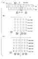
다음으로, 조명 장치(IU)에 대해 보다 상세하게 설명한다. 도 4는 본 실시 형태에 의한 조명 장치(IU)를 나타내는 사시도, 도 5의 (A)는 조명 장치(IU)를 나타내는 측면도, 도 5의 (B)는 조명 장치(IU)를 나타내는 정면도이다. 도 6은 광원부(도광부(導光部), 광원측 광학계)(20)의 일례를 나타내는 평면도, 도 7은 조리개 부재를 나타내는 평면도이다. Next, the lighting apparatus IU will be described in more detail. Fig. 4 is a perspective view showing the lighting apparatus IU according to the present embodiment, Fig. 5 (A) is a side view showing the lighting apparatus IU, and Fig. 5 (B) is a front view showing the lighting apparatus IU. 6 is a plan view showing an example of a light source portion (light guide portion (light guide portion), light source side optical system) 20, and Fig. 7 is a plan view showing a diaphragm member.
도 4의 조명 장치(IU)는, 소정의 방향(Y축 방향)을 긴 길이로 하는 조명 영역(IR)을 형성한다. 조명 장치(IU)는, 노광 장치(EX)(도 2 참조)에서, 조명 영역(IR)의 긴 길이 방향이 주사 방향(X축 방향)과 거의 수직하게 되도록 배치된다. The illumination device IU of Fig. 4 forms an illumination area IR having a predetermined length (Y-axis direction) as a long length. The illumination device IU is arranged in the exposure apparatus EX (see Fig. 2) so that the long-length direction of the illumination area IR is substantially perpendicular to the scanning direction (X-axis direction).
조명 장치(IU)는, 광원부(20), 확대 광학계(21), 광 인티그레이터(22), 및 결상 광학계(23)를 구비한다. 광원부(20)로부터 출사한 조명광(L1)은, 확대 광학계(21)를 통과하여 광 인티그레이터(22)에 입사하고, 광 인티그레이터(22)로부터 출사한 후에 결상 광학계(23)를 통과하여, 조명 영역(IR)에 입사한다. The lighting apparatus IU includes a
또, 노광용의 조명광(L1)은, 예를 들면, 파장이 300nm 이상 400nm 이하의 광, 혹은 400nm 이상 500nm 이하의 광, 예를 들면 자외역(紫外域)에 있는 광이 이용된다. 그 때문에, 광원부(20), 확대 광학계(21), 광 인티그레이터(22), 결상 광학계(23)의 각각을 구성하는 광학 소자의 유리재는, 석영이라도 좋다. As the illumination light L1 for exposure, light having a wavelength of 300 nm or more and 400 nm or less, or light having a wavelength of 400 nm or more and 500 nm or less, for example, light in a ultraviolet region is used. Therefore, the glass material of the optical element constituting each of the
도 6의 광원부(20)는, 고체 광원(24)(광원)과, 고체 광원(24)에 접속된 복수의 광 파이버(25)를 구비한다. 여기에서는, 광원부(20)에 고체 광원(24)이 복수 마련되어 있고, 광 파이버(25)는, 고체 광원(24)과 1대 1의 대응으로 마련되어 있다. 고체 광원(24)은, 예를 들면, 레이저 다이오드(LD) 혹은 발광 다이오드(LED)이다. 광원부(20)는, 고체 광원(24)으로부터의 광을 광 인티그레이터(22)로 안내한다. 6 includes a solid-state light source 24 (light source) and a plurality of
광 파이버(25)(도 4, 도 5 참조)는, 도 6의 고체 광원(24)으로부터의 조명광(L1)을, 확대 광학계(21)를 매개로 하여 광 인티그레이터(22)로 안내한다. 복수의 광 파이버(25)의 각각은, 조명광(L1)이 출사하는 단부(26)를 가지며, 광 파이버(25)의 단부(26)는, 광 인티그레이터(22)의 입사단(入射端)(35)의 긴 길이 방향(장축 방향, 장축)을 따라서 소정의 피치(소정의 간격, 중심 사이 거리)로 배열되어 있다. 복수의 광 파이버(25)의 각각의 단부(26)에는, 광원상(像)(Im1)이 형성되며, 광원부(20)는, 복수의 광원상(Im1)을, 조명 영역(IR)의 긴 길이 방향에 대응하는 방향으로 소정의 피치로 늘어서도록 형성하고, 광 인티그레이터(22)에 공급한다. The optical fiber 25 (see Figs. 4 and 5) guides the illumination light L1 from the solid-
광 파이버(25)의 단부(26)는, 거의 원형 모양이며, 광원부(20)로부터 출사시의 조명광(L1)의 퍼짐각은, 광 파이버(25)의 입사단에 수렴하여 입사하는 광의 각도 특성(개구수)이나 광 파이버(25)의 지름(φ1) 등에 의해 정해진다. 확대 광학계(21)는, 광 인티그레이터(22)에 입사시의 조명광(L1)의 퍼짐각을 조정한다. 확대 광학계(21)는, 광원부(20)와 광 인티그레이터(22)와의 사이의 광로에 배치되어 있고, 광원부(20)가 형성한 광원상(Im1)을 확대함으로써 조명광(L1)의 퍼짐각을 조정한다. The
도 5의 (B)의 확대 광학계(21)는, 조명 영역(IR)의 긴 길이 방향으로 배열된 복수의 모듈(27)을 구비한다. 복수의 모듈(27)의 각각은, 광원부(20)의 광 파이버(25)와 1대 1의 대응으로 마련되어 있고, 대응 관계에 있는 광 파이버(25)의 광 출사측의 단부(26)의 상(像)을 형성한다. 즉, 확대 광학계(21)는, 광원상(Im1)을 확대한 2차 광원상(Im2)을 형성한다. 또, 설명에서 참조하는 각 도면에서는, 도면을 보기 쉽게 하기 위해서, 광원부(20)와 모듈(27)의 수를 적절히 줄여 나타내는 경우가 있다. The magnifying
복수의 모듈(27)의 각각은, 2차 광원상(Im2)을 형성하는 렌즈(28) 및 렌즈(29)와, 렌즈(30)를 구비한다. 렌즈(30)는, 렌즈(29)를 통과한 조명광(L1)을, 광 인티그레이터(22)의 입사단(35)에 들어가도록 집광한다. 렌즈(28), 렌즈(29), 및 렌즈(30)의 각각은, 예를 들면 구면 렌즈로 구성되지만, 비구면 렌즈 또는 자유 곡면 렌즈를 포함하고 있어도 괜찮다. Each of the plurality of
렌즈(28) 및 렌즈(29)는, 예를 들면, 텔레센트릭(telecentric) 광학계이며, 렌즈(28)의 전측(前側) 초점 위치는, 광 파이버(25)의 광 출사측의 단부(26)에 설정되고, 렌즈(29)의 전측 초점 위치는, 렌즈(28)의 후측(後側) 초점 위치에 설정된다. 광 파이버(25)의 단부(26)의 상(像)(2차 광원상(Im2))은, 렌즈(29)의 후측 초점 위치에 형성된다. 렌즈(30)는, 렌즈(29)와 광 인티그레이터(22)의 입사단(35)과의 사이의 광로에 배치되며, 예를 들면, 그 후측 초점 위치가 광 인티그레이터(22)의 입사단(35)에 설정된다. The
이러한 설정의 경우, 광 인티그레이터(22)의 입사단(35)의 위치에, 광 파이버(25)의 단부(26)의 상(像)(광원상)이 결상(結像)(수렴)하지만, 이것은 반드시 필요한 조건은 아니며, 광 인티그레이터(22)의 입사단(35)의 위치와 광원상이 형성되는 위치를, 렌즈(28 ~ 30)의 광축 방향으로 어긋나게 두어도 괜찮다. 예를 들면, 렌즈(30)의 후측 초점 위치는, 광 인티그레이터(22)의 입사단(35)의 위치로부터, 입사단(35)의 법선 방향으로 어긋나 있어도 괜찮다. In this setting, the image (light source image) of the
도 5의 모듈(27)은, 광 인티그레이터(22)에 입사시의 조명광(L1)의 퍼짐각을 규정하는 조리개 부재(31)를 포함한다. 조리개 부재(31)는, 이른바 개구 조리개이며, 예를 들면 확대 광학계(21)의 동면(瞳面)(2차 광원상(Im2))의 위치 또는 그 근방에 배치된다. 여기에서는, 조리개 부재(31)는, 광 파이버(25)의 광 출사측(고체 광원(24)측)의 단부와 광학적으로 공역인 위치에 배치되어 있다. The
도 7의 조리개 부재(31)는, 조명광(L1)이 통과하는 개구(31a)를 가진다. 개구(31a)는, 도 5의 복수의 모듈(27)의 배열에 대응하여, 조명 영역(IR)의 긴 길이 방향(Y축 방향)으로 복수 늘어서 있다. 개구(31a)는, 거의 원형이며, 조리개 부재(31)를 통과한 조명광(L1)의 XZ 면내의 퍼짐각과 YZ 면내의 퍼짐각을 거의 동일하게 규정한다. 또, 조리개 부재(31)는, 적절히, 생략할 수 있다. The
도 5의 (B)에서, 확대 광학계(21)의 복수의 모듈(27)은, 렌즈(28)가 Y축 방향으로 배열된 렌즈 어레이(32)와, 렌즈(29)가 Y축 방향으로 배열된 렌즈 어레이(33)와, 렌즈(30)가 Y축 방향으로 배열된 렌즈 어레이(34)로 구성되어 있다. 이와 같이, 확대 광학계(21)의 적어도 한 종류의 렌즈를 렌즈 어레이로 구성함으로써, 부품수를 줄일 수 있지만, 확대 광학계(21)의 적어도 한 종류의 렌즈는, 렌즈 어레이의 형태가 아니라도 괜찮고, 복수의 모듈(27)에서 서로 독립한 부품이라도 괜찮다. 5B, the plurality of
광 인티그레이터(22)(도 4 참조)는, 예를 들면 로드(rod) 렌즈와 같은 직방체(直方體) 모양의 광학 부재이다. 광 인티그레이터(22)는, 장방형의 입사단(장방형의 입사면, 제1 면)(35), 입사단(35)의 장변을 포함하는 내면(36), 입사단(35)의 단변을 포함하는 내면(37), 및 장방형의 출사단(장방형의 출사면, 제2 면)(38)을 가진다. 입사단(35)은, 광원부(20)로부터의 조명광(L1)이 입사하는 입사 영역을 포함하며, 출사단(38)은, 광 인티그레이터(22)의 내부를 통과한 조명광(L1)이 출사하는 출사 영역을 포함한다. 광 인티그레이터(22)는, 입사단(35)에 입사한 조명광(L1)을 내면(36)에서의 다중 반사에 의해서 출사단(38)으로 안내한다. The optical integrator 22 (see Fig. 4) is an optical member in the form of a rectangular parallelepiped, such as a rod lens. The
광 인티그레이터(22)에서 입사단(35)의 짧은 길이 방향(단축 방향, 단축)으로 퍼지는 조명광(L1)은, 후에 도 8의 (A)에 나타내지만, 짧은 길이 방향의 단부에 위치하는 내면(36)에서의 반사 횟수가 다른 복수의 광속을 포함하고 있다. 광 인티그레이터(22)를 통과하는 조명광(L1)은, 반사 횟수가 다른 복수의 광속이 출사단(38)에서 서로 겹침으로써, 출사단(38)의 짧은 길이 방향의 조도 분포가 균일하게 된다. 여기에서는, 조명광(L1)은, 복수의 모듈(27) 중 어느 것으로부터 출사한 조명광(L1)이라도, 내면(36)에서 반사하는 광속을 포함하고 있다. The illuminating light L1 spreading in the short longitudinal direction (short axis direction, short axis) of the
광 인티그레이터(22)에서 입사단(35)의 긴 길이 방향으로 퍼지는 조명광(L1)은, 후에 도 8의 (B)에 나타내지만, 그 출사원(元)의 모듈(27)의 Y축 방향의 위치에 따라서, 긴 길이 방향의 단부에 위치하는 내면(37)에서 일부의 광속이 반사하고, 다른 광속이 내면(37)에 입사하지 않는다. 예를 들면, 입사단(35)의 긴 길이 방향의 단부에 배치되어 있는 모듈(27)로부터의 조명광(L1)은, 내면(37)에 입사하여 반사하는 광속을 포함하지만, 입사단(35)의 긴 길이 방향의 중앙부에 배치되어 있는 모듈(27)로부터의 조명광(L1)은, 내면(37)에 입사하는 광속을 실질적으로 포함하지 않는다. 여기에서는, 입사단(35)의 긴 길이 방향의 중앙부에 배치되어 있는 모듈(27)로부터의 조명광(L1)의 대부분은, 내면(37)에서 반사하지 않고 광 인티그레이터(22)의 내부를 통과하여, 출사단(38)으로부터 출사한다. The illumination light L1 spreading in the longitudinal direction of the
광 인티그레이터(22)는, 짧은 길이 방향에 대응하는 X축 방향(XZ면내)과 긴 길이 방향에 대응하는 Y축 방향(YZ면내)의 각각에서의 조명광(L1)의 퍼짐각을, 거의 변화시키지 않는다. 즉, 광 인티그레이터(22)에서의 조명광(L1)의 X축 방향의 퍼짐각은, 입사단(35)으로의 입사시와 출사단(38)으로부터의 출사시에 거의 동일하다. 또, 광 인티그레이터(22)에서의 조명광(L1)의 Y축 방향의 퍼짐각은, 입사단(35)으로 입사시와 출사단(38)으로부터의 출사시에 거의 동일하다. 광 인티그레이터(22)로부터 출사한 조명광(L1)은, 결상 광학계(23)에 입사한다. The
결상 광학계(23)는, 출사단(38)의 긴 길이 방향에 관한 굴절력에 비해, 출사단(38)의 짧은 길이 방향에 관한 굴절력이 크다. 결상 광학계(23)는, 예를 들면, 한 쌍의 원통형 렌즈(원통 렌즈)로 구성된다. 결상 광학계(23)의 원통형 렌즈의 모선(母線)은, 예를 들면, 출사단(38)의 긴 길이 방향과 거의 평행하게 설정된다. The imaging
결상 광학계(23)는, 광 인티그레이터(22)의 출사단(38)의 짧은 길이 방향에 평행 또한 긴 길이 방향에 수직인 임의의 면 상의 광속에 관하여 결상 작용을 가진다. 결상 광학계(23)는, 광 인티그레이터(22)의 출사단(38)의 짧은 길이 방향에 관하여 출사단(38)과 공역인 공역면(23a)(조명 영역(IR))을 형성한다. 예를 들면, 조명 장치(IU)를 Y축 방향으로부터 보았을 때에, 출사단(38)의 1점(Y축 방향에 평행한 선)으로부터 출사한 광속은, 공역면(23a) 상의 거의 1점(Y축 방향에 평행한 선) 상에 수렴한다. The imaging
이상과 같은 구성의 조명 장치(IU)는, 공역면(23a)(조명 영역(IR))이 마스크 패턴(M)(회전 드럼(DM)의 원통면(DMa))과 거의 동일 위치가 되도록 배치된다. 광 인티그레이터(22)의 출사단(38)에서 짧은 길이 방향의 조도 분포는, 내면(36)에서의 다중 반사에 의해 균일화되어 있고, 결상 광학계(23)가 짧은 길이 방향에 관하여 출사단(38)과 조명 영역(IR)을 광학적으로 공역으로 하기 때문에, 조명 영역(IR)에서 짧은 길이 방향의 조도 분포가 균일하게 된다. 또, 조명 영역(IR)에서 긴 길이 방향의 조도 분포는, 복수의 광원부(20)의 각각에 유래하는 조도 분포가 긴 길이 방향으로 어긋나 겹침으로써 균일화된다. 그 때문에, 조명 장치(IU)는, 조명 영역(IR)을 균일한 밝기로 조명할 수 있다. The illumination device IU having the above configuration is arranged such that the
다음으로, 조명 장치(IU)에 의한 조명 방법에 대해 보다 상세하게 설명한다. 여기에서는, 각종의 부재의 치수, 초점 거리 등의 값을 들어 설명하지만, 이들의 값은 일례로서 적절히 변경할 수 있다. Next, the lighting method by the lighting apparatus IU will be described in more detail. Here, the values of the various members, the focal length, and the like are described, but these values can be appropriately changed as an example.
도 6의 광원부(20)의 고체 광원(24)은, 예를 들면 레이저 다이오드이며, 조명광(L1)으로서 파장이 약 403nm 정도의 레이저광을 발(發)하고, 출력이 약 0.25W 정도이다. 광원부(20)에는 예를 들면 83개의 고체 광원(24)이 마련되고, 이들 83개의 고체 광원(24)의 총 출력은, 약 20.075W이다. 광 파이버(25)는, 예를 들면, 고체 광원(24)과 동일 수(83개)로 마련되고, 그 지름(φ1)이 약 0.3mm이다. 이 예에서, 광원부(20)의 광 파이버(25)로부터 출사하는 조명광(L1)의 퍼짐각(각도 특성)은, NA(개구수)로 환산한 값으로 약 0.2이다. The solid-
이하의 설명에서, 광(예를 들면 조명광(L1))의 퍼짐각을 NA로 환산한 값을, 적절히, 광(예를 들면 조명광(L1))의 NA 환산값이라고 한다. 또, XZ 면내에서 X축 방향으로 퍼지는 광(광속)의 NA 환산값을 X축 방향의 NA 환산값, YZ 면내에서 Y축 방향으로 퍼지는 광(광속)의 NA 환산값을 Y축 방향의 NA 환산값이라고 하는 것이 있다. In the following description, a value obtained by converting the spread angle of light (for example, illumination light L1) into NA is suitably referred to as an NA-converted value of light (for example, illumination light L1). The NA converted value of light (light flux) spreading in the X axis direction in the XZ plane is converted into the NA converted value in the X axis direction, the NA converted value of light (flux) spreading in the Y axis direction in the YZ plane is converted into the NA converted in the Y axis direction Value.
조명 장치(IU)로부터의 출사시의 조명광(L1)의 퍼짐각, 즉 조명 영역(IR)에 입사시의 조명광(L1)의 퍼짐각은, 조명 장치(IU)의 용도 등에 따라 설정된다. 예를 들면, 노광 장치(EX)에서, 조명 장치(IU)로부터 출사시의 조명광(L1)의 퍼짐각은, 노광 장치(EX)의 해상도(투영 패턴의 선폭) 등에 따라 선택된다. 여기에서는, 노광 장치(EX)의 해상도가 수㎛ 정도이며, 조명 장치(IU)로부터 사출되었을 때의 조명광(L1)의 NA 환산값이 0.04로 설정되어 있는 것으로 한다. The spread angle of the illumination light L1 at the time of exit from the illumination device IU, that is, the spread angle of the illumination light L1 at the time of incidence on the illumination area IR, is set according to the use or the like of the illumination device IU. For example, in the exposure apparatus EX, the spread angle of the illumination light L1 at the time of exiting from the illumination device IU is selected in accordance with the resolution (line width of the projection pattern) of the exposure apparatus EX and the like. Here, it is assumed that the resolution of the exposure apparatus EX is about several micrometers, and the NA converted value of the illumination light L1 when it is emitted from the illumination device IU is set to 0.04.
도 5의 확대 광학계(21)의 각 모듈(27)은, 광원부(20)가 형성하는 광원상(Im1)을 N배(예를 들면 5배)로 확대한다. 이것에 의해, 확대 광학계(21)로부터 출사시의 조명광(L1)의 NA 환산값은, 확대 광학계(21)에 입사시의 조명광(L1)의 NA 환산값(예를 들면 0.2)의 1/N배(여기에서는, 0.2/5=0.04)가 된다. 이러한 모듈(27)은, 예를 들면, 렌즈(28)의 초점 거리(f1)를 약 3mm, 렌즈(29)의 초점 거리(f2)를 약 15mm, 렌즈(30)의 초점 거리(f3)를 약 18.75mm로 함으로써 실현할 수 있다. Each
도 8 및 도 9는, 조명 방법을 설명하기 위한 도면이다. 상세하게는, 도 8의 (A)는, 광원상(2차 광원상(Im2))으로부터의 광속을 Y축 방향으로부터 본 측면도, 도 8의 (B)는 광원상(2차 광원상(Im2))으로부터의 광속을 X축 방향으로부터 본 정면도, 도 9는 조명 영역(IR)으로부터 광원상(Im1)(2차 광원상(Im2))을 본 도면이다. Figs. 8 and 9 are views for explaining an illumination method. Fig. 8A is a side view of the light beam from the light source image (secondary light source image Im2) viewed from the Y axis direction, and FIG. 8B is a side view of the light source image (secondary light source image Im2 9 is a view showing the light source image Im1 (secondary light source image Im2) from the illumination area IR.
도 8의 광 인티그레이터(22)는, 예를 들면, 짧은 길이 방향(X축 방향)의 치수가 약 2.5mm, 긴 길이 방향(Y축 방향)의 치수가 약 250mm, 짧은 길이 방향 및 긴 길이 방향에 수직인 방향(Z축 방향)의 치수가 약 125mm이다. 광 인티그레이터(22)에 입사시의 조명광(L1)의 퍼짐각(각도 특성)은, 확대 광학계(21)로부터 출사시의 조명광(L1)의 퍼짐각과 거의 동일하고, 예를 들면 NA 환산값으로 0.04 정도이다. The
이 조건에서, 조명광(L1)은, 도 8의 (A)와 같이 Y축 방향으로부터 보면, 광 인티그레이터(22)의 내면(36)에서의 반사 횟수가 0회의 광속, 1회의 광속, 및 2회의 광속을 포함하고, 이들 광속은, 출사단(38)에서 서로 겹쳐진다. 8 (A), the number of reflection times of the illumination light L1 on the
출사단(38)의 짧은 길이 방향에 관한 조명광(L1)의 NA 환산값(X축 방향의 NA 환산값)은, 입사단(35)으로의 입사시와 출사단(38)으로부터의 출사시에 거의 동일하며, 예를 들면 0.04 정도이다. 또, 출사단(38)의 긴 길이 방향에 관한 조명광(L1)의 NA 환산값(Y축 방향의 NA 환산값)은, 입사단(35)으로의 입사시와 출사단(38)으로부터의 출사시에 거의 동일하며, 예를 들면 0.04 정도이다. 이와 같이, 도 8의 예에서는, 광 인티그레이터(22)로부터 출사시의 조명광(L1)의 퍼짐각이 긴 길이 방향과 짧은 길이 방향에서 등방적이고, 결상 광학계(23)로의 입사시의 조명광(L1)의 퍼짐각은, 긴 길이 방향과 짧은 길이 방향에서 등방적이 된다. The NA converted value (the NA converted value in the X axis direction) of the illumination light L1 in the short-length direction of the emitting
결상 광학계(23)로의 입사시에서의 조명광(L1)의 퍼짐각이 Z축의 둘레로 등방적인 경우에, X축 방향(짧은 길이 방향)에 관한 결상 광학계(23)의 배율은, 예를 들면 등배로 설정된다. 이러한 결상 광학계(23)는, 예를 들면, 한 쌍의 원통형 렌즈의 XZ 평면에서의 초점 거리를 거의 동일(예를 들면 약 15mm)하게 함으로써 실현할 수 있다. The magnification of the imaging
결상 광학계(23)로부터 출사시에서의 조명광(L1)의 짧은 길이 방향의 퍼짐각(X축 방향의 NA 환산값)은, 결상 광학계(23)의 배율이 등배이므로, 결상 광학계(23)로의 입사시에서의 조명광(L1)의 짧은 길이 방향의 퍼짐각(X축 방향의 NA 환산값)과 거의 동일하게 된다. Since the magnification of the imaging
결상 광학계(23)로부터 출사시의 조명광(L1)의, 긴 길이 방향에서의 퍼짐각(Y축 방향의 NA 환산값)은, 결상 광학계(23)가 YZ 평면에 관하여 굴절률을 거의 가지고 있지 않기 때문에, 결상 광학계(23)로의 입사시의 조명광(L1)의, 긴 길이 방향에서의 퍼짐각(Y축 방향의 NA 환산값)과 거의 동일하게 된다. The spreading angle (converted value in the Y-axis direction in the Y-axis direction) of the illumination light L1 at the time of emergence from the imaging
이와 같이, 결상 광학계(23)로부터 출사시의 조명광(L1)의 퍼짐각을 등방적으로 함으로써, 조명 영역(IR)에 입사시의 조명광(L1)의 퍼짐각을 등방적으로 할 수 있다. 그 때문에, 노광 장치(EX)에서는, 노광 패턴의 선폭을, 짧은 길이 방향(X축 방향)과 긴 길이 방향(Y축 방향)으로 일치시키는 것이 용이하게 된다. As described above, by making the spread angle of the illumination light L1 at the time of emergence from the imaging
다음으로, 조명 영역(IR)의 조도 분포에 대해 설명한다. 이하의 설명에서, 조명 영역(IR) 중, 광원부(20)가 형성하는 복수의 광원상(Im1) 중 하나로부터의 조명광(L1)이 입사하는 입사 영역을, 적절히, 부분 조명 영역이라고 한다. 도 8의 (B)에 나타내는 바와 같이, 부분 조명 영역(IRa)은, 확대 광학계(21)에서의 복수의 2차 광원상(Im2) 중 하나로부터의 조명광(L1)이 입사하는 입사 영역으로 정의해도 괜찮다. 여기에서는, 부분 조명 영역(IRa)은, 도 5에 나타낸 1개의 광 파이버(25)의 사출측의 단부(26)로부터 출사한 조명광(L1)이 입사하는, 공역면(23a)(조명 영역(IR)) 상의 일부의 영역에 상당한다. Next, the illuminance distribution of the illumination area IR will be described. The incident region where the illumination light L1 from one of the plurality of light source images Im1 formed by the
확대 광학계(21)의 조리개 부재(31)(도 5 및 도 7 참조)는, 광 파이버(25)의 출사측의 단부(26)와 광학적으로 공역인 위치에 배치되어 있고, 조리개 부재(31)의 개구(31a)가 거의 원형이므로, 조명광(L1)의 광 강도 분포는, NA 환산값으로 0.04에 상당하는 퍼짐각에서 가우스(Gauss) 분포로 생각해도 좋다. 따라서, 조리개 부재(31)(개구(31a))의 1점으로부터의 광속은, 렌즈(30)의 초점면(焦点面)에서, 가우스 분포와 같은 조도 분포를 형성하며, 예를 들면 스폿(spot) 지름(φ2)이 약 1.5mm의 범위로 넓어진다. 또, 렌즈(30)의 초점면이 광 인티그레이터(22)의 입사단(35)과 거의 동일 위치인 경우에, 입사단(35)의 짧은 길이 방향의 치수(여기에서는 약 2.5mm)를, 스폿 지름(φ2=1.5mm) 이상으로 함으로써, 입사단(35)에서의 '비네팅(vignetting)'을 억제할 수 있다. The diaphragm member 31 (see Figs. 5 and 7) of the magnifying
광원부(20)로부터 출사하여 1개의 모듈(27)을 통과한 조명광(L1)은, 도 8의 (A)에 나타내는 바와 같이, 광 인티그레이터(22)의 내면(36)에서의 다중 반사에 의해, 출사단(38)에서 짧은 길이 방향의 조도 분포가 균일하게 된다. 여기에서는, 출사단(38)의 짧은 길이 방향으로 퍼지는 조명광(L1)은, 내면(36)에서의 반사 횟수가 0회인 광속, +X측의 내면(36) 또는 -X측의 내면(36)에서의 반사 횟수가 1회인 광속, +X측의 내면(36) 또는 -X측의 내면(36)에서의 반사 횟수가 2회인 광속을 포함하며, 이들 5개의 광속이 출사단(38)에서 서로 겹쳐진다. The illumination light L1 emitted from the
내면(36)에서 반사한 광속은, 광원상(Im1)의 허상(虛像)(Im3)으로부터의 광속에 상당하고, 출사단(38)의 각 점에 입사하는 광속은, 광원상(Im1)의 실상(實像)으로부터의 광속과, 내면(36)이 형성하는 4개의 허상(Im3)으로부터의 광속이 서로 겹쳐진 광속에 상당한다. 그 때문에, 도 9에 나타내는 바와 같이, 조명 영역(IR)의 1점으로부터 광원부(20)측을 보면, 5개의 광원상(Im1)(실상 또는 허상)이 X축 방향으로 늘어서게 된다. The light beam reflected by the
또, 도 9의 예에서는, Y축 상의 광원상(Im1)이 실상이며, 그 외의 광원상(Im1)이 허상(Im3)이다. 또, 도 8의 (A)에서는 허상(Im3)을 모식적으로 나타내고 있지만, 허상(Im3)은, 예를 들면, 2차 광원상(Im2)과 동일 면, 또는 2차 광원상(Im2)과 공역인 면(광 파이버(25)의 출사측의 단부(26)와 동일 면)에 배치된다. In the example of Fig. 9, the Y-axis light source image Im1 is the real image, and the other light source image Im1 is the virtual image Im3. The virtual image Im3 is schematically shown in Fig. 8 (A), but the virtual image Im3 may be the same image as the secondary image source image Im2 or the secondary image source image Im2, (The same side as the
또, 광원부(20)로부터 출사하여 1개의 모듈(27)을 통과한 조명광(L1)은, 도 8의 (B)에 나타내는 바와 같이, 입사단(35)의 긴 길이 방향으로 퍼지면서 광 인티그레이터(22)의 내부를 통과하여, 부분 조명 영역(IRa)에 입사한다. 부분 조명 영역(IRa)은, 예를 들면 Y축 방향으로 길이가 긴 거의 직사각형 모양의 영역이며, 광원부(20)가 형성하는 광원상(Im1)의 실상과 1대 1의 대응으로 형성된다. 즉, 부분 조명 영역(IRa)은, 확대 광학계(21)의 각 모듈(27)이 형성하는 2차 광원상(Im2)과 1대 1의 대응으로 형성된다. 8 (B), the illumination light L 1 emitted from the
도 10은, 조도 분포를 설명하기 위한 그래프이다. 상세하게는, 도 10의 (A)는, 모듈(27) 마다의 조명 영역(IR)(부분 조명 영역(IRa))의 조도 분포 B1을 나타내는 그래프이며, 가로축은 짧은 길이 방향의 위치, 세로축은 조도의 상대값을 나타낸다. 도 10의 (B)는, 복수의 부분 조명 영역(IRa)에 의한 조명 영역(IR)의 조도 분포 B2를 나타내는 그래프이며, 가로축은 긴 길이 방향의 위치, 세로축은 긴 길이 방향의 각 위치에서의 짧은 길이 방향의 조도를 평균화한 값의 상대값을 나타낸다. 10 is a graph for explaining the illuminance distribution. 10A is a graph showing the illuminance distribution B1 of the illumination area IR (partial illumination area IRa) for each
도 10의 (A)에 나타내는 바와 같이, 각 부분 조명 영역(IRa)의 조도 분포 B1은, 가우스 분포와 같은 분포이다. 조명 영역(IR)에서, 부분 조명 영역(IRa)은, 각각이 이웃하는 부분 조명 영역(IRa)과 서로 겹치도록, Y축 방향으로 배열된다. 도 10의 (B)에 나타내는 바와 같이, 조명 영역(IR)의 조도 분포 B2는, 부분 조명 영역(IRa)의 조도 분포 B1이 Y축 방향으로 어긋나 겹쳐진 분포가 된다. 그 때문에, 조명 영역(IR)의 조도 분포 B2는, 부분 조명 영역(IRa)을 소정의 피치로 배치함으로써, 이른바 톱 해트(top hat)형의 분포가 되며, Y축 방향의 단부를 제외하면 거의 균일한 조도가 된다. As shown in Fig. 10 (A), the illuminance distribution B1 of each partial illumination region IRa is the same distribution as the Gaussian distribution. In the illumination area IR, the partial illumination area IRa is arranged in the Y-axis direction so as to overlap with the neighboring partial illumination area IRa. As shown in Fig. 10 (B), the illuminance distribution B2 of the illumination area IR is a distribution in which the illuminance distribution B1 of the partial illumination area IRa is shifted in the Y-axis direction and overlapped. Therefore, the illuminance distribution B2 of the illumination region IR becomes a so-called top hat type distribution by disposing the partial illumination regions IRa at a predetermined pitch, Resulting in uniform illumination.
부분 조명 영역(IRa)의 Y축 방향의 피치는, 광원부(20)가 형성하는 광원상(Im1)(광 파이버(25)의 사출측의 단부(26))의 Y축 방향의 피치(단부(26)의 중심 사이 거리)에 따른 값이 된다. 부분 조명 영역(IRa)의 Y축 방향의 피치는, 부분 조명 영역(IRa)의 중심 위치로부터, 그 이웃하는 부분 조명 영역(IRa)의 중심 위치까지의 거리(중심 사이 거리)이며, 그 외의 요소의 피치도 동일하게 정의할 수 있다. The pitch in the Y axis direction of the partial illumination region IRa is a pitch in the Y axis direction of the light source image Im1 (the exit side end 26 of the optical fiber 25) formed by the
광원부(20)가 형성하는 복수의 광원상(Im1)의 Y축 방향의 피치는, 공역면(23a)(조명 영역(IR))에서의 Y축 방향의 조도 분포가 균일하게 되도록 설정되어 있다. 광 파이버(25)의 사출측의 단부(26), 렌즈(28), 렌즈(29), 및 렌즈(30)의 각각의 Y축 방향의 피치는, 예를 들면 3mm이다. The pitches of the plurality of light source images Im1 formed by the
또, 원하는 치수의 조명 영역(IR)을 형성하려면, 광 파이버(25), 및 확대 광학계(21)의 모듈(27)을, 조명 영역(IR)의 Y축 방향의 치수를 따른 수만큼 Y축 방향으로 소정의 피치로 배열하면 된다. The
이 조명 장치(IU)에서는, 결상 광학계(23)의 원통형 렌즈가 YZ면에 관하여 굴절력을 거의 가지고 있지 않기 때문에, 조명광(L1)은, 광 인티그레이터(22)의 Y축 방향의 단부로부터 외측으로 예를 들면 약 14mm 정도 퍼지게 된다. 광 인티그레이터(22)의 외측으로 퍼지는 조명광(L1)에 의해서 비추어지는 영역은, 다른 영역과 조도 분포가 불균일하게 되는 경우가 있으며, 조명 영역(IR)으로서 이용하지 않아도 괜찮다. In this illumination apparatus IU, since the cylindrical lens of the imaging
도 8의 (B)의 예에서는, 조명 영역(IR)의 1점에 입사하는 광속은, Y축 방향으로 늘어서는 5개의 모듈(27)로부터의 광속을 서로 겹친 광속이다. 그 때문에, 도 9에 나타내는 바와 같이, 조명 영역(IR)의 1점으로부터 광원부(20)측을 보면, 5개의 광원상(Im1)이 Y축 방향으로 늘어서게 된다. 조명 영역(IR) 중 Y축 방향의 단부를 제외한 영역의 각 점에는, X축 방향으로 5행, Y축 방향으로 5열인 25개의 광원상(Im1)의 배열로부터의 광속에 상당하는 광속이 입사하게 된다. In the example of FIG. 8 (B), the light beam incident on one point of the illumination area IR is a light beam which is obtained by superimposing the light beams from the five
본 실시 형태에서, 조명 영역(IR)의 짧은 길이 방향의 조도 분포는, 광 인티그레이터(22)의 내면(36)에서의 다중 반사에 의해 균일화되고, 조명 영역(IR)의 긴 길이 방향의 조도 분포는, 복수의 광원상(Im1)으로부터의 광속이 어긋나 겹쳐짐으로써 균일화된다. 이러한 조명 장치(IU)는, 소정 방향으로 늘어서는 부분 조명 영역(IRa)의 수를 적절히 조정함으로써, 조명 영역(IR)을 소정 방향에서 원하는 길이로 하면서, 조명 영역(IR)을 균일한 밝기로 조명할 수 있다. In the present embodiment, the illuminance distribution in the short-length direction of the illumination region IR is made uniform by the multiple reflection at the
본 실시 형태에서, 노광 장치(EX)는, 주사 방향에 직교하는 방향의 조명 영역(IR)을 원하는 길이로 할 수 있으므로, 노광 처리의 처리 범위를 넓힐 수 있다. 결과적으로, 노광 장치(EX)는, 대형의 디바이스를 제조하기 위한 대형의 기판, 다면(多面)을 얻기 위한 대형의 기판 등을 효율 좋게 처리할 수 있다. In the present embodiment, the exposure apparatus EX can extend the processing range of the exposure processing since the illumination region IR in the direction orthogonal to the scanning direction can be set to a desired length. As a result, the exposure apparatus EX can efficiently process a large substrate for manufacturing a large-sized device, a large substrate for obtaining a multi-surface, and the like.
[제2 실시 형태][Second Embodiment]
다음으로, 제2 실시 형태에 대해 설명한다. 본 실시 형태에서 상술의 실시 형태와 동일한 구성에 대해서는, 동일 부호를 부여하여 그 설명을 간략화 혹은 생략하는 것이 있다. Next, the second embodiment will be described. In the present embodiment, the same components as those in the above-described embodiment are denoted by the same reference numerals, and the description thereof is simplified or omitted.
도 11은 본 실시 형태에 의한 노광 장치(EX)를 나타내는 측면도이다. 도 11의 노광 장치(EX)는, 도 2에 나타낸 회전 드럼(DP)을 대신하여 기판 스테이지(ST)를 구비한다. 기판 스테이지(ST)는, 기판(P)을 지지하는 기판 지지 부재이며, 노광 영역(PR)에서 기판(P)을 평면 모양으로 유지하도록 지지한다. 기판 스테이지(ST)는, 예를 들면 기판(P)의 이면을 에어 베어링의 층에 의해 비접촉으로 지지한다. 11 is a side view showing the exposure apparatus EX according to the present embodiment. The exposure apparatus EX in Fig. 11 has a substrate stage ST instead of the rotary drum DP shown in Fig. The substrate stage ST is a substrate supporting member for supporting the substrate P and supports the substrate P in a planar shape in the exposure region PR. The substrate stage ST, for example, supports the back surface of the substrate P in a noncontact manner by a layer of an air bearing.
노광 장치(EX)에서, 회전 드럼(DM)(마스크 패턴(M))과 기판 스테이지(ST)(기판(P))와의 사이의 광로에는, 조리개 부재(40)가 마련되어 있다. 조리개 부재(40)는, 이른바 시야 조리개여, 조명 장치(IU)로부터 출사하여 마스크 패턴(M)을 경유한 광(노광광)의 통과 범위를 규정하는 것에 의해서, 기판(P) 상의 광의 입사 범위를 규정한다. 노광 장치(EX)는, 조리개 부재(40)에 의해 노광 영역(PR)의 범위를 정밀도 좋게 규정할 수 있지만, 조리개 부재(40)를 구비하지 않아도 괜찮다. In the exposure apparatus EX, a
도 12의 (A)는 조명 장치(IU)를 나타내는 측면도, 도 12의 (B)는 조명 장치(IU)의 정면도, 도 13은 조리개 부재(31)를 나타내는 평면도이다. Fig. 12A is a side view showing the illuminator IU, Fig. 12B is a front view of the illuminator IU, and Fig. 13 is a plan view showing the
도 12의 조명 장치(IU)에서, 확대 광학계(21)가 조명광(L1)을 짧은 길이 방향(X축 방향)으로 넓히는 배율은, 확대 광학계(21)가 조명광(L1)을 긴 길이 방향(Y축 방향)으로 넓히는 배율 보다도 크다. 이러한 확대 광학계(21)는, 예를 들면, 렌즈(28)가 구면 렌즈로 구성되고, 렌즈(29)가 원통형 렌즈 및 구면 렌즈로 구성되지만, 렌즈(29)가 토릭 렌즈(toric lens)로 구성되어 있어도 괜찮다. In the illumination device IU of Fig. 12, the magnification that the magnifying
확대 광학계(21)의 배율이 X축 방향과 Y축 방향에서 다르므로, 광 파이버(25)의 단부(26)가 거의 원형인 경우에, 확대 광학계(21)가 형성하는 상(像)(도 13의 2차 광원상(Im2))은, X축 방향에 평행한 단축과 Y축 방향에 평행한 장축을 가지는 타원 모양이 된다. 광 파이버(25)의 단부(26)의 지름을 φ1, 확대 광학계(21)가 조명광(L1)을 X축 방향으로 넓히는 배율을 M1x, 확대 광학계(21)가 조명광(L1)을 Y축 방향으로 넓히는 배율을 M1y로 하면, 2차 광원상(Im2)의 단축은 M1x×φ1, 2차 광원상(Im2)의 장축은 M1y×φ1이 된다. 예를 들면, 광 파이버(25)의 단부(26)의 지름(φ1)이 0.3mm, M1x가 3배, M1y가 5배인 경우에, 2차 광원상(Im2)의 단축은 0.9mm, 2차 광원상(Im2)의 장축은 1.5mm가 된다. The magnification of the magnifying
확대 광학계(21)에 의해서 2차 광원상(Im2)이 형성되는 면(동면(41))의 위치 또는 그 근방에는, 도 13에 나타내는 바와 같은 조리개 부재(31)가 마련되어 있다. 조리개 부재(31)는, 이른바 개구 조리개로서, 예를 들면 2차 광원상(Im2)과 거의 서로 닮은 타원 모양의 개구(31a)를 가진다. 개구(31a)는, 예를 들면, 단축의 방향이 2차 광원상(Im2)과 거의 동일하게 설정되고, 장축의 방향이 2차 광원상(Im2)과 거의 동일하게 설정된다. 여기에서는, 개구(31a)는, 2차 광원상(Im2)과 거의 동일 치수로 형성되어 있다. 또, 조리개 부재(31)는, 개구(31a)가 2차 광원상(Im2) 보다도 작아도 좋고, 생략되어 있어도 괜찮다. A
2차 광원상(Im2)으로부터의 조명광(L1)은, 확대 광학계(21)의 렌즈(30)를 통과하여, 광 인티그레이터(22)의 입사단(35)에 입사한다. 입사단(35)에 입사시에서의 조명광(L1)의 퍼짐각(각도 특성)은, 2차 광원상(Im2)의 형상 또는 조리개 부재(31)의 형상에 의존한다. 2차 광원상(Im2)의 X축 방향의 치수(단축)가 Y축 방향의 치수(장축) 보다도 작기 때문에, 광 인티그레이터(22)에서의 조명광(L1)의 퍼짐각은, X축 방향의 퍼짐각이 Y축 방향의 퍼짐각 보다도 작게 된다. 즉, 확대 광학계(21)('집광 광학계'로도 부름)는, 광 인티그레이터(22)의 입사단(35)을 향하는 광의 입사단(35)의 긴 길이 방향(Y방향)에 관한 각도 특성과 짧은 길이 방향(X방향)에 관한 각도 특성을 다르게 하도록 설정된다. 예를 들면, 광 인티그레이터(22)에서, 조명광(L1)의 X축 방향의 NA 환산값은 약 0.024이며, 조명광(L1)의 Y축 방향의 NA 환산값은 0.04이다. The illumination light L1 from the secondary light source image Im2 passes through the
광 인티그레이터(22)에서, 입사단(35)의 짧은 길이 방향으로 퍼지는 조명광(L1)(도 12의 (A) 참조)은, 내면(36)에서 반사하여 출사단(38)으로 안내되며, 내면(36)에서의 다중 반사에 의해 출사단(38)에서의 조도가 균일화된다. 출사단(38)으로부터 출사시에서의 조명광(L1)의 짧은 길이 방향의 퍼짐각은, 입사단(35)으로의 입사시와 거의 동일하며, NA 환산값으로 예를 들면 0.024이다. In the
또, 광 인티그레이터(22)의 입사단(35)의 위치와, 광 파이버(25)의 단부(26)의 상(像)이 결상하는 위치는, 일치하고 있지 않아도 좋으며, 예를 들면, 확대 광학계(21)의 렌즈(30)의 광축에 평행한 방향에서 소정의 범위에서 어긋나 있어도 괜찮다. The position of the
또, 입사단(35)의 긴 길이 방향으로 퍼지는 조명광(L1)(도 12의 (B) 참조)은, 그 적어도 일부가 내면(37)에 입사하지 않고 광 인티그레이터(22)의 내부를 통과하여, 출사단(38)으로부터 출사한다. 출사단(38)으로부터 출사시에서의 조명광(L1)의 짧은 길이 방향의 퍼짐각은, 입사단(35)으로의 입사시와 거의 동일하며, NA 환산값으로 예를 들면 0.04이다. The illumination light L1 (refer to FIG. 12 (B)) extending in the longitudinal direction of the incident end 35 passes through the interior of the
도 12의 결상 광학계(23)는, 광 인티그레이터(22)의 출사단(38)의 상(像)을 짧은 길이 방향(X축 방향)으로 축소하여 공역면(23a)(조명 영역(IR))에 형성한다. 결상 광학계(23)의 X축 방향의 배율 M2x는, 확대 광학계(21)가 조명광(L1)을 X축 방향으로 넓히는 배율을 M1x, 확대 광학계(21)가 조명광(L1)을 Y축 방향으로 넓히는 배율을 M1y로 하면, M1x/M1y배이다. 예를 들면, M1x가 3배, M1y가 5배인 경우에, 결상 광학계(23)의 X축 방향의 배율은, 0.6배로 설정된다. 그 때문에, 조명 영역(IR)의 각 점에 입사하는 광속의 짧은 길이 방향의 NA 환산값은, 광 인티그레이터(22)로부터의 출사시에 대해서, 1/(M1x/M1y) 배가 된다. 예를 들면, 조명 영역(IR)의 각 점에 입사하는 광속의 짧은 길이 방향의 NA 환산값은, 0.024/0.6이 되고, 조명 영역(IR)의 각 점에 입사하는 광속의 긴 길이 방향의 NA 환산값와 거의 동일 값(0.04)이 된다. The imaging
본 실시 형태에서, 결상 광학계(23)는, 광 인티그레이터(22)의 출사단(38)의 상(像)을 짧은 길이 방향으로 축소하므로, 광 인티그레이터(22)의 폭(X축 방향의 치수)에 대해서 공역면(23a)의 폭이 좁게 된다. 예를 들면, 원통 모양으로 만곡한 마스크 패턴(M)을 이용하는 노광 장치(EX)에서, 공역면(23a)의 폭을 작게 하면, 마스크 패턴(M)의 형상과 공역면(23a)의 형상의 어긋남을 줄일 수 있고, 마스크 패턴(M)에서의 디포커스량(defocus量)을 줄일 수 있다. 또, 조명 영역(IR)의 폭에 비해 광 인티그레이터(22)의 폭을 크게 할 수 있고, 광 인티그레이터(22)의 강도를 확보하는 것이 용이하게 된다. 그 때문에, 예를 들면, 광 인티그레이터(22)를 Y축 방향으로 늘리는 것이 용이하게 되고, 조명 영역(IR)을 Y축 방향으로 늘리는 것이 용이하게 된다. In the present embodiment, the imaging
또, 본 실시 형태의 조명 장치(IU)는, 제1 실시 형태에서 설명한 바와 같이, 조명 영역(IR)의 조도 분포가 긴 길이 방향과 짧은 길이 방향의 각각에서 균일화되고, 조명 영역(IR)을 소정 방향에서 원하는 길이로 하면서 균일한 밝기로 조명할 수 있다. As described in the first embodiment, the illuminating device IU of the present embodiment is configured such that the illuminance distribution of the illumination area IR is uniformized in each of the long and short length directions, It is possible to illuminate uniform brightness while keeping the desired length in a predetermined direction.
[제3 실시 형태][Third embodiment]
다음으로, 제3 실시 형태에 대해 설명한다. 본 실시 형태에서 상술의 실시 형태와 동일한 구성에 대해서는, 동일 부호를 부여하여 그 설명을 간략화 혹은 생략하는 것이 있다. Next, the third embodiment will be described. In the present embodiment, the same components as those in the above-described embodiment are denoted by the same reference numerals, and the description thereof is simplified or omitted.
도 14는 본 실시 형태에 의한 노광 장치(EX)를 나타내는 측면도, 도 15는 조명 장치(IU)를 나타내는 상면도이다. 도 14의 조명 장치(IU)는, 제1 광학계(45), 제2 광학계(46), 및 결상 광학계(23)를 구비한다. 제1 광학계(45) 및 제2 광학계(46)는, 각각 조명광(L1)을 사출하고, 제1 광학계(45) 및 제2 광학계(46)로부터의 조명광(L1)은, 결상 광학계(23)를 매개로 하여 조명 영역(IR)에 입사한다. Fig. 14 is a side view showing the exposure apparatus EX according to the present embodiment, and Fig. 15 is a top view showing the lighting apparatus IU. 14 includes a first
제1 광학계(45)는, 광원부(20a)(제1 도광부), 확대 광학계(21a), 및 광 인티그레이터(22a)(제1 광 인티그레이터)를 구비한다. 광원부(20a) 및 확대 광학계(21a)는, 예를 들면, 제1 실시 형태와 동일한 구성이라도 좋다. 광원부(20a)로부터 출사한 조명광(L1)은, 확대 광학계(21a)를 매개로 하여 광 인티그레이터(22a)의 입사단(35a)에 입사한다. 광원부(20a), 확대 광학계(21a), 및 광 인티그레이터(22a)의 각각을 구성하는 광학 소자의 유리재는, 예를 들면 석영이라도 괜찮다. The first
도 14의 광 인티그레이터(22a)는, 절두체 모양(뿔모양의 윗부분을 자른 모양)의 부재로서, Y축 방향으로부터 본 측면이 거의 사다리꼴이다. 광 인티그레이터(22)는, YZ면에 거의 평행한 제1 면(47a)과, 제1 면(47a)에 대해서 비수직(예를 들면 약 45°)로 경사진 제2 면(47b)과, 제1 면(47a)에 거의 평행한 제3 면(47c)과, 제1 면(47a)에 거의 수직인 제4 면(47d)을 가진다. The
광 인티그레이터(22a)는, 제1 면(47a)의 일부에 광원부(20a)로부터의 조명광(L1)이 입사하도록 배치되어 있고, 광원부(20a)로부터의 조명광(L1)의 입사 영역의 적어도 일부가 입사단(35a)을 포함한다. 입사단(35a)은, 제1 면(47a)의 법선 방향으로부터 보아 제2 면(47b)과 겹치는 부분의 적어도 일부를 포함한다. 도 14의 광 인티그레이터(22a)에서, 입사단(35a)의 긴 길이 방향은 Y축 방향과 거의 평행이며, 입사단(35a)의 짧은 길이 방향은 Z축 방향과 거의 평행이다. The
입사단(35a)에 입사한 조명광(L1)은, 제2 면(47b)에서 반사하여 진행 방향이 절곡되며, 제1 면(47a) 및 제3 면(47c)에 대응하는 내면에서 반사함으로써, 제4 면(47d)으로 안내된다. 제4 면(47d)은 출사단(38a)을 포함하며, 광 인티그레이터(22a)의 내부를 통과한 조명광(L1)은, 출사단(38a)으로부터 출사한다. 도 14의 광 인티그레이터(22a)에서, 출사단(38a)의 긴 길이 방향은 Y축 방향과 거의 평행이며, 출사단(38a)의 짧은 길이 방향은 X축 방향과 거의 평행이다. The illumination light L1 incident on the
제2 광학계(46)는, 제1 광학계(45)와 동일한 구성이며, Y축 방향으로부터 보았을 때에 YZ면에 관하여 제1 광학계(45)와 대칭적으로 배치되어 있다. 제2 광학계(46)는, 광원부(20b)(제2 도광부), 확대 광학계(21b), 및 광 인티그레이터(22b)(제2 광 인티그레이터)를 구비하지만, 제1 광학계(45)와 공통되는 설명에 대해서는 간략화 혹은 생략한다. The second
광 인티그레이터(22a)와 광 인티그레이터(22b)는, 출사단(38a)(출사단(38b))의 짧은 길이 방향(X축 방향)으로 인접하여 배치되어 있고, 제3 면(47c)이 서로 접합되어 있다. 광 인티그레이터(22a)와 광 인티그레이터(22b)는, 예를 들면 굴절률이 1.46 이하의 접착제로 접합되어 있고, 각각의 제3 면(47c)에 대응하는 내면에서 조명광(L1)이 거의 전반사한다. The
도 15에 나타내는 바와 같이, 제1 광학계(45)의 광원부(20a)에서 광 파이버(25a)의 출사측의 단부(26a)는, 입사단(35a)의 긴 길이 방향(Y축 방향)으로 거의 일정한 피치 Py로 배열되어 있다. 또, 제2 광학계(46)의 광원부(20b)에서 광 파이버(25b)의 출사측의 단부(26b)는, 입사단(35b)의 긴 길이 방향(Y축 방향)으로 거의 일정한 피치 Py로 배열되어 있다. The
제1 광학계(45)의 광 파이버(25a)의 단부(26a)는, 입사단(35a)(입사단(35b))의 법선 방향(X축 방향)으로부터 보았을 때에, 제2 광학계(46)의 광 파이버(25b)의 단부(26b) 중 어느 것과도 Y축 방향의 위치가 겹치지 않도록 배치되어 있다. 제1 광학계(45)의 광 파이버(25a)의 단부(26a)와 제2 광학계(46)의 광 파이버(25b)의 단부(26b)는, Y축 방향으로부터 보아 교호(交互)로 늘어서 있으며, 단부(26a) 중 하나와 그 이웃하는 단부(26b)의 Y축 방향의 위치는, 단부(26a)의 피치 Py(단부(26b)의 피치 Py)의 절반정도 어긋나 있다. 즉, 단부(26a) 중 하나와 그 이웃하는 단부(26b)와의 Y축 방향의 위치의 어긋남 Δy는, 피치 Py의 절반(Py/2)과 거의 동일하다. The
광원부(20a)에서 복수의 광 파이버(25a)의 단부(26a)의 각각에는, 광원상(Im1a)이 형성되고, 광원부(20b)에서 복수의 광 파이버(25b)의 단부(26b)의 각각에는, 광원상(Im1b)이 형성된다. 그 때문에, 광원부(20a)에 의한 복수의 광원상(Im1a)은, 광원부(20b)에 의한 복수의 광원상(Im1b)과, 입사단(35a)(입사단(35b))의 긴 길이 방향(Y축 방향)의 위치가 겹치지 않도록 형성된다. A light source image Im1a is formed in each of the
도 14에 나타낸 광원부(20a)로부터의 조명광(L1)은, 광 인티그레이터(22a)의 내면에서의 다중 반사에 의해, 출사단(38a)의 짧은 길이 방향에서의 조도 분포가 출사단(38a)에서 균일화된다. 또, 광원부(20b)로부터의 조명광(L1)은, 광 인티그레이터(22b)의 내면에서의 다중 반사에 의해, 출사단(38b)의 짧은 길이 방향에서의 조도 분포가 출사단(38b)에서 균일화된다. 결상 광학계(23)는, 출사단(38a)(출사단(38b))의 짧은 길이 방향에 관하여, 광 인티그레이터(22a)의 출사단(38a) 및 광 인티그레이터(22b)의 출사단(38b)을 포함하는 면과 공역인 공역면(23a)을 형성한다. 그 때문에, 공역면(23a)(조명 영역(IR))에서 조명광(L1)의 조도 분포는, 출사단(38a)(출사단(38b))의 짧은 길이 방향에 대응하는 방향에서 균일하게 된다. The illumination light L1 from the
또, 도 8을 이용하여 설명한 바와 같이, 광원부(20a)가 형성하는 각 광원상(Im1a)으로부터의 광속은, 광 인티그레이터(22a)의 내부를 Y축 방향으로 퍼지면서 전파하여, 부분 조명 영역(IRa)에 입사한다. 부분 조명 영역(IRa)은, 이웃하는 부분 조명 영역(IRa)과 Y축 방향의 일부가 겹치도록, Y축 방향으로 배열된다. 이와 같이, 복수의 광원상(Im1a)에 유래하는 복수의 광속이 조명 영역(IR)에서 Y축 방향으로 어긋나 겹침으로써, 조명 영역(IR)의 Y축 방향의 조도 분포가 균일하게 된다. 제2 광학계(46)로부터의 조명광(L1)에 대해서도 마찬가지로 전파하여, 조명 영역(IR)의 Y축 방향의 조도 분포가 균일하게 된다. 8, the light flux from each light source image Im1a formed by the
다음으로, 조명 영역(IR)의 각 점에 입사하는 광속의 퍼짐각에 대해 설명한다. 도 9(도 8)를 참조하여 설명한 바와 같이, 조명 영역(IR)의 각 점에 입사하는 광속은, X축 방향과 Y축 방향으로 배열된 광원상의 실상 혹은 허상으로부터의 광속을 겹친 광속에 상당한다. 그 때문에, 조명 영역(IR)의 각 점에 입사하는 광속의 퍼짐각은, 각 점으로부터 광원부(20)측을 보았을 때의 광원상(Im1)의 실상 및 허상의 분포에 의해 정해진다. Next, the spreading angle of the light beam incident on each point of the illumination area IR will be described. As described with reference to Fig. 9 (Fig. 8), the light beam incident on each point of the illumination area IR corresponds to a light beam superimposed on a real image or a virtual image on a light source arranged in the X- do. Therefore, the spread angle of the light beam incident on each point of the illumination area IR is determined by the distribution of the real image and the virtual image of the light source image Im1 when the
도 16은, 본 실시 형태에 의한 조명 방법을 설명하기 위한 도면이다. 도 16의 (A)는, 이하의 설명에서 참조하는 조명 영역(IR)의 점 Q1, 점 Q2의 위치, 및 조명 영역(IR)의 법선 방향으로부터 보았을 때의 광원상(Im1)의 Y축 방향의 위치 관계를 나타내는 도면이다. 점 Q1와 점 Q2는, 광 인티그레이터(22a)의 출사단(38a)의 짧은 길이 방향(X축 방향)으로 늘어서는 점이며, 여기에서는, Y축 방향의 위치(좌표)가 광원부(20a)에 의한 광원상(Im1a)의 중심과 거의 동일한 것으로 한다. 16 is a view for explaining an illumination method according to the present embodiment. 16A shows the positions of the points Q1 and Q2 of the illumination area IR and the position of the point Q2 in the Y axis direction of the light source image Im1 when viewed from the normal direction of the illumination area IR Fig. The point Q1 and the point Q2 are points arranged in the short length direction (X axis direction) of the
광원부(20a)의 광 파이버(25a)로부터 출사시의 조명광(L1)의 퍼짐각은, 예를 들면, 광 파이버(25a)의 지름(φ1)이 약 0.3mm인 경우에, NA 환산값으로 0.2 정도이다. 예를 들면, 확대 광학계(21)의 X축 방향에 관한 배율(M1x)이 5배, 확대 광학계(21)의 X축 방향에 관한 배율(M1x)이 5배인 경우에, 확대 광학계(21)가 형성하는 2차 광원상(Im2)은, 스폿 지름(φ2)이 약 1.5mm인 원형 모양이 된다. 이러한 2차 광원상(Im2)으로부터의 조명광(L1)은, 광 인티그레이터(22a)에 입사시의 X축 방향(XZ면내)의 NA 환산값이 0.04 정도, Y축 방향(YZ면내)의 NA 환산값이 0.04 정도가 된다. The spreading angle of the illumination light L1 at the time of outputting from the
도 16의 (B)은, 조명 영역(IR) 상의 점 Q1으로부터 광원부(20a)를 보았을 때의 광원상(Im1a)의 실상 및 허상의 분포를 나타내는 도면, 도 16의 (C)은, 조명 영역(IR) 상의 점 Q2로부터 광원부(20b)를 보았을 때의 광원상(Im1b)의 실상 및 허상의 분포를 나타내는 도면이다. 16B is a diagram showing a real image and a virtual image distribution of the light source image Im1a when the
조명 영역(IR)으로부터 보았을 때의 광원상(Im1)의 실상과 허상의 X축 방향에서의 분포는, 광 인티그레이터(22)(도 8 참조)의 내면(36)에서의 조명광(L1)의 반사 횟수 등으로 정해진다. 내면(36)에서의 조명광(L1)의 반사 횟수는, 광 인티그레이터(22)에 입사시의 조명광(L1)의 X축 방향의 퍼짐각, 2개의 내면(36)의 X축 방향의 간격, 광 인티그레이터(22)의 Z축 방향의 치수 등에 의존한다. The actual image of the light source image Im1 viewed from the illumination area IR and the distribution of the virtual image in the X axis direction are the distribution of the illumination light L1 on the
여기서, 광 파이버(25)의 지름을 φ1, 광 파이버(25)의 단부(26)로부터 확대 광학계(21)에서 2차 광원상(Im2)이 형성되는 면(동면)까지의 XZ면에 관한 배율을 β1, 확대 광학계(21)의 렌즈(30)의 XZ면에 관한 초점 거리 f3, 결상 광학계(23)의 XZ면에 관한 배율을 β2로 하면, 조명 영역(IR)의 각 점(예를 들면, 점 Q1, 점 Q2)에 입사하는 광속의 X축 방향의 퍼짐각을 NA로 환산한 값(NAx)은, 하기의 식 (1)로 나타내어진다. Here, the diameter of the
NAx=(φ1×β1×0.5/f3)×1/β2 … (1)NAx = (? 1 占? 1 占 0.5 / f? 3 占 1 /? 2 占 ... (One)
식 (1)에서, 예를 들면, 광 파이버(25)의 지름(φ1)이 0.3mm, 확대 광학계(21)의 X축 방향의 배율(β1)이 5배, 확대 광학계(21)의 렌즈(30)의 초점 거리(f3)가 18.75mm, 결상 광학계(23)의 X축 방향의 배율(β2)이 1배라고 하면, NAx는 0.04가 된다. The diameter 1 of the
또, 조명 영역(IR)으로부터 보았을 때의 광원상(Im1)의 실상과 허상의 Y축 방향에서의 분포는, 광원부(20)가 형성하는 광원상(Im1)(광 파이버(25)의 단부(26))의 Y축 방향의 위치, 광 인티그레이터(22)에 입사시의 조명광(L1)의 퍼짐각, 광 인티그레이터(22)의 Z축 방향의 치수 등으로 정해진다. 여기서, 광원부(20)가 형성하는 광원상(Im1)의 Y축 방향의 피치를 Py, 광 파이버(25)로부터 출사시의 조명광(L1)의 Y축 방향의 NA 환산값을 NAy0, 광 파이버(25)의 단부(26)로부터 확대 광학계(21)에서 2차 광원상(Im2)이 형성되는 면(동면)까지의 YZ면에 관한 배율을 β3, 확대 광학계(21)의 렌즈(30)의 YZ면에 관한 초점 거리를 f4, 광 인티그레이터(22)의 입사단(35)으로부터 조명 영역(IR)까지의 광로 길이를 Lz로 하면, 제1 광학계(45)(광원부(20a))로부터 조명 영역(IR) 상의 점 Q1에 입사하는 광속의 Y축 방향의 NA 환산값(NAy1)은, 하기의 식 (2)로 나타내어진다. The actual image of the light source image Im1 and the distribution of the virtual image in the Y axis direction when viewed from the illumination area IR are the same as the light source image Im1 formed by the
NAy1=(Py×2+NAy0/β3×f4)/Lz … (2)NAy1 = (Pyx2 + NAy0 /? 3xf4) / Lz ... (2)
식 (2)에서, 광 파이버(25)의 단부(26)의 피치(Py)가 3mm, 광 파이버의 단부(26)로부터 출사시의 조명광(L1)의 NA 환산값(NAy0)이 0.2, 확대 광학계(21)의 Y축 방향의 배율(β3)이 5배, 확대 광학계(21)의 렌즈(30)의 초점 거리(f4)가 18.75mm, 광 인티그레이터(22)의 입사단(35)으로부터 조명 영역(IR)까지의 광로 길이(Lz)가 187.5mm라고 하면, NAy1는 0.036이 되어 NAx(0.04)와 다른 값이 된다. The pitch Py of the
이와 같이, 조명 영역(IR) 상의 각 점에 입사하는 광속은, 퍼짐각을 규정하는 요인이 X축 방향과 Y축 방향에서 다르므로, 퍼짐각이 X축 방향과 Y축 방향에서 다른 경우가 있을 수 있다. 퍼짐각의 이방성(異方性)은, 조명 장치(IU)의 용도 등에 따라 적절히 허용되지만, 본 실시 형태에서는, 도 15와 같이 광원부(20a)와 광원부(20b)에서, 광원상(Im1a)과 광원상(Im1b)과의 Y축 방향의 위치를 어긋나게 함으로써, 조명 영역(IR) 상의 각 점에 입사하는 광속의 퍼짐각을 X축 방향과 Y축 방향에서 등방적으로 하고 있다. As described above, in the light beam incident on each point on the illumination area IR, the spread angle is different in the X-axis direction and the Y-axis direction because the factors defining the spread angle are different in the X-axis direction and the Y- . The anisotropy of the spread angle is suitably permitted depending on the use of the lighting apparatus IU and the like. In the present embodiment, the light source image Im1a and the light source image Im2a in the
상세하게는, 도 16의 (B) 및 도 16의 (C)에 나타내는 바와 같이, 점 Q2로부터 광원부(20b)를 보았을 때의 광원상의 실상 및 허상은, 점 Q1으로부터 광원부(20a)를 보았을 때의 광원상의 실상 및 허상과 Y축 방향의 위치가 어긋나 있다. 여기에서는, 광원부(20a)에 의한 광원상(Im1a)과 광원부(20b)에 의한 광원상(Im1b)에서 Y축 방향의 위치가 피치(Py)의 절반정도 어긋나 있으므로, 조명 영역(IR)으로부터 본 광원상(Im1)의 실상 및 허상의 위치도, 광원상(Im1)의 Y축 방향의 피치(Py)의 절반정도 Y축 방향으로 어긋나게 된다. 그 때문에, 제2 광학계(46)(광원부(20b))로부터 조명 영역(IR) 상의 점 Q2에 입사하는 광속의 Y축 방향의 NA 환산값(NAy2)은, 하기의 식 (3)으로 나타내어진다. More specifically, as shown in Figs. 16B and 16C, the actual phase and the virtual phase of the light source when the
NAy2=(Py×2+Py×0.5)/Lz … (3)NAy2 = (Py x 2 + Py x 0.5) / Lz ... (3)
식 (3)에서, 피치(Py)가 3mm, 광 인티그레이터(22)의 입사단(35)으로부터 조명 영역(IR)까지의 광로 길이(Lz)가 187.5mm라고 하면, NAy2는 0.04가 된다. 여기서, 기판(P) 상의 점은, 점 Q1의 위치에서 제1 광학계(45)로부터의 광속으로 조명되고, 이 광속의 NAy1은 0.036이다. 또, 기판(P) 상의 이 점은, 기판(P)이 X축 방향으로 이동함으로써, 점 Q2의 위치에서 제2 광학계(46)로부터의 광속으로 조명되고, 이 광속의 NAy1은 0.04이다. 그 때문에, 기판(P) 상의 점에 입사하는 광속의 Y축 방향의 퍼짐각의 최대값은, NA 환산값으로 0.04가 되고, X축 방향의 NA 환산값(NAx=0.04)과 거의 동일하게 된다. Assuming that the pitch Py is 3 mm and the optical path length Lz from the
또, 점 Q2로서, Y축 방향의 위치(좌표)가 광원부(20b)에 의한 광원상(Im1b)의 중심과 거의 동일한 점을 선택하고, 이 점 Q2로부터 X축 방향의 위치가 어긋난 점을 Q1으로 한 경우를 상정(想定)한다. 이 경우에, 기판(P) 상의 점은, 점 Q1에서 제1 광학계(45)로부터의 광속으로 조명될 때의 Y축 방향의 NA 환산값이 0.04, 점 Q2에서 제2 광학계(46)로부터의 광속으로 조명될 때의 Y축 방향의 NA 환산값이 0.036이 된다. 그 때문에, 기판(P) 상의 점에 입사하는 광속의 Y축 방향의 퍼짐각의 최대값은, NA 환산값에서 0.04가 되고, X축 방향의 NA 환산값(NAx=0.04)과 거의 동일하게 된다. The position (coordinate) in the Y-axis direction is substantially the same as the center of the light source image Im1b by the
이와 같이, 광원부(20a)에 의한 복수의 광원상(Im1a)의 긴 길이 방향에서의 위치와, 광원부(20b)에 의한 복수의 광원상(Im1b)의 긴 길이 방향에서의 위치와의 어긋남량(Δy)은, 결상 광학계(23)를 매개로 하여 공역면(23a) 상의 각 점에 입사하는 광속의 퍼짐각이 긴 길이 방향과 짧은 길이 방향에서 등방적이 되도록 설정되어 있다. In this manner, the shift amount between the position of the plurality of light source images Im1a by the
도 17은, 본 실시 형태의 조명 장치(IU)의 구성에 기초한 시뮬레이션에 의해 얻어진 조도 분포의 일례를 나타내는 그래프이다. 도 17의 (A)는 짧은 길이 방향의 조도 분포를 나타내고, 세로축이 조도(단위면적당 광선 갯수), 가로축이 짧은 길이 방향(X축 방향)의 위치이다. 도 17의 (B)는 긴 길이 방향의 조도 분포를 나타내고, 세로축이 긴 길이 방향의 각 위치에서의 짧은 길이 방향의 조도의 적산값, 가로축이 긴 길이 방향(Y축 방향)의 위치이다. 도 17에 나타내는 바와 같이, 짧은 길이 방향과 긴 길이 방향의 각각에서, 균일한 조도가 얻어진다. Fig. 17 is a graph showing an example of the illuminance distribution obtained by simulation based on the configuration of the lighting apparatus IU of the present embodiment. Fig. Fig. 17A shows the illuminance distribution in the short-length direction, and the ordinate is the illuminance (number of rays per unit area) and the abscissa is the position in the short-length direction (X-axis direction). FIG. 17B shows the roughness distribution in the long-length direction, and the integrated value of roughness in the short-length direction at each position in the long-length direction on the vertical axis and the position in the longitudinal direction (Y-axis direction) in which the horizontal axis is long. As shown in Fig. 17, uniform illuminance can be obtained in each of the short-length direction and the long-length direction.
또, 노광 장치(EX)에서, 기판(P) 상의 Y축 방향의 각 위치에서의 노광량은, X축 방향(주사 방향)의 조도의 적산값에 따른 양이 된다. 그 때문에, X축 방향의 조도 분포는, Y축 방향의 조도 분포 보다도 균일성이 낮아도 좋다. 또, Y축 방향의 조도 분포를 균일화하는데 있어서, 복수의 고체 광원(24)의 출력의 편차를 줄이도록 해도 괜찮다. 예를 들면, 조도 분포의 편차를 ±3% 이내에 들어가게 하기 위해서, 복수의 고체 광원(24)의 출력의 편차를 ±3% 이내에 들어가게 해도 괜찮다. In the exposure apparatus EX, the exposure amount at each position in the Y-axis direction on the substrate P is an amount corresponding to the integrated value of the roughness in the X-axis direction (scanning direction). Therefore, the illuminance distribution in the X-axis direction may be lower than the illuminance distribution in the Y-axis direction. In order to equalize the illuminance distribution in the Y-axis direction, the deviation of the outputs of the plurality of solid-
복수의 고체 광원(24)의 출력을 균일하게 하려면, 고체 광원(24)마다 공급하는 전력을 조정해도 괜찮다. 예를 들면, 복수의 고체 광원(24) 중, 소정의 전력에 대한 출력이 평균적인 출력 보다도 작은 고체 광원(24)에 대해서는, 소정의 전력 보다도 큰 전력을 공급하도록, 고체 광원(24)의 구동부(구동 회로)를 구성해도 괜찮다. In order to make the outputs of the plurality of solid-
또, 복수의 고체 광원(24)의 출력을 균일하게 하려면, 각 고체 광원(24)으로부터의 광의 광량을 조정하는 필터를 이용해도 괜찮다. 예를 들면, 복수의 고체 광원(24) 중, 소정의 전력에 대한 출력이 평균적인 출력 보다도 큰 고체 광원(24)에 대해서는, 이 고체 광원(24)으로부터 출사한 광의 일부를 흡수하는 광학적인 필터를 마련해도 좋다. 이 필터는, 복수의 모듈(27)에서의 광학 특성의 편차를 억제하는 것에도 이용할 수 있다. 이러한 필터는, 투과율이 고정이라도 괜찮고, 가변이라도 괜찮다. In order to make the outputs of the plurality of solid-
여기서, 조명 영역(IR)에서의 주광선(主光線)의 평행도에 대해 설명한다. 또, X축 방향에 대해서는, 조명 영역(IR)에 대한 주광선의 기울기가 변화하고 있어도, 주사 노광됨으로써 평균화되므로, 주광선의 기울기가 변화하는 것에 의한 영향이 작다. Y축 방향에서 상고(像高)의 차이에 의한 주광선의 기울기의 편차는, 상기의 수치의 예에서는 ±4밀리 라디안(radian)에 들어가는 것으로 추측된다. 또, 조명 영역(IR)의 각 점에 입사하는 광속의 NA 환산값이 0.03, 노광 패턴의 선폭이 10㎛인 경우에, 선폭의 오차를 ±4%(±0.4㎛)로 들어가게 하기 위해서는, 디포커스량을 ±13㎛정도의 범위로 들어가게 하면 된다. 이러한 조건에서, 주광선의 기울기의 편차에 의한, 기판(P)에서의 전사(轉寫) 패턴의 Y축 방향의 위치 어긋남량은 0.05㎛ 정도로 추측된다. 이 정도의 위치 어긋남량이면, 선폭 10㎛에 대해서 0.5% 정도의 오차이며, 노광의 정밀도에의 영향은 작다. Here, the parallelism of the principal ray in the illumination region IR will be described. With respect to the X-axis direction, even if the tilt of the principal ray with respect to the illumination region IR changes, the influence of the change of the tilt of the principal ray is small because the image is averaged by scanning exposure. It is presumed that the deviation of the slope of the principal ray due to the difference of the image height in the Y axis direction is within ± 4 milliradians in the above numerical example. In order to make the line width error to be within ± 4% (± 0.4 μm) when the NA converted value of the light flux incident on each point of the illumination region IR is 0.03 and the line width of the exposure pattern is 10 μm, The focus amount may be set within a range of about +/- 13 mu m. Under this condition, it is estimated that the displacement amount of the transfer pattern on the substrate P in the Y-axis direction due to the deviation of the tilt of the principal ray is about 0.05 mu m. With this amount of displacement, the error is about 0.5% with respect to the line width of 10 占 퐉, and the influence on the accuracy of exposure is small.
또, 본 실시 형태에서 설명한 조명 장치(IU)의 제원을 이용함과 아울러, 조명 장치(IU)에 의한 조명 영역(IR)이 X축 방향(주사 방향)에서 5mm, Y축 방향(비(非)주사 방향)에서 250mm라고 하고, 조명광(L1)이 고체 광원(24)으로부터 출사하여 확대 광학계(21)에 입사할 때까지의 광량의 로스(loss)를 20%, 조명광(L1)이 확대 광학계(21)에 입사하여 결상 광학계(23)로부터 출사할 때까지의 광량의 로스를 20%로 하면, 조명 영역(IR)에서의 조도는, 2112 mW/cm2로 추측된다. It should be noted that the illuminating device IR using the illumination device IU described in the present embodiment is not limited to the case where the illumination area IR is 5 mm in the X-axis direction (scanning direction) And the loss of the amount of light from when the illumination light L1 is emitted from the solid-
본 실시 형태에서, 조명 장치(IU)는, 광원부(20a)와 광원부(20b)에서 형성하는 광원상의 Y축 방향의 위치가 겹치지 않기 때문에, 조명 영역(IR)의 각 점에 입사하는 광속의 퍼짐각을 등방적으로 할 수 있다. 또, 광원부가 1개인 경우와 비교해서, 광 인티그레이터(22)의 출사단(38)의 짧은 길이 방향으로부터 보았을 때의 광원상의 피치를 좁게 할 수 있고, Y축 방향의 노광량의 분포의 균일성을 높일 수 있다. 또, 예를 들면, 광 인티그레이터(22)의 출사단(38)의 짧은 길이 방향으로부터 보았을 때의 광원상의 피치를 유지하면서, 각 광원부가 형성하는 광원상의 피치를 넓힐 수 있다. 이것에 의해, 예를 들면, 광원부의 구조의 미세화를 피하는 것 등이 가능하다. In the present embodiment, since the position in the Y-axis direction on the light source formed by the
또, 도 14의 조명 장치(IU)는, 제1 광학계(45) 및 제2 광학계(46)에서의 광로를 조명 영역(IR)의 법선 방향(Z축 방향)과 교차(직교)하는 방향으로 절곡하므로, 장치 사이즈를 컴팩트하게 할 수 있고, 예를 들면 회전 드럼(DM)의 내측으로 들어가기 쉬워진다. 도 14의 조명 장치(IU)는, 광 인티그레이터(22)의 제2 면(47b)을 이용하여 광로를 절곡하므로 부품수를 줄이는 것 등이 가능하지만, 광 인티그레이터(22)와는 다른 플랩(flap) 미러 등을 이용하여 광로를 절곡해도 괜찮다. The illumination device IU in Fig. 14 is arranged so that the optical paths in the first
[제4 실시 형태][Fourth Embodiment]
다음으로, 제4 실시 형태에 대해 설명한다. 본 실시 형태에서 상술의 실시 형태와 동일한 구성에 대해서는, 동일 부호를 부여하여 그 설명을 간략화 혹은 생략하는 것이 있다. Next, the fourth embodiment will be described. In the present embodiment, the same components as those in the above-described embodiment are denoted by the same reference numerals, and the description thereof is simplified or omitted.
도 18은, 본 실시 형태에 의한 노광 장치(EX)를 나타내는 측면도이다. 도 18의 노광 장치(EX)에서, 조명 장치(IU)는, 제3 실시 형태에서 설명한 바와 같은 제1 광학계(45) 및 제2 광학계(46)의 2계통의 광학계로부터의 조명광(L1)을, 결상 광학계(23)를 매개로 하여 조명 영역(IR)에 조사한다. 18 is a side view showing the exposure apparatus EX according to the present embodiment. In the exposure apparatus EX in Fig. 18, the illumination apparatus IU irradiates the illumination light L1 from the two systems of the first
제1 광학계(45)는, 광원부(20a), 광원부(20a)로부터의 조명광(L1)을 넓히는 확대 광학계(21a), 및 광 인티그레이터(49a)(광 인티그레이터(22))를 구비한다. 확대 광학계(21a)의 배율은, 제2 실시 형태에서 설명한 바와 같이, 광 인티그레이터(49a)의 입사단(35a)의 긴 길이 방향(Y축 방향)에 관한 배율이, 긴 길이 방향에 수직인 짧은 길이 방향(X축 방향)에 관한 배율 보다도 크다. 확대 광학계(21a)로부터의 조명광(L1)은, 광 인티그레이터(49a)의 입사단(35a)에 입사하여 광 인티그레이터(49a)의 내부를 통과하고, 출사단(38a)에서, 출사단(38a)의 짧은 길이 방향의 조도 분포가 균일화된다. The first
도 14에 나타낸 광 인티그레이터(22a)는, 확대 광학계(21a)로부터의 조명광(L1)의 광로를 1회 절곡하는 구성이지만, 도 18의 광 인티그레이터(249a)는, 확대 광학계(21a)로부터의 조명광(L1)의 광로를 2회 절곡하는 구성이다. 도 18의 광 인티그레이터(22a)는, 도 14의 광 인티그레이터(22a)를 2개 이용하여, 광 인티그레이터(22a)를 서로 직교하도록 이은 구조이다. 이와 같이, 광 인티그레이터(22)는, 조명광(L1)의 광로를 절곡하는 횟수가 1회, 2회, 3회 이상 중 어느 것이라도 좋고, 또 도 2의 광 인티그레이터(22)와 같이, 조명광(L1)의 광로를 절곡하지 않아도 괜찮다. The
제2 광학계(46)는, 제1 광학계(45)와 동일한 구성이며, 광원부(20b), 확대 광학계(21b), 및 광 인티그레이터(49b)(광 인티그레이터(22))를 구비한다. 광원부(20b)로부터의 조명광(L1)은, 확대 광학계(21b)에 의해서 넓혀진 후에, 광 인티그레이터(49b)의 입사단(35b)에 입사하고, 출사단(38b)에서, 출사단(38b)의 짧은 길이 방향의 조도 분포가 균일화된다. The second
결상 광학계(23)는, 광 인티그레이터(49a)의 출사단(38a) 및 광 인티그레이터(49b)의 출사단(38b)을 포함하는 면의 상(像)을, 출사단(38a)(출사단(38b))의 긴 길이 방향(Y축 방향)에 수직인 짧은 길이 방향(X축 방향)으로 축소하여, 공역면(23a)(조명 영역(IR))에 형성한다. 확대 광학계(21a)의 X축 방향에 관한 배율 및 Y축 방향에 관한 배율과, 결상 광학계(23)의 X축 방향에 관한 배율은, 제2 실시 형태에서 설명한 바와 같이, 결상 광학계(23)로부터 출사한 조명광(L1)의 퍼짐각이 등방적이 되도록 설정되어 있다. The imaging
도 19는, 조명 방법을 설명하기 위한 도면이다. 도 19의 (A)는, 이하의 설명에서 참조하는 조명 영역(IR)의 점 Q1, 점 Q2의 위치, 및 조명 영역(IR)의 법선 방향으로부터 보았을 때의 광원상(Im1)의 Y축 방향의 위치 관계를 나타내는 도면이다. 점 Q1과 점 Q2는, 광 인티그레이터(22)의 출사단(38)의 짧은 길이 방향(X축 방향)으로 늘어서는 점이며, 여기에서는, Y축 방향의 위치(좌표)가 광원부(20a)에 의한 광원상(Im1a)의 중심과 거의 동일한 것으로 한다. 또, 광원부(20a)에 의한 광원상(Im1a)의 Y축 방향의 위치와, 광원부(20b)에 의한 광원상(Im1b)의 Y축 방향의 위치와의 어긋남량(Δy)은, 광원상(Im1b)(광원상(Im1a))의 피치 Py의 거의 절반(Py/2)이다. 19 is a view for explaining an illumination method. 19A shows the positions of the points Q1 and Q2 of the illumination region IR and the position of the point Q2 in the Y axis direction of the light source image Im1 when viewed from the normal direction of the illumination region IR Fig. The points Q1 and Q2 are points arranged in the short longitudinal direction (X-axis direction) of the
도 19의 (B)는, 조명 영역(IR) 상의 점 Q1으로부터 광원부(20a)를 보았을 때의 광원상(Im1a)의 실상 및 허상의 분포를 나타내는 도면, 도 19의 (C)는, 조명 영역(IR) 상의 점 Q2로부터 광원부(20b)를 보았을 때의 광원상(Im1b)의 실상 및 허상의 분포를 나타내는 도면이다. 도 19의 (B)의 예는, 광 인티그레이터(49a)에서의 입사단(35a)으로부터 출사단(38a)까지의 광로 길이(후술함)가 도 9의 예와 다르며, 광원상(Im1a)이 X축 방향으로 7행, Y축 방향으로 7열로 늘어서 있다. 또, 도 19의 (C)에 나타내는 바와 같이, 광원부(20b)에 의한 광원상(Im1b)의 분포는, 광원부(20a)에 의한 광원상(Im1a)의 분포를 Y축 방향으로 피치 Py의 절반정도 어긋난 분포이다. 19B is a diagram showing the actual image and virtual image distribution of the light source image Im1a when the
조명 영역(IR)의 각 점(예를 들면, 점 Q1, 점 Q2)에 입사하는 광속의 X축 방향의 NA 환산값(NAx)은, 제3 실시 형태에서 설명한 식 (1)로 나타내어진다. 식 (1)에서, 예를 들면, 광 파이버(25)의 지름(φ1)이 0.3mm, 확대 광학계(21)의 X축 방향의 배율(β1)이 3배, 확대 광학계(21)의 렌즈(30)의 초점 거리(f3)가 18.75mm, 결상 광학계(23)의 X축 방향의 배율(β2)이 0.6배라고 하면, NAx는 0.04가 된다. The NA converted value NAx in the X axis direction of the light flux incident on each point (e.g., point Q1, point Q2) of the illumination area IR is expressed by the equation (1) described in the third embodiment. The diameter 1 of the
또, 제1 광학계(45)에서, 광원부(20a)가 형성하는 광원상(Im1)의 Y축 방향의 피치를 Py, 광 파이버(25a)로부터 출사시의 조명광(L1)의 Y축 방향의 NA 환산값을 NAy0, 광 파이버(25a)의 단부(26a)로부터 확대 광학계(21a)에서 2차 광원상(Im2)이 형성되는 면(동면)까지의 YZ면에 관한 배율을 β3, 확대 광학계(21a)의 렌즈(30)의 YZ면에 관한 초점 거리를 f4, 광 인티그레이터(49a)의 입사단(35a)으로부터 조명 영역(IR)까지의 광로 길이를 Lz로 하면, 제1 광학계(45)(광원부(20a))로부터 조명 영역(IR) 상의 점 Q1에 입사하는 광속의 Y축 방향의 NA 환산값(NAy1)은, 하기의 식 (4)로 나타내어진다. In the first
NAy1=(Py×3+NAy0/β3×f4)/Lz … (4)NAy1 = (Pyx3 + NAy0 /? 3xf4) / Lz ... (4)
식 (4)에서, 광 파이버(25)의 단부(26)의 피치(Py)가 3mm, 광 파이버의 단부(26)로부터 출사시의 조명광(L1)의 NA 환산값(NAy0)이 0.2, 확대 광학계(21)의 Y축 방향의 배율(β3)이 5배, 확대 광학계(21)의 렌즈(30)의 초점 거리(f4)가 18.75mm, 광 인티그레이터(22)의 입사단(35)으로부터 조명 영역(IR)까지의 광로 길이(Lz)가 262.5mm라고 하면, NAy1는 약 0.037이 된다. The pitch Py of the
제2 광학계(46)(광원부(20b))로부터 조명 영역(IR) 상의 점 Q2에 입사하는 광속의 Y축 방향의 NA 환산값(NAy2)은, 조명 영역(IR)으로부터 본 광원상(Im1b)의 분포가 광원상(Im1a)의 분포와 Y축 방향으로 어긋나 있는 것에 의해서, 하기의 식 (5)로 나타내어진다. The NA converted value NAy2 in the Y axis direction of the light flux incident on the point Q2 on the illumination region IR from the second optical system 46 (
NAy2=(Py×3+P×0.5)/Lz=0.04 … (5)NAy2 = (Py x 3 + P x 0.5) / Lz = 0.04 ... (5)
또, 식 (3)에서는, 조명 영역(IR)으로부터 보아 Y축 방향으로 늘어서는 광원상의 수가 5개이므로, 피치(Py)에 곱해지는 계수(係數)가 5/2(즉 2.5)이다. 식 (5)에서는, Y축 방향으로 늘어서는 광원상의 수가 7개이므로, 피치(Py)에 곱해지는 계수가 7/2(즉 3.5)이다. In Equation (3), the number of the light source images arranged in the Y-axis direction from the illumination area IR is five, so that the coefficient multiplied by the pitch Py is 5/2 (that is, 2.5). In Equation (5), since the number of the light source images arranged in the Y-axis direction is 7, the coefficient multiplied by the pitch Py is 7/2 (that is, 3.5).
식 (5)에서, 피치(Py)가 3mm, 광 인티그레이터(49a)의 입사단(35a)으로부터 조명 영역(IR)까지의 광로 길이(Lz)가 262.5mm라고 하면, NAy2는 0.04가 된다. 여기서, 기판(P) 상의 점은, 점 Q1의 위치에서 제1 광학계(45)로부터의 광속으로 조명되고, 이 광속의 NAy1는 약 0.037이다. 또, 기판(P) 상의 이 점은, 기판(P)이 X축 방향으로 이동함으로써, 점 Q2의 위치에서 제2 광학계(46)로부터의 광속으로 조명 되고, 이 광속의 NAy1은 0.04이다. 그 때문에, 기판(P) 상의 점에 입사하는 광속의 Y축 방향의 퍼짐각의 최대값은, NA 환산값으로 0.04가 되고, X축 방향의 NA 환산값(NAx=0.04)과 거의 동일하게 된다. Assuming that the pitch Py is 3 mm and the optical path length Lz from the
이와 같이, 광원부(20a)에 의한 복수의 광원상(Im1a)의 긴 길이 방향에서의 위치와, 광원부(20b)에 의한 복수의 광원상(Im1b)의 긴 길이 방향에서의 위치와의 어긋남량은, 결상 광학계(23)를 매개로 하여 공역면(23a) 상의 각 점에 입사하는 광속의 퍼짐각이 긴 길이 방향과 짧은 길이 방향에서 등방적이 되도록 설정되어 있다. As described above, the displacement amount between the positions of the plurality of light source images Im1a by the
도 20은, 본 실시 형태의 조명 장치(IU)의 구성에 기초한 시뮬레이션에 의해 얻어진 조도 분포의 일례를 나타내는 그래프이다. 도 20의 (A)는 짧은 길이 방향의 조도 분포를 나타내고, 세로축이 조도(단위면적당 광선 갯수), 가로축이 짧은 길이 방향(X축 방향)의 위치이다. 도 20의 (B)는 긴 길이 방향의 조도 분포를 나타내고, 세로축이 긴 길이 방향의 각 위치에서의 짧은 길이 방향의 조도의 적산값, 가로축이 긴 길이 방향(Y축 방향)의 위치이다. 도 20에 나타내는 바와 같이, 짧은 길이 방향과 긴 길이 방향의 각각에서, 균일한 조도를 얻을 수 있다. Fig. 20 is a graph showing an example of the illuminance distribution obtained by simulation based on the configuration of the lighting apparatus IU of the present embodiment. 20 (A) shows the illuminance distribution in the short-length direction, and the ordinate is the illuminance (number of rays per unit area) and the abscissa is the position in the short length direction (X-axis direction). FIG. 20 (B) shows the illuminance distribution in the long-length direction, and shows the integrated value of the illuminance in the short-length direction at each position in the longitudinal direction with the long axis in the longitudinal direction and the position in the longitudinal direction (Y-axis direction) with the long axis. As shown in Fig. 20, a uniform illuminance can be obtained in each of the short-length direction and the long-length direction.
여기서, 조명 영역(IR)에서의 주광선의 평행도에 대해 설명한다. 또, X축 방향에 대해서는, 조명 영역(IR)에 대한 주광선의 기울기가 변화하고 있어도, 주사 노광됨으로써 평균화되므로, 주광선의 기울기가 변화하는 것에 의한 영향이 작다. Y축 방향에서 상고의 차이에 의한 주광선의 기울기의 편차는, 상기의 수치의 예에서는 ±3밀리 라디안에 들어가는 것으로 추측된다. 또, 조명 영역(IR)의 각 점에 입사하는 광속의 퍼짐각이 NA로 환산한 값으로 0.03, 노광 패턴의 선폭이 10㎛인 경우에, 선폭의 오차를 ±4%(±4㎛)에 들어가게 하기 위해서는, 디포커스량을 ±13㎛ 정도의 범위에 들어가게 하면 된다. 이러한 조건에서, 주광선의 기울기의 편차에 의한, 기판(P)에서의 전사 패턴의 Y축 방향의 위치 어긋남량은 0.04㎛ 정도로 추측된다. 이 정도의 위치 어긋남량이면, 선폭 10㎛에 대해서 0.4%정도의 오차이며, 노광의 정밀도에의 영향은 작다. Here, the parallelism of the principal ray in the illumination area IR will be described. With respect to the X-axis direction, even if the tilt of the principal ray with respect to the illumination region IR changes, the influence of the change of the tilt of the principal ray is small because the image is averaged by scanning exposure. It is presumed that the deviation of the slope of the principal ray due to the difference of the image height in the Y axis direction is within ± 3 milliradians in the above numerical example. When the spread angle of the light beam incident on each point of the illumination area IR is 0.03 in terms of NA and the line width of the exposure pattern is 10 m, the line width error is set to ± 4% (± 4 m) In order to enter, the defocus amount may be set within a range of about ± 13 μm. Under these conditions, it is estimated that the positional shift amount in the Y-axis direction of the transfer pattern on the substrate P due to the deviation of the tilt of the principal ray is about 0.04 m. With this amount of displacement, the error is about 0.4% with respect to the line width of 10 占 퐉, and the influence on the accuracy of exposure is small.
또, 본 실시 형태에서 설명한 조명 장치(IU)의 제원을 이용함과 아울러, 조명 장치(IU)에 의한 조명 영역(IR)이 X축 방향(주사 방향)에서 5mm, Y축 방향(비주사 방향)에서 250mm라고 하고, 조명광(L1)이 고체 광원(24)으로부터 출사하여 확대 광학계(21)에 입사할 때까지의 광량의 로스를 20%, 조명광(L1)이 확대 광학계(21)에 입사하여 결상 광학계(23)로부터 출사할 때까지의 광량의 로스를 20%로 하면, 조명 영역(IR)에서의 조도는, 3520 mW/cm2로 추측된다. It should be noted that the illuminating device IR using the illumination device IU described in the present embodiment is not limited to the case where the illumination area IR is 5 mm in the X-axis direction (scanning direction) And the illumination light L1 is incident on the magnifying
본 실시 형태에서, 조명 장치(IU)는, 광원부(20a)와 광원부(20b)에서 형성하는 광원상의 Y축 방향의 위치가 겹치지 않기 때문에, 조명 영역(IR)의 각 점에 입사하는 광속의 퍼짐각을 등방적으로 할 수 있다. In the present embodiment, since the position in the Y-axis direction on the light source formed by the
그런데, 조명 영역(IR)을 Y축 방향으로 가늘고 길게 할수록, 광 인티그레이터는, Y축 방향으로 가늘고 긴 형상이 되어, 강도가 부족할 가능성이 있다. 본 실시 형태에서는, 광 인티그레이터(49a)와 광 인티그레이터(49b)를 접합시키고 있으므로 강도를 확보하기 쉽고, 또 결상 광학계(23)가 출사단(38a)(출사단(38b))의 상(像)을 짧은 길이 방향으로 축소하므로 조명 영역(IR)을 Y축 방향으로 가늘고 길게 하는 것이 용이하다. Incidentally, the longer the illumination area IR is made longer in the Y-axis direction, the more the optical integrator becomes slender and elongated in the Y-axis direction, possibly resulting in insufficient strength. In this embodiment, since the
또, 본 발명의 기술 범위는, 상기의 실시 형태에 한정되는 것은 아니다. 예를 들면, 상기의 실시 형태에서 설명한 요소 중 하나 이상은, 생략되는 것이 있다. 또, 상기의 실시 형태에서 설명한 요소는, 적절히 조합시킬 수 있다. The technical scope of the present invention is not limited to the above embodiment. For example, one or more of the elements described in the above embodiments may be omitted. The elements described in the above embodiments can be appropriately combined.
또, 상술의 각 실시 형태에서, 원통 모양의 마스크 패턴(M)을 이용하고 있지만, 예를 들면, 이른바 무단(無端) 벨트 모양의 마스크 패턴(M)을 이용해도 괜찮고, 평면 모양의 마스크 패턴(M)을 이용해도 괜찮으며, 마스크 유지 부재의 형태는 마스크 패턴(M)의 형태에 따라서, 적절히 변경할 수 있다. Although the cylindrical mask pattern M is used in each of the embodiments described above, it is also possible to use a so-called endless belt-shaped mask pattern M, M) may be used, and the shape of the mask holding member can be appropriately changed in accordance with the shape of the mask pattern M.
또, 상술의 실시 형태 중 어느 것에서, 기판(P)을 지지하는 기판 지지 부재는, 제1 실시 형태에서 설명한 것 바와 같은 회전 드럼(DP)이라도 좋고, 제2 실시 형태에서 설명한 바와 같은 기판 스테이지(ST)라도 좋다. In any of the above-described embodiments, the substrate support member for supporting the substrate P may be a rotary drum DP as described in the first embodiment, and may be a rotary drum DP as described in the second embodiment, ST).
또, 상술의 각 실시 형태에서, 광원부(20)는, 고체 광원(24)으로부터의 조명광(L1)을 평행화하는 콜리메이터(collimator)를 구비하고 있어도 괜찮다. 이 콜리메이터는, 예를 들면, 고체 광원(24)과 광 파이버(25)와의 사이에 배치되며, 그 전측 초점 위치가 고체 광원(24)에 설정된다. In each of the above-described embodiments, the
또, 광원부(20)는, 고체 광원(24)과 광 파이버(25)와의 사이에, 고체 광원(24)으로부터의 조명광(L1)을 광 파이버(25)의 광 입사측의 단부에 집광(수렴) 하는 인풋 렌즈를 구비하고 있어도 괜찮다. 이 인풋 렌즈는, 예를 들면 콜리메이터와 광 파이버(25)와의 사이에 배치된다. 인풋 렌즈의 전측 초점 위치는, 예를 들면 콜리메이터의 후측 초점 위치에 설정되고, 인풋 렌즈의 후측 초점 위치는, 예를 들면 광 파이버(25)의 광 입사측의 단부에 설정된다. 이러한 인풋 렌즈는, 그 초점 거리와 콜리메이터의 초점 거리와의 비(比)에 따라서, 조명광(L1)의 퍼짐각(NA)을 조정하는 것에 이용할 수 있다. The
그런데, 레이저 다이오드는, 파 필드(far field)에서 관찰하면, 광의 퍼짐각(배향 특성)이 이방성을 가지는 경우가 있다. 이 경우에, 콜리메이터와 인풋 렌즈 중 일방 또는 쌍방은, 초점 거리에 이방성을 갖게 함으로써, 광 파이버(25)에 입사시의 조명광(L1)의 퍼짐각을 등방적으로 보정하는 것에 이용할 수 있다. Incidentally, in a laser diode, when observed in a far field, the spread angle of light (orientation characteristic) may have anisotropy. In this case, one or both of the collimator and the input lens can be used for correcting the spread angle of the illumination light L1 at the time of incidence on the
또, 조명 장치(IU)는, 확대 광학계(21)를 구비하지 않아도 좋다. 이 경우에, 광원부(20)는, 예를 들면, 광 인티그레이터(22)의 입사단(35)에 배열된 복수의 LED로 구성되어 있어도 괜찮다. 또, 광원부(20)는, 고체 광원(24)을 대신하여 램프 광원을 포함하고 있어도 좋고, 1개의 램프 광원으로부터의 광을 복수의 광 파이버(25)로 분기하여 광 인티그레이터(22)로 안내하는 구성이라도 괜찮다. The illuminating device IU may not be provided with the magnifying
또, 광 인티그레이터(22)는, 조밀한 석영제의 각기둥 모양(평판 모양) 로드가 아니라도 괜찮으며, 예를 들면 4매의 미러를 프레임 모양으로 조합시킨 광학 부재(칼레이도스코프(kaleidoscope))라도 괜찮다. 이 광학 부재에서, 미러에 의해 둘러싸이는 광로의 적어도 일부에 유전체(誘電體)가 배치되어 있어도 괜찮고, 이 광로에 유전체가 배치되지 않아도 괜찮다. 즉, 광 인티그레이터(22)는, 그 내부의 일부가 공극이라도 좋다. The
또, 노광 장치(EX)는, 멀티 렌즈 방식, 혹은 마이크로 렌즈 어레이 방식의 투영형 노광 장치라도 좋고, 이 경우에 복수의 조명 광학계 중 적어도 1개에 상술과 같은 조명 장치(IU)를 적용할 수 있다. 또, 상술의 실시 형태에서는, 조명 장치(IU)를 노광 장치(EX)에 적용하고 있지만, 조명 장치(IU)는, 예를 들면 아닐(anneal) 장치 등에도 적용할 수 있다. The exposure apparatus EX may be a multi-lens type or a projection type exposure apparatus of a microlens array type. In this case, at least one of the plurality of illumination optical systems can be applied to the illumination apparatus IU have. Although the illumination apparatus IU is applied to the exposure apparatus EX in the above-described embodiment, the illumination apparatus IU can also be applied to, for example, an annealing apparatus.
예를 들면, 자외선을 사용한 아닐 장치는, 액정 표시 디바이스 제조용의 대형 유리 기판이나, 태양 전지 패널 제조용의 장척의 가요성 기판을 연속적으로 보내면서, 그 이송 방향과 직교하는 폭 방향으로 가늘고 긴 슬릿 모양의 자외선 조명을 조사하고, 자외선 경화 수지층의 경화, 반도체층의 결정화(배향) 등의 처리를 행하는 장치이다. 상술의 각 실시 형태에 의한 조명 장치는, 예를 들면, 이러한 아닐 장치에 적용 가능하고, 기판 상에 조사되는 슬릿 모양의 조명광의 조도 균일성을 높일 수 있음과 아울러, 조사 각도 특성을 원하는 상태(등방 또는 비(非)등방인 NA)로 조정할 수 있다. For example, the annealing apparatus using ultraviolet rays is used to continuously send a large glass substrate for manufacturing a liquid crystal display device or a long flexible substrate for manufacturing a solar panel, while slit-shaped in a width direction orthogonal to the conveying direction , And curing of the ultraviolet curable resin layer and crystallization (orientation) of the semiconductor layer. The illuminating device according to each of the embodiments described above can be applied to, for example, such an annealing device, and can improve uniformity of illumination of slit-shaped illumination light irradiated onto a substrate, NA, which is isotropic or non-isotropic.
또, 기판 상에 형성되는 슬릿 모양의 조사 영역의 짧은 길이 방향의 치수(폭)를 넓히는 경우도 있을 수 있다. 그 경우, 도 2 ~ 도 5, 도 11, 도 14, 도 18에서 나타낸 결상 광학계(23)는, 광 인티그레이터(22)의 사출단의 짧은 길이 방향에 관한 결상 배율을 등배 이상의 확대계가 되도록 설정된다. 그 경우, 기판 상에 조사되는 광의 각도 특성(NA)을 등방적으로 하려면, 앞의 도 13에서 나타낸, 동면(41)(조리개 부재(31)의 위치)에 형성되는 복수의 2차 광원상(Im2)의 각각은, Y축 방향에 평행한 단축과 X축 방향에 평행한 장축을 가지는 타원 모양으로 하면 좋다. Further, the dimension (width) in the short-length direction of the slit-shaped irradiation region formed on the substrate may be widened. In this case, the imaging
또, 광 인티그레이터(22)의 입사단(35)과 출사단(38) 중 일방 또는 쌍방은, 장방형이 아닌 형태도 상정된다. 예를 들면, 광 인티그레이터(22)의 입사단(35)과 출사단(38) 중 일방 또는 쌍방은, 서로 평행한 1쌍의 제1 변을 가지며, 1쌍의 제1 변의 단부를 잇는 선이 제1 변에 수직이 아니라도 좋다. 이 선은, 직선이라도 괜찮고, 꺾은 선을 포함하고 있어도 괜찮으며, 곡선을 포함하고 있어도 괜찮다. 즉, 입사단(35)과 출사단(38) 중 일방 또는 쌍방은, 장방형의 적어도 하나의 각(角)을 둥글게 한 형상(장방형 모양)이라도 좋고, 사다리꼴, 혹은 사다리꼴의 각(角) 중 적어도 하나를 둥글게 한 형상(사다리꼴 형상)이라도 괜찮다. 입사단(35)과 출사단(38) 중 일방 또는 쌍방이 장방형 이외의 형상인 경우에, 1쌍인 제1 변이 조명 영역(IR)의 긴 길이 방향과 거의 평행하게 설정되어 있어도 괜찮다. 이 경우에, 입사단(35)의 긴 길이 방향과 출사단(38)의 긴 길이 방향은, 제1 변과 평행한 방향으로 설정된다. One or both of the
또, 복수의 모듈(27)로부터의 조명광(L1)은, 그 적어도 일부가 광 인티그레이터(22)의 내면(37)에 입사해도 괜찮고, 내면(37)에 입사하지 않아도 괜찮다. 예를 들면, 확대 광학계(21)(복수의 모듈(27))로부터의 조명광(L1)이 내면(37)에 입사 하지 않도록, 복수의 모듈(27)은, 광 인티그레이터(22)의 입사단(35)에서의 긴 길이 방향의 단부를 피해서 배치되어 있어도 괜찮다. 내면(37)에서 반사한 조명광(L1)은, 조명에 이용되어도 괜찮고, 조명에 이용되지 않아도 괜찮다. At least a part of the illumination light L1 from the plurality of
또, 도 11, 도 14와 같이, 광 인티그레이터(22)의 출사단(38)의 상(像)을 짧은 길이 방향(X축 방향)으로 축소하는 구성에서, 확대 광학계(21)가 광원상(Im1)을 확대하는 배율은, 이방적이라도 좋고, 등방적이라도 괜찮다. 예를 들면, 도 2와 같이 확대 광학계(21)는, 광원상(Im1)을 등방적으로 확대하고, 또한 도 13과 같이 타원모양의 개구(31a)를 가지는 조리개 부재(31)가 조명광(L1)의 퍼짐각을 이방적으로 해도 괜찮다. 이것에 의해, 조명 영역(IR)에 입사할 때의 조명광(L1)의 퍼짐각을 등방적 또는 이방적으로 조정해도 괜찮다. 11 and 14, in the configuration in which the image of the emitting
[디바이스 제조 방법][Device Manufacturing Method]
다음으로, 디바이스 제조 방법에 대해 설명한다. 도 21은, 본 실시 형태의 디바이스 제조 방법을 나타내는 플로우 차트이다. Next, a device manufacturing method will be described. 21 is a flowchart showing a device manufacturing method according to the present embodiment.
도 21에 나타내는 디바이스 제조 방법에서는, 먼저, 예를 들면 액정 표시 패널, 유기 EL 표시 패널 등의 디바이스의 기능·성능 설계를 행한다(스텝 201). 다음으로, 디바이스의 설계에 기초하여, 마스크 패턴(M)을 제작한다(스텝 202). 또, 디바이스의 기재인 투명 필름이나 시트, 혹은 매우 얇은 금속박 등의 기판을, 구입이나 제조 등에 의해서 준비해 둔다(스텝 203). In the device manufacturing method shown in Fig. 21, first, functions and performance of devices such as a liquid crystal display panel and an organic EL display panel are designed (step 201). Next, based on the design of the device, a mask pattern M is produced (step 202). In addition, a substrate such as a transparent film or a sheet as a base of the device or a very thin metal foil is prepared by purchase, manufacture, or the like (step 203).
다음으로, 준비한 기판을 롤식, 패치식의 제조 라인에 투입하고, 그 기판 상에 디바이스를 구성하는 전극이나 배선, 절연막, 반도체막 등의 TFT 백 플레인(back plain)층이나, 화소부가 되는 유기 EL 발광층을 형성한다(스텝 204). 스텝 204에는, 전형적으로는, 기판 상의 막 위에 레지스터 패턴을 형성하는 공정과, 이 레지스터 패턴을 마스크로 하여 상기 막을 에칭하는 공정이 포함된다. 레지스터 패턴의 형성에는, 레지스터막을 기판 표면에 균일하게 형성하는 공정, 상기의 각 실시 형태에 따라서, 마스크 패턴(M)을 경유하여 패턴화된 노광광으로 기판의 레지스터막을 노광하는 공정, 그 노광에 의해서 마스크 패턴의 잠상(潛像)이 형성된 레지스터막을 현상(現像)하는 공정이 실시된다. Next, the prepared substrate is put into a production line of a roll type or a patch type, and a TFT back plane layer such as an electrode or wiring, an insulating film, or a semiconductor film constituting a device, or an organic EL Thereby forming a light emitting layer (step 204). Step 204 typically includes a step of forming a resist pattern on a film on the substrate and a step of etching the film using the resist pattern as a mask. The resist pattern is formed by uniformly forming a resist film on the surface of the substrate, a step of exposing the resist film of the substrate with the exposure light patterned via the mask pattern (M) according to each of the above embodiments, A process of developing a resist film in which a latent image of a mask pattern is formed is performed.
인쇄 기술 등을 병용한 플렉시블·디바이스 제조의 경우는, 기판 표면에 기능성 감광층(감광성 실란(silane) 커플링재 등)을 도포식에 의해 형성하는 공정, 상기의 각 실시 형태에 따라서, 마스크 패턴(M)을 경유하여 패턴화된 노광광을 기능성 감광층에 조사하고, 기능성 감광층에 패턴 형상에 따라 친수화(親水化)한 부분과 발수화(撥水化)한 부분을 형성하는 공정, 기능성 감광층의 친수성이 높은 부분에 도금 기초액 등을 코팅하고, 무전해 도금에 의해 금속성의 패턴을 석출 형성하는 공정 등이 실시된다. (A photosensitive silane coupling material or the like) is formed on the surface of a substrate by a coating method. According to each of the above-described embodiments, a mask pattern M, a step of forming a hydrophilized portion and a water repellent portion in the functional photosensitive layer according to the pattern shape, a step of forming a functionalized A step of coating a plating base liquid or the like on a portion having high hydrophilicity of the photosensitive layer, and a step of precipitating and forming a metallic pattern by electroless plating.
다음으로, 제조하는 디바이스에 따라서, 예를 들면, 기판을 다이싱, 혹은 컷 하는 것이나, 다른 공정에서 제조된 다른 기판, 예를 들면 씰링 기능을 가진 시트 모양의 칼라 필터나 얇은 유리 기판 등을 접합시킨 공정이 실시되어, 디바이스를 조립한다(스텝 205). 다음으로, 디바이스에 검사 등의 후처리를 행한다(스텝 206). 이상과 같이 하여, 디바이스를 제조할 수 있다. Next, depending on the device to be manufactured, for example, the substrate may be diced or cut, or another substrate manufactured by another process, for example, a sheet-like color filter having a sealing function or a thin glass substrate may be bonded And the device is assembled (step 205). Next, post-processing such as inspection is performed on the device (step 206). As described above, a device can be manufactured.
EX - 노광 장치 IU - 조명 장치
L1 - 조명광 L2 - 노광광
M - 마스크 패턴 P - 기판
U3 - 처리 장치 10 - 이동 장치
11 - 제어 장치 20 - 광원부
21 - 확대 광학계 22 - 광 인티그레이터
23 - 결상 광학계 23a - 공역면
24 - 고체 광원 25 - 광 파이버
32 ~ 34 - 렌즈 어레이 35 - 입사단
36, 37 - 내면 38 - 출사단EX - Exposure device IU - Lighting device
L1 - Illumination L2 - Exposure light
M - mask pattern P - substrate
U3 - Processing device 10 - Mobile device
11 - Control device 20 - Light source part
21 - Magnifying optical system 22 - Optical integrator
23 - imaging
24 - solid state light source 25 - optical fiber
32 to 34 - Lens array 35 - Incoming end
36, 37 - Inside 38 - Outlet
Claims (19)
광원으로부터의 광을 상기 광 인티그레이터로 안내하는 도광부(導光部)이며, 상기 제1 면의 긴 길이 방향을 따라서 소정의 간격으로 늘어서는 복수의 광속(光束)을 상기 광 인티그레이터에 공급하는 상기 도광부와,
상기 제2 면의 짧은 길이 방향에 관하여 상기 제2 면과 공역(共役)인 공역면(共役面)을 형성하며, 상기 제2 면의 짧은 길이 방향에 관한 굴절력에 비해 상기 제2 면의 긴 길이 방향에 관한 굴절력이 작은 결상(結像) 광학계를 구비하는 조명 장치.A light integrator having a first surface, an inner surface, and a second surface of a rectangle, the light incident on the first surface being emitted from the second surface through multiple reflections on the inner surface, Wow,
A light guide unit (light guide unit) for guiding light from a light source to the light integrator, wherein a plurality of light beams (light beams) lined up at a predetermined interval along a long longitudinal direction of the first surface are supplied to the light integrator The light guide portion,
Wherein the second surface is formed with a conjugate plane which is conjugate with the second surface with respect to the short-length direction of the second surface, and a long length of the second surface And an imaging optical system having a small refractive power with respect to a direction.
상기 공역면에서의 상기 복수의 광속에 대응하는 복수의 영역은, 상기 제2 면의 긴 길이 방향으로 배열되고,
상기 소정의 간격은, 상기 복수의 영역이 부분적으로 서로 겹침으로써, 상기 공역면에서의, 상기 제2 면의 긴 길이 방향의 조도(照度) 분포가 균일하게 되도록 설정되어 있는 조명 장치.The method according to claim 1,
A plurality of regions corresponding to the plurality of light fluxes in the conjugate plane are arranged in the longitudinal direction of the second surface,
Wherein the predetermined interval is set such that a distribution of illuminance (illuminance) in a long-length direction of the second surface in the conjugate plane is uniformized by partially overlapping the plurality of regions.
상기 도광부는, 상기 광원으로서의 고체 광원으로부터의 광을 상기 광 인티그레이터로 안내하는 복수의 광 파이버를 포함하며,
상기 복수의 광 파이버의 복수의 출사단(出射端)은, 상기 제1 면의 긴 길이 방향으로 늘어서 있는 조명 장치.The method according to claim 1 or 2,
Wherein the light guiding portion includes a plurality of optical fibers for guiding light from the solid light source as the light source to the optical integrator,
Wherein a plurality of outgoing ends of said plurality of optical fibers are lined up in a longitudinal direction of said first surface.
상기 도광부와 상기 광 인티그레이터와의 사이에 배치되는 확대 광학계를 더 구비하는 조명 장치.The method according to any one of claims 1 to 3,
And a magnifying optical system disposed between the light guiding unit and the optical integrator.
상기 확대 광학계는, 상기 제1 면의 긴 길이 방향으로 배열된 복수의 렌즈 요소를 가지는 렌즈 어레이를 포함하는 조명 장치.The method of claim 4,
Wherein the magnifying optical system includes a lens array having a plurality of lens elements arranged in a longitudinal direction of the first surface.
상기 확대 광학계의 확대 배율은, 상기 결상 광학계로부터 출사한 광이 등방적(等方的)으로 퍼지도록 설정되어 있는 조명 장치.The method according to claim 4 or 5,
Wherein an enlargement magnification of the magnifying optical system is set such that light emitted from the imaging optical system spreads isotropically (isotropically).
상기 확대 광학계의, 상기 제1 면의 짧은 길이 방향으로 넓히는 배율은, 상기 제1 면의 긴 길이 방향으로 넓히는 배율 보다도 작게 설정되며,
상기 결상 광학계는, 상기 제2 면의 짧은 길이 방향으로 축소된, 상기 제2 면의 상(像)을 상기 공역면에 형성하는 조명 장치.The method of claim 6,
The magnification of the magnifying optical system in the short-side direction of the first surface is set to be smaller than the magnification in the longitudinal direction of the first surface,
Wherein the imaging optical system forms an image of the second surface on the conjugate plane, the second image being reduced in a short-length direction of the second surface.
상기 광 인티그레이터는, 제1 광 인티그레이터 및 제2 광 인티그레이터를 가지고,
상기 도광부는, 상기 제1 광 인티그레이터 및 상기 제2 광 인티그레이터에 각각 상기 복수의 광속을 공급하는 제1 도광부 및 제2 도광부를 가지며,
상기 제1 도광부로부터의 상기 복수의 광속은 상기 제1 면의 긴 길이 방향으로 서로 겹치지 않고,
상기 제2 도광부로부터의 상기 복수의 광속은 상기 제1 면의 긴 길이 방향으로 서로 겹치지 않으며,
상기 결상 광학계가 형성하는 상기 공역면은, 상기 제2 면의 짧은 길이 방향에 관하여, 상기 제1 광 인티그레이터의 출사면 및 상기 제2 광 인티그레이터의 출사면을 포함하는 면과 공역인 조명 장치.The method according to any one of claims 1 to 7,
Wherein the optical integrator has a first optical integrator and a second optical integrator,
Wherein the light guiding portion has a first light guiding portion and a second light guiding portion for respectively supplying the plurality of light beams to the first light integrator and the second light integrator,
The plurality of light beams from the first light guiding portion do not overlap with each other in the longitudinal direction of the first surface,
The plurality of light beams from the second light guiding portion do not overlap with each other in the longitudinal direction of the first surface,
Wherein the conjugate plane formed by the imaging optical system is a conjugate plane with respect to the short-length direction of the second surface, the conjugate plane being contiguous with the plane including the exit surface of the first optical integrator and the exit surface of the second optical integrator, .
상기 제1 면의 긴 길이 방향에서의, 상기 제1 도광부로부터의 상기 복수의 광속의 위치와, 상기 제2 도광부로부터의 상기 복수의 광속의 위치와의 어긋남량은, 상기 결상 광학계를 매개로 하여 상기 공역면 상의 각 점에 입사하는 광의 퍼짐각이, 상기 제2 면의 긴 길이 방향과 상기 제2 면의 짧은 길이 방향으로 등방적이 되도록 설정되어 있는 조명 장치.The method of claim 8,
The amount of deviation between the position of the plurality of light fluxes from the first light guiding portion and the position of the plurality of light fluxes from the second light guiding portion in the longitudinal direction of the first surface And a spreading angle of light incident on each point on the conjugate plane is set to be isotropic in a long-length direction of the second surface and a short-length direction of the second surface.
상기 제1 광 인티그레이터와 상기 제2 광 인티그레이터는, 상기 제2 면의 짧은 길이 방향으로 인접하여 배치되고, 또한 서로 접합되어 있는 조명 장치.The method according to claim 8 or 9,
Wherein the first optical integrator and the second optical integrator are arranged adjacent to each other in the short-length direction of the second surface, and are bonded to each other.
상기 결상 광학계는, 상기 제1 광 인티그레이터의 출사면 및 상기 제2 광 인티그레이터의 출사면을 포함하는 면의 상(像)을, 상기 제2 면의 짧은 길이 방향으로 축소하여 상기 공역면에 형성하는 조명 장치.The method of claim 10,
Wherein the imaging optical system is configured to reduce an image of a surface including an exit surface of the first optical integrator and an exit surface of the second optical integrator in a short longitudinal direction of the second surface, Lt; / RTI >
상기 제1 도광부와 상기 제1 광 인티그레이터와의 사이에 배치되는 제1 확대 광학계와,
상기 제2 도광부와 상기 제2 광 인티그레이터와의 사이에 배치되는 제2 확대 광학계를 더 구비하며,
상기 제1 확대 광학계의 배율과 상기 제2 확대 광학계의 배율은, 상기 결상 광학계로부터 출사한 광이 등방적으로 퍼지도록 설정되어 있는 조명 장치.The method of claim 11,
A first magnifying optical system disposed between the first light guiding unit and the first optical integrator,
And a second magnifying optical system disposed between the second light guiding unit and the second optical integrator,
Wherein the magnification of the first magnifying optical system and the magnification of the second magnifying optical system are set such that light emitted from the imaging optical system spreads isotropically.
광원으로부터의 광을 상기 광 인티그레이터로 안내하는 도광부이며, 상기 제1 면의 긴 길이 방향을 따라서 소정의 간격으로 늘어서고 또한 소정의 각도 특성을 가지는 복수의 광속을, 상기 광 인티그레이터에 공급하는 상기 도광부와,
상기 제2 면의 짧은 길이 방향에 관하여 상기 제2 면과 공역인 공역면을 형성하고, 상기 제2 면의 짧은 길이 방향에 관한 굴절력에 비해 상기 제2 면의 긴 길이 방향에 관한 굴절력이 작은 결상 광학계이며, 상기 제2 면의 짧은 길이 방향에서의 등배(等倍) 이외의 소정 배율을 가지는 상기 결상 광학계를 구비하는 조명 장치.A light integrator having a rectangular first surface, an inner surface, and a second rectangular surface, wherein light incident on the first surface is emitted from the second surface by multiple reflections on the inner surface;
A light guide unit for guiding light from a light source to the optical integrator, the light guide unit comprising: a plurality of light beams lined up at predetermined intervals along a long longitudinal direction of the first surface and having a predetermined angular characteristic, The light guide portion,
Wherein the second surface is formed with a conjugate surface which is a conjugate surface with the second surface with respect to the short-length direction of the second surface, and the second surface has a smaller refractive power than the refractive power with respect to the short- And the imaging optical system has a predetermined magnification other than a magnification in a short-length direction of the second surface.
상기 복수의 도광부로부터 상기 광 인티그레이터를 향하는 상기 복수의 광속의, 상기 제1 면의 긴 길이 방향에 관한 각도 특성과, 상기 제1 면의 짧은 길이 방향에 관한 각도 특성을 서로 다르게 하는 광학계를 더 구비하는 조명 장치.14. The method of claim 13,
An optical system for making the angular characteristics of the plurality of light beams directed from the plurality of light guiding portions toward the optical integrator with respect to the long longitudinal direction of the first surface to be different from the angular characteristics with respect to the short longitudinal direction of the first surface, Further comprising:
상기 제1 면의 긴 길이 방향에 관한 각도 특성과 상기 제1 면의 짧은 길이 방향에 관한 각도 특성과의 비가, 상기 결상 광학계의 상기 소정 배율에 대응하도록 상기 광학계가 설정되는 조명 장치.15. The method of claim 14,
Wherein the optical system is set such that a ratio of an angular characteristic of the first surface with respect to a long-length direction and an angular characteristic with respect to a short-length direction of the first surface corresponds to the predetermined magnification of the imaging optical system.
상기 마스크 패턴을 조명하는 청구항 1 내지 15 중 어느 하나의 항에 기재된 조명 장치와,
상기 마스크 패턴과 상기 기판을, 상기 제2 면의 긴 길이 방향에 수직인 방향으로 상대 이동시키는 이동 장치를 구비하는 처리 장치.A processing apparatus for transferring a pattern formed on a mask pattern to a substrate having a responsive layer (sense layer)
The illumination device according to any one of claims 1 to 15, which illuminates the mask pattern,
And a moving device for relatively moving the mask pattern and the substrate in a direction perpendicular to a longitudinal direction of the second surface.
상기 이동 장치는, 상기 마스크 패턴을 유지하여 상기 제2 면의 긴 길이 방향에 평행한 중심선의 둘레로 회전 가능한 마스크 유지 부재를 구비하는 처리 장치.18. The method of claim 16,
Wherein the moving device comprises a mask holding member which holds the mask pattern and is rotatable about a center line parallel to a longitudinal direction of the second surface.
상기 패턴이 전사된 상기 기판의 감응층의 변화를 이용하여 후속의 처리를 실시하는 것을 포함하는 디바이스 제조 방법.The processing apparatus according to claim 16 or 17, wherein the pattern is successively transferred to the substrate while the mask pattern and the substrate are moved relative to each other,
And performing subsequent processing using a change in the responsive layer of the substrate onto which the pattern is transferred.
상기 광 인티그레이터의 입사단에 입사하는 광을, 상기 입사단의 긴 길이 방향을 따라서 소정의 간격으로 늘어서는 복수의 집광(集光) 광속에 형성하는 광원측 광학계와,
상기 광 인티그레이터의 출사단의 짧은 길이 방향에 관하여 상기 출사단과 공역인 공역면을 형성하며, 상기 출사단의 짧은 길이 방향에 관한 굴절력에 비해 상기 출사단의 긴 길이 방향에 관한 굴절력이 작은 결상 광학계를 구비하는 조명 장치.
A rectangular parallelepiped shape having a rectangular input end, an inner surface, and a rectangular output end, for guiding light from a light source incident from the input end to the output end by multiple reflection on the inner surface, A light integrator,
A light source side optical system for forming light incident on an incident end of the optical integrator into a plurality of light converging beams arranged at predetermined intervals along a long longitudinal direction of the incident end,
Wherein said optical integrator is formed with a conjugate plane which is in the conjugate with said emitting end with respect to a short length direction of said optical integrator and wherein a refractive power of said emitting end in a long direction is smaller than a refractive power of said emitting end in a short- .
Applications Claiming Priority (3)
| Application Number | Priority Date | Filing Date | Title |
|---|---|---|---|
| US201261662571P | 2012-06-21 | 2012-06-21 | |
| US61/662,571 | 2012-06-21 | ||
| PCT/JP2013/066977 WO2013191255A1 (en) | 2012-06-21 | 2013-06-20 | Illumination apparatus, processing apparatus, and method for manufacturing device |
Publications (1)
| Publication Number | Publication Date |
|---|---|
| KR20150033614A true KR20150033614A (en) | 2015-04-01 |
Family
ID=49768847
Family Applications (1)
| Application Number | Title | Priority Date | Filing Date |
|---|---|---|---|
| KR20147035788A Withdrawn KR20150033614A (en) | 2012-06-21 | 2013-06-20 | Illumination apparatus, processing apparatus, and method for manufacturing device |
Country Status (5)
| Country | Link |
|---|---|
| JP (1) | JPWO2013191255A1 (en) |
| KR (1) | KR20150033614A (en) |
| CN (1) | CN104380204B (en) |
| TW (1) | TW201407295A (en) |
| WO (1) | WO2013191255A1 (en) |
Cited By (1)
| Publication number | Priority date | Publication date | Assignee | Title |
|---|---|---|---|---|
| KR20190003748A (en) * | 2016-05-06 | 2019-01-09 | 가부시키가이샤 니콘 | Beam scanning device and drawing device |
Families Citing this family (3)
| Publication number | Priority date | Publication date | Assignee | Title |
|---|---|---|---|---|
| TWI674484B (en) * | 2014-04-01 | 2019-10-11 | 日商尼康股份有限公司 | Substrate processing method |
| JP5963993B2 (en) * | 2014-07-02 | 2016-08-03 | 三菱電機株式会社 | Light homogenizer |
| WO2016012174A1 (en) * | 2014-07-24 | 2016-01-28 | Asml Netherlands B.V. | Lithographic apparatus and device manufacturing method |
Family Cites Families (10)
| Publication number | Priority date | Publication date | Assignee | Title |
|---|---|---|---|---|
| JPH11149058A (en) * | 1997-11-14 | 1999-06-02 | Mejiro Precision:Kk | Radiation optical system |
| JP2000075497A (en) * | 1998-08-26 | 2000-03-14 | Adtec Engineeng Co Ltd | Aligner |
| CN1170209C (en) * | 2001-12-21 | 2004-10-06 | 清华大学 | Linear light source for array integrated circuit lithography scanning device |
| JP2004284236A (en) * | 2003-03-24 | 2004-10-14 | Fuji Photo Film Co Ltd | Image recording apparatus |
| JP4409913B2 (en) * | 2003-11-07 | 2010-02-03 | 株式会社目白プレシジョン | Lighting device |
| US7706072B2 (en) * | 2004-12-27 | 2010-04-27 | Nikon Corporation | Optical integrator, illumination optical device, photolithograph, photolithography, and method for fabricating device |
| JP2006261155A (en) * | 2005-03-15 | 2006-09-28 | Fuji Photo Film Co Ltd | Aligner and exposure method |
| JP2006344726A (en) * | 2005-06-08 | 2006-12-21 | Mejiro Precision:Kk | Lighting device |
| JP2008075497A (en) * | 2006-09-20 | 2008-04-03 | Ygk:Kk | Spark ignition engine |
| CN102314091B (en) * | 2010-07-01 | 2013-07-17 | 上海微电子装备有限公司 | Lithography machine capable of adjusting size of lighting spot of alignment system |
-
2013
- 2013-06-20 WO PCT/JP2013/066977 patent/WO2013191255A1/en not_active Ceased
- 2013-06-20 KR KR20147035788A patent/KR20150033614A/en not_active Withdrawn
- 2013-06-20 CN CN201380032078.5A patent/CN104380204B/en active Active
- 2013-06-20 JP JP2014521511A patent/JPWO2013191255A1/en active Pending
- 2013-06-21 TW TW102122130A patent/TW201407295A/en unknown
Cited By (2)
| Publication number | Priority date | Publication date | Assignee | Title |
|---|---|---|---|---|
| KR20190003748A (en) * | 2016-05-06 | 2019-01-09 | 가부시키가이샤 니콘 | Beam scanning device and drawing device |
| KR20220053054A (en) * | 2016-05-06 | 2022-04-28 | 가부시키가이샤 니콘 | Beam scanning device and drawing device |
Also Published As
| Publication number | Publication date |
|---|---|
| CN104380204B (en) | 2016-10-19 |
| CN104380204A (en) | 2015-02-25 |
| JPWO2013191255A1 (en) | 2016-05-26 |
| TW201407295A (en) | 2014-02-16 |
| WO2013191255A1 (en) | 2013-12-27 |
Similar Documents
| Publication | Publication Date | Title |
|---|---|---|
| CN104011597B (en) | Substrate processing apparatus, device manufacturing system, and device manufacturing method | |
| JP6519694B2 (en) | Device manufacturing method | |
| KR20150033614A (en) | Illumination apparatus, processing apparatus, and method for manufacturing device | |
| KR102075325B1 (en) | Scanning exposure device and device manufacturing method | |
| HK1247672A1 (en) | Illumination device and exposure device | |
| CN110031964B (en) | Drawing device | |
| KR101949117B1 (en) | Scanning exposure apparatus and device manufacturing method | |
| KR101988818B1 (en) | Substrate processing apparatus, device manufacturing method, and exposure method | |
| HK1243189A1 (en) | Scan exposure apparatus |
Legal Events
| Date | Code | Title | Description |
|---|---|---|---|
| PA0105 | International application |
Patent event date: 20141219 Patent event code: PA01051R01D Comment text: International Patent Application |
|
| PG1501 | Laying open of application | ||
| PC1203 | Withdrawal of no request for examination | ||
| WITN | Application deemed withdrawn, e.g. because no request for examination was filed or no examination fee was paid |