KR20150026044A - Optical sheet, backlight unit and display device comprising the same - Google Patents
Optical sheet, backlight unit and display device comprising the same Download PDFInfo
- Publication number
- KR20150026044A KR20150026044A KR20130104353A KR20130104353A KR20150026044A KR 20150026044 A KR20150026044 A KR 20150026044A KR 20130104353 A KR20130104353 A KR 20130104353A KR 20130104353 A KR20130104353 A KR 20130104353A KR 20150026044 A KR20150026044 A KR 20150026044A
- Authority
- KR
- South Korea
- Prior art keywords
- refractive index
- index layer
- light
- incident
- incident surface
- Prior art date
- Legal status (The legal status is an assumption and is not a legal conclusion. Google has not performed a legal analysis and makes no representation as to the accuracy of the status listed.)
- Ceased
Links
Images


Classifications
-
- G—PHYSICS
- G02—OPTICS
- G02B—OPTICAL ELEMENTS, SYSTEMS OR APPARATUS
- G02B6/00—Light guides; Structural details of arrangements comprising light guides and other optical elements, e.g. couplings
- G02B6/0001—Light guides; Structural details of arrangements comprising light guides and other optical elements, e.g. couplings specially adapted for lighting devices or systems
- G02B6/0011—Light guides; Structural details of arrangements comprising light guides and other optical elements, e.g. couplings specially adapted for lighting devices or systems the light guides being planar or of plate-like form
- G02B6/0033—Means for improving the coupling-out of light from the light guide
- G02B6/005—Means for improving the coupling-out of light from the light guide provided by one optical element, or plurality thereof, placed on the light output side of the light guide
- G02B6/0053—Prismatic sheet or layer; Brightness enhancement element, sheet or layer
-
- G—PHYSICS
- G02—OPTICS
- G02B—OPTICAL ELEMENTS, SYSTEMS OR APPARATUS
- G02B5/00—Optical elements other than lenses
- G02B5/04—Prisms
- G02B5/045—Prism arrays
-
- G—PHYSICS
- G02—OPTICS
- G02F—OPTICAL DEVICES OR ARRANGEMENTS FOR THE CONTROL OF LIGHT BY MODIFICATION OF THE OPTICAL PROPERTIES OF THE MEDIA OF THE ELEMENTS INVOLVED THEREIN; NON-LINEAR OPTICS; FREQUENCY-CHANGING OF LIGHT; OPTICAL LOGIC ELEMENTS; OPTICAL ANALOGUE/DIGITAL CONVERTERS
- G02F1/00—Devices or arrangements for the control of the intensity, colour, phase, polarisation or direction of light arriving from an independent light source, e.g. switching, gating or modulating; Non-linear optics
- G02F1/01—Devices or arrangements for the control of the intensity, colour, phase, polarisation or direction of light arriving from an independent light source, e.g. switching, gating or modulating; Non-linear optics for the control of the intensity, phase, polarisation or colour
- G02F1/13—Devices or arrangements for the control of the intensity, colour, phase, polarisation or direction of light arriving from an independent light source, e.g. switching, gating or modulating; Non-linear optics for the control of the intensity, phase, polarisation or colour based on liquid crystals, e.g. single liquid crystal display cells
- G02F1/133—Constructional arrangements; Operation of liquid crystal cells; Circuit arrangements
- G02F1/1333—Constructional arrangements; Manufacturing methods
- G02F1/1335—Structural association of cells with optical devices, e.g. polarisers or reflectors
- G02F1/133504—Diffusing, scattering, diffracting elements
-
- G—PHYSICS
- G02—OPTICS
- G02F—OPTICAL DEVICES OR ARRANGEMENTS FOR THE CONTROL OF LIGHT BY MODIFICATION OF THE OPTICAL PROPERTIES OF THE MEDIA OF THE ELEMENTS INVOLVED THEREIN; NON-LINEAR OPTICS; FREQUENCY-CHANGING OF LIGHT; OPTICAL LOGIC ELEMENTS; OPTICAL ANALOGUE/DIGITAL CONVERTERS
- G02F1/00—Devices or arrangements for the control of the intensity, colour, phase, polarisation or direction of light arriving from an independent light source, e.g. switching, gating or modulating; Non-linear optics
- G02F1/01—Devices or arrangements for the control of the intensity, colour, phase, polarisation or direction of light arriving from an independent light source, e.g. switching, gating or modulating; Non-linear optics for the control of the intensity, phase, polarisation or colour
- G02F1/13—Devices or arrangements for the control of the intensity, colour, phase, polarisation or direction of light arriving from an independent light source, e.g. switching, gating or modulating; Non-linear optics for the control of the intensity, phase, polarisation or colour based on liquid crystals, e.g. single liquid crystal display cells
- G02F1/133—Constructional arrangements; Operation of liquid crystal cells; Circuit arrangements
- G02F1/1333—Constructional arrangements; Manufacturing methods
- G02F1/1335—Structural association of cells with optical devices, e.g. polarisers or reflectors
- G02F1/1336—Illuminating devices
- G02F1/133602—Direct backlight
- G02F1/133606—Direct backlight including a specially adapted diffusing, scattering or light controlling members
- G02F1/133607—Direct backlight including a specially adapted diffusing, scattering or light controlling members the light controlling member including light directing or refracting elements, e.g. prisms or lenses
Landscapes
- Physics & Mathematics (AREA)
- General Physics & Mathematics (AREA)
- Optics & Photonics (AREA)
- Nonlinear Science (AREA)
- Mathematical Physics (AREA)
- Chemical & Material Sciences (AREA)
- Crystallography & Structural Chemistry (AREA)
- Planar Illumination Modules (AREA)
- Liquid Crystal (AREA)
Abstract
본 발명의 일 실시예에 따른 광학 시트는 베이스 필름, 상기 베이스 필름 상에 복수의 프리즘부를 가지는 고굴절률층 및 상기 고굴절률층 상에 위치하며, 상기 복수의 프리즘부를 덮되 상기 베이스 필름과 나란한 표면을 가지는 저굴절률층을 포함하며, 상기 프리즘부는 광이 입사되는 입사면과 입사된 광을 반사하는 반사면을 포함하되, 상기 입사면은 어느 일 지점에서 굴절되는 것을 특징으로 한다.An optical sheet according to an embodiment of the present invention includes a base film, a high refractive index layer having a plurality of prism portions on the base film, and a plurality of prism portions disposed on the high refractive index layer, Refractive index layer, wherein the prism portion includes an incident surface on which light is incident and a reflection surface that reflects incident light, wherein the incident surface is refracted at a certain point.
Description
본 발명은 광학 시트에 관한 것으로, 보다 자세하게는 휘도를 개선시킬 수 있는 광학 시트, 이를 포함하는 백라이트 유닛 및 표시장치에 관한 것이다.
The present invention relates to an optical sheet, and more particularly, to an optical sheet capable of improving brightness, a backlight unit including the same, and a display device.
근래에 각종 전기적 신호정보를 시각적으로 표현하는 디스플레이(display) 분야가 급속도로 발전하고 있고, 이에 부응하여 박형화, 경량화, 저소비전력화 등의 우수한 특성을 지닌 다양한 평판표시장치(FPD : Flat Panel Display)가 소개되어 기존의 브라운관(CRT : Cathode Ray Tube)을 빠르게 대체하며 각광받고 있다.2. Description of the Related Art Recently, a display field for visually expressing various electrical signal information has been rapidly developed. Various flat panel displays (FPDs) having excellent characteristics such as thinning, light weight, and low power consumption have been developed Has been introduced to replace CRT (Cathode Ray Tube).
이러한 평판표시장치의 예로는 액정표시장치(LCD Liquid Crystal Display), 플라즈마표시장치(PDP : Plazma Display Panel), 전계방출표시장치(FED : Field Emission Display), 전기발광표시장치(ELD : ElectroLuminescence Display) 등을 들 수 있는데, 이중 액정표시장치는 콘트라스트비(contrast ratio)가 크고 동화상 표시에 우수한 특징을 보여 현재 노트북용 표시화면, 모니터, TV 분야에서 가장 활발하게 사용되고 있다.Examples of such flat panel display devices include a liquid crystal display (LCD), a plasma display panel (PDP), a field emission display (FED), an electroluminescence display (ELD) Among them, the liquid crystal display device has a high contrast ratio and is excellent in moving picture display and is currently being used most actively in a display screen for a notebook, a monitor, and a TV.
일반적으로, 수광형 표시장치로 분류되는 액정표시장치는 화상을 표시하는 액정패널 이외에 상기 액정패널 하부에 배치되어 상기 액정패널에 광을 제공하는 백라이트 유닛을 포함할 수 있다. 백라이트 유닛은 액정패널에 광을 제공하기 위해 광원, 광원으로부터 제공된 광을 면광원으로 변환하는 도광판 및 광학 시트 등으로 구성될 수 있다. 여기서, 광학 시트는 광을 확산 및 집광하기 위한 확산 시트, 프리즘 시트 등을 포함할 수 있다. 상기의 구성을 갖는 종래의 백라이트 유닛에서 광원으로부터 출사된 광은 프리즘 시트에 의해 집광될 수 있다. In general, a liquid crystal display device classified as a light-receiving-type display device may include a backlight unit disposed below the liquid crystal panel for providing light to the liquid crystal panel, in addition to a liquid crystal panel for displaying an image. The backlight unit may include a light source for providing light to the liquid crystal panel, a light guide plate for converting the light provided from the light source into a surface light source, and an optical sheet. Here, the optical sheet may include a diffusion sheet, a prism sheet, or the like for diffusing and condensing light. In the conventional backlight unit having the above configuration, the light emitted from the light source can be condensed by the prism sheet.
도 1은 종래 프리즘 시트에 입사된 광이 집광되는 것을 모식화한 도면이다. 도 1을 참조하면, 베이스 필름(10)과 복수의 프리즘(20)으로 이루어진 프리즘 시트에 광이 입사되면, 공기층과 프리즘(20)의 입사면의 굴절률 차이에 의해 일정 각도로 굴절되어 진행된다. 이 때, 반사면에 닿는 광은 프리즘 시트의 상부로 반사되어 휘도에 기여한다. 반면, 반사면에 닿지 않은 광은 그대로 프리즘 시트의 측면으로 나아가 광 손실이 발생하게 된다. FIG. 1 is a schematic view showing that light incident on a conventional prism sheet is condensed. FIG. 1, when light is incident on a prism sheet composed of a
따라서, 백라이트 유닛에서 제공하는 광의 휘도가 저하되고 이에 따라 표시장치의 전체 휘도가 저하되는 문제점이 있다.
Accordingly, there is a problem that the brightness of the light provided by the backlight unit is lowered and thus the overall brightness of the display device is lowered.
본 발명은 휘도를 개선시킬 수 있는 광학 시트, 이를 포함하는 백라이트 유닛 및 표시장치를 제공한다.
The present invention provides an optical sheet capable of improving brightness, a backlight unit including the optical sheet, and a display device.
상기한 목적을 달성하기 위해, 본 발명의 일 실시예에 따른 광학 시트는 베이스 필름, 상기 베이스 필름 상에 복수의 프리즘부를 가지는 고굴절률층 및 상기 고굴절률층 상에 위치하며, 상기 복수의 프리즘부를 덮되 상기 베이스 필름과 나란한 표면을 가지는 저굴절률층을 포함하며, 상기 프리즘부는 광이 입사되는 입사면과 입사된 광을 반사하는 반사면을 포함하되, 상기 입사면은 어느 일 지점에서 굴절되는 것을 특징으로 한다.In order to achieve the above object, an optical sheet according to an embodiment of the present invention includes a base film, a high refractive index layer having a plurality of prism portions on the base film, and a plurality of prism portions located on the high refractive index layer, And a low refractive index layer covering the base film, wherein the prism section includes an incident surface on which light is incident and a reflection surface reflecting the incident light, wherein the incident surface is refracted at a certain point .
상기 복수의 프리즘부는 일 방향으로 연속적으로 연장된 것을 특징으로 한다.And the plurality of prism portions continuously extend in one direction.
상기 입사면은 상기 입사면이 굴절된 지점을 기준으로 상기 베이스 필름과 인접한 제1 입사면 및 상기 입사면과 상기 반사면이 만나는 꼭지점에 연결된 제2 입사면을 포함하는 것을 특징으로 한다.And the incident surface includes a first incident surface adjacent to the base film and a second incident surface connected to a vertex at which the incident surface and the reflection surface meet based on a point at which the incident surface is refracted.
상기 제1 입사면과 상기 베이스 필름의 표면이 이루는 각도는 90도 이하인 것을 특징으로 한다.And the angle formed by the first incident surface and the surface of the base film is 90 degrees or less.
상기 제2 입사면과 상기 반사면이 이루는 각도는 상기 제1 입사면과 상기 제2 입사면이 이루는 각도보다 작은 것을 특징으로 한다.And an angle formed between the second incident surface and the reflective surface is smaller than an angle formed between the first incident surface and the second incident surface.
또한, 본 발명의 일 실시예에 따른 백라이트 유닛은 광원, 상기 광원의 측면에 위치하는 도광판, 상기 도광판 하부에 위치하는 반사판 및 상기 도광판 상에 위치하는 광학 시트를 포함하며, 상기 광학 시트는, 베이스 필름, 상기 베이스 필름 상에 복수의 프리즘부를 가지는 고굴절률층 및 상기 고굴절률층 상에 위치하며, 상기 복수의 돌출부들을 덮되 상기 베이스 필름과 나란한 표면을 가지는 저굴절률층을 포함하며, 상기 프리즘부는 광이 입사되는 입사면과 입사된 광을 반사하는 반사면을 포함하되, 상기 입사면은 어느 일 지점에서 굴절되는 것을 특징으로 한다.According to another aspect of the present invention, there is provided a backlight unit including a light source, a light guide plate disposed on a side surface of the light source, a reflector positioned below the light guide plate, and an optical sheet positioned on the light guide plate, A high refractive index layer having a plurality of prism portions on the base film, and a low refractive index layer disposed on the high refractive index layer and having a surface that covers the plurality of protrusions and is in parallel with the base film, And a reflecting surface for reflecting the incident light, wherein the incident surface is refracted at a certain point.
또한, 본 발명의 일 실시예에 따른 액정표시장치는 광원, 상기 광원의 측면에 위치하는 도광판, 상기 도광판 하부에 위치하는 반사판, 상기 도광판 상에 위치하는 광학 시트 및 상기 광학 시트 상에 위치하는 액정패널을 포함하며, 상기 광학 시트는, 베이스 필름, 상기 베이스 필름 상에 복수의 프리즘부를 가지는 고굴절률층 및 상기 고굴절률층 상에 위치하며, 상기 복수의 돌출부들을 덮되 상기 베이스 필름과 나란한 표면을 가지는 저굴절률층을 포함하며, 상기 프리즘부는 광이 입사되는 입사면과 입사된 광을 반사하는 반사면을 포함하되, 상기 입사면은 어느 일 지점에서 굴절되는 것을 특징으로 한다.
According to another aspect of the present invention, there is provided a liquid crystal display comprising a light source, a light guide plate disposed on a side surface of the light source, a reflector positioned under the light guide plate, an optical sheet positioned on the light guide plate, Wherein the optical sheet comprises a base film, a high refractive index layer having a plurality of prism portions on the base film, and a high refractive index layer disposed on the high refractive index layer and covering the plurality of protrusions, And a low refractive index layer, wherein the prism portion includes an incident surface on which light is incident and a reflection surface that reflects incident light, wherein the incident surface is refracted at a certain point.
본 발명의 일 실시예에 따른 광학 시트, 이를 포함하는 백라이트 유닛 및 액정표시장치는 고굴절률층과 저굴절률층을 포함하되 고굴절률층의 프리즘의 형상을 변경함으로써, 프리즘부의 피치를 줄이고 광 경로를 변경시켜 외부로 빠져나가는 손실광을 줄일 수 있는 효과가 있다. 따라서, 백라이트 유닛의 휘도를 향상시켜 표시품질이 우수한 액정표시장치를 제공할 수 있는 이점이 있다.
An optical sheet, a backlight unit and a liquid crystal display including the optical sheet according to an embodiment of the present invention include a high refractive index layer and a low refractive index layer. By changing the shape of the prism of the high refractive index layer, the pitch of the prism portion is reduced, There is an effect that it is possible to reduce the loss of light exiting to the outside. Therefore, there is an advantage that a liquid crystal display device having improved display quality can be provided by improving the brightness of the backlight unit.
도 1은 종래 프리즘 시트에 입사된 광이 집광되는 것을 모식화한 도면.
도 2는 본 발명의 일 실시예에 따른 표시장치를 나타낸 분해 사시도.
도 3은 도 2의 I-I'에 따라 절취한 백라이트 유닛의 단면도.
도 4는 본 발명의 일 실시예에 따른 광학 시트를 나타낸 도면.
도 5는 광학 시트의 일정 영역을 확대한 도면.
도 6은 본 발명의 실시예와 비교예에 따라 제조된 광학 시트를 제작하기 전에 시뮬레이션하여 동일한 지점에서의 휘도를 계산하여 나타낸 그래프.
도 7a는 본 발명의 비교예의 시뮬레이션에 따른 광학 시트의 휘도를 측정한 이미지이고, 도 7b는 본 발명의 실시예의 시뮬레이션에 따른 광학 시트의 휘도를 측정한 이미지.
도 8a는 본 발명의 비교예에 따라 제조된 프리즘 형상을 나타낸 이미지이고, 도 8b는 본 발명의 실시예에 따라 제조된 프리즘 형상을 나타낸 이미지.
도 9는 본 발명의 실시예에 따라 제조된 광학 시트의 휘도를 측정하여 나타낸 그래프.
도 10a는 본 발명의 비교예에 따라 제조된 광학 시트의 휘도를 측정한 이미지이고, 도 10b는 본 발명의 실시예에 따라 제조된 광학 시트의 휘도를 측정한 이미지.BRIEF DESCRIPTION OF THE DRAWINGS Fig. 1 is a schematic diagram showing that light incident on a conventional prism sheet is condensed. Fig.
2 is an exploded perspective view illustrating a display device according to an embodiment of the present invention;
3 is a cross-sectional view of the backlight unit taken along line I-I 'of FIG. 2;
4 illustrates an optical sheet according to an embodiment of the present invention.
5 is an enlarged view of a certain region of the optical sheet.
FIG. 6 is a graph showing the simulation of the optical sheet manufactured according to the embodiment of the present invention and the comparative example, and calculating the brightness at the same point. FIG.
FIG. 7A is an image obtained by measuring the luminance of the optical sheet according to the simulation of the comparative example of the present invention, and FIG. 7B is an image obtained by measuring the luminance of the optical sheet according to the simulation of the embodiment of the present invention.
8A is an image showing a prism shape manufactured according to a comparative example of the present invention, and FIG. 8B is an image showing a prism shape manufactured according to an embodiment of the present invention.
9 is a graph showing the luminance of an optical sheet manufactured according to an embodiment of the present invention.
FIG. 10A is an image obtained by measuring the luminance of an optical sheet manufactured according to a comparative example of the present invention, and FIG. 10B is an image obtained by measuring the luminance of an optical sheet manufactured according to an embodiment of the present invention.
이하, 첨부한 도면을 참조하여 본 발명의 일 실시 예들을 상세히 설명하면 다음과 같다.Hereinafter, embodiments of the present invention will be described in detail with reference to the accompanying drawings.
도 2는 본 발명의 일 실시예에 따른 표시장치를 나타낸 분해 사시도이고, 도 3은 도 2의 I-I'에 따라 절취한 백라이트 유닛의 단면도이다. 하기에서는 표시장치의 일 예로 액정패널이 구비되는 액정표시장치를 설명하기로 한다.FIG. 2 is an exploded perspective view illustrating a display device according to an embodiment of the present invention, and FIG. 3 is a cross-sectional view of a backlight unit taken along line I-I 'of FIG. Hereinafter, a liquid crystal display device having a liquid crystal panel will be described as an example of a display device.
도 2 및 도 3을 참조하면, 본 발명의 일 실시예에 따른 액정표시장치(100)는 커버바텀(110), 커버바텀(110) 상에 위치하는 반사판(120), 반사판(120) 상에 위치하는 도광판(130), 도광판(130)의 측면에 위치하는 광원(140), 도광판(130) 상에 위치하는 광학부재(150), 광학부재(150) 상에 위치하는 액정패널(160), 액정패널(160)의 가장자리를 감싸는 패널 가이드(170) 및 패널 가이드(170)를 감싸며 커버바텀(110)과 체결되는 탑커버(180)로 구성될 수 있다.2 and 3, a
보다 자세하게는, 커버바텀(110)과 탑커버(180)는 액정표시장치에 케이스의 역할을 하는 것으로, 반사판(120), 도광판(130), 광원(140) 및 광학부재(150)를 포함하는 백라이트 유닛(190) 및 액정패널(160)을 수납한다. 커버바텀(110)은 사각의 판 형상으로 이루어지고, 탑커버(180)는 사각틀 형상으로 이루어져 이들이 서로 결합될 수 있다.More specifically, the
커버바텀(110) 상에 위치하는 반사판(120)은 도광판(130)으로부터 출사되는 광을 전면으로 반사하는 역할을 하는 것으로, 반사율이 우수한 금속으로 이루어질 수 있다. 반사판(120) 상에 위치하는 도광판(130)은 광원으로부터 입사되는 광을 가이드하여, 선광원을 면광원으로 바꿔주는 역할을 한다. 도광판(130)은 전반사율이 우수한 PMMA(PoylMethylMethAcrylate) 등으로 이루어진다.The
광원(140)은 예를 들어, 도광판(130)의 장축 방향을 따라 도광판(130)의 일측에 적어도 1개 이상으로 형성되거나, 도광판(130)의 양측 각각에 적어도 1개 이상씩 형성될 수 있다. 여기서, 광원(140)으로부터 출사된 광은 도광판(130) 내부로 직접 입사되거나, 광원(140)의 일부, 예를 들어, 광원(140) 외주면의 3/4 정도를 감싸도록 형성된 광원 하우징(145)에 반사된 후 도광판(130) 내부로 입사될 수 있다. The
광원(140)은 LED 어셈블리일 수 있으며, LED 어셈블리는 LED PCB(141) 상에 복수의 LED(142)가 배열된 것일 수 있다. LED PCB(141) 상에는 반사판(미도시)이 위치하여 LED(142)에서 발광되는 광을 반사할 수 있다. 상기 LED(142)는 청색을 방출하는 청색 LED 또는 자외선을 방출하는 자외선 LED일 수 있다. 본 발명에서는 광원(140)을 LED 어셈블리로 도시하고 설명하였으나, 이에 한정되지 않으며, 광원(140)은 냉음극선 방식램프(Cold cathode fluorescent lamp: CCFL), 외부 전극형 형광램프(external electrode fluorescent lamp : EEFL) 또는 발광 다이오드(light emitting diode; LED) 등과 같은 여러 종류의 광원을 사용할 수 있다.The
도광판(130) 상에 위치하는 광학부재(150)는 도광판(130)으로부터 입사되는 광을 확산 또는 집광하는 역할을 한다. 광학부재(150)는 집광 시트(200) 및 확산 시트(152)로 이루어진다. 집광 시트(200)는 적어도 프리즘 시트, 마이크로 렌즈 시트, 렌티큘러 렌즈 시트 등일 수 있으며, 광을 집광시켜 휘도를 향상시킨다. 확산 시트(152)는 입사되는 광을 확산시키는 것으로, 광의 휘도를 균일하게 하는 역할을 한다. The
광학부재(150) 상에 위치하는 액정패널(160)은 화상이 구현되는 부분으로, 액정층을 사이에 두고 설로 대향하여 합착된 제1 기판(161) 및 제2 기판(162)을 포함할 수 있다. 도면에 도시되지 않았지만, TFT 어레이 기판으로 불리는 제1 기판(161)에는 다수의 스캔 라인과 데이터 라인이 매트릭스 형상으로 교차하여 복수의 화소가 정의될 수 있다. 각각의 화소에는 신호를 온/오프할 수 있는 박막 트랜지스터(Thin Film Transistor : TFT)가 구비되고, 박막 트랜지스터에 각각 연결된 화소전극이 위치할 수 있다.The
그리고, 컬러필터 기판으로 불리는 제2 기판(162)에는 복수의 화소에 각각 대응되는 적색(R), 녹색(G) 및 청색(B)의 컬러필터 및 이들을 각각 둘러싸며 스캔 라인과 데이터 라인 및 박막 트랜지스터 등의 비표시소자를 가리는 블랙 매트릭스(black matrix)가 구비될 수 있다. 또한, 이들을 덮는 투명한 공통전극이 구비될 수 있다.The
또한, 액정패널(160)의 적어도 일 측에는 연성회로기판 또는 테이프캐리어패키지(Tape Carrier Package : TCP)와 같은 연결부재(164)를 매개로 인쇄회로기판(166)이 연결되어 모듈화 과정에서 패널 가이드(170)의 측면 내지는 커버바텀(110)의 배면으로 밀착 배치될 수 있다.A printed
상기와 같은 구조의 액정패널(160)은 스캔 라인으로부터 전달되는 게이트 구동회로의 온/오프 신호에 의해 각 스캔 라인 별로 선택된 박막 트랜지스터가 온(On)되면 데이터구동회로의 데이터 전압이 데이터 라인을 통해서 해당 화소전극으로 전달되고, 이에 따라 화소전극과 공통전극 사이의 전기장에 의해 액정분자의 배열방향이 변화되어 투과율 차이를 나타낼 수 있다.When the thin film transistor selected for each scan line is turned on by the on / off signal of the gate driving circuit transmitted from the scan line, the
상기 액정패널(160)의 가장자리를 감싸는 패널 가이드(170)는 액정패널(160)이 안착되어 액정패널(160)을 지지하는 역할을 한다. 따라서, 본 발명의 액정표시장치(100)는 백라이트 유닛(190) 및 액정패널(160)을 수납하여 구성될 수 있다.The
도 4는 본 발명의 일 실시예에 따른 광학 시트를 나타낸 도면이고, 도 5는 광학 시트의 일정 영역을 확대한 도면이다. 하기에서는 전술한 광학부재 중에서 집광 시트의 역할을 하는 광학 시트에 대해 자세히 설명하기로 한다.FIG. 4 is a view showing an optical sheet according to an embodiment of the present invention, and FIG. 5 is an enlarged view of a certain region of the optical sheet. In the following, the optical sheet serving as the light collecting sheet among the optical members described above will be described in detail.
도 4를 참조하면, 본 발명의 일 실시예에 따른 광학 시트(200)는 베이스 필름(210), 베이스 필름(210) 상에 복수의 프리즘부(221)를 가지는 고굴절률층(220), 및 고굴절률층(220) 상에 위치하는 저굴절률층(230)을 포함한다.4, an
베이스 필름(210)은 도광판을 통해 입사되는 광을 투과시키는 역할을 한다. 이를 위해, 베이스 필름(210)은 광을 투과시킬 수 있어야 하므로, 광투과성 물질, 예를 들어, 폴리에틸렌테레프탈레이트, 폴리카보네이트, 폴리프로필렌, 폴리에틸렌, 폴리스틸렌 및 폴리에폭시로 이루어진 군에서 선택된 어느 하나로 이루어질 수 있으나 이에 한정되지 않는다.The
상기 고굴절률층(220)과 저굴절률층(230)도 베이스 필름(200)과 마찬가지로 광을 투과해야 하므로 베이스 필름(210)과 동일한 재료로 이루어질 수 있다. 여기서, 고굴절률층(220)과 저굴절률층(230)의 굴절률은 서로 다르다. 즉, 고굴절률층(220)의 굴절률이 저굴절률층(230)보다 크게 형성된다. 고굴절률층(220)의 굴절률은 1.4 내지 2.0의 굴절률을 가지고, 저굴절률층(230)의 굴절률은 1.3 내지 1.9의 굴절률을 가진다. 이러한 고굴절률층(220)과 저굴절률층(230)의 굴절률 차이는 각각에 서로 다른 첨가물을 부가하여 구현할 수 있다.The high-refractive-
한편, 베이스 필름(210)은 50 내지 300㎛의 두께로 이루어진다. 고굴절률층(220)은 베이스 필름(210) 상에 패턴을 형성할 수 있는 자외선 경화수지를 도포하고, 몰드를 이용하여 산과 골이 교번되는 프리즘들을 가지도록 형성된다. 저굴절률층(230)은 고굴절률층(220)이 형성된 베이스 필름(210) 상에 고굴절률층(220)의 굴절률보다 작은 자외선 경화수지를 도포하여 충진한 후 자외선으로 경화하여 형성된다. 따라서, 베이스 필름(210) 상에 고굴절률층(220)과 저굴절률층(230)이 형성된 광학 시트(200)가 형성된다. On the other hand, the
광학 시트(200)에서 저굴절률층(230)의 굴절률은 고굴절률층(220)의 굴절률보다 작고, 저굴절률층(230)의 굴절률은 공기의 굴절률보다 높다. 도광판으로부터 출사된 광이 굴절율이 1인 공기층을 통과하여 저굴절률층(230)에 입사되고, 저굴절률층(230)으로부터 고굴절률층(220)에 입사된다. 다시 말하면, 도광판에서 출사된 광은 순차적으로 저굴절률에서 고굴절률의 물질로 입사되어, 광을 집광시킬 수 있다. The refractive index of the low
한편, 본 실시예에서는 고굴절률층(220)의 프리즘부(221)의 형상을 변경하여 광의 경로를 변경하는 것에 의해 집광의 효과를 극대화할 수 있다.On the other hand, in this embodiment, by changing the shape of the
도 5를 참조하면, 고굴절률층(220)의 프리즘부(221)는 프리즘부(221)의 길이 방향을 따라 선형으로 연속적으로 연장되도록 형성된다. 따라서, 외관상 프리즘 막대 형상으로 형성될 수 있으나, 이에 한정되지 않는다.Referring to FIG. 5, the
고굴절률층(220)의 프리즘부(221)는 광이 입사되는 입사면(225)과 입사된 광이 반사되는 반사면(226)을 가진다. 특히, 본 발명에서는 입사면(225)이 어느 일 지점에서 굴절되어 형성된다. 보다 자세하게, 입사면(225)은 상기 굴절된 지점을 기준으로 베이스 필름(210)과 인접한 제1 입사면(225a) 및 입사면(225)과 반사면(226)이 만나는 꼭지점(P)에 연결된 제2 입사면(225b)을 포함한다.The
제1 입사면(225a)과 베이스 필름(210)의 표면이 이루는 각도(θ1)는 90도 이하로 형성되되, 꼭지점(P)으로부터 제2 입사면(225b)이 연장된 연장선(EL)과 베이스 필름(210)이 이루는 각도(θ2)를 초과하여 형성된다. 여기서, 제1 입사면(225a)과 베이스 필름(210)의 표면이 이루는 제1 각도(θ1)는 90도 이하로 형성되면 고굴절률층(220)의 프리즘부(221)의 제조가 용이한 이점이 있다. 또한, 제1 입사면(225a)과 베이스 필름(210)의 표면이 이루는 제1 각도(θ1)가 꼭지점(P)으로부터 제2 입사면(225b)이 연장된 연장선(EL)과 베이스 필름(210)이 이루는 제2 각도(θ2)를 초과하여 형성되면 인접한 프리즘부들의 피치(pitch)가 감소하여 반사면(225b)에서 반사되지 않고 손실되는 광을 줄일 수 있는 이점이 있다.The angle? 1 formed by the
또한, 제2 입사면(225b)과 반사면(226)이 이루는 제3 각도(θ3)는 제1 입사면(225a)과 제2 입사면(225b)이 이루는 제4 각도(θ4)보다 작게 형성되어 프리즘 형상을 유지하고 광을 보다 효율적으로 집광시키도록 한다.The third angle? 3 formed by the
한편, 도 5에 도시한 광 경로를 살펴보면, 도광판의 출사광이 1의 굴절율을 가진 공기층을 통과하여, 공기층과 저굴절률층(230)의 계면에서 굴절되어 진행한다. 저굴절률층(230)에 입사한 광은 저굴절률층(230)과 고굴절률층(220)의 제1 입사면(225a)에서 굴절되어 진행된다. 고굴절률층(220)을 투과한 광은 고굴절률층(220)과 저굴절률층(230)의 계면인 반사면(226)에서 반사되어 수직으로 나아가 집광된다.5, outgoing light of the light guide plate passes through the air layer having a refractive index of 1, and is refracted at the interface between the air layer and the low
반면, 종래 프리즘부의 입사면을 가진 경우를 살펴보면, 도광판의 출사광이 1의 굴절율을 가진 공기층을 통과하여, 공기층과 저굴절률층(230)의 계면에서 굴절되어 진행한다. 저굴절률층(230)에 입사한 광은 저굴절률층(230)과 고굴절률층(220)의 입사면(점선 표시)에서 굴절되어 진행되나 입사면의 경사각에 의해 굴절되는 각도가 크지 않아 반사면(226)에 도달하지 못하고 베이스 필름(210)을 투과한다.On the other hand, in the case where the incident surface of the conventional prism portion has an incident surface, the light emitted from the light guide plate passes through the air layer having the refractive index of 1, and is refracted at the interface between the air layer and the low
즉, 본원의 고굴절률층(230)의 제1 입사면(225a)은 종래 입사면(점선 표시)과 비교하여 그 경사각이 크게 형성된다. 따라서, 고굴절률층(230)의 입사면에서 굴절되는 광의 굴절각을 크게함으로써, 종래 반사면(226)에 도달하지 못하는 광을 반사면(226)에 도달시키는 효과가 있다. 또한, 고굴절률층(230)의 입사면(225)을 한번 굴절시켜 제1 입사면(225a)과 베이스 필름(210)이 이루는 제1 각도(θ1)를 크게 형성함으로써, 프리즘부 간의 피치를 짧게 형성되어 입사면에서 굴절되나 반사면에 도달하지 못하는 광을 줄일 수 있는 효과가 있다.That is, the
이하, 본 발명의 이해를 돕기 위하여 바람직한 실시예를 개시한다. 다만, 하기의 실시예는 본 발명을 예시하는 것일 뿐 본 발명이 하기 실시예에 한정되는 것은 아니다.Hereinafter, a preferred embodiment will be described to facilitate understanding of the present invention. However, the following examples are illustrative of the present invention, but the present invention is not limited to the following examples.
실시예Example
PET 베이스 필름 상에 굴절률 1.8의 PET를 코팅하고 몰드를 이용하여 고굴절률층을 형성하였다. 이때, 프리즘의 꼭지각은 50도이고 반사면과 베이스 필름이 이루는 각도는 65도이며, 제1 입사면과 베이스 필름이 이루는 각도는 85도이고 제1 입사면과 제2 입사면이 이루는 각도는 160도로 형성하였다. 이어, 고굴절률층 상에 굴절률 1.6의 PET를 코팅하고 경화하여 저굴절률층을 형성하였다.PET was coated on the PET base film with a refractive index of 1.8 and a high refractive index layer was formed using the mold. At this time, the vertex angle of the prism is 50 degrees, the angle between the reflective surface and the base film is 65 degrees, the angle between the first incident surface and the base film is 85 degrees, and the angle formed by the first incident surface and the second incident surface is 160 Road formation. Next, PET having a refractive index of 1.6 was coated on the high refractive index layer and cured to form a low refractive index layer.
비교예Comparative Example
전술한 실시예와 동일한 조건 하에, 입사면이 굴절되지 않은 삼각형의 프리즘을 형성한 것만을 달리하였다. 이때, 프리즘의 꼭지각은 50도이고 입사면과 반사면이 베이스 필름과 이루는 각도는 각각 65도로 형성하였다.Except that a triangular prism on which an incident surface was not refracted was formed under the same conditions as in the above-described embodiment. At this time, the vertex angle of the prism was 50 degrees, and the angle formed between the incident surface and the reflective surface with the base film was formed to be 65 degrees.
시뮬레이션 결과Simulation result
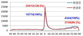
전술한 실시예와 비교예에 따라 제조된 광학 시트를 제작하기 전에 시뮬레이션하여 동일한 지점에서의 휘도를 계산하여 도 6에 그래프로 나타내었고 도 7a에 비교예의 이미지를 나타내었으며 도 7b에 실시예의 이미지를 나타내었다.The optical sheet manufactured according to the above-described embodiments and the comparative example is simulated before fabrication to calculate the brightness at the same point, and is shown in FIG. 6 as a graph. FIG. 7A shows an image of the comparative example. FIG. Respectively.
도 6, 도 7a 및 도 7b를 참조하면, 비교예의 광학 시트의 휘도를 100%로 보았을 때 실시예의 광학 시트는 126.5%의 휘도를 나타났다. 또한, 비교예의 광학 시트는 외곽부에서 휘도가 측정되어 손실광이 나타나나, 실시예의 광학 시트는 외곽부에서의 휘도가 비교예보다 적게 측정되는 것으로 나타났다.Referring to Figs. 6, 7A and 7B, when the luminance of the optical sheet of the comparative example is taken as 100%, the optical sheet of the embodiment shows a luminance of 126.5%. Further, in the optical sheet of the comparative example, the luminance was measured at the outer frame portion, and the lost light appeared, but the brightness of the optical sheet of the embodiment was measured at the outer frame portion less than that of Comparative Example.
광학 시트 제작 결과Optical sheet production result
전술한 실시예와 비교예에 따라 광학 시트를 제조하였다. 비교예의 프리즘 형상의 이미지를 도 8a에 나타내었고, 실시예의 프리즘 형상의 이미지를 도 8b에 나타내었다. 또한, 실시예와 비교예에 따라 제조된 광학 시트의 동일한 지점에서의 휘도를 측정하여 도 9에 그래프로 나타내었고 도 10a에 비교예의 이미지를 나타내었으며 도 10b에 실시예의 이미지를 나타내었다.An optical sheet was prepared in accordance with the above-described Examples and Comparative Examples. A prism-shaped image of the comparative example is shown in Fig. 8A, and a prism-shaped image of the embodiment is shown in Fig. 8B. In addition, the brightness of the optical sheet manufactured according to the examples and the comparative example was measured at the same point, and the graph of FIG. 9 was shown. FIG. 10A shows the image of the comparative example, and FIG. 10B shows the image of the embodiment.
도 9, 도 10a 및 도 10b를 참조하면, 비교예의 광학 시트의 휘도를 100%로 보았을 때 실시예의 광학 시트는 126.2%의 휘도를 나타내어, 시뮬레이션 결과와 매우 유사하게 나타났다. 또한, 비교예의 광학 시트는 외곽부에서 휘도가 측정되어 손실광이 나타나나, 실시예의 광학 시트는 외곽부에서의 휘도가 비교예보다 적게 측정되는 것으로 나타났다. 특히, 시뮬레이션 결과보다 비교예의 광학 시트에서 손실광이 많이 나타나는 것을 확인하였다.Referring to Figs. 9, 10A and 10B, when the luminance of the optical sheet of the comparative example is taken as 100%, the optical sheet of the embodiment shows a luminance of 126.2%, which is very similar to the simulation result. Further, in the optical sheet of the comparative example, the luminance was measured at the outer frame portion, and the lost light appeared, but the brightness of the optical sheet of the embodiment was measured at the outer frame portion less than that of Comparative Example. Particularly, it was confirmed that a lot of lost light appeared in the optical sheet of the comparative example than the simulation result.
상기와 같이, 본 발명의 일 실시예에 따른 광학 시트, 이를 포함하는 백라이트 유닛 및 액정표시장치는 고굴절률층과 저굴절률층을 포함하되 고굴절률층의 프리즘의 형상을 변경함으로써, 프리즘부의 피치를 줄이고 광 경로를 변경시켜 외부로 빠져나가는 손실광을 줄일 수 있는 효과가 있다. 따라서, 백라이트 유닛의 휘도를 향상시켜 표시품질이 우수한 액정표시장치를 제공할 수 있는 이점이 있다. As described above, the optical sheet according to an embodiment of the present invention, the backlight unit including the same, and the liquid crystal display device include a high refractive index layer and a low refractive index layer. By changing the shape of the prism of the high refractive index layer, It is possible to reduce the loss of light passing through to the outside by changing the optical path. Therefore, there is an advantage that a liquid crystal display device having improved display quality can be provided by improving the brightness of the backlight unit.
이상 첨부된 도면을 참조하여 본 발명의 실시 예를 설명하였지만, 상술한 본 발명의 기술적 구성은 본 발명이 속하는 기술 분야의 당업자가 본 발명의 그 기술적 사상이나 필수적 특징을 변경하지 않고서 다른 구체적인 형태로 실시될 수 있다는 것을 이해할 수 있을 것이다. 그러므로 이상에서 기술한 실시 예들은 모든 면에서 예시적인 것이며 한정적인 것이 아닌 것으로서 이해되어야 한다. 아울러, 본 발명의 범위는 상기 상세한 설명보다는 후술하는 특허청구범위에 의하여 나타내어진다. 또한, 특허청구범위의 의미 및 범위 그리고 그 등가 개념으로부터 도출되는 모든 변경 또는 변형된 형태가 본 발명의 범위에 포함되는 것으로 해석되어야 한다.
While the present invention has been described in connection with what is presently considered to be practical exemplary embodiments thereof, it is to be understood that the invention is not limited to the disclosed embodiments, but, on the contrary, It will be understood that the invention may be practiced. It is therefore to be understood that the embodiments described above are to be considered in all respects only as illustrative and not restrictive. In addition, the scope of the present invention is indicated by the following claims rather than the detailed description. Also, all changes or modifications derived from the meaning and scope of the claims and their equivalents should be construed as being included within the scope of the present invention.
210 : 베이스 필름 220 : 고굴절률층
221 : 프리즘부 225 : 입사면
225a : 제1 입사면 225b : 제2 입사면
226 : 반사면 230 : 저굴절률층210: base film 220: high refractive index layer
221: prism portion 225: incident surface
225a:
226: Reflecting surface 230: Low refractive index layer
Claims (7)
상기 베이스 필름 상에 복수의 프리즘부를 가지는 고굴절률층; 및
상기 고굴절률층 상에 위치하며, 상기 복수의 프리즘부를 덮되 상기 베이스 필름과 나란한 표면을 가지는 저굴절률층을 포함하며,
상기 프리즘부는 광이 입사되는 입사면과 입사된 광을 반사하는 반사면을 포함하되, 상기 입사면은 어느 일 지점에서 굴절되는 것을 특징으로 하는 광학 시트.
A base film;
A high refractive index layer having a plurality of prism portions on the base film; And
And a low refractive index layer disposed on the high refractive index layer and having a surface that covers the plurality of prism portions and is in parallel with the base film,
Wherein the prism portion includes an incident surface on which light is incident and a reflection surface that reflects incident light, wherein the incident surface is refracted at one point.
상기 복수의 프리즘부는 일 방향으로 연속적으로 연장된 것을 특징으로 하는 광학 시트.
The method according to claim 1,
Wherein the plurality of prism portions continuously extend in one direction.
상기 입사면은 상기 입사면이 굴절된 지점을 기준으로 상기 베이스 필름과 인접한 제1 입사면 및 상기 입사면과 상기 반사면이 만나는 꼭지점에 연결된 제2 입사면을 포함하는 것을 특징으로 하는 광학 시트.
The method according to claim 1,
Wherein the incident surface includes a first incident surface adjacent to the base film and a second incident surface connected to a vertex at which the incident surface and the reflection surface meet based on a point at which the incident surface is refracted.
상기 제1 입사면과 상기 베이스 필름의 표면이 이루는 각도는 90도 이하인 것을 특징으로 하는 광학 시트.
The method of claim 3,
Wherein an angle formed by the first incident surface and a surface of the base film is 90 degrees or less.
상기 제2 입사면과 상기 반사면이 이루는 각도는 상기 제1 입사면과 상기 제2 입사면이 이루는 각도보다 작은 것을 특징으로 하는 광학 시트.
The method of claim 3,
And the angle formed by the second incident surface and the reflecting surface is smaller than the angle formed by the first incident surface and the second incident surface.
상기 광원의 측면에 위치하는 도광판;
상기 도광판 하부에 위치하는 반사판; 및
상기 도광판 상에 위치하는 광학 시트를 포함하며,
상기 광학 시트는,
베이스 필름;
상기 베이스 필름 상에 복수의 프리즘부를 가지는 고굴절률층; 및
상기 고굴절률층 상에 위치하며, 상기 복수의 돌출부들을 덮되 상기 베이스 필름과 나란한 표면을 가지는 저굴절률층을 포함하며,
상기 프리즘부는 광이 입사되는 입사면과 입사된 광을 반사하는 반사면을 포함하되, 상기 입사면은 어느 일 지점에서 굴절되는 것을 특징으로 하는 백라이트 유닛.
Light source;
A light guide plate disposed on a side surface of the light source;
A reflection plate positioned below the light guide plate; And
And an optical sheet positioned on the light guide plate,
In the optical sheet,
A base film;
A high refractive index layer having a plurality of prism portions on the base film; And
And a low refractive index layer located on the high refractive index layer and covering the plurality of protrusions, the low refractive index layer having a surface parallel to the base film,
Wherein the prism portion includes an incident surface on which light is incident and a reflection surface that reflects incident light, wherein the incident surface is refracted at a certain point.
상기 광원의 측면에 위치하는 도광판;
상기 도광판 하부에 위치하는 반사판;
상기 도광판 상에 위치하는 광학 시트; 및
상기 광학 시트 상에 위치하는 액정패널을 포함하며,
상기 광학 시트는,
베이스 필름;
상기 베이스 필름 상에 복수의 프리즘부를 가지는 고굴절률층; 및
상기 고굴절률층 상에 위치하며, 상기 복수의 돌출부들을 덮되 상기 베이스 필름과 나란한 표면을 가지는 저굴절률층을 포함하며,
상기 프리즘부는 광이 입사되는 입사면과 입사된 광을 반사하는 반사면을 포함하되, 상기 입사면은 어느 일 지점에서 굴절되는 것을 특징으로 하는 액정표시장치.Light source;
A light guide plate disposed on a side surface of the light source;
A reflection plate positioned below the light guide plate;
An optical sheet positioned on the light guide plate; And
And a liquid crystal panel positioned on the optical sheet,
In the optical sheet,
A base film;
A high refractive index layer having a plurality of prism portions on the base film; And
And a low refractive index layer located on the high refractive index layer and covering the plurality of protrusions, the low refractive index layer having a surface parallel to the base film,
Wherein the prism portion includes an incident surface on which light is incident and a reflection surface that reflects incident light, wherein the incident surface is refracted at a certain point.
Priority Applications (3)
| Application Number | Priority Date | Filing Date | Title |
|---|---|---|---|
| KR20130104353A KR20150026044A (en) | 2013-08-30 | 2013-08-30 | Optical sheet, backlight unit and display device comprising the same |
| CN201310706323.8A CN104423089A (en) | 2013-08-30 | 2013-12-19 | Optical sheet and backlight unit and display device comprising the same |
| US14/137,684 US9618682B2 (en) | 2013-08-30 | 2013-12-20 | Optical sheet and backlight unit and display device comprising the same |
Applications Claiming Priority (1)
| Application Number | Priority Date | Filing Date | Title |
|---|---|---|---|
| KR20130104353A KR20150026044A (en) | 2013-08-30 | 2013-08-30 | Optical sheet, backlight unit and display device comprising the same |
Publications (1)
| Publication Number | Publication Date |
|---|---|
| KR20150026044A true KR20150026044A (en) | 2015-03-11 |
Family
ID=52582766
Family Applications (1)
| Application Number | Title | Priority Date | Filing Date |
|---|---|---|---|
| KR20130104353A Ceased KR20150026044A (en) | 2013-08-30 | 2013-08-30 | Optical sheet, backlight unit and display device comprising the same |
Country Status (3)
| Country | Link |
|---|---|
| US (1) | US9618682B2 (en) |
| KR (1) | KR20150026044A (en) |
| CN (1) | CN104423089A (en) |
Cited By (3)
| Publication number | Priority date | Publication date | Assignee | Title |
|---|---|---|---|---|
| US9964686B2 (en) | 2016-04-19 | 2018-05-08 | Samsung Display Co., Ltd. | Display apparatus |
| KR20210115949A (en) * | 2020-03-17 | 2021-09-27 | 주식회사 엘엠에스 | Optical film for fingerprinting recognition |
| US11288486B2 (en) | 2019-06-12 | 2022-03-29 | Lms Co., Ltd. | Fingerprint recognition optical film, and backlight unit and liquid crystal display device comprising the film optical |
Families Citing this family (25)
| Publication number | Priority date | Publication date | Assignee | Title |
|---|---|---|---|---|
| SE533704C2 (en) | 2008-12-05 | 2010-12-07 | Flatfrog Lab Ab | Touch sensitive apparatus and method for operating the same |
| JP6391387B2 (en) * | 2014-09-24 | 2018-09-19 | キヤノン株式会社 | Light guide unit, illumination device using the same, and image reading device |
| WO2016122385A1 (en) | 2015-01-28 | 2016-08-04 | Flatfrog Laboratories Ab | Dynamic touch quarantine frames |
| EP3537269A1 (en) | 2015-02-09 | 2019-09-11 | FlatFrog Laboratories AB | Optical touch system |
| WO2016140612A1 (en) * | 2015-03-02 | 2016-09-09 | Flatfrog Laboratories Ab | Optical component for light coupling |
| KR101730822B1 (en) * | 2015-06-22 | 2017-05-11 | 주식회사 엘엠에스 | Optical Sheet Module And Back Light Unit Using The Same |
| JP2017049326A (en) * | 2015-08-31 | 2017-03-09 | 株式会社ジャパンディスプレイ | Display device |
| KR20170039814A (en) * | 2015-10-01 | 2017-04-12 | 삼성디스플레이 주식회사 | Optical component and display device having the same |
| KR102400705B1 (en) | 2015-12-09 | 2022-05-23 | 플라트프로그 라보라토리즈 에이비 | Improved stylus identification |
| CN110100226A (en) | 2016-11-24 | 2019-08-06 | 平蛙实验室股份公司 | The Automatic Optimal of touch signal |
| CN119847372A (en) | 2016-12-07 | 2025-04-18 | 平蛙实验室股份公司 | Touch sensing device |
| CN106707621A (en) | 2017-01-17 | 2017-05-24 | 京东方科技集团股份有限公司 | Backlight module, display panel comprising same and electronic device |
| CN116679845A (en) | 2017-02-06 | 2023-09-01 | 平蛙实验室股份公司 | touch sensing device |
| US20180275830A1 (en) | 2017-03-22 | 2018-09-27 | Flatfrog Laboratories Ab | Object characterisation for touch displays |
| WO2018182476A1 (en) | 2017-03-28 | 2018-10-04 | Flatfrog Laboratories Ab | Touch sensing apparatus and method for assembly |
| CN117311543A (en) | 2017-09-01 | 2023-12-29 | 平蛙实验室股份公司 | Touch sensing device |
| JP2019125543A (en) * | 2018-01-19 | 2019-07-25 | シャープ株式会社 | Lighting device and display device |
| WO2019172826A1 (en) | 2018-03-05 | 2019-09-12 | Flatfrog Laboratories Ab | Improved touch-sensing apparatus |
| CN112889016A (en) | 2018-10-20 | 2021-06-01 | 平蛙实验室股份公司 | Frame for touch sensitive device and tool therefor |
| WO2020153890A1 (en) | 2019-01-25 | 2020-07-30 | Flatfrog Laboratories Ab | A videoconferencing terminal and method of operating the same |
| EP4066089B1 (en) | 2019-11-25 | 2024-09-25 | FlatFrog Laboratories AB | A touch-sensing apparatus |
| CN111045256B (en) * | 2020-01-06 | 2023-03-10 | 京东方科技集团股份有限公司 | Backlight module and display device |
| US12282653B2 (en) | 2020-02-08 | 2025-04-22 | Flatfrog Laboratories Ab | Touch apparatus with low latency interactions |
| US11893189B2 (en) | 2020-02-10 | 2024-02-06 | Flatfrog Laboratories Ab | Touch-sensing apparatus |
| CN115373066B (en) * | 2022-08-25 | 2025-06-20 | 武汉华星光电技术有限公司 | Backlight module and display device |
Family Cites Families (7)
| Publication number | Priority date | Publication date | Assignee | Title |
|---|---|---|---|---|
| CN1187639C (en) * | 2001-07-13 | 2005-02-02 | 兴隆发电子股份有限公司 | Manufacturing method of light guide plate and mold thereof |
| KR100447801B1 (en) * | 2003-07-10 | 2004-09-08 | 주식회사 엘지에스 | Optical film for Back-light unit and Manufacturing Method those |
| CN1816719B (en) * | 2003-07-15 | 2011-08-10 | 三菱丽阳株式会社 | Light source device and light deflection element |
| US7440045B2 (en) * | 2004-06-11 | 2008-10-21 | Hannstar Display Corporation | Flat panel display having a brightness enhancement diffuser plate with two diffusing layers |
| US8558966B2 (en) * | 2008-06-26 | 2013-10-15 | Lg Display Co., Ltd. | Liquid crystal display device including back light having improved light concentration efficiency |
| KR101336039B1 (en) * | 2008-06-26 | 2013-12-04 | 엘지디스플레이 주식회사 | Liquid crystal display device |
| KR100978078B1 (en) * | 2008-08-26 | 2010-08-26 | 삼성전자주식회사 | Prism sheet and liquid crystal display device having same |
-
2013
- 2013-08-30 KR KR20130104353A patent/KR20150026044A/en not_active Ceased
- 2013-12-19 CN CN201310706323.8A patent/CN104423089A/en active Pending
- 2013-12-20 US US14/137,684 patent/US9618682B2/en active Active
Cited By (3)
| Publication number | Priority date | Publication date | Assignee | Title |
|---|---|---|---|---|
| US9964686B2 (en) | 2016-04-19 | 2018-05-08 | Samsung Display Co., Ltd. | Display apparatus |
| US11288486B2 (en) | 2019-06-12 | 2022-03-29 | Lms Co., Ltd. | Fingerprint recognition optical film, and backlight unit and liquid crystal display device comprising the film optical |
| KR20210115949A (en) * | 2020-03-17 | 2021-09-27 | 주식회사 엘엠에스 | Optical film for fingerprinting recognition |
Also Published As
| Publication number | Publication date |
|---|---|
| CN104423089A (en) | 2015-03-18 |
| US20150062493A1 (en) | 2015-03-05 |
| US9618682B2 (en) | 2017-04-11 |
Similar Documents
| Publication | Publication Date | Title |
|---|---|---|
| KR20150026044A (en) | Optical sheet, backlight unit and display device comprising the same | |
| US9971081B1 (en) | Lighting device and display device | |
| US20170269285A1 (en) | Illumination device and display device | |
| KR100978078B1 (en) | Prism sheet and liquid crystal display device having same | |
| US10317610B2 (en) | Illumination device and display device | |
| CN102003658A (en) | Optical sheet, backlight unit and liquid crystal display device having the same and method of fabricating optical sheet | |
| US7859612B2 (en) | Light concentrating sheet, backlight unit including the light concentrating sheet and liquid crystal display module including the backlight unit | |
| US20150138487A1 (en) | Optical member, illumination device, and display device | |
| US9477117B2 (en) | Optical lens module and backlight unit | |
| EP3264146A1 (en) | Laminated optical member, lighting device, display device and television receiver | |
| US9921360B2 (en) | Illumination device and display device | |
| CN106104141A (en) | Lighting device and display device | |
| KR20110076373A (en) | LS and liquid crystal display including the same | |
| US20150146132A1 (en) | Surface light source device, display device, and lighting device | |
| KR20140072635A (en) | Liquid crystal display device | |
| WO2014050651A1 (en) | Optical member, illumination device, and display device | |
| US20160124270A1 (en) | Illumination device, display device, and tv receiver | |
| US20060109395A1 (en) | Area light source device and liquid crystal display device including the same | |
| US20140320783A1 (en) | Condensing sheet, backlight unit and liquid crystal display device using the same | |
| KR100989046B1 (en) | Optical sheet, backlight unit and liquid crystal display including the same | |
| KR100939740B1 (en) | Backlight unit and liquid crystal display including the same | |
| KR101746675B1 (en) | Multi-light guide sheet and liquid crystal display device including the same | |
| KR102053442B1 (en) | Optical sheet and liquid crystal display device comprising the same | |
| KR101749750B1 (en) | Backlight Unit And Liquid Crystal Diplay | |
| KR101816314B1 (en) | Backlgiht unit and liquid crystal display device the same |
Legal Events
| Date | Code | Title | Description |
|---|---|---|---|
| PA0109 | Patent application |
Patent event code: PA01091R01D Comment text: Patent Application Patent event date: 20130830 |
|
| PG1501 | Laying open of application | ||
| A201 | Request for examination | ||
| PA0201 | Request for examination |
Patent event code: PA02012R01D Patent event date: 20180627 Comment text: Request for Examination of Application Patent event code: PA02011R01I Patent event date: 20130830 Comment text: Patent Application |
|
| E902 | Notification of reason for refusal | ||
| PE0902 | Notice of grounds for rejection |
Comment text: Notification of reason for refusal Patent event date: 20190618 Patent event code: PE09021S01D |
|
| AMND | Amendment | ||
| E601 | Decision to refuse application | ||
| PE0601 | Decision on rejection of patent |
Patent event date: 20191227 Comment text: Decision to Refuse Application Patent event code: PE06012S01D Patent event date: 20190618 Comment text: Notification of reason for refusal Patent event code: PE06011S01I |
|
| X091 | Application refused [patent] | ||
| AMND | Amendment | ||
| PX0901 | Re-examination |
Patent event code: PX09011S01I Patent event date: 20191227 Comment text: Decision to Refuse Application Patent event code: PX09012R01I Patent event date: 20190809 Comment text: Amendment to Specification, etc. |
|
| PX0601 | Decision of rejection after re-examination |
Comment text: Decision to Refuse Application Patent event code: PX06014S01D Patent event date: 20200210 Comment text: Amendment to Specification, etc. Patent event code: PX06012R01I Patent event date: 20200128 Comment text: Decision to Refuse Application Patent event code: PX06011S01I Patent event date: 20191227 Comment text: Amendment to Specification, etc. Patent event code: PX06012R01I Patent event date: 20190809 Comment text: Notification of reason for refusal Patent event code: PX06013S01I Patent event date: 20190618 |