KR20150003667A - Light emitting display apparatus and driving method thereof - Google Patents
Light emitting display apparatus and driving method thereof Download PDFInfo
- Publication number
- KR20150003667A KR20150003667A KR20140073762A KR20140073762A KR20150003667A KR 20150003667 A KR20150003667 A KR 20150003667A KR 20140073762 A KR20140073762 A KR 20140073762A KR 20140073762 A KR20140073762 A KR 20140073762A KR 20150003667 A KR20150003667 A KR 20150003667A
- Authority
- KR
- South Korea
- Prior art keywords
- transistor
- voltage
- light emitting
- charging
- turned
- Prior art date
- Legal status (The legal status is an assumption and is not a legal conclusion. Google has not performed a legal analysis and makes no representation as to the accuracy of the status listed.)
- Granted
Links
- 238000000034 method Methods 0.000 title claims abstract description 38
- 239000003990 capacitor Substances 0.000 claims abstract description 43
- 230000003071 parasitic effect Effects 0.000 claims description 5
- 230000008878 coupling Effects 0.000 claims description 3
- 238000010168 coupling process Methods 0.000 claims description 3
- 238000005859 coupling reaction Methods 0.000 claims description 3
- 230000000750 progressive effect Effects 0.000 description 15
- 238000010586 diagram Methods 0.000 description 14
- 230000008859 change Effects 0.000 description 13
- 239000011521 glass Substances 0.000 description 7
- 230000000694 effects Effects 0.000 description 3
- 239000011159 matrix material Substances 0.000 description 3
- 230000001052 transient effect Effects 0.000 description 3
- 230000006866 deterioration Effects 0.000 description 2
- 238000004519 manufacturing process Methods 0.000 description 2
- 239000004065 semiconductor Substances 0.000 description 2
- 229910021417 amorphous silicon Inorganic materials 0.000 description 1
- 238000006243 chemical reaction Methods 0.000 description 1
- 230000003111 delayed effect Effects 0.000 description 1
- 230000006870 function Effects 0.000 description 1
- 239000004973 liquid crystal related substance Substances 0.000 description 1
- 230000001360 synchronised effect Effects 0.000 description 1
- 239000010409 thin film Substances 0.000 description 1
- 238000002834 transmittance Methods 0.000 description 1
Images


Classifications
-
- G—PHYSICS
- G09—EDUCATION; CRYPTOGRAPHY; DISPLAY; ADVERTISING; SEALS
- G09G—ARRANGEMENTS OR CIRCUITS FOR CONTROL OF INDICATING DEVICES USING STATIC MEANS TO PRESENT VARIABLE INFORMATION
- G09G3/00—Control arrangements or circuits, of interest only in connection with visual indicators other than cathode-ray tubes
- G09G3/20—Control arrangements or circuits, of interest only in connection with visual indicators other than cathode-ray tubes for presentation of an assembly of a number of characters, e.g. a page, by composing the assembly by combination of individual elements arranged in a matrix no fixed position being assigned to or needed to be assigned to the individual characters or partial characters
- G09G3/22—Control arrangements or circuits, of interest only in connection with visual indicators other than cathode-ray tubes for presentation of an assembly of a number of characters, e.g. a page, by composing the assembly by combination of individual elements arranged in a matrix no fixed position being assigned to or needed to be assigned to the individual characters or partial characters using controlled light sources
- G09G3/30—Control arrangements or circuits, of interest only in connection with visual indicators other than cathode-ray tubes for presentation of an assembly of a number of characters, e.g. a page, by composing the assembly by combination of individual elements arranged in a matrix no fixed position being assigned to or needed to be assigned to the individual characters or partial characters using controlled light sources using electroluminescent panels
- G09G3/32—Control arrangements or circuits, of interest only in connection with visual indicators other than cathode-ray tubes for presentation of an assembly of a number of characters, e.g. a page, by composing the assembly by combination of individual elements arranged in a matrix no fixed position being assigned to or needed to be assigned to the individual characters or partial characters using controlled light sources using electroluminescent panels semiconductive, e.g. using light-emitting diodes [LED]
- G09G3/3208—Control arrangements or circuits, of interest only in connection with visual indicators other than cathode-ray tubes for presentation of an assembly of a number of characters, e.g. a page, by composing the assembly by combination of individual elements arranged in a matrix no fixed position being assigned to or needed to be assigned to the individual characters or partial characters using controlled light sources using electroluminescent panels semiconductive, e.g. using light-emitting diodes [LED] organic, e.g. using organic light-emitting diodes [OLED]
- G09G3/3225—Control arrangements or circuits, of interest only in connection with visual indicators other than cathode-ray tubes for presentation of an assembly of a number of characters, e.g. a page, by composing the assembly by combination of individual elements arranged in a matrix no fixed position being assigned to or needed to be assigned to the individual characters or partial characters using controlled light sources using electroluminescent panels semiconductive, e.g. using light-emitting diodes [LED] organic, e.g. using organic light-emitting diodes [OLED] using an active matrix
- G09G3/3258—Control arrangements or circuits, of interest only in connection with visual indicators other than cathode-ray tubes for presentation of an assembly of a number of characters, e.g. a page, by composing the assembly by combination of individual elements arranged in a matrix no fixed position being assigned to or needed to be assigned to the individual characters or partial characters using controlled light sources using electroluminescent panels semiconductive, e.g. using light-emitting diodes [LED] organic, e.g. using organic light-emitting diodes [OLED] using an active matrix with pixel circuitry controlling the voltage across the light-emitting element
-
- G—PHYSICS
- G09—EDUCATION; CRYPTOGRAPHY; DISPLAY; ADVERTISING; SEALS
- G09G—ARRANGEMENTS OR CIRCUITS FOR CONTROL OF INDICATING DEVICES USING STATIC MEANS TO PRESENT VARIABLE INFORMATION
- G09G3/00—Control arrangements or circuits, of interest only in connection with visual indicators other than cathode-ray tubes
- G09G3/20—Control arrangements or circuits, of interest only in connection with visual indicators other than cathode-ray tubes for presentation of an assembly of a number of characters, e.g. a page, by composing the assembly by combination of individual elements arranged in a matrix no fixed position being assigned to or needed to be assigned to the individual characters or partial characters
- G09G3/22—Control arrangements or circuits, of interest only in connection with visual indicators other than cathode-ray tubes for presentation of an assembly of a number of characters, e.g. a page, by composing the assembly by combination of individual elements arranged in a matrix no fixed position being assigned to or needed to be assigned to the individual characters or partial characters using controlled light sources
- G09G3/30—Control arrangements or circuits, of interest only in connection with visual indicators other than cathode-ray tubes for presentation of an assembly of a number of characters, e.g. a page, by composing the assembly by combination of individual elements arranged in a matrix no fixed position being assigned to or needed to be assigned to the individual characters or partial characters using controlled light sources using electroluminescent panels
- G09G3/32—Control arrangements or circuits, of interest only in connection with visual indicators other than cathode-ray tubes for presentation of an assembly of a number of characters, e.g. a page, by composing the assembly by combination of individual elements arranged in a matrix no fixed position being assigned to or needed to be assigned to the individual characters or partial characters using controlled light sources using electroluminescent panels semiconductive, e.g. using light-emitting diodes [LED]
- G09G3/3208—Control arrangements or circuits, of interest only in connection with visual indicators other than cathode-ray tubes for presentation of an assembly of a number of characters, e.g. a page, by composing the assembly by combination of individual elements arranged in a matrix no fixed position being assigned to or needed to be assigned to the individual characters or partial characters using controlled light sources using electroluminescent panels semiconductive, e.g. using light-emitting diodes [LED] organic, e.g. using organic light-emitting diodes [OLED]
- G09G3/3225—Control arrangements or circuits, of interest only in connection with visual indicators other than cathode-ray tubes for presentation of an assembly of a number of characters, e.g. a page, by composing the assembly by combination of individual elements arranged in a matrix no fixed position being assigned to or needed to be assigned to the individual characters or partial characters using controlled light sources using electroluminescent panels semiconductive, e.g. using light-emitting diodes [LED] organic, e.g. using organic light-emitting diodes [OLED] using an active matrix
- G09G3/3233—Control arrangements or circuits, of interest only in connection with visual indicators other than cathode-ray tubes for presentation of an assembly of a number of characters, e.g. a page, by composing the assembly by combination of individual elements arranged in a matrix no fixed position being assigned to or needed to be assigned to the individual characters or partial characters using controlled light sources using electroluminescent panels semiconductive, e.g. using light-emitting diodes [LED] organic, e.g. using organic light-emitting diodes [OLED] using an active matrix with pixel circuitry controlling the current through the light-emitting element
-
- G—PHYSICS
- G09—EDUCATION; CRYPTOGRAPHY; DISPLAY; ADVERTISING; SEALS
- G09G—ARRANGEMENTS OR CIRCUITS FOR CONTROL OF INDICATING DEVICES USING STATIC MEANS TO PRESENT VARIABLE INFORMATION
- G09G3/00—Control arrangements or circuits, of interest only in connection with visual indicators other than cathode-ray tubes
- G09G3/20—Control arrangements or circuits, of interest only in connection with visual indicators other than cathode-ray tubes for presentation of an assembly of a number of characters, e.g. a page, by composing the assembly by combination of individual elements arranged in a matrix no fixed position being assigned to or needed to be assigned to the individual characters or partial characters
- G09G3/2007—Display of intermediate tones
-
- G—PHYSICS
- G09—EDUCATION; CRYPTOGRAPHY; DISPLAY; ADVERTISING; SEALS
- G09G—ARRANGEMENTS OR CIRCUITS FOR CONTROL OF INDICATING DEVICES USING STATIC MEANS TO PRESENT VARIABLE INFORMATION
- G09G3/00—Control arrangements or circuits, of interest only in connection with visual indicators other than cathode-ray tubes
- G09G3/20—Control arrangements or circuits, of interest only in connection with visual indicators other than cathode-ray tubes for presentation of an assembly of a number of characters, e.g. a page, by composing the assembly by combination of individual elements arranged in a matrix no fixed position being assigned to or needed to be assigned to the individual characters or partial characters
- G09G3/22—Control arrangements or circuits, of interest only in connection with visual indicators other than cathode-ray tubes for presentation of an assembly of a number of characters, e.g. a page, by composing the assembly by combination of individual elements arranged in a matrix no fixed position being assigned to or needed to be assigned to the individual characters or partial characters using controlled light sources
- G09G3/30—Control arrangements or circuits, of interest only in connection with visual indicators other than cathode-ray tubes for presentation of an assembly of a number of characters, e.g. a page, by composing the assembly by combination of individual elements arranged in a matrix no fixed position being assigned to or needed to be assigned to the individual characters or partial characters using controlled light sources using electroluminescent panels
- G09G3/32—Control arrangements or circuits, of interest only in connection with visual indicators other than cathode-ray tubes for presentation of an assembly of a number of characters, e.g. a page, by composing the assembly by combination of individual elements arranged in a matrix no fixed position being assigned to or needed to be assigned to the individual characters or partial characters using controlled light sources using electroluminescent panels semiconductive, e.g. using light-emitting diodes [LED]
- G09G3/3208—Control arrangements or circuits, of interest only in connection with visual indicators other than cathode-ray tubes for presentation of an assembly of a number of characters, e.g. a page, by composing the assembly by combination of individual elements arranged in a matrix no fixed position being assigned to or needed to be assigned to the individual characters or partial characters using controlled light sources using electroluminescent panels semiconductive, e.g. using light-emitting diodes [LED] organic, e.g. using organic light-emitting diodes [OLED]
- G09G3/3275—Details of drivers for data electrodes
- G09G3/3291—Details of drivers for data electrodes in which the data driver supplies a variable data voltage for setting the current through, or the voltage across, the light-emitting elements
-
- G—PHYSICS
- G09—EDUCATION; CRYPTOGRAPHY; DISPLAY; ADVERTISING; SEALS
- G09G—ARRANGEMENTS OR CIRCUITS FOR CONTROL OF INDICATING DEVICES USING STATIC MEANS TO PRESENT VARIABLE INFORMATION
- G09G2300/00—Aspects of the constitution of display devices
- G09G2300/04—Structural and physical details of display devices
- G09G2300/0421—Structural details of the set of electrodes
- G09G2300/043—Compensation electrodes or other additional electrodes in matrix displays related to distortions or compensation signals, e.g. for modifying TFT threshold voltage in column driver
-
- G—PHYSICS
- G09—EDUCATION; CRYPTOGRAPHY; DISPLAY; ADVERTISING; SEALS
- G09G—ARRANGEMENTS OR CIRCUITS FOR CONTROL OF INDICATING DEVICES USING STATIC MEANS TO PRESENT VARIABLE INFORMATION
- G09G2300/00—Aspects of the constitution of display devices
- G09G2300/08—Active matrix structure, i.e. with use of active elements, inclusive of non-linear two terminal elements, in the pixels together with light emitting or modulating elements
- G09G2300/0809—Several active elements per pixel in active matrix panels
- G09G2300/0819—Several active elements per pixel in active matrix panels used for counteracting undesired variations, e.g. feedback or autozeroing
-
- G—PHYSICS
- G09—EDUCATION; CRYPTOGRAPHY; DISPLAY; ADVERTISING; SEALS
- G09G—ARRANGEMENTS OR CIRCUITS FOR CONTROL OF INDICATING DEVICES USING STATIC MEANS TO PRESENT VARIABLE INFORMATION
- G09G2300/00—Aspects of the constitution of display devices
- G09G2300/08—Active matrix structure, i.e. with use of active elements, inclusive of non-linear two terminal elements, in the pixels together with light emitting or modulating elements
- G09G2300/0809—Several active elements per pixel in active matrix panels
- G09G2300/0842—Several active elements per pixel in active matrix panels forming a memory circuit, e.g. a dynamic memory with one capacitor
-
- G—PHYSICS
- G09—EDUCATION; CRYPTOGRAPHY; DISPLAY; ADVERTISING; SEALS
- G09G—ARRANGEMENTS OR CIRCUITS FOR CONTROL OF INDICATING DEVICES USING STATIC MEANS TO PRESENT VARIABLE INFORMATION
- G09G2310/00—Command of the display device
- G09G2310/02—Addressing, scanning or driving the display screen or processing steps related thereto
- G09G2310/0262—The addressing of the pixel, in a display other than an active matrix LCD, involving the control of two or more scan electrodes or two or more data electrodes, e.g. pixel voltage dependent on signals of two data electrodes
-
- G—PHYSICS
- G09—EDUCATION; CRYPTOGRAPHY; DISPLAY; ADVERTISING; SEALS
- G09G—ARRANGEMENTS OR CIRCUITS FOR CONTROL OF INDICATING DEVICES USING STATIC MEANS TO PRESENT VARIABLE INFORMATION
- G09G2320/00—Control of display operating conditions
- G09G2320/04—Maintaining the quality of display appearance
- G09G2320/043—Preventing or counteracting the effects of ageing
- G09G2320/045—Compensation of drifts in the characteristics of light emitting or modulating elements
Landscapes
- Engineering & Computer Science (AREA)
- Physics & Mathematics (AREA)
- Computer Hardware Design (AREA)
- General Physics & Mathematics (AREA)
- Theoretical Computer Science (AREA)
- Control Of El Displays (AREA)
- Control Of Indicators Other Than Cathode Ray Tubes (AREA)
- Chemical & Material Sciences (AREA)
- Crystallography & Structural Chemistry (AREA)
- Electroluminescent Light Sources (AREA)
Abstract
표시 장치의 구동 방법은 용량 소자에 초기화 전압을 충전하는 단계, 용량 소자에 계조 데이터 전압과 제1 트랜지스터의 문턱 전압으로 결정되는 제1 데이터 전압을 충전하는 단계, 및 용량 소자에 충전된 제1 데이터 전압에 대응하는 전류가 발광 소자에 공급되어 발광 소자가 발광하는 단계를 포함한다.A method of driving a display device includes charging a capacitor element with an initialization voltage, charging a capacitor element with a first data voltage determined by a gradation data voltage and a threshold voltage of the first transistor, And a current corresponding to the voltage is supplied to the light emitting element so that the light emitting element emits light.
Description
본 발명은 발광 표시 장치 및 그 구동 방법에 관한 발명이다.The present invention relates to a light emitting display and a driving method thereof.
최근, CRT 디스플레이(Cathode Ray Tube display)를 대체하는 표시 장치로서, 액정 디스플레이(Liquid Crystal Display Device:LCD) 및 유기 EL 표시 장치가 사용되고 있다. 특히 유기 EL 표시 장치는 저 소비 전력 및 박형 디스플레이로서 매우 주목을 받고 있다. 유기 EL 표시 장치에서, 화소의 유기 EL 소자로 흐르는 전류에 의해 발광 휘도가 변화된다. 그러나, 액티브 매트릭스 패널로 사용하는 박막 트랜지스터(TFT) 소자의 특성 변화(TFT 문턱 전압(VTH) 변화)에 의해, 화소마다 유기 EL 소자로 흐르는 전류가 달라질 수 있다. 이러한 경우, 화소마다 휘도가 변화되어 표시 품질이 저하될 수 있다.2. Description of the Related Art In recent years, liquid crystal displays (LCDs) and organic EL display devices have been used as display devices to replace CRT displays (Cathode Ray Tube displays). Particularly, organic EL display devices are attracting much attention as low power consumption and thin display. In the organic EL display device, the light emission luminance is changed by the current flowing to the organic EL element of the pixel. However, the current flowing to the organic EL element for each pixel can be changed by a change in characteristics (change in the TFT threshold voltage VTH) of the thin film transistor (TFT) element used in the active matrix panel. In such a case, the luminance may change for each pixel, and the display quality may deteriorate.
구동 트랜지스터의 특성 변화에 따른 표시 품질의 저하를 억제하기 위해, 유기 EL 소자로 흐르는 전류를 일정하게 하는 정전류 회로를 이용하여 구동 트랜지스터의 VTH (문턱 전압) 변화를 억제하기 위한 기술로서 VTH 보상 기술이 개발되어 있다.As a technique for suppressing the VTH (threshold voltage) change of the driving transistor by using a constant current circuit which makes the current flowing to the organic EL element constant, in order to suppress the deterioration of the display quality due to the characteristic change of the driving transistor, Has been developed.
특허 문헌1에서는, 각 화소는 4개의 트랜지스터, 2개의 용량 소자, 및 발광 소자를 포함한다. 화소들은 초기화 기간, VTH 보상 기간, 데이터 프로그램 기간, 및 발광 기간으로 구분되어 구동된다.In
특허 문헌2에서는, 각 화소는 3개의 트랜지스터, 2개의 용량 소자를 포함한다. 화소들은 초기화 기간, VTH 보상 기간, 데이터 프로그램 기간, 및 발광 기간으로 구분되어 구동된다.In
[선행기술문헌][Prior Art Literature]
[특허문헌][Patent Literature]
[특허 문헌1]일본국 특허 공개 제 2010-145579호 공보[Patent Document 1] Japanese Patent Application Laid-Open No. 2010-145579
[특허 문헌2]일본국 특허 공개 제 2011-034039호 공보[Patent Document 2] Japanese Patent Application Laid-Open No. 2011-034039
특허 문헌1 및 특허 문헌2의 화소 회로에서, VTH 보상과 데이터 프로그램 동작이 동시에 수행될 수 없다. 따라서, VTH 보상 동작이 먼저 수행되어 구동 트랜지스터의 VTH 전압이 충전되고, 그 후에 다른 용량 소자와의 용량 결합에 의해 데이터 프로그램 동작이 수행된다. 따라서, 화소 회로에 2개의 용량 소자가 요구된다. 화소 레이 아웃에서 용량 소자가 차지하는 비율이 크기 때문에, 이러한 경우, 고해상도의 구현이 어려워진다. In the pixel circuits of
또한, 특허 문헌1 및 특허 문헌2의 화소 회로에서, 프로그레시브(progressive) 구동(또는 순차 구동)과 사이멀테니어스(simultaneous) 구동(또는 동시 구동)이 상호 전환될 수 없다. 프로그레시브 구동에서 높은 발광 듀티가 얻어질 수 있지만, 셔터 안경을 사용하는 3차원 표시(3D)가 수행될 수 없다. 한편, 사이멀테니어스 구동에서, 셔터 안경을 사용한 3차원 표시(3D)가 수행될 수 있지만, 선 순차적으로 발광/비발광이 제어될 수 없기 때문에, 낮은 발광 듀티로 발광이 제어되어야 한다. 발광 듀티가 저하되면, 발광 소자에 높은 피크 전류가 제공되어야 하므로, 발광 소자의 수명이 떨어질 수 있다. Further, in the pixel circuits of
본 발명의 목적은, 용량 소자의 소자 수를 저감시킴으로써, 고해상도를 구현할 수 있는 발광 표시 장치 및 그 구동 방법을 제공하는데 있다.An object of the present invention is to provide a light emitting display device and a driving method thereof that can realize high resolution by reducing the number of elements of a capacitor element.
본 발명의 실시 예에 따른 발광 표시 장치의 구동 방법은 공급받은 전류에 의해 계조가 결정되는 발광 소자, 게이트 전극에 공급되는 전압에 따라서 상기 발광 소자로 공급되는 상기 전류의 크기를 제어하고, 제1 단자가 상기 발광 소자의 한쪽의 단자에 접속된 제1 트랜지스터, 상기 제1 트랜지스터의 상기 게이트 전극과 제1 전원 사이에 접속된 제2 트랜지스터, 제1 단자가 상기 제1 트랜지스터의 상기 게이트 전극에 접속되고, 제2 단자가 용량 소자를 통해 상기 제1 트랜지스터의 제2 단자에 접속된 제3 트랜지스터, 상기 제1 트랜지스터의 상기 제2 단자와 제2 전원 사이에 접속된 제 4 트랜지스터, 및 상기 제3 트랜지스터의 제2 단자와 초기화 전압 및 계조 데이터 전압이 공급되는 신호선 사이에 접속된 제5 트랜지스터를 각각 갖는 화소 회로들이 매트릭스 형상으로 배치된 발광 표시 장치의 구동 방법으로서, 상기 용량 소자에 상기 초기화 전압을 충전하는 단계, 상기 용량 소자에 상기 계조 데이터 전압과 상기 제1 트랜지스터의 문턱 전압으로 결정되는 제1 데이터 전압을 충전하는 단계, 및 상기 용량 소자에 충전된 상기 제1 데이터 전압에 대응하는 전류가 상기 발광 소자에 공급되어 상기 발광 소자가 발광하는 단계를 포함한다.A method of driving a light emitting display according to an embodiment of the present invention includes controlling a magnitude of the current supplied to a light emitting element according to a voltage supplied to a gate electrode, A first transistor having a terminal connected to one terminal of the light emitting element, a second transistor connected between the gate electrode of the first transistor and the first power supply, a first terminal connected to the gate electrode of the first transistor A fourth transistor connected between the second terminal of the first transistor and the second power supply, and a third transistor connected between the second terminal of the first transistor and the third terminal of the third transistor, The pixel circuits each having the fifth transistor connected between the second terminal of the transistor and the signal line to which the initialization voltage and the gradation data voltage are supplied, A step of charging the capacitor with the initialization voltage; and a step of charging the capacitor with the first data voltage determined by the gradation data voltage and the threshold voltage of the first transistor And a current corresponding to the first data voltage charged in the capacitive element is supplied to the light emitting element so that the light emitting element emits light.
상기 제1 데이터 전압을 충전하는 단계 전에 상기 용량 소자에 상기 문턱 전압으로 결정되는 전압을 충전하는 단계를 더 포함한다.And charging the capacitor to a voltage determined as the threshold voltage before charging the first data voltage.
상기 초기화 전압을 충전하는 단계와 상기 발광 소자가 발광하는 단계 사이에서 상기 문턱 전압으로 결정되는 전압을 충전하는 단계가 복수회 수행된다.The step of charging the voltage determined as the threshold voltage between the step of charging the initialization voltage and the step of emitting the light emitting element is performed a plurality of times.
상기 초기화 전압을 충전하는 단계에서, 상기 제3 트랜지스터를 오프 시키키고, 상기 제3 트랜지스터를 오프 시킨 이후에, 상기 제2 트랜지스터를 온 시키고, 상기 제1 트랜지스터의 상기 게이트 전극에 상기 제1 트랜지스터를 오프 시키는 상기 제1 전원의 전압을 공급하고, 상기 제4 트랜지스터 및 상기 제 5 트랜지스터를 온 시켜 상기 용량 소자의 양 단자에 상기 제2 전원의 전압 및 상기 신호선의 상기 초기화 전압을 공급한다.Wherein the step of charging the initialization voltage turns off the third transistor and turns off the third transistor so that the second transistor is turned on and the first transistor is connected to the gate electrode of the first transistor And turns on the fourth transistor and the fifth transistor to supply the voltage of the second power source and the initialization voltage of the signal line to both terminals of the capacitive element.
상기 발광 소자의 다른 쪽의 단자는 제3 전원에 접속되고, 상기 초기화 전압을 충전하는 단계에서, 상기 제3 트랜지스터를 오프시키고, 상기 제3 트랜지스터를 오프시킨 이후에, 상기 제5 트랜지스터를 온 시키고, 상기 용량 소자의 한쪽의 단자에 상기 제3 전원의 전압을 공급하고, 상기 제2 트랜지스터를 온 시키고, 상기 제1 트랜지스터의 게이트 전극에 상기 제1 전원의 전압을 공급하고, 상기 제3 전원의 전압을 변화시키고, 상기 발광 소자의 용량 성분의 용량 결합에 의해 상기 제1 트랜지스터가 온 되고, 상기 용량 소자에 상기 초기화 전압을 충전한다.The other terminal of the light emitting element is connected to the third power supply, and in the step of charging the initialization voltage, the third transistor is turned off, the third transistor is turned off, the fifth transistor is turned on , The voltage of the third power source is supplied to one terminal of the capacitor, the second transistor is turned on, the voltage of the first power source is supplied to the gate electrode of the first transistor, The first transistor is turned on by capacitive coupling of the capacitance component of the light emitting element, and charges the initializing voltage to the capacitor element.
상기 문턱 전압으로 결정되는 전압을 충전하는 단계에서, 상기 초기화 전압을 충전하는 단계 후에, 상기 제1 트랜지스터가 오프되도록 상기 제1 전원 전압을 변화시키고, 상기 용량 소자에 상기 문턱 전압으로 결정되는 전압을 충전한다.Wherein the step of charging the voltage determined by the threshold voltage changes the first power supply voltage so that the first transistor is turned off after charging the initialization voltage and a voltage determined as the threshold voltage Charge.
상기 제1 데이터 전압을 충전하는 공정에서, 상기 제5 트랜지스터를 통해 상기 계조 데이터 전압을 상기 용량 소자에 공급하고, 상기 용량 소자에 상기 제1 데이터 전압을 충전한다.In the step of charging the first data voltage, the gradation data voltage is supplied to the capacitor element through the fifth transistor, and the capacitor element is charged with the first data voltage.
상기 발광 소자가 발광하는 단계에서, 상기 제2 트랜지스터 및 상기 제5 트랜지스터를 오프 시킨 이후에 상기 제3 트랜지스터를 온 시키고, 상기 제3 트랜지스터를 온 시킨 이후에 상기 제4 트랜지스터를 온 시킨다.The third transistor is turned on after the second transistor and the fifth transistor are turned off and the fourth transistor is turned on after the third transistor is turned on.
상기 화소 회로들은 행 단위로 및 순차적으로 상기 초기화 전압을 충전하는 단계와 상기 제1 데이터 전압을 충전하는 단계를 포함하는 비발광 동작 및 상기 발광 소자가 발광하는 단계를 포함하는 발광 동작이 수행되는 프로그레시브 방식으로 상기 화소 회로들이 구동된다.Wherein the pixel circuits are arranged in a row-by-row and sequential manner, the step of charging the initialization voltage, and the step of charging the first data voltage, and the step of emitting light by the light emitting element, So that the pixel circuits are driven.
상기 모든 화소들에서 상기 초기화 전압을 충전하는 단계와 상기 제 1 데이터 전압을 충전하는 단계를 포함하는 비발광 동작 및 상기 발광 소자가 발광하는 단계를 포함하는 발광 동작이 수행되는 사이멀테니어스 방식으로 상기 화소 회로들이 구동된다.A non-light emitting operation including a step of charging the initialization voltage in all of the pixels and a step of charging the first data voltage, and a step of emitting light by the light emitting element, The pixel circuits are driven.
상기 초기화 전압을 충전하는 단계와 상기 제1 데이터 전압을 충전하는 단계를 포함하는 비발광 동작 및 상기 발광 소자가 발광하는 단계를 포함하는 발광 동작이 행 단위로 순차적으로 수행되는 프로그레시브 구동과, 상기 초기화 전압을 충전하는 단계와 상기 제1 데이터 전압을 충전하는 단계를 포함하는 비발광 동작 및 상기 발광 소자가 발광하는 단계를 포함하는 발광 동작이 모든 화소 회로들에서 수행되는 사이멀테니어스 구동이 입력된 전환 신호에 의해 전환된다.A step of charging the initialization voltage, and a step of charging the first data voltage, and a step of emitting light by the light emitting element, the progressive drive being sequentially performed in units of a row, Emitting operation including a non-light emitting operation including a step of charging a voltage and a step of charging the first data voltage and a step of emitting light by the light emitting element are performed in all the pixel circuits, And is switched by the switching signal.
본 발명의 실시 예에 따른 발광 표시 장치는 기생 용량을 포함하고, 공급받은 전류에 의해 계조가 결정되는 발광 소자, 게이트 전극에 공급되는 전압에 따라서 상기 발광 소자로 공급되는 상기 전류의 크기를 제어하고, 제1 단자가 상기 발광 소자의 한쪽의 단자에 접속된 제1 트랜지스터, 상기 제1 트랜지스터의 상기 게이트 전극과 제1 전원 사이에 접속된 제2 트랜지스터, 제1 단자가 상기 제1 트랜지스터의 상기 게이트 전극에 접속되고, 제2 단자가 용량 소자를 통해 상기 제1 트랜지스터의 제2 단자에 접속된 제3 트랜지스터, 상기 제1 트랜지스터의 상기 제2 단자와 제2 전원 사이에 접속된 제4 트랜지스터, 및 상기 제3 트랜지스터의 제2 단자와 초기화 전압 및 계조 데이터 전압이 공급되는 신호선 사이에 접속된 제5 트랜지스터를 포함한다.A light emitting display according to an embodiment of the present invention includes a light emitting element including a parasitic capacitance and having a gradation determined by a supplied current, a control unit controlling a magnitude of the current supplied to the light emitting element according to a voltage supplied to the gate electrode A first transistor having a first terminal connected to one terminal of the light emitting element, a second transistor connected between the gate electrode of the first transistor and the first power supply, a first terminal connected to the gate of the first transistor, A fourth transistor connected between the second terminal of the first transistor and the second power supply, and a fourth transistor connected between the second terminal of the first transistor and the second power supply, the third transistor being connected to the electrode and having a second terminal connected to the second terminal of the first transistor through a capacitive element, And a fifth transistor connected between a second terminal of the third transistor and a signal line to which the initialization voltage and the gradation data voltage are supplied.
상기 제 1 전원의 전압과 상기 제 2 전원의 전압은 동일한 전원선을 통해 공급된다.The voltage of the first power source and the voltage of the second power source are supplied through the same power source line.
상기 제3 트랜지스터의 게이트 전압과 상기 제4 트랜지스터의 게이트 전압은 동일한 제어선에 접속된다.The gate voltage of the third transistor and the gate voltage of the fourth transistor are connected to the same control line.
상기 제2 트랜지스터의 게이트 전압과 상기 제5 트랜지스터의 게이트 전압은 동일한 제어선에 접속된다.The gate voltage of the second transistor and the gate voltage of the fifth transistor are connected to the same control line.
본 발명의 발광 표시 장치는 용량 소자의 소자 수를 저감시킴으로써, 고해상도를 구현할 수 있다.The light emitting display device of the present invention can realize high resolution by reducing the number of elements of the capacitor element.
또한, 본 발명의 발광 표시 장치는 화소 회로에서 프로그레시브 구동과 사이멀테니어스 구동을 전환할 수 있다.Further, the light emitting display device of the present invention can switch the progressive driving and the medial tennis driving in the pixel circuit.
도 1은 본 발명의 제1 실시 예에 따른 발광 표시 장치의 구성을 개략적으로 보여주는 도면이다.
도 2는 본 발명의 제1 실시 예에 따른 단위 화소의 회로 구성을 보여주는 회로도이다.
도 3a 내지 도 3c는 본 발명의 제1 실시 예에 따른 단위 화소의 동작 상태를 보여주는 회로도이다.
도 4는 본 발명의 제1 실시 예에 따른 단위 화소의 타이밍차트이다.
도 5는 본 발명의 제1 실시 예에 따른 발광 표시 장치의 타이밍차트이다.
도 6은 본 발명의 제1 실시 예에 따른 발광 표시 장치의 구동 방법을 보여주는 도면이다.
도 7은 본 발명의 제1 실시 예에 따른 문턱 전압 보상 시의 문턱 전압마다의 게이트 및 소스 전위차의 전압 변화를 나타낸 도면이다.
도 8은 본 발명의 제2 실시 에에 따른 발광 표시 장치의 구성을 개략적으로 보여주는 도면이다.
도 9는 본 발명의 제2 실시 예에 따른 단위 화소의 회로 구성을 보여주는 회로도이다.
도 10a 내지 도 10d는 본 발명의 제2 실시 예에 따른 단위 화소의 동작 상태를 보여주는 회로도이다.
도 11은 본 발명의 제2 실시 예에 따른 단위 화소의 타이밍차트이다.
도 12는 본 발명의 제2 실시 예에 따른 발광 표시 장치의 타이밍차트이다.
도 13은 본 발명의 제2 실시 예에 따른 문턱 전압 보상 시의 문턱 전압마다의 게이트 및 소스 전위차의 전압 변화를 나타낸 도면이다.
도 14는 본 발명의 제3 실시 예에 따른 단위 화소의 회로 구성을 보여주는 회로도이다.
도 15는 본 발명의 제3 실시 예에 따른 발광 표시 장치의 타이밍차트이다.
도 16은 본 발명의 제4 실시 예에 따른 발광 표시 장치의 구성을 개략적으로 보여주는 도면이다.
도 17은 본 발명의 제4 실시 예에 따른 발광 표시 장치의 수평 기간 타이밍차트이다.
도 18은 본 발명의 제4 실시 예에 따른 발광 표시 장치의 수직 기간 타이밍차트이다.
도 19는 본 발명의 제4 실시 예에 따른 발광 표시 장치의 구동 방법을 보여주는 도면이다.
도 20은 본 발명의 제5 실시 예에 따른 표시 모드의 상태를 보여주는 도면이다.
도 21은 본 발명의 제5 실시 예에 따른 발광 표시 장치의 구동 방법을 보여주는 도면이다.1 is a schematic view illustrating a configuration of a light emitting display according to a first embodiment of the present invention.
2 is a circuit diagram showing a circuit configuration of a unit pixel according to the first embodiment of the present invention.
FIGS. 3A to 3C are circuit diagrams illustrating an operation state of a unit pixel according to the first embodiment of the present invention.
4 is a timing chart of a unit pixel according to the first embodiment of the present invention.
5 is a timing chart of the light emitting display device according to the first embodiment of the present invention.
6 is a view illustrating a driving method of a light emitting display according to a first embodiment of the present invention.
FIG. 7 is a graph showing a voltage change of a gate and a source potential difference for each threshold voltage at the time of threshold voltage compensation according to the first embodiment of the present invention. FIG.
8 is a view schematically showing a configuration of a light emitting display device according to a second embodiment of the present invention.
9 is a circuit diagram showing a circuit configuration of a unit pixel according to a second embodiment of the present invention.
10A to 10D are circuit diagrams showing an operation state of a unit pixel according to a second embodiment of the present invention.
11 is a timing chart of a unit pixel according to the second embodiment of the present invention.
12 is a timing chart of the light emitting display device according to the second embodiment of the present invention.
13 is a diagram showing a voltage change of a gate and a source potential difference for each threshold voltage at the time of threshold voltage compensation according to the second embodiment of the present invention.
14 is a circuit diagram showing a circuit configuration of a unit pixel according to the third embodiment of the present invention.
15 is a timing chart of the light emitting display device according to the third embodiment of the present invention.
FIG. 16 is a view schematically showing a configuration of a light emitting display according to a fourth embodiment of the present invention.
17 is a horizontal period timing chart of the light emitting display according to the fourth embodiment of the present invention.
18 is a vertical period timing chart of the light emitting display according to the fourth embodiment of the present invention.
19 is a view illustrating a driving method of a light emitting display according to a fourth embodiment of the present invention.
20 is a view showing a state of a display mode according to a fifth embodiment of the present invention.
21 is a diagram illustrating a method of driving a light emitting display according to a fifth embodiment of the present invention.
본 발명의 이점 및 특징, 그리고 그것들을 달성하는 방법은 첨부되는 도면과 함께 상세하게 후술되어 있는 실시 예들을 참조하면 명확해질 것이다. 그러나 본 발명은 이하에서 개시되는 실시 예들에 한정되는 것이 아니라 서로 다른 다양한 형태로 구현될 것이며, 단지 본 실시 예들은 본 발명의 개시가 완전하도록 하며, 본 발명이 속하는 기술분야에서 통상의 지식을 가진 자에게 발명의 범주를 완전하게 알려주기 위해 제공되는 것이며, 본 발명은 청구항의 범주에 의해 정의될 뿐이다. 명세서 전체에 걸쳐 동일 참조 부호는 동일 구성 요소를 지칭한다.BRIEF DESCRIPTION OF THE DRAWINGS The advantages and features of the present invention and the manner of achieving them will become apparent with reference to the embodiments described in detail below with reference to the accompanying drawings. The present invention may, however, be embodied in many different forms and should not be construed as being limited to the embodiments set forth herein. Rather, these embodiments are provided so that this disclosure will be thorough and complete, and will fully convey the concept of the invention to those skilled in the art. To fully disclose the scope of the invention to a person skilled in the art, and the invention is only defined by the scope of the claims. Like reference numerals refer to like elements throughout the specification.
소자(elements) 또는 층이 다른 소자 또는 층의 "위(on)" 또는 "상(on)"으로 지칭되는 것은 다른 소자 또는 층의 바로 위뿐만 아니라 중간에 다른 층 또는 다른 소자를 개재한 경우를 모두 포함한다. 반면, 소자가 "직접 위(directly on)" 또는 "바로 위"로 지칭되는 것은 중간에 다른 소자 또는 층을 개재하지 않은 것을 나타낸다. "및/또는"은 언급된 아이템들의 각각 및 하나 이상의 모든 조합을 포함한다.It is to be understood that when an element or layer is referred to as being "on" or " on "of another element or layer, All included. On the other hand, a device being referred to as "directly on" or "directly above " indicates that no other device or layer is interposed in between. "And / or" include each and every combination of one or more of the mentioned items.
공간적으로 상대적인 용어인 "아래(below)", "아래(beneath)", "하부(lower)", "위(above)", "상부(upper)" 등은 도면에 도시되어 있는 바와 같이 하나의 소자 또는 구성 요소들과 다른 소자 또는 구성 요소들과의 상관관계를 용이하게 기술하기 위해 사용될 수 있다. 공간적으로 상대적인 용어는 도면에 도시되어 있는 방향에 더하여 사용시 또는 동작 시 소자의 서로 다른 방향을 포함하는 용어로 이해되어야 한다. 명세서 전체에 걸쳐 동일 참조 부호는 동일 구성 요소를 지칭한다. The terms spatially relative, "below", "beneath", "lower", "above", "upper" May be used to readily describe a device or a relationship of components to other devices or components. Spatially relative terms should be understood to include, in addition to the orientation shown in the drawings, terms that include different orientations of the device during use or operation. Like reference numerals refer to like elements throughout the specification.
비록 제 1, 제 2 등이 다양한 소자, 구성요소 및/또는 섹션들을 서술하기 위해서 사용되나, 이들 소자, 구성요소 및/또는 섹션들은 이들 용어에 의해 제한되지 않음은 물론이다. 이들 용어들은 단지 하나의 소자, 구성요소 또는 섹션들을 다른 소자, 구성요소 또는 섹션들과 구별하기 위하여 사용하는 것이다. 따라서, 이하에서 언급되는 제 1 소자, 제 1 구성요소 또는 제 1 섹션은 본 발명의 기술적 사상 내에서 제 2 소자, 제 2 구성요소 또는 제 2 섹션일 수도 있음은 물론이다.Although the first, second, etc. are used to describe various elements, components and / or sections, it is needless to say that these elements, components and / or sections are not limited by these terms. These terms are only used to distinguish one element, element or section from another element, element or section. Therefore, it goes without saying that the first element, the first element or the first section mentioned below may be the second element, the second element or the second section within the technical spirit of the present invention.
본 명세서에서 기술하는 실시 예들은 본 발명의 이상적인 개략도인 평면도 및 단면도를 참고하여 설명될 것이다. 따라서, 제조 기술 및/또는 허용 오차 등에 의해 예시도의 형태가 변형될 수 있다. 따라서, 본 발명의 실시 예들은 도시된 특정 형태로 제한되는 것이 아니라 제조 공정에 따라 생성되는 형태의 변화도 포함하는 것이다. 따라서, 도면에서 예시된 영역들은 개략적인 속성을 가지며, 도면에서 예시된 영역들의 모양은 소자의 영역의 특정 형태를 예시하기 위한 것이고, 발명의 범주를 제한하기 위한 것은 아니다. Embodiments described herein will be described with reference to plan views and cross-sectional views, which are ideal schematics of the present invention. Thus, the shape of the illustrations may be modified by manufacturing techniques and / or tolerances. Accordingly, the embodiments of the present invention are not limited to the specific forms shown, but also include changes in the shapes that are generated according to the manufacturing process. Thus, the regions illustrated in the figures have schematic attributes, and the shapes of the regions illustrated in the figures are intended to illustrate specific types of regions of the elements and are not intended to limit the scope of the invention.
이하, 첨부된 도면들을 참조하여 본 발명의 바람직한 실시 예를 보다 상세하게 설명한다.Hereinafter, preferred embodiments of the present invention will be described in detail with reference to the accompanying drawings.
(실시 형태 1)(Embodiment 1)
도 1은 본 발명의 제1 실시 예에 따른 발광 표시 장치의 구성을 개략적으로 보여주는 도면이다. 1 is a schematic view illustrating a configuration of a light emitting display according to a first embodiment of the present invention.
도 1을 참조하면, 전자 기기(1)는 스마트폰, 휴대 전화, 퍼스널 컴퓨터, 및 텔레비젼 등, 영상을 표시하는 표시부를 포함하는 장치이다. 전자 기기(1)는, 발광 표시 장치(2), 제어부(80) 및 전원(90)을 포함한다. 1, the
발광 표시 장치(2)는, 매트릭스 형태로 배치된 복수의 화소 회로들(100)을 포함한다. 발광 표시 장치(2)는 각 화소 회로(100)의 발광 소자를 통해 영상을 표시하는 표시부이다. 각 화소 회로(100)의 발광 소자는 발광 다이오드를 포함한다.(이하, 도 2 참조).The light emitting display device (2) includes a plurality of pixel circuits (100) arranged in a matrix form. The light emitting display device (2) is a display section for displaying an image through the light emitting elements of each pixel circuit (100). The light emitting element of each
본 발명의 실시 예에서, 발광 다이오드는 OLED(Organic Light Emitting Diode)를 사용한 발광 소자일 수 있으나, 이에 한정되지 않고, 정류성을 갖는 발광 소자(발광 다이오드)일 수 있다. In an embodiment of the present invention, the light emitting diode may be a light emitting device using an OLED (Organic Light Emitting Diode), but is not limited thereto and may be a light emitting device (light emitting diode) having rectifying property.
표시 장치(2)의 구체적인 구성은 후술될 것이다. The specific configuration of the
제어부(80)는, CPU(Central Processing Unit)(미 도시됨) 및 메모리(미 도시됨) 등을 포함하고, 발광 표시 장치(2)의 동작을 제어한다. 제어부(80)는 제1 스캔 드라이버(10), 제2 스캔 드라이버(20), 제3 스캔 드라이버(30), 데이터 드라이버(40), 및 전환 회로(50)의 동작을 제어한다. 또한, 프로그레시브 구동과 사이멀테니어스 구동으로 발광 표시 장치(2)를 제어할 수 있다. The
전원(90)은 표시 장치(2) 및 제어부(80)에 전력을 공급한다. 표시 장치(2)에 있어서, 각 화소 회로(100)의 발광 다이오드의 애노드로부터 캐소드로 흐르는 전류는, 전원(90)으로부터 공급된다. 예를 들어, 전원(90)은 후술하는 애노드 전압(ELVDD), 캐소드 전압(ELVSS)을 각 화소 회로(100)에 공급한다. The
예시적인 실시 예로서 표시 장치(2)의 화소 회로들(100)은 매트릭스 형태로서 n개의 행 및 m개의 열로 배치될 수 있다. n 및 m은 0보다 큰 정수이다. 설명의 편의를 위해 도 1에는 3개의 행 및 3개의 열로 배열된 화소 회로들(100)이 도시되었다. 즉, n=3 및 m=3으로 설정된다. 그러나, 화소 회로들(100)의 개수는 이보다 많을 수 있다. As an exemplary embodiment, the
각 화소 회로(100)는 제 1 스캔 드라이버(10), 제 2 스캔 드라이버(20), 제 3 스캔 드라이버(30), 데이터 드라이버(40), 및 전환 회로(50)에 의해 제어된다. Each
제1 스캔 드라이버(10), 제2 스캔 드라이버(20), 및 제3 스캔 드라이버(30)은 각각 초기화, VTH 보상, 데이터 프로그램, 및 발광 동작을 수행하는 행을 선택하기 위한 구동 회로이다.The
제1 스캔 드라이버(10)는 행 단위로 화소 회로들(100)에 대응하여 구비된 게이트 제어 신호선들(11~13)에 게이트 제어 신호들(SCAN(n))을 제공한다. 제2 스캔 드라이버(20)는 행 단위로 화소 회로들(100)에 대응하여 구비된 게이트 제어 신호선들(21~23)에 게이트 제어 신호들(EM(n))을 제공한다. 제3 스캔 드라이버(30)는 행 단위로 화소 회로들(100)에 대응하여 구비된 게이트 제어 신호선들(31~33)에 게이트 제어 신호들(INIT(n))을 제공한다.The
본 발명의 제1 실시 예에서, 게이트 제어 신호(SCAN(n))은 트랜지스터(M2) 및 트랜지스터(M5)(이하, 도 2참조)를 제어한다. 게이트 제어 신호(EM(n))은 구동 트랜지스터의 게이트 단자와 용량 소자 사이에 접속된 트랜지스터(M3)(이하, 도 2 참조)을 제어한다. 게이트 제어 신호(INIT(n))는 구동 트랜지스터의 소스 및 드레인 전극 중의 한 쪽과 애노드 전원(ELVDD) 사이에 접속된 트랜지스터(M4)(이하, 도 2 참조)를 제어한다. In the first embodiment of the present invention, the gate control signal SCAN (n) controls the transistor M2 and the transistor M5 (see Fig. 2). The gate control signal EM (n) controls the transistor M3 (see Fig. 2) connected between the gate terminal of the driving transistor and the capacitor. The gate control signal INIT (n) controls a transistor M4 (see FIG. 2) connected between one of the source and drain electrodes of the driving transistor and the anode power supply ELVDD.
데이터 드라이버(40)는 열 단위로 화소 회로들(100)에 대응하여 구비된 데이터 선들(41~43)을 통해 화소 회로들(100)에 계조 데이터 전압(VDATA(n))을 제공한다. The
계조 데이터 전압 및 초기화 전압은 데이터 드라이버(40) 및 화소 회로들(100)이 배치된 영역 사이에 배치된 전환 회로(50)에 의해 후술하는 회로 동작의 각 기간에 따라서 선택적으로 화소 회로들(100)에 제공된다. The gradation data voltage and the initialization voltage are selectively applied to the pixel circuits 100 (in the embodiment, in accordance with each period of the circuit operation described later) by the switching
도 2는 본 발명의 제1 실시 예에 따른 단위 화소의 회로 구성을 보여주는 회로도이다.2 is a circuit diagram showing a circuit configuration of a unit pixel according to the first embodiment of the present invention.
도 2를 참조하면, 화소 회로(100)는 구동 트랜지스터(M1), 트랜지스터(M2~M5), 용량 소자(C1), 및 발광 소자(3)를 포함한다. 즉, 하나의 화소 회로(100)는 5개의 트랜지스터(M1~M5), 1개의 용량 소자(C1), 및 발광 소자(3)로 구성된다. 발광 소자는 발광 다이오드(D1) 및 기생 용량(CEL)을 포함한다. 도 2에 도시된 트랜지스터들(M1~M5)은 p 채널형 트랜지스터이다. 2, the
이하 도 2를 참조하여 단위 화소(100)의 각 소자의 접속 관계가 설명된다. Hereinafter, the connection relation of each element of the
발광 소자(3)의 캐소드 측의 단자는 캐소드 전원(ELVSS)에 접속된다. 구동 트랜지스터(M1)의 제1 단자는 발광 소자(3)의 애노드 측의 단자에 접속된다. 구동 트랜지스터(M1)는 구동 트랜지스터(M1)의 게이트 전극으로 공급되는 전압에 따라서 발광 소자(3)로 공급되는 전류의 크기를 제어한다.The cathode-side terminal of the light-emitting
구동 트랜지스터(M1)의 게이트 전극과 애노드 전원선(94) 사이에는 게이트 제어 신호(SCAN(n))에 의해 제어되는 트랜지스터(M2)가 접속된다. 구동 트랜지스터(M1)의 게이트 전극에는, 게이트 제어 신호(EM(n))에 의해 제어되는 트랜지스터(M3)의 제1 단자가 접속된다. A transistor M2 controlled by a gate control signal SCAN (n) is connected between the gate electrode of the driving transistor M1 and the anode
트랜지스터(M3)의 제2 단자는, 용량 소자(C1)를 통해 구동 트랜지스터(M1)의 제2 단자에 접속된다. 구동 트랜지스터(M1)의 제2 단자와 애노드 전원선(94) 사이에는 게이트 제어 신호(INIT(n))에 의해 제어되는 트랜지스터(M4)가 접속된다. 트랜지스터(M3)의 제2 단자와 데이터 선(44) 사이에는 게이트 제어 신호(SCAN(n))에 의해 제어되는 트랜지스터(M5)가 접속된다. The second terminal of the transistor M3 is connected to the second terminal of the driving transistor M1 through the capacitor C1. A transistor M4 controlled by the gate control signal INIT (n) is connected between the second terminal of the driving transistor M1 and the anode
본 발명의 실시에서, 화소 회로를 구성하는 트랜지스터는 모두 p 채널형이므로, 로우 레벨의 제어 신호가 트랜지스터의 게이트 전극에 인가되면, 로우 레벨의 제어 신호를 인가받은 트랜지스터는 온 되고, 도통 상태로 된다. 하이 레벨의 제어 신호가 트랜지스터의 게이트 전극에 인가되면, 하이 레벨의 제어 신호를 인가 받은 트랜지스터는 오프 되고, 비도통 상태로 된다.In the embodiment of the present invention, since the transistors constituting the pixel circuit are all of the p-channel type, when a low level control signal is applied to the gate electrode of the transistor, the transistor receiving the low level control signal is turned on and turned on . When a high level control signal is applied to the gate electrode of the transistor, the transistor receiving the high level control signal is turned off and becomes non-conductive.
도 3a 내지 도 3c는 본 발명의 제1 실시 예에 따른 단위 화소의 동작 상태를 보여주는 회로도이다. 도 4는 본 발명의 제1 실시 예에 따른 단위 화소의 타이밍차트이다.FIGS. 3A to 3C are circuit diagrams illustrating an operation state of a unit pixel according to the first embodiment of the present invention. 4 is a timing chart of a unit pixel according to the first embodiment of the present invention.
도 3a 내지 도 3c를 참조하면 단위 화소의 구동 방법은 (a) 초기화 기간, (b) VTH 보상+ 데이터 프로그램 기간, 및 (c) 발광 기간을 포함한다. 도 3a 내지 도 3c에 도시된 (a) 초기화 기간, (b) VTH 보상+ 데이터 프로그램 기간, 및 (c) 발광 기간은 도 4에 도시된 (a) 초기화 기간, (b) VTH 보상+ 데이터 프로그램 기간, 및 (c) 발광 기간에 대응된다. 도 3에서, 화살표는 전류의 방향을 나타낸다.3A to 3C, a driving method of a unit pixel includes (a) an initialization period, (b) a VTH compensation + data programming period, and (c) a light emission period. (A) initialization period, (b) VTH compensation + data program period, and (c) emission period shown in FIGS. 3A to 3C correspond to Period, and (c) the light emission period. In Fig. 3, the arrow indicates the direction of the current.
(a) 초기화 기간 (a) Initialization period
데이터 신호(DT)로서 초기화 전압(VINIT)이 화소 회로(100)에 제공된다. 게이트 제어 신호(EM)가 하이 레벨로 되어 트랜지스터(M3)이 오프되고, 게이트 제어 신호(SCAN) 및 게이트 제어 신호(INIT)가 로우 레벨로 되어 트랜지스터들(M2, M4, M5)이 온 된다. 도 4 에서, 초기화 기간(a) 이전 기간으로부터 게이트 제어 신호(INIT)의 로우 레벨이 유지되고 있다)The initialization voltage VINIT is supplied to the
구동 트랜지스터(M1)의 게이트 전극(노드 N1)에는 트랜지스터(M2)를 통해 구동 트랜지스터(M1)를 오프 시키기 위한 애노드 전압(ELVDD)이 제공된다. An anode voltage ELVDD for turning off the driving transistor M1 through the transistor M2 is provided to the gate electrode (node N1) of the driving transistor M1.
용량 소자(C1)의 트랜지스터(M4)측의 단자(노드 N2)에는 트랜지스터(M4)을 통해 에노드 전압(ELVDD)이 제공되고, 용량 소자(C1)의 트랜지스터(M5)측의 단자(노드 N3)에는 트랜지스터(M5)을 통해 초기화 전압(VINIT)이 제공된다. 따라서, 용량 소자(C1)에 애노드 전압(ELVDD)과 초기화 전압(VINIT)의 차이 값에 대응하는 전압이 충전되어 용량 소자(C1)가 초기화된다. 즉, 용량 소자(C1)에 초기화 전압이 충전된다. The node N2 of the capacitive element C1 on the transistor M4 side is provided with the node voltage ELVDD through the transistor M4 and the terminal on the transistor M5 side of the capacitive element C1 Is supplied with the initializing voltage VINIT through the transistor M5. Therefore, the capacitor element C1 is charged with the voltage corresponding to the difference between the anode voltage ELVDD and the initialization voltage VINIT, and the capacitor element C1 is initialized. That is, the initializing voltage is charged in the capacitive element C1.
이 때, 구동 트랜지스터(M1)의 소스 및 게이트 사이의 전위차(VGS)는 실질적으로 제로이기 때문에, 구동 트랜지스터(M1)는 오프된다.At this time, since the potential difference VGS between the source and the gate of the driving transistor Ml is substantially zero, the driving transistor Ml is turned off.
(b) VTH 보상 + 데이터 프로그램 기간 (b) VTH compensation + data program duration
전환 회로(50)에 의해 데이터 신호(DT)는 초기화 전압(VINIT)에서 계조 데이터 전압(VDATA)로 전환된다. 게이트 제어 신호(SCAN)가 로우 레벨로 유지되므로, 계조 데이터 전압(VDATA)이 노드(N3)으로 제공된다. 게이트 제어 신호(INIT)는 하이 레벨로 되므로, 트랜지스터(M4)가 오프 되고, 노드(N2)는 플로팅 상태로 된다. The switching
노드(N3)이 초기화 전압(VINIT)(저 전압)으로부터 계조 데이터 전압(VDATA)(고 전압)으로 전환된다. 노드(N3)의 전위 상승에 따라서 용량 소자(C1)에 의해 용량 결합된 노드(N2)의 전위도 상승된다. The node N3 is switched from the initialization voltage VINIT (low voltage) to the gradation data voltage VDATA (high voltage). The potential of the node N2 capacitively coupled by the capacitive element C1 also rises in accordance with the potential rise of the node N3.
구동 트랜지스터(M1)의 게이트 전극에 애노드 전압(ELVDD)이 공급되지만, 노드(N2)의 전압 상승에 따라서 구동 트랜지스터(M1)의 소스 및 게이트 사이의 전위차(VGS)가 구동 트랜지스터(M1) 고유의 문턱 전압(VTH)을 초과하면, 구동 트랜지스터(M1)가 온 된다. The anode voltage ELVDD is supplied to the gate electrode of the driving transistor M1 but the potential difference VGS between the source and the gate of the driving transistor M1 becomes higher than the potential difference VGS between the source and the gate of the driving transistor M1 When the threshold voltage VTH is exceeded, the driving transistor Ml is turned on.
용량 소자(C1)에 축적된 전하는 구동 트랜지스터(M1)를 통해 캐소드 전원(ELVSS)으로 흐르고, 노드(N2)의 전위가 애노드 전압(ELVDD) + 문턱 전압(VTH)으로 되면, 구동 트랜지스터(M1)가 오프되어 안정된다. 이 때, 용량 소자(C1)에는 애노드 전압(ELVDD) + 문턱 전압(VTH)과 계조 데이터 전압(VDATA)의 차이 값에 대응하는 전압이 충전된다. 이러한 상태는 용량 소자(C1)에 계조 데이터 전압과 문턱 전압으로 결정되는 전압이 충전된 상태로 정의될 수 있다. When the electric charge accumulated in the capacitor element C1 flows to the cathode power source ELVSS through the driving transistor M1 and the potential of the node N2 becomes the anode voltage ELVDD + the threshold voltage VTH, Is turned off and stabilized. At this time, the capacitor element C1 is charged with a voltage corresponding to the difference between the anode voltage ELVDD + the threshold voltage VTH and the gradation data voltage VDATA. This state can be defined as a state in which the capacitor C1 is charged with a voltage determined by the gradation data voltage and the threshold voltage.
이 때, 용량 소자(C1)에 축적된 전하가 구동 트랜지스터(M1)을 통해 발광 소자(3)로 흐를 수 있지만, 용량 소자(C1)의 용량을 고려하면, 발광 소자(3)의 다이오드 소자(D1)로 흐르는 전류는 매우 작으므로, 발광에는 기여하지 않는다. At this time, the charge accumulated in the capacitor element C1 can flow to the
도시하지 않았지만, (b) VTH 보상 + 데이터 프로그램 기간의 종료 시에 게이트 제어 신호(SCAN)가 하이 레벨로 되어, 트랜지스터들(M2,M5)이 오프된다. 또한, 게이트 제어 신호(EM)가 로우 레벨로 되어 트랜지스터(M3)가 온 된다. Although not shown, (b) at the end of the VTH compensation + data programming period, the gate control signal SCAN goes high level and the transistors M2 and M5 are turned off. Further, the gate control signal EM becomes low level, and the transistor M3 is turned on.
따라서, 노드(N1) 및 노드(N3)의 전위가 용량 소자(C1)에 충전된 전하에 의해 계조 데이터 전압(VDATA)으로 되고, 노드(N2)의 전위는 애노드 전압(ELVDD) + 문턱 전압(VTH)으로 유지되고, 각각 플로팅 상태로 된다. (b) VTH 보상 + 데이터 프로그램 기간과 (c) 발광 기간 사이의 과도 기간에서 노드들(N1~N3)은 플로팅 상태로 된다. 이 때, 구동 트랜지스터(M1)의 게이트 및 소스 사이의 전위차(VGS)는 용량 소자(C1)에 라이트된 계조 데이터 전압과 문턱 전압으로 결정되는 전압으로 된다.Therefore, the potential of the node N2 becomes the gradation data voltage VDATA by the charges charged in the capacitive element C1 and the potential of the node N2 becomes the anode voltage ELVDD + the threshold voltage VTH), and they are brought into a floating state, respectively. the nodes N1 to N3 are brought into the floating state in the transient period between (b) the VTH compensation + data programming period and (c) the light emission period. At this time, the potential difference VGS between the gate and the source of the driving transistor M1 becomes a voltage determined by the gradation data voltage and the threshold voltage written in the capacitor element C1.
(c) 발광 기간 (c)
게이트 제어 신호(INIT)가 로우 레벨로 되어, 트랜지스터(M4)가 온됨으로써, 노드(N2)에 애노드 전압(ELVDD)이 제공된다. N2에서, 애노드 전압(ELVDD)+문턱 전압(VTH)이 애노드 전압(ELVDD)으로 변화함에 따라서, 노드(N3)은 계조 데이터 전압(VDATA)에서 계조 데이터 전압(VDATA)-문턱 전압(VTH)으로 변화하지만, 용량 소자(C1)에 충전된 전압은 변화하지 않는다. The gate control signal INIT goes low level and the transistor M4 is turned on to provide the anode voltage ELVDD to the node N2. N2, the node N3 changes from the gradation data voltage VDATA to the gradation data voltage VDATA to the threshold voltage VTH as the anode voltage ELVDD + the threshold voltage VTH changes to the anode voltage ELVDD However, the voltage charged in the capacitive element C1 does not change.
애노드 전원(ELVDD)으로부터 공급된 전류 중, 용량 소자(C1)에 충전된 계조 데이터 전압과 문턱 전압으로 결정되는 전압에 대응하는 전류, 즉, 문턱 전압(VTH)이 보상된 계조 데이터 전압에 대응하는 전류가 구동 트랜지스터(M1)을 통해 발광 소자(3)공급됨으로써, 발광 소자(3)가 발광된다.The current corresponding to the gradation data voltage charged in the capacitor element C1 and the current corresponding to the voltage determined as the threshold voltage among the currents supplied from the anode power source ELVDD, that is, the gradation data voltage corresponding to the gradation data voltage in which the threshold voltage VTH is compensated The current is supplied to the
도 5는 본 발명의 제1 실시 예에 따른 발광 표시 장치의 타이밍차트이다. 도 6은 본 발명의 제1 실시 예에 따른 발광 표시 장치의 구동 방법을 보여주는 도면이다. 5 is a timing chart of the light emitting display device according to the first embodiment of the present invention. 6 is a view illustrating a driving method of a light emitting display according to a first embodiment of the present invention.
이하, 도 1 및 도 5를 참조하여, 복수의 화소 회로들(100)의 동작이 설명된다. 예시적으로, 도 5에 도시된 발광 표시 장치의 타이밍 차트을 사용하여, 도 1에서 화소 회로들(100) 중, 제1 열, 제1 행의 화소 회로(100A) 및 제1 열 제2 행의 화소 회로(100B)의 동작이 설명될 것이다. Hereinafter, with reference to Figs. 1 and 5, the operation of the plurality of
도 1 및 도 5를 참조하면, 도 5의 기간(1)에서, 데이터 신호(DT)로서 초기화 전압(VINIT)이 화소 회로(100A)에 제공되고, 게이트 제어 신호들(SCAN(1) 및 INIT(1))이 로우 레벨로 되어, 화소 회로(100A)가 초기화된다. 이 때, 화소 회로(100A)의 상태는 (a) 초기화 기간에 해당된다. 5, an initialization voltage VINIT is provided as the data signal DT to the
도 5의 기간(2)에서, 데이터 신호(DT)로서 계조 데이터 전압(VDATA)이 화소 회로(100A)에 제공되고, 게이트 제어 신호(INIT(1))가 하이 레벨로 되어,, 용량 소자(C1)에 계조 데이터 전압과 문턱 전압으로 결정되는 전압이 충전된다. 이 때, 화소 회로(100A)의 상태는 (b) VTH 보상 + 데이터 프로그램 기간에 해당된다.5, the gradation data voltage VDATA is provided as the data signal DT to the
도 5의 기간(3)에서, 데이터 신호(DT)로서 초기화 전압(VINIT)이 화소 회로(100B)에 제공되고, 게이트 제어 신호들(SCAN(2) 및 INIT(2))이 로우 레벨로 되어, 화소 회로(100B)가 초기화된다. 이 때, 화소 회로(100B)의 상태는 (a) 초기화 기간에 해당된다. 한편, 화소 회로(100A)의 상태는 (b) VTH 보상 + 데이터 프로그램 기간과 (c) 발광 기간 사이의 과도 기간에 해당된다. 과도 기간에서 게이트 제어 신호(SCAN(1))가 하이 레벨로 되고, 게이트 제어 신호(EM(1))가 로우 레벨로 되어, 노드들(N1~N3)은 플로팅 상태로 된다. 5, the initialization voltage VINIT is supplied to the
도 5의 기간(4)에서, 데이터 신호(DT)에 계조 데이터 전압(VDATA)이 화소 회로(100A)에 제공되고, 게이트 제어 신호(INIT(1))가 로우 레벨로 되어, 화소 회로(100A)의 구동 트랜지스터(M1)는 용량 소자(C1)에 충전된 전압에 대응하는 전류를 발광 소자(3)에 제공한다. 이 때, 화소 회로(100A)의 상태는 (c) 발광 기간에 해당된다. The gradation data voltage VDATA is provided to the
또한, 동일한 기간에서 게이트 제어 신호(INIT(2))가 하이 레벨로 되어, 화소 회로(100B)의 용량 소자(C1)에 계조 데이터 전압과 문턱 전압으로 결정되는 전압이 충전된다. 이 때, 화소 회로(100B)의 상태는 (b) VTH 보상 + 데이터 프로그램 기간에 해당된다. Further, in the same period, the gate control signal INIT (2) goes high level, and the capacitor element C1 of the
이러한 동작이 화소 회로들에 반복되어, 본 발명의 실시 예에서, 선 순차적으로 초기화 및 VTH 보상 + 데이터 프로그램 동작을 포함하는 비발광 상태 및 발광 상태가 교대로 반복됨으로써, 도 6에 도시된 바와 같이 발광 표시 장치(2)가 프로그레시브 구동으로 동작될 수 있다. This operation is repeated in the pixel circuits so that, in the embodiment of the present invention, the non-emission state and the light emission state including the line-sequentially initialization and the VTH compensation + data programming operation are alternately repeated, The light emitting
도 7은 본 발명의 제1 실시 예에 따른 문턱 전압 보상 시의 문턱 전압마다의 게이트 및 소스 전위차의 전압 변화를 나타낸 도면이다.FIG. 7 is a graph showing a voltage change of a gate and a source potential difference for each threshold voltage at the time of threshold voltage compensation according to the first embodiment of the present invention. FIG.
도 7에는 서로 다른 문턱 전압(VTH1,VTH2)을 갖는 구동 트랜지스터들의 게이트 및 소스 전위차들(VGS)의 전압 변화가 도시되어 있다. 도 7에서 IDS는 구동 트랜지스터의 드레인 및 소스 간 전류이고, VGS는 구동 트랜지스터의 게이트 및 소스간 전압이다. 도 7에서, 구동 트랜지스터(M1)의 애노드 전원(ELVDD) 측은 소스이고, 캐소드 전원(ELVSS) 측은 드레인이다. FIG. 7 shows voltage variations of the gate and source potential differences VGS of the driving transistors having different threshold voltages VTH1 and VTH2. In Fig. 7, IDS is the drain-source current of the driving transistor, and VGS is the gate-source voltage of the driving transistor. 7, the anode power source ELVDD side of the driving transistor M1 is a source and the cathode power source ELVSS side is a drain.
도 7에서, 컷 오프 전압(Y1)을 갖는 구동 트랜지스터(M1)의 문턱 전압 특성을 문턱 전압(VTH1)이라 하고, 컷 오프 전압(Y2)을 갖는 구동 트랜지스터(M1)의 문턱 전압 특성을 문턱 전압(VTH2)라 한다. 7, the threshold voltage characteristic of the driving transistor M1 having the cut-off voltage Y1 is referred to as a threshold voltage VTH1 and the threshold voltage characteristic of the driving transistor M1 having the cut-off voltage Y2 is referred to as a threshold voltage (VTH2).
도 7을 참조하면, 2 개의 구동 트랜지스터들(M1) 각각의 VGS으로서 2개의 구동 트랜지스터들(M1)에 초기화 전압(VINIT)이 제공된다. 문턱 전압(VTH1)은 X1의 상태, 문턱 전압(VTH2)는 X2 상태로 된다. 따라서, 동일한 게이트 전압이 2 개의 구동 트랜지스터들(M1)에 인가되더라도, 각 문턱 전압(VTH1,VTH2)의 변화에 따라서, 전류값이 달라진다. Referring to Fig. 7, the initializing voltage VINIT is provided to the two driving transistors M1 as VGS of each of the two driving transistors M1. The threshold voltage VTH1 is in the X1 state and the threshold voltage VTH2 is in the X2 state. Therefore, even if the same gate voltage is applied to the two driving transistors M1, the current value changes depending on the change of the threshold voltages VTH1 and VTH2.
그 다음, 초기화 전압(VINIT)의 공급이 정지되면, 각각의 문턱 전압(VTH1,VTH2)의 특성에 따라서 VGS에 대응하는 IDS가 흐른다. 따라서, 2 개의 구동 트랜지스터들(M1)의 VGS들이 저하하여, 각각의 컷 오프 전압(Y1,Y2)에 도달하면, 2 개의 구동 트랜지스터들(M1)이 오프된다. 구동 트랜지스터들(M1)은 동일한 IDS로 컷 오프된다.Then, when the supply of the initializing voltage VINIT is stopped, the IDS corresponding to the VGS flows according to the characteristics of the threshold voltages VTH1 and VTH2. Therefore, when the VGSs of the two driving transistors M1 are lowered to reach the respective cut-off voltages Y1 and Y2, the two driving transistors M1 are turned off. The driving transistors M1 are cut off to the same IDS.
예시적인 실시 예로서, 문턱 전압들(VTH1,VTH2)의 특성을 갖는 구동 트랜지스터들(M1)을 포함하는 2 개의 화소 회로의 VTH 보상 + 데이터 프로그램 기간(b)에서 각 구동 트랜지스터(M1)의 게이트 전극에 애노드 전압(ELVDD)이 제공된다. 문턱 전압(VTH1) 특성을 갖는 구동 트랜지스터를 포함하는 화소 회로의 소스 전압은 애노드 전압(ELVDD) + 문턱 전압(VTH1)으로 된다. 문턱 전압(VTH2) 특성을 갖는 구동 트랜지스터를 포함하는 화소 회로의 소스 전압은 애노드 전압(ELVDD) + 문턱 전압(VTH2)으로 된다. As an exemplary embodiment, in the VTH compensation + data programming period (b) of the two pixel circuits including the driving transistors M1 having the characteristics of the threshold voltages VTH1 and VTH2, An anode voltage ELVDD is provided to the electrode. The source voltage of the pixel circuit including the driving transistor having the threshold voltage (VTH1) characteristic becomes the anode voltage (ELVDD) + the threshold voltage (VTH1). The source voltage of the pixel circuit including the driving transistor having the threshold voltage (VTH2) characteristic becomes the anode voltage (ELVDD) + the threshold voltage (VTH2).
여기서 문턱 전압 특성들(VTH1,VTH2)을 갖는 구동 트랜지스터들은 동일한 전류값으로 컷 오프된다. 따라서, 문턱 전압이 상이한 구동 트랜지스터들은 문턱 전압의 변화가 보정되는 효과를 갖는다. Here, the driving transistors having the threshold voltage characteristics VTH1 and VTH2 are cut off to the same current value. Therefore, the driving transistors having different threshold voltages have the effect that the change in the threshold voltage is corrected.
전술한 바와 같이, 본 발명의 실시예에 따른 구동 방법에 의해 상이한 문턱 전압을 갖는 구동 트랜지스터들 사이의 문턱 전압(VTH) 변화가 보정될 수 있다. 따라서, 보다 정확하게 계조 데이터 전압(VDATA)으로 화소 회로의 계조가 조정될 수 있다. As described above, by the driving method according to the embodiment of the present invention, the change in the threshold voltage VTH between the driving transistors having different threshold voltages can be corrected. Therefore, the gradation of the pixel circuit can be adjusted more precisely with the gradation data voltage VDATA.
또한, 본 발명의 실시 예에서 5개의 트랜지스터들(M1~M5) 및 1개의 용량 소자(C1)에 의해, 초기화, VTH 보상+ 데이터 프로그램, 발광 제어가 수행될 수 있다. 따라서, 용량 소자를 줄일 수 있기 때문에, 고 해상도의 구현이 가능할 수 있다. In addition, in the embodiment of the present invention, initialization, VTH compensation + data programming, and light emission control can be performed by five transistors (M1 to M5) and one capacitance element (C1). Therefore, since the capacitive element can be reduced, high resolution implementation can be possible.
실시 형태 1에서 설명한 본 발명의 화소 회로의 구동 방법은 실시예의 하나이고, 본 실시 형태의 구동 방법에 한정되지 않고, 목적을 벗어나지 않는 범위에서 여러 가지 구동 방법이 적용될 수 있다. The driving method of the pixel circuit of the present invention described in
예를 들어, 본 발명의 실시예 1의 초기화 기간(a)에 있어서, 노드(N1) 및 노드(N2)에 애노드 전압(ELVDD)이 제공되지만, 구동 트랜지스터(M1)를 오프할 수 있는 전압이면, 노드(N1)와 노드(N2)에 상이한 전압이 제공될 수 있다.For example, in the initialization period (a) of the first embodiment of the present invention, the anode voltage ELVDD is supplied to the node N1 and the node N2, but if the voltage is such that the driving transistor M1 can be turned off , A different voltage may be applied to the node N1 and the node N2.
(실시 형태 2)(Embodiment 2)
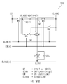
도 8은 본 발명의 제2 실시 예에 따른 발광 표시 장치의 구성을 개략적으로 보여주는 도면이다.FIG. 8 is a schematic view illustrating a configuration of a light emitting display according to a second embodiment of the present invention. Referring to FIG.
제2 실시 예에 따른 화소 회로를 구성하는 트랜지스터들은 모두 p 채널형이다. 이하 본 발명의 제1 실시 예와 다른 구성이 설명된다. The transistors constituting the pixel circuit according to the second embodiment are all p-channel type. Hereinafter, configurations other than the first embodiment of the present invention will be described.
도 8을 참조하면, 본 발명의 제1 실시 예와 비교하여, 본 발명의 제2 실시 예에 따른 발광 표시 장치(2)는 제3 스캔 드라이버(30) 대신 EL 전원 스캔 드라이버(60)를 포함한다. EL 전원 스캔 드라이버(60)는 각 화소 회로(100)의 캐소드 전원 전압을 제어하는 구동 회로이다. EL 전원 스캔 드라이버(60)는 행 단위로 화소 회로들(100)에 대응하여 구비된 EL 전원선(61~63)에 EL 전원 전압(ELVSS(n))을 공급한다.8, the light emitting
도 9는 본 발명의 제2 실시 예에 따른 단위 화소의 회로 구성을 보여주는 회로도이다.9 is a circuit diagram showing a circuit configuration of a unit pixel according to a second embodiment of the present invention.
도 9를 참조하면, 본 발명의 제1 실시 예와 비교하여 본 발명의 제2 실시 예에 따른 화소 회로(100)에서 트랜지스터들(M3,M4)이 게이트 제어 신호(EM(n))에 의해 동시에 제어된다. EL 전원선(65)은 발광 소자(3)의 캐소드 측의 단자에 접속된다. EL 전원선(65)은 EL 전원 스캔 드라이버(60)로부터 고전압 또는 저전압을 제공받는다.9, the transistors M3 and M4 in the
도 10a 내지 도 10d는 본 발명의 제2 실시 예에 따른 단위 화소의 동작 상태를 보여주는 회로도이다. 도 11은 본 발명의 제2 실시 예에 따른 단위 화소의 타이밍차트이다.10A to 10D are circuit diagrams showing an operation state of a unit pixel according to a second embodiment of the present invention. 11 is a timing chart of a unit pixel according to the second embodiment of the present invention.
도 10a 내지 도 10d를 참조하면, 단위 화소의 구동 방법은 (a) 초기화 기간, (b) VTH 보상 기간, (c) 데이터 프로그램 기간, 및 (d) 발광 기간을 포함한다. 도 10a 내지 도 10d에 도시된 (a) 초기화 기간, (b) VTH 보상 기간, (c) 데이터 프로그램 기간, 및 (d) 발광 기간은 도 11에 도시된 (a) 초기화 기간, (b) VTH 보상 기간, (c) 데이터 프로그램 기간, 및 (d) 발광 기간에 대응된다. 도 10에서 화살표는 전류의 방향을 나타낸다.10A to 10D, a method of driving a unit pixel includes (a) an initialization period, (b) a VTH compensation period, (c) a data programming period, and (d) a light emission period. (A) initialization period, (b) VTH compensation period, (c) data programming period, and (d) emission period shown in FIGS. 10A to 10D, A compensation period, (c) a data programming period, and (d) a light emission period. In Fig. 10, the arrow indicates the direction of the current.
(a) 초기화 기간 (a) Initialization period
데이터 신호(DT)로서 초기화 전압(VINIT)이 화소 회로(100)에 제공된다. 게이트 제어 신호(SCAN)가 로우 레벨로 되어, 트랜지스터들(M2,M5)이 온 된다. 게이트 제어 신호(EM)가 하이 레벨로 되어, 트랜지스터들(M3,M4)이 오프 된다. The initialization voltage VINIT is supplied to the
노드(N1)에는 트랜지스터(M2)를 통해 애노드 전압(ELVDD)이 제공되고, 노드(N3)에는 트랜지스터(M5)를 통해 초기화 전압(VINIT)이 제공된다. The node N1 is supplied with the anode voltage ELVDD through the transistor M2 and the node N3 is supplied with the initializing voltage VINIT through the transistor M5.
EL 전원 전압(ELVSS)은 하이 레벨(VRES)이므로, 발광 소자(3)의 기생 용량(CEL)에 의해 용량 결합된 발광 소자(3)의 애노드 측의 단자의 전위는 구동 트랜지스터(M1)가 온 될때까지 상승된다. 온 된 구동 트랜지스터(M1)를 통해 노드(N2)의 전위도 상승된다. 이러한 동작에 의해, 용량 소자(C1)에 초기화 전압(VINIT)과 하이 레벨 전압(VRES)에 의해 결정되는 전압(초기화 전압 및 하이 레벨 전압의 차이값)이 충전된다.The potential of the anode-side terminal of the light-emitting
본 발명의 제2 실시 예에서, 발광 소자(3)의 애노드측의 단자가 애노드 전압(ELVDD) + 문턱 전압(VTH) 보다 높아지도록 EL 전원 전압(ELVSS)이 변화된다. 본 발명의 제2 실시 예에 따른 구동 방법에 의해, 초기화 시점에서 문턱 전압(VTH) 보상이 수행될 수 있다. 이러한 동작은 후술될 것이다.In the second embodiment of the present invention, the EL power supply voltage ELVSS is changed such that the terminal on the anode side of the
(b) VTH 보상 기간 (b) VTH coverage period
데이터 신호(DT)로서 초기화 전압(VINIT)이 화소 회로(100)에 제공된다. 게이트 제어 신호(SCAN)는 로우 레벨이므로, 트랜지스터들(M2,M5)은 온 상태이다. 게이트 제어 신호(EM)는 하이 레벨로 유지되므로, 트랜지스터들(M3,M4)은 오프 상태를 유지한다. The initialization voltage VINIT is supplied to the
EL 전원 전압(ELVSS)은 로우 레벨이므로, 발광 소자(3)의 기생 용량(CEL)에 의해 용량 결합된 발광 소자(3)의 애노드 측의 단자의 전위도 낮아진다. 그 결과, 구동 트랜지스터(M1)의 소스 및드레인간의 전위차가 초기화 기간에 비해 반전된다. 따라서, 용량 소자(C1)에 축적된 전하가 구동 트랜지스터(M1)을 통해 발광 소자(3) 방향으로 이동된다. The potential of the anode-side terminal of the light-emitting
전하의 이동에 의해 노드(N2)의 전위는 낮아져, 애노드 전압(ELVDD) + 문턱 전압(VTH)으로 되고, 구동 트랜지스터(M1)가 오프되어, 안정된다. 즉, 용량 소자(C1)에 문턱값 전압으로 결정되는 전압이 충전된다.The potential of the node N2 is lowered by the movement of the charges to become the anode voltage ELVDD + the threshold voltage VTH, and the driving transistor M1 is turned off and stabilized. That is, the capacitor C1 is charged with a voltage determined as the threshold voltage.
구동 트랜지스터(M1)를 통해 이동된 전하의 일부는 발광 소자(3)의 다이오드 소자(D1)을 통해 흐르지만, 용량 소자(C1)의 용량을 고려하면, 발광 소자(3)의 다이오드 소자(D1)로 흐르는 전류는 매우 작으므로, 발광에는 기여하지 않는다. A part of the electric charge moved through the driving transistor M1 flows through the diode element D1 of the
이러한 문턱 전압(VTH) 보상은 도 11에 도시된 바와 같이, (a) 초기화 기간과 (d) 발광 기간 사이에 복수회 수행될 수 있다. 문턱 전압(VTH) 보상이 복수회 수행됨으로써, 보다 정밀하게 문턱 전압(VTH) 보상이 수행될 수 있다. This threshold voltage (VTH) compensation can be performed a plurality of times between (a) the initialization period and (d) the light emission period, as shown in FIG. By performing the threshold voltage (VTH) compensation a plurality of times, the threshold voltage (VTH) compensation can be performed more precisely.
(c) 데이터 프로그램 기간 (c) Data Program Period
전환 회로(50)에 의해 데이터 신호(DT)는 초기화 전압(VINIT)에서 계조 데이터 전압(VDATA)으로 전환된다. 게이트 제어 신호(SCAN)가 로우 레벨로 유지되고, 게이트 제어 신호(EM)가 하이 레벨로 유지되므로, 계조 데이터 전압(VDATA)이 노드(N3)에 제공된다. The switching
노드(N3)가 초기화 전압(VINIT)(저전압)으로부터 계조 데이터 전압(VDATA)(고전압)으로 전환된다. 따라서, 노드(N3)의 전위 상승에 따라서 용량 소자(C1)에 의해 용량 결합된 노드(N2)의 전위도 상승된다. 구동 트랜지스터(M1)의 게이트 전극에는 애노드 전압(ELVDD)이 공급되지만, 노드(N2)의 전압 상승에 따라서, 구동 트랜지스터(M1)의 소스 및 게이트 전위차(VGS)가 구동 트랜지스터(M1)의 고유의 문턱 전압(VTH)을 초과하면, 구동 트랜지스터(M1)가 온 된다.The node N3 is switched from the initialization voltage VINIT (low voltage) to the gradation data voltage VDATA (high voltage). Therefore, the potential of the node N2 capacitively coupled by the capacitive element C1 also rises in accordance with the potential rise of the node N3. The anode voltage ELVDD is supplied to the gate electrode of the driving transistor M1 but the source and gate potential difference VGS of the driving transistor Ml are different from each other depending on the voltage of the node N2, When the threshold voltage VTH is exceeded, the driving transistor Ml is turned on.
용량 소자(C1)에 축적된 전하는 구동 트랜지스터(M1)를 통해 발광 소자(3)로 흐르고, 노드(N2)의 전위가 애노드 전압(ELVDD) + 문턱 전압(VTH )으로 되면, 구동 트랜지스터(M1)가 오프되어 안정된다. 이 때, 용량 소자(C1)에는 애노드 전압(ELVDD) + 문턱 전압(VTH)과 계조 데이터 전압(VDATA)의 차이 값에 대응하는 전압이 충전된다. 즉, 용량 소자(C1)에 계조 데이터 전압과 문턱 전압으로 결정되는 전압이 충전된다.When the electric charge accumulated in the capacitor element C1 flows to the
이 때, 용량 소자(C1)에 축적된 전하가 구동 트랜지스터(M1)를 통해 발광 소자(3)로 흐르지만, 용량 소자(C1)의 용량을 고려하면, 발광 소자(3)의 다이오드 소자(D1)로 흐르는 전류은 매우 작으므로, 발광에는 기여하지 않는다.At this time, the charge accumulated in the capacitor element C1 flows to the
(d) 발광 기간 (d)
게이트 제어 신호(SCAN)는 하이 레벨로 되어, 트랜지스터들(M2, M5)이 오프된다. 게이트 제어 신호(EM)는 로우 레벨로 되어, 트랜지스터들(M3, M4)이 온 됨으로써, 노드(N2)에 애노드 전압(ELVDD)이 제공된다. The gate control signal SCAN becomes high level, and the transistors M2 and M5 are turned off. The gate control signal EM becomes a low level and the transistors M3 and M4 are turned on so that the anode voltage ELVDD is supplied to the node N2.
본 발명의 제1 실시 예의 동작과 유사하게, 애노드 전압(ELVDD)으로부터 공급된 전류 중, 용량 소자(C1)에 충전된 계조 데이터 전압과 문턱 전압으로 결정되는 전압에 대응하는 전류, 즉, 문턱 전압(VTH)이 보상된 계조 데이터 전압에 대응하는 전류가 구동 트랜지스터(M1)를 통해 발광 소자(3)에 공급됨으로써, 발광 소자(3)가 발광된다.Similarly to the operation of the first embodiment of the present invention, among the current supplied from the anode voltage ELVDD, the current corresponding to the voltage determined by the threshold voltage and the gradation data voltage charged in the capacitor C1, The current corresponding to the compensated gradation data voltage is supplied to the
도 12는 본 발명의 제2 실시 예에 따른 발광 표시 장치의 타이밍차트이다.12 is a timing chart of the light emitting display device according to the second embodiment of the present invention.
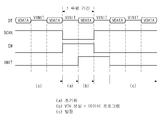
이하, 도 8 및 도 12를 참조하여, 복수의 화소 회로들(100)의 동작이 설명된다. 예시적으로, 도 12에 도시된 발광 표시 장치의 타이밍 차트을 사용하여, 도 8에서 화소 회로들(100) 중, 제1 열, 제1 행의 화소 회로(100C) 및 제1 열 제2 행의 화소 회로(100D)의 동작이 설명될 것이다.Hereinafter, with reference to Figs. 8 and 12, the operation of the plurality of
도 8 및 도 12를 참조하면, 도 12의 기간(1)에서, 데이터 신호(DT)로서 초기화 전압(VINIT)이 화소 회로(100C)에 제공된다. 게이트 제어 신호(SCAN(1))는 로우 레벨, 게이트 제어 신호(EM(1))는 하이 레벨, 및 EL 전원 전압(ELVSS(1))은 하이 레벨이므로, 화소 회로(100C)가 초기화 된다. 이 때, 화소 회로(100C)는 (a) 초기화 기간에 해당된다.Referring to Figs. 8 and 12, in the period (1) of Fig. 12, the initialization voltage VINIT is provided as the data signal DT to the
도 12의 기간(2)에서, 데이터 제어 신호(DT)로서 초기화 전압(VINIT)이 화소 회로(100C)에 제공된다. 게이트 제어 신호들(SCAN(1), SCAN(2)) 및 EL 전원 전압(ELVSS(1))은 로우 레벨로 되고, 게이트 제어 신호들(EM(1), EM(2)) 및 EL 전원 전압(ELVSS(2))은 하이 레벨로 됨으로써, 화소 회로(100C)에 대해 문턱 전압(VTH) 보상이 수행되고, 화소 회로(100D)는 초기화 된다. 이 때, 화소 회로(100C)는 (b) VTH 보상 기간에 해당되고, 화소 회로(100D)는 (a) 초기화 기간에 해당된다.In the period (2) of Fig. 12, the initialization voltage VINIT is provided to the
도 12의 기간(3)에서, 도시하지 않았지만, 제3 행의 화소 회로가 초기화되고, 화소 회로들(100C 및 100D)에서 문턱 전압(VTH) 보상이 수행된다. 이 때, 화소 회로들(100C 및 100D)은 함께 (b) VTH 보상 기간에 해당된다. 이후, 제4 행 이후의 화소 회로가 순차적으로 초기화되는 동안, 화소 회로들(100C 및 100D)에서 복수회의 문턱 전압(VTH) 보상이 수행되므로, 보다 정밀하게 문턱 전압(VTH) 보상이 수행될 수 있다. In the period (3) of Fig. 12, although not shown, the pixel circuit of the third row is initialized, and the threshold voltage (VTH) compensation is performed in the
도 12의 기간(4)에서, 데이터 제어 신호(DT)로서 계조 데이터 전압(VDATA)이 화소 회로(100C)에 제공된다. 게이트 제어 신호(SCAN(1))는 로우 레벨로 유지되므로, 용량 소자(C1)에 계조 데이터 전압과 문턱 전압으로 결정되는 전압이 충전된다. 이 때, 화소 회로(100C)는 (c) 데이터 프로그램 기간에 해당된다. In the period (4) of Fig. 12, the gradation data voltage VDATA is provided to the
도 12의 기간(5)에서, 게이트 제어 신호(SCAN(1))는 하이 레벨로 되고, 게이트 제어 신호(EM(1))는 로우 레벨로 됨으로써, 화소 회로(100C)의 구동 트랜지스터(M1)는 용량 소자(C1)에 충전된 전압에 대응하는 전류를 발광 소자(3)에 공급한다. 이 때, 화소 회로(100C)는 (d) 발광 기간에 해당된다. 또한, 이 때 화소 회로(100D)는 (b) VTH 보상 기간에 해당된다. The gate control signal SCAN (1) is at the high level and the gate control signal EM (1) is at the low level in the period (5) of FIG. 12, To the
이러한 동작들이 화소 회로들에서 반복되어, 본 발명의 실시 예에서, 순차적으로 초기화, VTH 보상, 및 데이터 프로그램을 포함하는 비발광 상태 및 발광 상태가 교대로 반복됨으로써, 도 6에 도시된 바와 같이 발광 표시 장치(2)가 프로그레시브 구동으로 동작될 수 있다.These operations are repeated in the pixel circuits. In the embodiment of the present invention, the non-emission state and the light emission state including sequential initialization, VTH compensation, and data program are alternately repeated, The
본 발명의 제2 실시 예에서, 화소 회로들에 대해 초기화 기간과 발광 기간 사이에서 문턱 전압(VTH) 보상이 복수회 수행된다. 따라서, 보다 정밀하게 문턱 전압(VTH) 보상이 수행될 수 있다.In the second embodiment of the present invention, the threshold voltage (VTH) compensation is performed a plurality of times between the initialization period and the light emission period for the pixel circuits. Therefore, the threshold voltage (VTH) compensation can be performed more precisely.
도 13은 본 발명의 제2 실시 예에 따른 제1 실시 예에 따른 문턱 전압 보상 시의 문턱 전압마다의 게이트 및 소스 전위차의 전압 변화를 나타낸 도면이다.FIG. 13 is a diagram showing a voltage change of a gate and a source potential difference for each threshold voltage at the time of threshold voltage compensation according to the first embodiment according to the second embodiment of the present invention.
도 13에는 서로 다른 문턱 전압(VTH1,VTH2)을 갖는 구동 트랜지스터들의 게이트 및 소스 전위차들(VGS)의 전압 변화가 도시되어 있다. 도 13에서 IDS는 구동 트랜지스터의 드레인 및 소스 간 전류이고, VGS는 구동 트랜지스터의 게이트 및 소스간 전압이다.13 shows the voltage variation of the gate and source potential differences VGS of the driving transistors having different threshold voltages VTH1 and VTH2. 13, IDS is the drain-source current of the driving transistor, and VGS is the gate-source voltage of the driving transistor.
도 13에서, 동작 스텝에 의해 소스와 드레인이 바뀌지만, 설명의 편를 위해, 게이트 및 소스 전위차(VGS)는 구동 트랜지스터(M1)의 게이트와 애노드 전원(ELVDD) 측의 단자(용량 소자(C1)과 트랜지스터(M4)에 접속되어 있는 단자) 사이의 전위차라 한다. 또한, 도 13에 있어서, 컷 오프 전압(Y1)을 갖는 구동 트랜지스터의 문턱 전압 특성을 문턱 전압(VTH1)이라 하고, 컷 오프 전압(Y2)을 갖는 구동 트랜지스터의 문턱 전압 특성을 문턱 전압(VTH2)라 칭한다.13, the source and drain are changed by the operation step. However, for ease of explanation, the gate and source potential difference VGS are set such that the gate of the driving transistor M1 and the terminal (the capacitor C1) on the anode power source ELVDD side And a terminal connected to the transistor M4). 13, the threshold voltage characteristic of the driving transistor having the cut-off voltage Y1 is referred to as a threshold voltage VTH1 and the threshold voltage characteristic of the driving transistor having the cut-off voltage Y2 is referred to as a threshold voltage VTH2. Quot;
도 13을 참조하면, 2 개의 구동 트랜지스터들(M1)에는 EL 전원 전압(ELVSS)측으로부터 동일한 전압이 공급된다. 그러나, 구동 트랜지스터들을 통해 EL 전원 전압(ELVSS)이 화소 회로들에 공급되기 때문에, 구동 트랜지스터의 문턱 전압(VTH1)으로 인해, 초기화 전압(VINIT1)이 화소 회로에 공급되고 구동 트랜지스터의 문턱 전압(VTH2)으로 인해 초기화 전압(VINIT2)이 화소 회로에 공급된다. Referring to Fig. 13, the two driving transistors M1 are supplied with the same voltage from the EL power supply voltage ELVSS side. However, since the EL power supply voltage ELVSS is supplied to the pixel circuits through the driving transistors, the initializing voltage VINIT1 is supplied to the pixel circuit due to the threshold voltage VTH1 of the driving transistor, and the threshold voltage VTH2 The initializing voltage VINIT2 is supplied to the pixel circuit.
X1 상태와 X2 상태에서 전류량이 근접하므로, 문턱 전압(VTH) 보상이 이루어지는 것이 확인된다. 그 다음, 초기화 전압(VINIT)의 공급이 정지되면, 각각의 문턱 전압(VTH1,VTH2)의 특성에 따라서 VGS에 대응하는 IDS가 흐른다. 따라서, 2 개의 구동 트랜지스터들(M1)의 VGS들이 저하하여, 각각의 컷 오프 전압(Y1,Y2)에 도달하면, 2 개의 구동 트랜지스터들(M1)이 오프된다. 구동 트랜지스터들(M1)은 동일한 IDS로 컷 오프된다. It is confirmed that the threshold voltage (VTH) compensation is performed because the amount of current is close in the X1 state and the X2 state. Then, when the supply of the initializing voltage VINIT is stopped, the IDS corresponding to the VGS flows according to the characteristics of the threshold voltages VTH1 and VTH2. Therefore, when the VGSs of the two driving transistors M1 are lowered to reach the respective cut-off voltages Y1 and Y2, the two driving transistors M1 are turned off. The driving transistors M1 are cut off to the same IDS.
본 발명의 제2 실시 예에서, 실시예 1의 화소 회로에서 얻을 수 있는 효과에 더하여, 초기화 동작에서의 보상 및 복수회의 문턱 전압(VTH) 보상이 수행되기 때문에 보다 정밀하게 문턱 전압(VTH) 보상이 수행될 수 있다. In the second embodiment of the present invention, the compensation in the initializing operation and the compensation of the threshold voltage (VTH) are performed in addition to the effect obtained in the pixel circuit of the first embodiment, so that the threshold voltage (VTH) compensation Can be performed.
(실시 형태 3)(Embodiment 3)
도 14는 본 발명의 제3 실시 예에 따른 단위 화소의 회로 구성을 보여주는 회로도이다.14 is a circuit diagram showing a circuit configuration of a unit pixel according to the third embodiment of the present invention.
제3 실시 예에 따른 화소 회로를 구성하는 트랜지스터들은 모두 n 채널형이다. 이하 본 발명의 제1 실시 예와 다른 구성이 설명된다. 도 14를 참조하면,발광 소자(3)의 애노드 측의 단자는 애노드 전원(ELVDD)에 접속된다. 구동 트랜지스터(M1)의 제1 단자는 발광 소자 (3)의 캐소드 측의 단자에 접속된다. 구동 트랜지스터(M1)는 구동 트랜지스터(M1)의 게이트 전극으로 공급되는 전압에 따라서 발광 소자(3)로 공급되는 전류의 크기를 제어한다.All the transistors constituting the pixel circuit according to the third embodiment are n-channel type. Hereinafter, configurations other than the first embodiment of the present invention will be described. 14, the terminal on the anode side of the
구동 트랜지스터(M1)의 게이트와 캐소드 전원선(96) 사이에 게이트 제어 신호(SCAN(n))로 제어되는 트랜지스터(M2)가 접속된다. 구동 트랜지스터(M1)의 게이트 전극에는, 게이트 제어 신호(EM(n))로 제어되는 트랜지스터(M3)의 제1 단자가 접속된다. 트랜지스터(M3)의 제2 단자는 용량 소자(C1)을 통해 구동 트랜지스터(M1)의 제2 단자에 접속된다. A transistor M2 controlled by a gate control signal SCAN (n) is connected between the gate of the driving transistor Ml and the cathode
구동 트랜지스터(M1)의 제2 단자와 캐소드 전원선(96) 사이에 게이트 제어 신호(INIT(n))에 의해 제어되는 트랜지스터(M4)가 접속된다. 트랜지스터(M3)의 제2 단자와 데이터 선(46) 사이에 게이트 제어 신호(SCAN(n))로 제어되는 트랜지스터(M5)가 접속된다.The transistor M4 controlled by the gate control signal INIT (n) is connected between the second terminal of the driving transistor Ml and the cathode
도 15는 본 발명의 제3 실시 예에 따른 발광 표시 장치의 타이밍차트이다.15 is a timing chart of the light emitting display device according to the third embodiment of the present invention.
도 14와 같이 화소 회로(100)의 모든 트랜지스터들(M1~M5)이 n 채널형으로 바뀜으로써, 제어 신호들(SCAN, EM, INIT)의 하이 레벨 및 로우 레벨이 제1 실시 예와 달리 반전된다. 14, all the transistors M1 to M5 of the
즉, 도 15에 도시된 타이밍차트는 도 4의 제어 신호들의 하이 레벨 및 로우 레벨이 반전된 것이고, 화소 회로(100)의 트랜지스터들(M1~M5)의 구동은 실시예 1과 동일하므로, 트랜지스터들(M1~M5)의 구동에 대한 구체적인 설명은 생략된다. That is, the timing chart shown in Fig. 15 is obtained by inverting the high level and the low level of the control signals of Fig. 4, and the driving of the transistors M1 to M5 of the
본 발명의 제3 실시 예에 따른 화소 회로는 실시예 1의 화소 회로 구성을 기본으로 하여 n 채널형 트랜지스터들을 포함하고 있으나, 이에 한정되지 않고, 실시 예 2의 회로 구성을 기본으로 하여 n 채널형 트랜지스터들을 포함할 수도 있다. The pixel circuit according to the third embodiment of the present invention includes the n-channel transistors based on the pixel circuit configuration of the first embodiment, but the present invention is not limited thereto, and the n- Transistors.
이상과 같이 화소 회로(100)의 트랜지스터들(M1~M5)이 모두 n 채널 형인 경우에도, 본 발명이 적용될 수 있다. n 채널형 트랜지스터의 이동도는 p 채널형 트랜지스터의 이동도보다 높기 때문에, 실시예 1의 효과에 더하여 보다 고속 동작이 수행될 수 있다.As described above, the present invention can also be applied to the case where all the transistors M1 to M5 of the
또한, n 채널형 트랜지스터들로 화소 회로가 구성될 수 있으므로,, 아몰퍼스 실리콘 트랜지스터나 산화물 반도체 트랜지스터로 구성된 발광 표시 장치에도 본 발명의 화소 회로가 적용될 수 있다.Further, since the pixel circuit can be constituted by n-channel transistors, the pixel circuit of the present invention can be applied to a light emitting display device composed of an amorphous silicon transistor or an oxide semiconductor transistor.
(실시 형태 4)(Fourth Embodiment)
도 16은 본 발명의 제4 실시 예에 따른 발광 표시 장치의 구성을 개략적으로 보여주는 도면이다. 도 17은 본 발명의 제4 실시 예에 따른 발광 표시 장치의 수평 기간 타이밍차트이다. 도 18은 본 발명의 제4 실시 예에 따른 발광 표시 장치의 수직 기간 타이밍차트이다. 도 19는 본 발명의 제4 실시 예에 따른 발광 표시 장치의 구동 방법을 보여주는 도면이다.FIG. 16 is a view schematically showing a configuration of a light emitting display according to a fourth embodiment of the present invention. 17 is a horizontal period timing chart of the light emitting display according to the fourth embodiment of the present invention. 18 is a vertical period timing chart of the light emitting display according to the fourth embodiment of the present invention. 19 is a view illustrating a driving method of a light emitting display according to a fourth embodiment of the present invention.
도 8의 표시 장치(2)를 기본 구성으로 하여 도 8의 표시 장치(2)에서 입력 신호를 변경함으로서 도 16의 발광 표시 장치가 구현될 수 있다. 구체적으로, 도 16의 발광 표시 장치(2)는 제2 스캔 드라이버(20)와 EL 전원 스캔 드라이버(60)를 제외하고 도 8의 표시 장치(2)와 동일한 구성을 갖고, 입력 신호를 변경함으로써 사이멀테니어스 구동을 수행할 수 있다. 예를 들어, 도 16에 도시된 발광 표시 장치(2)는, 게이트 제어 신호들(EM(n), ELVSS(n))이 행 단위가 아니라 공통으로 화소 회로들(100)에 제공되는 구성을 제외하고, 도 8에 도시된 제2 실시 예의 발광 표시 장치(2)와 동일한 구성을 갖는다. The light emitting display device of Fig. 16 can be implemented by changing the input signal in the
실시예 2와 달리, 초기화, VTH 보상, 데이터 프로그램, 및 발광 동작이 모든 화소 회로들(100)에서 동시에 수행됨으로써, 도 19에 도시된 바와 같이 발광 표시 장치(2)는 사이멀테니어스 구동 방식으로 구동될 수 있다. 19, initialization, VTH compensation, data programming, and light emission operation are simultaneously performed in all the
여기서, 도 17 및 도 18에 도시된 바와 같이, 게이트 제어 신호들(EM(n)과 ELVSS(n))이 행 단위로 제어되지 않고, 모든 화소 회로들(100)에 동시에 제공되도록 제어될 수 있다. Here, as shown in Figs. 17 and 18, the gate control signals EM (n) and ELVSS (n) can be controlled to be simultaneously supplied to all the
즉, 도 16에 도시된 바와 같이, 게이트 제어 신호들(EM(n), ELVSS(n))이 동시에 화소들에 제공되므로써, 도 8에 도시된 제2 스캔 드라이버(20)와 EL 전원 스캔 드라이버(60)가 도 16에 도시된 발광 표시 장치(2)에서 사용되지 않을 수 있다. 8, the
또한, 도 8 및 도 16에 도시된 셔터 안경(70)은 후술되는 3차원(3D) 영상의 표시 시에 표시 장치(2)와 동기되도록 제어된다.The
전술한 바와 같이 모든 화소 회로들(100)이 동시에 구동되기 위해, 제어 신호들이 공통으로 화소 회로들에 제공된다. 이러한 구성으로 인해 제 2 스캔 드라이버(20)와 EL 전원 스캔 드라이버(60)가 제거될 수 있어, 표시 장치의 표시 패널에 내장되는 스캔 드라이버 회로의 크기가 줄어들 수 있다. 일반적으로 스캔 드라이버는 표시 패널 영역의 비표시 영역에 배치되므로, 스캔 드라이버의 크기를 줄임으로써 내로우 베젤 (narrow frame)이 구현될 수 있다.As described above, in order for all the
제4 실시 예에서 제2 실시 예의 발광 표시 장치를 이용하여 제어 신호를 공통화하고, 사이멀테니어스 구동이 수행되었으나, 이에 한정되지 않고, 실시 예 1이나 실시 예 3의 발광 표시 장치를 이용하여 제4 실시 예의 발광 표시 장치가 구현될 수도 있다.In the fourth embodiment, the control signal is made common using the light emitting display device of the second embodiment, and the driving of the semiconductor is performed. However, the present invention is not limited to this, and the light emitting display device of
(실시 형태 5)(Embodiment 5)
도 20은 본 발명의 제5 실시 예에 따른 표시 모드의 상태를 보여주는 도면이다. 도 21은 본 발명의 제5 실시 예에 따른 발광 표시 장치의 구동 방법을 보여주는 도면이다.20 is a view showing a state of a display mode according to a fifth embodiment of the present invention. 21 is a diagram illustrating a method of driving a light emitting display according to a fifth embodiment of the present invention.
도 20 및 도 21에서는 도 8에 도시된 제2 실시 예의 표시 장치(2)에서 입력 신호를 변경함으로써, 프로그레시브 구동 및 사이멀테니어스 구동의 변환 예가 도시된다. 20 and 21 show an example of conversion of the progressive drive and the medialtening drive by changing the input signal in the
도 20을 참조하면, 표시 모드 1에서 발광 표시 장치는 프로그레시브 구동으로 구동된다. 따라서, 순차적으로 행 단위의 화소 회로들에서 초기화, VTH 보상 및 데이터 프로그램을 포함하는 비발광 동작 및 발광 동작이 교대로 수행된다. Referring to Fig. 20, in the
표시 모드 2에서 발광 표시 장치는 사이멀테니어스 구동으로 구동된다. 따라서, 모든 화소 회로들에서 초기화, VTH 보상 및 데이터 프로그램을 포함하는 비발광 동작 및 발광 동작이 수행된다.In the
사이멀테니어스 구동보다 프로그레시브 구동에서 발광 소자의 발광 듀티가 크다 발광 듀티를 크게 할 수 있는 프로그레시브 구동은, 발광 소자에 흐르는 피크 전류 값을 저감할 수 있기 때문에, 발광 소자에 흐르는 피크 전류에 의존하는 발광 소자의 수명(휘도 열화)이 늘어날 수 있다.The emission duty of the light emitting element in the progressive drive is larger than that in the magneto-optical drive. The progressive drive capable of increasing the light emission duty can reduce the peak current value flowing in the light emitting element. Therefore, The lifetime (luminance deterioration) of the light emitting element can be increased.
그러나, 프로그레시브 구동은 3차원(3D) 영상 표시 시에 일반적으로 사용되는 셔터 안경 방식에 사용될 수 없다. 셔터 안경 방식에 의한 3D 영상 표시는, 좌안(L)용 영상과 우안(R)용 영상이 교대로 표시됨과 동시에, 셔터 안경의 투과율이 0%와 100%로 전환됨으로써, 입체적인 영상이 표시되는 방식이다. However, the progressive drive can not be used in the shutter glasses system generally used in three-dimensional (3D) image display. In the 3D image display by the shutter glasses system, the images for the left eye (L) and the images for the right eye (R) are alternately displayed and the transmittance of the shutter glasses is switched to 0% and 100% to be.
프로그레시브 구동과 같이 1 수직 기간에서 표시가 완결되지 않은 구동 방법, 즉, 1 수직 기간의 이전 수직 기간 영상과 그 다음 수직 기간 영상이 혼재하는 구동 방법에서는, 3D 영상 표시가 실현될 수 없다.In a driving method in which display is not completed in one vertical period such as progressive driving, that is, in a driving method in which a previous vertical period image in one vertical period and a subsequent vertical period image are mixed, 3D image display can not be realized.
도 21을 참조하면, 화소 회로들은 프로그레시브 구동 및사이멀테니어스 구동이, 입력 신호을 바꿈으로서 함계 실현될 수 있다. Referring to Fig. 21, the pixel circuits can be realized by progressively driving and cyclotronous driving by changing the input signal.
구체적으로는 표시 장치(2)에 접속된 제어부(80)에 프로그레시브 구동을 선택하는 신호가 입력되면, 각 드라이버 회로가 도 11 및 도 12에 도시된 동작을 실행하도록 제어부(80)는 각 드라이버 회로를 제어한다. Specifically, when a signal for selecting the progressive drive is input to the
제어부(80)에 사이멀테니어스 구동을 선택하는 신호가 입력되면, 각 드라이버 회로가 도 17 및 도 18에 도시된 동작을 실행하도록 제어부(80)는 각 드라이버 회로를 제어한다. When a signal for selecting the remote control drive is input to the
또한, 사이멀테니어스 구동 시에 있어서는, 제어부(80)에서 셔터 안경(70)을 동시에 제어함으로써, 입체적인 영상을 제공한다. 구체적으로는 도 21에 나타내는 바와 같이, 사이멀테니어스 구동 시, 최초의 1 수직 기간에서 우안용 영상 데이터가 표시된다. 우안용 영상 데이터의 표시에 동기하여 셔터 안경(70)의 우안은 투과 상태, 좌안은 비투과 상태로 설정됨으로써, 셔터 안경(70)의 우안을 통해 우안용 영상 데이터가 시인된다. Further, at the time of driving the remote tenness, the
그 다음의 1 수직 기간에서 좌안용 영상 데이터가 표시된다. 좌안용 영상 데이터의 표시에 동기하여 셔터 안경(70)의 좌안은 투과 상태, 우안은 비투과 상태로 설정됨으로써, 셔터 안경(70)의 좌안을 통해 좌안용 영상 데이터가 시인된다. And the left eye image data is displayed in the next one vertical period. The left eye image data is visually confirmed through the left eye of the
이와 같이, 셔터 안경(70)의 우안을 통해 우안용 영상 데이터가 사용자에게 제공되고, 셔터 안경(70)의 좌안을 통해 좌안용 영상 데이터가 사용자에게 제공됨으로써, 입체적인 영상이 사용자에게 제공될 수 있다.Thus, the right eye image data is provided to the user through the right eye of the
이와 같이 하여, 화소 회로들에 제공되는 신호를 변경함으로써 프로그레시브 구동과 사이멀테니어스 구동이 전환될 수 있고, 표시 모드에 맞춰서 최적의 구동 방법이 선택되어 발광 표시 장치가 구동될 수 있다.In this way, by changing the signal provided to the pixel circuits, the progressive driving and the medialtening driving can be switched, and the optimum driving method can be selected in accordance with the display mode, and the light emitting display can be driven.
본 발명의 제1 내지 제3 실시 예에 있어서, 각각의 화소 회로(100)는 5개의 트랜지스터들(M1~M5) 및 1개의 용량 소자(C1)를 포함하고 있으나, 본 발명의 취지로부터 벗어나지 않는 범위에서 다양한 형태를 취할 수 있다. In each of the first to third embodiments of the present invention, each
구체적으로, 본 발명에 부가적인 기능을 추가하기 위한 목적으로 트랜지스터 수, 용량 소자 수나 신호선 수가 많아질 수 있다. 예를 들어, 계조 데이터 전압(VDATA)과 초기화 전압(VINIT)이 동일한 신호선을 통해 화소 회로에 제공되고 있으나, 이에 한정되지 않고 각각 별도의 신호선을 통해 화소 회로에 제공될 수 있다. Specifically, the number of transistors, the number of capacitor elements, and the number of signal lines can be increased for the purpose of adding an additional function to the present invention. For example, although the gradation data voltage VDATA and the initialization voltage VINIT are provided to the pixel circuit through the same signal line, the gradation data voltage VDATA and the initialization voltage VINIT may be provided to the pixel circuit through separate signal lines, respectively.
또한, 본 발명의 제1 내지 제4 실시 예에 있어서, (a)~(c)의 각 기간의 전환이 동시에 수행되고 있으나, 본 발명의 목적이 달성할 수 있는 범위 내에서 각 신호의 타이밍이 미뤄질 수 있다.In the first to fourth embodiments of the present invention, the switching of each of the periods (a) to (c) is performed at the same time, but the timing of each signal is within the range that the object of the present invention can achieve Can be delayed.
예를 들어, 초기화 기간에서, 트랜지스터(M3)가 온 된 상태에서 데이터 신호(DT)로서 초기화 전압(VINIT)이 화소 회로(100)에 제공되고, 트랜지스터들(M2, M5)이 온 되면, 애노드 전압(ELVDD)에서 초기화 전압(VINIT)으로 전류가 흘러버려 소비 전력이 증대될 수 있다. 따라서, 바람직하게, 트랜지스터(M3)가 오프된 이후에 트랜지스터들(M2, M5)이 온 될 수 있다. For example, in the initialization period, when the initialization voltage VINIT is supplied to the
또한, 발광 기간에 있어서, 트랜지스터들(M2, M5)을 오프하기 전에 트랜지스터(M3)가 온되면, 용량 소자(C1)에 충전된 계조 데이터 전압과 문턱값 전압으로 결정되는 전압이 갱신되어 버린다. 따라서, 바람직하게 트랜지스터들(M2,M5)이 오프된 이후에 트랜지스터(M3)가 온 될 수 있다.When the transistor M3 is turned on before the transistors M2 and M5 are turned off in the light emission period, the gradation data voltage charged in the capacitor C1 and the voltage determined as the threshold voltage are updated. Therefore, the transistor M3 can be turned on after the transistors M2 and M5 are preferably turned off.
이상 실시 예를 참조하여 설명하였지만, 해당 기술 분야의 숙련된 당업자는 하기의 특허 청구의 범위에 기재된 본 발명의 사상 및 영역으로부터 벗어나지 않는 범위 내에서 본 발명을 다양하게 수정 및 변경시킬 수 있음을 이해할 수 있을 것이다. 또한 본 발명에 개시된 실시 예는 본 발명의 기술 사상을 한정하기 위한 것이 아니고, 하기의 특허 청구의 범위 및 그와 동등한 범위 내에 있는 모든 기술 사상은 본 발명의 권리범위에 포함되는 것으로 해석되어야 할 것이다.It will be understood by those skilled in the art that various changes in form and details may be made therein without departing from the spirit and scope of the invention as defined in the appended claims. It will be possible. In addition, the embodiments disclosed in the present invention are not intended to limit the technical spirit of the present invention, and all technical ideas which fall within the scope of the following claims and equivalents thereof should be interpreted as being included in the scope of the present invention .
이상 실시 예를 참조하여 설명하였지만, 해당 기술 분야의 숙련된 당업자는 하기의 특허 청구의 범위에 기재된 본 발명의 사상 및 영역으로부터 벗어나지 않는 범위 내에서 본 발명을 다양하게 수정 및 변경시킬 수 있음을 이해할 수 있을 것이다. 또한 본 발명에 개시된 실시 예는 본 발명의 기술 사상을 한정하기 위한 것이 아니고, 하기의 특허 청구의 범위 및 그와 동등한 범위 내에 있는 모든 기술 사상은 본 발명의 권리범위에 포함되는 것으로 해석되어야 할 것이다.It will be understood by those skilled in the art that various changes in form and details may be made therein without departing from the spirit and scope of the invention as defined in the appended claims. It will be possible. In addition, the embodiments disclosed in the present invention are not intended to limit the technical spirit of the present invention, and all technical ideas which fall within the scope of the following claims and equivalents thereof should be interpreted as being included in the scope of the present invention .
1: 전자 기기 2: 표시 장치
3: 발광 소자 10: 제 1 스캔 드라이버
20: 제 2 스캔 드라이버 30: 제 3 스캔 드라이버
40: 데이터 드라이버 50: 전환 회로
60: EL 스캔 드라이버 80: 제어부
90: 전원
100,100A,100B,100C,100D,100E,100F: 화소 회로
11,12,13,14,15,16: 게이트 제어 신호선
21,22,23,24,25,26: 게이트 제어 신호선
31,32,33,34,36: 게이트 제어 신호선
41,42,43,44,45,46: 데이터 선
94,95: 애노드 전원선 96: 캐소드 전원선1: Electronic device 2: Display device
3: light emitting element 10: first scan driver
20: second scan driver 30: third scan driver
40: data driver 50: switching circuit
60: EL scan driver 80:
90: Power supply
100, 100A, 100B, 100C, 100D, 100E, 100F:
11, 12, 13, 14, 15, 16: gate control signal lines
21, 22, 23, 24, 25, 26: gate control signal line
31, 32, 33, 34, 36: gate control signal line
41, 42, 43, 44, 45, 46:
94, 95: anode power line 96: cathode power line
Claims (15)
게이트 전극에 공급되는 전압에 따라서 상기 발광 소자로 공급되는 상기 전류의 크기를 제어하고, 제1 단자가 상기 발광 소자의 한쪽의 단자에 접속된 제1 트랜지스터;
상기 제1 트랜지스터의 상기 게이트 전극과 제1 전원 사이에 접속된 제2 트랜지스터;
제1 단자가 상기 제1 트랜지스터의 상기 게이트 전극에 접속되고, 제2 단자가 용량 소자를 통해 상기 제1 트랜지스터의 제2 단자에 접속된 제3 트랜지스터;
상기 제1 트랜지스터의 상기 제2 단자와 제2 전원 사이에 접속된 제 4 트랜지스터; 및
상기 제3 트랜지스터의 제2 단자와 초기화 전압 및 계조 데이터 전압이 공급되는 신호선 사이에 접속된 제5 트랜지스터를 각각 갖는 화소 회로들이 매트릭스 형상으로 배치된 발광 표시 장치의 구동 방법에 있어서,
상기 용량 소자에 상기 초기화 전압을 충전하는 단계;
상기 용량 소자에 상기 계조 데이터 전압과 상기 제1 트랜지스터의 문턱 전압으로 결정되는 제1 데이터 전압을 충전하는 단계; 및
상기 용량 소자에 충전된 상기 제1 데이터 전압에 대응하는 전류가 상기 발광 소자에 공급되어 상기 발광 소자가 발광하는 단계를 포함하는 것을 특징으로 하는 표시 장치의 구동 방법.A light emitting element whose gradation is determined by the supplied current;
A first transistor for controlling the magnitude of the current supplied to the light emitting element according to a voltage supplied to the gate electrode, and having a first terminal connected to one terminal of the light emitting element;
A second transistor connected between the gate electrode of the first transistor and the first power supply;
A third transistor having a first terminal connected to the gate electrode of the first transistor and a second terminal connected to a second terminal of the first transistor through a capacitive element;
A fourth transistor connected between the second terminal of the first transistor and the second power supply; And
And a fifth transistor connected between a second terminal of the third transistor and a signal line to which the initialization voltage and the gradation data voltage are supplied, the method comprising:
Charging the capacitive element with the initialization voltage;
Charging the capacitive element with the first data voltage determined by the gradation data voltage and the threshold voltage of the first transistor; And
And a current corresponding to the first data voltage charged in the capacitive element is supplied to the light emitting element so that the light emitting element emits light.
상기 제1 데이터 전압을 충전하는 단계 전에 상기 용량 소자에 상기 문턱 전압으로 결정되는 전압을 충전하는 단계를 더 포함하는 것을 특징으로 하는 표시 장치의 구동 방법.The method according to claim 1,
Further comprising the step of charging the capacitor with a voltage determined as the threshold voltage before charging the first data voltage.
상기 초기화 전압을 충전하는 단계와 상기 발광 소자가 발광하는 단계 사이에서 상기 문턱 전압으로 결정되는 전압을 충전하는 단계가 복수회 수행되는 것을 특징으로 하는 표시 장치의 구동 방법.3. The method of claim 2,
Wherein the step of charging the voltage determined as the threshold voltage between the step of charging the initialization voltage and the step of emitting the light emitting element is performed a plurality of times.
상기 초기화 전압을 충전하는 단계에서,
상기 제3 트랜지스터를 오프 시키고, 상기 제3 트랜지스터를 오프 시킨 이후에, 상기 제2 트랜지스터를 온 시키고, 상기 제1 트랜지스터의 상기 게이트 전극에 상기 제1 트랜지스터를 오프 시키는 상기 제1 전원의 전압을 공급하고,
상기 제4 트랜지스터 및 상기 제 5 트랜지스터를 온 시켜 상기 용량 소자의 양 단자에 상기 제2 전원의 전압 및 상기 신호선의 상기 초기화 전압을 공급하는 것을 특징으로 하는 표시 장치의 구동 방법.The method according to claim 1,
In the step of charging the initialization voltage,
The first transistor is turned off, the third transistor is turned off, the second transistor is turned on, and the first transistor is turned off by the gate electrode of the first transistor, and,
And the fourth transistor and the fifth transistor are turned on to supply the voltage of the second power source and the initialization voltage of the signal line to both terminals of the capacitive element.
상기 발광 소자의 다른 쪽의 단자는 제3 전원에 접속되고,
상기 초기화 전압을 충전하는 단계에서,
상기 제3 트랜지스터를 오프시키고,
상기 제3 트랜지스터를 오프시킨 이후에, 상기 제5 트랜지스터를 온 시키고, 상기 용량 소자의 한쪽의 단자에 상기 제3 전원의 전압을 공급하고, 상기 제2 트랜지스터를 온 시키고, 상기 제1 트랜지스터의 게이트 전극에 상기 제1 전원의 전압을 공급하고,
상기 제3 전원의 전압을 변화시키고, 상기 발광 소자의 용량 성분의 용량 결합에 의해 상기 제1 트랜지스터가 온 되고, 상기 용량 소자에 상기 초기화 전압을 충전하는 것을 특징으로 하는 표시 장치의 구동 방법.3. The method according to claim 1 or 2,
The other terminal of the light emitting element is connected to the third power supply,
In the step of charging the initialization voltage,
The third transistor is turned off,
The third transistor is turned off, the fifth transistor is turned on, the voltage of the third power source is supplied to one terminal of the capacitor, the second transistor is turned on, and the gate of the first transistor Supplying a voltage of the first power source to the electrode,
Wherein the voltage of the third power source is changed and the first transistor is turned on by capacitance coupling of the capacitance component of the light emitting element to charge the capacitor element with the initialization voltage.
상기 문턱 전압으로 결정되는 전압을 충전하는 단계에서, 상기 초기화 전압을 충전하는 단계 후에, 상기 제1 트랜지스터가 오프되도록 상기 제1 전원 전압을 변화시키고, 상기 용량 소자에 상기 문턱 전압으로 결정되는 전압을 충전하는 것을 특징으로 하는 표시 장치의 구동 방법.3. The method of claim 2,
Wherein the step of charging the voltage determined by the threshold voltage changes the first power supply voltage so that the first transistor is turned off after charging the initialization voltage and a voltage determined as the threshold voltage And then charging the display device.
상기 발광 소자가 발광하는 단계에서,
상기 제2 트랜지스터 및 상기 제5 트랜지스터를 오프 시킨 이후에 상기 제3 트랜지스터를 온 시키고, 상기 제3 트랜지스터를 온 시킨 이후에 상기 제4 트랜지스터를 온 시키는 것을 특징으로 하는 표시 장치의 구동 방법.The method according to claim 1,
In the step of emitting the light emitting element,
The third transistor is turned on after the second transistor and the fifth transistor are turned off, and the fourth transistor is turned on after the third transistor is turned on.
상기 화소 회로들은 행 단위로 및 순차적으로 상기 초기화 전압을 충전하는 단계와 상기 제1 데이터 전압을 충전하는 단계를 포함하는 비발광 동작 및 상기 발광 소자가 발광하는 단계를 포함하는 발광 동작이 수행되는 프로그레시브 방식으로 상기 화소 회로들이 구동되는 것을 특징으로 하는 표시 장치의 구동 방법.The method according to claim 1,
Wherein the pixel circuits are arranged in a row-by-row and sequential manner, the step of charging the initialization voltage, and the step of charging the first data voltage, and the step of emitting light by the light emitting element, And the pixel circuits are driven in a method of driving the display device.
상기 모든 화소들에서 상기 초기화 전압을 충전하는 단계와 상기 제1 데이터 전압을 충전하는 단계를 포함하는 비발광 동작 및 상기 발광 소자가 발광하는 단계를 포함하는 발광 동작이 수행되는 사이멀테니어스 방식으로 상기 화소 회로들이 구동 되는 것을 특징으로 하는 표시 장치의 구동 방법.The method according to claim 1,
A non-light emitting operation including a step of charging the initialization voltage in all of the pixels and a step of charging the first data voltage, and a step of emitting light by the light emitting element, And the pixel circuits are driven.
상기 초기화 전압을 충전하는 단계와 상기 제1 데이터 전압을 충전하는 단계를 포함하는 비발광 동작 및 상기 발광 소자가 발광하는 단계를 포함하는 발광 동작이 행 단위로 순차적으로 수행되는 프로그레시브 구동과,
상기 초기화 전압을 충전하는 단계와 상기 제1 데이터 전압을 충전하는 단계를 포함하는 비발광 동작 및 상기 발광 소자가 발광하는 단계를 포함하는 발광 동작이 모든 화소 회로들에서 수행되는 사이멀테니어스 구동이 입력된 전환 신호에 의해 전환되는 것을 특징으로 하는 표시 장치의 구동 방법.The method according to claim 1,
A non-light emitting operation including a step of charging the initialization voltage and a step of charging the first data voltage, and a step of emitting light by the light emitting element are sequentially performed in a row unit,
Emitting operation including a step of charging the initialization voltage and a step of charging the first data voltage and a step of emitting light by the light emitting element are performed in all the pixel circuits, Wherein the switching signal is switched by an input switching signal.
게이트 전극에 공급되는 전압에 따라서 상기 발광 소자로 공급되는 상기 전류의 크기를 제어하고, 제1 단자가 상기 발광 소자의 한쪽의 단자에 접속된 제1 트랜지스터;
상기 제1 트랜지스터의 상기 게이트 전극과 제1 전원 사이에 접속된 제2 트랜지스터;
제1 단자가 상기 제1 트랜지스터의 상기 게이트 전극에 접속되고, 제2 단자가 용량 소자를 통해 상기 제1 트랜지스터의 제2 단자에 접속된 제3 트랜지스터;
상기 제1 트랜지스터의 상기 제2 단자와 제2 전원 사이에 접속된 제4 트랜지스터; 및
상기 제3 트랜지스터의 제2 단자와 초기화 전압 및 계조 데이터 전압이 공급되는 신호선 사이에 접속된 제5 트랜지스터를 포함하는 발광 표시 장치.A light emitting element including a parasitic capacitance and having a gradation determined by a supplied current;
A first transistor for controlling the magnitude of the current supplied to the light emitting element according to a voltage supplied to the gate electrode, and having a first terminal connected to one terminal of the light emitting element;
A second transistor connected between the gate electrode of the first transistor and the first power supply;
A third transistor having a first terminal connected to the gate electrode of the first transistor and a second terminal connected to a second terminal of the first transistor through a capacitive element;
A fourth transistor connected between the second terminal of the first transistor and the second power supply; And
And a fifth transistor connected between a second terminal of the third transistor and a signal line to which an initialization voltage and a gradation data voltage are supplied.
상기 제1 전원의 전압과 상기 제2 전원의 전압은 동일한 전원선을 통해 공급되는 것을 특징으로 하는 발광 표시 장치.13. The method of claim 12,
Wherein the voltage of the first power source and the voltage of the second power source are supplied through the same power source line.
상기 제3 트랜지스터의 게이트 전극과 상기 제4 트랜지스터의 게이트 전극은 동일한 제어선에 접속되는 것을 특징으로 하는 발광 표시 장치.13. The method of claim 12,
And the gate electrode of the third transistor and the gate electrode of the fourth transistor are connected to the same control line.
상기 제2 트랜지스터의 게이트 전극과 상기 제5 트랜지스터의 게이트 전극은 동일한 제어선에 접속되는 것을 특징으로 하는 발광 표시 장치.
13. The method of claim 12,
And the gate electrode of the second transistor and the gate electrode of the fifth transistor are connected to the same control line.
Applications Claiming Priority (2)
| Application Number | Priority Date | Filing Date | Title |
|---|---|---|---|
| JP2013138160A JP2015011274A (en) | 2013-07-01 | 2013-07-01 | Light-emitting display device and method for driving the same |
| JPJP-P-2013-138160 | 2013-07-01 |
Publications (2)
| Publication Number | Publication Date |
|---|---|
| KR20150003667A true KR20150003667A (en) | 2015-01-09 |
| KR102198874B1 KR102198874B1 (en) | 2021-01-06 |
Family
ID=52115167
Family Applications (1)
| Application Number | Title | Priority Date | Filing Date |
|---|---|---|---|
| KR1020140073762A Active KR102198874B1 (en) | 2013-07-01 | 2014-06-17 | Light emitting display apparatus and driving method thereof |
Country Status (3)
| Country | Link |
|---|---|
| US (2) | US9437136B2 (en) |
| JP (1) | JP2015011274A (en) |
| KR (1) | KR102198874B1 (en) |
Cited By (4)
| Publication number | Priority date | Publication date | Assignee | Title |
|---|---|---|---|---|
| KR20170114211A (en) * | 2016-03-29 | 2017-10-13 | 엘지디스플레이 주식회사 | Organic Light Emitting Display Device |
| KR20180066327A (en) * | 2016-12-07 | 2018-06-19 | 삼성디스플레이 주식회사 | Display device and driving method thereof |
| KR20180066330A (en) * | 2016-12-07 | 2018-06-19 | 삼성디스플레이 주식회사 | Display device and driving method thereof |
| US10417959B2 (en) | 2016-06-20 | 2019-09-17 | Samsung Display Co., Ltd. | Display panel, a display device, and a method of driving a display panel |
Families Citing this family (15)
| Publication number | Priority date | Publication date | Assignee | Title |
|---|---|---|---|---|
| TWI546786B (en) * | 2014-08-22 | 2016-08-21 | 友達光電股份有限公司 | Display panel |
| KR20160148790A (en) * | 2015-06-16 | 2016-12-27 | 삼성디스플레이 주식회사 | Organic light emitting disply device and method for driving an organic light emitting display device |
| JP6721328B2 (en) * | 2015-12-21 | 2020-07-15 | 株式会社ジャパンディスプレイ | Display device |
| CN107293259B (en) * | 2016-03-29 | 2019-07-12 | 乐金显示有限公司 | Organic Light Emitting Diode Display |
| CN106448555B (en) | 2016-12-16 | 2019-11-12 | 上海天马有机发光显示技术有限公司 | Organic light emitting display panel, driving method thereof and organic light emitting display device |
| CN106531085B (en) | 2017-01-05 | 2019-05-24 | 上海天马有机发光显示技术有限公司 | Organic light emitting display panel and its driving method, organic light-emitting display device |
| KR102740962B1 (en) | 2017-01-10 | 2024-12-12 | 삼성디스플레이 주식회사 | Display device and driving method thereof |
| US10796642B2 (en) * | 2017-01-11 | 2020-10-06 | Samsung Display Co., Ltd. | Display device |
| KR102369284B1 (en) * | 2017-06-01 | 2022-03-04 | 삼성디스플레이 주식회사 | Organic Light Emitting Display Device and Driving Method Thereof |
| CN107818768B (en) * | 2017-10-10 | 2019-09-17 | 惠科股份有限公司 | Driving method and driving device of display device |
| WO2020065961A1 (en) * | 2018-09-28 | 2020-04-02 | シャープ株式会社 | Display device |
| TWI758600B (en) * | 2019-04-09 | 2022-03-21 | 友達光電股份有限公司 | Display panel and display panel driving method |
| CN110558778A (en) * | 2019-09-04 | 2019-12-13 | 山东省立医院 | Neonate carries strutting arrangement with arms |
| CN110599955B (en) * | 2019-09-19 | 2021-02-09 | 昆山工研院新型平板显示技术中心有限公司 | Display panel and display device |
| KR102873024B1 (en) * | 2021-04-23 | 2025-10-17 | 삼성전자주식회사 | Electronic device including display and method of operation therof |
Citations (3)
| Publication number | Priority date | Publication date | Assignee | Title |
|---|---|---|---|---|
| KR20070027265A (en) * | 2005-09-06 | 2007-03-09 | 엘지.필립스 엘시디 주식회사 | LED display device |
| KR20080091926A (en) * | 2007-04-10 | 2008-10-15 | 삼성에스디아이 주식회사 | Pixel and organic light emitting display device using same and driving method thereof |
| KR20130062573A (en) * | 2011-12-05 | 2013-06-13 | 엘지디스플레이 주식회사 | Organic light emitting diode display device and method of driving the same |
Family Cites Families (18)
| Publication number | Priority date | Publication date | Assignee | Title |
|---|---|---|---|---|
| KR101103868B1 (en) * | 2004-07-29 | 2012-01-12 | 엘지디스플레이 주식회사 | Driving circuit of organic light emitting display |
| JP2006309104A (en) * | 2004-07-30 | 2006-11-09 | Sanyo Electric Co Ltd | Active-matrix-driven display device |
| JP4752315B2 (en) * | 2005-04-19 | 2011-08-17 | セイコーエプソン株式会社 | Electronic circuit, driving method thereof, electro-optical device, and electronic apparatus |
| KR101139529B1 (en) * | 2005-06-30 | 2012-05-02 | 엘지디스플레이 주식회사 | Oled |
| JP3982544B2 (en) | 2005-07-26 | 2007-09-26 | セイコーエプソン株式会社 | Electronic circuit, electro-optical device, and electronic apparatus |
| KR100624137B1 (en) * | 2005-08-22 | 2006-09-13 | 삼성에스디아이 주식회사 | Pixel circuit of organic electroluminescent display and driving method thereof |
| KR100732828B1 (en) * | 2005-11-09 | 2007-06-27 | 삼성에스디아이 주식회사 | Pixel and light emitting display device using same |
| JP2008241832A (en) | 2007-03-26 | 2008-10-09 | Seiko Epson Corp | Liquid crystal device, pixel circuit, active matrix substrate, and electronic device |
| KR100931469B1 (en) * | 2008-02-28 | 2009-12-11 | 삼성모바일디스플레이주식회사 | Pixel and organic light emitting display device using same |
| KR101509113B1 (en) * | 2008-12-05 | 2015-04-08 | 삼성디스플레이 주식회사 | Display device and driving method thereof |
| JP5287210B2 (en) | 2008-12-17 | 2013-09-11 | ソニー株式会社 | Display device and electronic device |
| JP2010250111A (en) | 2009-04-16 | 2010-11-04 | Hitachi Ltd | Display device for time division binocular stereoscopic vision |
| KR20110013693A (en) | 2009-08-03 | 2011-02-10 | 삼성모바일디스플레이주식회사 | Organic electroluminescent display and driving method thereof |
| KR101100947B1 (en) * | 2009-10-09 | 2011-12-29 | 삼성모바일디스플레이주식회사 | Organic light emitting display device and driving method thereof |
| KR101125571B1 (en) * | 2010-02-05 | 2012-03-22 | 삼성모바일디스플레이주식회사 | Pixel, display device and driving method thereof |
| KR101142644B1 (en) * | 2010-03-17 | 2012-05-03 | 삼성모바일디스플레이주식회사 | Organic Light Emitting Display Device |
| KR20120065716A (en) * | 2010-12-13 | 2012-06-21 | 삼성모바일디스플레이주식회사 | Display device and driving method thereof |
| CN103226931B (en) * | 2013-04-27 | 2015-09-09 | 京东方科技集团股份有限公司 | Image element circuit and organic light emitting display |
-
2013
- 2013-07-01 JP JP2013138160A patent/JP2015011274A/en active Pending
-
2014
- 2014-06-17 KR KR1020140073762A patent/KR102198874B1/en active Active
- 2014-07-01 US US14/321,002 patent/US9437136B2/en active Active
-
2016
- 2016-09-02 US US15/255,528 patent/US10068527B2/en active Active
Patent Citations (3)
| Publication number | Priority date | Publication date | Assignee | Title |
|---|---|---|---|---|
| KR20070027265A (en) * | 2005-09-06 | 2007-03-09 | 엘지.필립스 엘시디 주식회사 | LED display device |
| KR20080091926A (en) * | 2007-04-10 | 2008-10-15 | 삼성에스디아이 주식회사 | Pixel and organic light emitting display device using same and driving method thereof |
| KR20130062573A (en) * | 2011-12-05 | 2013-06-13 | 엘지디스플레이 주식회사 | Organic light emitting diode display device and method of driving the same |
Cited By (4)
| Publication number | Priority date | Publication date | Assignee | Title |
|---|---|---|---|---|
| KR20170114211A (en) * | 2016-03-29 | 2017-10-13 | 엘지디스플레이 주식회사 | Organic Light Emitting Display Device |
| US10417959B2 (en) | 2016-06-20 | 2019-09-17 | Samsung Display Co., Ltd. | Display panel, a display device, and a method of driving a display panel |
| KR20180066327A (en) * | 2016-12-07 | 2018-06-19 | 삼성디스플레이 주식회사 | Display device and driving method thereof |
| KR20180066330A (en) * | 2016-12-07 | 2018-06-19 | 삼성디스플레이 주식회사 | Display device and driving method thereof |
Also Published As
| Publication number | Publication date |
|---|---|
| US20150002558A1 (en) | 2015-01-01 |
| JP2015011274A (en) | 2015-01-19 |
| US20170004774A1 (en) | 2017-01-05 |
| US9437136B2 (en) | 2016-09-06 |
| KR102198874B1 (en) | 2021-01-06 |
| US10068527B2 (en) | 2018-09-04 |
Similar Documents
| Publication | Publication Date | Title |
|---|---|---|
| KR102198874B1 (en) | Light emitting display apparatus and driving method thereof | |
| US9693045B2 (en) | Organic light emitting display and driving method thereof | |
| KR101788432B1 (en) | Pixel circuit, organic electroluminescent display panel, display apparatus and driving method thereof | |
| CN104409047B (en) | Pixel driving circuit, pixel driving method and display device | |
| US7612749B2 (en) | Driving circuits for displays | |
| JP4144462B2 (en) | Electro-optical device and electronic apparatus | |
| US9852687B2 (en) | Display device and driving method | |
| CN101615376B (en) | Display device | |
| US8325112B2 (en) | Organic light emitting display and method of driving thereof | |
| US9262966B2 (en) | Pixel circuit, display panel and display apparatus | |
| US8582715B2 (en) | Stage circuit and scan driver using the same | |
| TWI417843B (en) | Dual pixel unit and dual driver circuit | |
| TWI427597B (en) | Display and driving method thereof | |
| KR20140132275A (en) | Pixel circuit and driving method thereof | |
| JP2011112724A (en) | Display device, method of driving the same and electronic equipment | |
| KR20160141366A (en) | Organic Light Emitting Display and Circuit thereof | |
| KR20190067344A (en) | Light emitting display apparatus and method for driving thereof | |
| JP2009037123A (en) | Active matrix display device and driving method thereof | |
| CN107369412B (en) | Pixel circuit, driving method thereof and display device | |
| KR102215242B1 (en) | Display apparatus and driving method of display apparatus | |
| CN104700782A (en) | OELD pixel circuit, display device and control method | |
| CN102956201B (en) | Pixel circuit, driving method and display device of pixel circuit | |
| WO2020019158A1 (en) | Pixel driving circuit, method, and display apparatus | |
| KR20170124061A (en) | Organic Light Emitting Display and Circuit thereof | |
| US10068523B2 (en) | Display device |
Legal Events
| Date | Code | Title | Description |
|---|---|---|---|
| PA0109 | Patent application |
Patent event code: PA01091R01D Comment text: Patent Application Patent event date: 20140617 |
|
| PG1501 | Laying open of application | ||
| A201 | Request for examination | ||
| PA0201 | Request for examination |
Patent event code: PA02012R01D Patent event date: 20190603 Comment text: Request for Examination of Application Patent event code: PA02011R01I Patent event date: 20140617 Comment text: Patent Application |
|
| E902 | Notification of reason for refusal | ||
| PE0902 | Notice of grounds for rejection |
Comment text: Notification of reason for refusal Patent event date: 20200715 Patent event code: PE09021S01D |
|
| E701 | Decision to grant or registration of patent right | ||
| PE0701 | Decision of registration |
Patent event code: PE07011S01D Comment text: Decision to Grant Registration Patent event date: 20201019 |
|
| GRNT | Written decision to grant | ||
| PR0701 | Registration of establishment |
Comment text: Registration of Establishment Patent event date: 20201229 Patent event code: PR07011E01D |
|
| PR1002 | Payment of registration fee |
Payment date: 20201230 End annual number: 3 Start annual number: 1 |
|
| PG1601 | Publication of registration | ||
| PR1001 | Payment of annual fee |
Payment date: 20241125 Start annual number: 5 End annual number: 5 |