KR20140040675A - Multi-level memory arrays with memory cells that employ bipolar storage elements and methods of forming the same - Google Patents
Multi-level memory arrays with memory cells that employ bipolar storage elements and methods of forming the same Download PDFInfo
- Publication number
- KR20140040675A KR20140040675A KR20137012138A KR20137012138A KR20140040675A KR 20140040675 A KR20140040675 A KR 20140040675A KR 20137012138 A KR20137012138 A KR 20137012138A KR 20137012138 A KR20137012138 A KR 20137012138A KR 20140040675 A KR20140040675 A KR 20140040675A
- Authority
- KR
- South Korea
- Prior art keywords
- metal
- reservoir
- bipolar
- memory cell
- layer
- Prior art date
- Legal status (The legal status is an assumption and is not a legal conclusion. Google has not performed a legal analysis and makes no representation as to the accuracy of the status listed.)
- Withdrawn
Links
- 230000015654 memory Effects 0.000 title claims abstract description 340
- 238000000034 method Methods 0.000 title claims description 48
- 238000003491 array Methods 0.000 title description 8
- 238000003860 storage Methods 0.000 title description 4
- 239000000463 material Substances 0.000 claims description 166
- 239000002184 metal Substances 0.000 claims description 131
- 229910052751 metal Inorganic materials 0.000 claims description 130
- 239000010936 titanium Substances 0.000 claims description 85
- 229910044991 metal oxide Inorganic materials 0.000 claims description 71
- 150000004706 metal oxides Chemical class 0.000 claims description 71
- 229910052710 silicon Inorganic materials 0.000 claims description 58
- 239000010703 silicon Substances 0.000 claims description 58
- 239000004065 semiconductor Substances 0.000 claims description 33
- 238000006243 chemical reaction Methods 0.000 claims description 32
- 150000004767 nitrides Chemical class 0.000 claims description 32
- -1 tungsten nitride Chemical class 0.000 claims description 26
- 229910052721 tungsten Inorganic materials 0.000 claims description 20
- 239000010937 tungsten Substances 0.000 claims description 20
- 230000002441 reversible effect Effects 0.000 claims description 16
- NRTOMJZYCJJWKI-UHFFFAOYSA-N Titanium nitride Chemical compound [Ti]#N NRTOMJZYCJJWKI-UHFFFAOYSA-N 0.000 claims description 14
- MZLGASXMSKOWSE-UHFFFAOYSA-N tantalum nitride Chemical compound [Ta]#N MZLGASXMSKOWSE-UHFFFAOYSA-N 0.000 claims description 11
- OGIDPMRJRNCKJF-UHFFFAOYSA-N titanium oxide Inorganic materials [Ti]=O OGIDPMRJRNCKJF-UHFFFAOYSA-N 0.000 description 57
- XUIMIQQOPSSXEZ-UHFFFAOYSA-N Silicon Chemical compound [Si] XUIMIQQOPSSXEZ-UHFFFAOYSA-N 0.000 description 56
- ATJFFYVFTNAWJD-UHFFFAOYSA-N Tin Chemical compound [Sn] ATJFFYVFTNAWJD-UHFFFAOYSA-N 0.000 description 49
- 229910021332 silicide Inorganic materials 0.000 description 35
- 239000001301 oxygen Substances 0.000 description 33
- 229910052760 oxygen Inorganic materials 0.000 description 33
- FVBUAEGBCNSCDD-UHFFFAOYSA-N silicide(4-) Chemical compound [Si-4] FVBUAEGBCNSCDD-UHFFFAOYSA-N 0.000 description 32
- 239000004020 conductor Substances 0.000 description 29
- 229910008484 TiSi Inorganic materials 0.000 description 24
- 230000004888 barrier function Effects 0.000 description 20
- 238000000137 annealing Methods 0.000 description 18
- QVGXLLKOCUKJST-UHFFFAOYSA-N atomic oxygen Chemical compound [O] QVGXLLKOCUKJST-UHFFFAOYSA-N 0.000 description 18
- 230000015572 biosynthetic process Effects 0.000 description 17
- 238000000151 deposition Methods 0.000 description 17
- 230000008569 process Effects 0.000 description 16
- RTAQQCXQSZGOHL-UHFFFAOYSA-N Titanium Chemical compound [Ti] RTAQQCXQSZGOHL-UHFFFAOYSA-N 0.000 description 15
- 229910052719 titanium Inorganic materials 0.000 description 15
- 239000013078 crystal Substances 0.000 description 11
- 230000008021 deposition Effects 0.000 description 11
- 230000007704 transition Effects 0.000 description 10
- OKTJSMMVPCPJKN-UHFFFAOYSA-N Carbon Chemical compound [C] OKTJSMMVPCPJKN-UHFFFAOYSA-N 0.000 description 9
- 238000010586 diagram Methods 0.000 description 9
- WFKWXMTUELFFGS-UHFFFAOYSA-N tungsten Chemical compound [W] WFKWXMTUELFFGS-UHFFFAOYSA-N 0.000 description 9
- 229910000577 Silicon-germanium Inorganic materials 0.000 description 8
- LEVVHYCKPQWKOP-UHFFFAOYSA-N [Si].[Ge] Chemical compound [Si].[Ge] LEVVHYCKPQWKOP-UHFFFAOYSA-N 0.000 description 8
- 150000002739 metals Chemical class 0.000 description 8
- 229910021420 polycrystalline silicon Inorganic materials 0.000 description 8
- 239000000758 substrate Substances 0.000 description 8
- 229910017052 cobalt Inorganic materials 0.000 description 7
- 239000010941 cobalt Substances 0.000 description 7
- GUTLYIVDDKVIGB-UHFFFAOYSA-N cobalt atom Chemical compound [Co] GUTLYIVDDKVIGB-UHFFFAOYSA-N 0.000 description 7
- 239000010408 film Substances 0.000 description 7
- 229910052732 germanium Inorganic materials 0.000 description 7
- GNPVGFCGXDBREM-UHFFFAOYSA-N germanium atom Chemical compound [Ge] GNPVGFCGXDBREM-UHFFFAOYSA-N 0.000 description 7
- 229920005591 polysilicon Polymers 0.000 description 7
- VYPSYNLAJGMNEJ-UHFFFAOYSA-N Silicium dioxide Chemical compound O=[Si]=O VYPSYNLAJGMNEJ-UHFFFAOYSA-N 0.000 description 6
- 239000003989 dielectric material Substances 0.000 description 6
- 229910052715 tantalum Inorganic materials 0.000 description 5
- GUVRBAGPIYLISA-UHFFFAOYSA-N tantalum atom Chemical compound [Ta] GUVRBAGPIYLISA-UHFFFAOYSA-N 0.000 description 5
- 229910021341 titanium silicide Inorganic materials 0.000 description 5
- IJGRMHOSHXDMSA-UHFFFAOYSA-N Atomic nitrogen Chemical compound N#N IJGRMHOSHXDMSA-UHFFFAOYSA-N 0.000 description 4
- GWEVSGVZZGPLCZ-UHFFFAOYSA-N Titan oxide Chemical compound O=[Ti]=O GWEVSGVZZGPLCZ-UHFFFAOYSA-N 0.000 description 4
- 230000008901 benefit Effects 0.000 description 4
- 229910052799 carbon Inorganic materials 0.000 description 4
- 229910000449 hafnium oxide Inorganic materials 0.000 description 4
- WIHZLLGSGQNAGK-UHFFFAOYSA-N hafnium(4+);oxygen(2-) Chemical compound [O-2].[O-2].[Hf+4] WIHZLLGSGQNAGK-UHFFFAOYSA-N 0.000 description 4
- 238000004519 manufacturing process Methods 0.000 description 4
- 229920002120 photoresistant polymer Polymers 0.000 description 4
- LIVNPJMFVYWSIS-UHFFFAOYSA-N silicon monoxide Chemical compound [Si-]#[O+] LIVNPJMFVYWSIS-UHFFFAOYSA-N 0.000 description 4
- 230000005641 tunneling Effects 0.000 description 4
- 229910052581 Si3N4 Inorganic materials 0.000 description 3
- 229910045601 alloy Inorganic materials 0.000 description 3
- 239000000956 alloy Substances 0.000 description 3
- 238000000231 atomic layer deposition Methods 0.000 description 3
- 238000002425 crystallisation Methods 0.000 description 3
- 230000008025 crystallization Effects 0.000 description 3
- 239000007772 electrode material Substances 0.000 description 3
- 238000005530 etching Methods 0.000 description 3
- 229910052757 nitrogen Inorganic materials 0.000 description 3
- HQVNEWCFYHHQES-UHFFFAOYSA-N silicon nitride Chemical compound N12[Si]34N5[Si]62N3[Si]51N64 HQVNEWCFYHHQES-UHFFFAOYSA-N 0.000 description 3
- ZOKXTWBITQBERF-UHFFFAOYSA-N Molybdenum Chemical compound [Mo] ZOKXTWBITQBERF-UHFFFAOYSA-N 0.000 description 2
- 229910003087 TiOx Inorganic materials 0.000 description 2
- 238000009792 diffusion process Methods 0.000 description 2
- SCCCLDWUZODEKG-UHFFFAOYSA-N germanide Chemical compound [GeH3-] SCCCLDWUZODEKG-UHFFFAOYSA-N 0.000 description 2
- 229910021389 graphene Inorganic materials 0.000 description 2
- 229910002804 graphite Inorganic materials 0.000 description 2
- 239000010439 graphite Substances 0.000 description 2
- 238000011065 in-situ storage Methods 0.000 description 2
- 229910052750 molybdenum Inorganic materials 0.000 description 2
- 239000011733 molybdenum Substances 0.000 description 2
- QGLKJKCYBOYXKC-UHFFFAOYSA-N nonaoxidotritungsten Chemical compound O=[W]1(=O)O[W](=O)(=O)O[W](=O)(=O)O1 QGLKJKCYBOYXKC-UHFFFAOYSA-N 0.000 description 2
- 230000001590 oxidative effect Effects 0.000 description 2
- BPUBBGLMJRNUCC-UHFFFAOYSA-N oxygen(2-);tantalum(5+) Chemical compound [O-2].[O-2].[O-2].[O-2].[O-2].[Ta+5].[Ta+5] BPUBBGLMJRNUCC-UHFFFAOYSA-N 0.000 description 2
- 235000012239 silicon dioxide Nutrition 0.000 description 2
- 239000000377 silicon dioxide Substances 0.000 description 2
- 229910052814 silicon oxide Inorganic materials 0.000 description 2
- 229910001936 tantalum oxide Inorganic materials 0.000 description 2
- 238000012360 testing method Methods 0.000 description 2
- HLLICFJUWSZHRJ-UHFFFAOYSA-N tioxidazole Chemical compound CCCOC1=CC=C2N=C(NC(=O)OC)SC2=C1 HLLICFJUWSZHRJ-UHFFFAOYSA-N 0.000 description 2
- 229910001930 tungsten oxide Inorganic materials 0.000 description 2
- 235000012431 wafers Nutrition 0.000 description 2
- 229910052727 yttrium Inorganic materials 0.000 description 2
- 229910052580 B4C Inorganic materials 0.000 description 1
- BQCADISMDOOEFD-UHFFFAOYSA-N Silver Chemical compound [Ag] BQCADISMDOOEFD-UHFFFAOYSA-N 0.000 description 1
- 238000003917 TEM image Methods 0.000 description 1
- 229910008486 TiSix Inorganic materials 0.000 description 1
- 229910003481 amorphous carbon Inorganic materials 0.000 description 1
- 229910021417 amorphous silicon Inorganic materials 0.000 description 1
- 239000006117 anti-reflective coating Substances 0.000 description 1
- 238000004380 ashing Methods 0.000 description 1
- INAHAJYZKVIDIZ-UHFFFAOYSA-N boron carbide Chemical compound B12B3B4C32B41 INAHAJYZKVIDIZ-UHFFFAOYSA-N 0.000 description 1
- 229910021393 carbon nanotube Inorganic materials 0.000 description 1
- 239000002041 carbon nanotube Substances 0.000 description 1
- 239000003575 carbonaceous material Substances 0.000 description 1
- 150000004770 chalcogenides Chemical class 0.000 description 1
- 150000001875 compounds Chemical class 0.000 description 1
- 238000013461 design Methods 0.000 description 1
- 230000005684 electric field Effects 0.000 description 1
- 238000011066 ex-situ storage Methods 0.000 description 1
- 230000001747 exhibiting effect Effects 0.000 description 1
- 230000006870 function Effects 0.000 description 1
- 239000007789 gas Substances 0.000 description 1
- 238000005247 gettering Methods 0.000 description 1
- 238000002513 implantation Methods 0.000 description 1
- 238000005468 ion implantation Methods 0.000 description 1
- 230000000873 masking effect Effects 0.000 description 1
- 238000002156 mixing Methods 0.000 description 1
- 238000012986 modification Methods 0.000 description 1
- 230000004048 modification Effects 0.000 description 1
- 239000002243 precursor Substances 0.000 description 1
- 238000012545 processing Methods 0.000 description 1
- 238000004151 rapid thermal annealing Methods 0.000 description 1
- 230000009467 reduction Effects 0.000 description 1
- 238000000926 separation method Methods 0.000 description 1
- HBMJWWWQQXIZIP-UHFFFAOYSA-N silicon carbide Chemical compound [Si+]#[C-] HBMJWWWQQXIZIP-UHFFFAOYSA-N 0.000 description 1
- 229910010271 silicon carbide Inorganic materials 0.000 description 1
- 230000007480 spreading Effects 0.000 description 1
- 238000003892 spreading Methods 0.000 description 1
- 239000010409 thin film Substances 0.000 description 1
Images


Classifications
-
- H—ELECTRICITY
- H10—SEMICONDUCTOR DEVICES; ELECTRIC SOLID-STATE DEVICES NOT OTHERWISE PROVIDED FOR
- H10N—ELECTRIC SOLID-STATE DEVICES NOT OTHERWISE PROVIDED FOR
- H10N70/00—Solid-state devices having no potential barriers, and specially adapted for rectifying, amplifying, oscillating or switching
- H10N70/20—Multistable switching devices, e.g. memristors
-
- G—PHYSICS
- G11—INFORMATION STORAGE
- G11C—STATIC STORES
- G11C11/00—Digital stores characterised by the use of particular electric or magnetic storage elements; Storage elements therefor
- G11C11/56—Digital stores characterised by the use of particular electric or magnetic storage elements; Storage elements therefor using storage elements with more than two stable states represented by steps, e.g. of voltage, current, phase, frequency
- G11C11/5685—Digital stores characterised by the use of particular electric or magnetic storage elements; Storage elements therefor using storage elements with more than two stable states represented by steps, e.g. of voltage, current, phase, frequency using storage elements comprising metal oxide memory material, e.g. perovskites
-
- G—PHYSICS
- G11—INFORMATION STORAGE
- G11C—STATIC STORES
- G11C13/00—Digital stores characterised by the use of storage elements not covered by groups G11C11/00, G11C23/00, or G11C25/00
- G11C13/0002—Digital stores characterised by the use of storage elements not covered by groups G11C11/00, G11C23/00, or G11C25/00 using resistive RAM [RRAM] elements
- G11C13/0007—Digital stores characterised by the use of storage elements not covered by groups G11C11/00, G11C23/00, or G11C25/00 using resistive RAM [RRAM] elements comprising metal oxide memory material, e.g. perovskites
-
- G—PHYSICS
- G11—INFORMATION STORAGE
- G11C—STATIC STORES
- G11C13/00—Digital stores characterised by the use of storage elements not covered by groups G11C11/00, G11C23/00, or G11C25/00
- G11C13/0002—Digital stores characterised by the use of storage elements not covered by groups G11C11/00, G11C23/00, or G11C25/00 using resistive RAM [RRAM] elements
- G11C13/0021—Auxiliary circuits
- G11C13/0069—Writing or programming circuits or methods
-
- H—ELECTRICITY
- H10—SEMICONDUCTOR DEVICES; ELECTRIC SOLID-STATE DEVICES NOT OTHERWISE PROVIDED FOR
- H10B—ELECTRONIC MEMORY DEVICES
- H10B63/00—Resistance change memory devices, e.g. resistive RAM [ReRAM] devices
- H10B63/20—Resistance change memory devices, e.g. resistive RAM [ReRAM] devices comprising selection components having two electrodes, e.g. diodes
-
- H—ELECTRICITY
- H10—SEMICONDUCTOR DEVICES; ELECTRIC SOLID-STATE DEVICES NOT OTHERWISE PROVIDED FOR
- H10B—ELECTRONIC MEMORY DEVICES
- H10B63/00—Resistance change memory devices, e.g. resistive RAM [ReRAM] devices
- H10B63/80—Arrangements comprising multiple bistable or multi-stable switching components of the same type on a plane parallel to the substrate, e.g. cross-point arrays
- H10B63/84—Arrangements comprising multiple bistable or multi-stable switching components of the same type on a plane parallel to the substrate, e.g. cross-point arrays arranged in a direction perpendicular to the substrate, e.g. 3D cell arrays
-
- H—ELECTRICITY
- H10—SEMICONDUCTOR DEVICES; ELECTRIC SOLID-STATE DEVICES NOT OTHERWISE PROVIDED FOR
- H10N—ELECTRIC SOLID-STATE DEVICES NOT OTHERWISE PROVIDED FOR
- H10N70/00—Solid-state devices having no potential barriers, and specially adapted for rectifying, amplifying, oscillating or switching
- H10N70/011—Manufacture or treatment of multistable switching devices
- H10N70/021—Formation of switching materials, e.g. deposition of layers
-
- H—ELECTRICITY
- H10—SEMICONDUCTOR DEVICES; ELECTRIC SOLID-STATE DEVICES NOT OTHERWISE PROVIDED FOR
- H10N—ELECTRIC SOLID-STATE DEVICES NOT OTHERWISE PROVIDED FOR
- H10N70/00—Solid-state devices having no potential barriers, and specially adapted for rectifying, amplifying, oscillating or switching
- H10N70/20—Multistable switching devices, e.g. memristors
- H10N70/24—Multistable switching devices, e.g. memristors based on migration or redistribution of ionic species, e.g. anions, vacancies
-
- H—ELECTRICITY
- H10—SEMICONDUCTOR DEVICES; ELECTRIC SOLID-STATE DEVICES NOT OTHERWISE PROVIDED FOR
- H10N—ELECTRIC SOLID-STATE DEVICES NOT OTHERWISE PROVIDED FOR
- H10N70/00—Solid-state devices having no potential barriers, and specially adapted for rectifying, amplifying, oscillating or switching
- H10N70/801—Constructional details of multistable switching devices
- H10N70/821—Device geometry
- H10N70/826—Device geometry adapted for essentially vertical current flow, e.g. sandwich or pillar type devices
-
- H—ELECTRICITY
- H10—SEMICONDUCTOR DEVICES; ELECTRIC SOLID-STATE DEVICES NOT OTHERWISE PROVIDED FOR
- H10N—ELECTRIC SOLID-STATE DEVICES NOT OTHERWISE PROVIDED FOR
- H10N70/00—Solid-state devices having no potential barriers, and specially adapted for rectifying, amplifying, oscillating or switching
- H10N70/801—Constructional details of multistable switching devices
- H10N70/841—Electrodes
-
- H—ELECTRICITY
- H10—SEMICONDUCTOR DEVICES; ELECTRIC SOLID-STATE DEVICES NOT OTHERWISE PROVIDED FOR
- H10N—ELECTRIC SOLID-STATE DEVICES NOT OTHERWISE PROVIDED FOR
- H10N70/00—Solid-state devices having no potential barriers, and specially adapted for rectifying, amplifying, oscillating or switching
- H10N70/801—Constructional details of multistable switching devices
- H10N70/881—Switching materials
- H10N70/883—Oxides or nitrides
- H10N70/8833—Binary metal oxides, e.g. TaOx
-
- G—PHYSICS
- G11—INFORMATION STORAGE
- G11C—STATIC STORES
- G11C13/00—Digital stores characterised by the use of storage elements not covered by groups G11C11/00, G11C23/00, or G11C25/00
- G11C13/0002—Digital stores characterised by the use of storage elements not covered by groups G11C11/00, G11C23/00, or G11C25/00 using resistive RAM [RRAM] elements
- G11C13/0021—Auxiliary circuits
- G11C13/0069—Writing or programming circuits or methods
- G11C2013/0073—Write using bi-directional cell biasing
-
- G—PHYSICS
- G11—INFORMATION STORAGE
- G11C—STATIC STORES
- G11C2213/00—Indexing scheme relating to G11C13/00 for features not covered by this group
- G11C2213/50—Resistive cell structure aspects
- G11C2213/55—Structure including two electrodes, a memory active layer and at least two other layers which can be a passive or source or reservoir layer or a less doped memory active layer
-
- G—PHYSICS
- G11—INFORMATION STORAGE
- G11C—STATIC STORES
- G11C2213/00—Indexing scheme relating to G11C13/00 for features not covered by this group
- G11C2213/50—Resistive cell structure aspects
- G11C2213/56—Structure including two electrodes, a memory active layer and a so called passive or source or reservoir layer which is NOT an electrode, wherein the passive or source or reservoir layer is a source of ions which migrate afterwards in the memory active layer to be only trapped there, to form conductive filaments there or to react with the material of the memory active layer in redox way
-
- G—PHYSICS
- G11—INFORMATION STORAGE
- G11C—STATIC STORES
- G11C2213/00—Indexing scheme relating to G11C13/00 for features not covered by this group
- G11C2213/70—Resistive array aspects
- G11C2213/71—Three dimensional array
-
- G—PHYSICS
- G11—INFORMATION STORAGE
- G11C—STATIC STORES
- G11C2213/00—Indexing scheme relating to G11C13/00 for features not covered by this group
- G11C2213/70—Resistive array aspects
- G11C2213/72—Array wherein the access device being a diode
Landscapes
- Engineering & Computer Science (AREA)
- Chemical & Material Sciences (AREA)
- Materials Engineering (AREA)
- Computer Hardware Design (AREA)
- Manufacturing & Machinery (AREA)
- Semiconductor Memories (AREA)
Abstract
제 1 도전성 라인(202a); 제 1 도전성 라인 위에 형성된 제 1 쌍극성 저장소자(102-1); 및 제 1 쌍극성 저장소자 위에 형성된 제 2 도전성 라인(302)을 가진 제 1 메모리 셀 (200-1); 및 제 1 메모리 셀 위에 형성된 것으로, 제 2 도전성 라인 위에 형성된 제 2 쌍극성 저장소자(102-2); 및 제 2 쌍극성 저장소자 위에 형성된 제 3 도전성 라인(202b)을 가진 제 2 메모리 셀(200-2)을 포함하는, 메모리 어레이가 제공된다. 제 1 및 제 2 메모리 셀들은 제 2 도전성 라인(302)을 공유하며; 제 1 쌍극성 저장소자(102-1)는 제 1 메모리 셀 내에서 제 1 저장소자 극성 방위를 가지며; 제 2 쌍극성 저장소자(102-2)는 제 2 메모리 셀 내에서 제 2 저장소자 극성 방위를 가지며; 제 2 저장소자 극성 방위는 제 1 저장소자 극성 방위와는 반대이다.First conductive line 202a; A first bipolar reservoir 102-1 formed on the first conductive line; And a first memory cell 200-1 having a second conductive line 302 formed over the first bipolar reservoir; And a second bipolar reservoir 102-2 formed on the first memory cell and formed on the second conductive line; And a second memory cell 200-2 having a third conductive line 202b formed over the second bipolar reservoir. The first and second memory cells share a second conductive line 302; The first bipolar reservoir 102-1 has a first reservoir polarity orientation in the first memory cell; The second bipolar reservoir 102-2 has a second reservoir polarity orientation in the second memory cell; The second reservoir polarity orientation is opposite to the first reservoir polarity orientation.
Description
관련 출원들Related Applications
본 출원은 각각 전체를 본원에 참조로서 포함시키는 다음의 미국 특허 출원들에 관계된 것이다: This application is related to the following US patent applications, each of which is incorporated herein by reference in their entirety:
"BIPOLAR STORAGE ELEMENTS FOR USE IN MEMORY CELLS AND METHODS OF FORMING SAME" 명칭으로 2010년 10월 14일에 출원된 미국특허출원번호 12/904,770; 및 US patent application Ser. No. 12 / 904,770, filed Oct. 14, 2010, entitled "BIPOLAR STORAGE ELEMENTS FOR USE IN MEMORY CELLS AND METHODS OF FORMING SAME"; And
"MEMORY CELLS HAVING STORAGE ELEMENTS THAT SHARE MATERIAL LAYERS WITH STEERING ELEMENTS AND METHODS OF FORMING SAME" 명칭으로 2010년 10월 14일에 출원된 미국특허출원번호 12/905,047.United States Patent Application No. 12 / 905,047, filed October 14, 2010, entitled "MEMORY CELLS HAVING STORAGE ELEMENTS THAT SHARE MATERIAL LAYERS WITH STEERING ELEMENTS AND METHODS OF FORMING SAME."
본 발명은 메모리 어레이들에 관한 것으로, 특히 쌍극성 저장소자들 및 이를 형성하는 방법을 채용하는 메모리 셀들을 가진 복수-레벨 메모리 어레이들에 관한 것이다.TECHNICAL FIELD The present invention relates to memory arrays, and more particularly to multi-level memory arrays having memory cells employing bipolar reservoirs and a method of forming the same.
가역 저항률-전환 물질들로부터 형성된 비휘발성 메모리들이 공지되어 있다. 예를 들면, 전체를 본원에 참조로서 포함시키는 "REWRITEABLE MEMORY CELL COMPRISING DIODE AND A RESISTANCE-SWITCHING MATERIAL" 명칭으로 2005년 5월 9일에 출원된 미국특허출원번호 11/125,939(이하, "'939 출원")은 금속 산화물 또는 금속 질화물과 같은 가역 저항률-전환 물질과 직렬로 결합된 다이오드를 포함하는 재기입가능 비휘발성 메모리 셀을 기술한다.Nonvolatile memories formed from reversible resistivity-conversion materials are known. See, for example, US patent application Ser. No. 11 / 125,939, filed May 9, 2005, entitled "REWRITEABLE MEMORY CELL COMPRISING DIODE AND A RESISTANCE-SWITCHING MATERIAL," which is hereby incorporated by reference in its entirety. ") Describes a rewritable nonvolatile memory cell comprising a diode coupled in series with a reversible resistivity-conversion material, such as a metal oxide or metal nitride.
그러나, 재기입가능 저항률-전환 물질들로부터 메모리 장치들을 제조하는 것은 어려우며, 저항률-전환 물질들을 채용하는 메모리 장치들을 형성하는 개선된 방법들이 바람직하다.However, fabricating memory devices from rewritable resistivity-conversion materials is difficult, and improved methods of forming memory devices employing resistivity-conversion materials are desirable.
발명의 제 1 측면에서, (1) (a) 제 1 도전성 층; (b) 제 1 도전성 층 위에 형성된 가역 저항률 전환(RRS) 층; (c) 제 1 도전성 층 위에 형성된 금속/금속 산화물층 스택; 및 (d) RRS 층 및 금속/금속 산화물층 스택 위에 형성된 제 2 도전성 층을 포함하는, 금속-절연체-금속(MIM) 스택으로부터 형성된 쌍극성 저장소자; 및 (2) 쌍극성 저장소자에 결합된 스티어링 소자를 포함하는, 메모리 셀이 제공된다.In a first aspect of the invention, (1) (a) a first conductive layer; (b) a reversible resistivity conversion (RRS) layer formed over the first conductive layer; (c) a metal / metal oxide layer stack formed over the first conductive layer; And (d) a bipolar reservoir formed from the metal-insulator-metal (MIM) stack, the second conductive layer formed over the RRS layer and the metal / metal oxide layer stack; And (2) a steering element coupled to the bipolar reservoir.
발명의 제 2 측면에서, (1) 제 1 도전성 층; (2) 제 1 도전성 층 위에 형성된 RRS 층; (3) 제 1 도전성 층 위에 형성되고 금속-산화물층 및 금속층을 포함하며 금속-산화물층은 RRS 층 및 금속층에 이웃하여 이들 사이에 형성된, 금속/금속-산화물층 스택; 및 (4) RRS 층 및 금속/금속 산화물층 스택 위에 형성된 제 2 도전성 층을 포함하는 MIM 스택을 포함하는, 메모리 셀에서 사용하기 위한 쌍극성 저장소자가 제공된다.In a second aspect of the invention, (1) a first conductive layer; (2) an RRS layer formed over the first conductive layer; (3) a metal / metal-oxide layer stack formed over the first conductive layer and comprising a metal-oxide layer and a metal layer, the metal-oxide layer being adjacent to and between the RRS layer and the metal layer; And (4) a MIM stack comprising a RRS layer and a second conductive layer formed over the metal / metal oxide layer stack.
발명의 제 3 측면에서, (1) (a) 기판 위에 제 1 도전성 층을 형성하는 단계; (b) 제 1 도전성 층 위에 RRS 층을 형성하는 단계; (c) 제 1 도전성 층 위에 금속/금속 산화물층 스택을 형성하는 단계; 및 (d) RRS 층 및 금속/금속 산화물층 스택위에 제 2 도전성 층을 형성하는 단계에 의해 쌍극성 저장소자를 형성하는 단계; 및 (2) 쌍극성 저장소자에 결합된 스티어링 소자를 형성하는 단계를 포함하는, 메모리 셀 형성방법이 제공된다.In a third aspect of the invention, (1) (a) forming a first conductive layer over a substrate; (b) forming an RRS layer over the first conductive layer; (c) forming a metal / metal oxide layer stack over the first conductive layer; And (d) forming a bipolar reservoir by forming a second conductive layer over the RRS layer and the metal / metal oxide layer stack; And (2) forming a steering element coupled to the bipolar reservoir.
발명의 제 4 측면에서, (1) 기판 위에 제 1 도전성 층을 형성하는 단계; (2) 제 1 도전성 층 위에 RRS 층을 형성하는 단계; (3) 제 1 도전성 층 위에 금속/금속-산화물층 스택을 형성하는 단계로서, 금속/금속-산화물층 스택은 금속-산화물층 및 금속층을 포함하고, 금속-산화물층은 RRS 층 및 금속층에 이웃하여 이들 사이에 형성된, 단계; 및 (4) RRS 층 및 금속/금속 산화물층 스택 위에 제 2 도전성 층을 형성하는 단계에 의해 MIM 스택을 형성하는 단계를 포함하는, 메모리 셀에서 사용하기 위한 쌍극성 저장소자를 형성하는 방법이 제공된다.In a fourth aspect of the invention, (1) forming a first conductive layer over a substrate; (2) forming an RRS layer over the first conductive layer; (3) forming a metal / metal-oxide layer stack over the first conductive layer, wherein the metal / metal-oxide layer stack includes a metal-oxide layer and a metal layer, the metal-oxide layer neighboring the RRS layer and the metal layer Formed between them; And (4) forming a MIM stack by forming a second conductive layer over the RRS layer and the metal / metal oxide layer stack, a method of forming a bipolar reservoir for use in a memory cell. .
발명의 제 5 측면에서, (1) (a) 제 1 도전성 라인; (b) 제 1 도전성 라인 위에 형성된 제 1 쌍극성 저장소자; 및 (c) 제 1 쌍극성 저장소자 위에 형성된 제 2 도전성 라인을 가진, 제 1 메모리 셀; 및 (2) 제 1 메모리 셀 위에 형성된 것으로, (a) 제 2 도전성 라인 위에 형성된 제 2 쌍극성 저장소자; 및 (b) 제 2 쌍극성 저장소자 위에 형성된 제 3 도전성 라인을 가진, 제 2 메모리 셀을 포함하는 메모리 어레이가 제공된다. 제 1 및 제 2 메모리 셀들은 제 2 도전성 라인을 공유하며; 제 1 쌍극성 저장소자는 제 1 메모리 셀 내에 제 1 저장소자 극성 방위를 가지며; 제 2 쌍극성 저장소자는 제 2 메모리 셀 내에 제 2 저장소자 극성 방위를 가지며; 제 2 저장소자 극성 방위는 제 1 저장소자 극성 방위와는 반대이다.In a fifth aspect of the invention, (1) (a) a first conductive line; (b) a first bipolar reservoir formed over the first conductive line; And (c) a first memory cell having a second conductive line formed over the first bipolar reservoir; And (2) formed on the first memory cell, wherein (a) a second bipolar reservoir formed on the second conductive line; And (b) a second memory cell having a third conductive line formed over the second bipolar reservoir. The first and second memory cells share a second conductive line; The first bipolar reservoir has a first reservoir polar orientation in the first memory cell; The second bipolar reservoir has a second reservoir polar orientation in the second memory cell; The second reservoir polarity orientation is opposite to the first reservoir polarity orientation.
발명의 제 6 측면에서, (1) (a) 제 1 도전성 라인; (b) 제 1 도전성 라인 위에 형성된 제 1 쌍극성 저장소자; 및 (c) 제 1 쌍극성 저장소자 위에 형성된 제 2 도전성 라인을 가진, 제 1 메모리 셀; 및 (2) 제 1 메모리 셀 위에 형성된 것으로, (a) 제 3 도전성 라인; (b) 제 3 도전성 라인 위에 형성된 제 2 쌍극성 저장소자; 및 (c) 제 2 쌍극성 저장소자 위에 형성된 제 4 도전성 라인을 가진, 제 2 메모리 셀을 포함하는 메모리 어레이가 제공된다. 제 1 쌍극성 저장소자는 제 1 메모리 셀 내에서 제 1 저장소자 극성 방위를 가지며; 제 2 쌍극성 저장소자는 제 2 메모리 셀 내에서 제 1 저장소자 극성 방위를 갖는다.In a sixth aspect of the invention, (1) (a) a first conductive line; (b) a first bipolar reservoir formed over the first conductive line; And (c) a first memory cell having a second conductive line formed over the first bipolar reservoir; And (2) formed over the first memory cell, comprising: (a) a third conductive line; (b) a second dipolar reservoir formed over the third conductive line; And (c) a second memory cell having a fourth conductive line formed over the second bipolar reservoir. The first dipolar reservoir has a first reservoir polar orientation in the first memory cell; The second bipolar reservoir has a first reservoir polar orientation in the second memory cell.
발명의 제 7 측면에서, (1) (a) 제 1 도전성 라인; (b) 제 1 도전성 라인 위에 형성된 제 1 쌍극성 저장소자; 및 (c) 제 1 쌍극성 저장소자 위에 형성된 제 2 도전성 라인을 가진 제 1 메모리 셀을 형성하는 단계; 및 (b) 제 1 메모리 셀 위에 제 2 메모리 셀을 형성하는 단계로서, (a) 제 2 메모리 셀은 제 2 도전성 라인 위에 형성된 제 2 쌍극성 저장소자; 및 (b) 제 2 쌍극성 저장소자 위에 형성된 제 3 도전성 라인을 가진 것인, 단계를 포함하는, 메모리 어레이 형성 방법이 제공된다. 제 1 및 제 2 메모리 셀들은 제 2 도전성 라인을 공유하며; 제 1 쌍극성 저장소자는 제 1 메모리 셀 내에 제 1 저장소자 극성 방위를 가지며; 제 2 쌍극성 저장소자는 제 2 메모리 셀 내에 제 2 저장소자 극성 방위를 가지며; 제 2 저장소자 극성 방위는 제 1 저장소자 극성 방위와는 반대이다.In a seventh aspect of the invention, (1) (a) a first conductive line; (b) a first bipolar reservoir formed over the first conductive line; And (c) forming a first memory cell having a second conductive line formed over the first bipolar reservoir; And (b) forming a second memory cell over the first memory cell, wherein (a) the second memory cell comprises a second bipolar reservoir formed over the second conductive line; And (b) having a third conductive line formed over the second bipolar reservoir. The first and second memory cells share a second conductive line; The first bipolar reservoir has a first reservoir polar orientation in the first memory cell; The second bipolar reservoir has a second reservoir polar orientation in the second memory cell; The second reservoir polarity orientation is opposite to the first reservoir polarity orientation.
발명의 제 8 측면에서, (1) (a) 제 1 도전성 라인; (b) 제 1 도전성 라인 위에 형성된 제 1 쌍극성 저장소자; 및 (c) 제 1 쌍극성 저장소자 위에 형성된 제 2 도전성 라인을 가진 제 1 메모리 셀을 형성하는 단계; 및 (2) 제 1 메모리 셀 위에 제 2 메모리 셀을 형성하는 단계로서, (a) 제 2 메모리 셀은 제 3 도전성 라인; (b) 제 3 도전성 라인 위에 형성된 제 2 쌍극성 저장소자; 및 (c) 제 2 쌍극성 저장소자 위에 형성된 제 4 도전성 라인을 가진 것인, 단계를 포함하는 메모리 어레이 형성방법이 제공된다. 제 1 쌍극성 저장소자는 제 1 메모리 내에서 제 1 저장소자 극성 방위를 가지며; 제 2 쌍극성 저장소자는 제 2 메모리 셀 내에서 제 1 저장소자 극성 방위를 갖는다.In an eighth aspect of the invention, (1) (a) a first conductive line; (b) a first bipolar reservoir formed over the first conductive line; And (c) forming a first memory cell having a second conductive line formed over the first bipolar reservoir; And (2) forming a second memory cell over the first memory cell, wherein (a) the second memory cell comprises: a third conductive line; (b) a second dipolar reservoir formed over the third conductive line; And (c) a fourth conductive line formed over the second bipolar reservoir. The first dipolar reservoir has a first reservoir polar orientation in the first memory; The second bipolar reservoir has a first reservoir polar orientation in the second memory cell.
발명의 제 9 측면에서, (1) 제 1 도전성 층; (2) 제 1 도전성 층 위에 형성된 RRS 층; 및 (3) RRS 층 위에 형성된 제 2 도전성 층을 포함하고, 제 1 및 제 2 도전성 층들 중 적어도 하나는 제 1 반도체 물질층을 포함하는, MIM 스택으로부터 형성된 저장소자를 포함하는 메모리 셀이 제공된다. 메모리 셀은 저장소자에 결합된 스티어링 소자를 포함하고, 스티어링 소자는 MIM 스택의 제 1 반도체 물질층 및 하나 이상의 추가의 물질층들로부터 형성된다.In a ninth aspect of the invention, there is provided an apparatus comprising: (1) a first conductive layer; (2) an RRS layer formed over the first conductive layer; And (3) a second conductive layer formed over the RRS layer, wherein at least one of the first and second conductive layers comprises a first semiconductor material layer. The memory cell includes a steering element coupled to the reservoir, wherein the steering element is formed from the first semiconductor material layer of the MIM stack and one or more additional material layers.
발명의 제 10 측면에서, (1) MIM 스택으로부터 형성된 저장소자; 및 (2) 저장소자에 결합된 스티어링 소자를 포함하는 메모리 셀이 제공된다. 저장소자 및 스티어링 소자는 적어도 한 층을 공유한다.In a tenth aspect of the invention, there is provided an apparatus comprising: (1) a reservoir formed from a MIM stack; And (2) a steering element coupled to the reservoir. The reservoir and the steering element share at least one floor.
발명의 제 11 측면에서, (1) (a) 기판 위에 제 1 도전성 층을 형성하는 단계; (b) 제 1 도전성 층 위에 RRS 층을 형성하는 단계; 및 (c) RRS 층 위에 제 2 도전성 층을 형성하는 단계로서, 제 1 및 제 2 도전성 층들 중 적어도 하나는 제 1 반도체 물질층을 포함하는 단계에 의해 저장소자를 형성하는 단계; 및 (2) 저장소자에 결합된 스티어링 소자를 형성하는 단계로서, 스티어링 소자는 저장소자의 제 1 반도체 물질층 및 하나 이상의 추가의 물질층들로부터 형성된 것인, 단계를 포함하는 메모리 셀 형성 방법이 제공된다. 많은 이외 다른 측면들이 제공된다.In an eleventh aspect of the invention, (1) (a) forming a first conductive layer over a substrate; (b) forming an RRS layer over the first conductive layer; And (c) forming a second conductive layer over the RRS layer, wherein at least one of the first and second conductive layers comprises a first semiconductor material layer; And (2) forming a steering element coupled to the reservoir, wherein the steering element is formed from the first semiconductor material layer of the reservoir and one or more additional layers of material. do. Many other aspects are provided.
본 발명의 다른 특징들 및 측면들은 다음 상세한 설명, 첨부된 청구항들 및 동반된 도면들로부터 더 완전하게 명백해질 것이다.
도 1a ~ 도 1n은 본 발명에 따라 제공된 예시적 쌍극성 저장소자들의 단면도들이다.
도 2a는 본 발명에 따른 예시적 메모리 셀의 개요도이다.
도 2b는 본 발명에 따른 메모리 셀의 또 다른 예시적 실시예의 간이화한 사시도이다.
도 2c는 본 발명에 따른 메모리 셀의 또 다른 예시적 실시예의 간이화한 사시도이다.
도 2d는 본 발명에 따른.복수의 메모리 셀들로부터 형성된 제 1 메모리 레벨의 부분의 간이화한 사시도이다.
도 2e는 본 발명에 따라 제 2 메모리 레벨 밑에 위치된 제 1 메모리 레벨을 포함하는 제 1 모노리식 3차원 메모리 어레이의 부분을 간이화한 사시도이다.
도 2f는 본 발명에 따라 제 2 메모리 레벨 밑에 위치된 제 1 메모리 레벨을 포함하는 제 2 모노리식 3차원 메모리 어레이의 부분을 간이화한 사시도이다.
도 3a ~ 도 3f는 본 발명에 따라 제공된 예시적 메모리 셀 스택들의 단면도들이다.
도 4a는 본 발명에 따라 제공된 예시적 3차원 메모리 어레이의 개요도이다.
도 4b는 본 발명에 따라 동시에 메모리 셀들을 리셋하기 위한 예시적 타이밍도이다.
도 4c는 본 발명에 따라 동시에 메모리 셀들을 셋하기 위한 예시적 타이밍도이다.
도 5a ~ 도 5c는 본 발명에 따라 저장소자들 및 스티어링 소자들이 물질층을 공유할 수 있는 제 1 예시적 메모리 셀 스택들의 단면도들이다.
도 6a ~ 도 6c는 본 발명에 따라 저장소자들 및 스티어링 소자들이 물질층을 공유할 수 있는 제 2 예시적 메모리 셀 스택들의 단면도들 이다.
도 7a ~ 도 7d는 본 발명에 따라 저장소자들 및 스티어링 소자들이 물질층을 공유할 수 있는 제 3 예시적 메모리 셀 스택들의 단면도들 이다.
도 8a ~ 도 8d는 본 발명에 따라 저장소자들 및 스티어링 소자들이 물질층을 공유할 수 있는 제 4 예시적 메모리 셀 스택들의 단면도들 이다.Other features and aspects of the present invention will become more fully apparent from the following detailed description, the appended claims and the accompanying drawings.
1A-1N are cross-sectional views of exemplary bipolar reservoirs provided in accordance with the present invention.
2A is a schematic diagram of an exemplary memory cell in accordance with the present invention.
2B is a simplified perspective view of yet another exemplary embodiment of a memory cell in accordance with the present invention.
2C is a simplified perspective view of yet another exemplary embodiment of a memory cell in accordance with the present invention.
2D is a simplified perspective view of a portion of a first memory level formed from a plurality of memory cells in accordance with the present invention.
2E is a simplified perspective view of a portion of a first monolithic three dimensional memory array that includes a first memory level located below a second memory level in accordance with the present invention.
2F is a simplified perspective view of a portion of a second monolithic three dimensional memory array that includes a first memory level located below a second memory level in accordance with the present invention.
3A-3F are cross-sectional views of exemplary memory cell stacks provided in accordance with the present invention.
4A is a schematic diagram of an exemplary three dimensional memory array provided in accordance with the present invention.
4B is an exemplary timing diagram for resetting memory cells simultaneously in accordance with the present invention.
4C is an exemplary timing diagram for simultaneously setting memory cells in accordance with the present invention.
5A-5C are cross-sectional views of first exemplary memory cell stacks in which reservoirs and steering elements may share a material layer in accordance with the present invention.
6A-6C are cross-sectional views of second exemplary memory cell stacks in which reservoirs and steering elements may share a material layer in accordance with the present invention.
7A-7D are cross-sectional views of third exemplary memory cell stacks in which reservoirs and steering elements may share a material layer in accordance with the present invention.
8A-8D are cross-sectional views of fourth exemplary memory cell stacks in which reservoirs and steering elements may share a material layer in accordance with the present invention.
2개의 금속 또는 아니면 도전층들 사이에 개재된 가역 저항률 전환(RRS) 물질로부터 형성된 금속-절연체-금속(MIM) 스택은 메모리 셀을 위한 저항-전환 소자로서 작용할 수 있다. 2개의 도전층들은 저항-전환 소자의 상부 전극 및 하부 전극으로서 작용할 수 있고 RRS 물질의 저항률을 높은 값에서 낮은 값으로 그리고 그 반대로도 변경하는 RRS 물질에 걸쳐 전계를 인가하기 위해 사용될 수 있다.A metal-insulator-metal (MIM) stack formed from a reversible resistivity conversion (RRS) material sandwiched between two metals or otherwise conductive layers can act as a resistance-conversion device for a memory cell. The two conductive layers can serve as the top and bottom electrodes of the resistance-conversion device and can be used to apply an electric field across the RRS material that changes the resistivity of the RRS material from high to low and vice versa.
단극성 MIM 스택들은 RRS 물질의 각 측 상에 유사한 물질들, 이를테면 동일 또는 유사한 전극 물질들을 채용하며, 일반적으로 어느 전극이 양으로 또는 음으로 바이어스되었든 관계없이 동일하게 동작한다. 금속 산화물들과 같은 일부 RRS 물질들에 있어서, 단극성 MIM 스택들은 신뢰성 있게 전환하지 않을 수 있어, 수율(예를 들면, 셋 전압과 리셋 전압들 간에 약간의 분리를 갖고 동일 전압 극성을 사용하여 수행되는 셋 동작 및 리셋 동작에 기인하여)이 낮을 수 있다. 이러하기 때문에, 일부 단극성 MIM 스택들은 메모리 셀들 및 메모리 어레이들에서 사용에 부적합할 수 있다.Unipolar MIM stacks employ similar materials on each side of the RRS material, such as the same or similar electrode materials, and generally operate the same regardless of which electrode is positively or negatively biased. For some RRS materials, such as metal oxides, unipolar MIM stacks may not switch reliably, performing using the same voltage polarity with some separation between the set voltage and reset voltages. Due to the set operation and the reset operation). As such, some unipolar MIM stacks may be unsuitable for use in memory cells and memory arrays.
쌍극성 MIM 스택들은 쌍극성 MIM 스택들이 서로 반대되는 극성들을 갖는 셋 및 리셋 전압들을 채용하기 때문에 단극성 MIM 스택들보다 더 신뢰할 수 있다. 그러나, 쌍극성 MIM 스택들은 신뢰할 수 있는 전환을 개시하기 위해서 큰 형성 전압들을 요구할 수 있다.Bipolar MIM stacks are more reliable than unipolar MIM stacks because they employ set and reset voltages with opposite polarities. However, bipolar MIM stacks may require large formation voltages to initiate a reliable transition.
본 발명의 실시예들에 따라, 개선된 전환 특성들을 나타내며 통상의 제조 기술들을 사용하여 제조될 수 있는 쌍극성 MIM 스택들이 제공된다. 3차원(3D) 메모리 어레이들에서 이러한 쌍극성 MIM 스택들을 채용하는 방법들뿐만 아니라, 이러한 쌍극성 MIM 스택들을 형성하는 방법들 또한 제공된다.In accordance with embodiments of the present invention, bipolar MIM stacks are provided that exhibit improved conversion characteristics and can be fabricated using conventional fabrication techniques. As well as methods of employing such bipolar MIM stacks in three-dimensional (3D) memory arrays, methods of forming such bipolar MIM stacks are also provided.
발명의 이들 및 다른 실시예들이 이하 도 1a ~ 도 4c을 참조하여 기술된다.These and other embodiments of the invention are described below with reference to FIGS. 1A-4C.
예시적 MIM 스택들 Example MIM Stacks
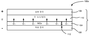
도 1a ~ 도 1n은 본 발명에 따라 제공되는 예시적 쌍극성 저장소자들(100a ~ 100k)의 단면도들이다. 이러한 쌍극성 저장소자들을 형성하기 위한 예시적 공정 상세가 도 3a ~ 도 3f을 참조하여 이하 기술된다.1A-1N are cross-sectional views of exemplary
각 쌍극성 저장소자(100a ~ 100k)는 상부 전극(106)과 하부 전극(108) 사이에 개재된 가역 저항률 전환(RRS) 물질(104)을 포함하는 MIM 스택(102a ~102k) 형태를 취한다. 이하 더욱 기술되는 바와 같이, MIM 스택(102a ~102k) 내에 이를테면 금속층, 금속 산화물층, 금속/금속 산화물층 스택, 등과 같은 하나 이상의 추가의 층들(110)이 채용될 수도 있다.Each
각 MIM 스택(102a ~102k)은 상부 전극(106)/RRS 물질(104) 계면과 하부 전극(108)/RRS 물질(104) 계면 간에 차이들(예를 들면, 일함수, 전자 친화력, 산소 친화력, 계면 층들, 등에서 차이들)에 기인하여 쌍극성 전환을 나타낸다. 이러한 쌍극성 MIM 스택들은 한 전압 극성이 상부 전극(106)과 하부 전극(108) 간에 적용된 상태에선 우선적으로 셋하며, 반대 전압 극성이 상부 전극(106)과 하부 전극(108) 사이에 적용된 상태에선 우선적으로 리셋한다.Each MIM stack 102a-102k differs between the
일부 실시예들에서, MIM 스택들(102a ~ 102k)은 RRS 물질(104)의 양측에 수들, 유형들 및/또는 두께들이 서로 달라 비대칭일 수도 있다.In some embodiments, MIM stacks 102a-102k may be asymmetrical because the numbers, types, and / or thicknesses are different on both sides of
RRS 물질(104)은 예를 들면, HfOX, ZrOX, NiOX, TiOX, TaOX, NbOX, AlXOY, 또 다른 금속 산화물(MOX) 층, 또는 또 다른 적합한 전환 물질을 포함할 수도 있다. 일부 실시예들에서, 상부 전극(106)은 질화티탄, 질화탄탈, 질화텅스텐, 이들의 조합들, Ti/TiN, Ta/TaN, W/WN과 같은 금속/금속 질화물 스택 또는 또 다른 유사한 층; 및 하부 전극(108)은 n+ 실리콘 또는 p+ 실리콘, 고농도 도핑된 게르마늄, 고농도 도핑된 실리콘-게르마늄, 등과 같은 고농도 도핑된 반도체를 포함할 수도 있다. 다른 실시예들에서, 상부 전극(106)은 n+ 실리콘 또는 p+ 실리콘, 고농도 도핑된 게르마늄, 고농도 도핑된 실리콘-게르마늄, 등과 같은 고농도 도핑된 반도체를 포함할 수 있고, 하부 전극(108)은 질화티탄, 질화탄탈, 질화텅스텐, 이들의 조합들, Ti/TiN, Ta/TaN, W/WN과 같은 금속/금속 질화물 스택 또는 또 다른 유사한 층을 포함할 수 있다. 상부 전극(106) 및/또는 하부 전극(108) 용으로 그외 다른 물질들 및/또는 구성들이 사용될 수도 있다.
일부 실시예들에서, 추가의 층(들)(110)은, 예를 들면, 티탄, 티탄 산화물, 탄탈, 탄탈 산화물, 텅스텐, 텅스텐 산화물, 등을 포함할 수 있다. 다른 실시예들에서, 추가의 층(들)(110)은 Ti/TiOX, Zr/ZrOX, Ni/NiOX, Al/AlXOY, Ta/TaOX, Nb/NbOX, Hf/HfOX과 같은 금속/금속 산화물층 스택, 혹은 임의의 적합한 층 스택을 포함할 수 있다.In some embodiments, the additional layer (s) 110 may include, for example, titanium, titanium oxide, tantalum, tantalum oxide, tungsten, tungsten oxide, and the like. In other embodiments, additional layer (s) 110 may comprise Ti / TiO X , Zr / ZrO X , Ni / NiO X , Al / Al X O Y , Ta / TaO X , Nb / NbO X , Hf / Metal / metal oxide layer stacks, such as HfO X , or any suitable layer stack.
본 발명의 쌍극성 MIM 스택들의 동작이 이제 기술된다. 도 1a ~ 도 1b를 참조하면, 쌍극성 MIM 스택(100a)은 저 저항 또는 "셋" 상태(도 1a) 또는 고 저항 또는 "리셋" 상태(도 1b)에 있을 수 있다. 임의의 특정한 이론에 구속되기를 바라지 않지만, RRS 물질(104)은 RRS 물질(104) 내에 산소 빈자리들(112)의 생성 및/또는 제거에 의해 자신의 저항률이 조절되게 할 수도 있을 것으로 생각된다. 일부 실시예들에서, RRS 물질(104) 내에 충분한 수의 산소 빈자리들(112)이 있을 때, 도전성 경로들 또는 필라멘트들이 RRS 물질(104)(도 1a에 도시된 바와 같이)의 전체 폭에 걸쳐 확장할 수 있고 RRS 물질(104)을 통해 저 저항 경로를 생성할 수 있다. 마찬가지로, RRS 물질(104)(도 1b에 도시된 바와 같이)에 걸쳐 확장하고 RRS 물질(104)을 통해 임의의 경로의 저항을 증가시키는 도전성 경로들 또는 필라멘트들을 제거하기 위해 RRS 물질(104)로부터 산소 빈자리들이 제거될 수도 있다. 다른 실시예들에서, 도전성 경로들 또는 필라멘트들은 실제로 형성되지 않을 수 있고, 단지 산소 빈자리 밀도의 증가가 RRS 물질 저항률을 감소시킬 수 있고 산소 빈자리 밀도의 증가는 RRS 물질 저항률을 증가시킬 수 있다.The operation of the bipolar MIM stacks of the present invention is now described. 1A-1B, the
처음 형성되었을 때, RRS 물질(104)은 전형적으로 고 저항률 상태에 있고, RRS 물질(104)을 적합한 극성(이하 더욱 기술되는 바와 같이)의 셋 전압 및 리셋 전압의 인가에 의해 조절될 수 있는 조건에 두기 위해 형성 전압이 인가된다. 형성 전압은 전형적으로 셋 또는 리셋 전압들(예를 들면, 약 14 ~ 16 볼트 대 약 7 ~ 10 볼트)보다 현저하게 크다. 임의의 특정한 이론에 구속되기를 바라지 않지만, 형성 전압의 인가는 RRS 물질(104) 내에 기준적인 수의 산소 빈자리들을 생성할 수 있고, RRS 물질(104) 내에 산소 빈자리들의 수는 RRS 물질(104)의 저항률을 조절하기 위해서 셋 및 리셋 전압들의 인가를 통해 이 기준에 관하여 조절될 수 있다.When initially formed, the
본 발명의 실시예들에서, 추가의 층(들)(110)은 셋 동작(도 1a) 동안에 RRS 물질(104)로부터 산소 이온들을 "게터링(getter)"하여, 산소 이온들이 RRS 물질(104)을 떠나 추가의 층(들)(110)로 이동하기 때문에 RRS 물질(104) 내에 산소 빈자리들(112)을 생성하는 것으로 생각된다. 이것은 RRS 물질(104)을 저 저항률 상태로 전환하게 한다. 마찬가지로, 추가의 층(들)(110)은 리셋 동작(도 1b) 동안에 RRS 물질(104)에 산소 이온들이 시드가 되게 하여, 산소 이온들이 추가의 층(들)(110)에서 RRS 물질(104)로 이동하기 때문에 RRS 물질(104) 내에 산소 빈자리들을 패시베이트(passivate)하는 것으로 생각된다. 이것은 RRS 물질(104)을 고 저항률 상태로 전환하게 한다.In embodiments of the present invention, additional layer (s) 110 “getter” oxygen ions from
본원에서 사용되는 바와 같이, 셋 동작 동안에 자신의 하부 전극을 기준으로 해서 자신의 상부 전극에 인가되는 정의 전압을 채용하는 쌍극성 MIM 스택을 "정 극성" 또는 "정 극성 방위"를 갖는다라고 한다. 마찬가지로, 셋 동작 동안에 자신의 하부 전극을 기준으로 해서 자신의 상부 전극에 인가되는 음의 전압을 채용하는 쌍극성 MIM 스택을 "음 극성" 또는 "음 극성 방위"를 갖는다라고 한다.As used herein, a bipolar MIM stack that employs a positive voltage applied to its upper electrode relative to its lower electrode during a set operation is said to have a "positive polarity" or "positive polarity orientation". Likewise, a bipolar MIM stack that employs a negative voltage applied to its upper electrode with respect to its lower electrode during the set operation is said to have a "negative polarity" or "negative polar orientation".
MIM 스택(102a)은 "정 극성" MIM 스택의 예이다. 예를 들면, MIM 스택(102a)을 저 저항 상태에 셋하기 위해서, 하부 전극(108)을 기준으로 하여 상부 전극(106)에 정의 전압이 인가된다. 이것은 RRS 물질(104) 내에 음의 산소 이온들(O-)이 추가의 층(들)(110) 쪽으로 이동하게 할 수 있다. 산소 이온들이 RRS 물질(104)을 떠날 때, RRS 물질(104) 내에 산소 빈자리들(112)이 형성되어, RRS 물질(104)의 저항률을 낮추고, 어떤 경우들에 있어선, 도 1a에 도시된 바와 같이 RRS 물질(104) 내에 하나 이상의 도전성 경로들 또는 필라멘트들을 생성한다. MIM 스택(102a)을 고 저항 상태에 리셋하기 위해서, 하부 전극(108)을 기준으로 상부 전극(106)에 반대 전압 극성이 인가되는데, 이것은 산소 이온들이 추가의 층(들)(110)에서 RRS 물질(104)로 이동하게 할 수 있다. 이것은 RRS 물질(104) 내에 산소 빈자리들을 패시베이트할 수 있고, 어떤 경우들에 있어선 RRS 물질(104)을 가로질러 확장하는 도전 경로들 또는 필라멘트들을 절단하여 RRS 물질(104)의 저항률을 증가시킨다.MIM stack 102a is an example of a "positive" MIM stack. For example, to set the MIM stack 102a to a low resistance state, a positive voltage is applied to the
도 1c ~ 도 1d는 RRS 물질(104) 및 추가의 층(들)(110)의 위치들이 역전된 "음 극성" MIM 스택(102b)을 도시한다. 이하 기술되는 바와 같이, 상부 전극 물질 및 하부 전극 물질 또한 역전될 수 있다. MIM 스택(102b)은 하부 전극(108)(도 1c)을 기준으로 하여 상부 전극(106)에 음의 전압 극성을 인가함으로써 셋되고, 하부 전극(108)(도 1d)을 기준으로 하여 상부 전극(106)에 정의 전압 극성을 인가함으로써 리셋된다. 본 발명에 따라 제공되는 추가의 MIM 스택들이 이제 도 1e ~ 도 1n을 참조하여 기술된다.1C-1D show “negative polarity” MIM stack 102b with the locations of
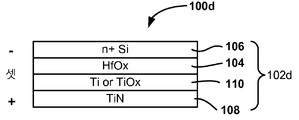
도 1e는 하부 금속 질화물 전극(108), 하부 전극(108) 위에 형성된 금속 또는 금속 산화물층(110), 금속 또는 금속 산화물층(110) 위에 형성된 RRS 물질(104), 및 RRS 물질(104) 위에 형성된 상부 고농도 도핑된 반도체 전극(106)을 가진 제 3 예시적 쌍극성 저장소자(100c)(MIM 스택(102c))의 단면도를 도시한다. MIM 스택(102c)을 저 저항 상태로 "셋"하기 위해서, 하부 전극(108)을 기준으로 상부 전극(106)에 음의 전압이 인가된다. 마찬가지로, MIM 스택(102c)을 고 저항 상태로 "리셋"하기 위해서, 하부 전극(108)을 기준으로 상부 전극(106)에 정의 전압이 인가된다.FIG. 1E illustrates the bottom
일반적으로, 하부 전극(108)은, 예를 들면, 질화티탄, 질화탄탈, 질화텅스텐, 이들의 조합들, Ti/TiN, Ta/TaN, W/WN와 같은 금속/금속 질화물 스택, 또는 또 다른 유사한 장벽층을 포함할 수 있다. 금속 또는 금속 산화물층(110)은, 예를 들면, 티탄, 티탄 산화물, 탄탈, 탄탈 산화물, 텅스텐, 텅스텐 산화물, 또는 또 다른 유사한 층을 포함할 수 있다. RRS 물질(104)은, 예를 들면, HfOX, ZrOX, NiOX, TiOX, TaOX, NbOX 또는 AlXOY 또는 또 다른 적합한 전환 물질을 포함할 수 있다. 상부 전극(106)은 n+ 실리콘 또는 p+ 실리콘과 같은 고농도 도핑된 실리콘, 고농도 도핑된 게르마늄, 고농도 도핑된 실리콘-게르마늄, 등을 포함할 수 있다.In general, the
도 1f는 하부 전극(108)이 질화티탄이고 금속 또는 금속 산화물층(110)이 티탄 또는 티탄 산화물이며, RRS 물질(104)이 하프늄 산화물이고 상부 전극(106)이 n+ 실리콘인, 도 1f에선 MIM 스택(102d)이라고 하는, MIM 스택(102c)의 특정한 예시적 실시예를 도시한 것이다. 예를 들면, 하부 전극(108)(TiN)은 약 10 ~ 60 나노미터, 일부 실시예들에선 약 20 나노미터의 두께를 가질 수 있다. Ti 또는 TiOX 층(110)은 약 0.5 ~ 10 나노미터의 두께, 일부 실시예들에선 약 4 나노미터를 가질 수 있다. TiOX이 채용될 때, x는 약 1.2 ~ 2, 일부 실시예들에선 약 1.5일 수 있다. 하프늄 산화물층(104)은 약 3 ~ 12 나노미터의 두께, 일부 실시예들에선 약 5 나노미터를 가질 수 있고, x는 약 1.2 ~ 2.0, 일부 실시예들에선 약 1.7이다. n+ 실리콘층(106)은 약 10 ~ 100 나노미터의 두께, 일부 실시예들에선 약 20 나노미터를 가질 수 있다. n+ 실리콘층(106)의 도핑 농도는 약 5 x 10¹⁹ ~ 5 x 10²¹ atoms/cm3, 일부 실시예들에선 약 2 x 10²⁰ atoms/cm3일 수 있다. 이외 다른 막 두께들, x 값들 및/또는 도핑 농도들이 사용될 수도 있다. MIM 스택(102d)은 MIM 스택(102c)에 대해 위에 기술된 바와 동일한 전압 극성들을 사용하여 셋 및 리셋된다.FIG. 1F illustrates the MIM in FIG. 1F, wherein the
도 1g ~ 도 1h은 각각 MIM 스택들(102c, 102d)의 "반전된" 버전들을 나타내는 추가의 MIM 스택들(102e, 102f)을 도시한 것이다. 구체적으로, MIM 스택(102e)에서 물질층들의 순서는 MIM 스택(102c)을 기준으로 하여 역전되고, MIM 스택(102f)에서 물질층들의 순서는 MIM 스택(102d)을 기준으로 역전된다. MIM 스택들(102e, 102f)은 하부 전극(108)을 기준으로 정의 전압을 상부 전극(106)에 인가함으로써 저 저항 상태로 "셋"된다. 마찬가지로, MIM 스택(102e 또는 102f)을 고 저항 상태로 "리셋" 하기 위해서, 하부 전극(108)을 기준으로 상부 전극(106)에 음의 전압이 인가된다.1G-1H show
도 1i는 하부 금속 질화물 전극(108), 하부 전극(108) 위에 형성된 금속 산화물층(110a) 및 금속층(110b)을 포함하는 금속/금속 산화물층 스택(110), 금속/금속 산화물층 스택(110) 위에 형성된 RRS 물질(104), 및 RRS 물질(104) 위에 형성된 상부 고농도 도핑된 반도체 전극(106)을 갖는 또 다른 예시적 쌍극성 저장소자(100g)(MIM 스택(102g))의 단면도를 도시한 것이다.FIG. 1I illustrates a metal / metal
임의의 특정한 이론에 구속되기를 바라지 않지만, 이러한 배열에서, 금속층(110b)은 셋 동작 동안에 RRS 물질(104)로부터 산소 이온들을 "게터링"하여, 산소 이온들이 RRS 물질(104)을 떠나 금속층(110b)으로 이동하기 때문에 RRS 물질(104) 내에 산소 빈자리들을 생성하여 RRS 물질(104)을 저 저항률 상태로 전환하게 하는 것으로 생각된다. 마찬가지로, 금속 산화물층(110a)은 리셋 동작 동안에 RRS 물질(104)에 산소 이온들이 시드가 되게 하여, 산소 이온들이 금속 산화물층(110a)에서 RRS 물질(104)로 이동하기 때문에 RRS 물질(104) 내에 산소 빈자리들을 패시베이트하여 RRS 물질(104)을 고 저항률 상태로 전환하게 하는 것으로 생각된다. 일부 실시예들에서, 금속 산화물층(110a)은 버퍼 층으로서 작용하고 다수의 전환 동작들 동안 금속층(110b)의 강한 게터링 특성들에 기인하여 RRS 물질(104)의 계면(들)에의 손상을 감소시킬 수 있다.While not wishing to be bound by any particular theory, in this arrangement,
MIM 스택(100g)을 저 저항 상태로 "셋"하기 위해서, 하부 전극(108)을 기준으로 상부 전극(106)에 음의 전압이 인가된다. 마찬가지로, MIM 스택(100g)을 고 저항 상태로 "리셋" 하기 위해서, 하부 전극(108)을 기준으로 상부 전극(106)에 정의 전압이 인가된다.To “set” the
일반적으로, 하부 전극(108)은, 예를 들면, 질화티탄, 질화탄탈, 질화텅스텐, 이들의 조합들, 금속/금속 질화물 스택으로서 이를테면 Ti/TiN, Ta/TaN, W/WN, 또는 또 다른 유사한 장벽층을 포함할 수 있다. 금속/금속 산화물층 스택(110)은, 예를 들면, Ti/TiOX, Zr/ZrOX, Ni/NiOX, A1/AlX0Y, Ta/TaOX, Nb/NbOX, Hf/HfOX 또는 또 다른 유사한 층 스택을 포함할 수 있다. RRS 물질(104)은, 예를 들면, HfOX, ZrOX, NiOX, TiOX, TaOX, NbOX 또는 AlXOY 또는 또 다른 적합한 전환 물질을 포함할 수 있다. 상부 전극(106)은 n+ 실리콘, p+ 실리콘, 고농도 도핑된 게르마늄, 고농도 도핑된 실리콘-게르마늄, 등을 포함할 수 있다.Generally, the
일부 실시예들에서, 금속/금속-산화물층 스택(110)은 RRS 물질(104)에 대해 채용되는 것과는 다른 물질로부터 형성될 수 있다. 예를 들면, Ti/TiOX 층 스택은 HfOX, ZrOX, NiOX, TaOX, NbOX 또는 AlXOY 전환 물질과 함께 채용될 수 있다. Zr/ZrOX 층 스택은 HfOX, NiOX, TiOX, TaOX, NbOX 또는 AlXOY 전환 물질과 함께 사용될 수 있다. Ni/NiOX 층 스택은 HfOX, ZrOX, TiOX, TaOX, NbOX 또는 AlXOY 전환 물질과 함께 사용될 수 있다. Al/AlX0Y 층 스택은 HfOX, ZrOX, NiOX, TiOX, TaOX, 또는 NbOX 전환 물질과 함께 채용될 수 있다. Ta/TaOX 층 스택은 HfOX, TiOX, ZrOX, NiOX, NbOX 또는 AlXOY 전환 물질과 함께 채용될 수도 있다. Nb/NbOX 층 스택은 HfOX, TiOX, ZrOX, NiOX, TaOX 또는 AlXOY 전환 물질과 함께 채용될 수 있다. Hf/HfOX 층 스택은 NbOX, TiOX, ZrOX, NiOX, TaOX 또는 AlXOY 전환 물질과 함께 채용될 수 있다.In some embodiments, metal / metal-
다른 실시예들에서, 금속/금속 산화물층 스택(110)은 RRS 물질(104)에 대해 채용된 것과 유사한 물질로부터 형성될 수 있다. 예를 들면, Ti/TiOX 층 스택은 TiOX 전환 층과 함께 채용될 수 있다. 그러나, 이러한 실시예들에서, 층 스택의 금속 산화물은 전환 물질(예를 들면, 비정질 대 결정구조)의 것과 비교해서 다른 결정구조 또는 다른 특성을 가질 수 있다. 금속/금속-산화물층 스택(110)의 금속 산화물층은 전환 물질 내에 산소 빈자리들의 형성/제거가 더 제어가능하고 및/또는 반복가능할 수 있게 하여 전환 물질의 내구성/지속성을 개선할 수 있는 "버퍼"층으로서 작용할 수 있는 것으로 생각된다.In other embodiments, metal / metal
도 1j는 하부 전극(108)이 질화티탄이고, 금속/금속 산화물층 스택(110)이 티탄 위에 티탄 산화물이고, RRS 물질(104)이 하프늄 산화물이고 상부 전극(106)이 n+ 실리콘인, 도 1j에선 MIM 스택(102h)이라고 하는, MIM 스택(102g)의 특정한 예시적 실시예를 도시한 것이다. 예를 들면, 하부 전극(108)(TiN)은 약 10 ~ 60 나노미터의 두께, 일부 실시예들에선 약 20 나노미터를 가질 수 있다. Ti층(110b)은 약 0.5 ~ 10 나노미터의 두께, 일부 실시예들에선 약 4 나노미터를 가질 수 있다. TiOX 층(110a)은 약 0.5 ~ 6 나노미터의 두께, 및 일부 실시예들에선 약 1 나노미터를 가질 수 있고, x는 약 1.2 ~ 2.0, 일부 실시예들에선 약 1.5일 수 있다. 하프늄 산화물층(104)은 약 3 ~ 12 나노미터의 두께, 실시예들에선 약 5 나노미터를 가질 수 있고, x는 약 1.2 ~ 2, 일부 실시예들에서 약 1.7일 수 있다. n+ 실리콘 층(106)은 약 10 ~ 100 나노미터의 두께, 일부 실시예들에서 약 20 나노미터를 가질 수 있다. n+ 실리콘 층(106)의 도핑 농도는 약 5 x 10¹⁹ ~ 5 x 10²¹ atoms/cm3, 일부 실시예들에서 약 2 x 10²⁰ atoms/cm3일 수 있다. 이외 다른 막 두께들, x 값들 및/또는 도핑 농도들이 사용될 수도 있다. MIM 스택(102h)은 MIM 스택(102g)에 대해 위에 기술된 바와 동일한 극성들을 사용하여 셋 및 리셋된다.FIG. 1J shows that the
도 1k ~ 도 1l은 각각 MIM 스택들(102g, 102h)의 "반전된" 버전들을 나타내는 추가의 MIM 스택들(102i, 102j)을 도시한 것이다. 구체적으로, MIM 스택(102i)에서 물질층들의 순서는 MIM 스택(102g)을 기준으로 하여 역전되고, MIM 스택(102j)에서 물질층들의 순서는 MIM 스택(102h)을 기준으로 해서 역전된다. MIM 스택들(102i, 102j)은 하부 전극(108)을 기준으로 정의 전압을 상부 전극(106)에 인가함으로써 저 저항 상태로 "셋"된다. 마찬가지로, MIM 스택(102i 또는 102j)을 고 저항 상태로 "리셋"하기 위해서, 하부 전극(108)을 기준으로 상부 전극(106)에 음의 전압이 인가된다.1K-1L show
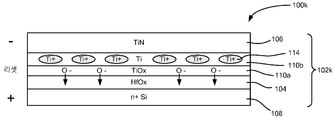
도 1m ~ 도 1n은 도 1l의 MIM 스택(102j)과 유사한 MIM 스택(102k)의 특정한 실시예를 도시한다. MIM 스택(102k)을 가진 테스트 웨이퍼들 상에서, TEM 이미지들은 HfOX 및 TiOX 층들(104, 110a) 사이에 뚜렷한 계면을 나타낸다. TiOX 및 Ti층들(110a, 110b) 간에 계면은 덜 뚜렷한 것으로 나타나고, 비정질 및 결정구조들의 혼합이 TiOX/Ti층 스택(110) 내에서 관찰된다. 예를 들면, 일부 테스트 샘플들에서, 이를테면 TiOX 및/또는 HfOX층들(110a 및/또는 104)로부터 Ti층(110b)에 산소가 확산하여 Ti가 농후한 섬(island)들(114)(예를 들면, 금속 산화물에 의해 둘러싸인 금속 농후 영역들)을 형성할 수 있기 때문에 어떠한 순수한 Ti층(110b)도 존재하지 않는 것으로 나타난다. TiN층(106)으로부터 TiOX층(110a) 및/또는 Ti층(110b)에 질소가 확산할 수도 있다. 사실, 일부 실시예들에서, 아마도 HfOX층(104)에서 Ti층으로 산소 확산에 기인하여, TiOX층이 없이 HfOX층(104) 상에 두꺼운(예를 들면, 약 8 이상의 나노미터) Ti층이 증착될 때 도 1m 및/또는 도 1n의 MIM 스택(102k)과 유사한 구조가 관찰되었다.1M-1N illustrate a particular embodiment of a
임의의 특정한 이론에 구속되기를 바라지 않지만, 이러한 배열에서, Ti층(110b)의 Ti+ 섬들(114)은 셋 동작 동안에 RRS 물질(104)로부터 산소 이온들을 "게터링"하여, 산소 이온들이 RRS 물질(104)을 떠나 Ti층(110b)으로 이동하기 때문에 RRS 물질(104) 내에 산소 빈자리들을 생성하여 RRS 물질(104)을 저 저항률 상태로 전환하게 하는 것으로 생각된다(도 1m). 마찬가지로, TiOX층(110a)은 리셋 동작 동안에 RRS 물질(104)에 산소 이온들이 시드가 되게 하여, 산소 이온들이 TiOX층(110a)에서 RRS 물질(104)로 이동하기 때문에 RRS 물질(104) 내에 산소 빈자리들을 패시베이트하여 RRS 물질(104)을 고 저항률 상태로 전환하게 하는 것으로 생각된다. MIM 스택들(102a ~ 102k)을 위한 형성 전압, 셋 전압 및 리셋 전압에 대한 적합한 값들은 사용되는 물질들의 유형들 및/또는 두께들과 같은 다수의 인자들에 따른다. 일부 실시예들에서, 양의 방위로 놓인 MIM 스택들에 대해서, 약 +14 내지 +16 볼트 또는 그 이상의 형성전압, 약 +9 내지 +11 볼트의 셋 전압, 및/또는 약 -7 내지 -8 볼트의 리셋 전압이 사용될 수 있다. 마찬가지로, 음의 방위로 놓인 MIM 스택들에 대해서, 약 -14 내지 -16 볼트 또는 그 이상의 형성전압, 약 -9 내지 -11 볼트의 셋 전압, 및/또는 약 +7 내지 +8 볼트의 리셋 전압이 사용될 수 있다. 이외 어떤 다른 적합한 형성전압, 셋 전압 및/또는 리셋 전압이 채용될 수 있다.While not wishing to be bound by any particular theory, in this arrangement, the Ti +
위에 MIM 스택들(102a ~ 102k)은 저-저항 셋 상태들 및 고-저항 리셋 상태들을 갖는 것으로서 기술되었다. 다른 실시예들에서, MIM 스택들(102a ~ 102k)은 고 저항 셋 상태들 및 저-저항 리셋 상태들을 가질 수 있다.The MIM stacks 102a-102k have been described as having low-resistance set states and high-resistance reset states. In other embodiments, MIM stacks 102a-102k may have high resistance set states and low resistance reset states.
발명의Invention 예시적Illustrative 메모리 셀Memory cell
도 2a는 본 발명에 따른 예시적 메모리 셀(200)의 개요도이다. 메모리 셀(200)은 스티어링 소자(204)에 결합된 MIM 스택(102)을 포함한다. MIM 스택(102)은 도 1a 내지 도 1n에 관련하여 앞에서 기술된 바와 같이, 2 이상의 상태들 간에 가역적으로 전환될 수 있는 저항률을 가진 RRS 물질(104)(별도로 도시되지 않았음)을 포함한다.2A is a schematic diagram of an
스티어링 소자(204)는 박막 트랜지스터, 다이오드, 금속-절연체-금속 터널링 전류 장치, 펀치 스루 다이오드, 쇼트키-다이오드, 혹은 MIM 스택(102)에 걸리는 전압 및/또는 이를 통하는 전류 흐름을 선택적으로 제한시킴으로써 비-오믹 도전(non-ohmic conduction)을 나타내는 또 다른 유사한 스티어링 소자를 포함할 수 있다. 따라서, 메모리 셀(200)은 2차원 혹은 3차원 메모리 어레이의 일부로서 사용될 수 있고 데이터는 어레이 내 다른 메모리 셀들의 상태에 영향을 미침이 없이 메모리 셀(200)에 기입될 수 있고 및/또는 이로부터 판독될 수 있다. 일부 실시예들에서, 스티어링 소자(204)는 생략될 수도 있고, 메모리 셀(200)은 원격에 위치된 스티어링 소자와 함께 사용될 수도 있다.The
메모리 셀들 및 메모리 어레이들의 예시적 실시예들Example Embodiments of Memory Cells and Memory Arrays
도 2b는 스티어링 소자(204)가 다이오드인 본 발명에 따른 메모리 셀(200)의 예시적 실시예의 간략화한 사시도이다. 메모리 셀(200)은 제 1 도체(202a)와 제 2 도체(202b) 사이에 다이오드(204)와 직렬로 결합된 MIM 스택(102)(RRS 물질(104)을 가진)을 포함한다.2B is a simplified perspective view of an exemplary embodiment of a
도 1a ~ 도 1n에 관련하여 위에 기술된 바와 같이, MIM 스택(102)은 메모리 셀(200)을 위한 가역 저항-전환 소자로서 작용할 수 있다. MIM 스택(102)은 도 1a ~ 도 1n의 MIM 스택들(102a ~ 102k) 중 어느 것, 혹은 이외 어떤 다른 적합한 MIM 스택과 유사할 수 있고, RRS 물질(104)을 둘러싸고 MIM 스택(102)을 위한 상부 및 하부 전극들로서 작용하는 상부 도전층(106) 및 하부 도전층(108)을 포함할 수 있다. 금속층, 금속 산화물층, 금속/금속 산화물층 스택, 등과 같은 하나 이상의 추가의 층들(110)이 앞에 기술된 바와 같은 MIM 스택(102) 내에 채용될 수도 있다.As described above with respect to FIGS. 1A-1N, the
일부 실시예들에서, MIM 스택(102)과 다이오드(204) 사이에 장벽층(206)이 형성될 수도 있고, MIM 스택(102)과 제 2 도체(202b) 사이에 장벽층(208)이 형성될 수도 있다. 추가의 장벽층(210)이 다이오드(204)와 제 1 도체(202a) 사이에 형성될 수 있다. 장벽층들(206, 208, 210)은 티탄, 질화티탄, 탄탈, 질화탄탈, 텅스텐, 질화텅스텐, 몰리브덴, 이들의 조합들, 또는 또 다른 유사한 장벽층을 포함할 수 있다. 장벽층(208)은 제 2 도체(202b)로부터 혹은 이의 부분으로부터 분리될 수 있고 장벽층(210)은 제 1 도체(202a)로부터 혹은 이의 부분으로부터 분리될 수 있다.In some embodiments, a
다이오드(204)는 다이오드의 p-영역 위에 n-영역을 갖고 위쪽으로 향하든지 아니면 다이오드의 n-영역 위에 p-영역을 갖고 아래쪽을 향하든지 간에, 수직 다결정질 p-n 혹은 p-i-n 다이오드, p-n-p 또는 n-p-n 펀치 스루 다이오드, 쇼트키 다이오드, 등과 같은 임의의 적합한 다이오드를 포함할 수 있다. 다이오드(204)의 예시적 실시예들을 이하 도 3a 내지 도 3d를 참조하여 기술한다.
도 2b의 실시예에서, MIM 스택(102)은 다이오드(204) 위에 위치된다. 그러나, 도 2c에 도시된 바와 같이, MIM 스택(102)은 대안적으로 다이오드(204) 밑에 위치될 수도 있다.In the embodiment of FIG. 2B, the
제 1 도체(202a) 및/또는 제 2 도체(202b)는 이를테면 텅스텐, 임의의 적합한 금속, 고농도 도핑된 반도체 물질, 도전성 실리사이드, 도전성 실리사이드-게르마나이드, 도전성 게르마나이드, 매우 도전성의 탄소, 등과 같은 임의의 적합한 도전성 물질을 포함할 수 있다. 도 2a의 실시예에서, 제 1 도체(202a) 및/또는 제 2 도체(202b)는, 각각, 라인 또는 레일(rail) 형상이고 서로 다른 방향들(예를 들면, 서로 실질적으로 수직하게)로 확장한다. 이외 다른 도체 형상들 및/또는 구성들이 사용될 수도 있다. 일부 실시예들에서, 장치 성능을 개선하고 및/또는 장치 제조에 도움이 되게 장벽층들, 부착층들, 반반사 코팅들 및/또는 등(도시되지 않음)이 제 1 도체(202a) 및/또는 제 2 도체(202b)에 사용될 수도 있다.The
도 2d는 도 2a 또는 도 2b의 메모리 셀들(200)과 같은 복수의 메모리 셀들(200)로부터 형성된 제 1 메모리 레벨(212)의 부분을 간략화한 사시도이다. 간략성을 위해서, RRS 물질(104), 도전성 층들(106, 108), 추가의 층(들)(110), 다이오드(204), 및 장벽층들(206, 208, 210)은 개별적으로 도시되지 않았다. 메모리 어레이(212)는 복수의 비트라인들(제 2 도체들(202b)) 및 복수의 메모리 셀들이 결합되는(도시된 바와 같이) 워드라인들(제 1 도체들(202a))을 포함하는 "교차-점" 어레이이다. 복수 레벨들의 메모리와 같이, 그외 메모리 어레이 구성들이 사용될 수도 있다.FIG. 2D is a simplified perspective view of a portion of a
도 2e는 제 2 메모리 레벨(218) 밑에 위치된 제 1 메모리 레벨(216)을 포함하는 모노리식 3차원 어레이(214a)의 부분을 간략화한 사시도이다. 메모리 레벨들(216, 218) 각각은 교차-점 어레이 내 복수의 메모리 셀들(200)을 포함한다. 당업자들은 추가의 층들(예를 들면, 레벨간 유전체)이 제 1 메모리 레벨(216)과 제 2 메모리 레벨(218) 사이에 있을 수 있지만 그러나 간략성을 위해 도 2e엔 도시되지 않았음을 알 것이다. 추가된 레벨들의 메모리와 같이, 그외의 메모리 어레이 구성들이 사용될 수도 있다.2E is a simplified perspective view of a portion of a monolithic three
도 2e의 실시예에서, p-i-n 다이오드와 같은 쌍극성 스티어링 소자가 각 메모리 셀(200) 내에 채용될 때, 모든 다이오드들은 다이오드들의 하부 혹은 상부 상에 p-도핑된 영역을 갖는 p-i-n 다이오드들이 채용되는지 여부에 따라 위쪽 혹은 아래쪽과 같이 같은 방향(동일 "스티어링 소자" 극성 방위를 갖는)으로 "향할" 수 있어, 다이오드 제조를 단순화한다. 본 발명에 따라, 모든 쌍극성 MIM 스택들(102)은 도 2e의 메모리 어레이(214a)에서 모든 메모리 레벨들에 걸쳐 동일한 극성 방위를 가질 수도 있다. 즉, 메모리 어레이(214a) 내 각 MIM 스택(102)은 셋 동작 동안 자신의 하부 전극을 기준으로 각 MIM 스택(102)의 상부 전극에 정의 전압이 인가되게 양의 방위로 놓이거나, 셋 동작 동안 자신의 하부 전극을 기준으로 각 MIM 스택(102)의 상부 전극에 음의 전압이 인가되게, 음의 방위로 놓여질 수 있다. 이것은 MIM 스택 제조를 단순화시킨다.In the embodiment of FIG. 2E, when a bipolar steering element, such as a pin diode, is employed in each
일부 실시예들에서, 메모리 레벨들은 모든 목적들을 위해 전체를 참조로서 본원에 포함시키는 "High-Density Three-Dimensional Memory Cell" 명칭의 미국특허 6,952,030에 기술된 바와 같이 형성될 수 있다. 예를 들면, 제 1 메모리 레벨의 제 2 (상부) 도체들은 도 2f에 도시된 바와 같이 제 1 메모리 레벨 위에 위치되는 제 2 메모리 레벨의 제 1 (하부) 도체들로서 사용될 수도 있다. 이러한 실시예들에서, 모든 목적들을 위해 전체를 참조로서 본원에 포함시키는 "Large Array Of Upward Pointing P-I-N Diodes Having Large And Uniform Current" 명칭으로 2007년 3월 27일에 출원된 미국특허출원번호 11/692,151("'151 출원")에 기술된 바와 같이, 이웃한 메모리 레벨들 상에 다이오드들은 바람직하게 서로 반대되는 방향들을 향한다. 예를 들면, 도 2f에 메모리 어레이(214b)에 도시된 바와 같이, 제 1 메모리 레벨(216)의 다이오드들은 화살표(D1)로 나타낸 바와 같이 위로 향하는 다이오드들일 수 있고(예를 들면, 다이오드들의 하부에 p 영역들을 가진), 제 2 메모리 레벨(218)의 다이오드들은 화살표(D2)로 나타낸 바와 같이 아래로 향하는 다이오드들일 수 있으며(예를 들면, 다이오드들의 하부에 n 영역들을 가진), 혹은 그 반대일 수도 있다.In some embodiments, memory levels may be formed as described in US Pat. No. 6,952,030, entitled “High-Density Three-Dimensional Memory Cell,” which is incorporated herein by reference in its entirety for all purposes. For example, second (top) conductors of the first memory level may be used as first (bottom) conductors of the second memory level located above the first memory level as shown in FIG. 2F. In such embodiments, US patent application Ser. No. 11 / 692,151, filed March 27, 2007, entitled "Large Array Of Upward Pointing PIN Diodes Having Large And Uniform Current", which is hereby incorporated by reference in its entirety for all purposes. As described in ("'151 application"), the diodes on neighboring memory levels are preferably directed in opposite directions. For example, as shown in
본 발명에 따라, 도 2f에서와 같이 메모리 레벨들 간에 도체들이 공유되는 실시예들에서, MIM 스택들(102)은 메모리 레벨 내에 동일 전압 극성 방위를 갖지만 이웃한 메모리 레벨들 간에는 반대 전압 극성을 갖게 배열된다. 예를 들면, 제 1 메모리 레벨(216)의 MIM 스택들(102)은 양의 방위로 놓여질 수 있고, 제 2 메모리 레벨(218)의 MIM 스택들(102)은 음의 방위로 놓여질 수 있고, 그 반대로도 될 수 있다. 일부 실시예들에서, 다이오드들(204)는 MIM 스택들(102)의 셋 동작들 동안에 역바이어스되게 하는 방위로 놓여질 수 있다. 대안적으로, 다이오드들(204)은 MIM 스택들(102)의 셋 동작들 동안에 순방향 바이어스되게 하는 방위로 놓여질 수 있다.According to the present invention, in embodiments in which conductors are shared between memory levels as in FIG. 2F, MIM stacks 102 have the same voltage polarity orientation within the memory level but opposite voltage polarity between neighboring memory levels. Are arranged. For example, the MIM stacks 102 of the
모노리식 3차원 메모리 어레이는 개재되는 어떠한 기판들도 없이 복수의 메모리 레벨들이 웨이퍼와 같은 단일 기판 위에 형성되는 어레이이다. 한 메모리 레벨을 형성하는 층들은 현존 레벨 혹은 레벨들의 층들 상에 직접 증착 혹은 성장된다. 반대로, 적층된 메모리들은 "Three Dimensional Structure Memory" 명칭의 Leedy의 미국특허 5,915,167에서와 같이, 개별적 기판들 상에 메모리 레벨들을 형성하고 메모리 레벨들을 서로 수직으로 부착함으로써 구성되었다. 기판들은 본딩 전에 얇게 하거나 메모리 레벨들로부터 제거될 수도 있는데, 그러나 메모리 레벨들이 초기에 개별적 기판들 상에 형성되기 때문에, 이러한 메모리들은 진정한 모노리식 3차원 메모리 어레이들이 아니다.A monolithic three dimensional memory array is an array in which a plurality of memory levels are formed on a single substrate, such as a wafer, without any intervening substrates. Layers forming a memory level are deposited or grown directly on existing levels or layers of levels. In contrast, stacked memories were constructed by forming memory levels on individual substrates and attaching the memory levels vertically to each other, as in US Pat. No. 5,915,167 to Leedy, entitled “Three Dimensional Structure Memory”. The substrates may be thinned or removed from the memory levels before bonding, but since the memory levels are initially formed on individual substrates, these memories are not true monolithic three dimensional memory arrays.
예시적인 적층된 메모리 셀들Example Stacked Memory Cells
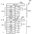
도 3a는 본 발명에 따라 제공된 제 1 메모리 셀 스택(300a)의 단면도이다. 메모리 셀 스택(300a)은 제 1 메모리 셀(200-1) 위에 형성된 제 1 메모리 셀(200-1) 및 제 2 메모리 셀(200-2)을 포함한다. 도 3a에 도시된 바와 같이, 제 1 및 제 2 메모리 셀들(200-1, 200-2)은 제 1 메모리 셀(200-1)의 상부 도전성 레일 및 제 2 메모리 셀(200-2)의 하부 도전성 레일 둘 다로서 작용하는 공통의 워드라인(302)을 공유한다. 다른 실시예들에서, 제 1 및 제 2 메모리 셀들(200-1, 200-2)은 워드라인이 아니라 비트라인을 공유할 수도 있다. 도 2d ~ 도 2f에 기술된 바와 같이 각 메모리 레벨(예를 들면, 메모리 셀들(200-1 및/또는 200-2)의 좌측 및/또는 우측에)에 추가의 메모리 셀들(도시되지 않음)이 제공될 수도 있다.3A is a cross-sectional view of a first
도 3a를 참조하면, 제 1 메모리 셀(200-1)은 비트라인(202a)과 워드라인(302) 사이에서 제 1 다이오드(204-1)와 직렬로 결합된 제 1 MIM 스택(102-1)을 포함한다. 제 1 MIM 스택(102-1)은 제 1 MIM 스택(102-1)을 셋하기 위해 비트라인(202a)을 기준으로 해서 워드라인(302)에 인가되는 정의 전압이 채용될 수 있게 정 극성 방위를 갖는다. 제 1 다이오드(204-1)는 이러한 셋 동작 동안에 역바이어스되게 하는 방위로 놓여진다. 다른 실시예들에서, 제 1 다이오드(204-1)는 제 1 MIM 스택(102-1) 상에 셋 동작이 수행되는 동안 순방향 바이어스되게 하는 방위로 놓여질 수도 있다.Referring to FIG. 3A, the first memory cell 200-1 is a first MIM stack 102-1 coupled in series with the first diode 204-1 between the
제 2 메모리 셀(200-2)은 워드라인(302)과 비트라인(202b)과 사이에서 제 2 다이오드(204-2)와 직렬로 결합된 제 2 MIM 스택(102-2)을 포함한다. 제 2 MIM 스택(102-2)은 제 2 MIM 스택(102-2)을 셋하기 위해 비트라인(202b)을 기준으로 해서 워드라인(302)에 인가되는 정의 전압이 채용될 수 있게 음 극성 방위를 갖는다. 제 2 다이오드(204-2)는 이러한 셋 동작 동안에 역바이어스되게 하는 방위로 놓여진다. 다른 실시예들에서, 제 2 다이오드(204-2)는 제 2 MIM 스택(102-2) 상에 셋 동작이 수행되는 동안 순방향 바이어스되게 하는 방위로 놓여질 수도 있다.The second memory cell 200-2 includes a second MIM stack 102-2 coupled in series with the second diode 204-2 between the
도 3a로부터 알 수 있는 바와 같이, 제 1 MIM 스택(102-1)은 제 1 극성 방위를 가지며, 제 2 MIM 스택(102-2)은 제 1 MIM 스택(102-1)을 기준으로 하여 제 2의 반대 극성 방위를 갖는다. 마찬가지로, 제 1 다이오드(204-1)은 제 1 극성 방위를 가지며, 제 2 다이오드(204-2)은 제 1 다이오드(204-1)를 기준으로 하여 제 2의 반대 극성 방위를 갖는다.As can be seen from FIG. 3A, the first MIM stack 102-1 has a first polarity orientation, and the second MIM stack 102-2 is based on the first MIM stack 102-1. Has the opposite polarity orientation of 2. Similarly, the first diode 204-1 has a first polarity orientation and the second diode 204-2 has a second opposite polarity orientation relative to the first diode 204-1.
제 1 MIM 스택(102-1) 및 제 2 MIM 스택(102-2)은 앞에 기술된 MIM 스택들(102a ~ 102k) 중 어느 것, 혹은 이외 어떤 다른 적합한 MIM 스택 및/또는 쌍극성 저장소자를 포함할 수 있다. 도 3a에서, 제 1 MIM 스택(102-1) 및 제 2 MIM 스택(102-2)은 각각 MIM 스택(102h)(도 1j) 및 MIM 스택(102j)(도 1l)과 유사한 것으로서 도시되었다. The first MIM stack 102-1 and the second MIM stack 102-2 include any of the MIM stacks 102a-102k described above, or any other suitable MIM stack and / or bipolar reservoir. can do. In FIG. 3A, the first MIM stack 102-1 and the second MIM stack 102-2 are shown as similar to the
제 1 다이오드(204-1) 및 제 2 다이오드(204-2)는 임의의 2단자 비선형 스티어링 소자로서, 이를테면 p-n 또는 p-i-n 접합 다이오드, 펀치 스루 다이오드, 터널링 산화물 장치, 쇼트키 다이오드, 등을 포함할 수 있다. 도 3a에서, 제 1 다이오드(204-1) 및 제 2 다이오드(204-2)는 p-i-n 접합 다이오드들인 것으로서 도시되었다. 도 3a의 것과 같은 도체 공유 실시예에서 쌍극성 스티어링 소자들이 채용될 때, 다이오드들의 극성은 도시된 바와 같이 메모리 레벨들 간에 교번된다. 그러나, 펀치 스루 다이오드들와 같은 단극성 스티어링 소자들이 채용될 때, 다이오드들은 도 3b의 메모리 셀 스택(300b)에 보인 바와 같이 메모리 레벨 간에 같은 방위로 놓여질 수 있다.The first diode 204-1 and the second diode 204-2 are any two-terminal nonlinear steering elements such as pn or pin junction diodes, punch through diodes, tunneling oxide devices, Schottky diodes, and the like. Can be. In FIG. 3A, the first diode 204-1 and the second diode 204-2 are shown as p-i-n junction diodes. When bipolar steering elements are employed in a conductor sharing embodiment such as that of FIG. 3A, the polarities of the diodes are alternated between memory levels as shown. However, when unipolar steering elements such as punch-through diodes are employed, the diodes can be placed in the same orientation between memory levels as shown in
도 3a를 참조하면, 제 1 메모리 셀(200-1)은 비트라인(202a)을 포함한다. 비트라인(202a)은 텅스텐 또는 또 다른 적합한 금속, 고농도 도핑된 반도체 물질, 도전성 실리사이드, 도전성 실리사이드-게르마나이드, 도전성 게르마나이드, 등과 같은 약 200 내지 약 2500 옹스트롬의 임의의 적합한 도전성 물질일 수 있다. 일부 실시예들에서, 복수의 비트라인들(202a)(예를 들면, 도 2d ~ 도 2f 참조)은 실질적으로 평행한, 실질적으로 공면(co-planar)의 비트라인들(202a)로서 형성될 수 있다. 다른 도체 폭들 및/또는 간격들이 사용될 수도 있을지라도, 비트라인들(202a)에 대한 예시적 폭들 및/또는 비트라인들(202a) 사이의 간격들은 약 200 내지 약 2500 옹스트롬의 범위이다. 비트라인들(202a)은 이산화실리콘, 실리콘 질화물, 실리콘 옥시나이트라이드, 저 K 유전체, 등과 같은 유전체 물질 (도시되지 않음) 및/또는 다른 유전체 물질들에 의해 서로로부터 분리될 수 있다.Referring to FIG. 3A, the first memory cell 200-1 includes a
장벽층(210)은 비트라인(202a) 상에 형성된다. 장벽층(210)은 약 20 내지 약 500 옹스트롬, 및 바람직하게 약 100 옹스트롬의 질화티탄 또는 질화탄탈, 질화텅스텐, 텅스텐, 몰리브덴과 같은, 또 다른 적합한 장벽층, 하나 이상의 장벽층들의 조합들, 티탄/질화티탄, 탄탈/질화탄탈 또는 텅스텐/질화텅스텐 스택들, 등과 같은 다른 층들과 조합한 장벽층들일 수 있다. 이외 다른 장벽층 물질들 및/또는 두께들이 채용될 수도 있다.The
다이오드(204-1)을 형성하기 위해 사용되는 반도체 물질이 장벽층(210) 상에 형성된다. 도 3a의 실시예에서, 다이오드(204-1)는 폴리실리콘, 다결정질 실리콘-게르마늄 합금, 폴리게르마늄 혹은 이외 어떤 다른 적합한 물질과 같은 다결정질 반도체 물질로부터 형성된다. 예를 들면, 고농도 도핑된 비정질 또는 다결정질 p+ 실리콘층(204-1a)이 장벽층(210) 상에 증착될 수도 있다. p+ 실리콘 층(204-1a)을 증착하기 위해 CVD 또는 또 다른 적합한 공정이 채용될 수 있다. 적어도 일 실시예에서, 예를 들면, 약 1021cm-3의 도핑 농도를 가진 약 100 내지 약 1000 옹스트롬, 바람직하게 약 100 옹스트롬의 p+ 실리콘으로부터 p+ 실리콘층(204-1a)이 형성될 수 있다. 이외 다른 층 두께들 및/또는 도핑 농도들이 사용될 수도 있다. 예를 들면, 증착 동안 어셉터 기체를 플로우(flow)함으로써 인 시튜(in situ)로, 혹은 예를 들면, 주입을 통해 엑스 시튜(ex situ)로, p+ 실리콘 층(204-1a)이 도핑될 수도 있다.A semiconductor material used to form the diode 204-1 is formed on the
p+ 실리콘 층(204-1a) 증착 후에, p+ 실리콘 층(204-1a) 위에 저농도 도핑된, 진성 및/또는 비의도적으로 도핑된 비정질 또는 다결정질 실리콘 층(204-1b)이 형성될 수 있다. 진성 실리콘 층(204-1b)을 증착하기 위해 CVD 또는 또 다른 적합한 증착 방법이 채용될 수도 있다. 적어도 일 실시예에서, 진성 실리콘 층(204-1b)은 두께가 약 500 내지 약 4800 옹스트롬, 바람직하게 약 2500 옹스트롬일 수 있다. 이외 다른 진성 층 두께들이 사용될 수도 있다.After deposition of the p + silicon layer 204-1a, a lightly doped, intrinsically and / or unintentionally doped amorphous or polycrystalline silicon layer 204-1b may be formed over the p + silicon layer 204-1a. CVD or another suitable deposition method may be employed to deposit intrinsic silicon layer 204-1b. In at least one embodiment, intrinsic silicon layer 204-1b may be about 500 to about 4800 angstroms thick, preferably about 2500 angstroms thick. Other intrinsic layer thicknesses may be used.
추가의 실리콘은 이온 주입에 의해 증착되고 도핑될 수도 있고 혹은 n+ 실리콘 층(204-1c)을 형성하기 위한 증착 동안 인 시튜로 도핑될 수 있다. 또한, 일부 실시예들에서, 확산 공정이 채용될 수도 있다. 적어도 일 실시예에서, 결과적인 n+ 실리콘층(204-1c)은 약 100 내지 약 1000 옹스트롬, 바람직하게 약 100 옹스트롬의 두께를 가질 수 있고, 약 1021 cm-3의 도핑 농도를 가질 수 있다. 이외 다른 층 두께들 및/또는 도핑 농도들이 사용될 수도 있다.Additional silicon may be deposited and doped by ion implantation or doped in situ during deposition to form n + silicon layer 204-1c. In addition, in some embodiments a diffusion process may be employed. In at least one embodiment, the resulting n + silicon layer 204-1c may have a thickness of about 100 to about 1000 angstroms, preferably about 100 angstroms, and may have a doping concentration of about 10 21 cm −3 . Other layer thicknesses and / or doping concentrations may be used.
n+ 실리콘 층(204-1c)의 형성에 이어, n+ 실리콘 층(204-1c) 상에 실리사이드-형성 금속층 스택(206)이 증착될 수 있다. 예시적 실리사이드-형성 금속들은 스퍼터 또는 아니면 증착된 티탄 또는 코발트를 포함한다. 일부 실시예들에서, 실리사이드-형성 금속층 스택(206)은 약 1 ~ 4 나노미터의 티탄 및 약 15 ~ 25 나노미터의 질화티탄으로부터 형성된다. 이외 다른 실리사이드-형성 금속층 물질들 및/또는 두께들이 사용될 수도 있다.Following formation of the n + silicon layer 204-1c, a silicide-forming
Ti와 같은 실리사이드-형성 금속의 n+ 영역(204-1c)과의 반응에 의해 실리사이드 영역을 형성하기 위해 급속 열 어닐링("RTA") 단계가 수행될 수 있다. 일부 실시예들에서, RTA는 실리사이드-형성 금속의 전부 또는 일부를 소비하면서, 실리사이드-형성 금속 및 다이오드(204)의 증착된 실리콘이 실리사이드층을 형성하기 위해 상호작용하게, 약 1분 동안 약 540℃에서 수행될 수 있다.A rapid thermal annealing (“RTA”) step may be performed to form the silicide region by reaction of the silicide-forming metal, such as Ti, with the n + region 204-1c. In some embodiments, the RTA consumes all or a portion of the silicide-forming metal, while the silicide-forming metal and the deposited silicon of the
모든 목적들을 위해 전체를 참조로서 본원에 포함시키는 "Memory Cell Comprising A Semiconductor Junction Diode Crystallized Adjacent To Silicide" 명칭의 미국특허 7,176,064에 기술된 바와 같이, 티탄 및/또는 코발트와 같은 실리사이드-형성 물질들은 어닐링 동안 증착된 실리콘과 반응하여 실리사이드층을 형성한다. 티탄 실리사이드 및 코발트 실리사이드의 격자 간격은 실리콘의 격자에 가깝고, 이것은 증착된 실리콘이 결정화될 때 이러한 실리사이드층들이 이웃한 증착된 실리콘에 대한 "결정화 템플레이트들" 혹은 "시드들"로서 작용할 수 있는 것으로 보인다(예를 들면, 실리사이드층은 어닐링 동안 실리콘 다이오드(204-1)의 결정구조를 향상시킨다). 그럼으로써 저 저항률 실리콘이 제공된다. 유사한 결과들이 실리콘-게르마늄 합금 및/또는 게르마늄 다이오드들에 대해 달성될 수 있다.As described in US Pat. No. 7,176,064, entitled “Memory Cell Comprising A Semiconductor Junction Diode Crystallized Adjacent To Silicide,” which is hereby incorporated by reference in its entirety for all purposes, silicide-forming materials such as titanium and / or cobalt may be used during annealing. Reacts with the deposited silicon to form a silicide layer. The lattice spacing of titanium silicide and cobalt silicide is close to the lattice of silicon, which seems to be able to act as "crystallization templates" or "seeds" for neighboring deposited silicon when the deposited silicon is crystallized. (For example, the silicide layer improves the crystal structure of the silicon diode 204-1 during annealing). This provides low resistivity silicon. Similar results can be achieved for silicon-germanium alloys and / or germanium diodes.
금속층 스택(206)의 형성에 이어, MIM 스택(102-1)의 하부 전극(108-1)이 형성될 수 있다. 예를 들면, 하부 전극(108-1)은 n+ 실리콘 또는 p+ 실리콘과 같은 고농도 도핑된 실리콘, 고농도 도핑된 게르마늄, 고농도 도핑된 실리콘-게르마늄, 등을 포함할 수 있다. 도 3a의 실시예에서, 하부 전극(108-1)은 약 10 ~ 100 나노미터의 두께, 및 일부 실시예들에선 약 20 나노미터를 갖는 n+ 실리콘을 포함할 수 있다. n+ 실리콘의 도핑 농도는 약 5 x 10¹⁹ ~ 5 x 10²¹ atoms/cm3 및 일부 실시예들에선 약 2 x 10²⁰ atoms/cm3일 수 있다. 이외 다른 막 두께들 및/또는 도핑 농도들이 사용될 수도 있다.Following formation of the
하부 전극(108-1)의 형성에 이어, 원자 층 증착(ALD) 또는 또 다른 적합한 방법에 의해 RRS 물질(104-1)이 형성될 수 있다. 예를 들면, RRS 물질(104-1)은 HfOX, ZrOX, NiOX, TiOX, TaOX, NbOX, AlXOY 또는 또 다른 적합한 전환 물질을 포함할 수 있다. 도 3a의 실시예에서, RRS 물질(104-1)은 약 3 ~ 12 나노미터, 및 일부 실시예들에선 약 5 나노미터의 두께를 가지며 x는 약 1.2 ~ 2.0 및 일부 실시예들에서 약 1.7인 HfOX를 포함할 수 있다. 이외 다른 두께 범위들 및/또는 x 값들이 사용될 수도 있다.Following formation of the lower electrode 108-1, the RRS material 104-1 may be formed by atomic layer deposition (ALD) or another suitable method. For example, RRS material 104-1 may include HfO X , ZrO X , NiO X , TiO X , TaO X , NbO X , Al X O Y or another suitable conversion material. In the embodiment of FIG. 3A, RRS material 104-1 has a thickness of about 3 to 12 nanometers, and in some embodiments about 5 nanometers, and x is about 1.2 to 2.0 and in some embodiments about 1.7. May comprise HfO X. Other thickness ranges and / or x values may be used.
RRS 물질(104-1)의 형성에 이어, 금속/금속 산화물층 스택(110-1)이 형성될 수 있다. 금속/금속 산화물층 스택(110-1)은, 예를 들면, Ti/TiOX, Zr/ZrOX, Ni/NiOX, Al/AlX0Y, Ta/TaOX, Nb/NbOX, Hf/HfOX 또는 또 다른 유사한 층 스택을 포함할 수 있다. 도시된 실시예에서, 금속/금속 산화물층 스택(110-1)은 약 0.5 ~ 10 나노미터, 및 일부 실시예들에서 약 4 나노미터의 두께를 갖는 Ti층(110b-1), 및 약 0.5 ~ 6 나노미터, 및 일부 실시예들에서 약 1 나노미터의 두께를 갖는 TiOX 층(110a-1)을 포함할 수 있고, x는 약 1.2 ~ 2.0 및 일부 실시예들에서 약 1.5일 수 있다. 이외 다른 두께들 및/또는 x 값들이 사용될 수도 있다.Following formation of the RRS material 104-1, a metal / metal oxide layer stack 110-1 may be formed. The metal / metal oxide layer stack 110-1 may include, for example, Ti / TiO X , Zr / ZrO X , Ni / NiO X , Al /
TiOX 층(110a-1)은 예를 들면, HfOX 층(104-1) 위에 Ti층을 증착하고 이어 Ti를 산화하여 TiOX 층(110a-1)을 형성함으로써 형성될 수 있다. 예를 들면, Ti층은 PVD를 통해 증착되고 이어 HfOX 층(104-1)(예를 들면, Hf 프리커서를 플로우(flow)하지 않음으로써)을 형성하기 위해 사용된 동일 ALD 챔버 내에서 산화될 수 있다. 이어 Ti층(110b-1)이 TiOX 층(110a-1) 상에 형성될 수 있다.The TiO X layer 110a-1 may be formed, for example, by depositing a Ti layer over the HfO X layer 104-1 and then oxidizing Ti to form the TiO X layer 110a-1. For example, the Ti layer is deposited via PVD and then oxidized in the same ALD chamber used to form the HfO X layer 104-1 (eg, by not flowing the Hf precursor). Can be. Subsequently, a
상부 전극(106-1)이 Ti층(110b-1) 상에 형성된다. 예를 들면, 상부 전극(106-1)은 질화티탄, 질화탄탈, 질화텅스텐, 이들의 조합들, 금속/금속 질화물 스택 이러한 Ti/TiN, Ta/TaN, W/WN 또는 또 다른 유사한 장벽층을 포함할 수 있다. 도시된 실시예에서, 상부 전극(106-1)은 약 10 ~ 60 나노미터, 및 일부 실시예들에서 약 20 나노미터의 TiN를 포함할 수 있다. 이외 다른 층 두께들이 사용될 수 있다. 일부 실시예들에서, n+ 실리콘 층(108-1), HfOX 층(104-1), TiOX 층(110a-1), Ti층(110b-1) 및/또는 TiN 층(106-1)이 여러 층들 간에 계면들을 개선하기 위해 단일 클러스터 툴(예를 들면, 진공을 중단시킴이 없이) 내에서 형성될 수 있다.The upper electrode 106-1 is formed on the
위에 기술된 MIM 스택 및 다이오드 층들을 필라 구조(304)(도 3a에 도시된 바와 같지만, 도 2a~ 도 2f도 참조한다)로 에칭하기 위해서, 임의의 적합한 에칭 공정이 사용될 수 있다. 일부 실시예들에서, 하드 마스크 공정이 다음과 같이 채용될 수도 있다:In order to etch the MIM stack and diode layers described above into the pillar structure 304 (as shown in FIG. 3A, but also see FIGS. 2A-2F), any suitable etching process may be used. In some embodiments, a hard mask process may be employed as follows:
(1) 상부 TiN 전극(106-1) 상에 약 500 ~ 1000 옹스트롬의 W와 같은 금속 하드 마스크를 증착한다;(1) deposit a metal hard mask, such as W, of about 500-1000 Angstroms on top TiN electrode 106-1;
(2) 금속 하드 마스크 상에 약 1000 ~ 2000 옹스트롬의 SiXOY와 같은 산화물 하드 마스크를 증착한다;(2) deposit an oxide hard mask, such as Si X O Y , between about 1000 and 2000 angstroms on the metal hard mask;
(3) 산화물 하드 마스크상에 500 ~ 2000 옹스트롬의 폴리실리콘과 같은 폴리실리콘 하드 마스크를 증착한다;(3) deposit a polysilicon hard mask such as 500-2000 angstroms polysilicon on the oxide hard mask;
(4) 폴리실리콘 하드 마스크 상에 약 1000 ~ 3000 옹스트롬의 포토레지스트와 같은 포토레지스트를 증착한다.(4) Deposit a photoresist, such as about 1000-3000 angstroms photoresist, on the polysilicon hard mask.
이어, 포토레지스트 층이 노광되고 현상될 수 있고, 폴리실리콘 하드 마스크 층은 적합한 고-밀도 플라즈마 에칭 챔버 내에서 예를 들면, HBr, Cl2, 02, 및/또는 He을 사용하여 에칭될 수 있다. 포토레지스트의 스트립핑(애싱)에 이어, 적합한 매질-밀도 플라즈마 에칭 챔버 내에서 예를 들면, C4F6, 02, 및 Ar을 사용하여 패터닝 및 에칭된 폴리실리콘 하드 마스크를 통해 산화물 하드 마스크가 에칭될 수 있다. 이어 금속 하드 마스크는 적합한 고-밀도 플라즈마 에칭 챔버 내에서 예를 들면, NF3, Ar, N2, Cl2, He, 및/또는 O2을 사용하여 패터닝 및 에칭된 산화물 하드 마스크를 통해 에칭될 수 있다.The photoresist layer may then be exposed and developed, and the polysilicon hard mask layer may be etched using, for example, HBr, Cl 2 , 0 2 , and / or He in a suitable high-density plasma etch chamber. have. Following the stripping (ashing) of the photoresist, the oxide hard mask through a polysilicon hard mask patterned and etched using, for example, C 4 F 6 , 0 2 , and Ar in a suitable medium-density plasma etch chamber. Can be etched. The metal hard mask may then be etched through an oxide hard mask patterned and etched using, for example, NF 3 , Ar, N 2 , Cl 2 , He, and / or O 2 in a suitable high-density plasma etch chamber. Can be.
이후에, TiN 상부 전극(106-1)은 예를 들면, HBr, Cl2, 및/또는 He을 사용하여 에칭될 수 있고; Ti/TiOX 금속층 스택(110-1)은 예를 들면, CF4, Cl2, He, 및/또는 N2을 사용하여 에칭될 수 있고; HfOX RRS 물질(104-1)은 예를 들면, HBr, Cl2, He, 및/또는 N2을 사용하여 에칭될 수 있고; n+ 실리콘 하부 전극(108-1)은 예를 들면, HBr, Cl2, He, 02 및/또는 N2을 사용하여 에칭될 수 있고; Ti/TiN 층 스택(206)은 예를 들면, HBr, Cl2, 및/또는 He을 사용하여 에칭될 수 있고; 폴리실리콘 다이오드(204-1)은 예를 들면, HBr, Cl2, He, 02 및/또는 N2을 사용하여 에칭될 수 있고; TiN 층(210)은 예를 들면, HBr, Cl2, 및/또는 He을 사용하여 에칭될 수 있다. 모든 이들 에칭 공정들은 예를 들면, 적합한 고-밀도 플라즈마 에칭 챔버 내에서 수행될 수 있다. 이외 다른 에칭 화합물들 및/또는 공정들이 채용될 수 있다.Thereafter, the TiN top electrode 106-1 may be etched using, for example, HBr, Cl 2 , and / or He; Ti / TiO X metal layer stack 110-1 may be etched using, for example, CF 4 , Cl 2 , He, and / or N 2 ; HfO X RRS material 104-1 may be etched using, for example, HBr, Cl 2 , He, and / or N 2 ; n + silicon bottom electrode 108-1 may be etched using, for example, HBr, Cl 2 , He, 0 2 and / or N 2 ; Ti /
결과적인 필라 구조(304)는 이를 동일 메모리 레벨 상에 다른 유사한 필라 구조들(도시되지 않음)로부터 격리시키기 위해 적합한 유전체에 의해 둘러싸일 수 있다. 워드라인(302)은 근사적으로 200 ~ 7000 옹스트롬의 이산화실리콘이 증착되고 예를 들면, 과잉의 유전체 물질을 제거하여 워드라인(302)을 수용하기 위한 평탄한 표면을 형성하기 위해 회학기계식 연마 또는 에치백 공정을 사용하여 평탄화될 수 있다.The resulting
워드라인(302)은 임의의 적합한 방법 (예를 들면, CVD, PVD, 등)에 의해 증착되는 텅스텐, 또 다른 적합한 금속, 고농도 도핑된 반도체 물질, 도전성 실리사이드, 도전성 실리사이드-게르마나이드, 도전성 게르마나이드, 등과 같은 임의의 적합한 도전성 물질로부터 형성될 수 있다. 이외 다른 도전성 층 물질들이 사용될 수 있다. 예를 들면, 워드라인(302)(및 별도로 도시되지 않은 이외 다른 워드라인들)을 형성하기 위해 도전성 물질이 증착되고 에칭될 수 있다. 적어도 일 실시예에서, 이러한 워드라인들은 비트라인(들)(202a)(예를 들면, 도 2f에 도시된 바와 같은)과는 다른 방향으로 확장하는 실질적으로 평행한, 실질적으로 공면의 도체들이다.
워드라인(302)은 적합한 유전체 충전 및 에치백 공정을 통해 다른 워드라인들로부터 격리될 수 있다. 그후에, 제 1 메모리 셀(200-1)을 형성하기 위해 사용되는 것과 유사한 방법으로 워드라인(302) 상에 제 2 메모리 셀(200-2)이 형성될 수 있다.
제 2 메모리 셀(200-2)을 형성할 때, RRS 물질(104-2) 밑에 금속/금속-산화물층 스택(110-2)이 위치되는 것에 유의한다. 이러한 실시예에서, 금속/금속-산화물층 스택(110-2)은, 예를 들면, 티탄과 같은 금속층을 증착하고, 이어서 금속층의 나머지(산화되지 않은) 부분 옆에 금속/금속-산화물층 스택의 금속 산화물층 부분을 형성하기 위해 금속층의 부분을 산화함으로써 형성될 수 있다. 즉, 금속층의 부분이 산화될 수 있고, 금속층의 산화된 부분은 금속/금속-산화물층 스택(110-2)의 금속-산화물층(110a-2)으로서 작용할 수 있고, 금속층의 비산화된 부분은 금속/금속-산화물층 스택(110-2)의 금속층(110b-2)으로서 작용할 수 있다. 이어, 제 2 메모리 셀(200-2)의 나머지가 형성될 수 있다.Note that when forming the second memory cell 200-2, the metal / metal-oxide layer stack 110-2 is positioned under the RRS material 104-2. In this embodiment, the metal / metal-oxide layer stack 110-2 deposits a metal layer, such as titanium, for example, and then stacks the metal / metal-oxide layer next to the remaining (non-oxidized) portion of the metal layer. It can be formed by oxidizing a portion of the metal layer to form a metal oxide layer portion of the. That is, portions of the metal layer may be oxidized, and the oxidized portion of the metal layer may act as the metal-
도 3a에 도시된 바와 같은 도체 공유 실시예는 도체 비공유 아키텍처에 비해 콤팩트한 구조를 가지며, 또한 감소된 수의 마스킹 단계들을 채용한다.The conductor sharing embodiment as shown in FIG. 3A has a compact structure compared to the conductor non-sharing architecture and also employs a reduced number of masking steps.
메모리 셀 스택(300a)(및/또는 메모리 셀 스택(300a) 위에 형성될 임의의 추가의 메모리 셀 층들/레벨들)의 형성에 이어, 결과적인 구조는 다이오드들(204-1, 204-2)의 증착된 반도체 물질을 결정화하기 위해(및/또는 층(206)으로부터 실리사이드-형성 금속이 다이오드들(204-1, 204-2)의 실리콘 영역(들)과 반응에 의해 실리사이드 영역들을 형성하기 위해) 어닐링될 수 있다. 언급된 바와 같이, 티탄 실리사이드 및 코발트 실리사이드의 격자 간격은 실리콘의 격자에 가깝고, 이것은 증착된 실리콘이 결정화될 때 실리사이드층들이 이웃한 증착된 실리콘에 대한 "결정화 템플레이트들" 혹은 "시드들"로서 작용할 수 있는 것으로 보인다(예를 들면, 실리사이드층은 약 600 ~ 800℃의 온도에서 어닐링 동안 실리콘 다이오드들의 결정구조를 향상시킬 수 있다). 그럼으로써 저 저항률 다이오드 물질이 제공된다. 유사한 결과들이 실리콘-게르마늄 합금 및/또는 게르마늄 다이오드들에 대해 달성될 수 있다.Following the formation of
이에 따라 적어도 일 실시예에서, 결정화 어닐은 약 600 내지 800℃의 온도, 더 바람직하게는 약 650 내지 750℃의 온도에서 질소에서 약 10 초 내지 약 2분 동안 수행될 수 있다. 다른 어닐링 시간들, 온도들 및/또는 환경들이 사용될 수도 있다.Accordingly, in at least one embodiment, the crystallization annealing may be performed for about 10 seconds to about 2 minutes in nitrogen at a temperature of about 600 to 800 ° C, more preferably at a temperature of about 650 to 750 ° C. Other annealing times, temperatures and / or environments may be used.
도 3b는 본 발명에 따라 제공된 제 2 메모리 셀 스택(300b)의 단면도이다. 도 3b의 제 2 메모리 셀 스택(300b)은 도 3a의 제 1 메모리 셀 스택(300a)과 유사하나, 제 1 메모리 셀 스택(300a)에 의해 채용되는 쌍극성 스티어링 소자들 대신에 단극성 스티어링 소자들을 채용한다. 예를 들면, 도 3b에서 다이오드들(204-1, 204-2)은 도 3a의 메모리 셀 스택(300a)에서 사용되는 p-i-n 접합 다이오드들이 아니라 펀치 스루 다이오드들이다. 메모리 셀 스택(300b)의 다이오드들(204-1, 204-2)은 단극성이기 때문에, 다이오드들(204-1, 204-2)은 공유된 도체 배열이 채용될 때 서로에 대하여 반전되지 않아야 한다. 언급된 바와 같이, 터널링 장치들, 쇼트키 다이오드들, 등과 같은 다른 스티어링 소자들이 사용될 수 있다.3B is a cross-sectional view of a second
도 3c는 본 발명에 따라 제공된 제 3 메모리 셀 스택(300c)의 단면도이다. 도 3c의 제 3 메모리 셀 스택(300c)은 도 3a의 제 1 메모리 셀 스택(300a)과 유사하나 공유된 워드라인을 채용하지 않는다. 더 정확히는, 메모리 셀(200-2)은 메모리 셀(200-1)의 워드라인을 채용하지 않는다. 대신에, 메모리 셀(200-2)은 도시된 바와 같이 별도의 비트라인(202a) 및 별도의 워드라인(202b)을 채용한다. 메모리 셀(200-2)은 실리콘 산화물, 실리콘 질화물 또는 유사한 유전체를 포함할 수 있는 하나 이상의 레벨간 유전체들(306)에 의해 메모리 셀(200-1)로부터 격리된다.3C is a cross-sectional view of a third
도 3c의 것과 같은 실시예에서, 다이오드들(204-1, 204-2) 뿐만 아니라 MIM 스택들(102-1, 102-2)의 극성 방위는 전체 메모리 셀 스택(300c) 전체에 걸쳐 동일할 수 있다.In an embodiment such as that of FIG. 3C, the polar orientations of the MIM stacks 102-1, 102-2 as well as the diodes 204-1, 204-2 may be the same throughout the entire
도 3d는 본 발명에 따라 제공된 제 4 메모리 셀 스택(300d)의 단면도이다. 도 3d의 제 4 메모리 셀 스택(300d)은 도 3c의 제 3 메모리 셀 스택(300c)과 유사하나, 도 3c의 제 3 메모리 셀 스택(300c)에 의해 채용된 쌍극성 스티어링 소자들 대신에 단극성 스티어링 소자들을 채용한다. 예를 들면, 도 3d에서 다이오드들(204-1, 204-2)은 도 3c의 메모리 셀 스택(300c)에서 사용되는 p-i-n 접합 다이오드들이 아니라 펀치 스루 다이오드들이다.3D is a cross-sectional view of a fourth
도 3e는 본 발명에 따라 제공되는 제 5 메모리 셀 스택(300e)의 단면도이다. 도 3e의 제 5 메모리 셀 스택(300e)은 도 3a의 제 1 메모리 셀 스택(300a)과 유사하나, 각 메모리 셀(200-1, 200-2) 내에 스티어링 소자를 채용하지 않는다. 이러한실시예에서, MIM 스택들(102-1 및/또는 102-2)을 통하는 전류 흐름을 제한시키기 위해 메모리 셀들(200-1 및/또는 200-2)로부터 원격의 스티어링 소자들이 채용될 수도 있다. 이러한 스티어링 소자는 예를 들면, 트랜지스터, 다이오드, 터널링 장치 또는 이외 어떤 다른 적합한 장치를 포함할 수 있다.3E is a cross sectional view of a fifth
도 3f는 본 발명에 따라 제공되는 제 6 메모리 셀 스택(300f)의 단면도이다. 도 3f의 제 6 메모리 셀 스택(300f)은 도 3e의 제 5 메모리 셀 스택(300e)과 유사하나, 공유된 워드라인을 채용하지 않는다. 더 정확히는, 메모리 셀 스택(300f)의 메모리 셀(200-2)은 메모리 셀(200-1)의 워드라인을 채용하지 않는다. 대신에, 메모리 셀 스택(300f)의 메모리 셀(200-2)은 도시된 바와 같이 별도의 비트라인(202a) 및 별도의 워드라인(202b)을 채용한다. 메모리 셀 스택(300f)의 메모리 셀(200-2)은 실리콘 산화물, 실리콘 질화물 또는 유사한 유전체를 포함할 수 있는 하나 이상의 레벨간 유전체들(306)에 의해 메모리 셀(200-1)로부터 격리된다.3F is a cross sectional view of a sixth
어레이 라인들은 도 2f 및 도 3a, 도 3b 및 도 3e에 관련하여 앞에서 기술된 바와 같이 이웃한 메모리 레벨들 간에 공유될 수 있다. 공유된 어레이 라인들은 비트라인들이거나 워드라인들일 수 있다. 일부 실시예들에서, 그리고 도 2f, 도 3a, 도 3b 및 도 3e에 관련하여 앞에서 기술된 바와 같이, 맨 하부 어레이 라인은 이 위에 한 층의 메모리 셀들을 가진 비트라인일 수 있고, 그 위엔 한 층의 메모리 셀들을 가진 공유된 워드라인이 오고, 그 위에 한 층의 메모리 셀들층을 가진 공유된 비트라인이 오고, 맨 상부에 어레이 라인은 비트라인이다. 다른 실시예들에서, 하부 및 맨 상부에 어레이 라인들은 워드라인들일 수 있다.Array lines may be shared between neighboring memory levels as described above with respect to FIGS. 2F and 3A, 3B, and 3E. The shared array lines can be bit lines or word lines. In some embodiments, and as described above with respect to FIGS. 2F, 3A, 3B, and 3E, the bottom array line may be a bit line with a layer of memory cells thereon, above which A shared wordline with a layer of memory cells comes, followed by a shared bitline with a layer of memory cells, with the array line at the top being a bitline. In other embodiments, the array lines at the bottom and top may be word lines.
일부 실시예들에서, 선택된 비트들을 복수의 메모리 레벨들에 동시에 펼침으로써 낮은 IR 강하들이 달성될 수 있다. 이에 따라, 바이어스는 메모리 레벨에 독립적일 수 있어, 메모리 제어 회로 설계를 단순화시킬 수 있고, 리셋 및 셋 동작들은 도 4a ~ 도 4c에 관련하여 이하 기술되는 바와 같이 복수의 메모리 레벨들로부터 비트들에 수행될 수 있다. In some embodiments, low IR drops can be achieved by spreading selected bits to multiple memory levels simultaneously. Accordingly, the bias can be independent of the memory level, thereby simplifying the memory control circuit design, and the reset and set operations are performed on bits from the plurality of memory levels as described below with respect to FIGS. 4A-4C. Can be performed.
도 4a는 본 발명에 따라 제공되는 예시적 3차원 메모리 어레이(400)의 개요도이다. 메모리 어레이(400)는 공유된 어레이 라인들에 의해 완전히 미러(mirror)가 되고 MIM 스택들 및 다이오드들은 이웃한 메모리 레벨들 사이에서 극성 방위가 교번한다.4A is a schematic diagram of an exemplary three
메모리 어레이(400)는 공유된 워드라인들(WL1, WL2)을 갖는 복수의 메모리 레벨들(402a ~ 402n)을 포함한다. 상부 메모리 레벨(402n)은 비트라인들(BL1, BL2)을 포함하고, 하부 메모리 레벨(402a)은 비트라인들(BL3, BL4)을 포함한다. 메모리 셀들(406, 408, 410, 412)은 각각 WL1과 BL1, WL1과 BL2, WL2과 BL1, 및 WL2과 BL2 사이에 상부 메모리 레벨(402n) 내에 위치된다. 각 메모리 셀(406 ~ 412)은 자신의 각각의 비트라인(도시된 바와 같은)을 기준으로 해서 메모리 셀의 워드라인 간에 정의 전압 극성이 인가될 때 셋되게 하는 방위로 놓인 저항-전환가능 MIM 스택과 역바이어스되게 하는 방위로 놓인 다이오드를 포함한다.The
메모리 셀들(414, 416, 418, 420)은 각각 WL1과 BL3, WL1과 BL4, WL2과 BL3, 및 WL2과 BL4 사이에 하부 메모리 레벨(402a) 내에 위치된다. 각 메모리 셀(414 ~ 420)은 자신의 각각의 비트라인(도시된 바와 같은)을 기준으로 해서 메모리 셀의 워드라인 간에 정 극성 전압이 인가될 때 셋되게 하는 방위로 놓인 저항-전환가능 MIM 스택과 역바이어스되게 하는 방위로 놓인 다이오드를 포함한다.
워드라인 위 및 밑에 메모리 셀들은 동시에 리셋 또는 셋될 수 있다. 예를 들면, 도 4b는 메모리 셀들(410, 418)을 동시에 리셋하기 위한 예시적 타이밍도를 도시한다. 도 4b를 참조하면, 시간 t0에서, WL2는 리셋 전압(Vr)(예를 들면, 다른 리셋 전압들이 사용될 수도 있을지라도, 일부 실시예들에서 약 4 볼트)에서 그라운드(0 볼트)까지 내린다. WL1은 Vr에 유지되고 BL2 및 BL4은 그라운드된다.Memory cells above and below the word line may be reset or set simultaneously. For example, FIG. 4B shows an example timing diagram for simultaneously resetting
시간 t1에서, BL1 및 BL3 둘 다는 그라운드에서 리셋 전압(Vr)로 전환한다. BL1 및 BL3은 둘 다가 그라운드로 되돌아 갈 때 시간 t2까지 Vr에 머물러 있는다. 시간 t1과 시간 t2 사이에서 WL2이 0이고 BL1이 Vr에 있을 때, 메모리 셀(410)은 리셋된다. 마찬가지로, 시간 t1과 시간 t2 사이에서 WL2이 0이고 BL3이 Vr에 있을 때, 메모리 셀(418)이 리셋된다. 따라서, 메모리 셀들(410, 418) 둘 다 동시에 리셋될 수 있다. 시간 t3에서, WL2는 Vr로 되돌아 간다.At time t1, both BL1 and BL3 transition to the reset voltage Vr at ground. BL1 and BL3 stay at Vr until time t2 when both return to ground. When WL2 is 0 and BL1 is at Vr between time t1 and time t2,
일부 실시예들에서, t1에서 t2까지의 펄스 폭은 약 1 내지 500 나노초, 및 일부 실시예들에선 약 50 나노초일 수 있다. 이이 다른 펄스 폭들이 사용될 수도 있다.In some embodiments, the pulse width from t1 to t2 may be about 1 to 500 nanoseconds, and in some embodiments about 50 nanoseconds. These other pulse widths may be used.
도 4c는 동시에 메모리 셀들(410, 418)을 셋하기 위한 예시적 타이밍도를 도시한다. 도 4c를 참조하면, 시간 t0에서, WL2은 그라운드에서 셋 전압(Vs)으로 전환한다. 일부 실시예들에서, 다른 셋 전압들이 사용될 수 있을지라도, Vs는 약 4 볼트일 수 있다. WL1, BL2 및 BL4는 그라운드된다.4C shows an example timing diagram for setting
시간 t1에서, BL1 및 BL3 모두 그라운드에서 -Vs로 전환한다. BL1 및 BL3은 둘 다 그라운드로 되돌아갈 때 시간 t2까지 -Vs에 머물러 있는다. 시간 t1과 시간 t2 사이에서 WL2이 Vs에 있고 BL1이 -Vs에 있을 때, 메모리 셀(410)은 셋된다. 마찬가지로, 시간 t1과 시간 t2 사이에서 WL2이 Vs에 있고 BL3이 -Vs에 있을 때, 메모리 셀(418)이 셋된다. 따라서, 메모리 셀들(410, 418) 둘 다 동시에 셋될 수 있다. 시간 t3에서, WL2는 그라운드로 되돌아 간다.At time t1, both BL1 and BL3 transition to -Vs at ground. BL1 and BL3 stay at -Vs until time t2 when both return to ground. When WL2 is at Vs and BL1 is at -Vs between times t1 and t2,
일부 실시예들에서, t1에서 t2까지의 펄스 폭은 약 1 내지 500 나노초, 및 일부 실시예들에선 약 50 나노초일 수 있다. 이외 다른 펄스 폭들이 사용될 수도 있다.In some embodiments, the pulse width from t1 to t2 may be about 1 to 500 nanoseconds, and in some embodiments about 50 nanoseconds. Other pulse widths may be used.
복수의 메모리 레벨들 상에 메모리 셀들의 동시적 셋 및/또는 리셋은 메모리 어레이(400)에 대한 더 큰 대역폭을 제공한다.Simultaneous set and / or reset of memory cells on multiple memory levels provides greater bandwidth for the
물질층들을 공유하는 저장소자들 및 스티어링 소자들을 가진 메모리 셀 스택들Memory cell stacks with reservoirs and steering elements sharing material layers
도 5a ~ 도 5c는 저장소자들 및 스티어링 소자들이 본 발명에 따라 물질층(도 5b ~ 도 5c에 도시된 바와 같이)을 공유할 수 있는 제 1 예시적 메모리 셀 스택들(200-1a, 200-1b, 200-1c)의 단면도들을 도시한 것이다. 예를 들면, 도 5a는 저장소자(102-1)(예를 들면, MIM 스택)와 직렬로 결합된 스티어링 소자(204-1)(예를 들면, n-i-p 다이오드)를 가진 도 3a의 하측에 메모리 셀(200-1)(도 5a에서 메모리 셀(200-1a)이라 함)을 도시한 것이다.5A-5C illustrate first exemplary memory cell stacks 200-1a, 200 in which reservoirs and steering elements may share a material layer (as shown in FIGS. 5B-5C) in accordance with the present invention. -1b, cross-sectional views of 200-1c) are shown. For example, FIG. 5A illustrates a memory underneath FIG. 3A with a steering element 204-1 (eg, a nip diode) coupled in series with the reservoir 102-1 (eg, a MIM stack). Cell 200-1 (referred to as memory cell 200-1a in FIG. 5A) is shown.
일반적으로 스티어링 소자(204-1) 용으로 n-p, p-n, n-i-p, p-i-n, 펀치 스루, 쇼트키, 다른 다이오드 구성과 같은 임의의 적합한 스티어링 소자 또는 다른 유사한 장치가 사용될 수 있다. 본원에 기술된 MIM 스택들의 어느 것이든 다른 어떤 다른 적합한 저장소자들뿐만 아니라, TiN/Ti/TiOX/HfOX/n+ Si, TiN/Ti/HfOX/n+ Si, TiN/TiOX/HfOX/n+ Si, 다른 금속, 금속 질화물, 반도체 및/또는 RRS 물질들을 채용하는 MIM 스택들과 같은 저장소자(102-1) 용으로 채용될 수 있다.In general, any suitable steering element or other similar device may be used for the steering element 204-1, such as np, pn, nip, pin, punch through, schottky, other diode configuration. Any of the other MIM stacks described herein, as well as any other suitable reservoirs, TiN / Ti / TiO X / HfO X / n + Si, TiN / Ti / HfO X / n + Si, TiN / TiO X / HfO X / n + Si, other metals, metal nitrides, semiconductors and / or may be employed for the reservoir 102-1, such as MIM stacks employing RRS materials.
일부 실시예들에서, 다이오드(204-1)는 하측 또는 "L0" 다이오드라 칭할 수 있다. MIM 스택(102-1)는 하측 또는 "L0" MIM 스택이라 칭할 수 있다.In some embodiments, diode 204-1 may be referred to as a bottom or “L0” diode. MIM stack 102-1 may be referred to as a bottom or “L0” MIM stack.
도 5a에 보인 바와 같이, 메모리 셀(200-1a)은 앞에 기술된 바와 같이 개재된 Ti/TiN 층(206)에 의해 분리된, MIM 스택(102-1) 내에 제 1 n+ Si 층(108-1) 과 다이오드(204-1) 내에 제 2 n+ Si 층(204-1c)을 채용한다. 발명의 일부 실시예들에서, 도 5b에 도시된 바와 같이, Ti/TiN 층(206)이 제거되고 MIM 스택(102-1) 및 다이오드(204-1) 둘 다를 위해 단일의 n+ Si 층(108-1, 204-1c)이 사용되는 메모리 셀(200-1b)이 형성될 수 있다. 이러한 장치 구조는 공정 흐름을 단순화하여, 적어도 2번의 증착 단계들(Ti/TiN 층 및/또는 제 2 n+ Si 층에 대해서) 및 한번의 클린 단계(n+ Si 층 및 Ti/TiN 층 증착 사이에서)을 제거하여, 장치 비용을 감소시킨다.As shown in FIG. 5A, memory cell 200-1a is first n + Si layer 108-within MIM stack 102-1, separated by an interposed Ti /
일부 실시예들에서, n+ 실리콘 층(108-1, 204-1c)은 약 5 ~ 100 나노미터, 및 일부 실시예들에서 약 20 나노미터의 두께를 가질 수 있다. n+ 실리콘 층(108-1, 204-1c)의 도핑 농도는 약 5 x 10¹⁹ ~ 5 x 10²¹ atoms/cm3 및 일부 실시예들에서 약 2 x 10²⁰ atoms/cm3일 수 있다. 이외 다른 막 두께들 및/또는 도핑 농도들이 사용될 수도 있다.In some embodiments, n + silicon layers 108-1, 204-1c may have a thickness of about 5-100 nanometers, and in some embodiments about 20 nanometers. The doping concentration of the n + silicon layers 108-1 and 204-1c may be about 5 × 10 19 to 5 × 10 21 atoms / cm 3 and in some embodiments about 2 × 10 20 atoms / cm 3 . Other film thicknesses and / or doping concentrations may be used.
앞에서 언급된 바와 같이, 티탄 실리사이드 또는 코발트 실리사이드와 같은 실리사이드는 다이오드(예를 들면, 약 600 ~ 800℃의 온도에서 어닐링의 사용을 통해서)의 결정구조를 향상시키기 위해 다이오드 스택의 상부에 추가될 수 있다. 그럼으로써, 낮은 저항률 다이오드 물질이 제공될 수 있다. 발명의 일부 실시예들에 따라, 도 5c에 메모리 셀(200-1c)에 의해 보인 바와 같이, 도 5b의 메모리 셀(200-1b)은 다이오드(204-1)의 결정구조를 개선하기 위해 다이오드(204-1) 위에 형성되는 TiSiX 층 또는 TiOX/TiSiX 층 스택(502)을 포함하게 수정될 수 있다.As mentioned previously, silicides such as titanium silicide or cobalt silicide may be added to the top of the diode stack to improve the crystal structure of the diode (eg, through the use of annealing at temperatures of about 600-800 ° C.). have. As such, a low resistivity diode material can be provided. In accordance with some embodiments of the invention, as shown by memory cell 200-1c in FIG. 5C, memory cell 200-1b in FIG. 5B is used to improve the crystal structure of diode 204-1. It can be modified to include a TiSi X layer or a TiO X / TiSi X layer stack 502 formed over 204-1.
도 5c에 도시된 바와 같이, n+ Si 층(108-1, 204-1c)과 RRS 층(104-1)(예를 들면, HfOX 층(104-1)) 사이에 실리사이드층 또는 층 스택(502)이 위치된다. 이러한 층은, 예를 들면, n+ Si 층(108-1, 204-1c) 위에 티탄층을 증착하고 60초 동안 약 540℃ 내지 650℃에서 수행되는 실리사이드화 어닐링 동안 Ti를 TiSiX로 전환시킴으로써 형성될 수 있다. 이외 다른 공정 시간 및/또는 온도가 사용될 수 있다.As shown in FIG. 5C, a silicide layer or layer stack (between n + Si layers 108-1 and 204-1c) and RRS layer 104-1 (e.g., HfO X layer 104-1) 502 is located. This layer is formed, for example, by depositing a titanium layer over the n + Si layer 108-1, 204-1c and converting Ti to TiSi X during the silicide annealing performed at about 540 ° C. to 650 ° C. for 60 seconds. Can be. Other process times and / or temperatures may be used.
HfOx 층(104-1)이 증착기 전에 실리사이드화 어닐링이 수행된다면, n+ Si 층(108-1, 204-1c)과 HfOX 층(104-1) 사이에 단일의 TiSiX 층이 형성될 수 있다. 그러나, HfOX 층(104-1)이 증착된 후에 실리사이드화 어닐링이 수행된다면, TiOX/TiSiX의 2중 층이 n+ Si 층(108-1, 204-1c)과 HfOX 층(104-1) 사이에 형성될 수 있다.If the silicide annealing is performed before the HfOx layer 104-1 is deposited, a single TiSi X layer may be formed between the n + Si layers 108-1 and 204-1c and the HfO X layer 104-1. . However, if silicide annealing is performed after the HfO X layer 104-1 is deposited, the double layer of TiO X / TiSi X is the n + Si layer 108-1, 204-1c and the HfO X layer 104-. It can be formed between 1).
일부 실시예들에서, TiOX 층은 약 0.5 내지 10 나노미터, 일부 실시예들에서 약 1 나노미터의 두께, 및 1 내지 2의 x 값을 가질 수 있고, TiSiX 층은 약 1 내지 10 나노미터, 일부 실시예들에서 약 2 나노미터의 두께와 약 0.5 내지 1.5의 x 값을 가질 수 있다. 이외 다른 두께들 및/또는 x 값들이 사용될 수 있다.In some embodiments, the TiO X layer may have a thickness of about 0.5-10 nanometers, in some embodiments about 1 nanometer, and an x value of 1-2, and the TiSi X layer may have about 1-10 nanometers. Meter, in some embodiments, may have a thickness of about 2 nanometers and an x value of about 0.5 to 1.5. Other thicknesses and / or x values may be used.
n+ Si 층(108-1, 204-1c) 및 HfOX 층(104-1) 사이에 TiSix 층의 사용은 HfOX 층의 형성 동안 n+ Si 층 상에 SiOX 서브(sub)-층의 형성을 방지할 수 있다. 이러한 SiOX 층은 MIM 스택(102-1)의 형성 전압을 증가시킬 수 있다. 추가적으로 또는 대안적으로, TiSiX 층(502)으로부터 Ti는 HfOX 층(104-1)에 이동하여 이를 도핑하여 잇점이 있게 HfOX 층(104-1)의 셋/리셋 전압을 감소시킬 수 있다. 이러한 잇점들은 ZrOX, NiOX, TiOX, TaOX, NbOX, AlXOY, 또는 또 다른 금속 산화물(MOX) 층과 같은 MIM 스택(102-1) 내에 다른 금속 산화물 RRS 층들이 채용될 때 보여질 수 있다. 코발트 실리사이드 또는 다른 실리사이드층이 유사하게 형성 및/또는 채용될 수 있다.The use of a TiSix layer between the n + Si layer 108-1, 204-1c and the HfO X layer 104-1 prevents the formation of a SiO X sub-layer on the n + Si layer during formation of the HfO X layer. It can prevent. This SiO X layer may increase the formation voltage of the MIM stack 102-1. From Additionally or alternatively, TiSi X layer (502) Ti can reduce the set / reset the voltage of the X HfO layer 104-1 allows the advantage to dope it to move in X HfO layer 104-1 . These advantages employ other metal oxide RRS layers in the MIM stack 102-1, such as ZrO X , NiO X , TiO X , TaO X , NbO X , Al X O Y , or another metal oxide (MO X ) layer. Can be seen when Cobalt silicides or other silicide layers can be similarly formed and / or employed.
도 6a ~ 도 6c는 저장소자들 및 스티어링 소자들이 본 발명에 따라 물질층(도 6b ~ 도 6c에 도시된 바와 같이)을 공유할 수 있는 제 2 예시적 메모리 셀 스택들(200-1d, 200-1e, 200-1f)의 단면도들을 도시한 것이다. 도 6a ~ 도 6c의 메모리 셀 스택들(200-1d, 200-1e, 200-1f)은 도 5a ~ 도 5c의 메모리 셀 스택들(200-1a, 200-1b, 200-1c)과 유사하나, 도 5a ~ 도 5c의 메모리 셀 스택들(200-1a, 200-1b, 200-1c)의 n-i-p 다이오드들 대신에 펀치 스루 다이오드들을 채용한다. 예를 들면, 도 6a는 저장소자(102-1)(예를 들면, MIM 스택)과 직렬로 결합된 스티어링 소자(204-1)(예를 들면, n-p-n 펀치 스루 다이오드)를 가진 도 3b(도 6a에선 메모리 셀(200-1d)이라 함)의 하측 메모리 셀(200-1)을 도시한 것이다. 본원에 기술된 MIM 스택들의 어느 것이든 어떤 다른 적합한 저장소자들뿐만 아니라 TiN/Ti/TiOX/HfOX/n+ Si, TiN/Ti/HfOX/n+Si, TiN/TiOX/HfOX/n+ Si, 다른 금속, 금속 질화물, 반도체 및/또는 RRS 물질들을 채용하는 MIM 스택들과 같은 MIM 스택(102-1)을 위해 채용될 수 있다.6A-6C illustrate second exemplary memory cell stacks 200-1d, 200 in which reservoirs and steering elements may share a layer of material (as shown in FIGS. 6B-6C) in accordance with the present invention. -1e, sectional views of 200-1f) are shown. The memory cell stacks 200-1d, 200-1e, and 200-1f of FIGS. 6A through 6C are similar to the memory cell stacks 200-1a, 200-1b and 200-1c of FIGS. 5A through 5C. Punch through diodes are employed instead of the nip diodes of the memory cell stacks 200-1a, 200-1b, 200-1c of FIGS. 5A-5C. For example, FIG. 6A illustrates FIG. 3B with a steering element 204-1 (eg, npn punch through diode) coupled in series with the reservoir 102-1 (eg, MIM stack). 6A illustrates the lower memory cell 200-1 of the memory cell 200-1d. Any of the MIM stacks described herein, as well as any other suitable reservoirs, may include TiN / Ti / TiO X / HfO X / n + Si, TiN / Ti / HfO X / n + Si, TiN / TiO X / HfO X / MIM stack 102-1, such as MIM stacks employing n + Si, other metals, metal nitrides, semiconductors and / or RRS materials.
발명의 일부 실시예들에서, 도 6b에 도시된 바와 같이, Ti/TiN 층(206)이 제거되고 MIM 스택(102-1) 및 다이오드(204-1) 둘 다를 위해 단일의 n+ Si 층(108-1)이 사용되는 메모리 셀(200-1e)이 형성될 수 있다. 언급된 바와 같이, 이러한 장치 구조는 공정 흐름을 단순화하여, 적어도 2번의 증착 단계들(Ti/TiN 층 및/또는 제 2 n+ Si 층에 대해서) 및 한번의 클린 단계(n+ Si 층 및 Ti/TiN 층 증착 사이에서)을 제거하여, 장치 비용을 감소시킨다.In some embodiments of the invention, as shown in FIG. 6B, the Ti /
일부 실시예들에서, n+ 실리콘 층(108-1)은 약 5-100 나노미터, 및 일부 실시예들에서 약 20 나노미터의 두께를 가질 수 있다. n+ 실리콘 층(108-1)의 도핑 농도는 약 5 x 10¹⁹ ~ 5 x 10²¹ atoms/cm3 및 일부 실시예들에서 약 2 x 10²⁰ atoms/cm3일 수 있다. 이외 다른 막 두께들 및/또는 도핑 농도들이 사용될 수도 있다.In some embodiments, n + silicon layer 108-1 may have a thickness of about 5-100 nanometers, and in some embodiments about 20 nanometers. The doping concentration of the n + silicon layer 108-1 may be about 5 × 10 19 to 5 × 10 21 atoms / cm 3 and in some embodiments about 2 × 10 20 atoms / cm 3 . Other film thicknesses and / or doping concentrations may be used.
도 5c의 메모리 셀(200-1c)에서와 같이, 도 6c는 다이오드(204-1)의 결정구조를 개선하기 위해 다이오드(204-1) 위에 형성된 TiSiX 층 또는 TiSiX/TiSiX 층 스택(502)을 포함하는 메모리 셀(200-1f)을 도시한다. 예를 들면, n+ Si 층(108-1)과 HfOX 층(104-1) 사이에 실리사이드층 또는 층 스택(502)이 위치될 수 있다. 이러한 층은, 예를 들면, n+ Si 층(108-1) 위에 티탄층을 증착하고 60초 동안 약 540℃ 내지 650℃에서 수행되는 실리사이드화 어닐링 동안 Ti를 TiSiX로 전환시킴으로써 형성될 수 있다. HfOX 층(104-1)이 증착된 후에 실리사이드화 어닐링이 수행된다면, TiOX/TiSiX의 2중 층이 n+ Si 층(108-1)과 HfOX 층(104-1)(앞에 기술된 바와 같은) 사이에 형성될 수 있다.As in the memory cell 200-1c of FIG. 5C, FIG. 6C illustrates a TiSi X layer or TiSi X / TiSi X layer stack formed on the diode 204-1 to improve the crystal structure of the diode 204-1. A memory cell 200-1f including 502 is shown. For example, a silicide layer or
도 7a ~ 도 7d는 저장소자들 및 스티어링 소자들이 본 발명에 따라 물질층(도 7b ~ 도 7d에 도시된 바와 같이)을 공유하는 제 3 예시적 메모리 셀 스택들(200-2a, 200-2b, 200-2c, 200-2d)의 단면도들을 도시한 것이다. 예를 들면, 도 7a의 메모리 셀 스택(200-2a)은 저장소자(102-2)(예를 들면, MIM 스택)와 직렬로 결합된 스티어링 소자(204-2)(예를 들면, p-i-n 다이오드)을 갖는 도 3a의 상측 메모리 셀(200-2)과 유사하다. 그러나, 도 7a의 메모리 셀 스택(200-2a)에서, 메모리 셀 스택(200-2a)의 제 1 n+ 층(106-2) 및 제 2 n+ 층(204-2c)이 서로 가깝도록 다이오드(204-2) 및 MIM 스택(102-2)의 위치들이 역전된다. Ti/TiN 층 스택(206) 또한 도시된 바와 같이 Ti층(206a)(다이오드(204-2) 위에 위치된) 및 TiN 층(206b)(MIM 스택(102-2)과 다이오드(204-2) 사이에 위치된)으로 분할된다.7A-7D illustrate third exemplary memory cell stacks 200-2a and 200-2b in which reservoirs and steering elements share a material layer (as shown in FIGS. 7B-7D) in accordance with the present invention. , 200-2c and 200-2d). For example, the memory cell stack 200-2a of FIG. 7A may include a steering element 204-2 (eg, pin diode) coupled in series with the reservoir 102-2 (eg, a MIM stack). Is similar to the upper memory cell 200-2 of FIG. However, in the memory cell stack 200-2a of FIG. 7A, the
일반적으로 임의의 적합한 스티어링 소자, 이를테면 n-p, p-n, n-i-p, p-i-n, 펀치 스루, 쇼트키, 다른 다이오드 구성과 같은 임의의 적합한 스티어링 소자 또는 다른 유사한 장치가 스티어링 소자(204-2) 용으로 사용될 수 있다. 본원에서 기술된 MIM 스택들의 어느 것이든 다른 어떤 다른 적합한 저장소자들뿐만 아니라 TiN/Ti/TiOX/HfOX/n+ Si, TiN/Ti/HfOX/n+Si, TiN/TiOX/HfOX/n+ Si, 다른 금속, 금속 질화물, 반도체 및/또는 RRS 물질들을 채용하는 MIM 스택들과 같은 저장소자(102-2)용으로 채용될 수 있다.In general, any suitable steering element may be used for the steering element 204-2, such as any suitable steering element such as np, pn, nip, pin, punch through, schottky, other diode configuration, or other similar device. . Any of the other MIM stacks described herein, TiN / Ti / TiO X / HfO X / n + Si, TiN / Ti / HfO X / n + Si, TiN / TiO X / HfO X as well as any other suitable reservoirs / n + Si, other metals, metal nitrides, semiconductors and / or may be employed for the reservoir 102-2, such as MIM stacks employing RRS materials.
일부 실시예들에서, 다이오드(204-2)는 상측 또는 "LI" 다이오드라 칭할 수 있다. MIM 스택(102-2)는 상측 또는 "LI" MIM 스택이라 칭할 수 있다.In some embodiments, diode 204-2 may be referred to as a top or “LI” diode. MIM stack 102-2 may be referred to as a top or “LI” MIM stack.
도 7a에 보인 바와 같이, 메모리 셀(200-2a)은 TiN 층(206b)을 개재시킴으로써 분리되는, MIM 스택(102-2) 내에 제 1 n+ Si 층(106-2)과 다이오드(204-2) 내에 제 2 n+ Si 층(204-2c)을 채용한다. 발명의 일부 실시예들에서, 도 7b에 도시된 바와 같이, TiN 층(206b)이 제거되고 MIM 스택(102-2) 및 다이오드(204-2) 둘 다를 위해 단일의 n+ Si 층(106-2, 204-2c)이 사용되는 메모리 셀(200-2b)이 형성될 수 있다. 이러한 장치 구조는 공정 흐름을 단순화할 수 있어, 적어도 2번의 증착 단계들(TiN 층 및/또는 제 2 n+ Si 층에 대한) 및 한번의 클린 단계(n+ Si 층 및 TiN 층 증착 사이에서)을 제거하여, 장치 비용을 감소시킨다.As shown in FIG. 7A, the memory cell 200-2a is separated by interposing a
일부 실시예들에서, n+ 실리콘 층(106-2),(204-2c)은 약 5-100 나노미터, 및 일부 실시예들에서 약 20 나노미터의 두께를 가질 수 있다. n+ 실리콘 층(106-2, 204-2c)의 도핑 농도는 약 5 x 10¹⁹ ~ 5 x 10²¹ atoms/cm3 및 일부 실시예들에서 약 2 x 10²⁰ atoms/cm3일 수 있다. 이외 다른 막 두께들 및/또는 도핑 농도들이 사용될 수 있다.In some embodiments, n + silicon layers 106-2, 204-2c may have a thickness of about 5-100 nanometers, and in some embodiments about 20 nanometers. The doping concentrations of the n + silicon layers 106-2 and 204-2c may be about 5 x 10 19 to 5 x 10 21 atoms / cm 3 and in some embodiments about 2 x 10 20 atoms / cm 3 . Other film thicknesses and / or doping concentrations may be used.
다이오드(204-2)의 p+ Si 층(204-2a) 위에 Ti층(206a)가 있음으로 해서 실리사이드층(티탄 실리사이드)이 다이오드 스택의 상부에 형성될 수 있어 다이오드(204-2)(예를 들면, 약 600 ~ 800℃의 온도에서 어닐링의 사용을 통해)의 결정구조를 향상시키는 것에 유의한다. 그럼으로써 더 낮은 저항률 다이오드 물질이 제공될 수 있다.The presence of the
발명의 일부 실시예들에 따라, 도 3a에 도시되었던 바와 같이 MIM 스택(102-2) 밑에 다이오드(204-2)를 남겨두는 것이 바람직할 수 있다. 예를 들면, 도 7c는 TiOx 층(110a-2), Ti층(110b-2), TiN 층(108-2) 및 Ti/TiN 층 스택(206)은 제거되었지만(도 7c에 대해 도 3a를 참조), MIM 스택(102-2) 밑에 다이오드(204-2)를 가진, 도 3a의 메모리 셀(200-2)과 유사한 메모리 셀(200-2c)의 예를 도시한 것이다. 이러한 실시예에서, p+ Si 층(204-2a)은 MIM 스택(102-2)의 하부전극 및 다이오드(204-2)의 p+ 영역 둘 다로서 작용하여, 전체 메모리 셀 스택 높이를 크게 감소시키고 공정 흐름을 단순화시킨다.In accordance with some embodiments of the invention, it may be desirable to leave the diode 204-2 under the MIM stack 102-2 as shown in FIG. 3A. For example, FIG. 7C shows that the
일부 실시예들에서, 도 7c의 메모리 셀(200-2c)은 도 7d에 메모리 셀(200-2d)에 의해 도시된 바와 같이, 다이오드(204-2)의 결정구조를 개선하기 위해서 다이오드(204-2) 위에 형성된 TiSiX 층 또는 TiOX/TiSiX 층 스택(502)을 포함하게 수정될 수도 있다.In some embodiments, the memory cell 200-2c of FIG. 7C may have a
도 7d에 도시된 바와 같이, p+ Si 층(204-2a)과 RRS 층(104-2)(예를 들면, HfOX 층(104-2)) 사이에 실리사이드층 또는 층 스택(502)이 위치된다. 이러한 층은 p+ Si 층(204-2a) 위에 티탄층을 증착하고 60초 동안 약 540℃ 내지 650℃에서 수행되는 실리사이드화 어닐링 동안 Ti를 TiSiX로 전환시킴으로써 형성될 수 있다. 이외 다른 공정 시간들 및/또는 온도가 사용될 수도 있다.As shown in FIG. 7D, a silicide layer or
HfOX 층(104-2)이 증착된 후에 실리사이드화 어닐링이 수행된다면, 단일의 TiSiX 층이 p+ Si 층(204-2a)과 HfOX 층(104-2) 사이에 형성될 수 있다. 그러나, HfOX 층(104-2)이 증착된 후에 실리사이드화 어닐링이 수행된다면, TiOX/TiSiX의 2중 층이 p+ Si 층(204-2a)과 HfOX 층(104-2) 사이에 형성될 수 있다.If silicide annealing is performed after the HfO X layer 104-2 is deposited, a single TiSi X layer may be formed between the p + Si layer 204-2a and the HfO X layer 104-2. However, if silicide annealing is performed after the HfO X layer 104-2 is deposited, a double layer of TiO X / TiSi X is formed between the p + Si layer 204-2a and the HfO X layer 104-2. Can be formed.
일부 실시예들에서, TiOX 층은 약 0.5 내지 10 나노미터, 일부 실시예들에서 약 1 나노미터의 두께와, 약 1 내지 2의 x 값을 가질 수 있고; TiSiX 층은 약 1 내지 10 나노미터, 일부 실시예들에서 약 2 나노미터의 두께와, 약 0.5 내지 1.5의 x 값을 가질 수 있다. 이외 다른 두께들 및/또는 x 값들이 사용될 수 있다.In some embodiments, the TiO X layer may have a thickness of about 0.5 to 10 nanometers, in some embodiments about 1 nanometer, and an x value of about 1 to 2; The TiSi X layer may have a thickness of about 1-10 nanometers, in some embodiments about 2 nanometers, and an x value of about 0.5-1.5. Other thicknesses and / or x values may be used.
p+ Si 층(204-2)과 HfOX 층(104-2) 사이에 TiSiX 층의 사용은 HfOX 층의 형성 동안 p+ Si 층 상에 SiOX 서브-층의 형성을 방지할 수 있다. 언급된 바와 같이, 이러한 SiOX 층은 MIM 스택(102-2)의 형성 전압을 증가시킬 수 있다. 추가적으로 또는 대안적으로, TiSiX 층(502)으로부터 Ti는 HfOX 층(104-2)에 이동하여 이를 도핑하여 잇점이 있게 HfOX 층(104-2)의 셋/리셋 전압을 감소시킬 수 있다. 이러한 잇점은 ZrOX, NiOX, TiOX, TaOX, NbOX, AlXOY, 또는 또 다른 MOX 층과 같은 MIM 스택(102-2) 내에 다른 금속 산화물 RRS 층들이 채용될 때 보여질 수 있다. 코발트 실리사이드 또는 다른 실리사이드층이 유사하게 형성 및/또는 채용될 수 있다.The use of a TiSi X layer between the p + Si layer 204-2 and the HfO X layer 104-2 can prevent the formation of a SiO X sub-layer on the p + Si layer during formation of the HfO X layer. As mentioned, this SiO X layer can increase the formation voltage of the MIM stack 102-2. From Additionally or alternatively, TiSi X layer (502) Ti can reduce the set / reset the voltage of the X HfO layer 104-2 allows the advantage to dope it to move in X HfO layer 104-2 . This advantage is seen when other metal oxide RRS layers are employed in the MIM stack 102-2, such as ZrO X , NiO X , TiO X , TaO X , NbO X , Al X O Y , or another MO X layer. Can be. Cobalt silicides or other silicide layers can be similarly formed and / or employed.
도 8a ~ 도 8d는 저장소자들 및 스티어링 소자들이 본 발명에 따라 물질층(도 8b ~ 도 8d에 도시된 바와 같이)을 공유할 수 있는 제 4 예시적 메모리 셀 스택들(200-2e, 200-2f, 200-2g, 200-2h)의 단면도들을 도시한 것이다. 도 8a ~ 도 8d의 메모리 셀 스택들(200-2e, 200-2f, 200-2g, 200-2h)은 도 7a ~ 도 7d의 메모리 셀 스택들(200-2a, 200-2b, 200-2c, 200-1d)과 유사하나, 도 7a ~ 도 7d의 메모리 셀 스택들(200-2a, 200-2b, 200-2c, 200-2d)의 p-i-n 다이오드들 대신에 펀치 스루 다이오드들을 채용한다.8A-8D illustrate fourth exemplary memory cell stacks 200-2e, 200 with which reservoirs and steering elements can share a layer of material (as shown in FIGS. 8b-8d) in accordance with the present invention. -2f, 200-2g, 200-2h) are shown. The memory cell stacks 200-2e, 200-2f, 200-2g, 200-2h of FIGS. 8A-8D illustrate the memory cell stacks 200-2a, 200-2b, 200-2c of FIGS. 7A-7D. , 200-1d, but employs punch-through diodes instead of the pin diodes of the memory cell stacks 200-2a, 200-2b, 200-2c, and 200-2d of FIGS. 7A-7D.
도 8a의 메모리 셀 스택(200-2e)는 저장소자(102-2)(예를 들면, MIM 스택)와 직렬로 결합된 스티어링 소자(204-2)(예를 들면, n-p-n 다이오드)을 갖는 도 3b의 상측 메모리 셀(200-2)과 유사하다. 그러나, 도 8a의 메모리 셀 스택(200-2e)에서, 메모리 셀 스택(200-2e)의 다이오드(204-2)로부터 제 1 n+ 층(106-2) 및 제 2 n+ 층이 서로 가깝도록 다이오드(204-2) 및 MIM 스택(102-2)의 위치들이 역전된다. Ti/TiN 층 스택(206) 또한 도시된 바와 같이 Ti층(206a)(다이오드(204-2) 위에 위치된) 및 TiN 층(206b)(MIM 스택(102-2)과 다이오드(204-2) 사이에 위치된)으로 분할된다. 본원에 기술된 MIM 스택들의 어느 것이든 다른 어떤 적합한 저장소자들뿐만 아니라, TiN/Ti/TiOX/HfOX/n+ Si, TiN/Ti/HfOX/n+ Si, TiN/TiOX/HfOX/n+ Si, 다른 금속, 금속 질화물, 반도체 및/또는 RRS 물질들을 채용하는 MIM 스택들과 같은 MIM 스택(102-2)용으로 채용될 수 있다.The memory cell stack 200-2e of FIG. 8A is a diagram having a steering element 204-2 (eg, an npn diode) coupled in series with the reservoir 102-2 (eg, a MIM stack). Similar to the upper memory cell 200-2 of 3b. However, in the memory cell stack 200-2e of FIG. 8A, the diodes are arranged so that the first n + layer 106-2 and the second n + layer are close to each other from the diode 204-2 of the memory cell stack 200-2e. The positions of 204-2 and MIM stack 102-2 are reversed. Ti /
발명의 일부 실시예들에서, 도 8b에 도시된 바와 같이, TiN 층(206b)이 제거되고 MIM 스택(102-2) 및 다이오드(204-2) 둘 다를 위해 단일의 n+ Si 층(106-2)이 사용되는 메모리 셀(200-2f)이 형성될 수 있다. 언급된 바와 같이, 이러한 장치 구조는 공정 흐름을 단순화하여, 적어도 2번의 증착 단계들(TiN 층 및/또는 제 2 n+ Si 층에 대해) 및 한번의 클린 단계(n+ Si 층 및 TiN 층 증착 사이에서)을 제거하여, 장치 비용을 감소시킨다.In some embodiments of the invention, as shown in FIG. 8B, the
일부 실시예들에서, n+ 실리콘 층(106-2)은 약 5 ~ 100 나노미터, 및 일부 실시예들에서 약 20 나노미터의 두께를 가질 수 있다. n+ 실리콘 층(106-2)의 도핑 농도는 약 5 x 10¹⁹ ~ 5 x 10²¹ atoms/cm3 및 일부 실시예들에서 약 2 x 10²⁰ atoms/cm3일 수 있다. 이외 다른 막 두께들 및/또는 도핑 농도들이 사용될 수 있다.In some embodiments, n + silicon layer 106-2 may have a thickness of about 5-100 nanometers, and in some embodiments about 20 nanometers. The doping concentration of the n + silicon layer 106-2 may be about 5 × 10 19 to 5 × 10 21 atoms / cm 3 and in some embodiments about 2 × 10 20 atoms / cm 3 . Other film thicknesses and / or doping concentrations may be used.
도 7b의 실시예에서와 같이, 도 8b에서 다이오드(204-2)의 상부 n+ Si 층 위에 Ti층(206a)이 있음으로 해서 실리사이드층(티탄 실리사이드)이 다이오드 스택의 상부에 형성될 수 있어 다이오드(204-2)(예를 들면, 약 600 ~ 800℃의 온도에서 어닐링의 사용을 통해)의 결정구조를 향상시킨다. 그럼으로써 더 낮은 저항률 다이오드 물질이 제공될 수 있다.As in the embodiment of FIG. 7B, the presence of the
발명의 일부 실시예들에 따라, 도 3b에 도시되었던 바와 같이 MIM 스택(102-2) 밑에 다이오드(204-2)을 남겨두는 것이 바람직할 수 있다. 예를 들면, 도 8c는 TiOx 층(110a-2), Ti층(110b-2), TiN 층(108-2) 및 Ti/TiN 층 스택(206)은 제거되었지만, MIM 스택(102-2) 밑에 다이오드(204-2)를 가진, 도 3b의 메모리 셀(200-2)과 유사한 메모리 셀(200-2g)의 예를 도시한 것이다. 이러한 실시예에서, 다이오드(204-2)의 상부 n+ Si 층 또한 MIM 스택(102-2)의 하부 전극으로서 작용하여, 전체 메모리 셀 스택 높이를 크게 감소시키고 공정 흐름을 단순화시킨다.In accordance with some embodiments of the invention, it may be desirable to leave the diode 204-2 under the MIM stack 102-2 as shown in FIG. 3B. For example, FIG. 8C shows that the
일부 실시예들에서, 도 8c의 메모리 셀(200-2g)은 도 8d에서 메모리 셀(200-2h)에 의해 보인 바와 같이, 다이오드(204-2)의 결정구조를 개선하기 위해 다이오드(204-2) 위에 형성된 TiSiX 층 또는 TiOX/TiSiX 층 스택(502)을 포함하게 수정될 수 있다.In some embodiments, the memory cell 200-2g of FIG. 8C may be used to improve the crystal structure of the diode 204-2, as shown by the memory cell 200-2h in FIG. 8D. 2) can be modified to include a TiSi X layer or a TiO X / TiSi X layer stack 502 formed thereon.
도 8d에 도시된 바와 같이, 다이오드(204-2)의 상부 n+ Si 층과 RRS 층(104-2)(예를 들면, HfOx 층(104-2)) 사이에 실리사이드층 또는 층 스택(502)이 위치된다. 이러한 층은 n+ Si 층 위에 티탄층을 증착하고 60초 동안 약 540℃ 내지 650℃에서 수행되는 실리사이드화 어닐링 동안 Ti을 TiSiX로 전환시킴으로써 형성될 수 있다. HfOX 층(104-2)이 증착된 후에 실리사이드화 어닐링이 수행된다면, 다이오드(204-2)의 상부 n+ Si 층과 HfOX 층(104-2) 사이에 TiOX/TiSiX의 2중 층이 형성될 수 있다.As shown in FIG. 8D, the silicide layer or
본 발명을 사용하여, 스티어링 소자의 적어도 한 물질층이 저장소자와 공유될 수 있어, 메모리 셀 스택 높이가 감소되고 공정 흐름이 단순화될 수 있다. 또한, 일부 실시예들에서, 메모리 셀들 내에 이러한 공유된 물질층들의 사용은 메모리 셀들의 형성전압, 셋 전압 및/또는 리셋 전압의 감소를 제공할 수 있다. 도 6b (TiOX 층(110a-1)이 없는)의 메모리 셀(200-1e)과 유사한 메모리 셀의 한 특정한 실시예에서, 공유된 물질층들이 없는 유사한 메모리 셀과 비교했을 때, 메모리 셀의 형성 전압은 약 14 ~ 15 볼트에서 약 6 ~ 7 볼트로 강하하였고, 셋 전압은 약 10 ~ 11 볼트에서 약 6 ~ 7 볼트로 강하하였고, 리셋 전압은 약 -12 볼트에서 약 -8 볼트로 강하하였다. 이러한 전압 강하들은 단지 예시적이며 현저하게 물질 유형, 층 두께들, 등에 따를 것이다. 그러나, 일반적으로, 메모리 셀의 스택 높이를 감소시키는 것은 메모리 셀의 셋 및 리셋 전압들을 감소시키는 것으로 보인다.Using the present invention, at least one layer of material of the steering element can be shared with the reservoir, so that the memory cell stack height can be reduced and the process flow can be simplified. Further, in some embodiments, the use of such shared material layers in memory cells can provide a reduction in the formation voltage, set voltage and / or reset voltage of the memory cells. In one particular embodiment of a memory cell similar to memory cell 200-1e of FIG. 6B (without TiO X layer 110a-1), when compared to a similar memory cell without shared material layers, FIG. The forming voltage dropped from about 14 to 15 volts to about 6 to 7 volts, the set voltage dropped from about 10 to 11 volts to about 6 to 7 volts, and the reset voltage dropped from about -12 volts to about -8 volts. It was. These voltage drops are merely exemplary and will depend significantly on material type, layer thicknesses, and the like. In general, however, reducing the stack height of a memory cell seems to reduce the set and reset voltages of the memory cell.
전술한 바는 발명의 단지 예시적 실시예들을 개시한다. 발명의 범위 내에 드는 위에 개시된 장치 및 방법들의 수정들은 당업자들에게 쉽게 명백해질 것이다. 예를 들면, 본 발명이 주로 쌍극성, 금속 산화물 기반의 저장소자들에 관련하여 기술되었지만, 금속 산화물 전환 물질들을 채용하든 아니든 간에 다른 쌍극성 저장소자들이 예를 들면, 칼케게나이드-기반의 저장소자들(예를 들면, MIM 스택들 내에), Pt/NiOX/TiN MIM 스택들, 등을 포함한 공유 또는 별도의 도체들을 갖고 메모리 어레이들 내에 유사하게 채용될 수 있다.The foregoing discloses only exemplary embodiments of the invention. Modifications of the above disclosed apparatus and methods which fall within the scope of the invention will be readily apparent to those skilled in the art. For example, while the present invention has been primarily described with respect to bipolar, metal oxide based reservoirs, other dipolar reservoirs, for example, whether or not employing metal oxide conversion materials, may be used, for example, for chalcogenide-based storage. It may be similarly employed in memory arrays with shared or separate conductors, including devices (eg, in MIM stacks), Pt / NiO X / TiN MIM stacks, and the like.
일부 탄소-기반의 물질들은 비정질 탄소 함유 나노결정 그라펜(본원에서는 "흑연 탄소"이라 함), 그라펜, 흑연, 탄소 나노-튜브들, 비정질 다이아몬드-유사 탄소("DLC"), 실리콘 카바이드, 보론 카바이드, 및 2차 물질들을 포함할 수도 있는 탄소의 그외 다른 결정질 형태들과 유사한 가역 저항률 전환 특성들을 나타낸다. 따라서, 본 발명은 이들 저항률 전환 물질들 중 어느 것을 사용하여 쌍극성 MIM 스택들에 사용될 수 있다.Some carbon-based materials include amorphous carbon-containing nanocrystalline graphene (herein referred to as "graphite carbon"), graphene, graphite, carbon nano-tubes, amorphous diamond-like carbon ("DLC"), silicon carbide, It exhibits reversible resistivity conversion properties similar to boron carbide, and other crystalline forms of carbon that may include secondary materials. Thus, the present invention can be used in bipolar MIM stacks using any of these resistivity converting materials.
또한, MIM 스택들은 임의의 메모리 셀들 내에 스티어링 소자들 위에 혹은 밑에 배치될 수 있다.In addition, the MIM stacks may be disposed above or below the steering elements in any memory cells.
발명의 일부 실시예들에서, 2개의 도전성 층들 사이에 개재된 RRS 물질로부터 MIM 스택들이 형성될 수 있다. 2개의 도전성 층들은 n+이든 아니면 p+이든 간에, 금속, 금속 질화물, 고농도 도핑된 반도체, 금속의 조합들, 금속 질화물 및/또는 반도체, 등일 수 있다. 예시적 금속 도전성 층들은 티탄, 텅스텐 및 탄탈을 포함하며; 예시적 금속 질화물 도전성 층들은 질화티탄, 질화텅스텐 및 질화탄탈을 포함한다. 이외 다른 금속 및/또는 금속 질화물들이 사용될 수도 있다.In some embodiments of the invention, MIM stacks may be formed from an RRS material sandwiched between two conductive layers. The two conductive layers, whether n + or p +, can be metal, metal nitride, heavily doped semiconductor, combinations of metals, metal nitride and / or semiconductor, and the like. Exemplary metal conductive layers include titanium, tungsten and tantalum; Exemplary metal nitride conductive layers include titanium nitride, tungsten nitride and tantalum nitride. Other metals and / or metal nitrides may be used.
따라서, 본 발명이 이의 예시적 실시예들에 관련하여 기술되었을지라도, 다음 청구항들에 의해 정의되는 바와 같이, 다른 실시예들이 발명의 정신 및 범위 내에 속할 수 있음을 알 것이다.Thus, although the invention has been described in connection with exemplary embodiments thereof, it will be appreciated that other embodiments may fall within the spirit and scope of the invention, as defined by the following claims.
Claims (53)
제 1 도전성 라인; 상기 제 1 도전성 라인 위에 형성된 제 1 쌍극성 저장소자; 및 상기 제 1 쌍극성 저장소자 위에 형성된 제 2 도전성 라인을 가진, 제 1 메모리 셀; 및
상기 제 1 메모리 셀 위에 형성된 것으로, 상기 제 2 도전성 라인 위에 형성된 제 2 쌍극성 저장소자; 및 상기 제 2 쌍극성 저장소자 위에 형성된 제 3 도전성 라인을 가진, 제 2 메모리 셀을 포함하며;
상기 제 1 및 제 2 메모리 셀들은 상기 제 2 도전성 라인을 공유하며;
상기 제 1 쌍극성 저장소자는 상기 제 1 메모리 셀 내에서 제 1 저장소자 극성 방위를 가지며;
상기 제 2 쌍극성 저장소자는 상기 제 2 메모리 셀 내에서 제 2 저장소자 극성 방위를 가지며;
상기 제 2 저장소자 극성 방위는 상기 제 1 저장소자 극성 방위와는 반대인, 메모리 어레이.In a memory array,
A first conductive line; A first bipolar reservoir formed over the first conductive line; A first memory cell having a second conductive line formed over the first bipolar reservoir; And
A second bipolar reservoir formed over said first memory cell and formed over said second conductive line; And a second memory cell having a third conductive line formed over the second bipolar reservoir;
The first and second memory cells share the second conductive line;
The first bipolar reservoir has a first reservoir polar orientation in the first memory cell;
The second bipolar reservoir has a second reservoir polarity orientation in the second memory cell;
And the second reservoir polarity orientation is opposite to the first reservoir polarity orientation.
상기 제 2 스티어링 소자는 쌍극성이고 상기 제 2 메모리 셀 내에서 상기 제 1 스티어링 소자 극성 방위와는 반대인 제 2 스티어링 소자 극성 방위를 갖는, 메모리 어레이.3. The apparatus of claim 2, wherein the first steering element is bipolar and has a first steering element polar orientation in the first memory cell;
And the second steering element is bipolar and has a second steering element polar orientation opposite to the first steering element polar orientation in the second memory cell.
제 1 도전성 층;
상기 제 1 도전성 층 위에 형성된 가역 저항률 전환(RRS) 물질; 및
상기 RRS 물질 위에 형성된 제 2 도전성 층을 포함하는, 메모리 어레이.The method of claim 8, wherein the first bipolar reservoir is
A first conductive layer;
A reversible resistivity conversion (RRS) material formed over said first conductive layer; And
And a second conductive layer formed over the RRS material.
제 1 도전성 라인; 상기 제 1 도전성 라인 위에 형성된 제 1 쌍극성 저장소자; 및 상기 제 1 쌍극성 저장소자 위에 형성된 제 2 도전성 라인을 가진, 제 1 메모리 셀; 및
상기 제 1 메모리 셀 위에 형성된 것으로, 제 3 도전성 라인; 상기 제 3 도전성 라인 위에 형성된 제 2 쌍극성 저장소자; 및 상기 제 2 쌍극성 저장소자 위에 형성된 제 4 도전성 라인을 가진, 제 2 메모리 셀을 포함하고;
상기 제 1 쌍극성 저장소자는 상기 제 1 메모리 셀 내에서 제 1 저장소자 극성 방위를 가지며;
상기 제 2 쌍극성 저장소자는 상기 제 2 메모리 셀 내에서 상기 제 1 저장소자 극성 방위를 갖는, 메모리 어레이.In a memory array,
A first conductive line; A first bipolar reservoir formed over the first conductive line; A first memory cell having a second conductive line formed over the first bipolar reservoir; And
A third conductive line formed over the first memory cell; A second bipolar reservoir formed on the third conductive line; And a second memory cell having a fourth conductive line formed over the second bipolar reservoir;
The first bipolar reservoir has a first reservoir polar orientation in the first memory cell;
And the second bipolar reservoir has the first reservoir polarity orientation in the second memory cell.
제 1 도전성 층;
상기 제 1 도전성 층 위에 형성된 가역 저항률 전환(RRS) 물질; 및
상기 RRS 물질 위에 형성된 제 2 도전성 층을 포함하는, 메모리 어레이.28. The method of claim 27, wherein the first bipolar reservoir is
A first conductive layer;
A reversible resistivity conversion (RRS) material formed over said first conductive layer; And
And a second conductive layer formed over the RRS material.
제 1 도전성 라인; 상기 제 1 도전성 라인 위에 형성된 제 1 쌍극성 저장소자; 및 상기 제 1 쌍극성 저장소자 위에 형성된 제 2 도전성 라인을 가진 제 1 메모리 셀을 형성하는 단계; 및
상기 제 1 메모리 셀 위에 제 2 메모리 셀을 형성하는 단계로서, 상기 제 2 메모리 셀은 상기 제 2 도전성 라인 위에 형성된 제 2 쌍극성 저장소자; 및 상기 제 2 쌍극성 저장소자 위에 형성된 제 3 도전성 라인을 가진 것인, 단계를 포함하고;
상기 제 1 및 제 2 메모리 셀들은 상기 제 2 도전성 라인을 공유하며;
상기 제 1 쌍극성 저장소자는 상기 제 1 메모리 셀 내에서 제 1 저장소자 극성 방위를 가지며;
상기 제 2 쌍극성 저장소자는 상기 제 2 메모리 셀 내에서 제 2 저장소자 극성 방위를 가지며;
상기 제 2 저장소자 극성 방위는 상기 제 1 저장소자 극성 방위과는 반대인, 방법.A method of forming a memory array,
A first conductive line; A first bipolar reservoir formed over the first conductive line; And forming a first memory cell having a second conductive line formed over the first bipolar reservoir; And
Forming a second memory cell over the first memory cell, the second memory cell comprising a second bipolar reservoir formed over the second conductive line; And a third conductive line formed over the second bipolar reservoir;
The first and second memory cells share the second conductive line;
The first bipolar reservoir has a first reservoir polar orientation in the first memory cell;
The second bipolar reservoir has a second reservoir polarity orientation in the second memory cell;
And the second reservoir polarity orientation is opposite to the first reservoir polarity orientation.
제 1 도전성 층을 형성하는 단계;
상기 제 1 도전성 층 위에 가역 저항률 전환(RRS) 물질을 형성하는 단계; 및
상기 RRS 물질 위에 제 2 도전성 층을 형성하는 단계를 포함하는, 방법.37. The method of claim 36, wherein forming the first bipolar reservoir is:
Forming a first conductive layer;
Forming a reversible resistivity conversion (RRS) material over the first conductive layer; And
Forming a second conductive layer over the RRS material.
제 1 도전성 라인; 상기 제 1 도전성 라인 위에 형성된 제 1 쌍극성 저장소자; 및 상기 제 1 쌍극성 저장소자 위에 형성된 제 2 도전성 라인을 가진 제 1 메모리 셀을 형성하는 단계; 및
상기 제 1 메모리 셀 위에 제 2 메모리 셀을 형성하는 단계로서, 상기 제 2 메모리 셀은 제 3 도전성 라인; 상기 제 3 도전성 라인 위에 형성된 제 2 쌍극성 저장소자; 및 상기 제 2 쌍극성 저장소자 위에 형성된 제 4 도전성 라인을 가진 것인, 단계를 포함하고;
상기 제 1 쌍극성 저장소자는 상기 제 1 메모리 셀 내에서 제 1 저장소자 극성 방위를 가지며;
상기 제 2 쌍극성 저장소자는 제 2 메모리 셀 내에서 상기 제 1 저장소자 극성 방위를 가진 것인, 방법.A method of forming a memory array,
A first conductive line; A first bipolar reservoir formed over the first conductive line; And forming a first memory cell having a second conductive line formed over the first bipolar reservoir; And
Forming a second memory cell over the first memory cell, the second memory cell comprising: a third conductive line; A second bipolar reservoir formed on the third conductive line; And a fourth conductive line formed over the second bipolar reservoir;
The first bipolar reservoir has a first reservoir polar orientation in the first memory cell;
And the second dipolar reservoir has the first reservoir polar orientation in a second memory cell.
제 1 도전성 층을 형성하는 단계;
상기 제 1 도전성 층 위에 가역 저항률 전환(RRS) 물질을 형성하는 단계; 및
상기 RRS 물질 위에 제 2 도전성 층을 형성하는 단계를 포함하는, 방법.46. The method of claim 45, wherein forming the first bipolar reservoir is:
Forming a first conductive layer;
Forming a reversible resistivity conversion (RRS) material over the first conductive layer; And
Forming a second conductive layer over the RRS material.
Applications Claiming Priority (3)
| Application Number | Priority Date | Filing Date | Title |
|---|---|---|---|
| US12/904,802 | 2010-10-14 | ||
| US12/904,802 US8841648B2 (en) | 2010-10-14 | 2010-10-14 | Multi-level memory arrays with memory cells that employ bipolar storage elements and methods of forming the same |
| PCT/US2011/055076 WO2012051041A1 (en) | 2010-10-14 | 2011-10-06 | Multi-level memory arrays with memory cells that employ bipolar storage elements and methods of forming the same |
Publications (1)
| Publication Number | Publication Date |
|---|---|
| KR20140040675A true KR20140040675A (en) | 2014-04-03 |
Family
ID=44800291
Family Applications (1)
| Application Number | Title | Priority Date | Filing Date |
|---|---|---|---|
| KR20137012138A Withdrawn KR20140040675A (en) | 2010-10-14 | 2011-10-06 | Multi-level memory arrays with memory cells that employ bipolar storage elements and methods of forming the same |
Country Status (6)
| Country | Link |
|---|---|
| US (2) | US8841648B2 (en) |
| EP (1) | EP2628181A1 (en) |
| KR (1) | KR20140040675A (en) |
| CN (1) | CN103314442A (en) |
| TW (1) | TW201232544A (en) |
| WO (1) | WO2012051041A1 (en) |
Cited By (1)
| Publication number | Priority date | Publication date | Assignee | Title |
|---|---|---|---|---|
| WO2021158320A1 (en) * | 2020-02-04 | 2021-08-12 | Micron Technology, Inc. | Configurable resistivity for lines in a memory device |
Families Citing this family (34)
| Publication number | Priority date | Publication date | Assignee | Title |
|---|---|---|---|---|
| US8389971B2 (en) | 2010-10-14 | 2013-03-05 | Sandisk 3D Llc | Memory cells having storage elements that share material layers with steering elements and methods of forming the same |
| US8699259B2 (en) * | 2011-03-02 | 2014-04-15 | Sandisk 3D Llc | Non-volatile storage system using opposite polarity programming signals for MIM memory cell |
| US8866121B2 (en) | 2011-07-29 | 2014-10-21 | Sandisk 3D Llc | Current-limiting layer and a current-reducing layer in a memory device |
| US8659001B2 (en) | 2011-09-01 | 2014-02-25 | Sandisk 3D Llc | Defect gradient to boost nonvolatile memory performance |
| US8637413B2 (en) | 2011-12-02 | 2014-01-28 | Sandisk 3D Llc | Nonvolatile resistive memory element with a passivated switching layer |
| US8698119B2 (en) | 2012-01-19 | 2014-04-15 | Sandisk 3D Llc | Nonvolatile memory device using a tunnel oxide as a current limiter element |
| US8686386B2 (en) | 2012-02-17 | 2014-04-01 | Sandisk 3D Llc | Nonvolatile memory device using a varistor as a current limiter element |
| US20130292634A1 (en) * | 2012-05-07 | 2013-11-07 | Yung-Tin Chen | Resistance-switching memory cells having reduced metal migration and low current operation and methods of forming the same |
| US10269658B2 (en) | 2012-06-29 | 2019-04-23 | Taiwan Semiconductor Manufacturing Company, Ltd. | Integrated circuit devices with well regions and methods for forming the same |
| WO2014020478A2 (en) * | 2012-08-03 | 2014-02-06 | Ecole Polytechnique Federale De Lausanne (Epfl) | Resistive switching element and use thereof |
| US8916846B2 (en) * | 2012-09-05 | 2014-12-23 | Kabushiki Kaisha Toshiba | Nonvolatile memory device |
| US20140241031A1 (en) | 2013-02-28 | 2014-08-28 | Sandisk 3D Llc | Dielectric-based memory cells having multi-level one-time programmable and bi-level rewriteable operating modes and methods of forming the same |
| US8981332B2 (en) * | 2013-03-15 | 2015-03-17 | Intermolecular, Inc. | Nonvolatile resistive memory element with an oxygen-gettering layer |
| WO2014148872A1 (en) * | 2013-03-21 | 2014-09-25 | 한양대학교 산학협력단 | Two-terminal switching element having bidirectional switching characteristic, resistive memory cross-point array including same, and method for manufacturing two-terminal switching element and cross-point resistive memory array |
| JP6071825B2 (en) * | 2013-09-20 | 2017-02-01 | 株式会社東芝 | Nonvolatile storage device |
| TWI553924B (en) * | 2014-01-15 | 2016-10-11 | 林崇榮 | Non-volatile memory and unit cell structure with resistive elements and manufacturing method thereof |
| US9299391B2 (en) | 2014-01-21 | 2016-03-29 | Taiwan Semiconductor Manufacturing Co., Ltd. | Three-dimensional wordline sharing memory |
| US9306160B2 (en) * | 2014-06-19 | 2016-04-05 | Macronix International Co., Ltd. | Memory device having oxygen control layers and manufacturing method of same |
| TWI553854B (en) * | 2014-08-08 | 2016-10-11 | 旺宏電子股份有限公司 | Memory device having oxygen control layers and manufacturing method of same |
| JP6193828B2 (en) | 2014-09-09 | 2017-09-06 | 東芝メモリ株式会社 | Nonvolatile memory device and manufacturing method thereof |
| JP6415956B2 (en) * | 2014-12-09 | 2018-10-31 | 東芝メモリ株式会社 | Semiconductor memory device and control method thereof |
| EP3035399B1 (en) * | 2014-12-19 | 2020-11-18 | IMEC vzw | Resistive switching memory cell |
| KR20170013480A (en) * | 2015-07-27 | 2017-02-07 | 삼성디스플레이 주식회사 | Organic light emitting diode display |
| US10283567B2 (en) * | 2017-02-24 | 2019-05-07 | Sandisk Technologies Llc | Methods and apparatus for three-dimensional nonvolatile memory |
| US10510547B2 (en) | 2017-09-13 | 2019-12-17 | Applied Materials, Inc. | Metal and metal-derived films |
| DE102018105953B4 (en) | 2017-10-30 | 2023-09-21 | Taiwan Semiconductor Manufacturing Co. Ltd. | SEMICONDUCTOR COMPONENT AND METHOD FOR THE PRODUCTION THEREOF |
| US10784362B2 (en) * | 2017-10-30 | 2020-09-22 | Taiwan Semiconductor Manufacturing Co., Ltd. | Semiconductor device and manufacturing method thereof |
| US10818729B2 (en) * | 2018-05-17 | 2020-10-27 | Macronix International Co., Ltd. | Bit cost scalable 3D phase change cross-point memory |
| KR102638493B1 (en) * | 2019-09-03 | 2024-02-19 | 에스케이하이닉스 주식회사 | Nonvolatile memory device and method of fabricating the same |
| US11322683B2 (en) | 2020-02-21 | 2022-05-03 | Tetramem, Inc. | Proton-based two-terminal volatile memristive devices |
| JP7150787B2 (en) * | 2020-07-31 | 2022-10-11 | ウィンボンド エレクトロニクス コーポレーション | Resistance variable crossbar array device |
| WO2022036540A1 (en) * | 2020-08-18 | 2022-02-24 | Yangtze Advanced Memory Industrial Innovation Center Co., Ltd | New array layout and program scheme for 3d crosspoint memory to lower latency and increase array size |
| CN112470225B (en) * | 2020-10-23 | 2022-12-09 | 长江先进存储产业创新中心有限责任公司 | Program and read bias and access scheme to increase data throughput of 2-stack 3D PCM memory |
| TWI769031B (en) | 2021-07-29 | 2022-06-21 | 力晶積成電子製造股份有限公司 | Ferroelectric memory structure |
Family Cites Families (61)
| Publication number | Priority date | Publication date | Assignee | Title |
|---|---|---|---|---|
| US4954455A (en) | 1984-12-18 | 1990-09-04 | Advanced Micro Devices | Semiconductor memory device having protection against alpha strike induced errors |
| US5915167A (en) | 1997-04-04 | 1999-06-22 | Elm Technology Corporation | Three dimensional structure memory |
| US6509601B1 (en) | 1998-07-31 | 2003-01-21 | Samsung Electronics Co., Ltd. | Semiconductor memory device having capacitor protection layer and method for manufacturing the same |
| US7157314B2 (en) | 1998-11-16 | 2007-01-02 | Sandisk Corporation | Vertically stacked field programmable nonvolatile memory and method of fabrication |
| WO2000057423A1 (en) | 1999-03-19 | 2000-09-28 | Infineon Technologies Ag | Storage cell array and method for the production thereof |
| US6343032B1 (en) | 1999-07-07 | 2002-01-29 | Iowa State University Research Foundation, Inc. | Non-volatile spin dependent tunnel junction circuit |
| US6542000B1 (en) | 1999-07-30 | 2003-04-01 | Iowa State University Research Foundation, Inc. | Nonvolatile programmable logic devices |
| JP4880867B2 (en) | 2002-04-10 | 2012-02-22 | セイコーインスツル株式会社 | THIN FILM MEMORY, ARRAY, ITS OPERATION METHOD AND MANUFACTURING METHOD |
| US7176064B2 (en) | 2003-12-03 | 2007-02-13 | Sandisk 3D Llc | Memory cell comprising a semiconductor junction diode crystallized adjacent to a silicide |
| US7767499B2 (en) | 2002-12-19 | 2010-08-03 | Sandisk 3D Llc | Method to form upward pointing p-i-n diodes having large and uniform current |
| AU2003296988A1 (en) | 2002-12-19 | 2004-07-29 | Matrix Semiconductor, Inc | An improved method for making high-density nonvolatile memory |
| KR100533958B1 (en) | 2004-01-05 | 2005-12-06 | 삼성전자주식회사 | Phase-change memory device and method of manufacturing the same |
| KR20070028604A (en) * | 2004-06-30 | 2007-03-12 | 코닌클리즈케 필립스 일렉트로닉스 엔.브이. | Electrical apparatus having a layer of conductive material contacted by nanowires and manufacturing method thereof |
| US20080237696A1 (en) | 2004-07-01 | 2008-10-02 | Chih-Hsin Wang | Alignment protection in non-volatile memory and array |
| DE102004041330B3 (en) | 2004-08-26 | 2006-03-16 | Infineon Technologies Ag | Memory circuit with a memory element having memory element resistance |
| US7026689B2 (en) | 2004-08-27 | 2006-04-11 | Taiwan Semiconductor Manufacturing Company | Metal gate structure for MOS devices |
| US7405465B2 (en) | 2004-09-29 | 2008-07-29 | Sandisk 3D Llc | Deposited semiconductor structure to minimize n-type dopant diffusion and method of making |
| US8179711B2 (en) | 2004-10-26 | 2012-05-15 | Samsung Electronics Co., Ltd. | Semiconductor memory device with stacked memory cell and method of manufacturing the stacked memory cell |
| US7812404B2 (en) | 2005-05-09 | 2010-10-12 | Sandisk 3D Llc | Nonvolatile memory cell comprising a diode and a resistance-switching material |
| US20060250836A1 (en) | 2005-05-09 | 2006-11-09 | Matrix Semiconductor, Inc. | Rewriteable memory cell comprising a diode and a resistance-switching material |
| KR100634241B1 (en) | 2005-05-30 | 2006-10-13 | 삼성전자주식회사 | Semiconductor Capacitors and Manufacturing Method Thereof |
| KR100682946B1 (en) | 2005-05-31 | 2007-02-15 | 삼성전자주식회사 | Phase change ram and its operation method |
| WO2006137110A1 (en) | 2005-06-20 | 2006-12-28 | Fujitsu Limited | Nonvolatile semiconductor storage device and write method therefor |
| US20070069241A1 (en) | 2005-07-01 | 2007-03-29 | Matrix Semiconductor, Inc. | Memory with high dielectric constant antifuses and method for using at low voltage |
| WO2007013174A1 (en) | 2005-07-29 | 2007-02-01 | Fujitsu Limited | Resistance storage element and nonvolatile semiconductor storage device |
| WO2007023569A1 (en) | 2005-08-26 | 2007-03-01 | Fujitsu Limited | Nonvolatile semiconductor storage device and its write method |
| JP4778765B2 (en) | 2005-10-07 | 2011-09-21 | 富士通セミコンダクター株式会社 | Semiconductor device and manufacturing method thereof |
| US20070132049A1 (en) | 2005-12-12 | 2007-06-14 | Stipe Barry C | Unipolar resistance random access memory (RRAM) device and vertically stacked architecture |
| KR101186293B1 (en) | 2006-01-19 | 2012-09-27 | 삼성전자주식회사 | Resistive RAM comprising varistor and method of operating the same |
| US7501331B2 (en) | 2006-03-31 | 2009-03-10 | Sandisk 3D Llc | Low-temperature metal-induced crystallization of silicon-germanium films |
| US7808810B2 (en) | 2006-03-31 | 2010-10-05 | Sandisk 3D Llc | Multilevel nonvolatile memory cell comprising a resistivity-switching oxide or nitride and an antifuse |
| US7875871B2 (en) | 2006-03-31 | 2011-01-25 | Sandisk 3D Llc | Heterojunction device comprising a semiconductor and a resistivity-switching oxide or nitride |
| US7754605B2 (en) | 2006-06-30 | 2010-07-13 | Sandisk 3D Llc | Ultrashallow semiconductor contact by outdiffusion from a solid source |
| US8030637B2 (en) | 2006-08-25 | 2011-10-04 | Qimonda Ag | Memory element using reversible switching between SP2 and SP3 hybridized carbon |
| KR101136870B1 (en) | 2006-11-30 | 2012-04-20 | 후지쯔 가부시끼가이샤 | Method for fabricating resistance storage element |
| WO2008075412A1 (en) | 2006-12-19 | 2008-06-26 | Fujitsu Limited | Resistance change device and process for producing the same |
| KR100896180B1 (en) | 2007-01-23 | 2009-05-12 | 삼성전자주식회사 | Phase change memory device having a selectively grown phase change layer and a method of manufacturing the same |
| US7678607B2 (en) | 2007-02-05 | 2010-03-16 | Intermolecular, Inc. | Methods for forming resistive switching memory elements |
| KR100809724B1 (en) | 2007-03-02 | 2008-03-06 | 삼성전자주식회사 | Bipolar Switching Nonvolatile Memory Device with Tunneling Layer |
| US7629198B2 (en) | 2007-03-05 | 2009-12-08 | Intermolecular, Inc. | Methods for forming nonvolatile memory elements with resistive-switching metal oxides |
| WO2008140979A1 (en) | 2007-05-09 | 2008-11-20 | Intermolecular, Inc. | Resistive-switching nonvolatile memory elements |
| WO2009015298A2 (en) | 2007-07-25 | 2009-01-29 | Intermolecular, Inc. | Nonvolatile memory elements |
| US20090095985A1 (en) * | 2007-10-10 | 2009-04-16 | Samsung Electronics Co., Ltd. | Multi-layer electrode, cross point memory array and method of manufacturing the same |
| JP2010287582A (en) | 2007-10-15 | 2010-12-24 | Panasonic Corp | Nonvolatile memory element, manufacturing method thereof, and nonvolatile semiconductor device using the nonvolatile memory element |
| US7718990B2 (en) | 2007-12-04 | 2010-05-18 | Ovonyx, Inc. | Active material devices with containment layer |
| WO2009072201A1 (en) | 2007-12-06 | 2009-06-11 | Fujitsu Limited | Resistance change element, method for manufacturing the resistance change element, and semiconductor storage device using the resistance change element |
| US8284596B2 (en) | 2008-06-09 | 2012-10-09 | Qimonda Ag | Integrated circuit including an array of diodes coupled to a layer of resistance changing material |
| WO2010004705A1 (en) | 2008-07-11 | 2010-01-14 | パナソニック株式会社 | Nonvolatile memory element, method for manufacturing the nonvolatile memory element, and nonvolatile semiconductor device using the nonvolatile memory element |
| US8362454B2 (en) * | 2008-08-12 | 2013-01-29 | Industrial Technology Research Institute | Resistive random access memory having metal oxide layer with oxygen vacancies and method for fabricating the same |
| US7974117B2 (en) | 2008-10-30 | 2011-07-05 | Seagate Technology Llc | Non-volatile memory cell with programmable unipolar switching element |
| US7835173B2 (en) | 2008-10-31 | 2010-11-16 | Micron Technology, Inc. | Resistive memory |
| US8120941B2 (en) | 2008-11-07 | 2012-02-21 | Seagate Technology Llc | Bidirectional non-volatile memory array architecture |
| KR20100060323A (en) | 2008-11-27 | 2010-06-07 | 삼성전자주식회사 | Resistance variable memory device and method for forming the same |
| US8420478B2 (en) * | 2009-03-31 | 2013-04-16 | Intermolecular, Inc. | Controlled localized defect paths for resistive memories |
| JP5388710B2 (en) | 2009-06-12 | 2014-01-15 | 株式会社東芝 | Resistance change memory |
| US8207064B2 (en) | 2009-09-17 | 2012-06-26 | Sandisk 3D Llc | 3D polysilicon diode with low contact resistance and method for forming same |
| JP5443965B2 (en) * | 2009-12-17 | 2014-03-19 | 株式会社東芝 | Semiconductor memory device |
| KR20110074354A (en) * | 2009-12-24 | 2011-06-30 | 삼성전자주식회사 | Memory device and its operation method |
| JP2013522912A (en) | 2010-03-16 | 2013-06-13 | サンディスク スリーディー,エルエルシー | Bottom electrode for use with metal oxide resistivity switching layers |
| US20120091418A1 (en) | 2010-10-14 | 2012-04-19 | Yung-Tin Chen | Bipolar storage elements for use in memory cells and methods of forming the same |
| US8389971B2 (en) | 2010-10-14 | 2013-03-05 | Sandisk 3D Llc | Memory cells having storage elements that share material layers with steering elements and methods of forming the same |
-
2010
- 2010-10-14 US US12/904,802 patent/US8841648B2/en active Active
-
2011
- 2011-10-06 EP EP11770030.2A patent/EP2628181A1/en not_active Withdrawn
- 2011-10-06 CN CN2011800601135A patent/CN103314442A/en active Pending
- 2011-10-06 KR KR20137012138A patent/KR20140040675A/en not_active Withdrawn
- 2011-10-06 WO PCT/US2011/055076 patent/WO2012051041A1/en not_active Ceased
- 2011-10-14 TW TW100137392A patent/TW201232544A/en unknown
-
2014
- 2014-08-11 US US14/456,158 patent/US9105576B2/en active Active
Cited By (3)
| Publication number | Priority date | Publication date | Assignee | Title |
|---|---|---|---|---|
| WO2021158320A1 (en) * | 2020-02-04 | 2021-08-12 | Micron Technology, Inc. | Configurable resistivity for lines in a memory device |
| US11495293B2 (en) | 2020-02-04 | 2022-11-08 | Micron Technology, Inc. | Configurable resistivity for lines in a memory device |
| US12040014B2 (en) | 2020-02-04 | 2024-07-16 | Micron Technology, Inc. | Configurable resistivity for lines in a memory device |
Also Published As
| Publication number | Publication date |
|---|---|
| EP2628181A1 (en) | 2013-08-21 |
| US20120091427A1 (en) | 2012-04-19 |
| US20140346433A1 (en) | 2014-11-27 |
| US9105576B2 (en) | 2015-08-11 |
| WO2012051041A1 (en) | 2012-04-19 |
| US8841648B2 (en) | 2014-09-23 |
| TW201232544A (en) | 2012-08-01 |
| CN103314442A (en) | 2013-09-18 |
Similar Documents
| Publication | Publication Date | Title |
|---|---|---|
| KR20140040675A (en) | Multi-level memory arrays with memory cells that employ bipolar storage elements and methods of forming the same | |
| US8969845B2 (en) | Memory cells having storage elements that share material layers with steering elements and methods of forming the same | |
| US9812505B2 (en) | Non-volatile memory device containing oxygen-scavenging material portions and method of making thereof | |
| US8207064B2 (en) | 3D polysilicon diode with low contact resistance and method for forming same | |
| US7667999B2 (en) | Method to program a memory cell comprising a carbon nanotube fabric and a steering element | |
| US8354660B2 (en) | Bottom electrodes for use with metal oxide resistivity switching layers | |
| US7982209B2 (en) | Memory cell comprising a carbon nanotube fabric element and a steering element | |
| US9437658B2 (en) | Fully isolated selector for memory device | |
| CN104040746B (en) | The synthesis of memory cell and resisitivity-switching layer | |
| CN102986048B (en) | Memory cell with resistance-switching layers and lateral arrangement | |
| EP2140492A1 (en) | Memory cell comprising a carbon nanotube fabric element and a steering element and methods of forming the same | |
| US20120091418A1 (en) | Bipolar storage elements for use in memory cells and methods of forming the same | |
| US10553792B2 (en) | Textured memory cell structures | |
| TWI398974B (en) | Integrated circuit device with single crystal silicon on silicide and manufacturing method |
Legal Events
| Date | Code | Title | Description |
|---|---|---|---|
| PA0105 | International application |
Patent event date: 20130510 Patent event code: PA01051R01D Comment text: International Patent Application |
|
| PG1501 | Laying open of application | ||
| PC1203 | Withdrawal of no request for examination | ||
| WITN | Application deemed withdrawn, e.g. because no request for examination was filed or no examination fee was paid |