KR20140008126A - Organic light emitting device - Google Patents
Organic light emitting device Download PDFInfo
- Publication number
- KR20140008126A KR20140008126A KR1020120075267A KR20120075267A KR20140008126A KR 20140008126 A KR20140008126 A KR 20140008126A KR 1020120075267 A KR1020120075267 A KR 1020120075267A KR 20120075267 A KR20120075267 A KR 20120075267A KR 20140008126 A KR20140008126 A KR 20140008126A
- Authority
- KR
- South Korea
- Prior art keywords
- compound represented
- layer
- light emitting
- organic
- formula
- Prior art date
- Legal status (The legal status is an assumption and is not a legal conclusion. Google has not performed a legal analysis and makes no representation as to the accuracy of the status listed.)
- Ceased
Links
Images


Classifications
-
- H—ELECTRICITY
- H10—SEMICONDUCTOR DEVICES; ELECTRIC SOLID-STATE DEVICES NOT OTHERWISE PROVIDED FOR
- H10K—ORGANIC ELECTRIC SOLID-STATE DEVICES
- H10K85/00—Organic materials used in the body or electrodes of devices covered by this subclass
- H10K85/60—Organic compounds having low molecular weight
- H10K85/615—Polycyclic condensed aromatic hydrocarbons, e.g. anthracene
- H10K85/626—Polycyclic condensed aromatic hydrocarbons, e.g. anthracene containing more than one polycyclic condensed aromatic rings, e.g. bis-anthracene
-
- H—ELECTRICITY
- H10—SEMICONDUCTOR DEVICES; ELECTRIC SOLID-STATE DEVICES NOT OTHERWISE PROVIDED FOR
- H10K—ORGANIC ELECTRIC SOLID-STATE DEVICES
- H10K85/00—Organic materials used in the body or electrodes of devices covered by this subclass
- H10K85/60—Organic compounds having low molecular weight
- H10K85/649—Aromatic compounds comprising a hetero atom
- H10K85/654—Aromatic compounds comprising a hetero atom comprising only nitrogen as heteroatom
-
- H—ELECTRICITY
- H10—SEMICONDUCTOR DEVICES; ELECTRIC SOLID-STATE DEVICES NOT OTHERWISE PROVIDED FOR
- H10K—ORGANIC ELECTRIC SOLID-STATE DEVICES
- H10K50/00—Organic light-emitting devices
- H10K50/10—OLEDs or polymer light-emitting diodes [PLED]
- H10K50/14—Carrier transporting layers
- H10K50/15—Hole transporting layers
-
- H—ELECTRICITY
- H10—SEMICONDUCTOR DEVICES; ELECTRIC SOLID-STATE DEVICES NOT OTHERWISE PROVIDED FOR
- H10K—ORGANIC ELECTRIC SOLID-STATE DEVICES
- H10K50/00—Organic light-emitting devices
- H10K50/10—OLEDs or polymer light-emitting diodes [PLED]
- H10K50/14—Carrier transporting layers
- H10K50/16—Electron transporting layers
-
- H—ELECTRICITY
- H10—SEMICONDUCTOR DEVICES; ELECTRIC SOLID-STATE DEVICES NOT OTHERWISE PROVIDED FOR
- H10K—ORGANIC ELECTRIC SOLID-STATE DEVICES
- H10K50/00—Organic light-emitting devices
- H10K50/10—OLEDs or polymer light-emitting diodes [PLED]
- H10K50/17—Carrier injection layers
-
- H—ELECTRICITY
- H10—SEMICONDUCTOR DEVICES; ELECTRIC SOLID-STATE DEVICES NOT OTHERWISE PROVIDED FOR
- H10K—ORGANIC ELECTRIC SOLID-STATE DEVICES
- H10K50/00—Organic light-emitting devices
- H10K50/10—OLEDs or polymer light-emitting diodes [PLED]
- H10K50/17—Carrier injection layers
- H10K50/171—Electron injection layers
-
- H—ELECTRICITY
- H10—SEMICONDUCTOR DEVICES; ELECTRIC SOLID-STATE DEVICES NOT OTHERWISE PROVIDED FOR
- H10K—ORGANIC ELECTRIC SOLID-STATE DEVICES
- H10K85/00—Organic materials used in the body or electrodes of devices covered by this subclass
- H10K85/30—Coordination compounds
-
- H—ELECTRICITY
- H10—SEMICONDUCTOR DEVICES; ELECTRIC SOLID-STATE DEVICES NOT OTHERWISE PROVIDED FOR
- H10K—ORGANIC ELECTRIC SOLID-STATE DEVICES
- H10K85/00—Organic materials used in the body or electrodes of devices covered by this subclass
- H10K85/60—Organic compounds having low molecular weight
- H10K85/615—Polycyclic condensed aromatic hydrocarbons, e.g. anthracene
-
- H—ELECTRICITY
- H10—SEMICONDUCTOR DEVICES; ELECTRIC SOLID-STATE DEVICES NOT OTHERWISE PROVIDED FOR
- H10K—ORGANIC ELECTRIC SOLID-STATE DEVICES
- H10K85/00—Organic materials used in the body or electrodes of devices covered by this subclass
- H10K85/60—Organic compounds having low molecular weight
- H10K85/631—Amine compounds having at least two aryl rest on at least one amine-nitrogen atom, e.g. triphenylamine
- H10K85/633—Amine compounds having at least two aryl rest on at least one amine-nitrogen atom, e.g. triphenylamine comprising polycyclic condensed aromatic hydrocarbons as substituents on the nitrogen atom
-
- H—ELECTRICITY
- H10—SEMICONDUCTOR DEVICES; ELECTRIC SOLID-STATE DEVICES NOT OTHERWISE PROVIDED FOR
- H10K—ORGANIC ELECTRIC SOLID-STATE DEVICES
- H10K85/00—Organic materials used in the body or electrodes of devices covered by this subclass
- H10K85/60—Organic compounds having low molecular weight
- H10K85/631—Amine compounds having at least two aryl rest on at least one amine-nitrogen atom, e.g. triphenylamine
- H10K85/636—Amine compounds having at least two aryl rest on at least one amine-nitrogen atom, e.g. triphenylamine comprising heteroaromatic hydrocarbons as substituents on the nitrogen atom
-
- H—ELECTRICITY
- H10—SEMICONDUCTOR DEVICES; ELECTRIC SOLID-STATE DEVICES NOT OTHERWISE PROVIDED FOR
- H10K—ORGANIC ELECTRIC SOLID-STATE DEVICES
- H10K85/00—Organic materials used in the body or electrodes of devices covered by this subclass
- H10K85/60—Organic compounds having low molecular weight
- H10K85/649—Aromatic compounds comprising a hetero atom
- H10K85/657—Polycyclic condensed heteroaromatic hydrocarbons
- H10K85/6572—Polycyclic condensed heteroaromatic hydrocarbons comprising only nitrogen in the heteroaromatic polycondensed ring system, e.g. phenanthroline or carbazole
Landscapes
- Chemical & Material Sciences (AREA)
- Physics & Mathematics (AREA)
- Engineering & Computer Science (AREA)
- Materials Engineering (AREA)
- Spectroscopy & Molecular Physics (AREA)
- Optics & Photonics (AREA)
- Inorganic Chemistry (AREA)
- Electroluminescent Light Sources (AREA)
Abstract
제1 전극, 상기 제1 전극과 마주하는 제2 전극, 및 상기 제1 전극과 상기 제2 전극 사이에 위치하는 유기막을 포함하고, 상기 유기막은 전자 수송층을 포함하고, 상기 전자 수송층은 하기의 화학식 1로 표현되는 화합물 및 알칼리 금속의 유기 착체를 포함하는 유기 발광 장치가 제공한다.
[화학식 1]

상기 식에서,
X, L1, L2 및 L3, R1, R2 및 R3은 명세서에서 정의한 바와 같다.A first electrode, a second electrode facing the first electrode, and an organic film positioned between the first electrode and the second electrode, the organic film including an electron transport layer, wherein the electron transport layer is represented by the following chemical formula An organic light emitting device comprising an organic complex of a compound represented by 1 and an alkali metal is provided.
[Chemical Formula 1]
In this formula,
X, L 1 , L 2 and L 3 , R 1 , R 2 and R 3 are as defined in the specification.
Description
유기 발광 장치에 관한 것이다.
It relates to an organic light emitting device.
유기 발광 장치(organic light emitting device)는 자발광 특성을 가지며, 액정 표시 장치와 달리 별도의 광원을 필요로 하지 않으므로 두께와 무게를 줄일 수 있다. 또한, 유기 발광 장치는 낮은 소비 전력, 높은 휘도 및 높은 반응 속도 등의 고품위 특성을 나타내므로 휴대용 전자 기기의 차세대 표시 장치로 주목받고 있다.An organic light emitting device has a self-luminous property and, unlike a liquid crystal display, does not require a separate light source, thereby reducing thickness and weight. In addition, the organic light emitting device has attracted attention as a next-generation display device for portable electronic devices because it exhibits high quality characteristics such as low power consumption, high luminance, and high response speed.
유기 발광 장치는 정공 주입 전극과, 유기 발광층, 및 전자 주입 전극을 갖는 복수의 유기 발광 소자(Organic Light Emitting Diode)들을 포함한다. 유기 발광층 내부에서 전자와 정공이 결합하여 생성된 여기자(exciton)가 여기 상태로부터 기저 상태로 떨어질 때 발생하는 에너지에 의해 발광이 이루어지며, 이를 이용하여 유기 발광 장치는 화상을 형성한다.
The organic light emitting device includes a plurality of organic light emitting diodes having a hole injection electrode, an organic emission layer, and an electron injection electrode. Light is emitted by energy generated when an exciton generated by the combination of electrons and holes in the organic light emitting layer falls from the excited state to the ground state, and the organic light emitting device forms an image using the energy.
본 발명의 일 구현에서, 고효율 및 장수명의 특성을 갖는 유기 발광 장치를 제공한다.
In one embodiment of the present invention, an organic light emitting device having high efficiency and long lifespan is provided.
일 구현예에 따르면, 제1 전극, 상기 제1 전극과 마주하는 제2 전극, 및 상기 제1 전극과 상기 제2 전극 사이에 위치하는 유기막을 포함하고, 상기 유기막은 전자 수송층을 포함하고, 상기 전자 수송층은 하기의 화학식 1로 표현되는 화합물 및 알칼리 금속의 유기 착체를 포함하는 유기 발광 장치를 제공한다.According to one embodiment, a first electrode, a second electrode facing the first electrode, and an organic film positioned between the first electrode and the second electrode, the organic film comprises an electron transport layer, The electron transport layer provides an organic light emitting device including an organic complex of a compound represented by
[화학식 1][Formula 1]

상기 식에서, Where
X는 탄소 또는 질소이고,X is carbon or nitrogen,
L1, L2 및 L3은, 각각 독립적으로, 단일결합, 또는 치환 또는 비치환된 C5 내지 C30 아릴렌기이고,L 1 , L 2 and L 3 are each independently a single bond or a substituted or unsubstituted C5 to C30 arylene group,
R1, R2 및 R3은, 각각 독립적으로, 치환 또는 비치환된 C5 내지 C30 아릴기, 치환 또는 비치환된 C2 내지 C30 헤테로아릴기이다.R 1 , R 2 and R 3 are each independently a substituted or unsubstituted C5 to C30 aryl group, or a substituted or unsubstituted C2 to C30 heteroaryl group.
상기 전자 수송층은 상기 화학식 1로 표현되는 화합물 및 상기 알칼리 금속의 유기 착체를 약 8:2 내지 2:8 중량비로 포함할 수 있다.The electron transport layer may include an organic complex of the compound represented by Formula 1 and the alkali metal in a weight ratio of about 8: 2 to 2: 8.
상기 전자 수송층은 단일층 또는 복수층일 수 있다.The electron transport layer may be a single layer or a plurality of layers.
상기 전자 수송층이 복수층인 경우, 상기 전자 수송층은 상기 화학식 1로 표현되는 화합물 및 상기 알칼리 금속의 유기 착체를 포함하는 하나의 층을 포함하고, 상기 화학식 1로 표현되는 화합물, 알칼리 금속의 유기 착체 및 이들의 조합에서 선택되는 하나를 포함하는 적어도 하나의 층을 더 포함할 수 있다.When the electron transport layer is a plurality of layers, the electron transport layer comprises one layer comprising a compound represented by the formula (1) and an organic complex of the alkali metal, an organic complex of a compound represented by the formula (1), alkali metal And at least one layer including one selected from a combination thereof.
상기 화학식 1로 표현되는 화합물은 하기 화학식 2로 표시되는 화합물, 하기 화학식 3으로 표시되는 화합물 및 이들의 조합에서 선택되는 하나를 포함할 수 있다.The compound represented by Chemical Formula 1 may include one selected from a compound represented by Chemical Formula 2, a compound represented by Chemical Formula 3, and a combination thereof.
[화학식 2](2)

[화학식 3](3)

상기 화학식 1로 표현되는 화합물은 R1, R2 및 R3 중 적어도 하나가 헤테로아릴기인 경우, 상기 헤테로아릴기의 헤테로 원자와 L1, L2 및 L3가 직접 연결되지 않을 수 있다.In the compound represented by
상기 알칼리 금속의 유기 착체는 알칼리금속의 옥사이드, 플루오라이드, 퀴놀레이트 또는 아세토아세테이트 화합물일 수 있다.The organic complex of the alkali metal may be an oxide, fluoride, quinolate or acetoacetate compound of the alkali metal.
상기 알칼리 금속의 유기 착체는 LiF, NaF, NaCl, CsF, Li2O, 리튬퀴놀레이트, 나트륨퀴놀레이트 및 이들의 조합에서 선택되는 하나를 포함할 수 있다.The organic complex of the alkali metal may include one selected from LiF, NaF, NaCl, CsF, Li 2 O, lithium quinolate, sodium quinolate and combinations thereof.
상기 화학식 1로 표현되는 화합물은 하기 화학식 2로 표시되는 화합물, 하기 화학식 3으로 표시되는 화합물 및 이들의 조합에서 선택되는 하나를 포함할 수 있고, 상기 알칼리 금속의 유기 착체는 하기 화학식 4로 표시되는 화합물, 하기 화학식 5로 표시되는 화합물 및 이들의 조합에서 선택되는 하나를 포함할 수 있다.The compound represented by Chemical Formula 1 may include one selected from a compound represented by Chemical Formula 2, a compound represented by Chemical Formula 3, and a combination thereof, and the organic complex of the alkali metal may be represented by Chemical Formula 4 below It may include one selected from a compound, a compound represented by the following formula (5), and a combination thereof.
[화학식 2](2)

[화학식 3](3)

[화학식 4][Chemical Formula 4]
[화학식 5][Chemical Formula 5]
상기 유기막은 정공주입층, 정공수송층, 전자저지층, 발광층, 정공저지층, 전자 수송층 및 전자주입층으로 이루어진 군으로부터 선택된 적어도 하나의 층을 더 포함할 수 있다.
The organic layer may further include at least one layer selected from the group consisting of a hole injection layer, a hole transport layer, an electron blocking layer, a light emitting layer, a hole blocking layer, an electron transport layer and an electron injection layer.
상기 유기 발광 장치는 고효율 및 장수명의 특성을 갖는다.
The organic light emitting device has high efficiency and long life.
도 1은 본 발명의 일 구현예에 따른 유기 발광 장치의 단면을 개략적으로 나타낸 도면이다.
도 2는 본 발명의 다른 구현예에 따른 유기 발광 장치의 단면을 개략적으로 나타낸 도면이다.
도 3은 실시예 1과 비교예 1에 따른 유기 발광 장치의 전압-전류밀도 그래프이다.
도 4는 실시예 1과 비교예 1에 따른 유기 발광 장치의 수명특성을 나타내기 위한 시간에 따른 휘도 변화를 나타낸 그래프이다.1 is a schematic cross-sectional view of an organic light emitting device according to an embodiment of the present invention.
2 is a schematic cross-sectional view of an organic light emitting device according to another embodiment of the present invention.
3 is a voltage-current density graph of the organic light emitting diode according to Example 1 and Comparative Example 1. FIG.
FIG. 4 is a graph showing a change in luminance over time for showing lifetime characteristics of the organic light emitting diode according to Example 1 and Comparative Example 1. FIG.
이하, 구현예들에 따른 유기 발광 장치가 설명된다. 설명되는 구현예들은 본 발명의 사상을 당업자가 용이하게 이해할 수 있도록 제공되는 것으로, 이에 의해 본 발명이 한정되지 않는다. 설명되는 구현예들은 본 발명의 기술적 사상 및 범위 내에서 다른 형태로 변형될 수 있다. Hereinafter, an organic light emitting device according to embodiments is described. The described embodiments are provided so that those skilled in the art can easily understand the spirit of the present invention, and the present invention is not limited thereto. The illustrative embodiments may be modified in other forms within the spirit and scope of the present invention.
본 명세서에서 "치환"이란 별도의 정의가 없는 한, C1 내지 C30 알킬기; C1 내지 C10 알킬실릴기; C3 내지 C30 시클로알킬기; C6 내지 C30 아릴기; C2 내지 C30 헤테로아릴기; C1 내지 C10 알콕시기; 플루오로기, 트리플루오로메틸기 등의 C1 내지 C10 트리플루오로알킬기; 또는 시아노기로 치환된 것을 의미한다.As used herein, unless otherwise defined, "substituted" means a C1 to C30 alkyl group; C1 to C10 alkylsilyl groups; A C3 to C30 cycloalkyl group; A C6 to C30 aryl group; A C2 to C30 heteroaryl group; A C1 to C10 alkoxy group; A C1 to C10 trifluoroalkyl group such as a fluoro group and a trifluoromethyl group; Or cyano group.
본 명세서에서 "헤테로"란 별도의 정의가 없는 한, 하나의 화합물 또는 치환기 내에 N, O, S 및 P로 이루어진 군에서 선택되는 헤테로 원자를 1 내지 3 포함하고, 나머지는 탄소인 것을 의미한다.As used herein, unless otherwise defined, it is meant that one compound or substituent contains 1 to 3 heteroatoms selected from the group consisting of N, O, S, and P, with the remainder being carbon.
본 명세서에서 "이들의 조합"이란 별도의 정의가 없는 한, 둘 이상의 치환기가 연결기로 결합되어 있거나, 둘 이상의 치환기가 축합하여 결합되어 있는 것을 의미한다. In the present specification, the term "combination thereof" means that two or more substituents are bonded to each other via a linking group or two or more substituents are condensed and bonded.
본 명세서에서 "알킬(alkyl)기"이란 별도의 정의가 없는 한, 어떠한 알켄기나 알킨기를 포함하고 있지 않은 "포화 알킬(saturated alkyl)기"; 또는 적어도 하나의 알케닐(alkenyl)기 또는 알키닐(alkynyl)기를 포함하고 있는 "불포화 알킬(unsaturated alkyl)기"를 모두 포함하는 것을 의미한다. 상기 "알케닐기"는 적어도 두 개의 탄소원자가 적어도 하나의 탄소-탄소 이중 결합으로 이루어진 치환기를 의미하며, "알키닐기" 는 적어도 두 개의 탄소원자가 적어도 하나의 탄소-탄소 삼중 결합으로 이루어진 치환기를 의미한다. 상기 알킬기는 분지형, 직쇄형 또는 환형일 수 있다. As used herein, unless otherwise defined, an "alkyl group" means a "saturated alkyl group" that does not include any alkene or alkyne group; Or "unsaturated alkyl group" including at least one alkenyl group or alkynyl group. The "alkenyl group" means a substituent having at least two carbon atoms composed of at least one carbon-carbon double bond, and the "alkynyl group" means a substituent having at least two carbon atoms composed of at least one carbon-carbon triple bond. . The alkyl group may be branched, straight-chain or cyclic.
상기 알킬기는 C1 내지 C20의 알킬기 일 수 있으며, 보다 구체적으로 C1 내지 C6인 알킬기, C7 내지 C10인 알킬기 또는 C11 내지 C20의 알킬기일 수 있다.The alkyl group may be an alkyl group of C1 to C20, more specifically, an alkyl group of C1 to C6, an alkyl group of C7 to C10 or an alkyl group of C11 to C20.
예를 들어, C1 내지 C4 알킬기는 알킬쇄에 1 내지 4 개의 탄소원자가 존재하는 것을 의미하며 이는 메틸, 에틸, 프로필, 이소-프로필, n-부틸, 이소-부틸, sec-부틸 및 t-부틸로 이루어진 군에서 선택됨을 나타낸다.For example, a C1 to C4 alkyl group means that there are 1 to 4 carbon atoms in the alkyl chain, which is methyl, ethyl, propyl, iso-propyl, n-butyl, iso-butyl, sec-butyl and t-butyl Selected from the group consisting of:
전형적인 알킬기에는 메틸기, 에틸기, 프로필기, 이소프로필기, 부틸기, 이소부틸기, t-부틸기, 펜틸기, 헥실기, 에테닐기, 프로페닐기, 부테닐기, 시클로프로필기, 시클로부틸기, 시클로펜틸기, 시클로헥실기 등이 있다. Typical examples of the alkyl group include a methyl group, an ethyl group, a propyl group, an isopropyl group, a butyl group, an isobutyl group, a t-butyl group, a pentyl group, a hexyl group, an ethenyl group, a propenyl group, a butenyl group, a cyclopropyl group, Pentyl group, cyclohexyl group, and the like.
"방향족기"는 환형인 치환기의 모든 원소가 p-오비탈을 가지고 있으며, 이들 p-오비탈이 공액(conjugation)을 형성하고 있는 치환기를 의미한다. 구체적인 예로 아릴기와 헤테로아릴기가 있다. "An aromatic group" means a substituent in which all the elements of the cyclic substituent have p-orbital, and these p-orbital forms a conjugation. Specific examples thereof include an aryl group and a heteroaryl group.
"아릴(aryl)기"는 단일고리 또는 융합고리(즉, 탄소원자들의 인접한 쌍들을 나눠 가지는 복수의 고리) 치환기를 포함한다. An "aryl group" includes a single ring or a fused ring (i.e., a plurality of rings that divide adjacent pairs of carbon atoms) substituents.
"헤테로아릴(heteroaryl)기"는 아릴기 내에 N, O, S 및 P로 이루어진 군에서 선택되는 헤테로 원자를 1 내지 3개 포함하고, 나머지는 탄소인 것을 의미한다. 상기 아릴기가 융합고리인 경우, 각각의 고리마다 상기 헤테로 원자를 1 내지 3개 포함할 수 있다."Heteroaryl group" means that the aryl group contains 1 to 3 heteroatoms selected from the group consisting of N, O, S and P, and the remainder is carbon. When the aryl group is a fused ring, it may contain 1 to 3 heteroatoms in each ring.
본 명세서에서 '및/또는'은 전후에 나열한 구성요소들 중 적어도 하나를 포함하는 의미로 사용되었다. 본 명세서 각 구성요소 및/또는 부분 등을 제1, 제2 등의 표현을 사용하여 지칭하였으나, 이는 명확한 설명을 위해 사용된 표현으로 이에 의해 한정되지 않는다. As used herein, the term " and / or " is used to include at least one of the preceding and following elements. Each component and / or part, etc. of the present specification are referred to by using the first and second expressions, but the present disclosure is not limited thereto.
본 명세서에서 일 구성요소가 다른 구성요소 '상에' 위치한다는 것은 다른 기재가 없는 한 일 구성요소 상에 다른 구성요소가 직접 위치한다는 의미는 물론, 상기 일 구성요소 상에 제3 의 구성요소가 더 위치할 수 있다는 의미도 포함한다. In this specification, when one component is positioned on 'another component', it means that another component is directly positioned on one component unless otherwise described, and a third component is installed on the one component. It also means that it can be located further.
도면에 표현된 구성요소들의 두께 및/또는 상대적인 두께는 본 발명의 구현예들을 명확하게 설명하기 위해 과장된 것일 수 있다. 또한, 본 명세서의 '상부' 및 '하부' 등 위치에 관련된 표현들은 설명의 명확함을 위해 사용된 상대적인 표현들로, 구성요소들간의 절대적인 위치를 한정하는 것은 아니다.The thicknesses and / or relative thicknesses of the components represented in the drawings may be exaggerated to clearly illustrate embodiments of the present invention. In addition, the expressions related to the position, such as 'top' and 'bottom' of the present specification are relative expressions used for clarity of description, and do not limit the absolute position between the components.
이하, 도면을 참조하여 본 발명의 구현예들에 따른 유기 발광 장치를 설명한다.Hereinafter, an organic light emitting diode according to embodiments of the present invention will be described with reference to the accompanying drawings.
도 1은 본 발명의 일 구현예에 따른 유기 발광 장치의 단면도이다.1 is a cross-sectional view of an organic light emitting device according to an embodiment of the present invention.
도 1을 참고하면, 유기 발광 장치(100)는 기판(110) 상에, 제1 전극(120), 상기 제1 전극(120) 위에 형성되어 있는 유기막(140), 상기 유기막(140) 위에 형성되어 있는 제2 전극(160)을 포함한다.Referring to FIG. 1, the organic
기판(110)은 유리 기판, 실리콘웨이퍼, 고분자 막 등으로 만들어질 수 있다.The
상기 제1 전극(120) 및 상기 제2 전극(160) 중 하나는 애노드이고 다른 하나는 캐소드일 수 있다. 상기 제1 전극(120) 및 상기 제2 전극(160)은 투명 또는 불투명 전극일 수 있다. 예를 들어, 상기 제1 전극(120) 및 상기 제2 전극(160)은 ITO, IZO 및 이들의 조합에서 선택되는 하나를 포함하거나, 알루미늄(Al), 은(Ag) 및 이들의 조합에서 선택되는 하나를 포함할 수 있다. One of the
상기 유기막(140)은 전자 수송층(141)을 포함한다.The
상기 전자 수송층(141)은 하기의 화학식 1로 표현되는 화합물 및 알칼리 금속의 유기 착체를 포함한다.The
[화학식 1][Formula 1]

상기 식에서, Where
X는 탄소 또는 질소이고,X is carbon or nitrogen,
L1, L2 및 L3은, 각각 독립적으로, 단일결합, 또는 치환 또는 비치환된 C5 내지 C30 아릴렌기이고,L 1 , L 2 and L 3 are each independently a single bond or a substituted or unsubstituted C5 to C30 arylene group,
R1, R2 및 R3은, 각각 독립적으로, 치환 또는 비치환된 C5 내지 C30 아릴기, 치환 또는 비치환된 C2 내지 C30 헤테로아릴기이다.R 1 , R 2 and R 3 are each independently a substituted or unsubstituted C5 to C30 aryl group, or a substituted or unsubstituted C2 to C30 heteroaryl group.
상기 전자 수송층(141)은 상기 화학식 1로 표현되는 화합물 및 상기 알칼리 금속의 유기 착체를 약 8:2 내지 약 2:8 중량비로 포함할 수 있다. The
상기 화학식 1로 표현되는 화합물 및 상기 알칼리 금속의 유기 착체를 포함하는 전자 수송층(141)은 단일층의 형태로 형성될 수도 있고, 복수층의 형태로 형성될 수도 있다.The
상기 전자 수송층(141)이 복수층인 경우 상기 전자 수송층(141)은 상기 화학식 1로 표현되는 화합물 및 상기 알칼리 금속의 유기 착체를 포함하는 하나의 층을 포함하고, 상기 화학식 1로 표현되는 화합물, 알칼리 금속의 유기 착체 및 이들의 조합에서 선택되는 하나를 포함하는 적어도 하나의 층이 더 포함하는 것일 수 있다. 즉, 상기 복수층은 상기 화학식 1로 표현되는 화합물 및 상기 알칼리 금속의 유기 착체를 포함하는 하나의 층; 및 상기 화학식 1로 표현되는 화합물, 알칼리 금속의 유기 착체 및 이들의 조합에서 선택되는 하나를 포함하는 적어도 하나의 층이 무작위로 적층된 것일 수 있다. When the
상기 복수층 중 상기 화학식 1로 표현되는 화합물 및 상기 알칼리 금속의 유기 착체를 포함하는 하나의 층에서 상기 화학식 1로 표현되는 화합물 및 상기 알칼리 금속의 유기 착체를 약 8:2 내지 약 2:8 중량비로 포함될 수 있다.From about 8: 2 to about 2: 8 weight ratio of the compound represented by
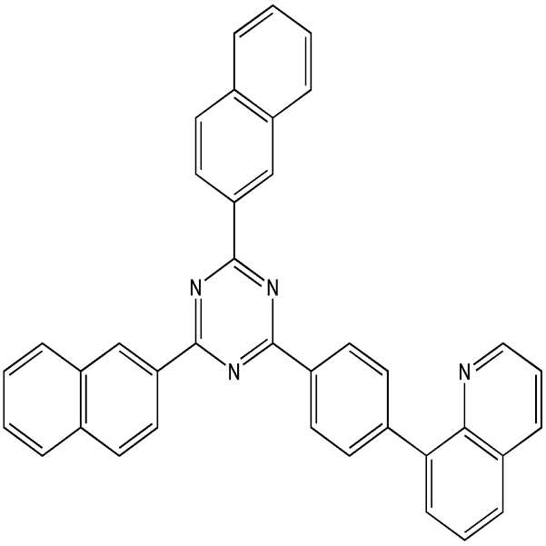
상기 화학식 1로 표현되는 화합물은 구체적으로 하기 화학식 2로 표시되는 화합물, 하기 화학식 3으로 표시되는 화합물 및 이들의 조합에서 선택되는 하나를 포함할 수 있다.The compound represented by
[화학식 2] (2)

[화학식 3](3)
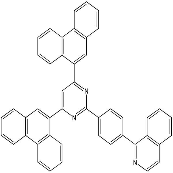
상기 화학식 1로 표현되는 화합물은 R1, R2 및 R3 중 적어도 하나가 헤테로아릴기인 경우, 상기 헤테로아릴기의 헤테로 원자와 L1, L2 및 L3가 직접 연결되지 않을 수 있다. In the compound represented by
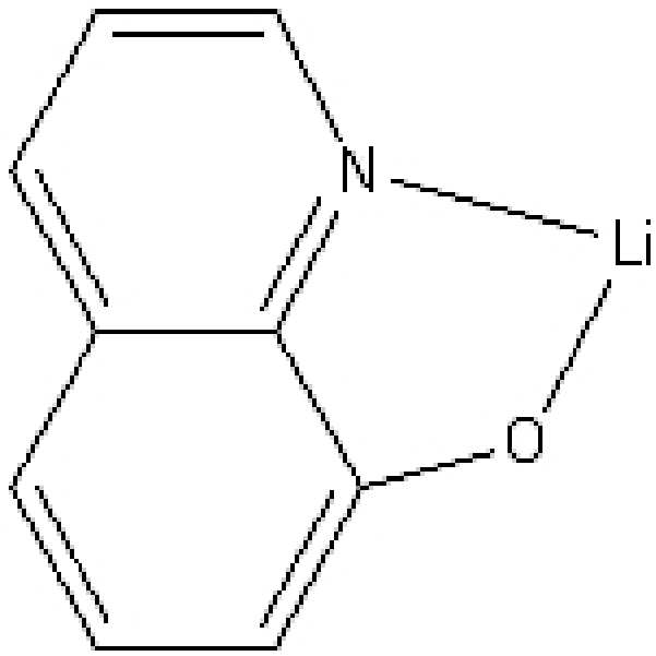
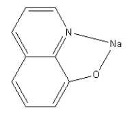
상기 알칼리 금속의 유기 착체는 예를 들면, 알칼리금속의 옥사이드, 플루오라이드, 퀴놀레이트 또는 아세토아세테이트 화합물일 수 있다. 보다 더 구체적으로, 상기 알칼리 금속의 유기 착체는 LiF, NaF, NaCl, CsF, Li2O 리튬퀴놀레이트, 나트륨퀴놀레이트 및 이들의 조합에서 선택되는 하나를 포함할 수 있다. The organic complex of the alkali metal may be, for example, an oxide, fluoride, quinolate or acetoacetate compound of the alkali metal. Even more specifically, the organic complex of the alkali metal may include one selected from LiF, NaF, NaCl, CsF, Li 2 O lithium quinolate, sodium quinolate and combinations thereof.
상기 알칼리 금속의 유기 착체는 예를 들면, 하기 화학식 4로 표시되는 리튬퀴놀레이트 화합물, 하기 화학식 5로 표시되는 리튬퀴놀레이트 화합물 및 이들의 조합에서 선택되는 하나를 포함할 수 있다.The organic complex of the alkali metal may include, for example, a lithium quinolate compound represented by
[화학식 4][Chemical Formula 4]

[화학식 5][Chemical Formula 5]

상기 유기막(140)은 발광층을 더 포함할 수 있다. 발광층은 적색, 녹색, 청색의 삼원색 등 기본색(primary color) 중 어느 하나의 빛을 고유하게 내는 유기 물질 또는 유기 물질과 무기 물질의 혼합물로 만들어지며, 예컨대 폴리플루오렌(polyfluorene) 유도체, (폴리)파라페닐렌비닐렌((poly)paraphenylenevinylene) 유도체, 폴리페닐렌(polyphenylene) 유도체, 폴리플루오렌(polyfluorene) 유도체, 폴리비닐카바졸(polyvinylcarbazole), 폴리티오펜(polythiophene) 유도체 또는 이들의 고분자 재료에 페릴렌(perylene)계 색소, 쿠마린(cumarine)계 색소, 로더민계 색소, 루브렌(rubrene), 페릴렌(perylene), 9,10-디페닐안트라센(9,10-diphenylanthracene), 테트라페닐부타디엔(tetraphenylbutadiene), 나일 레드(Nile red), 쿠마린(coumarin), 퀴나크리돈(quinacridone) 등을 도핑한 화합물이 포함될 수 있다. 유기 발광 장치는 발광층에서 내는 기본색 색광의 공간적인 합으로 원하는 영상을 표시한다.The
상기 유기막(140)은 부대층을 더 포함할 수 있다. 부대층은 상술한 전자 수송층 외에 정공 수송층(hole transport layer), 전자 주입층(electron injection layer) 및 정공 주입층(hole injection layer) 등이 있으며, 이 중에서 선택된 적어도 하나의 층을 포함할 수 있다.The
상기 유기 발광 장치는 저효율 및 장수명의 특성을 구현할 수 있는 것으로서, 전면 발광, 배면 발광, 양면 발광 등 다양한 적용이 가능하고, 특정 구현예에 한정되지 않는다. The organic light emitting device may implement characteristics of low efficiency and long life, and various applications such as top emission, bottom emission, and double emission may be performed, and the present invention is not limited to a specific embodiment.
도 2는 본 발명의 다른 구현예에 따른 유기 발광 장치의 단면도이다.2 is a cross-sectional view of an organic light emitting device according to another embodiment of the present invention.
도 2를 참고하면, 유기 발광 장치(200)는 기판(210) 상에, 제1 전극(220), 제2 전극(260) 및 상기 제1 전극(220)과 제2 전극(260) 사이의 유기 발광층(240)이 배치된다. 상기 제1 전극(220)과 상기 유기 발광층(240) 사이에 하부 보조층(230)이 개재될 수 있다. 상기 유기 발광층(240)과 상기 제2 전극(260) 사이에 상부 보조층(250)이 게재될 수 있다.Referring to FIG. 2, the organic
기판(210), 제1 전극(220) 및 제2 전극(260)은 도 1에서 설명한 바와 같다.The
하부 보조층(230), 유기 발광층(240) 및 상부 보조층(250)은 도 1에서의 유기막(140)을 형성한다.The lower
상기 하부 보조층(230) 및 상기 상부 보조층(250) 중 하나는 정공 주입층 및/또는 정공 수송층을 포함하고, 다른 하나는 전자 수송층 및/또는 전자 주입층을 포함할 수 있다. 예를 들어, 상기 제1 전극(220)이 애노드이고 상기 제2 전극(250)이 캐소드인 경우, 상기 하부 보조층(230)은 정공 주입층 및/또는 정공 수송층을 포함하고 상기 상부 보조층(250)은 전자 주입층 및/또는 전자 수송층을 포함할 수 있다. 이와 달리, 정공 주입층 및/또는 정공 수송층을 포함하는 경우의 하부 보조층(230) 또는 상부 보조층(250)은 생략될 수 있다.One of the lower
유기 발광층(240)은 도 1에서 발광층에 관하여 설명한 바와 같다.The
상기 전자 수송층은 도 1에서 설명한 바와 같다.
The electron transport layer is as described with reference to FIG. 1.
이하 실시예를 통해서 본 발명을 보다 상세하게 설명한다. 다만 하기의 실시예는 단지 설명의 목적을 위한 것이며 본 발명의 범위를 제한하는 것은 아니다.
The present invention will be described in more detail with reference to the following Examples. The following examples are for illustrative purposes only and are not intended to limit the scope of the invention.
유기 발광 장치의 제작Fabrication of Organic Light Emitting Device
실시예Example 1 One
유리 기판 위에 ITO(애노드 전극)를 적층하고 패터닝한 후 정공주입층으로 하기 화학식 a로 표시되는 화합물을 증착하고, 그 위에 정공수송층으로 화학식 b로 표시되는 화합물을 증착한 다음, 그 위에 발광층을 형성하고, 다시 그 위에 다시 전자 수송층으로 하기 화학식 2로 표시되는 화합물 및 리튬퀴놀레이트(Liq)를 1:1 중량비로 공증착하였다. 이어서 그 위에 MgAg를 증착하여 캐소드 전극을 형성하였다.After depositing and patterning ITO (anode electrode) on the glass substrate, the compound represented by Chemical Formula a is deposited as a hole injection layer, and the compound represented by Chemical Formula b is deposited on the hole transport layer, and then a light emitting layer is formed thereon. Then, the compound represented by the following
[화학식 2](2)
[화학식 a](A)

[화학식 b][Formula b]

실시예Example 2 2
전자 수송층으로 화학식 2로 표시되는 화합물 대신 하기 화학식 3으로 표시되는 화합물을 사용하여 화학식 3으로 표시되는 화합물 및 리튬퀴놀레이트(Liq)를 1:1 중량비로 공증착한 것을 제외하고, 실시예 1과 동일한 방법으로 유기 발광 장치를 제작하였다.Except for co-depositing the compound represented by the formula (3) and lithium quinolate (Liq) in a 1: 1 weight ratio by using a compound represented by the following formula (3) instead of the compound represented by the formula (2) as the electron transport layer An organic light emitting device was manufactured by the method.
[화학식 3](3)

비교예Comparative Example 1 One
전자 수송층으로 화학식 2로 표시되는 화합물 대신 하기 화학식 11로 표시되는 화합물을 사용하여 화학식 11으로 표시되는 화합물 및 리튬퀴놀레이트(LiQ)를 1:1 중량비로 공증착한 것을 제외하고, 실시예 1과 동일한 방법으로 유기 발광 장치를 제작하였다.Except for co-depositing the compound represented by the formula (11) and lithium quinolate (LiQ) in a 1: 1 weight ratio using a compound represented by the following formula (11) instead of the compound represented by the formula (2) as the electron transport layer, An organic light emitting device was manufactured by the method.
[화학식 11][Formula 11]
평가 1
상기 실시예들 및 비교예 따른 장치들의 구동 전압, 효율, CIE 색좌표 및 최대 발광 파장을 측정하였다. 측정 결과는 하기 표 1과 같다.The driving voltage, efficiency, CIE color coordinate, and maximum emission wavelength of the devices according to the above examples and comparative examples were measured. The measurement results are shown in Table 1 below.
(V)Driving voltage
(V)
(mA/cm2)Current density
(mA / cm 2 )
(cd/A)Current efficiency
(cd / A)
도 3은 실시예 1 및 비교예 1에 대하여 전압에 따른 전류밀도를 측정하여 나타낸 그래프이고, 도 4는 수명 특성을 평가하기 위하여 실시예 1 및 비교예 1에 대하여 시간에 따른 휘도를 측정하여 나타낸 그래프이다. FIG. 3 is a graph illustrating measurement of current density according to voltage with respect to Example 1 and Comparative Example 1, and FIG. 4 is a graph illustrating measurement of luminance over time for Example 1 and Comparative Example 1 to evaluate life characteristics. It is a graph.
도 3 및 도 4를 참고하면, 실시예 1에 따른 유기 발광 장치는 비교예 1에 따른 유기 발광 장치와 비교하여 낮은 구동 전압, 높은 전류 특성 및 개선된 색 특성을 나타냄을 알 수 있고, 이로부터 효율 및 수명 특성을 개선할 수 있음을 확인할 수 있다.
3 and 4, it can be seen that the organic light emitting device according to Example 1 exhibits a lower driving voltage, a higher current characteristic, and an improved color characteristic as compared to the organic light emitting device according to Comparative Example 1. It can be seen that the efficiency and life characteristics can be improved.
본 발명을 앞서 기재한 바에 따라 바람직한 실시예를 통해 설명하였지만, 본 발명은 이에 한정되지 않으며 다음에 기재하는 특허청구범위의 개념과 범위를 벗어나지 않는 한, 다양한 수정 및 변형이 가능하다는 것을 본 발명이 속하는 기술 분야에 종사하는 자들은 쉽게 이해할 것이다.
Although the present invention has been described through the preferred embodiments as described above, the present invention is not limited thereto and various modifications and variations are possible without departing from the spirit and scope of the claims set out below. Those in the technical field to which they belong will easily understand.
100, 200: 유기 발광 장치
110, 210: 기판 120, 220: 제1 전극
140: 유기막 141: 전자 수송층
160, 260: 제2 전극
230: 하부 보조층 250: 상부 보조층
240: 유기 발광층100, 200: organic light emitting device
110 and 210:
140: organic film 141: electron transport layer
160, 260: second electrode
230: lower auxiliary layer 250: upper auxiliary layer
240: organic light emitting layer
Claims (10)
상기 제1 전극과 마주하는 제2 전극, 및
상기 제1 전극과 상기 제2 전극 사이에 위치하는 유기막을 포함하고,
상기 유기막은 전자 수송층을 포함하고,
상기 전자 수송층은 하기의 화학식 1로 표현되는 화합물 및 알칼리 금속의 유기 착체를 포함하는 유기 발광 장치:
[화학식 1]

상기 식에서,
X는 탄소 또는 질소이고,
L1, L2 및 L3은, 각각 독립적으로, 단일결합, 또는 치환 또는 비치환된 C5 내지 C30 아릴렌기이고,
R1, R2 및 R3은, 각각 독립적으로, 치환 또는 비치환된 C5 내지 C30 아릴기, 치환 또는 비치환된 C2 내지 C30 헤테로아릴기이다.
The first electrode,
A second electrode facing the first electrode, and
An organic film positioned between the first electrode and the second electrode,
The organic layer includes an electron transport layer,
The electron transport layer includes an organic light emitting device including an organic complex of a compound represented by the following Chemical Formula 1 and an alkali metal:
[Chemical Formula 1]
In this formula,
X is carbon or nitrogen,
L 1 , L 2 and L 3 are each independently a single bond or a substituted or unsubstituted C5 to C30 arylene group,
R 1 , R 2 and R 3 are each independently a substituted or unsubstituted C5 to C30 aryl group, or a substituted or unsubstituted C2 to C30 heteroaryl group.
상기 전자 수송층은 상기 화학식 1로 표현되는 화합물 및 상기 알칼리 금속의 유기 착체를 8:2 내지 2:8 중량비로 포함하는 것인 유기 발광 장치.
The method of claim 1,
The electron transport layer includes an organic complex of the compound represented by Formula 1 and the alkali metal in a weight ratio of 8: 2 to 2: 8.
상기 전자 수송층은 단일층 또는 복수층인 유기 발광 장치.
The method of claim 1,
The electron transport layer is an organic light emitting device of a single layer or a plurality of layers.
상기 전자 수송층이 복수층인 경우, 상기 전자 수송층은 상기 화학식 1로 표현되는 화합물 및 상기 알칼리 금속의 유기 착체를 포함하는 하나의 층을 포함하고, 상기 화학식 1로 표현되는 화합물, 알칼리 금속의 유기 착체 및 이들의 조합에서 선택되는 하나를 포함하는 적어도 하나의 층을 더 포함하는 것인 유기 발광 장치.
The method of claim 3,
When the electron transport layer is a plurality of layers, the electron transport layer comprises one layer comprising a compound represented by the formula (1) and an organic complex of the alkali metal, an organic complex of a compound represented by the formula (1), alkali metal And at least one layer comprising one selected from a combination thereof.
상기 화학식 1로 표현되는 화합물은 하기 화학식 2로 표시되는 화합물, 하기 화학식 3으로 표시되는 화합물 및 이들의 조합에서 선택되는 하나를 포함하는 유기 발광 장치.
[화학식 2]

[화학식 3]

The method of claim 1,
The compound represented by Formula 1 is an organic light emitting device comprising one selected from a compound represented by the following formula (2), a compound represented by the following formula (3), and a combination thereof.
(2)
(3)
상기 화학식 1로 표현되는 화합물은 R1, R2 및 R3 중 적어도 하나가 헤테로아릴기인 경우, 상기 헤테로아릴기의 헤테로 원자와 L1, L2 및 L3가 직접 연결되지 않은 것인 유기 발광 장치.
The method of claim 1,
The compound represented by Chemical Formula 1 is an organic light-emitting that at least one of R 1 , R 2 and R 3 is a heteroaryl group, the hetero atom of the heteroaryl group and L 1 , L 2 and L 3 is not directly connected Device.
상기 알칼리 금속의 유기 착체는 알칼리금속의 옥사이드, 플루오라이드, 퀴놀레이트 또는 아세토아세테이트 화합물인 유기 발광 장치.
The method of claim 1,
The organic complex of the alkali metal is an organic light emitting device of the oxide, fluoride, quinolate or acetoacetate compound of the alkali metal.
상기 알칼리 금속의 유기 착체는 LiF, NaF, NaCl, CsF, Li2O, 리튬퀴놀레이트, 나트륨퀴놀레이트 및 이들의 조합에서 선택되는 하나를 포함하는 유기 발광 장치.
The method of claim 1,
The organic complex of the alkali metal is an organic light emitting device comprising one selected from LiF, NaF, NaCl, CsF, Li 2 O, lithium quinolate, sodium quinolate and combinations thereof.
상기 화학식 1로 표현되는 화합물은 하기 화학식 2로 표시되는 화합물, 하기 화학식 3으로 표시되는 화합물 및 이들의 조합에서 선택되는 하나를 포함하고,
상기 알칼리 금속의 유기 착체는 하기 화학식 4로 표시되는 리튬퀴놀레이트 화합물, 하기 화학식 5로 표시되는 리튬퀴놀레이트 화합물 및 이들의 조합에서 선택되는 하나를 포함하는 유기 발광 장치.
[화학식 2]

[화학식 3]

[화학식 4]

[화학식 5]

The method of claim 1,
The compound represented by Chemical Formula 1 includes a compound represented by Chemical Formula 2, a compound represented by Chemical Formula 3, and a combination thereof,
The organic complex of the alkali metal is an organic light emitting device comprising one selected from a lithium quinolate compound represented by the following formula (4), a lithium quinolate compound represented by the following formula (5), and a combination thereof.
(2)
(3)
[Chemical Formula 4]
[Chemical Formula 5]
상기 유기막은 정공주입층, 정공수송층, 전자저지층, 발광층, 정공저지층, 전자 수송층 및 전자주입층으로 이루어진 군으로부터 선택된 적어도 하나의 층을 더 포함하는 것을 특징으로 하는 유기 발광 소자.The method of claim 1,
The organic layer further comprises at least one layer selected from the group consisting of a hole injection layer, a hole transport layer, an electron blocking layer, a light emitting layer, a hole blocking layer, an electron transport layer and an electron injection layer.
Priority Applications (2)
| Application Number | Priority Date | Filing Date | Title |
|---|---|---|---|
| KR1020120075267A KR20140008126A (en) | 2012-07-10 | 2012-07-10 | Organic light emitting device |
| US13/937,141 US20140014927A1 (en) | 2012-07-10 | 2013-07-08 | Organic light emitting device |
Applications Claiming Priority (1)
| Application Number | Priority Date | Filing Date | Title |
|---|---|---|---|
| KR1020120075267A KR20140008126A (en) | 2012-07-10 | 2012-07-10 | Organic light emitting device |
Publications (1)
| Publication Number | Publication Date |
|---|---|
| KR20140008126A true KR20140008126A (en) | 2014-01-21 |
Family
ID=49913201
Family Applications (1)
| Application Number | Title | Priority Date | Filing Date |
|---|---|---|---|
| KR1020120075267A Ceased KR20140008126A (en) | 2012-07-10 | 2012-07-10 | Organic light emitting device |
Country Status (2)
| Country | Link |
|---|---|
| US (1) | US20140014927A1 (en) |
| KR (1) | KR20140008126A (en) |
Cited By (8)
| Publication number | Priority date | Publication date | Assignee | Title |
|---|---|---|---|---|
| KR101537499B1 (en) * | 2014-04-04 | 2015-07-16 | 주식회사 엘지화학 | Organic light emitting diode |
| US10177334B2 (en) | 2015-03-16 | 2019-01-08 | Samsung Display Co., Ltd. | Organic light emitting device and display device having the same |
| US10230051B2 (en) | 2014-02-20 | 2019-03-12 | Samsung Display Co., Ltd. | Organic light-emitting device |
| CN110024155A (en) * | 2017-05-15 | 2019-07-16 | 株式会社Lg化学 | Organic light emitting device |
| US10381572B2 (en) | 2014-04-04 | 2019-08-13 | Lg Chem, Ltd. | Heterocyclic compound and organic light-emitting element comprising same |
| US10964892B2 (en) | 2014-04-04 | 2021-03-30 | Lg Chem, Ltd. | Heterocyclic compound and organic light-emitting device comprising same |
| CN113195468A (en) * | 2018-12-21 | 2021-07-30 | 诺瓦尔德股份有限公司 | Compound, and organic semiconductor layer, organic electronic device and display device comprising the same |
| US11271167B2 (en) | 2014-04-04 | 2022-03-08 | Lg Chem, Ltd. | Organic light-emitting device |
Families Citing this family (86)
| Publication number | Priority date | Publication date | Assignee | Title |
|---|---|---|---|---|
| KR102046157B1 (en) * | 2012-12-21 | 2019-12-03 | 삼성디스플레이 주식회사 | Organic light emitting diode display and manufacturing method thereof |
| KR102343147B1 (en) * | 2014-06-12 | 2021-12-29 | 삼성디스플레이 주식회사 | Organic light- emitting device |
| US10038147B2 (en) * | 2014-06-12 | 2018-07-31 | Samsung Display Co., Ltd. | Organic light-emitting device |
| EP3002796A1 (en) * | 2014-10-01 | 2016-04-06 | Novaled GmbH | Organic light-emitting diode including an electron transport layer comprising a three component blend of a matrix compound and two lithium compounds |
| KR102376968B1 (en) * | 2014-11-17 | 2022-03-22 | 삼성디스플레이 주식회사 | Organic light-emitting devices |
| US9929361B2 (en) | 2015-02-16 | 2018-03-27 | Universal Display Corporation | Organic electroluminescent materials and devices |
| US11056657B2 (en) | 2015-02-27 | 2021-07-06 | University Display Corporation | Organic electroluminescent materials and devices |
| US9859510B2 (en) | 2015-05-15 | 2018-01-02 | Universal Display Corporation | Organic electroluminescent materials and devices |
| US10418568B2 (en) | 2015-06-01 | 2019-09-17 | Universal Display Corporation | Organic electroluminescent materials and devices |
| US11127905B2 (en) | 2015-07-29 | 2021-09-21 | Universal Display Corporation | Organic electroluminescent materials and devices |
| US10672996B2 (en) | 2015-09-03 | 2020-06-02 | Universal Display Corporation | Organic electroluminescent materials and devices |
| US20170229663A1 (en) | 2016-02-09 | 2017-08-10 | Universal Display Corporation | Organic electroluminescent materials and devices |
| US10236456B2 (en) | 2016-04-11 | 2019-03-19 | Universal Display Corporation | Organic electroluminescent materials and devices |
| US10672997B2 (en) | 2016-06-20 | 2020-06-02 | Universal Display Corporation | Organic electroluminescent materials and devices |
| US10862054B2 (en) | 2016-06-20 | 2020-12-08 | Universal Display Corporation | Organic electroluminescent materials and devices |
| US11482683B2 (en) | 2016-06-20 | 2022-10-25 | Universal Display Corporation | Organic electroluminescent materials and devices |
| US10608186B2 (en) | 2016-09-14 | 2020-03-31 | Universal Display Corporation | Organic electroluminescent materials and devices |
| US10680187B2 (en) | 2016-09-23 | 2020-06-09 | Universal Display Corporation | Organic electroluminescent materials and devices |
| US11196010B2 (en) | 2016-10-03 | 2021-12-07 | Universal Display Corporation | Organic electroluminescent materials and devices |
| US11011709B2 (en) | 2016-10-07 | 2021-05-18 | Universal Display Corporation | Organic electroluminescent materials and devices |
| US12317745B2 (en) | 2016-11-09 | 2025-05-27 | Universal Display Corporation | Organic electroluminescent materials and devices |
| US10680188B2 (en) | 2016-11-11 | 2020-06-09 | Universal Display Corporation | Organic electroluminescent materials and devices |
| US11780865B2 (en) | 2017-01-09 | 2023-10-10 | Universal Display Corporation | Organic electroluminescent materials and devices |
| KR20190111948A (en) * | 2017-01-30 | 2019-10-02 | 이데미쓰 고산 가부시키가이샤 | Organic electroluminescent device and electronic device |
| US10844085B2 (en) | 2017-03-29 | 2020-11-24 | Universal Display Corporation | Organic electroluminescent materials and devices |
| US10944060B2 (en) | 2017-05-11 | 2021-03-09 | Universal Display Corporation | Organic electroluminescent materials and devices |
| KR102032955B1 (en) * | 2017-06-07 | 2019-10-16 | 주식회사 엘지화학 | Novel hetero-cyclic compound and organic light emitting device comprising the same |
| US12098157B2 (en) | 2017-06-23 | 2024-09-24 | Universal Display Corporation | Organic electroluminescent materials and devices |
| US11228010B2 (en) | 2017-07-26 | 2022-01-18 | Universal Display Corporation | Organic electroluminescent materials and devices |
| US11744142B2 (en) | 2017-08-10 | 2023-08-29 | Universal Display Corporation | Organic electroluminescent materials and devices |
| KR102401011B1 (en) * | 2017-08-16 | 2022-05-24 | 삼성디스플레이 주식회사 | Organic light emitting device and apparatus comprising the same |
| US12180230B2 (en) | 2017-11-28 | 2024-12-31 | University Of Southern California | Carbene compounds and organic electroluminescent devices |
| EP3492480B1 (en) | 2017-11-29 | 2021-10-20 | Universal Display Corporation | Organic electroluminescent materials and devices |
| US11937503B2 (en) | 2017-11-30 | 2024-03-19 | Universal Display Corporation | Organic electroluminescent materials and devices |
| US11542289B2 (en) | 2018-01-26 | 2023-01-03 | Universal Display Corporation | Organic electroluminescent materials and devices |
| US11165028B2 (en) | 2018-03-12 | 2021-11-02 | Universal Display Corporation | Organic electroluminescent materials and devices |
| US12453279B2 (en) | 2018-08-22 | 2025-10-21 | Universal Display Corporation | Organic electroluminescent materials and devices |
| US11737349B2 (en) | 2018-12-12 | 2023-08-22 | Universal Display Corporation | Organic electroluminescent materials and devices |
| US11780829B2 (en) | 2019-01-30 | 2023-10-10 | The University Of Southern California | Organic electroluminescent materials and devices |
| US12477890B2 (en) | 2019-02-01 | 2025-11-18 | Universal Display Corporation | Organic electroluminescent materials and devices |
| JP2020158491A (en) | 2019-03-26 | 2020-10-01 | ユニバーサル ディスプレイ コーポレイション | Organic electroluminescent materials and devices |
| TW202513513A (en) * | 2019-06-14 | 2025-04-01 | 日商半導體能源研究所股份有限公司 | Light-emitting device, light-emitting apparatus, electronic device, and lighting device |
| US12281128B2 (en) | 2019-07-30 | 2025-04-22 | Universal Display Corporation | Organic electroluminescent materials and devices |
| US12139501B2 (en) | 2019-08-16 | 2024-11-12 | Universal Display Corporation | Organic electroluminescent materials and devices |
| US20210135130A1 (en) | 2019-11-04 | 2021-05-06 | Universal Display Corporation | Organic electroluminescent materials and devices |
| US20230099759A1 (en) * | 2019-12-23 | 2023-03-30 | Idemitsu Kosan Co.,Ltd. | Polycyclic compound, material for an organic electroluminescence device and an organic electroluminescence device comprising the polycyclic compound |
| US12538698B2 (en) | 2020-01-06 | 2026-01-27 | Universal Display Corporation | Organic electroluminescent materials and devices |
| US12426495B2 (en) | 2020-01-28 | 2025-09-23 | Universal Display Corporation | Organic electroluminescent materials and devices |
| EP3937268B1 (en) | 2020-07-10 | 2025-05-07 | Universal Display Corporation | Plasmonic oleds and vertical dipole emitters |
| US12187748B2 (en) | 2020-11-02 | 2025-01-07 | Universal Display Corporation | Organic electroluminescent materials and devices |
| US20220158096A1 (en) | 2020-11-16 | 2022-05-19 | Universal Display Corporation | Organic electroluminescent materials and devices |
| US12325717B2 (en) | 2020-11-24 | 2025-06-10 | Universal Display Corporation | Organic electroluminescent materials and devices |
| US20220165967A1 (en) | 2020-11-24 | 2022-05-26 | Universal Display Corporation | Organic electroluminescent materials and devices |
| US20220271241A1 (en) | 2021-02-03 | 2022-08-25 | Universal Display Corporation | Organic electroluminescent materials and devices |
| EP4060758A3 (en) | 2021-02-26 | 2023-03-29 | Universal Display Corporation | Organic electroluminescent materials and devices |
| EP4059915B1 (en) | 2021-02-26 | 2025-12-24 | Universal Display Corporation | Organic electroluminescent materials and devices |
| US20220298192A1 (en) | 2021-03-05 | 2022-09-22 | Universal Display Corporation | Organic electroluminescent materials and devices |
| US12428599B2 (en) | 2021-03-09 | 2025-09-30 | Universal Display Corporation | Organic electroluminescent materials and devices |
| US20220298190A1 (en) | 2021-03-12 | 2022-09-22 | Universal Display Corporation | Organic electroluminescent materials and devices |
| US12421262B2 (en) | 2021-03-15 | 2025-09-23 | Universal Display Corporation | Organic electroluminescent materials and devices |
| US20220340607A1 (en) | 2021-04-05 | 2022-10-27 | Universal Display Corporation | Organic electroluminescent materials and devices |
| US12480042B2 (en) | 2021-04-09 | 2025-11-25 | Universal Display Corporation | Organic electroluminescent materials and devices |
| EP4075531A1 (en) | 2021-04-13 | 2022-10-19 | Universal Display Corporation | Plasmonic oleds and vertical dipole emitters |
| US20220352478A1 (en) | 2021-04-14 | 2022-11-03 | Universal Display Corporation | Organic eletroluminescent materials and devices |
| US20220407020A1 (en) | 2021-04-23 | 2022-12-22 | Universal Display Corporation | Organic electroluminescent materials and devices |
| US20230006149A1 (en) | 2021-04-23 | 2023-01-05 | Universal Display Corporation | Organic electroluminescent materials and devices |
| US20230133787A1 (en) | 2021-06-08 | 2023-05-04 | University Of Southern California | Molecular Alignment of Homoleptic Iridium Phosphors |
| JP7643957B2 (en) * | 2021-06-30 | 2025-03-11 | 出光興産株式会社 | Compound, material for organic electroluminescence device, organic electroluminescence device, and electronic device |
| EP4151699A1 (en) | 2021-09-17 | 2023-03-22 | Universal Display Corporation | Organic electroluminescent materials and devices |
| US12473318B2 (en) | 2021-10-08 | 2025-11-18 | Universal Display Corporation | Organic electroluminescent materials and devices |
| US12509628B2 (en) | 2021-12-16 | 2025-12-30 | Universal Display Corporation | Organic electroluminescent materials and devices |
| EP4231804A3 (en) | 2022-02-16 | 2023-09-20 | Universal Display Corporation | Organic electroluminescent materials and devices |
| US20230292592A1 (en) | 2022-03-09 | 2023-09-14 | Universal Display Corporation | Organic electroluminescent materials and devices |
| US20230337516A1 (en) | 2022-04-18 | 2023-10-19 | Universal Display Corporation | Organic electroluminescent materials and devices |
| US20230389421A1 (en) | 2022-05-24 | 2023-11-30 | Universal Display Corporation | Organic electroluminescent materials and devices |
| EP4293001A1 (en) | 2022-06-08 | 2023-12-20 | Universal Display Corporation | Organic electroluminescent materials and devices |
| US20240016051A1 (en) | 2022-06-28 | 2024-01-11 | Universal Display Corporation | Organic electroluminescent materials and devices |
| US20240107880A1 (en) | 2022-08-17 | 2024-03-28 | Universal Display Corporation | Organic electroluminescent materials and devices |
| US20240180025A1 (en) | 2022-10-27 | 2024-05-30 | Universal Display Corporation | Organic electroluminescent materials and devices |
| US20240188316A1 (en) | 2022-10-27 | 2024-06-06 | Universal Display Corporation | Organic electroluminescent materials and devices |
| US20240188319A1 (en) | 2022-10-27 | 2024-06-06 | Universal Display Corporation | Organic electroluminescent materials and devices |
| US20240196730A1 (en) | 2022-10-27 | 2024-06-13 | Universal Display Corporation | Organic electroluminescent materials and devices |
| US20240188419A1 (en) | 2022-10-27 | 2024-06-06 | Universal Display Corporation | Organic electroluminescent materials and devices |
| US20240247017A1 (en) | 2022-12-14 | 2024-07-25 | Universal Display Corporation | Organic electroluminescent materials and devices |
| US20250204238A1 (en) | 2023-12-15 | 2025-06-19 | Universal Display Corporation | Organic electroluminscent materials and devices |
| US20250204239A1 (en) | 2023-12-15 | 2025-06-19 | Universal Display Corporation | Organic electroluminescent materials and devices |
Family Cites Families (11)
| Publication number | Priority date | Publication date | Assignee | Title |
|---|---|---|---|---|
| JP4505067B2 (en) * | 1998-12-16 | 2010-07-14 | 淳二 城戸 | Organic electroluminescent device |
| KR100730140B1 (en) * | 2005-07-15 | 2007-06-19 | 삼성에스디아이 주식회사 | Triazine Compound and Organic Light-Emitting Device Using the Same |
| KR100795817B1 (en) * | 2007-02-20 | 2008-01-21 | 삼성에스디아이 주식회사 | Organic light emitting device, method for manufacturing same and method for forming organic layer |
| US8476822B2 (en) * | 2007-11-09 | 2013-07-02 | Universal Display Corporation | Saturated color organic light emitting devices |
| KR100918401B1 (en) * | 2007-12-24 | 2009-09-24 | 삼성모바일디스플레이주식회사 | Organic light emitting device |
| KR101288557B1 (en) * | 2008-12-24 | 2013-07-22 | 제일모직주식회사 | Novel compound for organic photoelectric device and organic photoelectric device including the same |
| KR101279121B1 (en) * | 2009-09-29 | 2013-06-26 | 엘지디스플레이 주식회사 | Organic Light Emitting Display Device |
| JP5851683B2 (en) * | 2009-10-14 | 2016-02-03 | 三星ディスプレイ株式會社Samsung Display Co.,Ltd. | ORGANIC LIGHT EMITTING DEVICE AND MANUFACTURING METHOD THEREOF |
| KR101387738B1 (en) * | 2009-12-29 | 2014-04-22 | 제일모직주식회사 | Compound for organic photoelectric device and organic photoelectric device including the same |
| KR101657222B1 (en) * | 2010-05-14 | 2016-09-19 | 삼성디스플레이 주식회사 | Organic light emitting device |
| KR20120010438A (en) * | 2010-07-26 | 2012-02-03 | 삼성모바일디스플레이주식회사 | Organic light emitting device |
-
2012
- 2012-07-10 KR KR1020120075267A patent/KR20140008126A/en not_active Ceased
-
2013
- 2013-07-08 US US13/937,141 patent/US20140014927A1/en not_active Abandoned
Cited By (13)
| Publication number | Priority date | Publication date | Assignee | Title |
|---|---|---|---|---|
| US10230051B2 (en) | 2014-02-20 | 2019-03-12 | Samsung Display Co., Ltd. | Organic light-emitting device |
| US11271167B2 (en) | 2014-04-04 | 2022-03-08 | Lg Chem, Ltd. | Organic light-emitting device |
| US9640766B2 (en) | 2014-04-04 | 2017-05-02 | Lg Chem, Ltd. | Organic light emitting diode |
| WO2015152644A1 (en) * | 2014-04-04 | 2015-10-08 | 주식회사 엘지화학 | Organic light-emitting device |
| US10381572B2 (en) | 2014-04-04 | 2019-08-13 | Lg Chem, Ltd. | Heterocyclic compound and organic light-emitting element comprising same |
| US10964892B2 (en) | 2014-04-04 | 2021-03-30 | Lg Chem, Ltd. | Heterocyclic compound and organic light-emitting device comprising same |
| KR101537499B1 (en) * | 2014-04-04 | 2015-07-16 | 주식회사 엘지화학 | Organic light emitting diode |
| US11342508B2 (en) | 2014-04-04 | 2022-05-24 | Lg Chem, Ltd. | Organic light-emitting device |
| US11362280B2 (en) | 2014-04-04 | 2022-06-14 | Lg Chem, Ltd. | Organic light-emitting device |
| US10177334B2 (en) | 2015-03-16 | 2019-01-08 | Samsung Display Co., Ltd. | Organic light emitting device and display device having the same |
| CN110024155A (en) * | 2017-05-15 | 2019-07-16 | 株式会社Lg化学 | Organic light emitting device |
| CN110024155B (en) * | 2017-05-15 | 2023-07-04 | 株式会社Lg化学 | Organic light emitting device |
| CN113195468A (en) * | 2018-12-21 | 2021-07-30 | 诺瓦尔德股份有限公司 | Compound, and organic semiconductor layer, organic electronic device and display device comprising the same |
Also Published As
| Publication number | Publication date |
|---|---|
| US20140014927A1 (en) | 2014-01-16 |
Similar Documents
| Publication | Publication Date | Title |
|---|---|---|
| KR20140008126A (en) | Organic light emitting device | |
| KR101587307B1 (en) | White phosphorescent organic light emitting devices | |
| JP6246990B2 (en) | Organic light emitting diode device | |
| KR101772662B1 (en) | Organic light emitting diode device | |
| KR101760004B1 (en) | Oled device with stabilized yellow light-emitting layer | |
| KR20170008358A (en) | Organic light-emitting display device | |
| KR20110125861A (en) | Organic light emitting device | |
| KR100838094B1 (en) | Organic EL device and light emitting device using the same | |
| KR20130014103A (en) | Organic light emitting diode display | |
| KR102081113B1 (en) | Organic light emitting display | |
| JP2009093981A (en) | Organic electroluminescence device and electronic device | |
| JP4916137B2 (en) | Organic electroluminescence device | |
| KR101481822B1 (en) | Organic light emitting diode and organic electro-luminesence display device | |
| JP5900847B2 (en) | Organic electroluminescence device | |
| KR102020484B1 (en) | Organic light emitting diode device | |
| JP2011146598A (en) | Organic electroluminescent light-emitting device | |
| CN105895819A (en) | OLED device, preparation method therefor, and OLED display panel | |
| KR20120128483A (en) | Organic light emitting diode device | |
| JP5791129B2 (en) | ORGANIC ELECTROLUMINESCENT ELEMENT AND ORGANIC ELECTROLUMINESCENT LIGHTING DEVICE | |
| KR20150052449A (en) | Organic light emitting device | |
| KR101936035B1 (en) | Organic light emitting diode | |
| KR102081122B1 (en) | Organic light emitting display | |
| Yang et al. | Influence of the hole transport layer on spectral stability in the white phosphorescent organic light emitting diode with non-doped structure | |
| JP2006108190A (en) | Electroluminescence element | |
| KR100760901B1 (en) | The White Organic Light Emitting Device |
Legal Events
| Date | Code | Title | Description |
|---|---|---|---|
| PA0109 | Patent application |
St.27 status event code: A-0-1-A10-A12-nap-PA0109 |
|
| PG1501 | Laying open of application |
St.27 status event code: A-1-1-Q10-Q12-nap-PG1501 |
|
| R18-X000 | Changes to party contact information recorded |
St.27 status event code: A-3-3-R10-R18-oth-X000 |
|
| E14-X000 | Pre-grant third party observation filed |
St.27 status event code: A-2-3-E10-E14-opp-X000 |
|
| E14-X000 | Pre-grant third party observation filed |
St.27 status event code: A-2-3-E10-E14-opp-X000 |
|
| R18-X000 | Changes to party contact information recorded |
St.27 status event code: A-3-3-R10-R18-oth-X000 |
|
| A201 | Request for examination | ||
| PA0201 | Request for examination |
St.27 status event code: A-1-2-D10-D11-exm-PA0201 |
|
| E902 | Notification of reason for refusal | ||
| PE0902 | Notice of grounds for rejection |
St.27 status event code: A-1-2-D10-D21-exm-PE0902 |
|
| R18-X000 | Changes to party contact information recorded |
St.27 status event code: A-3-3-R10-R18-oth-X000 |
|
| E601 | Decision to refuse application | ||
| PE0601 | Decision on rejection of patent |
St.27 status event code: N-2-6-B10-B15-exm-PE0601 |
|
| R18-X000 | Changes to party contact information recorded |
St.27 status event code: A-3-3-R10-R18-oth-X000 |
|
| R18-X000 | Changes to party contact information recorded |
St.27 status event code: A-3-3-R10-R18-oth-X000 |
|
| P22-X000 | Classification modified |
St.27 status event code: A-2-2-P10-P22-nap-X000 |
|
| P22-X000 | Classification modified |
St.27 status event code: A-2-2-P10-P22-nap-X000 |
|
| P22-X000 | Classification modified |
St.27 status event code: A-2-2-P10-P22-nap-X000 |