KR20130069561A - Wireless energy transfer converter - Google Patents
Wireless energy transfer converter Download PDFInfo
- Publication number
- KR20130069561A KR20130069561A KR1020127026425A KR20127026425A KR20130069561A KR 20130069561 A KR20130069561 A KR 20130069561A KR 1020127026425 A KR1020127026425 A KR 1020127026425A KR 20127026425 A KR20127026425 A KR 20127026425A KR 20130069561 A KR20130069561 A KR 20130069561A
- Authority
- KR
- South Korea
- Prior art keywords
- resonator
- source
- power
- parameters
- wireless power
- Prior art date
- Legal status (The legal status is an assumption and is not a legal conclusion. Google has not performed a legal analysis and makes no representation as to the accuracy of the status listed.)
- Withdrawn
Links
Images


Classifications
-
- H—ELECTRICITY
- H02—GENERATION; CONVERSION OR DISTRIBUTION OF ELECTRIC POWER
- H02J—CIRCUIT ARRANGEMENTS OR SYSTEMS FOR SUPPLYING OR DISTRIBUTING ELECTRIC POWER; SYSTEMS FOR STORING ELECTRIC ENERGY
- H02J50/00—Circuit arrangements or systems for wireless supply or distribution of electric power
- H02J50/10—Circuit arrangements or systems for wireless supply or distribution of electric power using inductive coupling
- H02J50/12—Circuit arrangements or systems for wireless supply or distribution of electric power using inductive coupling of the resonant type
-
- H—ELECTRICITY
- H04—ELECTRIC COMMUNICATION TECHNIQUE
- H04B—TRANSMISSION
- H04B5/00—Near-field transmission systems, e.g. inductive or capacitive transmission systems
- H04B5/20—Near-field transmission systems, e.g. inductive or capacitive transmission systems characterised by the transmission technique; characterised by the transmission medium
- H04B5/24—Inductive coupling
- H04B5/26—Inductive coupling using coils
- H04B5/263—Multiple coils at either side
-
- B—PERFORMING OPERATIONS; TRANSPORTING
- B60—VEHICLES IN GENERAL
- B60L—PROPULSION OF ELECTRICALLY-PROPELLED VEHICLES; SUPPLYING ELECTRIC POWER FOR AUXILIARY EQUIPMENT OF ELECTRICALLY-PROPELLED VEHICLES; ELECTRODYNAMIC BRAKE SYSTEMS FOR VEHICLES IN GENERAL; MAGNETIC SUSPENSION OR LEVITATION FOR VEHICLES; MONITORING OPERATING VARIABLES OF ELECTRICALLY-PROPELLED VEHICLES; ELECTRIC SAFETY DEVICES FOR ELECTRICALLY-PROPELLED VEHICLES
- B60L53/00—Methods of charging batteries, specially adapted for electric vehicles; Charging stations or on-board charging equipment therefor; Exchange of energy storage elements in electric vehicles
- B60L53/10—Methods of charging batteries, specially adapted for electric vehicles; Charging stations or on-board charging equipment therefor; Exchange of energy storage elements in electric vehicles characterised by the energy transfer between the charging station and the vehicle
- B60L53/12—Inductive energy transfer
- B60L53/126—Methods for pairing a vehicle and a charging station, e.g. establishing a one-to-one relation between a wireless power transmitter and a wireless power receiver
-
- B—PERFORMING OPERATIONS; TRANSPORTING
- B60—VEHICLES IN GENERAL
- B60L—PROPULSION OF ELECTRICALLY-PROPELLED VEHICLES; SUPPLYING ELECTRIC POWER FOR AUXILIARY EQUIPMENT OF ELECTRICALLY-PROPELLED VEHICLES; ELECTRODYNAMIC BRAKE SYSTEMS FOR VEHICLES IN GENERAL; MAGNETIC SUSPENSION OR LEVITATION FOR VEHICLES; MONITORING OPERATING VARIABLES OF ELECTRICALLY-PROPELLED VEHICLES; ELECTRIC SAFETY DEVICES FOR ELECTRICALLY-PROPELLED VEHICLES
- B60L53/00—Methods of charging batteries, specially adapted for electric vehicles; Charging stations or on-board charging equipment therefor; Exchange of energy storage elements in electric vehicles
- B60L53/10—Methods of charging batteries, specially adapted for electric vehicles; Charging stations or on-board charging equipment therefor; Exchange of energy storage elements in electric vehicles characterised by the energy transfer between the charging station and the vehicle
- B60L53/12—Inductive energy transfer
- B60L53/122—Circuits or methods for driving the primary coil, e.g. supplying electric power to the coil
-
- B—PERFORMING OPERATIONS; TRANSPORTING
- B60—VEHICLES IN GENERAL
- B60L—PROPULSION OF ELECTRICALLY-PROPELLED VEHICLES; SUPPLYING ELECTRIC POWER FOR AUXILIARY EQUIPMENT OF ELECTRICALLY-PROPELLED VEHICLES; ELECTRODYNAMIC BRAKE SYSTEMS FOR VEHICLES IN GENERAL; MAGNETIC SUSPENSION OR LEVITATION FOR VEHICLES; MONITORING OPERATING VARIABLES OF ELECTRICALLY-PROPELLED VEHICLES; ELECTRIC SAFETY DEVICES FOR ELECTRICALLY-PROPELLED VEHICLES
- B60L53/00—Methods of charging batteries, specially adapted for electric vehicles; Charging stations or on-board charging equipment therefor; Exchange of energy storage elements in electric vehicles
- B60L53/10—Methods of charging batteries, specially adapted for electric vehicles; Charging stations or on-board charging equipment therefor; Exchange of energy storage elements in electric vehicles characterised by the energy transfer between the charging station and the vehicle
- B60L53/12—Inductive energy transfer
- B60L53/124—Detection or removal of foreign bodies
-
- B—PERFORMING OPERATIONS; TRANSPORTING
- B60—VEHICLES IN GENERAL
- B60L—PROPULSION OF ELECTRICALLY-PROPELLED VEHICLES; SUPPLYING ELECTRIC POWER FOR AUXILIARY EQUIPMENT OF ELECTRICALLY-PROPELLED VEHICLES; ELECTRODYNAMIC BRAKE SYSTEMS FOR VEHICLES IN GENERAL; MAGNETIC SUSPENSION OR LEVITATION FOR VEHICLES; MONITORING OPERATING VARIABLES OF ELECTRICALLY-PROPELLED VEHICLES; ELECTRIC SAFETY DEVICES FOR ELECTRICALLY-PROPELLED VEHICLES
- B60L53/00—Methods of charging batteries, specially adapted for electric vehicles; Charging stations or on-board charging equipment therefor; Exchange of energy storage elements in electric vehicles
- B60L53/50—Charging stations characterised by energy-storage or power-generation means
- B60L53/51—Photovoltaic means
-
- B—PERFORMING OPERATIONS; TRANSPORTING
- B60—VEHICLES IN GENERAL
- B60L—PROPULSION OF ELECTRICALLY-PROPELLED VEHICLES; SUPPLYING ELECTRIC POWER FOR AUXILIARY EQUIPMENT OF ELECTRICALLY-PROPELLED VEHICLES; ELECTRODYNAMIC BRAKE SYSTEMS FOR VEHICLES IN GENERAL; MAGNETIC SUSPENSION OR LEVITATION FOR VEHICLES; MONITORING OPERATING VARIABLES OF ELECTRICALLY-PROPELLED VEHICLES; ELECTRIC SAFETY DEVICES FOR ELECTRICALLY-PROPELLED VEHICLES
- B60L53/00—Methods of charging batteries, specially adapted for electric vehicles; Charging stations or on-board charging equipment therefor; Exchange of energy storage elements in electric vehicles
- B60L53/50—Charging stations characterised by energy-storage or power-generation means
- B60L53/52—Wind-driven generators
-
- B—PERFORMING OPERATIONS; TRANSPORTING
- B60—VEHICLES IN GENERAL
- B60L—PROPULSION OF ELECTRICALLY-PROPELLED VEHICLES; SUPPLYING ELECTRIC POWER FOR AUXILIARY EQUIPMENT OF ELECTRICALLY-PROPELLED VEHICLES; ELECTRODYNAMIC BRAKE SYSTEMS FOR VEHICLES IN GENERAL; MAGNETIC SUSPENSION OR LEVITATION FOR VEHICLES; MONITORING OPERATING VARIABLES OF ELECTRICALLY-PROPELLED VEHICLES; ELECTRIC SAFETY DEVICES FOR ELECTRICALLY-PROPELLED VEHICLES
- B60L53/00—Methods of charging batteries, specially adapted for electric vehicles; Charging stations or on-board charging equipment therefor; Exchange of energy storage elements in electric vehicles
- B60L53/60—Monitoring or controlling charging stations
- B60L53/63—Monitoring or controlling charging stations in response to network capacity
-
- B—PERFORMING OPERATIONS; TRANSPORTING
- B60—VEHICLES IN GENERAL
- B60L—PROPULSION OF ELECTRICALLY-PROPELLED VEHICLES; SUPPLYING ELECTRIC POWER FOR AUXILIARY EQUIPMENT OF ELECTRICALLY-PROPELLED VEHICLES; ELECTRODYNAMIC BRAKE SYSTEMS FOR VEHICLES IN GENERAL; MAGNETIC SUSPENSION OR LEVITATION FOR VEHICLES; MONITORING OPERATING VARIABLES OF ELECTRICALLY-PROPELLED VEHICLES; ELECTRIC SAFETY DEVICES FOR ELECTRICALLY-PROPELLED VEHICLES
- B60L53/00—Methods of charging batteries, specially adapted for electric vehicles; Charging stations or on-board charging equipment therefor; Exchange of energy storage elements in electric vehicles
- B60L53/60—Monitoring or controlling charging stations
- B60L53/64—Optimising energy costs, e.g. responding to electricity rates
-
- B—PERFORMING OPERATIONS; TRANSPORTING
- B60—VEHICLES IN GENERAL
- B60L—PROPULSION OF ELECTRICALLY-PROPELLED VEHICLES; SUPPLYING ELECTRIC POWER FOR AUXILIARY EQUIPMENT OF ELECTRICALLY-PROPELLED VEHICLES; ELECTRODYNAMIC BRAKE SYSTEMS FOR VEHICLES IN GENERAL; MAGNETIC SUSPENSION OR LEVITATION FOR VEHICLES; MONITORING OPERATING VARIABLES OF ELECTRICALLY-PROPELLED VEHICLES; ELECTRIC SAFETY DEVICES FOR ELECTRICALLY-PROPELLED VEHICLES
- B60L53/00—Methods of charging batteries, specially adapted for electric vehicles; Charging stations or on-board charging equipment therefor; Exchange of energy storage elements in electric vehicles
- B60L53/60—Monitoring or controlling charging stations
- B60L53/65—Monitoring or controlling charging stations involving identification of vehicles or their battery types
-
- B—PERFORMING OPERATIONS; TRANSPORTING
- B60—VEHICLES IN GENERAL
- B60L—PROPULSION OF ELECTRICALLY-PROPELLED VEHICLES; SUPPLYING ELECTRIC POWER FOR AUXILIARY EQUIPMENT OF ELECTRICALLY-PROPELLED VEHICLES; ELECTRODYNAMIC BRAKE SYSTEMS FOR VEHICLES IN GENERAL; MAGNETIC SUSPENSION OR LEVITATION FOR VEHICLES; MONITORING OPERATING VARIABLES OF ELECTRICALLY-PROPELLED VEHICLES; ELECTRIC SAFETY DEVICES FOR ELECTRICALLY-PROPELLED VEHICLES
- B60L53/00—Methods of charging batteries, specially adapted for electric vehicles; Charging stations or on-board charging equipment therefor; Exchange of energy storage elements in electric vehicles
- B60L53/60—Monitoring or controlling charging stations
- B60L53/66—Data transfer between charging stations and vehicles
- B60L53/665—Methods related to measuring, billing or payment
-
- B—PERFORMING OPERATIONS; TRANSPORTING
- B60—VEHICLES IN GENERAL
- B60L—PROPULSION OF ELECTRICALLY-PROPELLED VEHICLES; SUPPLYING ELECTRIC POWER FOR AUXILIARY EQUIPMENT OF ELECTRICALLY-PROPELLED VEHICLES; ELECTRODYNAMIC BRAKE SYSTEMS FOR VEHICLES IN GENERAL; MAGNETIC SUSPENSION OR LEVITATION FOR VEHICLES; MONITORING OPERATING VARIABLES OF ELECTRICALLY-PROPELLED VEHICLES; ELECTRIC SAFETY DEVICES FOR ELECTRICALLY-PROPELLED VEHICLES
- B60L55/00—Arrangements for supplying energy stored within a vehicle to a power network, i.e. vehicle-to-grid [V2G] arrangements
-
- H—ELECTRICITY
- H02—GENERATION; CONVERSION OR DISTRIBUTION OF ELECTRIC POWER
- H02J—CIRCUIT ARRANGEMENTS OR SYSTEMS FOR SUPPLYING OR DISTRIBUTING ELECTRIC POWER; SYSTEMS FOR STORING ELECTRIC ENERGY
- H02J50/00—Circuit arrangements or systems for wireless supply or distribution of electric power
- H02J50/40—Circuit arrangements or systems for wireless supply or distribution of electric power using two or more transmitting or receiving devices
-
- H—ELECTRICITY
- H04—ELECTRIC COMMUNICATION TECHNIQUE
- H04B—TRANSMISSION
- H04B5/00—Near-field transmission systems, e.g. inductive or capacitive transmission systems
- H04B5/20—Near-field transmission systems, e.g. inductive or capacitive transmission systems characterised by the transmission technique; characterised by the transmission medium
- H04B5/24—Inductive coupling
- H04B5/26—Inductive coupling using coils
- H04B5/266—One coil at each side, e.g. with primary and secondary coils
-
- H—ELECTRICITY
- H04—ELECTRIC COMMUNICATION TECHNIQUE
- H04B—TRANSMISSION
- H04B5/00—Near-field transmission systems, e.g. inductive or capacitive transmission systems
- H04B5/70—Near-field transmission systems, e.g. inductive or capacitive transmission systems specially adapted for specific purposes
- H04B5/73—Near-field transmission systems, e.g. inductive or capacitive transmission systems specially adapted for specific purposes for taking measurements, e.g. using sensing coils
-
- H—ELECTRICITY
- H04—ELECTRIC COMMUNICATION TECHNIQUE
- H04B—TRANSMISSION
- H04B5/00—Near-field transmission systems, e.g. inductive or capacitive transmission systems
- H04B5/70—Near-field transmission systems, e.g. inductive or capacitive transmission systems specially adapted for specific purposes
- H04B5/79—Near-field transmission systems, e.g. inductive or capacitive transmission systems specially adapted for specific purposes for data transfer in combination with power transfer
-
- B—PERFORMING OPERATIONS; TRANSPORTING
- B60—VEHICLES IN GENERAL
- B60L—PROPULSION OF ELECTRICALLY-PROPELLED VEHICLES; SUPPLYING ELECTRIC POWER FOR AUXILIARY EQUIPMENT OF ELECTRICALLY-PROPELLED VEHICLES; ELECTRODYNAMIC BRAKE SYSTEMS FOR VEHICLES IN GENERAL; MAGNETIC SUSPENSION OR LEVITATION FOR VEHICLES; MONITORING OPERATING VARIABLES OF ELECTRICALLY-PROPELLED VEHICLES; ELECTRIC SAFETY DEVICES FOR ELECTRICALLY-PROPELLED VEHICLES
- B60L2200/00—Type of vehicles
- B60L2200/12—Bikes
-
- B—PERFORMING OPERATIONS; TRANSPORTING
- B60—VEHICLES IN GENERAL
- B60L—PROPULSION OF ELECTRICALLY-PROPELLED VEHICLES; SUPPLYING ELECTRIC POWER FOR AUXILIARY EQUIPMENT OF ELECTRICALLY-PROPELLED VEHICLES; ELECTRODYNAMIC BRAKE SYSTEMS FOR VEHICLES IN GENERAL; MAGNETIC SUSPENSION OR LEVITATION FOR VEHICLES; MONITORING OPERATING VARIABLES OF ELECTRICALLY-PROPELLED VEHICLES; ELECTRIC SAFETY DEVICES FOR ELECTRICALLY-PROPELLED VEHICLES
- B60L2200/00—Type of vehicles
- B60L2200/22—Microcars, e.g. golf cars
-
- B—PERFORMING OPERATIONS; TRANSPORTING
- B60—VEHICLES IN GENERAL
- B60L—PROPULSION OF ELECTRICALLY-PROPELLED VEHICLES; SUPPLYING ELECTRIC POWER FOR AUXILIARY EQUIPMENT OF ELECTRICALLY-PROPELLED VEHICLES; ELECTRODYNAMIC BRAKE SYSTEMS FOR VEHICLES IN GENERAL; MAGNETIC SUSPENSION OR LEVITATION FOR VEHICLES; MONITORING OPERATING VARIABLES OF ELECTRICALLY-PROPELLED VEHICLES; ELECTRIC SAFETY DEVICES FOR ELECTRICALLY-PROPELLED VEHICLES
- B60L2210/00—Converter types
- B60L2210/10—DC to DC converters
-
- B—PERFORMING OPERATIONS; TRANSPORTING
- B60—VEHICLES IN GENERAL
- B60L—PROPULSION OF ELECTRICALLY-PROPELLED VEHICLES; SUPPLYING ELECTRIC POWER FOR AUXILIARY EQUIPMENT OF ELECTRICALLY-PROPELLED VEHICLES; ELECTRODYNAMIC BRAKE SYSTEMS FOR VEHICLES IN GENERAL; MAGNETIC SUSPENSION OR LEVITATION FOR VEHICLES; MONITORING OPERATING VARIABLES OF ELECTRICALLY-PROPELLED VEHICLES; ELECTRIC SAFETY DEVICES FOR ELECTRICALLY-PROPELLED VEHICLES
- B60L2210/00—Converter types
- B60L2210/20—AC to AC converters
-
- B—PERFORMING OPERATIONS; TRANSPORTING
- B60—VEHICLES IN GENERAL
- B60L—PROPULSION OF ELECTRICALLY-PROPELLED VEHICLES; SUPPLYING ELECTRIC POWER FOR AUXILIARY EQUIPMENT OF ELECTRICALLY-PROPELLED VEHICLES; ELECTRODYNAMIC BRAKE SYSTEMS FOR VEHICLES IN GENERAL; MAGNETIC SUSPENSION OR LEVITATION FOR VEHICLES; MONITORING OPERATING VARIABLES OF ELECTRICALLY-PROPELLED VEHICLES; ELECTRIC SAFETY DEVICES FOR ELECTRICALLY-PROPELLED VEHICLES
- B60L2210/00—Converter types
- B60L2210/30—AC to DC converters
-
- B—PERFORMING OPERATIONS; TRANSPORTING
- B60—VEHICLES IN GENERAL
- B60L—PROPULSION OF ELECTRICALLY-PROPELLED VEHICLES; SUPPLYING ELECTRIC POWER FOR AUXILIARY EQUIPMENT OF ELECTRICALLY-PROPELLED VEHICLES; ELECTRODYNAMIC BRAKE SYSTEMS FOR VEHICLES IN GENERAL; MAGNETIC SUSPENSION OR LEVITATION FOR VEHICLES; MONITORING OPERATING VARIABLES OF ELECTRICALLY-PROPELLED VEHICLES; ELECTRIC SAFETY DEVICES FOR ELECTRICALLY-PROPELLED VEHICLES
- B60L2210/00—Converter types
- B60L2210/40—DC to AC converters
-
- B—PERFORMING OPERATIONS; TRANSPORTING
- B60—VEHICLES IN GENERAL
- B60L—PROPULSION OF ELECTRICALLY-PROPELLED VEHICLES; SUPPLYING ELECTRIC POWER FOR AUXILIARY EQUIPMENT OF ELECTRICALLY-PROPELLED VEHICLES; ELECTRODYNAMIC BRAKE SYSTEMS FOR VEHICLES IN GENERAL; MAGNETIC SUSPENSION OR LEVITATION FOR VEHICLES; MONITORING OPERATING VARIABLES OF ELECTRICALLY-PROPELLED VEHICLES; ELECTRIC SAFETY DEVICES FOR ELECTRICALLY-PROPELLED VEHICLES
- B60L2240/00—Control parameters of input or output; Target parameters
- B60L2240/40—Drive Train control parameters
- B60L2240/52—Drive Train control parameters related to converters
- B60L2240/525—Temperature of converter or components thereof
-
- B—PERFORMING OPERATIONS; TRANSPORTING
- B60—VEHICLES IN GENERAL
- B60L—PROPULSION OF ELECTRICALLY-PROPELLED VEHICLES; SUPPLYING ELECTRIC POWER FOR AUXILIARY EQUIPMENT OF ELECTRICALLY-PROPELLED VEHICLES; ELECTRODYNAMIC BRAKE SYSTEMS FOR VEHICLES IN GENERAL; MAGNETIC SUSPENSION OR LEVITATION FOR VEHICLES; MONITORING OPERATING VARIABLES OF ELECTRICALLY-PROPELLED VEHICLES; ELECTRIC SAFETY DEVICES FOR ELECTRICALLY-PROPELLED VEHICLES
- B60L2250/00—Driver interactions
- B60L2250/10—Driver interactions by alarm
-
- B—PERFORMING OPERATIONS; TRANSPORTING
- B60—VEHICLES IN GENERAL
- B60L—PROPULSION OF ELECTRICALLY-PROPELLED VEHICLES; SUPPLYING ELECTRIC POWER FOR AUXILIARY EQUIPMENT OF ELECTRICALLY-PROPELLED VEHICLES; ELECTRODYNAMIC BRAKE SYSTEMS FOR VEHICLES IN GENERAL; MAGNETIC SUSPENSION OR LEVITATION FOR VEHICLES; MONITORING OPERATING VARIABLES OF ELECTRICALLY-PROPELLED VEHICLES; ELECTRIC SAFETY DEVICES FOR ELECTRICALLY-PROPELLED VEHICLES
- B60L2250/00—Driver interactions
- B60L2250/16—Driver interactions by display
-
- B—PERFORMING OPERATIONS; TRANSPORTING
- B60—VEHICLES IN GENERAL
- B60L—PROPULSION OF ELECTRICALLY-PROPELLED VEHICLES; SUPPLYING ELECTRIC POWER FOR AUXILIARY EQUIPMENT OF ELECTRICALLY-PROPELLED VEHICLES; ELECTRODYNAMIC BRAKE SYSTEMS FOR VEHICLES IN GENERAL; MAGNETIC SUSPENSION OR LEVITATION FOR VEHICLES; MONITORING OPERATING VARIABLES OF ELECTRICALLY-PROPELLED VEHICLES; ELECTRIC SAFETY DEVICES FOR ELECTRICALLY-PROPELLED VEHICLES
- B60L2260/00—Operating Modes
- B60L2260/20—Drive modes; Transition between modes
- B60L2260/28—Four wheel or all wheel drive
-
- Y—GENERAL TAGGING OF NEW TECHNOLOGICAL DEVELOPMENTS; GENERAL TAGGING OF CROSS-SECTIONAL TECHNOLOGIES SPANNING OVER SEVERAL SECTIONS OF THE IPC; TECHNICAL SUBJECTS COVERED BY FORMER USPC CROSS-REFERENCE ART COLLECTIONS [XRACs] AND DIGESTS
- Y02—TECHNOLOGIES OR APPLICATIONS FOR MITIGATION OR ADAPTATION AGAINST CLIMATE CHANGE
- Y02E—REDUCTION OF GREENHOUSE GAS [GHG] EMISSIONS, RELATED TO ENERGY GENERATION, TRANSMISSION OR DISTRIBUTION
- Y02E60/00—Enabling technologies; Technologies with a potential or indirect contribution to GHG emissions mitigation
-
- Y—GENERAL TAGGING OF NEW TECHNOLOGICAL DEVELOPMENTS; GENERAL TAGGING OF CROSS-SECTIONAL TECHNOLOGIES SPANNING OVER SEVERAL SECTIONS OF THE IPC; TECHNICAL SUBJECTS COVERED BY FORMER USPC CROSS-REFERENCE ART COLLECTIONS [XRACs] AND DIGESTS
- Y02—TECHNOLOGIES OR APPLICATIONS FOR MITIGATION OR ADAPTATION AGAINST CLIMATE CHANGE
- Y02T—CLIMATE CHANGE MITIGATION TECHNOLOGIES RELATED TO TRANSPORTATION
- Y02T10/00—Road transport of goods or passengers
- Y02T10/60—Other road transportation technologies with climate change mitigation effect
- Y02T10/70—Energy storage systems for electromobility, e.g. batteries
-
- Y—GENERAL TAGGING OF NEW TECHNOLOGICAL DEVELOPMENTS; GENERAL TAGGING OF CROSS-SECTIONAL TECHNOLOGIES SPANNING OVER SEVERAL SECTIONS OF THE IPC; TECHNICAL SUBJECTS COVERED BY FORMER USPC CROSS-REFERENCE ART COLLECTIONS [XRACs] AND DIGESTS
- Y02—TECHNOLOGIES OR APPLICATIONS FOR MITIGATION OR ADAPTATION AGAINST CLIMATE CHANGE
- Y02T—CLIMATE CHANGE MITIGATION TECHNOLOGIES RELATED TO TRANSPORTATION
- Y02T10/00—Road transport of goods or passengers
- Y02T10/60—Other road transportation technologies with climate change mitigation effect
- Y02T10/7072—Electromobility specific charging systems or methods for batteries, ultracapacitors, supercapacitors or double-layer capacitors
-
- Y—GENERAL TAGGING OF NEW TECHNOLOGICAL DEVELOPMENTS; GENERAL TAGGING OF CROSS-SECTIONAL TECHNOLOGIES SPANNING OVER SEVERAL SECTIONS OF THE IPC; TECHNICAL SUBJECTS COVERED BY FORMER USPC CROSS-REFERENCE ART COLLECTIONS [XRACs] AND DIGESTS
- Y02—TECHNOLOGIES OR APPLICATIONS FOR MITIGATION OR ADAPTATION AGAINST CLIMATE CHANGE
- Y02T—CLIMATE CHANGE MITIGATION TECHNOLOGIES RELATED TO TRANSPORTATION
- Y02T10/00—Road transport of goods or passengers
- Y02T10/60—Other road transportation technologies with climate change mitigation effect
- Y02T10/72—Electric energy management in electromobility
-
- Y—GENERAL TAGGING OF NEW TECHNOLOGICAL DEVELOPMENTS; GENERAL TAGGING OF CROSS-SECTIONAL TECHNOLOGIES SPANNING OVER SEVERAL SECTIONS OF THE IPC; TECHNICAL SUBJECTS COVERED BY FORMER USPC CROSS-REFERENCE ART COLLECTIONS [XRACs] AND DIGESTS
- Y02—TECHNOLOGIES OR APPLICATIONS FOR MITIGATION OR ADAPTATION AGAINST CLIMATE CHANGE
- Y02T—CLIMATE CHANGE MITIGATION TECHNOLOGIES RELATED TO TRANSPORTATION
- Y02T90/00—Enabling technologies or technologies with a potential or indirect contribution to GHG emissions mitigation
- Y02T90/10—Technologies relating to charging of electric vehicles
- Y02T90/12—Electric charging stations
-
- Y—GENERAL TAGGING OF NEW TECHNOLOGICAL DEVELOPMENTS; GENERAL TAGGING OF CROSS-SECTIONAL TECHNOLOGIES SPANNING OVER SEVERAL SECTIONS OF THE IPC; TECHNICAL SUBJECTS COVERED BY FORMER USPC CROSS-REFERENCE ART COLLECTIONS [XRACs] AND DIGESTS
- Y02—TECHNOLOGIES OR APPLICATIONS FOR MITIGATION OR ADAPTATION AGAINST CLIMATE CHANGE
- Y02T—CLIMATE CHANGE MITIGATION TECHNOLOGIES RELATED TO TRANSPORTATION
- Y02T90/00—Enabling technologies or technologies with a potential or indirect contribution to GHG emissions mitigation
- Y02T90/10—Technologies relating to charging of electric vehicles
- Y02T90/14—Plug-in electric vehicles
-
- Y—GENERAL TAGGING OF NEW TECHNOLOGICAL DEVELOPMENTS; GENERAL TAGGING OF CROSS-SECTIONAL TECHNOLOGIES SPANNING OVER SEVERAL SECTIONS OF THE IPC; TECHNICAL SUBJECTS COVERED BY FORMER USPC CROSS-REFERENCE ART COLLECTIONS [XRACs] AND DIGESTS
- Y02—TECHNOLOGIES OR APPLICATIONS FOR MITIGATION OR ADAPTATION AGAINST CLIMATE CHANGE
- Y02T—CLIMATE CHANGE MITIGATION TECHNOLOGIES RELATED TO TRANSPORTATION
- Y02T90/00—Enabling technologies or technologies with a potential or indirect contribution to GHG emissions mitigation
- Y02T90/10—Technologies relating to charging of electric vehicles
- Y02T90/16—Information or communication technologies improving the operation of electric vehicles
- Y02T90/167—Systems integrating technologies related to power network operation and communication or information technologies for supporting the interoperability of electric or hybrid vehicles, i.e. smartgrids as interface for battery charging of electric vehicles [EV] or hybrid vehicles [HEV]
-
- Y—GENERAL TAGGING OF NEW TECHNOLOGICAL DEVELOPMENTS; GENERAL TAGGING OF CROSS-SECTIONAL TECHNOLOGIES SPANNING OVER SEVERAL SECTIONS OF THE IPC; TECHNICAL SUBJECTS COVERED BY FORMER USPC CROSS-REFERENCE ART COLLECTIONS [XRACs] AND DIGESTS
- Y04—INFORMATION OR COMMUNICATION TECHNOLOGIES HAVING AN IMPACT ON OTHER TECHNOLOGY AREAS
- Y04S—SYSTEMS INTEGRATING TECHNOLOGIES RELATED TO POWER NETWORK OPERATION, COMMUNICATION OR INFORMATION TECHNOLOGIES FOR IMPROVING THE ELECTRICAL POWER GENERATION, TRANSMISSION, DISTRIBUTION, MANAGEMENT OR USAGE, i.e. SMART GRIDS
- Y04S10/00—Systems supporting electrical power generation, transmission or distribution
- Y04S10/12—Monitoring or controlling equipment for energy generation units, e.g. distributed energy generation [DER] or load-side generation
- Y04S10/126—Monitoring or controlling equipment for energy generation units, e.g. distributed energy generation [DER] or load-side generation the energy generation units being or involving electric vehicles [EV] or hybrid vehicles [HEV], i.e. power aggregation of EV or HEV, vehicle to grid arrangements [V2G]
-
- Y—GENERAL TAGGING OF NEW TECHNOLOGICAL DEVELOPMENTS; GENERAL TAGGING OF CROSS-SECTIONAL TECHNOLOGIES SPANNING OVER SEVERAL SECTIONS OF THE IPC; TECHNICAL SUBJECTS COVERED BY FORMER USPC CROSS-REFERENCE ART COLLECTIONS [XRACs] AND DIGESTS
- Y04—INFORMATION OR COMMUNICATION TECHNOLOGIES HAVING AN IMPACT ON OTHER TECHNOLOGY AREAS
- Y04S—SYSTEMS INTEGRATING TECHNOLOGIES RELATED TO POWER NETWORK OPERATION, COMMUNICATION OR INFORMATION TECHNOLOGIES FOR IMPROVING THE ELECTRICAL POWER GENERATION, TRANSMISSION, DISTRIBUTION, MANAGEMENT OR USAGE, i.e. SMART GRIDS
- Y04S30/00—Systems supporting specific end-user applications in the sector of transportation
- Y04S30/10—Systems supporting the interoperability of electric or hybrid vehicles
- Y04S30/14—Details associated with the interoperability, e.g. vehicle recognition, authentication, identification or billing
Landscapes
- Engineering & Computer Science (AREA)
- Power Engineering (AREA)
- Transportation (AREA)
- Mechanical Engineering (AREA)
- Computer Networks & Wireless Communication (AREA)
- Signal Processing (AREA)
- Charge And Discharge Circuits For Batteries Or The Like (AREA)
- Electric Propulsion And Braking For Vehicles (AREA)
- Current-Collector Devices For Electrically Propelled Vehicles (AREA)
Abstract
무선 전력 변환기로서, 제1복수의 파라미터를 특징으로 하는 제1발진 자기장을 통해 무선으로 수신되는 전기 에너지를 캡처하도록 구성된 적어도 하나의 수신 자기 공진기; 및 상기 제1복수의 파라미터와는 다른 제2복수의 파라미터를 특징으로 하는 제2발진 자기장을 생성하도록 구성된 적어도 하나의 전송 자기 공진기를 포함하며, 상기 적어도 하나의 수신 자기 공진기로부터 상기 전기 에너지는 상기 적어도 하나의 전송 자기 공진기를 활성화시켜 상기 제2발진 자기장을 생성하는데 사용되는 것인 무선 전력 변환기에 대한 개선된 구성이 본 명세서에 개시된다.A wireless power converter, comprising: at least one receiving magnetic resonator configured to capture electrical energy received wirelessly through a first oscillating magnetic field characterized by a first plurality of parameters; And at least one transmitting magnetic resonator configured to generate a second oscillating magnetic field characterized by a second plurality of parameters different from the first plurality of parameters, wherein the electrical energy from the at least one receiving magnetic resonator is Disclosed herein is an improved configuration for a wireless power converter that is used to activate at least one transmitting magnetic resonator to produce the second oscillating magnetic field.
Description
관련 출원에 대한 상호 참조Cross-reference to related application
본 출원은 그 전체 내용이 본 명세서에 참조 문헌으로 각각 병합된 이하 출원, 즉, 2011년 2월 7일에 출원된 미국 특허 출원 제13/021,965호; 2011년 1월 6일에 출원된 미국 특허 출원 제12/986,018호; 2010년 5월 28일에 출원된 미국 특허 출원 제12/789,611호; 2010년 4월 29일에 출원된 미국 특허 출원 제12/770,137호; 2010년 4월 26일에 출원된 미국 출원 제12/767,633호; 2010년 4월 13일에 출원된 미국 출원 제12/759,047호; 2010년 4월 9일에 출원된 미국 출원 제12/757,716호; 2010년 3월 30일에 출원된 미국 출원 제12/749,571호; 2010년 3월 10일에 출원된 미국 출원 제12/721,118호; 2010년 3월 10일에 출원된 미국 특허 출원 제12/720,866호 및 2010년 4월 20일에 출원된 미국 특허 출원 제61/326,051호에 대한 우선권을 주장한다.This application discloses the following applications, each of which is hereby incorporated by reference in its entirety: US Patent Application No. 13 / 021,965, filed Feb. 7, 2011; US Patent Application No. 12 / 986,018, filed January 6, 2011; US Patent Application No. 12 / 789,611, filed May 28, 2010; US Patent Application No. 12 / 770,137, filed April 29, 2010; US Application No. 12 / 767,633, filed April 26, 2010; US Application No. 12 / 759,047, filed April 13, 2010; US Application No. 12 / 757,716, filed April 9, 2010; US Application No. 12 / 749,571, filed March 30, 2010; US Application No. 12 / 721,118, filed March 10, 2010; Priority is claimed on US Patent Application No. 12 / 720,866, filed March 10, 2010 and US Patent Application No. 61 / 326,051, filed April 20, 2010.
기술분야Field of technology
본 발명은 무선 에너지 전송, 방법, 시스템 및 이러한 전송을 달성하기 위한 장치 및 응용에 관한 것이다.The present invention relates to wireless energy transfers, methods, systems, and apparatus and applications for achieving such transfers.
에너지 또는 전력은 예를 들어 그 전체 내용이 본 명세서에 완전히 기재된 것처럼 병합된, 공동 소유의 미국 특허 출원 제12/789,611호(이는 2010년 9월 23일에 미국 특허 공개 제2010/0237709호로 공개됨, 발명의 명칭: "RESONATOR ARRAYS FOR WIRELESS ENERGY TRANSFER") 및 미국 특허 출원 제12/722,050호(이는 2010년 7월 22일에 미국 특허 공개 제2010/0181843호로 공개됨, 발명의 명칭: "WIRELESS ENERGY TRANSFER FOR REFRIGERATOR APPLICATION")에서 상술된 바와 같은 여러 기술을 사용하여 무선으로 전송될 수 있다. 종래 기술의 무선 에너지 전송 시스템은 유저 안전성에 대한 우려, 낮은 에너지 전달 효율 및 에너지 공급 및 소비 부품에 대한 제한적인 물리적 근접/정렬 공차를 포함하는 여러 인자에 의해 제한되었다.Energy or power is for example a co-owned U.S. Patent Application No. 12 / 789,611, which is incorporated by reference in its entirety, as published September 23, 2010, in U.S. Patent Publication No. 2010/0237709, Title of the Invention: "RESONATOR ARRAYS FOR WIRELESS ENERGY TRANSFER" and US Patent Application No. 12 / 722,050, which is published as US Patent Publication No. 2010/0181843 on July 22, 2010, titled "WIRELESS ENERGY TRANSFER FOR" REFRIGERATOR APPLICATION "may be transmitted wirelessly using various techniques as described above. Prior art wireless energy transfer systems have been limited by a number of factors, including user safety concerns, low energy transfer efficiency and limited physical proximity / alignment tolerances for energy supply and consumption components.
달리 언급되지 않는 한, 본 명세서에서는 무선 에너지 전송, 무선 전력 전송, 무선 전력 송신 등의 용어를 교환가능하게 사용한다. 이 기술 분야에 통상의 지식을 가진 자라면 여러 시스템 아키텍처들이 본 출원에 설명된 광범위한 무선 시스템 설계 및 기능에 의하여 지원될 수 있다는 것을 이해할 수 있을 것이다.Unless otherwise stated, the terms wireless energy transfer, wireless power transfer, wireless power transmission, and the like are used interchangeably herein. Those skilled in the art will appreciate that various system architectures may be supported by the wide range of wireless system designs and functions described herein.
본 명세서에 설명된 무선 에너지 전송 시스템에서, 전력은 적어도 2개의 공진기 사이에 무선으로 교환될 수 있다. 공진기는 에너지를 공급, 수신, 보유, 전송 및 분배할 수 있다. 무선 전력의 소스는 소스 또는 공급원이라 지칭될 수 있으며, 무선 전력의 수신기는 디바이스, 수신기 및 전력 부하라고 지칭될 수 있다. 공진기는 소스, 디바이스 또는 동시에 이들 둘 모두일 수 있으며 또는 제어된 방식으로 하나의 기능으로부터 다른 기능으로 변할 수 있다. 전력 공급원 또는 전력 드레인에 유선 연결되지 않은 에너지를 보유하거나 분배하도록 구성된 공진기는 리피터라고 불릴 수 있다. In the wireless energy transfer system described herein, power can be exchanged wirelessly between at least two resonators. The resonator can supply, receive, hold, transmit and distribute energy. Sources of wireless power may be referred to as sources or sources, and receivers of wireless power may be referred to as devices, receivers, and power loads. The resonator may be a source, a device or both at the same time or may vary from one function to another in a controlled manner. A resonator configured to hold or distribute energy that is not wired to a power source or power drain may be called a repeater.
본 발명의 무선 에너지 전송 시스템의 공진기는 공진기 그 자체의 사이즈에 비해 큰 거리에 걸쳐 전력을 전송할 수 있다. 즉, 공진기 사이즈가 공진기 구조를 둘러쌀 수 있는 가장 작은 구의 반경을 특징으로 하는 경우, 본 발명의 무선 에너지 전송 시스템은 공진기의 특성 사이즈보다 더 큰 거리에 걸쳐 전력을 전송할 수 있다. 이 시스템은 서로 다른 특성 사이즈를 가지는 공진기들 사이에 에너지를 교환할 수 있으며, 여기서 공진기들의 유도성 소자는 서로 다른 사이즈, 서로 다른 형상을 가지며 서로 다른 물질 등으로 구성된다.The resonator of the wireless energy transfer system of the present invention can transmit power over a large distance compared to the size of the resonator itself. That is, if the resonator size is characterized by the radius of the smallest sphere that can surround the resonator structure, the wireless energy transfer system of the present invention can transmit power over a distance greater than the characteristic size of the resonator. The system can exchange energy between resonators having different characteristic sizes, where the inductive elements of the resonators have different sizes, different shapes and consist of different materials.
본 발명의 무선 에너지 전송 시스템은 서로 가변적인 거리를 가질 수 있고 서로에 대하여 이동할 수 있는 서로 분리된 공진 대상들 사이에서 에너지가 전송될 수 있는 것을 기술하는 결합 영역, 활성화된 영역 또는 볼륨을 가지는 것으로 기술될 수 있다. 일부 실시예에서, 에너지가 전송될 수 있는 영역이나 볼륨은 활성 장 영역 또는 볼륨이라고 지칭된다. 나아가, 무선 에너지 전송 시스템은 2개를 초과하는 공진기를 포함할 수 있으며, 여기서 이들 공진기는 전력 소스, 전력 부하, 또는 둘 모두에 결합될 수도 있고 또는 그 어느 것에도 결합되지 않을 수 있다.The wireless energy transfer system of the present invention has a coupling area, an activated area or a volume which describes that energy can be transferred between separate resonant objects that can have a variable distance to each other and can move relative to each other. Can be described. In some embodiments, the area or volume over which energy can be transferred is referred to as the active field area or volume. Further, the wireless energy transfer system may include more than two resonators, where these resonators may be coupled to a power source, a power load, or both, or neither.
무선으로 공급되는 에너지는 전기 또는 전자 장비, 재충전 배터리 또는 충전 에너지 저장 유닛에 전력을 공급하는데 사용될 수 있다. 다수의 디바이스들이 동시에 충전되거나 전력 공급될 수 있으며 또는 다수의 디바이스에의 전력 전달은 직렬화될 수 있어서 하나 이상의 디바이스가 일정 시간 기간 동안 전력을 수신한 후에 전력 전달이 다른 디바이스로 스위칭될 수 있다. 여러 실시예에서, 다수의 디바이스들이 동시에 또는 시다중화된 방식으로 또는 주파수 다중화된 방식으로 또는 공간 다중화된 방식으로 또는 배향 다중화된 방식으로 또는 시간 및 주파수 및 공간 및 배향 다중화의 임의의 조합으로 하나 이상의 다른 디바이스와 하나 이상의 소스로부터 오는 전력을 공유할 수 있다. 다수의 디바이스는 서로 전력을 공유할 수 있고, 적어도 하나의 디바이스는 무선 전력 소스로서 동작하도록 연속적으로, 간헐적으로, 주기적으로, 경우에 따라 또는 일시적으로 재구성될 수 있다. 이 기술 분야에 통상의 지식을 가진 자라면 본 명세서에 개시된 기술과 응용에 적용가능한 디바이스에 전력을 공급하고 및/또는 충전하는데 여러 방식이 있다는 것을 이해할 수 있을 것이다.Energy supplied wirelessly may be used to power electrical or electronic equipment, rechargeable batteries or rechargeable energy storage units. Multiple devices may be charged or powered simultaneously or power delivery to multiple devices may be serialized such that power delivery may be switched to another device after one or more devices receive power for a period of time. In various embodiments, the plurality of devices may be one or more in parallel or in a time multiplexed manner or in a frequency multiplexed manner or in a spatial multiplexed manner or in an orientation multiplexed manner or in any combination of time and frequency and spatial and orientation multiplexing. You can share power from one or more sources with other devices. Multiple devices may share power with each other and at least one device may be reconfigured continuously, intermittently, periodically, optionally or temporarily to operate as a wireless power source. Those skilled in the art will appreciate that there are many ways to power and / or charge devices applicable to the techniques and applications disclosed herein.
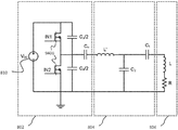
실시예에서, 무선 전력 전송 시스템은 제1복수의 파라미터를 특징으로 하는 제1발진 자기장을 통해 무선으로 수신되는 전기 에너지를 캡처하도록 구성된 적어도 하나의 수신 자기 공진기를 포함하는 무선 전력 변환기를 구비할 수 있다. 이 변환기는 또한 상기 제1복수의 파라미터와는 다른 제2복수의 파라미터를 특징으로 하는 제2발진 자기장을 생성하도록 구성된 적어도 하나의 전송 자기 공진기를 더 구비할 수 있으며, 여기서 상기 적어도 하나의 수신 자기 공진기로부터의 전기 에너지는 적어도 하나의 전송 자기 공진기를 활성화시켜 상기 제2발진 자기장을 생성하는데 사용된다. 실시예에서, 제1복수의 파라미터는 상기 제2복수의 파라미터의 제2주파수와는 다른 제1주파수를 포함할 수 있고, 제1주파수는 상기 제2주파수의 대략 정수배일 수 있다. 다른 실시예에서, 제1복수의 파라미터는 상기 제2복수의 파라미터의 제2크기와는 다른 제1크기를 포함할 수 있다. 제1복수의 파라미터는 상기 제2복수의 파라미터의 제2주파수 홉핑 시퀀스(second frequency hopping sequence)와는 다른 제1주파수 홉핑 시퀀스를 더 포함할 수 있으며, 마찬가지로, 제1복수의 파라미터는 제2복수의 파라미터의 제2온/오프 시퀀스와는 다른 제1온/오프 시퀀스를 포함할 수 있다.In an embodiment, the wireless power transfer system can include a wireless power converter including at least one receiving magnetic resonator configured to capture electrical energy received wirelessly through a first oscillating magnetic field characterized by a first plurality of parameters. have. The transducer may also further comprise at least one transmitting magnetic resonator configured to generate a second oscillating magnetic field characterized by a second plurality of parameters different from the first plurality of parameters, wherein the at least one receiving magnetic field. Electrical energy from the resonator is used to activate at least one transmitting magnetic resonator to produce the second oscillating magnetic field. In an embodiment, the first plurality of parameters may comprise a first frequency different from the second frequency of the second plurality of parameters, and the first frequency may be approximately an integer multiple of the second frequency. In another embodiment, the first plurality of parameters may include a first size different from the second size of the second plurality of parameters. The first plurality of parameters may further include a first frequency hopping sequence that is different from the second frequency hopping sequence of the second plurality of parameters, and likewise, the first plurality of parameters may include a second plurality of parameters. A first on / off sequence different from the second on / off sequence of the parameter may be included.
다른 실시예에서, 무선 전력 전송 시스템은 제1복수의 파라미터를 특징으로 하는 제1발진 자기장을 생성하도록 구성된 소스 공진기와, 상기 제1복수의 파라미터와는 다른 제2복수의 파라미터를 특징으로 하는 제2발진 자기장을 통해 무선으로 수신된 전기 에너지를 캡처하도록 구성된 디바이스 공진기를 포함할 수 있다. 시스템에서, 변환 회로를 포함하는 무선 전력 변환기는 제2발진 자기장으로부터 에너지를 캡처하고 소스 공진기를 활성화시켜 제1발진 자기장을 생성하도록 구성되고 사용될 수 있다. 실시예에서, 제1복수의 파라미터는 제2복수의 파라미터의 제2주파수와는 다른 제1주파수를 포함할 수 있으며, 제1주파수는 제2주파수의 대략 정수배일 수 있다. 다른 실시예에서, 제1복수의 파라미터는 제2복수의 파라미터의 제2크기와는 다른 제1크기를 포함할 수 있다. 제1복수의 파라미터는 또한 제2복수의 파라미터의 제2주파수 홉핑 시퀀스와는 다른 제1주파수 홉핑 시퀀스를 더 포함할 수 있으며, 마찬가지로 제1복수의 파라미터는 제2복수의 파라미터의 제2온/오프 시퀀스와는 다른 제1온/오프 시퀀스를 포함할 수 있다.In another embodiment, a wireless power transfer system includes a source resonator configured to generate a first oscillating magnetic field characterized by a first plurality of parameters, and a second plurality of parameters different from the first plurality of parameters. And a device resonator configured to capture electrical energy wirelessly received via the two-oscillating magnetic field. In the system, a wireless power converter including a conversion circuit can be configured and used to capture energy from the second oscillating magnetic field and activate the source resonator to generate the first oscillating magnetic field. In an embodiment, the first plurality of parameters may comprise a first frequency that is different from the second frequency of the second plurality of parameters, and the first frequency may be approximately an integer multiple of the second frequency. In another embodiment, the first plurality of parameters may comprise a first size different from the second size of the second plurality of parameters. The first plurality of parameters may also further comprise a first frequency hopping sequence that is different from the second frequency hopping sequence of the second plurality of parameters, and likewise the first plurality of parameters may include the second on / off of the second plurality of parameters. A first on / off sequence different from the off sequence may be included.
다른 실시예에서, 무선 전력 변환기는 구성가능한(configurable) 자기 공진기를 제공하는 단계, 제1복수의 파라미터를 특징으로 하는 제1발진 자기장을 캡처하도록 구성가능한 자기 공진기를 튜닝하는 단계, 상기 발진 자기장을 전기 에너지로 변환하는 단계, 상기 전기 에너지를 에너지 저장 소자에 저장된 에너지로서 저장하는 단계, 제2복수의 파라미터를 특징으로 하는 제2발진 자기장을 생성하도록 구성가능한 자기 공진기를 튜닝하는 단계, 및 저장된 에너지를 사용하여 구성가능한 자기 공진기를 활성화시켜 제2발진 자기장을 생성하는 단계에 의하여 변환하는데 사용될 수 있다.In another embodiment, a wireless power converter provides a configurable magnetic resonator, tuning a configurable magnetic resonator to capture a first oscillating magnetic field characterized by a first plurality of parameters, and adjusting the oscillating magnetic field. Converting into electrical energy, storing the electrical energy as energy stored in an energy storage element, tuning a magnetic resonator configurable to generate a second oscillating magnetic field characterized by a second plurality of parameters, and stored energy It can be used to convert by activating a configurable magnetic resonator using to generate a second oscillating magnetic field.
다른 실시예에서, 무선 전력 전송을 위한 공진기는 하나 이상의 루프를 형성하고 인덕턴스 L을 가지는 인덕터, 상기 인덕터에 연결된 원하는 전기 파라미터와 커패시턴스 C를 가지는 커패시터의 네트워크를 포함하며, 상기 네트워크는 상기 전기 파라미터의 제1온도 프로파일을 가지는 제1유형의 적어도 하나의 커패시터를 구비하며, 상기 네트워크는 상기 전기 파라미터의 제2온도 프로파일을 가지는 제2유형의 적어도 하나의 커패시터를 구비한다. 커패시터의 제1유형의 제1온도 프로파일은 단 하나의 유형의 커패시터만이 사용될 때보다 온도 변화로 인한 네트워크의 전기 파라미터의 변화가 더 적도록 제2유형의 커패시터의 제2온도 프로파일과 상보적일 수 있다. 실시예에서, 이들 파라미터는 온도 변화로 인한 상기 전기 파라미터의 변화가 실질적으로 제로(0)가 되도록 선택될 수 있다. 실시예에서, 전기 파라미터는 커패시턴스, 저항, 인덕턴스 등일 수 있다.In another embodiment, a resonator for wireless power transfer includes an inductor having one or more loops and having an inductance L, a network of capacitors having a desired electrical parameter and capacitance C coupled to the inductor, the network of the electrical parameters And at least one capacitor of a first type having a first temperature profile, wherein said network comprises at least one capacitor of a second type having a second temperature profile of said electrical parameter. The first temperature profile of the first type of capacitor may be complementary to the second temperature profile of the capacitor of the second type so that there is less change in the electrical parameters of the network due to temperature change than when only one type of capacitor is used. have. In an embodiment, these parameters may be selected such that the change in the electrical parameter due to the temperature change is substantially zero. In an embodiment, the electrical parameter can be capacitance, resistance, inductance, or the like.
실시예에서, 무선 전력 전송을 위한 공진기는 하나 이상의 루프를 형성하는 인덕터, 전기 파라미터에 대해 서로 다른 온도 프로파일을 가지는 2개 이상의 유형의 전기 부품을 포함할 수 있으며, 상기 전기 부품은 상기 인덕터에 연결된 네트워크를 형성하며, 상기 전기 부품은 상기 부품의 온도 프로파일이 상보적이고 단 하나의 유형의 부품만이 사용될 때보다 온도 변화로 인한 회로의 전기 파라미터의 변화가 더 적도록 배열된다. 실시예에서, 이 파라미터는 온도 변화로 인한 전기 파라미터의 변화가 실질적으로 제로가 되도록 선택될 수 있다. 실시예에서, 전기 파라미터는 커패시턴스, 조항, 인덕턴스 등일 수 있다.In an embodiment, the resonator for wireless power transfer may include an inductor forming one or more loops, two or more types of electrical components having different temperature profiles for electrical parameters, the electrical components connected to the inductor. The electrical components are arranged such that the temperature profile of the components is complementary and there is less variation in electrical parameters of the circuit due to temperature changes than when only one type of component is used. In an embodiment, this parameter may be selected such that the change in electrical parameter due to temperature change is substantially zero. In an embodiment, the electrical parameter can be capacitance, provision, inductance, or the like.
실시예에서, 무선 전력 전송은 전력 소스에 연결되고 발진 자기장을 생성하는 소스 하이-Q 자기 공진기, 상기 발진 자기장을 적어도 하나의 디바이스 공진기에 연결된 조명에 전력을 공급하는데 사용되는 전기 에너지로 변환하도록 구성된 적어도 하나의 디바이스 하이-Q 자기 공진기, 및 디바이스 공진기보다 더 큰 적어도 하나의 리피터 공진기를 포함할 수 있다. 리피터 공진기는 소스 공진기와 디바이스 공진기 사이에 전력 전송 효율을 개선시키도록 디바이스 공진기보다 소스 공진기로부터 더 멀리 위치될 수 있다. 이 시스템은 디바이스 공진기 위 캐비넷 내에 리피터 공진기를 배치하고 벽에 장착된 소스로부터 캐비넷보다 실질적으로 아래에 조명에 무선으로 전력을 공급하는데 사용될 수 있다. 실시예에서, 소스 공진기와 디바이스 공진기는 10㎝ 이상, 또는 20㎝ 이상 등으로 분리될 수 있다. 소스 및 디바이스 공진기는 실질적으로 동일한 공진기 주파수에 튜닝될 수 있다.In an embodiment, the wireless power transfer is configured to convert a source high-Q magnetic resonator coupled to a power source and generate an oscillating magnetic field, the oscillating magnetic field into electrical energy used to power an illumination coupled to at least one device resonator. At least one device high-Q magnetic resonator, and at least one repeater resonator larger than the device resonator. The repeater resonator may be located farther from the source resonator than the device resonator to improve power transfer efficiency between the source resonator and the device resonator. The system can be used to place a repeater resonator in a cabinet above the device resonator and wirelessly power the illumination substantially below the cabinet from a wall mounted source. In an embodiment, the source resonator and the device resonator may be separated by 10 cm or more, or 20 cm or more. The source and device resonators may be tuned to substantially the same resonator frequency.
실시예에서, 무선 전력 전송을 위한 디바이스는 하이-Q 공진기의 적어도 하나의 루프를 형성하는 전도체, 상기 전도체에 전기적으로 연결된 용량성 부품, 및 상기 전도체에 전기적으로 연결된 전력 및 제어 회로를 포함할 수 있다. 전력 및 제어 회로는 전력 및 제어 회로가 하이-Q 공진기가 발진 자기장을 수신하고 생성하는 방법을 선택하는 2개 이상의 동작 모드를 제공할 수 있다. 2개 이상의 동작 모드는 하이-Q 공진기가 소스로부터 전력을 무선으로 수신하고 전력을 수신기에 무선으로 전송하는데 사용되는 리피터 동작 모드를 포함할 수 있다. 2개 이상의 동작 모드는 하이-Q 공진기가 자기장을 생성하는데 사용되는 소스 동작 모드를 포함할 수 있다. 2개 이상의 동작 모드는 하이-Q 공진기가 발진 자기장을 전기 에너지로 변환하는데 사용되는 디바이스 동작 모드를 포함할 수 있다.In an embodiment, the device for wireless power transfer can include a conductor forming at least one loop of a high-Q resonator, a capacitive component electrically connected to the conductor, and power and control circuitry electrically connected to the conductor. have. The power and control circuit can provide two or more modes of operation in which the power and control circuit selects how a high-Q resonator receives and generates an oscillating magnetic field. The two or more modes of operation may include a repeater mode of operation wherein the high-Q resonator is used to wirelessly receive power from the source and wirelessly transmit power to the receiver. The two or more modes of operation may include a source mode of operation in which the high-Q resonator is used to generate the magnetic field. The two or more modes of operation may include a device mode of operation in which a high-Q resonator is used to convert the oscillating magnetic field into electrical energy.
실시예에서, 공진기는 하이-Q 공직기의 적어도 하나의 루프를 형성하는 전도체를 제공하는 단계, 상기 전도체에 전기적으로 연결된 용량성 부품을 제공하는 단계, 상기 전도체에 전기적으로 연결된 전력 및 제어 회로를 제공하는 단계, 상기 하이-Q 공진기의 하나 이상의 부품의 하나 이상의 동작 파라미터를 측정하는 단계, 및 상기 하나 이상의 동작 파라미터에 기초하여 상기 전력 및 제어 회로의 하나 또는 복수의 동작 모드를 선택하는 단계에 의하여 동작될 수 있다. 상기 복수의 동작 모드는 하이-Q 공진기가 소스로부터 전력을 무선으로 수신하고 전력을 수신기에 무선으로 송신하는데 사용되는 리피터 동작 모드를 포함할 수 있다. 상기 복수의 동작 모드는 하이-Q 공진기가 자기장을 생성하는데 사용되는 소스 동작 모드를 포함할 수 있다. 상기 복수의 동작 모드는 하이-Q 공진기가 발진 자기장을 전기 에너지로 변환하는데 사용되는 디바이스 동작 모드를 포함할 수 있다. 공진기는 리피터 또는 디바이스 동작 모드 동안 충전될 수 있는 배터리를 더 포함할 수 있다.In an embodiment, the resonator includes providing a conductor that forms at least one loop of a high-Q civil machine, providing a capacitive component electrically connected to the conductor, power and control circuitry electrically connected to the conductor. Providing, measuring one or more operating parameters of one or more components of the high-Q resonator, and selecting one or a plurality of operating modes of the power and control circuit based on the one or more operating parameters. Can be operated. The plurality of modes of operation may include a repeater mode of operation wherein the high-Q resonator is used to wirelessly receive power from a source and wirelessly transmit power to a receiver. The plurality of operating modes may include a source operating mode in which a high-Q resonator is used to generate a magnetic field. The plurality of operating modes may include a device operating mode in which a high-Q resonator is used to convert the oscillating magnetic field into electrical energy. The resonator may further include a battery that may be charged during the repeater or device operating mode.
다른 실시예에서, 일부 공진기는 지지판, 상기 지지판의 일측 위에 배치되고 공진기의 사이즈보다 더 큰 우수한 전도체의 시트, 상기 공진기와 상기 우수한 전도체의 시트 사이에 분리 거리를 유지하기 위한 분리기 부재, 및 상기 공진기, 분리기, 우수한 전도체 시트를 커버하고 상기 지지판에 부착되는 무손실 물질의 커버를 포함하는 인클로저(enclosure)를 구비할 수 있다. 전도체 시트는 구리, 알루미늄 등일 수 있다. 우수한 전도체 시트는 모든 측면에서 적어도 1㎝, 또는 적어도 2㎝ 또는 그 이상만큼 공진기의 사이즈를 초과할 수 있다.In another embodiment, some resonators include a support plate, a sheet of good conductor disposed on one side of the support plate and larger than the size of the resonator, a separator member for maintaining a separation distance between the resonator and the good conductor sheet, and the resonator And an enclosure including a separator, a good conductor sheet and a cover of lossless material attached to the support plate. The conductor sheet may be copper, aluminum, or the like. A good conductor sheet may exceed the size of the resonator by at least 1 cm, or at least 2 cm or more in all respects.
또 다른 실시예에서, 무선 전력 전송을 위한 공진기는 축을 따라 길이를 가지는 자성 물질(magnetic material)과, 상기 자성 물질 주위에 랩핑되어(wrapped) 상기 축에 대해 복수의 루프를 형성하는 제1전도체를 포함할 수 있으며, 상기 복수의 루프는 상기 자성 물질 위에 범위(span)를 가지며, 상기 길이는 상기 복수의 루프에 의해 생성된 다이폴 모멘트와 평행한 자성 물질의 최대 차원(dimension)이며 상기 복수의 루프의 범위는 상기 길이의 약 절반이다. 상기 공진기는 상기 전도체에 연결된 하나 이상의 커패시터 또는 인덕터를 포함할 수 있다. 일부 실시예에서, 상기 공진기의 공진 주파수는 이들 커패시터에 의해 튜닝될 수 있다.In yet another embodiment, a resonator for wireless power transfer includes a magnetic material having a length along an axis and a first conductor wrapped around the magnetic material to form a plurality of loops about the axis. Wherein the plurality of loops has a span over the magnetic material, the length is a maximum dimension of the magnetic material parallel to the dipole moment generated by the plurality of loops and the plurality of loops The range of is about half of the length. The resonator may include one or more capacitors or inductors coupled to the conductor. In some embodiments, the resonant frequency of the resonator may be tuned by these capacitors.
본 명세서에 개시된 시스템의 일 실시예는 발진 자기장을 생성하도록 구성된 적어도 하나의 하이-Q 자기 공진기를 구비하는 소스 공진기로서, 상기 소스 공진기는 디바이스 공진기를 가지는 차량에서 일정 거리를 두고 위치되는, 소스 공진기와, 상기 소스 공진기와 디바이스 공진기의 상대적 정렬에 대한 정보를 제공하는 위치지정 시스템을 포함한다.One embodiment of a system disclosed herein is a source resonator having at least one high-Q magnetic resonator configured to generate an oscillating magnetic field, the source resonator being positioned at a distance from a vehicle having a device resonator. And a positioning system that provides information about the relative alignment of the source resonator with the device resonator.
위치지정 시스템은 차량의 오퍼레이터에 상대적 정렬에 대한 정보를 디스플레이하도록 적응된 디스플레이를 포함할 수 있다. 위치지정 시스템은 카메라를 포함할 수 있다. 위치지정 시스템은 머신 비전을 사용할 수 있다.The positioning system may include a display adapted to display information about relative alignment to the operator of the vehicle. The positioning system may include a camera. The positioning system can use machine vision.
위치지정 시스템은 소스 공진기에 있는 전류를 측정할 수 있다. 위치지정 시스템은 소스 공진기에서 전류의 위상을 측정할 수 있다. 위치지정 시스템은 소스 공진기에서 전압을 측정할 수 있다. 위치지정 시스템은 소스 공진기에서 전압의 위상을 측정할 수 있다. 위치지정 시스템은 소스 공진기 또는 디바이스 공진기의 부근에서 외부 물체(foreign object)를 검출하기 위해 하나 이상의 센서를 포함할 수 있다. 소스 공진기는 외부 물체가 검출될 때 출력 전력을 감소시킬 수 있다.The positioning system can measure the current in the source resonator. The positioning system can measure the phase of the current in the source resonator. The positioning system can measure the voltage at the source resonator. The positioning system can measure the phase of the voltage at the source resonator. The positioning system may include one or more sensors to detect foreign objects in the vicinity of the source resonator or device resonator. The source resonator may reduce the output power when an external object is detected.
위치지정 시스템은 소스 공진기를 디바이스 공진기와 원하는 정렬로 이동하게 구성된 하나 이상의 기계적 액추에이터를 포함할 수 있다. 위치지정 시스템은 디바이스 공진기를 소스 공진기와 원하는 정렬로 이동하게 구성된 하나 이상의 기계적 액추에이터를 포함할 수 있다.The positioning system may include one or more mechanical actuators configured to move the source resonator to the desired resonator with the device resonator. The positioning system may include one or more mechanical actuators configured to move the device resonator in a desired alignment with the source resonator.
위치지정 시스템은 차량의 제어 시스템에 연결될 수 있고 차량의 자동화된 위치지정을 위해 제어 시스템에 제어 신호를 제공하도록 구성될 수 있다.The positioning system may be coupled to the control system of the vehicle and may be configured to provide control signals to the control system for automated positioning of the vehicle.
소스 공진기와 디바이스 공진기는 각각 Q>100의 품질 계수(quality factor)를 지닌다.The source resonator and the device resonator each have a quality factor of Q> 100.
본 명세서에 개시된 시스템은 발진 자기장을 생성하도록 구성된 적어도 하나의 소스 하이-Q 자기 공진기를 구비하는 소스 공진기로서, 상기 소스 공진기는 차량으로부터 소정 거리에 위치된, 소스 공진기, 상기 차량에 부착된 디바이스 공진기로서, 상기 디바이스 공진기는 상기 소스 공진기와 상기 디바이스 공진기가 원하는 정렬에 있을 때 발진 자기장을 통해 전력을 수신하도록 구성된 적어도 하나의 디바이스 하이-Q 자기 공진기를 구비하는, 디바이스 공진기를 포함하며, 여기서 상기 소스 공진기와 디바이스 공진기는 원하는 정렬로부터 오정렬 범위 내에 무선 전력 전송 효율을 실질적으로 유지하도록 사이즈 정해지고 배향된다.The system disclosed herein is a source resonator having at least one source high-Q magnetic resonator configured to generate an oscillating magnetic field, the source resonator being located at a distance from the vehicle, the source resonator, the device resonator attached to the vehicle Wherein the device resonator comprises a device resonator comprising at least one device high-Q magnetic resonator configured to receive power through an oscillating magnetic field when the source resonator and the device resonator are in a desired alignment, wherein the source resonator The resonator and device resonator are sized and oriented to substantially maintain wireless power transfer efficiency within a misalignment range from the desired alignment.
소스 공진기는 디바이스 공진기보다 더 클 수 있다. 소스 공진기는 디바이스 공진기보다 35% 더 클 수 있다. 소스 공진기와 디바이스 공진기는 각각 자성 물질의 적어도 하나의 축 주위에 랩핑된 전도체를 포함할 수 있으며, 소스 공진기와 디바이스 공진기 각각의 다이폴 모멘트는 소스 공진기와 디바이스 공진기가 원하는 정렬에 있을 때 차량의 가장 긴 차원과 정렬될 수 있다. 디바이스 공진기는 차량의 리세스된 부분에 통합될 수 있다. 디바이스 공진기는 능동 온도 제어부를 포함할 수 있다.The source resonator may be larger than the device resonator. The source resonator may be 35% larger than the device resonator. The source resonator and the device resonator may each include conductors wrapped around at least one axis of the magnetic material, the dipole moments of each of the source and device resonators being the longest in the vehicle when the source and device resonators are in the desired alignment. Can be aligned with the dimension. The device resonator may be integrated into the recessed portion of the vehicle. The device resonator may include an active temperature control.
능동 온도 제어부는 디바이스 공진기의 제어가능한 냉각을 제공하기 위해 차량의 냉각 시스템에 연결될 수 있다. 능동 온도 제어부는 디바이스 공진기의 제어가능한 가열을 제공하기 위해 차량의 가열 시스템에 연결될 수 있다.The active temperature control can be connected to the vehicle's cooling system to provide controllable cooling of the device resonator. The active temperature control can be connected to the heating system of the vehicle to provide controllable heating of the device resonator.
디바이스 공진기와 소스 공진기는 각각 Q>100의 품질 계수를 지닐 수 있다.The device resonator and the source resonator may each have a quality factor of Q> 100.
다른 측면에서, 시스템의 일 실시예는 무선 전력 전송을 위한 복합 공진기를 형성하도록 어레이로 배열되고 전기적으로 상호 연결된 복수의 공진기를 포함하는 장치를 구비할 수 있으며, 상기 복수의 공진기들 각각은 그 단면과 실질적으로 동일한 영역을 둘러싸는 적어도 하나의 루프를 형성하도록 그 단면 주위에 랩핑된 전도체 와이어를 가지는 자성 물질의 블록을 포함하며, 상기 복수의 공진기는 상기 복수의 공진기 각각의 다이폴 모멘트가 상기 복수의 공진기 중 각 다른 것의 다이폴 모멘트와 정렬되도록 배향된다. 장치는 어레이로 배열된 제2복수의 공진기를 더 포함할 수 있으며, 상기 제2복수의 공진기는 각각 상기 제2복수의 공진기 중 각 다른 것의 제2다이폴 모멘트와 정렬된 제2다이폴 모멘트를 구비할 수 있다. 다른 측면에서, 장치는 어레이로 배열된 제2복수의 공진기를 더 포함할 수 있으며, 상기 제2복수의 공진기는 상기 제1복수의 공진기와는 분리된 전기 회로에 서로 전기적으로 연결된다. 장치는 복합 공진기 내에 랩핑된 전도체 없이 자성 물질의 적어도 하나의 블록을 포함할 수 있다. 어레이에서 복수의 공진기 중 인접한 것 사이의 분리 거리는 어레이의 폭, 높이 및 길이의 최대치의 10퍼센트 미만일 수 있다.In another aspect, an embodiment of the system may include an apparatus including a plurality of resonators arranged in an array and electrically interconnected to form a composite resonator for wireless power transfer, each of the plurality of resonators having a cross-sectional view thereof. And a block of magnetic material having conductor wires wrapped around its cross-section to form at least one loop that surrounds substantially the same area as the plurality of resonators, wherein the plurality of resonators comprise a plurality of dipole moments of each of the plurality of resonators Oriented to align with the dipole moment of each other of the resonators. The apparatus may further comprise a second plurality of resonators arranged in an array, the second plurality of resonators each having a second dipole moment aligned with a second dipole moment of each other of the second plurality of resonators Can be. In another aspect, the apparatus may further comprise a second plurality of resonators arranged in an array, the second plurality of resonators being electrically connected to each other in an electrical circuit separate from the first plurality of resonators. The apparatus may include at least one block of magnetic material without conductors wrapped in the composite resonator. The separation distance between adjacent ones of the plurality of resonators in the array may be less than 10 percent of the maximum of the width, height, and length of the array.
또 다른 측면에서, 시스템의 일 실시예는 어레이로 배열된 자성 물질의 복수의 블록과, 복수의 전도체 와이어를 포함하는 무선 전력 전송을 위한 장치를 구비할 수 있으며, 상기 복수의 전도체 와이어 각각은 루프를 형성하도록 상기 복수의 블록 중 적어도 하나 주위에 랩핑되고 이에 의해 복수의 공진기를 형성하며, 상기 복수의 공진기는 평행한 다이폴 모멘트와 배향되고 서로 전기적으로 연결된다. 상기 복수의 전도체 와이어에 의해 형성된 복수의 루프는 실질적으로 동축일 수 있다. 상기 복수의 공진기는 복수의 갭에 의해 서로 공간적으로 분리될 수 있다. 상기 장치는 복수의 전력 및 제어 회로를 포함할 수 있으며, 상기 복수의 전력 및 제어 회로 각각은 상기 복수의 공진기의 서로 다른 것에 전기적으로 연결된다. 각 공진기는 장치의 공진 주파수와 임피던스를 설정하기 위해 어레이에 전기적으로 연결된 적어도 2개의 커패시터를 더 포함할 수 있다. In another aspect, an embodiment of a system can include a plurality of blocks of magnetic material arranged in an array and a device for wireless power transfer including a plurality of conductor wires, each of the plurality of conductor wires being looped. Wrapped around at least one of the plurality of blocks to thereby form a plurality of resonators, the plurality of resonators being oriented with parallel dipole moments and electrically connected to each other. The plurality of loops formed by the plurality of conductor wires may be substantially coaxial. The plurality of resonators may be spatially separated from each other by a plurality of gaps. The apparatus may include a plurality of power and control circuits, each of which is electrically connected to different ones of the plurality of resonators. Each resonator may further comprise at least two capacitors electrically connected to the array to set the resonant frequency and impedance of the device.
본 발명의 하나 이상의 측면에서, 통합된 자기 공진기 및 차폐물 구조는 제1측면과 제2측면을 가지는 전기 전도체 시트, 상기 전도체 시트의 제1측면의 영역을 커버하는 자성 물질의 블록, 및 제1단부와 제2단부를 각각 구비하는 복수의 전도체 와이어 세그먼트를 포함할 수 있는 것이 고려되며, 여기서 상기 와이어 세그먼트의 단부는 상기 전도체 시트의 제1측면에 있는 점들 사이에 자성 물질의 블록 위에 라우팅(routed)된다. 구조의 일부 실시예에서, 각 전도체 와이어 세그먼트는 자성 물질의 블록의 모든 측면 주위를 완전히 랩핑하지 않을 수 있고, 전도체 시트의 최대 차원은 상기 자성 물질의 블록의 최대 차원보다 더 클 수 있다. 전도체 시트는 복수의 개별적으로 절연된 전도체 세그먼트를 포함할 수 있고, 일부 실시예에서, 절연된 전도체 세그먼트는 서로 다른 상기 전도체 와이어 세그먼트를 전기적으로 연결하도록 형성될 수 있다. 다른 실시예에서, 상기 절연된 전도체 세그먼트는 직렬로 전도체 와이어 세그먼트 중 적어도 2개를 연결하도록 형성될 수 있고, 전도체 세그먼트는 자성 물질의 블록을 둘러싸는 경로를 형성하도록 형성될 수 있으며, 자성 물질의 블록에 의해 중복되지 않는 전도체 시트의 영역으로 실질적으로 한정된다. 전도체 세그먼트는 공진기의 동작 동안 전도체 세그먼트 전부에서 전기 전류 분배를 실질적으로 균등화하기 위해 사이즈 정해지고 형성되며 상호 연결될 수 있다. 나아가, 이 구조의 전도체 시트는 자성 물질의 블록에 의해 중복된 영역의 상당한 부분의 절삭부(cutout)를 포함할 수 있다. 이 구조의 자성 물질의 블록은 전도체 시트에 있는 상기 절삭부를 통해 액세스가능한 리세스된 공동(cavity)을 가지게 형성될 수 있으며, 이에 일부 실시예에서 전력 및 제어 회로의 배치를 가능하게 할 수 있다. 나아가, 전도체 와이어 세그먼트는 서로 실질적으로 평행하게 배열될 수 있다. 일부 실시예에서, 일부 전도체 와이어 세그먼트는 하나를 초과하는 자기 다이폴 모멘트를 가지는 구조를 생성하도록 실질적으로 비평행하게 배열될 수 있다. 전도체 세그먼트는 인쇄 회로 보드 위에 제조될 수 있고, 전도체 와이어 세그먼트는 리츠(Litz) 와이어를 포함할 수 있다. 구조의 전도체 와이어 세그먼트와 전도체 차폐물은 자성 물질 블록을 수용하도록 형성되고 플렉스 회로 위에 형성될 수 있다.In one or more aspects of the invention, an integrated magnetic resonator and shield structure comprises an electrical conductor sheet having a first side and a second side, a block of magnetic material covering an area of the first side of the conductor sheet, and a first end It is contemplated that it may include a plurality of conductor wire segments each having a second end and a second end, wherein an end of the wire segment is routed over a block of magnetic material between points on the first side of the conductor sheet. do. In some embodiments of the structure, each conductor wire segment may not completely wrap around all sides of the block of magnetic material, and the maximum dimension of the conductor sheet may be greater than the maximum dimension of the block of magnetic material. The conductor sheet may include a plurality of individually insulated conductor segments, and in some embodiments, the insulated conductor segments may be formed to electrically connect the different conductor wire segments to each other. In another embodiment, the insulated conductor segment may be formed to connect at least two of the conductor wire segments in series, the conductor segment may be formed to form a path surrounding the block of magnetic material, It is substantially defined by the area of the conductor sheet not overlapped by the block. The conductor segments may be sized, formed and interconnected to substantially equalize the electrical current distribution in all of the conductor segments during operation of the resonator. Furthermore, the conductor sheet of this structure may include a cutout of a substantial portion of the area overlapped by a block of magnetic material. Blocks of magnetic material of this structure may be formed with recessed cavities accessible through the cut in the conductor sheet, which in some embodiments may enable placement of power and control circuitry. Furthermore, the conductor wire segments can be arranged substantially parallel to each other. In some embodiments, some conductor wire segments may be arranged substantially non-parallel to produce a structure having more than one magnetic dipole moment. The conductor segment can be fabricated on a printed circuit board, and the conductor wire segment can comprise Litz wire. The conductor wire segment and conductor shield of the structure can be formed to receive a block of magnetic material and can be formed over the flex circuit.
본 발명의 더 다른 측면에서, 통합된 자기 공진기와 차폐물 구조는 전기 전도체 시트, 상기 전도체 시트의 영역과 중복하고 이를 커버하는 전도체 시트의 제1위에 위치된 자성 물질 블록, 및 복수의 전도체 와이어 세그먼트를 포함할 수 있는 것으로 고려되며, 여기서 상기 와이어 세그먼트의 단부들은 상기 전도체 시트의 별개의 점들에 연결되고 상기 전도체 와이어 세그먼트는 자성 물질 블록 위에 라우팅되며, 상기 전도체 차폐물은 상기 공진기의 동작 동안 전도체 와이어 세그먼트를 위한 전류 경로로서 사용된다.In still another aspect of the invention, an integrated magnetic resonator and shield structure includes an electrical conductor sheet, a magnetic material block located on a first portion of the conductor sheet that overlaps and covers an area of the conductor sheet, and a plurality of conductor wire segments. Wherein the ends of the wire segment are connected to separate points of the conductor sheet and the conductor wire segment is routed over a block of magnetic material, and the conductor shield connects the conductor wire segment during operation of the resonator. It is used as a current path for
일 실시예에서, 공진기의 자성 물질의 타일이 공진기의 다이폴 모멘트와 실질적으로 수직인 타일 심(tile seam) 또는 조인트(joint)의 수를 최소화하도록 배열될 수 있다. 다른 측면에서, 열 전도체가 자성 물질의 타일과 접촉하게 위치될 수 있고, 공진기의 다이폴 모멘트와 실질적으로 수직하게 배향될 수 있다. 열 전도체는 대류, 전도 또는 복사를 통해 열 전도체에 의해 전달되는 열을 발산하는 추가적인 히트싱크(heatsink)에 연결될 수 있다. 더 작은 타일의 자성 물질로 구성된 자성 물질의 블록을 포함하는 공진기에서, 열 전도체는 바람직하게는 공진기의 다이폴 모멘트에 수직인 타일들, 특히 심들 사이에 심을 커버하도록 위치된다. In one embodiment, tiles of magnetic material of the resonator may be arranged to minimize the number of tile seams or joints that are substantially perpendicular to the dipole moment of the resonator. In another aspect, the thermal conductor can be positioned in contact with a tile of magnetic material and oriented substantially perpendicular to the dipole moment of the resonator. The thermal conductors may be connected to additional heatsinks that dissipate heat transferred by the thermal conductors through convection, conduction or radiation. In a resonator comprising a block of magnetic material composed of a smaller tile of magnetic material, the thermal conductor is preferably positioned to cover the shim between the tiles, in particular the shims, perpendicular to the dipole moment of the resonator.
실시예에서, 무선 전력 전송을 위해 적응된 시스템에서, 튜닝가능한 공진 증폭기 회로는 가변 임피던스를 가지는 유도성 부하를 구동하게 제공될 수 있고, 상기 회로는, 가변 듀티 사이클을 구비하는 스위칭 증폭기, 상기 유도성 부하, 상기 유도성 부하와 상기 스위칭 증폭기 사이에 적어도 하나의 튜닝가능한 부품을 포함하는 연결부, 상기 적어도 하나의 튜닝 가능한 부품과 증폭기의 듀티 사이클을 조절하기 위한 피드백 루프를 포함하며, 여기서 상기 피드백 루프는 상기 증폭기의 듀티 사이클을 조절하고 상기 적어도 하나의 튜닝 가능한 부품을 조절하여 유도성 부하의 여러 부하 상태 하에서 상기 증폭기의 출력에서 전압 스위칭이 실질적으로 0으로 유지하고 전류 스위칭이 실질적으로 0으로 유지하게 한다. 상기 적어도 하나의 튜닝 가능한 부품은 튜닝가능한 커패시터를 포함할 수 있다. 튜닝 가능한 커패시터는 유도성 부하와 직렬일 수 있다. 튜닝가능한 커패시터는 유도성 부하와 병렬 일 수 있다. 유도성 부하와 스위칭 증폭기 사이에 연결부는 하나를 초과하는 튜닝가능한 부품을 포함할 수 있다. 스위칭 증폭기는 가변 스위칭 주파수를 사용할 수 있다. 스위칭 증폭기의 버스 전압은 가변적일 수 있고 유도성 부하에 전달되는 전력의 양을 제어하는데 사용될 수 있다. 피드백 루프는 임피던스 측정 설비를 포함할 수 있다. 피드백 루프는 프로세서를 포함할 수 있고, 상기 프로세서는 스위칭 증폭기의 출력에서 임피던스를 모니터링하도록 구성되고 상기 전압 스위칭이 실질적으로 0으로 유지되도록 스위칭 증폭기의 가변 듀티 사이클에 대한 조절량을 계산하도록 구성된다. 이 프로세서는 전류 스위칭이 0으로 실질적으로 유지되도록 적어도 하나의 튜닝 가능한 부품에 대해 제2조절량을 계산하도록 구성될 수 있다. 유도성 부하는 하이-Q 자기 공진기를 포함할 수 있다. 회로는 무선 전력 송신 시스템에서 소스로서 사용될 수 있다.In an embodiment, in a system adapted for wireless power transfer, a tunable resonant amplifier circuit may be provided to drive an inductive load having a variable impedance, the circuit comprising: a switching amplifier having a variable duty cycle, the induction And a feedback loop comprising a sexual load, a connection including at least one tunable component between the inductive load and the switching amplifier, and a feedback loop for adjusting the duty cycle of the at least one tunable component and the amplifier. Regulates the duty cycle of the amplifier and adjusts the at least one tunable component such that voltage switching remains substantially zero and current switching remains substantially zero at the output of the amplifier under different load conditions of an inductive load. do. The at least one tunable component may comprise a tunable capacitor. The tunable capacitor can be in series with an inductive load. The tunable capacitor can be in parallel with the inductive load. The connection between the inductive load and the switching amplifier may include more than one tunable component. The switching amplifier may use a variable switching frequency. The bus voltage of the switching amplifier can be variable and can be used to control the amount of power delivered to the inductive load. The feedback loop may include an impedance measurement facility. The feedback loop may comprise a processor, the processor configured to monitor the impedance at the output of the switching amplifier and to calculate an adjustment amount for a variable duty cycle of the switching amplifier such that the voltage switching remains substantially zero. The processor may be configured to calculate a second adjustment amount for the at least one tunable component such that current switching remains substantially zero. Inductive loads may include high-Q magnetic resonators. The circuit can be used as a source in a wireless power transmission system.
실시예에서, 무선 전력 전송 설비에서 공진 증폭기 회로를 튜닝하는 방법은 가변 임피던스를 구비하는 유도성 부하와 스위칭 증폭기 사이에 연결부를 포함하는 것으로 제공될 수 있으며, 상기 방법은, 상기 스위칭 증폭기의 출력에서 다수의 파라미터를 측정하는 단계; 상기 스위칭 증폭기의 듀티 사이클을 조절하는 단계; 및 상기 스위칭 증폭기와 유도성 부하 사이에 연결부에서 적어도 하나의 튜닝가능한 부품을 조절하는 단계를 포함하며, 상기 스위칭 증폭기의 듀티 사이클을 조절하는 단계와 상기 적어도 하나의 튜닝가능한 부품을 조절하는 단계는 유도성 부하의 여러 부하 상태 하에서 스위칭 증폭기의 출력에서 전압 스위칭이 실질적으로 0을 유지하고 전류 스위칭이 실질적으로 0을 유지하도록 제어된다. 적어도 하나의 튜닝가능한 부품은 튜닝가능한 커패시터를 포함할 수 있다. 다수의 파라미터를 측정하는 단계는 스위칭 증폭기의 출력에서 임피던스를 측정하는 단계를 포함할 수 있다. 나아가, 스위칭 증폭기의 듀티 사이클에 대한 필요한 조절과 적어도 하나의 튜닝가능한 부품에 대한 조절을 계산하는 것은 스위칭 증폭기의 출력에서 전압을 실질적으로 0으로 유지하고 전류 스위칭을 실질적으로 0으로 유지하도록 임피던스에 기초할 수 있다. 유도성 부하와, 스위칭 증폭기와 유도성 부하 사이에 연결부의 적어도 일부분은 하이-Q 자기 공진기를 형성할 수 있다. 이 회로는 무선 전력 송신 시스템에서 소스로서 사용될 수 있다.In an embodiment, a method of tuning a resonant amplifier circuit in a wireless power transmission facility may be provided comprising a connection between an inductive load having a variable impedance and a switching amplifier, wherein the method comprises: at the output of the switching amplifier. Measuring a plurality of parameters; Adjusting the duty cycle of the switching amplifier; And adjusting at least one tunable component at a connection between the switching amplifier and an inductive load, wherein adjusting the duty cycle of the switching amplifier and adjusting the at least one tunable component are inductive. Under various load conditions of the star load, the voltage switching at the output of the switching amplifier is controlled to be substantially zero and the current switching is kept substantially zero. At least one tunable component can include a tunable capacitor. Measuring the plurality of parameters may include measuring impedance at the output of the switching amplifier. Further, calculating the necessary adjustments to the duty cycle of the switching amplifier and the adjustment to the at least one tunable component is based on the impedance to keep the voltage at substantially zero and the current switching at substantially zero at the output of the switching amplifier. can do. At least a portion of the connection between the inductive load and the switching amplifier and the inductive load may form a high-Q magnetic resonator. This circuit can be used as a source in a wireless power transmission system.
본 개시 내용은 커패시터, 인덕터, 저항, 다이오드, 변압기, 스위치 등과 같은 특정 개별 회로 부품 및 소자; 네트워크, 위상, 회로 등과 같은 이들 소자의 조합; 및 전체 물체를 통해 분배된(또는 단독 덩어리와는 대조적으로 부분적으로 분산된) 커패시턴스 또는 인덕턴스를 가지는 "자기 공명" 물체와 같은 고유한 특성을 가지는 물체를 참조한다. 이 기술 분야에 통상의 지식을 가진 자라면 회로 또는 네트워크 내에서 가변 부품을 조절하고 제어하는 것이 이 회로 또는 네트워크의 성능을 조절할 수 있고 이 조절은 일반적으로 튜닝, 조절, 매칭, 정정 등으로 기술될 수 있다는 것을 이해할 수 있을 것이다. 무선 전력 전송 시스템의 동작 점을 튜닝하거나 조절하는 다른 방법은 단독으로 사용될 수 있고 또는 인덕터와 커패시터 또는 인덕터와 커패시터의 뱅크와 같은 튜닝가능한 부품을 조절하는 것에 더하여 사용될 수 있다. 이 기술 분야에 통상의 지식을 가진 자라면 본 개시 내용에 설명된 특정 위상이 여러 다른 방식으로 구현될 수 있다는 것을 인식할 수 있을 것이다.The present disclosure provides specific discrete circuit components and devices such as capacitors, inductors, resistors, diodes, transformers, switches, and the like; Combinations of these devices, such as networks, topologies, circuits, and the like; And an object having inherent properties such as a "magnetic resonance" object having capacitance or inductance distributed throughout the whole object (or partially dispersed in contrast to a single mass). Those skilled in the art will appreciate that adjusting and controlling the variable components within the circuit or network can control the performance of the circuit or network and this adjustment is generally described as tuning, tuning, matching, correction, etc. I can understand that you can. Other methods of tuning or adjusting the operating point of the wireless power transfer system may be used alone or in addition to adjusting the tunable components, such as inductors and capacitors or banks of inductors and capacitors. Those skilled in the art will appreciate that the specific phases described in this disclosure can be implemented in many different ways.
달리 한정되지 않는 한, 본 명세서에 사용된 모든 기술적 및 과학적 용어들은 본 발명이 속하는 이 기술 분야에 통상의 지식을 가진 자에게 일반적으로 이해되는 바와 같은 의미를 가진다. 본 명세서에 참조 문헌으로 언급되거나 병합된 공개 공보, 특허 출원, 특허 공보, 및 다른 참조 문헌과 충돌시에는 정의를 포함하여 본 명세서가 우선한다.Unless defined otherwise, all technical and scientific terms used herein have the same meaning as commonly understood by one of ordinary skill in the art to which this invention belongs. In case of conflict with the publications, patent applications, patent publications, and other references mentioned or incorporated herein by reference, this specification, including definitions, takes precedence.
전술된 특징들 중 어느 것도 본 발명의 범위를 벗어남이 없이 단독으로 또는 조합하여 사용될 수 있다. 본 명세서에 개시된 시스템과 방법의 다른 특징, 목적 및 이점은 이하 상세한 설명과 도면으로부터 명백할 것이다.Any of the above features may be used alone or in combination without departing from the scope of the invention. Other features, objects, and advantages of the systems and methods disclosed herein will be apparent from the following detailed description and drawings.
도 1은 무선 에너지 전송 구성의 시스템 블록도;
도 2a 내지 도 2f는 간단한 공진기 구조의 예시적인 구조 및 개략도;
도 3은 싱글 엔디드(single-ended) 증폭기를 가지는 무선 소스의 블록도;
도 4는 차동 증폭기를 가지는 무선 소스의 블록도;
도 5a 및 도 5b는 센싱 회로의 블록도;
도 6a, 도 6b 및 도 6c는 무선 소스의 블록도;
도 7은 증폭기의 파라미터에 대한 듀티 사이클의 효과를 도시하는 그래프;
도 8은 스위칭 증폭기를 가지는 무선 전력 소스의 간략화된 회로도;
도 9는 무선 전력 소스의 파라미터의 변화 효과를 도시하는 그래프;
도 10은 무선 전력 소스의 파라미터의 변화 효과를 도시하는 그래프;
도 11a, 도 11b 및 도 11c는 무선 전력 소스의 파라미터의 변화 효과를 도시하는 그래프;
도 12는 무선 전력 소스의 파라미터의 변화 효과를 도시하는 그래프;
도 13은 무선 전력 디바이스와 스위칭 증폭기를 가지는 무선 전력 소스를 구비하는 무선 에너지 전송 시스템의 간략화된 회로도;
도 14는 무선 전력 소스의 파라미터의 변화 효과를 도시하는 그래프;
도 15는 자성 물질의 타일들 사이에 불규칙적인 간격으로 인해 비균일한 자기장 분포를 도시하는 공진기를 도시하는 도면;
도 16은 자성 물질 블록에서 핫스팟을 감소시킬 수 있는 자성 물질의 블록에서 타일의 배열을 가지는 공진기를 도시하는 도면;
도 17a는 더 작은 개별 타일을 구비하는 자성 물질 블록을 가지는 공진기를 도시하는 도면;
도 17b 및 도 17c는 열을 관리하는데 사용되는 열 전도 물질의 추가적인 스트립을 가지는 공진기를 도시하는 도면;
도 18a 및 도 18b는 리피터 공진기를 구비하는 공진기 구성을 도시하는 도면;
도 19a 및 도 19b는 리피터 공진기를 구비하는 공진기 구성을 도시하는 도면;
도 20a는 2개의 리피터 공진기를 가지는 구성을 도시하는 도면;
도 20b는 리피터 공진기로 동작하는 디바이스 공진기를 가지는 공진기 구성을 도시하는 도면;
도 21은 리피터 공진기를 구비하는 캐비넷 아래 도명 응용을 도시하는 도면;
도 22는 전기 콘센트 커버에 통합된 소스 공진기를 도시하는 도면;
도 23은 공진기 인클로저의 분해도;
도 24a는 하측에 장착된 디바이스 공진기를 가지는 차량을 도시하는 도면;
도 24b는 매트에 통합된 소스 공진기를 도시하는 도면;
도 24c는 매트와 통합된 소스와 디바이스 공진기를 가지는 차량을 도시하는 도면;
도 24d는 하측에 장착된 디바이스 공진기를 가지는 로봇을 도시하는 도면;
도 25는 하나의 세라믹 커패시터의 온도로 인해 커패시턴스 변화를 도시하는 그래프;
도 26a는 수동 보상에 사용될 수 있는 2개의 부품의 예시적인 커패시턴스 대 온도 프로파일을 도시하는 도면;
도 26b는 수동 보상에 사용될 수 있는 3개의 부품의 예시적인 커패시턴스 대 온도 프로파일을 도시하는 도면;
도 27a는 전도체의 범위를 도시하는 공진기를 도시하는 도면;
도 27b는 중공 구획을 가지는 공진기의 단면을 도시하는 도면;
도 28a는 플랩을 구비하는 전도체 차폐물을 가지는 공진기의 사시도;
도 28b는 플랩을 구비하는 전도체 차폐물을 가지는 공진기의 측면도;
도 29는 데스크 환경을 가지는 리피터 공진기를 사용하는 시스템을 도시하는 도면;
도 30은 다수의 모드에서 동작될 수 있는 공진기를 사용하는 시스템을 도시하는 도면;
도 31은 다수의 동작 모드를 가지게 구성된 공진기의 전력 및 제어 회로의 회로 블록도;
도 32a는 무선 전력 변환기를 사용하는 시스템의 구성의 블록도;
도 32b는 리피터로 기능할 수 있는 무선 전력 변환기를 사용하는 시스템의 구성의 블록도;
도 33은 무선 전력 변환기의 여러 구성 및 사용을 도시하는 블록도;
도 34a는 2개의 별개의 공진기 및 AC-DC 변환기를 사용하는 무선 전력 변환기의 블록도;
도 34b는 2개의 별개의 공진기 및 AC-AC 변환기를 사용하는 무선 전력 변환기의 블록도;
도 35는 하나의 공진기를 사용하는 무선 전력 변환기의 회로 블록도;
도 36a 및 도 36b는 상이한 사이즈의 공진기를 가지는 무선 전력 변환기를 사용하는 시스템 구성의 회로도;
도 37은 차량의 측방향 측방향 변위 또는 좌우(side to side) 위치지정 불확실성을 가능하게 하도록 상대적 소스 및 디바이스 공진기 차원을 도시하는 도면;
도 38a는 자성 물질의 단일 블록을 구비하는 공진기를 도시하는 도면;
도 38b, 도 38c, 도 38d는 자성 물질의 다수의 별개의 블록을 구비하는 공진기를 도시하는 도면;
도 39a, 도 39b, 도 39c는 하나 및 하나를 초과하는 자성 물질의 별개의 블록을 구비하는 공진기들 사이에 무선 전력 전송 특성을 비교하는데 사용되는 공진기 구성의 사시도;
도 40은 전도체로 각각 랩핑된 자성 물질의 4개의 별개의 블록을 구비하는 공진기의 사시도;
도 41a는 지그재그로 배열된 전도체 권선을 가지는 자성 물질의 2개의 블록을 구비하는 공진기를 도시하는 평면도;
도 41b는 자성 물질의 2개의 블록 사이에 공간을 감소시키도록 형성된 자성 물질의 2개의 블록을 구비하는 공진기를 도시하는 평면도;
도 42a는 전도체 차폐물을 가지는 공진기의 사시도;
도 42b는 통합된 전도체 차폐물을 가지는 공진기의 일 실시예의 사시도;
도 42c는 개별 전도체 세그먼트를 가지는 통합된 전도체 차폐물을 가지는 공진기의 사시도;
도 43a, 도 43b, 도 43c는 통합된 공진기-차폐물 구조의 일 실시예의 평면도, 측면도 및 정면도를 각각 도시하는 도면;
도 44는 통합된 공진기-차폐물 구조의 일 실시예의 분해도;
도 45a는 전도체 차폐물에 대해 대칭적인 전도체 세그먼트를 가지는 통합된 공진기-차폐물 구조의 일 실시예를 도시하는 평면도;
도 45b는 통합된 공진기-차폐물 구조의 다른 실시예의 사시도;
도 46a는 자성 물질의 블록에 공동을 가지는 통합된 공진기-차폐물 구조의 사시도;
도 46b는 통합된 공진기-차폐물 구조의 전도체 부품의 일 실시예의 사시도;
도 47은 2개의 다이폴 모멘트를 가지는 통합된 공진기-차폐물 구조의 일 실시예의 사시도;
도 48은 수술 로봇과 병원 침대로 무선 에너지 전송을 하는 응용을 도시하는 도면;
도 49는 수술 로봇과 병원 침대로 무선 에너지 전송을 하는 응용을 도시하는 도면;
도 50a는 무선 에너지 전송을 하는 의료 카트의 일 실시예를 도시하는 도면;
도 50b는 무선 에너지 전송을 하는 컴퓨터 카트의 일 실시예를 도시하는 도면.1 is a system block diagram of a wireless energy transfer configuration;
2A-2F are exemplary structures and schematic diagrams of a simple resonator structure;
3 is a block diagram of a wireless source having a single-ended amplifier;
4 is a block diagram of a wireless source having a differential amplifier;
5A and 5B are block diagrams of sensing circuits;
6A, 6B and 6C are block diagrams of a wireless source;
7 is a graph showing the effect of duty cycle on the parameters of an amplifier;
8 is a simplified circuit diagram of a wireless power source having a switching amplifier;
9 is a graph illustrating the effect of changing a parameter of a wireless power source;
10 is a graph showing the effect of changing a parameter of a wireless power source;
11A, 11B and 11C are graphs illustrating the effect of changing the parameters of the wireless power source;
12 is a graph illustrating the effect of changing a parameter of a wireless power source;
13 is a simplified circuit diagram of a wireless energy transfer system having a wireless power source having a wireless power device and a switching amplifier;
14 is a graph showing the effect of changing a parameter of a wireless power source;
FIG. 15 shows a resonator showing non-uniform magnetic field distribution due to irregular spacing between tiles of magnetic material;
FIG. 16 shows a resonator having an arrangement of tiles in a block of magnetic material that can reduce hot spots in the block of magnetic material; FIG.
FIG. 17A shows a resonator having a block of magnetic material having smaller individual tiles; FIG.
17B and 17C illustrate resonators with additional strips of thermally conductive material used to manage heat;
18A and 18B show a resonator configuration having a repeater resonator;
19A and 19B show a resonator configuration having a repeater resonator;
20A is a diagram illustrating a configuration having two repeater resonators;
20B shows a resonator configuration having a device resonator acting as a repeater resonator;
FIG. 21 illustrates a lighting application under a cabinet having a repeater resonator; FIG.
FIG. 22 shows a source resonator integrated into an electrical outlet cover; FIG.
23 is an exploded view of a resonator enclosure;
FIG. 24A shows a vehicle having a device resonator mounted below;
24B shows a source resonator integrated into the mat;
FIG. 24C shows a vehicle having a source and device resonator integrated with a mat; FIG.
24D shows a robot with a device resonator mounted on the bottom;
25 is a graph showing capacitance change due to temperature of one ceramic capacitor;
FIG. 26A shows an example capacitance versus temperature profile of two components that can be used for passive compensation; FIG.
FIG. 26B shows an example capacitance versus temperature profile of three components that can be used for passive compensation; FIG.
27A shows a resonator showing the range of conductors;
27B shows a cross section of a resonator having a hollow compartment;
28A is a perspective view of a resonator having a conductor shield with flaps;
FIG. 28B is a side view of a resonator having conductor shields with flaps; FIG.
29 illustrates a system using a repeater resonator having a desk environment;
30 illustrates a system using a resonator that can be operated in multiple modes;
31 is a circuit block diagram of a power and control circuit of a resonator configured to have multiple modes of operation.
32A is a block diagram of a configuration of a system using a wireless power converter.
32B is a block diagram of a configuration of a system using a wireless power converter that can function as a repeater;
33 is a block diagram illustrating various configurations and uses of a wireless power converter.
34A is a block diagram of a wireless power converter using two separate resonators and an AC-DC converter.
34B is a block diagram of a wireless power converter using two separate resonators and an AC-AC converter.
35 is a circuit block diagram of a wireless power converter using one resonator;
36A and 36B are circuit diagrams of a system configuration using wireless power converters having resonators of different sizes;
FIG. 37 illustrates relative source and device resonator dimensions to enable lateral lateral displacement or side to side positioning uncertainty of the vehicle; FIG.
38A illustrates a resonator having a single block of magnetic material;
38B, 38C, and 38D illustrate resonators having multiple discrete blocks of magnetic material;
39A, 39B, 39C are perspective views of resonator configurations used to compare wireless power transfer characteristics between resonators having one and more than one separate block of magnetic material;
40 is a perspective view of a resonator having four separate blocks of magnetic material each wrapped with a conductor;
41A is a plan view showing a resonator having two blocks of magnetic material having zigzag conductor windings;
41B is a plan view showing a resonator having two blocks of magnetic material formed to reduce the space between two blocks of magnetic material;
42A is a perspective view of a resonator having conductor shields;
42B is a perspective view of one embodiment of a resonator having an integrated conductor shield;
42C is a perspective view of a resonator having an integrated conductor shield having individual conductor segments;
43A, 43B, 43C show top, side, and front views, respectively, of one embodiment of an integrated resonator-shield structure;
44 is an exploded view of one embodiment of an integrated resonator-shield structure;
45A is a plan view illustrating one embodiment of an integrated resonator-shield structure having conductor segments symmetrical about the conductor shield;
45B is a perspective view of another embodiment of an integrated resonator-shield structure;
46A is a perspective view of an integrated resonator-shield structure having a cavity in a block of magnetic material;
46B is a perspective view of one embodiment of a conductor component of an integrated resonator-shield structure;
47 is a perspective view of one embodiment of an integrated resonator-shield structure with two dipole moments;
48 illustrates an application for wireless energy transfer to a surgical robot and a hospital bed;
FIG. 49 illustrates an application for wireless energy transfer to a surgical robot and hospital bed; FIG.
50A illustrates one embodiment of a medical cart for wireless energy transfer;
50B illustrates an embodiment of a computer cart for wireless energy transfer.
전술된 바와 같이, 본 발명은 결합된 전자기 공진기를 사용하여 무선 에너지를 전송하는 것에 관한 것이다. 그러나, 이러한 에너지 전송은 전자기 공진기로 제한되지 않으며 본 명세서에 기술된 무선 에너지 전송 시스템은 보다 일반적이고 광범위한 공진기와 공진기 물체를 사용하여 구현될 수 있다.As mentioned above, the present invention relates to the transmission of wireless energy using a coupled electromagnetic resonator. However, such energy transfer is not limited to electromagnetic resonators and the wireless energy transfer system described herein can be implemented using a more general and wider range of resonator and resonator objects.
이 기술 분야에 통상의 지식을 가진 자라면 인식할 수 있는 바와 같이, 공진기 기반 전력 전송을 위한 중요한 고려사항은 공진기 효율과 공진기 결합을 포함한다. 이 문제, 예를 들어, 결합된 모드 이론(CMT), 결합 계수 및 계수, 품질 계수(또는 Q 계수라고도 지칭됨) 및 임피던스 매칭에 대한 광범위한 논의는 그 전체 내용이 본 명세서에 완전히 기재된 것처럼 병합된, 예를 들어, 미국 특허 출원 제12/789,611호(이는 2010년 9월 23일에 미국 특허 공개 제20100237709호로 공개됨, 발명의 명칭: "RESONATOR ARRAYS FOR WIRELESS ENERGY TRANSFER") 및 미국 특허 출원 제12/722,050호(이는 2010년 7월 22일에 미국 특허 공개 제20100181843호로 공개됨, 발명의 명칭: "WIRELESS ENERGY TRANSFER FOR REFRIGERATOR APPLICATION")에 제공된다.As one of ordinary skill in the art will appreciate, important considerations for resonator based power transfer include resonator efficiency and resonator coupling. Extensive discussion of this problem, eg, combined mode theory (CMT), coupling coefficients and coefficients, quality coefficients (also called Q coefficients), and impedance matching have been incorporated as if the entirety were fully described herein. US Patent Application No. 12 / 789,611, which is published on September 23, 2010, US Patent Publication No. 20100237709, entitled “RESONATOR ARRAYS FOR WIRELESS ENERGY TRANSFER” and US Patent Application No. 12 / 722,050, which is published as US Patent Publication No. 20100181843 on July 22, 2010, entitled "WIRELESS ENERGY TRANSFER FOR REFRIGERATOR APPLICATION."
공진기는 적어도 2개의 상이한 형태로 에너지를 저장할 수 있고 2개의 형태 사이에서 저장된 에너지가 발진 공진 구조로 한정될 수 있다. 공진 구조는 공진 (모드) 주파수(f) 및 공진 (모드) 장을 가지는 특정 발진 모드를 가질 수 있다. 각도 공진 주파수(ω)는 ω = 2πf로서 정의될 수 있으며, 공진 주기(T)는 T=1/f=2π/ω로서 정의될 수 있으며, 공진 파장(λ)은 λ=c/f 로서 정의될 수 있으며, 여기서 c는 연관된 장의 파(associated field wave)(전자기 공진기에 대해서는 광)의 속도이다. 손실 메커니즘, 결합 메커니즘 또는 외부 에너지 공급 또는 드레인 메커니즘이 없으면, 공진기에 의해 저장되는 에너지의 총 양(W)은 고정되게 유지될 수 있으나, 에너지의 형태는 공진기에 의해 지지되는 2개의 형태 사이에 발진할 수 있으며, 여기서 하나의 형태는 다른 형태가 최소화될 때 최대가 되고 또 그 반대로도 된다.The resonator may store energy in at least two different forms and the energy stored between the two forms may be defined by an oscillating resonant structure. The resonant structure may have a specific oscillation mode having a resonant (mode) frequency f and a resonant (mode) field. The angular resonance frequency ω may be defined as ω = 2πf, the resonance period T may be defined as T = 1 / f = 2π / ω, and the resonance wavelength λ is defined as λ = c / f. Where c is the velocity of the associated field wave (light for an electromagnetic resonator). Without a loss mechanism, coupling mechanism, or external energy supply or drain mechanism, the total amount of energy (W) stored by the resonator can remain fixed, but the form of energy oscillates between the two forms supported by the resonator. Where one form is maximal when the other is minimized and vice versa.
예를 들어, 공진기는 저장된 에너지의 2개의 형태가 자기 에너지 및 전기 에너지가 되도록 구성될 수 있다. 나아가, 공진기는 전기장에 의해 저장된 전기 에너지가 기본적으로 구조 내에서 한정되는 반면 자기장에 의해 저장된 자기 에너지는 기본적으로 공진기를 둘러싸는 영역에 있도록 구성될 수 있다. 다시 말해, 총 전기 및 자기 에너지는 동일할 수 있으나, 그 국부화는 다를 수 있다. 이 구조를 사용하면 적어도 2개의 구조들 사이에 에너지 교환이 적어도 2개의 공진기의 공진 자기 근접장에 의해 중개될 수 있다. 이들 유형의 공진기는 자기 공진기라고 지칭될 수 있다.For example, the resonator may be configured such that two forms of stored energy are magnetic energy and electrical energy. Furthermore, the resonator may be configured such that the electrical energy stored by the electric field is basically limited in the structure while the magnetic energy stored by the magnetic field is basically in the region surrounding the resonator. In other words, the total electrical and magnetic energy may be the same, but their localization may be different. Using this structure, energy exchange between the at least two structures can be mediated by the resonant magnetic near field of the at least two resonators. These types of resonators may be referred to as magnetic resonators.
무선 전력 송신 시스템에서 사용되는 공진기의 중요한 파라미터는 에너지 감쇠를 특징으로 하고 공진기의 에너지 손실에 반비례하는 품질 계수, 또는 Q 계수 또는 Q이다. 이 Q는 Q=ω*W/P로 정의될 수 있으며, 여기서 P는 안정 상태에서 손실되는 시간 평균된 전력이다. 즉, 하이 Q를 가지는 공진기는 상대적으로 낮은 내재 손실을 가지며 상대적으로 긴 시간 동안 에너지를 저장할 수 있다. 공진기가 내재 감쇠율(2Γ)에서 에너지를 손실하므로, 내재 Q라고도 지칭되는 Q는 Q=ω/2Γ에 의해 주어진다. 이 품질 계수는 또한 공진기에서 에너지가 e-2π의 계수만큼 감쇠하는데 드는 발진 기간(T)의 수를 나타낸다. 공진기의 품질 계수 또는 내재 품질 계수 또는 Q는 단지 내재 손실 메커니즘으로 인한 것이라는 것을 주목해야 한다. 전력 생성기(g), 또는 부하(ℓ)에 연결되거나 결합된 공진기의 Q는 "부하 품질 계수" 또는 "부하 Q"라고 불릴 수 있다. 에너지 전송 시스템의 일부이도록 의도되지 않은 외부 물체의 존재 시 공진기의 Q는 "교란된 품질 계수" 또는 "교란된 Q"라고 불릴 수 있다.An important parameter of the resonator used in the wireless power transmission system is a quality factor, or Q factor or Q, which is characterized by energy attenuation and inversely proportional to the energy loss of the resonator. This Q can be defined as Q = ω * W / P, where P is the time-averaged power lost in steady state. That is, the resonator with high Q has a relatively low inherent loss and can store energy for a relatively long time. Since the resonator loses energy at the intrinsic decay rate (2Γ), Q, also referred to as intrinsic Q, is given by Q = ω / 2Γ. This quality factor also represents the number of oscillation periods (T) it takes for the energy in the resonator to decay by a factor of e −2π . It should be noted that the quality factor or intrinsic quality factor or Q of the resonator is only due to the intrinsic loss mechanism. The Q of the resonator coupled or coupled to the power generator g or load l may be referred to as a "load quality factor" or "load Q". The Q of the resonator in the presence of an external object that is not intended to be part of an energy transfer system may be referred to as "disturbed quality factor" or "disturbed Q".
근접장의 일부를 통해 결합된 공진기는 상호작용하여 에너지를 교환할 수 있다. 이 에너지 전송 효율은 공진기가 실질적으로 동일한 공진 주파수에서 동작하는 경우 상당히 향상될 수 있다. 예를 들어, 비제한적으로, Qs를 가지는 소스 공진기와 Qd를 가지는 디바이스 공진기를 상정해 보자. 하이 Q 무선 에너지 전송 시스템은 하이 Q인 공진기를 사용할 수 있다. 각 공진기의 Q는 하이일 수 있다. 공진기의 기하학적 평균 Q's, 즉, ![]()
![]()
결합 계수(k)는 0≤![]()
![]()
![]()
![]()
예시적인 실시예에서, 이들 서브 파장 공진기에 의해 원격장으로 복사되는 전력은 시스템의 동작 주파수와 공진기의 공진 주파수를 낮추는 것에 의해 더 감소될 수 있다. 다른 실시예에서, 원격장 복사는 원격장에서 상쇄 간섭하도록 2개 이상의 공진기의 원격장을 배열하는 것에 의해 감소될 수 있다.In an exemplary embodiment, the power radiated to the far field by these sub-wavelength resonators may be further reduced by lowering the operating frequency of the system and the resonant frequency of the resonator. In another embodiment, far field radiation can be reduced by arranging the far field of the two or more resonators to cancel destructive at the far field.
무선 에너지 전송 시스템에서 공진기는 무선 에너지 소스, 무선 에너지 캡처 디바이스, 리피터 또는 이들의 조합으로 사용될 수 있다. 실시예에서, 공진기는 전송 에너지, 수신 에너지 또는 중계 에너지 사이를 교대할 수 있다. 무선 에너지 전송 시스템에서 하나 이상의 자기 공진기는 에너지 소스에 결합되어 발진 자기 근접장을 생성하도록 활성화될 수 있다. 발진 자기 근접장 내에 있는 다른 공진기는 이들 장을 캡처하여 에너지를 전기 에너지로 변환할 수 있고, 이 전기 에너지는 부하에 전력을 공급하거나 부하를 충전하여 유효 에너지의 무선 전송을 가능하게 하는데 사용될 수 있다.In a wireless energy transfer system, the resonator may be used as a wireless energy source, wireless energy capture device, repeater, or a combination thereof. In an embodiment, the resonator may alternate between transmit energy, receive energy or relay energy. In the wireless energy transfer system one or more magnetic resonators may be coupled to an energy source and activated to generate an oscillating magnetic near field. Other resonators in the oscillating magnetic near field can capture these fields and convert the energy into electrical energy, which can be used to power or charge the load to enable wireless transmission of effective energy.
유효 에너지 교환에서 소위 "유효"에너지는 허용가능한 율로 디바이스에 전력을 공급하거나 이를 충전하기 위하여 디바이스로 전달되어야 하는 에너지 또는 전력이다. 유효 에너지 교환에 대응하는 전송 효율은 시스템 또는 응용에 따라 달라질 수 있다. 예를 들어, 킬로와트의 전력을 전송하는 응용을 충전하는 고전력 차량은 유효 전력량을 공급하여 전송 시스템의 여러 부품을 상당히 가열시키지 않고도 차량 배터리를 재충전하는데 충분한 유효 에너지 교환을 야기하기 위하여 효율이 적어도 80%일 필요가 있다. 일부 소비자 전자장치 응용에서 유효 에너지 교환은 10%보다 더 큰 에너지 전송 효율, 또는 재충전가능한 배터리를 긴 시간 기간 동안 실행하는 것을 "마무리(topped off)"하기 위하여 허용가능한 임의의 다른 양의 에너지 전송 효율을 포함할 수 있다. 임플란트 의료 디바이스 응용에서, 유효 에너지 교환은 환자에 해가 되지 않으나 센서 또는 모니터 또는 자극기를 깨우거나 배터리의 수명을 연장하는 교환일 수 있다. 이 응용에서, 100mW 이하의 전력이 유용할 수 있다. 분배된 센싱 응용에서, 마이크로와트의 전력 전송이 유용할 수 있으며 전송 효율은 1% 미만일 수 있다.In effective energy exchange, the so-called "effective" energy is the energy or power that must be delivered to the device to power or charge the device at an acceptable rate. The transmission efficiency corresponding to the effective energy exchange may vary depending on the system or application. For example, a high-powered vehicle charging an application that transfers kilowatts of power may have at least 80% efficiency to provide an effective amount of power to provide an effective energy exchange to recharge the vehicle battery without significantly heating the various components of the transmission system. Need to be. In some consumer electronics applications, the effective energy exchange is greater than 10% energy transfer efficiency, or any other amount of energy transfer efficiency that is acceptable to "topped off" running a rechargeable battery for a long period of time. It may include. In implantable medical device applications, the effective energy exchange may be an exchange that does not harm the patient but wakes up the sensor or monitor or stimulator or extends the life of the battery. In this application, power of 100 mW or less may be useful. In distributed sensing applications, power transmission of microwatts may be useful and transmission efficiency may be less than 1%.
전력공급 또는 재충전 응용에서 무선 에너지 전송을 위한 유효 에너지 교환은 낭비되는 에너지 레벨, 열 발산 및 연관된 장의 강도가 용인가능한 한계 내에 있고 비용, 중량, 사이즈 등과 같은 관련된 계수와 적절히 균형잡힐 수 있는 한, 효과적이거나 매우 효과적이거나 충분히 효과적일 수 있다.Effective energy exchange for wireless energy transfer in power supply or recharge applications is effective as long as the wasted energy level, heat dissipation and associated field strength are within acceptable limits and properly balanced with relevant factors such as cost, weight, size, etc. Or very effective or sufficiently effective.
공진기는 소스 공진기, 디바이스 공진기, 제1공진기, 제2공진기, 리피터 공진기 등이라고 지칭될 수 있다. 구현예는 3개 이상의 공진기를 포함할 수 있다. 예를 들어, 단일 소스 공진기는 에너지를 다수의 디바이스 공진기 또는 다수의 디바이스로 전송할 수 있다. 에너지는 제1디바이스로부터 제2디바이스로 그리고 이후 제2디바이로부터 제3디바이스로 그리고 이와 같이 전달될 수 있다. 다수의 소스는 에너지를 단일 디바이스로 또는 단일 디바이스 공진기에 연결된 다수의 디바이스로 또는 다수의 디바이스 공진기에 연결된 다수의 디바이스로 전달할 수 있다. 공진기는 소스, 디바이스로 교대로 또는 동시에 서비스할 수 있고 및/또는 이들 공진기는 하나의 위치에 있는 소스로부터 다른 위치에 있는 디바이스로 전력을 중계하는데 사용될 수 있다. 중간 전자기 공진기는 무선 에너지 전송 시스템의 거리 범위를 연장하고 및/또는 집중된 자기 근접장의 영역을 생성하는데 사용될 수 있다. 다수의 공진기는 서로 데이지 체인(daisy-chained)으로 연결되어, 다양한 소스와 디바이스와 연장된 거리에 걸쳐 에너지를 교환할 수 있다. 예를 들어, 소스 공진기는 전력을 수 개의 리피터 공진기를 통해 디바이스 공진기로 전달할 수 있다. 소스로부터 에너지는 제1리피터 공진기로 전달될 수 있고 제1리피터 공진기는 전력을 제2리피터 공진기로 그리고 제2리피터 공진기에서 제3리피터 공진기로 그리고 최종 리피터 공진기가 그 에너지를 디바이스 공진기로 전송할 때까지 이와 같이 계속 전달할 수 있다. 이런 측면에서 무선 에너지 전송의 범위나 거리는 리피터 공진기를 추가하는 것에 의해 연장되거나 및/또는 맞춤제작될 수 있다. 높은 전력 레벨은 다수의 소스 사이에 분할될 수 있고 다수의 디바이스로 전달될 수 있고 원격 위치에서 재조합될 수 있다.The resonator may be referred to as a source resonator, a device resonator, a first resonator, a second resonator, a repeater resonator, or the like. Implementations may include three or more resonators. For example, a single source resonator can transfer energy to multiple device resonators or multiple devices. Energy can be transferred from the first device to the second device and then from the second device to the third device and so on. Multiple sources may deliver energy to a single device or to multiple devices coupled to a single device resonator or to multiple devices coupled to multiple device resonators. The resonators may serve alternately or simultaneously with a source, a device and / or these resonators may be used to relay power from a source at one location to a device at another location. The intermediate electromagnetic resonator may be used to extend the range of distances of the wireless energy transfer system and / or to create a region of concentrated magnetic near field. Multiple resonators can be daisy-chained with each other to exchange energy over extended distances with various sources and devices. For example, the source resonator may deliver power to the device resonator through several repeater resonators. Energy from the source can be transferred to the first repeater resonator and the first repeater resonator transfers power to the second repeater resonator and from the second repeater resonator to the third repeater resonator and until the final repeater resonator transfers the energy to the device resonator. You can continue this way. In this regard, the range or distance of wireless energy transfer can be extended and / or customized by adding a repeater resonator. High power levels can be split between multiple sources, delivered to multiple devices, and recombined at remote locations.
공진기는 결합된 모드 이론 모델, 회로 모델, 전자기장 모델 등을 사용하여 설계될 수 있다. 공진기는 튜닝가능한 특성 사이즈를 가지도록 설계될 수 있다. 공진기는 서로 다른 전력 레벨을 처리하도록 설계될 수 있다. 예시적인 실시예에서 고전력 공진기는 더 낮은 전력 공진기보다 더 큰 전도체와 더 높은 전류 또는 전압 정격 부품을 요구할 수 있다.The resonator may be designed using combined mode theory models, circuit models, electromagnetic field models, and the like. The resonator may be designed to have a tunable characteristic size. The resonator may be designed to handle different power levels. In an exemplary embodiment, a high power resonator may require larger conductors and higher current or voltage rated components than lower power resonators.
도 1은 무선 에너지 전송 시스템의 예시적인 구성과 배열을 도시하는 도면을 도시한다. 무선 에너지 전송 시스템은 에너지 소스(102)에 결합된 적어도 하나의 소스 공진기(R1)(104)(선택적으로 R6, 112)와 선택적으로 센서와 제어 유닛(108)을 포함할 수 있다. 에너지 소스는 소스 공진기(104)를 구동하는데 사용될 수 있는 전기 에너지로 변환될 수 있는 임의의 유형의 에너지 소스일 수 있다. 에너지 소스는 배터리, 솔러 패널, 전기 콘센트, 풍력 또는 수력 터빈, 전자기 공진기, 생성기 등일 수 있다. 자기 공진기를 구동하는데 사용되는 전기 에너지는 공진기에 의해 발진 자기장으로 변환된다. 발진 자기장은 에너지 드레인(110)에 선택적으로 결합되는 디바이스 공진기(R2)(106)(R3)(116)일 수 있는 다른 공진기에 의해 캡처될 수 있다. 발진 장은 무선 에너지 전송 영역을 연장하거나 맞추도록 구성된 리피터 공진기(R4, R5)에 선택적으로 결합될 수 있다. 디바이스 공진기는 소스 공진기(들), 리피터 공진기 및 다른 디바이스 공진기의 부근에서 자기장을 캡처할 수 있고 이를 에너지 드레인에 의해 사용될 수 있는 전기 에너지로 변환할 수 있다. 에너지 드레인(110)은 전기 에너지를 수신하도록 구성된 전기, 전자, 기계 또는 화학적 디바이스 등일 수 있다. 리피터 공진기는 소스, 디바이스 및 리피터 공진기(들) 부근에서 자기장을 캡처할 수 있고 에너지를 다른 공진기로 전달할 수 있다.1 shows a diagram illustrating an exemplary configuration and arrangement of a wireless energy transfer system. The wireless energy transfer system may include at least one source resonator (R1) 104 (optionally R6, 112) and optionally a sensor and
무선 에너지 전송 시스템은 에너지 소스(102)에 결합된 단일 소스 공진기(104)와, 에너지 드레인(110)에 결합된 단일 디바이스 공진기(106)를 포함할 수 있다. 실시예에서, 무선 에너지 전송 시스템은 하나 이상의 에너지 소스에 결합된 다수의 소스 공진기를 포함하고 하나 이상의 에너지 드레인에 결합된 다수의 디바이스 공진기를 포함할 수 있다.The wireless energy transfer system can include a
실시예에서, 에너지는 소스 공진기(104)와 디바이스 공진기(106) 사이에 직접 전달될 수 있다. 다른 실시예에서, 에너지는 하나 이상의 소스 공진기(104, 112)로부터 하나 이상의 디바이스 공진기(106, 116)로 디바이스 공진기, 소스 공진기, 리피터 공진기 등일 수 있는 임의의 개수의 중간 공진기를 통해 전송될 수 있다. 에너지는 토큰 링, 메쉬, 애드혹(ad hoc) 등과 같은 임의의 위상 조합으로 배열된 서브 네트워크(118,120)를 포함할 수 있는 공진기(114)의 네트워크나 배열을 통해 전송될 수 있다.In an embodiment, energy may be transferred directly between the
실시예에서, 무선 에너지 전송 시스템은 집중된 센싱 및 제어 시스템(108)을 포함할 수 있다. 실시예에서 공진기, 에너지 소스, 에너지 드레인, 네트워크 위상, 동작 파라미터 등의 파라미터는 시스템의 특정 동작 파라미터를 충족시키기 위하여 제어 프로세서로부터 모니터링되고 조절될 수 있다. 중앙 제어 프로세서는 전체 에너지 전송 효율을 최적화하고 전송되는 전력의 양 등을 최적화하기 위해 시스템의 개별 부품의 파라미터를 조절할 수 있다. 다른 실시예는 실질적으로 분배된 센싱 및 제어 시스템을 가지게 설계될 수 있다. 센싱 및 제어는 각 공진기 또는 공진기 그룹, 에너지 소스, 에너지 드레인 등에 병합될 수 있고 이 그룹 등에서 에너지 전송 효율 등을 최대화하도록 전달된 전력을 최대화하기 위해 그룹에서 개별 부품의 파라미터를 조절하도록 구성될 수 있다.In an embodiment, the wireless energy transfer system can include a centralized sensing and
실시예에서, 무선 에너지 전송 시스템의 부품은 디바이스, 소스, 리피터, 전력 소스, 공진기 등과 같은 다른 부품으로 무선 또는 유선 데이터 통신 링크를 가질 수 있으며, 분배된 또는 집중된 센싱 및 제어를 가능하게 하는데 사용될 수 있는 데이터를 송신하거나 수신할 수 있다. 무선 통신 채널은 무선 에너지 전송 채널과는 별개일 수 있으며 또는 이것은 동일한 것일 수 있다. 하나의 실시예에서, 전력 교환에 사용되는 공진기는 또한 정보를 교환하는데 사용될 수 있다. 일부 경우에, 정보는 소스 또는 디바이스 회로에서 성분을 변조하고 포트 파라미터 또는 다른 모니터링 장비로 이 변화를 센싱하는 것에 의해 교환될 수 있다. 공진기는 시스템에서 다른 공진기의 반영된 임피던스에 영향을 미칠 수 있는 공진기의 임피던스와 같은 공진기 파라미터를 튜닝하고 변화하고 변경하고 디더링하는 등에 의해 서로 신호 통신할 수 있다. 본 명세서에 기술된 시스템 및 방법은 무선 전력 송신 시스템에서 공진기들 사이에 전력 및 통신 신호의 동시적 송신을 가능하게 할 수 있으며 또는 이것은 무선 에너지 전송 동안 사용되는 동일한 자기장을 사용하여 상이한 시간 기간 동안 또는 상이한 주파수에서 전력 및 통신 신호의 송신을 가능하게 할 수 있다. 다른 실시예에서 무선 통신은 WiFi, 블루투스, 적외선 등과 같은 별개의 무선 통신 채널로 가능할 수 있다.In embodiments, components of a wireless energy transfer system may have a wireless or wired data communication link to other components such as devices, sources, repeaters, power sources, resonators, and the like, and may be used to enable distributed or centralized sensing and control. Data can be sent or received. The wireless communication channel can be separate from the wireless energy transfer channel or it can be the same. In one embodiment, the resonators used for power exchange may also be used for exchanging information. In some cases, the information may be exchanged by modulating a component in the source or device circuit and sensing this change with port parameters or other monitoring equipment. The resonators may be in signal communication with each other by tuning, changing, changing, dithering, and the like resonator parameters such as the resonator's impedance which may affect the reflected impedance of other resonators in the system. The systems and methods described herein may enable simultaneous transmission of power and communication signals between resonators in a wireless power transmission system or may be performed for different time periods or using the same magnetic field used during wireless energy transmission. It may enable the transmission of power and communication signals at different frequencies. In other embodiments, wireless communication may be possible with separate wireless communication channels such as WiFi, Bluetooth, infrared, and the like.
실시예에서, 무선 에너지 전송 시스템은 다수의 공진기를 포함할 수 있으며 전체 시스템 성능은 시스템에서 여러 요소의 제어에 의하여 개선될 수 있다. 예를 들어 더 낮은 전력 요구조건을 가지는 디바이스는 더 높은 전력 요구조건을 가지는 디바이스에 전력을 공급하는 고전력 소스의 공진 주파수와는 다른 공진 주파수를 튜닝할 수 있다. 이런 방식으로, 낮고 및 높은 전력 디바이스는 단일 높은 전력 소스로부터 안전하게 동작하거나 충전할 수 있다. 나아가, 충전 영역에서 다수의 디바이스는 선입선출 알고리즘, 최상의 노력 알고리즘, 보장된 전력 알고리즘 등과 같은 다양한 소비 제어 알고리즘 중 어느 것에 따라 조절된 전력을 이들에 이용가능하게 할 수 있다. 전력 소비 알고리즘은 특정 유저 또는 유형의 디바이스에 우선순위를 제공하는 성질상 계층적일 수 있으며 또는 이것은 소스에서 이용가능한 전력을 균등하게 공유하는 것에 의해 임의의 수의 유저를 지원할 수 있다. 전력은 본 발명에 기술된 다중화 기술 중 어느 것에 의해 공유될 수 있다.In an embodiment, the wireless energy transfer system may include a plurality of resonators and overall system performance may be improved by controlling several factors in the system. For example, a device with a lower power requirement can tune a resonant frequency that is different from the resonant frequency of a high power source powering a device with a higher power requirement. In this way, low and high power devices can safely operate or charge from a single high power source. Further, in the charging area, many devices may make power available to them adjusted according to any of a variety of consumption control algorithms, such as first in, first out, best effort algorithms, guaranteed power algorithms, and the like. The power consumption algorithm may be hierarchical in nature, providing priority to a particular user or type of device, or it may support any number of users by equally sharing the power available at the source. The power can be shared by any of the multiplexing techniques described herein.
실시예에서, 전자기 공진기는 형상, 구조 및 구성의 조합을 사용하여 실현되거나 구현될 수 있다. 전자기 공진기는 유도성 소자, 분배된 인덕턴스 또는 총 인덕턴스(L)를 가지는 인덕턴스의 조합, 및 용량성 소자, 분배된 커패시턴스 또는 총 커패시턴스(C)를 가지는 커패시턴스의 조합을 포함할 수 있다. 커패시턴스, 인덕턴스 및 저항을 구비하는 전자기 공진기의 최소 회로 모델은 도 2f에 도시되어 있다. 공진기는 유도성 소자(238)와 용량성 소자(240)를 포함할 수 있다. 커패시터(240)에 저장된 전기장 에너지와 같은 초기 에너지가 제공되면, 시스템은 커패시터가 방전하여 에너지를 인덕터(238)에 저장된 자기장 에너지로 전송하고 이 인덕터는 이어서 에너지를 다시 커패시터(240)에 저장된 전기장 에너지로 전송하여 발진한다. 이들 전자기 공진기에서 내재된 손실은 유도성 소자와 용량성 소자에서 저항으로 인해 및 복사 손실로 인해 손실을 포함하며 도 2f에서 저항(R)(242)에 의해 표시되어 있다.In an embodiment, the electromagnetic resonator may be realized or implemented using a combination of shapes, structures, and configurations. The electromagnetic resonator may include a combination of inductive elements, distributed inductance or inductance with total inductance (L), and combinations of capacitive elements, distributed capacitance or capacitance with total capacitance (C). The minimum circuit model of an electromagnetic resonator with capacitance, inductance and resistance is shown in FIG. 2F. The resonator may include an
도 2a는 예시적인 자기 공진기 구조의 간략한 구조를 도시한다. 자기 공진기는 전도체 루프의 단부에서 유도성 소자(202)와 용량성 소자(204)로 작용하는 전도체 루프를 포함할 수 있다. 전자기 공진기의 인덕터(202)와 커패시터(204)는 벌크 회로 소자일 수 있으며 또는 인덕턴스 및 커패시턴스는 분배될 수 있고 이 구조에서 전도체가 형성되거나 성형되거나 위치되는 방식으로부터 야기될 수 있다.2A shows a simplified structure of an exemplary magnetic resonator structure. The magnetic resonator may include a conductor loop that acts as an
예를 들어, 인덕터(202)는 도 2a에 도시된 바와 같이 표면 영역을 둘러싸도록 전도체를 성형하는 것에 의해 실현될 수 있다. 이런 유형의 공진기는 용량성 부하 루프 인덕터(capacitively-loaded loop inductor) 또는 용량성 부하 전도성 루프라고도 지칭될 수 있다. 여기서 임의의 개수의 턴(turn)을 가지고 임의의 형상과 차원의 면을 둘러싸는 전도성 구조(와이어, 튜브, 스트립 등)를 일반적으로 나타내기 위해 "루프" 또는 "코일"이라는 용어를 사용할 수 있다는 것을 주목해야 한다. 도 2a에서, 둘러싸인 표면 영역은 원형이지만 이 표면은 다양한 다른 형상과 사이즈일 수 있으며 특정 시스템 성능 명세를 달성하고 및/또는 특정 볼륨 또는 공간 내에 맞추어지게 설계될 수 있다. 실시예에서, 인덕턴스는 인덕터 소자, 분배된 인덕턴스, 네트워크, 어레이, 인덕터와 인덕턴스의 직렬 및 병렬 조합 등을 사용하여 실현될 수 있다. 인덕턴스는 고정되거나 가변적일 수 있으며 공진 주파수 동작 조건뿐만 아니라 임피던스 매칭을 변경하는데 사용될 수 있다.For example,
공진기 구조에 대해 원하는 공진 주파수를 달성하는데 요구되는 커패시턴스를 실현하는데 여러 방법이 있다. 커패시터 판(204)은 도 2a에 도시된 바와 같이 형성되고 사용될 수 있으며 또는 커패시턴스는 다수 루프 전도체의 인접한 권선들 사이에 분배되고 실현될 수 있다. 커패시턴스는 커패시터 소자, 분배된 커패시턴스, 네트워크, 어레이, 커패시턴스의 직렬 및 병렬 조합 등을 사용하여 실현될 수 있다. 이 커패시턴스는 고정되거나 가변적일 수 있으며 공진 주파수 동작 조건뿐만 아니라 임피던스 매칭을 변경하는데 사용될 수 있다.There are several ways to achieve the capacitance required to achieve the desired resonant frequency for the resonator structure.
자기 공진기에 사용되는 유도성 소자는 하나를 초과하는 루프를 포함할 수 있으며 내부쪽으로 또는 외부쪽으로 또는 위쪽으로 또는 아래쪽으로 또는 일부 방향 조합으로 나선형으로 형성될 수 있다. 일반적으로, 자기 공진기는 다양한 형상, 사이즈 및 턴의 수를 가질 수 있으며, 이들은 다양한 전도성 물질로 구성될 수 있다. 전도체(210)는 예를 들어, 와이어, 리츠 와이어, 리본, 파이프, 전도성 잉크, 페인트, 겔 등으로부터 형성된 트레이스 또는 회로 보드 위에 인쇄된 단일 또는 다수의 트레이스로부터 형성된 트레이스일 수 있다. 유도성 루프를 형성하는 기판(208) 위에 트레이스 패턴의 예시적인 실시예는 도 2b에 도시되어 있다.Inductive elements used in magnetic resonators may include more than one loop and may be spirally formed inwardly or outwardly or upwardly or downwardly or in some direction combination. In general, magnetic resonators may have a variety of shapes, sizes, and numbers of turns, which may be comprised of various conductive materials.
실시예에서, 유도성 소자는 임의의 사이즈, 형상 두께 등과 다양한 투자율과 손실값을 가지는 물질의 자성 물질을 사용하여 형성될 수 있다. 이들 자성 물질은 고체 블록일 수 있으며 이들 물질은 중공 볼륨을 둘러쌀 수 있으며, 이들 물질은 서로 타일로 형성 및/또는 적층된 자성 물질의 많은 작은 단편으로부터 형성될 수 있으며 이들 물질은 고 전도성 물질로 만들어진 전도성 시트 또는 인클로저와 통합될 수 있다. 전도체는 자기장을 생성하도록 자성 물질 주위에 랩핑될 수 있다. 이들 전도체는 구조의 하나 이상의 축 주위에 랩핑될 수 있다. 다수의 전도체가 자성 물질 주위에 랩핑될 수 있으며 병렬 또는 직렬로 조합되거나 스위치를 통해 주문 제작된 근접장 패턴을 형성하거나 및/또는 구조의 다이폴 모멘트를 배향하도록 조합될 수 있다. 자성 물질을 포함하는 공진기의 예는 도 2c, 도 2d, 도 2e에 도시되어 있다. 도 2d에서, 공진기는 전도체(224)의 루프의 축에 평행한 자기 다이폴 모멘트(228)를 가지는 구조를 생성하는 자성 물질(222)의 코어 주위에 랩핑된 전도체(224)의 루프를 포함한다. 공진기는 전도체가 구동하는 방법에 따라 도 2c에 도시된 바와 같이 하나를 초과하는 방향으로 배향될 수 있는 자기 다이폴 모멘트(218, 220)를 가지는 공진기를 형성하는 자성 물질(214) 주위에서 직교 방향으로 랩핑된 전도체(216, 212)의 다수의 루프를 포함할 수 있다.In an embodiment, the inductive element may be formed using a magnetic material of a material having various permeability and loss values of any size, shape thickness, and the like. These magnetic materials may be solid blocks and these materials may enclose hollow volumes, and these materials may be formed from many small pieces of magnetic material that are tiled and / or laminated with each other and these materials may be high conductive materials. It can be integrated with the made conductive sheet or enclosure. The conductor can be wrapped around the magnetic material to create a magnetic field. These conductors can be wrapped around one or more axes of the structure. Multiple conductors can be wrapped around the magnetic material and combined in parallel or in series or through switches to form a custom near field pattern and / or to orient the dipole moment of the structure. Examples of resonators including magnetic materials are shown in FIGS. 2C, 2D, and 2E. In FIG. 2D, the resonator includes a loop of
전자기 공진기는 그 물리적 특성에 의해 결정된 특성, 자연 또는 공진 주파수를 가질 수 있다. 이 공진 주파수는 전기장(WE){WE= q2/2C, 여기서 q 는 커패시터(C) 내 전하량임}에 의해 저장된 것과 공진기의 자기장(WB){WB=Li2/2, 여기서 i는 인덕터(L)를 통과하는 전류임}에 의해 저장된 것 사이에서 공진기에 의해 저장된 에너지가 발진 주파수이다. 이 에너지가 교환되는 주파수는 공진기의 특성 주파수, 자연 주파수 또는 공진 주파수라고 불릴 수 있으며 다음 ω로 주어진다:The electromagnetic resonator may have a characteristic, natural or resonant frequency determined by its physical properties. The resonant frequency field (W E) a magnetic field of that resonator stored by the {W E = q 2 / 2C , where q is within the charge amount being a capacitor (C)} (W B) {W B =
![]()
![]()
공진기의 공진 주파수는 공진기의 인덕턴스(L) 및/또는 커패시턴스(C)를 튜닝시키는 것에 의해 충전될 수 있다. 일 실시예에서 시스템 파라미터는 최적의 동작 조건에 가능한 한 가깝게 달성가능하도록 동적으로 조절가능하거나 튜닝가능하다. 그러나, 전술된 바에 기초하여, 효과적인 충분한 에너지 교환이 일부 시스템 파라미터가 가변하지 않거나 부품이 동적 조절을 할 수 없는 경우에도 실현될 수 있다.The resonant frequency of the resonator may be charged by tuning the inductance L and / or capacitance C of the resonator. In one embodiment, system parameters are dynamically adjustable or tunable to achieve as close as possible to optimal operating conditions. However, based on the foregoing, an effective sufficient energy exchange can be realized even if some system parameters are not variable or the parts cannot make dynamic adjustment.
실시예에서, 공진기는 회로 소자와 커패시터의 네트워크에서 배열된 하나를 초과하는 커패시터에 결합된 유도성 소자를 포함할 수 있다. 실시예에서, 커패시터와 회로 소자의 결합된 네트워크는 공진기의 하나를 초과하는 공진 주파수를 한정하는데 사용될 수 있다. 실시예에서, 공진기는 공진할 수 있는데 하나를 초과하는 주파수에서 부분적으로 공진할 수 있다.In an embodiment, the resonator may include inductive elements coupled to more than one capacitor arranged in a network of circuit elements and capacitors. In an embodiment, a combined network of capacitors and circuit elements can be used to define more than one resonant frequency of the resonator. In an embodiment, the resonator may resonate but partially resonate at more than one frequency.
실시예에서, 무선 전력 소스는 등급 D 증폭기 또는 등급 E 증폭기 또는 이들의 조합과 같은 스위칭 증폭기일 수 있는 전력 공급기에 결합된 적어도 하나의 공진기 코일로 구성될 수 있다. 이 경우에, 공진기 코일은 효과적으로 전력 공급원에 대한 전력 부하이다. 실시예에서, 무선 전력 디바이스는 등급 D 정류기 또는 등급 E 정류기 또는 이들의 조합과 같은 스위칭 정류기일 수 있는 전력 부하에 연결된 적어도 하나의 공진기 코일을 포함할 수 있다. 이 경우에 공진기 코일은 효과적으로 전력 부하를 위한 전력 공급원이고 부하의 임피던스는 공진기 코일로부터 부하의 작업 드레인 율(재가-drainage rate)에 직접 또한 관련된다. 전력 공급원과 전력 부하 사이에 전력 송신의 효율은 전력 공급원의 출력 임피던스가 부하의 입력 임피던스에 얼마나 정밀하게 매칭하는가에 의하여 영향을 받을 수 있다. 부하의 입력 임피던스가 전력 공급원의 내부 임피던스의 복소 공액과 같을 때 전력은 최대 가능한 효율로 부하로 전달될 수 있다. 최대 전력 송신 효율을 달성하기 위해 전력 공급원이나 전력 부하 임피던스를 설계하는 것은 종종 "임피던스 매칭"이라고 불리고 이는 또한 시스템에서 유효 전력 대 손실 전력의 비를 최적화하는 것이라고도 지칭될 수 있다. 임피던스 매칭은 전력 공급원과 전력 부하 사이에 임피던스 매칭 네트워크를 형성하기 위해 커패시터, 인덕터, 변압기, 스위치, 저항 등과 같은 소자들의 네트워크 또는 세트를 추가하는 것에 의해 수행될 수 있다. 실시예에서, 소자 위치의 기계적 조절 및 변화가 임피던스 매칭을 달성하기 위해 사용될 수 있다. 가변하는 부하에 대하여, 임피던스 매칭 네트워크는 전력 공급원의 특성 임피던스와 부하 쪽을 보는 전력 공급원 단자에서의 임피던스가 동적 환경 및 동작 시나리오에서도 서로 실질적으로 복소 공액이 유지되는 것을 보장하기 위해 동적으로 조절되는 가변 부품을 포함할 수 있다.In an embodiment, the wireless power source may consist of at least one resonator coil coupled to a power supply, which may be a switching amplifier such as a class D amplifier or a class E amplifier or a combination thereof. In this case, the resonator coil is effectively a power load on the power supply. In an embodiment, the wireless power device can include at least one resonator coil coupled to a power load, which can be a switching rectifier, such as a class D rectifier or a class E rectifier or a combination thereof. In this case the resonator coil is effectively a power source for the power load and the impedance of the load is also directly related to the load's working drain rate from the resonator coil. The efficiency of power transmission between the power supply and the power load can be influenced by how precisely the output impedance of the power supply matches the input impedance of the load. When the input impedance of the load is equal to the complex conjugate of the internal impedance of the power supply, power can be delivered to the load at the maximum possible efficiency. Designing a power supply or power load impedance to achieve maximum power transmission efficiency is often referred to as "impedance matching" and can also be referred to as optimizing the ratio of active power to lost power in the system. Impedance matching may be performed by adding a network or set of elements such as capacitors, inductors, transformers, switches, resistors, etc. to form an impedance matching network between the power source and the power load. In an embodiment, mechanical adjustments and variations in device position can be used to achieve impedance matching. For variable loads, the impedance matching network is a variable that is dynamically adjusted to ensure that the characteristic impedance of the power source and the impedance at the power source terminals looking at the load side are substantially complex conjugated with each other in dynamic environments and operating scenarios. It may include parts.
실시예에서, 임피던스 매칭은 전력 공급원의 구동 신호의 듀티 사이클 및/또는 위상 및/또는 주파수를 튜닝하는 것에 의해 또는 커패시터와 같은 전력 공급원 내 물리적 부품을 튜닝하는 것에 의해 달성될 수 있다. 이러한 튜닝 메커니즘은 튜닝가능한 임피던스 매칭 네트워크의 사용 없이 또는 예를 들어 더 적은 수의 튜닝가능한 부품을 가지는 것과 같은 간략화된 튜닝가능한 임피던스 매칭 네트워크를 가지고 전력 공급원과 부하 사이에 임피던스 매칭을 가능하게 할 수 있으므로 유리할 수 있다. 실시예에서, 구동 신호의 듀티 사이클 및/또는 주파수 및/또는 위상을 전력 공급원에 튜닝하는 것은 연장된 튜닝 범위 또는 정밀도, 더 높은 전력, 전압 및/또는 전력 성능, 더 빠른 전자 제어, 더 적은 수의 외부 부품 등으로 동적 임피던스 매칭 시스템을 양산할 수 있다.In an embodiment, impedance matching may be accomplished by tuning the duty cycle and / or phase and / or frequency of the drive signal of the power supply, or by tuning a physical component in a power supply such as a capacitor. This tuning mechanism can enable impedance matching between the power supply and the load without the use of a tunable impedance matching network or with a simplified tunable impedance matching network such as having fewer tunable parts, for example. May be advantageous. In an embodiment, tuning the duty cycle and / or frequency and / or phase of the drive signal to the power source may include extended tuning range or precision, higher power, voltage and / or power performance, faster electronic control, fewer numbers. Dynamic impedance matching systems can be mass-produced with external components.
일부 무선 에너지 전송 시스템에서, 인덕턴스와 같은 공진기의 파라미터는 다른 공진기의 주변 물체, 온도, 배향, 개수 및 위치 등과 같은 환경 조건에 의해 영향을 받을 수 있다. 공진기의 동작 파라미터의 변화는 무선 에너지 전송에서 전송되는 전력의 효율과 같은 특정 시스템 파라미터를 변화시킬 수 있다. 예를 들어, 공진기 부근에 위치된 고 전도성 물질은 공진기의 공진 주파수를 시프트시킬 수 있고 이를 다른 공진 물체에 튜닝되지 못하게 할 수 있다. 일부 실시예에서, 공진기 피드백 메커니즘은 반응 소자(예를 들어, 유도성 소자 또는 용량성 소자)를 변화시키는 것에 의해 주파수를 정정하는 데 사용된다. 허용가능한 매칭 조건을 달성하기 위하여, 시스템 파라미터의 적어도 일부는 동적으로 조절가능하거나 튜닝가능할 필요가 있다. 모든 시스템 파라미터가 최적의 동작 조건을 대략 달성하도록 동적으로 조절가능하거나 튜닝가능할 수 있다. 그러나, 효과적인 충분한 에너지 교환은 모든 또는 일부 시스템 파라미터가 가변적이지 않다 하더라도 실현될 수 있다. 일부 실시예에서, 적어도 일부의 디바이스가 동적으로 조절되지 못할 수 있다. 일부 실시예에서, 적어도 일부의 소스가 동적으로 조절되지 못할 수 있다. 일부 실시예에서, 적어도 일부의 중간 공진기가 동적으로 조절되지 못할 수 있다. 일부 실시예에서 시스템 파라미터 전부가 동적으로 조절되지 못할 수 있다.In some wireless energy transfer systems, the parameters of a resonator, such as inductance, may be affected by environmental conditions such as surrounding objects, temperature, orientation, number and location of the other resonators. Changing the operating parameters of the resonator may change certain system parameters, such as the efficiency of the power transmitted in the wireless energy transfer. For example, a highly conductive material located near the resonator may shift the resonant frequency of the resonator and prevent it from tuning to other resonant objects. In some embodiments, the resonator feedback mechanism is used to correct the frequency by varying the reactive element (eg, inductive element or capacitive element). In order to achieve acceptable matching conditions, at least some of the system parameters need to be dynamically adjustable or tunable. All system parameters may be dynamically adjustable or tunable to approximately achieve optimal operating conditions. However, effective sufficient energy exchange can be realized even if all or some system parameters are not variable. In some embodiments, at least some of the devices may not be dynamically adjusted. In some embodiments, at least some of the sources may not be dynamically adjusted. In some embodiments, at least some of the intermediate resonators may not be dynamically adjusted. In some embodiments, all of the system parameters may not be dynamically adjusted.
일부 실시예에서, 부품의 파라미터의 변화는 동작 환경 또는 동작 점에서 차이를 받을 때 상보적인 또는 반대 방식 또는 반대 방향으로 변화하는 특성을 가지는 부품을 선택하는 것에 의해 완화될 수 있다. 실시예에서, 시스템은 온도, 전력 레벨, 주파수 등으로 인한 반대 종속성 또는 파라미터 변동을 가지는 커패시터와 같은 부품을 가지게 설계될 수 있다. 일부 실시예에서, 온도의 함수로서 부품의 값은 시스템 마이크로제어기에서 룩업 테이블에 저장될 수 있고, 온도 센서로부터 판독값은 온도로 유도된 부품의 값의 변화를 보상하기 위해 다른 파라미터를 조절하도록 시스템 제어 피드백 루프에 사용될 수 있다.In some embodiments, the change in the parameter of the part can be mitigated by selecting a part having a characteristic that changes in a complementary or opposite way or in the opposite direction when subjected to a difference in operating environment or operating point. In an embodiment, the system may be designed with components such as capacitors having opposite dependencies or parameter variations due to temperature, power level, frequency, and the like. In some embodiments, the value of the part as a function of temperature may be stored in a lookup table at the system microcontroller, and the readings from the temperature sensor may be adjusted to adjust other parameters to compensate for changes in the value of the part induced by temperature. Can be used for control feedback loops.
일부 실시예에서, 부품의 파라미터 값의 변화는 튜닝가능한 부품을 포함하는 능동 튜닝 회로로 보상될 수 있다. 부품과 시스템의 동작 환경과 동작 점을 모니터링하는 회로가 설계에 통합될 수 있다. 모니터링 회로는 부품의 파라미터의 변화를 능동적으로 보상하는데 필요한 신호를 제공할 수 있다. 예를 들어, 온도 판독값은 온도 범위에 걸쳐 원하는 커패시턴스를 유지하기 위하여 다른 커패시터로 스위칭하거나 또는 커패시터를 튜닝하는 것에 의해 보상을 가능하게 하는 시스템의 커패시턴스의 예상된 변화를 계산하거나 또는 시스템의 커패시턴스의 이전에 측정된 값을 나타내는데 사용될 수 있다. 실시예에서, RF 증폭기 스위칭 파형은 시스템에서 부품의 값 또는 부하 변화를 보상하도록 조절될 수 있다. 일부 실시예에서, 부품의 파라미터의 변화는 능동 냉각, 가열, 능동 환경 조건 등으로 보상될 수 있다.In some embodiments, the change in the parameter value of the part can be compensated with an active tuning circuit that includes the tunable part. Circuitry that monitors the operating environment and operating points of components and systems can be integrated into the design. The monitoring circuit can provide the signals necessary to actively compensate for changes in the parameters of the component. For example, the temperature reading may calculate an expected change in the capacitance of the system or allow the compensation of the system's capacitance to enable compensation by switching to another capacitor or tuning the capacitor to maintain the desired capacitance over the temperature range. It can be used to represent a previously measured value. In an embodiment, the RF amplifier switching waveform can be adjusted to compensate for the value or load change of the component in the system. In some embodiments, changes in the parameters of the component may be compensated for by active cooling, heating, active environmental conditions, and the like.
파라미터 측정 회로는 시스템에서 특정 전력, 전압 및 전류, 신호를 측정하거나 모니터링할 수 있고 프로세서 또는 제어 회로는 이들 측정값에 기초하여 특정 설정 또는 동작 파라미터를 조절할 수 있다. 나아가, 전압 및 전류 신호의 크기와 위상, 및 전력 신호의 크기는 시스템을 통해 시스템 성능을 측정하거나 모니터링하기 위해 평가될 수 있다. 본 발명에서 언급된 측정된 신호는 전압 신호, 전류 신호, 전력 신호, 온도 신호 등뿐만 아니라 포트 파라미터 신호의 임의의 조합일 수 있다. 이들 파라미터는 아날로그 또는 디지털 기술을 사용하여 측정될 수 있으며 이들 파라미터는 샘플링되고 처리될 수 있으며, 이들 파라미터는 다수의 알려진 아날로그 및 디지털 처리 기술을 사용하여 디지털화되거나 변환될 수 있다. 실시예에서, 특정 측정된 양의 미리 설정된 값이 시스템 제어기 또는 메모리 위치에 로딩되고 여러 피드백과 제어 루프에서 사용된다. 실시예에서, 측정된, 모니터링된, 및/또는 미리 설정된 신호의 임의의 조합이 피드백 회로 또는 시스템에 사용되어 공진기 및/또는 시스템의 동작을 제어할 수 있다.The parametric measurement circuitry can measure or monitor specific power, voltage and current, signals in the system and the processor or control circuitry can adjust specific setting or operating parameters based on these measurements. Further, the magnitude and phase of the voltage and current signals, and the magnitude of the power signal can be evaluated to measure or monitor system performance through the system. The measured signal referred to in the present invention can be any combination of port parameter signals as well as voltage signals, current signals, power signals, temperature signals and the like. These parameters can be measured using analog or digital techniques and these parameters can be sampled and processed, and these parameters can be digitized or converted using a number of known analog and digital processing techniques. In an embodiment, a certain measured amount of preset value is loaded into a system controller or memory location and used in various feedback and control loops. In an embodiment, any combination of measured, monitored, and / or preset signals may be used in the feedback circuit or system to control the operation of the resonator and / or system.
조절 알고리즘은 자기 공진기의 주파수, Q 및/또는 임피던스를 조절하는데 사용될 수 있다. 이 알고리즘은 시스템에 대한 원하는 동작점으로부터 편차 정도에 관련된 참조 신호를 입력으로 취할 수 있으며 원하는 동작 점 또는 동작점들 쪽으로 시스템을 다시 가져가기 위해 시스템의 가변적이거나 튜닝가능한 소자를 제어하는 편차와 관련된 정정 또는 제어 신호를 출력할 수 있다. 자기 공진기를 위한 참조 신호는 공진기가 무선 전력 송신 시스템에서 전력을 교환하는 동안 획득될 수 있으며 또는 이들이 시스템 동작 동안 회로에서 스위칭될 수 있다. 시스템에 대한 정정은 아날로그 방법 등을 사용하여 연속적으로, 주기적으로, 임계값 교차시에, 디지털적으로 적용되거나 수행될 수 있다.The adjustment algorithm can be used to adjust the frequency, Q and / or impedance of the magnetic resonator. The algorithm can take as input a reference signal relating to the degree of deviation from the desired operating point for the system and correct for the deviation associated with controlling the variable or tunable element of the system to bring the system back to the desired operating point or operating points. Alternatively, a control signal may be output. Reference signals for the magnetic resonators may be obtained while the resonators exchange power in the wireless power transmission system or they may be switched in circuit during system operation. Corrections to the system may be applied or performed digitally continuously, periodically, at threshold crossings, using analog methods, and the like.
실시예에서, 손실있는 외부 물질과 물체는 무선 전력 송신 시스템의 공진기의 자기 에너지 및/또는 전기 에너지를 흡수하는 것에 의해 잠재적인 효율의 감소를 도입할 수 있다. 이들 영향은 손실있는 외부 물질과 물체의 영향을 최소화하기 위해 공진기를 위치시키는 것에 의해 그리고 그 영향을 최소화하기 위해 구조적 장 형성 소자(예를 들어, 전도성 구조, 판 및 시트, 자성 물질 구조, 판 및 시트, 및 이들의 조합)를 배치하는 것에 의해 여러 실시예에서 완화될 수 있다.In an embodiment, the lost foreign material and object may introduce a potential reduction in efficiency by absorbing the magnetic and / or electrical energy of the resonator of the wireless power transmission system. These effects can be achieved by placing resonators to minimize the effects of lost foreign materials and objects and by using structural field forming elements (e.g., conductive structures, plates and sheets, magnetic material structures, plates and Sheets, and combinations thereof) may be relaxed in various embodiments.
공진기에 대한 손실있는 물질의 영향을 감소시키는 하나의 방법은 고 전도성 물질, 자성 물질 또는 이들의 조합을 사용하여 이들이 손실있는 물체를 회피하도록 공진기 장을 형성하는 것이다. 예시적인 실시예에서, 고전도성 물질과 자성 물질의 층상 구조는 전자기장을 편향시키는 것에 의해 부근에 있는 손실있는 물체를 회피하도록 공진기의 전자기장을 맞춤제작하고 성형하고 지향시키고 재배향하는 등을 할 수 있다. 도 2d는 전도체(226)의 시트 아래에 있을 수 있는 손실있는 물체를 회피하도록 공진기의 장을 맞추는데 사용될 수 있는 자성 물질 아래에 전도체(226)의 시트를 가지는 공진기의 평면도를 도시한다. 우수한 전도체(226)의 시트 또는 층은 주어진 응용에서 대부분 적당할 수 있는 구리, 은, 알루미늄과 같은 고전도성 물질을 포함할 수 있다. 특정 실시예에서, 우수한 전도체의 층 또는 시트는 공진기 동작 주파수에서 전도체의 표피 깊이보다 더 두껍다. 전도체 시트는 바람직하게는 공진기의 물리적 크기를 넘어 연장하는 공진기의 사이즈보다 더 클 수 있다.One way to reduce the effects of the lost materials on the resonator is to use the highly conductive materials, magnetic materials or combinations thereof to form resonator fields so that they avoid the objects that are lost. In an exemplary embodiment, the layered structure of highly conductive material and magnetic material can be tailored, shaped, directed, redirected, etc. to avoid the missing objects in the vicinity by deflecting the electromagnetic field. FIG. 2D shows a top view of a resonator having a sheet of
전달되는 전력의 양이 활성 장 볼륨으로 침입할 수 있는 사람이나 동물에 안전 위험을 제공할 수 있는 환경과 시스템에서는 안전 척도가 시스템에 포함될 수 있다. 전력 레벨이 특정화된 안정 척도를 요구하는 실시예에서, 공진기의 패키징, 구조, 물질 등이 자기 공진기 내 전도성 루프로부터 간격을 제공하거나 "접근금지" 영역을 제공하도록 설계될 수 있다. 추가적인 보호를 제공하기 위하여, 하이 Q 공진기 및 전력 및 제어 회로는 충돌, 진동, 긁힘, 폭발 및 다른 유형의 기계적 충격으로부터 뿐만 아니라 날씨, 습기, 모래, 먼지 및 다른 외부 소자로부터 공진기 및 전기 부품을 보호하는 인클로저 내에 고전압 또는 전류를 한정하는 인클로저 내에 위치될 수 있다. 이러한 인클로저는 전기 부품과 공진기에 대해 허용가능한 동작 온도 범위를 유지하기 위하여 열적 발산과 같은 여러 계수에 대한 주의를 요구한다. 실시예에서, 인클로저는 복합물, 플라스틱, 목재, 콘크리트 등과 같은 비손실 물질로 구성될 수 있으며 손실있는 물체로부터 공진기 부품으로 최소 거리를 제공하는데 사용될 수 있다. 손실있는 물체 또는 금속 물체, 염수, 오일 등을 포함할 수 있는 환경으로부터 최소 분리 거리는 무선 에너지 전달 효율을 개선시킬 수 있다. 실시예에서 "접근 금지" 영역은 공진기 또는 공진기 시스템의 교란된 Q를 증가시키는데 사용될 수 있다. 실시예에서 최소 분리 거리는 공진기의 보다 신뢰성있고 또는 보다 일정한 동작 파라미터를 제공할 수 있다.In environments and systems where the amount of power delivered can present safety risks to people or animals that can invade active field volumes, safety measures can be included in the system. In embodiments where a power level requires a specified stability measure, the packaging, structure, material, etc. of the resonator may be designed to provide a spacing or "no access" area from the conductive loop in the magnetic resonator. To provide additional protection, high Q resonators and power and control circuits protect resonators and electrical components from weather, moisture, sand, dust and other external components, as well as from collisions, vibrations, scratches, explosions and other types of mechanical shocks. It may be located in an enclosure that defines a high voltage or current in the enclosure. Such enclosures require attention to several factors, such as thermal dissipation, to maintain an acceptable operating temperature range for electrical components and resonators. In an embodiment, the enclosure may be composed of lossless materials such as composites, plastics, wood, concrete, and the like and may be used to provide a minimum distance from the lost object to the resonator component. Minimum separation distances from environments that may include lost or metallic objects, brine, oil, and the like can improve wireless energy transfer efficiency. In an embodiment the "no access" region can be used to increase the disturbed Q of the resonator or resonator system. In embodiments the minimum separation distance may provide more reliable or more consistent operating parameters of the resonator.
실시예에서, 공진기와 각 센서 및 제어 회로는 다른 전자 및 제어 시스템 및 서브 시스템과 여러 통합 레벨을 구비할 수 있다. 일부 실시예에서, 전력 및 제어 회로 및 디바이스 공진기는 기존의 시스템에 최소 통합을 가지는 완전히 별개의 모듈 또는 인클로저이며 전력 출력 및 제어 및 진단 인터페이스를 제공한다. 일부 실시예에서 디바이스는 인클로저 내 공동에 공진기 및 회로 조립체를 수용하도록 구성되거나 디바이스의 하우징 또는 인클로저 내에 통합된다.In an embodiment, the resonator and each sensor and control circuit may have several levels of integration with other electronic and control systems and subsystems. In some embodiments, the power and control circuitry and device resonators are completely separate modules or enclosures with minimal integration into existing systems and provide power output and control and diagnostic interfaces. In some embodiments the device is configured to receive a resonator and circuit assembly in a cavity in the enclosure or integrated within the housing or enclosure of the device.
예시적인 공진기 회로Example Resonator Circuit
도 3 및 도 4는 무선 에너지 전송 시스템의 예를 들어 소스를 위한 전력 생성, 모니터링 및 제어 부품을 도시하는 하이 레벨의 블록도를 도시한다. 도 3은 해프 브리지(half-bridge) 스위칭 전력 증폭기 및 연관된 측정, 튜닝 및 제어 회로의 일부를 포함하는 소스의 블록도이다. 도 4는 풀 브리지(full-bridge) 스위칭 증폭기 및 연관된 측정, 튜닝 및 제어 회로의 일부를 포함하는 소스의 블록도이다.3 and 4 show high level block diagrams illustrating power generation, monitoring and control components for example for a source of a wireless energy transfer system. 3 is a block diagram of a source including a half-bridge switching power amplifier and part of the associated measurement, tuning and control circuitry. 4 is a block diagram of a source that includes a full-bridge switching amplifier and associated measurement, tuning, and control circuitry.
도 3에 도시된 해프 브리지 시스템 위상은 제어 알고리즘(328)을 실행하는 처리 유닛을 포함할 수 있다. 제어 알고리즘(328)을 실행하는 처리 유닛은 마이크로제어기, 응용 특정 회로, 전계 프로그래밍 가능한 게이트 어레이, 프로세서, 디지털 신호 프로세서 등일 수 있다. 처리 유닛은 단일 디바이스일 수 있으며 또는 이 처리 유닛은 디바이스 네트워크일 수 있다. 제어 알고리즘은 처리 유닛의 일부분에서 실행할 수 있다. 알고리즘은 특정 응용에 맞추어져 있을 수 있으며 아날로그 및 디지털 회로 및 신호의 조합을 포함할 수 있다. 마스터 알고리즘은 전압 신호 및 레벨, 전류 신호 및 레벨, 신호 위상, 디지털 카운트 설정 등을 측정하고 조절할 수 있다.The half bridge system phase shown in FIG. 3 may include a processing unit that executes a
시스템은 무선 통신 회로(312)에 결합된 선택적인 소스/디바이스 및/또는 소스/다른 공진기 통신 제어기(332)를 포함할 수 있다. 선택적인 소스/디바이스 및/또는 소스/다른 공진기 통신 제어기(332)는 마스터 제어 알고리즘을 실행하는 동일한 처리 유닛의 부분일 수 있으며, 이것은 마이크로제어기(302) 내 회로 또는 부분일 수 있으며 이것은 무선 전력 송신 모듈 외부에 있을 수 있으며, 이것은 유선으로 전력 공급되는 또는 배터리로 전력 공급되는 응용에서 사용되지만 무선 전력 송신을 개선시키거나 지원하기 위해 일부 새로운 또는 상이한 기능을 포함하도록 적응된 통신 제어기와 실질적으로 유사할 수 있다.The system may include an optional source / device and / or source / other
시스템은 적어도 2개의 트랜지스터 게이트 드라이버(334)에 결합된 PWM 생성기(306)를 포함할 수 있으며 제어 알고리즘에 의해 제어될 수 있다. 2개의 트랜지스터 게이트 드라이버(334)는 임피던스 매칭 네트워크 부품(342)을 통해 소스 공진기 코일(344)을 구동하는 2개의 전력 트랜지스터(336)에 직접 결합되거나 게이트 구동 변압기를 통해 결합될 수 있다. 전력 트랜지스터(336)는 조절가능한 DC 공급원(304)과 결합되고 이로 전력 공급될 수 있으며 조절가능한 DC 공급원(304)은 가변 버스 전압(Vbus)에 의해 제어될 수 있다. Vbus 제어기는 제어 알고리즘(328)에 의해 제어될 수 있으며 마이크로제어기(302) 또는 다른 집적 회로의 일부이거나 이에 통합될 수 있다. Vbus 제어기(326)는 공진기 코일(344)에 전달되는 전력과 증폭기의 전력 출력을 제어하는데 사용될 수 있는 조절가능한 DC 공급원(304)의 전압 출력을 제어할 수 있다.The system may include a
시스템은 예를 들어 아날로그-디지털 변환기(ADC)(314, 316)와 같은 변환기 및/또는 프로세서에 입력하기 전에 신호를 성형하고 변경하고 필터링하고 처리하고 버퍼링하는 등을 수행할 수 있는 신호 필터링 및 버퍼링 회로(318, 320)를 구비하는 센싱 및 측정 회로를 포함할 수 있다. ADC(314, 316)와 같은 변환기와 프로세서는 마이크로제어기(302)에 통합될 수 있으며 또는 처리 코어(330)에 결합될 수 있는 별개의 회로일 수 있다. 측정된 신호에 기초하여, 제어 알고리즘(328)은 PWM 생성기(306), 통신 제어기(332), Vbus 제어(326), 소스 임피던스 매칭 제어기(338), 필터/버퍼링 소자(318, 320), 변환기(314, 316), 공진기 코일(344) 중 어느 것의 동작을 생성하고 제한하고 개시하고 소멸시키고 제어하고 조절하거나 변경할 수 있고 마이크로제어기(302) 또는 별개의 회로의 일부이거나 이에 통합될 수 있다. 임피던스 매칭 네트워크(342)와 공진기 코일(344)은 본 명세서에 기술된 바와 같은 커패시터, 스위치, 인덕터 등과 같은 전기적으로 제어가능하거나 가변적이거나 튜닝가능한 부품을 포함할 수 있으며 이들 부품은 소스 임피던스 매칭 제어기(338)로부터 수신된 신호에 따라 부품 값 또는 동작 점을 조절할 수 있다. 부품은 공진기에 전달되고 공진기에 의해 전달되는 전력, 공진기의 공진 주파수, 공진기의 임피던스, 공진기의 Q, 및 임의의 다른 결합된 시스템 등을 포함하는 공진기의 동작과 특성을 조절하도록 튜닝될 수 있다. 공진기는 용량성 부하 루프 공진기, 자성 물질을 구비하는 평면 공진기 또는 이들의 임의의 조합을 구비하는 본 명세서에 기술된 임의의 유형 또는 구조의 공진기일 수 있다.The system may, for example, signal filtering and buffering, which may perform shaping, alteration, filtering, processing, buffering, etc. of the signal prior to input to a converter and / or processor such as analog-to-digital converter (ADC) 314, 316. Sensing and measurement
도 4에 도시된 풀 브리지 시스템 위상은 마스터 제어 알고리즘(328)을 실행하는 처리 유닛을 구비할 수 있다. 제어 알고리즘(328)을 실행하는 처리 유닛은 마이크로제어기, 응용 특정 회로, 전계 프로그래밍 가능한 게이트 어레이, 프로세서, 디지털 신호 프로세서 등일 수 있다. 시스템은 무선 통신 회로(312)에 결합된 소스/디바이스 및/또는 소스/다른 공진기 통신 제어기(332)를 구비할 수 있다. 소스/디바이스 및/또는 소스/다른 공진기 통신 제어기(332)는 마스터 제어 알고리즘을 실행하는 동일한 처리 유닛의 일부일 수 있으며 이것은 마이크로제어기(302) 내 일부이거나 회로일 수 있으며, 이것은 무선 전력 송신 모듈 외부에 있을 수 있으며, 이것은 유선으로 전력 공급되는 또는 배터리로 전력 공급되는 응용에 사용되지만 무선 전력 송신을 개선하거나 지원하도록 일부 새로운 또는 상이한 기능을 포함하도록 적응된 통신 제어기와 실질적으로 유사할 수 있다.The full bridge system phase shown in FIG. 4 may have a processing unit that executes a
시스템은 마스터 제어 알고리즘에서 생성된 신호에 의해 제어될 수 있는 적어도 4개의 트랜지스터 게이트 드라이버(334)에 결합된 적어도 2개의 출력을 가지는 PWM 생성기(410)를 구비할 수 있다. 4개의 트랜지스터 게이트 드라이버(334)는 임피던스 매칭 네트워크(342)를 통해 소스 공진기 코일(344)을 구동할 수 있는 게이트 구동 변압기를 통해 또는 직접 4개의 전력 트랜지스터(336)에 결합될 수 있다. 전력 트랜지스터(336)는 조절가능한 DC 공급원(304)에 결합되고 이로 전력 공급될 수 있으며, 조절가능한 DC 공급원(304)은 마스터 제어 알고리즘에 의해 제어될 수 있는 Vbus 제어기(326)에 의해 제어될 수 있다. Vbus 제어기(326)는 증폭기의 전력 출력과 공진기 코일(344)에 전달되는 전력을 제어하는데 사용될 수 있는 조절가능한 DC 공급원(304)의 전압 출력을 제어할 수 있다.The system can include a
시스템은 아날로그-디지털 변환기(ADC)(314, 316)와 같은 변환기 및/또는 프로세서에 입력되기 전에 신호를 성형하고 변경하고 필터링하고 처리하고 버퍼링 등을 수행할 수 있는 차동/싱글 엔디드 변환 회로(402, 404)와 신호 필터링 및 버퍼링 회로(318, 320)를 구비하는 센싱 및 측정 회로를 포함할 수 있다. 프로세서 및/또는 ADC(314, 316)와 같은 변환기는 마이크로제어기(302)에 통합될 수 있으며 또는 처리 코어(330)에 결합될 수 있는 별개의 회로일 수 있다. 측정된 신호에 기초하여 마스터 제어 알고리즘은 PWM 생성기(410), 통신 제어기(332), Vbus 제어기(326), 소스 임피던스 매칭 제어기(338), 필터/버퍼링 소자(318, 320), 차동/싱글 엔디드 변환 회로(402, 404), 변환기(314, 316), 공진기 코일(344) 중 어느 것의 동작을 생성하거나 제한하거나 개시하거나 소멸하거나 제어하거나 조절하거나 변경할 수 있으며 마이크로제어기(302) 또는 별개의 회로의 일부이거나 이에 통합될 수 있다. The system may be differential / single-ended
임피던스 매칭 네트워크(342)와 공진기 코일(344)은 본 명세서에 기술된 바와 같이 커패시터, 스위치, 인덕터 등과 같은 전기적으로 제어가능한, 가변가능한 또는 튜닝가능한 부품을 구비할 수 있으며, 이들 부품은 소스 임피던스 매칭 제어기(338)로부터 수신된 신호에 따라 조절된 부품 값 또는 동작점을 구비할 수 있다. 부품은 공진기에 전달되고 공진기에 의해 전달되는 전력을 포함하는 공진기의 동작 및 특성, 공진기의 공진 주파수, 공진기의 임피던스, 공진기의 Q, 및 임의의 다른 결합된 시스템 등의 튜닝을 가능하게 하도록 튜닝될 수 있다. 공진기는 용량성 부하 루프 공진기, 자성 물질을 구비하는 평면 공진기 또는 이들의 조합을 구비하는 본 명세서에 기술된 임의의 유형이나 구조의 공진기일 수 있다.
임피던스 매칭 네트워크는 본 명세서에 기술된 바와 같이 커패시터, 인덕터 및 부품의 네트워크와 같은 고정된 값의 부품을 포함할 수 있다. 임피던스 매칭 네트워크(A, B, C)의 일부분은 본 명세서에서 기술된 바와 같이 인덕터, 커패시터, 변압기 및 이들 부품의 직렬 및 병렬 조합을 포함할 수 있다. 일부 실시예에서, 임피던스 매칭 네트워크(A, B, C)의 일부분은 무부하(단락)일 수 있다. 일부 실시예에서, 부분 B은 인덕터와 커패시터의 직렬 조합을 포함하며, 부분 C는 무부하이다.The impedance matching network may include a fixed value component, such as a network of capacitors, inductors, and components as described herein. Portions of the impedance matching networks A, B, and C may include inductors, capacitors, transformers, and series and parallel combinations of these components as described herein. In some embodiments, a portion of the impedance matching network A, B, C may be no load (short). In some embodiments, part B comprises a series combination of an inductor and a capacitor, and part C is no load.
풀 브리지 위상은 균등한 해프 브리지 증폭기와 동일한 DC 버스 전압을 사용하여 더 높은 출력 전력 레벨에서 동작을 가능하게 할 수 있다. 도 3의 해프 브리지의 예시적인 위상은 싱글 엔디드 구동 신호를 제공할 수 있는 반면, 도 4의 예시적인 풀 브리지 위상은 소스 공진기(308)에 차동 구동 신호를 제공할 수 있다. 임피던스 매칭 위상과 부품 및 공진기 구조는 본 명세서에 기술된 바와 같이 2개의 시스템에서 상이할 수 있다.The full bridge phase can use the same DC bus voltage as an even half bridge amplifier to enable operation at higher output power levels. The example phase of the half bridge of FIG. 3 may provide a single ended drive signal, while the example full bridge phase of FIG. 4 may provide a differential drive signal to the source resonator 308. Impedance matching phase and component and resonator structures may be different in the two systems as described herein.
도 3 및 도 4에 도시된 예시적인 시스템은 소스 증폭기 내 마이크로제어기의 셧다운을 트리거하는데 또는 증폭기의 동작을 변화시키거나 차단하는데 사용될 수 있는 결함 검출 회로(340)를 더 구비할 수 있다. 이 보호 회로는 증폭기 리턴 전류, DC 공급원(304)으로부터 증폭기 버스 전압(Vbus), 소스 공진기(308) 및/또는 선택적인 튜닝 보드 양단의 전압 또는 시스템 내 부품에 손상을 줄 수 있거나 원치않는 동작 조건을 산출할 수 있는 임의의 다른 전압 또는 전류 신호를 모니터링하기 위해 고속 비교기 또는 비교기들을 구비할 수 있다. 바람직한 실시예는 상이한 응용과 연관된 잠재적으로 바람직하지 않는 동작 모드에 따라 다를 수 있다. 일부 실시예에서, 보호 회로는 구현되지 않을 수도 있으며 또는 회로는 식재되지 않을 수도 있다. 일부 실시예에서, 시스템 및 부품 보호는 마스터 제어 알고리즘 및 다른 시스템 모니터링 및 제어 회로의 일부로서 구현될 수 있다. 일 실시예에서, 전용 결함 회로(340)는 시스템 셧다운, 출력 전력의 감소(예를 들어, Vbus의 감소), PWM 생성기의 변화, 동작 주파수의 변화, 튜닝 소자의 변화, 또는 동작점 모드를 조절하고 시스템 성능을 개선하며 및/또는 보호를 제공하기 위해 제어 알고리즘(328)에 의해 구현될 수 있는 임의의 다른 합당한 조치를 트리거할 수 있는 마스터 제어 알고리즘(328)에 결합된 출력(미도시)을 구비할 수 있다.The example system shown in FIGS. 3 and 4 may further include a
본 명세서에 기술된 바와 같이, 무선 전력 전송 시스템에서 소스는 마스터 제어 알고리즘의 일부일 수 있는 시스템 제어 루프에 대해 에러 또는 제어 신호로서 소스 공진기 코일(344)을 구동하는 임피던스 매칭 네트워크(342)의 입력 임피던스의 측정을 사용할 수 있다. 예시적인 실시예에서, 3개의 파라미터의 임의의 조합의 변동은 환경 조건의 변화, 결합의 변화, 디바이스 전력 요구량의 변화, 모듈, 회로, 부품 또는 서브 시스템 성능의 변화, 시스템 내 소스, 디바이스 또는 리피터의 수의 증가 또는 감소, 유저 개시 변화 등을 보상하도록 무선 전력 소스를 튜닝하는데 사용될 수 있다. 예시적인 실시예에서 증폭기 듀티 사이클의 변화, 가변 커패시터와 인덕터와 같은 가변 전기 부품의 부품 값의 변화, 및 DC 버스 전압의 변화가 무선 소스의 동작 범위 또는 동작점을 변화시키고 일부 시스템 동작 값을 개선시키기 위해 사용될 수 있다. 상이한 응용에 사용되는 제어 알고리즘의 특정은 원하는 시스템 성능 및 거동에 따라 달라질 수 있다.As described herein, in a wireless power transfer system, the source is input impedance of an
본 명세서에 기술되고 도 3 및 도 4에 도시된 바와 같은 임피던스 측정 회로는 2채널 동시 샘플링 ADC를 사용하여 구현될 수 있으며 이들 ADC는 마이크로제어기 칩에 통합될 수 있거나 별개의 회로의 일부일 수 있다. 소스 공진기의 임피던스 매칭 네트워크 및/또는 소스 공진기의 입력에서 전압 및 전류 신호의 동시 샘플링은 전류 및 전압 신호의 위상과 크기 정보를 산출할 수 있으며, 복소 임피던스 파라미터를 산출하기 위해 알려진 신호 처리 기술을 사용하여 처리될 수 있다. 일부 실시예에서, 전압 신호만 또는 전류 신호만 모니터링하는 것만으로도 충분할 수 있다.Impedance measurement circuits as described herein and shown in FIGS. 3 and 4 can be implemented using two-channel simultaneous sampling ADCs, which can be integrated into a microcontroller chip or can be part of a separate circuit. Simultaneous sampling of the voltage and current signals at the impedance matching network of the source resonator and / or at the input of the source resonator may yield phase and magnitude information of the current and voltage signals, using known signal processing techniques to calculate complex impedance parameters. Can be processed. In some embodiments, monitoring only the voltage signal or only the current signal may be sufficient.
본 명세서에 기술된 임피던스 측정은 일부 다른 알려진 샘플링 방법보다 상대적으로 더 간단할 수 있는 직접 샘플링 방법을 사용할 수 있다. 일 실시예에서, 측정된 전압과 전류 신호가 ADC에 입력되기 전에 필터링/버퍼링 회로에 의하여 조정되고 필터링되고 스케일링될 수 있다. 일 실시예에서, 필터/버퍼링 회로는 여러 신호 레벨과 주파수에서 동작하도록 조절가능할 수 있으며, 필터 형상과 폭과 같은 회로 파라미터는 마스터 제어 알고리즘 등에 의해 제어 신호에 응답하여 수동으로, 전자적으로, 자동으로 조절될 수 있다. 필터/버퍼링 회로의 예시적인 실시예는 도 3, 도 4 및 도 5에 도시되어 있다.Impedance measurements described herein may use a direct sampling method, which may be relatively simpler than some other known sampling methods. In one embodiment, the measured voltage and current signals may be adjusted, filtered and scaled by the filtering / buffering circuit before being input to the ADC. In one embodiment, the filter / buffering circuit may be adjustable to operate at various signal levels and frequencies, and circuit parameters such as filter shape and width may be manually, electronically, or automatically in response to control signals by a master control algorithm or the like. Can be adjusted. Exemplary embodiments of filter / buffering circuits are shown in FIGS. 3, 4, and 5.
도 5는 필터/버퍼링 회로에 사용될 수 있는 예시적인 회로 부품의 보다 상세한 도면을 도시한다. 실시예에서, 시스템 설계시에 사용되는 ADC의 유형에 따라, 싱글 엔디드 증폭기 위상은 하드웨어가 차동에서 싱글 엔디드 신호 포맷으로 변환할 필요성을 제거하는 것에 의해 시스템, 서브 시스템, 모듈 및/또는 부품 성능을 특징으로 하는데 사용되는 아날로그 신호 측정 경로의 복잡성을 감소시킬 수 있다. 다른 구현예에서, 상이한 신호 포맷이 바람직할 수 있다. 도 5에 도시된 구현예는 예시적인 것이며 본 명세서에 기술된 기능을 구현하는 가능한 유일한 방법인 것으로 해석되어서는 아니된다. 오히려, 아날로그 신호 경로는 상이한 입력 요구조건을 가지는 부품을 사용할 수 있고 이에 따라 상이한 신호 경로 아키텍처를 가질 수 있다는 것을 이해할 수 있어야 할 것이다.5 shows a more detailed view of an example circuit component that may be used in a filter / buffering circuit. In an embodiment, depending on the type of ADC used in the system design, the single ended amplifier phase may improve system, subsystem, module and / or component performance by eliminating the need for hardware to convert from differential to single ended signal format. The complexity of the analog signal measurement path used to characterize can be reduced. In other implementations, different signal formats may be desirable. The embodiment shown in FIG. 5 is illustrative and should not be construed as the only possible way of implementing the functionality described herein. Rather, it should be understood that analog signal paths may use components having different input requirements and thus have different signal path architectures.
싱글 엔디드 및 차동 증폭기 위상에서, 공진기 코일(344)을 구동하는 임피던스 매칭 네트워크(342)에 입력 전류는 커패시터(324) 양단의 전압을 측정하거나 일부 유형의 전류 센서를 통해 획득될 수 있다. 도 3에서 예시적인 싱글 엔디드 증폭기 위상에 대하여, 전류는 임피던스 매칭 네트워크(342)로부터 접지 리턴 경로에서 센싱될 수 있다. 도 4에서 도시된 예시적인 차동 전력 증폭기에 대해서, 공진기 코일(344)을 구동하는 임피던스 매칭 네트워크(342)에 입력 전류는 커패시터(324)의 단자 양단에 차동 증폭기를 사용하여 측정될 수 있으며 또는 일부 유형의 전류 센서를 통해 측정될 수 있다. 도 4의 차동 위상에서, 커패시터(324)는 소스 전력 증폭기의 네거티브 출력 단자에서 복제될 수 있다.In single-ended and differential amplifier phases, the input current to the
두 위상에서, 소스 공진기와 임피던스 매칭 네트워크에 입력 전압과 전류를 나타내는 싱글 엔디드 신호들이 획득된 후에, 신호는 필터링(502)되어 신호 파형의 원하는 부분을 획득할 수 있다. 실시예에서, 신호는 신호의 기본 부품을 획득하도록 필터링될 수 있다. 실시예에서, 타원, 체비세프(Chebyshev), 버터워스(Butterworth) 등과 같은 사용되는 필터 위상뿐만 아니라 저역 통과, 대역 통과, 노치 등과 같은 수행되는 필터링의 유형은 시스템의 특정 요구조건에 따라 달라질 수 있다. 일부 실시예에서는, 필터링이 요구되지 않을 수 있다.In both phases, after single-ended signals representing the input voltage and current are obtained in the source resonator and impedance matching network, the signal may be filtered 502 to obtain the desired portion of the signal waveform. In an embodiment, the signal may be filtered to obtain the basic parts of the signal. In an embodiment, the type of filtering performed, such as lowpass, bandpass, notch, etc., as well as the filter phase used, such as ellipses, Chebyshev, Butterworth, etc., may vary depending on the particular requirements of the system. . In some embodiments, filtering may not be required.
전압 및 전류 신호는 선택적인 증폭기(504)에 의해 증폭될 수 있다. 선택적인 증폭기(504)의 이득은 고정되거나 가변적일 수 있다. 증폭기의 이득은 제어 신호 등에 응답하여 수동으로, 전자적으로, 자동으로 제어될 수 있다. 증폭기의 이득은 마스터 제어 알고리즘 등에 의하여 제어 알고리즘에 응답하여 피드백 루프에서 조절될 수 있다. 실시예에서, 증폭기에 대해 요구되는 성능 명세는 신호 강도와 원하는 측정 정밀도에 따라 달라지며 상이한 응용 시나리오 및 제어 알고리즘에 대해 상이할 수 있다.Voltage and current signals may be amplified by an
측정된 아날로그 신호는 신호를 ADC의 입력 전압 범위, 일부 시스템에서 0 내지 3.3V일 수 있는 입력 전압 범위로 가게 하는데 필요할 수 있는 이들에 추가된 DC 오프셋(506)을 구비할 수 있다. 일부 시스템에서, 이 단계는 사용되는 특정 ADC의 명세에 따라 요구되지 않을 수 있다.The measured analog signal may have a DC offset 506 added to them that may be needed to bring the signal into the ADC's input voltage range, which in some systems may be between 0 and 3.3V. In some systems, this step may not be required depending on the specifications of the particular ADC used.
전술된 바와 같이, 전력 생성기와 전력 부하 사이에 전력 송신 효율은 생성기의 출력 임피던스가 부하의 입력 임피던스에 얼마나 가까이 매칭되었는가에 의해 영향을 받을 수 있다. 도 6a에 도시된 예시적인 시스템에서 전력은 부하(604)의 입력 임피던스가 전력 생성기 또는 전력 증폭기(602)의 내부 임피던스의 복소 공액과 같을 때 최대 가능한 효율로 부하로 전달될 수 있다. 높은 및/또는 최대 전력 송신 효율을 획득하기 위해 생성기 또는 부하 임피던스를 설계하는 것은 "임피던스 매칭"이라고 불릴 수 있다. 임피던스 매칭은 도 6b에 도시된 바와 같이 전력 생성기(602)와 전력 부하(604) 사이에 임피던스 매칭 네트워크(606)를 형성하도록 커패시터, 저항, 인덕터, 변압기, 스위치 등과 같은 적절한 소자 네트워크 또는 세트를 삽입하는 것에 의해 수행될 수 있다. 다른 실시예에서, 소자 위치의 기계적인 조절과 변화가 임피던스 매칭을 달성하는데 사용될 수 있다. 가변 부하에 대해서 전술된 바와 같이 임피던스 매칭 네트워크(606)는 생성기의 특성 임피던스와 부하 쪽을 보는 생성기 단자에서의 임피던스가 동적 환경과 동작 시나리오에서도 실질적으로 서로 복소 공액이 유지되는 것을 보장하도록 동적으로 조절되는 가변 부품을 포함할 수 있다. 실시예에서, 동적 임피던스 매칭은 전력 생성기의 구동 신호의 듀티 사이클 및/또는 위상 및/또는 주파수를 튜닝하는 것에 의해 또는 도 6c에 도시된 바와 같이 커패시터와 같은 전력 생성기 내 물리적 부품을 튜닝하는 것에 의해 달성될 수 있다. 이러한 튜닝 메커니즘은 튜닝가능한 임피던스 매칭 네트워크의 사용 없이 또는 예를 들어 더 적은 개수의 튜닝가능한 부품을 가지는 것과 같은 간략화된 튜닝가능한 임피던스 매칭 네트워크(606)를 가지고 전력 생성기(608)와 부하 사이에 임피던스 매칭을 가능하게 할 수 있으므로 유리할 수 있다. 실시예에서, 전력 생성기에 대한 구동 신호의 듀티 사이클 및/또는 주파수 및/또는 위상을 튜닝하는 것은 연장된 튜닝 범위 또는 정밀도, 더 높은 전력, 전압 및/또는 전류 성능, 더 빠른 전자 제어, 더 적은 수의 외부 부품 등으로 동적 임피던스 매칭 시스템을 양산할 수 있다. 후술되는 임피던스 매칭 방법, 아키텍처, 알고리즘, 프로토콜, 회로, 측정, 제어 등은 전력 생성기가 하이 Q 자기 공진기를 구동하는 시스템에서 그리고 본 명세서에 기술된 바와 같이 하이 Q 무선 전력 송신 시스템에서 유용할 수 있다. 무선 전력 전송 시스템에서, 전력 생성기는 전력 증폭기에 부하일 수 있는 소스 공진기라고 종종 지칭되는 공진기를 구동하는 전력 증폭기일 수 있다. 무선 전력 응용에서 전력 증폭기로부터 공진기로 전력을 전송하는 효율을 제어하기 위해 전력 증폭기와 공진기 부하 사이에 임피던스 매칭을 제어하는 것이 바람직할 수 있다. 임피던스 매칭은 공진기를 구동하는 전력 증폭기의 구동 신호의 듀티 사이클 및/또는 위상 및/또는 주파수를 튜닝하거나 조절하는 것에 의해 달성되거나 부분적으로 달성될 수 있다.As mentioned above, the power transmission efficiency between the power generator and the power load can be influenced by how closely the output impedance of the generator matches the input impedance of the load. In the example system shown in FIG. 6A, power may be delivered to the load at maximum possible efficiency when the input impedance of the
스위칭 증폭기의 효율Efficiency of Switching Amplifiers
등급 D, E, F 증폭기 등 또는 이들의 임의의 조합과 같은 스위칭 증폭기는 전력이 증폭기의 스위칭 소자에서 발산되지 않을 때 최대 효율로 전력을 부하에 전달한다. 이 동작 조건은 대부분 중요한 스위칭 동작(즉, 스위칭 손실을 야기할 수 있을 것 같은 스위칭 동작)이 스위칭 소자를 통한 전류와 스위칭 소자 양단의 전압이 제로(0)일 때 일어나도록 시스템을 설계하는 것에 의해 달성될 수 있다. 이들 조건은 각각 제로 전압 스위칭(ZVS) 및 제로 전류 스위칭(ZCS) 조건이라고 지칭될 수 있다. ZVS 및 ZCS에서 증폭기가 동작할 때 스위칭 소자 양단의 전압 또는 스위칭 소자를 통한 전류가 제로이어서 이에 따라 전력이 스위치에서 발산될 수 없다. 스위칭 증폭기가 DC (또는 매우 낮은 주파수 AC) 전력을 특정 주파수 또는 주파수 범위의 AC 전력으로 변환할 수 있으므로, 필터는 스위칭 공정에 의해 생성될 수 있는 원치 않는 고조파가 부하에 도달하는 것을 방지하여 이 부하에서 발산되는 것을 방지하기 위해 부하 전에 도입될 수 있다. 실시예에서, 스위칭 증폭기는 적지 않은 품질 계수(즉, Q>5)를 가지고 공진 부하에 연결될 때 전력 변환 및 동시 ZVS 및 ZCS를 야기하는 특정 임피던스 Z* 0 = R0 + jX0의 최대 효율에서 동작하도록 설계될 수 있다. 여기서 최대 전력 송신 효율을 달성하는 것이 증폭기의 특성 임피던스에 공진 부하를 임피던스 매칭하는 것과 동일하도록 Z0 = R0 - jX0를 증폭기의 특성 임피던스로 정의한다.Switching amplifiers, such as class D, E, F amplifiers, or any combination thereof, deliver power to the load at maximum efficiency when power is not dissipated in the amplifier's switching elements. This operating condition is mostly by designing the system such that a significant switching operation (i.e., a switching operation that is likely to cause switching loss) occurs when the current through the switching element and the voltage across the switching element are zero. Can be achieved. These conditions may be referred to as zero voltage switching (ZVS) and zero current switching (ZCS) conditions, respectively. When the amplifier is operating in ZVS and ZCS, the voltage across the switching element or the current through the switching element is zero so power cannot be dissipated in the switch. Since the switching amplifier can convert DC (or very low frequency AC) power into AC power of a specific frequency or frequency range, the filter prevents unwanted harmonics that may be generated by the switching process from reaching the load. It can be introduced before the load to prevent it from diverging. In an embodiment, the switching amplifier has a certain quality factor Z * 0 = R 0 + jX 0 that results in power conversion and simultaneous ZVS and ZCS when connected to a resonant load with a few quality factors (ie Q> 5). Can be designed to operate. Here Z 0 = R 0 -jX 0 is defined as the amplifier's characteristic impedance so that achieving maximum power transmission efficiency is equivalent to impedance matching the resonant load to the amplifier's characteristic impedance.
스위칭 증폭기에서, 스위칭 소자의 스위칭 주파수(fswitch)(여기서 fswitch = ω/2π)와 스위칭 소자의 ON 스위치 상태 지속시간의 듀티 사이클(dc)은 증폭기의 모든 스위칭 소자에 대해 동일할 수 있다. 본 명세서에서는, "등급 D"라는 용어를 dc <= 50%를 가지는 스위칭 증폭기인 등급 D 및 등급 DE 증폭기를 나타내는 것으로 사용한다.In a switching amplifier, the switching frequency f switch (where f switch = ω / 2π) of the switching element and the duty cycle dc of the ON switch state duration of the switching element may be the same for all switching elements of the amplifier. In this specification, the term "class D" is used to refer to class D and class DE amplifiers, which are switching amplifiers with dc <= 50%.
증폭기의 특성 임피던스의 값은 스위칭 소자의 동작 주파수, 증폭기 위상 및 스위칭 시퀀스에 따라 달라질 수 있다. 일부 실시예에서, 스위칭 증폭기는 해프 브리지 위상일 수 있으며, 일부 실시예에서, 풀 브리지 위상일 수 있다. 일부 실시예에서, 스위칭 증폭기는 등급 D일 수 있고 일부 실시예에서 등급 E일 수 있다. 전술된 실시예들 중 어느 것에서 브리지 소자가 대칭적이라고 가정하면, 스위칭 증폭기의 특성 임피던스는 다음 형태, 즉,The value of the characteristic impedance of the amplifier may vary depending on the operating frequency of the switching element, the amplifier phase and the switching sequence. In some embodiments, the switching amplifier may be a half bridge phase, and in some embodiments, a full bridge phase. In some embodiments, the switching amplifier may be class D and in some embodiments class E. Assuming that the bridge element is symmetric in any of the above embodiments, the characteristic impedance of the switching amplifier is of the form
RO = FR(dc)/ωCa, X0 = FX (dc)/ωCa (1)R O = F R (dc) / ωC a , X 0 = F X (dc) / ωC a (1)
를 가지며, 여기서 dc 는 스위칭 소자의 ON 스위치 상태의 듀티 사이클이고, 함수 FR(dc)와 FX(dc)는 도 7(등급 D 및 E에 대해)에 도시되어 있고, ω는 스위칭 소자가 스위칭되는 주파수이며, Ca = na Cswitch이며, 여기서 Cswitch 는 트랜지스터 출력 커패시턴스와 또한 스위치와 병렬로 배치된 가능한 외부 커패시터를 포함하는 캐쉬 스위치 양단의 커패시턴스이며, 풀 브리지에 대해서 na = 1이고, 해프 브리지에 대해서 na = 2이다. 등급 D에 대해서는 또한 다음과 같이 분석 표현식을 쓸 수 있다:Where dc is the duty cycle of the ON switch state of the switching device, and the functions F R (dc) and F X (dc) are shown in FIG. 7 (for classes D and E), and ω is the switching device. The frequency to be switched, C a = n a C switch , where C switch is the capacitance across the cache switch that contains the transistor output capacitance and also possible external capacitors placed in parallel with the switch, n a = 1 for a full bridge N a = 2 for the half bridge. For class D, you can also write an analytic expression like this:
FR(dc) = sin2 u/π, FX (dc) = (u - sin u * cos u)/π (2)F R (dc) = sin 2 u / π, F X (dc) = (u-sin u * cos u) / π (2)
여기서, u = π(1-2*dc)이며 이는 듀티 사이클(dc)이 50% 쪽으로 증가할 때 등급 D 증폭기의 특성 임피던스 레벨이 감소하는 것을 나타낸다. dc = 50%인 등급 D 증폭기 동작에서 ZVS 및 ZCS를 달성하는 것은 스위칭 소자가 실제로 출력 커패시턴스를 가지지 않을 때에만(Ca = 0) 그리고 R0는 임의적일 수 있으나 부하는 정확히 공진에 있을 때에만 (X0 = 0) 가능하다.Where u = π (1-2 * dc), indicating that the characteristic impedance level of the class D amplifier decreases as the duty cycle (dc) increases towards 50%. Achieving ZVS and ZCS in class D amplifier operation with dc = 50% is achieved only when the switching device does not actually have an output capacitance (C a = 0) and R 0 can be arbitrary but only when the load is exactly at resonance (X 0 = 0) Possible.
임피던스 매칭 네트워크Impedance matching network
응용에서, 구동 부하는 연결된 외부 구동 회로의 특성 임피던스와는 매우 다른 임피던스를 가질 수 있다. 나아가, 구동 부하는 공진 네트워크가 아닐 수 있다. 임피던스 매칭 네트워크(IMN)는 IMN 회로와 부하로 구성되는 네트워크의 입력에서 보이는 임피던스를 조절하기 위하여 도 6b에서와 같이 부하 전에 연결될 수 있는 회로 네트워크이다. IMN 회로는 일반적으로 구동 주파수에 가까운 공진을 형성하는 것에 의해 이 조절을 달성할 수 있다. 이러한 IMN 회로는 생성기로부터 부하로 전력 송신 효율(스위칭 증폭기에 대해 공진 및 임피던스 매칭 - ZVS 및 ZCS)을 최대화하는데 필요한 모든 조건을 달성하므로, 실시예에서, IMN 회로는 구동 회로와 부하 사이에 사용될 수 있다.In an application, the drive load can have an impedance that is very different from the characteristic impedance of the connected external drive circuit. Furthermore, the driving load may not be a resonant network. The impedance matching network (IMN) is a circuit network that can be connected before the load as in FIG. 6B to adjust the impedance seen at the input of the network consisting of the IMN circuit and the load. The IMN circuit can generally achieve this adjustment by forming a resonance close to the drive frequency. Such an IMN circuit achieves all the conditions necessary to maximize power transmission efficiency (resonance and impedance matching for switching amplifiers-ZVS and ZCS to the switching amplifier) from the generator, so in an embodiment, the IMN circuit can be used between the driving circuit and the load. have.
도 6b에 도시된 배열에서, 부하와 임피던스 매칭 네트워크(IMN) 회로(이제부터 IMN + 부하라고 지칭됨)로 구성된 네트워크의 입력 임피던스를 Zℓ = Rℓ(ω) + jXℓ(ω)라고 하자. 특성 임피던스 Z0 = R0 - jX0를 가지는 외부 회로에 대한 이 네트워크의 임피던스 매칭 조건은 이제 Rℓ(ω) = R0, Xℓ(ω) = X0이다.In the arrangement shown in FIG. 6B, let the input impedance of a network consisting of a load and an impedance matching network (IMN) circuit (hereinafter referred to as IMN + load) be Z ℓ = R ℓ (ω) + jX ℓ (ω) . The impedance matching condition of this network for an external circuit with characteristic impedance Z 0 = R 0 -jX 0 is now R 1 (ω) = R 0 , X 1 (ω) = X 0 .
가변 부하의 튜닝가능한 임피던스 매칭 방법Tunable Impedance Matching Method for Variable Loads
부하가 가변할 수 있는 실시예에서, 선형 또는 스위칭 전력 증폭기와 같은 외부 구동 회로와 부하 사이에 임피던스 매칭은 외부 회로(도 6b)의 고정된 특성 임피던스(Z0)에 가변 부하를 매칭하도록 조절될 수 있는 IMN 회로에서 조절가능한/튜닝가능한 부품을 사용하여 달성될 수 있다. 임피던스의 실수 부분과 허수 부분을 매칭하기 위하여 IMN 회로에서 2개의 튜닝가능한/가변가능한 소자들이 필요할 수 있다.In embodiments where the load may vary, impedance matching between the load and an external drive circuit, such as a linear or switching power amplifier, may be adjusted to match the variable load to a fixed characteristic impedance Z 0 of the external circuit (FIG. 6B). Can be achieved using adjustable / tunable components in the IMN circuit. Two tunable / variable elements may be needed in the IMN circuit to match the real and imaginary parts of the impedance.
실시예에서, 부하는 임피던스 R + jωL을 가지는 (공진기 코일과 같은) 유도성일 수 있으며, 그래서 IMN 회로에서 2개의 튜닝가능한 소자들은 2개의 튜닝가능한 커패시턴스 네트워크이거나 하나의 튜닝가능한 커패시턴스 네트워크 및 하나의 튜닝가능한 인덕턴스 네트워크 또는 하나의 튜닝가능한 커패시턴스 네트워크와 하나의 튜닝가능한 상호 인덕턴스 네트워크일 수 있다.In an embodiment, the load may be inductive (such as a resonator coil) with impedance R + jωL, so in the IMN circuit the two tunable elements may be two tunable capacitance networks or one tunable capacitance network and one tuning It may be a possible inductance network or one tunable capacitance network and one tunable mutual inductance network.
부하가 가변할 수 있는 실시예에서, 선형 또는 스위칭 전력 증폭기와 같은 구동 회로와 부하 사이에 임피던스 매칭은 IMN 회로가 또한 튜닝가능할 수 있는(도 6c) IMN 회로와 부하로 구성된 네트워크(IMN + 부하)의 가변 (부하 변동으로 인한) 입력 임피던스에 증폭기의 특성 임피던스(Z0)를 매칭하도록 조절될 수 있는 증폭기 회로에서 조절가능한/튜닝가능한 부품 또는 파라미터를 사용하는 것에 의해 달성될 수 있다. 임피던스의 실수 부분과 허수 부분을 모두 매칭하기 위하여 증폭기와 IMN회로에서 2개의 튜닝가능한/가변가능한 소자 또는 파라미터 전체가 필요할 수 있다. 개시된 임피던스 매칭 방법은 IMN 회로에서 필요한 수의 튜닝가능한/가변가능한 소자를 감소시키거나 또는 심지어 IMN 회로에서 튜닝가능한/가변가능한 소자를 위한 요구조건을 완전히 제거할 수 있다. 일부 실시예에서, IMN 회로에서 하나의 튜닝가능한 소자와 전력 증폭기에서 하나의 튜닝가능한 소자가 사용될 수 있다. 일부 실시예에서, 전력 증폭기에서 2개의 튜닝가능한 소자가 IMN 회로에서 튜닝가능한 소자 없이 사용될 수 있다.In embodiments in which the load may vary, impedance matching between the load and a driving circuit, such as a linear or switching power amplifier, may be a network of IMN circuits and loads (IMN + load) in which the IMN circuit may also be tunable (FIG. 6C). This can be achieved by using an adjustable / tunable component or parameter in the amplifier circuit that can be adjusted to match the characteristic impedance Z 0 of the amplifier to a variable (due to load variation) input impedance of. In order to match both the real and imaginary parts of the impedance, two tunable / variable elements or whole parameters may be needed in the amplifier and IMN circuit. The disclosed impedance matching method can reduce the required number of tunable / variable elements in the IMN circuit or even completely eliminate the requirement for tunable / variable elements in the IMN circuit. In some embodiments, one tunable element in an IMN circuit and one tunable element in a power amplifier may be used. In some embodiments, two tunable elements in a power amplifier may be used without tunable elements in an IMN circuit.
실시예에서, 전력 증폭기에서 튜닝가능한 소자 또는 파라미터는 트랜지스터, 스위치, 다이오드 등에 적용되는 구동 신호의 주파수, 진폭, 위상, 파형, 듀티 사이클 등일 수 있다.In an embodiment, the tunable element or parameter in the power amplifier can be the frequency, amplitude, phase, waveform, duty cycle, etc. of the drive signal applied to the transistor, switch, diode, or the like.
실시예에서, 튜닝가능한 특성 임피던스를 가지는 전력 증폭기는 등급 D, E, F의 튜닝가능한 스위칭 증폭기 또는 이들의 조합일 수 있다. 수식 (1) 및 (2)을 결합하면 이 네트워크에 대한 임피던스 매칭 조건은,In an embodiment, the power amplifier having tunable characteristic impedance can be a tunable switching amplifier of class D, E, F, or a combination thereof. Combining equations (1) and (2), the impedance matching condition for this network is
Rℓ(ω) = FR(dc)/ωCa, Xℓ(ω) = FX(dc)/ωCa (3)R ℓ (ω) = F R (dc) / ωC a , X ℓ (ω) = F X (dc) / ωC a (3)
이다.to be.
튜닝가능한 스위칭 증폭기의 일부 실시예에서, 하나의 튜닝가능한 소자는 스위칭 소자와 병렬로 배치된 외부 커패시터를 튜닝하는 것에 의해 튜닝될 수 있는 커패시턴스 Ca일 수 있다.In some embodiments of the tunable switching amplifier, one tunable element can be a capacitance C a that can be tuned by tuning an external capacitor disposed in parallel with the switching element.
튜닝가능한 스위칭 증폭기의 일부 예에서, 하나의 튜닝가능한 소자는 증폭기의 스위칭 소자의 ON 스위치 상태의 듀티 사이클(dc)일 수 있다. 듀티 사이클(dc)을 펄스 폭 변조(PWM)를 통해 조절하는 것은 출력 전력 제어를 달성하는데 스위칭 증폭기에서 사용될 수 있다. 본 명세서에서, PWM은 또한 임피던스 매칭을 달성하기 위해, 즉, 수식 (3)을 만족시켜 증폭기 효율을 최대화하기 위해 사용될 수 있는 것을 개시한다.In some examples of tunable switching amplifiers, one tunable element may be the duty cycle (dc) of the ON switch state of the switching element of the amplifier. Adjusting the duty cycle (dc) through pulse width modulation (PWM) can be used in the switching amplifier to achieve output power control. In this specification, PWM also discloses that it can be used to achieve impedance matching, i.e., satisfying equation (3) to maximize amplifier efficiency.
튜닝가능한 스위칭 증폭기의 일 실시예에서, 하나의 튜닝가능한 소자는 IMN + 부하 네트워크의 구동 주파수인 스위칭 주파수일 수 있으며 IMN + 부하 네트워크의 공진 주파수에 실질적으로 가깝게 설계될 수 있다. 스위칭 주파수를 튜닝하는 것은 IMN + 부하 네트워크의 임피던스와 증폭기의 특성 임피던스를 변화시킬 수 있다. 증폭기의 스위칭 주파수는 수식 (3)이 만족되도록 하나 이상의 튜닝가능한 파라미터와 함께 적절히 튜닝될 수 있다.In one embodiment of the tunable switching amplifier, one tunable element may be a switching frequency that is the driving frequency of the IMN + load network and may be designed substantially close to the resonant frequency of the IMN + load network. Tuning the switching frequency can change the impedance of the IMN + load network and the characteristic impedance of the amplifier. The switching frequency of the amplifier can be properly tuned with one or more tunable parameters such that equation (3) is satisfied.
동적 임피던스 매칭을 위해 증폭기의 듀티 사이클 및/또는 구동 주파수를 튜닝하는 이점은 이들 파라미터들이 전자적으로, 신속하게, 그리고 넓은 범위에 걸쳐 튜닝될 수 있다는 것이다. 이와 대조적으로 예를 들어 큰 전압을 유지할 수 있고 충분히 큰 튜닝가능한 범위와 품질 계수를 가지는 튜닝가능한 커패시터는 필요한 부품 명세에서 비싸거나 느리거나 이용가능하지 않을 수 있다.The advantage of tuning the duty cycle and / or drive frequency of the amplifier for dynamic impedance matching is that these parameters can be tuned electronically, quickly, and over a wide range. In contrast, for example, a tunable capacitor capable of maintaining a large voltage and having a sufficiently large tunable range and quality factor may not be expensive, slow or available in the required component specification.
가변 부하의 튜닝가능한 임피던스 매칭 방법의 예Example of Tunable Impedance Matching Method for Variable Loads
등급 D 전력 증폭기(802), 임피던스 매칭 네트워크(804), 및 유도성 부하(806)의 회로 레벨 구조를 도시하는 간략화된 회로도가 도 8에 도시된다. 이 회로도는 전력 소스(810), 스위칭 소자(808) 및 커패시터를 구비하는 스위칭 증폭기(804)를 가지는 시스템의 기본 부품을 도시한다. 임피던스 매칭 네트워크(804)는 인덕터와 커패시터 및 인덕터와 저항으로 모델링된 부하(806)를 구비한다.A simplified circuit diagram showing the circuit level structure of a class
본 발명의 튜닝 구조의 예시적인 실시예는 도 8에 도시된 바와 같이 IMN을 통해 저손실 유도성 소자(R + jωL)를 구동하고 스위칭 주파수(f)에서 동작하는 해프 브리지 등급 D 증폭기를 구비한다.An exemplary embodiment of the tuning structure of the present invention includes a half bridge class D amplifier that drives the low loss inductive element R + jωL through IMN and operates at switching frequency f as shown in FIG. 8.
일 실시예에서 L'는 튜닝가능할 수 있다. L'는 인덕터와 직렬 또는 병렬로 튜닝가능한 커패시터를 연결하는 것에 의해 또는 인덕터에서 가변적인 탭핑 점(tapping point)에 의하여 튜닝될 수 있다. 일 실시예에서, Ca는 튜닝가능할 수 있다. 해프 브리지 위상에서 Ca는 이들 커패시터의 병렬 합만이 증폭기 동작에 중요하므로 하나 또는 두 개의 커패시터(Cswitch)를 가변시키는 것에 의해 튜닝될 수 있다. 풀 브리지 위상에서, Ca는 (브리지의 2개의 해프와 연관된 2개의 병렬 합의 직렬 합인) 그 조합만이 증폭기 동작에 중요하므로 하나, 2개, 3개 또는 모든 커패시터(Cswitch)를 가변시키는 것에 의해 튜닝될 수 있다.In one embodiment L 'may be tunable. L 'may be tuned by connecting a tunable capacitor in series or in parallel with the inductor or by a variable tapping point at the inductor. In one embodiment, C a may be tunable. In the half bridge phase, C a can be tuned by varying one or two capacitors (C switch ) since only the parallel sum of these capacitors is important for amplifier operation. In a full bridge phase, C a is used to vary one, two, three or all capacitors (C switch ), since only that combination (which is the series sum of two parallel sums associated with two half-bridges) is important for amplifier operation. Can be tuned by
튜닝가능한 임피던스 매칭의 일 실시예에서, IMN의 부품 중 2개는 튜닝가능할 수 있다. 일 실시예에서, L' 및 C2는 튜닝될 수 있다. 이후 도 9는 f=250㎑, dc=40%, Ca=640pF 및 C1=10nF에서 증폭기의 출력 전력(주어진 DC 버스 전압에서)의 연관된 변동과 유도성 소자의 가변 R 및 L의 함수로서 임피던스 매칭을 달성하는데 필요한 2개의 튜닝가능한 부품의 값을 도시한다. IMN이 항상 증폭기의 고정된 특성 임피던스로 조절하므로, 출력 전력은 유도성 소자가 가변할 때 항상 일정하다.In one embodiment of tunable impedance matching, two of the components of the IMN may be tunable. In one embodiment, L 'and C 2 may be tuned. 9 is then a function of the associated variation in the output power of the amplifier (at a given DC bus voltage) and the variable R and L of the inductive element at f = 250 Hz, dc = 40%, C a = 640 pF and C 1 = 10 nF. The values of the two tunable parts needed to achieve impedance matching are shown. Since the IMN always adjusts to the amplifier's fixed characteristic impedance, the output power is always constant when the inductive element is variable.
튜닝가능한 임피던스 매칭의 일 실시예에서, 스위칭 증폭기의 소자는 또한 튜닝가능할 수 있다. 일 실시예에서, IMN 커패시터(C2)와 함께 커패시터(Ca)가 튜닝될 수 있다. 이후 도 10은 f=250㎑, dc=40%, C1=10nF 및 ωL'=1000Ω에서 증폭기의 출력 전력(주어진 DC 버스 전압에서)의 연관된 변동과 유도성 소자의 가변 R 및 L의 함수로서 임피던스 매칭을 달성하는데 필요한 2개의 튜닝가능한 부품의 값을 도시한다. 도 10으로부터 C2는 주로 L의 변동에 응답하여 튜닝될 필요가 있고 R이 증가할 때 출력 전력이 감소하는 것을 유추할 수 있다.In one embodiment of tunable impedance matching, the elements of the switching amplifier may also be tunable. In one embodiment, capacitor C a may be tuned together with IMN capacitor C 2 . 10 is then a function of the associated variation of the amplifier's output power (at a given DC bus voltage) and the variable R and L of the inductive element at f = 250 Hz, dc = 40%, C 1 = 10 nF and ωL '= 1000 Ω The values of the two tunable parts needed to achieve impedance matching are shown. From FIG. 10, C 2 needs to be tuned primarily in response to variations in L and it can be inferred that the output power decreases as R increases.
튜닝가능한 임피던스 매칭의 일 실시예에서, IMN 커패시터(C2)와 함께 듀티 사이클(dc)이 튜닝될 수 있다. 이후 도 11은 f=250㎑, Ca=640pF, C1=10nF 및 ωL'=1000Ω에서 증폭기의 출력 전력(주어진 DC 버스 전압에서)의 연관된 변동과 유도성 소자의 가변 R 및 L의 함수로서 임피던스 매칭을 달성하는데 필요한 2개의 튜닝가능한 파라미터의 값을 도시한다. 도 11로부터 C2는 주로 L의 변동에 응답하여 튜닝될 필요가 있고 R이 증가할 때 출력 전력이 감소하는 것을 유추할 수 있다.In one embodiment of tunable impedance matching, the duty cycle dc can be tuned with the IMN capacitor C 2 . 11 is then a function of the associated variation of the amplifier's output power (at a given DC bus voltage) and the variable R and L of the inductive element at f = 250 Hz, C a = 640 pF, C 1 = 10 nF, and ω L '= 1000 Ω The values of two tunable parameters needed to achieve impedance matching are shown. From FIG. 11, C 2 needs to be tuned primarily in response to variations in L and it can be inferred that the output power decreases as R increases.
튜닝가능한 임피던스 매칭의 일 실시예에서, IMN 인덕터(L')와 함께 커패시턴스(Ca)가 튜닝될 수 있다. 이후 도 11a는 f=250㎑, dc=40%, C1=10nF 및 C2=7.5nF에서 증폭기의 출력 전력(주어진 DC 버스 전압에서)의 연관된 변동과 유도성 소자의 가변 R의 함수로서 임피던스 매칭을 달성하는데 필요한 2개의 튜닝가능한 부품의 값을 도시한다. 도 11a로부터 R이 증가할 때 출력 전력이 감소하는 것을 유추할 수 있다.In one embodiment of the tunable impedance matching, that can be tuned capacitance (C a) with the IMN inductor (L '). 11A then shows impedance as a function of the associated variation of the amplifier's output power (at a given DC bus voltage) and the variable R of the inductive element at f = 250 Hz, dc = 40%, C 1 = 10 nF and C 2 = 7.5 nF. The values of two tunable parts needed to achieve a match are shown. It can be inferred from FIG. 11A that the output power decreases as R increases.
튜닝가능한 임피던스 매칭의 일 실시예에서, IMN 인덕터(L')와 함께 듀티 사이클(dc)이 튜닝될 수 있다. 이후 도 11b는 유도성 소자의 가변 R의 함수로서 f=250㎑, Ca=640pF, C1=10nF 및 C2=7.5nF에서 증폭기의 출력 전력(주어진 DC 버스 전압에서)의 연관된 변동과 유도성 소자의 가변 R의 함수로서 임피던스 매칭을 달성하는데 필요한 2개의 튜닝가능한 파라미터의 값을 도시한다. 도 11b로부터 R이 증가할 때 출력 전력이 감소하는 것을 유추할 수 있다.In one embodiment of tunable impedance matching, the duty cycle dc can be tuned with the IMN inductor L '. 11B is then the associated variation and induction of the amplifier's output power (at a given DC bus voltage) at f = 250 Hz, C a = 640 pF, C 1 = 10 nF and C 2 = 7.5 nF as a function of the variable R of the inductive element. The values of the two tunable parameters needed to achieve impedance matching as a function of the variable R of the sex element are shown. It can be inferred from FIG. 11B that the output power decreases as R increases.
튜닝가능한 임피던스 매칭의 일 실시예에서, 스위칭 증폭기에 있는 소자만이 IMN에서 튜닝가능한 소자 없이 튜닝될 수 있다. 일 실시예에서, 커패시턴스 Ca와 함께 듀티 사이클(dc)이 튜닝될 수 있다. 이후 도 11c는 f=250㎑, C1=10nF, C2=7.5nF 및 ωL'=1000Ω에서 증폭기의 출력 전력(주어진 DC 버스 전압에서)의 연관된 변동과 유도성 소자의 가변 R의 함수로서 임피던스 매칭을 달성하는데 필요한 2개의 튜닝가능한 파라미터의 값을 도시한다. 도 11c로부터 출력 전력은 R의 비단조 함수라는 것을 유추할 수 있다. 이들 실시예는 L의 변동( 및 이에 따라 공진 주파수)이 적당할 때 동적 임피던스 매칭을 달성할 수 있다.In one embodiment of tunable impedance matching, only devices in the switching amplifier can be tuned without tunable devices in the IMN. In one embodiment, the duty cycle dc can be tuned with capacitance C a . 11C shows the impedance as a function of the associated variation of the amplifier's output power (at a given DC bus voltage) and the variable R of the inductive element at f = 250 Hz, C 1 = 10 nF, C 2 = 7.5 nF and ωL '= 1000 Ω The values of the two tunable parameters needed to achieve a match are shown. It can be deduced from FIG. 11C that the output power is a non-monotonic function of R. These embodiments can achieve dynamic impedance matching when the variation in L (and thus resonant frequency) is moderate.
일 실시예에서, L이 전술된 바와 같이 크게 변할 때에도 IMN 내 고정된 소자와 동적 임피던스 매칭이 공진기의 가변 공진 주파수를 따를 수 있도록 외부 주파수(f)의 구동 주파수(예를 들어, 스위칭 증폭기의 스위칭 주파수)를 가변하는 것에 의해 달성할 수 있다. 2개의 가변 파라미터로서 스위칭 주파수(f)와 스위치 듀티 사이클(dc)을 사용할 때, 완전한 임피던스 매칭이 R 및 L이 가변 부품의 필요 없이 가변하면서 달성될 수 있다. 이후 도 12는 Ca=640pF, C1=10nF, C2=7.5nF 및 L'=637μH에서 증폭기의 출력 전력(주어진 DC 버스 전압에서)의 연관된 변동과 유도성 소자의 가변 R 및 L의 함수로서 임피던스 매칭을 달성하는데 필요한 2개의 튜닝가능한 파라미터의 값을 도시한다. 도 12로부터 주파수(f)는 전술된 바와 같이 주로 L의 변동에 응답하여 튜닝될 필요가 있다는 것을 유추할 수 있다.In one embodiment, the drive frequency of the external frequency f (e.g., switching of the switching amplifier) such that dynamic impedance matching with the fixed element in the IMN can follow the variable resonant frequency of the resonator even when L varies greatly as described above. By varying the frequency). When using switching frequency f and switch duty cycle dc as two variable parameters, complete impedance matching can be achieved while R and L vary without the need for variable components. Fig. 12 is then a function of the associated variation of the amplifier's output power (at a given DC bus voltage) and the variable R and L of the inductive element at C a = 640 pF, C 1 = 10 nF, C 2 = 7.5 nF, and L '= 637 μH. As shown, the values of the two tunable parameters needed to achieve impedance matching. It can be deduced from FIG. 12 that the frequency f needs to be tuned primarily in response to variations in L as described above.
무선 전력 송신 시스템에 대한 튜닝가능한 임피던스 매칭Tunable Impedance Matching for Wireless Power Transmission Systems
무선 전력 전송 응용에서 저손실 유도성 소자는 예를 들어 리피터 공진기와 같은 하나 이상의 디바이스 공진기 또는 다른 공진기에 결합된 소스 공진기의 코일일 수 있다. 유도성 소자(R + jωL)의 임피던스가 소스 공진기의 코일에 대한 다른 공진기의 반영된 임피던스를 포함할 수 있다. 유도성 소자의 R 및 L의 변동은 소스 공진기 및/또는 다른 공진기의 부근에서 외부 교란 또는 부품의 열적 드리프트로 인해 발생할 수 있다. 유도성 소자의 R 및 L의 변동은 또한 소스에 대하여 디바이스 및 다른 공진기의 상대 운동으로 인한 무선 전력 송신 시스템의 정상 사용 동안 발생할 수 있다. 소스에 대하여 이들 디바이스 및 다른 공진기의 상대 운동 또는 다른 소스의 상대 운동이나 위치는 소스에 디바이스를 가변적으로 결합할 수 있게 한다(이에 따라 임피던스를 가변하게 반영할 수 있게 한다). 나아가, 유도성 소자의 R 및 L의 변동은 또한 그 부하의 전력 인출의 변화 동안 다른 결합된 공진기 내 변화로 인해 무선 전력 송신 시스템의 정상 사용 동안 발생할 수 있다. 지금까지 개시된 모든 방법 및 실시예는 또한 이 유도성 소자를 구동하는 외부 회로에 유도성 소자의 동적 임피던스 매칭을 달성하기 위하여 이 경우에 적용된다.In a wireless power transfer application, the low loss inductive element may be a coil of a source resonator coupled to one or more device resonators or other resonators, for example repeater resonators. The impedance of the inductive element R + jωL may comprise the reflected impedance of the other resonator relative to the coil of the source resonator. Fluctuations in R and L of the inductive element can occur due to external disturbances or thermal drift of the component in the vicinity of the source resonator and / or other resonators. Variations in R and L of the inductive element may also occur during normal use of the wireless power transmission system due to the relative motion of the device and other resonators relative to the source. The relative motion of these devices and other resonators relative to the source, or the relative motion or position of other sources, allows for variably coupling the device to the source (thus making it possible to variably reflect impedance). Furthermore, variations in R and L of the inductive element may also occur during normal use of the wireless power transmission system due to changes in other coupled resonators during changes in the power draw of the load. All methods and embodiments disclosed so far also apply in this case to achieve dynamic impedance matching of the inductive element to the external circuit driving this inductive element.
무선 전력 송신 시스템에 대한 본 발명의 개시된 동적 임피던스 매칭 방법을 예시하기 위하여, 저항 부하를 구동하는 디바이스 공진기의 디바이스 코일에 유도성으로 결합된 저손실 소스 코일을 포함하는 소스 공진기를 고려해 보자.To illustrate the disclosed dynamic impedance matching method of the present invention for a wireless power transmission system, consider a source resonator comprising a low loss source coil inductively coupled to the device coil of a device resonator driving a resistive load.
일 실시예에서, 동적 임피던스 매칭은 소스 회로에서 달성될 수 있다. 일 실시예에서, 동적 임피던스 매칭은 디바이스 회로에서 달성될 수도 있다. 완전한 임피던스 매칭이 (소스 및 디바이스에서) 획득될 때, 소스 유도성 소자의 유효 저항(즉, 소스 코일의 저항(Rs) + 디바이스로부터 반영된 임피던스)은 R = Rs ![]()
![]()
![]()
![]()
![]()
![]()
저항(R)이 소스 코일과 이 소스 코일에 대한 디바이스 코일의 반영된 임피던스를 나타내므로, 도 9 내지 도 12에서 R이 증가하는 U로 인해 증가할 때 연관된 무선 전력 송신 효율이 증가한다는 것을 주목해야 한다. 일 실시예에서, 대략 일정한 전력이 디바이스 회로에 의해 구동되는 부하에서 요구될 수 있다. 디바이스로 전달되는 전력의 일정한 레벨을 달성하기 위하여, 소스 회로의 요구되는 출력 전력은 U가 증가할 때 감소될 필요가 있다. 동적 임피던스 매칭이 증폭기 파라미터 중 일부를 튜닝하는 것을 통해 달성된다면, 증폭기의 출력 전력은 이에 따라 변할 수 있다. 일 실시예에서 출력 전력의 자동 변동이 R에 따라 단조 감소하는 것이 바람직하며 이에 따라 일정한 디바이스 전력 요구조건과 매칭하게 된다. 출력 전력 레벨이 전력 생성기의 DC 구동 전압을 조절하는 것에 의해 설정되는 실시예에서, 단조적으로 감소하는 출력 전력 대 R을 야기하는 튜닝가능한 파라미터의 임피던스 매칭 세트를 사용하는 것은 일정한 전력이 DC 구동 전압의 적절한 조절만으로 디바이스 내 전력 부하에서 유지될 수 있다는 것을 의미할 수 있다. 출력 전력 레벨을 조절하는 "노브(knob)"가 임피던스 매칭 네트워크 내 부품 또는 스위칭 증폭기의 듀티 사이클(dc) 또는 위상인 실시예에서, 단조적으로 감소하는 출력 전력 대 R을 초래하는 튜닝가능한 파라미터의 임피던스 매칭 세트를 사용하는 것은 이 전력 "노브"의 적절한 조절만으로 디바이스 내 전력 부하에서 일정한 전력이 유지될 수 있다는 것을 의미할 수 있다.It should be noted that since the resistance R represents the reflected impedance of the source coil and the device coil for this source coil, the associated wireless power transmission efficiency increases as R increases in Figures 9-12 due to the increasing U. . In one embodiment, approximately constant power may be required at the load driven by the device circuit. In order to achieve a constant level of power delivered to the device, the required output power of the source circuit needs to be reduced as U increases. If dynamic impedance matching is achieved through tuning some of the amplifier parameters, the output power of the amplifier can change accordingly. In one embodiment, it is desirable for the automatic variation of the output power to monotonically decrease with R, thus matching certain device power requirements. In embodiments where the output power level is set by adjusting the DC drive voltage of the power generator, using an impedance matching set of tunable parameters that results in a monotonically decreasing output power vs. R is a constant power DC drive voltage. It can mean that it can be maintained at the power load in the device with only proper adjustment of. In embodiments where the "knob" that adjusts the output power level is the duty cycle (dc) or phase of the component or switching amplifier in the impedance matching network, the tunable parameter of the tunable parameter results in a monotonically decreasing output power versus R. Using an impedance matching set can mean that a constant adjustment of this power "knob" can maintain a constant power at the power load in the device.
도 9 내지 도 12의 예에서, Rs = 0.19Ω이라면, R = 0.2 - 2Ω 범위는 대략 Usd = 0.3 - 10.5에 대응한다. 이들 값에 대해 도 14에서 소스 및 디바이스가 동적으로 임피던스 매칭될 때 부하에서 일정한 전력 레벨을 유지하는데 필요한 출력 전력(DC 전압 제곱값으로 정규화된 것)을 대시 라인으로 도시한다. 실선 및 대시 라인 사이에 유사한 경향이 있는 것으로 인해 출력 전력의 이러한 변동을 가지는 튜닝가능한 파라미터의 세트가 바람직할 수 있다는 것이 설명된다.In the example of Figures 9-12, if R s = 0.19 Ω, the range R = 0.2-2Ω corresponds approximately to U sd = 0.3-10.5. For these values the output power (normalized to DC voltage squared) required to maintain a constant power level at the load when the source and device are dynamically impedance matched in FIG. 14 is shown in dashed lines. It is described that a set of tunable parameters with this variation in output power may be desirable because of a similar tendency between solid and dashed lines.
일 실시예에서, 동적 임피던스 매칭은 소스 회로에서 달성될 수 있으나, 임피던스 매칭은 디바이스 회로에서 달성되지 않거나 부분적으로만 달성될 수 있다. 소스와 디바이스 코일 사이에 상호 인덕턴스가 변함에 따라 소스에 대한 디바이스의 가변 반영된 임피던스는 소스 유도성 소자의 유효 저항(R)과 유효 인덕턴스(L)의 변동을 초래할 수 있다. 동적 임피던스 매칭을 위해 지금까지 제시된 방법은 무선 전력 송신 시스템의 튜닝가능한 소스 회로에 적용가능하고 사용될 수 있다.In one embodiment, dynamic impedance matching may be achieved in the source circuit, but impedance matching may not be achieved in the device circuit or only partially. As the mutual inductance changes between the source and the device coil, the variable reflected impedance of the device with respect to the source may cause variations in the effective resistance R and the effective inductance L of the source inductive element. The methods presented so far for dynamic impedance matching are applicable and can be used in tunable source circuits of wireless power transmission systems.
일례로서, f=250㎑, Ca=640pF, Rs=0.19Ω, Ls=100μH, C1s=10nF, ωL's=1000Ω, Rd=0.32Ω, Ld=40μH, C1d=87.5nF, C2d=13nF, ωL'd=400Ω 및 Zℓ=50Ω이며, 여기서 s 및 d 는 소스 및 디바이스 공진기를 각각 나타내고 시스템은 Usd = 3에서 매칭되는 도 14의 회로를 고려해 보자. 스위칭 증폭기의 듀티 사이클(dc)과 커패시터(C2s)를 튜닝하는 것은 비튜닝가능한 디바이스가 소스에 대해 상대적으로 이동하여 소스와 디바이스 사이에 상호 인덕턴스(M)를 변화시킬 때 소스를 동적으로 임피던스 매칭하는데 사용될 수 있다. 도 14에서는 증폭기의 DC 전압당 출력 전력과 함께 튜닝가능한 파라미터의 필요한 값을 도시한다. 대시 라인은 다시 부하에서의 전력이 일정한 값이 되는데 필요할 수 있는 증폭기의 출력 전력을 나타낸다.As an example, f = 250㎑, C a = 640pF, R s = 0.19Ω, L s = 100μH, C 1s = 10nF, ωL 's = 1000Ω, R d = 0.32Ω, L d = 40μH,
일 실시예에서, 소스 구동 회로의 구동 주파수(f)를 튜닝하는 것은 소스와 하나 이상의 디바이스 사이에 무선 전력 송신 시스템을 위한 소스에서 동적 임피던스 매칭을 달성하는데 여전히 사용될 수 있다. 전술된 바와 같이, 이 방법은 소스 인덕턴스(Ls)의 변동이 있고 이에 따라 소스 공진 주파수에 변동이 있을 때에도 소스의 완전한 동적 임피던스 매칭을 가능하게 한다. 소스로부터 디바이스로 유효 전력 송신을 위하여 디바이스 공진 주파수는 매칭되는 구동 및 소스 공진 주파수의 변동을 따르게 튜닝되어야 한다. 디바이스 커패시터(예를 들어, 도 13의 실시예에서 C1d 또는 C2d)를 튜닝하는 것이 소스 또는 디바이스 공진기의 공진 주파수에 변동이 있을 때 필요할 수 있다. 사실, 다수의 소스 및 디바이스를 가지는 무선 전력 전송 시스템에서, 구동 주파수를 튜닝하는 것은 단 하나의 소스-물체 공진 주파수만을 튜닝할 필요성을 완화시키지만 나머지 모든 물체는 구동 주파수에 매칭하도록 공진 주파수와 튜닝하는 메커니즘(튜닝가능한 커패시턴스와 같은)을 필요로 할 수 있다.In one embodiment, tuning the drive frequency f of the source drive circuit can still be used to achieve dynamic impedance matching at the source for the wireless power transmission system between the source and the one or more devices. As mentioned above, this method enables full dynamic impedance matching of the source even when there is a variation in the source inductance L s and thus a variation in the source resonant frequency. For effective power transmission from the source to the device, the device resonant frequency must be tuned to match the variation of the matching drive and source resonant frequency. Tuning the device capacitor (eg, C1d or C2d in the embodiment of FIG. 13) may be necessary when there is a variation in the resonant frequency of the source or device resonator. In fact, in a wireless power transfer system with multiple sources and devices, tuning the drive frequency alleviates the need to tune only one source-object resonant frequency but tunes the resonant frequency so that all other objects match the drive frequency. Mechanisms (such as tunable capacitance) may be required.
공진기의 열적 관리Thermal Management of Resonators
무선 에너지 전송 시스템에서, 무선 전송 공정 동안 손실되는 에너지의 일부분이 열로서 발산된다. 에너지는 공진기 부품 그 자체에서 발산될 수 있다. 예를 들어, 심지어 하이 Q 전도체 및 부품이 일부 손실 또는 저항을 가지며 이들 전도체 및 부품은 전기 전류 및/또는 전자기장이 이를 통과하여 흐를 때 가열될 수 있다. 에너지는 공진기 주위 물질 및 물체 내에서 발산될 수 있다. 예를 들어, 공진기를 둘러싸거나 부근에 있는 불완전한 전도체 또는 유전체에서 발산되는 와류 전류가 이들 물체를 가열시킬 수 있다. 이들 물체의 물질 특성에 영향을 미치는 것에 더하여, 이 열은 전도, 복사 또는 대류 공정을 통해 공진기 부품으로 전달될 수 있다. 이들 가열 효과 중 어느 것은 공진기 Q, 임피던스, 주파수 등에 영향을 미칠 수 있고 이에 따라 무선 에너지 전송 시스템의 성능에 영향을 미칠 수 있다.In a wireless energy transfer system, a portion of the energy lost during the wireless transfer process is dissipated as heat. Energy can be emitted from the resonator component itself. For example, even high Q conductors and components have some loss or resistance and these conductors and components can be heated as the electric current and / or electromagnetic field flows through it. Energy can be dissipated in materials and objects around the resonator. For example, eddy currents emanating from an incomplete conductor or dielectric surrounding or near the resonator may heat these objects. In addition to affecting the material properties of these objects, this heat can be transferred to the resonator component through conduction, radiation or convection processes. Any of these heating effects can affect the resonator Q, impedance, frequency, etc. and thus the performance of the wireless energy transfer system.
자성 물질의 블록이나 코어를 구비하는 공진기에서, 열은 히스테리시스 손실 및 유도된 와류 전류로부터 야기되는 저항 손실로 인해 자성 물질에서 생성될 수 있다. 두 효과는 이 물질 내 자기 플럭스 밀도에 좌우되고 그리고 특히 플럭스 밀도 또는 와류 전류가 집중되거나 국부화될 수 있는 영역에서 상당한 열을 생성할 수 있다. 플럭스 밀도에 더하여 발진 자기장의 주파수, 자성 물질 조성 및 손실, 및 자성 물질의 주변 또는 동작 온도가 히스테리시스 및 저항 손실이 물질을 얼마나 가열하는가에 모두 영향을 미칠 수 있다.In resonators having a core or block of magnetic material, heat can be generated in the magnetic material due to hysteresis losses and resistance losses resulting from induced eddy currents. Both effects depend on the magnetic flux density in this material and can generate considerable heat, particularly in areas where flux density or eddy currents can be concentrated or localized. In addition to the flux density, the frequency of the oscillating magnetic field, the composition and loss of the magnetic material, and the ambient or operating temperature of the magnetic material can all affect how hysteresis and resistance losses heat the material.
실시예에서, 물질의 유형, 블록의 크기 등과 같은 자성 물질의 특성과 자기장 파라미터가 자성 물질의 발열을 최소화시키도록 특정 동작 전력 레벨과 환경에 대해 선택될 수 있다. 일 실시예에서, 자성 물질의 블록에서 변화, 크랙 또는 불완전성은 무선 전력 송신 응용에서 자성 물질의 손실과 발열을 증가사킬 수 있다.In an embodiment, the properties and magnetic field parameters of the magnetic material, such as the type of material, the size of the block, etc., may be selected for a particular operating power level and environment to minimize heat generation of the magnetic material. In one embodiment, the change, crack, or imperfection in the block of magnetic material may increase the loss and heat generation of the magnetic material in a wireless power transmission application.
불완전한 자기 블록 또는 더 큰 유닛에 배열된 자성 물질의 더 작은 사이즈 타일이나 단편으로 구성된 자성 물질에서 이 블록에서의 손실은 불균일할 수 있고 자성 물질의 인접한 타일이나 단편들 사이에 불균일성이나 상대적으로 좁은 갭이 있는 영역에 집중될 수 있다. 예를 들어, 자성 물질 블록에 불규칙적인 갭이 존재한다면, 물질을 통한 여러 자기 플럭스 경로의 유효 리럭턴스가 상당히 불규칙적일 수 있고 자기장이 자기 리럭턴스가 최저인 블록 부분에 보다 집중될 수 있다. 일부 경우에, 유효 리럭턴스는 타일이나 단편 사이의 갭이 가장 좁거나 불완전성의 밀도가 가장 낮은 곳에서 가장 낮을 수 있다. 자성 물질이 자기장을 가이드하므로, 자기 플럭스 밀도는 블록을 가로질러 실질적으로 균일하지 않을 수 있으나, 상대적으로 더 낮은 리럭턴스를 제공하는 영역에 집중될 수 있다. 자성 물질의 블록 내에 자기장이 불규칙적으로 집중하는 것은 이들이 물질에 불균일한 손실과 열 발산을 초래할 수 있어서 바람직하지 않을 수 있다.In a magnetic material consisting of smaller size tiles or pieces of magnetic material arranged in an incomplete magnetic block or larger unit, the losses in this block may be non-uniform and may result in non-uniformity or relatively narrow gaps between adjacent tiles or pieces of magnetic material. It can be concentrated in this area. For example, if there is an irregular gap in a block of magnetic material, the effective reluctance of the various magnetic flux paths through the material may be quite irregular and the magnetic field may be more concentrated in the portion of the block with the lowest magnetic reluctance. In some cases, the effective reluctance may be lowest where the gap between the tiles or pieces is narrowest or the density of incompleteness is lowest. As the magnetic material guides the magnetic field, the magnetic flux density may not be substantially uniform across the block, but may be concentrated in areas that provide relatively lower reluctance. Irregular concentrations of magnetic fields within blocks of magnetic material may be undesirable as they can lead to non-uniform losses and heat dissipation in the material.
예를 들어, 도 15에 도시된 바와 같이 전도체(1506) 루프의 축에 수직인 심(seam)(1508)을 형성하도록 접합된 자성 물질의 2개의 개별 타일(1502, 1504)로 구성된 자성 물질 블록 주위에 랩핑된 전도체(1506)를 구비하는 자기 공진기를 고려해 보자. 자성 물질(1502, 1504)의 타일들 사이에 심(1508)에 불규칙적인 갭은 자성 물질의 단면의 서브 영역(1510)에 집중하기 위해 공진기에서 자기장(1512)(대시 자기장 라인으로 개략적으로 도시)을 강제할 수 있다. 자기장은 최소 리럭턴스의 경로를 따르므로, 자성 물질의 2개의 단편 사이에 에어 갭을 구비하는 경로는 자성 물질의 단편이 더 작은 에어 갭과 터치하거나 가지는 점에서 자성 물질의 폭을 가로지르는 것보다 효과적으로 더 높은 리럭턴스 경로를 생성할 수 있다. 자기 플럭스 밀도는 그리하여 이 작은 영역(1510)에서 자기 플럭스의 고 집중도를 초래하는 자성 물질의 상대적으로 작은 단면 영역을 통해 우선적으로 흐를 수 있다.For example, a magnetic material block consisting of two
많은 관심 자성 물질에서, 보다 불균일한 플럭스 밀도 분포가 전체 손실을 더 증가시킨다. 나아가, 더 불균일한 플럭스 분포는 물질 포화를 초래할 수 있고 자기 플럭스가 집중된 영역에 국부 발열을 야기할 수 있다. 국부화된 발열은 자성 물질의 특성을 변경시킬 수 있고 일부 경우에 손실을 악화시킬 수 있다. 예를 들어, 일부 물질의 관련 동작 구간에서, 히스테리시스 및 저항 손실은 온도에 따라 증가한다. 물질을 가열하는 것이 물질 손실을 증가시켜서 더 많은 발열을 초래한다면 물질의 온도는 계속 증가할 수 있고 정정 동작이 취해지지 않는 경우 심지어 무제한(runaway) 증가할 수 있다. 일부 경우에, 온도가 100℃ 이상에 이를 수 있고 자성 물질의 특성을 열화시킬 수 있고 무선 전력 전송 성능을 저하시킬 수 있다. 일부 경우에 자성 물질은 손상될 수 있고 또는 주변 전자 부품, 패키징 및/또는 인클로저가 과도한 열로 손상될 수 있다.In many magnetic materials of interest, a more non-uniform flux density distribution further increases the overall loss. Furthermore, more non-uniform flux distributions can result in material saturation and cause local heat generation in areas where magnetic flux is concentrated. Localized exotherm can alter the properties of the magnetic material and in some cases worsen the losses. For example, in the relevant operating intervals of some materials, hysteresis and resistance losses increase with temperature. If heating the material increases material loss resulting in more heat generation, the temperature of the material can continue to increase and even runaway if no corrective action is taken. In some cases, the temperature can reach 100 ° C. or higher, degrade the properties of the magnetic material and degrade wireless power transfer performance. In some cases the magnetic material may be damaged or the surrounding electronic components, packaging and / or enclosures may be damaged by excessive heat.
실시예에서, 자성 물질의 블록의 타일이나 단편 사이에 변동이나 불규칙성은 기계가공, 연마, 그라인딩 등에 의해 최소화될 수 있으며, 자성 물질의 타일들 사이에 타이트한 맞춤을 보장하도록 타일이나 단편의 에지들은 자성 물질의 블록의 전체 단면을 통해 실질적으로 보다 균일한 리럭턴스를 제공한다. 실시예에서 자성 물질 블록은 갭 없이 타일들이 서로 타이트하게 압착되는 것을 보장하기 위해 타일들 사이에 압축력을 제공하는 수단을 요구할 수 있다. 실시예에서, 접착제가 이들 타일들이 타이트하게 접촉하게 유지되는 것을 보장하도록 타일들 사이에 사용될 수 있다.In embodiments, variations or irregularities between tiles or pieces of blocks of magnetic material may be minimized by machining, grinding, grinding, etc., and the edges of the tiles or pieces may be magnetic to ensure tight fit between the tiles of magnetic material. The overall cross section of the block of material provides a substantially more uniform reluctance. In an embodiment the block of magnetic material may require a means to provide a compressive force between the tiles to ensure that the tiles are pressed tightly to each other without a gap. In an embodiment, an adhesive may be used between the tiles to ensure that these tiles remain in tight contact.
실시예에서 자성 물질의 인접한 타일들의 불규칙적인 간격은 자성 물질의 인접한 타일들 사이에 정교한 갭을 추가하는 것에 의해 감소될 수 있다. 실시예에서, 정교한 갭은 자성 물질 타일들이나 단편들 사이에 균일한 또는 규칙적인 분리를 보장하는 스페이서로서 사용될 수 있다. 플렉시블한 물질의 정교한 갭은 타일 이동이나 진동으로 인한 간격의 불규칙성을 감소시킬 수도 있다. 실시예에서, 자성 물질의 인접한 타일의 에지는 전기 절연체로 테이프 부착되거나 딥 부착되거나 코팅되거나 하여, 블록의 감소된 단면 영역을 통해 와류 전류가 흐르는 것을 방지하여 이에 따라 물질에 와류 전류 손실을 낮출 수 있다. 실시예에서, 분리기가 공진기 패키징에 통합될 수 있다. 스페이서는 1㎜ 이하의 간격을 제공할 수 있다.In an embodiment the irregular spacing of adjacent tiles of magnetic material can be reduced by adding a fine gap between adjacent tiles of magnetic material. In an embodiment, a fine gap can be used as a spacer to ensure uniform or regular separation between magnetic material tiles or pieces. Sophisticated gaps in flexible materials may reduce gap irregularities due to tile movement or vibration. In an embodiment, the edges of adjacent tiles of the magnetic material may be taped or dip attached or coated with electrical insulators to prevent eddy currents from flowing through the reduced cross-sectional area of the block, thereby lowering the eddy current losses in the material. have. In an embodiment, the separator may be integrated into the resonator packaging. The spacer may provide a spacing of 1 mm or less.
실시예에서, 타일들 사이에 스페이서의 기계적 특성은 외부 충격 및 진동뿐만 아니라 내재 효과{예를 들어, 자기 긴장(magnetostriction), 열팽창 등}로 인한 타일의 크기 및/또는 형상의 변화와 같은 기계적 효과에 대해 전체 구조의 공차를 개선시키기 위하여 선택될 수 있다. 예를 들어, 스페이서는 개개 타일의 팽창 및/또는 수축을 수용하도록 원하는 기계적 양을 가질 수 있으며, 타일이 기계적 진동을 받을 때 타일에 대한 응력을 감소시켜 이에 따라 자성 물질에 크랙이 나타나는 것과 다른 결함이 나타내는 것을 감소시킬 수 있다.In an embodiment, the mechanical properties of the spacers between the tiles are not only mechanical effects, such as changes in the size and / or shape of the tiles due to external impacts and vibrations, but also due to intrinsic effects (eg, magnetostriction, thermal expansion, etc.). Can be selected to improve the tolerance of the overall structure. For example, the spacer may have the desired mechanical amount to accommodate the expansion and / or contraction of the individual tiles, reducing the stress on the tiles when the tiles are subjected to mechanical vibrations, and thus other defects than the appearance of cracks in the magnetic material. This may reduce what is shown.
실시예에서, 공진기의 다이폴 모멘트에 수직인 타일들 사이에 심이나 갭의 수를 최소화하도록 자성 물질의 블록을 포함하는 개개 타일을 배열하는 것이 바람직할 수 있다. 실시예에서, 공진기를 포함하는 전도체의 루프에 의해 형성된 축에 수직인 타일들 사이에 갭을 최소화하도록 자성 물질의 타일들을 배열하고 배향하는 것이 바람직할 수 있다.In an embodiment, it may be desirable to arrange individual tiles comprising blocks of magnetic material to minimize the number of shims or gaps between tiles perpendicular to the dipole moment of the resonator. In an embodiment, it may be desirable to arrange and orient the tiles of magnetic material to minimize the gap between the tiles perpendicular to the axis formed by the loop of conductor including the resonator.
예를 들어, 도 16에 도시된 공진기 구조를 고려해 보자. 공진기는 3x2 어레이로 배열된 6개의 별개의 개개 타일(1602)을 구비하는 자성 물질 블록 주위에 랩핑된 전도체(1604)를 포함한다. 이러한 타일 배열은 일 방향으로 자성 물질 블록을 횡단할 때 2개의 타일 심(1606, 1608)을 초래하고 직교 방향으로 자성 물질 블록을 횡단할 때 단 하나의 타일 심(1610)을 초래한다. 실시예에서, 공진기의 다이폴 모멘트가 최소 개수의 타일 심과 수직하도록 자성 물질 블록 주위에 전도체 와이어(1604)를 랩핑하는 것이 바람직할 수 있다. 본 발명자는 공진기의 다이폴 모멘트와 평행한 갭(1606, 1608)과 심 주위에 유도된 상대적으로 더 적은 발열이 있다는 것을 발견하였다. 공진기의 다이폴 모멘트와 수직으로 연장하는 심과 갭은 또한 중요한 심 또는 중요한 심 영역이라고도 지칭될 수 있다. 그러나, 와류 전류 손실을 감소시키기 위하여 공진기의 다이폴 모멘트에 평행하게 연장하는 갭(1606, 1608과 같은)을 전기적으로 절연하는 것이 더 바람직할 수 있다. 이러한 평행한 갭에 의해 분리된 타일들 사이에 불균일한 접촉은 좁은 접촉점을 통해 와류 전류가 흐를 수 있게 하여 이 점에서 큰 손실을 초래할 수 있다.For example, consider the resonator structure shown in FIG. The resonator includes a
실시예에서, 간격의 불규칙성은 자성 물질이 발열될 때 물질 특성의 국부적 열화를 방지하도록 중요한 심 영역을 적절히 냉각할 때 허용될 수 있다. 임계 온도 아래로 자기 물질의 온도를 유지하는 것은 충분히 높은 온도로 야기된 무제한 효과를 방지할 수 있다. 중요한 심 영역을 적절한 냉각할 때 무선 에너지 전송 성능은 타일들 사이에 불규칙적인 간격, 크랙 또는 갭으로 인한 추가적인 손실과 발열 효과에도 불구하고 만족스러울 수 있다.In embodiments, irregularities in the spacing may be tolerated when adequately cooling critical seam areas to prevent local degradation of material properties when the magnetic material is exothermic. Maintaining the temperature of the magnetic material below the critical temperature can prevent the unlimited effects caused by sufficiently high temperatures. With proper cooling of critical seams, wireless energy transfer performance can be satisfactory despite the additional losses and heat effects of irregular gaps, cracks or gaps between tiles.
자성 물질의 과도한 국부적 발열을 방지하기 위해 공진기 구조에서 효과적으로 열을 제거하는 것은 여러 문제를 야기한다. 일반적으로 열을 제거하는데 그리고 열을 전도하는데 사용되는 금속 물질은 공진기에 의해 무선 에너지 전송에 사용되는 자기장과 상호작용하여 시스템의 성능에 영향을 미칠 수 있다. 그 위치, 사이즈, 배향 및 사용이 열 제거 물질(heatsinking material)의 존재 하에서 공진기의 교란된 Q를 과도하게 낮추지 않게 하기 위해 설계되어야 한다. 나아가, 페라이트와 같은 상대적으로 불량한 열 전도성 자성 물질로 인해 열 제거 물질과 자성 물질 사이에 상대적으로 큰 접촉 영역이 자기 공진기에 가까이에 상당한 양의 손실 물질의 배치를 요구할 수 있는 적절한 냉각을 제공하기 위해 요구될 수 있다.Effective removal of heat from the resonator structure in order to prevent excessive local heating of the magnetic material introduces several problems. In general, metal materials used to remove heat and conduct heat can interact with the magnetic field used for wireless energy transfer by resonators to affect the performance of the system. Its position, size, orientation and use should be designed so that it does not unduly lower the disturbed Q of the resonator in the presence of heatsinking material. Furthermore, relatively poor thermally conductive magnetic materials, such as ferrite, provide a relatively cool contact area between the heat removal material and the magnetic material that may require the placement of a significant amount of lossy material close to the magnetic resonator. May be required.
실시예에서, 공진기의 적절한 냉각은 열적으로 전도성 물질의 전략적 배치에 따라 무선 에너지 전송 성능에 대해 최소의 영향을 가지게 달성될 수 있다. 실시예에서, 열적으로 전도성 물질의 스트립은 자성 물질의 블록과 열 접촉하며 전도체 와이어의 루프 사이에 배치될 수 있다.In an embodiment, proper cooling of the resonator may be achieved with minimal impact on wireless energy transfer performance depending on the strategic placement of the thermally conductive material. In an embodiment, the strip of thermally conductive material may be disposed in thermal contact with a block of magnetic material and between loops of conductor wires.
열 전도성 물질의 스트립을 가지는 공진기의 하나의 예시적인 실시예는 도 17에 도시된다. 도 17a는 갭이나 심을 형성하는 자성 물질의 더 작은 타일을 구비하는 자성 물질의 블록을 가지고 전도성 스트립은 없는 공진기 구조를 도시한다. 열 전도성 물질(1708)의 스트립은 전도체(1702)의 루프 사이에 그리고 도 17b 및 도 17c에 도시된 바와 같이 자성 물질(1704)의 블록과 열 접촉하게 배치될 수 있다. 공진기의 파라미터에 대한 스트립의 효과를 최소화하기 위하여 일 실시예에서 공진기의 다이폴 모멘트에 수직하게 또는 전도체의 루프에 평행하게 스트립을 배열하는 것이 바람직할 수 있다. 전도체의 스트립은 공진기의 다이폴 모멘트에 수직한 타일들 사이에 특히 심만큼 많은 수의 심이나 갭을 타일들 사이에 커버하도록 배치될 수 있다.One exemplary embodiment of a resonator having a strip of thermally conductive material is shown in FIG. 17. FIG. 17A illustrates a resonator structure with a block of magnetic material having smaller tiles of magnetic material forming gaps or shims and without conductive strips. Strips of thermally
실시예에서, 열적으로 전도성인 물질은 구리, 알루미늄, 황동, 열 에폭시, 페이스트, 패드 등을 포함할 수 있고, 적어도 공진기에서 자성 물질의 열전도율{일부 상업적 페라이트 물질에서 ∼5W/(K-m)}인 열 전도율을 가지는 임의의 물질일 수 있다. 열적으로 전도성인 물질이 또한 전기적으로 전도성인 실시예에서, 물질은 공진기의 전도체의 루프나 자성 물질과 전기적으로 집적 접촉하는 것과 단락을 방지하도록 전기 절연체의 코팅이나 층을 요구할 수 있다.In an embodiment, the thermally conductive material may include copper, aluminum, brass, thermal epoxy, paste, pads, and the like, and at least have a thermal conductivity of magnetic material in the resonator {˜5 W / (Km) in some commercial ferrite materials). It can be any material having a thermal conductivity. In embodiments where the thermally conductive material is also electrically conductive, the material may require a coating or layer of electrical insulator to prevent electrical integrated contact with the loop or magnetic material of the conductor of the resonator and to short circuit.
실시예에서, 열적으로 전도성인 물질의 스트립은 공진기 구조로부터 열 에너지를 안전하게 발산할 수 있는 구조 또는 매체로 열을 전도하는데 사용될 수 있다. 실시예에서 열적으로 전도성인 스트립은 열 에너지를 수동 또는 강제된 대류, 복사 또는 전도를 사용하여 환경으로 발산할 수 있는 전도체 스트립 위에 위치된 큰 판과 같은 열 제거 물질로 연결될 수 있다. 실시예에서, 시스템은 열 전도성 스트립으로부터 열 에너지를 발산할 수 있는 공진기 구조 내부 또는 외부에 있을 수 있는 임의의 개수의 능동 냉각 시스템을 포함할 수 있으며, 액체 냉각 시스템, 강제 냉각 시스템 등을 포함할 수 있다. 예를 들어, 열 전도성 스트립은 자성 물질을 냉각시키기 위해 펌핑이나 강제될 수 있는 냉각제를 위한 채널을 포함하거나 중공일 수 있다. 실시예에서, 우수한 전기 전도체(예를 들어, 구리, 은, 알루미늄 등)로 만들어진 장 편향기(field deflector)는 열 제거 장치의 일부로서 배가될 수 있다. 자성 물질과 장 편향기 사이 공간에 열적으로 그리고 전기적으로 전도성인 스트립을 추가하는 것은 이 공간에 전자기장이 일반적으로 장 편향기의 존재에 의해 억압될 때 교란된 Q에 대해 마진 효과를 가질 수 있다. 이 전도성 스트립은 열적으로 자성 물질과 장 편향기에 연결될 수 있어 상이한 스트립 중에서 온도 분포를 보다 균일하게 할 수 있다.In an embodiment, a strip of thermally conductive material can be used to conduct heat from the resonator structure to a structure or medium that can safely dissipate thermal energy. In embodiments the thermally conductive strip may be connected to a heat removal material such as a large plate located over the conductor strip that may dissipate thermal energy into the environment using manual or forced convection, radiation or conduction. In an embodiment, the system may include any number of active cooling systems that may be inside or outside the resonator structure capable of dissipating thermal energy from the thermally conductive strip, and may include liquid cooling systems, forced cooling systems, and the like. Can be. For example, the thermally conductive strip can be hollow or include channels for a coolant that can be pumped or forced to cool the magnetic material. In embodiments, field deflectors made of good electrical conductors (eg, copper, silver, aluminum, etc.) may be doubled as part of the heat removal device. Adding a thermally and electrically conductive strip to the space between the magnetic material and the field deflector can have a marginal effect on the disturbed Q when the electromagnetic field in this space is generally suppressed by the presence of the field deflector. This conductive strip can be thermally coupled to the magnetic material and the field deflector to make the temperature distribution more uniform among the different strips.
실시예에서 열적으로 전도성인 스트립은 자성 물질 주위에 적어도 하나의 전도체 루프를 랩핑하도도록 이격 배치된다. 실시예에서 열적으로 전도성인 물질의 스트립은 자성 물질의 갭이나 심의 일부나 전부에만 위치될 수 있다. 다른 실시예에서, 스트립은 실질적으로 전체 길이를 통해 자성 물질과 접촉하게 위치될 수 있다. 다른 실시예에서, 스트립은 자성 물질 내에 플럭스 밀도와 매칭하도록 분포될 수 있다. 공진기의 정상 동작 하에서 더 높은 자기 플럭스 밀도를 가질 수 있는 자성 물질 영역은 열 전도성 스트립과 더 높은 접촉 밀도를 가질 수 있다. 실시예에서 예를 들어 도 17a에 도시된 바와 같이 자성 물질에서 최고 자기 플럭스 밀도는 자성 물질의 블록의 중심 쪽으로 관찰될 수 있으며 더 낮은 밀도는 공진기의 다이폴 모멘트의 방향으로 블록의 단부 쪽일 수 있다.In an embodiment the thermally conductive strips are spaced apart to wrap at least one conductor loop around the magnetic material. In an embodiment the strip of thermally conductive material may be located only in part or all of the gap or shim of the magnetic material. In other embodiments, the strip can be positioned in contact with the magnetic material through substantially the entire length. In another embodiment, the strips can be distributed to match the flux density in the magnetic material. Regions of magnetic material that may have a higher magnetic flux density under normal operation of the resonator may have a higher contact density with the thermally conductive strip. In an embodiment the highest magnetic flux density in the magnetic material may be observed towards the center of the block of magnetic material and the lower density may be towards the end of the block in the direction of the dipole moment of the resonator, for example as shown in FIG. 17A.
열적으로 전도성인 스트립의 사용이 잠재적인 핫 스팟에서의 온도뿐만 아니라 자성 물질에서의 전체 온도를 감소시키는 것을 지원하는 것을 알기 위해, 본 발명자는 도 17c에 도시된 것과 유사한 공진기 구조의 유한 요소 시물레이션을 수행하였다. 이 구조는 235㎑의 주파수에서 동작하게 시물레이션되었고 40A의 피크 전류를 각각 운반하는 리츠 와이어(구조의 대칭면으로부터 25㎜, 40㎜, 55㎜, 90㎜ 및 105㎜에 대칭적으로 위치된)의 10턴에 의해 여기되고 구조의 대칭면으로부터 -75㎜, 0㎜, 및 +75에 위치된 중심축을 가지는 알루미늄(합금 6063)의 3개의 3×3/4×1' 중공 정사각형 튜브(1/8' 벽 두께)에 의하여 50㎝×50㎝×4㎜ 장 편향기에 열적으로 연결된 30㎝×30㎝×5㎜을 측정하는 EPCOS N95 자성 물질 블록을 포함하였다. 장 편향기 및 중공 튜브로 인해 교란된 Q는 (중공 튜브 없는 동일한 구조에 대한 1710과 비교해서) 1400인 것으로 발견되었다. 차폐물과 튜브에서 발산된 전력은 35.6W인 것으로 계산된 반면, 자성 물질에서 발산된 전력은 58.3W이었다. 이 구조가 24℃의 주변 온도와 공기 대류 및 복사에 의해 냉각된다고 가정하면 , 이 구조에서 최대 온도는 (중공 튜브 사이 대략 절반 정도에서 자성 물질의 점에서) 85℃인 반면 중공 튜브와 접촉하는 자성 물질의 일부의 온도는 대략 68℃이었다. 이에 비하여, 열적으로 전도성인 중공 튜브 없는 동일한 공진기는 40W 피크의 동일한 여기 전류에 대해 자성 물질에서 62.0W를 발산하였고 자성 물질 내 최대 온도는 111℃인 것으로 발견되었다.In order to know that the use of thermally conductive strips assists in reducing the overall temperature in the magnetic material as well as the temperature at potential hot spots, the inventors have conducted finite element simulations of resonator structures similar to those shown in FIG. 17C. Was performed. This structure was simulated to operate at a frequency of 235 kHz and 10 of litz wires (symmetrically located at 25 mm, 40 mm, 55 mm, 90 mm and 105 mm from the symmetry plane of the structure) each carrying a peak current of 40 A. Three 3x3 / 4x1 'hollow square tubes (1/8' wall) of aluminum (alloy 6063) with a central axis excited by a turn and located at -75mm, 0mm, and +75 from the plane of symmetry of the structure EPCOS N95 magnetic material blocks measuring 30 cm × 30 cm × 5 mm thermally connected to a 50 cm × 50 cm × 4 mm long deflector by thickness). The disturbed Q due to the field deflector and hollow tube was found to be 1400 (compared to 1710 for the same structure without hollow tube). The power dissipated in the shield and tube was calculated to be 35.6W, while the power dissipated in the magnetic material was 58.3W. Assuming that the structure is cooled by an ambient temperature of 24 ° C. and air convection and radiation, the maximum temperature in this structure is 85 ° C. (in terms of the magnetic material in about halfway between the hollow tubes) while the magnetic contact with the hollow tube The temperature of a portion of the material was approximately 68 ° C. In contrast, the same thermally conductive hollow tubeless resonator shed 62.0 W in the magnetic material for the same excitation current of 40 W peak and the maximum temperature in the magnetic material was found to be 111 ° C.
전도성 스트립의 이점은 튜브와 우수한 열 접촉을 하는 자성 물질의 일부에 결함을 도입하는 경우 여전히 더 명백하다. 다이폴 모멘트에 수직하게 배향되고 자성 물질의 중심에 위치된 10㎝ 길이 0.5㎜ 에어 갭이 자성 물질에서 발산된 전력을 69.9W(전술된 무결함 예에 비해 추가된 11.6W은 갭 부근에 매우 집중된 것이다)로 증가시키지만 전도성 튜브는 자성 물질 내 최대 온도가 11℃ 내지 96℃의 상대적으로 적절한 증가만을 가지는 것을 보장한다. 이와 대조적으로, 전도성 튜브 없이 동일한 결함은 결함 부근에 161℃의 최대 온도를 야기한다. 큰 열 용량을 가지는 전도성 튜브 바디를 열적으로 연결하거나 이를 능동적으로 냉각하는 것과 같은 대류와 복사와는 다른 냉각 해법은 동일한 전류 레벨에서 이 공진기에 동작 온도를 훨씬 더 낮추는 것을 야기할 수 있다.The advantage of the conductive strip is still more obvious when introducing defects in some of the magnetic materials that are in good thermal contact with the tube. A 10 cm long 0.5 mm air gap oriented perpendicular to the dipole moment and located in the center of the magnetic material adds 69.9 W of power dissipated from the magnetic material (11.6 W added compared to the defect-free example described above is very concentrated near the gap). But the conductive tube ensures that the maximum temperature in the magnetic material only has a relatively moderate increase of 11 ° C to 96 ° C. In contrast, the same defect without a conductive tube results in a maximum temperature of 161 ° C. near the defect. Cooling solutions different from convection and radiation, such as thermally connecting or actively cooling conductive tube bodies with large thermal capacities, can result in much lower operating temperatures for this resonator at the same current level.
실시예에서, 열적으로 전도성인 물질의 스트립은 자성 물질에서 불규칙적인 갭을 야기할 수 있는 크랙을 발생시키는 최고 높은 확률을 가질 수 있는 영역에 위치될 수 있다. 이러한 영역은 공진기의 패키징으로부터 불량한 지지부 또는 백킹을 가지는 영역이나 물질에 고 응력이나 변형 영역일 수 있다. 전략적으로 위치된 열적으로 전도성인 스트립은 자성 물질에 크랙이나 불규칙적인 갭이 발생할 때 자성 물질의 온도가 임계 온도 아래로 유지될 수 있는 것을 보장할 수 있게 한다. 임계 온도는 자성 물질의 큐리 온도로 정의될 수 있고 또는 공진기의 특성이 원하는 성능 파라미터를 넘어 열화된 임의의 온도로 정의될 수 있다.In an embodiment, the strip of thermally conductive material may be located in an area that may have the highest probability of generating cracks that may cause irregular gaps in the magnetic material. Such regions may be regions of high stress or strain in the region or material with poor support or backing from the packaging of the resonator. The strategically located thermally conductive strip can ensure that the temperature of the magnetic material can be kept below the critical temperature when a crack or irregular gap occurs in the magnetic material. The critical temperature can be defined as the Curie temperature of the magnetic material or can be defined as any temperature at which the properties of the resonator have degraded beyond the desired performance parameters.
실시예에서, 히트싱크 구조는 자성 물질에 대해 기계적 지지부를 제공할 수 있다. 실시예에서 히트싱크 구조는 외부 충격 및 진동뿐만 아니라 (열 팽창, 자기 긴장 등으로 인해) 소자의 내재 차원의 변화에 대해 더 큰 공차를 가지는 공진기를 제공하여 크랙과 다른 결함의 형성을 방지하기 위해 (예를 들어 구조의 여러 소자를 열적으로 연결하기 위해 적절한 기계적 특성을 가지는 에폭시, 열적 패드 등을 사용하여) 원하는 양의 기계적 제공을 가지도록 설계될 수 있다.In an embodiment, the heatsink structure may provide mechanical support for the magnetic material. In an embodiment the heatsink structure provides a resonator having greater tolerance to external shocks and vibrations as well as changes in the intrinsic dimensions of the device (due to thermal expansion, magnetic tension, etc.) to prevent the formation of cracks and other defects. It can be designed to have the desired amount of mechanical provision (eg, using epoxy, thermal pads, etc., with appropriate mechanical properties to thermally connect the various elements of the structure).
공진기가 자성 물질 주위에 랩핑된 직교하는 권선을 구비하는 실시예에서, 전도성 물질의 스트립이 인접한 루프의 2개의 직교하는 세트에 의해 한정된 영역 내 자성 물질과 열적으로 접촉하도록 맞춰질 수 있다. 실시예에서, 스트립은 적어도 하나의 점에서 자성 물질과 열접촉을 하는 동안 적어도 하나의 직교 권선의 전도체 주위에 맞추도록 적절한 만입부를 포함할 수 있다. 실시예에서 자성 물질은 인접한 루프 사이에 배치된 다수의 열적으로 전도성인 블록과 열 접촉할 수 있다. 열적으로 전도성인 블록은 우수한 열 전도체에 의하여 서로 열적으로 연결되거나 및/또는 열을 제거할 수 있다.In an embodiment where the resonator has an orthogonal winding wrapped around the magnetic material, the strip of conductive material can be tailored to thermally contact the magnetic material in a region defined by two orthogonal sets of adjacent loops. In an embodiment, the strip may include suitable indentations to fit around the conductors of the at least one orthogonal winding during thermal contact with the magnetic material at at least one point. In an embodiment the magnetic material may be in thermal contact with a plurality of thermally conductive blocks disposed between adjacent loops. Thermally conductive blocks may be thermally connected to one another and / or may remove heat by good thermal conductors.
본 설명을 통해 열적으로 전도성있는 물질 스트립이라는 용어는 물질 형상의 예시적인 샘플로 사용되었으나, 이 기술 분야에 통상의 지식을 가진 자라면 본 발명의 범위를 벗어남이 없이 임의의 형상과 윤곽으로 대체될 수 있다는 것을 이해할 수 있을 것이다. 정사각형, 타원형, 스트립형, 도트형, 장방형 등은 모두 본 발명의 사상 내에 있는 것이다.Although the term thermally conductive material strip is used throughout this description as an exemplary sample of material shape, one of ordinary skill in the art would be able to substitute any shape and contour without departing from the scope of the present invention. I can understand that you can. Square, oval, strip, dot, rectangle and the like are all within the spirit of the present invention.
무선 전력 리피터 공진기Wireless power repeater resonator
무선 전력 전송 시스템은 하나 이상의 소스 공진기, 디바이스 공진기 또는 추가적인 리피터 공진기를 가지고 에너지를 교환하도록 구성된 리피터 공진기를 포함할 수 있다. 리피터 공진기는 무선 전력 전송 범위를 연장하는데 사용될 수 있다. 리피터 공진기는 소스에 의해 생성된 자기장을 변화, 분배, 집중, 개선 등을 하는데 사용될 수 있다. 리피터 공진기는 자기장을 차단할 수 있는, 손실 및/또는 금속 물체 주위에 소스 공진기의 자기장을 가이드하는데 사용될 수 있다. 리피터 공진기는 소스 주위에 낮은 자기장 영역이나 낮은 전력 전송 영역을 제거하거나 감소시키는데 사용될 수 있다. 리피터 공진기는 소스와 타깃 디바이스 공진기 또는 공진기들 사이에 결합 효율을 개선시키는데 사용될 수 있고 유리하게 정렬되지 않은 다이폴 모멘트를 가지는 또는 상이한 배향을 가지는 공진기들 사이에 결합을 개선시키는데 사용될 수 있다.The wireless power transfer system can include a repeater resonator configured to exchange energy with one or more source resonators, device resonators, or additional repeater resonators. Repeater resonators can be used to extend the wireless power transmission range. Repeater resonators can be used to vary, distribute, concentrate, improve, etc. the magnetic fields generated by a source. The repeater resonator may be used to guide the magnetic field of the source resonator around a lossy and / or metallic object, which may block the magnetic field. Repeater resonators can be used to eliminate or reduce low magnetic field areas or low power transfer areas around a source. The repeater resonator can be used to improve the coupling efficiency between the source and target device resonators or resonators and advantageously can be used to improve the coupling between resonators having dipole moments that are not aligned or having different orientations.
소스 자기 공진기에 의해 생성된 발진 자기장은 리피터 공진기의 전도체 부분에 전기 전류를 야기할 수 있다. 이들 전기 전류는 이들이 공진기에서 발진할 때 자기 자신의 자기장을 생성하여 소스의 자기장 분배 또는 자기장 영역을 연장시키거나 변화시킬 수 있다.The oscillating magnetic field generated by the source magnetic resonator can cause an electrical current in the conductor portion of the repeater resonator. These electrical currents can create their own magnetic field as they oscillate in the resonator, extending or changing the magnetic field distribution or magnetic field region of the source.
실시예에서, 리피터 공진기는 하나 이상의 디바이스 공진기에 대한 소스로서 동작할 수 있다. 다른 실시예에서, 디바이스 공진기는 자기장을 수신하고 동시에 자기장을 반복할 수 있다. 더 다른 실시예에서, 공진기는 소스 공진기, 디바이스 공진기 또는 리피터 공진기로 동작하는 것 사이에 교대할 수 있다. 이 교대는 시다중화, 주파수 다중화, 자기 튜닝 또는 중앙집중된 제어 알고리즘을 통해 달성될 수 있다. 실시예에서, 다수의 리피터 공진기는 공간적으로 가변하는 자기장을 달성하도록 공진되게 그리고 공진되지 않게 튜닝되는 영역에 위치될 수 있다. 실시예에서, 강한 자기장의 국부 영역은 공진기 어레이에 의해 생성될 수 있고 강한 장 영역의 위치는 어레이에서 공진기의 동작 특성이나 전기 부품을 변화시키는 것에 의해 이동될 수 있다.In an embodiment, the repeater resonator may operate as a source for one or more device resonators. In another embodiment, the device resonator may receive a magnetic field and simultaneously repeat the magnetic field. In still other embodiments, the resonators may alternate between operating as a source resonator, a device resonator, or a repeater resonator. This shift can be accomplished through time multiplexing, frequency multiplexing, self tuning or a centralized control algorithm. In an embodiment, multiple repeater resonators may be located in regions that are tuned resonantly and non-resonantly to achieve a spatially varying magnetic field. In an embodiment, the localized region of the strong magnetic field may be generated by the resonator array and the position of the strong field region may be moved by changing the operating characteristics or electrical components of the resonator in the array.
실시예에서 리피터 공진기는 에어 코어 용량성 부하 루프 자기 공진기일 수 있다. 실시예에서, 리피터 공진기는 자성 물질 코어 용량성 부하 루프 자기 공진기일 수 있다. 실시예에서 리피터 공진기는 리피터 공진기가 상호작용하거나 결합하도록 설계된 소스 또는 디바이스 또는 적어도 하나의 다른 리피터 공진기의 주파수의 것과 실질적으로 동일한 공진 주파수를 가지게 튜닝될 수 있다. 다른 실시예에서, 리피터 공진기는 리피터 공진기가 상호작용하거나 결합하도록 설계된 소스 또는 디바이스 또는 적어도 하나의 다른 리피터 공진기의 주파수보다 상당히 더 크거나 상당히 더 작은 공진 주파수를 가지게 튜닝 해제될 수 있다. 바라직하게는 리피터 공진기는 100 이상의 내제 품질 계수 Qr을 지니는 하이 Q 자기 공진기일 수 있다. 일 실시예에서, 리피터 공진기는 100 미만의 품질 계수를 지닐 수 있다. 일부 실시예에서 ![]()
![]()
![]()
![]()
![]()
![]()
실시예에서, 리피터 공진기는 소스, 부하, 제어기, 모니터, 제어 회로 등에 연결하기 위해 임의의 추가적인 회로 없이 공진기를 구비하는 유도성 부품과 용량성 부품만을 포함할 수 있다. 일 실시예에서, 리피터 공진기는 추가적인 제어 회로, 튜닝 회로, 측정 회로 또는 모니터링 회로를 포함할 수 있다. 추가적인 회로는 리피터 공진기의 전압, 전류, 위상, 인덕턴스, 커패시턴스 등을 모니터링하는데 사용될 수 있다. 리피터 공진기의 측정된 파라미터는 리피터 공진기를 조절하거나 튜닝하는데 사용될 수 있다. 제어기 또는 마이크로제어기는 리피터 공진기의 커패시턴스, 공진 주파수, 인덕턴스, 저항 등을 능동적으로 조절하도록 리피터 공진기에 의해 사용될 수 있다. 튜닝가능한 리피터 공진기는 리피터 공진기가 그 전압, 전류, 온도 또는 전력 한계를 초과하는 것을 방지하는데 필요할 수 있다. 리피터 공진기는 예를 들어 리피터 공진기로 전달되는 전력의 양을 감소시키거나 얼마나 많은 전력이 리피터 공진기에 결합된 다른 디바이스 또는 공진기로 전달되는지를 조절하거나 제어하기 위해 그 공진 주파수를 튜닝 해제할 수 있다.In an embodiment, the repeater resonator may include only inductive and capacitive components having a resonator without any additional circuitry for connecting to sources, loads, controllers, monitors, control circuits, and the like. In one embodiment, the repeater resonator may include additional control circuits, tuning circuits, measurement circuits, or monitoring circuits. Additional circuitry can be used to monitor the voltage, current, phase, inductance, capacitance, etc. of the repeater resonator. The measured parameters of the repeater resonator can be used to adjust or tune the repeater resonator. The controller or microcontroller can be used by the repeater resonator to actively adjust the capacitance, resonant frequency, inductance, resistance, etc. of the repeater resonator. A tunable repeater resonator may be necessary to prevent the repeater resonator from exceeding its voltage, current, temperature or power limits. The repeater resonator may untun its resonant frequency, for example, to reduce the amount of power delivered to the repeater resonator or to adjust or control how much power is delivered to another device or resonator coupled to the repeater resonator.
일 실시예에서 리피터 공진기의 전력 및 제어 회로는 리피터 공진기에 의해 캡처된 에너지에 의해 전력 공급될 수 있다. 리피터 공진기는 제어 또는 모니터링 회로에 전력을 제공하기 위해 AC-DC, AC-AC, 또는 DC-DC 변환기 및 조절기를 포함할 수 있다. 일 실시예에서, 리피터 공진기는 무선 전력 전송 차단의 순간 또는 연장된 기간 동안 전력 및 제어 회로에 전력을 공급하기 위해 배터리 또는 수퍼 커패시터와 같은 추가적인 에너지 저장 부품을 포함할 수 있다. 배터리, 수퍼 커패시터 또는 다른 전력 저장 부품은 임의의 무선 전력 소스의 범위 내에 리피터 공진기가 있을 때 정상 동작 동안 주기적으로 또는 연속적으로 재충전될 수 있다.In one embodiment the power and control circuitry of the repeater resonator may be powered by the energy captured by the repeater resonator. The repeater resonator may include an AC-DC, AC-AC, or DC-DC converter and regulator to provide power to the control or monitoring circuit. In one embodiment, the repeater resonator may include additional energy storage components, such as batteries or supercapacitors, to power the power and control circuits during the instant or extended period of wireless power transfer interruption. Batteries, supercapacitors or other power storage components may be recharged periodically or continuously during normal operation when there is a repeater resonator within the range of any wireless power source.
일 실시예에서, 리피터 공진기는 소스 또는 다수의 소스로부터 특정 위치 또는 디바이스로 또는 다수의 위치 또는 디바이스들로 전력 전송을 조정하는데 사용될 수 있는 WiFi, 블루투스, 근접장 등과 같은 통신 또는 신호 통신 능력을 포함할 수 있다. 위치에 걸쳐 확산된 리피터 공진기는 소스로부터 특정 위치, 영역 또는 디바이스로 자기장을 연장하기 위해 특정 공진 주파수로부터 선택적으로 튜닝 또는 튜닝 해제하도록 신호 통신될 수 있다. 다수의 리피터 공진기는 소스로부터 특정 영역이나 디바이스들로 전력을 선택적으로 튜닝 또는 튜닝 해제 또는 중계하는데 사용될 수 있다.In one embodiment, the repeater resonator may include a communication or signal communication capability such as WiFi, Bluetooth, near field, etc. that may be used to coordinate power transfer from a source or multiple sources to a particular location or device or to multiple locations or devices. Can be. The repeater resonator spread over a position may be signaled to selectively tune or detune from a specific resonant frequency to extend the magnetic field from a source to a particular position, region or device. Multiple repeater resonators may be used to selectively tune or detune or relay power from a source to a specific region or devices.
리피터 공진기는 소스로부터 리피터 공진기로 전달되거나 캡처된 에너지의 일부, 대부분 또는 전부가 사용하기에 이용가능할 수 있는 디바이스를 포함할 수 있다. 리피터 공진기는 소스의 범위를 중계하거나 연장하면서 하나 이상의 전기 또는 전자 디바이스에 전력을 제공할 수 있다. 일 실시예에서, 조명, LED, 디스플레이, 센서 등과 같은 낮은 전력 소비 디바이스가 리피터 공진기의 일부일 수 있다.The repeater resonator may comprise a device in which some, most or all of the energy transferred or captured from the source to the repeater resonator may be available for use. The repeater resonator may provide power to one or more electrical or electronic devices while relaying or extending the range of the source. In one embodiment, low power consumption devices such as lights, LEDs, displays, sensors, and the like may be part of the repeater resonator.
수 개의 가능한 사용 구성이 전력 소스(1800)에 결합된 소스(1804) 공진기, 디바이스(1802)에 결합된 디바이스 공진기(1808) 및 리피터 공진기(1806)를 구비하는 무선 전력 전송 시스템의 예시적인 배열을 도시하는 도 18 내지 도 20에 도시된다. 일 실시예에서, 리피터 공진기는 소스의 범위를 연장하기 위해 소스 및 디바이스 공진기 사이에 사용될 수 있다. 일 실시예에서, 리피터 공진기는 도 18b에 도시된 바와 같이 디바이스 공진기보다는 소스로부터 더 멀리 그리고 그 후에 위치될 수 있다. 도 18b에 도시된 구성에서 리피터 공진기가 사용되지 않은 것에 비해 소스와 디바이스 사이에 보다 효과적인 전력 전송이 가능할 수 있다. 도 18b에 도시된 구성의 실시예에서, 리피터 공진기가 디바이스 공진기보다 더 큰 것이 바람직할 수 있다.Several possible usage configurations provide an exemplary arrangement of a wireless power transfer system having a
일 실시예에서, 리피터 공진기는 높은 결합 계수 또는 에너지 전달 효율을 위해 정렬되지 않은 다이폴 모멘트를 가지는 공진기 또는 비동축 공진기 사이에 결합을 개선시키는데 사용될 수 있다. 예를 들어, 리피터 공진기는 도 19a에 도시된 바와 같은 디바이스 공진기 또는 도 19b에 도시된 바와 같은 소스 공진기와 정렬하는 소스 및 디바이스 사이에 리피터 공진기를 배치하는 것에 의해 동축으로 정렬되지 않은 소스 및 디바이스 공진기 사이에 결합을 개선시키는데 사용될 수 있다.In one embodiment, the repeater resonator may be used to improve coupling between resonators or non-coaxial resonators having unaligned dipole moments for high coupling coefficients or energy transfer efficiency. For example, a repeater resonator may be a non-coaxially aligned source and device resonator by placing a repeater resonator between a device and a source that align with a device resonator as shown in FIG. 19A or a source resonator as shown in FIG. 19B. It can be used to improve binding between them.
일 실시예에서, 다수의 리피터 공진기가 도 20a에 도시된 바와 같이 전력 전송 거리를 연장하기 위해 다수의 방향으로 또는 다수의 리피터 공진기로 잇따라 무선 전력 전송을 연장하기 위해 사용될 수 있다. 일 실시예에서, 부하 또는 전자 디바이스에 연결된 디바이스 공진기는 다른 디바이스를 위한 리피터 공진기, 리피터 공진기 또는 도 20b에 도시된 바와 같은 디바이스 공진기로서 동시에 또는 교대로 동작될 수 있다. 동작 시나리오에서 또는 주어진 시스템에서 사용될 수 있는 공진기의 개수에 이론적 제한은 없으나 바람직한 실시예에서 특정 개수의 공진기를 사용하는 것은 실용적인 문제일 수 있다는 것을 주목해야 한다. 예를 들어, 시스템 비용 고려사항이 특정 응용에서 사용될 수 있는 공진기의 개수를 제한할 수 있다. 시스템 사이즈 또는 통합 고려사항이 특정 응용에서 사용되는 공진기의 사이즈를 제한할 수 있다.In one embodiment, multiple repeater resonators may be used to extend wireless power transfer in multiple directions or subsequently to multiple repeater resonators to extend the power transfer distance as shown in FIG. 20A. In one embodiment, the device resonators coupled to the load or electronic device may be operated simultaneously or alternately as repeater resonators, repeater resonators, or device resonators as shown in FIG. 20B for other devices. There is no theoretical limit to the number of resonators that can be used in an operating scenario or in a given system, but it should be noted that using a certain number of resonators in a preferred embodiment may be a practical problem. For example, system cost considerations may limit the number of resonators that can be used in a particular application. System size or integration considerations may limit the size of the resonator used in a particular application.
일 실시예에서, 리피터 공진기는 소스 또는 디바이스 공진기와 동일한 차원, 사이즈 또는 구성을 가질 수 있다. 일 실시예에서, 리피터 공진기는 소스 또는 디바이스 공진기와는 다른 차원, 사이즈 또는 구성을 가질 수 있다. 리피터 공진기는 디바이스 공진기보다 더 큰 또는 소스 공진기보다 더 큰 또는 이들 둘 모두보다 더 큰 특성 사이즈를 가질 수 있다. 더 큰 리피터 공진기는 소스와 디바이스 사이에 더 큰 분리 거리에서 소스와 리피터 공진기 사이에 결합을 개선할 수 있다.In one embodiment, the repeater resonator may have the same dimension, size or configuration as the source or device resonator. In one embodiment, the repeater resonator may have a different dimension, size or configuration than the source or device resonator. The repeater resonator may have a characteristic size that is larger than the device resonator, larger than the source resonator, or larger than both. Larger repeater resonators can improve coupling between the source and repeater resonators at greater separation distances between the source and the device.
일 실시예에서, 2개 이상의 리피터 공진기들이 무선 전력 전송 시스템에 사용될 수 있다. 일 실시예에서 2개 이상의 소스 또는 디바이스를 가지는 2개 이상의 리피터 공진기들이 사용될 수 있다.In one embodiment, two or more repeater resonators may be used in a wireless power transfer system. In one embodiment two or more repeater resonators having two or more sources or devices may be used.
리피터 공진기를 가지는 캐비넷 조명 하에서Under cabinet lighting with repeater resonator
리피터 공진기는 조명 응용에서 전력 전송을 개선시키는데 사용될 수 있다. 리피터 공진기를 사용하는 무선 전력 전송 시스템의 하나의 예시적인 응용은 부엌 조명 구성을 위해 도 21에 도시된다. 소스 공진기(2112, 2114)와 조명(2104)에 형성된 디바이스 공진기(2106) 사이에 전력 전송은 디바이스 공진기(2106) 또는 조명(2104) 위 또는 옆에 위치된 추가적인 리피터 공진기(2108)에 의해 개선되거나 향상될 수 있다.Repeater resonators can be used to improve power transfer in lighting applications. One exemplary application of a wireless power transfer system using a repeater resonator is shown in FIG. 21 for kitchen lighting configuration. Power transfer between the
조명 옆에 더 큰 리피터 공진기를 추가하는 것은 소스와 조명 사이에 결합 및 전력 전송 효율을 증가시킬 수 있으며, 더 작고 덜 거슬리며 보다 효과적인 소스 또는 소스 공진기 또는 더 작은 조명 또는 디바이스 공진기의 사용을 가능하게 할 수 있다.Adding a larger repeater resonator next to the illumination can increase the coupling and power transfer efficiency between the source and the illumination, enabling the use of smaller, less cumbersome and more effective source or source resonators or smaller illumination or device resonators can do.
실시예에서, 리피터 공진기는 캐비넷의 내부에 장착하는 사이즈를 가지는 평면이고 평평하며 직사각형의 코일로 감긴 용량성 부하 루프일 수 있다. 리피터 공진기는 강성이거나 플렉시블한 패드 또는 하우징에 통합될 수 있으며 이에 공진기의 상부에 규칙적인 캐비넷 컨텐츠를 배치할 수 있게 한다. 리피터 공진기는 접촉 페이퍼, 매트, 비-스키드 접시받침 등과 같은 캐비넷을 라이닝하는데 일반적으로 사용되는 물질에 포함될 수 있다. 실시예에서, 리피터 공진기는 캐비넷의 하부에 부착하도록 설계될 수 있고 조명을 위한 부착 메커니즘이나 부착 점과 통합될 수 있다. 일부 실시예에서 조명은 추가적인 디바이스 공진기를 요구하지 않을 수 있으나 리피터 공진기에 직접 연결되거나 통합될 수 있다.In an embodiment, the repeater resonator may be a planar, flat, rectangular coil wound capacitive load loop having a size for mounting inside the cabinet. The repeater resonator may be integrated into a rigid or flexible pad or housing, thereby allowing the placement of regular cabinet content on top of the resonator. Repeater resonators may be included in materials commonly used for lining cabinets such as contact paper, mats, non-skid saucers, and the like. In an embodiment, the repeater resonator may be designed to attach to the bottom of the cabinet and may be integrated with an attachment mechanism or attachment point for illumination. In some embodiments the illumination may not require additional device resonators but may be directly connected or integrated into the repeater resonators.
실시예에서, 디바이스 공진기는 조명에 형성될 수 있고 리피터 공진기에 연결되도록 설계될 수 있다. 각 조명은 본 명세서에 기술된 자기 자신의 디바이스 공진기 및 전력 및 제어 회로에 통합될 수 있다. 각 조명은 디바이스의 발광 부분에 전력을 공급하고 이를 제어하기 위해 적절한 AC-AC, AC-DC, 또는 DC-DC 변환기 및 구동기를 포함할 수 있다. 조명에 매립된 디바이스 공진기 위에 리피터 공진기를 배치하면, 캐비넷 아래 특정 영역이나 점에서 조명을 가리키고 이동시킬 수 있는 자유도를 가지고 캐비넷 아래 어디엔가에 조명을 위치시키는 것도 가능할 수 있다. 디바이스 전력 및 제어 회로 및 통합된 공진기를 가지는 조명은 접착제 또는 임의의 개수의 알려진 패스너를 사용하여 캐비넷의 하부에 부착될 수 있다. In an embodiment, the device resonator may be formed in the illumination and designed to be connected to the repeater resonator. Each light may be integrated into its own device resonator and power and control circuit described herein. Each illumination may include an appropriate AC-AC, AC-DC, or DC-DC converter and driver to power and control the light emitting portion of the device. By placing a repeater resonator over a device resonator embedded in the light, it may be possible to place the light somewhere under the cabinet with the freedom to point and move the light at a specific area or point under the cabinet. Lighting with device power and control circuitry and an integrated resonator may be attached to the bottom of the cabinet using adhesive or any number of known fasteners.
실시예에서, 소스 공진기는 전기 콘센트 커버 또는 임의의 유형의 벽판인 소스에 통합될 수 있다. 캐비넷 조명 아래에서 소스의 일례는 도 22에 도시되어 있다. 소스 공진기(2204)는 기존의 콘센트(2206)를 커버하고 이 주위에 장착될 수 있는 전기 콘센트(2202)의 커버에 통합될 수 있다. 소스의 전력 및 제어 회로(2208)는 커버에 통합될 수 있다. 커버는 콘센트 중 하나에 플러그인되거나 연결될 수 있어, 이에 의해 전력 및 제어 회로가 120VAC 또는 230VAC 등을 가지는 콘센트로부터 직접 전력 공급될 수 있게 하여, 소스 자체에 포함되게 하고 임의의 추가적인 와이어 배선, 플러그, 전기 콘센트, 정션 박스 등을 요구하지 않게 한다. 소스는 무선 소스 커버로 소켓 커버를 대체하는 것에 의해 최종 유저에 의해 개조될 수 있다.In an embodiment, the source resonator may be integrated into a source that is an electrical outlet cover or any type of wall plate. One example of a source under cabinet lighting is shown in FIG. 22.
실시예에서, 소스 공진기는 캐비넷 아래에 위치된 전기에 플러그되는 소스에 통합될 수 있다. 소스는 공진기, 및 전력 및 제어 회로가 통합될 수 있는 연장된 볼륨 또는 박스를 제공하는 전기 콘센트에서 연장하거나 이 주위를 연장할 수 있다.In an embodiment, the source resonator may be integrated into a source that is plugged into electricity located below the cabinet. The source may extend from or around the resonator and an electrical outlet providing an extended volume or box into which the power and control circuitry may be integrated.
실시예에서, 소스 공진기는 전체 콘센트를 대체하도록 설계될 수 있으며 여기서 소스의 전력 및 제어 회로에 콘센트 박스나 콘센트 정션 박스가 사용될 수 있다. 콘센트를 대체하는 커버는 기능성 콘센트 커버와 유사한 형상이나 외형을 가질 수 있으나 무선 전력을 전송하기 위해 커버의 주변에 통합된 공진기를 가질 수 있다. 실시예에서, 커버는 부엌 기구와 매칭하는 장식물일 수 있다. 실시예에서 무선 전력 회로는 결함 차단 회로 및 다른 필요한 안전, 전력 절감 또는 규제 회로를 포함할 수 있다.In an embodiment, the source resonator may be designed to replace the entire outlet where an outlet box or outlet junction box may be used for the power and control circuitry of the source. The cover replacing the outlet may have a shape or appearance similar to that of the functional outlet cover but may have a resonator integrated around the cover for transmitting wireless power. In an embodiment, the cover may be a decoration that matches the kitchen utensil. In embodiments the wireless power circuit may include fault isolation circuitry and other necessary safety, power saving or regulatory circuits.
실시예에서, 소스는 소스를 턴온 또는 턴오프하기 위한 수동 또는 자동 스위치 또는 센서를 포함하여 무선 전력 조명을 스위치온 또는 스위치오프하기 위해 중심 위치에 위치하는 것을 가능하게 할 수 있다. 소스는 이 영역에 다른 조명이 턴온 또는 턴오프될 때 자동으로 턴온 또는 턴오프되는 타이머 또는 조명 센서와 통합될 수 있다. 예를 들어, 무선 전력 전송 시스템은 룸에 누군가의 존재를 검출할 때 또는 특정 시간에 조명을 턴온 하고 턴오프하는 움직임 센서 또는 타이머를 포함할 수 있다.In an embodiment, the source may include a manual or automatic switch or sensor for turning on or off the source to enable it to be positioned in a central position for switching on or off the wireless power illumination. The source can be integrated with a timer or light sensor that automatically turns on or off when other lights are turned on or off in this area. For example, a wireless power transfer system may include a motion sensor or timer that turns on and off the lighting at a specific time or when detecting the presence of someone in the room.
하나의 예시적인 구성에서, 리츠 와이어 10턴을 포함하고 100보다 더 큰 품질 계수 Q를 지니는 15㎝×15㎝의 소스 공진기는 행잉 캐비넷에서 23㎝ 아래에 벽에 부착된다. 리츠 와이어 8턴을 포함하고 100보다 더 큰 품질 계수를 지니는 통합된 7.5㎝ 직경의 공진기를 가지는 하나의 라운드 조명이 캐비넷의 하부에 소스 공진기에서 23㎝ 위에 장착된다. 리츠 와이어 10턴을 포함하고 100보다 더 큰 품질 계수를 지니는 29㎝×86㎝의 직사각형 리피터 공진기가 소스에서 24㎝ 위 캐비넷 내에 위치된다. 이 예시적인 실시예에서, 리피터 공진기는 벽에 장착된 소스와 캐비넷 아래에 장착된 조명 사이에 전력 전송 효율을 개선시키는데 사용된다. 리피터 공진기가 없다면 전력 전송 효율은 5%보다 더 작았다. 전술된 위치에 리피터 공진기를 두면, 전력 전송 효율은 50%보다 더 컸다.In one exemplary configuration, a 15 cm × 15 cm source resonator including 10 turns of litz wire and having a quality factor Q greater than 100 is attached to the
특정 실시예가 하나의 소스 공진기와 하나의 디바이스 공진기 측면에서 기술되었으나, 다수의 소스 및/또는 다수의 디바이스를 사용하는 시스템이 본 설명에 의해 포함된다는 것을 주목해야 한다. 또한 공진기는 소스 공진기, 디바이스 공진기 또는 리피터 공진기인 것으로 동시에 또는 교대로 튜닝될 수 있다는 것을 주목해야 한다.Although particular embodiments have been described in terms of one source resonator and one device resonator, it should be noted that a system using multiple sources and / or multiple devices is encompassed by the present description. It should also be noted that the resonator may be a source resonator, a device resonator or a repeater resonator and may be tuned simultaneously or alternately.
고전력 공진기 인클로저High power resonator enclosure
실시예에서, 하이-Q 공진기, 및 전력 및 제어 회로는 충돌, 진동, 긁힘, 폭발 및 다른 기계적인 충격으로부터 뿐만 아니라 날씨, 습기, 모래, 먼지 및 다른 외부 소자로부터 공진기 및 전기 부품을 보호하는 인클로저 내 고전압 또는 전류를 한정하는 특수한 패키징 또는 인클로저를 요구할 수 있다. 실시예에서, 패키징 및 인클로저는 인클로저 내 전기 부품과 공진기를 위해 동작 온도 범위를 유지하기 위해 열 발산을 위한 특수한 고려사항을 요구할 수 있다. 패키징 및 인클로저는 무선 전력 전송 동안 인클로저 또는 주변환경의 물질이나 부품에서 손실 또는 에너지 발산을 감소시키기 위해 특수한 고려사항을 요구할 수 있다.In an embodiment, the high-Q resonator, and power and control circuitry, is an enclosure that protects the resonator and electrical components from weather, moisture, sand, dust, and other external elements, as well as from collisions, vibrations, scratches, explosions, and other mechanical shocks. May require special packaging or enclosures to limit high voltage or current. In embodiments, packaging and enclosures may require special considerations for heat dissipation to maintain operating temperature ranges for electrical components and resonators in the enclosure. Packaging and enclosures may require special considerations to reduce loss or energy dissipation in materials or components in the enclosure or surroundings during wireless power transfer.
차량 충전 응용을 위해 설계된 공진기 인클로저의 일 실시예의 분해도가 도 23에 도시된다. 인클로저는 지지판(2306), 우수한 전도체 층 또는 시트(2304), 분리기 단편(2312) 및 공진기(2310), 전력 및 제어 회로 또는 전자 부품(2308) 중 어느 것이나 전부 및 인클로저 단편의 어느 것이나 전부를 에워싸는 인클로저 커버(2302)를 포함한다. 지지판(2306)은 인클로저의 구조적 강성을 지지할 수 있는 강성 물질로 만들어질 수 있다. 예를 들어, 지지판은, 커버를 장착하고 공진기의 중량, 일 실시예에서 10킬로그램이나 20킬로그램일 수 있는 중량을 지지하기에 충분한 강성을 제공하는 알루미늄, 강철, 주조 철, 황동, 목재, 플라스틱, 임의의 유형의 복합 물질 등으로 만들어질 수 있다. 지지판은 이 예시적인 실시예에서 차량에 인클로저를 장착하는 장착 홀을 포함할 수 있다.An exploded view of one embodiment of a resonator enclosure designed for vehicle charging applications is shown in FIG. 23. The enclosure encloses all or all of the
우수한 전도체(2304)의 층 또는 시트는 지지판(2306) 위에 포함될 수 있다. 일 실시예에서 우수한 전도체 층이나 시트는 지지판으로부터 전기적으로 및/또는 열적으로 분리될 수 있다. 다른 실시예에서, 지지판과 전기적으로 및/또는 열적으로 접촉하는 우수한 전도체 층이나 시트를 가지는 것이 바람직할 수 있다. A layer or sheet of
분리기 단편(2312)은 전도체 시트의 상부에 위치될 수 있고 우수한 전도체 층이나 시트 및 공진기(7910)의 층이나 시트 사이에 특정 분리 거리를 제공할 수 있다. 우수한 전도체 층이나 시트와 공진기 사이에 바람직한 분리 거리는 공진기의 동작 주파수, 공진기의 차원, 공진기에 의해 포함되는 물질, 전송될 전력 레벨, 공진기를 둘러싸는 물질 등에 좌우될 수 있다.
인클로저 커버(2302)는 내부 공진기와 임의의 내부 부품을 커버하거나 둘러싸고 보호하는 방식으로 지지판에 부착될 수 있다. 도 23의 인클로저 설계를 위해 자성 물질의 직사각형 형태로 랩핑된 전도체를 포함하는 도 2d에 도시된 바와 같은 평면 공진기를 사용하는 것이 바람직할 수 있다.
실시예에서, 우수한 전도체의 층이나 시트는 구리, 은, 알루미늄 등과 같은 임의의 높은 전도성 물질을 포함할 수 있다. 실시예에서 우수한 전도체 층이나 시트는 공진기 동작 주파수에서 전도체의 표피 깊이보다 더 두꺼울 수 있다. 실시예에서 우수한 전도체의 층이나 시트는 공진기 동작 주파수에서 전도체의 표피 깊이의 수 배보다 더 두꺼울 수 있다. 실시예에서, 전도체 시트는 공진기의 사이즈보다 더 크거나 공진기의 물리적 크기를 넘어 연장하여 인클로저 외부 그리고 지지판(2306) 뒤에 또는 아래에 있을 수 있는 손실 및/또는 금속 물질로부터 공진기를 차폐하는 것이 유리할 수 있다. 실시예에서, 전도체 시트는 공진기 주변을 적어도 1㎝ 지나 연장할 수 있다. 다른 실시예에서 전도체 시트는 공진기 주변을 적어도 2㎝ 지나 연장할 수 있다. 실시예에서 전도체 시트의 사이즈는 장착된 공진기의 교란된 Q가 비장착된 인클로저에서 공진기의 교란된 Q의 적어도 2%가 되도록 선택될 수 있다. 실시예에서, 전도체 시트의 사이즈는 장착된 공진기의 교란된 Q가 비장착된 인클로저에서 공진기의 교란된 Q의 적어도 10%가 되도록 선택될 수 있다. 다른 실시예에서, 전도체 시트의 사이즈는 장착된 공진기의 교란된 Q가 비장착된 인클로저에서 공진기의 교란된 Q의 적어도 25%가 되도록 선택될 수 있다. 실시예에서, 전도체 시트의 사이즈는 장착된 공진기의 교란된 Q가 비장착된 인클로저에서 공진기의 교란된 Q의 적어도 50%가 되도록 선택될 수 있다. 다른 실시예에서, 전도체 시트는 인클로저에 여전히 장착될 수 있는 한 클 수 있다.In an embodiment, the layer or sheet of good conductor may comprise any high conductive material such as copper, silver, aluminum, and the like. In an embodiment a good conductor layer or sheet may be thicker than the skin depth of the conductor at the resonator operating frequency. In an embodiment the layer or sheet of good conductor may be thicker than several times the skin depth of the conductor at the resonator operating frequency. In an embodiment, it may be advantageous for the conductor sheet to be larger than the size of the resonator or extend beyond the physical size of the resonator to shield the resonator from losses and / or metallic materials that may be outside the enclosure and behind or below the
실시예에서, 전도체 시트와 공진기 사이에 간격을 제공하는 분리기 단편은 전기 절연체일 수 있다. 실시예에서, 분리기 단편은 또한 공진기로부터 열 발산을 제공할 수 있는 우수한 열 전도체인 것이 유리할 수 있다. 실시예에서, 분리기 단편은 공기 또는 냉각제 순환을 포함하는 능동 냉각을 제공하는 설비를 포함할 수 있다. 분리기 단편은 인클로저의 공진기의 사이즈와 대략 동일한 사이즈일 수 있으며 또는 이것은 공진기보다 더 작을 수 있다. 분리기 단편의 사이즈는 공진기의 강성에 좌우될 수 있다. 실시예에서 분리기 단편은 공진기와 전도체 시트 사이에 간격이 적어도 0.5㎝인 것을 제공할 수 있다. 다른 실시예에서, 분리기 단편은 공진기와 전도체 시트 사이에 적어도 1㎝ 간격을 제공할 수 있다. 실시예에서, 분리기 시트는 공진기의 특정 부분을 보다 더 분리하도록 형성될 수 있다.In an embodiment, the separator piece providing the spacing between the conductor sheet and the resonator may be an electrical insulator. In an embodiment, the separator fragment may also be advantageously a good thermal conductor capable of providing heat dissipation from the resonator. In an embodiment, the separator piece may comprise a facility to provide active cooling including air or coolant circulation. The separator piece may be about the same size as the resonator of the enclosure or it may be smaller than the resonator. The size of the separator piece may depend on the stiffness of the resonator. In an embodiment the separator piece may provide that the spacing between the resonator and the conductor sheet is at least 0.5 cm. In other embodiments, the separator pieces may provide at least 1 cm spacing between the resonator and the conductor sheet. In an embodiment, the separator sheet may be formed to further separate a particular portion of the resonator.
실시예에서, 분리기 단편의 두께와 물질은 에워싸인 공진기의 교란된 Q가 비교란된 Q의 적어도 2%가 되도록 선택될 수 있다. 실시예에서, 분리기 단편의 두께와 물질은 에워싸인 공진기의 교란된 Q가 비교란된 Q의 적어도 10%가 되도록 선택될 수 있다. 실시예에서, 분리기 단편의 두께와 물질은 에워싸인 공진기의 교란된 Q가 비교란된 Q의 적어도 25%가 되도록 선택될 수 있다. 실시예에서, 분리기 단편의 두께와 물질이 에워싸인 공진기의 교란된 Q가 비교란된 Q의 적어도 50%가 되도록 선택될 수 있다.In an embodiment, the thickness and material of the separator fragment may be selected such that the disturbed Q of the enclosed resonator is at least 2% of the compared Q. In an embodiment, the thickness and material of the separator fragment may be selected such that the disturbed Q of the enclosed resonator is at least 10% of the compared Q. In an embodiment, the thickness and material of the separator fragment may be selected such that the disturbed Q of the enclosed resonator is at least 25% of the compared Q. In an embodiment, the disturbed Q of the resonator surrounded by the thickness of the separator fragment and the material may be selected to be at least 50% of the compared Q.
실시예에서, 인클로저 커버는 비손실 물질, 바람직하게는 비금속 물질로 만들어질 수 있다. 실시예에서, 인클로저 커버는 플라스틱, 나일론, 테프론, 렉소라이트(Rexolite), ABS(Acrylonitrile butadiene styrene), 고무, PVC(Polyvinyl chloride), 아크릴, 폴리스티렌 등으로 만들어질 수 있다. 이 물질은 커버에 가해지는 충격, 진동 및 유지되는 부하로부터 공진기를 보호하는데 충분한 구조적 강도를 제공하도록 선택될 수 있다. 물질은 차량에 고려되는 동작 환경을 견디도록 선택될 수 있다.In an embodiment, the enclosure cover may be made of a lossless material, preferably a nonmetallic material. In an embodiment, the enclosure cover may be made of plastic, nylon, teflon, rexolite, acrylonitrile butadiene styrene (ABS), rubber, polyvinyl chloride (PVC), acrylic, polystyrene, and the like. This material may be selected to provide sufficient structural strength to protect the resonator from shocks, vibrations, and sustained loads applied to the cover. The material may be selected to withstand the operating environment contemplated for the vehicle.
실시예에서, 인클로저는 추가된 지지력, 강성, 억셈, 공차, 생존가능성 등을 제공하도록 추가적인 층을 포함할 수 있다. 실시예에서 인클로저는 총알, 수류탄, 즉석 폭발 디바이스(IED) 및 다른 무기에 견디기 위하여 케블라(Kevlar) 시트 또는 층 뒤에 장착되거나 케블라에 랩핑될 수 있다. 환경에서 인클로저는 특수한 열 물질, 전기 물질, 날씨에 견디는 물질, 광학 물질 등을 포함할 수 있다. 실시예에서 인클로저는 안전 시스템, 제어 시스템, 모니터링 시스템, 빌링 시스템 등을 가능하게 하는 물질이나 부분을 포함할 수 있다.In embodiments, the enclosure may include additional layers to provide added support, stiffness, suppression, tolerances, viability, and the like. In an embodiment, the enclosure may be mounted behind or wrapped in a Kevlar sheet or layer to withstand bullets, grenades, instant explosion devices (IEDs) and other weapons. In an environment, the enclosure may include special thermal materials, electrical materials, weather resistant materials, optical materials, and the like. In embodiments, the enclosure may include materials or portions that enable safety systems, control systems, monitoring systems, billing systems, and the like.
일 실시예에서 인클로저와 패키징은 전자 부품과 회로를 포함할 수 있다. 전자 부품은 공진기의 커패시터, 인덕터, 스위치 등이나 임피던스 매칭에 사용되는 커패시터, 인덕터, 스위치 등을 포함할 수 있다. 일 실시예에서 인클로저는 증폭기, 정류기, 제어기, 전압 센서, 전류 센서, 온도 센서 등을 포함하는 전력 및 제어 회로의 어느 것 및 전부를 에워쌀 수 있다. 전력 및 제어 회로는 추가적인 냉각 또는 온도 조절을 요구할 수 있으며 인클로저의 일부나 인클로저를 통해 공기나 냉각제를 순환시키는 외부 능동 냉각 시스템에 연결하거나 능동 냉각 시스템을 요구할 수 있다. 실시예에서 공진기의 다이폴 모멘트와 비선형이도록 전기 또는 전자 부품을 위치시키거나 배치하는 것이 바람직할 수 있다. 실시예에서 공진기의 교란된 Q를 최소화하도록 전기 또는 전자 부품을 위치하거나 배치하는 것이 바람직할 수 있다. 실시예에서 부품이 공진기에 의해 생성된 전자기장으로부터 차폐되어 공진기가 전기 및 전자 인클로저의 손실 부분으로부터 차폐되도록 인클로저에 우수한 전도체 층이나 시트 아래에 전기 또는 전자 부품을 위치하거나 배치하는 것이 바람직할 수 있다.In one embodiment, the enclosure and packaging may include electronic components and circuits. The electronic component may include a capacitor, an inductor, a switch, or the like of a resonator, or a capacitor, an inductor, a switch, or the like used for impedance matching. In one embodiment, the enclosure may enclose any and all of the power and control circuitry, including amplifiers, rectifiers, controllers, voltage sensors, current sensors, temperature sensors, and the like. Power and control circuitry may require additional cooling or temperature control and may require an active cooling system or connect to an external active cooling system that circulates air or coolant through a portion or enclosure of the enclosure. In embodiments it may be desirable to position or arrange the electrical or electronic components to be nonlinear with the dipole moment of the resonator. In embodiments it may be desirable to locate or place electrical or electronic components to minimize disturbed Q of the resonator. In embodiments it may be desirable to place or place the electrical or electronic component under an excellent conductor layer or sheet in the enclosure such that the component is shielded from the electromagnetic fields generated by the resonator such that the resonator is shielded from the lossy portions of the electrical and electronic enclosure.
디바이스 공진기를 가지는 인클로저는 차량, 로봇, 카트, 스쿠터, 오토바이, 자전거, 모터 구동 인형 또는 플랫폼, 지게차, 건설 장비 부품, 트럭 또는 임의의 다른 차량 아래에 장착하도록 사이즈 정해지고 설계될 수 있다. 몇몇 예시적인 장착 및 충전 구성은 도 24에 도시된 바와 같다. 디바이스 및 소스 공진기와 인클로저는 차량 충전 시스템에서 3kW보다 더 크거나 로봇 충전 시스템에서 500W일 수 있는 각 응용에 따라 적절한 전력 레벨로 사이즈 정해지고 구성될 수 있다. 디바이스 공진기는 소스 공진기로부터 에너지를 수신하도록 구성될 수 있고, 차량의 배터리, 전력 전자장치 또는 디바이스 및 등을 충전하는데 사용될 수 있다. 인클로저 및 디바이스 공진기(2404) 중 하나 이상이 도 24a에 도시된 바와 같이 차량(2402)의 하부에, 차량의 정면에, 차량의 뒤쪽 등에 장착될 수 있다. 차량은 하부측에 장착된 하나의 인클로저를 가질 수 있으며 또는 하부측에 장착된 인클로저를 가지는 다수의 공진기를 가질 수 있다.Enclosures with device resonators may be sized and designed to mount under a vehicle, robot, cart, scooter, motorcycle, bicycle, motor driven doll or platform, forklift, construction equipment part, truck, or any other vehicle. Some exemplary mounting and charging configurations are shown in FIG. 24. The device and source resonator and enclosure can be sized and configured to the appropriate power level for each application, which may be greater than 3kW in a vehicle charging system or 500W in a robotic charging system. The device resonator may be configured to receive energy from the source resonator and may be used to charge a vehicle's battery, power electronics or device and the like. One or more of the enclosure and
실시예에서, 공진기와 인클로저는 차량 내에 장착될 수 있다. 일부 차량에서 차량의 바닥 패널, 휠 웰(wheel well), 스페어 타이어 웰 또는 다른 부분이 플라스틱이나 카본 섬유, 복합물 등과 같은 비손실 또는 비 비금속 물질로 구성되어 차량 내에 공진기를 두고 자기장이 통과하는 윈도우를 제공할 수 있다.In an embodiment, the resonator and enclosure can be mounted in a vehicle. In some vehicles, the vehicle's bottom panel, wheel wells, spare tire wells or other parts are made of non-lossy or non-metallic material such as plastic, carbon fiber, composites, etc., which allow windows to pass magnetic fields through resonators in the vehicle. Can provide.
실시예에서, 디바이스 공진기는 인클로저 내에 전자장치, 부품 및 공진기에 능동 냉각이나 발열을 제공하는 냉각제를 위해 차량에 연결부를 포함할 수 있다.In an embodiment, the device resonator may include a connection to the vehicle for a coolant that provides active cooling or heat generation to electronics, components, and resonators within the enclosure.
실시예에서, 소스 공진기는 인클로저(2408)에 장착되고 도 24b에 도시된 바와 같이 고무 매트(2410) 또는 플랫폼에 통합될 수 있다. 고무 매트 및 인클로저는 차고 또는 주차 공간의 바닥에 배치될 수 있으며 전력 소스에 연결되어 도 24c에 도시된 바와 같이 차량이 소스 공진기와 디바이스 공진기를 정렬하는 소스 공진기와 패드 위에 올 때 무선 전력 전송을 차량에 할 수 있다.In an embodiment, the source resonator may be mounted to
적절한 사이즈의 인클로저와 공진기(2412)는 로봇, 원격으로 제어되는 또는 자율적인 차량(2414)의 하부측에 장착되도록 설계될 수 있다. 이 로봇은 로봇에 전기 전력을 전송할 수 있는 소스 공진기를 가지는 도킹 케이지(docking cage) 또는 충전 영역을 가지게 설계될 수 있다.Appropriately sized enclosures and
수동 부품 보상Passive component compensation
무선 전력 전송 시스템의 전기 부품의 파라미터들이 시스템의 동작 파라미터 또는 특성 및/또는 환경 조건에 의해 영향을 받을 수 있다. 부품의 전기 값과 성능은 무선 전력 전송 시스템 모듈과 환경의 온도, 습도, 진동 등에 의해 영향을 받을 수 있다. 예를 들어 온도의 변화는 커패시터의 커패시턴스, 전도성 루프 인덕터의 인덕턴스, 자성 물질의 손실 등을 변화시킬 수 있다. 높은 주위 온도는 전기적 부품에 영향을 미쳐 그 파라미터를 변화시킬 수 있으며 이는 이어서 무선 전력 전송 시스템의 파라미터에 영향을 미칠 수 있다. 예를 들어, 주변 온도의 상승은 커패시터의 커패시턴스를 증가시켜서 무선 전력 전송 시스템에서 공진기의 공진 주파수를 시프트시키거나 변화시킬 수 있고 이는 전력 전송 효율에 영향을 미칠 수 있다.Parameters of electrical components of the wireless power transfer system may be affected by operating parameters or characteristics and / or environmental conditions of the system. The electrical values and performance of components can be affected by temperature, humidity, and vibration in wireless power transfer system modules and the environment. For example, changes in temperature can change the capacitance of a capacitor, the inductance of a conductive loop inductor, the loss of magnetic material, and so on. High ambient temperatures can affect electrical components and change their parameters, which in turn can affect the parameters of the wireless power transfer system. For example, an increase in ambient temperature can increase the capacitance of a capacitor to shift or change the resonant frequency of the resonator in a wireless power transfer system, which can affect power transfer efficiency.
일부 응용에서 시스템의 동작점이나 동작으로 인해 파라미터가 변화하면 무선 전력 전송에 부정적으로 영향을 미칠 수 있다. 예를 들어, 높은 전력 레벨에서 무선 전력 전송 시스템을 동작시키는 것은 부품에 큰 전기 전류를 요구하여 부품의 온도 증가와 증가된 전력 발산을 야기할 수 있다. 온도는 부품의 커패시턴스, 인덕턴스, 저항에 영향을 미칠 수 있고 무선 전력 전송 시스템의 효율, 공진 주파수 등에 영향을 미칠 수 있다.In some applications, changing parameters due to the operating point or operation of the system can negatively affect wireless power transfer. For example, operating a wireless power transfer system at high power levels may require a large electrical current in the component, resulting in increased component temperature and increased power dissipation. Temperature can affect component capacitance, inductance, and resistance, and can affect the efficiency, resonant frequency, and so forth of wireless power transfer systems.
일부 응용에서 동작점으로 인한 파라미터의 변화는 무선 전력 전송 시스템의 성능에 부정적으로 영향을 미칠 수 있는 무제한 효과를 야기할 수 있다. 예를 들어, 전력 전송 및 동작은 커패시터와 같은 공진기의 부품을 가열시켜 그 유효 커패시턴스를 변화시킬 수 있다. 커패시턴스의 변화는 공진기의 공진 주파수를 시프트시킬 수 있고 전력 전송 효율에 저하를 야기할 수 있다. 전력 전송 효율의 저하는 이어서 부품의 발열을 증가시킬 수 있고 이는 커패시턴스에 추가적인 변화를 야기할 수 있고 공진 주파수 등에 시프트를 더 크게 야기할 수 있다.In some applications, changes in parameters due to operating points can cause unlimited effects that can negatively affect the performance of the wireless power transfer system. For example, power transfer and operation can heat components of a resonator, such as a capacitor, to change its effective capacitance. The change in capacitance can shift the resonant frequency of the resonator and cause a drop in power transmission efficiency. The decrease in power transfer efficiency may then increase the heat generation of the component, which may cause further changes in capacitance and cause greater shifts in resonant frequency and the like.
도 25는 하나의 상업적으로 이용가능한 세라믹 커패시터의 커패시턴스에 대한 온도의 영향을 그린 그래프를 도시한다. 커패시터의 동작 온도 범위에 걸쳐, 커패시턴스 값은 20%만큼 변할 수 있다. 일부 기술 또는 유형의 커패시터에서, 동작 온도 범위에 걸친 커패시턴스 변화는 50% 또는 200% 이상일 수 있다. 온도의 함수로 커패시턴스 변화는 온도의 단조 증가 또는 단조 감소 함수일 수 있으며 또는 이는 하나 이상의 상이한 온도에서 하나 이상의 최대 및 최소값을 가지는 복잡한 함수일 수 있다. 온도의 함수로서 커패시턴스 곡선의 형상과 거동은 여러 커패시터 기술에 대해 설계 파라미터일 수 있으며 부품 세트의 특정한 특성은 특정 부품의 설계와 제조 동안 맞춰질 수 있다. 온도 특성의 설계는 항복 전압, 총 커패시턴스, 온도 범위 등과 같은 다른 파라미터 사이에 트레이드오프일 수 있으며, 그리하여, 일부 응용에서 그 온도 범위에 걸친 커패시턴스 변동은 완전히 최적화가능하거나 주문제작가능하지 않을 수 있다.25 shows a graph depicting the effect of temperature on the capacitance of one commercially available ceramic capacitor. Over the operating temperature range of the capacitor, the capacitance value can vary by 20%. In some technologies or types of capacitors, the capacitance change over the operating temperature range may be 50% or 200% or more. The capacitance change as a function of temperature may be a monotonic increase or monotonic decrease function of temperature or it may be a complex function having one or more maximum and minimum values at one or more different temperatures. The shape and behavior of the capacitance curve as a function of temperature can be a design parameter for many capacitor technologies and the specific characteristics of the component set can be tailored during the design and manufacture of a particular component. The design of the temperature characteristic can be a tradeoff between other parameters such as breakdown voltage, total capacitance, temperature range, and so on, so in some applications the capacitance variation over that temperature range may not be fully optimizable or customizable.
무선 전력 전송 시스템의 실시예에서, 커패시터와 같은 부품은 시스템의 여러 부분에 사용될 수 있다. 예를 들어 커패시터와 같은 전기 부품은 공진기의 일부로서 사용될 수 있고 공진기의 공진 주파수를 설정할 수 있다. 커패시터와 같은 전기 부품은 임피던스 매칭 네트워크에서 사용될 수 있고 본 명세서에 설명된 바와 같이 회로의 다른 부분에 사용될 수 있다. 온도로 인한 부품의 파라미터의 변화는 공진 품질 계수, 공진기 주파수 및 임피던스, 시스템 효율 및 전력 전달 등과 같은 무선 전력 전송 시스템의 중요한 특성에 영향을 미칠 수 있다.In an embodiment of a wireless power transfer system, components such as capacitors may be used in various parts of the system. For example, an electrical component such as a capacitor can be used as part of the resonator and set the resonant frequency of the resonator. Electrical components such as capacitors can be used in impedance matching networks and can be used in other parts of the circuit as described herein. Changes in component parameters due to temperature can affect critical characteristics of wireless power transfer systems such as resonance quality factor, resonator frequency and impedance, system efficiency and power delivery.
일 실시예에서, 부품의 파라미터 값의 변화는 튜닝가능한 부품을 포함하는 능동 튜닝 회로로 보상될 수 있다. 시스템 및 부품의 동작점과 동작 환경을 모니터링하는 회로는 설계시 통합될 수 있다. 모니터링 회로는 파라미터의 변화를 능동적으로 보상하는 튜닝가능한 부품을 포함할 수 있다. 예를 들어 온도 판독값은 시스템의 커패시턴스의 예상되는 변화를 계산하는데 사용되어, 원하는 커패시턴스를 유지하기 위해 여분의 커패시터로 스위칭하거나 또는 커패시터를 튜닝하는 것에 의해 보상을 가능하게 할 수 있다.In one embodiment, the change in the parameter value of the component may be compensated for by an active tuning circuit that includes the tunable component. Circuits for monitoring the operating point and operating environment of the system and components can be integrated into the design. The monitoring circuit can include a tunable component that actively compensates for changes in parameters. For example, the temperature reading can be used to calculate the expected change in the capacitance of the system, enabling compensation by switching to an extra capacitor or tuning the capacitor to maintain the desired capacitance.
일 실시예에서, 부품 파라미터의 변화는 능동 냉각, 발열, 능동 환경 조건 등으로 보상될 수 있다.In one embodiment, changes in component parameters may be compensated for by active cooling, heat generation, active environmental conditions, and the like.
일 실시예에서, 부품의 파라미터의 변화는 동작 환경 또는 동작점의 차이를 받을 때 상보적인 또는 반대 방식 또는 방향으로 변하는 특성을 가지는 부품을 선택하는 것에 의해 완화될 수 있다. 시스템은 온도, 전력 레벨, 주파수 등으로 인한 반대 종속성 또는 파라미터 변동을 가지는 커패시터와 같은 부품으로 설계될 수 있다. 예를 들어, 시스템의 일부 커패시터 또는 다른 부품은 이들이 특정 온도 범위에 걸쳐 양의 온도 계수를 지니게, 즉, 도 26a에 도시된 바와 같이 온도가 증가함에 따라 부품의 커패시턴스가 증가하도록 선택되거나 설계될 수 있다. 시스템에서 일부 커패시터 또는 다른 부품은 이들이 특정 온도 범위에 걸쳐 음의 온도 계수를 지니게, 즉, 도 26a의 제2그래프에 도시된 바와 같이 온도가 감소함에 따라 부품의 커패시턴스가 감소하도록 선택되거나 설계될 수 있다. 이 계수를 선택하는 것에 의해 반대 온도 계수를 지니는 2개의 커패시터 부품을 적절히 병렬 배치하는 것이 온도 변화로 인한 커패시턴스 변동을 상쇄시킬 수 있다. 즉, 하나의 부품의 커패시턴스가 온도 상승으로 인해 상승할 때 다른 부품의 커패시턴스는 감소하여 이에 의해 전체 커패시턴스의 순 변화를 제로(0)로 한다.In one embodiment, the change in the parameter of the part can be mitigated by selecting a part having a characteristic that changes in a complementary or opposite way or direction when subjected to a difference in operating environment or operating point. The system can be designed as a component such as a capacitor with opposite dependencies or parameter variations due to temperature, power level, frequency, and the like. For example, some capacitors or other components of the system may be selected or designed such that they have a positive temperature coefficient over a certain temperature range, that is, the capacitance of the component increases as the temperature increases, as shown in FIG. 26A. have. Some capacitors or other components in the system may be selected or designed such that they have negative temperature coefficients over a particular temperature range, that is, the capacitance of the components decreases as the temperature decreases, as shown in the second graph of FIG. 26A. have. By selecting this coefficient, the proper parallel placement of two capacitor components with opposite temperature coefficients can offset the capacitance variation due to temperature changes. In other words, when the capacitance of one component rises due to an increase in temperature, the capacitance of the other component decreases, thereby bringing the net change in total capacitance to zero.
수동 파라미터 변동 보상이 많은 응용에서 유리할 수 있다. 수동 보상 방법은 능동 센서 및 제어부 또는 제어기가 전혀 필요치 않으므로 능동 튜닝 방법에 비해 덜 비싸고 더 간단할 수 있다. 수동 보상 방법은 전통적인 제어기와 센서가 기능하지 못하거나 전개되기 어려운 응용에서 유리할 수 있다. 높은 온도, 높은 복사 환경은 디지털 또는 아날로그 능동 모니터링 및 제어 회로를 실시불가능하거나 전개 불가능하게 만들 수 있다. 수동 보상 방법은 이것이 시스템 성능 안정화를 달성하는데 더 적은 순 부품을 요구하므로 더 높은 신뢰성을 가질 수 있고 더 작고 덜 비쌀 수 있다.Manual parameter variation compensation can be advantageous in many applications. Passive compensation methods may be less expensive and simpler than active tuning methods since no active sensors and controllers or controllers are required at all. Manual compensation methods can be advantageous in applications where traditional controllers and sensors are not functional or difficult to deploy. High temperature, high radiation environments can render digital or analog active monitoring and control circuits infeasible or undeployable. The passive compensation method can have higher reliability and can be smaller and less expensive as it requires fewer net parts to achieve system performance stabilization.
실시예에서, 수동 보상 방법은 능동 튜닝 및 제어 방법 또는 시스템과 결합될 수 있다. 수동 보상은 능동 튜닝 및 제어 방법 및 시스템이 동작하거나 보상할 필요가 있는 범위를 감소시킬 수 있다. 일 실시예에서 수동 부품으로 인한 보상이 적절치 않을 수 있다. 열 계수 또는 부품 값의 변동은 불완전한 수동 보상을 초래할 수 있고 추가적인 능동 튜닝을 요구할 수 있다. 능동 튜닝 방법에 수동 보상을 추가하는 것은 능동 튜닝 방법에 필요한 튜닝 범위 요구조건을 감소시킬 수 있다. 능동 튜닝은 수동 보상이 시스템에 포함되지 않았을 경우 필요한 보상을 해야 할 수 있는 파라미터의 총 변화의 작은 일부일 수 있는 불완전하거나 부분적인 수동 튜닝 보상으로 인해 작은 변화와 불완전성을 보상하는데에만 필요할 수 있다.In an embodiment, the passive compensation method can be combined with an active tuning and control method or system. Passive compensation can reduce the range in which active tuning and control methods and systems need to operate or compensate. In one embodiment, compensation due to passive components may not be appropriate. Fluctuations in thermal coefficients or component values can result in incomplete passive compensation and require additional active tuning. Adding passive compensation to the active tuning method can reduce the tuning range requirement required for the active tuning method. Active tuning may only be necessary to compensate for small changes and imperfections due to incomplete or partial passive tuning compensation, which may be a small part of the total change in parameters that may need to be compensated if passive compensation is not included in the system.
일 실시예에서 수동 보상은 시스템의 전체 온도 범위 또는 동작 범위에 걸쳐 구현될 수 있다. 일 실시예에서 수동 보상은 시스템의 부분적인 온도 또는 동작 범위에 걸쳐 구현될 수 있으며 능동 튜닝 시스템 또는 방법으로부터 여분의 튜닝을 요구할 수 있다.In one embodiment, manual compensation may be implemented over the entire temperature range or operating range of the system. In one embodiment passive compensation may be implemented over a partial temperature or operating range of the system and may require extra tuning from an active tuning system or method.
수동 보상은 직렬, 병렬 또는 이들의 조합으로 배치된 부품을 사용하여 여러 열 파라미터를 가지고 부품의 여러 배열에 의하여 달성될 수 있다. 수동 보상은 동일한 환경이나 부품 변화로부터 초래되는 상이한 파라미터 변동을 가지는 적어도 2개의 부품으로 달성될 수 있다. 일 실시예에서, 원하는 범위에 걸쳐 필요한 보상을 달성하는데 직렬, 병렬 또는 이들의 조합으로 배치된 3개 이상의 부품을 사용하는 것이 필요할 수 있다. 예를 들어, 도 26b에 도시된 커패시턴스 곡선을 가지는 3개의 부품은 전체 온도 범위에 걸쳐 커패시턴스 변동으로 인한 수동 보상을 달성하기 위하여 병렬로 배치될 수 있다. 일 실시예에서, 하나의 부품은 수 개의 부품의 변동을 오프셋하는데 사용될 수 있다.Manual compensation can be achieved by different arrangements of parts with different thermal parameters using parts placed in series, in parallel, or a combination thereof. Manual compensation can be achieved with at least two parts with different parameter variations resulting from the same environment or part change. In one embodiment, it may be necessary to use three or more components arranged in series, in parallel, or a combination thereof to achieve the required compensation over a desired range. For example, three components having a capacitance curve shown in FIG. 26B can be arranged in parallel to achieve manual compensation due to capacitance variation over the entire temperature range. In one embodiment, one component can be used to offset the variation of several components.
일 시스템 실시예에서, 공진기 또는 시스템의 특정 부분은 다른 부분보다 더 큰 파라미터 변동에 노출될 수 있다. 예를 들어, 회로의 일부 부분은 태양, 열 소스, 더 높은 손실 부품, 인클로저 또는 통기 블록 등에 국부적으로 노출된 것으로 인해, 다른 것보다 더 많이 발열될 수 있다. 일부 시스템에서 비대칭적으로 부품에 영향을 미칠 수 있는 온도 기울기의 온도 차이를 방지하기 위해 인클로저, 공진기, 회로 또는 설계를 통해 부품을 분배하는 것이 유리할 수 있다.In one system embodiment, certain parts of the resonator or system may be exposed to greater parameter variations than other parts. For example, some portions of the circuit may generate more heat than others due to local exposure to the sun, heat sources, higher loss components, enclosures or vent blocks. In some systems it may be advantageous to distribute the part through an enclosure, resonator, circuit, or design to avoid temperature differences in temperature gradients that may affect the part asymmetrically.
일 실시예에서 부품 파라미터의 변동은 안전 메커니즘으로 사용될 수 있으며 또는 이는 전력 전송의 파라미터를 조절하거나 개선시키는데 사용될 수 있다. 특정 또는 미리 결정된 파라미터 편차를 가지도록 부품이 선택되거나 설계될 수 있다. 예를 들어, 커패시터와 같은 부품은 특정 온도 값을 넘어, 아래에 또는 그 사이에 커패시턴스의 급격한 증가 또는 감소를 가지게 선택될 수 있다. 특정 온도 후에 급격한 증가를 가지는 커패시턴스 곡선을 가지는 커패시터는 디바이스 또는 전력 캡처 공진기에 사용되어 임계 온도에 도달할 때 디바이스 공진기를 자동으로 튜닝 해제할 수 있다. 이러한 특성은 과도한 열이 디바이스가 그 전력 정격을 초과하는 것을 의미할 수 있으므로 수동 안전 특징으로 사용될 수 있다. 적절한 부품 선택을 통해 부품은 디바이스 공진기에 의해 캡처된 전력을 감소시켜 디바이스의 과열이나 전력 정격을 초과하는 것을 방지하게 소스의 공진 주파수로부터 디바이스 공진기를 튜닝 해제할 수 있다.In one embodiment the variation of the component parameters can be used as a safety mechanism or it can be used to adjust or improve the parameters of power transmission. The part can be selected or designed to have a specific or predetermined parameter deviation. For example, a component, such as a capacitor, may be selected to have a sharp increase or decrease in capacitance above, below, or between specific temperature values. Capacitors having a capacitance curve with a sharp increase after a certain temperature can be used in the device or power capture resonator to automatically untune the device resonator when a critical temperature is reached. This feature can be used as a passive safety feature because excessive heat can mean that the device exceeds its power rating. With proper component selection, the component can detune the device resonator from the resonant frequency of the source to reduce the power captured by the device resonator to prevent the device from overheating or exceeding its power rating.
이 란에서 약술된 방법 및 설계는 많은 다른 유형의 전기 부품 및 많은 유형의 파라미터 변동에 적용가능한 것으로 이해된다. 방법 및 설계는 커패시터, 커패시턴스 및 커패시턴스 변동의 원인인 온도를 사용하여 주로 약술되었으나, 이 기술 분야에 통상의 지식을 가진 자라면 본 방법 및 설계는 무선 전력 전송 시스템의 여러 다른 부품에 사용될 수 있다는 것은 자명하다. 유사한 거동이 온도 변동, 전압 레벨, 전류 레벨, 습도, 진동, 기압, 자기장 강도, 전기장 강도, 소자에 노출 등으로 인해 인덕터의 인덕턴스, 커패시터의 커패시턴스, 자성 물질의 리럭턴스 및 손실의 변화 등을 보상하는데 이용될 수 있다.It is understood that the methods and designs outlined in this section are applicable to many different types of electrical components and many types of parameter variations. Although the method and design have been outlined primarily using temperature, which is the cause of capacitor, capacitance, and capacitance variations, it would be appreciated by those of ordinary skill in the art that the method and design could be used in many other components of a wireless power transfer system. Self-explanatory Similar behavior compensates for variations in inductance, capacitance of capacitors, reluctance and loss of magnetic materials due to temperature fluctuations, voltage levels, current levels, humidity, vibration, barometric pressure, magnetic field strength, electric field strength, exposure to devices, etc. It can be used to
일 실시예에서, 하나의 유형의 부품의 파라미터의 변동은 다른 유형의 부품의 변동으로 보상될 수 있다. 예를 들어, 공진기 코일의 인덕턴스의 변동은 커패시터와 같은 다른 부품의 온도 변동에 의해 보상될 수 있다.In one embodiment, variations in the parameters of one type of component may be compensated for by variations in other types of components. For example, variations in inductance of the resonator coil can be compensated for by temperature variations in other components, such as capacitors.
수동 보상을 하는 전기 소자는 직렬 또는 병렬로 배치될 수 있으며 또는 공진기의 인덕터, 무선 전력 소스 또는 무선 전력 디바이스에 걸쳐 분배될 수 있다.Electrical components with passive compensation may be arranged in series or in parallel, or may be distributed across inductors, wireless power sources, or wireless power devices in the resonator.
예시적인 공진기 최적화Example Resonator Optimization
무선 전력 전송 파라미터 및 공진기의 성능 또는 특성은 공진기의 구조, 구성 또는 동작에 변화에 의해 영향을 받을 수 있다. 공진기 구성, 구조 또는 동작에 변화는 공진기의 품질 계수를 최적화하거나 자기장의 분포를 변화시키거나 손실을 감소시키거나 다른 물체와 공진기의 상호작용을 감소시키거나 변화시키는데 사용될 수 있다.The wireless power transfer parameters and the performance or characteristics of the resonator may be affected by changes in the structure, configuration or operation of the resonator. Changes in the resonator configuration, structure, or operation can be used to optimize the quality factor of the resonator, to change the distribution of the magnetic field, to reduce losses, or to reduce or change the interaction of the resonator with other objects.
실시예에서, 자성 물질 주위에 랩핑된 전도체 루프의 범위는 공진기 주위에 자기장의 분포에 영향을 미칠 수 있다. 평면 공진기 구조에서 또는 도 27a에 도시된 바와 같이 자성 물질 주위에 랩핑된 전도체를 포함하는 공진기에서 구조물 주위에 자기장의 분포는 전도체 권선의 범위에 의해 변경되거나 영향을 받을 수 있다. 공진기 구조를 포함하는 자성 물질(2702)의 코어 주위에 랩핑된 전도체(2704)는 자성 물질을 커버하는 특정 범위의 코어 주위에 랩핑될 수 있다(이 범위는 도 27a에서 차원 B로 도시된다). 이 범위 또는 차원은 예를 들어 자성 물질 등 주위에 전도체의 루프 수를 변경하는 것에 의해 개개 전도체 루프 사이에 간격이 더 크거나 더 작은 간격으로 전도체를 감는 것에 의해 선택되거나 변경될 수 있다. 전도체가 랩핑된 자성 물질의 범위 또는 차원에 비해 전도체 루프의 범위(도 27a에서 차원 A로 한정된)는 공진기 주위에 생성되거나 국부화된 최대 자기장에 영향을 미칠 수 있다. 예를 들어, 전도체의 범위(도 27a에서 차원 B)가 전도체가 랩핑된 자성 물질의 길이(도 27a에서 차원 A)와 실질적으로 같을 때 공진기에서 생성되거나 유도된 자기장은 전도체 루프에 의해 자성 물질의 단부로 가이드되고 집중되어 공진기(2710)의 자성 물질의 종단점에서 상대적으로 높은 자기장을 형성할 수 있다. 전도체의 범위가 전도체가 랩핑된 자성 물질의 길이보다 훨씬 더 작은 경우, 공진기에서 생성된 자기장은 이들 위치에서 높은 자기장을 초래하는 전도체 루프에 가까이 집중될 수 있다. 일부 시스템 또는 응용에서 공진기 주위 최대 자기장 강도는 중요한 파라미터일 수 있으며 자기장이 가능한 한 공진기 주위에 실질적으로 균일하게 분배되어 공진기 주위 다른 영역에 비해 상대적으로 높은 자기장을 가지는 "자기장 핫스팟" 또는 영역을 제거하거나 감소시키는 것이 바람직할 수 있다. 보다 균일한 장 분포에서 전도체 루프가 코어 물질의 총 길이의 실질적으로 50% 범위에 이르고 자성 물질의 동일한 양이 공진기의 다이폴 모멘트의 방향에서 전도체 루프를 지나 연장하도록 집중되는 것이 바람직할 수 있다. 공진기 주위 최대 자기장 강도가 중요한 파라미터일 수 있는 시스템 또는 응용에서 자성 물질의 범위는 자성 물질(2704) 주위에 랩핑 전도체의 범위의 실질적으로 2배인 것이 바람직할 수 있다.In an embodiment, the range of conductor loops wrapped around the magnetic material may affect the distribution of the magnetic field around the resonator. In a planar resonator structure or in a resonator that includes a conductor wrapped around a magnetic material as shown in FIG. 27A, the distribution of the magnetic field around the structure may be altered or affected by the extent of the conductor windings.
자기장의 분포의 차이는 유한 요소 방법 시물레이션이 동일한 자성 물질 구조에 전도체 권선을 3개의 상이한 범위에 걸쳐 최대 자기장 강도를 비교하여 수행될 때 관찰되었다. 시물레이션은 45㎝ 폭×45㎝ 길이×1㎝ 두께의 자성 물질의 블록을 포함하는 공진기들 사이에 무선 전력 전송을 모델링하였다. 최대 자기장 강도는 175㎑에서 동작하고 공진하는 2개의 공진기 사이에서 21㎝ 분리 거리를 두고 3.3kW의 전력을 전송하는 구성에 대해 계산되었다. 장은 10㎝, 20㎝, 및 30㎝의 범위를 가지는 자성 물질 주위에 랩핑된 전도체의 10개의 루프를 가지는 공진기에 대해 계산되었다. 자성 물질의 범위의 대략 절반인 전도체 범위(20㎝)를 가지는 구성에서, 디바이스 공진기로부터 3㎝의 거리에서 최대 자기장은 0.75×10⁻³ T RMS이었다. 10㎝ 및 30㎝의 전도체 범위에서 최대 자기장 강도는 0.95×10⁻³ T RMS이었으며 자성 물질의 단부에서 또는 전도체에서 각각 집중되었다.Differences in the distribution of magnetic fields were observed when finite element method simulations were performed by comparing the maximum magnetic field strength across three different ranges of conductor windings in the same magnetic material structure. The simulation modeled wireless power transfer between resonators comprising blocks of
최대 자기장의 강도가 중요한 파라미터일 수 있는 시스템 및 응용에서 전도체 루프로 랩핑된 자성 물질의 날카로운 에지나 코너를 감소시키는 것이 또한 바람직할 수 있다. 자성 물질의 코너를 깎아내거나 둥글게 하는 것이 바람직할 수 있다.It may also be desirable to reduce sharp edges or corners of magnetic material wrapped with conductor loops in systems and applications where the maximum magnetic field strength may be an important parameter. It may be desirable to scrape or round the corners of the magnetic material.
실시예에서, 자성 물질을 포함하는 인클로저에서 공진기의 전력 및 제어 회로를 위치지정하는 것은 공진기의 교란된 품질 계수를 최적화하는데 사용될 수 있다. 전력 및 제어 회로의 일부일 수 있고 종종 공진기 부근에 위치되도록 요구되는 외부 회로 보드 또는 전자회로는 공진기 및 무선 전력 전송 시스템의 파라미터에 영향을 미칠 수 있다. 회로 보드 또는 전자 부품은 공진기에 부하를 주고 손실을 유도하며 공진기의 커패시턴스, 품질 계수, 인덕턴스 등에 영향을 미칠 수 있다. 실시예에서, 증폭기, 전력 변환기, 마이크로프로세서, 스위치, 회로 보드 및 다른 손실 있는 물체를 포함할 수 있는 전력 및 제어 회로는 공진기 파라미터에 회로의 교란 효과를 제거하거나 감소시킬 수 있는 공진기의 자성 물질 내에 완전히 또는 부분적으로 에워싸일 수 있다.In an embodiment, positioning the power and control circuitry of the resonator in an enclosure comprising magnetic material may be used to optimize the disturbed quality factor of the resonator. External circuit boards or electronic circuits that may be part of the power and control circuitry and are often required to be located near the resonator may affect the parameters of the resonator and wireless power transfer system. Circuit boards or electronic components can load the resonator, induce losses, and affect the resonator's capacitance, quality factor, inductance, and so on. In an embodiment, the power and control circuitry, which may include amplifiers, power converters, microprocessors, switches, circuit boards, and other lossy objects, is within the magnetic material of the resonator, which may eliminate or reduce the disturbing effects of the circuit on the resonator parameters. It can be completely or partially enclosed.
전자 부품을 수용하도록 공진기의 자성 물질을 사용하는 일 실시예의 도면은 도 27b에 도시된다. 이 도면은 자성 물질(2702) 주위에 랩핑된 전도체 루프(2704)를 포함하는 자기 공진기의 단면을 도시한다. 자성 물질(2702)은 전력 및 제어 회로(2708) 또는 다른 전기 또는 전자 회로 및 디바이스의 일부나 전부가 자성 물질(2702) 내에 있을 수 있도록 중공 쉘일 수 있다. 공진기의 자성 물질 내에 회로를 위치시키고 에워싸는 것은 자성 물질로 에워싸이지 않은 공진기 외부에 있거나 이에 가까이 배치된 회로에 비해 공진기 내재 Q에 대한 전자회로의 교란 Q 및 그로 인한 무선 전력 전송 효율을 제거하거나 실질적으로 감소시킬 수 있다. 자성 물질 인클로저는 자성 물질 내 회로와 물체로부터 이격되게 그 주위에 외부 소스에 의해 또는 공진기의 전도체에 의해 발생된 발진 자기장을 가이드하여 이에 의해 자기장이 손실있는 전자 부품 및/또는 다른 물체와 상호작용하는 것을 방지할 수 있다.A diagram of one embodiment of using the magnetic material of the resonator to receive electronic components is shown in FIG. 27B. This figure shows a cross section of a magnetic resonator including a
자성 물질의 중간에 랩핑된 리츠 와이어 전도체의 20개 루프와 0.5㎝ 벽두께를 가지는 자성 물질의 중공 박스를 포함하는 예시적인 11㎝×5㎝×20㎝ 자기 공진기가 공진기의 품질 계수에 대해 손실 물질의 영향 및 이들 손실 물질의 교란 Q를 감소시키도록 자성 물질의 중공 쉘의 능력을 예시하는데 사용될 수 있다. 전술된 예시적인 공진기의 내재 Q는 품질 계수 Q=360을 가진다. 일부 실시예에서 전력 및 제어 회로를 포함하는 회로 보드일 수 있는 회로 보드는 공진기를 교란시킨 자성 물질의 외부에 공진기 전도체의 상부에 직접 배치되고 구조물의 교란된 품질 계수를 130으로 감소시킨다. 그러나, 동일한 회로 보드를 공진기를 포함한 자성 물질의 중공 박스 내에 배치하는 것은 공진기의 품질 계수에 영향을 미치지 않아 내재 품질 계수와 실질적으로 같은 교란된 품질 계수를 산출한다.An exemplary 11 cm x 5 cm x 20 cm magnetic resonator comprising 20 loops of litz wire conductor wrapped in the middle of the magnetic material and a hollow box of magnetic material having a 0.5 cm wall thickness is a lossy material for the quality factor of the resonator. It can be used to illustrate the ability of the hollow shell of the magnetic material to reduce the effect of and the disturbance Q of these lossy materials. The intrinsic Q of the exemplary resonator described above has a quality factor Q = 360. In some embodiments, the circuit board, which may be a circuit board including power and control circuitry, is disposed directly on top of the resonator conductor outside of the magnetic material that disturbed the resonator and reduces the disturbed quality factor of the structure to 130. However, placing the same circuit board in a hollow box of magnetic material including a resonator does not affect the quality factor of the resonator, yielding a disturbed quality factor that is substantially equal to the intrinsic quality factor.
실시예에서, 공진기의 자성 물질은 통기, 통신, 배선, 연결, 장착 홀, 냉각 등에 사용될 수 있는 홀, 노치, 갭 등을 포함할 수 있다. 전력 및 제어 회로가 자성 물질 내에 장착되도록 구성될 때 홀이 공진기의 외부에 리츠 와이어 또는 전도체에 연결하는데 필요할 수 있다. 실시예에서, 자성 물질은 공진기의 품질 계수에 최소로 영향을 미칠 수 있는 자성 물질의 영역이나 일부 또는 모든 면에 추가적인 홀, 갭, 공간, 틈 등을 구비할 수 있다. 예를 들어, 도 27b에 도시된 설계에서 공진기의 다이폴 모멘트의 대향하는 단부에 자성 물질(2712)의 벽은 공진기의 중량이나 비용을 감소시키는 것이 우선인 일 실시예에서 다른 측면에서 자성 물질보다 덜 중요하다.In embodiments, the magnetic material of the resonator may include holes, notches, gaps, etc. that may be used for venting, communication, wiring, connection, mounting holes, cooling, and the like. When the power and control circuit is configured to be mounted in a magnetic material, a hole may be required to connect the litz wire or conductor to the outside of the resonator. In an embodiment, the magnetic material may have additional holes, gaps, spaces, gaps, and the like, in areas or some or all of the magnetic material, which may minimally affect the quality factor of the resonator. For example, the wall of
실시예에서, 자성 물질의 인클로저는 유사하거나 상이한 자성 물질의 하나 이상의 부분, 부품, 타일, 블록 또는 층을 포함할 수 있다. 일 실시예에서, 자성 물질은 자성 물질이 고정되거나 접착되거나 부착되는 기판이나 지지 구조를 요구할 수 있다. 일 실시예에서, 인클로저의 내부에 자성 물질의 면은 구리, 은 등과 같은 우수한 전기 전도체의 하나 이상의 층으로 라이닝될 수 있다. 자성 물질 인클로저의 내부는 인클로저와 임의의 내부 전기 부품 또는 디바이스 사이에 단락을 방지하기 위해 전기 절연체로 더 라이닝될 수 있다. 일 실시예에서, 자성 물질 인클로저는 내부 전자회로와 부품에 액세스를 제공하게 조립되거나 분해될 수 있도록 다수의 부분으로 설계되게 하는 것이 바람직할 수 있다. 실시예에서, 자성 물질 인클로저는 디바이스의 전자회로 및 공진기의 전력 및 제어 회로를 둘러싸는 디바이스 패키징의 일부이거나 이에 통합될 수 있다. 공진기의 전도체 루프는 디바이스 및 자성 물질 인클로저의 전체 주위를 랩핑할 수 있다. 실시예에서, 자성 물질 인클로저는 중요한 심의 최소한 수 및/또는 전술된 바와 같은 자성 물질의 발열을 감소시키도록 부착된 냉각 구조를 가지게 설계될 수 있다.In an embodiment, the enclosure of magnetic material may include one or more portions, parts, tiles, blocks or layers of similar or different magnetic materials. In one embodiment, the magnetic material may require a substrate or support structure to which the magnetic material is fixed, adhered or attached. In one embodiment, the side of the magnetic material inside the enclosure may be lined with one or more layers of good electrical conductors such as copper, silver, and the like. The interior of the magnetic material enclosure may be further lined with an electrical insulator to prevent short circuits between the enclosure and any internal electrical components or devices. In one embodiment, it may be desirable for the magnetic material enclosure to be designed in multiple parts so that it can be assembled or disassembled to provide access to internal electronics and components. In an embodiment, the magnetic material enclosure may be part of or integrated with device packaging that surrounds the electronics of the device and the power and control circuitry of the resonator. The conductor loop of the resonator may wrap around the entirety of the device and the magnetic material enclosure. In an embodiment, the magnetic material enclosure may be designed with a cooling structure attached to reduce the minimum number of critical shims and / or heat generation of the magnetic material as described above.
이 기술 분야에 통상의 지식을 가진 자라면 자성 물질의 형상이 회로 보드 또는 전기 부품과 같은 물체를 완전히 또는 부분적으로 에워싸는데 사용될 수 있는 구조물의 적어도 하나의 부분에 에워싸인 구조를 제공하면서 임의의 개수의 연장부, 돌출부 또는 여러 기하학적 형상을 포함할 수 있다는 것은 자명할 것이다. 설계 및 구성은 자성 물질 없이 용량성 부하 루프 공진기를 가지는 공진기를 결합하거나 직교 방향으로 랩핑된 다수의 전도체를 사용하는 것과 같은 자성 물질이나 평면 공진기를 사용하는 공진기를 위해 본 명세서에 설명된 특징과 설계를 포함하도록 더 연장되거나 변경될 수 있다.One of ordinary skill in the art will be aware that any number of shapes of magnetic material can be used to provide a structure in which at least one portion of the structure can be used to completely or partially enclose an object such as a circuit board or electrical component. It will be apparent that the extension may include an extension, a protrusion, or several geometric shapes. Design and construction are described herein for the resonators using magnetic materials or planar resonators, such as combining resonators with capacitive load loop resonators without magnetic materials or using multiple conductors wrapped in orthogonal directions. It may be further extended or changed to include.
실시예에서, 손실을 유도하는 물체로부터 공진기를 차폐하는데 사용되는 전도체 시트를 형성하는 것은 전도체 차폐물의 유효 사이즈를 증가시키거나 또는 차폐물의 물리적 차원을 증가시킴이 없이 공진기의 결합을 증가시킬 수 있다. 전도체 차폐물을 형성하는 것은 또한 무선 전력 전송 동안 외부 물체 내에 손실 또는 에너지 발산을 감소시킬 수 있으며 돌출하는 물체의 존재에서 공진기의 품질 계수를 증가시킬 수 있다. 본 명세서에 설명된 바와 같이, 하이 Q 공진기와 그 주변 환경 사이에 위치된 고전도성 물질의 시트는 도 21에 도시된 바와 같이 전도성 시트의 반대쪽에 주변 환경에서 물체에 에너지 발산으로 인한 손실을 감소시킬 수 있다. 전도체 시트의 차원은 감소될 수 있거나 전도체 차폐의 효과는 이들이 시트 주위에서 물체로부터 멀어지는 자기장을 편향하도록 전도체 시트의 에지를 형성하는 것에 의해 개선될 수 있다. 도 28a는 자성 물질(2702)의 블록 주위에 랩핑된 전도체(2704)를 포함하는 공진기 위에 형성된 전도체 시트(2802)를 도시한다. 이 구성에서 전도체 시트(2802)는 아래 공진기에 의해 생성되거나 유도될 수 있는 자기장으로부터 시트(2806) 위에 임의의 손실있는 물체를 차폐한다. 실시예에서 전도체 시트가 공진기를 지나 연장하거나 공진기보다 더 큰 차원을 가지는 것이 바람직할 수 있다. 손실있는 물체가 공진기보다 상당히 더 큰 응용에서 전도체 시트의 사이즈나 차원을 증가시키는 것이 유리할 수 있다. 그러나, 많은 응용에서 전도체 시트의 차원은 중량, 이용가능한 공간, 비용 등과 같은 실제 고려사항에 의해 제한될 수 있다. 전도체 시트의 유효 사이즈 또는 효과는 공진기 쪽 전도체 에지를 형성하는 것에 의해 전도체 시트의 물리적 영역을 증가시킴이 없이 증가될 수 있다.In an embodiment, forming a conductor sheet used to shield the resonator from a loss-inducing object may increase the coupling of the resonator without increasing the effective size of the conductor shield or increasing the physical dimension of the shield. Forming a conductor shield may also reduce loss or energy dissipation in external objects during wireless power transfer and increase the quality factor of the resonator in the presence of protruding objects. As described herein, a sheet of highly conductive material positioned between the high Q resonator and its surroundings will reduce the losses due to energy dissipation to the object in the surroundings on the opposite side of the conductive sheet as shown in FIG. 21. Can be. The dimension of the conductor sheet can be reduced or the effect of conductor shielding can be improved by forming the edges of the conductor sheet such that they deflect the magnetic field away from the object around the sheet. 28A shows a
형성된 에지를 가지는 전도체 시트를 포함하는 공진기에 대한 전도체 차폐물의 예시적인 실시예는 도 28a 및 도 28b에 도시된다. 이 예시적인 실시예에서, 전도체 차폐물(2802)의 단부는 공진기 쪽으로 성형되거나 아래로 벤딩되어 2개의 플랩(2804)을 형성한다. 전도체 차폐물의 형성된 플랩(2804)은 전도체 차폐물의 전체 길이에 추가되지 않으나(도 28b에서 차원 C) 전도체 차폐물 위 손실있는 물체(2806)로부터 전도체를 효과적으로 차폐하는 것을 개선할 수 있다. 전도체 플랩은 자기장을 편향시키고 가이드하여 전도체 차폐물의 에지 위에 또는 부근에 있을 수 있는 손실 물체와 장 상호작용을 감소시키고 공진기의 측면에서 장 강도를 감소시킬 수 있다. 전도체 차폐물의 이 구성 및 형상은 길이를 증가시킴이 없이 전도체 차폐물의 효과를 증가시킬 수 있다(도 28b에서 차원 C).An exemplary embodiment of a conductor shield for a resonator comprising a conductor sheet having edges formed is shown in FIGS. 28A and 28B. In this exemplary embodiment, the ends of the
실시예에서, 전도체 시트 플랩의 형상, 분리거리, 및 길이는 각 응용, 환경, 전력 레벨, 다른 공진기의 위치, 전력 전송 효율 요구조건 등에 대해 구체적으로 구성될 수 있다. 전도체 차폐물 플랩의 길이(도 28b에서 차원 A)와 공진기로부터 플랩의 분리 거리(도 28b에서 차원 B)는 각 응용에서 원하는 전력 전송 파라미터를 달성하도록 구성되고 변화될 수 있다.In embodiments, the shape, separation distance, and length of conductor sheet flaps may be specifically configured for each application, environment, power level, location of other resonators, power transfer efficiency requirements, and the like. The length of the conductor shield flap (dimension A in FIG. 28B) and the separation distance of the flap from the resonator (dimension B in FIG. 28B) can be configured and varied to achieve the desired power transfer parameters in each application.
예시적인 실시예에서, 공진기 차폐 응용에서 전도체 시트 형성의 효과는 루프의 축이 자성 물질의 최대 긴 에지와 평행하도록 랩핑되고 자성 물질의 20㎝ 범위에 걸친 전도체의 10루프로 랩핑된 자성 물질의 32㎝×30㎝×1㎝ 블록을 포함하는 공진기 위에 전도체 차폐물의 예시적인 형상과 사이즈에 유한 요소 방법 시물레이션에 의해 예시될 수 있다. 공진기는 175㎑의 공진 주파수를 가지며 강철 시트와 평행한 공진기의 자성 물질의 최대 큰 면을 가지는 무한 강철 시트로부터 약 2㎝ 위치에 있다. 무한 강철 시트의 존재에서 공진기의 교란된 품질 계수는 공진기 및 강철 시트 사이에 위치된 전도체 차폐물의 여러 사이즈 및 형상에 대해 계산될 수 있다. 어떤 차폐도 없다면, 공진기의 교란된 품질 계수는 약 24인 것으로 계산되었다. 공진기 및 강철 시트 사이에 평평한 (비성형된) 42㎝×47㎝ 구리 차폐물을 배치하는 것은 공진기의 교란된 Q를 227로 개선하였다. 공진기와 강철 시트 사이에 평평한 (비성형된) 50㎝×50㎝ 구리 차폐물을 배치하는 것은 공진기의 교란된 Q를 372로 개선하였다. 동일한 42㎝×47㎝, 및 50㎝×50㎝ 바닥면적을 가지지만 이제 모든 에지 위에 2.5㎝ 플랩을 포함하도록 전도체 차폐물을 형성하는 것은 교란된 품질 계수를 422 및 574로 각각 개선하였다. 이 예시적인 실시예는 전도체 차폐물의 바닥면적을 증가시킴이 없이 차폐된 공진기의 교란된 품질 계수를 개선시키도록 전도성 시트가 형성될 수 있다는 것을 보여주는 단 하나의 예를 보여준다.In an exemplary embodiment, the effect of conductor sheet formation in a resonator shielding application is 32 of magnetic material wrapped with 10 loops of conductor wrapped around the 20 cm range of magnetic material and wrapped so that the axis of the loop is parallel to the maximum long edge of the magnetic material. It can be exemplified by finite element method simulation in an exemplary shape and size of the conductor shield over a resonator comprising a cm × 30 cm × 1 cm block. The resonator has a resonant frequency of 175 kHz and is located about 2 cm from the infinite steel sheet having the largest large surface of the magnetic material of the resonator parallel to the steel sheet. The disturbed quality factor of the resonator in the presence of an infinite steel sheet can be calculated for various sizes and shapes of conductor shields located between the resonator and the steel sheet. Without any shielding, the disturbed quality factor of the resonator was calculated to be about 24. Placing a flat (unshaped) 42 cm x 47 cm copper shield between the resonator and the steel sheet improved the disturbed Q of the resonator to 227. Placing a flat (unshaped) 50 cm × 50 cm copper shield between the resonator and the steel sheet improved the disturbed Q of the resonator to 372. Forming the conductor shield to have the same 42 cm by 47 cm, and 50 cm by 50 cm floor area, but now including 2.5 cm flaps over all edges, improved the disturbed quality factors to 422 and 574, respectively. This exemplary embodiment shows only one example showing that the conductive sheet can be formed to improve the disturbed quality factor of the shielded resonator without increasing the bottom area of the conductor shield.
전도체 플랩의 형상, 사이즈 및 기하학적 형상이 변할 수 있고 예시적인 실시예로부터 구성될 수 있다는 것은 이 기술 분야에 통상의 지식을 가진 자라면 자명한 것이다. 일부 실시예에서, 전도체 차폐물은 도 28에 도시된 바와 같이 공진기의 다이폴 모멘트에 수직인 에지에만 형성될 수 있다. 일 실시예에서 전도체 차폐물은 모든 측면에서 형성될 수 있다. 일 실시예에서 플랩의 길이, 사이즈, 두께 등이 공진기 주위에 균일하지 않을 수 있다. 플랩의 사이즈는 더 많은 손실을 유도하는 물체일 수 있는 측면에 더 크고 더 적은 손실을 유도하는 물체에서는 공진기의 측에 더 작을 수 있다. 일 실시예에서, 플랩은 하나 이상의 벤딩부 또는 곡면부를 구비할 수 있다. 플랩은 전도체의 평면에 대하여 90도 이하로 굴곡질 수 있다.It will be apparent to one of ordinary skill in the art that the shape, size and geometry of the conductor flap can vary and can be constructed from exemplary embodiments. In some embodiments, the conductor shield may be formed only at an edge perpendicular to the dipole moment of the resonator as shown in FIG. 28. In one embodiment, the conductor shield may be formed on all sides. In one embodiment, the length, size, thickness, etc. of the flap may not be uniform around the resonator. The size of the flap may be larger on the side, which may be an object that induces more loss, and smaller on the side of the resonator in an object that induces less loss. In one embodiment, the flap may have one or more bends or curved portions. The flap may bend up to 90 degrees with respect to the plane of the conductor.
리피터 공진기 동작 모드Repeater Resonator Operating Mode
리피터 공진기는 소스로부터 테이블, 데스크, 선반, 캐비넷, 베드, 텔레비전 스탠드 및 다른 가구, 구조물 및/또는 컨테이너의 위에, 그에 인접하게 또는 그 내부에 전력 공급되거나 충전될 수 있는 전자장치 내에 형성된 하나 이상의 공진기로 무선 전력 전송을 개선하거나 향상시키는데 사용될 수 있다. 리피터 공진기는 전력 소스에 임의의 유선 전기 연결을 요구할 필요 없이 가구, 구조 및/또는 컨테이너 위에 또는 그에 인접한 활성화된 면, 볼륨 또는 영역을 생성하는데 사용될 수 있다. 리피터 공진기는 가구, 구조 및/또는 컨테이너의 외부일 수 있는 소스와 가구, 구조 및/또는 컨테이너의 부근에 있는 하나 이상의 디바이스 사이에 결합 및 무선 전력 전송을 개선하는데 사용될 수 있다.The repeater resonator is one or more resonators formed in an electronic device that can be powered or charged from a source onto, near, or inside a table, desk, shelf, cabinet, bed, television stand, and other furniture, structure, and / or container. It can be used to improve or enhance wireless power transfer. Repeater resonators can be used to create an activated face, volume or area on or adjacent to furniture, structures and / or containers without requiring any wired electrical connections to the power source. Repeater resonators may be used to improve coupling and wireless power transfer between a source, which may be external to the furniture, structure, and / or container, and one or more devices in the vicinity of the furniture, structure, and / or container.
도 29에 도시된 하나의 예시적인 실시예에서, 리피터 공진기(2904)는 통합되거나 부착된 디바이스 공진기(2912)를 가지는 전자 디바이스(2910, 2916, 2914)에 전력 공급하거나 재충전하기 위해 테이블의 상부를 활성화하기 위해 테이블 표면(2902)을 가지게 사용될 수 있다. 리피터 공진기(2904)는 소스(2906)로부터 무선 전력 전송을 디바이스 공진기(2912)로 개선하는데 사용될 수 있다.In one exemplary embodiment shown in FIG. 29, the
일 실시예에서, 전력 소스 및 소스 공진기는 벽, 바닥, 디바이더, 천장, 파티션, 벽 커버재, 바닥 커버재 등에 형성될 수 있다. 리피터 공진기를 포함하는 가구는 가구와 리피터 공진기를 전력 소스와 소스 공진기를 포함하는 벽, 바닥, 천장, 파티션, 벽 커버재, 바닥 커버재 등에 가까이 위치시키는 것에 의해 활성화될 수 있다. 소스 공진기에 가까이 있을 때, 그리고 소스 공진기와 실질적으로 동일한 공진 주파수를 가지게 구성될 때, 리피터 공진기는 소스에 의해 생성된 발진 자기 장을 통해 소스 공진기에 결합될 수 있다. 발진 자기장은 발진 자기장을 생성하는 리피터 공진기의 전도체 루프에 발진 전류를 생성하며 이에 의해 전력 소스와 소스 공진기만으로 생성된 자기장의 범위나 방향을 연장하거나 팽창하거나 재배향하거나 집중하거나 변화시킬 수 있다. 리피터 공진기를 포함하는 가구는 가구와 전력 소스 와 소스 공진기 사이에 물리적 배선 또는 유선 전기 연결을 필요로 함이 없이 전력 소스와 소스 공진기를 수용하는 벽, 바닥, 천장 등에 인접하게 가구를 배치하는 것에 의해 가구 위에, 아래에 또는 그 다음에 디바이스로 무선 전력을 제공할 수 있으며 활성화되거나 효과적으로 "플러그인"될 수 있다. 리피터 공진기로부터 무선 전력은 리피터 공진기 부근에 디바이스 공진기와 전자 디바이스에 공급될 수 있다. 전력 소스는 전기 콘센트, 전기 그리드, 생성기, 솔러 패널, 연료 전지, 풍력 터빈, 배터리, 수퍼 커패시터 등을 포함하나 이로 제한되지 않는다.In one embodiment, the power source and source resonator may be formed in walls, floors, dividers, ceilings, partitions, wall coverings, floor coverings, and the like. Furniture comprising a repeater resonator may be activated by placing the furniture and repeater resonator close to a wall, floor, ceiling, partition, wall covering, floor covering, or the like that includes the power source and the source resonator. When in close proximity to the source resonator and configured to have substantially the same resonant frequency as the source resonator, the repeater resonator may be coupled to the source resonator through an oscillating magnetic field generated by the source. The oscillating magnetic field generates an oscillating current in the conductor loop of the repeater resonator that generates the oscillating magnetic field, thereby extending, expanding, reorienting, concentrating, or varying the range or direction of the magnetic field generated by the power source and the source resonator alone. Furniture comprising a repeater resonator may be arranged by arranging the furniture adjacent to a wall, floor, ceiling, or the like that houses the power source and the source resonator without requiring physical wiring or wired electrical connections between the furniture and the power source and the source resonator. It may provide wireless power to the device above, below or next to the device and may be activated or effectively “plugged in”. Wireless power from the repeater resonator may be supplied to the device resonator and the electronic device near the repeater resonator. Power sources include, but are not limited to, electrical outlets, electrical grids, generators, solar panels, fuel cells, wind turbines, batteries, supercapacitors, and the like.
실시예에서, 리피터 공진기는 소스 공진기로부터 작은 특성 사이즈, 비최적 배향, 및/또는 큰 분리거리의 디바이스 공진기에 무선 전력 전송의 결합 및 효율을 개선시킬 수 있다. 무선 전력 전송의 효율은 소스와 디바이스 공진기 사이에 분리거리에 반비례할 수 있고 소스 또는 디바이스 공진기의 더 작은 것의 특성 사이즈에 대해 기술될 수 있다. 예를 들어, 약 5㎝의 특성 사이즈를 가지는 스마트폰(2912)과 같은 이동 디바이스에 통합되게 설계된 디바이스 공진기는 50㎝의 특성 사이즈를 가지는 벽에 장착되게 설계된 소스 공진기(2906)보다 훨씬 더 작을 수 있으며, 2개의 공진기 사이의 분리거리는 60㎝ 이상일 수 있으며, 또는 디바이스 공진기의 대략 12개 이상의 특성 사이즈는 상대적으로 낮은 전력 전송 효율을 초래한다. 그러나, 50㎝×100㎝ 리피터 공진기가 도 29에 도시된 바와 같이 테이블에 통합된다면, 소스와 리피터 사이에 분리거리는 소스 공진기의 약 하나의 특성 사이즈일 수 있으며 소스로부터 리피터로 전력 전송 효율은 높을 수 있다. 마찬가지로, 리피터 공진기나 테이블의 상부 위에 배치된 스마트폰 디바이스 공진기는 디바이스 공진기의 하나의 특성 사이즈보다 더 작은 분리 거리를 가질 수 있으며 이에 리피터 공진기와 디바이스 공진기 사이에 전력 전송 효율이 높을 수 있다. 소스와 디바이스 사이에 총 전달 효율이 이들 결합 메커니즘을 모두 고려하여야 하지만 소스로부터 리피터로 그리고 리피터로부터 디바이스로 리피터 공진기의 사용은 소스와 디바이스 공진기 사이에 전체 효율을 개선시킬 수 있다.In an embodiment, the repeater resonator may improve the coupling and efficiency of wireless power transfer from the source resonator to device resonators of small feature size, non-optimal orientation, and / or large separation distance. The efficiency of wireless power transfer may be inversely proportional to the separation distance between the source and the device resonator and may be described for the characteristic size of the smaller of the source or device resonator. For example, a device resonator designed to be integrated into a mobile device such as a
실시예에서, 리피터 공진기는 소스와 디바이스 공진기의 다이폴 모멘트가 정렬되지 않은 경우 또는 비선호하거나 비최적인 배향으로 위치되는 경우 소스와 디바이스 사이에 무선 전력 전송 효율과 결합을 개선시킬 수 있다. 도 29에 도시된 예시적인 시스템 구성에서, 벽에 통합된 용량성 부하 루프 소스 공진기는 벽의 평면에 수직인 다이폴 모멘트를 가질 수 있다. 통상 평면에 놓이는 이동 핸드셋, 컴퓨터 등과 같은 평판 디바이스는 용량성 부하 루프 공진기가 랩탑의 하부 또는 이동 핸드셋의 후면과 같은 디바이스의 더 큰 면 중 하나 이상에 통합될 때와 같이 테이블의 평면에 수직인 다이폴 모멘트를 가지는 디바이스 공진기를 포함할 수 있다. 이러한 상대적 배향은 예를 들어 소스와 디바이스 공진기의 다이폴 모멘트가 동일한 면에 있는 경우보다 더 낮은 결합 및 전력 전송 효율을 산출할 수 있다. 도 29에 도시된 바와 같이 디바이스 공진기의 다이폴 모멘트의 것과 정렬된 다이폴 모멘트를 가지는 리피터 공진기는 소스와 디바이스 사이에 무선 전력 전송의 전체 효율을 증가시킬 수 있는데 그 이유는 리피터 공진기의 큰 사이즈가 리피터 공진기의 배향이 디바이스 공진기에 결합하는데 바람직하면서 2개의 공진기의 다이폴 모멘트가 직교하다 하더라도 소스 공진기 사이에 강한 결합을 제공할 수 있기 때문이다.In an embodiment, the repeater resonator can improve the wireless power transfer efficiency and coupling between the source and the device when the dipole moments of the source and device resonators are not aligned or positioned in an unfavorable or non-optimal orientation. In the example system configuration shown in FIG. 29, the capacitive load loop source resonator integrated into the wall may have a dipole moment perpendicular to the plane of the wall. Flat-panel devices, such as mobile handsets, computers, etc., typically placed in a plane, have a dipole perpendicular to the plane of the table, such as when the capacitive load loop resonator is integrated into one or more of the larger sides of the device, such as the bottom of the laptop or the back of the mobile handset. It may include a device resonator having a moment. This relative orientation can yield lower coupling and power transfer efficiency than, for example, when the dipole moments of the source and device resonators are on the same side. A repeater resonator having a dipole moment aligned with that of the dipole moment of the device resonator as shown in FIG. 29 can increase the overall efficiency of wireless power transfer between the source and the device because the larger size of the repeater resonator This is because the orientation of is preferable for coupling to the device resonator and can provide strong coupling between the source resonators even if the dipole moments of the two resonators are orthogonal.
도 29에 도시된 예시적인 실시예에서, 리피터 공진기 없이 소스 공진기의 중심으로부터 대략 60㎝ 떨어진 테이블 위에 놓여있는 스마트폰 사이즈의 디바이스 공진기(2912)와 벽에 장착된 50㎝×50㎝ 소스 공진기(2906) 사이에 직접 전력 전송 효율은 대략 19%인 것으로 계산되었다. 도시된 바와 같은 50㎝×100㎝ 리피터 공진기를 추가하고 소스와 디바이스 공진기의 상대적 위치와 배향을 유지하는 것은 소스 공진기로부터 디바이스 공진기로 결합 효율을 약 60%로 개선시켰다. 이 하나의 예에서, 소스 공진기로부터 리피터 공진기로 결합 효율은 대략 85%이었으며, 리피터 공진기로부터 디바이스 공진기로 결합 효율은 대략 70%이었다. 이 예시적인 실시예에서, 개선은 리피터 공진기의 사이즈와 배향에 따른 것이라는 것이 주목된다.In the exemplary embodiment shown in FIG. 29, a smartphone-
도 29에 도시된 예시적인 시스템과 같은 리피터 공진기를 사용하는 시스템의 실시예에서, 리피터 공진기는 테이블이나 가구의 상부면에 통합될 수 있다. 다른 실시예에서, 리피터 공진기는 테이블 면 아래에 부착하도록 부착되거나 구성될 수 있다. 다른 실시예에서 리피터 공진기는 테이블 레그, 패널 또는 구조적 지지부에 통합될 수 있다. 리피터 공진기는 테이블 선반, 장롱(drawers), 문짝(leaves), 지지부 등에 통합될 수 있다. 또 다른 실시예에서, 리피터 공진기는 테이블 면 위에 놓일 수 있는 매트, 패드, 천, 삼발이(potholder) 등에 통합될 수 있다. 리피터 공진기는 사발, 램프, 접시, 그림 프레임, 책, 장식방물, 캔들 스틱, 핫플레이트, 꽃 배열, 바스켓 등과 같은 물품에 통합될 수 있다.In an embodiment of a system using a repeater resonator such as the exemplary system shown in FIG. 29, the repeater resonator may be integrated into the top surface of the table or furniture. In other embodiments, the repeater resonator may be attached or configured to attach below the table surface. In other embodiments, the repeater resonator may be integrated into a table leg, panel, or structural support. Repeater resonators can be integrated into table shelves, drawers, leaves, supports, and the like. In yet another embodiment, the repeater resonator may be integrated into a mat, pad, cloth, potholder, or the like that may be placed on a table surface. Repeater resonators may be integrated into articles such as bowls, lamps, plates, picture frames, books, decorative objects, candle sticks, hotplates, floral arrangements, baskets, and the like.
실시예에서 리피터 공진기는 자성 물질의 코어를 사용하거나 자성 물질의 형태를 사용하며 디바이스와 소스 공진기 사이에 결합을 개선시키기 위해 또는 가구, 구조 또는 컨테이너의 일부일 수 있는 손실 물체로부터 리피터 공진기를 차폐하기 위해 리피터 공진기의 장을 차폐하도록 전도성 면을 사용할 수 있다.In an embodiment the repeater resonator uses a core of magnetic material or in the form of a magnetic material to improve the coupling between the device and the source resonator or to shield the repeater resonator from lossy objects that may be part of a furniture, structure or container. Conductive surfaces can be used to shield the field of repeater resonators.
실시예에서, 전술된 예시적인 테이블에 더하여, 리피터 공진기는 의자, 침대, 책장, 카트, 램프, 양탄자, 카펫, 매트, 스카프, 그림 프레임, 책상, 카운터, 찬장, 문, 창문, 스탠드, 섬(islands), 캐비넷, 상자, 팬, 블라인드, 셔터, 커튼, 발판 등에 형성될 수 있다.In an embodiment, in addition to the exemplary table described above, the repeater resonator may include a chair, bed, bookcase, cart, lamp, rug, carpet, mat, scarf, picture frame, desk, counter, cupboard, door, window, stand, island ( islands), cabinets, boxes, fans, blinds, shutters, curtains, scaffolds and the like.
실시예에서, 리피터 공진기는 리피터를 튜닝할 수 있거나 공진기 내 그리고 공진기 외부에서 임의의 수의 전압, 전류, 위상, 온도, 장 등을 제어하고 모니터링할 수 있는 전력 및 제어 회로를 구비할 수 있다. 리피터 공진기와 전력 및 제어 회로는 하나 이상의 동작 모드를 제공하도록 구성될 수 있다. 리피터 공진기의 동작 모드는 리피터 공진기만으로 동작하도록 구성될 수 있다. 다른 실시예에서, 리피터 공진기의 동작 모드는 리피터 공진기 및/또는 소스 공진기로 작용하도록 구성될 수 있다. 리피터 공진기는 선택적인 전력 케이블 또는 커넥터를 구비하여 전기 콘센트와 같은 전력 소스에 연결을 가능하게 하여 예를 들어 소스 공진기가 기능하지 않거나 가구 부근에서 있지 않는 경우 소스에 튜닝하도록 리피터 공진기를 구동하는 전력 및 제어 회로의 증폭기를 위한 에너지 소스를 제공할 수 있다. 다른 실시예에서 리피터 공진기는 리피터 공진기에 의해 캡처된 DC 또는 AC 전력을 수신하도록 전기 또는 전자 디바이스를 연결하는 플러그 또는 연결을 제공하는 디바이스 공진기로도 작용할 수 있는 제3동작 모드를 구비할 수 있다. 실시예에서, 이들 모드는 유저에 의해 선택될 수 있고 또는 소스 자기장, 전기 전력 연결 또는 디바이스 연결의 이용가능성에 기초하여 리피터 공진기의 전력 및 제어 회로에 의해 자동으로 선택될 수 있다.In an embodiment, the repeater resonator may have power and control circuitry capable of tuning the repeater or controlling and monitoring any number of voltages, currents, phases, temperatures, fields, etc. within and outside the resonator. The repeater resonator and the power and control circuit can be configured to provide one or more modes of operation. The operation mode of the repeater resonator may be configured to operate with only the repeater resonator. In another embodiment, the mode of operation of the repeater resonator may be configured to act as a repeater resonator and / or a source resonator. The repeater resonator has an optional power cable or connector to enable connection to a power source such as an electrical outlet, for example, to drive the repeater resonator to tune to the source if the source resonator is not functioning or in the vicinity of the furniture; It is possible to provide an energy source for the amplifier of the control circuit. In another embodiment, the repeater resonator may have a third mode of operation that may also act as a device resonator that provides a plug or connection that connects an electrical or electronic device to receive DC or AC power captured by the repeater resonator. In an embodiment, these modes may be selected by the user or may be automatically selected by the power and control circuitry of the repeater resonator based on the availability of source magnetic field, electrical power connection or device connection.
실시예에서, 리피터 공진기는 벽, 바닥, 다른 물체 또는 구조에 통합되는 임의의 개수의 소스 리피터와 동작하도록 설계될 수 있다. 리피터 공진기는 벽, 가구, 천장 등으로부터 영구적으로 또는 일시적으로 개조되거나 매달려있거나 늘어져있는 소스와 동작하도록 구성될 수 있다.In an embodiment, the repeater resonator may be designed to operate with any number of source repeaters incorporated into walls, floors, other objects or structures. The repeater resonator may be configured to operate with a source that is permanently or temporarily modified, suspended or drooped from a wall, furniture, ceiling, or the like.
가구에 리피터 공진기를 사용하는 것이 테이블과 테이블 위 디바이스를 도시하는 예시적인 실시예로 기술되어 있으나, 이 기술 분야에 통상의 지식을 가진 자에게는 동일한 구성과 설계가 다수의 유사한 구성, 가구 물품 및 디바이스로 사용되고 전개될 수 있다는 것은 자명하다. 예를 들어, 리피터 공진기는 캐비넷이나 스탠드가 소스에 가까이 배치될 때 리피터 공진기가 텔레비전, 무비 플레이어, 원격 제어부, 스피커 등과 같은 스탠드나 캐비넷 위 전자 디바이스에 전력을 공급하거나 재충전하는데 충분한 에너지를 전송할 수 있도록 텔레비전 또는 매체 스탠드 또는 캐비넷에 통합될 수 있다.Although the use of repeater resonators in furniture is described as an exemplary embodiment showing a table and a tabletop device, those of ordinary skill in the art will appreciate that many similar configurations, furniture articles, and devices may have the same configuration and design. It is obvious that it can be used and deployed as. For example, the repeater resonator allows the repeater resonator to transfer enough energy to power or recharge the electronic device on the stand or cabinet, such as a television, movie player, remote control, speaker, etc. when the cabinet or stand is placed close to the source. It can be integrated into a television or media stand or cabinet.
실시예에서, 리피터 공진기는 전자장치, 전자 장난감, 원격 제어부, 게임 제어기 등을 저장하는데 사용될 수 있는 버킷(bucket) 또는 상자(chest)에 통합될 수 있다. 상자 또는 버킷이 소스에 가까이 위치될 때 리피터 공진기는 배터리의 재충전을 가능하게 하기 위해 소스로부터 디바이스 공진기 내에 형성된 상자 또는 버킷 내 디바이스로 전력 전송을 개선시킬 수 있다.In an embodiment, the repeater resonator may be integrated into a bucket or chest that may be used to store electronics, electronic toys, remote controls, game controllers, and the like. When the box or bucket is located close to the source, the repeater resonator may improve power transfer from the source to the device in the box or bucket formed in the device resonator to enable recharging of the battery.
리피터 공진기의 사용을 도시하는 다른 예시적인 실시예는 도 30에 도시된다. 이 실시예에서, 리피터 공진기는 배열에서 소비자와 전력 소스의 사용량과 상태에 따라 3개의 상이한 동작 모드에서 사용될 수 있다. 이 도면은 내부 부품을 보여주도록 투명한 것으로 도시된 핸드백(3002)을 도시한다. 이 예시적인 실시예에서, 셀폰, MP3 플레이어, 카메라, 컴퓨터, 전자판독기, 아이패드(iPad), 넷북 등과 같은 전자 디바이스(3010)의 저장이나 운반을 위해 사용될 수 있는 백(3002) 내에 별개의 백, 가방, 포켓 또는 구획(3006)일 수 있다. 이 구획은 적어도 3개의 동작 모드에서 동작될 수 있는 공진기(3008)를 구비할 수 있다. 일 모드에서, 공진기(3008)는 재충전가능한 또는 재위치가능한 배터리 또는 배터리 팩 또는 다른 유형의 휴대용 전력 공급원(3004)을 포함할 수 있는 전력 및 제어 회로에 연결될 수 있고 핸드백(3002) 또는 핸드백 구획(3006)에 위치된 전자 디바이스를 무선으로 재충전하거나 전력 공급하기 위한 무선 전력 소스로서 동작할 수 있다. 이 구성 및 설정에서 백 및 구획은 전자회로를 위한 휴대용, 무선 재충전 또는 전력 스테이션으로 사용될 수 있다.Another exemplary embodiment illustrating the use of a repeater resonator is shown in FIG. 30. In this embodiment, the repeater resonator may be used in three different modes of operation depending on the usage and condition of the consumer and power source in the arrangement. This figure shows a
공진기(3008)는 백 또는 구획 내에 디바이스(3010)의 디바이스 공진기(3012)와 외부 소스 및 소스 공진기(미도시) 사이에 결합 및 무선 전력 전송 효율을 개선시키기 위해 외부 소스로부터 무선 전력 전송을 연장하는 리피터 공진기로 사용될 수도 있다. 리피터 공진기는 백이나 구획 내에 디바이스 공진기보다 더 클 수 있고 소스에 대한 결합력을 개선시킬 수 있다.The
다른 모드에서, 공진기는 무선 전력 소스에 사용되는 휴대용 전력 공급원 및 전자 디바이스에 전력을 공급하는 리피터 공진기로서 사용될 수 있다. 외부 소스 또는 소스 리피터에 가까이 위치될 때 캡처된 무선 에너지는 배터리(3004)를 충전하거나 구획(3006)의 휴대용 에너지 소스를 재충전하도록 리피터 공진기에 의해 사용될 수 있으며 이로 소스 공진기로서 차후 사용을 가능하게 할 수 있다. 디바이스를 구비하는 전체 백은 백(3002)이나 구획(3006) 내에 디바이스(3010)의 배터리와 구획 배터리(3004)의 재충전을 가능하게 하는 소스 공진기 옆에 배치될 수 있다.In another mode, the resonator may be used as a portable power supply used for a wireless power source and as a repeater resonator for powering electronic devices. Captured wireless energy when located close to an external source or source repeater can be used by the repeater resonator to charge the
실시예에서, 구획은 백이나 컨테이너 내에 형성될 수 있으며 또는 백팩(backpack), 지갑, 쇼핑백, 여행 가방, 디바이스 케이스 등과 같은 임의의 백이나 저장 인클로저에 배치될 수 있는 추가적인 또는 독립적인 구획일 수 있다.In embodiments, the compartment may be formed in a bag or container or may be an additional or independent compartment that may be placed in any bag or storage enclosure, such as a backpack, purse, shopping bag, suitcase, device case, or the like. .
실시예에서, 공진기는 공진기가 소스 공진기로만, 리피터 공진기로만 또는 동시에 또는 간헐적으로 소스, 디바이스 및 리피터 공진기의 임의의 조합으로 구성될 수 있도록 공진기 회로 내에 그리고 공진기 회로 외에 전력 및 제어 회로를 결합하는 스위치를 포함할 수 있다. 3개의 동작 모드 사이에서 공진기를 제어하고 스위칭할 수 있는 회로 구성의 예시적인 블록도가 도 31에 도시되어 있다. 이 구성에서, 용량성 부하 전도성 루프(3008)가 공진기를 형성하도록 튜닝 네트워크(3128)에 결합된다. 튜닝 네트워크(3128)는 공진기의 공진 주파수, 임피던스, 저항 등을 설정하고 구성하고 또는 변경하는데 사용될 수 있다. 공진기는 적어도 2개의 회로 분기, 디바이스 회로 분기(3104) 또는 소스 회로 분기(3106) 중 하나에 공진기를 결합 또는 연결할 수 있으며 또는 특정 리피터 동작 모드에서 또는 비활성 상태 동안 적어도 2개의 회로 분기 중 어느 것으로부터 단절하는데 사용될 수 있는 임의의 개수의 고체 상태 스위치, 중계기 등을 구비하는 스위칭 소자(3102)에 결합될 수 있다. 디바이스 회로 분기(3104)는 공진기가 리피터 또는 디바이스 모드에서 동작할 때 사용될 수 있다. 디바이스 회로 분기(3104)는 디바이스, 부하, 배터리 등에 의해 요구되는 특정 DC 또는 AC 전압에 공진기의 전기 에너지를 변환할 수 있으며 임피던스 매칭 네트워크(3108), 정류기(3110), DC-DC 또는 DC-AC 변환기(3110), 및 전력을 요구하는 임의의 디바이스, 부하 또는 배터리(3114)를 포함할 수 있다. 디바이스 회로 분기는 디바이스 동작 모드 동안 및/또는 리피터 동작 모드 동안 활성일 수 있다. 리피터 동작 모드 동안, 디바이스 회로 분기는 공진기가 외부 소스로부터 다른 공진기로 발진 자기장을 동시에 반복하는 동안 부하에 전력을 공급하거나 충전하기 위해 공진기로부터 일부 전력을 방출하도록 구성될 수 있다.In an embodiment, the resonator is a switch coupling power and control circuitry within the resonator circuit and in addition to the resonator circuit such that the resonator can be configured only as a source resonator, only as a repeater resonator, or simultaneously or intermittently with any combination of source, device and repeater resonators. It may include. An exemplary block diagram of a circuit configuration that can control and switch resonators between three modes of operation is shown in FIG. 31. In this configuration, capacitive load
소스 회로 분기(3106)는 공진기의 리피터 및/또는 소스 동작 모드 동안 사용될 수 있다. 소스 회로 분기(3106)는 전력을 다른 공진기에 무선으로 전달하는데 사용될 수 있는 발진 자기장을 생성하기 위해 공진기를 구동하는 발진 전기 에너지를 제공할 수 있다. 소스 회로 분기는 공진기의 디바이스 동작 모드 동안 충전되는 배터리와 같은 동일한 에너지 저장 디바이스일 수 있는 전력 소스(3122)를 포함할 수 있다. 소스 회로 분기는 추가적인 임피던스 매칭 부품(3116)을 통해 공진기를 구동하는데 사용될 수 있는 발진 전압을 생성하도록 전력 소스의 전압을 변환하는데 DC-AC 또는 AC-AC 변환기(3120)를 포함할 수 있다. 소스 회로 분기는 다른 공진기에 전력 소스(3122)로부터 무선 전력 전송을 가능하게 하는 공진기의 리피터 동작 모드 동안 및/또는 소스 동작 모드 동안 활성일 수 있다. 리피터 동작 모드 동안, 소스 회로 분기는 공진기에 전력을 증폭하거나 보충하는데 사용될 수 있다. 리피터 동작 모드 동안, 외부 자기장은 너무 약하여 리피터 공진기가 디바이스에 전력을 공급하거나 충전할만큼 충분히 강한 장을 전달하거나 반복할 수 없다. 전력 소스(3122)로부터 오는 전력은 다른 디바이스에 전력을 공급하거나 충전하는데 충분할 수 있는 더 강한 발진 자기장을 생성하도록 외부 자기장으로부터 공진기(3008)에서 유도된 발진 전압을 보충하는데 사용될 수 있다.
일부 경우에, 디바이스 및 소스 회로 분기는 공진기로부터 분리될 수 있다. 리피터 동작 모드 동안, 공진기는 적절히 고정된 주파수와 임피던스에 튜닝될 수 있고 수동 방식으로 동작할 수 있다. 즉, 용량성 부하 전도성 루프와 튜닝 네트워크에서 부품 값이 능동적으로 제어되지 않는 방식으로. 일 실시예에서, 디바이스 회로 분기는 공진기를 모니터링하고, 구성하고 튜닝하는데 사용되는 전력 제어 및 측정 회로에 리피터 동작 모드 동안 활성화 및 연결을 요구할 수 있다.In some cases, the device and source circuit branches can be separated from the resonator. During the repeater mode of operation, the resonator can be tuned to a properly fixed frequency and impedance and operated in a passive manner. That is, in a way that component values are not actively controlled in capacitive load conductive loops and tuning networks. In one embodiment, the device circuit branch may require activation and connection during the repeater mode of operation to the power control and measurement circuitry used to monitor, configure, and tune the resonator.
실시예에서, 다수의 모드에서 동작하도록 가능한 공진기의 전력 및 제어 회로는 공진기 및 회로의 동작 특성을 모니터링하도록 아날로그-디지털 변환기 등과 같은 측정 회로와 프로세서(3126)를 회로의 부품이나 서브 블록의 어느 것으로 포함할 수 있다. 공진기의 동작 특성은 회로의 파라미터를 튜닝하거나 제어하거나 동작 모드들 사이를 스위칭하도록 프로세서에 의해 해석되고 처리될 수 있다. 공진기에서 전압, 전류 및 전력 센서는 예를 들어 공진기가 외부 자기장의 범위 내에 있지를 결정하고 또는 디바이스가 존재하는 경우 어느 동작 모드인지를 결정하고 어느 회로 분기가 동작하는지를 결정하는데 사용될 수 있다.In an embodiment, the power and control circuitry of a resonator capable of operating in multiple modes may include a
리피터 공진기를 구비하는 전술되고 도시된 예시적인 실시예는 설명을 간략히 하기 위해 설명에서 단일 리피터 공진기로 제한되었다는 것이 이해될 것이다. 모든 실시예는 상이한 능동 동작 모드를 가지는 다수의 디바이스 또는 리피터 공진기를 가지는 것으로 연장될 수 있다.It will be appreciated that the above described and illustrated exemplary embodiments with repeater resonators are limited to single repeater resonators in the description to simplify the description. All embodiments may be extended to having multiple devices or repeater resonators with different active modes of operation.
무선 전력 변환기Wireless power converter
일부 무선 에너지 전송 시스템 및 구성에서, 무선 에너지 변환기는 무선 전력 전송의 파라미터 또는 구성을 변환하는데 사용될 수 있다. 일부 실시예에서, 시스템은 하나 이상의 상이한 그리고 가능하게는 호환가능하지 않은 파라미터를 가지는 무선 에너지를 동작시키고 전송할 수 있거나 무선 에너지를 동작시키고 전송하도록 구성된 하나 이상의 소스 또는 하나 이상의 디바이스를 구비할 수 있다. 무선 에너지 변환기는 무선 전력 전송의 파라미터나 특성을 변경하거나 변환하는 데 사용될 수 있어 호환가능하지 않거나 상이한 파라미터를 가지는 무선 에너지를 수신하거나 캡처하도록 구성될 수 있는 소스와 디바이스 사이에 에너지 전달을 가능하게 한다. 본 명세서에서는 용어 무선 전력 변환기, 무선 에너지 변환기, 무선 변환기, 무선 전력 변환, 무선 에너지 스위칭 및 무선 변환을 상호 교환가능하게 사용할 수 있다는 것을 주목해야 한다.In some wireless energy transfer systems and configurations, wireless energy converters may be used to convert parameters or configurations of wireless power transfer. In some embodiments, the system may operate and transmit wireless energy having one or more different and possibly incompatible parameters or may include one or more sources or one or more devices configured to operate and transmit wireless energy. Wireless energy converters can be used to alter or transform parameters or characteristics of wireless power transfer to enable energy transfer between sources and devices that can be configured to receive or capture wireless energy with incompatible or different parameters. . It should be noted that the term wireless power converter, wireless energy converter, wireless converter, wireless power conversion, wireless energy switching and wireless conversion may be used interchangeably herein.
실시예에서, 무선 전력 변환기는 무선 전력 전송의 특성을 변환하고 상이한 파라미터나 특성을 가지는 무선 에너지를 전송하도록 설계되고 구성될 수 있는 소스와 디바이스 사이에 전력 전송을 가능하게 하는 데 사용될 수 있다. 예를 들어, 소스 공진기는 특정 공진 주파수에서 동작하도록 구성되거나 설계될 수 있고 이 주파수에서 발진 자기장을 통해 에너지를 전송할 수 있다. 디바이스 공진기는 상이한 공진 주파수에서 동작하도록 구성되거나 설계될 수 있고 발진 자기장이 디바이스 공진 주파수에 있거나 이와 가까운 경우에만 무선 에너지를 수신하도록 설계되거나 구성될 수 있다. 소스와 디바이스의 공진 주파수가 상당히 다른 경우, 거의 또는 전혀 에너지가 전송되지 않을 수 있다. 무선 전력 변환기는 무선 에너지가 디바이스에 의해 사용될 수 있도록 소스에 의해 전송된 무선 에너지를 특성이나 파라미터를 가지게 변환하는 데 사용될 수 있다. 무선 전력 변환기는, 예를 들어, 하나의 주파수에서 발진 자기장을 통해 에너지를 수신할 수 있고 캡처된 에너지를 사용하여, 소스와는 다른 공진 주파수를 가지는 디바이스에 의해 사용되거나 수신될 수 있는 다른 주파수의 발진 자기장을 생성할 수 있다.In an embodiment, the wireless power converter can be used to convert the characteristics of wireless power transfer and to enable power transfer between devices and sources that can be designed and configured to transmit wireless energy having different parameters or characteristics. For example, the source resonator may be configured or designed to operate at a particular resonant frequency and transmit energy through the oscillating magnetic field at that frequency. The device resonator may be configured or designed to operate at different resonant frequencies and may be designed or configured to receive wireless energy only when the oscillating magnetic field is at or near the device resonant frequency. If the resonant frequencies of the source and device are significantly different, little or no energy may be transmitted. The wireless power converter can be used to convert the wireless energy transmitted by the source with characteristics or parameters so that the wireless energy can be used by the device. The wireless power converter may receive energy through the oscillating magnetic field at one frequency and use the captured energy, for example, of other frequencies that may be used or received by a device having a resonant frequency different from that of the source. It can generate an oscillating magnetic field.
도 32는 무선 전력 변환기의 예시적인 기능과 사용을 도시한다. 무선 에너지 전송 시스템에서 하나 이상의 소스(3210)는 하나 이상의 주파수에서 발진 자기장(3214)을 생성할 수 있다. 무선 전력 변환기(3208)는 소스(3210)에 결합될 수 있고 발진 자기장(3214)으로부터 에너지를 캡처할 수 있고, 소스 공진기 주파수와는 다를 수 있고 디바이스(3212)에 의해 사용될 수 있는 하나 이상의 주파수의 발진 자기장(3216)을 생성하는 것에 의해 캡처된 에너지의 일부 또는 전부를 전송할 수 있다. 이 무선 전력 변환기(3208)는 소스(3210)와 디바이스(3212) 사이에 위치될 필요가 없을 수도 있지만 소스와 디바이스 모두의 일반적인 부근에만 위치될 필요가 있다는 것을 주목하는 것이 중요하다. 소스와 디바이스가 서로 가까운 경우에도, 디바이스가 소스에 의해 생성된 것과는 다른 파라미터나 특성을 가지는 에너지로 동작하거나 이를 수신하도록 구성되어 있는 경우, 디바이스는 소스로부터 상당한 양의 전력을 수신하지 못할 수 있다는 것이 주목된다. 실시예에서, 무선 전력 변환기는 디바이스에 의해 수신될 수 있는 파라미터에 소스의 파라미터를 적응하는데 사용될 수 있고, 변환기가 없으면 호환되지 않는 소스 및 디바이스일 수 있는 것 사이에 무선 전력 전송의 효율성을 증가시킬 수 있다. 일부 실시예들에서, 무선 전력 변환기는 또한 리피터 공진기로도 기능할 수 있으며, 소스와 디바이스 사이 또는 디바이스의 부근에 위치될 때 무선 전력 전송의 범위를 확장, 향상, 또는 변경할 수 있다.32 illustrates example functionality and use of a wireless power converter. In the wireless energy transfer system, one or
무선 전력 변환기는 많은 무선 전력 시스템과 응용에 유리할 수 있다. 일부 실시예들에서 무선 전력 변환기는 일반적으로 호환되지 않는 공진기 또는 무선 전력 전송 시스템 간에 무선 전력 전송의 특성을 변환하는 데 사용될 수 있다.Wireless power converters may be beneficial for many wireless power systems and applications. In some embodiments a wireless power converter may be used to convert the characteristics of wireless power transfer between generally incompatible resonators or wireless power transfer systems.
일부 실시예들에서 무선 전력 변환기는 서로 다른 전력 요구량, 전력 출력 등의 소스와 디바이스 사이에 무선 전력 분배를 관리, 분리 또는 향상시키기 위해 무선 전력 전송 시스템에 의해 사용될 수 있다. 실시예들에서, 일부 무선 전력 전송 시스템 및 구성은 서로 다른 전력 요구량을 가지는 디바이스를 사용할 수 있다. 시스템의 일부 디바이스는 수 백 와트의 전력에 대한 전력 요구량을 가질 수 있는 반면, 다른 디바이스는 수 와트 또는 그 이하의 전력을 요구할 수 있다. 무선 전력 변환기가 없는 시스템에서, 전력 요구량 및 디바이스 전력 요구조건의 이러한 차이는 디바이스의 하드웨어 및 동작에 추가적인 설계 제약 및 제한을 부과 할 수 있다. 예를 들어, 모든 디바이스가 동일한 주파수에서 동작하도록 구성되어있는 시스템에서, 수 와트의 낮은 전력 요구량을 가지는 디바이스는 수 백 와트의 전력을 요구하는 디바이스의 것과 동일한 전압, 전류 및 자기장 강도를 견딜 수 있도록 설계되어야 할 필요가 있을 수 있다. 실시예에서, 낮은 전력 디바이스 공진기로 구성된 회로 구성 소자는 많은 양의 전력을 열로 발산하도록 요구될 수 있다. 낮은 전력 디바이스에 대해 높은 전압, 전류, 전력 등의 요구조건을 줄이는 하나의 방법은 높은 전력 소스 공진 주파수로부터 낮은 전력 디바이스 공진 주파수를 튜닝 해제하는 것이나 또는 주기적으로 또는 조절가능한 간격을 두고, 주파수 홉핑 또는 시다중화 기술을 사용하여 소스로부터 디바이스를 분리할 수 있다. 이 구조는 디바이스에 의해 수신된 평균 전력을 줄일 수 있으며, 짧은 시간 기간 동안, 높은 전압, 전류, 전력 등을 견딜 수 있는 소자들이 오랜 시간 기간 동안 또는 연속 동작 동안 전압, 전류 및 전력을 유지해야 하는 소자들보다 더 작고 더 저렴하고 더 능력이 있을 수 있기 때문에 디바이스에서 사용될 수 있는 소자의 범위를 확장시킬 수 있다.In some embodiments a wireless power converter may be used by a wireless power transfer system to manage, separate or enhance wireless power distribution between devices and sources of different power requirements, power outputs, and the like. In embodiments, some wireless power transfer systems and configurations may use devices having different power requirements. Some devices in the system may have power requirements for several hundred watts of power, while others may require several watts or less. In systems without wireless power converters, this difference in power requirements and device power requirements may impose additional design constraints and restrictions on the hardware and operation of the device. For example, in a system where all devices are configured to operate at the same frequency, devices with low power requirements of several watts can withstand the same voltage, current, and magnetic field strengths as those of devices requiring hundreds of watts of power. It may need to be designed. In an embodiment, circuit components comprised of low power device resonators may be required to dissipate large amounts of power into heat. One way to reduce the requirements of high voltage, current, power, etc. for low power devices is to untune the low power device resonant frequency from the high power source resonant frequency, or at regular or adjustable intervals, with frequency hopping or Multiplexing techniques can be used to separate the device from the source. This structure can reduce the average power received by the device and require that devices capable of withstanding high voltage, current, power, etc. for a short period of time must maintain voltage, current, and power for long periods of time or during continuous operation. It can be smaller, cheaper and more capable than devices, thus extending the range of devices that can be used in the device.
실시예들에서, 디바이스의 공진 주파수가 튜닝될 수 없을 때 또는 공진 주파수가 높은 전력 소스와 낮은 전력 디바이스 사이의 무선 전력 전송을 지원하는 동작 포인트에 튜닝될 수 있을 때와 같은 경우 무선 전력 변환기는 무선 전력 전송을 지원하는 데 사용될 수 있다.In embodiments, the wireless power converter is wireless when the resonant frequency of the device cannot be tuned or when the resonant frequency can be tuned to an operating point that supports wireless power transfer between a high power source and a low power device. Can be used to support power transfer.
예시적인 실시예에서, 무선 전력 구성은 벽에 있는 소스로부터 텔레비전으로 200와트 또는 그 이상의 전력을 무선으로 전송할 수 있다. 이러한 실시예에서, 이것은 또한 텔레비전 부근에 배치될 수 있는 텔레비전 원격 제어기, 게임 제어기, 추가적인 디스플레이, DVD 플레이어, 뮤직 플레이어, 케이블 박스 등에 무선 전력을 또한 공급하는데 유용할 수 있다. 이러한 디바이스는 각각 서로 다른 전력 레벨을 요구할 수 있으며 소스로부터 이용가능한 것보다 훨씬 더 낮은 전력 레벨을 요구할 수 있다. 이러한 실시예에서, 예를 들어, 텔레비전의 동작을 방해하지 않고 소스에서 이용가능한 전력을 조정하는 것은 가능하지 않을 수 있다. 또한, 텔레비전 원격 제어기, 게임 제어기, 추가적인 디스플레이, DVD 플레이어, 뮤직 플레이어, 케이블 박스 등은 예를 들어 도 15에 도시된 바와 같이 선반이나 테이블 위에 위치된 낮은 전력 활성화된 표면 소스와 같은 다른 무선 전력 소스로부터 전력을 수신할 수도 있다. 무선 전력 변환기가 없다면, 낮은 전력 디바이스가 예를 들어, 낮은 전력으로 활성화된 표면 소스로부터 전력을 수신할 때 효율적이도록 할 뿐만 아니라 텔레비전에 수 백 와트를 공급할 수 있는 소스에 의해 생성된 전압, 전류 및 자기장에 견딜 수 있도록 낮은 전력 디바이스의 무선 전력 전송 하드웨어를 설계할 필요가 있을 수 있다. 회로는 이런 유형의 동작을 가능하게 하는 낮은 전력 디바이스용으로 설계될 수 있지만, 일부 실시예들에서, 낮은 전력 소스와 동작하기 위해 낮은 전력 디바이스 회로를 최적화하고 일부 동작 영역에서 높은 전력 소스로부터 이용가능한 높은 전력 레벨을 낮은 전력 레벨로 변환하는 전력 변환기를 사용하는 것이 바람직할 수 있다. 무선 전력 변환기는 높은 전력 소스에 의해 생성된 무선 에너지의 일부를 캡처할 수 있고, 여러 시스템 요구조건에 따라 이 전력을 조정할 수 있고, 그리고 이 예시적인 실시예에 언급된 낮은 전력 디바이스에 의해 수신하기에 적합한 다른 주파수, 전력 레벨, 자기장 강도, 간격 등에서 조정된 전력을 재공급할 수 있다.In an exemplary embodiment, the wireless power configuration may wirelessly transmit 200 watts or more of power from a wall source to the television. In this embodiment, this may also be useful for providing wireless power to television remote controls, game controllers, additional displays, DVD players, music players, cable boxes, etc., which may also be located near the television. Each of these devices may require different power levels and may require much lower power levels than are available from the source. In such an embodiment, for example, it may not be possible to adjust the power available at the source without disturbing the operation of the television. In addition, television remote controls, game controllers, additional displays, DVD players, music players, cable boxes, and the like may also be used as other wireless power sources, such as low power activated surface sources located on a shelf or table, for example, as shown in FIG. Power may also be received from. Without a wireless power converter, the low power device may be efficient when receiving power from, for example, a low power activated surface source, as well as the voltage, current and voltage generated by a source capable of supplying hundreds of watts to the television. It may be necessary to design wireless power transfer hardware for low power devices to withstand magnetic fields. The circuit can be designed for low power devices that enable this type of operation, but in some embodiments, it is possible to optimize low power device circuitry for operation with a low power source and to be available from a high power source in some areas of operation. It may be desirable to use a power converter that converts a high power level to a low power level. The wireless power converter can capture a portion of the wireless energy generated by the high power source, adjust this power according to various system requirements, and receive by the low power device mentioned in this exemplary embodiment. Power can be re-adjusted at different frequencies, power levels, magnetic field strengths, spacings, etc.
일부 실시예에서, 예를 들어, 100㎑ 내지 500㎑의 범위에서와 같이 낮은 주파수에서 50 와트 이상의 전력을 요구하는 높은 전력 디바이스를 동작하는 것이 바람직할 수 있다. 안전 고려사항에 대한 허용가능한 자기장 제한은 상대적으로 높으며, 방사 전력 레벨은 낮은 동작 주파수에서 낮은 수 있다. 일부 실시예에서는 500㎑ 이상의 높은 주파수에서 50 와트 이하의 전력을 요구하는 작고 낮은 전력 디바이스를 동작시키고, 높은 Q의 공진기를 구현하고, 및/또는 작거나 보다 효율적이어서 작거나 및/또는 타이트한 공진기, 및 전력 및 제어 회로 통합을 가능하게 하는 커패시터, 인덕터, AC-DC 변환기 등과 같은 전기 및 전자 부품을 사용하는 것이 바람직할 수 있다.In some embodiments, it may be desirable to operate high power devices that require 50 watts or more of power at low frequencies, such as in the range of 100 Hz to 500 Hz. Acceptable magnetic field limits for safety considerations are relatively high, and radiated power levels can be low at low operating frequencies. Some embodiments operate small and low power devices requiring less than 50 watts of power at high frequencies above 500 kHz, implement high Q resonators, and / or are small or more efficient to be small and / or tight resonators, And electrical and electronic components such as capacitors, inductors, AC-DC converters, and the like, which enable power and control circuit integration.
실시예에서 무선 전력 변환기는 상이한 파라미터를 가지는 다수의 소스로부터 하나의 소스로 전송된 무선 전력을 변환하는데 사용될 수 있고 하나를 초과하는 디바이스와 호환되도록 무선 전력 파라미터를 변환하는 데 사용될 수 있다. 실시예에서 무선 전력 변환기는 상이한 파라미터를 가지고 동작하는 다른 소스로부터 무선 전력을 변환하는 것에 의해 특정 무선 전력 소스를 증폭하는 데 사용될 수 있다.In an embodiment the wireless power converter can be used to convert wireless power transmitted from one source to multiple sources with different parameters and can be used to convert wireless power parameters to be compatible with more than one device. In an embodiment the wireless power converter may be used to amplify a particular wireless power source by converting wireless power from other sources operating with different parameters.
무선 전력 변환기를 이용하는 무선 전력 전송 시스템 구성의 예시적인 실시예는 도 33에 도시되어 있다. 이 구성의 일부로서, 무선 전력 변환기(3314)는 상이한 파라미터로 동작하도록 구성되거나 설계될 수 있는 하나 이상의 소스(3322, 3324)로부터 발진 자기장(3332, 3330)으로부터 에너지를 캡처할 수 있다. 무선 전력 변환기(3314)는 에너지를 캡처하고 소스(3322, 3324)와는 다른 하나 이상의 파라미터를 가지는 자기장(3334, 3336, 3338)을 생성할 수 있으며 이 자기장으로부터 에너지가 수신되고 하나 이상의 디바이스(3316, 3318, 3320)로 에너지를 전송할 수 있다. 이 구성의 다른 측면에서, 무선 전력 변환기(3314)는 상이한 파라미터를 가지고 동작하도록 설계될 수 있는 하나 이상의 소스(3322, 3324)로부터 에너지를 캡처하고, 소스(3322, 3324)로부터의 장과 다른 파라미터를 가지는 장(3330, 3332)에 대해 "증폭" 또는 부스트를 제공하는 다른 소스(3326)의 장(3328)과 일치하는 파라미터를 가지는 자기장(3334)을 생성하는 데 사용될 수 있다.An exemplary embodiment of a wireless power transfer system configuration using a wireless power converter is shown in FIG. 33. As part of this configuration, the
실시예에서 무선 전력 변환기는 하나 이상의 파라미터를 가지는 무선 에너지를 캡처하도록 구성되거나 구성가능한 하나 이상의 자기 공진기와, 하나 이상의 파라미터를 가지는 무선 에너지를 전송하도록 구성되거나 구성가능한 하나 이상의 공진기를 포함할 수 있다. 예를 들어, 발진 자기장의 주파수 파라미터를 변환하도록 설계된 무선 전력 변환기는 도 34a에 도시되어 있다. 무선 전력 변환기(3412)는 하나 이상의 주파수에 튜닝되거나 튜닝가능한 하나 이상의 자기 공진기(3414, 3416)를 구비할 수 있다. 발진 자기장(3402)에 의해 공진기(3414)에서 생성된 발진 전압은 하나 이상의 다른 주파수를 가지는 발진 자기장(3404)을 생성하는 발진 전류를 가지는 다른 공진기(3416)를 구동하기 위해 DC-AC 변환기(3408)에 의해 정류되고 사용될 수 있다. 실시예에서 무선 전력 변환기의 DC-AC 변환기는 주파수와 출력 전력 레벨의 범위를 생성하기 위해 제어기(3410)를 사용하여 튜닝되거나 튜닝가능할 수 있다.In an embodiment the wireless power converter may include one or more magnetic resonators configured or configurable to capture wireless energy having one or more parameters, and one or more resonators configured or configurable to transmit wireless energy having one or more parameters. For example, a wireless power converter designed to convert frequency parameters of an oscillating magnetic field is shown in FIG. 34A.
실시예에서 수신 공진기(3414)의 발진 전압은 AC-AC 변환기(3418)를 사용하여 상이한 주파수에서 발진 전압으로 변환될 수 있고 도 34b에 도시된 바와 같이 수신된 전압과 전류를 먼저 변환하지 않고 무선 전력 변환기의 공진기(3416)를 활성화하는데 사용될 수 있다. 실시예에서 다이오드, 비선형 소자, 주파수 배율기, 주파수 분할기 등이 먼저 DC 전압으로 변환하지 않고 캡처된 에너지의 주파수를 다른 주파수로 변환하는 데 사용될 수 있도록 캡처되고 전송된 자기장이 서로 배수가 되도록 자기장의 주파수를 변환하는 무선 전력 변환기를 구성하고 설계하는 것이 바람직할 수 있다. In an embodiment the oscillating voltage of receive
실시예에서 무선 전력 변환기는 하나의 주파수에서 에너지를 캡처하는 것과 다른 주파수에서 에너지를 전송하는 것 사이에 시다중화된 하나 이상의 공진기를 포함할 수 있다. 시다중화 전력 변환기의 블록도는 도 35에 도시되어 있다. 시다중화 무선 전력 변환기(3502)는 발진 자기장(3504)을 캡처하도록 튜닝될 수 있고 AC-DC 변환기(3514)를 사용하여 생성된 AC 에너지를 DC 에너지로 변환하고, 그리고 슈퍼 커패시터, 배터리 등과 같은 에너지 저장 소자(3508)를 충전할 수 있다. 일정 시간 기간 후, 공진기(3516)는 다른 주파수에 튜닝될 수 있고 에너지 저장 소자(3508)에 저장된 에너지는 새로운 공진 주파수의 발진 전압을 가지는 튜닝된 공진기(3516)를 구동하여 발진 자기장을 생성하도록 전력 증폭기 또는 DC-AC 변환기(3512)에 전력을 공급하도록 사용될 수 있다. 실시예에서 공진기(3516)는 수 밀리초, 초, 또는 분마다 전력을 캡처하는 것으로부터 전력을 전송하는 것으로 변경할 수 있다. 공진기는 저장 소자에 에너지가 미리 결정된 레벨에 도달하자마자 전력 캡처로부터 전력 전송으로 변경하도록 구성될 수 있고 저장 소자에 에너지가 미리 결정된 레벨 아래로 떨어질 때 다시 캡처하는 것으로 스위칭할 수 있다. 실시예에서 높은 전력 소스로부터 낮은 전력 요구조건을 가지는 디바이스로 전력을 변환하는 무선 전력 변환기는 시다중화된 사이클의 작은 비율 동안만 전력을 캡처할 필요가 있으며 나머지 사이클 동안에는 요구되는 디바이스 전력 레벨의 전력을 천천히 전송할 수 있다.In an embodiment the wireless power converter may include one or more resonators that are time multiplexed between capturing energy at one frequency and transmitting energy at another frequency. A block diagram of the multiplexed power converter is shown in FIG. 35. The multiplexing
실시예에서 무선 전력 변환기, 영역, 룸, 또는 지역을 사용하는 시스템은 벽, 천장, 파티션 등에 통합될 수 있는 다수의 소스에 의해 낮은 전력 자기장으로 넘치거나 활성화될 수 있다. 다른 무선 전력 변환기는 지역 내 디바이스의 다른 클래스 또는 유형에 전력을 전송하기 위해 다른 주파수, 파라미터 및 전력 레벨로 낮은 전력 자기장을 캡처하여 변환하도록 다른 위치에 분포 또는 전략적으로 위치될 수 있다. 무선 전력 변환기를 사용하는 시스템 실시예에서, 소스는 소스의 재구성 또는 변경을 요구함이 없이 전문화된 전력 요구량 또는 구성을 가지는 많은 수의 여러 디바이스로 기능하고 동작하도록 확장될 수 있다.In an embodiment, a system using a wireless power converter, zone, room, or zone may be flooded or activated into a low power magnetic field by multiple sources that can be integrated into walls, ceilings, partitions, and the like. Other wireless power converters may be distributed or strategically located at different locations to capture and convert low power magnetic fields at different frequencies, parameters and power levels to transfer power to different classes or types of devices in the area. In a system embodiment using a wireless power converter, the source may be extended to function and operate with a large number of different devices having specialized power requirements or configurations without requiring reconfiguration or change of sources.
실시예에서 무선 전력 변환기는 추가적인 에너지 입력을 요구하지 않을 수 있으며 단순히 무선 전력 전송의 파라미터 및 특성을 변환할 수 있다. 실시예에서 무선 전력 변환기는 전송 에너지를 보충하는 데 사용할 수 있는 배터리, 솔러 패널 등으로부터 추가적인 에너지 입력을 구비할 수 있다.In embodiments the wireless power converter may not require additional energy input and may simply convert the parameters and characteristics of the wireless power transfer. In embodiments the wireless power converter may have additional energy inputs from batteries, solar panels, etc. that may be used to supplement the transmit energy.
실시예에서 무선 전력 변환기는 임의의 개수의 주파수 또는 전력 레벨 또는 에너지 다중화 구조로부터 임의의 개수의 주파수 또는 전력 레벨 또는 에너지 다중화 구조로 변환하도록 튜닝되거나 구성될 수 있도록 튜닝가능하고 구성가능할 수 있다. 이것은 예를 들어 가장 강한 또는 적절한 자기장을 가지는 소스, 또는 소스의 전력 레벨 또는 주파수를 감지하는 것에 의해 자동으로 조정될 수 있다. 변환기는 원하는 또는 요구될 수 있는 변환의 파라미터에 대해 소스나 소스들, 디바이스나 디바이스들, 리피터나 리피터들, 마스터 제어기나 제어기들 또는 다른 변환기들에 의해 구성을 가능하게 하도록 통신 또는 신호 송신 기능을 포함할 수 있다. 변환기는 변환기가 에너지를 전송하는 또는 변환기가 무선 전력 전송의 특성을 적응시키거나 변환하거나 변경하는 디바이스나 디바이스들, 리피터나 리피터들의 전력 요구조건에 따라, 전력 레벨을 턴온하거나 턴오프하거나 전력 레벨을 증가시키거나 감소시킬 수 있도록 소스나 소스들에 통신하거나 신호 송신할 수 있다.In an embodiment the wireless power converter may be tunable and configurable to be tuned or configured to convert from any number of frequency or power level or energy multiplexing structures to any number of frequency or power level or energy multiplexing structures. This can be adjusted automatically, for example, by sensing the source with the strongest or appropriate magnetic field, or the power level or frequency of the source. The transducer may provide a communication or signal transmission function to enable configuration by a source or sources, device or devices, repeater or repeaters, master controller or controllers or other transducers for a parameter of the desired or required transformation. It may include. The converter turns on or off the power level, depending on the power requirements of the device or devices, repeaters or repeaters that the converter transmits energy or the converter adapts, converts or changes the characteristics of the wireless power transfer. It may communicate or signal to a source or sources to increase or decrease.
무선 전력 변환기의 많은 특정 실시예가 발진 자기장의 주파수를 변경하는 변환기 측면에서 설명되어 있지만, 주파수는 예시적인 파라미터이고 본 발명의 사상을 벗어남이 없이 다른 파라미터들도 변환될 수 있다는 것이 이해될 수 있을 것이다. 실시예에서 전력 변환기는 위상, 진폭, 등을 포함하는 임의의 개수의 파라미터를 변경할 수 있다. 일부 실시예에서 무선 전력 변환기는 주파수 홉핑 시퀀스나 타이밍을 변경하거나 일정한 또는 주기적인 주파수 홉핑 동작 모드를 사용하거나 기대하는 디바이스에 단일 주파수 소스가 전력을 공급하는 것을 가능하게 할 수 있다. 일부 실시예에서, 변환기는 전력 레벨, 전력 분배 알고리즘과 시퀀스를 조정하기 위해 그리고 우선적인 또는 계층적인 충전 또는 전력 공급 서비스를 구현하기 위해 시다중화 기술을 사용할 수 있다.While many specific embodiments of the wireless power converter have been described in terms of a converter that changes the frequency of the oscillating magnetic field, it will be appreciated that the frequency is an exemplary parameter and that other parameters may be converted without departing from the spirit of the present invention. . In an embodiment the power converter can change any number of parameters including phase, amplitude, and the like. In some embodiments, the wireless power converter may enable a single frequency source to power devices that change frequency hopping sequence or timing, or use or expect a constant or periodic frequency hopping mode of operation. In some embodiments, the converter may use multiplexing techniques to adjust power levels, power distribution algorithms and sequences, and to implement preferential or hierarchical charging or powering services.
실시예에서 무선 전력 변환기는 무선 전력 전송의 파라미터를 변환 할 수 있으며 또한 또는 대신에 소스 장에 의해 생성된 장의 분배를 변경할 수 있다. 무선 전력 변환기는 상이한 사이즈 또는 상이한 분리 거리에 디바이스를 가지고 동작을 가능하게 하거나 향상시키기 위해 소스의 자기장을 재분배하도록 구성될 수 있는 다수의 사이즈 또는 가변 사이즈의 공진기를 포함할 수 있다. 실시예에서 작은 소스 공진기는 큰 디바이스 공진기에 전력을 전송하는 것이 가장 효율적이지 않을 수 있다. 마찬가지로, 큰 소스 공진기는 작은 디바이스 공진기에 전력을 전송하는 것이 가장 효율적이지 않을 수 있다. 무선 전력 변환기는 두 개 이상의 서로 다른 사이즈의 공진기를 포함할 수 있고 이 공진기는 소스 또는 장치 공진기의 변경이나 재구성을 요구하지 않고 디바이스 공진기에 대한 무선 전력 전송의 효율 향상을 위한 자기장을 캡처하고 재분배한다.In an embodiment the wireless power converter may convert the parameters of the wireless power transfer and may also change the distribution of the field generated by the source field instead. The wireless power converter may include a number of sized or variable sized resonators that may be configured to redistribute the magnetic field of the source to enable or enhance operation with devices at different sizes or at different separation distances. In an embodiment, a small source resonator may not be the most efficient at transferring power to a large device resonator. Likewise, a large source resonator may not be the most efficient at transferring power to a small device resonator. The wireless power converter may include two or more different sized resonators, which capture and redistribute magnetic fields to improve the efficiency of wireless power transfer to the device resonator without requiring modification or reconfiguration of the source or device resonators. .
예를 들어, 도 36a에 도시된 바와 같이, 큰 캡처 공진기(3616)와 작은 전송 공진기(3618)를 가지는 무선 전력 변환기(3614)는 작은 디바이스 공진기(3612)에 가까이 배치될 수 있으며 큰 원격 소스 공진기(3608)와 작은 디바이스 공진기(3612) 사이에 무선 전력 전송 효율을 향상시킬 수 있다. 마찬가지로, 도 36b에 도시된 바와 같이, 작은 캡처 공진기(3618)와 큰 전송 공진기(3616)를 가지는 무선 전력 변환기(3614)는 작은 소스 공진기(3608)에 가까이 배치될 수 있으며 큰 원격 디바이스 공진기(3612)와 작은 소스 공진기(3608) 사이에 무선 전력 전송 효율을 향상시킬 수 있다. 변환기 공진기는 소스 공진기로부터 변환기 공진기로 무선 전력 전송의 효율을 최대화시키는 사이즈를 가지는 하나 이상의 캡처 공진기와, 상기 변환기 공진기로부터 디바이스 공진기로 무선 전력 전송 효율을 최대화시키는 사이즈를 가지는 하나 이상의 전송 공진기를 포함할 수 있다. 일부 실시예에서 캡처 공진기에 의해 캡처된 에너지는 전송 공진기에 직접 전력을 공급하는데 사용될 수 있다. 실시예에서, 캡처 공진기에 의해 캡처된 에너지는 전송 공진기를 활성화하는데 사용되기 전에 변환, 변경, 계측 또는 증폭될 수 있다. 상이한 사이즈의 공진기를 가지는 무선 전력 변환기는 시스템 효율을 개선시킬 수 있다.For example, as shown in FIG. 36A, a
차량 충전 구성Vehicle charging configuration
무선 전력 전송은 차량에 전기 에너지를 공급, 충전 또는 전달하는데 사용될 수 있다. 위에서 설명한 바와 같이, 차량 배터리를 충전하기 위해 또는 차량 내에 또는 차량 상에 있는 전자 시스템 및 디바이스를 충전하거나 전력 공급하기 위해 차량의 외부에서 자기장을 생성하는 하나 이상의 소스 공진기로부터 차량 상에, 차량 아래에, 차량 옆 등에 부착된 하나 이상의 디바이스 공진기로 전력이 차량으로 전달될 수 있다.Wireless power transfer can be used to supply, charge or deliver electrical energy to a vehicle. As described above, under one vehicle, one or more source resonators that generate a magnetic field outside the vehicle to charge the vehicle battery or to charge or power electronic systems and devices in or on the vehicle. Power may be transferred to the vehicle to one or more device resonators attached to the side of the vehicle, and the like.
실시예에서 차량 충전 시스템의 소스 및 디바이스 공진기는 특정 정렬을 요구할 수 있고 또는 분리 거리, 측방향 오프셋, 축방향 오정렬, 등과 같은 동작 파라미터에 제한을 가질 수 있다. 실시예에서 무선 전력 전송 시스템은 거리, 오프셋, 정렬, 등이 시스템의 특정 동작 파라미터 내에 있는 것을 보장하거나 가능하게 하거나 모니터링하거나 용이하게 하는 설계를 포함할 수 있다. 실시예에서 무선 전력 전송 시스템은 거리, 오프셋, 정렬 등이 특정 구성에 대해 안전, 효율성, 전력 전송의 크기 등과 관련하여 가장 실시가능한 또는 최적의 동작 특성이라는 것을 가능하게 하거나 모니터링하거나 용이하게 하는 설계 및 시스템을 포함할 수 있다.In embodiments the source and device resonators of the vehicle charging system may require a particular alignment or may have limitations on operating parameters such as separation distance, lateral offset, axial misalignment, and the like. In embodiments, a wireless power transfer system may include a design that ensures, enables, monitors, or facilitates that distances, offsets, alignments, etc. are within certain operating parameters of the system. In an embodiment the wireless power transfer system is designed and configured to enable, monitor or facilitate that distance, offset, alignment, etc. are the most feasible or optimal operating characteristics in terms of safety, efficiency, size of power transfer, etc. for a particular configuration. It may include a system.
차량 실시예에서, 예를 들어, 차량 아래에 장착된 디바이스 공진기는 차량 아래에 위치된 소스로부터 전력을 수신할 수 있다. 차량은 소스 위에 주차하거나 구동에 의하여 디바이스 공진기에 의해 캡처된 에너지로부터 전력, 충전 배터리, 전력 주변 장치, 등을 수신할 수 있다. 사이즈, 유형, 디자인, 배향, 전력 레벨, 주변 환경, 등에 따라, 차량 소스와 차량은 소스에 대해 특정 경계 또는 위치 내에 위치해야 할 필요가 있을 수 있다. 무선 전력 전송 시스템은 소스 및 디바이스 공진기 또는 차량의 적절한 배향, 위치, 또는 정렬을 가능하게 하거나 용이하게 하거나 가이드 하거나 촉진하거나 보장하는 기능을 포함할 수 있다.In a vehicle embodiment, for example, a device resonator mounted below the vehicle can receive power from a source located below the vehicle. The vehicle may receive power, rechargeable batteries, power peripherals, and the like from energy captured by the device resonator by parking on a source or by driving. Depending on the size, type, design, orientation, power level, surroundings, etc., the vehicle source and the vehicle may need to be located within a specific boundary or location relative to the source. The wireless power transfer system may include functionality that enables, facilitates, guides, facilitates, or guarantees proper orientation, location, or alignment of the source and device resonators or vehicle.
실시예에서는 머신 비전 시스템에 연결된 디지털 카메라가 소스 및 디바이스 공진기 정렬을 지원하거나 자동화하는 데 사용될 수 있다. 소스 및 디바이스 공진기의 비디오 카메라 이미지는 소스의 위치에 대해 가이드를 제공하는 차량의 유저에게 디스플레이될 수 있다. 일 실시예에서 카메라와 머신 비전은 처리 유닛 및 적절한 머신 비전 알고리즘에 연결될 수 있고 차량의 정렬 및 위치를 전처리하여 청각, 진동 또는 시각적 지시기를 사용하여 위치 정보를 유저에게 경보할 수 있다. 처리 및 정렬 알고리즘은 위치 및 위치 지시기가 차량의 위치 제한이나 장애물을 고려하기 위하여 차량의 다른 시스템으로부터 위치 및 위치 정보를 포함할 수 있다. 예를 들어, 처리 및 정렬 알고리즘은 주차 공간, 차고, 등의 범위 내에서 위치하는 것을 지원하기 위해 차량의 범퍼에 적외선 또는 음향 센서에 결합될 수 있다.In embodiments, digital cameras coupled to the machine vision system may be used to support or automate source and device resonator alignment. Video camera images of the source and device resonators may be displayed to the user of the vehicle providing a guide to the location of the source. In one embodiment, the camera and machine vision may be coupled to a processing unit and a suitable machine vision algorithm and may pre-process the alignment and position of the vehicle to alert the user of the location information using audio, vibration or visual indicators. The processing and alignment algorithms may include position and position information from other systems of the vehicle in order for the position and position indicator to account for position limitations or obstacles of the vehicle. For example, processing and alignment algorithms may be coupled to an infrared or acoustic sensor on the bumper of the vehicle to assist in positioning within a range of parking spaces, garages, and the like.
실시예에서 카메라 시스템 또는 머신 비전 시스템은 공진기 정렬 과정의 프로세스 또는 부분을 자동화하는 데 사용되는 처리 유닛과 적절한 머신 비전 알고리즘과 결합될 수 있다. 일부 실시예들에서 소스 또는 디바이스는 위치와 배향 정보를 위해 카메라를 사용하여 정렬하게 이동하는 로봇, 또는 자동화된 트랙, 암(arm), 플랫폼에 장착될 수 있다. 일부 실시예들에서 카메라, 머신 비전 알고리즘 및 처리 유닛은 차량이 소스와 적절히 정렬해서 자신을 위치시키고 주차할 수 있도록 차량의 센서와 제어부에 결합될 수 있다.In an embodiment the camera system or machine vision system may be combined with a suitable machine vision algorithm and processing unit used to automate the process or part of the resonator alignment process. In some embodiments the source or device may be mounted to a robot or automated track, arm, platform that moves to align using a camera for position and orientation information. In some embodiments, the camera, machine vision algorithm and processing unit may be coupled to the vehicle's sensors and controls such that the vehicle can be positioned and parked in proper alignment with the source.
실시예에서 카메라 시스템 또는 머신 비전 시스템은 소스 및 디바이스 공진기 사이에 장애물과 외부 물체 및/또는 물질을 검출하거나 검출하는 것을 지원할 수 있다. 실시예에서 카메라와 머신 비전 시스템은 움직임, 외부 물체, 또는 임의의 유형의 정의되지 않은 또는 비정상인 동작 환경이나 구성에 대한 소스와 디바이스 주위의 간격 및/또는 부근을 연속적으로 모니터링할 수 있다. 이 시스템은 전력을 중단하거나 또는 전력 전송을 제한하도록 설계될 수 있으며 모든 정의되지 않은 또는 비정상인 동작 환경 또는 구성이 카메라 및/또는 알고리즘에 의해 검출될 때 드라이버, 유저 또는 오퍼레이터에게 통보하도록 설계될 수 있다. 실시예에서 카메라와 머신 비전 시스템은 여러 다양한 환경, 차량, 소스 및 시스템에서 이와 기능하도록 설계될 수 있고 감독 동작 기간 후에 많은 환경에서 동작하도록 학습되거나 훈련될 수 있는 자기 학습 또는 훈련 알고리즘과 결합되고 이로 제어될 수 있다.In an embodiment the camera system or machine vision system may support detecting or detecting obstacles and foreign objects and / or materials between the source and device resonators. In embodiments, cameras and machine vision systems may continuously monitor the spacing and / or vicinity around the source and device for motion, foreign objects, or any type of undefined or abnormal operating environment or configuration. The system may be designed to interrupt power or limit power transmission and may be designed to notify drivers, users or operators when any undefined or abnormal operating environment or configuration is detected by the camera and / or algorithms. have. In embodiments, cameras and machine vision systems may be designed to function in many different environments, vehicles, sources, and systems, and may be combined with self-learning or training algorithms that may be learned or trained to operate in many environments after a period of supervision. Can be controlled.
실시예에서 카메라는 소스 내에 또는 소스 주위에 장착될 수 있으며 차량 내부 또는 외부 전자장치 또는 유저에게 무선으로 비디오 또는 처리된 정보를 전송할 수 있다. 실시예들에서 카메라는 차량에 장착될 수 있고 차량 아래에 장착될 수 있다. 실시예에서 카메라는 디바이스나 소스가 가까이 있을 때 또는 정렬 절차가 시작될 때에만 개방되는 자동 문이나 하우징에 장착될 수 있다. 기계 문이나 하우징은 필요할 때에만 개폐되어 도로 쓰레기, 물, 먼지 등으로부터 카메라 렌즈와 전자장치를 보호할 수 있다.In embodiments, the camera may be mounted in or around the source and may transmit video or processed information wirelessly to a vehicle or external electronic device or user. In embodiments the camera may be mounted to the vehicle and may be mounted below the vehicle. In embodiments, the camera may be mounted to an automatic door or housing that opens only when the device or source is close or when the alignment procedure is started. Mechanical doors or housings can be opened and closed only when needed, protecting camera lenses and electronics from road debris, water and dust.
실시예에서, 전송된 및/또는 반사된 음향, 마이크로파, RF, 광학 등의 신호들이 자동으로 또는 유저의 도움으로 특정 정밀도 내에 소스 및 디바이스 공진기를 정렬하기 위해 사용될 수 있다. 특정 정밀도는 유저 설정가능한 파라미터일 수 있거나 이것은 제어 시스템에 의해 설정된 파라미터일 수 있다. 설정가능한 파라미터는 하루 중 시간, 전기 그리드에 대한 요구량, 전기의 비용(예를 들어 ㎾h 단위로 인용됨), 녹색 에너지의 이용가능성 등에 따라 조정될 수 있다. 설정가능한 파라미터는 공익사업 제공자에 의해, 지역 기관에 의해, 차량 회사에 의해, 서비스 회사에 의해, 개별 유저에 의해 등등으로 제어될 수 있다.In an embodiment, transmitted and / or reflected signals of sound, microwaves, RF, optics, etc. may be used to align the source and device resonators within a certain precision automatically or with the help of a user. The specific precision may be a user settable parameter or it may be a parameter set by the control system. The configurable parameters may be adjusted according to the time of day, the demand for the electric grid, the cost of electricity (quoted in GHz), the availability of green energy, and the like. The configurable parameters can be controlled by the utility provider, by the local agency, by the vehicle company, by the service company, by the individual user, and so on.
실시예에서 다양한 센서 시스템이 소스와 디바이스 공진기 정렬을 지원하거나 자동화하는 데 사용될 수 있다. 음향, 압력, 접촉, 유도성, 용량성 등과 같은 센서들이 차량의 위치를 결정하고 최적의 정렬을 구축하기 위해 차량의 오퍼레이터의 유저를 가이드하기 위해 차량 내나 차량 주위에 위치될 수 있다. 각종 범퍼, 레이저, 볼(ball), 휘파람, 스크래퍼, 문자열, 종(bell), 스피커, 등이 또한 적절한 정렬 위치에서 유저나 오퍼레이터에게 지시기로서 사용될 수 있다. 실시예에서 임의의 수의 주차 가이드, 또는 주차 보조 디바이스가 소스의 허용가능한 한도 내에 또는 적절히 차량을 가이드하거나 위치하는 것을 지원하도록 시스템에 통합될 수 있다.In embodiments, various sensor systems may be used to support or automate source and device resonator alignment. Sensors such as acoustic, pressure, contact, inductive, capacitive, and the like may be located in or around the vehicle to guide the user of the operator of the vehicle to determine the position of the vehicle and establish an optimal alignment. Various bumpers, lasers, balls, whistles, scrapers, strings, bells, speakers, and the like can also be used as indicators to the user or operator in the proper alignment position. In embodiments, any number of parking guides, or parking assist devices, may be integrated into the system to assist in guiding or positioning the vehicle within acceptable limits of the source or as appropriate.
실시예에서 하나 이상의 압력, 온도, 용량성, 유도성, 음향, 적외선, 자외선, 등과 같은 센서는 소스, 디바이스, 소스 하우징, 차량, 또는 주변 지역에 통합될 수 있으며 소스 및 디바이스 공진기 사이에 장애물과 외부 물체 및/또는 물질을 검출하거나 검출하는 것을 지원할 수 있다. 실시예들에서 센서와 안전 시스템은 움직임, 외부 물체, 또는 임의의 유형의 정의되지 않은 또는 비정상인 동작 환경 또는 구성에 대해 소스와 디바이스 주위의 간격 및/또는 갭을 연속적으로 모니터링할 수 있다. 실시예들에서, 예를 들어, 소스 공진기를 커버하는 하우징은 소스 공진기의 인클로저에 푸시하는 중량이나 힘을 모니터링하는 압력 센서를 포함하거나 이 압력 센서의 상부에 장착될 수 있다. 예를 들어, 추가 압력 또는 추가적인 검출된 중량은 무선 전력 전송 시스템을 동작시키는 것이 안전하지 않거나 바람직하지 않을 수 있다는 것을 나타내는 소스의 상부에 남아 있는 외부 물체나 원치않는 물체를 나타낼 수 있다. 센서의 출력은 무선 전력 전송 시스템의 처리 소자에 결합될 수 있으며 무선 전력 전송을 중단하거나 방지하거나 또는 센서가 작동하거나 또는 이상을 검출할 때 방지하기 위해 사용될 수 있다. 실시예에서 시스템 및 센서는 무선 전력 전송 중단을 유저 또는 오퍼레이터에게 통보하기 위해 청각, 시각, 또는 진동 지시기에 결합될 수 있다. 일부 실시예들에서 다수의 파라미터를 검출하는 다수의 센서는, 장애물 또는 외부 물체가 존재하는지를 결정하기 위해 동시에 사용될 수 있다. 일부 실시예들에서, 시스템은 예를 들어, 무선 전력 전송을 턴오프하거나 방지하기 위해, 압력 및 온도 센서와 같은 적어도 두 개의 센서가 작동되도록 구성될 수 있다.In embodiments, one or more sensors, such as pressure, temperature, capacitive, inductive, acoustic, infrared, ultraviolet, etc., may be integrated into the source, device, source housing, vehicle, or surrounding area and may include obstacles between the source and device resonators. It may assist in detecting or detecting foreign objects and / or materials. In embodiments, sensors and safety systems may continuously monitor the gaps and / or gaps around the source and the device for movement, foreign objects, or any type of undefined or abnormal operating environment or configuration. In embodiments, for example, the housing covering the source resonator may include or be mounted on top of a pressure sensor that monitors the weight or force that pushes to the enclosure of the source resonator. For example, the additional pressure or additional detected weight may indicate an external or unwanted object remaining on top of the source indicating that operating the wireless power transfer system may be unsafe or undesirable. The output of the sensor may be coupled to a processing element of the wireless power transfer system and may be used to stop or prevent wireless power transfer or to prevent when the sensor is operating or detecting an anomaly. In embodiments, systems and sensors may be coupled to an audible, visual, or vibration indicator to notify a user or operator of a wireless power transfer interruption. In some embodiments multiple sensors detecting multiple parameters may be used simultaneously to determine if an obstacle or foreign object is present. In some embodiments, the system can be configured to operate at least two sensors, such as pressure and temperature sensors, for example to turn off or prevent wireless power transfer.
실시예에서 도난 억제 또는 검출 시스템이 차량의 무단 사용을 검출하기 위해 무선 전력 전송 시스템의 다양한 센서와 카메라를 사용하는 소스 및 디바이스에 통합될 수 있다.In embodiments, the theft suppression or detection system may be integrated into sources and devices that use various sensors and cameras of the wireless power transfer system to detect unauthorized use of the vehicle.
실시예에서 소스와 디바이스 공진기는 소스와 디바이스 코일 사이에 전력 전송의 효율이 정렬에 종속하는 것을 감소시키기 위해 비동일한 차원과 기하학적 형상으로 이루어질 수 있다. 일부 실시예들에서, 이 소스와 디바이스 공진기 사이에 원하는 에너지 전송 효율을 위해 위치 공차를 증가시킬 수 있는 디바이스 공진기보다 큰 소스 공진기를 만드는 것이 유리할 수 있다.In an embodiment the source and device resonators may be made in non-identical dimensions and geometries to reduce the efficiency of power transfer between source and device coils in alignment. In some embodiments, it may be advantageous to make a source resonator larger than the device resonator, which may increase the position tolerance for the desired energy transfer efficiency between this source and the device resonator.
실시예들에서, 소스 및 디바이스 공진기의 다양한 형상이 주차 변동과 관련될 수 있는 것과 같은 소스와 디바이스 오정렬의 영향을 감소시키는데 사용될 수 있다. 주차 변동은 전후 변동, 좌우 변동, 각도 오프셋(차량이 비스듬하게 주차될 때) 등을 포함할 수 있다. 예를 들어, 일부 실시예들에서 소스 및 디바이스 공진기는 차량의 전후 방향으로 정렬에 변동이 있는 경향이 있다. 이러한 실시예에서, 소스 공진기와 동일한 단축(short axis) 길이를 가지는 정사각형 디바이스 공진기와 짝을 이루며 차량 위치가 불확실한 방향과 평행한 유도성 루프의 장축(long axis)과 배향된 직사각형 소스 유도성 루프를 사용하면 디바이스 공진기와 동일한 차원을 가지는 정사각형 소스 공진기에 의해 달성될 수 있는 것보다 소스-디바이스 공진기 변위의 함수로서 더 우수한 평균 효율을 산출할 수 있다. 위치 불확실성이 이 방향이면 직사각형 소스 유도성 루프의 장축은 차량의 길이와 정렬될 수 있고 좌우 위치 불확실성이 예상되는 경우에는 차량의 폭과 정렬될 수 있다는 것을 주목해야 한다. 차량에 대해 측방향 또는 좌우 오프셋 종속성을 감소시키기 위해 소스 및 디바이스 유도성 루프의 상대적인 기하학적 형상을 도시하는 예시적인 실시예가 도 37에 도시되어 있다. 이 도면은 소스 공진기가 차량 아래에 위치되고 디바이스 공진기가 차량의 하부측에 장착될 때 위에서 차량을 내려보는 예시적인 상대적인 기하학적 형상을 도시한다. 차량(3702)의 좌우 오프셋 기능을 증가시키기 위하여 소스와 디바이스를 구비하는 용량성 부하 루프 공진기는 상이한 차원일 수 있다. 소스(3704)의 차원은 디바이스(3706)의 차원보다 차량의 좌우 차원이나 축이 더 클 수 있다.In embodiments, various shapes of source and device resonators may be used to reduce the effects of source and device misalignment, such as may be associated with parking variations. The parking variation may include front and rear variation, left and right variation, angle offset (when the vehicle is parked at an angle), and the like. For example, in some embodiments the source and device resonators tend to vary in alignment in the fore and aft directions of the vehicle. In this embodiment, a rectangular source inductive loop oriented with the long axis of the inductive loop paired with a square device resonator having the same short axis length as the source resonator and parallel to the direction in which the vehicle position is uncertain. Use can yield better average efficiency as a function of source-device resonator displacement than can be achieved by a square source resonator having the same dimensions as the device resonator. It should be noted that if the position uncertainty is in this direction, the long axis of the rectangular source inductive loop can be aligned with the length of the vehicle and, if left and right position uncertainties are expected, with the width of the vehicle. An example embodiment is shown in FIG. 37 showing the relative geometry of the source and device inductive loops to reduce lateral or left and right offset dependencies for the vehicle. This figure shows an exemplary relative geometry that looks down at the vehicle from above when the source resonator is positioned below the vehicle and the device resonator is mounted to the underside of the vehicle. Capacitive load loop resonators with sources and devices to increase the left and right offset function of the
실시예에서 소스와 디바이스 사이에 오정렬이 있는 효과는 정밀한 정렬을 요구하지 않는 공진기 설계로 인해 완화되거나 제한될 수 있다. 실시예에서 소스 및 디바이스 공진기는 자성 물질 코어 주위에 랩핑된 전도체를 포함하는 공진기 또는 평면 공진기를 포함할 수 있다. 실시예에서 평면 공진기의 다이폴 모멘트는 차량 위치 불확실성의 차원에 수직하게 배향될 수 있다. 공진기의 설계는 오정렬이 전력 전송 효율의 최소 효과를 가지는 공진기의 다이폴 모멘트와 수직하게 할 수 있다.In embodiments the effect of misalignment between the source and the device may be mitigated or limited due to the resonator design not requiring precise alignment. In an embodiment the source and device resonators may include resonators or planar resonators including conductors wrapped around the magnetic material core. In an embodiment the dipole moment of the planar resonator may be oriented perpendicular to the dimension of vehicle position uncertainty. The design of the resonator allows the misalignment to be perpendicular to the dipole moment of the resonator with the least effect of power transfer efficiency.
실시예에서, 디바이스 공진기 및 각 전력 및 제어 회로는 차량의 다른 전자 및 제어 시스템 및 서브 시스템과 여러 통합 레벨을 가질 수 있다. 일부 실시예들에서 전력 및 제어 회로 및 디바이스 공진기는 전력 출력부와 제어 및 진단 인터페이스를 차량에 제공하는, 차량의 기존 시스템에 최소 통합을 가지는 완전히 별도의 모듈 또는 인클로저일 수 있다. 다른 실시예들에서 디바이스 공진기 또는 공진기 하우징의 일부는 차량의 바디, 구조, 하부캐리지, 패널에 통합될 수 있다. 일부 실시예들에서 차량은 코일 인클로저의 하부면이 하부바디와 동일한 높이에 있게 차량 아래 리세스 지역에 공진기 및 회로 조립체를 수용하도록 구성될 수 있다. 일부 실시예들에서 리세스 지역은 추가로 리세스 지역에 전기도금, 적층, 분무, 도포 등이 될 수 있는 알루미늄, 구리, 은 등과 같은 매우 전도성인 물질로 라이닝될 수 있다.In an embodiment, the device resonator and each power and control circuit may have several levels of integration with other electronic and control systems and subsystems of the vehicle. In some embodiments the power and control circuitry and device resonator may be a completely separate module or enclosure with minimal integration into an existing system of the vehicle, providing the vehicle with a power output and a control and diagnostic interface. In other embodiments a portion of the device resonator or resonator housing may be integrated into the body, structure, undercarriage, panel of the vehicle. In some embodiments the vehicle may be configured to receive the resonator and circuit assembly in a recessed area below the vehicle such that the bottom surface of the coil enclosure is flush with the bottom body. In some embodiments the recessed region may further be lined with a highly conductive material such as aluminum, copper, silver, etc., which may further be electroplated, laminated, sprayed, applied, etc. to the recessed region.
실시예에서 디바이스 및 소스는 능동 냉각 또는 가열을 포함할 수 있다. 디바이스 공진기와 회로는 높은 전력 응용에서 고온을 방지하기 위해 차량의 냉각 시스템에 통합될 수 있다. 실시예에서 디바이스 공진기와 회로는 라디에이터와, 팬, 액체 냉각제 등을 구비하는 자기 자신의 능동 냉각 또는 가열 시스템을 포함할 수 있다. 실시예들에서 공진기 및 전력 및 제어 회로는 온도 제어를 지원하기 위해 다양한 형상, 프로파일, 돌출부, 히트싱크 등을 포함할 수 있다.In an embodiment the device and source may include active cooling or heating. Device resonators and circuits can be integrated into the vehicle's cooling system to prevent high temperatures in high power applications. In an embodiment the device resonator and circuit may include their own active cooling or heating system with a radiator and a fan, liquid coolant, and the like. In embodiments, the resonator and power and control circuitry may include various shapes, profiles, protrusions, heat sinks, and the like to support temperature control.
무선 전력 시스템에서 차량 전력 제어 시스템은 다른 유저가 소스로부터 충전하는 것을 방지하는, 하루 중 특정 시간에 유저가 충전 스테이션을 예약할 수 있는 전력 스테이션 예약 시스템을 포함할 수 있다. 중앙 정보는 유저가 풍력이나 솔러 파워와 같은 보다 친환경적인 에너지 소스를 사용하는 특정 전력 소스 또는 소스들을 선택하게 하는데 사용될 수 있다.The vehicle power control system in a wireless power system may include a power station reservation system that allows a user to reserve a charging station at a particular time of day, preventing other users from charging from a source. Central information can be used to allow the user to select specific power sources or sources that use more environmentally friendly energy sources such as wind and solar power.
실시예에서 차량의 디바이스 공진기는 전력 소스로 사용될 수도 있다. 실시예에서 차량 전력은 전력 없는 캐빈 또는 정전 동안 건물에 전력을 공급하는데 사용될 수 있다. 실시예에서 차량은 작업 현장에서 공사 차량 또는 도구에 전력을 전송하는 데 사용될 수 있다.In an embodiment the device resonator of the vehicle may be used as a power source. In embodiments the vehicle power may be used to power the building during a power free cabin or power outage. In an embodiment, the vehicle can be used to transmit power to a construction vehicle or tool at a job site.
공진기 어레이Resonator array
실시예에서 전도체로 랩핑된 2개 이상의 자성 물질 블록 또는 두 개 이상의 작은 공진기가 이 자성 물질의 블록의 사이즈보다 크거나 또는 작은 공진기의 물리적 사이즈보다 큰 유효 사이즈를 가지는 큰 공진기를 형성하도록 배열될 수 있다. 큰 유효 사이즈를 가지는 공진기는 큰 거리를 통해 결합이 향상될 수 있고, 위치 불확실성에 대해 높은 효율 개선, 개선된 불변성을 가질 수 있고, 높은 전력 레벨 등을 전송할 수 있다. 작은 공진기 또는 자성 물질의 작은 블록의 배치는 제조가능성, 비용, 스케일가능성, 변동성 등에 대해 하나의 큰 공진기에 비해 유리한 장점을 제공할 수 있다.In an embodiment two or more blocks of magnetic material wrapped in a conductor or two or more small resonators may be arranged to form a large resonator having an effective size that is larger than the size of the block of magnetic material or larger than the physical size of the small resonator. have. Resonators with large effective sizes can improve coupling over large distances, have high efficiency improvements over position uncertainty, improved invariability, and can transmit high power levels and the like. The placement of small resonators or small blocks of magnetic material can provide advantageous advantages over one large resonator for manufacturability, cost, scalability, variability, and the like.
예를 들어, 도 38a에 도시된 실시예에서, 자성 물질의 블록(3804) 주위에 랩핑된 전도체(3806)를 포함하는 평면 공진기는 자성 물질의 하나의 블록이나 하나의 단일 공진기를 사용하여 구현 될 수 있다. 공진기는 자성 물질의 블록의 단면과 실질적으로 동일한 에워싸인 영역을 가지는 루프를 형성하는 자성 물질의 전체 폭 주위에 랩핑된 전도체(3806)를 가지는 자성 물질의 실질적 연속적인 블록(3804)을 포함할 수 있다. 공진기는 공진기의 물리적 차원과 실질적으로 동일한 유효 사이즈(3802)를 가질 수 있다.For example, in the embodiment shown in FIG. 38A, a planar
다른 실시예들에서, 평면 공진기는 두 개 이상의 작은 공진기 또는 자성 물질의 블록의 배열을 사용하여 구현될 수 있다. 이 작은 공진기는 자성 물질의 블록의 단면 영역과 실질적으로 동일한 에워싸인 영역을 가지는 루프를 형성하는 전도체로 랩핑된 자성 물질의 작은 블록을 포함할 수 있다. 도 38b에서 예시적인 실시예로 도시된 바와 같이, 전도체(3810)로 각각 랩핑된 자성 물질의 두 개의 작은 블록(3808)이 자성 물질의 두 블록의 배열의 물리적 차원과 실질적으로 동일한 유효 사이즈(3802)를 가지는 공진기를 생성하기 위해 나란히 배열될 수 있다. 실시예들에서, 블록(3812) 주위에 랩핑된 전도체(3814)를 각각 포함하는 자성 물질의 두 개를 초과하는 블록은 자성 물질의 블록의 배열의 물리적 차원과 실질적으로 동일한 유효 사이즈(3802)를 가지는 큰 유효 공진기를 생성하기 위해 도 38c 및 도 38d에 도시된 바와 같이 2 또는 3차원 에레이로 배열될 수 있다. 작은 공진기의 어레이는 원하는 유효 사이즈와 형상을 가지는 어레이를 생성하도록 사이즈 정해지고 배열될 수 있으며, 이 어레이는 블록 물질의 하나의 실질적으로 연속적인 블록을 구비하는 공진기 대신에 사용될 수 있다.In other embodiments, the planar resonator may be implemented using an arrangement of two or more small resonators or blocks of magnetic material. This small resonator may comprise a small block of magnetic material wrapped with a conductor forming a loop having an enclosed area substantially the same as the cross-sectional area of the block of magnetic material. As shown in the exemplary embodiment in FIG. 38B, two
실시예에서 전도체로 랩핑된 자성 물질의 각 블록은 별도의 공진기로 간주될 수 있으며 각 개별 블록의 파라미터를 조정하기 위해 커패시터 또는 인덕터와 같은 추가적인 전기 소자에 결합될 수 있다. 다른 실시예에서 자성 물질의 블록 주위에 랩핑된 전도체의 일부 또는 전부는 자성 물질의 블록 및 단일 공진기의 전도체의 전체 배열을 만들기 위하여 커패시터, 인덕터 등과 같은 추가적인 전기 소자에 서로 연결되고 결합될 수 있다. 실시예들에서, 다수의 작은 유도성 또는 공진기 구조는 직렬로 또는 병렬로, 또는 직렬 및 병렬 연결의 네트워크로 연결될 수 있다.In an embodiment each block of magnetic material wrapped in a conductor may be considered a separate resonator and may be coupled to additional electrical elements such as capacitors or inductors to adjust the parameters of each individual block. In other embodiments, some or all of the conductors wrapped around the block of magnetic material may be connected and coupled to each other in additional electrical elements such as capacitors, inductors, etc. to make the entire arrangement of blocks of magnetic material and conductors of a single resonator. In embodiments, multiple small inductive or resonator structures may be connected in series or in parallel, or in networks of series and parallel connections.
일부 실시예들에서, 작은 공진기의 배열 또는 전도체로 랩핑된 자성 물질의 작은 블록의 배열은 제조가능성, 비용, 스케일가능성, 변동성 등에 대해 하나의 큰 공진기에 비해 유리한 장점을 제공할 수 있다. 자성 물질은 종종 취성이 있으며, 특히 큰 공진기에 대한 공진기의 자성 물질의 큰 연속적인 단편은 손상되거나 균열을 받기 쉽다. 공진기의 작은 어레이는 자성 물질의 작은 별도의 블록들을 분리하고, 보강하고, 패키징 등을 하는 것이 더 용이할 수 있으므로 진동 및 손상에 더 강할 수 있다. 마찬가지로, 전도체로 랩핑된 자성 물질의 별도의 블록의 어레이를 포함하는 공진기는 더 스케일가능하거나 또는 확장할 수 있다. 공진기 어레이는 응용 또는 전개 구성에 따라 공진기의 유효 사이즈를 증가하거나 감소시키기 위하여 어레이로부터 개별 공진기 소자를 추가하거나 제거하거나 또는 자성 물질의 개별 블록을 추가하거나 제거하는 것에 의해 더 커지거나 더 작아지게 될 수 있다. 이러한 배열은 공진기 유효 사이즈와 형상의 큰 범위가 다수의 작은 공진기를 조립하는 것에 의해 실현될 수 있다는 점에서 장점을 가질 수 있다. 그런 다음, 단일 또는 몇 가지 표준 공진기는 저장되고, 테스트되고, 볼륨 등으로 제조되고, 무선 전력 전송 시스템을 위해 공급되는 다양한 공진기 사이즈와 형상을 지원하는데 사용될 수 있다.In some embodiments, an arrangement of small resonators or an arrangement of small blocks of magnetic material wrapped with conductors may provide advantageous advantages over one large resonator for manufacturability, cost, scalability, variability, and the like. Magnetic materials are often brittle, especially large continuous pieces of magnetic material of the resonator for large resonators are susceptible to damage or cracking. Small arrays of resonators may be more resistant to vibration and damage as it may be easier to separate, reinforce, package, etc. small separate blocks of magnetic material. Likewise, a resonator comprising an array of separate blocks of magnetic material wrapped in a conductor may be more scalable or expandable. The resonator array can be made larger or smaller by adding or removing individual resonator elements from the array or by adding or removing individual blocks of magnetic material to increase or decrease the effective size of the resonator depending on the application or deployment configuration. have. This arrangement may have advantages in that a large range of resonator effective sizes and shapes can be realized by assembling a number of small resonators. A single or several standard resonators can then be used to support various resonator sizes and shapes that are stored, tested, manufactured in volume, and supplied for a wireless power transfer system.
실시예에서, 작은 공진기의 배열 또는 자성 물질의 블록의 배열을 포함하는 공진기는 자성 물질의 크고 실질적으로 연속적인 단편을 가지는 공진기와 실질적으로 동일한 또는 유사한 시스템 파라미터 및 무선 전력 전송 특성을 가질 수 있으며, 무선 전력 전송의 성능과 특성에 상당한 영향 없이 자성 물질의 크고 실질적으로 연속적인 단편을 가지는 공진기를 교체하거나 대체하는데 사용될 수 있다. 무선 전력 전송 구성의 일 실시예에서, 소스와 디바이스 사이의 무선 전력 전송의 파라미터는 배열을 위한 유한 요소 방법 모델을 사용하여 계산되고 비교되었으며, 이 모델에서 디바이스 공진기(3904)는 자성 물질의 하나의 실질적으로 연속적인 블록 주위에 랩핑된 전도체로 구현되었고(도 39a), 디바이스 공진기(3904)는 자성 물질의 2개의 동일한 사이즈의 블록 주위에 랩핑된 2개의 전도체로 구현되었고(도 39b), 디바이스 공진기(3904)는 자성 물질의 4개의 동일한 사이즈의 블록 주위에 랩핑된 4개의 전도체를 구현되었다(도 39c). 디바이스의 각 구성에서, 공진기의 유효 사이즈는 30㎝×32㎝로 유지되었으며 자성 물질의 실질적으로 연속적인 블록 주위에 랩핑된 전도체를 구비하는 30㎝×32㎝ 소스 공진기(3902)에서 20㎝ 바로 위에 정렬되었다. 디바이스 공진기가 도 39a에서 3904로 도시된 바와 같이 자성 물질의 단일 블록을 포함하는 구성에서, 유효 디바이스 공진기의 품질 계수는 450인 것으로 계산되었으며 소스와 디바이스 사이에 결합 계수(k)는 0.124인 것으로 계산되었으며, 소스와 디바이스 사이에 96.4%의 예측된 무선 전력 전송 효율을 양산하였다. 디바이스 공진기가 전도체로 랩핑되고 도 39b에서 3904에 의해 도시된 바와 같이, 0.1㎝의 에어 갭만큼 분리된 자성 물질의 두 개의 작은 블록을 포함하는 구성에서, 유효 디바이스 공진기의 품질 계수는 437인 것으로 계산되었고, 소스와 디바이스 사이의 결합 계수(k)는 0.115인 것으로 계산되었으며, 소스와 디바이스 사이에 96.2%의 예측된 무선 전력 전송 효율을 양산하였다. 디바이스 공진기가 도 39c에 도시된 바와 같이, 0.2㎝의 에어 갭만큼 분리된 전도체로 랩핑된 자성 물질의 네 개의 작은 블록을 포함하는 구성에서, 유효 디바이스 공진기의 품질 계수는 437인 것으로 계산되었고, 소스와 디바이스 사이에 결합 계수(k)는 0.109인 것으로 계산되었으며, 소스와 디바이스 사이에 96%의 예측된 무선 전력 전송 효율을 양산하였다.In an embodiment, a resonator comprising an array of small resonators or an array of blocks of magnetic material may have substantially the same or similar system parameters and wireless power transfer characteristics as a resonator having a large, substantially continuous piece of magnetic material, It can be used to replace or replace resonators with large, substantially continuous pieces of magnetic material without significant impact on the performance and characteristics of wireless power transfer. In one embodiment of the wireless power transfer configuration, the parameters of wireless power transfer between the source and the device have been calculated and compared using a finite element method model for the arrangement, in which the
실시예에서, 자성 물질의 작은 블록을 포함하는 공진기의 배열의 파라미터는 자성 물질, 전도체 등의 블록의 배향, 위치, 배열, 및 구성에 의해 영향을 받을 수 있다, 중요한 것으로 발견된 하나의 계수는 큰 유효 영역을 가지는 공진기를 포함할 수 있는 자성 물질의 작은 블록과 공진기 사이에 분리 거리이다. 예를 들어, 도 40에 도시된 자성 물질의 별도의 블록을 가지는 네 개의 별도의 작은 공진기를 포함하는 넓은 유효 영역을 가지는 공진기를 고려해 보자. 이 도면에서 A와 B로 명명된 분리 거리의 사이즈는, 공진기의 파라미터 및 무선 전력 전송의 효율에 영향을 미칠 수 있다. 예를 들어, 도 39c에 도시되고 전술된 구성 및 배향에서. 0.2㎝에서부터 2㎝까지 차원 A와 차원 B를 변화시키는 것은 소스로부터 디바이스로의 무선 전력 전송 효율을 96%에서 94.8%로 감소시켰다.In an embodiment, the parameters of the arrangement of the resonators comprising small blocks of magnetic material may be influenced by the orientation, position, arrangement, and configuration of the blocks of magnetic material, conductors, etc., one coefficient found to be important The separation distance between a small block of magnetic material and a resonator that may include a resonator having a large effective area. For example, consider a resonator having a large effective area that includes four separate small resonators with separate blocks of magnetic material shown in FIG. The size of the separation distance, labeled A and B in this figure, can affect the parameters of the resonator and the efficiency of wireless power transfer. For example, in the configurations and orientations shown in FIG. 39C and described above. Changing dimensions A and B from 0.2 cm to 2 cm reduced the wireless power transfer efficiency from source to device from 96% to 94.8%.
실시예에서는 자성 물질의 블록들 사이에 갭을 최소화하는 것이 바람직할 수 있으며, 공진기의 다이폴 모멘트(4002)의 축에 평행하지 않은 갭에 특히 바람직할 수 있다. 실시예에서 허용가능하거나 또는 바람직한 에어 갭의 사이즈가 큰 공진기의 전체 또는 유효 사이즈, 개별 작은 공진기의 사이즈, 전력 레벨 등에 따라 달라질 수 있다. 실시예에서는 자성 물질의 블록들 사이의 갭은 공진기 배열의 유효 사이즈의 최대 크기의 10%보다 작은 것을 보장하는 것이 바람직할 수 있다. 실시예에서는 자성 물질의 블록들 사이의 갭은 공진기의 유효 사이즈의 가장 작은 차원의 10%보다 더 작은 것을 보장하는 것이 바람직할 수 있다.In embodiments it may be desirable to minimize the gap between blocks of magnetic material, and may be particularly desirable for gaps that are not parallel to the axis of the
실시예에서, 전도체로 랩핑되고 유효 큰 공진기를 포함하는 자성 물질의 개별 블록 또는 개별 작은 공진기는 기능, 형상, 디자인, 노치 등을 포함할 수 있어 작은 공진기나 자성 물질의 작은 블록들 사이에 작은 분리 갭을 가능하게 할 수 있다. 일부 실시예에서, 인접한 공진기 사이에 도 41에 도시된 바와 같은 갭(4106)은 인접한 공진기의 전도체 권선(4104)을 지그재그 배열하여 도 41a에 도시된 바와 같이 다른 공진기의 전도체의 인접한 권선들 사이에 이웃 공진기의 전도체가 맞춰지게 하는 것에 의해 감소될 수 있다. 일부 실시예에서 자성 물질(4102)의 블록은 성형될 수 있으며, 자성 물질의 이웃 블록이 서로 인접하게 하고 도 41b에 도시된 바와 같이 전도체(4104)의 두께보다 더 작을 수 있는 분리(4106)를 가지는 전도체(4104)에 만입부를 생성하기 위해 만입부, 노치부, 홀 등(4108)을 구비할 수 있다.In an embodiment, individual blocks or individual small resonators of magnetic material wrapped with conductors and comprising an effective large resonator may include a function, shape, design, notch, etc. to provide a small separation between small resonators or small blocks of magnetic material. Gaps may be enabled. In some embodiments, a
실시예에서 공진기들 사이의 갭은 자성 물질 블록, 분말, 에폭시, 등으로 완전히 또는 부분적으로 충진될 수 있다. 일부 실시예들에서 자성 물질은 더 작은 공진기를 포함하는 자성 물질의 블록과 다를 수 있다. 일부 실시예들에서 공진기들 사이에 진동이나 충격의 전달을 방지하거나 감소시킬 수 있는 플렉시블한 형태의 자성 물질을 사용하는 것이 바람직할 수 있다.In an embodiment the gap between the resonators may be completely or partially filled with a block of magnetic material, powder, epoxy, or the like. In some embodiments the magnetic material may be different from a block of magnetic material that includes a smaller resonator. In some embodiments it may be desirable to use a flexible form of magnetic material that can prevent or reduce the transmission of vibration or shock between resonators.
실시예에서 큰 유효 공진기를 포함하는 자성 물질의 작은 블록들 각각은 전도체의 별도의 단편으로 랩핑될 수 있으며 별도의 튜닝 및 매칭 네트워크에 연결될 수 있다. 랩핑된 전도체를 가지는 자성 물질의 각 블록은 개별 공진기일 수 있으며, 다른 공진기와는 독립적으로 튜닝되거나 또는 조정될 수 있다. 실시예에서는 각 공진기 또는 공진기 그룹은 모든 공진기 및 전력 및 제어 회로가 동일한 주파수와 위상에서 동작하거나 미리 결정된 주파수와 위상 오프셋에서 동작하는 것을 보장하기 위해 발진기 또는 클록과 동기화될 수 있는 별도의 전력 및 제어 회로에 연결될 수 있다. 실시예에서 하나의 전력 및 제어 회로는 모든 공진기에 사용될 수 있으며, 소스의 경우, 발진 전압과 병렬로 모든 공진기를 구동할 수 있고, 또는 디바이스의 경우 하나의 전력 및 제어 회로는 각 공진기 전도체에서 발진 전압을 캡처하고 변환할 수 있다.In an embodiment each of the small blocks of magnetic material comprising a large effective resonator may be wrapped in a separate piece of conductor and connected to separate tuning and matching networks. Each block of magnetic material with wrapped conductors may be a separate resonator and may be tuned or tuned independently of other resonators. In an embodiment each resonator or group of resonators may be separate power and control that may be synchronized with an oscillator or clock to ensure that all resonators and power and control circuits operate at the same frequency and phase or at predetermined frequency and phase offsets. May be connected to a circuit. In an embodiment one power and control circuit can be used for all resonators, and for the source can drive all resonators in parallel with the oscillation voltage, or for the device one power and control circuit oscillates at each resonator conductor Voltage can be captured and converted.
실시예에서, 하나의 전도체가 공진기의 자성 물질의 블록이나 그룹 전부를 순차적으로 랩핑되는데 사용될 수 있다. 전도체는 자성 물질의 하나의 블록 주위에 랩핑되고 이후 제2블록 주위에 이와 같이 랩핑되어 자성 물질의 다수의 블록 주위에 전도체들 사이에 직렬 연결을 제공한다. 이러한 실시예에서 하나의 전력 및 제어 회로는 발진 전류로 전도체를 활성화하는 데 사용될 수 있다.In an embodiment, one conductor may be used to sequentially wrap all of the blocks or groups of magnetic materials of the resonator. The conductor is wrapped around one block of magnetic material and then so wrapped around the second block to provide a series connection between the conductors around the multiple blocks of magnetic material. In this embodiment, one power and control circuit can be used to activate the conductor with an oscillating current.
실시예에서 공진기 배열을 포함하는 자성 물질의 블록 및 개별 작은 공진기는 전부 실질적으로 동일한 차원을 가질 수 있다. 다른 실시예에서 자성 물질의 블록은 불균일할 수 있으며, 가변 두께 또는 불규칙한 형상을 구비할 수 있다.In an embodiment the blocks of magnetic material and the individual small resonators including the resonator array may all have substantially the same dimensions. In other embodiments, the blocks of magnetic material may be non-uniform and may have varying thicknesses or irregular shapes.
실시예에서, 유효 큰 공진기를 포함하는 전도체로 랩핑된 자성 물질의 개별 블록 또는 개별 작은 공진기는 전도체에 의해 형성된 모든 루프가 동축이 되도록 또는 전도체에 의해 형성된 모든 루프의 축이 모두 평행하도록 모두 랩핑될 수 있다. 다른 실시예들에서, 전도체는 전도체에 의해 형성된 루프의 모든 축이 평행한 것은 아니도록 랩핑될 수 있다. 자성 물질의 일부 블록은 전도체가 다른 전도체의 다른 루프에 수직인 축을 가지는 루프를 형성하도록 랩팽되거나 배열될 수 있으며 하나를 초과하는 방향으로 자기 다이폴 모멘트를 가지거나 가질 수 있는 큰 유효 공진기를 형성하도록 사용될 수 있다.In an embodiment, individual blocks or individual small resonators of magnetic material wrapped with a conductor comprising an effective large resonator may all be wrapped such that all loops formed by the conductors are coaxial or all axes of all loops formed by the conductors are parallel. Can be. In other embodiments, the conductor may be wrapped such that not all axes of the loop formed by the conductor are parallel. Some blocks of magnetic material may be used to form large effective resonators that may be wrapped or arranged so that the conductors form loops with axes perpendicular to other loops of other conductors and may have or have magnetic dipole moments in more than one direction. Can be.
실시예에서 자성 물질의 작은 블록의 배열을 포함하는 공진기는 랩핑된 전도체 없이 자성 물질의 블록을 포함할 수 있다.In an embodiment a resonator comprising an array of small blocks of magnetic material may comprise a block of magnetic material without wrapped conductors.
작은 공진기 또는 자성 물질의 작은 블록의 배열을 포함하는 공진기의 실시예에서, 전도체는 무선 전력 전송 동안 전력 레벨, 거리, 자기장 제한 등에 따라 선택적으로 활성화되거나 작동될 수 있다. 실시예들에서, 예를 들어, 다수의 전도체를 포함하는 배열을 포함하는 소스 공진기는 무선 전력 전송의 낮은 레벨이 요구될 때 하나의 전도체 또는 전도체의 일부분만을 활성화시킬 수 있고 무선 전력 전송의 높은 레벨이 요구될 때 전도체의 대부분이나 전부를 활성화시킬 수 있다.In embodiments of a resonator that includes a small resonator or an arrangement of small blocks of magnetic material, the conductor may be selectively activated or actuated depending on power level, distance, magnetic field limitation, etc. during wireless power transfer. In embodiments, for example, a source resonator comprising an arrangement comprising a plurality of conductors may activate only one conductor or a portion of the conductor when a low level of wireless power transfer is desired and a high level of wireless power transfer. When this is required, most or all of the conductors can be activated.
일부 실시예들에서, 상이한 전도체 또는 상이한 수의 전도체가 거리나 측방향 오프셋을 포함하는 소스와 디바이스의 상대적 위치에 따라 활성화될 수 있다. 예를 들어, 소스 공진기가 도 37에 도시된 바와 같이 디바이스 공진기보다 더 큰 차원일 수 있는 차량 충전 응용에 대한 실시예에서, 소스 공진기는 작은 공진기 또는 자성 물질의 작은 블록을 포함할 수 있으며 여기서 디바이스 공진기 바로 아래에 있는 블록과 전도체만이 활성화될 수 있다. 이러한 실시예에서 소스와 디바이스 공진기는 가장 강한 자기장이 항상 디바이스 공진기 아래 영역에 국한되는 것을 보장하면서 더 큰 측방향 오프셋을 허용할 수 있다.In some embodiments, different conductors or different numbers of conductors may be activated depending on the relative position of the device and the source including distance or lateral offset. For example, in embodiments for vehicle charging applications where the source resonator may be of greater dimension than the device resonator as shown in FIG. 37, the source resonator may comprise a small resonator or a small block of magnetic material where the device Only blocks and conductors directly below the resonator can be activated. In such an embodiment, the source and device resonators may allow for greater lateral offsets while ensuring that the strongest magnetic field is always localized below the device resonator.
작은 또는 큰 자성 물질 블록의 설명은 자성 물질의 하나의 단일 블록, 타일, 구조, 결정, 시트, 정사각형, 형상, 형태 등을 포함하는 블록을 말하거나 또는 실질적으로 연속적인 형태를 형성하기 위해 서로 부착되거나 팩킹되거나 조립되거나 고정된 유사하거나 상이한 유형의 자성 물질의 별개의 작은 블록, 타일, 구조, 결정, 시트, 정사각형, 형상, 형태 등의 임의의 조합을 포함할 수 있다는 것이 이해되어야 할 것이다.The description of small or large magnetic material blocks refers to a single block of magnetic material, a block comprising tiles, structures, crystals, sheets, squares, shapes, shapes, etc., or attached to each other to form a substantially continuous shape. It should be understood that it can include any combination of discrete small blocks, tiles, structures, crystals, sheets, squares, shapes, shapes, etc., of similar or different types of magnetic materials that have been packed, packed, assembled, or secured.
통합 공진기 - 차폐물 구조Integrated Resonator-Shield Structure
무선 전력 전송의 일부 실시예 및 응용에서, 전자 디바이스, 회로 기판, 금속 물체, 손실 물체 등과 같은 다른 물체에 가까이 공진기 구조를 배치하는 것이 필요하거나 또는 바람직할 수 있다. 일부 실시예에서 배터리, 회로 기판, 손실 물체 및/또는 금속과 같은 몇 가지 유형의 물체에 인접한 것은 전력 전송 시스템의 성능에 부정적인 영향을 미치거나 이를 교란시킬 수 있다. 일부 물체에 인접한 것은 전력 전송에 수반된 하나 이상의 공진기의 품질 계수를 감소시킬 수 있거나 또는 2개 이상의 공진기들 사이에 결합에 영향을 미칠 수 있다. 일부 실시예들에서 공진기에 의해 생성된 전자기장은 예를 들어 전자 디바이스 또는 회로의 동작에 영향을 미치거나, 또는 물체의 가열을 일으키는 것에 의해 공진기 주변 물체에 또한 영향을 미칠 수 있다.In some embodiments and applications of wireless power transfer, it may be necessary or desirable to place the resonator structure close to other objects such as electronic devices, circuit boards, metal objects, lossy objects, and the like. In some embodiments, proximity to several types of objects such as batteries, circuit boards, lossy objects, and / or metals may negatively affect or disturb the performance of the power transfer system. Adjacent to some objects may reduce the quality factor of one or more resonators involved in power transfer or may affect the coupling between two or more resonators. In some embodiments the electromagnetic field generated by the resonator may also affect the object around the resonator, for example by affecting the operation of the electronic device or circuit, or by causing the object to heat up.
실시예에서, 공진기의 파라미터 또는 무선 전력 전송의 파라미터에 대한 물체의 영향뿐만 아니라 물체에 대한 전자기장의 영향이 적어도 부분적으로 공진기와 물체 사이에 차폐 구조를 도입하는 것에 의해 완화될 수 있다. 일부 실시예들에서, 차폐 구조와 공진기는 하나의 구조로 통합되어 공진기 구조가 외부 물체에 대해 최소의 영향과 공진기의 품질 계수 Q에 대해 최소의 영향을 가지는 물체 부근에 배치되거나 위치될 수 있게 한다. 일부 실시예들에서, 통합 공진기와 차폐 구조는 별도로 그 부분들 각각으로부터 조립된 차폐물과 공진기를 포함하는 구조보다 적어도 하나의 차원에서 작을 수 있다.In an embodiment, the effect of the electromagnetic field on the object, as well as the effect of the object on the parameters of the resonator or on the parameters of the wireless power transfer, can be mitigated at least in part by introducing a shielding structure between the resonator and the object. In some embodiments, the shielding structure and the resonator are integrated into one structure such that the resonator structure can be placed or positioned near an object having a minimal effect on the external object and a minimal effect on the quality factor Q of the resonator. . In some embodiments, the integrated resonator and shield structure may be smaller in at least one dimension than the structure comprising the shield and the resonator assembled from each of its portions separately.
위의 설명된 바와 같이, 자성 물질의 블록을 포함하는 공진기 또는 평면 공진기에 대한 외부 물체로부터의 교란을 차폐하는 하나의 방법은 공진기와 물체 사이에 우수한 전도성 물질의 시트를 배치하는 것이다. 예를 들어, 도 42a에 도시된 바와 같이 자성 물질의 블록(4214)과 블록(4214) 주위에 여기 저기 랩핑된 전도체 와이어(4216)를 포함하는 평면 공진기(4218)에서, 우수한 전기 전도체(4212)의 시트를 포함하는 차폐물은 공진기(4218) 다음에 위치되어 전도체 차폐물(4212) 아래(4220)에 위치된 물체의 영향으로부터 공진기를 적어도 부분적으로 차폐하며 마찬가지로 공진기에 의해 생성될 수 있는 전자기장의 영향으로부터 차폐물 아래(4220)에 위치된 물체를 적어도 부분적으로 차폐할 수 있다. 도면은 명시적으로 공진기 커패시터를 도시하고 있지는 않지만, 여기에 설명된 자기 공진기는 공기 또는 전술된 자성 물질과 용량성 소자의 블록 주위에 랩핑된 전도성 와이어 루프로 구성된 유도성 소자를 포함한다는 것은 자명하다는 것을 주목해야 한다.As described above, one method of shielding disturbance from external objects to a resonator or planar resonator comprising a block of magnetic material is to place a sheet of good conductive material between the resonator and the object. For example, in a
도 42a에 도시된 바와 같은 전도성 차폐물을 추가하는 하나의 물리적 효과는 전도성 차폐물의 다른 측에 "이미지" 공진기를 생성한다는 것이다. 이 기술 분야에서 통상의 지식을 가진 자라면 여기에 설명된 "이미지"는 이미지 전하와 유사하며 이미지 방법은 완전한 전도체를 따라 전자기 경계 조건을 복제하는 데 사용되는 것이라는 것을 인식할 수 있을 것이다. "이미지" 공진기는 공진기 그 자체에 전자기 전류를 미러처럼 반영하는 '이미지' 전류를 가질 수 있다. 차폐물의 사이즈가 공진기의 것보다 무한히 큰 제한에서 실제 공진기의 영역에서 전자기장은 실제 공진기에 의해 생성된 장과 이미지 공진기에 의해 생성된 장이 중첩한 것으로 표현될 수 있다. 일부 실시예들에서, 공진기 구조의 차폐물을 포함하는 추가적인 이익은 차폐물이 공진기 구조에 있는 자성 물질의 유효 두께를 배가시킨다는 것이다.One physical effect of adding a conductive shield as shown in FIG. 42A is to create an "image" resonator on the other side of the conductive shield. One of ordinary skill in the art will recognize that the "image" described herein is similar to the image charge and that the imaging method is used to duplicate electromagnetic boundary conditions along a complete conductor. An "image" resonator may have an "image" current that mirrors the electromagnetic current to the resonator itself. The electromagnetic field in the real resonator's region can be expressed as a superposition of the field generated by the real resonator and the field generated by the image resonator, in the limit that the size of the shield is infinitely larger than that of the resonator. In some embodiments, an additional benefit of including a shield of the resonator structure is that the shield doubles the effective thickness of the magnetic material in the resonator structure.
차폐물이 평평하고 크고 공진기에 가까이 있고 매우 전도성인 제한에서, 실제 및 이미지 구조의 내부 전도체 세그먼트 (실제 공진기와 그 이미지 사이)에 흐르는 실제 전류와 이미지 전류는 실질적으로 동일하고 그 방향이 반대이어서 생성된 전자기장은 실질적으로 상쇄된다. 따라서 자성 물질의 바닥을 횡단하는 와이어 세그먼트는 공진기의 전체 장에 거의 기여하지 않는다. 그러나, 그 저항 손실은 공진기 Q를 줄이고 그 두께는 구조의 전체 두께를 증가시킨다.In the case where the shield is flat, large, close to the resonator, and very conductive, the actual current and the image current flowing through the inner conductor segment (between the actual resonator and its image) of the real and image structure are substantially the same and opposite directions are generated. The electromagnetic field is substantially canceled out. Thus, wire segments traversing the bottom of the magnetic material contribute little to the entire field of the resonator. However, the resistance loss reduces the resonator Q and its thickness increases the overall thickness of the structure.
일부 실시예들에서, 전도성 차폐물은 더 얇은 공진기가 두께가 2배인 것과 유사한 성능을 달성하는데 사용될 수 있도록 평면 공진기에 근접하여 배치될 수 있다. 다른 실시예들에서, 얇은 공진기는 도 42a에 도시된 바와 같이 자성 물질의 "바닥"을 횡단하는 전도성 와이어의 세그먼트를 이동하거나 제거하는 것에 의해 더 얇게 만들어질 수 있다. 전술된 바와 같이, 이 와이어 세그먼트는 전체 장에 거의 기여를 하지 않지만 그 저항 손실은 공진기 Q를 줄이고 그 두께는 구조의 전체 두께를 증가시킨다. 이러한 전도성 와이어 세그먼트가 공진기 구조로부터 이동되거나 제거되는 경우, 공진기의 자성 물질 주위에 유도성 소자를 통해 전류가 흐를 수 있도록 대안적인 전류 경로가 제공되어야 한다.In some embodiments, the conductive shield can be disposed in close proximity to the planar resonator such that a thinner resonator can be used to achieve a performance similar to twice the thickness. In other embodiments, the thin resonator may be made thinner by moving or removing segments of conductive wires crossing the “bottom” of the magnetic material, as shown in FIG. 42A. As mentioned above, this wire segment makes little contribution to the overall field but its resistive loss reduces the resonator Q and its thickness increases the overall thickness of the structure. If such conductive wire segments are moved or removed from the resonator structure, an alternative current path must be provided to allow current to flow through the inductive element around the magnetic material of the resonator.
차폐를 유지하면서 자성 물질의 블록 아래로부터 와이어 세그먼트를 제거하는 하나의 구조가 도 42b에 도시된다. 실시예에서, 전류는 전도체 차폐물에 직접 나머지 권선 세그먼트를 연결하는 것에 의해 권선의 나머지 세그먼트로 반환 될 수 있다. 이러한 공진기와 차폐물의 조합은 새롭게 통합된 차폐물과 나머지 권선에서 전류 분배가 전도체 차폐물이 별개인 구성에서와 실질적으로 동일한 것으로 제공되는 한, 전기적으로 차폐물에 연결되지는 않으나 연속적인 와이어 랩핑을 사용하는 균등한 공진기보다 더 높은 Q를 가질 수 있다. 일부 실시예들에서 통합 공진기-차폐물 구조에 동일한 전류 분배는 개별적으로 각 전도체 와이어 세그먼트에 전류를 구동하거나 제어함으로써 달성될 수 있다. 다른 실시예들에서 전류 분배는 아래에 도시되는 바와 같이 최적화된 개별 전도체 세그먼트로 차폐물을 분리하는 것에 의해 달성될 수 있다.One structure for removing wire segments from under a block of magnetic material while maintaining shielding is shown in FIG. 42B. In an embodiment, the current can be returned to the remaining segments of the winding by connecting the remaining winding segments directly to the conductor shield. This combination of resonators and shields is equally not electrically connected to the shield but using continuous wire wrapping as long as the current distribution in the newly integrated shield and the remaining winding is provided as substantially the same as in a separate configuration of the conductor shield. It can have a higher Q than one resonator. In some embodiments the same current distribution in the integrated resonator-shield structure can be achieved by individually driving or controlling the current in each conductor wire segment. In other embodiments the current distribution can be achieved by separating the shield into optimized individual conductor segments as shown below.
실시예에서는 공진기의 일부로 차폐물을 명시적으로 통합하고, 차폐 기능이 없는 공진기의 다른 부분에 직접 연결되어 전류를 운반하는 전도체 차폐물을 사용하는 것이 바람직할 수 있다. 통합된 공진기-차폐물 구조는 차폐물에서 생성된 이미지 전류의 저항 손실을 제거할 수 있으며 별도의 차폐물과 공진기를 사용하는 구조에 비해 증가된 품질 계수를 지닐 수 있다.In embodiments it may be desirable to use a conductor shield that incorporates the shield explicitly as part of the resonator and that carries current directly connected to another part of the resonator without shielding. The integrated resonator-shield structure can eliminate the resistive losses of the image current generated in the shield and can have an increased quality factor compared to structures using separate shields and resonators.
통합된 공진기-차폐물 구조의 유도성 부분의 예시적인 실시예는 도 42b에 도시되고 전도체의 시트(4222), 자성 물질의 블록(4204), 그리고 전도체 와이어 세그먼트(4210)를 포함한다. 자성 물질의 블록(4204)은 전도체의 시트(4222)의 상단에 위치되어 있으며 코어는 부분적으로 전도체 와이어 세그먼트(4210)로 랩핑되어 있다. 전도체 와이어 세그먼트(4210)의 단부는 자성 물질의 블록에 의해 커버되지 않는 전도체 차폐물의 양측에 연결되어 있다. 다시 말해, 전도체 와이어 세그먼트는 부분적으로만 자성 물질의 블록을 랩핑한다. 즉, 전도체 와이어 세그먼트는 자성 물질의 코어 주위를 완전히 랩핑하는 것이 아니라 전기 회로를 완성하기 위해 차폐물 또는 차폐물의 세그먼트에 연결된다. 도 42b에서, 전도체 와이어 세그먼트는 자성 물질의 블록의 상부와 양측면을 랩핑한다. 전도체 와이어 세그먼트는 전도체 와이어 세그먼트의 두 단부 사이의 전기적 연결을 완성하는 데 사용되는 전도체 차폐물에 연결된다. 실시예들에서, 전도체 차폐물은 부분적으로 전도체 와이어 세그먼트에 대한 전류 경로로 기능한다.An exemplary embodiment of the inductive portion of the integrated resonator-shield structure is shown in FIG. 42B and includes a
일부 실시예에서, 통합된 공진기의 권선 세그먼트와 차폐물에서 전체 전류 분배는 중복 전류를 고려한 후에도, 별도의 공진기 및 차폐물의 것과는 상당히 다를 수 있다. 예를 들어, 권선의 나머지 세그먼트는 단순히 전기적으로 (예를 들어, 솔더링에 의해) 차폐물에 연결되는 경우 이러한 차이가 발생할 수 있으며, 이 경우 별도의 권선은 모두 차폐물과 병렬로 연결되며, 각 전도체 와이어 세그먼트에 대해 추가적인 전력 제어가 추가되지 않는 한, 전기 전류는 가장 낮은 임피던스를 나타내는 권선의 부분에 우선적으로 흐를 수 있다. 이러한 전류 분배는 모든 응용에 적합한 것은 아닐 수 있다. 예를 들어, 이러한 전류 분배는 손실을 최소화하고 및/또는 성능을 최적화하는 것이 아닐 수 있다.In some embodiments, the overall current distribution in the winding segment and shield of the integrated resonator may be significantly different from that of the separate resonator and shield even after considering the redundant currents. For example, this difference can occur if the remaining segments of the winding are simply electrically connected (eg, by soldering) to the shield, in which case all of the separate windings are connected in parallel with the shield, and each conductor wire Unless additional power control is added for the segment, electrical current may preferentially flow to the portion of the winding that exhibits the lowest impedance. Such current distribution may not be suitable for all applications. For example, such current distribution may not be to minimize losses and / or to optimize performance.
통합된 공진기-차폐물 구조의 하나의 대안적인 실시예는 연속적인 전도체 차폐물을 별개의 전기적으로 절연된 전도체 세그먼트로 분할하는 것이다. 도 42c에서 통합된 공진기-차폐물 구조는 전도체 차폐물(4208)을 포함하며, 이 전도체 차폐물(4208)은 별개로 절연된 전도체 세그먼트(4202, 4212 등)로 분할 또는 나누어지고 이들은 전도체 와이어 세그먼트 사이에 전기적 연결을 형성하는 다른 전도체 와이어 세그먼트(4210, 4214)의 단부를 연결하여 하나의 연속적인 전도성 경로를 형성한다. 순 결과는 전도체 차폐물의 전기적 절연된 세그먼트와 교대로 배열된 전도체 와이어 세그먼트의 직렬 연결을 생성한다.One alternative embodiment of the integrated resonator-shield structure is to divide the continuous conductor shield into separate electrically insulated conductor segments. The integrated resonator-shield structure in FIG. 42C includes a
통합된 공진기-차폐물 구조의 일 실시예의 상부, 측면, 전면 및 분해도가 각각 도 43a, 도 43b, 도 43c, 도 44에 도시된다. 통합된 공진기-차폐물 구조는 전도체 와이어 세그먼트(4210, 4214)의 단부에 연결된 다수의 절연된 전도체 세그먼트 또는 경로(4202, 4212)로 분할된 전도체 차폐물(4208)을 구비하며, 상기 전도체 와이어 세그먼트는 부분적으로 자성 물질의 블록(4204)을 랩핑하고 또는 오히려 전도체 와이어 세그먼트는 자성 물질의 일부를 커버하도록 라우팅된다. 도 43c에서 공진기의 정면도로부터 볼 수 있는 바와 같이, 전도체 와이어 세그먼트(4210)는 자성 물질의 코어(4204) 주위를 완전히 랩핑하지 않지만, 전도체 차폐물(4208)의 다른 세그먼트에 연결된 전도체 와이어 세그먼트(4210)의 단부로 부분적으로만 랩핑한다.Top, side, front and exploded views of one embodiment of an integrated resonator-shield structure are shown in FIGS. 43A, 43B, 43C, 44, respectively. The integrated resonator-shield structure has a
실시예에서 전도체 차폐물은 다수의 세그먼트로 분할될 수 있고 각 또는 일부의 와이어 전도체 세그먼트가 직렬로 연결되게 하는 방식으로 차폐물 세그먼트가 와이어 전도체 세그먼트의 단부에 연결되도록 형성된다. 직렬로 전도체 와이어 세그먼트를 연결하도록 형성되고 구성된 세그먼트를 가지는 예시적인 전도체 차폐물은 도 43a에 도시된다. 전도체 차폐물(4208)의 각 세그먼트(4202, 4212)는 다른 전도체 와이어 세그먼트(4210)의 두 단부를 연결하도록 형성된다. 예를 들어, 이 구성에서 개별 차폐물 세그먼트와 전도체 와이어 세그먼트는 부분적으로 위에서 아래로 자성 물질의 코어(4204) 주위를 랩핑하는 또는 부분적으로 차폐물의 면에서 자성 물질의 블록을 랩핑하는 하나의 연속적인 전도체를 생성하기 위해 직렬로 연결된다. 예를 들어 도 43a에 도시된 실시예에서 유효 전도체는 하나의 전도체 와이어 세그먼트(4306)의 단부에서 시작하고 자성 물질의 블록(4204) 위의 전도체 와이어 세그먼트 및 자성 물질의 블록(4204) 주위에 라우팅되는 전도체 차폐물(4208)의 세그먼트 사이에서 교대로 배치된다. 제1전도체 와이어 세그먼트(4306)는 자성 물질의 블록(4204) 위로 라우팅되고 전도체 차폐물 세그먼트(4310)에 연결되며, 이 전도체 차폐물 세그먼트는 자성 물질 위로 라우팅되는 다른 전도체 와이어 세그먼트(4312)에 연결되고 다른 전도체 세그먼트(4314)에 연결되며, 전도체 와이어 세그먼트와 전도체 차폐물 세그먼트를 교대로 배치하는 패턴이 전도체 차폐물(4308)의 마지막 전도체 세그먼트까지 반복된다. 전도체 차폐물 위 세그먼트와 자성 물질의 코어 위 전도체 와이어 세그먼트의 조합은 효과적인 연속적인 전도체를 형성하며 이에 따라 발진 자기장을 통해 무선 전력을 전송하거나 캡처하는 데 사용될 수 있는 통합된 차폐물을 가지는 자기 공진기를 형성한다. 실시예들에서, 전도체 와이어 세그먼트는 고체 와이어, 리츠 와이어, 스트랜드 와이어 등과 같은 임의의 유형의 와이어를 포함할 수 있다. 다른 실시예들에서, 전도체 와이어 세그먼트는 PCB 또는 플렉스 회로 트레이스, 전도체 스트래핑, 스트립, 튜브 형성, 테이프, 잉크, 겔, 페인트, 등을 포함할 수 있다.In an embodiment the conductor shield may be divided into a number of segments and is formed such that the shield segments are connected to the ends of the wire conductor segments in such a way that each or some wire conductor segments are connected in series. An example conductor shield having segments formed and configured to connect conductor wire segments in series is shown in FIG. 43A. Each
예를 들어 도 43a에 도시된 구조는 적어도 하나의 커패시터와 발진 전압 전력 공급원에 유효 전도체(4306, 4308)의 두 단부를 연결하는 것에 의해 소스 자기 공진기로서 사용될 수 있다. 유효 전도체에서 발진 전류는 공진기-차폐물 구조 아래(4304) 위치될 수 있는 손실 물체를 차폐하면서 전도체 차폐물(4208)에 실질적으로 평행한 발진 자기장을 생성한다. 나아가, 생성되는 장은 이 장이 특정 결합 시나리오 하에서 자성 물질 블록(t)의 실제 차원보다 두 배 더 두꺼운 자성 물질의 블록을 가지는 공진기에 의해 생성된 것처럼 또한 나타날 수 있다.For example, the structure shown in FIG. 43A can be used as a source magnetic resonator by connecting two ends of the
실시예에서는 유효 전도체가 외부 전력 공급원에 의하여 또는 외부 발진 자기장에 의해 활성화될 때 전도체 와이어 세그먼트에서 전류가 실질적으로 동일한 방향으로 흐르도록 전도체 차폐물의 세그먼트와 전도체 와이어 세그먼트를 연결하는 것이 바람직할 수 있다. 예를 들어, 도 43a에 도시된 실시예에서, 유효 전도체는 전도체 단부 또는 리드(4308, 4306)를 통해 활성화되면 모든 개별 전도체 와이어 세그먼트(4210 등)에 있는 모든 전류들이 동일한 방향으로 흐르도록 연결되며, 여기서 방향은 유효 전도체에서 유도된 전압의 극성에 따라 좌우된다. 전도체 와이어 세그먼트에서 동일한 방향으로 흐르는 전류는 가장 강한 자기장을 생성할 수 있다.In embodiments, it may be desirable to connect the conductor shield segments and the conductor wire segments such that current flows in substantially the same direction in the conductor wire segments when the effective conductor is activated by an external power source or by an external oscillating magnetic field. For example, in the embodiment shown in FIG. 43A, the effective conductor is connected so that all currents in all individual
실시예에서 차폐물 세그먼트에서 전류가 공진기의 중심 라인(4310) 위 또는 아래 차폐물 세그먼트에 대해 반대 방향으로 흐르도록 전도체 차폐물의 세그먼트를 연결하고 배열하는 것이 바람직할 수 있다. 예를 들어, 도 43a에 도시된 실시예에서, 전도체 차폐물의 전도체 세그먼트는 유효 전도체가 단부(4308, 4306)에서 활성화될 때 공진기의 중심 라인(4310) 위 전기 전류가 전도체 차폐물(4208)의 전도체 세그먼트(4202, 4212)에서 공진기(4310)의 중심 라인 아래 전류보다 반대 회전으로 흐르도록 연결된다. 즉, 중심 라인 위 전도체 세그먼트의 전류가 실질적으로 시계 방향으로 흐르는 경우, 중심 라인 아래 전류는 실질적으로 반시계 반대 방향으로 흘러야 한다. 전도체 차폐물의 세그먼트의 상부와 하부 부분의 카운터를 흐르는 전류는 공진기의 각 부분에 의해 생성되는 자기장을 전도체 차폐물과 평행한 면 쪽으로 공진기의 다이폴 모멘트를 강화시키는 동일한 방향 쪽을 가리키거나 또는 서로 향상하도록 할 수 있다.In embodiments it may be desirable to connect and arrange the segments of the conductor shield such that current in the shield segments flows in the opposite direction to the shield segments above or below the
실시예에서 전도체 차폐물 세그먼트를 생성하는 통합된 차폐물을 분할하는 것은 통합된 구조에 대해 최종 전류 분배가 별도의 공진기와 차폐물을 포함하는 원래의 시스템만큼 (최종 품질 계수, 차폐의 효과, 다른 공진기와의 결합 등에 의해 한정된) 적어도 또한 수행할 수 있도록 자체 일관되도록 수행될 수 있다.In an embodiment, dividing the integrated shield to create a conductor shield segment is such that the final current distribution for the integrated structure is the same as the original system with a separate resonator and shield (final quality factor, effect of shielding, with other resonators). Self-consistent so that it can also be at least as defined by a combination or the like.
실시예에서 전도체 차폐물에 대한 세그먼트의 형상과 분배는 차폐물의 각 세그먼트에서, 각 전도체 권선 세그먼트에서, 또는 결합된 세그먼트 섹션에서, 전류를 균일화하도록 설계될 수 있다. 전도체 차폐물을 형성하고 분할하는 것과 각 차폐물 세그먼트가 실질적으로 동일한 전기 전류를 운반하도록 차폐물 세그먼트를 형성하는 것이 바람직할 수 있다. 이러한 전류 분배는 예를 들어 근접 손실을 줄일 수 있다. 차폐물 세그먼트의 형성은 종종 차폐물 세그먼트가 자성 물질에 가장 가까이 있을 때는 좁거나 얇아지고 차폐물 세그먼트가 멀리 떨어져 있을 때는 두껍거나 넓어지게 이루어지는데 이는 일부 실시예들에서 동일한 전류와 평행하게 전도체 세그먼트 전부를 구동하는 것으로 야기되는 분배는 통합되지 않은 공진기-차폐물 구조에서 공진기에 가까이 위치된 고체 차폐물의 전류 분배를 최상으로 근사시키는 것 때문에 바람직할 수 있다.In an embodiment the shape and distribution of the segments for the conductor shield may be designed to equalize the current in each segment of the shield, in each conductor winding segment, or in the combined segment section. It may be desirable to form and segment the conductor shield and form the shield segment such that each shield segment carries substantially the same electrical current. Such current distribution can, for example, reduce proximity loss. The formation of shield segments is often narrower or thinner when the shield segment is closest to the magnetic material and thicker or wider when the shield segment is far away, which in some embodiments drives all of the conductor segments in parallel with the same current. The distribution caused by it may be desirable because it best approximates the current distribution of the solid shield positioned near the resonator in the unintegrated resonator-shield structure.
패턴의 일반적인 특성은 예를 들어, 도 43a에 도시된 실시예에서 차폐물 세그먼트 형상에서 볼 수 있다. 이 도면에서 전도체 세그먼트(4212, 4202)는 세그먼트가 자성 물질의 블록(4204)에서 유래하는 전도체 차폐물(4208)의 큰 영역에 걸치거나 이를 커버한다. 비 통합된 공진기-차폐물 구조에서 유효 전류는 자성 물질의 블록(4204)에 가까운 영역에서 전도체 차폐물 증가시에 유도된다. 도 43a에 도시된 바와 같이 차폐물 세그먼트를 형성하는 것은 세그먼트 차폐물을 가지는 통합된 구조에 실질적으로 유사한 전류 분배를 강제한다.General characteristics of the pattern can be seen, for example, in the shield segment shape in the embodiment shown in FIG. 43A. In this figure,
실시예에서, 전도체 차폐물은 자성 물질의 블록 아래에 여기 저기 연장할 필요가 없다. 실시예에서 자성 물질의 블록 아래에 있는 영역은 공진기의 작동 동안 자기장이 실질적으로 없을 수 있다. 실시예에서 전도체 차폐물은 자성 물질의 블록 아래에 (자성 물질의 블록과 전도체 차폐물이 그렇지 않으면 중첩될 수 있는 영역에) 홀이나 절삭부를 가질 수 있다. 실시예들에서, 이 차폐 물질을 제거하는 것은 공진기 구조를 더 가볍거나 더 저렴하게 제조할 수 있게 한다. 예를 들어, 도 44는 그렇지 않으면 조립된 구조에서 자성 물질의 블록(4204)과 중첩될 수 있는 전도체 차폐물 영역에 절삭부나 홀(4402)을 가지는 전도체 차폐물(4208)을 포함하는 통합된 공진기-차폐물 구조의 일 실시예의 분해도를 도시한다.In an embodiment, the conductor shield need not extend here and below the block of magnetic material. In an embodiment the area under the block of magnetic material may be substantially free of magnetic fields during operation of the resonator. In an embodiment the conductor shield may have holes or cuts below the block of magnetic material (in areas where the block of magnetic material and the conductor shield may otherwise overlap). In embodiments, removing this shielding material allows to make the resonator structure lighter or cheaper. For example, FIG. 44 illustrates an integrated resonator-shield comprising a
실시예에서, 차폐물의 유효 사이즈는 자성 물질의 블록 또는 공진기의 유도성 부분의 차원보다 더 클 수 있다. 전도체 차폐물의 정확한 차원은 다른 응용에서는 다를 수 있다. 예를 들어, 휴대 전화나 다른 핸드헬드 전자장치와 같은 소형 디바이스용으로 디자인된 공진기에서는, 전도체 차폐물이 각 방향으로 자성 물질의 블록의 길이의 적어도 15-20%를 연장하는 것을 보장하는 것이 바람직할 수 있다. 이 차폐물 연장은 휴대 전화나 다른 핸드헬드 전자장치에서 손실 물질로부터 추가적인 차폐를 제공할 수 있다. 자성 물질에 대해 차폐물의 사이즈는 효과적으로 차폐하고자 의도한 물체의 종류와 사이즈에 따라 달라질 수 있다. 예를 들어, 차폐물 뒤에 물체나 물질이 매우 손실성이지 않는 것인 경우 전도체 차폐물의 사이즈는 감소될 수 있다. 그러나, 공진기가 매우 손실성 있는 강철 면에 위치할 수 있는 실시예에서, 강철의 손실을 최소화하도록 차폐물을 더 크게 만드는 것이 바람직할 수 있으며 차폐물은 자성 물질의 블록의 차원보다 30% 이상 큰 차원을 가질 수 있다.In an embodiment, the effective size of the shield may be larger than the dimension of the block of magnetic material or the inductive portion of the resonator. The exact dimensions of the conductor shield may differ in other applications. For example, in resonators designed for small devices such as mobile phones or other handheld electronic devices, it may be desirable to ensure that the conductor shield extends at least 15-20% of the length of the block of magnetic material in each direction. Can be. This shield extension can provide additional shielding from lossy material in mobile phones or other handheld electronics. For magnetic materials the size of the shield may vary depending on the type and size of the object intended to be effectively shielded. For example, the size of the conductor shield may be reduced if the object or material behind the shield is not very lossy. However, in embodiments where the resonator may be located on a very lossy steel face, it may be desirable to make the shield larger to minimize the loss of steel and the shield may be at least 30% larger than the dimensions of the block of magnetic material. Can have
실시예에서 세그먼트로 형성된 차폐물은 기계 가공, 전기 도금, 전기 증착, 에칭, 페인팅, 패터닝 등을 포함하는 임의의 수의 제조 기술에 의하여 그리고 강성과 유연성 인쇄, 증착, 에칭 등의 회로 기판 기술에 의해 제조될 수 있다. 전도체 차폐물에 대한 개별 세그먼트는 전도체의 단일 단편을 기계 가공하는 것에 의해 형성될 수 있다. 실시예들에서 차폐물 세그먼트 사이의 분리는 추가 분리 또는 절연 공간, 레이어 또는 물질을 포함할 수 있다. 이러한 추가 분리는 세그먼트 사이에 개선된 전기 절연을 제공할 수 있으며 두 개의 인접한 전도체 트레이스 사이에 전기 아크를 방지할 수 있다.In embodiments the shield formed into segments may be by any number of manufacturing techniques including machining, electroplating, electrodeposition, etching, painting, patterning, etc., and by circuit board techniques such as rigidity and flexible printing, deposition, etching, etc. Can be prepared. Individual segments for the conductor shield may be formed by machining a single piece of conductor. In embodiments, the separation between shield segments may include additional separation or insulation space, layers or materials. This additional separation can provide improved electrical isolation between the segments and can prevent electrical arcs between two adjacent conductor traces.
실시예에서, 전도체 차폐물은 절연체에 의해 분리된 다수의 층의 전도체로 더 분할될 수 있다. 계층화된 차폐물은 이전 단락에서 설명된 바와 같이 동작 주파수에서 표피 깊이 효과에 의해 설정된 한계를 넘어 전기 전류가 흐르는 전도체의 단면을 증가시키는데 사용될 수 있다. 실시예들에서, 계층화된 차폐물은 전도체 세그먼트의 AC 저항을 줄이고 구조의 품질 계수를 증가시킬 수 있다. 계층화된 차폐물은 또한 얇고 컴팩트한 구조로 실질적으로 서로 직교 방향을 가지는 다이폴 모멘트를 구비하는 통합된 공진기-차폐물 구조를 달성하기 위해 사용될 수 있다. 이러한 구조는 자성 물질의 블록의 상단에 서로 직교하는 전도체 와이어 세그먼트를 포함할 수 있다. 차폐물 세그먼트의 각 층은 그 자체가 차폐물에서 전류 밀도 프로파일에 대해 추가적인 제어를 제공할 수 있는 더 좁은 전도체 트랙으로 더 분할될 수 있어서 구조의 성능을 더 증가시킬 수 있다.In an embodiment, the conductor shield can be further divided into multiple layers of conductors separated by insulators. Layered shields can be used to increase the cross section of the conductor through which electrical current flows beyond the limits set by the skin depth effect at the operating frequency as described in the previous paragraph. In embodiments, the layered shield may reduce the AC resistance of the conductor segment and increase the quality factor of the structure. Layered shields can also be used to achieve an integrated resonator-shield structure with dipole moments that are substantially orthogonal to one another in a thin and compact structure. Such a structure may include conductor wire segments orthogonal to each other on top of a block of magnetic material. Each layer of the shield segment can itself be further divided into narrower conductor tracks that can provide additional control over the current density profile in the shield, further increasing the performance of the structure.
실시예에서 전도체 차폐물의 세그먼트는 부분적으로 자성 물질의 블록 주위에 랩핑된 전도체 와이어 세그먼트의 직렬 연결을 제공하도록 성형되고 배열될 수 있다. 예를 들어, 도 43a에 도시된 실시예에서, 차폐물 세그먼트(4212, 4202)는 공진기의 중심 라인(4310)에 대해 비 대칭이다. 각 차폐물 트레이스는 전도체 와이어 세그먼트가 중심 라인(4310)에 대하여 대칭 패턴으로 배열될 수 있도록 두 개의 다른 전도체 와이어 세그먼트(4210)의 단부를 연결하도록 형성된다. 이것은 더 간단한 전도체 와이어 디자인을 허용할 수 있기 때문에 이러한 배열은 일부 구성에서는 바람직할 수 있다. 부분적으로 자성 물질의 블록 주위를 랩핑한 전도체 와이어는 모두 평행하고 공진기 구조에 대해 수직하다. 다른 실시예들에서 차폐물 세그먼트는 자성 코어 위를 부분적으로 랩핑한 전도체 와이어 세그먼트들이 다른 차폐물 세그먼트의 두 단부를 연결하도록 배치될 것을 요구하는 전도체 차폐물의 중심 라인에 대해 완전히 또는 부분적으로 대칭일 수 있다. 예를 들어, 도 45a에 도시된 실시예에서 전도체 차폐물(4502)의 차폐물 세그먼트(4506, 4510)는 공진기의 중심 라인(4504)에 대해 대칭이다. 전도체 세그먼트의 직렬 연결은 비 대칭 정열, 또는 부분적으로 자성 물질의 블록(4204)을 랩핑하는 전도체 와이어 세그먼트(4508)의 대각선 정렬에 의해 제공된다. 일부 실시예들에서 비대칭 또는 대칭 차폐물 세그먼트와 비 대칭 또는 대칭 전도체 와이어 세그먼트 라우팅의 조합이 공진기의 원하는 특성에 따라 직렬 또는 병렬로 전도체의 일부 또는 전부를 연결하는 데 사용될 수 있다. 예를 들어, 큰 전류가 공진기에 존재할 수 있는 일부 높은 전력 구성에서 전도체 와이어 세그먼트의 적어도 일부가 전도체에서 손실을 줄이기 위해 병렬로 연결되어 있는 배열을 사용하는 것이 바람직할 수 있다.In an embodiment the segments of the conductor shield may be shaped and arranged to provide a series connection of conductor wire segments that are partially wrapped around a block of magnetic material. For example, in the embodiment shown in FIG. 43A,
실시예에서 부분적으로 자성 물질의 블록을 랩핑하는 전도체 와이어 세그먼트는 개별 와이어 또는 리츠 와이어와 같은 편조(braided) 와이어로 구성될 수 있다. 실시예들에서 전도체 와이어는 플렉스 회로나 트레이스 또는 인쇄 회로나 트레이스들로 구성될 수 있으며 자성 물질의 블록 위에 접히고, 전도체 차폐물의 전도체 세그먼트와 전기적 연결을 하기 위해 적절한 접촉점 또는 부착점을 가질 수 있도록 형성될 수 있다. 예를 들어, 도 45b는 전도체 와이어 세그먼트가 인쇄 회로 보드, 플렉스 회로 등일 수 있는 하나의 단편(4514)에 통합되어 있고 자성 물질의 블록(4204) 위에 접히고 전도체 차폐물(4502)의 전도체 세그먼트와 적절한 전기적 접촉을 하도록 형성된 예시적인 실시예를 도시한다.In an embodiment the conductor wire segments that partially wrap the block of magnetic material may consist of braided wires such as individual wires or litz wires. In embodiments the conductor wire may consist of a flex circuit or trace or a printed circuit or traces and may be folded over a block of magnetic material and have an appropriate contact or attachment point for electrical connection with the conductor segment of the conductor shield. Can be formed. For example, FIG. 45B shows that the conductor wire segments are integrated into one piece 4414, which may be a printed circuit board, flex circuit, etc., folded over a
실시예에서, 차폐물과 전도체 와이어 세그먼트는 동일한 프로세스에서 제조될 수 있어 제조 비용을 절감하면서 잠재적으로 재현성 및 성능을 개선할 수 있다. 실시예에서, 통합된 차폐물과 전도체 와이어 세그먼트 구조는 유연한 PCB로 제조될 수 있으며, 공진기 구조는 단순히 통합된 차폐물과 권선 내에 자성 물질의 블록을 삽입하고 다음 최종 구조를 적절한 회로에 연결하는 것에 의해 완성될 수 있다. 도 46b에 도시된 예시적인 실시예에서 개별 전도체 세그먼트(미도시)를 가지는 전도체 와이어 부분(4612)과 전도체 세그먼트(미도시)를 가지는 전도체 차폐물(4614)의 완성된 구조는 전도체 와이어 부분(4612)이 자성 물질의 블록의 배치를 지지하거나 용이하게 하기 위해 벤딩되거나 성형된 하나의 회로 기판일 수 있다.In an embodiment, the shield and conductor wire segments can be manufactured in the same process, potentially improving reproducibility and performance while reducing manufacturing costs. In an embodiment, the integrated shield and conductor wire segment structure can be made of a flexible PCB, and the resonator structure is completed by simply inserting a block of magnetic material into the integrated shield and winding and then connecting the final structure to the appropriate circuit. Can be. In the exemplary embodiment shown in FIG. 46B, the completed structure of the
실시예에서, 공진기의 지지 회로의 일부 또는 전부는 통합된 공진기-차폐물 구조의 전도체 차폐물과 같은 인쇄 회로 기판에 제조될 수 있다. 예를 들어, 인쇄 회로 기판의 한쪽은 전도체 차폐물의 인쇄된 전도체 트레이스를 가질 수 있는 반면 다른 쪽은 전자 부품 및 인쇄 트레이스를 가질 수 있고 공진기에 대한 전력 및 제어 회로를 포함하는 데 사용될 수 있다.In an embodiment, some or all of the support circuit of the resonator may be fabricated on a printed circuit board such as a conductor shield of an integrated resonator-shield structure. For example, one side of a printed circuit board can have printed conductor traces of the conductor shield while the other side can have electronic components and printed traces and can be used to include power and control circuitry for the resonator.
실시예에서, 자성 물질의 블록은 유효 자기장 또는 공진기가 최소인 전도체 차폐물을 향하는 측에 공동을 가지거나 중공 형상일 수 있다. 자성 물질에서 공동은 공진기에 전력을 공급하고 이를 제어하는데 사용되는 증폭기나 정류기와 같은 전기 또는 전자 부품을 수용하는데 사용될 수 있다. 전자 부품은 공진기의 특성과 파라미터에 상당히 영향을 미치는 일이 없이 그리고 마찬가지로 공진기의 자기장에 의해 상당히 영향을 받는 일이 없이 공동에 위치될 수 있다. 예를 들어, 도 46a는 자성 물질(4602)의 전도체 차폐물(4502)을 향하는 측이나 하부측(4608)이 부품이나 전자 디바이스가 위치될 수 있는 공동(4604)을 가지도록 형성된 예시적인 통합된 공진기-차폐물 구조를 도시한다. 공동(4604)에 부품을 배치하면 공진기 구조의 높이 또는 두께에 대한 영향이 전혀 없거나 최소화된 차폐물과 자성 물질 하에 설계된 전력 및 제어 회로를 가지는 통합된 공진기-차폐물 구조를 제공할 수 있다. 일부 실시예들에서, 안테나 등이 공동에 배치될 수 있고 자성 물질이 실질적으로 투명하거나 또는 적어도 유효 차폐물이 아닌 주파수에서 동작될 수 있다. 이 실시예에서, 안테나는 공진기의 존재로부터 거의 감쇠를 받지 않을 수 있다.In an embodiment, the block of magnetic material may have a cavity or hollow shape on the side facing the conductor shield with the minimum effective magnetic field or resonator. In magnetic materials, the cavity can be used to house electrical or electronic components such as amplifiers or rectifiers used to power and control the resonator. Electronic components can be located in a cavity without significantly affecting the resonator's properties and parameters and likewise without being significantly affected by the magnetic field of the resonator. For example, FIG. 46A illustrates an exemplary integrated resonator in which the side or
실시예에서, 통합된 공진기-차폐물 구조의 전도체 차폐물은 추가적인 벤딩, 곡선, 플랩 등을 구비하여 생성된 자기장을 개선하거나 향상하거나 변경하거나 또는 공진기에 영향을 미칠 수 있다. 통합된 공진기-차폐물 구조의 전도체 차폐물은 별도의 공진기와 전도체 차폐물을 포함하는 디자인을 위해 본 명세서에 설명된 벤딩, 곡선, 플랩 등에서 임의의 것을 가질 수 있다. 예를 들어, 전도체 차폐물(2802)이 플랩(2804)을 가지게 형성된 도 28a에 도시된 전도체 차폐물과는 유사하게, 통합된 공진기-차폐물 구조의 전도체 차폐물은 더 큰 사이즈의 전도체 차폐물을 요구함이 없이 통합된 차폐물의 유효 사이즈를 증가시킬 수 있는 자성 물질의 블록 쪽으로 연장하는 플랩을 포함하도록 형성될 수 있다.In an embodiment, the conductor shield of the integrated resonator-shield structure may have additional bending, curves, flaps, etc. to improve, enhance or alter the generated magnetic field or affect the resonator. The conductor shield of the integrated resonator-shield structure can have any of the bendings, curves, flaps, etc. described herein for a design that includes a separate resonator and conductor shield. For example, similar to the conductor shield shown in FIG. 28A where the
실시예에서, 통합된 공진기-차폐물 구조의 설계는 특정 응용에서 요구될 수 있는 특정 구성, 전력 레벨, 주파수, 배향, 환경, 등에서 동작하도록, 사이즈 정해지고, 변경되고, 구성되는 등으로 수행될 수 있다. 전도체 와이어 세그먼트의 수, 전도체 차폐물에 대한 별도의 전도체 세그먼트의 수, 와이어 게이지, 전도체 차폐물의 두께, 자성 물질의 두께, 차폐물의 차원 등은 모두 특정 설계 요구조건을 충족하기 위해 변경되고 조작될 수 있다.In an embodiment, the design of the integrated resonator-shield structure may be performed in such a way as to be sized, modified, configured, etc. to operate in a particular configuration, power level, frequency, orientation, environment, etc. that may be required in a particular application. have. The number of conductor wire segments, the number of separate conductor segments for the conductor shield, the wire gauge, the thickness of the conductor shield, the thickness of the magnetic material, the dimensions of the shield, etc. can all be modified and manipulated to meet specific design requirements. .
실시예에서, 통합된 공진기-차폐물 구조는 하나를 초과하는 자기 다이폴 모멘트를 가지는 구조로 변경되고 확장될 수 있다. 자성 물질의 블록은 직렬 또는 병렬로 또는 스위칭된 구성으로 전도체 와이어 세그먼트를 연결하도록 배열된 전도체 차폐물의 세그먼트와 비 평행 방향으로 또는 직교 방향으로 전도체 와이어 세그먼트로 부분적으로 랩핑될 수 있다. 예를 들어, 두 개의 직교 다이폴 모멘트를 가지는 통합된 공진기-차폐물 구조의 예시적인 실시예는 도 47에 도시된다. 실시예에서 4개의 돌출부(4708)를 가지는 자성 물질의 블록(4704)이 자성 물질의 블록(4704) 주위로 연장되고 구조의 전도체 차폐물(4702)의 전도체 세그먼트(4710)에 연결하는 전도체 와이어 세그먼트(4706)로 부분적으로 랩핑된다. 차폐물 세그먼트(4710)는 직렬로, 병렬로 전도체 와이어 세그먼트(4706)를 연결하도록 형성될 수 있고 또는 다른 다이폴 모멘트가 개별적으로 여기될 수 있도록 스위치를 포함할 수 있다. 구조는 직교 방향으로 자성 물질의 블록을 랩핑하는 전도체 와이어 세그먼트를 가지고 있으며 전도체 차폐물의 표면에 각각 평행한 두 개의 직교하는 자기 다이폴 모멘트를 생상할 수 있다. 전도체 차폐물의 세그먼트는 구조 아래(4712)에 위치될 수 있는 교란 물체로부터 공진기를 차폐하는 데 사용되는 비 통합된 차폐물과 관련된 손실을 제거하면서 연속적인 전류 경로를 제공한다.In an embodiment, the integrated resonator-shield structure can be modified and extended to a structure having more than one magnetic dipole moment. The block of magnetic material may be partially wrapped with the conductor wire segment in a non-parallel or orthogonal direction with the segment of the conductor shield arranged to connect the conductor wire segments in series or in parallel or in a switched configuration. For example, an exemplary embodiment of an integrated resonator-shield structure with two orthogonal dipole moments is shown in FIG. 47. In an embodiment a block of
의료 및 수술 응용Medical and surgical applications
무선 전력 전송은 병원과 수술실 환경에서 사용될 수 있다. 매우 많은 수의 전기 및 전자 장비들이 환자를 모니터링하고 약물 치료를 관리하며, 의료 절차를 수행하고, 관리 및 의료 기록을 유지하는 등을 수행하기 위해 병원 및 수술실에서 사용된다. 전기 및 전자 장비는 종종 이동되고 재배치되며, 환자와 함께 이동되거나, 또는 환자에 부착되어 있다. 빈번한 이동은 디바이스에 전력을 전달하는 것과 관련해 문제를 초래할 수 있다. 빈번히 이동되고 재배치되는 장비 및 전자 디바이스는 걸려 넘어지는 위험 등이 되는 엉키거나 변형되거나 플러그가 뽑히게 되는 케이블로 인해 관리 문제와 전력 케이블 위험을 야기할 수 있다. 직접 전기 연결 없이 일정 기간 동안 동작할 수 있는 배터리 백업을 가지는 디바이스는 디바이스가 사용되거나 재배치될 때마다 전기 콘센트로부터 자주 충전을 하거나 플러그를 꽂고 뽑을 것을 요구한다. 무선 전력 전송은 병원과 수술실 환경에서 기존의 유선 연결의 문제와 위험을 제거하는 데 사용될 수 있다.Wireless power transfer can be used in hospital and operating room environments. Very large numbers of electrical and electronic equipment are used in hospitals and operating rooms to monitor patients, manage medication, perform medical procedures, maintain management and medical records, and more. Electrical and electronic equipment is often moved and rearranged and moved with or attached to a patient. Frequent movement can cause problems with delivering power to the device. Frequently moved and relocated equipment and electronic devices can create management problems and power cable hazards due to tangled, deformed, or unplugged cables, such as being tripped over. Devices with battery backup that can operate for a period of time without a direct electrical connection require frequent charging or plugging and unplugging from the electrical outlet whenever the device is used or relocated. Wireless power transfer can be used to eliminate the problems and risks of traditional wired connections in hospital and operating room environments.
무선 전력 전송은 전력 수술 로봇, 장비, 센서 등에 전력을 공급하는데 사용될 수 있다. 많은 의료 절차 및 외과 수술은 의료 절차나 수술을 수행하거나 이를 지원하기 위해 로봇이나 로봇 장비를 사용한다. 무선 전력 전송은 로봇 장비에, 이 장비의 일부에, 또는 시스템의 잠재적인 위험과 성가신 배선을 줄일 수 있는 장비에 의해 조작되는 기기나 도구에, 전력을 전송하는 데 사용될 수 있다.Wireless power transfer can be used to power power surgical robots, equipment, sensors, and the like. Many medical procedures and surgical operations use robots or robotic equipment to perform or support medical procedures or operations. Wireless power transfer can be used to transfer power to robotic equipment, to parts of the equipment, or to equipment or tools operated by equipment that can reduce the potential risk and cumbersome wiring of the system.
무선 전력 전송을 이용한 수술 로봇의 하나의 예시적인 구성이 도 48에 도시된다. 이 도면은 수술 로봇(4806) 및 수술 침대(4804)를 도시한다. 일부 실시예들에서 수술 로봇은 수술을 위해 무선으로 전력을 수신하거나 배터리나 에너지 저장 시스템을 충전할 수 있다. 수신된 전력은 모터, 제어기 등과 같은 시스템이나 부품에 기존의 유선 방식을 통해 분배될 수 있다. 수술 로봇은 소스에 의해 생성된 발진 자기 에너지를 캡처하기 위해 그 베이스(4816), 목부(4802), 주요 구조(4808) 등에서 디바이스 공진기를 가질 수 있다. 일부 실시예들에서 로봇은 통합되거나 부착되거나 또는 수술 침대 옆에 있는 소스(4814)로부터 무선으로 전력을 공급받을 수 있다.One exemplary configuration of a surgical robot using wireless power transfer is shown in FIG. 48. This figure shows
일부 실시예들에서 소스 공진기 또는 디바이스 공진기는 도 49에 도시된 바와 같이 관절 암, 또는 이동하거나 구성가능한 연장부에 장착될 수 있다. 암이나 이동 연장부(4902)는 전력의 적절한 레벨이 로봇에게 전달되는 것을 보장하기 위해 소스 또는 디바이스를 위치시키기 위해 로봇의 위치 변경, 전력 요구량, 또는 무선 전력 전송의 효율에 응답하도록 구성될 수 있다. 일부 실시예들에서 이동가능한 소스 또는 디바이스는 오퍼레이터에 의해 수동으로 이동될 수 있거나 또는 소스와 디바이스 사이에 특정 분리 범위 또는 배향을 유지하고 정렬하도록 자동화되거나 또는 컴퓨터화되고 구성될 수 있다.In some embodiments the source resonator or device resonator may be mounted to an articulated arm or a movable or configurable extension as shown in FIG. 49. The arm or
실시예에서 이동가능한 암이나 연장부는 소스와 디바이스 사이에 위치 오프셋, 불일치, 추후 오프셋, 또는 높이 오프셋일 수 있는 상황 또는 구성에서 사용될 수 있다. 실시예에서 소스 또는 디바이스 공진기를 수용하거나 배치하는 데 사용되는 이동가능한 암은 컴퓨터 제어될 수 있으며, 최상의 전력 전송 효율을 얻기 위해 스스로 자율적으로 위치될 수 있다. 암은, 예를 들어, 가장 효율적인 구성이나 위치를 스캔하며 모든 방향으로 이동될 수 있으며 그 위치와 정렬을 정밀 튜닝하기 위해 학습 또는 다른 알고리즘을 사용할 수 있다. 실시예에서 제어기는 임피던스, 전력, 효율, 전압, 전류, 품질 계수, 결합 율, 결합 계수 측정 등을 포함하나 이로 제한되지 않는 최상의 즉, 가장 효율적인 위치를 정렬하거나 찾는 시도를 하기 위해 센서로부터 오는 임의의 개수의 측정값을 사용할 수 있다.In embodiments the movable arm or extension may be used in situations or configurations where there may be a positional offset, mismatch, later offset, or height offset between the source and the device. In embodiments the movable arm used to receive or place the source or device resonator may be computer controlled and autonomously positioned itself to obtain the best power transfer efficiency. The arm, for example, scans the most efficient configuration or position and can be moved in all directions and can use learning or other algorithms to fine tune its position and alignment. In an embodiment the controller may be any arbitrary from the sensor to attempt to align or find the best, most efficient, location, including but not limited to impedance, power, efficiency, voltage, current, quality factor, coupling rate, coupling factor measurements, and the like. The measured value of the number of can be used.
다른 실시예에서 수술 로봇은 로봇에 의해 조작되거나 또는 로봇에 통합된 전력 모터, 센서, 도구, 회로, 디바이스 또는 로봇 시스템에 무선 전력 전송을 사용할 수 있다. 예를 들어, 많은 수술 로봇은 다수의 이동 자유도를 가지는 복잡한 부속물을 가질 수 있다. 와이어의 부피, 비유연성, 또는 비신뢰성으로 인해 부속물의 여러 관절이나 이동 부분을 따라 또는 이를 통해 전력을 공급하는 것이 어려울 수 있다.In other embodiments, the surgical robot may use wireless power transfer to a power motor, sensor, tool, circuit, device, or robotic system operated by or integrated into the robot. For example, many surgical robots may have complex appendages with multiple degrees of freedom of movement. Due to the volume, inflexibility, or unreliability of the wires, it may be difficult to supply power along or through the various joints or moving parts of the appendage.
마찬가지로, 절차에 필요한 다양한 도구나 기기의 전력 공급은 체액의 존재에서 전력 연결부 및 커넥터에서 신뢰성과 안전 문제를 일으킬 수 있다. 수술 로봇은 환자의 내부 또는 외부에 있을 수 있는 로봇이 조작하는 부속물의 이동 또는 도구, 카메라 등에 전력 공급을 가능하게 하도록 모터, 전자장치, 또는 디바이스에 전력을 공급하도록 부속물이나 도구에 위치된 하나 이상의 소스 공진기(4802)와 하나 이상의 디바이스 공진기(4810, 4812)를 사용할 수 있다. 전력은 부속물의 관절 또는 회전에 관계 없이 임의의 와이어 없이 무선으로 전송될 수 있으며 부속물의 정도 또는 관절 성능을 증가시킬 수 있다. 일부 실시예들에서 소스는 로봇에 통합될 수 있으며 무선 또는 유선 연결을 통해 자기 자신의 전력을 수신받을 수 있는 로봇에 의해 전력을 공급받을 수 있다. 일부 실시예들에서 부속물과 도구에 전력을 공급하는 소스는 수술 침대에, 수술 침대 아래 또는 환자 옆에 장착될 수 있다.Likewise, the power supply of the various tools or devices required for the procedure can cause reliability and safety issues at power connections and connectors in the presence of body fluids. A surgical robot is one or more positioned on an appendage or tool to power a motor, electronic device, or device to enable movement of an accessory manipulated by a robot, which may be inside or outside the patient, or to power a tool, camera, or the like.
이 기술 분야에서 통상의 지식을 가진 자라면 이해할 수 있는 바와 같이 도면에 도시되고 기술된 시스템은 특정 예시적인 실시예이고 시스템은 다양한 형상과 성능의 많은 여러 로봇 디바이스, 도구 등에서 어느 것을 이용할 수 있다. 마찬가지로 소스는 로봇의 응용과 사용에 따라 다양한 차원의 임의의 개수의 물체에 장착될 수 있다. 소스는 도 48에 도시된 바와 같이 수술실 침대 또는 받침대에 장착될 수 있다. 다른 실시예들에서 소스는 바닥, 벽, 천장, 기타 디바이스 등에 장착될 수 있다.As will be appreciated by those of ordinary skill in the art, the systems shown and described in the figures are specific exemplary embodiments and the system may use any of a number of different robotic devices, tools, etc. of various shapes and capabilities. Likewise, the source can be mounted on any number of objects of various dimensions, depending on the application and use of the robot. The source may be mounted to an operating room bed or pedestal as shown in FIG. 48. In other embodiments the source may be mounted to a floor, wall, ceiling, other device, or the like.
무선 전력 전송은 IV 또는 약물 배달 랙(rack) 또는 컴퓨터 스탠드와 같은 이동식 장비에 전력을 공급하거나 충전하는데 사용될 수 있다. 이러한 스탠드나 랙은 종종 일시적으로 환자와 함께 하나의 위치로부터 다른 위치로 재배치되거나 또는 이동된다. 이러한 랙에 부착된 전자 디바이스는 종종 이들이 이동되거나 재배치될 수 있도록 직접 전기 연결 없이 일정 기간 동안 동작하게 하고 그 기능을 유지하게 하는 배터리 백업을 가지고 있다. 그러나, 기존의 랙이 이동되거나 재배치될 때마다, 이 랙은 재충전 또는 전력 공급을 위해 콘센트에서 뽑거나 다시 꽂을 필요가 있고 이로 인해 케이블은 다른 케이블과 감기거나 엉킬 수 밖에 없다.Wireless power transfer can be used to power or charge mobile equipment such as IV or drug delivery racks or computer stands. Such stands or racks are often temporarily relocated or moved with one patient from one location to another. Electronic devices attached to these racks often have battery backups that allow them to operate for a period of time and maintain their functionality without a direct electrical connection so that they can be moved or relocated. However, whenever an existing rack is moved or relocated, the rack needs to be unplugged or plugged back into the outlet for recharging or power supply, which causes the cable to be wound or tangled with other cables.
전통적인 이동식 유선 약물 배달, 환자 모니터링, 또는 컴퓨터 랙에 수반되는 문제는 디바이스에 무선 전력 전송 시스템을 통합하는 것에 의해 극복될 수 있다. 예를 들어, 약물 배달 랙 및 컴퓨터 랙의 샘플 실시예는 도 50에 도시되어 있다. 디바이스 공진기(5008, 5006) 및 전력 및 제어 회로는 바닥, 벽, 충전 스테이션, 또는 다른 물체에 장착된 소스 공진기로부터 무선 전력 전송을 가능하게 하는 랙 또는 지지 구조의 베이스 또는 바디에 통합되거나 부착될 수 있다. 충전되거나 전력 공급되기 위해 랙(5002) 또는 스탠드(5014)는 소스 가까이에 위치되거나, 소스에서 수 미터 거리 내에 위치되거나, 또는 소스에서 수 걸음 거리 내에 위치될 수 있다. 무선 전력 전송이 가능한 랙 및 전기 장비는 플러그를 꽂거나 뽑는 것과 케이블 관리를 요구하지 않는다. 무선 전력 전송이 가능한 랙이나 전기 장비는 병실의 특정 영역이나 소스 부근에 랙이나 전기 장비를 위치시키는 것에 의해 전력 공급될 수 있다. 이 구성에서 예를 들어, 환자를 측정하거나 진단하는데 짧은 시간 기간 동안만 사용될 수 있는 디바이스 또는 랙은 장비를 정확히 위치시키거나 플러그를 꽂거나 뽑는 일 없이 충전 위치로부터 이동되어 측정을 하기 위한 환자에게 가까운 어디엔가로 가져간 다음 충전 위치로 다시 되가져올 수 있다.The problems associated with traditional mobile wired drug delivery, patient monitoring, or computer racks can be overcome by integrating a wireless power transfer system into the device. For example, a sample embodiment of a drug delivery rack and a computer rack is shown in FIG. 50.
본 발명이 특정 바람직한 실시예와 관련하여 설명되어 있지만, 다른 실시예들도 이 기술 분야에서 통상의 지식을 가진 자라면 이해될 수 있을 것이며 법적으로 허용된 넓은 의미에서 해석되는 본 발명의 범위 내에 있는 것으로 의도되어 있다.Although the present invention has been described in connection with certain preferred embodiments, other embodiments will be understood by those of ordinary skill in the art and are within the scope of the present invention as interpreted in a broadly legal sense. It is intended to be.
본 명세서에 언급된 모든 문헌은 본 명세서에서 완전히 개시된 것처럼 그 전체 내용이 본 명세서에 병합된다.All documents mentioned herein are incorporated herein in their entirety as if fully disclosed herein.
Claims (25)
제1복수의 파라미터를 특징으로 하는 제1발진 자기장을 통해 무선으로 수신되는 전기 에너지를 캡처하도록 구성된 적어도 하나의 수신 자기 공진기; 및
상기 제1복수의 파라미터와는 다른 제2복수의 파라미터를 특징으로 하는 제2발진 자기장을 생성하도록 구성된 적어도 하나의 전송 자기 공진기를 포함하되,
상기 적어도 하나의 수신 자기 공진기로부터의 상기 전기 에너지는 상기 적어도 하나의 전송 자기 공진기를 활성화시켜 상기 제2발진 자기장을 생성하는데 사용되는 것인 무선 전력 변환기.In a wireless power converter,
At least one receiving magnetic resonator configured to capture electrical energy received wirelessly through a first oscillating magnetic field characterized by a first plurality of parameters; And
At least one transmitting magnetic resonator configured to generate a second oscillating magnetic field characterized by a second plurality of parameters different from the first plurality of parameters,
The electrical energy from the at least one receiving magnetic resonator is used to activate the at least one transmitting magnetic resonator to generate the second oscillating magnetic field.
제1복수의 파라미터를 특징으로 하는 제1발진 자기장을 생성하도록 구성된 소스 공진기;
상기 제1복수의 파라미터와는 다른 제2복수의 파라미터를 특징으로 하는 제2발진 자기장을 통해 무선으로 수신된 전기 에너지를 캡처하도록 구성된 디바이스 공진기; 및
상기 제2발진 자기장으로부터 에너지를 캡처하고 상기 소스 공진기를 활성화시켜 상기 제1발진 자기장을 생성하도록 구성된 변환 회로를 구비하는 무선 전력 변환기를 포함하는 시스템.As a system,
A source resonator configured to generate a first oscillating magnetic field characterized by a first plurality of parameters;
A device resonator configured to capture electrical energy wirelessly received through a second oscillating magnetic field characterized by a second plurality of parameters different from the first plurality of parameters; And
A wireless power converter having conversion circuitry configured to capture energy from the second oscillating magnetic field and to activate the source resonator to produce the first oscillating magnetic field.
구성가능한(configurable) 자기 공진기를 제공하는 단계;
제1복수의 파라미터를 특징으로 하는 제1발진 자기장을 캡처하도록 상기 구성가능한 자기 공진기를 튜닝하는 단계;
상기 발진 자기장을 전기 에너지로 변환하는 단계;
상기 전기 에너지를 에너지 저장 소자에 저장된 에너지로서 저장하는 단계;
제2복수의 파라미터를 특징으로 하는 제2발진 자기장을 생성하도록 상기 구성가능한 자기 공진기를 튜닝하는 단계; 및
상기 제2발진 자기장을 생성하도록 상기 저장된 에너지를 사용하여 상기 구성가능한 자기 공진기를 활성화시키는 단계를 포함하는 무선 전력 변환 방법.As a wireless power conversion method,
Providing a configurable magnetic resonator;
Tuning the configurable magnetic resonator to capture a first oscillating magnetic field characterized by a first plurality of parameters;
Converting the oscillating magnetic field into electrical energy;
Storing the electrical energy as energy stored in an energy storage element;
Tuning the configurable magnetic resonator to produce a second oscillating magnetic field characterized by a second plurality of parameters; And
Activating the configurable magnetic resonator using the stored energy to generate the second oscillating magnetic field.
Applications Claiming Priority (23)
| Application Number | Priority Date | Filing Date | Title |
|---|---|---|---|
| US12/721,118 US8723366B2 (en) | 2008-09-27 | 2010-03-10 | Wireless energy transfer resonator enclosures |
| US12/720,866 | 2010-03-10 | ||
| US12/720,866 US8587155B2 (en) | 2008-09-27 | 2010-03-10 | Wireless energy transfer using repeater resonators |
| US12/721,118 | 2010-03-10 | ||
| US12/749,571 US8692412B2 (en) | 2008-09-27 | 2010-03-30 | Temperature compensation in a wireless transfer system |
| US12/749,571 | 2010-03-30 | ||
| US12/757,716 US20100259110A1 (en) | 2008-09-27 | 2010-04-09 | Resonator optimizations for wireless energy transfer |
| US12/757,716 | 2010-04-09 | ||
| US12/759,047 US9601261B2 (en) | 2008-09-27 | 2010-04-13 | Wireless energy transfer using repeater resonators |
| US12/759,047 | 2010-04-13 | ||
| US32605110P | 2010-04-20 | 2010-04-20 | |
| US61/326,051 | 2010-04-20 | ||
| US12/767,633 US8497601B2 (en) | 2008-09-27 | 2010-04-26 | Wireless energy transfer converters |
| US12/767,633 | 2010-04-26 | ||
| US12/770,137 | 2010-04-29 | ||
| US12/770,137 US20100277121A1 (en) | 2008-09-27 | 2010-04-29 | Wireless energy transfer between a source and a vehicle |
| US12/789,611 | 2010-05-28 | ||
| US12/789,611 US8598743B2 (en) | 2008-09-27 | 2010-05-28 | Resonator arrays for wireless energy transfer |
| US12/986,018 | 2011-01-06 | ||
| US12/986,018 US8643326B2 (en) | 2008-09-27 | 2011-01-06 | Tunable wireless energy transfer systems |
| US13/021,965 | 2011-02-07 | ||
| US13/021,965 US8947186B2 (en) | 2008-09-27 | 2011-02-07 | Wireless energy transfer resonator thermal management |
| PCT/US2011/027868 WO2011112795A1 (en) | 2010-03-10 | 2011-03-10 | Wireless energy transfer converters |
Publications (1)
| Publication Number | Publication Date |
|---|---|
| KR20130069561A true KR20130069561A (en) | 2013-06-26 |
Family
ID=44563841
Family Applications (1)
| Application Number | Title | Priority Date | Filing Date |
|---|---|---|---|
| KR1020127026425A Withdrawn KR20130069561A (en) | 2010-03-10 | 2011-03-10 | Wireless energy transfer converter |
Country Status (7)
| Country | Link |
|---|---|
| EP (2) | EP3252962B1 (en) |
| JP (2) | JP6483053B2 (en) |
| KR (1) | KR20130069561A (en) |
| CN (3) | CN107040291B (en) |
| AU (1) | AU2011224345A1 (en) |
| CA (1) | CA2792256A1 (en) |
| WO (1) | WO2011112795A1 (en) |
Cited By (2)
| Publication number | Priority date | Publication date | Assignee | Title |
|---|---|---|---|---|
| WO2021216558A1 (en) * | 2020-04-21 | 2021-10-28 | Swift Joseph A | Dynamic wireless inductive charge transfer system |
| KR20220142947A (en) * | 2021-04-14 | 2022-10-24 | 전북대학교산학협력단 | Apparatus and method for designing artificial intelligence-based wireless power transmission system in building-integrated solar power system |
Families Citing this family (167)
| Publication number | Priority date | Publication date | Assignee | Title |
|---|---|---|---|---|
| US9421388B2 (en) | 2007-06-01 | 2016-08-23 | Witricity Corporation | Power generation for implantable devices |
| US8805530B2 (en) | 2007-06-01 | 2014-08-12 | Witricity Corporation | Power generation for implantable devices |
| US9184595B2 (en) | 2008-09-27 | 2015-11-10 | Witricity Corporation | Wireless energy transfer in lossy environments |
| US8901778B2 (en) | 2008-09-27 | 2014-12-02 | Witricity Corporation | Wireless energy transfer with variable size resonators for implanted medical devices |
| US8587155B2 (en) | 2008-09-27 | 2013-11-19 | Witricity Corporation | Wireless energy transfer using repeater resonators |
| US8933594B2 (en) | 2008-09-27 | 2015-01-13 | Witricity Corporation | Wireless energy transfer for vehicles |
| US8598743B2 (en) | 2008-09-27 | 2013-12-03 | Witricity Corporation | Resonator arrays for wireless energy transfer |
| US9065423B2 (en) | 2008-09-27 | 2015-06-23 | Witricity Corporation | Wireless energy distribution system |
| US9601270B2 (en) | 2008-09-27 | 2017-03-21 | Witricity Corporation | Low AC resistance conductor designs |
| US9577436B2 (en) | 2008-09-27 | 2017-02-21 | Witricity Corporation | Wireless energy transfer for implantable devices |
| KR101789904B1 (en) | 2008-09-27 | 2017-10-25 | 위트리시티 코포레이션 | Wireless energy transfer systems |
| US8928276B2 (en) | 2008-09-27 | 2015-01-06 | Witricity Corporation | Integrated repeaters for cell phone applications |
| US8937408B2 (en) | 2008-09-27 | 2015-01-20 | Witricity Corporation | Wireless energy transfer for medical applications |
| US8466583B2 (en) | 2008-09-27 | 2013-06-18 | Witricity Corporation | Tunable wireless energy transfer for outdoor lighting applications |
| US8487480B1 (en) | 2008-09-27 | 2013-07-16 | Witricity Corporation | Wireless energy transfer resonator kit |
| US8901779B2 (en) | 2008-09-27 | 2014-12-02 | Witricity Corporation | Wireless energy transfer with resonator arrays for medical applications |
| US9601261B2 (en) | 2008-09-27 | 2017-03-21 | Witricity Corporation | Wireless energy transfer using repeater resonators |
| US8692410B2 (en) | 2008-09-27 | 2014-04-08 | Witricity Corporation | Wireless energy transfer with frequency hopping |
| US9246336B2 (en) | 2008-09-27 | 2016-01-26 | Witricity Corporation | Resonator optimizations for wireless energy transfer |
| US9396867B2 (en) | 2008-09-27 | 2016-07-19 | Witricity Corporation | Integrated resonator-shield structures |
| US9160203B2 (en) | 2008-09-27 | 2015-10-13 | Witricity Corporation | Wireless powered television |
| US8692412B2 (en) | 2008-09-27 | 2014-04-08 | Witricity Corporation | Temperature compensation in a wireless transfer system |
| US9106203B2 (en) | 2008-09-27 | 2015-08-11 | Witricity Corporation | Secure wireless energy transfer in medical applications |
| US8723366B2 (en) | 2008-09-27 | 2014-05-13 | Witricity Corporation | Wireless energy transfer resonator enclosures |
| US8957549B2 (en) | 2008-09-27 | 2015-02-17 | Witricity Corporation | Tunable wireless energy transfer for in-vehicle applications |
| US8304935B2 (en) | 2008-09-27 | 2012-11-06 | Witricity Corporation | Wireless energy transfer using field shaping to reduce loss |
| US8482158B2 (en) | 2008-09-27 | 2013-07-09 | Witricity Corporation | Wireless energy transfer using variable size resonators and system monitoring |
| US8476788B2 (en) | 2008-09-27 | 2013-07-02 | Witricity Corporation | Wireless energy transfer with high-Q resonators using field shaping to improve K |
| US8400017B2 (en) | 2008-09-27 | 2013-03-19 | Witricity Corporation | Wireless energy transfer for computer peripheral applications |
| US9544683B2 (en) | 2008-09-27 | 2017-01-10 | Witricity Corporation | Wirelessly powered audio devices |
| US8922066B2 (en) | 2008-09-27 | 2014-12-30 | Witricity Corporation | Wireless energy transfer with multi resonator arrays for vehicle applications |
| US9105959B2 (en) | 2008-09-27 | 2015-08-11 | Witricity Corporation | Resonator enclosure |
| US8552592B2 (en) | 2008-09-27 | 2013-10-08 | Witricity Corporation | Wireless energy transfer with feedback control for lighting applications |
| US8569914B2 (en) | 2008-09-27 | 2013-10-29 | Witricity Corporation | Wireless energy transfer using object positioning for improved k |
| US8947186B2 (en) | 2008-09-27 | 2015-02-03 | Witricity Corporation | Wireless energy transfer resonator thermal management |
| US8946938B2 (en) | 2008-09-27 | 2015-02-03 | Witricity Corporation | Safety systems for wireless energy transfer in vehicle applications |
| US8410636B2 (en) | 2008-09-27 | 2013-04-02 | Witricity Corporation | Low AC resistance conductor designs |
| US8461720B2 (en) | 2008-09-27 | 2013-06-11 | Witricity Corporation | Wireless energy transfer using conducting surfaces to shape fields and reduce loss |
| US8471410B2 (en) | 2008-09-27 | 2013-06-25 | Witricity Corporation | Wireless energy transfer over distance using field shaping to improve the coupling factor |
| US9515494B2 (en) | 2008-09-27 | 2016-12-06 | Witricity Corporation | Wireless power system including impedance matching network |
| US8461722B2 (en) | 2008-09-27 | 2013-06-11 | Witricity Corporation | Wireless energy transfer using conducting surfaces to shape field and improve K |
| US8669676B2 (en) | 2008-09-27 | 2014-03-11 | Witricity Corporation | Wireless energy transfer across variable distances using field shaping with magnetic materials to improve the coupling factor |
| US9318922B2 (en) | 2008-09-27 | 2016-04-19 | Witricity Corporation | Mechanically removable wireless power vehicle seat assembly |
| US8587153B2 (en) | 2008-09-27 | 2013-11-19 | Witricity Corporation | Wireless energy transfer using high Q resonators for lighting applications |
| US8324759B2 (en) | 2008-09-27 | 2012-12-04 | Witricity Corporation | Wireless energy transfer using magnetic materials to shape field and reduce loss |
| US9093853B2 (en) | 2008-09-27 | 2015-07-28 | Witricity Corporation | Flexible resonator attachment |
| US8963488B2 (en) | 2008-09-27 | 2015-02-24 | Witricity Corporation | Position insensitive wireless charging |
| US8629578B2 (en) | 2008-09-27 | 2014-01-14 | Witricity Corporation | Wireless energy transfer systems |
| US8686598B2 (en) | 2008-09-27 | 2014-04-01 | Witricity Corporation | Wireless energy transfer for supplying power and heat to a device |
| US8907531B2 (en) | 2008-09-27 | 2014-12-09 | Witricity Corporation | Wireless energy transfer with variable size resonators for medical applications |
| US8441154B2 (en) | 2008-09-27 | 2013-05-14 | Witricity Corporation | Multi-resonator wireless energy transfer for exterior lighting |
| US9744858B2 (en) | 2008-09-27 | 2017-08-29 | Witricity Corporation | System for wireless energy distribution in a vehicle |
| US9601266B2 (en) | 2008-09-27 | 2017-03-21 | Witricity Corporation | Multiple connected resonators with a single electronic circuit |
| US8497601B2 (en) | 2008-09-27 | 2013-07-30 | Witricity Corporation | Wireless energy transfer converters |
| US9035499B2 (en) | 2008-09-27 | 2015-05-19 | Witricity Corporation | Wireless energy transfer for photovoltaic panels |
| US8461721B2 (en) | 2008-09-27 | 2013-06-11 | Witricity Corporation | Wireless energy transfer using object positioning for low loss |
| US8643326B2 (en) | 2008-09-27 | 2014-02-04 | Witricity Corporation | Tunable wireless energy transfer systems |
| US8772973B2 (en) | 2008-09-27 | 2014-07-08 | Witricity Corporation | Integrated resonator-shield structures |
| US8912687B2 (en) | 2008-09-27 | 2014-12-16 | Witricity Corporation | Secure wireless energy transfer for vehicle applications |
| US9602168B2 (en) | 2010-08-31 | 2017-03-21 | Witricity Corporation | Communication in wireless energy transfer systems |
| KR101842308B1 (en) * | 2010-10-29 | 2018-03-26 | 퀄컴 인코포레이티드 | Wireless energy transfer via coupled parasitic resonators |
| US9948145B2 (en) | 2011-07-08 | 2018-04-17 | Witricity Corporation | Wireless power transfer for a seat-vest-helmet system |
| AU2012289855A1 (en) | 2011-08-04 | 2014-03-13 | Witricity Corporation | Tunable wireless power architectures |
| WO2013036947A2 (en) | 2011-09-09 | 2013-03-14 | Witricity Corporation | Foreign object detection in wireless energy transfer systems |
| US20130062966A1 (en) | 2011-09-12 | 2013-03-14 | Witricity Corporation | Reconfigurable control architectures and algorithms for electric vehicle wireless energy transfer systems |
| JP2013070477A (en) | 2011-09-21 | 2013-04-18 | Panasonic Corp | Non-contact power supply system |
| JP5781882B2 (en) * | 2011-09-29 | 2015-09-24 | トヨタ自動車株式会社 | Power transmission device, vehicle, and power transmission system |
| JP2015502726A (en) * | 2011-10-18 | 2015-01-22 | ワイトリシティ コーポレーションWitricity Corporation | Wireless energy transfer for solar panels |
| US9318257B2 (en) | 2011-10-18 | 2016-04-19 | Witricity Corporation | Wireless energy transfer for packaging |
| HK1200602A1 (en) | 2011-11-04 | 2015-08-07 | WiTricity公司 | Wireless energy transfer modeling tool |
| JP6024106B2 (en) * | 2011-12-27 | 2016-11-09 | 株式会社Ihi | Transfer device and mobile vehicle |
| JP5718830B2 (en) * | 2012-01-16 | 2015-05-13 | トヨタ自動車株式会社 | vehicle |
| DE102012000906B4 (en) | 2012-01-19 | 2025-01-02 | Sew-Eurodrive Gmbh & Co Kg | Coil arrangement for a system for inductive energy transmission |
| WO2013113017A1 (en) | 2012-01-26 | 2013-08-01 | Witricity Corporation | Wireless energy transfer with reduced fields |
| DK2636338T3 (en) * | 2012-04-04 | 2014-02-03 | Nitz Engineering Gmbh | Furniture plate for a piece of furniture |
| JP5839232B2 (en) * | 2012-04-11 | 2016-01-06 | 株式会社デンソー | Non-contact power feeding device |
| US9343922B2 (en) | 2012-06-27 | 2016-05-17 | Witricity Corporation | Wireless energy transfer for rechargeable batteries |
| RU2510558C1 (en) * | 2012-07-19 | 2014-03-27 | Александр Викторович Атаманов | Wireless charging system for low-power consumers of electrical energy |
| US9287607B2 (en) | 2012-07-31 | 2016-03-15 | Witricity Corporation | Resonator fine tuning |
| DE102012215376A1 (en) * | 2012-08-30 | 2014-05-28 | Bayerische Motoren Werke Aktiengesellschaft | Foreign body detection in inductive charging |
| US9595378B2 (en) | 2012-09-19 | 2017-03-14 | Witricity Corporation | Resonator enclosure |
| US9404954B2 (en) | 2012-10-19 | 2016-08-02 | Witricity Corporation | Foreign object detection in wireless energy transfer systems |
| US10367369B2 (en) * | 2017-07-16 | 2019-07-30 | Mojo Mobility, Inc. | System and method for charging or powering devices, including mobile devices, machines or equipment |
| US9449757B2 (en) | 2012-11-16 | 2016-09-20 | Witricity Corporation | Systems and methods for wireless power system with improved performance and/or ease of use |
| JP2014143836A (en) * | 2013-01-24 | 2014-08-07 | Panasonic Corp | Non-contact power transmission system |
| JP6309197B2 (en) * | 2013-03-05 | 2018-04-11 | 矢崎総業株式会社 | Coil unit and power supply system |
| JP2014192939A (en) * | 2013-03-26 | 2014-10-06 | Panasonic Corp | Power supply apparatus, power receiver unit and power supply system |
| CN103746462B (en) * | 2013-07-11 | 2016-01-20 | 重庆米亚车辆技术有限公司 | A kind of bilateral LCC compensating network for wireless power transmission and tuning methods thereof |
| US9857821B2 (en) | 2013-08-14 | 2018-01-02 | Witricity Corporation | Wireless power transfer frequency adjustment |
| JP5817813B2 (en) * | 2013-11-18 | 2015-11-18 | トヨタ自動車株式会社 | Power receiving device |
| US9577449B2 (en) | 2014-01-17 | 2017-02-21 | Honda Motor Co., Ltd. | Method and apparatus to align wireless charging coils |
| US9780573B2 (en) | 2014-02-03 | 2017-10-03 | Witricity Corporation | Wirelessly charged battery system |
| WO2015123614A2 (en) | 2014-02-14 | 2015-08-20 | Witricity Corporation | Object detection for wireless energy transfer systems |
| US9716861B1 (en) | 2014-03-07 | 2017-07-25 | Steelcase Inc. | Method and system for facilitating collaboration sessions |
| US10664772B1 (en) | 2014-03-07 | 2020-05-26 | Steelcase Inc. | Method and system for facilitating collaboration sessions |
| JP2015176898A (en) * | 2014-03-13 | 2015-10-05 | 矢崎総業株式会社 | Coil unit and non-contact power supply device |
| JP6060330B2 (en) * | 2014-03-24 | 2017-01-18 | トヨタ自動車株式会社 | Power receiving device, vehicle, and power transmitting device |
| JP6299362B2 (en) * | 2014-04-16 | 2018-03-28 | トヨタ自動車株式会社 | Vehicle and contactless power transmission system |
| US9842687B2 (en) | 2014-04-17 | 2017-12-12 | Witricity Corporation | Wireless power transfer systems with shaped magnetic components |
| US9892849B2 (en) | 2014-04-17 | 2018-02-13 | Witricity Corporation | Wireless power transfer systems with shield openings |
| US9837860B2 (en) | 2014-05-05 | 2017-12-05 | Witricity Corporation | Wireless power transmission systems for elevators |
| EP3140680B1 (en) | 2014-05-07 | 2021-04-21 | WiTricity Corporation | Foreign object detection in wireless energy transfer systems |
| US9955318B1 (en) | 2014-06-05 | 2018-04-24 | Steelcase Inc. | Space guidance and management system and method |
| US9766079B1 (en) | 2014-10-03 | 2017-09-19 | Steelcase Inc. | Method and system for locating resources and communicating within an enterprise |
| US9380682B2 (en) | 2014-06-05 | 2016-06-28 | Steelcase Inc. | Environment optimization for space based on presence and activities |
| US10433646B1 (en) | 2014-06-06 | 2019-10-08 | Steelcaase Inc. | Microclimate control systems and methods |
| US11744376B2 (en) | 2014-06-06 | 2023-09-05 | Steelcase Inc. | Microclimate control systems and methods |
| US10614694B1 (en) | 2014-06-06 | 2020-04-07 | Steelcase Inc. | Powered furniture assembly |
| WO2015196123A2 (en) | 2014-06-20 | 2015-12-23 | Witricity Corporation | Wireless power transfer systems for surfaces |
| US10574091B2 (en) | 2014-07-08 | 2020-02-25 | Witricity Corporation | Enclosures for high power wireless power transfer systems |
| WO2016007674A1 (en) | 2014-07-08 | 2016-01-14 | Witricity Corporation | Resonator balancing in wireless power transfer systems |
| DE102014109998A1 (en) * | 2014-07-16 | 2016-01-21 | Paul Vahle Gmbh & Co. Kg | Parallel resonant circuit pickup with decoupling winding |
| US9780575B2 (en) | 2014-08-11 | 2017-10-03 | General Electric Company | System and method for contactless exchange of power |
| EP2999107A1 (en) * | 2014-09-18 | 2016-03-23 | Stichting IMEC Nederland | Energy harvesting circuit and method |
| CN105469980A (en) * | 2014-09-26 | 2016-04-06 | 西门子公司 | Capacitor module, and circuit arrangement and operation method |
| US9852388B1 (en) | 2014-10-03 | 2017-12-26 | Steelcase, Inc. | Method and system for locating resources and communicating within an enterprise |
| US9843217B2 (en) | 2015-01-05 | 2017-12-12 | Witricity Corporation | Wireless energy transfer for wearables |
| US10224745B2 (en) * | 2015-04-15 | 2019-03-05 | Wireless Advanced Vehicle Electrification, Inc. | Removable inductive power transfer pad |
| US10733371B1 (en) | 2015-06-02 | 2020-08-04 | Steelcase Inc. | Template based content preparation system for use with a plurality of space types |
| US9312701B1 (en) | 2015-07-16 | 2016-04-12 | Wi-Charge Ltd | System for optical wireless power supply |
| US10826300B2 (en) | 2015-07-17 | 2020-11-03 | Mediatek Inc. | Drive circuits for multi-mode wireless power transmitter |
| JP6314934B2 (en) * | 2015-08-07 | 2018-04-25 | トヨタ自動車株式会社 | vehicle |
| US10199885B2 (en) | 2015-09-18 | 2019-02-05 | Qualcomm Incorporated | Methods and apparatus utilizing multi-filar alignment assistance in wireless power transfer applications |
| US10248899B2 (en) | 2015-10-06 | 2019-04-02 | Witricity Corporation | RFID tag and transponder detection in wireless energy transfer systems |
| JP2018538517A (en) | 2015-10-14 | 2018-12-27 | ワイトリシティ コーポレーションWitricity Corporation | Phase and amplitude detection in wireless energy transfer systems |
| WO2017070227A1 (en) | 2015-10-19 | 2017-04-27 | Witricity Corporation | Foreign object detection in wireless energy transfer systems |
| EP3365958B1 (en) | 2015-10-22 | 2020-05-27 | WiTricity Corporation | Dynamic tuning in wireless energy transfer systems |
| US10075019B2 (en) | 2015-11-20 | 2018-09-11 | Witricity Corporation | Voltage source isolation in wireless power transfer systems |
| CN105405622B (en) * | 2015-12-31 | 2017-10-03 | 浙江大学 | A kind of loose coupled transformer device for electric automobile wireless charging |
| CA3012325A1 (en) | 2016-02-02 | 2017-08-10 | Witricity Corporation | Controlling wireless power transfer systems |
| JP6888017B2 (en) | 2016-02-08 | 2021-06-16 | ワイトリシティ コーポレーションWitricity Corporation | PWM capacitor control |
| CN115378150A (en) | 2016-03-14 | 2022-11-22 | Wi-电荷有限公司 | Optical wireless power supply system |
| EP3443324B1 (en) | 2016-04-11 | 2024-01-10 | Wi-Charge Ltd. | System for optical wireless power supply |
| US9921726B1 (en) | 2016-06-03 | 2018-03-20 | Steelcase Inc. | Smart workstation method and system |
| CN106549507A (en) * | 2016-10-27 | 2017-03-29 | 南京航空航天大学 | A kind of non-contact power electricity pickup |
| US10264213B1 (en) | 2016-12-15 | 2019-04-16 | Steelcase Inc. | Content amplification system and method |
| CN108736579A (en) * | 2017-04-21 | 2018-11-02 | 宁波微鹅电子科技有限公司 | Radio energy radiating circuit |
| KR102652071B1 (en) | 2017-05-15 | 2024-03-27 | 위-차지 리미티드. | Flexible management system for optical wireless power supply |
| EP3646434B1 (en) | 2017-06-29 | 2025-01-22 | Witricity Corporation | Protection and control of wireless power systems |
| US10714985B2 (en) * | 2017-10-11 | 2020-07-14 | Spark Connected LLC | Wireless power transfer system and method |
| EP3729603B1 (en) | 2017-12-22 | 2023-09-13 | Wireless Advanced Vehicle Electrification, Inc. | Wireless power transfer pad with multiple windings |
| EP3514928B1 (en) | 2018-01-19 | 2021-03-03 | Hamilton Sundstrand Corporation | Gate driver |
| US11462943B2 (en) | 2018-01-30 | 2022-10-04 | Wireless Advanced Vehicle Electrification, Llc | DC link charging of capacitor in a wireless power transfer pad |
| US11437854B2 (en) | 2018-02-12 | 2022-09-06 | Wireless Advanced Vehicle Electrification, Llc | Variable wireless power transfer system |
| CN109193972B (en) * | 2018-09-06 | 2020-06-16 | 浙江大学 | A two-dimensional wireless energy supply method based on coupled relay |
| RU2698307C1 (en) * | 2018-09-11 | 2019-08-26 | Федеральное государственное бюджетное учреждение науки Санкт-Петербургский институт информатики и автоматизации Российской академии наук (СПИИРАН) | Wireless charging system |
| DE102018217079A1 (en) * | 2018-10-05 | 2020-04-09 | Continental Automotive Gmbh | Vehicle theft detection method |
| CN114928178B (en) * | 2018-11-30 | 2025-08-05 | 韦特里西提公司 | System and method for low power excitation in a high power wireless power system |
| DE102019127001B9 (en) * | 2019-10-08 | 2025-10-16 | Tdk Electronics Ag | Magnetic coil with reduced losses and wireless energy transmission system |
| DE102019127004B4 (en) | 2019-10-08 | 2025-07-24 | Tdk Electronics Ag | Coil arrangement with reduced losses and stabilized coupling factor and system for wireless energy transmission |
| DE102019216971A1 (en) | 2019-11-04 | 2021-05-06 | Mahle International Gmbh | Induction charging device for a vehicle charging system |
| CN110851993B (en) * | 2019-11-20 | 2023-03-28 | 中国北方车辆研究所 | Design method of top-down power transmission auxiliary system |
| CN111341544B (en) * | 2020-03-20 | 2022-12-13 | 杭州电子科技大学 | Full-coupling magnetic element |
| US12118178B1 (en) | 2020-04-08 | 2024-10-15 | Steelcase Inc. | Wayfinding services method and apparatus |
| US12231189B2 (en) | 2020-05-07 | 2025-02-18 | Cascodium Llc | Devices, systems and methods using a common frame of reference to provide a consistent magnetic field orientation for magnetic coupling |
| US11404920B2 (en) * | 2020-05-20 | 2022-08-02 | Stmicroelectronics Design And Application S.R.O. | Methods and apparatus for protecting wireless charging receivers |
| US11581755B2 (en) * | 2020-07-28 | 2023-02-14 | InductEV, Inc. | Efficiency gains through magnetic field management |
| US11984739B1 (en) | 2020-07-31 | 2024-05-14 | Steelcase Inc. | Remote power systems, apparatus and methods |
| CA3192317A1 (en) * | 2020-09-10 | 2022-03-17 | Bitstrata Systems Inc. | Inductive power and communications bus |
| CN116685491A (en) * | 2020-10-02 | 2023-09-01 | 英特迪科技有限公司 | wireless power transfer system |
| TWI794795B (en) * | 2021-04-26 | 2023-03-01 | 國立陽明交通大學 | Inductive resonant wireless charging system, resonant wireless charging transmitting device, wireless charging relay device and inductive wireless charging receiving device |
| EP4349635A4 (en) * | 2021-05-31 | 2024-12-25 | Denso Corporation | POWER SUPPLY SYSTEM |
| WO2022254954A1 (en) | 2021-05-31 | 2022-12-08 | 株式会社デンソー | Power supply system |
| KR102608510B1 (en) * | 2021-09-24 | 2023-12-01 | 주식회사 코끼리공장 | Autonomous coding robot system using recycled plastic and operating method thereof |
| CN115457004B (en) * | 2022-09-22 | 2023-05-26 | 山东华太新能源电池有限公司 | Intelligent detection method of zinc paste based on computer vision |
| DE102023116108A1 (en) * | 2023-06-20 | 2024-12-24 | Magnetec Gmbh | Transmitting and/or receiving unit, charging device, energy transmission unit, motor vehicle, method for producing a transmitting and/or receiving unit, use of a metallic glass material and use of magnetic field sensitive particles |
| CN119125189B (en) * | 2024-08-02 | 2025-12-05 | 电子科技大学 | A method for monitoring the hydration process of concrete using near-field microwaves |
Family Cites Families (31)
| Publication number | Priority date | Publication date | Assignee | Title |
|---|---|---|---|---|
| AU4093393A (en) * | 1993-05-03 | 1994-11-21 | Peter Bruce Clark | Power collector for inductive power transfer |
| JPH10179454A (en) * | 1996-10-28 | 1998-07-07 | Matsushita Electric Works Ltd | Toilet stool with seat |
| CN101115343B (en) * | 1999-06-21 | 2016-03-09 | 通达商业集团国际公司 | For fluid handling system ballast circuit and the method for electromagnetic radiation is provided within the system |
| US7522878B2 (en) * | 1999-06-21 | 2009-04-21 | Access Business Group International Llc | Adaptive inductive power supply with communication |
| DE19958265A1 (en) * | 1999-12-05 | 2001-06-21 | Iq Mobil Electronics Gmbh | Wireless energy transmission system with increased output voltage |
| US6960968B2 (en) * | 2002-06-26 | 2005-11-01 | Koninklijke Philips Electronics N.V. | Planar resonator for wireless power transfer |
| JP3824000B2 (en) * | 2004-01-20 | 2006-09-20 | オムロン株式会社 | Read / write processing device for RFID tag |
| KR20040072581A (en) * | 2004-07-29 | 2004-08-18 | (주)제이씨 프로텍 | An amplification relay device of electromagnetic wave and a radio electric power conversion apparatus using the above device |
| JP4469290B2 (en) * | 2005-02-01 | 2010-05-26 | 大日本印刷株式会社 | Power supply apparatus and power supply method |
| US20070021140A1 (en) * | 2005-07-22 | 2007-01-25 | Keyes Marion A Iv | Wireless power transmission systems and methods |
| JP5284798B2 (en) * | 2005-12-12 | 2013-09-11 | フレクストロニクス エイピー エルエルシー | Broadband antenna system |
| US7671736B2 (en) * | 2006-06-23 | 2010-03-02 | Securaplane Technologies Inc. | Wireless electromagnetic parasitic power transfer |
| JP2009543442A (en) * | 2006-06-27 | 2009-12-03 | センサーマティック・エレクトロニクス・コーポレーション | Resonant circuit tuning system with dynamic impedance matching |
| JP2008104295A (en) * | 2006-10-19 | 2008-05-01 | Voltex:Kk | Non-contact power supply |
| US8339096B2 (en) * | 2006-11-20 | 2012-12-25 | Semiconductor Energy Laboratory Co., Ltd. | Wireless power receiving device |
| JP4650407B2 (en) * | 2006-12-12 | 2011-03-16 | ソニー株式会社 | Wireless processing system, wireless processing method, and wireless electronic device |
| US7689187B2 (en) * | 2007-03-01 | 2010-03-30 | Motorola, Inc. | Dual input low noise amplifier for multi-band operation |
| JP5455174B2 (en) * | 2007-08-02 | 2014-03-26 | 鹿島建設株式会社 | Wireless power receiving adapter |
| US20090067198A1 (en) * | 2007-08-29 | 2009-03-12 | David Jeffrey Graham | Contactless power supply |
| US7999414B2 (en) * | 2007-09-01 | 2011-08-16 | Maquet Gmbh & Co. Kg | Apparatus and method for wireless energy and/or data transmission between a source device and at least one target device |
| DE102007060811A1 (en) * | 2007-09-01 | 2009-03-05 | Maquet Gmbh & Co. Kg | Device and method for wireless energy and / or data transmission between a source device and at least one target device |
| JP2009131131A (en) * | 2007-11-28 | 2009-06-11 | Toyota Motor Corp | Wireless energy acquisition device and wireless energy transmission system |
| CA2709860A1 (en) * | 2007-12-21 | 2009-07-02 | Access Business Group International Llc | Inductive power transfer |
| US8855554B2 (en) * | 2008-03-05 | 2014-10-07 | Qualcomm Incorporated | Packaging and details of a wireless power device |
| JP2009225551A (en) * | 2008-03-14 | 2009-10-01 | Bridgestone Corp | Electric power transmission system |
| US8466654B2 (en) * | 2008-07-08 | 2013-06-18 | Qualcomm Incorporated | Wireless high power transfer under regulatory constraints |
| US20100015918A1 (en) * | 2008-07-18 | 2010-01-21 | Ferro Solutions, Inc. | Wireless transfer of information using magneto-electric devices |
| US8278784B2 (en) * | 2008-07-28 | 2012-10-02 | Qualcomm Incorporated | Wireless power transmission for electronic devices |
| US8598743B2 (en) | 2008-09-27 | 2013-12-03 | Witricity Corporation | Resonator arrays for wireless energy transfer |
| KR101789904B1 (en) | 2008-09-27 | 2017-10-25 | 위트리시티 코포레이션 | Wireless energy transfer systems |
| JP5381011B2 (en) * | 2008-10-20 | 2014-01-08 | トヨタ自動車株式会社 | Power supply system |
-
2011
- 2011-03-10 CN CN201710003138.0A patent/CN107040291B/en active Active
- 2011-03-10 CN CN201710001367.9A patent/CN106972642A/en active Pending
- 2011-03-10 EP EP17163659.0A patent/EP3252962B1/en active Active
- 2011-03-10 EP EP11754064.1A patent/EP2545654A4/en not_active Withdrawn
- 2011-03-10 KR KR1020127026425A patent/KR20130069561A/en not_active Withdrawn
- 2011-03-10 AU AU2011224345A patent/AU2011224345A1/en not_active Abandoned
- 2011-03-10 CN CN201180021367.6A patent/CN102870338B/en not_active Expired - Fee Related
- 2011-03-10 WO PCT/US2011/027868 patent/WO2011112795A1/en not_active Ceased
- 2011-03-10 CA CA2792256A patent/CA2792256A1/en not_active Abandoned
-
2016
- 2016-06-08 JP JP2016114210A patent/JP6483053B2/en active Active
-
2018
- 2018-12-20 JP JP2018238446A patent/JP6820311B2/en active Active
Cited By (2)
| Publication number | Priority date | Publication date | Assignee | Title |
|---|---|---|---|---|
| WO2021216558A1 (en) * | 2020-04-21 | 2021-10-28 | Swift Joseph A | Dynamic wireless inductive charge transfer system |
| KR20220142947A (en) * | 2021-04-14 | 2022-10-24 | 전북대학교산학협력단 | Apparatus and method for designing artificial intelligence-based wireless power transmission system in building-integrated solar power system |
Also Published As
| Publication number | Publication date |
|---|---|
| JP2019075985A (en) | 2019-05-16 |
| CN106972642A (en) | 2017-07-21 |
| CN102870338B (en) | 2017-02-15 |
| CN102870338A (en) | 2013-01-09 |
| CN107040291A (en) | 2017-08-11 |
| EP3252962B1 (en) | 2019-03-06 |
| JP6820311B2 (en) | 2021-01-27 |
| JP2016182030A (en) | 2016-10-13 |
| CA2792256A1 (en) | 2011-09-15 |
| EP2545654A1 (en) | 2013-01-16 |
| EP2545654A4 (en) | 2014-09-17 |
| JP6483053B2 (en) | 2019-03-13 |
| AU2011224345A1 (en) | 2012-11-01 |
| WO2011112795A1 (en) | 2011-09-15 |
| CN107040291B (en) | 2021-06-15 |
| EP3252962A1 (en) | 2017-12-06 |
Similar Documents
| Publication | Publication Date | Title |
|---|---|---|
| JP6820311B2 (en) | Wireless energy transfer converter | |
| US9306635B2 (en) | Wireless energy transfer with reduced fields | |
| JP2013523066A (en) | Wireless energy transfer converter | |
| US9662161B2 (en) | Wireless energy transfer for medical applications | |
| US10084348B2 (en) | Wireless energy transfer for implantable devices | |
| EP2719057B1 (en) | Wireless energy transfer for implantable devices | |
| US8946938B2 (en) | Safety systems for wireless energy transfer in vehicle applications | |
| US20150235762A1 (en) | Wireless Energy Transfer Resonator Thermal Management | |
| US20120112691A1 (en) | Wireless energy transfer for vehicles | |
| US20120235567A1 (en) | Tunable wireless energy transfer for outdoor lighting applications | |
| US20120248888A1 (en) | Wireless energy transfer with resonator arrays for medical applications | |
| US20120112531A1 (en) | Secure wireless energy transfer for vehicle applications | |
| US20120228954A1 (en) | Tunable wireless energy transfer for clothing applications | |
| US20150236546A1 (en) | Integrated Repeaters For Cell Phone Applications | |
| US20120119698A1 (en) | Wireless energy transfer for vehicles | |
| WO2013142840A1 (en) | Integrated repeaters for cell phone applications | |
| HK1180842A (en) | Wireless energy transfer converters |
Legal Events
| Date | Code | Title | Description |
|---|---|---|---|
| PA0105 | International application |
St.27 status event code: A-0-1-A10-A15-nap-PA0105 |
|
| R17-X000 | Change to representative recorded |
St.27 status event code: A-3-3-R10-R17-oth-X000 |
|
| PG1501 | Laying open of application |
St.27 status event code: A-1-1-Q10-Q12-nap-PG1501 |
|
| PC1203 | Withdrawal of no request for examination |
St.27 status event code: N-1-6-B10-B12-nap-PC1203 |
|
| WITN | Application deemed withdrawn, e.g. because no request for examination was filed or no examination fee was paid | ||
| R18-X000 | Changes to party contact information recorded |
St.27 status event code: A-3-3-R10-R18-oth-X000 |
|
| P22-X000 | Classification modified |
St.27 status event code: A-2-2-P10-P22-nap-X000 |
|
| P22-X000 | Classification modified |
St.27 status event code: A-2-2-P10-P22-nap-X000 |
|
| P22-X000 | Classification modified |
St.27 status event code: A-2-2-P10-P22-nap-X000 |
|
| P22-X000 | Classification modified |
St.27 status event code: A-2-2-P10-P22-nap-X000 |
|
| P22-X000 | Classification modified |
St.27 status event code: A-2-2-P10-P22-nap-X000 |