KR20130033093A - Organic light emitting diode(oled) and method for manufacturing the same - Google Patents
Organic light emitting diode(oled) and method for manufacturing the same Download PDFInfo
- Publication number
- KR20130033093A KR20130033093A KR1020110096957A KR20110096957A KR20130033093A KR 20130033093 A KR20130033093 A KR 20130033093A KR 1020110096957 A KR1020110096957 A KR 1020110096957A KR 20110096957 A KR20110096957 A KR 20110096957A KR 20130033093 A KR20130033093 A KR 20130033093A
- Authority
- KR
- South Korea
- Prior art keywords
- electrode
- light emitting
- substrate
- organic light
- auxiliary electrode
- Prior art date
- Legal status (The legal status is an assumption and is not a legal conclusion. Google has not performed a legal analysis and makes no representation as to the accuracy of the status listed.)
- Ceased
Links
Images


Classifications
-
- H—ELECTRICITY
- H10—SEMICONDUCTOR DEVICES; ELECTRIC SOLID-STATE DEVICES NOT OTHERWISE PROVIDED FOR
- H10K—ORGANIC ELECTRIC SOLID-STATE DEVICES
- H10K50/00—Organic light-emitting devices
- H10K50/80—Constructional details
- H10K50/805—Electrodes
- H10K50/81—Anodes
- H10K50/814—Anodes combined with auxiliary electrodes, e.g. ITO layer combined with metal lines
-
- H—ELECTRICITY
- H10—SEMICONDUCTOR DEVICES; ELECTRIC SOLID-STATE DEVICES NOT OTHERWISE PROVIDED FOR
- H10D—INORGANIC ELECTRIC SEMICONDUCTOR DEVICES
- H10D86/00—Integrated devices formed in or on insulating or conducting substrates, e.g. formed in silicon-on-insulator [SOI] substrates or on stainless steel or glass substrates
- H10D86/40—Integrated devices formed in or on insulating or conducting substrates, e.g. formed in silicon-on-insulator [SOI] substrates or on stainless steel or glass substrates characterised by multiple TFTs
- H10D86/441—Interconnections, e.g. scanning lines
-
- H—ELECTRICITY
- H10—SEMICONDUCTOR DEVICES; ELECTRIC SOLID-STATE DEVICES NOT OTHERWISE PROVIDED FOR
- H10K—ORGANIC ELECTRIC SOLID-STATE DEVICES
- H10K50/00—Organic light-emitting devices
- H10K50/80—Constructional details
- H10K50/805—Electrodes
- H10K50/82—Cathodes
- H10K50/824—Cathodes combined with auxiliary electrodes
-
- H—ELECTRICITY
- H10—SEMICONDUCTOR DEVICES; ELECTRIC SOLID-STATE DEVICES NOT OTHERWISE PROVIDED FOR
- H10K—ORGANIC ELECTRIC SOLID-STATE DEVICES
- H10K59/00—Integrated devices, or assemblies of multiple devices, comprising at least one organic light-emitting element covered by group H10K50/00
- H10K59/10—OLED displays
- H10K59/12—Active-matrix OLED [AMOLED] displays
- H10K59/131—Interconnections, e.g. wiring lines or terminals
Landscapes
- Physics & Mathematics (AREA)
- Optics & Photonics (AREA)
- Engineering & Computer Science (AREA)
- Microelectronics & Electronic Packaging (AREA)
- Electroluminescent Light Sources (AREA)
Abstract
본 발명은 보조전극의 상부에 절연막과 같은 비발광영역을 형성하지 않도록 하여 개구율을 향상시킴과 더불어 간단하고 용이하게 제조할 수 있는 유기전계 발광소자 및 그 제조방법에 관한 것으로, 본 발명에 따른 유기전계 발광소자는, 기판과; 상기 기판의 일면에 형성되어 주전원을 공급하는 배선전극과; 상기 기판의 일면에 특정한 패턴으로 형성되어 상기 배선전극과 연결되며, 양측 가장자리 부분이 기판 면에 대해 일정 각도로 경사진 경사면을 이루는 보조전극과; 상기 배선전극 및 보조전극 중 적어도 일부를 덮도록 도포되는 제1전극과; 상기 제1전극의 상에 도포되는 유기물로 이루어진 유기발광층과; 상기 유기발광층 상에 형성되는 제2전극을 포함하는 것을 특징으로 한다. The present invention relates to an organic electroluminescent device and a method for manufacturing the same, which can be easily and easily manufactured by improving an opening ratio by preventing a non-light emitting region such as an insulating film from being formed on the auxiliary electrode. The electroluminescent device includes a substrate; A wiring electrode formed on one surface of the substrate to supply main power; An auxiliary electrode formed in a specific pattern on one surface of the substrate and connected to the wiring electrode and having an inclined surface inclined at an angle with respect to the substrate surface at both edges thereof; A first electrode applied to cover at least a portion of the wiring electrode and the auxiliary electrode; An organic light emitting layer made of an organic material coated on the first electrode; It characterized in that it comprises a second electrode formed on the organic light emitting layer.
Description
본 발명은 유기전계 발광소자(OLED: Organic Light Emitting Diode)와 이를 제조하는 방법에 관한 것으로, 더욱 상세하게는 유기전계 발광소자(OLED)의 휘도불균일 감소를 위한 보조전극을 갖는 유기전계 발광소자 및 그 제조 방법에 관한 것이다. The present invention relates to an organic light emitting diode (OLED) and a method of manufacturing the same, and more particularly, to an organic light emitting diode having an auxiliary electrode for reducing luminance unevenness of the organic light emitting diode (OLED); The manufacturing method is related.
유기전계 발광소자(OLED)는 유기물 박막에 양극과 음극을 통하여 주입된 전자와 정공이 재결합하여 여기자(exciton)를 형성하고, 형성된 여기자로부터의 에너지에 의해 특정한 파장의 빛이 발생하는 현상을 이용한 자체 발광형 디스플레이 소자이다.An organic light emitting diode (OLED) is a self-made method using electrons and holes injected through an anode and a cathode into an organic thin film to recombine to form excitons, and light of a specific wavelength is generated by energy from the formed excitons. It is a light emitting display device.
이러한 유기전계 발광소자는 백라이트 유닛과 같은 추가적인 면광원이 필요없는 자체 발광형 소자이며, 시야각이 넓고, 응답속도가 빠르며, 두께가 얇은 이점이 있다. The organic light emitting device is a self-luminous device that does not require an additional surface light source such as a backlight unit, and has an advantage of wide viewing angle, fast response speed, and thin thickness.
유기전계 발광소자(OLED)는 전류소자로 패널 크기 및 요구 휘도에 따라 요구전류량이 비례하여 증가하고, 배선에서의 전압 강하(IR drop) 현상이 현저하게 나타나 휘도 불균형이 발생하게 된다. 특히, 유기전계 발광소자의 양극전극(anode)으로 사용되는 투명전극(예컨대 ITO 금속)의 저항은 수Ω/□ 으로 일반 금속에 비하여 높기 때문에 패널 크기가 수 ㎝ 이상에서는 휘도불균일을 감소시키기 위한 보조전극을 필요로 하게 된다. The organic light emitting diode OLED is a current device, and the required current amount increases proportionally according to the panel size and the required brightness, and the voltage drop (IR drop) in the wiring is remarkable, resulting in unbalanced luminance. In particular, since the resistance of a transparent electrode (eg, ITO metal) used as an anode of an organic light emitting device is several Ω / □ higher than that of a general metal, it is an aid to reduce luminance unevenness when the panel size is several cm or more. It requires an electrode.
또한, 양극전극(anode)이나 음극전극(cathode) 층에 전원을 공급하기 위한 배선전극이 발광부 주변에 걸쳐 배치되는데, 이러한 배선전극 형성시에도 전압 강하를 최소화하기 위하여 저저항 금속을 사용한다. In addition, a wiring electrode for supplying power to the anode or cathode layer is disposed around the light emitting portion. A low resistance metal is used to minimize the voltage drop even when forming the wiring electrode.
이러한 배선전극과 보조전극들은 소자의 기판 면에 가로 및 세로로 교차하면서 격자(grid)형 패턴으로 형성되는데, 종래에는 알루미늄(Al), 은(Ag), 크롬(Cr), 알루미늄-네오디뮴(AlNd), 알루미늄/몰리브덴(Al/Mo) 등의 금속을 스퍼터링(sputtering) 방식으로 성막한 후 포토리소그래피(photolithography)를 사용하여 패터닝을 하여 배선전극과 보조전극을 형성하였다. These wiring electrodes and auxiliary electrodes are formed in a grid pattern while crossing the substrate surface of the device horizontally and vertically, and conventionally, aluminum (Al), silver (Ag), chromium (Cr), and aluminum-neodymium (AlNd). ) And metal such as aluminum / molybdenum (Al / Mo) were formed by sputtering, and then patterned by photolithography to form wiring and auxiliary electrodes.
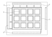
도 1 및 도 2는 종래의 유기전계 발광소자의 일례를 나타낸 것으로, 유기전계 발광소자(OLED)는 기판(1)과, 상기 기판(1)의 일면에 도포되는 배선전극(2) 및 보조전극(3), 상기 배선전극(2) 및 보조전극(3)을 덮도록 도포되는 양극전극(anode)인 투명전극(4), 상기 투명전극(4) 상에 차례로 도포되는 절연막(5)과 유기발광층(6) 및 캐소드전극(7), 상기 전극과 유기물들이 공기 중의 수분이나 산소, NOx 등과 접촉하지 않도록 상기 전극 및 유기물이 형성된 면을 밀폐하는 봉지용 커버(8) 및 실링재(9) 등으로 구성될 수 있다.1 and 2 illustrate an example of a conventional organic light emitting diode, and the organic light emitting diode OLED includes a
상기 유기전계 발광소자는 배선전극(2)과 보조전극(3)이 먼저 형성되고, 그 위에 투명전극(4)이 도포된 구조로 이루어져 있지만, 이와 다르게 투명전극(4)이 먼저 기판(1) 상에 도포되고, 상기 투명전극(4) 위에 배선전극(2)과 보조전극(3)이 형성될 수도 있다. The organic electroluminescent device has a structure in which the
한편, 상기와 같이 구성된 종래의 유기전계 발광소자는 상기 보조전극(3)의 테두리 부분과 기판(1) 면이 대략 직각으로 단차진 구조로 이루어져 있기 때문에 보조전극(3)의 바로 위에 유기발광층(6)을 형성할 경우 유기발광층(6)의 두께가 얇아져 전계가 집중되고 누설(leakage) 및 열화의 원인되는 문제가 발생하게 된다. On the other hand, the conventional organic EL device configured as described above has an organic light emitting layer directly above the
이에 따라 종래에는 보조전극(3)의 상측에 절연막(5)을 형성하되, 절연막(5)의 테두리 부분이 기판(1) 면에 대해 소정 각도 이하로 경사지게 형성하여 상부에 형성되는 유기발광층(6)의 두께 감소를 방지하고 있다. Accordingly, the organic
하지만, 상기와 같이 보조전극(3)의 상측에 보조전극(3)보다 넓은 영역으로 절연막(5)이 형성되면, 비발광영역인 절연막(5)으로 인하여 개구율이 감소하는 문제가 발생하게 된다. However, when the
본 발명은 상기와 같은 문제를 해결하기 위한 것으로, 본 발명의 목적은 보조전극의 상부에 절연막과 같은 비발광영역을 형성하지 않도록 하여 개구율을 향상시킴과 더불어 간단하고 용이하게 제조할 수 있는 유기전계 발광소자 및 그 제조방법을 제공함에 있다.The present invention is to solve the above problems, an object of the present invention is to improve the aperture ratio by not forming a non-light emitting region such as an insulating film on the auxiliary electrode, an organic field that can be easily and easily manufactured A light emitting device and a method of manufacturing the same are provided.
상기와 같은 목적을 달성하기 위한 본 발명은, 기판과; 상기 기판의 일면에 형성되어 주전원을 공급하는 배선전극과; 상기 기판의 일면에 일정 패턴으로 형성되며, 양측 가장자리 부분이 기판 면에 대해 일정 각도로 경사진 경사면을 이루는 보조전극과; 상기 배선전극 및 보조전극 중 적어도 일부를 덮도록 도포되는 제1전극과; 상기 제1전극의 상에 도포되는 유기물로 이루어진 유기발광층과; 상기 유기발광층 상에 형성되는 제2전극을 포함하는 것을 특징으로 하는 유기전계 발광소자를 제공한다. The present invention for achieving the above object, the substrate; A wiring electrode formed on one surface of the substrate to supply main power; An auxiliary electrode formed on one surface of the substrate in a predetermined pattern and having an inclined surface inclined at an angle with respect to the substrate surface at both edges thereof; A first electrode applied to cover at least a portion of the wiring electrode and the auxiliary electrode; An organic light emitting layer made of an organic material coated on the first electrode; It provides an organic electroluminescent device comprising a second electrode formed on the organic light emitting layer.
본 발명의 다른 한 형태에 따르면, 상기 유기전계 발광소자의 제조방법으로서 (a) 보조전극 패턴과 대응하는 패턴의 관통공이 형성되어 있는 섀도우 마스크를 기판의 일면에 연접하거나 일정 거리 이격되게 배치하는 단계와; (b) 진공증착 또는 스퍼터링 공정에 의해 기판의 일면에 보조전극을 형성하는 단계와; (c) 상기 보조전극 및 기판의 일면에 제1전극을 형성하는 단계와; (d) 상기 제1전극 상에 유기물로 이루어진 유기발광층을 형성하는 단계와; (e) 상기 유기발광층 상에 제2전극을 형성하는 단계를 포함하는 것을 특징으로 하는 유기전계 발광소자의 제조방법이 제공된다.According to another aspect of the present invention, a method of manufacturing the organic light emitting device includes (a) disposing a shadow mask having a through hole of a pattern corresponding to the auxiliary electrode pattern in contact with one surface of the substrate or spaced a predetermined distance apart from each other. Wow; (b) forming an auxiliary electrode on one surface of the substrate by vacuum deposition or sputtering; (c) forming a first electrode on one surface of the auxiliary electrode and the substrate; (d) forming an organic light emitting layer formed of an organic material on the first electrode; (e) providing a method of manufacturing an organic light emitting device, comprising forming a second electrode on the organic light emitting layer.
이와 같은 본 발명에 따르면, 섀도우 마스크를 사용한 진공증착 또는 스퍼터링에 의해 보조전극의 양측 가장자리 부분에 기판 면에 대해 소정 각도 이하로 경사진 경사면이 형성된다. 따라서, 기존의 절연막을 형성하지 않고 유기발광층의 두께를 증대시킬 수 있으며, 절연막으로 인한 개구율 감소를 방지할 수 있는 효과가 있다. According to the present invention, an inclined surface inclined to a predetermined angle or less with respect to the substrate surface is formed on both edge portions of the auxiliary electrode by vacuum deposition or sputtering using a shadow mask. Therefore, the thickness of the organic light emitting layer can be increased without forming an existing insulating film, and the reduction of the aperture ratio due to the insulating film can be prevented.
또한, 포토리소그래피와 같은 복잡한 공정을 수행하지 않고 섀도우 마스크를 이용한 진공증착 또는 스퍼터링에 의해 보조전극을 형성할 수 있으므로 제조 공정이 대폭 단순화되고, 생산성을 향상시킬 수 있는 이점도 있다. In addition, since the auxiliary electrode may be formed by vacuum deposition or sputtering using a shadow mask without performing a complicated process such as photolithography, the manufacturing process may be greatly simplified, and the productivity may be improved.
도 1은 종래의 유기전계 발광소자의 구조를 개략적으로 나타낸 종단면도이다.
도 2는 도 1의 유기전계 발광소자의 일부 구성을 생략하여 나타낸 평면도이다.
도 3은 본 발명의 일 실시예에 따른 유기전계 발광소자의 구조를 개략적으로 나타낸 종단면도이다.
도 4는 도 3의 유기전계 발광소자의 일부 구성을 생략하여 나타낸 평면도이다.
도 5는 도 3의 유기전계 발광소자의 배선전극 및 보조전극을 형성하기 위한 섀도우 마스크의 형태를 나타낸 평면도이다. 1 is a longitudinal sectional view schematically showing a structure of a conventional organic light emitting device.
FIG. 2 is a plan view omitting some components of the organic light emitting diode of FIG. 1.
3 is a longitudinal sectional view schematically showing the structure of an organic light emitting display device according to an embodiment of the present invention.
FIG. 4 is a plan view omitting some components of the organic light emitting diode of FIG. 3.
FIG. 5 is a plan view illustrating a shape of a shadow mask for forming the wiring electrode and the auxiliary electrode of the organic light emitting diode of FIG. 3.
이하 첨부된 도면을 참조하여 본 발명에 따른 유기전계 발광소자 및 그 제조방법의 바람직한 실시예를 상세히 설명한다. Hereinafter, exemplary embodiments of an organic light emitting diode and a method of manufacturing the same according to the present invention will be described in detail with reference to the accompanying drawings.
도 3 및 도 4는 본 발명의 바람직한 실시예에 따른 유기전계 발광소자의 구조를 나타낸 것으로, 이 실시예의 유기전계 발광소자(OLED)는 기판(10)과, 상기 기판(10)의 상면에 소정의 패턴으로 도포되며 외부 전원과 연결되어 주전원을 공급하는 배선전극(20) 및 상기 배선전극(20)의 내측에 격자형태로 연결되는 보조전극(30), 상기 배선전극(20) 및 보조전극(30) 중 적어도 일부를 덮도록 도포되는 제1전극과(40), 상기 제1전극(40) 상에 차례로 도포되는 유기발광층(60) 및 제2전극(70), 상기 전극과 유기물들이 공기 중의 수분이나 산소, NOx 등과 접촉하지 않도록 상기 전극 및 유기물이 형성된 면을 밀폐하는 봉지용 커버(80) 및 실링재(90) 등을 포함한 구성으로 이루어진다. 3 and 4 illustrate the structure of an organic light emitting diode according to a preferred embodiment of the present invention. The organic light emitting diode OLED of this embodiment has a
이 실시예에서 상기 제1전극(40)은 양극전극(anode)인 ITO 투명전극이고, 제2전극(70)은 캐소드전극(cathode)이나, 이와 반대로 될 수도 있다. In this embodiment, the
상기 배선전극(20)은 제1전극(40)과 제2전극(70) 각각에 전원을 공급하기 위한 것으로서 기판(10)의 네 테두리 부분을 따라 형성되며, 보조전극(30)은 기판(10)을 가로 방향과 세로 방향으로 가로지르면서 서로 교차되어 격자형(grid) 패턴으로 형성된다. The
상기 보조전극(30)은 양측 가장자리 부분이 기판(10)의 면에 대해 일정 각도 이하로, 바람직하기로는 10~30도의 각도로 경사진 경사면(31)으로 형성된다. 상기 경사면(31)의 각도가 30도보다 크게 되면 두께가 너무 얇아지게 되고, 10도보다 작아지게 되면 보조전극(30)이 지나치게 넓어져 유기전계 발광소자 전체의 빛 투과율이 낮아지게 되는 문제가 있다. 이와 같이 보조전극(30)의 양측 가장자리가 일정 각도 이하의 경사면(31)으로 형성되면 보조전극(30)의 상부에 형성되는 유기발광층(60)의 막두께를 증가시킬 수 있으므로 기존의 절연막을 형성할 필요가 없게 된다. The
상기 배선전극(20) 및 보조전극(30)은 알루미늄(Al), 은(Ag), 크롬(Cr), 알루미늄-네오디뮴(AlNd), 알루미늄/몰리브덴(Al/Mo) 등의 저저항 금속을 사용하여 만들어질 수 있으나, 이외에도 다양한 임의의 금속을 사용하여 만들어질 수 있다. 상기 배선전극(20) 및 보조전극(30)은 도 5에 도시된 것과 같은 섀도우 마스크(100)를 이용하여 물리증착법(PVD: physical vapor deposition), 화학증착법(CVD: chemical vapor deposition), 또는 스퍼터링(sputtering) 방식으로 형성된다. The
즉, 배선전극(20) 및 보조전극(30)과 대응하는 패턴의 관통공(101)을 갖는 섀도우 마스크(100)를 상기 기판(10)의 상면과 연접하거나 소정 거리 이격되게 배치하고, 진공증착 또는 열증착이나 evaporation 공정으로 배선전극(20) 및 보조전극(30)을 형성한다. 이 때, 상기 섀도우 마스크(100)의 보조전극(30)에 대응하는 관통공(101)의 양측 가장자리 부분은 기판(10) 면에 대해 소정 각도 경사지게 형성되어 보조전극(30)의 양측 가장자리에 경사면(31)이 형성된다. That is, the
상기 보조전극(30)의 경사면(31)의 각도는 상기 섀도우 마스크(100)의 관통공(101)의 양측 가장자리 내주면의 경사각을 조정하거나 섀도우 마스크(100)와 기판(10) 면 간의 거리를 조정함으로써 조정될 수 있다. 상기 섀도우 마스크(100)와 기판(10) 면 간의 간격이 증가할수록 경사도가 낮아지게 된다.The angle of the
또한, 상기 보조전극(30)을 형성하는 과정에서 보조전극(30)의 경사면(31)의 표면상태(roughness)가 일정치 않을 경우, 보조전극(30) 형성 후 고온의 어닐링(annealing) 공정으로 국부적인 히트리플로우(heat reflow)를 시키거나, 표면을 플라즈마 등으로 처리하여 경사면(31)의 표면을 매끄럽고 균일하게 개선할 수 있다. In addition, when the surface state (roughness) of the
한편, 상기 배선전극(20)과 보조전극(30)을 기판(10) 면에 형성한 이후에는 상기 배선전극(20)과 보조전극(30) 상측을 덮도록 제1전극인 투명전극(40)이 도포되고, 상기 투명전극(40) 상에 유기물로 이루어진 유기발광층(60)이 도포되며, 유기발광층(60) 상에 제2전극인 캐소드전극(70)이 도포되는 방식으로 제조된다. Meanwhile, after the
상기 투명전극(40) 및 유기발광층(60)이 도포될 때, 상기 보조전극(30)의 양측 가장자리 부분은 소정 각도(예를 들어 30도 이하)로 경사진 경사면(31)을 이루고 있기 때문에 기존의 절연막을 형성하지 않아도 상기 유기발광층(60)의 두께 감소가 방지될 수 있게 된다. 또한, 기존의 절연막에 의한 개구율 감소를 방지할 수 있으며, 유기전계 발광소자의 전체 제조 공정도 단순화되어 생산성을 향상시킬 수 있는 이점이 있다. When the
이상에서는 본 발명에 대한 기술사상을 첨부 도면과 함께 서술하였지만 이는 본 발명의 바람직한 실시예를 예시적으로 설명한 것이지 본 발명을 한정하는 것은 아니다. 또한 본 발명이 속하는 기술 분야에서 통상의 지식을 가진 이라면 누구나 본 발명의 기술적 사상의 범주를 이탈하지 않는 범위 내에서 다양한 변형 및 모방이 가능함은 명백한 사실이다.While the present invention has been described in connection with what is presently considered to be the most practical and preferred embodiment, it is to be understood that the invention is not limited to the disclosed embodiments. It will be apparent to those skilled in the art that various modifications and variations can be made in the present invention without departing from the scope of the present invention.
10 : 기판 20 : 배선전극
30 : 보조전극 31 : 경사면
40 : 양극전극(제1전극) 60 : 유기발광층
70 : 캐소드전극(제2전극) 100 : 섀도우 마스크
101 : 관통공10: substrate 20: wiring electrode
30: auxiliary electrode 31: inclined surface
40: anode electrode (first electrode) 60: organic light emitting layer
70: cathode electrode (second electrode) 100: shadow mask
101: through hole
Claims (6)
상기 기판(10)의 일면에 형성되어 주전원을 공급하는 배선전극(20)과;
상기 기판(10)의 일면에 일정 패턴으로 형성되며, 양측 가장자리 부분이 기판(10) 면에 대해 일정 각도로 경사진 경사면(31)을 이루는 보조전극(30)과;
상기 배선전극(2) 및 보조전극(3) 중 적어도 일부를 덮도록 도포되는 제1전극과;
상기 제1전극의 상에 도포되는 유기물로 이루어진 유기발광층(60)과;
상기 유기발광층(60) 상에 형성되는 제2전극(70)을 포함하는 것을 특징으로 하는 유기전계 발광소자.A substrate (10);
A wiring electrode 20 formed on one surface of the substrate 10 to supply main power;
An auxiliary electrode 30 formed on one surface of the substrate 10 in a predetermined pattern and having an inclined surface 31 inclined at an angle with respect to the surface of the substrate 10 at both edges thereof;
A first electrode applied to cover at least a portion of the wiring electrode 2 and the auxiliary electrode 3;
An organic light emitting layer 60 formed of an organic material coated on the first electrode;
An organic light emitting device, characterized in that it comprises a second electrode (70) formed on the organic light emitting layer (60).
(b) 물리증착 또는 화학증착 공정에 의해 기판(10)의 일면에 보조전극(30)을 형성하는 단계와;
(c) 상기 보조전극(30) 및 기판(10)의 일면에 제1전극(40)을 형성하는 단계와;
(d) 상기 제1전극(40) 상에 유기물로 이루어진 유기발광층(60)을 형성하는 단계와;
(e) 상기 유기발광층(60) 상에 제2전극(70)을 형성하는 단계를 포함하는 것을 특징으로 하는 제1항 또는 제2항의 유기전계 발광소자의 제조방법.(a) disposing a shadow mask 100 having a through hole 101 having a pattern corresponding to the pattern of the auxiliary electrode 30 in contact with one surface of the substrate 10 or spaced at a predetermined distance;
(b) forming an auxiliary electrode 30 on one surface of the substrate 10 by physical vapor deposition or chemical vapor deposition;
(c) forming a first electrode 40 on one surface of the auxiliary electrode 30 and the substrate 10;
(d) forming an organic light emitting layer 60 made of an organic material on the first electrode 40;
(e) forming a second electrode (70) on the organic light emitting layer (60).
The organic field of claim 3, wherein the inclination angle of the inclined surface 31 of the auxiliary electrode 30 is adjusted by adjusting the distance between the shadow mask 100 and the substrate 10 in step (b). Method of manufacturing a light emitting device.
Priority Applications (1)
| Application Number | Priority Date | Filing Date | Title |
|---|---|---|---|
| KR1020110096957A KR20130033093A (en) | 2011-09-26 | 2011-09-26 | Organic light emitting diode(oled) and method for manufacturing the same |
Applications Claiming Priority (1)
| Application Number | Priority Date | Filing Date | Title |
|---|---|---|---|
| KR1020110096957A KR20130033093A (en) | 2011-09-26 | 2011-09-26 | Organic light emitting diode(oled) and method for manufacturing the same |
Publications (1)
| Publication Number | Publication Date |
|---|---|
| KR20130033093A true KR20130033093A (en) | 2013-04-03 |
Family
ID=48435672
Family Applications (1)
| Application Number | Title | Priority Date | Filing Date |
|---|---|---|---|
| KR1020110096957A Ceased KR20130033093A (en) | 2011-09-26 | 2011-09-26 | Organic light emitting diode(oled) and method for manufacturing the same |
Country Status (1)
| Country | Link |
|---|---|
| KR (1) | KR20130033093A (en) |
Cited By (3)
| Publication number | Priority date | Publication date | Assignee | Title |
|---|---|---|---|---|
| WO2015009121A1 (en) * | 2013-07-19 | 2015-01-22 | 주식회사 엘지화학 | Electrode laminate and organic light emitting element |
| WO2018235594A1 (en) * | 2017-06-22 | 2018-12-27 | 住友化学株式会社 | Method for producing transparent electrode and method for producing electronic device |
| CN109841750A (en) * | 2017-11-28 | 2019-06-04 | 乐金显示有限公司 | OLED lighting apparatus |
-
2011
- 2011-09-26 KR KR1020110096957A patent/KR20130033093A/en not_active Ceased
Cited By (13)
| Publication number | Priority date | Publication date | Assignee | Title |
|---|---|---|---|---|
| US10381590B2 (en) | 2013-07-19 | 2019-08-13 | Lg Display Co., Ltd. | Electrode laminate and organic light emitting device element |
| CN105637667A (en) * | 2013-07-19 | 2016-06-01 | 株式会社Lg化学 | Electrode laminate and organic light emitting element |
| US20160172619A1 (en) * | 2013-07-19 | 2016-06-16 | Lg Chem, Ltd. | Electrode laminate and organic light emitting device element |
| JP2016524304A (en) * | 2013-07-19 | 2016-08-12 | エルジー・ケム・リミテッド | Electrode laminate and organic light emitting device |
| TWI562427B (en) * | 2013-07-19 | 2016-12-11 | Lg Display Co Ltd | Electrode laminate and organic light emitting device |
| CN105637667B (en) * | 2013-07-19 | 2018-08-10 | 乐金显示有限公司 | Electrode layered product and organic illuminating element |
| WO2015009121A1 (en) * | 2013-07-19 | 2015-01-22 | 주식회사 엘지화학 | Electrode laminate and organic light emitting element |
| US20190305245A1 (en) * | 2013-07-19 | 2019-10-03 | Lg Display Co., Ltd | Electrode laminate and organic light emitting device element |
| US10749132B2 (en) | 2013-07-19 | 2020-08-18 | Lg Display Co., Ltd. | Electrode laminate and organic light emitting device element |
| WO2018235594A1 (en) * | 2017-06-22 | 2018-12-27 | 住友化学株式会社 | Method for producing transparent electrode and method for producing electronic device |
| JP2019008942A (en) * | 2017-06-22 | 2019-01-17 | 住友化学株式会社 | Manufacturing method of transparent electrode and manufacturing method of electronic device |
| CN109841750A (en) * | 2017-11-28 | 2019-06-04 | 乐金显示有限公司 | OLED lighting apparatus |
| US10910585B2 (en) | 2017-11-28 | 2021-02-02 | Lg Display Co., Ltd. | OLED lighting apparatus having a double layered electrode |
Similar Documents
| Publication | Publication Date | Title |
|---|---|---|
| CN109103215B (en) | Organic light emitting diode display panel, manufacturing method thereof and display device | |
| US9881985B2 (en) | OLED device, AMOLED display device and method for manufacturing same | |
| KR102076034B1 (en) | Organic light emitting diode display and manufacturing method thereof | |
| CN104701351B (en) | Oled substrate and preparation method thereof, OLED display panel and electronic equipment | |
| WO2018113019A1 (en) | Oled display panel and manufacturing method therefor | |
| WO2018113018A1 (en) | Oled display panel and manufacturing method therefor | |
| US20200194732A1 (en) | Oled display substrate and method for preparing the same, and display device | |
| US9705104B2 (en) | OLED display substrate and manufacture method thereof | |
| US10553812B2 (en) | Organic electroluminescent device and manufacturing method thereof, display device | |
| WO2019085045A1 (en) | Preparation method for oled anode and preparation method for oled display device | |
| JP5557653B2 (en) | Thin film deposition apparatus and organic light emitting display device manufacturing method using the same | |
| US10270054B2 (en) | Organic light-emitting diode components including an insulating layer and an auxiliary electrode layer positioned above the insulating layer, manufacturing methods for organic light-emitting diode components, display panels including organic light-emitting diode components, and display devices | |
| US20210210589A1 (en) | Display Substrate, Manufacturing Method Thereof and Display Device | |
| US20140191200A1 (en) | Apparatus and Method for Making OLED Lighting Device | |
| TW201324888A (en) | The organic light-emitting diode and display comprising the same | |
| US20190173009A1 (en) | Organic electroluminescent device and preparation method, evaporation device | |
| KR20130033093A (en) | Organic light emitting diode(oled) and method for manufacturing the same | |
| KR101192003B1 (en) | Shadow mask for manufacturing oled, apparatus and method for manufacturing oled using the same | |
| JP6938754B2 (en) | Light emitting device | |
| KR20130033100A (en) | Organic light emitting diode(oled) | |
| KR101920759B1 (en) | Method of fabricating organic light emitting display device | |
| KR20130005853A (en) | Organic light emitting diodes | |
| KR100739645B1 (en) | Organic light emitting display | |
| JP6817857B2 (en) | Light emitting device | |
| KR100739579B1 (en) | OLED display and manufacturing method thereof |
Legal Events
| Date | Code | Title | Description |
|---|---|---|---|
| PA0109 | Patent application |
St.27 status event code: A-0-1-A10-A12-nap-PA0109 |
|
| PG1501 | Laying open of application |
St.27 status event code: A-1-1-Q10-Q12-nap-PG1501 |
|
| R17-X000 | Change to representative recorded |
St.27 status event code: A-3-3-R10-R17-oth-X000 |
|
| PN2301 | Change of applicant |
St.27 status event code: A-3-3-R10-R13-asn-PN2301 St.27 status event code: A-3-3-R10-R11-asn-PN2301 |
|
| R18-X000 | Changes to party contact information recorded |
St.27 status event code: A-3-3-R10-R18-oth-X000 |
|
| A201 | Request for examination | ||
| PA0201 | Request for examination |
St.27 status event code: A-1-2-D10-D11-exm-PA0201 |
|
| R18-X000 | Changes to party contact information recorded |
St.27 status event code: A-3-3-R10-R18-oth-X000 |
|
| D13-X000 | Search requested |
St.27 status event code: A-1-2-D10-D13-srh-X000 |
|
| D14-X000 | Search report completed |
St.27 status event code: A-1-2-D10-D14-srh-X000 |
|
| E902 | Notification of reason for refusal | ||
| PE0902 | Notice of grounds for rejection |
St.27 status event code: A-1-2-D10-D21-exm-PE0902 |
|
| PE0601 | Decision on rejection of patent |
St.27 status event code: N-2-6-B10-B15-exm-PE0601 |
|
| P22-X000 | Classification modified |
St.27 status event code: A-2-2-P10-P22-nap-X000 |
|
| P22-X000 | Classification modified |
St.27 status event code: A-2-2-P10-P22-nap-X000 |
|
| P22-X000 | Classification modified |
St.27 status event code: A-2-2-P10-P22-nap-X000 |
|
| P22-X000 | Classification modified |
St.27 status event code: A-2-2-P10-P22-nap-X000 |