KR20130008302A - Method of controlling read voltage in flash memory device and method of reading data using the same - Google Patents
Method of controlling read voltage in flash memory device and method of reading data using the same Download PDFInfo
- Publication number
- KR20130008302A KR20130008302A KR1020110068972A KR20110068972A KR20130008302A KR 20130008302 A KR20130008302 A KR 20130008302A KR 1020110068972 A KR1020110068972 A KR 1020110068972A KR 20110068972 A KR20110068972 A KR 20110068972A KR 20130008302 A KR20130008302 A KR 20130008302A
- Authority
- KR
- South Korea
- Prior art keywords
- read
- count information
- page
- data
- flash memory
- Prior art date
- Legal status (The legal status is an assumption and is not a legal conclusion. Google has not performed a legal analysis and makes no representation as to the accuracy of the status listed.)
- Granted
Links
Images


Classifications
-
- G—PHYSICS
- G11—INFORMATION STORAGE
- G11C—STATIC STORES
- G11C16/00—Erasable programmable read-only memories
- G11C16/02—Erasable programmable read-only memories electrically programmable
- G11C16/06—Auxiliary circuits, e.g. for writing into memory
- G11C16/26—Sensing or reading circuits; Data output circuits
-
- G—PHYSICS
- G11—INFORMATION STORAGE
- G11C—STATIC STORES
- G11C16/00—Erasable programmable read-only memories
- G11C16/02—Erasable programmable read-only memories electrically programmable
- G11C16/06—Auxiliary circuits, e.g. for writing into memory
- G11C16/10—Programming or data input circuits
-
- G—PHYSICS
- G11—INFORMATION STORAGE
- G11C—STATIC STORES
- G11C16/00—Erasable programmable read-only memories
- G11C16/02—Erasable programmable read-only memories electrically programmable
- G11C16/06—Auxiliary circuits, e.g. for writing into memory
- G11C16/30—Power supply circuits
-
- G—PHYSICS
- G11—INFORMATION STORAGE
- G11C—STATIC STORES
- G11C11/00—Digital stores characterised by the use of particular electric or magnetic storage elements; Storage elements therefor
- G11C11/56—Digital stores characterised by the use of particular electric or magnetic storage elements; Storage elements therefor using storage elements with more than two stable states represented by steps, e.g. of voltage, current, phase, frequency
- G11C11/5621—Digital stores characterised by the use of particular electric or magnetic storage elements; Storage elements therefor using storage elements with more than two stable states represented by steps, e.g. of voltage, current, phase, frequency using charge storage in a floating gate
- G11C11/5628—Programming or writing circuits; Data input circuits
-
- G—PHYSICS
- G11—INFORMATION STORAGE
- G11C—STATIC STORES
- G11C11/00—Digital stores characterised by the use of particular electric or magnetic storage elements; Storage elements therefor
- G11C11/56—Digital stores characterised by the use of particular electric or magnetic storage elements; Storage elements therefor using storage elements with more than two stable states represented by steps, e.g. of voltage, current, phase, frequency
- G11C11/5621—Digital stores characterised by the use of particular electric or magnetic storage elements; Storage elements therefor using storage elements with more than two stable states represented by steps, e.g. of voltage, current, phase, frequency using charge storage in a floating gate
- G11C11/5642—Sensing or reading circuits; Data output circuits
Landscapes
- Read Only Memory (AREA)
Abstract
본 발명에 따른 플래시 메모리 장치의 리드 전압 조절 방법이 제공된다. 상기 리드 전압 조절 방법에 따르면, 적어도 하나의 페이지를 갖는 플래시 메모리 셀들의 프로그램 시에, 상기 플래시 메모리 셀들의 제1 페이지에 프로그램되는 데이터의 비트들 중에서 제1 논리 값을 갖는 비트들의 개수인 제1 프로그램 카운트 정보가 저장된다. 리드 전압들을 이용한 상기 플래시 메모리 셀들의 리드 시에, 상기 플래시 메모리 셀들의 상기 제1 페이지로부터 리드되는 데이터의 비트들 중에서 상기 제1 논리 값을 갖는 비트들의 개수를 계수하여 제1 리드 카운트 정보가 획득된다. 상기 제1 프로그램 카운트 정보와 상기 제1 리드 카운트 정보의 차이를 기초로 상기 리드 전압들의 전압 레벨들이 조절된다.A read voltage adjusting method of a flash memory device according to the present invention is provided. According to the read voltage adjusting method, when programming flash memory cells having at least one page, a first number of bits having a first logical value among bits of data programmed in a first page of the flash memory cells. Program count information is stored. When reading the flash memory cells using read voltages, first read count information is obtained by counting the number of bits having the first logic value among bits of data read from the first page of the flash memory cells. do. The voltage levels of the read voltages are adjusted based on the difference between the first program count information and the first read count information.
Description
본 발명은 플래시 메모리 기술에 관한 것으로, 보다 상세하게는 플래시 메모리 장치에 프로그램된 데이터의 상태를 기초로 리드 전압의 전압 레벨을 조절하는 방법, 및 이를 이용한 데이터 리드 방법에 관한 것이다.The present invention relates to a flash memory technology, and more particularly, to a method of adjusting a voltage level of a read voltage based on a state of data programmed in a flash memory device, and a data read method using the same.
일반적으로 플래시 메모리는 하나의 메모리 셀에 프로그램되는 데이터 비트 수에 따라 싱글 레벨 셀(Single-Level Cell, SLC)과 멀티 레벨 셀(Multi-Level Cell, MLC)로 나눌 수 있다. 싱글 레벨 셀은 2가지 셀 산포를 가지며, M-비트(M은 2이상의 정수) 멀티 레벨 셀은 2M가지의 셀 산포를 갖는다. 그러나, 여러 원인들에 의하여 프로그램된 메모리 셀의 산포가 변할 수 있으며, 그에 따라 메모리 셀에 프로그램한 데이터와 메모리 셀로부터 리드된 데이터가 달라지는 문제가 있다.In general, a flash memory may be divided into a single-level cell (SLC) and a multi-level cell (MLC) according to the number of data bits programmed in one memory cell. Single-level cells have two cell spreads, and M-bit (M is an integer of two or more) multi-level cells have 2M cell spreads. However, the distribution of the programmed memory cell may change due to various causes, and thus there is a problem in that data programmed in the memory cell and data read from the memory cell are different.
따라서, 본 발명이 이루고자 하는 기술적 과제는 데이터 신뢰성을 향상시키고 데이터 출력 속도를 줄일 수 있는 플래시 메모리 장치의 리드 전압 조절 방법을 제공하는 것이다. Accordingly, an object of the present invention is to provide a read voltage adjusting method of a flash memory device capable of improving data reliability and reducing data output speed.
또한, 본 발명이 이루고자 하는 기술적 과제는 데이터 신뢰성을 향상시키고 데이터 출력 속도를 줄일 수 있는 플래시 메모리 장치의 데이터 리드 방법을 제공하는 것이다.Another object of the present invention is to provide a data read method of a flash memory device capable of improving data reliability and reducing data output speed.
상기 기술적 과제를 달성하기 위한 본 발명의 일 실시예에 따른 플래시 메모리 장치의 리드 전압 조절 방법이 제공된다. 상기 플래시 메모리 장치의 리드 전압 조절 방법에 따르면, 적어도 하나의 페이지를 갖는 플래시 메모리 셀들의 프로그램 시에, 상기 플래시 메모리 셀들의 제1 페이지에 프로그램되는 데이터의 비트들 중에서 제1 논리 값을 갖는 비트들의 개수인 제1 프로그램 카운트 정보가 저장된다. 리드 전압들을 이용한 상기 플래시 메모리 셀들의 리드 시에, 상기 플래시 메모리 셀들의 상기 제1 페이지로부터 리드되는 데이터의 비트들 중에서 상기 제1 논리 값을 갖는 비트들의 개수를 계수하여 제1 리드 카운트 정보가 획득된다. 상기 제1 프로그램 카운트 정보와 상기 제1 리드 카운트 정보의 차이를 기초로 상기 리드 전압들의 전압 레벨들이 조절된다.According to an aspect of the present invention, there is provided a method of controlling read voltage of a flash memory device. According to the read voltage adjusting method of the flash memory device, when programming flash memory cells having at least one page, the bits having the first logical value among the bits of data programmed in the first page of the flash memory cells. The first program count information, which is a count, is stored. When reading the flash memory cells using read voltages, first read count information is obtained by counting the number of bits having the first logic value among bits of data read from the first page of the flash memory cells. do. The voltage levels of the read voltages are adjusted based on the difference between the first program count information and the first read count information.
상기 플래시 메모리 장치의 리드 전압 조절 방법의 일 예에 따르면, 상기 리드 전압들의 전압 레벨들을 조절하는 단계에서, 상기 제1 프로그램 카운트 정보와 상기 제1 리드 카운트 정보의 차이에 대응하는 상기 리드 전압들의 전압 레벨 보상 값들이 상기 리드 전압들에 적용될 수 있다.According to an example of a read voltage adjusting method of the flash memory device, in the adjusting of the voltage levels of the read voltages, the voltage of the read voltages corresponding to the difference between the first program count information and the first read count information. Level compensation values may be applied to the read voltages.
상기 플래시 메모리 장치의 리드 전압 조절 방법의 다른 예에 따르면, 상기 리드 전압들의 전압 레벨들을 조절하는 단계에서, 상기 제1 프로그램 카운트 정보와 상기 제1 리드 카운트 정보의 차이에 비례하여 상기 리드 전압들의 전압 레벨들이 상승되거나 하강될 수 있다. According to another example of a read voltage adjusting method of the flash memory device, in the adjusting of the voltage levels of the read voltages, the voltage of the read voltages in proportion to the difference between the first program count information and the first read count information. Levels can be raised or lowered.
상기 플래시 메모리 장치의 리드 전압 조절 방법의 또 다른 예에 따르면, 상기 플래시 메모리 셀들의 프로그램 시에, 상기 플래시 메모리 셀들의 제2 페이지에 프로그램되는 데이터의 비트들이 상기 제1 논리 값을 갖는 개수가 제2 프로그램 카운트 정보로서 저장될 수 있다. 상기 플래시 메모리 셀들의 리드 시에, 상기 플래시 메모리 셀들의 상기 제2 페이지로부터 리드되는 데이터의 비트들이 상기 제1 논리 값을 갖는 개수가 계수되어 제2 리드 카운트 정보가 획득될 수 있다. 상기 리드 전압들의 전압 레벨들을 조절하는 단계에서, 상기 리드 전압들의 전압 레벨들은 상기 제1 프로그램 카운트 정보와 상기 제1 리드 카운트 정보의 차이, 및 상기 제2 프로그램 카운트 정보와 상기 제2 리드 카운트 정보의 차이를 기초로 조절될 수 있다.According to another example of the method of adjusting the read voltage of the flash memory device, when the flash memory cells are programmed, the number of bits of data programmed in the second page of the flash memory cells having the first logic value is equal to the first. 2 can be stored as program count information. When reading the flash memory cells, the number of bits of data read from the second page of the flash memory cells having the first logic value may be counted to obtain second read count information. In adjusting the voltage levels of the read voltages, the voltage levels of the read voltages are different from the first program count information and the first read count information, and the second program count information and the second read count information. It can be adjusted based on the difference.
상기 플래시 메모리 장치의 리드 전압 조절 방법의 또 다른 예에 따르면, 상기 리드 전압들의 전압 레벨들을 조절하는 단계에서, 상기 제1 프로그램 카운트 정보와 상기 제1 리드 카운트 정보의 차이, 및 상기 제2 프로그램 카운트 정보와 상기 제2 리드 카운트 정보의 차이를 기초로 오류 모드가 결정될 수 있다. 상기 결정된 오류 모드에 따라서, 상기 제1 프로그램 카운트 정보와 상기 제1 리드 카운트 정보의 차이, 및 상기 제2 프로그램 카운트 정보와 상기 제2 리드 카운트 정보의 차이에 대응하는 상기 리드 전압들의 전압 레벨 보상 값들이 리드될 수 있다. 상기 리드 전압들의 전압 레벨 보상 값들이 상기 리드 전압들에 각각 적용될 수 있다.According to another example of a read voltage adjusting method of the flash memory device, in the adjusting of the voltage levels of the read voltages, a difference between the first program count information and the first read count information, and the second program count An error mode may be determined based on a difference between the information and the second read count information. According to the determined error mode, a voltage level compensation value of the read voltages corresponding to a difference between the first program count information and the first read count information and a difference between the second program count information and the second read count information. Can be lead. Voltage level compensation values of the read voltages may be applied to the read voltages, respectively.
상기 플래시 메모리 장치의 리드 전압 조절 방법의 또 다른 예에 따르면, 상기 리드 전압들의 전압 레벨들을 조절하는 단계에서, 상기 제1 프로그램 카운트 정보와 상기 제1 리드 카운트 정보의 차이가 소정의 범위 이내인 경우, 상기 제2 프로그램 카운트 정보와 상기 제2 리드 카운트 정보의 차이를 기초로 상기 리드 전압들 중 일부의 전압 레벨들이 낮춰지거나 높여질 수 있다. According to another example of the read voltage adjusting method of the flash memory device, when the voltage levels of the read voltages are adjusted, the difference between the first program count information and the first read count information is within a predetermined range. The voltage levels of some of the read voltages may be lowered or raised based on the difference between the second program count information and the second read count information.
상기 플래시 메모리 장치의 리드 전압 조절 방법의 또 다른 예에 따르면, 수신된 데이터가 랜덤화(randomization)되어 상기 플래시 메모리 셀들에 프로그램될 수 있다. 상기 플래시 메모리 셀들로부터 리드되는 데이터가 디랜덤화(derandomization)될 수 있다. According to another example of the read voltage adjusting method of the flash memory device, the received data may be randomized and programmed in the flash memory cells. Data read from the flash memory cells may be derandomized.
상기 플래시 메모리 장치의 리드 전압 조절 방법의 또 다른 예에 따르면, 상기 제1 프로그램 카운트 정보가 랜덤화되어 상기 플래시 메모리 셀들의 스페어 영역에 저장될 수 있다. 상기 스페어 영역에 저장된 랜덤화된 상기 제1 프로그램 카운트 정보는 디랜덤화되어 리드될 수 있다.According to another example of the read voltage adjusting method of the flash memory device, the first program count information may be randomized and stored in a spare area of the flash memory cells. The randomized first program count information stored in the spare area may be derandomized and read.
상기 기술적 과제를 달성하기 위한 본 발명의 일 실시예에 따른 플래시 메모리 장치의 데이터 리드 방법이 제공된다. 상기 플래시 메모리 장치의 데이터 리드 방법에 따르면, 리드 전압들을 이용하여 적어도 하나의 페이지를 갖는 플래시 메모리 셀들을 리드하는 동안 정정불가 오류(uncorrectable error)가 검출되면, 상기 정정불가 오류가 검출된 데이터가 프로그램된 상기 플래시 메모리 셀들의 제1 페이지로부터 제1 페이지 데이터가 제1 페이지 리드 데이터로서 리드된다. 상기 플래시 메모리 셀들의 상기 제1 페이지에 상기 제1 페이지 데이터를 프로그램 할 때 함께 저장된 것으로서, 상기 제1 페이지 데이터의 비트들 중에서 제1 논리 값을 갖는 비트들의 개수인 제1 프로그램 카운트 정보가 리드된다. 상기 제1 페이지 리드 데이터의 비트들 중에서 상기 제1 논리 값을 갖는 비트들의 개수인 제1 리드 카운트 정보가 획득된다. 상기 제1 프로그램 카운트 정보와 상기 제1 리드 카운트 정보의 차이를 기초로 상기 리드 전압들의 전압 레벨들이 조절된다. 상기 전압 레벨들이 조절된 상기 리드 전압들을 이용하여, 상기 플래시 메모리 셀들이 다시 리드된다.A data read method of a flash memory device according to an embodiment of the present invention for achieving the above technical problem is provided. According to the data read method of the flash memory device, if an uncorrectable error is detected while reading flash memory cells having at least one page using read voltages, the data from which the uncorrectable error is detected is programmed. First page data is read as first page read data from the first page of the flash memory cells. The first program count information, which is stored together when programming the first page data in the first page of the flash memory cells, is a number of bits having a first logical value among the bits of the first page data. . First read count information, which is the number of bits having the first logical value among the bits of the first page read data, is obtained. The voltage levels of the read voltages are adjusted based on the difference between the first program count information and the first read count information. The flash memory cells are read again using the read voltages in which the voltage levels are adjusted.
상기 플래시 메모리 장치의 데이터 리드 방법의 일 예에 따르면, 상기 리드 전압들의 전압 레벨들을 조절하는 단계에서, 상기 제1 프로그램 카운트 정보와 상기 제1 리드 카운트 정보의 차이에 대한 상기 리드 전압들의 전압 레벨 보상 값들이 정의된 리드 리트라이 테이블(Read Retry Table)을 참조하여, 상기 제1 프로그램 카운트 정보와 상기 제1 리드 카운트 정보의 차이에 대응하는 상기 리드 전압들의 전압 레벨 보상 값들이 리드될 수 있다. 상기 리드 전압들의 상기 전압 레벨 보상 값들이 상기 리드 전압들에 각각 적용될 수 있다. According to an example of a data read method of the flash memory device, in the adjusting of voltage levels of the read voltages, voltage level compensation of the read voltages with respect to a difference between the first program count information and the first read count information. The voltage level compensation values of the read voltages corresponding to the difference between the first program count information and the first read count information may be read with reference to a read retry table in which values are defined. The voltage level compensation values of the read voltages may be applied to the read voltages, respectively.
상기 플래시 메모리 장치의 데이터 리드 방법의 다른 예에 따르면, 상기 제1 논리 값은 소거 상태의 논리 값일 수 있다. 상기 제1 프로그램 카운트 정보가 상기 제1 리드 카운트 정보보다 큰 경우, 상기 제1 프로그램 카운트 정보와 상기 제1 리드 카운트 정보의 차이에 비례하여 상기 리드 전압들의 전압 레벨들이 높여질 수 있다. 상기 제1 프로그램 카운트 정보가 상기 제1 리드 카운트 정보보다 작은 경우, 상기 제1 프로그램 카운트 정보와 상기 제1 리드 카운트 정보의 차이에 비례하여 상기 리드 전압들의 전압 레벨들이 낮춰질 수 있다.According to another example of the data read method of the flash memory device, the first logic value may be a logic value of an erase state. When the first program count information is greater than the first read count information, voltage levels of the read voltages may be increased in proportion to a difference between the first program count information and the first read count information. When the first program count information is smaller than the first read count information, voltage levels of the read voltages may be lowered in proportion to a difference between the first program count information and the first read count information.
상기 플래시 메모리 장치의 데이터 리드 방법의 또 다른 예에 따르면, 상기 플래시 메모리 셀들은 M비트의 멀티 레벨 셀들(M은 2이상의 정수)일 수 있다. 상기 제1 페이지는 소거된 상기 플래시 메모리 셀들에 처음으로 프로그램되는 페이지일 수 있다.According to another example of the data read method of the flash memory device, the flash memory cells may be M-bit multi-level cells (M is an integer of 2 or more). The first page may be a page programmed for the first time in the erased flash memory cells.
상기 플래시 메모리 장치의 데이터 리드 방법의 또 다른 예에 따르면, 상기 제1 프로그램 카운트 정보와 상기 제1 리드 카운트 정보의 차이가 소정 범위 이내이면, 상기 정정불가 오류가 검출된 데이터가 프로그램된 상기 플래시 메모리 셀들의 제2 페이지로부터 제2 페이지 데이터가 제2 페이지 리드 데이터로서 리드될 수 있다. 상기 플래시 메모리 셀들의 상기 제2 페이지에 상기 제2 페이지 데이터를 프로그램 할 때 함께 저장된 것으로서, 상기 제2 페이지 데이터의 비트들 중에서 상기 제1 논리 값을 갖는 비트들의 개수인 제2 프로그램 카운트 정보가 리드될 수 있다. 상기 제2 페이지 리드 데이터의 비트들 중에서 상기 제1 논리 값을 갖는 비트들의 개수인 제2 리드 카운트 정보가 획득될 수 있다. 상기 제2 프로그램 카운트 정보와 상기 제2 리드 카운트 정보의 차이를 기초로 상기 리드 전압들 중 일부의 전압 레벨들이 조절될 수 있다.According to another example of the data read method of the flash memory device, when the difference between the first program count information and the first read count information is within a predetermined range, the flash memory in which the data for which the uncorrectable error is detected is programmed Second page data may be read as second page read data from a second page of cells. The second program count information, which is stored together when programming the second page data in the second page of the flash memory cells, is the number of bits having the first logical value among the bits of the second page data. Can be. Second read count information, which is the number of bits having the first logical value among the bits of the second page read data, may be obtained. The voltage levels of some of the read voltages may be adjusted based on a difference between the second program count information and the second read count information.
상기 플래시 메모리 장치의 데이터 리드 방법의 또 다른 예에 따르면, 상기 플래시 메모리 셀들은 M비트의 멀티 레벨 셀들(M은 2이상의 정수)일 수 있다. 상기 제1 페이지는 상기 플래시 메모리 셀들에 처음으로 프로그램되는 페이지일 수 있다. 상기 제2 페이지는 상기 플래시 메모리 셀들에 마지막으로 프로그램되는 페이지일 수 있다.According to another example of the data read method of the flash memory device, the flash memory cells may be M-bit multi-level cells (M is an integer of 2 or more). The first page may be a page programmed to the flash memory cells for the first time. The second page may be a page last programmed in the flash memory cells.
상기 플래시 메모리 장치의 데이터 리드 방법의 또 다른 예에 따르면, 상기 제1 논리 값은 소거 상태의 논리 값일 수 있다. 상기 제2 프로그램 카운트 정보가 상기 제2 리드 카운트 정보보다 큰 경우, 상기 리드 전압들 중 최하위 리드 전압의 전압 레벨이 높여질 수 있다. 상기 제2 프로그램 카운트 정보가 상기 제2 리드 카운트 정보보다 작은 경우, 상기 리드 전압들 중 최하위 리드 전압의 전압 레벨을 낮춰질 수 있다.According to another example of the data read method of the flash memory device, the first logic value may be a logic value of an erase state. When the second program count information is greater than the second read count information, the voltage level of the lowest read voltage among the read voltages may be increased. When the second program count information is smaller than the second read count information, the voltage level of the lowest read voltage among the read voltages may be lowered.
본 발명의 플래시 메모리 장치의 리드 전압 조절 방법에 따르면, 메모리 셀에 프로그램된 데이터의 산포가 달라짐에 따라, 메모리 셀에 프로그램할 때의 데이터와 메모리 셀로부터 리드된 데이터가 달라지는 문제로 인해 발생될 수 있는 정정불가 오류가 감소될 수 있다. 정정불가 오류가 발생한 경우, 리드 리트라이 테이블의 모든 엔트리들을 적용하여 다시 리드하는 것이 아니라, 프로그램한 데이터와 리드된 데이터 간의 차이를 통해 리드 전압들에 적합한 엔트리들을 선택할 수 있기 때문에, 데이터 출력 속도를 빠르게 할 수 있다.According to the read voltage adjusting method of the flash memory device of the present invention, as the distribution of data programmed into the memory cell is changed, it may be caused by a problem that the data read from the memory cell and the data read from the memory cell are different. Any uncorrectable error can be reduced. In the case of an uncorrectable error, instead of applying all the entries in the read retry table and rereading, the difference between the programmed data and the read data can be used to select the appropriate entries for the read voltages. You can do it fast.
도 1은 본 발명의 일 실시예에 따른 플래시 메모리 시스템을 간략히 보여주는 블록도이다.
도 2는 도 1의 플래시 메모리 장치에서의 셀 산포를 나타내는 도면이다.
도 3은 2 비트 MLC 플래시 메모리에서의 프로그램 동작을 설명하기 위한 도면이다.
도 4는 3 비트 MLC 플래시 메모리에서의 프로그램 동작을 설명하기 위한 도면이다.
도 5는 본 발명의 다른 실시예에 따른 플래시 메모리 시스템을 간략히 보여주는 블록도이다.
도 6a 내지 6f는 본 발명의 실시예들을 설명하기 위해 메모리 셀들의 산포들을 예시적으로 도시한다.
도 7은 본 발명의 일 실시예에 따른 플래시 메모리 장치의 데이터 리드 방법을 설명하기 위한 흐름도이다.
도 8은 메모리 셀 어레이에 저장된 데이터들을 도시한다.
도 9 및 도 10은 리드 리트라이 테이블들을 예시적으로 도시한다.
도 11은 본 발명의 일 실시예에 따른 플래시 메모리 장치의 리드 전압 조절 방법을 설명하기 위한 흐름도이다.
도 12는 본 발명의 일 실시예에 따른 플래시 메모리 장치의 데이터 리드 방법을 설명하기 위한 흐름도이다.
도 13은 본 발명의 실시예에 따른 컴퓨팅 시스템 장치를 나타내는 블록도이다.
도 14는 본 발명의 실시예에 따른 메모리 카드를 나타내는 블록도이다.
도 15는 본 발명의 실시예에 따른 솔리드 스테이트 드라이브(SSD: Solid State Drive)를 나타내는 도면이다.1 is a block diagram schematically illustrating a flash memory system according to an exemplary embodiment of the present invention.
FIG. 2 is a diagram illustrating cell distribution in the flash memory device of FIG. 1.
3 is a diagram for explaining a program operation in a 2-bit MLC flash memory.
4 is a diagram for explaining a program operation in a 3-bit MLC flash memory.
5 is a block diagram schematically illustrating a flash memory system according to another exemplary embodiment of the present invention.
6A-6F illustrate distributions of memory cells to illustrate embodiments of the present invention.
7 is a flowchart illustrating a data read method of a flash memory device according to an embodiment of the present invention.
8 illustrates data stored in a memory cell array.
9 and 10 exemplarily illustrate read retry tables.
11 is a flowchart illustrating a read voltage adjusting method of a flash memory device according to an exemplary embodiment of the present invention.
12 is a flowchart illustrating a data reading method of a flash memory device according to an embodiment of the present invention.
13 is a block diagram illustrating a computing system device according to an example embodiment.
14 is a block diagram illustrating a memory card according to an exemplary embodiment of the present invention.
FIG. 15 illustrates a solid state drive (SSD) according to an exemplary embodiment of the present invention.
본 명세서에 제시되어 있는 본 발명의 실시예들에 대한 구체적인 구조적 및 기능적 설명들은 본 발명을 설명하기 위한 목적으로 예시된 것이다. 본 발명의 실시예들은 다양한 형태로 실시될 수 있으므로 본 발명의 범위가 본 명세서에 제시되는 실시예들로 한정되는 것으로 해석되어서는 안 된다. Specific structural and functional descriptions of the embodiments of the present invention presented herein are illustrated for the purpose of illustrating the present invention. Embodiments of the invention may be embodied in various forms and should not be construed as limited to the embodiments set forth herein.
제1, 제2 등의 용어는 다양한 구성요소들을 설명하는데 사용될 수 있지만, 상기 구성요소들은 상기 용어들에 의해 한정되어서는 안 된다. 상기 용어들은 하나의 구성요소를 다른 구성요소로부터 구별하는 목적으로 사용될 수 있다. 예를 들어, 본 발명의 권리 범위로부터 벗어나지 않으면서, 제1 구성요소는 제2 구성요소로 명명될 수 있고, 유사하게 제2 구성요소도 제1 구성요소로 명명될 수 있다. The terms first, second, etc. may be used to describe various components, but the components should not be limited by the terms. The terms may be used for the purpose of distinguishing one component from another component. For example, without departing from the scope of the present invention, the first component may be referred to as a second component, and similarly, the second component may also be referred to as a first component.
어떤 구성요소가 다른 구성요소에 "연결되어" 있다거나 "접속되어" 있다고 언급된 때에는, 그 다른 구성요소에 직접적으로 연결되어 있거나 또는 접속되어 있을 수도 있지만, 중간에 다른 구성요소가 존재할 수도 있다고 이해되어야 할 것이다. 반면에, 어떤 구성요소가 다른 구성요소에 "직접 연결되어" 있다거나 "직접 접속되어" 있다고 언급된 때에는, 중간에 다른 구성요소가 존재하지 않는 것으로 이해되어야 할 것이다. 구성요소들 간의 관계를 설명하는 다른 표현들, 즉 "~사이에" 와 "바로 ~사이에" 또는 "~에 이웃하는" 과 "~에 직접 이웃하는" 등도 마찬가지로 해석되어야 한다. When a component is referred to as being "connected" or "connected" to another component, it may be directly connected to or connected to that other component, but it may be understood that other components may be present in between. Should be. On the other hand, when an element is referred to as being "directly connected" or "directly connected" to another element, it should be understood that there are no other elements in between. Other expressions describing the relationship between components, such as "between" and "immediately between," or "neighboring to," and "directly neighboring to" should be interpreted as well.
본 출원에서 사용한 용어는 단지 특정한 실시예를 설명하기 위해 사용된 것으로, 본 발명을 한정하려는 의도가 아니다. 단수의 표현은 문맥상 명백하게 다르게 뜻하지 않는 한, 복수의 표현을 포함한다. 본 출원에서, "포함하다" 또는 "가지다" 등의 용어는 설시된 특징, 숫자, 단계, 동작, 구성요소, 부분품 또는 이들을 조합한 것이 존재함을 지정하려는 것이지, 하나 또는 그 이상의 다른 특징들이나 숫자, 단계, 동작, 구성요소, 부분품 또는 이들을 조합한 것들의 존재 또는 부가 가능성을 미리 배제하지 않는 것으로 이해되어야 한다. The terminology used herein is for the purpose of describing particular example embodiments only and is not intended to be limiting of the present invention. Singular expressions include plural expressions unless the context clearly indicates otherwise. In the present application, the terms "comprise", "having", and the like are intended to specify the presence of stated features, integers, steps, operations, elements, components, or combinations thereof, , Steps, operations, components, parts, or combinations thereof, as a matter of principle.
다르게 정의되지 않는 한, 기술적이거나 과학적인 용어를 포함하여 본 명세서에서 사용되는 모든 용어들은 본 발명이 속하는 기술분야에서 통상의 지식을 가진 자에 의해 일반적으로 이해되는 것과 동일한 의미를 갖는다. 일반적으로 사용되는 사전에 정의되어 있는 것과 같은 용어들은 관련 기술의 문맥상 가지는 의미와 일치하는 의미인 것으로 해석되어야 하며, 본 출원에서 명백하게 정의하지 않는 한, 이상적이거나 과도하게 형식적인 의미로 해석되지 않아야 한다.Unless defined otherwise, all terms used herein, including technical or scientific terms, have the same meaning as commonly understood by one of ordinary skill in the art to which this invention belongs. Terms such as those defined in the commonly used dictionaries should be construed as meanings consistent with the meanings in the context of the related art and should not be construed in ideal or excessively formal meanings unless expressly defined in this application. do.
아래에서 첨부한 도면을 참조하여 본 발명의 바람직한 실시예를 설명함으로써, 본 발명을 상세히 설명한다. 각 도면에 제시된 동일한 참조 번호는 동일한 요소를 나타낸다.
Hereinafter, the present invention will be described in detail by explaining preferred embodiments of the present invention with reference to the accompanying drawings. Like reference numerals in the drawings denote like elements.
도 1은 본 발명의 일 실시예에 따른 플래시 메모리 시스템을 간략히 보여주는 블록도이다. 1 is a block diagram schematically illustrating a flash memory system according to an exemplary embodiment of the present invention.
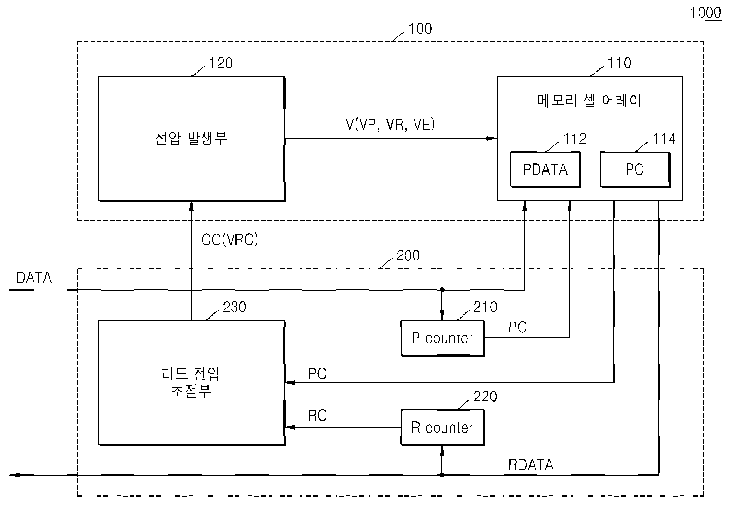
도 1를 참조하면, 본 발명에 따른 플래시 메모리 시스템(1000)은 플래시 메모리 장치(100) 및 메모리 컨트롤러(200)을 포함한다. 플래시 메모리 장치(100)는 메모리 셀 어레이(110) 및 전압 발생부(120)를 포함한다. Referring to FIG. 1, a
도 1은 플래시 메모리 시스템(1000)에 입출력되는 데이터의 흐름을 중심으로 도시된 것이다. 본 발명의 사상을 더욱 명확히 전달하기 위해, 플래시 메모리 시스템(1000) 내의 프로그램, 리드 및 소거를 위한 제어 신호들 또는 제어 명령들에 대해서는 구체적으로 설명하지 않는다. 그러나, 본 발명이 속하는 기술분야의 당업자들은 이러한 제어 신호들 또는 제어 명령들이 도시되지 않더라도 본 발명을 잘 이해할 수 있을 것이다.1 is a diagram illustrating a flow of data input and output to and from a
플래시 메모리 장치(100)의 메모리 셀 어레이(110)는 데이터가 저장되는 영역이다. 메모리 셀 어레이(110)는 워드라인과 비트라인에 연결된 복수의 메모리 셀들로 이루어진다. 하나의 메모리 셀은 한 비트 또는 하나 이상의 비트들을 저장할 수 있다. 하나의 메모리 셀이 하나의 비트를 저장하는 경우, 메모리 셀은 싱글 레벨 셀로 지칭될 수 있다. 하나의 메모리 셀이 복수의 비트를 저장하는 경우, 메모리 셀은 멀티 레벨 셀로 지칭될 수 있다. 하나의 멀티 레벨 셀이 M개의 비트들을 저장할 수 있는 경우, M비트 멀티 레벨 셀로 지칭될 수 있다. 여기서 M은 2이상의 정수일 수 있으며, 일반적으로, 2, 3 및 4 중 하나일 수 있다. The
메모리 셀 어레이(110)는 메인 영역(112) 및 스페어 영역(114)을 포함할 수 있다. 메인 영역(112)은 사용자가 액세스 가능한 사용자 데이터가 저장되는 영역이다. 스페어 영역(114)은 상기 사용자 데이터를 보조하기 위한, 예컨대, 오류 정정 정보와 같은 데이터, 또는 플래시 메모리 장치(100)의 관리에 필요한, 예컨대, 상태 정보나 불량 정보와 같은 데이터가 저장될 수 있다.The
도 1에 도시되지는 않았지만, 메모리 셀 어레이(110)는 메모리 셀들에 연결된 워드라인들과 비트라인들을 포함하며, 상기 워드라인들에 연결된 워드라인 디코더/드라이버(미 도시) 및 상기 비트라인들에 연결된 비트라인 디코더/드라이버(미 도시)를 주변 회로로서 포함할 수 있다. 상기 워드라인 디코더/드라이버는 메모리 셀 어레이(110)의 워드라인들 중에서, 액세스하고자 하는 어드레스에 대응되는 워드라인을 활성화할 수 있으며, 상기 비트라인 디코더/드라이버는 메모리 셀 어레이(110)의 비트라인들 중에서 액세스하고자 하는 어드레스에 대응되는 비트라인을 활성화할 수 있다. Although not shown in FIG. 1, the
메모리 컨트롤러(200)는 반도체 메모리 장치(100)의 메모리 셀 어레이(110)에 데이터가 프로그램되고 메모리 셀 어레이(110)로부터 데이터가 리드되는 것을 제어할 수 있다. 메모리 컨트롤러(200)는 메모리 셀 어레이(110)의 메인 영역(112)에 프로그램할 데이터(DATA)를 외부로부터 수신할 수 있으며, 메모리 셀 어레이(110)의 메인 영역(112)으로부터 리드된 데이터(RDATA)를 외부로 송신할 수 있다. 도 1에서 메모리 컨트롤러(200)는 플래시 메모리 장치(100)의 외부에 위치하는 메모리 컨트롤러 칩으로 구현되는 것으로 도시되어 있지만, 메모리 컨트롤러(200)는 플래시 메모리 장치(100) 내의 주변회로(Peripheral Circuit)로 구현될 수도 있다.The
도 1에 도시되지는 않았지만, 메모리 컨트롤러(200)는 외부로부터 예컨대, 프로그램 명령, 리드 명령, 및 소거 명령과 같은 제어 명령을 수신할 수 있다. 이러한 제어 명령에는 상기 제어 명령이 수행될 어드레스가 포함될 수 있다. 이러한 어드레스는 데이터(DATA)를 프로그램하거나, 리드하거나, 소거할 메모리 셀 어레이(110)의 논리적 또는 물리적 위치를 나타낼 수 있다. 메모리 컨트롤러(200)는 상기 어드레스를 상기 워드라인 디코더/드라이버 및 상기 비트라인 디코더/드라이버로 전달할 수 있으며, 이에 대응하여 상기 워드라인 디코더/드라이버 및 상기 비트라인 디코더/드라이버는 각각 대응하는 워드라인 및 비트라인을 활성화시킬 수 있다.Although not shown in FIG. 1, the
또한, 메모리 컨트롤러(200)는 제어 명령 및 데이터(DATA)에 대응되는 제어 신호(CC)를 플래시 메모리 장치(100)로 전송할 수 있다. 플래시 메모리 장치(100)의 전압 발생부(120)는 이러한 제어 신호(CC)에 응답하여, 메모리 셀 어레이(110)에 구동 전압(V)을 제공할 수 있다. 구동 전압(V)은 프로그램 전압(VP), 리드 전압(VR) 및 소거 전압(VE) 등을 포함할 수 있다.In addition, the
메모리 컨트롤러(200)는 데이터(DATA)를 수신할 수 있으며, 데이터(DATA)가 플래시 메모리 장치(100)의 메모리 셀 어레이(110)에 저장되도록 제어할 수 있다. 데이터(DATA)는 메모리 셀 어레이(110)의 메인 영역(112)에 저장될 수 있으며, 메모리 셀 어레이(110)에 프로그램되어 있는 데이터는 프로그램 데이터(PDATA)로 지칭될 수 있다. 또한, 메모리 컨트롤러(200)는 플래시 메모리 장치(100)의 메모리 셀 어레이(110)로부터 프로그램 데이터(PDATA)가 리드되도록 제어할 수 있으며, 메모리 셀 어레이(110)로부터 리드된 데이터를 리드 데이터(RDATA)로서 외부로 제공할 수 있다.The
그러나, 메모리 셀 어레이(110)에 저장되어 있는 정보는 시간이 많이 흐르거나 플래시 메모리 시스템(1000)의 내구연한에 도달함에 따라 초기에 저장된 셀 산포들에서 달라질 수 있다. 또한, 주변 메모리 셀들에 대한 액세스로 인하여 셀 산포가 달라질 수도 있다. 그 결과, 메모리 셀 어레이(110)에 프로그램된 프로그램 데이터(PDATA)와 메모리 셀 어레이(110)로부터 리드된 리드 데이터(RDATA)가 서로 일치하지 않을 수 있다. 이러한 불일치를 제거하기 위한 한 방법으로서, 메모리 셀 어레이(110)의 스페어 영역(114)에는 오류 정정 정보가 저장될 수 있다. 그러나 오류 정정 정보에 의해서도 정정될 수 없는 경우가 있다. 그러나, 본 발명에 따르면 프로그램 카운트 정보(PC)를 이용하여 오류 정정의 가능성을 더욱 높일 수 있다. 이러한 프로그램 카운트 정보(PC)는 스페어 영역(114)에 저장될 수 있다.However, the information stored in the
또한, 메모리 컨트롤러(200)는 프로그램 카운트 정보(PC)를 이용하여 전압 발생부(120)가 제공하는 리드 전압의 전압 레벨을 보상하기 위한 전압 레벨 보상 신호(VRC)를 생성할 수 있다. 전압 레벨 보상 신호(VRC)는 제어 명령의 형태로 플래시 메모리 장치(100)의 전압 발생부(120)로 전송될 수 있다.In addition, the
프로그램 전압(VP)은 메모리 셀들이 도 2에 도시되는 바와 같이, 비트 값에 대응하는 문턱 전압의 산포를 갖도록 설정될 수 있다.The program voltage VP may be set such that the memory cells have a distribution of threshold voltages corresponding to bit values, as shown in FIG. 2.
도 2의 (a)는 싱글 레벨 셀(이하 'SLC'로 지칭) 플래시 메모리 장치에서의 셀 산포를 나타내고, 도 2의 (b) 및 (c)는 멀티 레벨 셀(이하 'MLC'로 지칭) 플래시 메모리 장치에서의 셀 산포를 나타낸다. MLC 플래시 메모리 장치는 하나의 메모리 셀에 2개 이상의 비트들이 프로그램 된다. 도 2의 (b)는 2-비트 MLC 플래시 메모리 장치에서의 셀 산포를 나타내고, 도 2의 (c)는 3-비트 MLC 플래시 메모리 장치에서의 셀 산포를 나타낸다.FIG. 2A illustrates a cell distribution in a single level cell (hereinafter referred to as 'SLC') flash memory device, and FIGS. 2B and 2C illustrate a multilevel cell (hereinafter referred to as 'MLC'). Represents a cell spread in a flash memory device. In an MLC flash memory device, two or more bits are programmed in one memory cell. FIG. 2B shows a cell spread in a 2-bit MLC flash memory device, and FIG. 2C shows a cell spread in a 3-bit MLC flash memory device.
도 2의 (a)의 경우, SLC 메모리 셀들은 2개의 상태("E(Erase)" 및 "P(Program)") 중 하나의 상태를 가질 수 있다. 반면, 도 2의 (b)의 경우, 2비트 MLC 메모리 셀들은 4개의 상태들("E","P1", "P2" 및 "P3") 중 하나의 상태를 가질 수 있다. 또한, 도 2의 (c)의 경우, 3비트 메모리 셀들은 여덟 개의 상태들("E","P1"~"P7") 중 하나의 상태를 가질 수 있다.In the case of FIG. 2A, the SLC memory cells may have one of two states (“E (Erase)” and “P (Program)”). In contrast, in FIG. 2B, 2-bit MLC memory cells may have one of four states “E”, “P1”, “P2”, and “P3”. In addition, in FIG. 2C, the 3 bit memory cells may have one of eight states “E”, “P1” to “P7”.
아래에서 별도의 언급이 없으면, MLC 플래시 메모리 장치의 일반적인 동작을 설명함에 있어, 2-비트 MLC 플래시 메모리 장치를 중심으로 설명한다. Unless otherwise mentioned below, the general operation of the MLC flash memory device will be described with reference to a 2-bit MLC flash memory device.
하나의 메모리 셀에 프로그램되는 2개의 비트들은 상위 비트(upper bit)와 하위 비트(lower bit)를 포함할 수 있다. 상위 비트에 대한 페이지와 하위 비트에 대한 페이지는 메모리 셀 어레이(110)에서 동일한 워드 라인에 연결되는 메모리 셀들에 프로그램된다. 다만, 일반적으로 상위 비트와 하위 비트는 서로 다른 2개의 다른 페이지에 포함되므로, 하나의 메모리 셀에 프로그램되는 상위 비트와 하위 비트는 논리적으로 서로 다른 페이지 어드레스에 의하여 프로그램된다. Two bits programmed in one memory cell may include an upper bit and a lower bit. The page for the upper bit and the page for the lower bit are programmed in memory cells connected to the same word line in the
2-비트 MLC 플래시 메모리 장치에서의 프로그램 동작을 설명하기 위한 도 3에 도시되는 바와 같이, 복수의 메모리 셀들에 대한 제1 페이지의 프로그램이 수행된 후에, 제1 페이지의 셀 산포로부터 제2 페이지에 대한 프로그램이 수행될 수 있다. 도 3에서 상위 비트에 대한 페이지를 제1 페이지로 예시하였고, 하위 비트에 대한 페이지를 제2 페이지로 예시하였다. 그러나, 프로그램되는 페이지의 순서는 플래시 메모리 장치(100)의 설계에 따라 달라질 수 있다.As shown in FIG. 3 for explaining the program operation in the 2-bit MLC flash memory device, after the program of the first page for the plurality of memory cells is performed, Program can be performed. In FIG. 3, a page for upper bits is illustrated as a first page, and a page for lower bits is illustrated as a second page. However, the order of pages to be programmed may vary depending on the design of the
본 명세서에서 제1 페이지는 메모리 셀들에 처음으로 프로그램되는 페이지를 의미하고, 제2 페이지는 제1 페이지가 아닌 다른 페이지를 의미한다. 2-비트 MLC 플래시 메모리 장치의 경우, 제2 페이지는 메모리 셀들에 두 번째로 프로그램되는 페이지를 의미한다. 그러나, 3비트 이상의 MLC 플래시 메모리 장치의 경우, 제2 페이지는 메모리 셀들에 두 번째로 프로그램되는 페이지를 의미할 수도 있고, 메모리 셀들에 마지막으로 프로그램되는 페이지일 수도 있다.In the present specification, the first page refers to a page programmed into memory cells for the first time, and the second page refers to a page other than the first page. In the case of a 2-bit MLC flash memory device, a second page means a page programmed second in memory cells. However, in the case of an MLC flash memory device having 3 bits or more, the second page may mean a page programmed second in the memory cells, or may be a page last programmed in the memory cells.
프로그램이 수행되기 전에 모든 메모리 셀들은 "E" 상태를 갖는다. 복수의 메모리 셀들에 대한 제1 페이지의 프로그램이 수행되면, 해당하는 비트의 논리 값이 0인 메모리 셀들은 "P" 상태를 갖도록 프로그램되고, 해당하는 비트의 논리 값이 1인 메모리 셀들은 "E" 상태를 유지한다.All memory cells have an "E" state before the program is performed. When a program of a first page for a plurality of memory cells is executed, memory cells having a logic value of a corresponding bit of 0 are programmed to have a "P" state, and memory cells having a logic value of a corresponding bit of "E" are referred to as "E". "Maintain state.
그 후, 제2 페이지의 프로그램이 수행되면, 메모리 셀들은 "E" 상태, "P1" 상태, "P2" 상태 및 "P3" 상태 중 하나를 갖게 된다. 이 때, 제1 페이지에서 비트의 논리 값이 1이고 제2 페이지에서 비트의 논리 값이 1인 메모리 셀들은 "E" 상태를 유지하고, 제1 페이지에서 비트의 논리 값이 1이고 제2 페이지에서 비트의 논리 값이 0인 메모리 셀들은 "P1" 상태를 갖도록 프로그램된다. 또한, 제1 페이지에서 비트의 논리 값이 0이고 제2 페이지에서 비트의 논리 값이 0인 메모리 셀들은 "P"상태에서 "P2" 상태로 프로그램되고, 제1 페이지에서 비트의 논리 값이 0이고 제2 페이지에서 비트의 논리 값이 1인 메모리 셀들은 "P"상태에서 "P3" 상태로 프로그램된다.Thereafter, when the program of the second page is performed, the memory cells have one of the "E" state, the "P1" state, the "P2" state, and the "P3" state. At this time, memory cells having a logic value of 1 in the first page and a logic value of 1 in the second page remain in the "E" state, and the logic value of the bit in the first page is 1 and the second page. Are programmed to have a " P1 " state. In addition, memory cells having a logic value of 0 on the first page and a logic value of 0 on the second page are programmed from the "P" state to the "P2" state, and the logic value of the bit on the first page is 0. Memory cells with a logic value of 1 in the second page are programmed from the "P" state to the "P3" state.
이와 같이 제1 페이지의 프로그램과 제2 페이지의 프로그램이 끝난 메모리 셀들은 도 2의 (b)와 같은 셀 산포를 갖게 된다. 이들의 논리 값을 리딩하기 위해, 리드 전압들(VR1, VR21, VR22)이 이용될 수 있다. 리드 전압(VR1)을 인가하면, "E" 상태와 "P1" 상태를 갖는 메모리 셀들은 턴 온되고, "P2" 상태와 "P3" 상태를 갖는 메모리 셀들은 턴 오프된다. 이를 감지함으로써, 해당 메모리 셀의 제1 페이지의 비트 값이 0인지 1인지를 파악할 수 있다. 즉, 리드 전압(VR1)을 인가할 때, 메모리 셀이 턴 온된다면, 상기 메모리 셀에 저장된 데이터의 상위 비트는 1이고, 메모리 셀이 턴 오프된다면, 상기 메모리 셀에 저장된 데이터의 상위 비트는 0이다.As such, the memory cells that have completed the program of the first page and the program of the second page have cell dispersions as shown in FIG. To read their logic values, read voltages VR1, VR21, VR22 can be used. When the read voltage VR1 is applied, memory cells having an "E" state and a "P1" state are turned on, and memory cells having a "P2" state and a "P3" state are turned off. By detecting this, it is possible to determine whether the bit value of the first page of the corresponding memory cell is 0 or 1. FIG. That is, when the memory cell is turned on when the read voltage VR1 is applied, the upper bit of the data stored in the memory cell is 1, and when the memory cell is turned off, the upper bit of the data stored in the memory cell is 0. to be.
제2 페이지의 논리 값들을 알기 위해서 리드 전압들(VR21, VR22)이 이용될 수 있다. 리드 전압(VR21)을 인가할 때의 메모리 셀의 온/오프 상태와 리드 전압(VR22)을 인가할 때의 메모리 셀의 온/오프 상태가 동일하면, 상기 메모리 셀에 저장된 데이터의 하위 비트는 1이고, 온/오프 상태들이 서로 다르면 상기 메모리 셀에 저장된 데이터의 하위 비트는 0이다.The read voltages VR21 and VR22 may be used to know the logic values of the second page. If the on / off state of the memory cell when applying the read voltage VR21 and the on / off state of the memory cell when applying the read voltage VR22 are the same, the lower bit of the data stored in the memory cell is 1; When the on / off states are different from each other, the lower bit of the data stored in the memory cell is zero.
마찬가지로, 3-비트 MLC 플래시 메모리 장치는 도 4에 도시되는 바와 같이, 제1 페이지 및 제2 페이지에 대한 프로그램을 수행한 후, 제3 페이지에 대한 프로그램을 수행할 수 있다. 4-비트 MLC 플래시 메모리 장치도, 같은 방식으로 복수개의 비트들에 대하여 프로그램을 수행할 수 있다.Similarly, as illustrated in FIG. 4, the 3-bit MLC flash memory device may perform a program for a first page and a second page, and then execute a program for a third page. A 4-bit MLC flash memory device can also program on a plurality of bits in the same manner.
리드의 경우에도, 2-비트 MLC 플래시 메모리 장치와 유사하게, 리드 전압(VR1)을 이용하여 메모리 셀에 저장된 제1 비트의 논리 값을 파악할 수 있다. 또한, 리드 전압들(VR21, VR22)을 이용하여 메모리 셀에 저장된 제2 비트의 논리 값을 파악할 수 있다. 또한, 메모리 셀에 저장된 제3 비트의 논리 값을 파악하기 위해, 리드 전압들(VR31, VR32, VR33)이 이용될 수 있다. 여기서, 제1 비트는 제1 페이지 프로그램에 의해 저장되는 비트이고, 제2 비트는 제2 페이지 프로그램에 의해 저장되는 비트이고, 제3 비트는 제3 페이지 프로그램에 의해 저장되는 비트이다.In the case of a read, similar to the 2-bit MLC flash memory device, the read voltage VR1 may be used to determine a logic value of the first bit stored in the memory cell. In addition, the logic values of the second bits stored in the memory cell may be determined using the read voltages VR21 and VR22. In addition, read voltages VR31, VR32, and VR33 may be used to determine the logic value of the third bit stored in the memory cell. Here, the first bit is a bit stored by the first page program, the second bit is a bit stored by the second page program, and the third bit is a bit stored by the third page program.
도 3과 도 4에 도시되는 프로그램 방법은 예시적인 것으로 본 발명을 한정하지 않는다. 다만, 아래의 설명에서, 본 발명을 쉽게 이해시키기 위해 도 3과 도 4에 예시적으로 도시된 방법에 의하여 플래시 메모리 셀들이 프로그램되는 것으로 가정하여 설명한다.The program methods shown in Figs. 3 and 4 are exemplary and do not limit the present invention. However, in the following description, it is assumed that the flash memory cells are programmed by the method illustrated in FIGS. 3 and 4 to easily understand the present invention.
다시 도 1을 참조하면, 메모리 컨트롤러(200)는 프로그램 카운터(210), 리드 카운터(220) 및 리드 전압 조절부(230)를 포함할 수 있다. Referring back to FIG. 1, the
프로그램 카운터(210)는 메모리 컨트롤러(200)에 수신된 데이터(DATA)의 비트들 중에서 제1 논리 값을 갖는 비트들의 개수를 계수할 수 있다. 구체적으로, 프로그램 카운터(210)는 데이터(DATA)를 오류 정정 단위로 제1 논리 값을 갖는 비트들의 개수를 계수할 수 있다. The
여기서, 오류 정정 단위는 메모리 컨트롤러(200)에 의해 데이터의 오류를 정정하는 단위이다. 예컨대, 메모리 컨트롤러(200)는 하나의 페이지 단위로 데이터의 오류를 정정할 수 있다. 또한, 복수의 페이지 단위로도 오류가 정정될 수 있으며, 블록 단위로도 오류가 정정될 수 있다. 또한, 하나의 페이지에 둘 이상의 섹터가 포함된 경우에는 섹터 단위로 오류를 정정할 수도 있다. 아래에서는 한 페이지 단위로 데이터의 오류가 정정되는 것으로 가정하여 설명한다. 그러나, 본 발명에서는 반드시 페이지 단위로 오류가 정정되어야 한다거나, 프로그램 카운터(210)가 페이지 단위의 데이터에서 제1 논리 값을 갖는 비트들의 개수를 계수하여야만 하는 것은 아니다. 즉, 섹터 단위로 섹터에 포함된 제1 논리 값ㅇ르 갖는 비트들의 개수를 계수할 수도 있다.Here, the error correction unit is a unit for correcting an error of data by the
제1 논리 값은 논리 하이 또는 논리 로우일 수 있다. 즉, 제1 논리 값은 "1"일 수도 있고, "0"일 수도 있다. 다만, 제1 논리 값을 편의상 소거 상태에 대응하는 논리 값으로 가정한다. 즉, 도 3 및 도 4에 도시된 예에 따라, 제1 논리 값은 "1"인 것으로 가정한다.The first logical value may be logic high or logic low. That is, the first logical value may be "1" or "0". However, it is assumed that the first logic value is a logic value corresponding to the erase state for convenience. That is, according to the examples shown in FIGS. 3 and 4, it is assumed that the first logical value is "1".
프로그램 카운터(210)는 수신된 데이터(DATA)를 페이지 단위로 논리 값이 "1"인 비트들의 개수를 계수할 수 있다. 이러한 계수 정보는 프로그램 카운트 정보(PC)로 명명될 수 있으며, 도 1에 도시된 바와 같이, 프로그램 카운트 정보(PC)는 메모리 셀 어레이(110)의 스페어 영역(114)에 저장될 수 있다. 그러나 프로그램 카운트 정보(PC)가 반드시 스페어 영역(114)에 저장되어야 하는 것은 아니며, 메인 영역(112)에 프로그램 데이터(PDATA)와 함께 저장될 수도 있다.The
또한, 프로그램 데이터(PDATA)는 프로그램 카운트 정보(PC)가 산출된 데이터를 지칭할 수 있다. 프로그램 데이터(PDATA)는 페이지 단위의 데이터일 수 있다. 이 경우, 프로그램 데이터(PDATA)와 프로그램 카운트 정보(PC)는 동일한 워드라인에 연결된 메모리 셀들에 저장될 수 있다. 또한, 프로그램 데이터(PDATA)가 메모리 셀들의 임의의 워드라인에 연결된 메모리 셀들의 제1 페이지에 프로그램된다면, 프로그램 카운트 정보(PC)도 역시 동일한 워드라인에 연결된 메모리 셀들의 동일한 페이지, 즉, 상기 메모리 셀들의 제1 페이지에 저장될 수 있다.In addition, the program data PDATA may refer to data from which program count information PC is calculated. The program data PDATA may be data in a page unit. In this case, the program data PDATA and the program count information PC may be stored in memory cells connected to the same word line. Further, if program data PDATA is programmed in a first page of memory cells connected to any word line of memory cells, then program count information PC is also the same page of memory cells connected to the same word line, i.e., the memory. May be stored in a first page of cells.
메모리 컨트롤러(200)는 메모리 셀 어레이(110)에 저장된 프로그램 데이터(PDATA)를 리드할 수 있다. 이 때, 메모리 컨트롤러(200)는 프로그램 데이터(PDATA)에 대응하는 프로그램 카운트 정보(PC)도 함께 리드할 수 있다. 메모리 컨트롤러(200)에 의해 리드된 데이터는 리드 데이터(RDATA)로 지칭될 수 있다. 상술한 바와 같이, 메모리 셀들의 산포 변화로 인하여, 프로그램 데이터(PDATA)와 리드 데이터(RDATA)는 서로 상이할 수 있다.The
리드 카운터(220)는 리드 데이터(RDATA)의 비트들 중에서 제1 논리 값을 갖는 비트들의 개수를 계수할 수 있다. 이 계수 값은 리드 카운트 정보(RC)로 지칭될 수 있으며, 프로그램 카운트 정보(PC)와 함께 리드 전압 조절부(230)로 제공될 수 있다.The
리드 전압 조절부(230)는 리드 카운트 정보(RC)와 프로그램 카운트 정보(PC)를 비교하여, 이들의 차이를 산출하고, 산출된 차이 값을 기초로 리드 전압의 전압 레벨을 조절하기 위한 전압 레벨 보상 신호(VRC)를 생성할 수 있다. 전압 레벨 보상 신호(VRC)는 플래시 메모리 장치(100)의 전압 발생부(120)로 제공되며, 전압 발생부(120)는 전압 레벨 보상 신호 (VRC)에 응답하여, 메모리 셀 어레이(110)로부터 프로그램 데이터(PDATA)를 리드하기 위한 리드 전압(VR)을 조절할 수 있다.
The read
도 5는 본 발명의 다른 실시예에 따른 플래시 메모리 시스템을 간략히 보여주는 블록도이다.5 is a block diagram schematically illustrating a flash memory system according to another exemplary embodiment of the present invention.
도 5를 참조하면, 플래시 메모리 시스템(1000a)는 플래시 메모리 장치(100) 및 메모리 컨트롤러(200a)를 포함한다. 플래시 메모리 장치(100)는 메모리 셀 어레이(110) 및 전압 발생부(120)를 포함한다. 도 5에 도시된 플래시 메모리 시스템(1000a)는 도 1에 도시된 플래시 메모리 시스템(1000)와 실질적으로 유사하며, 차이가 나는 부분을 중심으로 설명하며, 반복되는 부분에 대한 설명은 도 1에 대한 설명으로 갈음한다.Referring to FIG. 5, the
메모리 컨트롤러(200a)는 프로그램 카운터(210), 리드 카운터(220) 및 리드 전압 조절부(230)를 포함한다. 또한, 메모리 컨트롤러(200a)는 제1 랜덤화부(240) 및 제2 랜덤화부(250), 및 이들에 상응하는 제1 디랜덤화부(260) 및 제2 디랜덤화부(270)를 더 포함할 수 있다.The
메모리 컨트롤러(200a)는 데이터(DATA)를 수신할 수 있다. 제1 랜덤화부(240)는 수신된 데이터(DATA)를 랜덤화하여 랜덤 데이터(DATA_R)를 생성한다. 랜덤 데이터(DATA_R)는 메모리 셀 어레이(110)의 메인 영역(112)에 프로그램될 수 있다. 메인 영역(120)에 프로그램된 랜덤 데이터(DATA_R)는 랜덤 프로그램 데이터(PDATA_R)로 지칭될 수 있다. 제1 랜덤화부(240)는 수신된 데이터(DATA)의 비트 값들을 랜덤하게 재설정하는 랜덤화 동작을 수행한다. 그에 따라 랜덤 데이터(DATA_R)의 비트 값들은 확률적으로 동일한 분포를 갖는다. 즉, 랜덤 데이터(DATA_R)의 비트들은 약 50%가 "0"의 논리 값을 갖고 나머지 약 50%가 "1"의 논리 값을 갖는다.The
프로그램 카운터(210)는 랜덤 데이터(DATA_R)를 수신하여, 랜덤 데이터(DATA_R)의 비트들 중에서 제1 논리 값을 갖는 비트들의 개수를 계수할 수 있다. 제1 논리 값을 갖는 비트들의 개수는 프로그램 카운트 정보(PC)로 지칭될 수 있다. 그러나, 랜덤 데이터(DATA_R)의 길이는 페이지의 길이와 동일할 수 있으며, 이 경우, 랜덤 데이터(DATA_R)의 총 비트 수는 이미 결정되어 있다. 즉, 랜덤 데이터(DATA_R)의 총 비트 수는 페이지의 크기와 하나의 메모리 셀에 저장되는 비트의 개수의 곱과 동일할 수 있다. 따라서, 프로그램 카운트 정보(PC)는 대략 1/2이라고 가정할 수 있다. 이 경우, 프로그램 카운터(210)는 생략될 수 있고, 프로그램 카운트 정보(PC)는 한 페이지의 비트들의 개수의 1/2로 가정될 수 있다.The
프로그램 카운트 정보(PC)는 제2 랜덤화부(250)에 의해 랜덤화되어 랜덤 프로그램 카운트 정보(PC_R)로 변형될 수 있으며, 랜덤 프로그램 카운트 정보(PC_R)는 메모리 셀 어레이(110)의 스페어 영역(114)에 프로그램될 수 있다.The program count information PC may be randomized by the
제2 디랜덤화부(270)는 스페어 영역(114)에 프로그램된 랜덤 프로그램 카운트 정보(PC_R)를 리드하여 이를 프로그램 카운트 정보(PC)로 복원할 수 있다. 프로그램 카운트 정보(PC)는 리드 전압 조절부(230)에 제공될 수 있다. 상술한 바와 같이, 제1 랜덤화부(240)에 의하여 랜덤 데이터(DATA_R)의 제1 논리 값을 갖는 비트들의 개수가 전체 비트들의 개수의 1/2에 근접할 것이다. 따라서, 프로그램 카운트 정보(PC)는 전체 비트들의 개수의 1/2로 가정할 수 있으며, 그 경우, 프로그램 카운터(210), 제2 랜덤화부(250) 및 제2 디랜덤화부(270)는 생략될 수 있으며, 프로그램 카운트 정보(PC)가 메모리 셀 어레이(110)에 저장될 필요도 없다.The
메인 영역(112)에 저장된 랜덤 프로그램 데이터(PDATA_R)가 리드되면서, 랜덤 프로그램 데이터(PDATA_R)는 랜덤 리드 데이터(RDATA_R)로 리드될 수 있다. 상술한 바와 같이, 랜덤 프로그램 데이터(PDATA_R)와 랜덤 리드 데이터(RDATA_R)는 서로 상이할 수 있다. 리드 카운터(220)는 랜덤 리드 데이터(RDATA_R)의 비트들 중에서 제1 논리 값을 갖는 비트들의 개수를 계수하여, 리드 카운트 정보(RC)를 생성할 수 있다. 리드 카운트 정보(RC)는 리드 전압 조절부(230)에 제공될 수 있다.As the random program data PDATA_R stored in the
또한, 랜덤 리드 데이터(RDATA_R)는 제1 디랜덤화부(260)에 의하여 리드 데이터(RDATA)로 복원될 수 있으며, 리드 데이터(RDATA)는 메모리 컨트롤러(200a)에 의해 외부로 송신될 수 있다.In addition, the random read data RDATA_R may be restored to the read data RDATA by the
리드 전압 조절부(230)는 메모리 셀 어레이(110)에 저장된 랜덤 프로그램 데이터(PDATA_R)에 대한 프로그램 카운트 정보(PC)와 메모리 셀 어레이(110)로부터 리드된 랜덤 리드 데이터(RDATA_R)에 대한 리드 카운트 정보(RC)를 이용하여 리드 전압(VR)을 조절할 수 있다.
The read
도 6a 내지 6f는 본 발명의 실시예들을 설명하기 위해 메모리 셀들의 산포들을 예시적으로 도시한다.6A-6F illustrate distributions of memory cells to illustrate embodiments of the present invention.
도 6a 내지 도 6e는 2비트 MLC 방식의 메모리 셀들에 프로그램이 끝난 단계의 셀 산포들을 도시하며, 도 6f는 3비트 MLC 방식의 메모리 셀들에 프로그램이 끝난 단계의 셀 산포들을 도시한다.6A through 6E illustrate cell distributions of a programmed step in memory cells of 2 bit MLC method, and FIG. 6F illustrates cell distributions of a programmed step in memory cells of 3 bit MLC method.
도 6a를 참조하면, 도 2의 (b)에 도시된 산포들과 비교할 때, "E" 상태, "P1" 상태, "P2" 상태 및 "P3" 상태의 산포들이 리드 전압들(VR21, VR1, VR22)을 넘어 옆으로 퍼져있다. 이는 전자를 플로팅 게이트와 같은 전하 저장층에 저장하는 플래시 메모리 장치의 특성상 전자들이 전하 저장층에서 누설되거나 과잉 공급됨에 따라 생기는 현상이다. 이 경우, 리드 전압(R21)을 초과하는 "E" 상태의 산포 부분과 리드 전압(R21) 이하로 내려온 "P1" 상태의 산포 부분은 리드 과정에서 오류를 일으킨다. 리드 전압(R1)과 리드 전압(R22)의 경우에도 마찬가지이다. 이러한 오류들은 오류 정정 정보에 의해 정정될 수 있다.Referring to FIG. 6A, the dispersions of the "E" state, the "P1" state, the "P2" state, and the "P3" state are compared with the dispersions shown in FIG. 2B, and the read voltages VR21 and VR1. , VR22 is spread sideways beyond. This is a phenomenon that occurs due to leakage or oversupply of electrons in the charge storage layer due to the characteristics of the flash memory device which stores the electrons in the charge storage layer such as the floating gate. In this case, the spread portion in the "E" state exceeding the read voltage R21 and the spread portion in the "P1" state below the read voltage R21 cause an error in the read process. The same applies to the read voltage R1 and the read voltage R22. These errors can be corrected by the error correction information.
도 6b를 참조하면, 도 6b에 도시된 각 산포들은 도 6a에 도시된 산포들에 비하여 좌측으로 치우쳐있다. 리드 전압(VR1)으로 메모리 셀의 제1 페이지에 저장된 데이터의 비트들의 값을 검출하면, 초기보다 "1"의 논리 값을 갖는 비트들이 많아진다. 즉, "1"의 논리 값을 갖는 비트들의 개수를 계수할 경우, 제1 페이지에 대한 리드 카운트 정보(RC)는 제1 페이지에 대한 프로그램 카운트 정보(PC)보다 많다.Referring to FIG. 6B, each of the dispersions shown in FIG. 6B is biased to the left as compared to the dispersions shown in FIG. 6A. When the value of the bits of the data stored in the first page of the memory cell is detected by the read voltage VR1, more bits having a logic value of "1" than the initial stage become larger. That is, when counting the number of bits having a logical value of "1", the read count information RC for the first page is larger than the program count information PC for the first page.
이러한 현상은 메모리 셀에 저장된 전하들이 시간이 흐름에 따라 누설되면서 일어날 수 있다. 이러한 현상은 어느 한 산포에서 나타나는 것이 아니라 모든 산포에서 걸쳐 나타날 수 있다. 따라서, 리드 전압들(VR21, VR1, VR22)을 새로운 리드 전압들(nVR21, nVR1, nVR22)로 수정하는 것이 필요하며, 이를 위해, 전압 레벨 보상 값들(-ΔVR21, -ΔVR1, -ΔVR22)이 적용될 수 있다. This can happen as the charges stored in the memory cell leak over time. This phenomenon does not occur at any one spread, but can occur at all spreads. Therefore, it is necessary to modify the read voltages VR21, VR1, VR22 to new read voltages nVR21, nVR1, nVR22, and for this, voltage level compensation values (-ΔVR21, -ΔVR1, -ΔVR22) are applied. Can be.
도 6b의 그래프로부터 알 수 있겠지만, 전압 레벨 보상 값들(-ΔVR21, -ΔVR1, -ΔVR22)은 리드 카운트 정보(RC)와 프로그램 카운트 정보(PC)의 차이에 비례할 수 있다. 또한, 전압 레벨 보상 값들(-ΔVR21, -ΔVR1, -ΔVR22)은 리드 카운트 정보(RC)와 프로그램 카운트 정보(PC)의 차이에 따라 미리 정의된 리드 리트라이 테이블(Read Retry Table)을 이용하여 결정될 수 있다. 이러한 리드 리트라이 테이블은 도 8을 참조로 설명된다.As can be seen from the graph of FIG. 6B, the voltage level compensation values -ΔVR21, -ΔVR1, and -ΔVR22 may be proportional to the difference between the read count information RC and the program count information PC. In addition, the voltage level compensation values (-ΔVR21, -ΔVR1, -ΔVR22) may be determined using a read retry table defined in advance according to the difference between the read count information RC and the program count information PC. Can be. This read retry table is described with reference to FIG. 8.
도 6c를 참조하면, 도 6c에 도시된 각 산포들은 도 6a에 도시된 산포들에 비하여 우측으로 치우쳐있다. 리드 전압(VR1)으로 메모리 셀의 제1 페이지에 저장된 데이터의 비트들의 값을 검출하면, 초기보다 "1"의 논리 값을 갖는 비트들이 적어진다. 즉, "1"의 논리 값을 갖는 비트들의 개수를 계수할 경우, 제1 페이지에 대한 리드 카운트 정보(RC)는 제1 페이지에 대한 프로그램 카운트 정보(PC)보다 적다.Referring to FIG. 6C, each of the dispersions shown in FIG. 6C is biased to the right as compared to the dispersions shown in FIG. 6A. When the value of the bits of data stored in the first page of the memory cell is detected by the read voltage VR1, the bits having a logic value of "1" are fewer than the initial one. That is, when counting the number of bits having a logic value of "1", the read count information RC for the first page is less than the program count information PC for the first page.
이러한 현상은 메모리 셀에 대한 프로그램/소거 동작을 반복함에 따라 게이트 절연층이 취약해지면서 일어날 수 있다. 이러한 현상은 어느 한 산포에서 나타나는 것이 아니라 모든 산포에서 걸쳐 나타날 수 있다. 따라서, 리드 전압들(VR21, VR1, VR22)을 새로운 리드 전압들(nVR21, nVR1, nVR22)로 수정하는 것이 필요하며, 이를 위해, 전압 레벨 보상 값들(+ΔVR21, +ΔVR1, +ΔVR22)이 적용될 수 있다. This may occur as the gate insulating layer becomes vulnerable as the program / erase operations for the memory cells are repeated. This phenomenon does not occur at any one spread, but can occur at all spreads. Therefore, it is necessary to modify the read voltages VR21, VR1, VR22 to new read voltages nVR21, nVR1, nVR22, and for this, voltage level compensation values + ΔVR21, + ΔVR1, + ΔVR22 are applied. Can be.
도 6c의 그래프로부터 알 수 있겠지만, 전압 레벨 보상 값들(+ΔVR21, +ΔVR1, +ΔVR22)은 리드 카운트 정보(RC)와 프로그램 카운트 정보(PC)의 차이에 비례할 수 있다. 또한, 전압 레벨 보상 값들(+ΔVR21, +ΔVR1, +ΔVR22)은 리드 카운트 정보(RC)와 프로그램 카운트 정보(PC)의 차이에 따라 미리 정의된 리드 리트라이 테이블(Read Retry Table)을 이용하여 결정될 수 있다.As can be seen from the graph of FIG. 6C, the voltage level compensation values + ΔVR21, + ΔVR1, and + ΔVR22 may be proportional to the difference between the read count information RC and the program count information PC. In addition, the voltage level compensation values + ΔVR21, + ΔVR1, and + ΔVR22 may be determined using a read retry table defined in advance according to the difference between the read count information RC and the program count information PC. Can be.
도 6d를 참조하면, 도 6d에 도시된 "E" 상태의 산포는 도 6a에 도시된 "E" 상태의 산포에 비하여 우측으로 치우쳐있다. 리드 전압(VR1)으로 메모리 셀의 제1 페이지에 저장된 데이터의 비트들의 값을 검출하면, 프로그램 시와 비교할 때 "1"의 논리 값을 갖는 비트들의 수는 거의 동일하다. 즉, "1"의 논리 값을 갖는 비트들의 개수를 계수할 경우, 제1 페이지에 대한 리드 카운트 정보(RC)는 제1 페이지에 대한 프로그램 카운트 정보(PC)와 거의 비슷하다. 그러나, 리드 전압들(VR21, VR22)으로 메모리 셀의 제2 페이지에 저장된 데이터의 비트들의 값을 검출하면, 프로그램 시와 비교할 때 "1"의 논리 값을 갖는 비트들의 수는 적어진다. 즉, 제2 페이지에 대한 리드 카운트 정보(RC)는 제2 페이지에 대한 프로그램 카운트 정보(PC)보다 적다.Referring to FIG. 6D, the dispersion in the "E" state shown in FIG. 6D is biased to the right as compared to the dispersion in the "E" state shown in FIG. 6A. If the value of the bits of the data stored in the first page of the memory cell is detected with the read voltage VR1, the number of bits having a logic value of "1" is almost the same as compared with the programming time. That is, when counting the number of bits having a logical value of "1", the read count information RC for the first page is almost similar to the program count information PC for the first page. However, if the values of the bits of the data stored in the second page of the memory cell with the read voltages VR21 and VR22 are detected, the number of bits having a logic value of "1" becomes small when compared with the programming time. That is, the read count information RC for the second page is less than the program count information PC for the second page.
이러한 현상은 메모리 셀을 리드함에 따라 인접한 메모리 셀의 문턱 전압이 변하면서 일어날 수 있다. 특히, "E" 상태의 메모리 셀은 인접 메모리 셀에 가해지는 리드 전압의 영향으로 문턱 전압이 상승하게 된다. 이러한 현상은 리드 디스터번스(read disturbance)로 알려져 있다. 이러한 현상은 제1 페이지에 대한 프로그램 카운트 정보(PC)와 리드 카운트 정보(RC)의 차이는 미미하지만, 제2 페이지에 대한 프로그램 카운트 정보(PC)와 리드 카운트 정보(RC) 간에 차이가 생기는 것으로 감지할 수 있다. 따라서, 리드 전압(VR21)을 새로운 리드 전압(nVR21)로 수정하는 것이 필요하며, 이를 위해, 전압 레벨 보상 값(+ΔVR21)이 적용될 수 있다. This phenomenon may occur as the threshold voltages of adjacent memory cells change as the memory cells are read. In particular, the threshold voltage of the memory cell in the "E" state increases due to the read voltage applied to the adjacent memory cell. This phenomenon is known as read disturbance. This phenomenon is that the difference between the program count information PC and the read count information RC for the first page is small, but a difference occurs between the program count information PC and the read count information RC for the second page. It can be detected. Therefore, it is necessary to correct the read voltage VR21 to the new read voltage nVR21. For this purpose, a voltage level compensation value + ΔVR21 may be applied.
도 6d의 그래프로부터 알 수 있겠지만, 전압 레벨 보상 값(+ΔVR21)은 제2 페이지에 대한 리드 카운트 정보(RC)와 프로그램 카운트 정보(PC)의 차이에 비례할 수 있다. 또한, 전압 레벨 보상 값(+ΔVR21)은 제2 페이지에 대한 리드 카운트 정보(RC)와 프로그램 카운트 정보(PC)의 차이에 따라 미리 정의된 리드 리트라이 테이블(Read Retry Table)을 이용하여 결정될 수 있다. 이러한 리드 리트라이 테이블은 도 9를 참조로 설명된다.As can be seen from the graph of FIG. 6D, the voltage level compensation value + ΔVR21 may be proportional to the difference between the read count information RC and the program count information PC for the second page. In addition, the voltage level compensation value + ΔVR21 may be determined using a read retry table defined in advance according to a difference between the read count information RC and the program count information PC for the second page. have. This read retry table is described with reference to FIG.
도 6e를 참조하면, 도 6e에 도시된 "E" 상태의 산포는 도 6a에 도시된 "E" 상태의 산포에 비하여 우측으로 치우쳐있고, 도 6e에 도시된 "P3" 상태의 산포는 도 6a에 도시된 "P3" 상태의 산포에 비하여 좌측으로 치우쳐있다. 리드 전압(VR1)으로 메모리 셀의 제1 페이지에 저장된 데이터의 비트들의 값을 검출하면, 프로그램 시와 비교할 때 "1"의 논리 값을 갖는 비트들의 수는 거의 동일하다. 그러나, 리드 전압들(VR21, VR22)으로 메모리 셀의 제2 페이지에 저장된 데이터의 비트들의 값을 검출하면, 프로그램 시와 비교할 때 "1"의 논리 값을 갖는 비트들의 수는 적어진다. 즉, 제2 페이지에 대한 리드 카운트 정보(RC)는 제2 페이지에 대한 프로그램 카운트 정보(PC)보다 적다.Referring to FIG. 6E, the dispersion in the "E" state shown in FIG. 6E is biased to the right as compared to the dispersion in the "E" state shown in FIG. 6A, and the dispersion in the "P3" state shown in FIG. 6E is shown in FIG. 6A. It is biased to the left compared to the dispersion of the "P3" state shown in FIG. If the value of the bits of the data stored in the first page of the memory cell is detected by the read voltage VR1, the number of bits having a logic value of "1" is almost the same as compared with the time of programming. However, if the values of the bits of the data stored in the second page of the memory cell with the read voltages VR21 and VR22 are detected, the number of bits having a logic value of "1" becomes small when compared with the programming time. That is, the read count information RC for the second page is less than the program count information PC for the second page.
"E" 상태의 산포가 우측으로 이동하는 것은 리드 디스터번스의 영향일 수 있고, 가장 문턱 전압이 높은 "P3" 상태의 산포가 좌측으로 이동하는 것은 전하 저장층에 전하 밀도가 높기 때문에 상대적으로 누수가 많기 때문일 수 있다. 이러한 현상이 일어나는 경우, 제1 페이지에 대한 프로그램 카운트 정보(PC)와 리드 카운트 정보(RC)의 차이는 미미하지만, 제2 페이지에 대한 리드 카운트 정보(RC)는 프로그램 카운트 정보(PC)에 비해 작아진다. 따라서, 리드 전압들(VR21, VR22)을 각각 새로운 리드 전압들(nVR21, nVR22)로 수정하는 것이 필요하며, 이를 위해, 전압 레벨 보상 값들(+ΔVR21, +ΔVR22)이 적용될 수 있다. The shift in the "E" state to the right may be due to the lead disturbance, and the shift in the "P3" state, which has the highest threshold voltage to the left, is relatively leaky because of the high charge density in the charge storage layer. It may be because there are many. When this phenomenon occurs, the difference between the program count information PC and the read count information RC for the first page is insignificant, but the read count information RC for the second page is smaller than the program count information PC. Becomes smaller. Therefore, it is necessary to modify the read voltages VR21 and VR22 to new read voltages nVR21 and nVR22, respectively. For this purpose, voltage level compensation values + ΔVR21 and + ΔVR22 may be applied.
도 6e의 그래프로부터 알 수 있겠지만, 전압 레벨 보상 값들(+ΔVR21, +ΔVR22)은 제2 페이지에 대한 리드 카운트 정보(RC)와 프로그램 카운트 정보(PC)의 차이에 비례할 수 있다. 또한, 전압 레벨 보상 값(+ΔVR21)은 제2 페이지에 대한 리드 카운트 정보(RC)와 프로그램 카운트 정보(PC)의 차이에 따라 미리 정의된 리드 리트라이 테이블(Read Retry Table)을 이용하여 결정될 수 있다. 이러한 리드 리트라이 테이블은 도 9를 참조로 설명된다.As can be seen from the graph of FIG. 6E, the voltage level compensation values + ΔVR21 and + ΔVR22 may be proportional to the difference between the read count information RC and the program count information PC for the second page. In addition, the voltage level compensation value + ΔVR21 may be determined using a read retry table defined in advance according to a difference between the read count information RC and the program count information PC for the second page. have. This read retry table is described with reference to FIG.
도 6f를 참조하면, 도 6f에 도시된 "E" 상태의 산포는 다른 산포들에 비하여 우측으로 치우쳐있다. 그 결과, 제1 페이지의 데이터 비트들을 감지하기 위한 리드 전압(VR1)과 제2 페이지의 데이터 비트들을 감지하기 위한 리드 전압들(VR21, VR22)로 메모리 셀의 제1 페이지 및 제2 페이지에 저장된 데이터의 비트들의 값을 검출하더라도, 프로그램 카운트 정보(PC)와 리드 카운트 정보(RC)는 거의 동일하다. 그러나, 리드 전압들(VR31, VR32, VR33)으로 메모리 셀의 제3 페이지에 저장된 데이터의 비트들의 값을 검출하면, 프로그램 시와 비교할 때 "1"의 논리 값을 갖는 비트들의 수는 적어진다. 즉, 제3 페이지에 대한 리드 카운트 정보(RC)는 제3 페이지에 대한 프로그램 카운트 정보(PC)보다 적다.Referring to FIG. 6F, the dispersion in the " E " state shown in FIG. 6F is biased to the right compared to other dispersions. As a result, the read voltage VR1 for detecting the data bits of the first page and the read voltages VR21 and VR22 for detecting the data bits of the second page are stored in the first page and the second page of the memory cell. Even if the value of the bits of data is detected, the program count information PC and the read count information RC are almost identical. However, if the values of the bits of the data stored in the third page of the memory cell are detected with the read voltages VR31, VR32, and VR33, the number of bits having a logic value of "1" becomes small when compared with the programming time. That is, the read count information RC for the third page is less than the program count information PC for the third page.
이러한 현상은 리드 디스터번스(read disturbance)에 의해 일어날 수 있다. 이러한 현상은 제1 페이지와 제2 페이지에 대한 프로그램 카운트 정보(PC)와 리드 카운트 정보(RC)의 차이는 미미하지만, 제3 페이지에 대한 프로그램 카운트 정보(PC)와 리드 카운트 정보(RC) 간에 차이가 생기는 것으로 감지할 수 있다. 따라서, 리드 전압(VR31)을 새로운 리드 전압(nVR31)로 수정하는 것이 필요하며, 이를 위해, 전압 레벨 보상 값(+ΔVR31)이 적용될 수 있다. This may be caused by read disturbance. This phenomenon is small between the program count information PC and the read count information RC for the first page and the second page, but the difference between the program count information PC and the read count information RC for the third page. The difference can be detected. Therefore, it is necessary to correct the read voltage VR31 to the new read voltage nVR31, and for this, a voltage level compensation value + ΔVR31 may be applied.
도 6e의 그래프로부터 알 수 있겠지만, 전압 레벨 보상 값(+ΔVR31)은 제3 페이지에 대한 리드 카운트 정보(RC)와 프로그램 카운트 정보(PC)의 차이에 비례할 수 있다. 또한, 전압 레벨 보상 값(+ΔVR31)은 제3 페이지에 대한 리드 카운트 정보(RC)와 프로그램 카운트 정보(PC)의 차이에 따라 미리 정의된 리드 리트라이 테이블(Read Retry Table)을 이용하여 결정될 수 있다.
As can be seen from the graph of FIG. 6E, the voltage level compensation value (+ ΔVR31) may be proportional to the difference between the read count information RC and the program count information PC for the third page. In addition, the voltage level compensation value + ΔVR31 may be determined using a read retry table defined in advance according to a difference between the read count information RC and the program count information PC for the third page. have.
도 7은 본 발명의 일 실시예에 따른 플래시 메모리 장치의 데이터 리드 방법을 설명하기 위한 흐름도이다. 도 8 내지 도 10은 도 7의 데이터 리드 방법을 설명하기 위한 것으로서, 도 8은 메모리 셀 어레이에 저장된 데이터들을 도시한다. 도 9 및 도 10은 예시적인 리드 리트라이 테이블들을 도시한다.7 is a flowchart illustrating a data read method of a flash memory device according to an embodiment of the present invention. 8 through 10 illustrate the data read method of FIG. 7, and FIG. 8 illustrates data stored in a memory cell array. 9 and 10 show exemplary read retry tables.
도 8 내지 도 10과 함께 도 7을 참조하면, 플래시 메모리 어레이로부터 데이터들을 리드하는 과정에서 정정불가 오류가 검출된다(S71).Referring to FIG. 7 together with FIGS. 8 to 10, an uncorrectable error is detected in the process of reading data from a flash memory array (S71).
도 8을 참조하면, 메모리 셀 어레이(110)이 도시된다. 메모리 셀 어레이(110)는 메인 영역(112)과 스페어 영역(114)을 포함한다. 메모리 셀 어레이(110)는 워드라인들(WL0~WLN) 및 비트라인들(미 도시)을 포함한다. 워드라인들(WL0~WLN) 각각을 따라 배치되는 메모리 셀들은 각각 2개의 페이지들(P0_1, P0_2 ~ PN_1, PN_2)에 대응할 수 있다. 즉, 제1 워드라인(WL0)에 연결된 메모리 셀들은 제1 페이지(P0_1)과 제2 페이지(P0_2)를 구성할 수 있다. 이 경우, 상기 메모리 셀은 2비트 멀티 레벨 셀이다. 메모리 셀이 3비트 멀티 레벨 셀인 경우, 하나의 워드라인에 연결된 메모리 셀들은 3개의 페이지를 구성할 수 있을 것이다. 아래에서는 편의상 2비트 멀티 레벨 셀인 것으로 가정한다.Referring to FIG. 8, a
예컨대, 제1 워드라인(WL0)의 제1 페이지(P0_1)의 메인 영역(112)에는 제1 페이지 데이터(PDATA0_1)가 프로그램되고, 제1 워드라인(WL0)의 제2 페이지(P0_2)의 메인 영역(112)에는 제2 페이지 데이터(PDATA0_1)가 프로그램될 수 있다. 또한, 제1 워드라인(WL0)의 제1 페이지(P0_1)의 스페어 영역(114)에는 제1 페이지 프로그램 카운트 정보(PC0_1)가 프로그램되고, 제1 워드라인(WL0)의 제2 페이지(P0_2)의 스페어 영역(114)에는 제2 페이지 프로그램 카운트 정보(PC0_2)가 프로그램될 수 있다. 이와 같이, 제2 워드라인 내지 제N+1 워드라인(WL1~WLN)의 페이지들에도 동일한 방식으로 페이지 데이터와 이에 대응하는 프로그램 카운트 정보가 프로그램될 수 있다.For example, the first page data PDATA0_1 is programmed in the
아래의 설명에서, 설명의 편의를 위해, 임의의 워드라인의 제1 페이지에 프로그램된 제1 페이지 데이터는 "PDATA_1"로 참조될 수 있고, 임의의 워드라인의 제2 페이지에 프로그램된 제2 페이지 데이터는 "PDATA_2"로 참조될 수 있다. 또한, 상기 제1 페이지 데이터(PDATA_1)에 대응하는 제1 페이지 프로그램 카운터와 제1 페이지 리드 카운터는 각각 "PC_1" 및 "RC_1"로 참조될 수 있다. 이와 마찬가지로, 상기 제2 페이지 데이터(PDATA_2)에 대응하는 제2 페이지 프로그램 카운터와 제2 페이지 리드 카운터는 각각 "PC_2" 및 "RC_2"로 참조될 수 있다. 또한, 리드된 제1 페이지 데이터는 "RDATA_1"로 참조되고, 리드된 제2 페이지 데이터는 "RDATA_2"로 참조될 수 있다.In the following description, for convenience of description, the first page data programmed in the first page of any word line may be referred to as "PDATA_1", and the second page programmed in the second page of any word line The data may be referred to as "PDATA_2". In addition, the first page program counter and the first page read counter corresponding to the first page data PDATA_1 may be referred to as "PC_1" and "RC_1", respectively. Similarly, the second page program counter and the second page read counter corresponding to the second page data PDATA_2 may be referred to as "PC_2" and "RC_2", respectively. In addition, the read first page data may be referred to as "RDATA_1" and the read second page data may be referred to as "RDATA_2".
도 1의 메모리 컨트롤러(200)는 메모리 셀 어레이(110)으로부터 데이터들을 리드할 수 있다. 예컨대, 제4 워드라인(WL3)의 제2 페이지(P3_2)에 프로그램되어 있는 제2 페이지 데이터(PDATA3_2)를 리드하는 과정에서 정정불가 오류가 발생할 수 있다. 예컨대, 정정불가 오류는 오류를 정정하기 위한 오류 정정 코드(ECC)의 오류 정정 한계를 넘어서는 오류가 발생하였음을 나타낸다. 오류 정정 코드(ECC)를 이용하여 오류를 정정하는 오류 정정부(미 도시)가 메모리 컨트롤러(200) 내에 포함될 수 있다. 예컨대, 상기 오류 정정부는 제2 페이지 데이터(PDATA3_2)의 오류를 정정할 수 없다는 것을 표시할 수 있다. The
단계(S72)에서, 메모리 컨트롤러(200)는 정정불가 오류가 검출된 데이터가 프로그램된 메모리 셀들에 프로그램된 제1 페이지 데이터(PDATA_1)를 리드한다. 또한, 메모리 컨트롤러(200)는 상기 제1 페이지 데이터(PDATA_1)에 대응하는 제1 페이지 프로그램 카운트 정보(PC_1)를 리드한다. 또한, 메모리 컨트롤러(200)는 상기 리드된 제1 페이지 데이터(RDATA_1)의 비트들 중에서 제1 논리 값을 갖는 비트들의 개수를 계수하여 제1 페이지 리드 카운트 정보(RC_1)를 생성한다. 그 후, 메모리 컨트롤러(200)는 제1 페이지 프로그램 카운트 정보(PC_1)와 제1 페이지 리드 카운트 정보(RC_1)의 차이를 계산한다.In operation S72, the
위의 예에서, 제2 페이지 데이터(PDATA3_2)에서 정정불가 오류가 검출되었으므로, 제2 페이지 데이터(PDATA3_2)가 프로그램되어 있던 워드라인(WL3)에 연결된 메모리 셀들을 찾고, 상기 메모리 셀들의 제1 페이지(P3_1)로부터 제1 페이지 데이터(PDATA3_1)를 리드한다. 또한, 상기 제1 페이지 데이터(PDATA3_1)에 대응하는 제1 페이지 프로그램 카운트 정보(PC3_1)를 리드한다. 그리고, 메모리 컨트롤러(200)에 의해 제1 페이지 데이터(PDATA3_1)가 리드되면서 생성되는 제1 페이지 리드 데이터(RDATA3_1)의 제1 페이지 리드 카운트 정보(RC3_1)가 생성될 수 있다. 그 후, 메모리 컨트롤러(200)는 제1 페이지 프로그램 카운트 정보(PC3_1)과 제1 페이지 리드 카운트 정보(RC3_1)의 차(RC3_1-PC3_1)를 계산할 수 있다.In the above example, since an uncorrectable error is detected in the second page data PDATA3_2, the memory cells connected to the word line WL3 in which the second page data PDATA3_2 has been programmed are found, and the first page of the memory cells is found. The first page data PDATA3_1 is read from (P3_1). In addition, first page program count information PC3_1 corresponding to the first page data PDATA3_1 is read. The first page read count information RC3_1 of the first page read data RDATA3_1 generated while the first page data PDATA3_1 is read by the
단계(S73)에서, 메모리 컨트롤러(200)는 제1 페이지 리드 카운트 정보(RC_1)과 제1 페이지 프로그램 카운트 정보(PC_1)의 차(RC_1-PC_1)에 대응하는 전압 레벨 보상 값을 선택할 수 있다. 도 9는 제1 페이지 리드 카운트 정보(RC_1)과 제1 페이지 프로그램 카운트 정보(PC_1)의 차(RC_1-PC_1)에 대응하는 전압 레벨 보상 값들이 정의된 리드 리트라이 테이블(Read retry table)을 예시적으로 도시한다.In operation S73, the
도 9의 리드 리트라이 테이블을 참조하면, 제1 페이지 리드 카운트 정보(RC_1)과 제1 페이지 프로그램 카운트 정보(PC_1)의 차(RC_1-PC_1)에 대응하여 리드 전압들의 전압 레벨들을 얼마나 증감시켜야 하는 지가 미리 결정되어 있다. 예컨대, 제1 페이지 리드 카운트 정보(RC_1)과 제1 페이지 프로그램 카운트 정보(PC_1)의 차(RC_1-PC_1)가 220인 경우라면, 컨트롤러(20)는 리드 전압들(VR21, VR1, VR22)을 각각 -150mV, -300mV, -400mV만큼 낮출 수 있다.Referring to the read retry table of FIG. 9, how much voltage levels of read voltages should be increased or decreased corresponding to the difference RC_1-PC_1 between the first page read count information RC_1 and the first page program count information PC_1. Is determined in advance. For example, when the difference RC_1-PC_1 between the first page read count information RC_1 and the first page program count information PC_1 is 220, the controller 20 may read the read voltages VR21, VR1, and VR22. They can be lowered by -150mV, -300mV, and -400mV, respectively.
더욱 구체적으로, 한 페이지의 크기는 4096 bits일 수 있다. 제1 페이지 리드 카운트 정보(RC_1)는 2010이고 제1 페이지 프로그램 카운트 정보(PC_1)는 1900일 수 있다.More specifically, the size of one page may be 4096 bits. The first page read count information RC_1 may be 2010 and the first page program count information PC_1 may be 1900.
그러나 종래에는 제1 페이지 리드 카운트 정보(RC_1)과 제1 페이지 프로그램 카운트 정보(PC_1)의 차(RC_1-PC_1)를 참조하지 않고, 리드 리트라이 테이블에 정의된 모든 전압 레벨 보상 값들을 순차적으로 적용하여 오류 정정 가능 여부를 판단하였다. 따라서, 정정불가 오류가 발생되면, 최악의 경우, 정정불가 오류가 발생된 데이터가 프로그램된 페이지를 리드 리트라이 테이블에 정의된 모든 경우로 리드해야 한다. 그 결과, 리드 리트라이 테이블에 100가지 전압 레벨 세트가 존재하는 경우, 리드 타임이 100배로 늘어나는 문제가 있다.However, conventionally, all voltage level compensation values defined in the read retry table are sequentially applied without referring to the difference RC_1-PC_1 between the first page read count information RC_1 and the first page program count information PC_1. It was determined whether the error can be corrected. Thus, if an uncorrectable error occurs, in the worst case, the page in which the data for which the uncorrectable error occurred has to be programmed should be read in all cases defined in the read retry table. As a result, if there are 100 sets of voltage levels in the read retry table, there is a problem that the read time is increased by 100 times.
그러나, 본 발명에 따르면, 제1 페이지 리드 카운트 정보(RC_1)과 제1 페이지 프로그램 카운트 정보(PC_1)의 차(RC_1-PC_1)를 이용함으로써, 메모리 셀들의 산포가 어떤 원인에 의해 변했는지를 가늠할 수 있으며, 상기 차(RC_1-PC_1)를 이용하여 각각의 전압 레벨을 얼마큼 증감시켜야 하는지를 바로 알 수 있기 때문에, 리드 타임이 과도하게 늘어나는 문제가 해결될 수 있다.However, according to the present invention, by using the difference RC_1-PC_1 between the first page read count information RC_1 and the first page program count information PC_1, it is possible to determine the cause of the variation of the memory cells. In addition, since it is immediately known how much each voltage level needs to be increased or decreased using the difference RC_1-PC_1, the problem of excessively increasing the lead time can be solved.
만약 제1 페이지 리드 카운트 정보(RC_1)과 제1 페이지 프로그램 카운트 정보(PC_1)의 차(RC_1-PC_1)가 소정 범위 이내인 경우라면, 즉, 본 예에서, -99와 99 사이라면, 차(RC_1-PC_1)가 통상적인 범위이기 때문에, 오류 정정이 가능한 범위라고 판단할 수 있다. 이 경우, 메모리 컨트롤러(200)는 해당 페이지의 메모리 셀들이 도 6b나 도 6c에 도시된 형태의 산포를 갖지 않음을 알 수 있다. 즉, 이 경우에 메모리 컨트롤러(200)는 해당 페이지의 메모리 셀들이 도 6d나 도 6e에 도시된 형태의 산포를 가질 확률이 높음을 알 수 있다. If the difference RC_1-PC_1 between the first page read count information RC_1 and the first page program count information PC_1 is within a predetermined range, that is, between -99 and 99 in this example, the difference ( Since RC_1-PC_1) is a normal range, it can be determined that the error correction is possible. In this case, the
이 때, 메모리 컨트롤러(200)는 다른 오류 모드에 따라 리드 전압들의 전압 레벨들을 조절할 수 있다. 예컨대, 제2 페이지 리드 카운트 정보(RC_2)과 제2 페이지 프로그램 카운트 정보(PC_2)의 차(RC_2-PC_2)를 기초로 리드 전압들의 전압 레벨들을 조절할 수 있다. 특히, 리드 전압들의 일부의 전압 레벨들이 조절될 수 있다.In this case, the
도 10의 리드 리트라이 테이블을 참조하면, 제2 페이지 리드 카운트 정보(RC_2)과 제2 페이지 프로그램 카운트 정보(PC_2)의 차(RC_2-PC_2)에 대응하여 리드 전압들 중 일부의 전압 레벨들을 얼마나 증감시켜야 하는 지가 결정되어 있다. 예컨대, 제2 페이지 리드 카운트 정보(RC_2)과 제2 페이지 프로그램 카운트 정보(PC_2)의 차(RC_2-PC_2)가 -120인 경우라면, 컨트롤러(20)는 리드 전압들(VR21, VR1, VR22)을 각각 +50mV, 0mV, 0mV만큼 증가시키거나, +30mV, 0mV, -40mV만큼 변화시킬 수 있다. 리드 전압들(VR21, VR1, VR22)을 각각 +50mV, 0mV, 0mV만큼 증가시키는 경우는 해당 메모리 셀들이 도 6d와 유사한 형태의 산포를 갖는다고 예상한 경우이고, 리드 전압들(VR21, VR1, VR22)을 각각 +30mV, 0mV, -40mV만큼 변화시키는 경우는 해당 메모리 셀들이 도 6e와 유사한 형태의 산포를 갖는다고 예상한 경우이다. Referring to the read retry table of FIG. 10, the voltage levels of some of the read voltages may correspond to the difference RC_2-PC_2 between the second page read count information RC_2 and the second page program count information PC_2. It is decided whether to increase or decrease. For example, when the difference RC_2-PC_2 between the second page read count information RC_2 and the second page program count information PC_2 is −120, the controller 20 may read the read voltages VR21, VR1, and VR22. Can be increased by + 50mV, 0mV, 0mV, or + 30mV, 0mV, -40mV, respectively. Increasing the read voltages VR21, VR1, and VR22 by +50 mV, 0 mV, and 0 mV, respectively, is a case where the corresponding memory cells are expected to have a dispersion similar to that of FIG. 6D. The case where VR22) is changed by + 30mV, 0mV, and -40mV, respectively, is a case where the corresponding memory cells are expected to have a distribution similar to that of FIG. 6E.
제2 페이지 리드 카운트 정보(RC_2)과 제2 페이지 프로그램 카운트 정보(PC_2)의 차(RC_2-PC_2)가 소정 범위 이내인 경우에는, 오류 정정을 재시도하거나 정정불가로 판정될 수 있다. 재시도 횟수가 미리 결정될 수 있다. 또한, 종래의 방법과 같이 순차적으로 모든 전압 레벨 세트를 적용하여 오류 정정을 시도할 수도 있다.When the difference RC_2-PC_2 between the second page read count information RC_2 and the second page program count information PC_2 is within a predetermined range, error correction may be retried or determined to be uncorrectable. The number of retries may be predetermined. In addition, error correction may be attempted by applying all sets of voltage levels sequentially as in the conventional method.
상술한 바와 같이, 단계(S75)에서는 리드 전압들의 전압 레벨들이 조절된 상태에서 정정불가 오류가 발생하였던 데이터의 리드를 시도하고, 정정 가능한지의 여부를 판단할 수 있다. 만약 정정이 가능하다면, 종료되지만, 정정이 불가능하다면, 단계(S76)으로 진행하여 재시도를 할 것인지를 결정할 수 있다. 재시도 횟수가 미리 정해진 횟수 이내이라는 등의 이유로 재시도를 시도하게 되면, 단계(S72)로 진행한다. 그러나, 재시도 횟수가 미리 정해진 횟수를 초과하였다는 등의 이유로 재시도를 포기하게 되면, 단계(S77)로 진행하여, 정정 불가로 판정한다. 그 후, 도 7에 제시된 방법은 종료된다.As described above, in step S75, it is possible to try to read data in which an uncorrectable error has occurred while the voltage levels of the read voltages are adjusted, and determine whether or not correction is possible. If correction is possible, it is terminated, but if correction is not possible, the flow proceeds to step S76 to determine whether to retry. If a retry is attempted because the number of retries is within a predetermined number of times, the flow proceeds to step S72. However, if the retry is abandoned because the number of retries exceeds the predetermined number of times, the flow advances to step S77 to determine that correction is impossible. Thereafter, the method shown in FIG. 7 ends.
도 9와 도 10에 예시된 리드 리트라이 테이블들은 예시적으로 제시된 것이며, 본 발명을 한정하지 않는다. 또한, 제1 페이지 리드 카운트 정보(RC_1)과 제1 페이지 프로그램 카운트 정보(PC_1)의 차(RC_1-PC_1)와 제2 페이지 리드 카운트 정보(RC_2)과 제2 페이지 프로그램 카운트 정보(PC_2)의 차(RC_2-PC_2)가 갖게 되는 분포에 따라 이들을 조합한 리드 리트라이 테이블들을 이용할 수 있다. 리드 리트라이 테이블은 통계적인 방법에 의해 각각의 전압 레벨 보상 값들이 결정될 수 있다.
The read retry tables illustrated in FIGS. 9 and 10 are presented by way of example and do not limit the present invention. In addition, the difference between the first page read count information RC_1 and the first page program count information PC_1 RC_1-PC_1 and the second page read count information RC_2 and the second page program count information PC_2 According to the distribution of (RC_2-PC_2), read retry tables combining these may be used. The read retry table may determine respective voltage level compensation values by a statistical method.
도 11은 본 발명의 일 실시예에 따른 플래시 메모리 장치의 리드 전압 조절 방법을 설명하기 위한 흐름도이다.11 is a flowchart illustrating a read voltage adjusting method of a flash memory device according to an exemplary embodiment of the present invention.
도 11을 참조하면, 단계(S111)에서, 플래시 메모리 셀들의 프로그램 시에, 제1 프로그램 카운트 정보가 저장된다. 플래시 메모리 셀들은 적어도 하나의 페이지를 갖는다. 플래시 메모리 셀들은 SLC 또는 MLC일 수 있다. 제1 프로그램 카운트 정보는 플래시 메모리 셀들의 제1 페이지에 프로그램되는 데이터의 비트들 중에서 제1 논리 값을 갖는 비트들의 개수이다.Referring to FIG. 11, in step S111, when programming flash memory cells, first program count information is stored. Flash memory cells have at least one page. Flash memory cells may be SLC or MLC. The first program count information is a number of bits having a first logical value among bits of data programmed in a first page of flash memory cells.
단계(S112)에서, 플래시 메모리 셀들로부터 제1 페이지 데이터를 리드하여, 제1 리드 카운트 정보가 계수된다. 제1 리드 카운트 정보는 플래시 메모리 셀들의 제1 페이지로부터 리드되는 데이터의 비트들 중에서 상기 제1 논리 값을 갖는 비트들의 개수이다. 제1 페이지 데이터를 리드하는데 리드 전압들이 사용된다.In step S112, first page data is read from the flash memory cells so that the first read count information is counted. The first read count information is a number of bits having the first logic value among bits of data read from a first page of flash memory cells. Read voltages are used to read the first page data.
단계(S113)에서, 제1 프로그램 카운트 정보와 제1 리드 카운트 정보의 차이를 기초로 리드 전압들의 전압 레벨들이 조절된다. In step S113, the voltage levels of the read voltages are adjusted based on the difference between the first program count information and the first read count information.
리드 전압들의 전압 레벨들은 제1 프로그램 카운트 정보와 제1 리드 카운트 정보의 차이에 대응하는 리드 전압들의 전압 레벨 보상 값들을 리드 전압들에 적용함으로써 조절될 수 있다. 이 때, 리드 전압들의 전압 레벨들은 제1 프로그램 카운트 정보와 제1 리드 카운트 정보의 차이에 비례하여 높여지거나 낮춰질 수 있다. The voltage levels of the read voltages may be adjusted by applying voltage level compensation values of the read voltages corresponding to the difference between the first program count information and the first read count information to the read voltages. In this case, the voltage levels of the read voltages may be increased or decreased in proportion to the difference between the first program count information and the first read count information.
도 5를 참조하여 위에서 설명된 바와 같이, 단계(S111) 전에, 컨트롤러에 수신된 데이터는 랜덤화(randomization)되어 플래시 메모리 셀들에 프로그램될 수 있다. 이 때, 플래시 메모리 셀들의 제1 페이지에 프로그램되는 데이터는 랜덤화된 데이터일 수 있다. 또한, 제1 프로그램 카운트 정보도 랜덤화될 수 있으며, 플래시 메모리 셀들의 스페어 영역에 저장될 수 있다. 그 후, 스페어 영역에 저장된 랜덤화된 제1 프로그램 카운트 정보는 디랜덤화된 후 리드될 수 있다.As described above with reference to FIG. 5, before step S111, the data received by the controller may be randomized and programmed into flash memory cells. In this case, the data programmed in the first page of the flash memory cells may be randomized data. In addition, the first program count information may be randomized and may be stored in a spare area of flash memory cells. Thereafter, the randomized first program count information stored in the spare area may be read after being derandomized.
또한, 단계(S111)와 단계(S112) 사이에, 플래시 메모리 셀들로부터 리드되는 데이터는 디랜덤화(derandomization)될 수 있다. 또한, 플래시 메모리 셀들의 제1 페이지로부터 리드되는 데이터는 디랜덤화할 데이터일 수 있다. 또한, 제1 리드 카운트 정보는 플래시 메모리 셀들로부터 리드된 후 디랜덤화된 데이터의 비트들 중에서 상기 제1 논리 값을 갖는 비트들의 개수일 수 있다.In addition, between steps S111 and S112, data read from the flash memory cells may be derandomized. Also, the data read from the first page of flash memory cells may be data to be derandomized. In addition, the first read count information may be the number of bits having the first logical value among bits of derandomized data after being read from flash memory cells.
또한, 플래시 메모리 셀들의 제2 페이지에 프로그램되는 데이터에 대한 제2 프로그램 카운트 정보도 저장될 수 있다. 제2 프로그램 카운트 정보는 제2 페이지에 프로그램되는 데이터의 비트들이 제1 논리 값을 갖는 개수일 수 있다. 또한, 플래시 메모리 셀들의 제2 페이지로부터 리드되는 데이터로부터 제2 리드 카운트 정보가 얻어질 수 있다. 제2 리드 카운트 정보는 2 페이지로부터 리드되는 데이터의 비트들이 제1 논리 값을 갖는 개수일 수 있다. 이 경우, 리드 전압들의 전압 레벨들은 제1 프로그램 카운트 정보와 제1 리드 카운트 정보의 차이뿐만 아니라, 제2 프로그램 카운트 정보와 제2 리드 카운트 정보의 차이를 기초로 조절될 수 있다. In addition, second program count information for data programmed in a second page of flash memory cells may also be stored. The second program count information may be a number in which bits of data programmed in a second page have a first logical value. Also, second read count information may be obtained from data read from a second page of flash memory cells. The second read count information may be a number in which bits of data read from two pages have a first logical value. In this case, the voltage levels of the read voltages may be adjusted based on the difference between the second program count information and the second read count information as well as the difference between the first program count information and the first read count information.
구체적으로, 제1 프로그램 카운트 정보와 제1 리드 카운트 정보의 차이, 및 제2 프로그램 카운트 정보와 제2 리드 카운트 정보의 차이를 기초로 오류 모드가 결정될 수 있다. 컨트롤러는 오류 모드에 대응하는 리드 리트라이 테이블을 가질 수 있으며, 이러한 리드 리트라이 테이블은 도 9 및 도 10에 도시된다. 리드 리트라이 테이블을 통해, 제1 프로그램 카운트 정보와 제1 리드 카운트 정보의 차이, 및 제2 프로그램 카운트 정보와 제2 리드 카운트 정보의 차이에 대응하는 리드 전압들의 전압 레벨 보상 값들이 획득될 수 있다. 이러한 전압 레벨 보상 값들을 리드 전압들에 각각 적용함으로써, 리드 전압들의 전압 레벨들이 조절될 수 있다.In detail, the error mode may be determined based on a difference between the first program count information and the first read count information and a difference between the second program count information and the second read count information. The controller may have a read retry table corresponding to the error mode, which is shown in FIGS. 9 and 10. Through the read retry table, voltage level compensation values of read voltages corresponding to a difference between the first program count information and the first read count information and a difference between the second program count information and the second read count information may be obtained. . By applying these voltage level compensation values to the read voltages respectively, the voltage levels of the read voltages can be adjusted.
오류 모드는 제1 프로그램 카운트 정보와 제1 리드 카운트 정보의 차이가 소정의 범위를 넘는지에 따라 결정될 수 있다. 또한, 오류 모드는 제1 프로그램 카운트 정보와 제1 리드 카운트 정보를 비교함으로써 결정될 수 있다. 예컨대, 제1 프로그램 카운트 정보가 제2 리드 카운트 정보보다 큰 경우, 도 6c에 도시된 바와 같은 산포를 갖는 오류 모드가 결정될 수 있다. 이 경우, 리드 전압들의 전압 레벨들이 상승되도록 리드 전압이 조절될 수 있다.The error mode may be determined according to whether a difference between the first program count information and the first read count information exceeds a predetermined range. Also, the error mode may be determined by comparing the first program count information and the first read count information. For example, when the first program count information is larger than the second read count information, an error mode having a dispersion as shown in FIG. 6C may be determined. In this case, the read voltage can be adjusted so that the voltage levels of the read voltages are raised.
또한, 제1 프로그램 카운트 정보가 제2 리드 카운트 정보보다 작은 경우, 도 6b에 도시된 바와 같은 산포를 갖는 오류 모드가 결정될 수 있다. 이 경우, 리드 전압들의 전압 레벨들이 하강되도록 리드 전압이 조절될 수 있다.In addition, when the first program count information is smaller than the second read count information, an error mode having a dispersion as illustrated in FIG. 6B may be determined. In this case, the read voltage can be adjusted so that the voltage levels of the read voltages fall.
또한, 제1 프로그램 카운트 정보와 제1 리드 카운트 정보의 차이가 소정의 범위 이내인 경우, 도 6c 또는 도 6d에 도시된 바와 같은 산포를 갖는 오류 모드가 결정될 수 있다. 이 경우, 제2 프로그램 카운트 정보와 제2 리드 카운트 정보의 차이를 기초로 리드 전압들 중 일부의 전압 레벨들을 상승시키거나 하강시키도록 리드 전압이 조절될 수 있다.
In addition, when the difference between the first program count information and the first read count information is within a predetermined range, an error mode having a dispersion as illustrated in FIG. 6C or 6D may be determined. In this case, the read voltage may be adjusted to raise or lower voltage levels of some of the read voltages based on the difference between the second program count information and the second read count information.
도 12는 본 발명의 일 실시예에 따른 플래시 메모리 장치의 데이터 리드 방법을 설명하기 위한 흐름도이다.12 is a flowchart illustrating a data reading method of a flash memory device according to an embodiment of the present invention.
도 12를 참조하면, 단계(S121)에서, 플래시 메모리 셀들의 리딩 시에, 정정불가 오류가 검출된다. 단계(S122)에서, 정정불가 오류가 검출된 데이터가 프로그램된 플래시 메모리 셀들의 제1 페이지로부터 제1 페이지 데이터가 리드된다. 단계(S123)에서, 제1 페이지 데이터에 대응하는 제1 프로그램 카운트 정보가 리드된다. 제1 프로그램 카운트 정보는 플래시 메모리 셀들의 제1 페이지에 프로그램된 제1 페이지 데이터의 비트들 중에서 제1 논리 값을 갖는 비트들의 개수일 수 있다. 단계(S124)에서, 리드된 제1 페이지 데이터로부터 제1 리드 카운트 정보가 계수된다. 제1 리드 카운트 정보는 제1 페이지로부터 리드된 제1 페이지 데이터의 비트들 중에서 제1 논리 값을 갖는 비트들의 개수일 수 있다. 단계(S125)에서, 제1 프로그램 카운트 정보와 제1 리드 카운트 정보의 차이를 기초로 리드 전압들의 전압 레벨들이 조절된다. 단계(S126)에서, 전압 레벨들이 조절된 리드 전압들을 이용하여, 플래시 메모리 셀들이 다시 리드된다.Referring to FIG. 12, in step S121, an uncorrectable error is detected when reading flash memory cells. In step S122, first page data is read from a first page of flash memory cells in which data for which an uncorrectable error is detected is programmed. In step S123, first program count information corresponding to the first page data is read. The first program count information may be the number of bits having a first logic value among bits of first page data programmed in a first page of flash memory cells. In step S124, first read count information is counted from the read first page data. The first read count information may be the number of bits having a first logical value among the bits of the first page data read from the first page. In step S125, the voltage levels of the read voltages are adjusted based on the difference between the first program count information and the first read count information. In step S126, the flash memory cells are read again using the read voltages whose voltage levels are adjusted.
또한, 제1 프로그램 카운트 정보와 제1 리드 카운트 정보의 차이가 소정 범위 이내이면, 정정불가 오류가 검출된 데이터가 프로그램된 플래시 메모리 셀들의 제2 페이지로부터 제2 페이지 데이터가 리드될 수 있다. 제2 페이지 데이터에 대응하는 제2 프로그램 카운트 정보가 리드될 수 있다. 제2 프로그램 카운트 정보는 플래시 메모리 셀들의 제2 페이지에 프로그램된 제2 페이지 데이터의 비트들 중에서 제1 논리 값을 갖는 비트들의 개수일 수 있다. 제2 페이지로부터 리드된 제2 페이지 데이터의 비트들 중에서 제1 논리 값을 갖는 비트들의 개수인 제2 리드 카운트 정보가 계수될 수 있다. 제2 프로그램 카운트 정보와 제2 리드 카운트 정보의 차이를 기초로 리드 전압들 중 일부의 전압 레벨들이 조절될 수 있다.
Also, when the difference between the first program count information and the first read count information is within a predetermined range, second page data may be read from a second page of flash memory cells in which data for which an uncorrectable error is detected is programmed. Second program count information corresponding to the second page data may be read. The second program count information may be the number of bits having a first logical value among the bits of the second page data programmed in the second page of the flash memory cells. Second read count information, which is the number of bits having a first logical value among the bits of the second page data read from the second page, may be counted. The voltage levels of some of the read voltages may be adjusted based on the difference between the second program count information and the second read count information.
도 13은 본 발명의 실시예에 따른 컴퓨팅 시스템 장치를 나타내는 블록도이다.13 is a block diagram illustrating a computing system device according to an example embodiment.
본 발명의 실시예에 따른 컴퓨팅 시스템 장치(CSYS)는 버스(BUS)에 전기적으로 연결된 프로세서(CPU), 사용자 인터페이스(UI) 및 반도체 메모리 시스템(MSYS)을 구비한다. 반도체 메모리 시스템(MSYS)은 메모리 컨트롤러(Ctrl) 및 반도체 메모리 장치(MEM)를 포함한다. 반도체 메모리 장치(MEM)에는 프로세서(CPU)에 의해서 처리된/처리될 N-비트 데이터(N은 1 또는 그 보다 큰 정수)가 저장될 것이다. 도 13의 반도체 메모리 장치(MEM)은 도 1 또는 도 5의 플래시 메모리 장치(100)일 수 있고, 도 13의 메모리 컨트롤러(Ctrl)는 도 1 또는 도 5의 메모리 컨트롤러(200 또는 200a)일 수 있다.Computing system device CSYS according to an embodiment of the present invention includes a processor (CPU), a user interface (UI) and a semiconductor memory system (MSYS) electrically connected to a bus (BUS). The semiconductor memory system MSYS includes a memory controller Ctrl and a semiconductor memory device MEM. In the semiconductor memory device MEM, N-bit data (N is an integer greater than or equal to 1) to be processed / processed by the processor CPU will be stored. The semiconductor memory device MEM of FIG. 13 may be the
본 발명의 실시예에 따른 컴퓨팅 시스템 장치(CSYS)는 파워 공급 장치(PS)를 더 구비할 수 있다. 또한, 반도체 메모리 장치(MEM)가 플래시 메모리 장치일 경우, 본 발명의 실시예에 따른 컴퓨팅 시스템 장치(CSYS)는 휘발성 메모리 장치(예를 들어, RAM)을 더 구비할 수 있다.The computing system device CSYS according to an embodiment of the present invention may further include a power supply device PS. In addition, when the semiconductor memory device MEM is a flash memory device, the computing system device CSYS according to an embodiment of the present invention may further include a volatile memory device (eg, a RAM).
본 발명의 실시예에 따른 컴퓨팅 시스템 장치(CSYS)가 모바일 장치인 경우, 컴퓨팅 시스템의 동작 전압을 공급하기 위한 배터리 및 베이스밴드 칩셋(baseband chipset)과 같은 모뎀이 추가적으로 제공될 수 있다. 또한, 본 발명의 실시예에 따른 컴퓨팅 시스템 장치(CSYS)에는 응용 칩셋(application chipset), 카메라 이미지 프로세서(Camera Image Processor: CIS), 모바일 디램, 등이 더 제공될 수 있음은 이 분야의 통상적인 지식을 습득한 자들에게 자명한 사항인 바, 더 자세한 설명은 생략한다.
When the computing system device CSYS according to the embodiment of the present invention is a mobile device, a modem such as a battery and a baseband chipset for supplying an operating voltage of the computing system may be additionally provided. In addition, the computing system device (CSYS) according to an embodiment of the present invention may be further provided with an application chipset, a camera image processor (CIS), a mobile DRAM, and the like. As it is obvious to those who have acquired knowledge, further explanation is omitted.
도 14는 본 발명의 실시예에 따른 메모리 카드를 나타내는 블록도이다.14 is a block diagram illustrating a memory card according to an exemplary embodiment of the present invention.
도 14를 참조하면, 본 발명의 실시예에 따른 메모리 카드(MCRD)는, 메모리 컨트롤러(Ctrl) 및 메모리 장치(MEM)를 구비한다. 메모리 컨트롤러(Ctrl)는 입출력 수단(I/O)를 통해 수신되는 외부의 호스트(미 도시)의 요청에 응답하여 메모리 장치(MEM)로의 데이터 프로그램 또는 메모리 장치(MEM)로부터의 데이터 리드를 제어한다. 또한, 메모리 장치(MEM)가 도 1 또는 도 5의 플래시 메모리 장치(100)인 경우, 메모리 컨트롤러(Ctrl)는 도 1 또는 도 5의 메모리 컨트롤러(200 또는 200a)와 같이 메모리 장치(MEM)의 리드 전압을 조절할 수 있다. 본 발명의 실시예에 따른 메모리 카드(MCRD)의 메모리 컨트롤러(Ctrl)는 상기와 같은 제어 동작을 수행하기 위해, 각각 호스트 및 메모리 장치와의 인터페이스를 수행하는 인터페이스부들(미 도시), 및 램(RAM) 등을 구비할 수 있다.Referring to FIG. 14, a memory card MCRD according to an embodiment of the present invention includes a memory controller Ctrl and a memory device MEM. The memory controller Ctrl controls a data program to the memory device MEM or a data read from the memory device MEM in response to a request from an external host (not shown) received through the input / output means I / O. . In addition, when the memory device MEM is the
도 14의 메모리 카드(MCRD)는 콤팩트 플래시 카드(CFC: Compact Flash Card), 마이크로 드라이브(Microdrive), 스마트 미디어 카드(SMC: Smart Media Card) 멀티미디어 카드(MMC: Multimedia Card), 보안 디지털 카드(SDC: Security Digital Card), 메모리 스틱(Memory Stick), 및 USB 플래시 메모리 드라이버 등으로 구현될 수 있다.
The memory card MCRD of FIG. 14 may be a compact flash card (CFC), a microdrive, a microdrive, a smart media card (SMC), a multimedia card (MMC), or a secure digital card (SDC). It may be implemented as a security digital card, a memory stick, or a USB flash memory driver.
도 15는 본 발명의 실시예에 따른 솔리드 스테이트 드라이브(SSD: Solid State Drive)를 나타내는 도면이다. FIG. 15 illustrates a solid state drive (SSD) according to an exemplary embodiment of the present invention.
도 15를 참조하면, 본 발명의 실시예에 따른 SSD는 SSD 컨트롤러(SCTL) 및 메모리 장치(MEM)를 포함한다. SSD 컨트롤러(SCTL)는 버스(BUS)로 연결되는 프로세서(PROS), 램(RAM), 캐쉬 버퍼(CBUF) 및 메모리 컨트롤러(Ctrl)를 구비할 수 있다. 프로세서(PROS)는 호스트(미 도시)의 요청(명령, 어드레스, 데이터)에 응답하여 메모리 컨트롤러(Ctrl)가 메모리 장치(MEM)와 데이터를 송수신하도록 제어한다. 본 발명의 실시예에 따른 SSD의 프로세서(PROS) 및 메모리 컨트롤러(Ctrl)는 하나의 ARM 프로세서로 구현될 수도 있다. 프로세서(PROS)의 동작에 필요한 데이터는 램(RAM)에 로딩될 수 있다. Referring to FIG. 15, an SSD according to an embodiment of the present invention includes an SSD controller SCTL and a memory device MEM. The SSD controller SCTL may include a processor PROS, a RAM, a cache buffer CBUF, and a memory controller Ctrl connected to a bus BUS. The processor PROS controls the memory controller Ctrl to exchange data with the memory device MEM in response to a request (command, address, data) of the host (not shown). The processor PROS and the memory controller Ctrl of the SSD according to the embodiment of the present invention may be implemented as one ARM processor. Data necessary for the operation of the processor PROS may be loaded into the RAM.
호스트 인터페이스(HOST I/F)는 호스트의 요청을 수신하여 프로세서(PROS)로 전송하거나, 메모리 장치(MEM)로부터 전송된 데이터를 호스트로 전송한다. 호스트 인터페이스(HOST I/F)는 USB(Universal Serial Bus), MMC(Man Machine Communication), PCI-E(Peripheral Component Interconnect-Express), SATA(Serial Advanced Technology Attachment), PATA(Parallel Advanced Technology Attachment), SCSI(Small Computer System Interface), ESDI(Enhanced Small Device Interface), 그리고 IDE(Intelligent Drive Electronics) 등과 같은 다양한 인터페이스 프로토콜로, 호스트와 인터페이스 할 수 있다. 메모리 장치(MEM)로 전송하고자 하거나, 메모리 장치(MEM)로부터 전송된 데이터는 캐쉬 버퍼(CBUF)에 임시로 저장될 수 있다. 캐쉬 버퍼(CBUF)는 SRAM 등일 수 있다. The host interface HOST I / F receives a request from the host and transmits the request to the processor PROS or transmits data transmitted from the memory device MEM to the host. Host interfaces (HOST I / F) include Universal Serial Bus (USB), Man Machine Communication (MMC), Peripheral Component Interconnect-Express (PCI-E), Serial Advanced Technology Attachment (SATA), Parallel Advanced Technology Attachment (PATA), Various interface protocols, such as Small Computer System Interface (SCSI), Enhanced Small Device Interface (ESDI), and Intelligent Drive Electronics (IDE), can interface with the host. Data to be transferred to the memory device MEM or data transmitted from the memory device MEM may be temporarily stored in the cache buffer CBUF. The cache buffer CBUF may be an SRAM or the like.
본 발명의 실시예에 따른 SSD에 구비되는 메모리 장치(MEM)는 도 1 또는 도 5의 플래시 메모리 장치일 수 있다. 또한, 본 발명의 실시예에 따른 SSD의 SSD 컨트롤러(SCTL)에 포함되는 메모리 컨트롤러(Ctrl)는 도 1 또는 도 5의 메모리 컨트롤러(200 또는 200a)일 수 있다.The memory device MEM included in the SSD according to the embodiment of the present invention may be the flash memory device of FIG. 1 or 5. In addition, the memory controller Ctrl included in the SSD controller SCTL of the SSD according to the embodiment of the present invention may be the
상기에서 설명된 본 발명의 실시예에 따른 반도체 메모리 장치는 다양한 형태들의 패키지를 이용하여 실장될 수 있다. 예를 들면, PoP(Package on Package), Ball grid arrays(BGAs), Chip scale packages(CSPs), Plastic Leaded Chip Carrier(PLCC), Plastic Dual In-Line Package(PDIP), Die in Waffle Pack, Die in Wafer Form, Chip On Board(COB), Ceramic Dual In-Line Package(CERDIP), Plastic Metric Quad Flat Pack(MQFP), Thin Quad Flatpack(TQFP), Small Outline(SOIC), Shrink Small Outline Package(SSOP), Thin Small Outline(TSOP), Thin Quad Flatpack(TQFP), System In Package(SIP), Multi Chip Package(MCP), Wafer-level Fabricated Package(WFP), Wafer-Level Processed Stack Package(WSP) 등과 같은 패키지들을 이용하여 반도체 메모리 장치가 실장될 수 있다.
The semiconductor memory device according to the embodiment of the present invention described above may be mounted using various types of packages. For example, Package on Package (PoP), Ball grid arrays (BGAs), Chip scale packages (CSPs), Plastic Leaded Chip Carrier (PLCC), Plastic Dual In-Line Package (PDIP), Die in Waffle Pack, Die in Wafer Form, Chip On Board (COB), Ceramic Dual In-Line Package (CERDIP), Plastic Metric Quad Flat Pack (MQFP), Thin Quad Flatpack (TQFP), Small Outline (SOIC), Shrink Small Outline Package (SSOP), Packages such as Thin Small Outline (TSOP), Thin Quad Flatpack (TQFP), System In Package (SIP), Multi Chip Package (MCP), Wafer-level Fabricated Package (WFP), Wafer-Level Processed Stack Package (WSP) The semiconductor memory device may be mounted.
이상에서 설명한 본 발명이 전술한 실시예 및 첨부된 도면에 한정되지 않으며, 본 발명의 기술적 사상을 벗어나지 않는 범위 내에서 여러 가지 치환, 변형 및 변경이 가능하다는 것은, 본 발명이 속하는 기술분야에서 통상의 지식을 가진 자에게 있어 명백할 것이다.
It will be apparent to those skilled in the art that various modifications and variations can be made in the present invention without departing from the spirit or scope of the invention. Will be clear to those who have knowledge of.
100: 플래시 메모리 장치
110: 메모리 셀 어레이
120: 전압 발생부
200, 200a: 컨트롤러
210: 프로그램 카운터
220: 리드 카운터
230: 리드 전압 조절부
1000: 플래시 메모리 시스템100: flash memory device
110: memory cell array
120: voltage generator
200, 200a: controller
210: program counter
220: lead counter
230: lead voltage control unit
1000: flash memory system
Claims (10)
리드 전압들을 이용한 상기 플래시 메모리 셀들의 리드 시에, 상기 플래시 메모리 셀들의 상기 제1 페이지로부터 리드되는 데이터의 비트들 중에서 상기 제1 논리 값을 갖는 비트들의 개수를 계수하여 제1 리드 카운트 정보를 얻는 단계; 및
상기 제1 프로그램 카운트 정보와 상기 제1 리드 카운트 정보의 차이를 기초로 상기 리드 전압들의 전압 레벨들을 조절하는 단계를 포함하는 플래시 메모리 장치의 리드 전압 조절 방법.When programming flash memory cells having at least one page, storing first program count information, the number of bits having a first logical value among the bits of data programmed into the first page of the flash memory cells;
When reading the flash memory cells using read voltages, first read count information is obtained by counting the number of bits having the first logic value among bits of data read from the first page of the flash memory cells. step; And
And adjusting voltage levels of the read voltages based on a difference between the first program count information and the first read count information.
상기 리드 전압들의 전압 레벨들을 조절하는 단계는,
상기 제1 프로그램 카운트 정보와 상기 제1 리드 카운트 정보의 차이에 비례하여 상기 리드 전압들의 전압 레벨들을 낮추거나 높이는 단계를 포함하는 것을 특징으로 하는 플래시 메모리 장치의 리드 전압 조절 방법.The method according to claim 1,
Adjusting the voltage levels of the read voltages,
And lowering or increasing voltage levels of the read voltages in proportion to a difference between the first program count information and the first read count information.
상기 플래시 메모리 셀들의 프로그램 시에, 상기 플래시 메모리 셀들의 제2 페이지에 프로그램되는 데이터의 비트들이 상기 제1 논리 값을 갖는 개수를 제2 프로그램 카운트 정보로서 저장하는 단계; 및
상기 플래시 메모리 셀들의 리드 시에, 상기 플래시 메모리 셀들의 상기 제2 페이지로부터 리드되는 데이터의 비트들이 상기 제1 논리 값을 갖는 개수를 계수하여 제2 리드 카운트 정보를 얻는 단계를 더 포함하고,
상기 리드 전압들의 전압 레벨들을 조절하는 단계에서, 상기 리드 전압들의 전압 레벨들은 상기 제1 프로그램 카운트 정보와 상기 제1 리드 카운트 정보의 차이, 및 상기 제2 프로그램 카운트 정보와 상기 제2 리드 카운트 정보의 차이를 기초로 조절되는 것을 특징으로 하는 플래시 메모리 장치의 리드 전압 조절 방법.The method according to claim 1,
When programming the flash memory cells, storing, as second program count information, the number of bits of data programmed into a second page of the flash memory cells having the first logical value; And
At the time of reading the flash memory cells, counting the number of bits of data read from the second page of the flash memory cells having the first logical value to obtain second read count information;
In adjusting the voltage levels of the read voltages, the voltage levels of the read voltages are different from the first program count information and the first read count information, and the second program count information and the second read count information. The read voltage adjusting method of the flash memory device, characterized in that the adjustment based on the difference.
상기 리드 전압들의 전압 레벨들을 조절하는 단계는,
상기 제1 프로그램 카운트 정보와 상기 제1 리드 카운트 정보의 차이, 및 상기 제2 프로그램 카운트 정보와 상기 제2 리드 카운트 정보의 차이를 기초로 오류 모드를 결정하는 단계;
상기 결정된 오류 모드에 따라서, 상기 제1 프로그램 카운트 정보와 상기 제1 리드 카운트 정보의 차이, 및 상기 제2 프로그램 카운트 정보와 상기 제2 리드 카운트 정보의 차이에 대응하는 상기 리드 전압들의 전압 레벨 보상 값들을 리드하는 단계; 및
상기 리드 전압들의 전압 레벨 보상 값들을 상기 리드 전압들에 각각 적용하는 단계를 포함하는 것을 특징으로 하는 플래시 메모리 장치의 리드 전압 조절 방법.The method of claim 3,
Adjusting the voltage levels of the read voltages,
Determining an error mode based on a difference between the first program count information and the first read count information and a difference between the second program count information and the second read count information;
According to the determined error mode, a voltage level compensation value of the read voltages corresponding to a difference between the first program count information and the first read count information and a difference between the second program count information and the second read count information. Leading them; And
And applying voltage level compensation values of the read voltages to the read voltages, respectively.
상기 리드 전압들의 전압 레벨들을 조절하는 단계는,
상기 제1 프로그램 카운트 정보와 상기 제1 리드 카운트 정보의 차이가 소정의 범위 이내인 경우, 상기 제2 프로그램 카운트 정보와 상기 제2 리드 카운트 정보의 차이를 기초로 상기 리드 전압들 중 일부의 전압 레벨들을 낮추거나 높이는 단계를 포함하는 것을 특징으로 하는 플래시 메모리 장치의 리드 전압 조절 방법.The method of claim 3,
Adjusting the voltage levels of the read voltages,
When the difference between the first program count information and the first read count information is within a predetermined range, the voltage level of some of the read voltages based on the difference between the second program count information and the second read count information. Lowering or raising the voltage; and adjusting the read voltage of the flash memory device.
수신된 데이터를 랜덤화(randomization)하여 상기 플래시 메모리 셀들에 프로그램하는 단계; 및
상기 플래시 메모리 셀들로부터 리드되는 데이터를 디랜덤화(derandomization)하는 단계를 더 포함하는 것을 특징으로 하는 플래시 메모리 장치의 리드 전압 조절 방법.The method according to claim 1,
Randomizing the received data and programming the flash memory cells; And
And derandomizing the data read from the flash memory cells.
상기 제1 프로그램 카운트 정보를 랜덤화하여 상기 플래시 메모리 셀들의 스페어 영역에 저장하는 단계; 및
상기 스페어 영역에 저장된 랜덤화된 상기 제1 프로그램 카운트 정보를 디랜덤화하여 리드하는 단계를 더 포함하는 것을 특징으로 하는 플래시 메모리 장치의 리드 전압 조절 방법.The method according to claim 1,
Randomizing the first program count information and storing the first program count information in a spare area of the flash memory cells; And
And derandomizing and reading the randomized first program count information stored in the spare area.
상기 플래시 메모리 셀들의 상기 제1 페이지에 상기 제1 페이지 데이터를 프로그램 할 때 함께 저장된 것으로서, 상기 제1 페이지 데이터의 비트들 중에서 제1 논리 값을 갖는 비트들의 개수인 제1 프로그램 카운트 정보를 리드하는 단계;
상기 제1 페이지 리드 데이터의 비트들 중에서 상기 제1 논리 값을 갖는 비트들의 개수인 제1 리드 카운트 정보를 얻는 단계;
상기 제1 프로그램 카운트 정보와 상기 제1 리드 카운트 정보의 차이를 기초로 상기 리드 전압들의 전압 레벨들을 조절하는 단계; 및
상기 전압 레벨들이 조절된 상기 리드 전압들을 이용하여, 상기 플래시 메모리 셀들을 다시 리드하는 단계를 포함하는 플래시 메모리 장치의 데이터 리드 방법.If an uncorrectable error is detected while reading flash memory cells having at least one page using read voltages, the data from which the uncorrectable error has been detected is derived from a first page of the programmed flash memory cells. Reading one page data as first page read data;
Reading first program count information which is stored together when programming the first page data in the first page of the flash memory cells, the number of bits having a first logical value among the bits of the first page data. step;
Obtaining first read count information, the number of bits having the first logical value among the bits of the first page read data;
Adjusting voltage levels of the read voltages based on a difference between the first program count information and the first read count information; And
And rereading the flash memory cells using the read voltages of which the voltage levels are adjusted.
상기 리드 전압들의 전압 레벨들을 조절하는 단계는,
상기 제1 프로그램 카운트 정보와 상기 제1 리드 카운트 정보의 차이에 대한 상기 리드 전압들의 전압 레벨 보상 값들이 정의된 리드 리트라이 테이블(Read Retry Table)을 참조하여, 상기 제1 프로그램 카운트 정보와 상기 제1 리드 카운트 정보의 차이에 대응하는 상기 리드 전압들의 전압 레벨 보상 값들을 리드하는 단계; 및
상기 리드 전압들의 상기 전압 레벨 보상 값들을 상기 리드 전압들에 각각 적용하는 단계를 포함하는 것을 특징으로 하는 플래시 메모리 장치의 데이터 리드 방법.The method of claim 8,
Adjusting the voltage levels of the read voltages,
The first program count information and the first program count are described with reference to a read retry table in which voltage level compensation values of the read voltages for the difference between the first program count information and the first read count information are defined. Reading voltage level compensation values of the read voltages corresponding to the difference in one read count information; And
And applying the voltage level compensation values of the read voltages to the read voltages, respectively.
상기 제1 프로그램 카운트 정보와 상기 제1 리드 카운트 정보의 차이가 소정 범위 이내이면, 상기 정정불가 오류가 검출된 데이터가 프로그램된 상기 플래시 메모리 셀들의 제2 페이지로부터 제2 페이지 데이터를 제2 페이지 리드 데이터로서 리드하는 단계;
상기 플래시 메모리 셀들의 상기 제2 페이지에 상기 제2 페이지 데이터를 프로그램 할 때 함께 저장된 것으로서, 상기 제2 페이지 데이터의 비트들 중에서 상기 제1 논리 값을 갖는 비트들의 개수인 제2 프로그램 카운트 정보를 리드하는 단계;
상기 제2 페이지 리드 데이터의 비트들 중에서 상기 제1 논리 값을 갖는 비트들의 개수인 제2 리드 카운트 정보를 얻는 단계; 및
상기 제2 프로그램 카운트 정보와 상기 제2 리드 카운트 정보의 차이를 기초로 상기 리드 전압들 중 일부의 전압 레벨들을 조절하는 단계를 더 포함하는 것을 특징으로 하는 플래시 메모리 장치의 데이터 리드 방법.The method of claim 8,
When the difference between the first program count information and the first read count information is within a predetermined range, the second page data is read from the second page of the flash memory cells in which the data for which the uncorrectable error is detected is programmed. Reading as data;
Read second program count information stored together when the second page data is programmed in the second page of the flash memory cells, the number of bits having the first logical value among the bits of the second page data. Making;
Obtaining second read count information which is the number of bits having the first logical value among the bits of the second page read data; And
And adjusting voltage levels of some of the read voltages based on a difference between the second program count information and the second read count information.
Priority Applications (1)
| Application Number | Priority Date | Filing Date | Title |
|---|---|---|---|
| KR1020110068972A KR101800284B1 (en) | 2011-07-12 | 2011-07-12 | Method of controlling read voltage in flash memory device and method of reading data using the same |
Applications Claiming Priority (1)
| Application Number | Priority Date | Filing Date | Title |
|---|---|---|---|
| KR1020110068972A KR101800284B1 (en) | 2011-07-12 | 2011-07-12 | Method of controlling read voltage in flash memory device and method of reading data using the same |
Publications (2)
| Publication Number | Publication Date |
|---|---|
| KR20130008302A true KR20130008302A (en) | 2013-01-22 |
| KR101800284B1 KR101800284B1 (en) | 2017-12-21 |
Family
ID=47838432
Family Applications (1)
| Application Number | Title | Priority Date | Filing Date |
|---|---|---|---|
| KR1020110068972A Active KR101800284B1 (en) | 2011-07-12 | 2011-07-12 | Method of controlling read voltage in flash memory device and method of reading data using the same |
Country Status (1)
| Country | Link |
|---|---|
| KR (1) | KR101800284B1 (en) |
Cited By (4)
| Publication number | Priority date | Publication date | Assignee | Title |
|---|---|---|---|---|
| KR101503822B1 (en) * | 2013-10-14 | 2015-03-18 | 주식회사 디에이아이오 | Non-volatile memory device |
| US9437315B2 (en) | 2013-10-22 | 2016-09-06 | SK Hynix Inc. | Data storing system and operating method thereof |
| KR20180128235A (en) * | 2017-05-23 | 2018-12-03 | 삼성전자주식회사 | Storage device and Method of operating the storage device |
| US10910065B2 (en) | 2018-04-20 | 2021-02-02 | SK Hynix Inc. | Memory system and operating method thereof |
Family Cites Families (1)
| Publication number | Priority date | Publication date | Assignee | Title |
|---|---|---|---|---|
| KR20130138019A (en) | 2012-06-08 | 2013-12-18 | 에스케이하이닉스 주식회사 | Nonvolatile memory device and method for controlling the same |
-
2011
- 2011-07-12 KR KR1020110068972A patent/KR101800284B1/en active Active
Cited By (6)
| Publication number | Priority date | Publication date | Assignee | Title |
|---|---|---|---|---|
| KR101503822B1 (en) * | 2013-10-14 | 2015-03-18 | 주식회사 디에이아이오 | Non-volatile memory device |
| WO2015056915A1 (en) * | 2013-10-14 | 2015-04-23 | 주식회사 디에이아이오 | Non-volatile memory device |
| US9972382B2 (en) | 2013-10-14 | 2018-05-15 | The-Aio Inc. | Non-volatile memory device |
| US9437315B2 (en) | 2013-10-22 | 2016-09-06 | SK Hynix Inc. | Data storing system and operating method thereof |
| KR20180128235A (en) * | 2017-05-23 | 2018-12-03 | 삼성전자주식회사 | Storage device and Method of operating the storage device |
| US10910065B2 (en) | 2018-04-20 | 2021-02-02 | SK Hynix Inc. | Memory system and operating method thereof |
Also Published As
| Publication number | Publication date |
|---|---|
| KR101800284B1 (en) | 2017-12-21 |
Similar Documents
| Publication | Publication Date | Title |
|---|---|---|
| US8693252B2 (en) | Method and system for adjusting read voltage in flash memory device | |
| US9535620B2 (en) | Flash memory system and method controlling same | |
| US9224489B2 (en) | Flash memory devices having multi-bit memory cells therein with improved read reliability | |
| US11604695B2 (en) | Copy-back operations in a memory device | |
| US8499217B2 (en) | Memory device and error control codes decoding method | |
| US9519576B2 (en) | Memory controller, method of operating the same and memory system including the same | |
| US8112689B2 (en) | ECC controller for use in flash memory device and memory system including the same | |
| CN105144302B (en) | Error correction operations in storage arrangement | |
| US7898853B2 (en) | Multi-bit data memory system and read operation | |
| KR102461447B1 (en) | Nonvolatile memory system | |
| US9478298B2 (en) | Memory system and method of reading data thereof | |
| US9064545B2 (en) | Nonvolatile memory device having adjustable program pulse width | |
| US8923067B2 (en) | Memory system and method of operating memory system using soft read voltages | |
| US11941293B2 (en) | Operation method of storage controller using history table, and storage device including the storage controller | |
| KR20100096457A (en) | Memory system and data processing method thereof | |
| US11145375B2 (en) | Operating method of controller | |
| KR20230000724A (en) | Apparatus and method for programming data in a non-volatile memory device | |
| KR101800284B1 (en) | Method of controlling read voltage in flash memory device and method of reading data using the same | |
| US20170242747A1 (en) | Error rate reduction | |
| US12300335B2 (en) | Storage controller using history data, method of operating the same, and method of operating storage device including the same | |
| US20220310168A1 (en) | Operating method of storage controller using count value of direct memory access, storage device including storage controller, and operating method of storage device | |
| CN112562772B (en) | Adaptive low density parity check hard decoder | |
| KR20160088494A (en) | Data storage device and operating method thereof |
Legal Events
| Date | Code | Title | Description |
|---|---|---|---|
| PA0109 | Patent application |
St.27 status event code: A-0-1-A10-A12-nap-PA0109 |
|
| R18-X000 | Changes to party contact information recorded |
St.27 status event code: A-3-3-R10-R18-oth-X000 |
|
| PG1501 | Laying open of application |
St.27 status event code: A-1-1-Q10-Q12-nap-PG1501 |
|
| A201 | Request for examination | ||
| P11-X000 | Amendment of application requested |
St.27 status event code: A-2-2-P10-P11-nap-X000 |
|
| P13-X000 | Application amended |
St.27 status event code: A-2-2-P10-P13-nap-X000 |
|
| PA0201 | Request for examination |
St.27 status event code: A-1-2-D10-D11-exm-PA0201 |
|
| P22-X000 | Classification modified |
St.27 status event code: A-2-2-P10-P22-nap-X000 |
|
| E902 | Notification of reason for refusal | ||
| PE0902 | Notice of grounds for rejection |
St.27 status event code: A-1-2-D10-D21-exm-PE0902 |
|
| P11-X000 | Amendment of application requested |
St.27 status event code: A-2-2-P10-P11-nap-X000 |
|
| P13-X000 | Application amended |
St.27 status event code: A-2-2-P10-P13-nap-X000 |
|
| E701 | Decision to grant or registration of patent right | ||
| PE0701 | Decision of registration |
St.27 status event code: A-1-2-D10-D22-exm-PE0701 |
|
| GRNT | Written decision to grant | ||
| PR0701 | Registration of establishment |
St.27 status event code: A-2-4-F10-F11-exm-PR0701 |
|
| PR1002 | Payment of registration fee |
St.27 status event code: A-2-2-U10-U11-oth-PR1002 Fee payment year number: 1 |
|
| PG1601 | Publication of registration |
St.27 status event code: A-4-4-Q10-Q13-nap-PG1601 |
|
| PR1001 | Payment of annual fee |
St.27 status event code: A-4-4-U10-U11-oth-PR1001 Fee payment year number: 4 |
|
| PR1001 | Payment of annual fee |
St.27 status event code: A-4-4-U10-U11-oth-PR1001 Fee payment year number: 5 |
|
| PR1001 | Payment of annual fee |
St.27 status event code: A-4-4-U10-U11-oth-PR1001 Fee payment year number: 6 |
|
| PR1001 | Payment of annual fee |
St.27 status event code: A-4-4-U10-U11-oth-PR1001 Fee payment year number: 7 |
|
| PR1001 | Payment of annual fee |
St.27 status event code: A-4-4-U10-U11-oth-PR1001 Fee payment year number: 8 |
|
| PR1001 | Payment of annual fee |
St.27 status event code: A-4-4-U10-U11-oth-PR1001 Fee payment year number: 9 |
|
| U11 | Full renewal or maintenance fee paid |
Free format text: ST27 STATUS EVENT CODE: A-4-4-U10-U11-OTH-PR1001 (AS PROVIDED BY THE NATIONAL OFFICE) Year of fee payment: 9 |