KR20120116971A - Organic semiconductor meterial, field-effect transistor, and manufacturing method thereof - Google Patents
Organic semiconductor meterial, field-effect transistor, and manufacturing method thereof Download PDFInfo
- Publication number
- KR20120116971A KR20120116971A KR1020127020887A KR20127020887A KR20120116971A KR 20120116971 A KR20120116971 A KR 20120116971A KR 1020127020887 A KR1020127020887 A KR 1020127020887A KR 20127020887 A KR20127020887 A KR 20127020887A KR 20120116971 A KR20120116971 A KR 20120116971A
- Authority
- KR
- South Korea
- Prior art keywords
- organic
- effect transistor
- semiconductor material
- field effect
- semiconductor
- Prior art date
- Legal status (The legal status is an assumption and is not a legal conclusion. Google has not performed a legal analysis and makes no representation as to the accuracy of the status listed.)
- Granted
Links
Images

Classifications
-
- C—CHEMISTRY; METALLURGY
- C09—DYES; PAINTS; POLISHES; NATURAL RESINS; ADHESIVES; COMPOSITIONS NOT OTHERWISE PROVIDED FOR; APPLICATIONS OF MATERIALS NOT OTHERWISE PROVIDED FOR
- C09B—ORGANIC DYES OR CLOSELY-RELATED COMPOUNDS FOR PRODUCING DYES, e.g. PIGMENTS; MORDANTS; LAKES
- C09B57/00—Other synthetic dyes of known constitution
-
- H—ELECTRICITY
- H10—SEMICONDUCTOR DEVICES; ELECTRIC SOLID-STATE DEVICES NOT OTHERWISE PROVIDED FOR
- H10K—ORGANIC ELECTRIC SOLID-STATE DEVICES
- H10K10/00—Organic devices specially adapted for rectifying, amplifying, oscillating or switching; Organic capacitors or resistors having potential barriers
-
- C—CHEMISTRY; METALLURGY
- C07—ORGANIC CHEMISTRY
- C07D—HETEROCYCLIC COMPOUNDS
- C07D333/00—Heterocyclic compounds containing five-membered rings having one sulfur atom as the only ring hetero atom
- C07D333/50—Heterocyclic compounds containing five-membered rings having one sulfur atom as the only ring hetero atom condensed with carbocyclic rings or ring systems
-
- C—CHEMISTRY; METALLURGY
- C09—DYES; PAINTS; POLISHES; NATURAL RESINS; ADHESIVES; COMPOSITIONS NOT OTHERWISE PROVIDED FOR; APPLICATIONS OF MATERIALS NOT OTHERWISE PROVIDED FOR
- C09B—ORGANIC DYES OR CLOSELY-RELATED COMPOUNDS FOR PRODUCING DYES, e.g. PIGMENTS; MORDANTS; LAKES
- C09B67/00—Influencing the physical, e.g. the dyeing or printing properties of dyestuffs without chemical reactions, e.g. by treating with solvents grinding or grinding assistants, coating of pigments or dyes; Process features in the making of dyestuff preparations; Dyestuff preparations of a special physical nature, e.g. tablets, films
- C09B67/0071—Process features in the making of dyestuff preparations; Dehydrating agents; Dispersing agents; Dustfree compositions
- C09B67/0083—Solutions of dyes
-
- H—ELECTRICITY
- H10—SEMICONDUCTOR DEVICES; ELECTRIC SOLID-STATE DEVICES NOT OTHERWISE PROVIDED FOR
- H10K—ORGANIC ELECTRIC SOLID-STATE DEVICES
- H10K71/00—Manufacture or treatment specially adapted for the organic devices covered by this subclass
- H10K71/30—Doping active layers, e.g. electron transporting layers
-
- H—ELECTRICITY
- H10—SEMICONDUCTOR DEVICES; ELECTRIC SOLID-STATE DEVICES NOT OTHERWISE PROVIDED FOR
- H10K—ORGANIC ELECTRIC SOLID-STATE DEVICES
- H10K10/00—Organic devices specially adapted for rectifying, amplifying, oscillating or switching; Organic capacitors or resistors having potential barriers
- H10K10/40—Organic transistors
- H10K10/46—Field-effect transistors, e.g. organic thin-film transistors [OTFT]
- H10K10/462—Insulated gate field-effect transistors [IGFETs]
- H10K10/464—Lateral top-gate IGFETs comprising only a single gate
-
- H—ELECTRICITY
- H10—SEMICONDUCTOR DEVICES; ELECTRIC SOLID-STATE DEVICES NOT OTHERWISE PROVIDED FOR
- H10K—ORGANIC ELECTRIC SOLID-STATE DEVICES
- H10K10/00—Organic devices specially adapted for rectifying, amplifying, oscillating or switching; Organic capacitors or resistors having potential barriers
- H10K10/40—Organic transistors
- H10K10/46—Field-effect transistors, e.g. organic thin-film transistors [OTFT]
- H10K10/462—Insulated gate field-effect transistors [IGFETs]
- H10K10/466—Lateral bottom-gate IGFETs comprising only a single gate
-
- H—ELECTRICITY
- H10—SEMICONDUCTOR DEVICES; ELECTRIC SOLID-STATE DEVICES NOT OTHERWISE PROVIDED FOR
- H10K—ORGANIC ELECTRIC SOLID-STATE DEVICES
- H10K10/00—Organic devices specially adapted for rectifying, amplifying, oscillating or switching; Organic capacitors or resistors having potential barriers
- H10K10/40—Organic transistors
- H10K10/46—Field-effect transistors, e.g. organic thin-film transistors [OTFT]
- H10K10/462—Insulated gate field-effect transistors [IGFETs]
- H10K10/484—Insulated gate field-effect transistors [IGFETs] characterised by the channel regions
-
- H—ELECTRICITY
- H10—SEMICONDUCTOR DEVICES; ELECTRIC SOLID-STATE DEVICES NOT OTHERWISE PROVIDED FOR
- H10K—ORGANIC ELECTRIC SOLID-STATE DEVICES
- H10K85/00—Organic materials used in the body or electrodes of devices covered by this subclass
- H10K85/60—Organic compounds having low molecular weight
- H10K85/649—Aromatic compounds comprising a hetero atom
- H10K85/657—Polycyclic condensed heteroaromatic hydrocarbons
- H10K85/6576—Polycyclic condensed heteroaromatic hydrocarbons comprising only sulfur in the heteroaromatic polycondensed ring system, e.g. benzothiophene
Landscapes
- Chemical & Material Sciences (AREA)
- Organic Chemistry (AREA)
- Chemical Kinetics & Catalysis (AREA)
- Engineering & Computer Science (AREA)
- Manufacturing & Machinery (AREA)
- Thin Film Transistor (AREA)
Abstract
하기식 (1)과 시아노기를 갖는 전자 수용성 화합물이 적어도 1종류의 유기 용매에 용해 및/또는 분산되어 이루어지는 유기 반도체 재료:

(식 (1) 중, R1 및 R2는 각각 독립적으로 무치환 또는 할로겐 치환 C1-C36 지방족 탄화수소기를 나타냄).An organic semiconductor material in which an electron-accepting compound having the following formula (1) and a cyano group is dissolved and / or dispersed in at least one organic solvent:
(In formula (1), R 1 And R 2 each independently represent an unsubstituted or halogen substituted C 1 -C 36 aliphatic hydrocarbon group).
Description
본 발명은, 유기 박막 반도체 재료를 도포 또는 인쇄하고, 건조하여 얻어지는 유기 박막을 포함하는 전계 효과 트랜지스터 및 그의 제조 방법, 그리고 그들에 이용하는 유기 반도체 재료에 관한 것이다. 더욱 상세하게는, 본 발명은 유기 복소환식 화합물과 특정의 첨가물로 이루어지는 반도체 재료로부터 얻어진 전계 효과 트랜지스터 및 그의 제조 방법에 관한 것이다.The present invention relates to a field effect transistor comprising an organic thin film obtained by applying or printing an organic thin film semiconductor material and drying, a method for producing the same, and an organic semiconductor material used for them. In more detail, this invention relates to the field effect transistor obtained from the semiconductor material which consists of an organic heterocyclic compound and a specific additive, and its manufacturing method.
전계 효과 트랜지스터는, 일반적으로, 기판 상의 반도체 재료에 소스 전극, 드레인 전극 및, 이들 전극과 절연체층을 개재하여 게이트 전극 등을 형성한 구조로 이루어진다. 현재, 전계 효과 트랜지스터에는, 실리콘을 중심으로 하는 무기계의 반도체 재료가 사용되고 있고, 특히 어모퍼스 실리콘을 이용하여, 유리 등의 기판 상에 작성된 박막 트랜지스터는 디스플레이 등에 이용되고 있으며, 논리 회로 소자로서 집적 회로에도 사용되는 것 외에, 스위칭 소자 등에도 폭넓게 이용되고 있다. 최근, 반도체 재료에 산화물 반도체를 이용한 검토가 활발히 행해지고 있지만, 이러한 무기계의 반도체 재료를 이용한 경우는, 전계 효과 트랜지스터의 제조시에 고온이나 진공에서 처리할 필요가 있고, 이용하는 기판으로서는 내열성이 떨어지는 필름이나 플라스틱 등을 이용할 수 없으며, 또한 고액의 설비 투자나, 제조에 많은 에너지를 필요로 하기 때문에, 비용이 매우 높아져, 그 응용 범위가 매우 제한되고 있다. The field effect transistor generally has a structure in which a source electrode, a drain electrode, and a gate electrode or the like are formed on a semiconductor material on a substrate via these electrodes and an insulator layer. At present, an inorganic semiconductor material centered on silicon is used as the field effect transistor, and thin film transistors made on substrates such as glass using amorphous silicon are used in displays and the like. In addition to being used, it is widely used also for switching elements. In recent years, studies have been actively conducted using oxide semiconductors for semiconductor materials. However, when such inorganic semiconductor materials are used, it is necessary to process them at high temperature or in vacuum at the time of manufacturing the field effect transistors, and as the substrate to be used, a film having low heat resistance and Since plastic and the like cannot be used, and a large amount of equipment investment and manufacturing require a lot of energy, the cost is very high and its application range is very limited.
한편, 전계 효과 트랜지스터의 제조시에 고온 처리를 필요로 하지 않는 유기 반도체 재료를 이용한 전계 효과 트랜지스터의 개발도 활발히 행해지고 있다. 유기 반도체 재료에도 적용할 수 있으면, 저온 프로세스로 전계 효과 트랜지스터의 제조가 가능해져, 사용 가능한 기판 재료의 범위가 확대된다. 그 결과, 보다 플렉시블하고, 그리고 경량이며, 부서지기 어려운 전계 효과 트랜지스터의 제작이 가능해진다. 또한, 전계 효과 트랜지스터의 제작 공정에 있어서, 유기 반도체 재료를 함유하는 용액을 도포하거나, 잉크젯 등에 의한 인쇄 방법에 의해, 대(大)면적의 전계 효과 트랜지스터를 저비용으로 제조하는 것도 가능하다. On the other hand, development of the field effect transistor using the organic semiconductor material which does not require high temperature processing at the time of manufacture of a field effect transistor is also actively performed. If applicable to an organic semiconductor material, the field effect transistor can be manufactured by a low temperature process, and the range of the board | substrate material which can be used expands. As a result, a more flexible, lightweight, and brittle field effect transistor can be manufactured. In addition, in the manufacturing process of the field effect transistor, it is also possible to apply a solution containing an organic semiconductor material or to manufacture a large area effect field transistor at low cost by a printing method using an ink jet or the like.
그러나, 종래는, 반도체 재료에 이용된 많은 유기 반도체 재료가 유기 용매에 난용(難溶)이기 때문에, 도포나 인쇄 등의 염가의 수법을 이용할 수 없어, 비교적 비용이 높은 진공 증착법 등으로 반도체의 기판 상에 박막을 형성시킬 필요가 있었다. 현재, 유기 용매에 용해하고, 도포법으로 제막(製膜), 전계 효과 트랜지스터를 작성하여, 비교적 높은 캐리어 이동도를 갖는 디바이스가 얻어지게 되어 왔지만, 도포 또는 인쇄 프로세스를 이용하여, 이동도가 높고 그리고 내구성이 우수한 유기 반도체를 이용한 전계 효과 트랜지스터는 실용화되지 않아, 각 트랜지스터 적성을 향상시키기 위한 개발이 활발히 행해지고 있다. However, conventionally, since many organic semiconductor materials used for semiconductor materials are poorly soluble in organic solvents, inexpensive methods such as coating and printing cannot be used. Thus, substrates of semiconductors are relatively expensive by vacuum deposition. It was necessary to form a thin film on the top. At present, a device having a relatively high carrier mobility has been obtained by dissolving in an organic solvent and forming a film-forming and field effect transistor by a coating method, but using a coating or printing process, the mobility is high. In addition, field effect transistors using organic semiconductors with excellent durability have not been put to practical use, and developments for improving the transistor aptitude have been actively conducted.
실리콘 등의 무기계 재료를 이용한 반도체 소자는, 일반적으로, 막 중의 캐리어 밀도의 증감을 목적으로 유기 반도체층에 산소, 수소 등의 산화성 혹은 환원성의 기체, 또는 산화성 혹은 환원성의 액체 등으로 처리되어, 산화 또는 환원에 의한 특성 변화를 유도할 필요가 있다. 이는, 미량의 원소, 원자단, 분자, 고분자를 반도체층에 가함으로써, 반도체층 중의 캐리어 밀도가 증감하여, 반도체 특성인 전기 전도도, 캐리어 극성(p형-n형 변환), 페르미 준위 등을 변화시키는 수법이며, 예를 들면, 산소 및 수소 등의 가스를 접촉시키거나, 산이나 루이스산 등을 포함하는 용액에 침지하거나, 요오드 등의 할로겐 원자, 또는 나트륨, 칼륨 등의 금속 원자 등을 전기 화학적으로 처리하는 무기 화합물에 의한 처리 방법, 나아가서는 전자 수용성 혹은 전자 공여성의 유기 화합물로 미리 처리하는 방법 등이 알려져 있다. 이들 처리는, 반도체층의 제작 전후의 반도체층 형성 이외의 공정에서 행해지거나, 진공 증착법에 의해 공증착하거나, 반도체층 제작시의 분위기 중에 혼합하거나, 이온을 진공 중에서 가속하여 반도체층에 충돌시키는 등의 수법이 일반적으로 이용된다. BACKGROUND OF THE INVENTION A semiconductor device using an inorganic material such as silicon is generally treated with an oxidizing or reducing gas such as oxygen or hydrogen, an oxidizing or reducing liquid, or the like in an organic semiconductor layer for the purpose of increasing or decreasing the carrier density in a film. Or it is necessary to induce a change in properties by reduction. The reason is that by adding a small amount of elements, atomic groups, molecules, and polymers to the semiconductor layer, the carrier density in the semiconductor layer increases and decreases, thereby changing the electrical conductivity, carrier polarity (p-n-type conversion), Fermi level, etc., which are semiconductor characteristics. It is a technique, for example, by contacting gases, such as oxygen and hydrogen, immersing in the solution containing an acid, Lewis acid, etc., electrochemically by halogen atoms, such as iodine, or metal atoms, such as sodium and potassium, etc. The treatment method by the inorganic compound to process, Furthermore, the method of pretreatment with the organic compound of electron accepting or an electron donor, etc. are known. These treatments are carried out in processes other than the formation of the semiconductor layer before and after fabrication of the semiconductor layer, by co-deposition by a vacuum deposition method, mixing in the atmosphere at the time of fabrication of the semiconductor layer, or by accelerating ions in a vacuum to collide with the semiconductor layer. The technique of is generally used.
특허문헌 1에는 벤조셀레노[3,2-b][1]벤조셀레노펜 및 벤조티에노[3,2-b][1]벤조티오펜의 알킬 유도체를 이용한 전계 효과 트랜지스터가 개시되어 있다. Patent Document 1 discloses a field effect transistor using an alkyl derivative of benzoseleno [3,2-b] [1] benzoselenophene and benzothieno [3,2-b] [1] benzothiophene.
특허문헌 2에는 벤조티에노[3,2-b][1]벤조티오펜의 알킬 유도체와 특정의 용해도 파라미터를 갖는 고분자 화합물의 혼합액을 이용한 전계 효과 트랜지스터가 개시되어 있다.
특허문헌 3에는 벤조티에노[3,2-b][1]벤조티오펜의 알킬 유도체와 고분자 재료를 포함하는 재료를 이용한 전계 효과 트랜지스터가 개시되어 있다. Patent Document 3 discloses a field effect transistor using a material containing an alkyl derivative of benzothieno [3,2-b] [1] benzothiophene and a polymer material.
특허문헌 4에는 펜타센 박막에 요오드나 금속을 접촉시킴으로써 전류값을 증폭시키는 기술이 개시되어 있다.
특허문헌 5에는 폴리아센 화합물과 과잉의 요오드나 부틸리튬을 혼합한 용액을 도포 건조시킨 박막을 이용함으로써 전기 전도도를 개선시키는 기술이 개시되어 있다. Patent Literature 5 discloses a technique for improving electrical conductivity by using a thin film obtained by coating and drying a solution containing a polyacene compound and an excess of iodine or butyllithium.
특허문헌 6에는 전자 수용성 또는 전자 공여성의 화합물을 미리 도포한 후에, 고분자 반도체를 적층함으로써 문턱 전압(threshold voltage)을 변화시키는 기술이 개시되어 있다.Patent Literature 6 discloses a technique of changing a threshold voltage by laminating a polymer semiconductor after applying an electron accepting or electron donating compound in advance.
비특허문헌 1에는, 벤조티에노[3,2-b][1]벤조티오펜의 알킬 유도체를 이용한 전계 효과 트랜지스터가 개시되어 있다. Non-Patent Document 1 discloses a field effect transistor using an alkyl derivative of benzothieno [3,2-b] [1] benzothiophene.
비특허문헌 2에는, 벤조티에노[3,2-b][1]벤조티오펜의 알킬 유도체를 이용하여, 표면 선택 석출법에 의해 작성한 전계 효과 트랜지스터가 개시되어 있다. Non-patent
본 발명은 높은 캐리어 이동도를 유지하면서, 문턱 전압의 저감 등의 반도체 특성을 개선할 수 있을 뿐만 아니라, 적은 공정으로 균일성이 높은 박막 형성이 가능한 인쇄 적성을 구비한 우수한 전계 효과 트랜지스터를 제공하는 것을 목적으로 한다. The present invention not only improves semiconductor characteristics such as reducing the threshold voltage while maintaining high carrier mobility, but also provides an excellent field effect transistor having a printability capable of forming a thin film with high uniformity in a small process. For the purpose of
본 발명자들은, 상기 과제를 해결하기 위해 예의 검토한 결과, 반도체 재료로서 특정의 유기 복소환식 화합물 및 특정의 치환기를 갖는 전자 수용성 재료를 유기 용매 중에 혼합한 유기 반도체 재료를 이용한 전계 효과 트랜지스터를 형성한 경우에, 높은 캐리어 이동도를 유지하면서, 문턱 전압의 저감 등의 반도체 특성을 개선할 수 있을 뿐만 아니라, 적은 공정으로 균일성이 높은 박막 형성이 가능한 인쇄 적성을 구비한 실용적인 전계 효과 트랜지스터를 제공할 수 있는 것을 발견하여, 본 발명을 완성시키기에 이르렀다. Means for Solving the Problems As a result of intensive investigations to solve the above problems, the present inventors have found that a field effect transistor using an organic semiconductor material obtained by mixing a specific organic heterocyclic compound and an electron-accepting material having a specific substituent in an organic solvent as a semiconductor material is formed There is provided a practical field effect transistor having a printability capable of forming a thin film having high uniformity by a small process as well as improving semiconductor characteristics such as reduction in threshold voltage while maintaining a high carrier mobility The present invention has been completed.
즉, 본 발명은,That is, the present invention,
(1) 하기식 (1)로 나타나는 화합물 및 시아노기를 갖는 전자 수용성 화합물을, 적어도 1종류의 유기 용매에 용해 및/또는 분산되어 이루어지는 유기 반도체 재료:(1) An organic semiconductor material obtained by dissolving and / or dispersing an electron-accepting compound having a compound represented by the following formula (1) and a cyano group in at least one organic solvent:
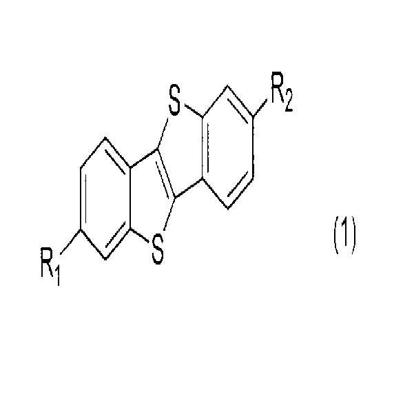
(식 (1) 중, R1 및 R2는 각각 독립적으로 무치환 또는 할로겐 치환 C1-C36 지방족 탄화수소기를 나타냄)(In Formula (1), R 1 and R 2 each independently represent an unsubstituted or halogen-substituted C1-C36 aliphatic hydrocarbon group.)
에 관한 것이다..
상기식 (1)로 나타나는 화합물 및 시아노기를 갖는 전자 수용성 화합물이 적어도 1종류의 유기 용매에 용해 및/또는 분산되어 이루어지는 유기 반도체 재료를 이용하여, 전계 효과 트랜지스터를 형성한 경우에, 높은 캐리어 이동도를 유지하면서, 문턱 전압의 저감 등의 반도체 특성을 개선할 수 있을 뿐만 아니라, 적은 공정으로 균일성이 높은 박막 형성이 가능한 우수한 인쇄 적성을 구비한 실용적인 전계 효과 트랜지스터를 제공할 수 있다. High carrier transfer when a field effect transistor is formed using an organic semiconductor material in which the compound represented by the formula (1) and the electron-accepting compound having a cyano group are dissolved and / or dispersed in at least one organic solvent. It is possible to provide a practical field effect transistor having excellent printing aptitude capable of forming a thin film with high uniformity in a small process as well as improving semiconductor characteristics such as reducing a threshold voltage while maintaining the drawing.
도 1은 본 발명의 전계 효과 트랜지스터의 구조의 일례를 나타내는 개략도이다. 1 is a schematic diagram showing an example of the structure of a field effect transistor of the present invention.
(발명을 실시하기 위한 형태)(Mode for carrying out the invention)
본 발명을 상세하게 설명한다. 본 발명은 특정의 유기 복소환식 화합물 및 시아노기를 갖는 전자 수용성 화합물이 적어도 1종류의 유기 용매에 용해 및/또는 분산되어 이루어지는 유기 반도체 재료 그리고 그들을 이용한 전계 효과 트랜지스터 및 그의 제조 방법에 관한 것이다.The present invention will be described in detail. The present invention relates to an organic semiconductor material in which a specific organic heterocyclic compound and an electron-accepting compound having a cyano group are dissolved and / or dispersed in at least one organic solvent, a field effect transistor using the same, and a manufacturing method thereof.
먼저, 상기식 (1)로 나타나는 화합물에 대해서 설명한다. 상기식 (1) 중, R1 및 R2는 각각 독립적으로 무치환 또는 할로겐 치환 C1-C36 지방족 탄화수소기를 나타낸다. 지방족 탄화수소기는, 포화 또는 불포화의 직쇄, 분기쇄 또는 환상의 지방족 탄화수소기이고, 바람직하게는 직쇄 또는 분기쇄의 지방족 탄화수소기이며, 더욱 바람직하게는 직쇄의 지방족 탄화수소기이다. 탄소수는 통상 C1-C36이고, 바람직하게는 C2-C24, 보다 바람직하게는 C4-C20, 더욱 바람직하게는 C6-C12이다. First, the compound represented by said formula (1) is demonstrated. In said formula (1), R <1> and R <2> respectively independently represents an unsubstituted or halogen substituted C1-C36 aliphatic hydrocarbon group. The aliphatic hydrocarbon group is a saturated or unsaturated linear, branched or cyclic aliphatic hydrocarbon group, preferably a linear or branched aliphatic hydrocarbon group, and more preferably a linear aliphatic hydrocarbon group. Carbon number is C1-C36 normally, Preferably it is C2-C24, More preferably, it is C4-C20, More preferably, it is C6-C12.
직쇄 또는 분기쇄의 포화 지방족 탄화수소기의 구체예로서는, 메틸, 에틸, 프로필, iso-프로필, n-부틸, iso-부틸, t-부틸, n-펜틸, iso-펜틸, t-펜틸, sec-펜틸, n-헥실, iso-헥실, n-헵틸, sec-헵틸, n-옥틸, n-노닐, sec-노닐, n-데실, n-운데실, n-도데실, n-트리데실, n-테트라데실, n-펜타데실, n-헥사데실, n-헵타데실, n-옥타데실, n-노나데실, n-에이코실, 도코실, n-펜타코실, n-옥타코실, n-트리콘틸, 5-(n-펜틸)데실, 헨에이코실, 트리코실, 테트라코실, 헥사코실, 헵타코실, 노나코실, n-트리아콘틸, 스쿠아릴, 도트리아콘틸(dotriacontyl), 헥사트리아콘틸 등을 들 수 있다. 또한, 환상의 포화 지방족 탄화수소기의 구체예로서는, 사이클로헥실, 사이클로펜틸, 아다만틸, 노르보닐 등을 들 수 있다. 직쇄 또는 분기쇄의 불포화 지방족 탄화수소기의 구체예로서는 비닐, 아릴, 에이코사디에닐, 11,14-에이코사디에닐, 게라닐(트랜스-3,7-디메틸-2,6-옥타디엔-1-일), 파르네실(트랜스,트랜스-3,7,11-트리메틸-2,6,10-도데카트리엔-1-일), 4-펜테닐, 1-프로피닐, 1-헥시닐, 1-옥티닐, 1-데시닐, 1-운데시닐, 1-도데시닐, 1-테트라데시닐, 1-헥사데시닐, 1-노나데시닐 등을 들 수 있다. Specific examples of the linear or branched saturated aliphatic hydrocarbon group include methyl, ethyl, propyl, iso-propyl, n-butyl, iso-butyl, t-butyl, n-pentyl, iso-pentyl, t-pentyl, sec-pentyl , n-hexyl, iso-hexyl, n-heptyl, sec-heptyl, n-octyl, n-nonyl, sec-nonyl, n-decyl, n-undecyl, n-dodecyl, n-tridecyl, n- Tetradecyl, n-pentadecyl, n-hexadecyl, n-heptadecyl, n-octadecyl, n-nonadecyl, n-eicosyl, docosyl, n-pentacosyl, n-octacosyl, n-tricontyl , 5- (n-pentyl) decyl, hencosyl, tricosyl, tetracosyl, hexacosyl, heptacosyl, nonacosyl, n-triacyl, squary, dotriacontyl, hexatriac And the like. Moreover, cyclohexyl, cyclopentyl, adamantyl, norbornyl, etc. are mentioned as a specific example of cyclic saturated aliphatic hydrocarbon group. Specific examples of the linear or branched unsaturated aliphatic hydrocarbon group include vinyl, aryl, eicosadienyl, 11,14-eicosadienyl and geranyl (trans-3,7-dimethyl-2,6-octadiene-1- 1), farnesyl (trans, trans-3,7,11-trimethyl-2,6,10-dodecatrien-1-yl), 4-pentenyl, 1-propynyl, 1-hexynyl, 1- Octynyl, 1-decynyl, 1-undecynyl, 1-dodecynyl, 1-tetradecynyl, 1-hexadecynyl, 1-nonadecinyl and the like.
직쇄, 분기쇄 및 환상의 지방족 탄화수소기 중, 직쇄 또는 분기쇄의 지방족 탄화수소기가 바람직하고, 직쇄의 지방족 탄화수소기가 특히 바람직하다. Among the linear, branched and cyclic aliphatic hydrocarbon groups, linear or branched aliphatic hydrocarbon groups are preferable, and linear aliphatic hydrocarbon groups are particularly preferable.
포화 또는 불포화의 지방족 탄화수소기란, 포화의 알킬기, 탄소-탄소 이중 결합을 포함하는 알케닐기 및 탄소-탄소 삼중 결합을 포함하는 알키닐기를 들 수 있고, 보다 바람직하게는 알킬기 또는 알키닐기이며, 더욱 바람직하게는 알킬기이다. 지방족 탄화수소 잔기로서는, 이들 포화 또는 불포화의 지방족 탄화수소기를 조합한 것으로, 즉 지방족 탄화수소기 중의 부위에 탄소-탄소 이중 결합, 탄소-탄소 삼중 결합을 동시에 포함하는 경우도 모두 포함된다. The saturated or unsaturated aliphatic hydrocarbon group includes a saturated alkyl group, an alkenyl group containing a carbon-carbon double bond, and an alkynyl group containing a carbon-carbon triple bond, and more preferably an alkyl group or an alkynyl group, and more preferably. Preferably an alkyl group. Examples of the aliphatic hydrocarbon residue include a combination of these saturated or unsaturated aliphatic hydrocarbon groups, that is, the case where both the carbon-carbon double bond and the carbon-carbon triple bond are contained in the aliphatic hydrocarbon group at the same time.
할로겐 치환 지방족 탄화수소기란, 임의의 종류의 할로겐 원자가 상기의 지방족 탄화수소기의 임의의 위치에 임의의 수로 치환되어 있는 것을 의미한다. 할로겐 원자로서는, 불소 원자, 염소 원자, 브롬 원자, 요오드 원자를 들 수 있고, 바람직하게는 불소 원자, 염소 원자, 브롬 원자, 보다 바람직하게는 불소 원자 및 브롬 원자를 들 수 있다. 할로겐 치환 지방족 탄화수소기의 구체예로서는, 클로로메틸, 브로모메틸, 트리플루오로메틸, 펜타플루오로에틸, n-퍼플루오로프로필, n-퍼플루오로부틸, n-퍼플루오로펜틸, n-퍼플루오로옥틸, n-퍼플루오로데실, n-(도데카플루오로)-6-요오도헥실, 2,2,3,3,3-펜타플루오로프로필, 2,2,3,3-테트라플루오로프로필 등을 들 수 있다. The halogen-substituted aliphatic hydrocarbon group means that any kind of halogen atoms are substituted by any number at any position of the aliphatic hydrocarbon group described above. As a halogen atom, a fluorine atom, a chlorine atom, a bromine atom, and an iodine atom are mentioned, Preferably a fluorine atom, a chlorine atom, a bromine atom, More preferably, a fluorine atom and a bromine atom are mentioned. Specific examples of the halogen-substituted aliphatic hydrocarbon group include chloromethyl, bromomethyl, trifluoromethyl, pentafluoroethyl, n-perfluoropropyl, n-perfluorobutyl, n-perfluoropentyl, and n-purple Urooctyl, n-perfluorodecyl, n- (dodecafluoro) -6-iodohexyl, 2,2,3,3,3-pentafluoropropyl, 2,2,3,3-tetra Fluoropropyl, etc. are mentioned.
상기식 (1)로 나타나는 화합물은, 예를 들면 특허문헌 1 및, 비특허문헌 1에 기재된 공지의 방법에 의해 합성할 수 있다. The compound represented by said formula (1) can be synthesize | combined by the well-known method of patent document 1 and nonpatent literature 1, for example.
상기식 (1)로 나타나는 화합물의 정제 방법은, 특별히 한정되지 않고, 재결정, 칼럼 크로마토그래피 및, 진공 승화 정제 등의 공지의 방법을 채용할 수 있다. 또한 필요에 따라서 이들 방법을 조합하여 이용해도 좋다. The purification method of the compound represented by said Formula (1) is not specifically limited, Well-known methods, such as recrystallization, column chromatography, and a vacuum sublimation purification, can be employ | adopted. Moreover, you may use combining these methods as needed.
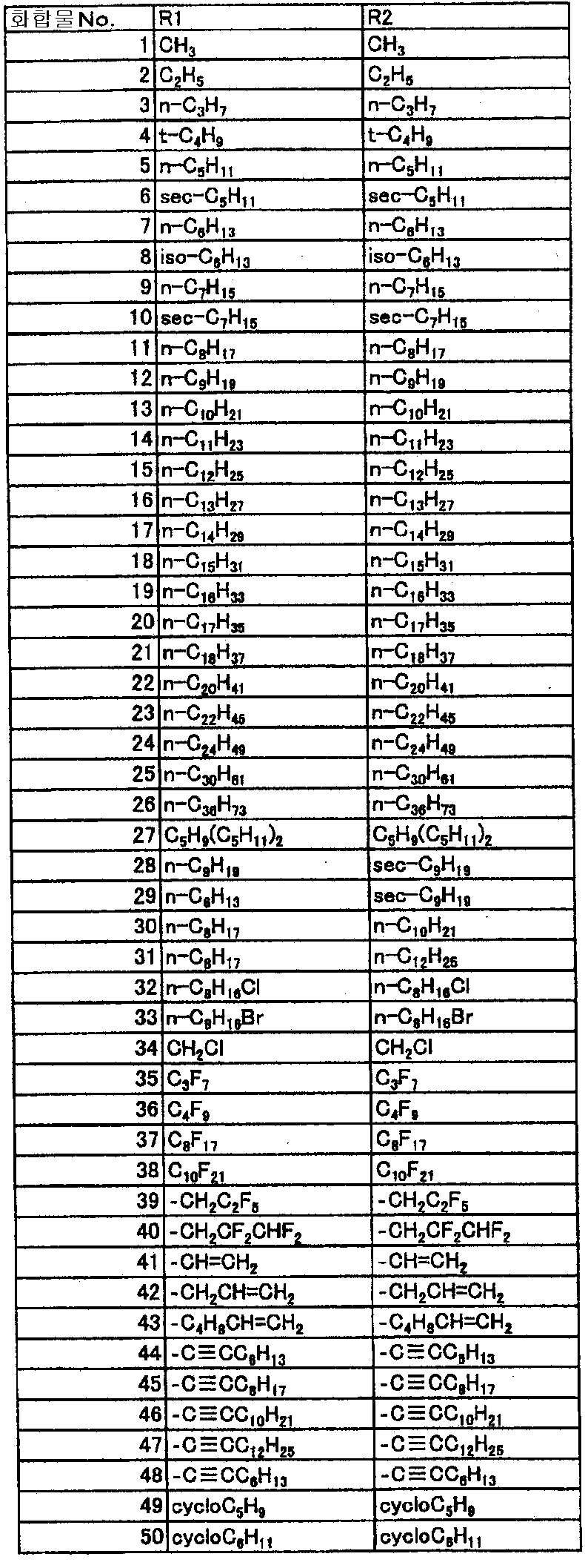
하기표 1에 상기식 (1)로 나타나는 화합물의 구체예를 나타낸다. Specific examples of the compound represented by Formula (1) are shown in Table 1 below.
시아노기를 갖는 전자 수용성 화합물은, 유기 반도체 재료에 도핑하는 첨가물이며, 특별히 한정되지 않지만, 테트라시아노퀴노디메탄(이후 TCNQ로 약기) 또는 그의 유도체를 들 수 있고, 구체적으로는 TCNQ, 2,3,5,6-테트라플루오로테트라시아노-1,4-벤조퀴노디메탄(이후 F4-TCNQ로 약기), 트리플루오로메틸테트라시아노퀴노디메탄(CF3TCNQ), 2,5-디플루오로테트라시아노퀴노디메탄(F2TCNQ), 플루오로테트라시아노퀴노디메탄(FTCNQ), 테트라시아노에틸렌(TCNE), 11,11,12,12-테트라시아노나프토-2,6-퀴노디메탄(TNAP)이나 일본공개특허공보 2008-530773호에 기재된 시아노기를 갖는 퀴노디메탄류가 적합하게 이용된다. 그 중에서도 TCNQ 또는 F4-TCNQ가 특히 바람직하다. The electron-accepting compound having a cyano group is an additive that is doped with an organic semiconductor material, and is not particularly limited. Examples thereof include tetracyanoquinomimethane (hereinafter abbreviated as TCNQ) or a derivative thereof. Specifically, TCNQ, 2, 3,5,6-tetrafluorotetracyano-1,4-benzoquinodimethane (hereinafter abbreviated as F4-TCNQ), trifluoromethyltetracyanoquinodimethane (CF3TCNQ), 2,5-difluoro Lotetracyanoquinomethane (F2TCNQ), Fluorotetracyanoquinomethane (FTCNQ), Tetracyanoethylene (TCNE), 11,11,12,12-tetracyanonaphtho-2,6-quinodi Methane (TNAP) and quinodimethanes having cyano groups described in JP-A-2008-530773 are suitably used. Especially, TCNQ or F4-TCNQ is especially preferable.
본 발명의 유기 반도체 재료는, 적어도 상기식 (1)로 나타나는 화합물 및 시아노기를 갖는 전자 수용성 화합물을 유기 용매에 용해 또는 분산되어 이루어지는 것이지만, 상기식 (1)로 나타나는 화합물 및 시아노기를 갖는 전자 수용성 화합물을 1종류씩 함유해도, 상기식 (1)로 나타나는 화합물 및 시아노기를 갖는 전자 수용성 화합물의 한쪽 또는 양쪽 모두의 수 종류의 유도체를 혼합하여 이용해도 좋다. 상기식 (1)로 나타나는 화합물과 시아노기를 갖는 전자 수용성 화합물을 포함하는 유기 반도체 재료 중에 있어서, 상기식 (1)로 나타나는 화합물에 대한 시아노기를 갖는 전자 수용성 화합물의 함유율은 통상 0.1?40질량%의 범위이지만, 0.1?20질량%인 것이 바람직하고, 0.1?10질량%인 것이 보다 바람직하다. 함유율이 40질량%를 초과하면 OFF 전류의 증가에 의해 특성값이 저하해 버린다. TCNQ 또는 F4-TCNQ를 이용하는 경우, 함유율은 10질량% 이하인 것이 특히 바람직하다. The organic semiconductor material of the present invention is formed by dissolving or dispersing at least the compound represented by the formula (1) and the electron-accepting compound having a cyano group in an organic solvent, but the electron having the compound represented by the formula (1) and the cyano group Even if it contains one type of water-soluble compound, you may mix and use the several types of derivatives of one or both of the compound represented by said Formula (1), and the electron-accepting compound which has a cyano group. In the organic-semiconductor material containing the compound represented by said Formula (1), and the electron-accepting compound which has a cyano group, the content rate of the electron-accepting compound which has a cyano group with respect to the compound represented by said Formula (1) is 0.1-40 mass normally. Although it is the range of%, it is preferable that it is 0.1-20 mass%, and it is more preferable that it is 0.1-10 mass%. When content rate exceeds 40 mass%, a characteristic value will fall by increase of OFF current. When using TCNQ or F4-TCNQ, it is especially preferable that content rate is 10 mass% or less.
본 발명의 유기 반도체 재료에는, 본 발명의 효과를 손상시키지 않는 한, 전계 효과 트랜지스터의 특성의 개선이나 기타 특성을 부여하기 위해 필요에 따라서 기타 유기 반도체 재료나 각종 첨가제를 혼합해도 좋다. 이들 첨가제로서는, 점도 조정제, 표면 장력 조정제, 레벨링제, 침투제, 레올로지 조정제, 배향제, 분산제 등을 들 수 있다. Other organic semiconductor materials and various additives may be mixed with the organic semiconductor material of the present invention as necessary in order to improve the characteristics of the field effect transistor or to impart other characteristics as long as the effects of the present invention are not impaired. As these additives, a viscosity regulator, a surface tension regulator, a leveling agent, a penetrant, a rheology regulator, an aligning agent, a dispersing agent, etc. are mentioned.
이들 첨가제의 함유율은, 본 발명의 유기 반도체 재료의 총량에 대하여 0?30질량%이며, 0?20질량%가 바람직하고, 0?10질량%가 보다 바람직하다. The content rate of these additives is 0-30 mass% with respect to the total amount of the organic-semiconductor material of this invention, 0-20 mass% is preferable, and 0-10 mass% is more preferable.
본 발명의 유기 반도체 재료는, 식 (1)로 나타나는 화합물 및 전자 수용성 화합물을 용매에 용해 또는 분산되어 유기 반도체 재료의 도포 인쇄 프로세스 적응성을 향상시킨 것이다. 사용할 수 있는 용매로서는 화합물을 기판 상에 성막할 수 있으면 특별히 한정되는 것은 아니지만, 유기 용매가 바람직하고, 단일의 유기 용매로도, 복수의 유기 용매를 혼합하여 사용할 수도 있다. 구체적으로는 클로로포름, 염화 메틸렌, 디클로로에탄 등의 할로겐 탄화수소계 용매; 메탄올, 에탄올, 이소프로필알코올, 부탄올 등의 알코올계 용매; 옥타플루오로펜탄올, 펜타플루오로프로판올 등의 불화 알코올계 용매; 아세트산 에틸, 아세트산 부틸, 벤조산 에틸, 탄산 디에틸 등의 에스테르계 용매; 톨루엔, 자일렌, 벤젠, 클로로벤젠, 메시틸렌, 에틸벤젠, 디에틸벤젠, 트리에틸벤젠, 디클로로벤젠, 클로로나프탈렌, 테트라하이드로나프탈렌, 데칼린, 사이클로헥실벤젠 등의 방향족 탄화수소계 용매; 아세톤, 메틸에틸케톤, 메틸이소부틸케톤, 사이클로펜탄온, 사이클로헥사논 등의 케톤계 용매; 디메틸포름아미드, 디메틸아세트아미드, N-메틸피롤리돈 등의 아미드계 용매; 테트라하이드로푸란, 디이소부틸에테르 등의 에테르계 용매; 헥산, 사이클로헥산, 옥탄, 데칸, 테트라인 등의 탄화수소계 용매; 아세토니트릴, 프로피오노니트릴, 부티로니트릴, 벤조니트릴 등의 니트릴계 용매 등을 이용할 수 있고, 이들은 단독으로도, 혼합하여 사용할 수도 있다. 식 (1)로 나타나는 화합물 및 전자 수용성 화합물의 농도는, 용매의 종류나, 제작하는 반도체층의 막두께에 따라 상이하지만, 혼합액 중의 용매에 대하여 총량으로 0.001?50질량%이며, 0.01?20질량%인 것이 바람직하다. 또한, 본 발명의 반도체 재료는 상기의 유기 용매에 용해 또는 분산되어 있으면 좋지만, 보다 균일한 박막을 형성하는데에 있어서는, 균일한 용액으로서 용해되어 있는 쪽이 바람직하다. The organic-semiconductor material of this invention melt | dissolves or disperse | distributes the compound and electron-accepting compound represented by Formula (1) in the solvent, and improved the application | coating printing process adaptability of an organic semiconductor material. As a solvent which can be used, if a compound can be formed into a film on a board | substrate, it will not specifically limit, but an organic solvent is preferable and even a single organic solvent can mix and use a some organic solvent. Specifically, Halogen hydrocarbon solvent, such as chloroform, methylene chloride, dichloroethane; Alcohol solvents such as methanol, ethanol, isopropyl alcohol and butanol; Fluorinated alcohol solvents such as octafluoropentanol and pentafluoropropanol; Ester solvents such as ethyl acetate, butyl acetate, ethyl benzoate and diethyl carbonate; Aromatic hydrocarbon solvents such as toluene, xylene, benzene, chlorobenzene, mesitylene, ethylbenzene, diethylbenzene, triethylbenzene, dichlorobenzene, chloronaphthalene, tetrahydronaphthalene, decalin and cyclohexylbenzene; Ketone solvents such as acetone, methyl ethyl ketone, methyl isobutyl ketone, cyclopentanone and cyclohexanone; Amide solvents such as dimethylformamide, dimethylacetamide and N-methylpyrrolidone; Ether solvents such as tetrahydrofuran and diisobutyl ether; Hydrocarbon solvents such as hexane, cyclohexane, octane, decane and tetraine; Nitrile solvents, such as acetonitrile, propiononitrile, butyronitrile, and benzonitrile, etc. can be used, These can also be used individually or in mixture. Although the density | concentration of the compound and electron-accepting compound represented by Formula (1) changes with kinds of solvent and the film thickness of the semiconductor layer to produce, it is 0.001-50 mass% in total amount with respect to the solvent in a liquid mixture, 0.01-20 mass It is preferable that it is%. In addition, although the semiconductor material of this invention should just melt | dissolve or disperse | distribute in said organic solvent, In order to form a more uniform thin film, it is more preferable to melt | dissolve as a uniform solution.
본 발명의 전계 효과 트랜지스터(Field effect transistor, 이하 FET로 약기하는 경우가 있음)는, 반도체층에 접하여 소스 전극 및 드레인 전극의 2개의 전극이 있고, 그 2개의 전극 간에 흐르는 전류를, 게이트 절연체층을 개재하여 게이트 전극으로 불리는 다른 하나의 전극에 인가하는 전압으로 제어하는 것이다. 전계 효과 트랜지스터는 상기 유기 박막을 포함하고 있다. A field effect transistor (hereinafter abbreviated as FET) of the present invention has two electrodes, that is, a source electrode and a drain electrode, in contact with the semiconductor layer, and current flowing between the two electrodes is applied to the gate insulator layer To a voltage to be applied to the other electrode called a gate electrode. The field effect transistor includes the organic thin film.
도 1에 본 발명의 전계 효과 트랜지스터의 몇 가지의 태양을 나타내지만, 각 층이나 전극의 배치는, 소자의 용도에 의해 적절히 선택할 수 있다. 또한, 도 1에 있어서 동일한 명칭에는 동일한 번호를 붙이는 것으로 한다. Although some aspects of the field effect transistor of this invention are shown in FIG. 1, the arrangement | positioning of each layer and electrode can be suitably selected by the use of an element. In addition, the same number is attached | subjected to the same name in FIG.
다음으로 도 1에 나타내는 본 발명의 전계 효과 트랜지스터의 각 구성 요소에 대해서 설명하지만, 이에 한정되지 않는다. Next, although each component of the field effect transistor of this invention shown in FIG. 1 is demonstrated, it is not limited to this.
기판(1)은, 그 위에 형성되는 각 층이 박리되는 일 없이 보존유지할 수 있는 것이 필요하다. 예를 들면, 수지판, 수지 필름, 종이, 유리, 석영, 세라믹 등의 절연성 재료; 금속 또는 합금 등의 도전성 기판 상에 절연층을 코팅한 형성물; 수지와 무기 재료 등과의 각종 조합으로 이루어지는 재료 등을 사용할 수 있다. 그 중에서도 일반적으로 사용되는 수지 필름으로서는, 예를 들면, 폴리에틸렌테레프탈레이트, 폴리에틸렌나프탈레이트, 폴리에테르술폰, 폴리아미드, 폴리이미드, 폴리카보네이트, 셀룰로오스트리아세테이트, 폴리에테르이미드 등을 들 수 있다. 수지 필름 또는 종이를 이용하면, 반도체 소자에 가효성을 갖게할 수 있어, 플렉시블하고 경량이 되어, 실용성이 향상된다. 기판의 두께는, 통상 1㎛?10㎜이며, 바람직하게는 5㎛?3㎜이다. The board | substrate 1 needs to be able to hold | maintain without peeling each layer formed on it. For example, insulating materials, such as a resin plate, a resin film, paper, glass, quartz, a ceramic; A formation in which an insulating layer is coated on a conductive substrate such as a metal or an alloy; The material etc. which consist of various combinations of resin, an inorganic material, etc. can be used. Especially, as a resin film generally used, polyethylene terephthalate, polyethylene naphthalate, polyether sulfone, polyamide, polyimide, polycarbonate, cellulose triacetate, polyetherimide, etc. are mentioned, for example. When a resin film or paper is used, the semiconductor element can be made effective, and it becomes flexible and lightweight, and the practicality is improved. The thickness of a board | substrate is 1 micrometer-10 mm normally, Preferably they are 5 micrometers-3 mm.
소스 전극(2), 드레인 전극(3), 게이트 전극(6)에는 도전성을 갖는 재료가 이용된다. 예를 들면, 백금, 금, 은, 알루미늄, 크롬, 텅스텐, 탄탈, 니켈, 코발트, 구리, 철, 연, 주석, 티탄, 인듐, 팔라듐, 몰리브덴, 마그네슘, 칼슘, 바륨, 리튬, 칼륨, 나트륨 등의 금속 및 그들을 포함하는 합금; InO2, ZnO2, SnO2, ITO 등의 도전성 산화물; 폴리아닐린, 폴리피롤, 폴리티오펜(PEDOTㆍPSS 등), 폴리아세틸렌, 폴리파라페닐렌비닐렌, 폴리디아세틸렌 등의 도전성 고분자 화합물; BED-TTF 등의 유기 전하 이동 착체; 실리콘, 게르마늄, 갈륨 비소 등의 반도체; 카본 블랙, 풀러렌(fullerene), 카본나노튜브, 그래파이트 등의 탄소 재료 등을 사용할 수 있다. 또한, 도전성 고분자 화합물이나 반도체에는 도핑을 행해도 좋고, 도펀트로서는, 예를 들면, 염산, 황산, 술폰산 등의 산; PF5, AsF5, FeCl3 등의 루이스산; 요오드 등의 할로겐 원자, 리튬, 나트륨, 칼륨 등의 금속 원자 등이 이용된다. 전극의 접촉 저항을 저하시키기 위해 산화 몰리브덴을 도핑하는 방법이나 금속에 티올 등의 처리를해도 좋다. 또한, 상기 재료에 카본 블랙이나 금, 백금, 은, 구리 등의 금속 입자를 분산한 도전성의 복합재료도 이용된다. 각 전극(2, 3, 6)에는 배선이 연결되지만, 배선도 전극과 거의 동일한 재료로 제작된다. 소스 전극(2), 드레인 전극(3), 게이트 전극(6)의 막두께는, 재료에 따라 상이하지만, 통상 0.1㎚?100㎛이고, 바람직하게는 0.5㎚?10㎛이며, 보다 바람직하게는 1㎚?5㎛이다. A conductive material is used for the
게이트 절연체층(5)은 절연성을 갖는 재료이며, 예를 들면, 폴리파라자일렌, 폴리아크릴레이트, 폴리메틸메타크릴레이트, 폴리스티렌, 폴리비닐페놀, 폴리아미드, 폴리이미드, 폴리카보네이트, 폴리에스테르, 폴리비닐알코올, 폴리아세트산 비닐, 폴리우레탄, 폴리술폰, 에폭시 수지, 페놀 수지 등의 폴리머 및 이들을 조합한 공중합체; 이산화 규소, 산화 알류미늄, 산화 티탄, 산화 탄탈 등의 산화물; SrTiO3, BaTiO3 등의 강(强)유전성 산화물; 질화 규소, 질화 알루미늄 등의 질화물; 황화물; 불화물 등의 유전체, 혹은 이들 유전체의 입자를 분산시킨 폴리머 등을 사용할 수 있다. 게이트 절연체층(5)의 막두께는, 재료에 따라 상이하지만, 통상 0.1㎚?100㎛, 바람직하게는 0.5㎚?50㎛, 보다 바람직하게는 5㎚?10㎛이다. The gate insulator layer 5 is an insulating material, and for example, polyparaxylene, polyacrylate, polymethylmethacrylate, polystyrene, polyvinylphenol, polyamide, polyimide, polycarbonate, polyester, Polymers such as polyvinyl alcohol, polyvinyl acetate, polyurethane, polysulfone, epoxy resin, phenol resin, and copolymers thereof; Oxides such as silicon dioxide, aluminum oxide, titanium oxide and tantalum oxide; SrTiO 3 , BaTiO 3 Ferroelectric oxides such as these; Nitrides such as silicon nitride and aluminum nitride; sulfide; Dielectrics, such as a fluoride, or the polymer which disperse | distributed the particle | grains of these dielectrics, etc. can be used. Although the film thickness of the gate insulator layer 5 changes with materials, it is 0.1 nm-100 micrometers normally, Preferably it is 0.5 nm-50 micrometers, More preferably, it is 5 nm-10 micrometers.
반도체층(4)에 포함되는 유기 반도체 재료는, 적어도 상기식 (1) 및 시아노기를 갖는 전자 수용성 화합물로 이루어지지만, 각각의 유도체를 수 종류씩 혼합하여 이용해도 좋고, 당해 반도체 재료를 총량에 대하여 50질량% 이상, 바람직하게는 80질량% 이상, 보다 바람직하게는 95질량% 이상 포함하는 것이 필요하다. 이때, 전계 효과 트랜지스터의 특성 개선이나 기타 특성을 부여하기 위해, 필요에 따라서 기타 유기 반도체 재료나 각종 첨가제를 혼합해도 좋다. 또한 반도체층(4)은 복수의 층으로 이루어져 있어도 좋다. 반도체층(4)의 막두께는, 필요한 기능을 잃지 않는 범위에서, 얇을수록 바람직하다. 전계 효과 트랜지스터에 있어서는, 소정 이상의 막두께가 있으면 반도체 소자의 특성은 막두께에 의존하지 않지만, 막두께가 두꺼워지면 누설 전류가 증가하는 경우가 많다. 반대로 너무 얇으면 전하가 통로(채널)를 형성할 수 없게 되기 때문에, 적절한 막두께는 필요하다. 반도체가 필요한 기능을 나타내기 위한 반도체층의 막두께는, 통상, 0.1㎚?10㎛, 바람직하게는 0.5㎚?5㎛, 보다 바람직하게는 1㎚?3㎛이다. Although the organic-semiconductor material contained in the
보호층(7)의 재료로서는 특별히 한정되지 않지만, 예를 들면, 에폭시 수지, 폴리메틸메타크릴레이트 등의 아크릴 수지, 폴리우레탄, 폴리이미드, 폴리비닐알코올, 불소 수지, 폴리올레핀 등의 각종 수지로 이루어지는 막이나, 산화 규소, 산화 알류미늄, 질화 규소 등 , 무기 산화막이나 질화막 등의 유전체로 이루어지는 막이 바람직하게 이용되며, 특히, 산소 투과율이나 흡수율의 낮은 수지(폴리머)가 바람직하다. 또한, 유기 EL 디스플레이용으로 개발되고 있는 보호 재료도 사용이 가능하다. 보호층의 막두께는, 그 목적에 따라서 임의의 막두께를 채용할 수 있지만, 통상 100㎚?1㎜이다. 보호층을 형성하면, 습도 등의 외기(外氣)의 영향을 작게 할 수 있고, 또한, 디바이스의 ON/OFF비를 올릴 수 있는 등, 전기적 특성 안정화의 이점도 있다. Although it does not specifically limit as a material of the
본 발명의 전계 효과 트랜지스터는, 기판 표면의 세정 처리로서 염산이나 황산, 아세트산 등에 의한 산 처리, 수산화 나트륨, 수산화 칼륨, 수산화 칼슘, 암모니아 등에 의한 알칼리 처리, 오존 처리, 불소화 처리, 산소나 아르곤 등의 플라즈마 처리, 랭뮤어ㆍ블로젯막의 형성 처리, 그 외의 절연체나 반도체의 박막의 형성 처리, 기계적 처리, 코로나 방전 등의 전기적 처리 등을 행함으로써 우수한 인쇄 적정을 나타낼 수 있지만, 그 외에, 상기한 각 층의 사이나, 반도체 소자의 외면에 필요에 따라서 기타 층을 형성해도 좋다. 또한 반도체층이 적층되는 기판이나 절연체층 상 등에 미리 표면 처리를 행함으로써, 기판, 전극 등과 그 후에 성막되는 반도체층과의 계면 부분의 분자 배향이나 결정성의 제어, 전극 계면이나 절연체층 상의 트랩 부위의 저감에 의해 캐리어 이동도 등의 특성을 개량하거나, 기판 표면의 친수성/소수성의 밸런스를 조정함으로써, 그 위에 성막되는 막의 막질이나 기판으로의 도포성의 개량에 의해 디바이스의 균일성을 더욱 향상시키는 것이 가능하다. 이러한 기판 처리로서는, 예를 들면, 페닐에틸트리클로로실란 등에 의한 실란커플링 처리, 티올 처리나 섬유 등을 이용한 러빙 처리 등을 들 수 있다. The field effect transistor of the present invention may be treated with an acid treatment with hydrochloric acid, sulfuric acid, acetic acid or the like, alkali treatment with sodium hydroxide, potassium hydroxide, calcium hydroxide, ammonia, ozone treatment, fluorination treatment, oxygen or argon, etc. Excellent printing titration can be obtained by performing plasma treatment, Langmuir-Blodgett film formation treatment, other insulator or semiconductor thin film formation treatment, mechanical treatment, electrical treatment such as corona discharge, and the like. Other layers may be formed between the layers or on the outer surface of the semiconductor element as necessary. In addition, the surface treatment is performed on a substrate or an insulator layer on which a semiconductor layer is laminated in advance, thereby controlling molecular orientation and crystallinity of an interface portion with a substrate, an electrode, or the like, and then depositing a film. By improving the characteristics such as carrier mobility by reducing or adjusting the hydrophilicity / hydrophobicity of the surface of the substrate, it is possible to further improve the uniformity of the device by improving the film quality of the film formed thereon or the coating property on the substrate. Do. As such a substrate process, the silane coupling process by phenyl ethyl trichlorosilane etc., the rubbing process using a thiol process, a fiber, etc. are mentioned, for example.
본 발명에 있어서 각 층을 형성하는 방법으로서는, 예를 들면, 진공 증착법, 스퍼터법, 도포법, 인쇄법, 졸겔법 등이 적절히 사용할 수 있지만, 생산성을 고려하면, 도포법이나 잉크젯 인쇄 등의 인쇄법이 바람직하다. As the method for forming each layer in the present invention, for example, a vacuum deposition method, a sputtering method, a coating method, a printing method, a sol-gel method and the like can be appropriately used. The law is preferred.
다음으로, 본 발명의 전계 효과 트랜지스터의 제조 방법에 대해서, 도 1의 태양예에 기초하여 이하에 설명한다. Next, the manufacturing method of the field effect transistor of this invention is demonstrated below based on the example of FIG.
(기판 및 기판 처리)(Substrate and substrate processing)
본 발명의 전계 효과 트랜지스터는, 상기의 기판(1) 상에 필요한 전극이나 각종의 층을 형성함으로써 제작된다(도 1 참조). 이 기판 상에는 전술의 표면 처리 등을 행하는 것도 가능하다. 기판(1)의 두께는, 필요한 기능을 방해하지 않는 범위에서 얇은 쪽이 바람직하다. 재료에 따라서도 상이하지만, 통상 1㎛?10㎜이며, 바람직하게는 5㎛?3㎜이다. The field effect transistor of the present invention is produced by forming necessary electrodes and various layers on the substrate 1 (see FIG. 1). It is also possible to perform the above-mentioned surface treatment on this board | substrate. It is preferable that the thickness of the board | substrate 1 is thin in the range which does not prevent a required function. Although it changes also with a material, it is 1 micrometer-10 mm normally, Preferably it is 5 micrometers-3 mm.
(소스 전극 및 드레인 전극의 형성)(Formation of source electrode and drain electrode)
상기의 전극 재료 등을 이용하여 기판(1) 상에 소스 전극(2) 및 드레인 전극(3)을 형성한다. 소스 전극(2) 및 드레인 전극(3)의 재료는 동일해도, 상이해도 좋다. 전극을 형성하는 방법으로서는, 예를 들면 진공 증착법, 스퍼터법, 도포법, 열전사법, 인쇄법, 졸겔법 등을 들 수 있다. 성막시 또는 성막 후, 소망하는 형상이 되도록 필요에 따라서 패터닝을 행하는 것이 바람직하다. 패터닝의 방법으로서도 각종의 방법을 사용할 수 있지만, 예를 들면 포토 레지스트의 패터닝과 에칭을 조합한 포토리소그래피법 등을 들 수 있다. 또한, 잉크젯 인쇄, 스크린 인쇄, 오프셋 인쇄, 볼록판 인쇄 등의 인쇄법, 마이크로콘택트 프린팅법 등의 소프트리소그래피법 및, 이들 수법을 복수 조합한 수법을 이용하여, 패터닝하는 것도 가능하다. 소스 전극(2) 및 드레인 전극(3)의 막두께는, 재료에 따라서도 상이하지만, 통상 0.1㎚?100㎛이고, 바람직하게는 0.5㎚?10㎛이며, 보다 바람직하게는 1㎚?5㎛이다. 소스 전극(2) 및 드레인 전극(3)의 막두께는 동일해도 좋고, 상이해도 좋다. The
(반도체층의 형성)(Formation of Semiconductor Layer)
반도체층은 상기에서 설명한 유기 반도체 재료를 이용하여 도포 인쇄 프로세스에 의해 성막된 유기 박막이다. 유기 박막을 유기 반도체 박막이라고 바꾸어 말할 수도 있다. 도포 인쇄 프로세스란, 용매 가용성을 갖는 유기 반도체 재료, 예를 들면 본 발명의 상기식 (1)로 나타나는 화합물 및 시아노기를 갖는 전자 수용성 화합물을 미리 유기 용매에 용해 또는 분산되어, 얻어진 유기 반도체 재료의 용해액을 도포 또는 인쇄하고, 건조하여 우수한 반도체 특성을 갖는 반도체층을 용이하게 형성할 수 있는 반도체층의 제작 방법을 말한다. 도포 또는 인쇄에 의한 제조 방법, 즉 도포 인쇄 프로세스는 디바이스 제조시의 환경을 진공이나 고온 상태로 할 필요가 없고, 대면적의 전계 효과 트랜지스터를 저비용으로 제조할 수 있기 때문에 공업적으로도 유리하여, 각종 반도체층의 제작 방법 중에서도 특히 바람직하다. The semiconductor layer is an organic thin film formed by a coating printing process using the organic semiconductor material described above. The organic thin film may be referred to as an organic semiconductor thin film. The coating printing process is an organic semiconductor material obtained by dissolving or dispersing an organic semiconductor material having solvent solubility, for example, the compound represented by the formula (1) of the present invention and an electron-accepting compound having a cyano group in an organic solvent in advance. The manufacturing method of the semiconductor layer which can apply | coat or print a melt, dry, and can easily form the semiconductor layer which has the outstanding semiconductor characteristic. The manufacturing method by coating or printing, i.e., the coating printing process, is industrially advantageous because it is not necessary to make the environment at the time of device manufacture in a vacuum or a high temperature state, and a large-area field effect transistor can be manufactured at low cost. It is especially preferable among the manufacturing methods of various semiconductor layers.
구체적으로는, 상기식 (1)로 나타나는 화합물 및 시아노기를 갖는 전자 수용성 화합물을 용매에 용해, 또는 분산함으로써 본 발명의 유기 반도체 재료를 조제한다. 식 (1)로 나타나는 화합물 및 시아노기를 갖는 전자 수용성 화합물은 동시에 용해, 또는 분산화하거나, 개별적으로 용매에 용해 또는 분산한 후에 혼합하여 조제해도 좋다. 본 발명의 유기 반도체 재료 중에 있어서의 식 (1)로 나타나는 화합물 및 시아노기를 갖는 전자 수용성 화합물의 농도(이들 화합물을 각각 복수 종류 사용한 경우는, 복수 종류의 화합물의 총 농도)는, 용매의 종류나, 제작하는 반도체층의 막두께에 따라 상이하지만, 용액 총량에 대하여 통상 0.001?50질량%이고, 0.01?20질량%인 것이 바람직하다. 반도체층의 성막성의 향상이나 전계 효과 트랜지스터 특성의 개선, 기타 특성을 부여하기 위해 첨가제나 타종의 반도체 재료를 혼합하는 것도 가능하다. Specifically, the organic semiconductor material of the present invention is prepared by dissolving or dispersing the compound represented by the formula (1) and the electron-accepting compound having a cyano group in a solvent. The compound represented by the formula (1) and the electron-accepting compound having a cyano group may be dissolved or dispersed at the same time, or separately mixed or dissolved in a solvent before being mixed. The concentration of the compound represented by Formula (1) in the organic semiconductor material of the present invention and the electron-accepting compound having a cyano group (when plural kinds of these compounds are used, respectively, the total concentration of plural kinds of compounds) is a kind of solvent. In addition, although it changes with the film thickness of the semiconductor layer to manufacture, it is preferable that it is 0.001-50 mass% normally with respect to a solution total amount, and it is preferable that it is 0.01-20 mass%. In order to improve the film-forming properties of the semiconductor layer, to improve the field effect transistor characteristics, and to impart other properties, it is also possible to mix additives or other semiconductor materials.
유기 반도체 재료를 조제하려면, 상기식 (1)로 나타나는 화합물 및 시아노기를 갖는 전자 수용성 화합물을 용매에 용해, 또는 분산할 필요가 있지만, 경우에 따라 가열 용해 처리를 행해도 좋다. 또한 얻어진 유기 반도체 재료를 필터를 이용해 여과하여, 불순물 등을 제거해도 좋다. 이를 기판 상에 도포하면, 반도체층의 성막성의 향상을 볼 수 있어, 적합하게 사용할 수 있다. To prepare an organic semiconductor material, it is necessary to dissolve or disperse the compound represented by the formula (1) and the electron-accepting compound having a cyano group in a solvent. In addition, the obtained organic semiconductor material may be filtered using a filter to remove impurities and the like. When this is applied onto a substrate, improvement in the film-forming properties of the semiconductor layer can be seen and can be suitably used.
상기와 같이 조제한 유기 반도체 재료를, 기판(소스 전극 및 드레인 전극의 노출부)에 도포한다. 도포법으로서는, 캐스팅, 스핀 코팅, 딥 코팅, 블레이드 코팅, 와이어 바 코팅, 스프레이 코팅 등의 코팅법; 잉크젯 인쇄, 스크린 인쇄, 오프셋 인쇄, 볼록판 인쇄, 그라비어 인쇄 등의 인쇄법; 마이크로콘택트 프린팅법 등의 소프트리소그래피법 등, 나아가서는 이들 수법을 복수 조합한 방법을 채용할 수 있다. 또한, 도포법에 유사한 방법으로서 수면 상에 상기의 유기 반도체 재료를 적하함으로써 제작한 반도체층의 단분자막을 기판에 옮겨 적층하는 랭뮤어ㆍ블로젯법, 액정이나 융액 상태의 재료를 2매의 기판으로 끼워 모관(毛管) 현상으로 기판 간에 도입하는 방법 등도 채용할 수 있다. 이들 방법에 의해 제작되는 반도체층의 막두께는, 기능을 손상시키지 않는 범위에서 얇은 쪽이 바람직하다. 막두께가 커지면 누설 전류가 증대하는 경우가 있다. 반도체층의 막두께는, 상기의 반도체층(4)과 동일하다. The organic semiconductor material prepared as mentioned above is apply | coated to the board | substrate (exposed part of a source electrode and a drain electrode). Examples of the coating method include coating methods such as casting, spin coating, dip coating, blade coating, wire bar coating, and spray coating; Printing methods such as inkjet printing, screen printing, offset printing, convex printing and gravure printing; Soft lithography such as microcontact printing and the like, and further, a combination of a plurality of these techniques can be employed. In addition, as a method similar to the coating method, the Langmuir-Blodgett method, in which the monolayer film of the semiconductor layer produced by dropping the above organic semiconductor material on the water surface, is laminated on a substrate, and a liquid crystal or a melted material is sandwiched between two substrates. The method which introduce | transduces between board | substrates by a capillary phenomenon etc. can also be employ | adopted. As for the film thickness of the semiconductor layer produced by these methods, the thinner side is preferable in the range which does not impair a function. As the film thickness increases, the leakage current may increase. The film thickness of a semiconductor layer is the same as that of the said
이와 같이 제작된 반도체층은, 후처리에 의해 반도체 특성을 개량할 수 있다. 예를 들면, 반도체층을 형성한 후에 기판을 열처리함으로써, 성막시에 발생한 막 중의 뒤틀림이 완화되어, 막 중의 배열ㆍ배향을 제어할 수 있는 등의 이유에 의해, 반도체 특성의 향상이나 안정화를 도모할 수 있어, 핀홀 등도 저감할 수 있다. 열처리는 반도체층이 형성되어 있으면 어느 단계에서 행해도 좋다. 열처리의 온도는 특별히 제한은 없지만, 통상 실온?150℃에서, 바람직하게는 40?120℃, 더욱 바람직하게는 45?100℃이다. 열처리의 시간은, 특별히 제한은 없지만, 통상 1초?24시간, 바람직하게는 1분?1시간이다. 열처리시의 분위기는 대기 중에서도 좋지만, 질소나 아르곤 등의 불활성 분위기하에서도 좋다. The semiconductor layer thus produced can improve semiconductor characteristics by post-treatment. For example, by forming a semiconductor layer and then heat-treating the substrate, distortion in the film generated during film formation is alleviated, and the improvement and stabilization of semiconductor characteristics can be achieved for reasons such as control of arrangement and orientation in the film. The pinhole etc. can also be reduced. The heat treatment may be performed at any stage as long as the semiconductor layer is formed. Although the temperature of heat processing does not have a restriction | limiting in particular, Usually, at room temperature-150 degreeC, Preferably it is 40-120 degreeC, More preferably, it is 45-100 degreeC. The time for heat treatment is not particularly limited, but is usually 1 second to 24 hours, preferably 1 minute to 1 hour. Although the atmosphere at the time of heat processing may be in air | atmosphere, it is good also in inert atmosphere, such as nitrogen and argon.
(게이트 절연체층의 형성)(Formation of Gate Insulator Layer)
상기의 절연체 재료 등을 이용하여 반도체층(4) 상에 게이트 절연체층(5)을 형성한다(도 1 참조). 게이트 절연체층(5)의 형성 방법으로서는, 예를 들면 스핀 코팅, 스프레이 코팅, 딥 코팅, 캐스팅, 바 코팅, 블레이드 코팅 등의 도포법; 스크린 인쇄, 오프셋 인쇄, 잉크젯 등의 인쇄법; 진공 증착법, 분자선 에피택셜(epitaxial) 성장법, 이온 클러스터 빔법, 이온 플레이팅법, 스퍼터링법, 대기압 플라즈마법, CVD법 등의 드라이 프로세스법 등을 들 수 있다. 또한, 졸겔법이나 알루미늄 상의 알루마이트와 같이 금속 표면에 산화물막을 형성하는 방법도 사용할 수 있다. The gate insulator layer 5 is formed on the
게이트 절연체층(5)의 막두께는, 그 기능을 손상시키지 않는 범위에서 얇은 쪽이 바람직하고, 통상 0.1㎚?100㎛이고, 바람직하게는 0.5㎚?50㎛이며, 보다 바람직하게는 5㎚?10㎛이다. As for the film thickness of the gate insulator layer 5, the thinner is preferable in the range which does not impair the function, It is 0.1 nm-100 micrometers normally, Preferably it is 0.5 nm-50 micrometers, More preferably, it is 5 nm? 10 micrometers.
(게이트 전극의 형성)(Formation of gate electrode)
게이트 전극(6)은, 소스 전극(2) 및 드레인 전극(3)의 작성 방법과 동일한 방법으로 형성할 수 있다. 막두께는, 재료에 따라서도 상이하지만, 통상 1㎚?100㎛이고, 바람직하게는 0.5㎚?10㎛이며, 보다 바람직하게는 1㎚?5㎛이다. The gate electrode 6 can be formed by the same method as the preparation method of the
(보호층)(Protective layer)
상기의 보호층 재료를 사용하여 보호층(7)을 형성하면, 외기의 영향을 최소한으로 할 수 있어, 전계 효과 트랜지스터의 전기적 특성을 안정화할 수 있다는 이점이 있다(도 1 참조). 보호층(7)의 막두께는, 그 목적에 따라서 임의의 막두께를 채용할 수 있지만, 통상 100㎚?1㎜이다. 보호층을 성막하려면 각종의 방법을 채용할 수 있지만, 보호층이 수지로 이루어지는 경우는, 예를 들면, 수지를 함유하는 용액을 도포 후에 건조시켜 수지막으로 하는 방법, 수지 모노머를 도포 혹은 증착한 후에 중합하는 방법 등을 들 수 있고, 성막 후에 가교 처리를 행해도 좋다. 보호층이 무기물로 이루어지는 경우는, 예를 들면, 스퍼터링법, 증착법 등의 진공 프로세스에서의 형성 방법이나, 졸겔법 등의 도포 인쇄 프로세스에서의 형성 방법을 이용할 수 있다. 본 발명의 전계 효과 트랜지스터는, 보호층을 반도체층 표면 외에, 각 층의 사이에도 필요에 따라서 형성할 수 있다. 설치된 보호층은, 전계 효과 트랜지스터의 전기적 특성의 안정화에 도움이 되는 경우가 있다. When the
일반적으로 전계 효과 트랜지스터의 동작 특성은, 반도체층의 캐리어 이동도, 전도도, 절연층의 정전 용량, 소자의 구성(소스ㆍ드레인 전극 간 거리 및 폭, 절연층의 막두께 등) 등에 의해 결정된다. 전계 효과 트랜지스터의 반도체층에 이용되는 유기 재료에는, 높은 캐리어 이동도가 요구되지만, 저비용으로 제조할 수 있는 본 발명의 상기식 (1)로 나타나는 화합물은 유기 반도체 재료로서 높은 캐리어 이동도를 발현한다. 또한, 본 발명의 전계 효과 트랜지스터는 비교적 저온 프로세스에서의 제조가 가능하고, 고온 조건하에서는 사용할 수 없는 플라스틱판, 플라스틱 필름 등의 플렉시블한 재질도 기판으로서 이용할 수 있다. 그 결과, 경량이고 유연성이 우수한 부서지기 어려운 소자의 제조가 가능하여, 디스플레이의 액티브 매트릭스의 스위칭 소자 등으로서 이용할 수 있다. 디스플레이로서는, 예를 들면 액정 디스플레이, 고분자 분산형 액정 디스플레이, 전기 영동형 디스플레이, EL 디스플레이, 일렉트로크로믹형 디스플레이, 입자 회전형 디스플레이 등을 들 수 있다. 또한, 본 발명의 전계 효과 트랜지스터는, 성막성이 양호한 점에서, 도포 등의 도포 인쇄 프로세스에서 제조할 수 있고, 종래의 진공 증착 프로세스와 비교하여 매우 저비용으로 대면적 디스플레이 용도의 전계 효과 트랜지스터의 제조에도 적용할 수 있다. In general, the operation characteristics of the field effect transistor are determined by the carrier mobility of the semiconductor layer, the conductivity, the capacitance of the insulating layer, the element configuration (distance and width between the source and drain electrodes, the film thickness of the insulating layer, and the like). Although high carrier mobility is required for the organic material used for the semiconductor layer of a field effect transistor, the compound represented by said Formula (1) of this invention which can be manufactured at low cost expresses high carrier mobility as an organic semiconductor material. . In addition, the field effect transistor of the present invention can be manufactured in a relatively low temperature process, and flexible materials such as plastic plates and plastic films that cannot be used under high temperature conditions can also be used as substrates. As a result, it is possible to manufacture a lightweight, flexible, and fragile element, which can be used as a switching element of an active matrix of a display. Examples of the display include a liquid crystal display, a polymer dispersed liquid crystal display, an electrophoretic display, an EL display, an electrochromic display, a particle rotation display, and the like. In addition, the field effect transistor of the present invention can be manufactured in a coating printing process such as coating because of good film forming properties, and the field effect transistor of a large area display is manufactured at a very low cost compared to a conventional vacuum deposition process. Applicable to
본 발명의 전계 효과 트랜지스터는, 메모리 회로 소자, 신호 드라이버 회로 소자, 신호 처리 회로 소자 등의 디지털 소자나 아날로그 소자로서도 이용할 수 있고, 이들을 조합함으로써 IC 카드나 IC 태그의 제작이 가능하다. 또한, 본 발명의 전계 효과 트랜지스터는 화학 물질 등의 외부 자극에 의해 그 특성에 변화를 일으킬 수 있기 때문에, FET 센서로서의 이용도 기대할 수 있다. The field effect transistor of the present invention can also be used as a digital element or an analog element such as a memory circuit element, a signal driver circuit element, and a signal processing circuit element, and by combining these, an IC card or an IC tag can be produced. In addition, since the field effect transistor of the present invention can change its characteristics by an external stimulus such as a chemical substance, its use as a FET sensor can also be expected.
또한, 본 발명에는 이하의 (2)?(7)의 형태가 포함된다. In addition, the following aspects (2) to (7) are included in the present invention.
(2) 식 (1)에 있어서의 R1 및 R2가 각각 독립적으로 C12 이하의 직쇄의 지방족 탄화수소기인 (1)에 기재된 유기 반도체 재료,(2) The organic semiconductor material according to (1), wherein R 1 and R 2 in Formula (1) are each independently a straight-chain aliphatic hydrocarbon group of C12 or less,
(3) 시아노기를 갖는 전자 수용성 화합물이 테트라시아노퀴노디메탄 또는 그의 유도체인 (1) 또는 (2)에 기재된 유기 반도체 재료,(3) the organic semiconductor material according to (1) or (2), wherein the electron-accepting compound having a cyano group is tetracyanoquinomimethane or a derivative thereof;
(4) 식 (1)로 나타나는 화합물에 대한 시아노기를 갖는 전자 수용성 화합물의 함유량이 10질량% 이하인 (1) 내지 (3) 중 어느 하나에 기재된 유기 반도체 재료,(4) The organic-semiconductor material in any one of (1)-(3) whose content of the electron-accepting compound which has a cyano group with respect to the compound represented by Formula (1) is 10 mass% or less,
(5) (1) 내지 (4) 중 어느 하나에 기재된 유기 반도체 재료로부터 얻어진 유기 박막을 포함하는 것을 특징으로 하는 전계 효과 트랜지스터,(5) A field effect transistor comprising an organic thin film obtained from the organic semiconductor material according to any one of (1) to (4),
(6) (1) 내지 (4) 중 어느 하나에 기재된 유기 반도체 재료를 도포 또는 인쇄하고, 건조함으로써 유기 박막을 형성하는 전계 효과 트랜지스터의 제조 방법,(6) A method for producing a field effect transistor, in which the organic semiconductor material according to any one of (1) to (4) is applied or printed and dried to form an organic thin film,
(7) 게이트 전극, 게이트 절연체층, 반도체층, 소스 전극 및 드레인 전극을 구비하는 전계 효과 트랜지스터의 제조 방법으로서, 기판 혹은 게이트 절연체층 상의 소스 전극과 드레인 전극과의 사이에 (1) 내지 (4) 중 어느 하나에 기재된 유기 반도체 재료를 도포 또는 인쇄하고, 건조함으로써 유기 박막을 형성하는 전계 효과 트랜지스터의 제조 방법.(7) A method of manufacturing a field effect transistor, comprising a gate electrode, a gate insulator layer, a semiconductor layer, a source electrode, and a drain electrode, comprising (1) to (4) between a source electrode and a drain electrode on a substrate or gate insulator layer. The manufacturing method of the field effect transistor which forms an organic thin film by apply | coating or printing the organic semiconductor material in any one of), and drying.
실시예Example
이하, 실시예를 들어 본 발명을 더욱 상세하게 설명하지만, 본 발명은 이들로 한정되는 것은 아니다. 실시예 중, 부(部)는 특별히 지정하지 않는 한 질량부를, 또한 %는 질량%를 각각 나타낸다. 또한, 반도체 재료의 조제로부터 반도체 특성의 평가까지 모두 대기 중에서 행했다. Hereinafter, although an Example is given and this invention is demonstrated in more detail, this invention is not limited to these. In the examples, parts are parts by mass unless otherwise specified, and% each represents mass%. In addition, all were performed in air | atmosphere from preparation of a semiconductor material to evaluation of a semiconductor characteristic.
(스톡 용액의 조제)(Preparation of Stock Solution)
표 1에 기재된 화합물(11)을 2%가 되도록 클로로포름에 용해시켜, 화합물(11)의 스톡 용액을 조제했다. 한편, TCNQ(도쿄카세이 제조) 및 F4-TCNQ(도쿄카세이 제조)를 각각 0.2%가 되도록 아세토니트릴에 용해시켜, TCNQ 및 F4-TCNQ의 스톡 용액을 각각 조제했다. The compound (11) of Table 1 was dissolved in chloroform so that it might become 2%, and the stock solution of the compound (11) was prepared. On the other hand, TCNQ (made by Tokyo Kasei) and F4-TCNQ (made by Tokyo Kasei) were dissolved in acetonitrile so as to be 0.2%, respectively, and the stock solution of TCNQ and F4-TCNQ was prepared, respectively.
〔실시예 1〕[Example 1]
(반도체 재료의 조제)(Preparation of Semiconductor Materials)
화합물(11)의 스톡 용액을 100부, TCNQ의 스톡 용액을 20부, 클로로포름 80부를 각각 혼합하여, 화합물(11)을 1%, TCNQ를 0.02% 포함하는 클로로포름-아세토니트릴(9:1)의 유기 반도체 재료의 혼합 용액 1을 조제했다. 100 parts of the stock solution of compound (11), 20 parts of the stock solution of TCNQ, and 80 parts of chloroform were respectively mixed to obtain chloroform-acetonitrile (9: 1) containing 1% of compound (11) and 0.02% of TCNQ. Mixed solution 1 of the organic semiconductor material was prepared.
(트랜지스터 소자의 작성)(Creation of transistor element)
UVㆍ오존 처리한 300㎚의 SiO2 열산화막 부착 n 도프 실리콘 웨이퍼 상에 미리 조제한 화합물(11) 및 TCNQ를 포함하는 혼합 용액 1을 스핀 코팅법에 의해 도포한 후, 이 기판을 핫 플레이트 상에서 80℃하에서 10분간 가열한 후, 120℃에서 1분간 건조시켜, 유기 박막을 형성시켰다. 이 유기 박막 상에 메탈 마스크를 이용한 진공 증착법에 의해 소스 전극 및 드레인 전극(채널 길이 50㎛, 채널 폭 2㎜)으로서 금을 증착하고, 바텀 게이트-탑 컨택트 소자를 제작했다. After coating a mixed solution 1 containing a compound (11) and TCNQ prepared in advance on an n-doped silicon wafer with 300 nm SiO 2 thermal oxide film treated with UV and ozone by spin coating, the substrate was heated on a hot plate. After heating at 10C for 10 minutes, it was dried at 120C for 1 minute to form an organic thin film. Gold was deposited on the organic thin film as a source electrode and a drain electrode (channel length of 50 µm, channel width of 2 mm) by a vacuum deposition method using a metal mask to fabricate a bottom gate-top contact element.
(특성 평가)(Characteristic evaluation)
얻어진 유기 전계 효과 트랜지스터에 반도체 파라미터(Agilent사 제조 4155C)를 이용하여, 드레인 전압을 -60V, 게이트 전압(Vg)을 +20?-80V로 변화시킨 조건으로 1개의 기판 상의 4개의 반도체 특성을 평가했다. 그 결과, 산출된 4개의 전극의 이동도의 평균값은 0.31㎠/Vs, 기판 내의 불균일을 나타내는 지표인 표준 편차는 0.02㎠/Vs였다. 또한, 문턱 전압은, 평균 -29V, 표준 편차 1.3V이고, ON 전류는 2.3×10⁻⁴A, 표준 편차 2.6×10⁻⁵A, 높은 반도체 특성과 기판 내의 균일성을 나타냈다. 또한, OFF 전류는, 10-11A 오더이고, 전자 수용성 재료를 첨가했을 때에도 OFF 전류의 상승은 보이지 않았다. 또한 대기 중에 1주간 폭로한 경우에서도 이동도는 0.32㎠/Vs, 문턱 전압 -31V, ON 전류 2.2×10⁻⁴A로, 우수한 반도체 특성을 유지하고 있었다. Four semiconductor characteristics on one substrate were evaluated using the semiconductor parameter (4155C manufactured by Agilent) for the obtained organic field effect transistor under conditions in which the drain voltage was changed to -60V and the gate voltage (Vg) was +20 to -80V. did. As a result, the average value of the calculated mobility of the four electrodes was 0.31
〔실시예 2〕EXAMPLE 2
(반도체 재료의 조제)(Preparation of Semiconductor Materials)
화합물(11)의 스톡 용액을 100부, TCNQ의 스톡 용액을 10부, 클로로포름 80부, 아세토니트릴 10부를 각각 혼합하여, 화합물(11)을 1%, TCNQ를 0.01% 포함하는 클로로포름-아세토니트릴(9:1)의 유기 반도체 재료의 혼합 용액 2를 조제했다. 100 parts of the stock solution of compound (11), 10 parts of the stock solution of TCNQ, 80 parts of chloroform, and 10 parts of acetonitrile were respectively mixed to obtain chloroform-acetonitrile containing 1% of compound (11) and 0.01% of TCNQ. The
(트랜지스터 소자의 작성)(Creation of transistor element)
반도체 재료를 혼합 용액 1로부터 혼합 용액 2로 변경하는 이외는 실시예 1과 동일하게 하여 바텀 게이트-탑 컨택트 소자를 제작했다. A bottom gate-top contact element was produced in the same manner as in Example 1 except that the semiconductor material was changed from the mixed solution 1 to the
(특성 평가)(Characteristic evaluation)
실시예 1과 동일한 조건으로 반도체 특성을 평가했다. 4개의 전극의 이동도의 평균값은 0.58㎠/Vs, 기판 내의 불균일을 나타내는 지표인 표준 편차는 0.038㎠/Vs였다. 또한, 문턱 전압은, 평균 -26V, 표준 편차 0.9V이고, ON 전류는 4.5×10⁻⁴A, 표준 편차 3.7×10⁻⁶A로, 높은 반도체 특성과 기판 내의 균일성을 나타냈다. 또한, OFF 전류는, 10-11A오더이고, 전자 수용성 재료를 첨가했을 때에도 OFF 전류의 상승은 없었다. 또한 대기 중에 1주간 폭로한 경우에서도 이동도는 0.59㎠/Vs, 문턱 전압 -30V, ON 전류 4.1×10⁻⁴A로, 우수한 반도체 특성을 유지하고 있었다. Semiconductor characteristics were evaluated under the same conditions as in Example 1. The average value of the mobility of the four electrodes was 0.58
〔실시예 3〕[Example 3]
(반도체 재료의 조제)(Preparation of Semiconductor Materials)
화합물(11)의 스톡 용액을 100부, F4-TCNQ의 스톡 용액을 20부, 클로로포름 80부를 각각 혼합하여, 화합물(11)을 1%, F4-TCNQ를 0.02% 포함하는 클로로포름-아세토니트릴(9:1)의 유기 반도체 재료의 혼합 용액 2를 조제했다. 100 parts of the stock solution of Compound (11), 20 parts of the stock solution of F4-TCNQ, and 80 parts of chloroform were respectively mixed to give chloroform-acetonitrile (9) containing 1% of Compound (11) and 0.02% of F4-TCNQ. The
(트랜지스터 소자의 작성)(Creation of transistor element)
반도체 재료를 혼합 용액 1로부터 혼합 용액 3으로 변경하는 것 이외는 실시예 1과 동일하게 하여 바텀 게이트-탑 컨택트 소자를 제작했다. A bottom gate-top contact element was produced in the same manner as in Example 1 except that the semiconductor material was changed from the mixed solution 1 to the mixed solution 3.
(특성 평가)(Characteristic evaluation)
실시예 1과 동일한 조건으로 반도체 특성을 평가했다. 4개의 전극의 이동도의 평균값은 0.42㎠/Vs, 기판 내의 불균일을 나타내는 지표인 표준 편차는 0.007㎠/Vs였다. 또한, 문턱 전압은, 평균 -20V, 표준 편차 0.3V이고, ON 전류는 4.0×10⁻⁴A, 표준 편차 9.1×10⁻⁶A로, 높은 반도체 특성과 기판 내의 균일성을 나타냈다. 또한, OFF 전류는, 10-11A오더이고, 전자 수용성 재료를 첨가했을 때에도 OFF 전류의 상승은 없었다. 또한 대기 중에 1주간 폭로한 경우에서도 이동도는 0.42㎠/Vs, 문턱 전압 -20V, ON 전류 3.9×10⁻⁴A로, 우수한 반도체 특성을 유지하고 있었다. Semiconductor characteristics were evaluated under the same conditions as in Example 1. The average value of the mobility of the four electrodes was 0.42
〔비교예 1〕[Comparative Example 1]
(반도체 재료의 조제)(Preparation of Semiconductor Materials)
상기의 화합물(11)의 스톡 용액을 100부, 클로로포름을 80부, 아세토니트릴 20부를 각각 혼합하여, 전자 수용성 화합물을 포함하지 않는, 화합물(11)을 1% 클로로포름-아세토니트릴(9:1)의 유기 반도체 재료의 혼합 용액 4를 조제했다. 100% of the stock solution of the compound (11), 80 parts of chloroform and 20 parts of acetonitrile were mixed, and the compound (11) containing 1% chloroform-acetonitrile (9: 1) containing no electron-accepting compound was added.
(트랜지스터 소자의 작성)(Creation of transistor element)
반도체 재료를 혼합 용액 1로부터 혼합 용액 4로 변경하는 것 이외는 실시예 1과 동일하게 하여 바텀 게이트-탑 컨택트 소자를 제작했다. A bottom gate-top contact element was produced in the same manner as in Example 1 except that the semiconductor material was changed from the mixed solution 1 to the
(특성 평가)(Characteristic evaluation)
실시예 1과 동일한 조건으로 반도체 특성을 평가했다. 4개의 전극의 이동도의 평균값은 0.22㎠/Vs, 기판 내의 불균일을 나타내는 지표인 표준 편차는 0.062㎠/Vs였다. 또한, 문턱 전압은, 평균 -44V, 표준 편차 1.5V이고, ON 전류는 8.3×10⁻⁵A, 표준 편차 2.9×10⁻⁵A이며, 이동도 및 ON 전류는 실시예 1, 2에 비하여 낮고, 문턱 전압은 커졌다. 또한, 각 특성의 불균일을 나타내는 표준 편차도 실시예에 비하여 큰 것을 나타냈다. Semiconductor characteristics were evaluated under the same conditions as in Example 1. The average value of the mobility of the four electrodes was 0.22
이상의 반도체 특성의 평가 결과로부터, 본 발명의 유기 반도체 재료로 이루어지는 전계 효과 트랜지스터는 대기 중에서 안정되게 동작하고, 높은 반도체 특성 및 내구성을 갖는 것이 판명되었다. 또한, 전자 수용성 재료를 포함하지 않는 비교예와 비교하여, 이동도, 문턱 전압, ON 전류 중 어떠한 반도체 특성도 개선할 수 있을 뿐만 아니라, 면내의 균일성도 향상할 수 있는 것이 판명되었다. 나아가서는 반도체층을 제작할 때에는 특별한 설비 등을 필요로 하는 진공 증착법을 이용할 필요가 없을 뿐만 아니라, 기판 표면 처리에 있어서의 패터닝 등의 번잡한 작업이나 트랩 저감 등의 기능을 목적으로 하는 층의 형성 공정을 필요로 하지 않아도 도포법 등에 의해 간편하고 그리고 염가로 반도체층을 제작할 수 있고, 반도체 특성을 개선할 수 있는 것이 확인되었다. 따라서, 본 발명의 유기 반도체 재료를 이용한 전계 효과 트랜지스터는 우수한 트랜지스터 성능을 갖는 매우 유용한 것이라고 할 수 있다. From the above evaluation results of the semiconductor characteristics, it was found that the field effect transistor made of the organic semiconductor material of the present invention operates stably in the air and has high semiconductor characteristics and durability. In addition, as compared with the comparative example which does not contain an electron accepting material, it has been found that not only can any semiconductor characteristic among mobility, threshold voltage, and ON current be improved, but also in-plane uniformity can be improved. In addition, when fabricating a semiconductor layer, it is not necessary to use a vacuum deposition method that requires special equipment or the like, and a layer forming process for the purpose of complicated operations such as patterning in substrate surface treatment and trap reduction. It was confirmed that the semiconductor layer can be produced easily and inexpensively by the coating method or the like, without requiring any of them, and the semiconductor characteristics can be improved. Therefore, the field effect transistor using the organic semiconductor material of the present invention can be said to be very useful having excellent transistor performance.
1 : 기판
2 : 소스 전극
3 : 드레인 전극
4 : 반도체층
5 : 게이트 절연체층
6 : 게이트 전극
7 : 보호층1: substrate
2: source electrode
3: drain electrode
4: semiconductor layer
5: gate insulator layer
6: gate electrode
7: protective layer
Claims (7)

(식 (1) 중, R1 및 R2는 각각 독립적으로 무치환 또는 할로겐 치환 C1-C36 지방족 탄화수소기를 나타냄).The organic-semiconductor material which dissolves and / or disperse | distributes the compound represented by following formula (1) and the electron accepting compound which has a cyano group in at least 1 type of organic solvent:
(In formula (1), R <1> and R <2> respectively independently represents an unsubstituted or halogen substituted C1-C36 aliphatic hydrocarbon group.).
식 (1)에 있어서의 R1 및 R2가 각각 독립적으로 C12 이하의 직쇄의 지방족 탄화수소기인 유기 반도체 재료.The method of claim 1,
The organic semiconductor material wherein R 1 and R 2 in Formula (1) are each independently a straight-chain aliphatic hydrocarbon group of C12 or less.
시아노기를 갖는 전자 수용성 화합물이 테트라시아노퀴노디메탄 또는 그의 유도체인 유기 반도체 재료.The method according to claim 1 or 2,
The organic-semiconductor material whose electron-accepting compound which has a cyano group is tetracyano quinodimethane or its derivative (s).
식 (1)로 나타나는 화합물에 대한 시아노기를 갖는 전자 수용성 화합물의 함유량이 10질량% 이하인 유기 반도체 재료.4. The method according to any one of claims 1 to 3,
The organic-semiconductor material whose content of the electron-accepting compound which has a cyano group with respect to the compound represented by Formula (1) is 10 mass% or less.
Applications Claiming Priority (3)
| Application Number | Priority Date | Filing Date | Title |
|---|---|---|---|
| JP2010199957 | 2010-09-07 | ||
| JPJP-P-2010-199957 | 2010-09-07 | ||
| PCT/JP2011/070218 WO2012033075A1 (en) | 2010-09-07 | 2011-09-06 | Organic semiconductor material, field-effect transistor, and manufacturing method therefor |
Publications (2)
| Publication Number | Publication Date |
|---|---|
| KR20120116971A true KR20120116971A (en) | 2012-10-23 |
| KR101462526B1 KR101462526B1 (en) | 2014-11-18 |
Family
ID=45810673
Family Applications (1)
| Application Number | Title | Priority Date | Filing Date |
|---|---|---|---|
| KR1020127020887A Expired - Fee Related KR101462526B1 (en) | 2010-09-07 | 2011-09-06 | Organic semiconductor meterial, field-effect transistor, and manufacturing method thereof |
Country Status (5)
| Country | Link |
|---|---|
| JP (1) | JP5913108B2 (en) |
| KR (1) | KR101462526B1 (en) |
| CN (1) | CN102770979B (en) |
| TW (1) | TW201221519A (en) |
| WO (1) | WO2012033075A1 (en) |
Families Citing this family (6)
| Publication number | Priority date | Publication date | Assignee | Title |
|---|---|---|---|---|
| JP6247560B2 (en) * | 2014-02-20 | 2017-12-13 | 富士フイルム株式会社 | Organic thin film transistor, organic semiconductor thin film and organic semiconductor material |
| US20180062087A1 (en) * | 2015-03-23 | 2018-03-01 | Nippon Kayaku Kabushiki Kaisha | Organic Compound, Organic Semiconductor Material, Organic Thin Film And Method For Producing The Same, Organic Semiconductor Composition, And Organic Semiconductor Device |
| GB2539895B (en) * | 2015-06-29 | 2020-10-07 | Flexenable Ltd | Organic electronic/optoelectronic devices |
| JP6465978B2 (en) * | 2015-08-04 | 2019-02-06 | 富士フイルム株式会社 | Organic thin film transistor, organic thin film transistor manufacturing method, organic thin film transistor material, organic thin film transistor composition, organic semiconductor film, compound |
| EP3258509A1 (en) * | 2016-06-14 | 2017-12-20 | Solvay SA | 9,9-disubstituted 9,10-dihydroacridine compounds and their use for doping crystalline organic semiconductors |
| CN115448473B (en) * | 2022-08-29 | 2023-06-20 | 常熟金陵海虞热电有限公司 | Scale inhibitor for circulating cooling water of thermal power plant and preparation method thereof |
Family Cites Families (4)
| Publication number | Priority date | Publication date | Assignee | Title |
|---|---|---|---|---|
| WO2008047896A1 (en) * | 2006-10-20 | 2008-04-24 | Nippon Kayaku Kabushiki Kaisha | Field-effect transistor |
| GB2450382B (en) * | 2007-06-22 | 2009-09-09 | Cambridge Display Tech Ltd | Organic thin film transistors, organic light-emissive devices and organic light-emissive displays |
| JP2009152355A (en) * | 2007-12-20 | 2009-07-09 | Konica Minolta Holdings Inc | Organic thin film transistor manufacturing method and organic thin film transistor |
| ES2370120T3 (en) * | 2008-10-23 | 2011-12-12 | Novaled Ag | RADIALENE COMPOUND AND ITS USE. |
-
2011
- 2011-09-06 WO PCT/JP2011/070218 patent/WO2012033075A1/en not_active Ceased
- 2011-09-06 CN CN201180010025.4A patent/CN102770979B/en not_active Expired - Fee Related
- 2011-09-06 JP JP2012532980A patent/JP5913108B2/en not_active Expired - Fee Related
- 2011-09-06 TW TW100132021A patent/TW201221519A/en unknown
- 2011-09-06 KR KR1020127020887A patent/KR101462526B1/en not_active Expired - Fee Related
Also Published As
| Publication number | Publication date |
|---|---|
| CN102770979B (en) | 2016-01-20 |
| JPWO2012033075A1 (en) | 2014-01-20 |
| WO2012033075A1 (en) | 2012-03-15 |
| KR101462526B1 (en) | 2014-11-18 |
| CN102770979A (en) | 2012-11-07 |
| JP5913108B2 (en) | 2016-04-27 |
| TW201221519A (en) | 2012-06-01 |
Similar Documents
| Publication | Publication Date | Title |
|---|---|---|
| JP5913107B2 (en) | Organic semiconductor material, organic semiconductor composition, organic thin film, field effect transistor, and manufacturing method thereof | |
| CN101529609B (en) | field effect transistor | |
| JP5477978B2 (en) | Field effect transistor | |
| KR101462526B1 (en) | Organic semiconductor meterial, field-effect transistor, and manufacturing method thereof | |
| US11198698B2 (en) | Organic semiconductor composition, organic thin film comprising same, and use thereof | |
| KR102735579B1 (en) | Organic semiconductor composition, organic thin film and organic thin film transistor | |
| JP2007266285A (en) | Field effect transistor | |
| JP5160078B2 (en) | Field effect transistor | |
| JP2012044109A (en) | Field effect transistor and method of manufacturing the same | |
| JP2015199716A (en) | Polycyclic fused ring compounds, organic semiconductor materials, organic semiconductor devices, and organic transistors | |
| EP2207218B1 (en) | Field effect transistor | |
| JP2007266411A (en) | Field effect transistor | |
| JP6917106B2 (en) | Condensed polycyclic aromatic compounds and their uses | |
| JP4868825B2 (en) | Organic field effect transistor | |
| JP2007273594A (en) | Field effect transistor | |
| WO2014136942A1 (en) | Method for forming organic thin film | |
| JP6526585B2 (en) | Fused polycyclic aromatic compound and use thereof | |
| JP6214938B2 (en) | Organic semiconductor and its use, and semiconductor layer forming ink | |
| JP2007266201A (en) | Field effect transistor |
Legal Events
| Date | Code | Title | Description |
|---|---|---|---|
| A201 | Request for examination | ||
| P11-X000 | Amendment of application requested |
St.27 status event code: A-2-2-P10-P11-nap-X000 |
|
| P13-X000 | Application amended |
St.27 status event code: A-2-2-P10-P13-nap-X000 |
|
| PA0105 | International application |
St.27 status event code: A-0-1-A10-A15-nap-PA0105 |
|
| PA0201 | Request for examination |
St.27 status event code: A-1-2-D10-D11-exm-PA0201 |
|
| PG1501 | Laying open of application |
St.27 status event code: A-1-1-Q10-Q12-nap-PG1501 |
|
| E902 | Notification of reason for refusal | ||
| PE0902 | Notice of grounds for rejection |
St.27 status event code: A-1-2-D10-D21-exm-PE0902 |
|
| P11-X000 | Amendment of application requested |
St.27 status event code: A-2-2-P10-P11-nap-X000 |
|
| P13-X000 | Application amended |
St.27 status event code: A-2-2-P10-P13-nap-X000 |
|
| E902 | Notification of reason for refusal | ||
| PE0902 | Notice of grounds for rejection |
St.27 status event code: A-1-2-D10-D21-exm-PE0902 |
|
| T11-X000 | Administrative time limit extension requested |
St.27 status event code: U-3-3-T10-T11-oth-X000 |
|
| E13-X000 | Pre-grant limitation requested |
St.27 status event code: A-2-3-E10-E13-lim-X000 |
|
| P11-X000 | Amendment of application requested |
St.27 status event code: A-2-2-P10-P11-nap-X000 |
|
| P13-X000 | Application amended |
St.27 status event code: A-2-2-P10-P13-nap-X000 |
|
| R18-X000 | Changes to party contact information recorded |
St.27 status event code: A-3-3-R10-R18-oth-X000 |
|
| E701 | Decision to grant or registration of patent right | ||
| PE0701 | Decision of registration |
St.27 status event code: A-1-2-D10-D22-exm-PE0701 |
|
| GRNT | Written decision to grant | ||
| PR0701 | Registration of establishment |
St.27 status event code: A-2-4-F10-F11-exm-PR0701 |
|
| PR1002 | Payment of registration fee |
St.27 status event code: A-2-2-U10-U12-oth-PR1002 Fee payment year number: 1 |
|
| PG1601 | Publication of registration |
St.27 status event code: A-4-4-Q10-Q13-nap-PG1601 |
|
| FPAY | Annual fee payment |
Payment date: 20171018 Year of fee payment: 4 |
|
| PR1001 | Payment of annual fee |
St.27 status event code: A-4-4-U10-U11-oth-PR1001 Fee payment year number: 4 |
|
| FPAY | Annual fee payment |
Payment date: 20181018 Year of fee payment: 5 |
|
| PR1001 | Payment of annual fee |
St.27 status event code: A-4-4-U10-U11-oth-PR1001 Fee payment year number: 5 |
|
| FPAY | Annual fee payment |
Payment date: 20191016 Year of fee payment: 6 |
|
| PR1001 | Payment of annual fee |
St.27 status event code: A-4-4-U10-U11-oth-PR1001 Fee payment year number: 6 |
|
| PC1903 | Unpaid annual fee |
St.27 status event code: A-4-4-U10-U13-oth-PC1903 Not in force date: 20201112 Payment event data comment text: Termination Category : DEFAULT_OF_REGISTRATION_FEE |
|
| PC1903 | Unpaid annual fee |
St.27 status event code: N-4-6-H10-H13-oth-PC1903 Ip right cessation event data comment text: Termination Category : DEFAULT_OF_REGISTRATION_FEE Not in force date: 20201112 |
|
| P22-X000 | Classification modified |
St.27 status event code: A-4-4-P10-P22-nap-X000 |