KR20120041558A - Method of fabricating semiconductor device - Google Patents
Method of fabricating semiconductor device Download PDFInfo
- Publication number
- KR20120041558A KR20120041558A KR1020100103057A KR20100103057A KR20120041558A KR 20120041558 A KR20120041558 A KR 20120041558A KR 1020100103057 A KR1020100103057 A KR 1020100103057A KR 20100103057 A KR20100103057 A KR 20100103057A KR 20120041558 A KR20120041558 A KR 20120041558A
- Authority
- KR
- South Korea
- Prior art keywords
- layer
- pattern
- etching
- forming
- sacrificial
- Prior art date
- Legal status (The legal status is an assumption and is not a legal conclusion. Google has not performed a legal analysis and makes no representation as to the accuracy of the status listed.)
- Withdrawn
Links
Images


Classifications
-
- H—ELECTRICITY
- H10—SEMICONDUCTOR DEVICES; ELECTRIC SOLID-STATE DEVICES NOT OTHERWISE PROVIDED FOR
- H10B—ELECTRONIC MEMORY DEVICES
- H10B41/00—Electrically erasable-and-programmable ROM [EEPROM] devices comprising floating gates
- H10B41/50—Electrically erasable-and-programmable ROM [EEPROM] devices comprising floating gates characterised by the boundary region between the core region and the peripheral circuit region
-
- H10P50/695—
-
- H—ELECTRICITY
- H10—SEMICONDUCTOR DEVICES; ELECTRIC SOLID-STATE DEVICES NOT OTHERWISE PROVIDED FOR
- H10B—ELECTRONIC MEMORY DEVICES
- H10B41/00—Electrically erasable-and-programmable ROM [EEPROM] devices comprising floating gates
- H10B41/10—Electrically erasable-and-programmable ROM [EEPROM] devices comprising floating gates characterised by the top-view layout
-
- H—ELECTRICITY
- H10—SEMICONDUCTOR DEVICES; ELECTRIC SOLID-STATE DEVICES NOT OTHERWISE PROVIDED FOR
- H10B—ELECTRONIC MEMORY DEVICES
- H10B41/00—Electrically erasable-and-programmable ROM [EEPROM] devices comprising floating gates
- H10B41/40—Electrically erasable-and-programmable ROM [EEPROM] devices comprising floating gates characterised by the peripheral circuit region
- H10B41/42—Simultaneous manufacture of periphery and memory cells
-
- H10D64/01334—
-
- H10P50/696—
-
- H10P50/73—
-
- H10P76/4085—
-
- H10P76/4088—
Landscapes
- Engineering & Computer Science (AREA)
- Manufacturing & Machinery (AREA)
- Physics & Mathematics (AREA)
- Condensed Matter Physics & Semiconductors (AREA)
- General Physics & Mathematics (AREA)
- Computer Hardware Design (AREA)
- Microelectronics & Electronic Packaging (AREA)
- Power Engineering (AREA)
- Semiconductor Memories (AREA)
- Non-Volatile Memory (AREA)
- Chemical & Material Sciences (AREA)
- Inorganic Chemistry (AREA)
Abstract
피팅 현상을 방지할 수 있는 반도체 소자의 제조 방법이 제공된다. 이를 위해 본 발명은, 셀 영역, 연결 영역, 및 주변 영역을 포함하는 기판 상에 식각 대상막을 형성하는 단계, 상기 식각 대상막 상에 희생막을 형성하는 단계, 상기 셀 영역 및 상기 연결 영역에 형성된 상기 희생막을 패터닝하여 희생 패턴 구조물을 형성하는 단계, 상기 희생 패턴 구조물의 측벽들을 덮는 스페이서를 형성하는 단계, 상기 셀 영역에서는 상기 스페이서를 식각 마스크로 이용하고, 상기 연결 영역에서는 상기 스페이서 및 상기 희생 패턴 구조물을 식각 마스크로 이용하여 상기 식각 대상막을 1차 식각하는 단계, 상기 식각 대상막 상에 포토레지스트막을 형성하고, 상기 주변 영역 상의 상기 포토레지스트막을 패터닝하여 상기 주변 영역 상에 포토레지스트 패턴을 형성하는 단계, 및 상기 포토레지스트 패턴을 식각 마스크로 이용하여 상기 식각 대상막을 2차 식각하는 단계를 포함하는 반도체 소자의 제조 방법을 제공한다.Provided is a method of manufacturing a semiconductor device capable of preventing a fitting phenomenon. To this end, the present invention, forming an etch target layer on a substrate including a cell region, a connection region, and a peripheral region, forming a sacrificial layer on the etch target layer, the formed in the cell region and the connection region Patterning a sacrificial layer to form a sacrificial pattern structure, forming a spacer covering sidewalls of the sacrificial pattern structure, using the spacer as an etch mask in the cell region, and forming the spacer and the sacrificial pattern structure in the connection region First etching the etching target layer using the etching mask, forming a photoresist layer on the etching target layer, and patterning the photoresist layer on the peripheral region to form a photoresist pattern on the peripheral region. And an image using the photoresist pattern as an etching mask. It provides a method for producing a semiconductor device comprising the step of etching the etching target film is secondary.
Description
본 발명은 반도체 소자 및 이의 제조 방법에 관한 것으로, 더욱 상세하게는 더블 패터닝 공정을 이용한 반도체 소자의 제조 방법에 관한 것이다.The present invention relates to a semiconductor device and a method for manufacturing the same, and more particularly to a method for manufacturing a semiconductor device using a double patterning process.
더블 패터닝(double patterning) 기술은 노광 장비의 교체 없이, 상기 노광 장비가 노광 가능한 최소 피치 미만의 간격을 갖는 패턴을 형성할 수 있는 방법이다. 예를 들어, 미세 패턴을 형성하기 위해, 포토리소그래피 공정을 통해 형성된 희생 패턴의 측벽에 스페이서를 형성하고, 상기 희생 패턴을 제거한 뒤, 상기 스페이서만을 마스크로 피식각층을 식각하는 더블 패터닝 기술이 사용될 수 있다.Double patterning technology is a method by which the exposure equipment can form a pattern with a gap less than the minimum pitch that the exposure equipment can expose, without replacing the exposure equipment. For example, in order to form a fine pattern, a double patterning technique may be used in which a spacer is formed on sidewalls of a sacrificial pattern formed through a photolithography process, the sacrificial pattern is removed, and the etching layer is etched using only the spacer as a mask. have.
본 발명이 해결하고자 하는 과제는, 반도체 소자의 신뢰성이 개선된 반도체 소자의 제조 방법을 제공하는 것이다.The problem to be solved by the present invention is to provide a method for manufacturing a semiconductor device in which the reliability of the semiconductor device is improved.
본 발명의 일 태양에 의한 반도체 소자의 제조 방법이 제공된다. 상기 반도체 소자의 제조 방법은, 셀 영역, 연결 영역, 및 주변 영역을 포함하는 기판 상에 식각 대상막을 형성하는 단계, 상기 식각 대상막 상에 희생막을 형성하는 단계, 상기 셀 영역 및 상기 연결 영역에 형성된 상기 희생막을 패터닝하여 희생 패턴 구조물을 형성하는 단계, 상기 희생 패턴 구조물의 측벽들을 덮는 스페이서를 형성하는 단계, 상기 셀 영역에서는 상기 스페이서를 식각 마스크로 이용하고, 상기 연결 영역에서는 상기 스페이서 및 상기 희생 패턴 구조물을 식각 마스크로 이용하여 상기 식각 대상막을 1차 식각하는 단계, 상기 식각 대상막 상에 포토레지스트막을 형성하고, 상기 주변 영역 상의 상기 포토레지스트막을 패터닝하여 상기 주변 영역 상에 포토레지스트 패턴을 형성하는 단계, 및 상기 포토레지스트 패턴을 식각 마스크로 이용하여 상기 식각 대상막을 2차 식각하는 단계를 포함할 수 있다.A method for manufacturing a semiconductor device according to one aspect of the present invention is provided. The method of manufacturing the semiconductor device may include forming an etch target layer on a substrate including a cell region, a connection region, and a peripheral region, forming a sacrificial layer on the etch target layer, and forming a sacrificial layer on the etch target layer. Forming a sacrificial pattern structure by patterning the sacrificial layer, forming a spacer covering sidewalls of the sacrificial pattern structure, using the spacer as an etch mask in the cell region, and using the spacer and the sacrificial pattern in the connection region First etching the etching target layer by using a pattern structure as an etching mask, forming a photoresist layer on the etching target layer, and patterning the photoresist layer on the peripheral region to form a photoresist pattern on the peripheral region And the photoresist pattern as an etch mask. Use may include the step of secondary etching the etch target film.
상기 반도체 소자의 제조 방법의 일 예에 의하면, 상기 포토레지스트 패턴을 형성하는 단계 동안, 상기 셀 영역 상의 포토레지스트층이 더 패터닝되고, 상기 2차 식각하는 단계에 의해 식각된 상기 식각 대상막은, 상기 셀 영역에서는 선택 트랜지스터의 게이트 전극을 형성하기 위한 마스크로서 이용되고, 상기 주변 영역에서는 구동 회로의 게이트 전극을 형성하기 위한 마스크로서 이용될 수 있다.According to an example of the method of manufacturing the semiconductor device, during the forming of the photoresist pattern, the photoresist layer on the cell region is further patterned, and the etch target layer etched by the second etching is formed. The cell region may be used as a mask for forming a gate electrode of a selection transistor, and the peripheral region may be used as a mask for forming a gate electrode of a driving circuit.
상기 반도체 소자의 제조 방법의 다른 예에 의하면, 상기 기판은 반도체 기판, 터널링 절연층, 전하 저장층, 블로킹 절연층, 및 게이트 도전층이 차례로 적층된 구조를 포함할 수 있다.According to another example of the method of manufacturing the semiconductor device, the substrate may include a structure in which a semiconductor substrate, a tunneling insulating layer, a charge storage layer, a blocking insulating layer, and a gate conductive layer are sequentially stacked.
상기 반도체 소자의 제조 방법의 다른 예에 의하면, 상기 1차 식각하는 단계 동안, 상기 셀 영역의 상기 게이트 도전층이 더 식각될 수 있다. 또한, 상기 2차 식각하는 단계 동안, 상기 주변 영역의 상기 게이트 도전층이 더 식각될 수 있다.According to another example of the method of manufacturing the semiconductor device, during the first etching, the gate conductive layer of the cell region may be further etched. In addition, during the second etching, the gate conductive layer of the peripheral region may be further etched.
상기 반도체 소자의 제조 방법의 다른 예에 의하면, 상기 2차 식각하는 단계 동안, 상기 주변 영역의 상기 블로킹 절연층이 더 식각될 수 있다.According to another example of the method of manufacturing the semiconductor device, during the secondary etching, the blocking insulating layer of the peripheral region may be further etched.
상기 반도체 소자의 제조 방법의 다른 예에 의하면, 상기 반도체 소자의 제조 방법은, 상기 식각 대상막을 형성하는 단계 이전에, 상기 반도체 기판 상에 상기 터널링 절연층 및 상기 전하 저장층을 차례로 형성하는 단계, 상기 터널링 절연층, 상기 전하 저장층, 및 상기 반도체 기판을 차례로 식각하여 트렌치를 형성하고, 상기 트렌치를 채우는 소자 분리막을 형성하는 단계, 상기 소자 분리막의 소모량이 상기 전하 저장층의 소모량보다 더 큰 식각 조건 하에서, 상기 소자 분리막을 식각하는 단계, 및 상기 전하 저장층 및 상기 소자 분리막 상에 블로킹 절연층을 형성하는 단계를 더 포함할 수 있다.According to another example of the method of manufacturing the semiconductor device, the method of manufacturing the semiconductor device may include: sequentially forming the tunneling insulating layer and the charge storage layer on the semiconductor substrate before forming the etching target layer; Forming a trench by sequentially etching the tunneling insulating layer, the charge storage layer, and the semiconductor substrate, and forming an isolation layer filling the trench, wherein the consumption of the isolation layer is greater than the consumption of the charge storage layer. The method may further include etching the device isolation layer, and forming a blocking insulating layer on the charge storage layer and the device isolation layer.
상기 반도체 소자의 제조 방법의 다른 예에 의하면, 상기 반도체 소자의 제조 방법은, 상기 소자 분리막을 식각하는 단계와 상기 블로킹 절연층을 형성하는 단계 사이에, 상기 셀 영역의 전하 저장층과 상기 주변 영역의 전하 저장층의 높이가 서로 동일하도록, 상기 주변 영역의 상기 전하 저장층을 식각하는 단계를 더 포함할 수 있다.According to another example of the method of manufacturing the semiconductor device, the method of manufacturing the semiconductor device may include a charge storage layer and a peripheral region of the cell region between etching the device isolation layer and forming the blocking insulating layer. Etching the charge storage layer of the peripheral area so that the height of the charge storage layer of the same as each other may be further included.
상기 반도체 소자의 제조 방법의 다른 예에 의하면, 상기 희생막을 형성하는 단계는, 상기 기판 상에 제 1 물질막을 형성하는 단계 및 상기 제 1 물질막 상에 제 2 물질막 패턴을 형성하는 단계를 포함할 수 있다. 또한, 상기 희생 패턴 구조물을 형성하는 단계는, 상기 제 2 물질막 패턴을 식각 마스크로 이용하여 상기 제 1 물질막을 식각하여 제 1 물질막 패턴을 형성하는 단계를 포함할 수 있다.According to another example of the method of manufacturing the semiconductor device, forming the sacrificial layer includes forming a first material layer on the substrate and forming a second material layer pattern on the first material layer. can do. The forming of the sacrificial pattern structure may include forming a first material layer pattern by etching the first material layer using the second material layer pattern as an etching mask.
상기 반도체 소자의 제조 방법의 다른 예에 의하면, 상기 제 1 물질막 패턴을 형성하는 단계 동안, 상기 제 2 물질막 패턴 중 상기 셀 영역에 형성된 제 2 물질막 패턴은 상기 주변 영역에 형성된 제 2 물질막 패턴보다 더 많이 식각될 수 있다.According to another example of the method of manufacturing the semiconductor device, during the forming of the first material layer pattern, the second material layer pattern formed in the cell region of the second material layer pattern may be a second material formed in the peripheral region. More can be etched than the film pattern.
상기 반도체 소자의 제조 방법의 다른 예에 의하면, 상기 반도체 소자의 제조 방법은, 상기 스페이서를 형성하는 단계와 상기 1차 식각하는 단계 사이에, 상기 제 2 물질막 패턴 중 상기 셀 영역에 형성된 제 2 물질막 패턴의 식각 소모량이 상기 주변 영역에 형성된 제 2 물질막 패턴의 식각 소모량보다 더 큰 식각 조건 하에서, 상기 제 2 물질막 패턴을 제거하는 단계를 더 포함할 수 있다.According to another example of the method of manufacturing the semiconductor device, the method of manufacturing the semiconductor device may include a second formed in the cell region of the second material layer pattern between the forming of the spacer and the first etching. The method may further include removing the second material layer pattern under an etching condition in which an etching consumption amount of the material layer pattern is greater than an etching consumption amount of the second material layer pattern formed in the peripheral area.
상기 반도체 소자의 제조 방법의 다른 예에 의하면, 상기 제 2 물질막 패턴을 제거하는 단계에 의해, 상기 제 1 물질막 패턴 중 상기 셀 영역에 형성된 제 1 물질막 패턴의 상면은 노출되고, 상기 연결 영역 및 상기 주변 영역에 형성된 제 1 물질막 패턴의 상면은 상기 제 2 물질막 패턴에 의해 덮일 수 있다.According to another example of the method of manufacturing the semiconductor device, by removing the second material film pattern, the upper surface of the first material film pattern formed in the cell region of the first material film pattern is exposed, the connection An upper surface of the first material film pattern formed in the region and the peripheral area may be covered by the second material film pattern.
상기 반도체 소자의 제조 방법의 다른 예에 의하면, 상기 스페이서를 형성하는 단계는, 상기 희생 패턴 구조물 상에 스페이서 형성막을 형성하는 단계, 및 상기 스페이서 형성막을 식각하여, 상기 스페이서 형성막의 잔류 부분으로 이루어지는 상기 스페이서를 형성하는 단계를 포함할 수 있다.According to another example of the method of manufacturing the semiconductor device, the forming of the spacer may include forming a spacer forming film on the sacrificial pattern structure, and etching the spacer forming film to form a remaining portion of the spacer forming film. Forming a spacer.
상기 반도체 소자의 제조 방법의 다른 예에 의하면, 상기 반도체 소자의 제조 방법은, 상기 스페이서 형성막을 형성하는 단계와 상기 스페이서를 형성하는 단계 사이에, 상기 희생 패턴 구조물의 일부 영역 및 상기 일부 영역 상의 상기 스페이서 형성막을 제거하는 단계를 더 포함할 수 있다.According to another example of the method of manufacturing the semiconductor device, the method of manufacturing the semiconductor device may include forming a portion of the sacrificial pattern structure and a portion of the sacrificial pattern structure between the forming of the spacer forming film and the forming of the spacer. The method may further include removing the spacer forming film.
상기 반도체 소자의 제조 방법의 다른 예에 의하면, 상기 희생 패턴 구조물은 셀 영역에 형성된 희생 라인과 연결 영역에 형성된 제 1 희생 패드부 및 제 2 희생 패드부를 포함할 수 있다. 이 경우 상기 일부 영역은 상기 희생 라인의 단부 영역 및 상기 제 1 희생 패드부와 상기 제 2 희생 패드부 사이의 영역을 포함할 수 있다.In another example of the method of manufacturing the semiconductor device, the sacrificial pattern structure may include a sacrificial line formed in the cell region and a first sacrificial pad portion and a second sacrificial pad portion formed in the connection region. In this case, the partial region may include an end region of the sacrificial line and a region between the first sacrificial pad portion and the second sacrificial pad portion.
상기 반도체 소자의 제조 방법의 다른 예에 의하면, 상기 희생 패턴 구조물을 형성하는 단계 동안, 상기 주변 영역 상의 상기 희생막은 패터닝되지 않을 수 있다. 또한, 상기 포토레지스트 패턴을 형성하는 단계 동안, 상기 셀 영역 및 상기 연결 영역 상의 상기 포토레지스트막은 패터닝되지 않을 수 있다.According to another example of the method of manufacturing the semiconductor device, during the forming of the sacrificial pattern structure, the sacrificial layer on the peripheral region may not be patterned. In addition, during the forming of the photoresist pattern, the photoresist layer on the cell region and the connection region may not be patterned.
본 발명의 다른 태양에 의한 반도체 소자의 제조 방법이 제공된다. 상기 반도체 소자의 제조 방법은, 셀 영역, 연결 영역, 및 주변 영역을 포함하는 기판 상에 식각 대상막을 형성하는 단계, 상기 식각 대상막 상에 희생막을 형성하는 단계, 상기 희생막을 패터닝하여 희생 패턴 구조물을 형성하는 단계, 상기 희생 패턴 구조물 상에 스페이서 형성막을 형성하는 단계, 상기 희생 패턴 구조물의 일부 영역 및 상기 일부 영역 상의 상기 스페이서 형성막을 제거하는 단계, 상기 스페이서 형성막을 식각하여, 상기 스페이서 형성막의 잔류 부분으로 이루어지는 상기 스페이서를 형성하는 단계, 상기 셀 영역에서는 상기 스페이서를 식각 마스크로 이용하고, 상기 연결 영역에서는 상기 스페이서 및 상기 희생 패턴 구조물을 식각 마스크로 이용하여 상기 식각 대상막을 1차 식각하는 단계, 상기 식각 대상막 상에 포토레지스트막을 형성하고, 상기 주변 영역 상의 상기 포토레지스트막을 패터닝하여 상기 주변 영역 상에 포토레지스트 패턴을 형성하는 단계, 및 상기 포토레지스트 패턴을 식각 마스크로 이용하여 상기 식각 대상막을 2차 식각하는 단계를 포함할 수 있다.According to another aspect of the present invention, a method of manufacturing a semiconductor device is provided. The manufacturing method of the semiconductor device may include forming an etch target layer on a substrate including a cell region, a connection region, and a peripheral region, forming a sacrificial layer on the etch target layer, and patterning the sacrificial layer to form a sacrificial pattern structure. Forming a spacer, forming a spacer forming layer on the sacrificial pattern structure, removing a portion of the sacrificial pattern structure and the spacer forming layer on the partial region, etching the spacer forming layer, and remaining of the spacer forming layer. Forming a portion of the spacer, using the spacer as an etch mask in the cell region, and using the spacer and the sacrificial pattern structure as an etch mask in the connection region, first etching the etch target layer; Photoresist layer on the etching target layer And forming a photoresist pattern on the peripheral region by patterning the photoresist layer on the peripheral region, and secondly etching the etching target layer using the photoresist pattern as an etching mask. have.
본 발명의 또 다른 태양에 의한 반도체 소자의 제조 방법이 제공된다. 상기 반도체 소자의 제조 방법은, 셀 영역, 연결 영역, 및 주변 영역을 포함하는 기판 상에 식각 대상막 및 희생 패턴 구조물을 차례로 형성하는 단계, 상기 희생 패턴 구조물의 측벽들을 덮는 스페이서를 형성하는 단계, 상기 셀 영역에서는 상기 스페이서를 식각 마스크로 이용하고, 상기 연결 영역에서는 상기 스페이서 및 상기 희생 패턴 구조물을 식각 마스크로 이용하여 상기 식각 대상막을 1차 식각하는 단계, 및 상기 주변 영역 상에 형성된 포토레지스트 패턴을 식각 마스크로 이용하여 상기 식각 대상막을 2차 식각하는 단계를 포함할 수 있다.According to still another aspect of the present invention, a method of manufacturing a semiconductor device is provided. The method of manufacturing the semiconductor device may include sequentially forming an etch target layer and a sacrificial pattern structure on a substrate including a cell region, a connection region, and a peripheral region, forming a spacer covering sidewalls of the sacrificial pattern structure; First etching the etch target layer using the spacer as an etch mask in the cell region, and using the spacer and the sacrificial pattern structure as an etch mask in the connection region, and a photoresist pattern formed on the peripheral region Using the etching mask as an etching mask may include the step of secondary etching.
본 발명의 실시예들에 따른 반도체 소자의 제조 방법은, 더블 패터닝이 수행됨에 따라 피팅 현상에 의해 주변 영역 상에 형성되는 회로 패턴들이 손상되는 것을 방지할 수 있다. 즉, 더블 패터닝 공정 동안 주변 영역에 형성된 식각 대상막을 패터닝하지 않고 별도의 사진 공정을 통해 주변 영역의 식각 대상막을 패터닝함으로써, "중간 정도의 식각 데미지"를 받는 선폭을 가지는 회로 패턴들이 피팅 데미지(pitting damage)를 받는 것을 방지할 수 있다.In the method of manufacturing a semiconductor device according to example embodiments of the inventive concepts, as the double patterning is performed, the circuit patterns formed on the peripheral area may be prevented from being damaged by the fitting phenomenon. That is, by patterning the etch target layer of the peripheral region through a separate photographic process without patterning the etch target layer formed in the peripheral region during the double patterning process, circuit patterns having a line width that receives “medium etch damage” are pitting damage (pitting). damage can be prevented.
또한, 본 발명의 실시예들에 따른 반도체 소자의 제조 방법은, 주변 영역에 형성된 전하 저장층과 셀 영역에 형성된 전하 저장층의 높이 차이에 기인하여 발생할 수 있는 스트링거(stringer) 불량을 방지할 수 있다.In addition, the method of manufacturing a semiconductor device according to embodiments of the present invention may prevent stringer defects that may occur due to a difference in height between a charge storage layer formed in a peripheral region and a charge storage layer formed in a cell region. have.
도 1a 및 도 1b는 본 발명의 기술적 사상에 의한 실시예에 따른 반도체 소자를 개략적으로 나타낸 단면도 및 평면도이다.
도 2는 반도체 소자 중 셀 영역과 연결 영역에 형성된 제 1 패턴 및 제 2 패턴을 확대 도시한 평면도이다.
도 3a 내지 도 17b는 본 발명의 기술적 사상에 의한 실시예에 따른 반도체 소자의 제조 방법을 공정 순서에 따라 도시한 단면도들 및 평면도들이다.
도 18 내지 도 22b는 본 발명의 기술적 사상에 의한 실시예들에 따른 반도체 소자의 제조 방법을 공정 순서에 따라 도시한 단면도들이다.
도 23 및 도 24는 본 발명의 기술적 사상에 의한 실시예들에 따른 반도체 소자 내 기판의 형성 과정을 도시한 사시도들이다.
도 25는 NAND 플래시 메모리 소자의 셀의 회로도이다.
도 26은 도 1a 및 도 1b에 도시된 패턴 구조물을 포함하는 NAND 플래시 메모리 소자의 셀의 평면도이다
도 27a 내지 도 29b는 본 발명의 기술적 사상에 의한 다른 실시예들에 따른 반도체 소자의 제조 방법을 공정 순서에 따라 도시한 단면도들이다.
도 30 내지 도 33b는 본 발명의 기술적 사상에 의한 실시예들에 따른 반도체 소자의 제조 방법을 공정 순서에 따라 도시한 단면도들이다.
도 34는 본 발명의 기술적 사상에 의한 실시예들에 따른 반도체 소자의 제조 방법에 의해 제조된 반도체 소자를 포함하는 카드를 보여주는 개략도이다.
도 35는 본 발명의 기술적 사상에 의한 실시예들에 따른 반도체 소자의 제조 방법에 의해 제조된 반도체 소자를 포함하는 시스템을 보여주는 개략도이다.1A and 1B are cross-sectional views and plan views schematically illustrating semiconductor devices according to exemplary embodiments of the inventive concept.
2 is an enlarged plan view illustrating a first pattern and a second pattern formed in a cell region and a connection region of a semiconductor device.
3A to 17B are cross-sectional views and plan views illustrating a method of manufacturing a semiconductor device in accordance with an embodiment of the inventive concept, in a process sequence.
18 to 22B are cross-sectional views illustrating a method of manufacturing a semiconductor device in accordance with exemplary embodiments of the inventive concept in a process sequence.
23 and 24 are perspective views illustrating a process of forming a substrate in a semiconductor device according to example embodiments of the inventive concept.
25 is a circuit diagram of a cell of a NAND flash memory device.
FIG. 26 is a plan view of a cell of a NAND flash memory device including the pattern structure shown in FIGS. 1A and 1B.
27A to 29B are cross-sectional views illustrating a method of manufacturing a semiconductor device in accordance with other embodiments of the inventive concept, in a process sequence.
30 to 33B are cross-sectional views illustrating a method of manufacturing a semiconductor device in accordance with exemplary embodiments of the inventive concept in a process sequence.
34 is a schematic diagram illustrating a card including a semiconductor device manufactured by a method of manufacturing a semiconductor device according to example embodiments of the inventive concept.
35 is a schematic diagram illustrating a system including a semiconductor device manufactured by a method of manufacturing a semiconductor device according to example embodiments of the inventive concept.
이하, 첨부된 도면을 참조하여 본 발명의 바람직한 실시예를 상세히 설명하기로 한다. Hereinafter, exemplary embodiments of the present invention will be described in detail with reference to the accompanying drawings.
본 발명의 실시예들은 당해 기술 분야에서 통상의 지식을 가진 자에게 본 발명을 더욱 완전하게 설명하기 위하여 제공되는 것이며, 아래의 실시예들은 여러 가지 다른 형태로 변형될 수 있으며, 본 발명의 범위가 아래의 실시예들로 한정되는 것은 아니다. 오히려, 이들 실시예는 본 개시를 더욱 충실하고 완전하게 하며 당업자에게 본 발명의 사상을 완전하게 전달하기 위하여 제공되는 것이다. Embodiments of the present invention are provided to more fully explain the present invention to those skilled in the art, and the following embodiments may be modified in many different forms, the scope of the present invention It is not limited to the following embodiments. Rather, these embodiments are provided so that this disclosure will be thorough and complete, and will fully convey the scope of the invention to those skilled in the art.
본 명세서에서 사용된 용어는 특정 실시예를 설명하기 위하여 사용되며, 본 발명을 제한하기 위한 것이 아니다. 본 명세서에서 사용된 바와 같이 단수 형태는 문맥상 다른 경우를 분명히 지적하는 것이 아니라면, 복수의 형태를 포함할 수 있다. 또한, 본 명세서에서 사용되는 경우 “포함한다(comprise)” 및/또는 “포함하는(comprising)”은 언급한 형상들, 숫자, 단계, 동작, 부재, 요소 및/또는 이들 그룹의 존재를 특정하는 것이며, 하나 이상의 다른 형상, 숫자, 동작, 부재, 요소 및/또는 그룹들의 존재 또는 부가를 배제하는 것이 아니다. 본 명세서에서 사용된 바와 같이, 용어 “및/또는”은 해당 열거된 항목 중 어느 하나 및 하나 이상의 모든 조합을 포함한다. The terminology used herein is for the purpose of describing particular embodiments only and is not intended to be limiting of the invention. As used herein, the singular forms "a", "an" and "the" may include the plural forms as well, unless the context clearly indicates otherwise. Also, as used herein, “comprise” and / or “comprising” specifies the presence of the mentioned shapes, numbers, steps, actions, members, elements and / or groups of these. It is not intended to exclude the presence or the addition of one or more other shapes, numbers, acts, members, elements and / or groups. As used herein, the term “and / or” includes any and all combinations of one or more of the listed items.
본 명세서에서 제1, 제2 등의 용어가 다양한 부재, 영역 및/또는 부위들을 설명하기 위하여 사용되지만, 이들 부재, 부품, 영역, 층들 및/또는 부위들은 이들 용어에 의해 한정되어서는 안됨은 자명하다. 이들 용어는 특정 순서나 상하, 또는 우열의 의미하지 않으며, 하나의 부재, 영역 또는 부위를 다른 부재, 영역 또는 부위와 구별하기 위하여만 사용된다. 따라서, 이하 상술할 제1 부재, 영역 또는 부위는 본 발명의 가르침으로부터 벗어나지 않고서도 제2 부재, 영역 또는 부위를 지칭할 수 있다. Although the terms first, second, etc. are used herein to describe various members, regions, and / or portions, it is obvious that these members, components, regions, layers, and / or portions should not be limited by these terms. Do. These terms are not meant to be in any particular order, up, down, or right, and are only used to distinguish one member, region, or region from another member, region, or region. Accordingly, the first member, region, or region described below may refer to the second member, region, or region without departing from the teachings of the present invention.
이하, 본 발명의 실시예들은 본 발명의 이상적인 실시예들을 개략적으로 도시하는 도면들을 참조하여 설명한다. 도면들에 있어서, 예를 들면, 제조 기술 및/또는 공차에 따라, 도시된 형상의 변형들이 예상될 수 있다. 따라서, 본 발명의 실시예는 본 명세서에 도시된 영역의 특정 형상에 제한된 것으로 해석되어서는 아니 되며, 예를 들면 제조상 초래되는 형상의 변화를 포함하여야 한다. Hereinafter, embodiments of the present invention will be described with reference to the drawings schematically showing ideal embodiments of the present invention. In the drawings, for example, variations in the shape shown may be expected, depending on manufacturing techniques and / or tolerances. Accordingly, embodiments of the present invention should not be construed as limited to any particular shape of the regions illustrated herein, including, for example, variations in shape resulting from manufacturing.
도 1a 및 도 1b는 본 발명의 기술적 사상에 의한 실시예에 따른 반도체 소자를 개략적으로 나타낸 단면도 및 평면도이다. 도 2는 반도체 소자 중 셀 영역과 연결 영역에 형성된 제 1 패턴 및 제 2 패턴을 확대 도시한 평면도이다.1A and 1B are cross-sectional views and plan views schematically illustrating semiconductor devices according to exemplary embodiments of the inventive concept. 2 is an enlarged plan view illustrating a first pattern and a second pattern formed in a cell region and a connection region of a semiconductor device.
도 1a 내지 도 2를 참조하면, 반도체 소자는 기판(100) 상의 셀 영역 및 연결 영역에 형성된 제 1 패턴(122a) 및 제 2 패턴(122b)과 주변 영역에 형성된 제 3 패턴(122c)을 포함할 수 있다. 셀 영역과 연결 영역에 형성된 제 1 패턴(122a) 및 제 2 패턴(122b)은 플래시 메모리의 메모리 셀을 형성하기 위한 패턴으로 기능할 수 있다. 반면에, 주변 영역에 형성된 제 3 패턴(122c)은 상기 메모리 셀의 구동을 위한 회로들을 형성하기 위한 패턴으로 기능할 수 있다.1A to 2, a semiconductor device includes a
상기 제1 패턴(122a)은 제1 선폭을 가지면서 제1 방향으로 연장되는 제1 라인 패턴(E)과, 상기 제1 라인 패턴(E)의 일 단부와 연결되는 제1 연장 라인(F) 및 상기 제1 연장 라인(F)의 일 단부와 연결되고 상기 제1 선폭보다 넓은 폭을 갖는 제1 패드(G)를 포함한다. 상기 제1 패드(G)에는 신호 전달을 위한 콘택 플러그들이 배치될 수 있도록 충분히 넓은 폭을 갖는다. 상기 제1 라인 패턴(E)은 사진 공정의 한계 선폭보다 더 작은 선폭을 가질 수 있다. The
상기 제1 연장 라인(F)은 상기 제1 라인 패턴(E)이 연장되는 방향과 다른 방향으로 꺾여져 있는 형상을 갖는다. 일 예로, 도시된 것과 같이, 상기 제1 연장 라인(F)은 상기 제1 라인 패턴(E)이 연장되는 방향과 수직하게 꺾여져 있는 형상을 갖는다. 또한, 상기 제1 연장 라인(F)은 상기 제1 라인 패턴(E)보다는 넓은 선폭을 가지며, 상기 제1 패드(G)보다는 좁은 선폭을 갖는다. 상기 제1 연장 라인(F) 및 상기 제1 라인 패턴(E)을 형성할 때 상대적으로 패턴 밀도가 낮은 상기 제1 연장 라인(F)에서 식각 로딩 효과가 현저하게 발생되기 때문에, 상기 제1 연장 라인(F)은 상기 제1 라인 패턴(E)보다는 넓은 선폭을 갖게 되는 것이다. The first extension line F has a shape that is bent in a direction different from a direction in which the first line pattern E extends. For example, as illustrated, the first extension line F has a shape that is bent perpendicularly to the direction in which the first line pattern E extends. In addition, the first extension line F has a wider line width than the first line pattern E and a narrower line width than the first pad G. When forming the first extension line F and the first line pattern E, an etching loading effect is remarkably generated in the first extension line F having a relatively low pattern density. The line F has a wider line width than the first line pattern E. FIG.
상기 제1 패드(G)에서 어느 한 부분은 상대적으로 길게 연장되어 측방으로 돌출된 형상을 갖는다. 상기 돌출부(124)는 상기 제1 연장 라인(F)의 일 단부의 연장 방향과 평행한 방향으로 돌출된다. 또한, 상기 돌출부(124)는 상기 제1 연장 라인(F)과 유사한 정도의 좁은 선폭을 갖는 라인 형상을 갖는다. 상기 제1 패드(G)에 포함된 돌출부(124) 자체는 별다른 기능을 하지는 않지만, 본 발명의 패턴 구조물의 구조적인 특징이 된다. Any one portion of the first pad G has a shape that protrudes laterally extending relatively long. The
상기 제2 패턴(122b)은 상기 제1 패턴(122a)과 이웃하면서 서로 이격되게 배치된다. 상기 제2 패턴(122b)은 상기 제1 라인 패턴(E)과 평행하게 연장되고 상기 제1 선폭과 실질적으로 동일한 제2 선폭을 갖는 제2 라인 패턴(E')과, 상기 제2 라인 패턴(E')의 일 단부와 연결되는 제2 연장 라인(F') 및 상기 제2 연장 라인(F')의 일 단부와 연결되고 상기 제1 선폭보다 넓은 폭을 갖는 제2 패드(G')를 포함한다. 상기 제2 패드(G')는 신호 전달을 위한 콘택 플러그들이 배치될 수 있도록 충분히 넓은 폭을 갖는다. The
본 실시예에서, 상기 제2 연장 라인(F')은 상기 제1 라인 패턴(E)의 연장 방향인 제1 방향으로 연장되어 있다. 또한, 상기 제2 연장 라인(F')은 상기 제2 라인 패턴(E')보다는 넓은 선폭을 가지며, 상기 제2 패드(G')보다는 좁은 선폭을 갖는다. In the present embodiment, the second extension line F ′ extends in a first direction, which is an extension direction of the first line pattern E. FIG. In addition, the second extension line F 'has a wider line width than the second line pattern E' and has a narrower line width than the second pad G '.
상기 제2 패드(G')는 상기 제2 연장 라인(F')의 연장 방향으로부터 수직한 방향으로 꺾여져 있는 형상을 갖는다. 또한, 상기 제2 패드(G')의 일 측벽은 상대적으로 길게 연장되어 측방으로 돌출되어 제2 돌출부(125)를 형성한다. 상기 제2 돌출부(125)는 상기 제2 연장 라인(F')의 일 단부의 연장 방향과 마주하면서 상기 제2 연장 라인(F')과 서로 평행하게 배치된다. The second pad G 'has a shape that is bent in a direction perpendicular to the extending direction of the second extension line F'. In addition, one sidewall of the second pad G ′ extends relatively long to protrude laterally to form a
상기 제1 및 제2 패턴(122a, 122b)에 포함된 제1 및 제2 라인 패턴(E, E')에서 상기 연장 라인들(F, F') 및 패드들(G, G') 반대편의 타단부는 상기 제1 방향과 다른 방향으로 꺾어진 형상을 가질 수 있다. 일 예로, 상기 제1 및 제2 라인 패턴(E, E')의 타단부는 제1 방향과 수직하게 꺾어진 형상을 가질 수 있다. 상기와 같이, 제1 및 제2 패턴(122a, 122b)의 각 라인 패턴(E, E')의 타단부가 꺾어진 형상을 가짐으로써, 상기 타단부에서 상기 제1 및 제2 패턴(122a, 122b) 사이에 브릿지 패턴이 형성되어 상기 제1 및 제2 패턴(122a, 122b)이 서로 쇼트되는 것을 감소시킬 수 있다. Opposite to the extension lines F and F 'and the pads G and G' in the first and second line patterns E and E 'included in the first and
상기 제1 및 제2 패턴(122a, 122b)은 서로 다른 길이를 갖는다. 본 실시예에서, 상기 제1 패턴(122a)은 상기 제2 패턴(122b)에 비해 길이가 짧다. The first and
도 3a 내지 도 17b는 본 발명의 기술적 사상에 의한 실시예에 따른 반도체 소자의 제조 방법을 공정 순서에 따라 도시한 단면도들 및 평면도들이다. 3A to 17B are cross-sectional views and plan views illustrating a method of manufacturing a semiconductor device in accordance with an embodiment of the inventive concept, in a process sequence.
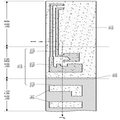
도 3a 내지 도 17b는 도 1a 및 도 1b에 도시된 반도체 소자를 형성하기 위한 반도체 소자의 제조 방법을 도시한 것으로서, 각각의 도면 중 a도는 반도체 소자의 단면도이고, b도는 반도체 소자의 평면도를 도시한다. 특히, a도는 b도의 I-I'에 따른 단면도에 해당한다. 또한, 도 4c는 셀 영역 및 연결 영역 상에 형성된 희생 패턴 구조물을 확대 도시한 평면도이다.3A to 17B illustrate a method of manufacturing a semiconductor device for forming the semiconductor device shown in FIGS. 1A and 1B, where a is a cross-sectional view of a semiconductor device, and b is a plan view of the semiconductor device. do. In particular, FIG. A corresponds to the cross-sectional view taken along line II ′ of FIG. 4C is an enlarged plan view of the sacrificial pattern structure formed on the cell region and the connection region.
도 3a 및 도 3b를 참조하면, 셀 영역, 연결 영역, 및 주변 영역을 포함하는 기판(100) 상에 식각 대상막(102)을 형성한다. 상기 식각 대상막(102)은 후속 공정을 통해 패터닝될 수 있고, 패터닝된 식각 대상막(102)은 하지막을 식각하기 위한 마스크 패턴으로 이용될 수 있다. 예를 들면, 상기 식각 대상막(102)은 실리콘 산화물을 증착시켜 형성할 수 있다. 상기 실리콘 산화물의 예로는 BPSG(boro-phospho silicate glass), TOSZ(tonen silazene), HDP(high density plasma), 및 PE-TEOS(plasma enhanced tetra-ethyl-orthyo-silicate glass) 등을 들 수 있다.3A and 3B, an
상기 식각 대상막(102) 상에 희생막(103)을 형성한다. 상기 희생막(103)은 영역에 따라 미세한 선폭 및 넓은 선폭을 각각 갖는 식각 마스크를 형성하기 위한 버퍼막으로 제공된다. 상기 희생막(103)은 제1 물질막(103a) 및 제2 물질막(103b)을 순차적으로 증착시켜 형성한다. A sacrificial layer 103 is formed on the
구체적으로, 상기 식각 대상막(102) 상에 제1 물질막(103a)을 형성한다. 상기 제1 물질막(103a)은 에싱 및 스트립 공정을 통해 용이하게 제거될 수 있는 폴리머 물질로 형성된다. 일 예로, 상기 제1 물질막(103a)은 스핀 온 하드 마스크(SOH)막질 또는 탄소 스핀 온 하드 마스크(C-SOH) 막질로써 이루어질 수 있다. 상기 제1 물질막(103a) 중 일부는 실질적인 식각 마스크로 사용되므로, 상기 제1 물질막(103a)은 식각 마스크로 사용되기에 충분한 두께를 갖도록 형성된다. In detail, a
상기 제1 물질막(103a) 상에 제2 물질막(103b)을 형성한다. 상기 제2 물질막(103b)은 실리콘 산 질화물(SiOxNy) 또는 실리콘 질화물(SiNx)을 증착시켜 형성할 수 있다. 상기 제2 물질막(103b)은 식각 마스크로 사용되지 않고 식각 대상막을 식각하기 이전에 모두 제거된다. 그러므로, 상기 제2 물질막(103b)은 상기 제1 물질막(103a)에 비해 얇은 두께로 형성한다. A
도 4a 내지 도 4c를 참조하면, 상기 희생막(103) 중 셀 영역 및 연결 영역에 형성된 희생막을 사진 식각 공정을 통해 패터닝함으로써, 희생 패턴 구조물(104)을 형성한다. 후술하겠지만, 후속 공정들을 통해 하나의 희생 패턴 구조물(104) 양 측벽으로 2개의 패턴들이 형성된다. 그러므로, 상기 희생 패턴 구조물(104)은 형성하고자 하는 패턴 구조물의 패턴 개수의 1/2만큼 형성한다. 4A through 4C, a
선택적으로, 주변 영역에 형성된 희생막은 패터닝되지 않거나, 적어도 소정 길이 이상의 선폭을 가지도록 패터닝될 수 있는데, 이는 주변 영역에서 발생할 수 있는 피팅(pitting) 현상을 방지하기 위함이다. 피팅 현상이란 희생막 중 제2 물질막의 일부가 원하지 않게 식각됨으로써 제 1 물질막의 상부가 노출되고, 그에 따라 후속 애싱 및 스트립 공정 동안 식각되지 않아야 할 제1 물질막의 일부가 식각되는 현상을 말한다. 제1 물질막은 식각 대상막의 식각 마스크로서 사용되기 때문에, 상기 피팅 현상에 의해 제1 물질막의 형상이 잘못 형성되는 경우 원하는 패턴이 형성되지 않는 문제점을 가진다. Optionally, the sacrificial film formed in the peripheral area may not be patterned or may be patterned to have a line width of at least a predetermined length, in order to prevent a fitting phenomenon that may occur in the peripheral area. The fitting phenomenon refers to a phenomenon in which a portion of the second material layer of the sacrificial layer is undesirably etched to expose an upper portion of the first material layer, thereby etching a portion of the first material layer that should not be etched during subsequent ashing and stripping processes. Since the first material film is used as an etching mask of the etching target film, a desired pattern is not formed when the shape of the first material film is incorrectly formed by the fitting phenomenon.
상기 희생 패턴 구조물(104)의 형상에 따라 이후에 형성되는 식각 마스크의 형상이 달라지므로, 형성하고자 하는 패턴 구조물의 형상에 따라 각각 다른 형상을 갖는 상기 희생 패턴 구조물(104)을 형성하여야 한다. 도시된 것과 같이, 상기 희생 패턴 구조물(104)은 제1 물질막 패턴(105a, 105c, 105e) 및 제2 물질막 패턴(105b, 105d, 105f)이 적층된 형상을 갖고, 상기 희생 패턴 구조물(104)의 선폭에 따라 상기 제2 물질막 패턴(105b, 105d)의 두께가 서로 다르다. Since the shape of the etch mask to be formed later depends on the shape of the
희생 패턴 구조물의 형상(104)에 따라 이후에 형성되는 식각 마스크의 형상이 달라지므로, 형상하고자 하는 패턴 구조물의 형상에 따라 각각 다른 형상을 가지는 희생 패턴 구조물(104)이 형성되어야 한다. 예를 들어, 연결 영역의 희생 패턴 구조물은 콘택 플러그와의 전기적 연결을 위한 패드를 형성하기 위한 것이므로, 셀 영역의 희생 패턴 구조물보다 더 넓은 선폭을 가지도록 형성될 수 있다.Since the shape of the etch mask subsequently formed depends on the
구체적으로, 상기 제2 물질막(103b) 상에 제1 포토레지스트막(도시안됨)을 코팅하고 이를 노광 및 현상 공정을 통해 패터닝함으로써, 제1 포토레지스트 패턴을 형성한다. 이 경우 상술한 피팅 현상을 방지하기 위해, 상기 제1 포토레지스트막 중 주변 영역에 형성된 제1 포토레지스트막은 패터닝되지 않거나, 소정 선폭 이상을 가지도록 패터닝될 수 있다. 상기 제 1 포토레지스트 패턴은 셀 영역에 형성된 좁은 선폭을 가지는 부분과 연결 영역에 형성된 상대적으로 넓은 선폭을 가지는 부분을 포함할 수 있다.Specifically, a first photoresist pattern is formed by coating a first photoresist layer (not shown) on the
상기 제1 포토레지스트 패턴을 식각 마스크로 사용하여 상기 제2 물질막(103b)을 식각한다. 이후, 식각된 상기 제2 물질막을 식각 마스크로 사용하여 상기 제1 물질막(103a)을 식각함으로써, 상기 제1 물질막 패턴(105a, 105c) 및 제2 물질막 패턴(105b, 105d)이 적층된 희생 패턴 구조물(104)을 형성한다. The
상기 식각 공정들을 수행할 때, 좁은 선폭을 갖는 부위의 제2 물질막 패턴(105b)은 3차원 효과(즉, 폭이 좁은 패턴의 단위 면적당 식각량이 폭이 넓은 패턴의 단위 면적당 식각량보다 큼)에 의해 상대적으로 넓은 선폭을 갖는 제2 물질막 패턴(105d)보다 식각 데미지를 더 많이 받게 된다. When performing the etching processes, the second material film pattern 105b of the portion having the narrow line width has a three-dimensional effect (that is, the etching amount per unit area of the narrow pattern is larger than the etching amount per unit area of the wide pattern). As a result, the etching damage is greater than that of the second
더욱 구체적으로, 좁은 선폭을 가지는 셀 영역의 제 2 물질막 패턴(105b)의 소모량이, 넓은 선폭을 가지는 연결 영역의 제 2 물질막 패턴(105d)의 소모량보다 더 큰 식각 조건 하에서, 제 1 물질막(105a, 105c)이 식각될 수 있다. 따라서, 상기 식각 공정을 수행하고 나면, 도 4a에 도시된 것과 같이, 상기 좁은 선폭을 갖는 라인 부분에는 상대적으로 제2 물질막 패턴(105b)이 더 얇게 남아있게 되고, 상기 넓은 선폭을 갖는 부분에는 상대적으로 제2 물질막 패턴(105d)이 더 두껍게 남아있게 된다. More specifically, under an etching condition in which the consumption of the second material film pattern 105b of the cell region having a narrow line width is larger than the consumption of the second
도면의 경우, 주변 영역에 형성된 제1 포토레지스트막은 패터닝되지 않았으므로, 주변 영역에 형성된 제1 물질막(105e) 및 제2 물질막(105f)은 패터닝되지 않은 채 잔존할 수 있다. 이와 같이 패터닝되지 않은 제 2 물질막(105f)은 주변에서 발생할 수 있는 피팅 현상을 방지할 수 있다.In the drawing, since the first photoresist film formed in the peripheral area is not patterned, the
상기 희생 패턴 구조물의 형상에 따라, 최종적으로 형성되는 패턴 구조물의 형상이 달라진다. 이하에서는, 본 실시예에 따른 희생 패턴 구조물의 형상을 설명한다. According to the shape of the sacrificial pattern structure, the shape of the finally formed pattern structure is different. Hereinafter, the shape of the sacrificial pattern structure according to the present embodiment will be described.
상기 희생 패턴 구조물(104)은 제1 방향으로 연장되고 제1 선폭(d1)을 갖는 희생 라인(104a)을 포함한다. 상기 희생 라인의 일 단부에 근접하여 상기 제1 방향과 수직하게 연결되고 상기 제1 선폭보다 넓은 선폭을 갖는 제1 희생 패드부(104b)를 포함한다. 또한, 상기 희생 라인의 일 단부와 연결되고 상기 제1 희생 패드부와 이격되면서 상기 제1 선폭보다 넓은 선폭을 갖는 제2 희생 패드부(104c)를 포함한다. The
후속 공정에서, 상기 희생 라인(104a)의 양 측벽에는 2개의 라인 형상의 식각 마스크들이 형성된다. 또한, 상기 희생 라인(104a)은 최종적으로 제거됨으로써 상기 라인 형상의 식각 마스크들을 서로 이격시킨다. 상기 식각 마스크들 사이의 이격 거리를 감소시키기 위하여, 상기 희생 라인(104a)은 사진 공정의 한계 선폭만큼 좁은 선폭을 가질 수 있다. 예를 들면, 상기 희생 라인(104a)은 약 40nm 내지 약 60nm 정도의 선폭을 가질 수 있다. In a subsequent process, two line etch masks are formed on both sidewalls of the
후속 공정에서, 상기 제1 희생 패드부(104b)는 1개의 라인 형상(즉,상기 2개의 라인 형상의 식각 마스크들 중 어느 하나)의 식각 마스크 패턴과 연결되는 패드 형상의 식각 마스크 패턴으로 형성된다. 또한, 상기 제2 희생 패드부(104c)는 나머지 1개의 라인 형상의 식각 마스크 패턴과 연결되는 패드 형상의 식각 마스크 패턴으로 형성된다.In a subsequent process, the first
희생 패턴 구조물(104) 중 주변 영역에 형성된 부분(104d)의 경우, 패터닝되지 않아 제1 물질막(105e) 및 제2 물질막(105f)이 주변 영역 전체에 걸쳐 연장되는 형태로 잔존한다. 이는 상술한 피팅 현상을 방지하기 위함이며, 주변 영역에 형성된 부분(104d)은 별도의 패터닝 공정을 거치게 된다. 상기 별도의 패터닝 공정에 대해서는 도 10a 및 도 10b에서 더욱 자세히 설명하기로 한다.In the case of the
도 4c에 도시된 것과 같이, 상기 제1 희생 패드부(104b)는 상기 희생 라인(104a)의 단부로부터 수직하게 연결되는 제1 예비 연장부(A)와 상기 제1 예비 연장부(A)와 연결되며 실질적으로 패드가 형성되는 부위인 제1 예비 패드부(B)를 포함한다. 상기 제2 희생 패드부(104c)는 상기 희생 라인(104a)과 동일한 방향으로 상기 희생 라인(104a)의 단부와 연결되는 제2 예비 연장부(A')와 상기 제2 예비 연장부와 실질적으로 패드가 형성되는 부위인 제2 예비 패드부(B')를 포함한다. 상기 제1 및 제2 예비 패드부들(B, B')은 형성하고자 하는 패드 크기와 유사한 크기로 형성되어야 한다. 또한, 상기 제1 및 제2 예비 연장부들(A, A') 중 적어도 하나는 상기 제1 방향과 수직하게 또는 상기 제1 방향과 일정 각도를 가지면서 꺾어진 형상을 갖는다. As shown in FIG. 4C, the first
한편, 상기 희생 패턴 구조물(104)의 희생 라인(104a)에서 상기 희생 패드부들(104b, 104c)의 반대편 단부들은 상기 제1 방향과 수직한 방향으로 꺾어진 형상을 갖는다. 이와는 다른 예로, 도시하지는 않았지만, 상기 희생 라인(104a)의 단부는 상기 제1 방향과 일정 각을 갖도록 꺾어진 형상을 가질 수도 있다. Meanwhile, opposite ends of the
상기 희생 패턴 구조물(104)에서 상기 꺾어진 부위의 선폭은 후속 공정에서 상기 희생 라인(104a)의 양 측벽에 형성되는 2개의 식각 마스크들이 서로 이격되는 거리가 된다. 상기 2개의 식각 마스크들의 단부가 서로 브릿지되지 않으면서 충분하게 이격되는 것이 바람직하다. 그러므로, 상기 희생 라인(104a)에서 상기 꺾어진 부위의 선폭은 상기 제1 선폭(d1)보다 넓은 것이 바람직하다. The line width of the bent portion of the
도 5a 및 도 5b를 참조하면, 상기 희생 패턴 구조물(104)의 표면 및 식각 대상막(102)의 상부면을 따라 스페이서 형성막(108)을 형성한다. 상기 스페이서 형성막(108)은 실리콘 산화물을 증착시켜 형성할 수 있다. 상기 스페이서 형성막(108)이 증착되는 두께는 이 후의 식각 마스크의 선폭과 동일하다. 그러므로, 상기 스페이서 형성막(108)은 형성하고자 하는 식각 마스크의 선폭과 동일한 두께로 형성한다. 상기 스페이서 형성막(108)은 사진 공정에 의해 형성할 수 있는 한계 선폭보다 더 작은 두께를 가질 수 있다. 이를 위해, 상기 스페이서 형성막(108)은 원자층 증착(atomic layer deposition) 공정을 이용하여 증착될 수 있다.5A and 5B, a
도 6a 및 도 6b를 참조하면, 상기 스페이서 형성막(108)을 덮도록 제2 포토레지스트막(미도시)을 코팅한다. 다음에, 사진 공정을 수행하여 제2 포토레지스트 패턴(110)을 형성한다. 6A and 6B, a second photoresist film (not shown) is coated to cover the
상기 제2 포토레지스트 패턴(110)은 상기 제1 및 제2 희생 패드부(104b, 104c) 사이에 위치하는 부위를 선택적으로 노출시키는 제1 개구부(112)를 포함한다. 구체적으로, 상기 제1 및 제2 희생 패드부(104b, 104c) 사이에서 상기 제1 방향과 수직한 방향으로 꺾어진 부위가 노출되어야 한다. 상기 제2 포토레지스트 패턴(110)의 제1 개구부(112)를 통해 상기 희생 패턴 구조물(104) 및 스페이서 형성막(108)의 일부분이 노출된다. 비록 도 6b에 도시되지는 않았지만, 도 6a에 나타난 바와 같이, 제1 개구부(112)는 희생 패턴 구조물(104)의 단부에서도 형성될 수 있다.The
상기 제2 포토레지스트 패턴(110)의 제1 개구부(112) 측벽으로부터 상기 희생 패턴 구조물(104)의 희생 라인(도 4c의 104a)의 외측벽까지의 거리(d2)가 적어도 약 30nm 내지 약 100nm 정도가 되도록 하는 것이 바람직하다. 상기 제1 개구부(112) 측벽이 상기 희생 패턴 구조물(104)의 외측벽과 지나치게 가까워지면 미스 얼라인에 의하여 불량이 발생될 수 있으며, 상기 제1 개구부(112) 측벽이 상기 희생 패턴 구조물(104)의 외측벽과 지나치게 멀어지면 완성되는 미세 패턴들이 서로 브릿지되어 쇼트 불량이 발생될 수 있다. The distance d2 from the sidewall of the
또한, 상기 제2 포토레지스트 패턴(110)은 상기 제1 및 제2 희생 패드부(104b, 104c) 반대편의 희생 라인(104a) 단부 외벽에 위치하는 스페이서 형성막(108)을 노출시킨다. In addition, the
도 7a 및 도 7b를 참조하면, 셀 영역 및 연결 영역의 제 1 개구부(도 6b의 112)에 위치하는 희생 패턴 구조물(104)의 일부 영역 및 상기 일부 영역 상의 스페이서 형성막(108)이 제거된다. 이를 위해, 상기 제2 포토레지스트 패턴(110)을 식각 마스크로 사용하여 노출되어 있는 상기 스페이서 형성막(108) 및 희생 패턴 구조물(104)을 식각한다. 7A and 7B, a portion of the
상기 식각 공정을 수행하면, 상기 제1 및 제2 희생 패드부(104b, 104c) 반대편의 희생 라인(104a) 단부에 위치하는 스페이서 형성막(108)이 식각되어 상기 스페이서 형성막(108)의 일 단부가 2개로 분리된다. When the etching process is performed, a
또한, 상기 식각 공정을 수행하면, 상기 희생 패턴 구조물(104)에서 상기 제1 및 제2 희생 패드부(104b, 104c) 사이에 제2 개구부(114)가 형성된다. 이 때, 상기 제2 개구부(114)의 측벽에는 상기 희생 패턴 구조물(104)의 측벽이 노출된다. 반면에, 상기 제2 개구부(114) 측벽 부위 및 상기 희생 라인(104a) 단부 이외에는 상기 희생 패턴 구조물(104)이 상기 스페이서 형성막(108)에 의해 모두 덮여있기 때문에 상기 희생 패턴 구조물(104)이 외부에 노출되지 않는다. In addition, when the etching process is performed, a
도 8a 및 도 8b를 참조하면, 상기 제2 포토레지스트 패턴(110)을 제거한다. 예를 들면, 상기 제2 포토레지스트 패턴(110)은 애싱 및/또는 스트립 공정을 통해 제거할 수 있다. 8A and 8B, the
상기 제2 포토레지스트 패턴(110)을 제거하는 공정에서, 상기 제2 개구부(114) 측벽 및 희생 라인(104a) 단부에서 노출되는 상기 희생 패턴 구조물(104)의 제1 물질막 패턴(105a)이 함께 제거될 수 있다. 상기 제1 물질막 패턴(105a)은 상기 제2 포토레지스트 패턴(110)과 식각 특성이 유사한 유기 폴리머 물질로 이루어지며, 상기 제2 포토레지스트 패턴(110)이 등방성으로 제거되므로, 상기 제2 포토레지스트 패턴(110)이 제거되면서 상기 제1 물질막 패턴(105a)의 일부도 함께 제거될 수 있다. 따라서, 상기 제2 포토레지스트 패턴(110) 및 제1 물질막 패턴(105a)이 제거되면서 상기 제2 개구부(114)의 하부 측방으로 홈(130)이 생성되고, 이로 인해 상기 제2 개구부(114)의 하부의 폭이 상부 폭에 비해 더 커지게 된다. 반면에, 상기 제2 포토레지스트 패턴(110)을 제거하는 공정에서, 식각선택비를 가지는 스페이서 형성막(108)에 둘러싸인 제 1 물질막 패턴(105a, 105c, 105e)의 경우 제거되지 않은 채 잔존한다.In the process of removing the
상기 제2 포토레지스트 패턴(110)을 제거하는 공정에서, 상기 제1 및 제2 희생 패드부(104b, 104c)의 하부가 서로 분리되도록 하여야 한다. 그러므로, 상기 제1 및 제2 희생 패드부(104b, 104c) 사이에 형성되어 있는 제1 물질막 패턴(105a)을 제거하여 상기 제2 개구부(114) 하부 측벽에 상기 희생 라인(104a) 양 측에 배치된 스페이서 형성막(108)이 각각 노출되도록 하여야 한다. 상기 제거 공정에서, 제1 및 제2 희생 패드부(104b, 104c)의 각 예비 연장부(A, A')의 하부가 제거되며, 실질적으로 패드가 형성되는 부위인 각각의 예비 패드부(B, B')는 제거되지 않도록 한다. In the process of removing the
한편, 상기 제2 포토레지스트 패턴(110)을 제거하는 공정에서, 상기 제2 물질막 패턴(105c)은 제거되지 않기 때문에, 상기 제1 및 제2 희생 패드부(104b, 104c) 상부는 서로 분리되지 않고 연결된 형상을 갖게 된다. In the process of removing the
도 9a 및 도 9b를 참조하면, 상기 스페이서 형성막(108)을 이방성으로 식각함으로써, 상기 희생 패턴 구조물(104)의 양 측벽에 각각 제1 내지 제3 스페이서(108a, 108b, 108c)를 형성한다. 9A and 9B, the
도시된 것과 같이, 상기 제2 개구부(114) 부위에는 상기 스페이서 형성막(108)이 이미 제거되었기 때문에 제1 및 제2 스페이서(108a, 108b)가 구비되지 않는다. 따라서, 하나의 희생 패턴 구조물(104)의 측벽에는 양쪽 단부가 각각 분리되어 있는 2개의 스페이서(108a, 108b)들이 형성된다. 또한, 분리된 하나의 스페이서(108a)는 상기 제1 희생 패드부(104b)의 측벽 부위를 감싸고, 분리된 나머지 스페이서(108b)는 상기 제2 희생 패드부(104c)의 측벽 부위를 감싸는 형상을 갖는다. As shown, the first and
한편, 셀 영역 및 주변 영역과 마찬가지로, 주변 영역의 패터닝되지 않은 희생 패턴 구조물(104) 상에 형성된 스페이서 형성막(108) 역시 이방성 식각됨으로써, 주변 영역의 희생 패턴 구조물(104)의 양 측벽에 제3 스페이서(108c)가 형성된다. 제3 스페이서(108c)는 제1 희생막(105e) 및 제2 희생막(105f)의 측벽을 감싸는 형상을 갖는다.Meanwhile, similarly to the cell region and the peripheral region, the
도 10a 및 도 10b를 참조하면, 상기 제1 및 제2 희생 패드부(104b, 104c)에 포함되어 있는 제2 물질막 패턴(105d)이 남아있도록 하면서, 상기 제1 선폭을 갖는 희생 라인(104a)에 포함되어 있는 상기 제2 물질막 패턴(105b)을 제거한다. 더욱 구체적으로, 좁은 선폭을 가지는 셀 영역의 제 2 물질막 패턴(105b)의 소모량이, 넓은 선폭을 가지는 연결 영역의 제 2 물질막 패턴(105d)의 소모량보다 더 큰 식각 조건 하에서, 제 2 물질막 패턴(105b, 105d)이 제거될 수 있다. 이러한 식각 조건은 상술한 3차원 효과에 기인한 것임은 상술한 바와 같다.10A and 10B, the
나아가, 도 4a 및 도 4b에 도시된 희생 패턴 구조물(104)의 형성 공정 결과, 상기 제1 선폭을 갖는 희생 라인(104a)에는 상대적으로 얇은 두께의 제2 물질막 패턴(105b)이 포함되고, 상기 제1 및 제2 희생 패드부(104b, 104c)에는 상대적으로 두꺼운 두께의 제2 물질막 패턴(105d)이 포함된다. 그러므로, 별도의 식각 마스크를 형성하지 않은 상태에서 식각 시간을 조절하여 상기 제2 물질막 패턴(105b, 105d)을 식각하면, 상기 희생 라인(104a)에 포함되어 있는 제2 물질막 패턴(105b)은 모두 제거되고, 나머지 희생 패드부(104b, 104c)에 포함되어 있는 제2 물질막 패턴(105d)은 남아있게 할 수 있다. Furthermore, as a result of the process of forming the
한편 주변 영역에 형성된 제2 물질막(105f)은 패터닝되지 않은 상태이므로, 제2 물질막 패턴(105b, 105d)의 식각 공정이 수행되더라도 상술한 3차원 효과에 의해 상대적으로 소량만이 제거된다. 따라서 제2 물질막(105f)은 여전히 제 1 물질막(105e)을 덮는 상태를 유지할 것이다.On the other hand, since the
상기 3차원 효과와 관련하여 상기 피팅 현상을 설명하면, 워드 라인과 같이 매우 좁은 선폭, 예를 들어 40 nm 이하의 선폭을 가지는 패턴은 3차원 효과에 의해 많은 식각 데미지를 받게 되고, 따라서 도 4a의 셀 영역에 도시된 바와 같이 상대적으로 얇은 제2 물질막 패턴(105b)만이 남아있게 된다. 한편 패드와 같이 두터운 선폭, 예를 들어 100nm 이상의 선폭을 가지는 패턴은 3차원 효과에 의해 적은 식각 데미지를 받게 되고, 따라서 도 4a의 연결 영역에 도시된 바와 같이 상대적으로 두꺼운 제 2 물질막 패턴(105d)이 남아있게 된다.Referring to the fitting phenomenon in relation to the three-dimensional effect, a pattern having a very narrow line width, for example, a line width of less than 40 nm, such as a word line is subjected to a lot of etching damage by the three-dimensional effect, and thus As shown in the cell region, only the relatively thin second material layer pattern 105b remains. On the other hand, a pattern having a thick line width such as a pad, for example, a line width of 100 nm or more is subjected to less etching damage by the three-dimensional effect, and thus, a relatively thick second
한편, 다양한 종류의 구동 회로를 구현하는 주변 영역의 경우, 형성되어야 할 패턴의 선폭의 종류가 다양하다. 예를 들어 주변 영역에 형성되어야 할 패턴의 선폭이 i) 셀 영역의 워드 라인과 같이 40nm 이하의 선폭을 요구할 수도 있고, ii) 연결 영역의 패드와 같이 100nm 이상의 선폭을 요구할 수도 있으며, iii) 40nm 내지 100nm 사이의 선폭을 요구할 수도 있다. 이 경우 i) 40nm 이하의 선폭과 iii) 100nm 이상의 선폭은 셀 영역 및 연결 영역과 동일한 방식의 공정을 적용함으로써 구현될 수 있다. 하지만 ii) 40nm 내지 100nm 사이의 선폭을 구현함에 있어서는, 도 4a에 나타난 3차원 효과에 의해 "강한 식각 데미지(40nm 이하의 선폭)"와 "약한 식각 데미지(100nm 이상의 선폭)" 사이의 "중간 정도의 식각 데미지"를 받게 된다. On the other hand, in the case of the peripheral area for implementing various kinds of driving circuits, there are various types of line widths of patterns to be formed. For example, the line width of the pattern to be formed in the peripheral area may require i) line width of 40 nm or less like the word line of the cell area, ii) line width of 100 nm or more like the pad of the connection area, and iii) 40 nm. Linewidths between 100 nm and 100 nm may be required. In this case, i) a line width of 40 nm or less and iii) a line width of 100 nm or more can be realized by applying the same process as the cell region and the connection region. However, ii) in realizing a line width between 40 nm and 100 nm, the "intermediate degree" between "strong etch damage (line width of 40 nm or less)" and "weak etch damage (line width of 100 nm or more)" by the three-dimensional effect shown in Fig. 4a. Etch damage ".
주변 영역에 형성된 제1 물질막(105e)과 제2 물질막(105f)이 패터닝된 경우, 제1 및 제2 물질막 패턴(미도시)은 40nm 내지 100nm 사이의 선폭으로 구현될 수 있다. 이 경우 상기 제1 물질막 패턴 상에 형성된 상기 제2 물질막 패턴이 온전히 남아있어야만 후속 공정에 의해 제1 물질막 패턴이 제거되지 않을 수 있다. 그러나, 40nm 내지 100nm의 선폭으로 구현된 상기 제2 물질막 패턴은 상기 "중간 정도의 식각 데미지"를 받게 되므로, 후속되는 더블 패터닝 공정(예를 들어, 도 10a의 식각 공정)에 의해 상기 제1 물질막 패턴의 상면 일부가 노출될 수 있다. 이 경우 제2 물질막의 일부가 원하지 않게 식각됨으로써 제 1 물질막의 상부가 노출되고, 그에 따라 식각되지 않아야 할 제1 물질막 일부가 식각되는 피팅 현상이 발생한다.When the
따라서 본 빌명의 기술 사상은 주변 영역에 형성된 패턴 구조물을 패터닝하지 않고(도 4a 참조), 추후 더블 패터닝 공정에 의한 미세 패턴의 형성 이후에 별도의 패터닝 공정(도 15a 참조)을 수행하는 것을 포함한다. 그에 따라 제1 물질막(도 4a의 105e) 및 제2 물질막(도 4a의 105f)은 주변 영역 전체에 걸쳐 연장되는 형태로 잔존하며, 이러한 제1 및 제 2 물질막(도 4a의 105e, 105f)은 매우 큰 선폭을 가지게 되므로 더블 패터닝 공정에 의한 피팅 현상이 발생하지 않게 된다.Accordingly, the technical idea of the present invention includes performing a separate patterning process (see FIG. 15A) after the formation of the fine pattern by the double patterning process without patterning the pattern structure formed in the peripheral region (see FIG. 4A). . Accordingly, the first material film (105e of FIG. 4A) and the second material film (105f of FIG. 4A) remain in a form extending over the entire peripheral area. The first and second material films (105e, FIG. 4A, Since 105f) has a very large line width, the fitting phenomenon by the double patterning process does not occur.
도 11a 및 도 11b를 참조하면, 노출된 상기 제1 물질막 패턴(105a)을 제거한다. 상기 제2 물질막 패턴(105d)이 남아있는 부위에는 상기 제1 물질막 패턴(105c)이 노출되어 있지 않으므로, 상기 제1 물질막 패턴(105c)이 제거되지 않고 남아있게 된다. 마찬가지로 주변 영역에 형성된 제2 물질막(105f)이 형성된 부위에는 제 1 물질막(105e)이 노출되어 있지 않으므로, 제 1 물질막(105e)이 제거되지 않고 남아있게 된다. 11A and 11B, the exposed first
상기 제1 물질막 패턴(105a)을 제거하는 공정은 이방성 식각 공정을 통해 수행될 수 있다. 그에 따라, 상기 제1 선폭을 갖는 희생 라인(104a) 사이에 위치하는 제1 물질막 패턴(105a)이 제거되면서 제1 및 제2 스페이서(108a, 108b) 사이에 갭이 생성된다. 반면에, 상기 제1 및 제2 희생 패드부(104b, 104c)에 포함되어 있는 제1 물질막 패턴(105c)은 그대로 남아있다. The process of removing the first
구체적으로, 도시된 것과 같이, 상기 제1 및 제2 희생 패드부(104b, 104c)에서 예비 연장부(A, A')에 해당하는 부위는 제2 물질막 패턴(105d)만이 남아 있어서 상기 제1 및 제2 희생 패드부(104b, 104c) 사이의 하부는 실질적으로 분리되어 있다. 또한, 상기 제1 및 제2 희생 패드부(104b, 104c)에서 예비 패드부(B, B')에 해당하는 부위는 제1 및 제2 물질막 패턴(105c, 105d)이 적층되어 있으며, 상기 예비 패드부(B. B') 측벽을 둘러싸는 제1 및 제2 스페이서(108a, 108b)도 남아있게 된다. Specifically, as shown in the drawing, only portions of the first and second
도 12a 및 도 12b를 참조하면, 남아있는 상기 제2 물질막 패턴(105d, 105f)을 모두 제거한다. 상기 제2 물질막 패턴(105d, 105f)을 모두 제거하면, 기판(100) 상의 식각 대상막(102)을 식각하기 위한 식각 마스크 패턴이 완성된다. 12A and 12B, all of the remaining second
셀 영역에서, 상기 식각 마스크 패턴은 제1 및 제2 스페이서(108a, 108b)를 포함한다. 셀 영역의 경우 제1 및 제 2 스페이서(108a, 108b) 사이에 형성된 제1 물질막 패턴(도 10a의 105a)이 제거되었으므로, 제1 및 제 2 스페이서(108a, 108b) 사이의 공간에 식각 대상막(102)의 상면이 노출된다.In the cell region, the etch mask pattern includes first and
연결 영역에서, 상기 식각 마스크 패턴은 제1 및 제2 스페이서(108a, 108b)와, 상기 제1 및 제2 스페이서(108a, 108b)의 일 단부와 각각 접하는 제1 및 제2 패드 마스크 패턴(118a, 118b)을 포함한다. 제1 및 제2 패드 마스크 패턴(118a, 118b)은 연결 영역에 잔존하는 제1 물질막(105c)과 대응된다.In the connection region, the etch mask patterns may include first and
마찬가지로, 주변 영역에서, 상기 식각 마스크 패턴은 제 3 스페이서(108c)와 제 3 스페이서(108c)의 단부와 접하는 벌크 마스크(118c)을 포함한다. 제1 및 제2 패드 마스크 패턴(118a, 118b)과 벌크 마스크(118c)는 제1 물질막(105c, 105e)으로 구성될 수 있다.Similarly, in the peripheral area, the etch mask pattern includes a
본 실시예의 상기 식각 마스크 패턴은 다음과 같은 형상을 갖는다. The etching mask pattern of this embodiment has a shape as follows.
셀 영역에서, 미세한 선폭을 갖는 제1 및 제2 스페이서(108a, 108b)가 라인 형상을 가지면서 서로 평행하게 배치된다. 상기 제1 및 제2 스페이서(108a, 108b)가 서로 이격되는 거리도 매우 좁다. In the cell region, the first and
연결 영역에서, 상기 식각 마스크 패턴은, 남아있는 제1 물질막 패턴(105c) 및 제1 물질막 패턴(105c)을 둘러싸는 제1 및 제2 스페이서(108a, 108b)를 포함할 수 있다. 따라서 상기 식각 마스크 패턴은 패드를 형성하기 위한 부위로 제공되는 제1 및 제2 패드 마스크 패턴(118a, 118b)을 포함한다. 도시된 것과 같이, 상기 제1 스페이서(108a)는 상기 제1 패드 마스크 패턴(118a)의 측벽을 둘러싸면서, 상기 제1 패드 마스크 패턴(118a)의 일 측방으로부터 돌출되는 돌출부(P)을 갖는다. 또한, 상기 제2 스페이서(108b)는 상기 제2 패드 마스크 패턴(118b)의 측벽을 둘러싸면서, 상기 제2 패드 마스크 패턴(118b)의 일 측방으로부터 돌출되는 돌출부(P)를 갖는다.In the connection region, the etch mask pattern may include the remaining first
연결 영역의 상기 스페이서(108a, 108b)의 돌출부(P)는, 상기 제2 포토레지스트 패턴(110)을 제거하는 공정에서 상기 제2 개구부 측벽(114)에 노출되어 있는 제1 및 제2 스페이서(108a, 108b)는 제거되지 않고 이웃하는 제1 물질막 패턴(105a)들이 일부 제거되면서 생성된 것이다. 즉, 상기 제1 물질막 패턴(105a)이 제거된 깊이만큼 상기 제1 및 제2 스페이서들(108a, 108b)이 측방으로 돌출된다. The protrusions P of the spacers 108a and 108b in the connection region may include first and second spacers exposed to the
주변 영역에서, 상기 식각 마스크 패턴은, 남아있는 제1 물질막(105e)으로 이루어지고, 구동 회로를 형성하기 위한 부분으로 제공되는 벌크 마스크(118c)를 포함한다. 상술한 바와 같이 피팅 현상을 방지하기 위해 벌크 마스크(118c)는 패터닝되지 않은 상태이며, 별도의 패터닝 공정을 통해 다양한 선폭을 자기는 패턴으로 형성될 것이다.In the peripheral area, the etch mask pattern includes a
도 13a 및 도 13b를 참조하면, 상기 식각 마스크 패턴을 이용하여 식각 대상막(102)을 식각함으로써 원하는 패턴 구조물(122)을 형성한다. 셀 영역 및 주변 영역에서 상기 패턴 구조물(122)은 서로 평행하게 배치되는 제1 및 제2 패턴(122a, 122b)을 포함하고, 주변 영역에서 상기 패턴 구조물(122)은 제3 패턴(122c)을 포함한다.13A and 13B, a desired
주변 영역의 제 3 패턴(122c)은 제3 스페이서(도 12의 108c) 및 벌크 마스크(도 12의 118c)에 의해 마스킹되어 형성된 것으로, 실질적으로 패터닝되지 않은 벌크 패턴에 해당한다. 이는 상술한 더블 패터닝 공정에 의해 발생할 수 있는 피팅 현상을 방지하기 위함이며, 별도의 공정을 통해 다양한 선폭을 가지는 패턴들로 형성될 것이다. The
도 8a 내지 도 13b를 참조로 설명한 공정들을 수행할 때, 사진 공정이 수반되지 않고 계속하여 막들의 식각만 이루어진다. 그러므로, 상기 도 8a 내지 도 13b를 참조로 설명한 공정들은 인-시튜(in-situ)로 진행할 수 있다.When performing the processes described with reference to FIGS. 8A-13B, only the etching of the films is continued without the photographic process involved. Therefore, the processes described with reference to FIGS. 8A through 13B may proceed in-situ.
이와 같이, 복잡한 사진 공정이 수반되지 않기 때문에 공정에 소요되는 비용이 감소되고, 인-시튜로 식각 공정들을 진행할 수 있으므로 공정 시간이 매우 단축되며 공정 불량이 감소될 수 있다.As such, since the complicated photographic process is not involved, the cost of the process is reduced, and since the etching processes can be performed in-situ, the process time can be very shortened and the process defect can be reduced.
도 14a 및 도 14b를 참조하면 식각 대상막인 패턴 구조물(122) 상에 제3 포토레지스트막(132)을 형성한다. 이후 제3 포토레지스트막(132)을 패터닝하기 위해, 제3 포토레지스트막(132)에 대한 사진 공정을 수행한다. 노광에 의해 제3 포토레지스트막(132)의 일부(132a)의 막질이 변화(예를들어, 알칼리 가용성으로 변화)될 수 있다.14A and 14B, a
상술한 바와 같이, 피팅 현상을 방지하기 위해 주변 영역의 회로 패턴(도 17b의 170)은 별도의 패터닝 공정을 통해 형성되며, 제3 포토레지스트막(132)은 상기 별도의 패터닝 공정을 수행하기 위해 형성된 것이다. 따라서 제3 포토레지스트막(132) 중 주변 영역 상에 형성된 포토레지스트막만이 사진 공정의 대상이 되고, 셀 영역 및 연결 영역 상에 형성된 포토레지스트막은 사진 공정의 대상이 되지 않을 수 있다.As described above, in order to prevent the fitting phenomenon, the
도 15a 및 도 15b를 참조하면, 제3 포토레지스트막(132)의 막질이 약해진 부분(도 14a의 132a)을 제거하여 제3 포토레지스트 패턴(140)을 형성한다. 제3 포토레지스트 패턴(140)에 의해 식각 대상막인 제3 패턴(122c)의 상면 일부를 노출시키는 제 3 개구부(135)가 형성된다.15A and 15B, the
상술한 바와 같이, 제3 포토레지스트 패턴(140)은 주변 영역 상에만 형성될 수 있고, 셀 영역 및 연결 영역 상의 포토레지스트막은 패터닝되지 않을 수 있다. 그러나 본 발명은 이에 제한되는 것은 아니며, 예를 들어 선택 트랜지스터(도 26의 SSL, GSL)의 게이트 라인을 형성하기 위해, 셀 영역 상의 포토레지스트막이 패터닝될수도 있다. 상기 실시예에 대해서는 도 27a 내지 도 29b에서 더욱 자세히 설명하기로 한다.As described above, the
도 16a 및 도 16b를 참조하면, 제3 포토레지스트 패턴(140)을 식각 마스크로 이용하여, 제 3 개구부(135)에 의해 노출된 제3 패턴(122c)을 식각한다. 벌크 패턴인 제3 패턴(122c)은 상기 식각 공정에 의해 복수개의 패턴(도 17a 및 도 17b의 170a, 170b)으로 분리된다.16A and 16B, the
이후 제3 포토레지스트 패턴(140)이 제거된 도 17a 및 도 17b를 참조하면, 셀 영역 및 연결 영역상에 제1 구조물(160)과 주변 영역 상에 제2 구조물(170)이 형성된다. 제1 구조물(160)은 제1 패턴(122a) 및 제2 패턴(122b)을 포함하고, 제2 구조물(170)은 복수개의 패턴(170a, 170b)을 포함할 수 있다.17A and 17B in which the
본 발명에 의하면, 단부에 상대적으로 넓은 폭을 갖는 패드를 포함하고 미세한 선폭을 갖는 패턴 구조물을 형성할 수 있다. 특히, 상기 라인 패턴과 패드를 각각의 패터닝 공정을 통해 형성하는 것이 아니기 때문에, 상기 라인 패턴과 패드가 서로 미스-얼라인되는 불량이 발생되지 않는다. According to the present invention, it is possible to form a pattern structure having a pad having a relatively wide width at the end and having a fine line width. In particular, since the line pattern and the pad are not formed through the respective patterning process, a defect in which the line pattern and the pad are miss-aligned with each other does not occur.
나아가, 본 발명의 기술 사상은 주변 영역 상에 형성되는 회로 패턴들이 피팅 현상에 의해 손상되는 것을 방지할 수 있다. 즉, 더블 패터닝 공정 동안 주변 영역에 형성된 식각 대상막을 패터닝하지 않고 별도의 사진 공정을 통해 주변 영역의 식각 대상막을 패터닝함으로써, 상술한 "중간 정도의 식각 데미지"를 받는 선폭을 가지는 패턴들이 피팅 데미지(pitting damage)를 받는 것을 방지할 수 있다.Furthermore, the technical idea of the present invention can prevent the circuit patterns formed on the peripheral area from being damaged by the fitting phenomenon. That is, by patterning the etch target layer of the peripheral region through a separate photographic process without patterning the etch target layer formed in the peripheral region during the double patterning process, the patterns having line widths subjected to the above-described “medium etch damage” are damaged by fitting ( It can prevent pitting damage.
도 18 내지 도 22b는 본 발명의 기술적 사상에 의한 실시예들에 따른 반도체 소자의 제조 방법을 공정 순서에 따라 도시한 단면도들이다. 이 실시예에 따른 반도체 소자의 제조 방법은 도 3a 내지 도 17b에 도시된 반도체 소자의 제조 방법을 일부 변형한 것이다. 이하 실시예들간의 중복되는 설명은 생략하기로 한다.18 to 22B are cross-sectional views illustrating a method of manufacturing a semiconductor device in accordance with exemplary embodiments of the inventive concept in a process sequence. The manufacturing method of the semiconductor device according to this embodiment is a modification of the manufacturing method of the semiconductor device shown in Figs. 3A to 17B. Duplicate descriptions between the embodiments will be omitted.
도 18을 참조하면, 기판은 반도체 기판(50), 소자 분리막(55), 터널링 절연층(60), 전하 저장층(70), 블로킹 절연층(80), 및 게이트 도전층(90)이 차례로 적층된 구조를 포함할 수 있다.Referring to FIG. 18, the
반도체 기판(50)은 예를 들어 실리콘, 실리콘-온-절연체(silicon-on-insulator), 실리콘-온-사파이어(silicon-on-sapphire), 게르마늄, 실리콘-게르마늄, 및 갈륨-비소(gallium-arsenide) 중 어느 하나를 포함할 수 있다. 반도체 기판(50)의 액티브 영역(A)은 소자 분리막(55)에 의해 정의될 수 있다.The
터널링 절연층(60)은 실리콘 산화물(SiO2), 실리콘 질화물(Si3N4), 실리콘 산질화물(SiON), 하프늄 산화물(HfO2), 하프늄 실리콘 산화물(HfSixOy), 알루미늄 산화물(Al2O3), 및 지르코늄 산화물(ZrO2) 중에 선택된 어느 하나 또는 이들의 조합으로 이루어진 복수의 층들이 적층된 것일 수 있다.The tunneling insulating
전하 저장층(70)은 비휘발성 메모리 소자의 데이터를 저장하는 기능을 수행하는 구성요소로서, 터널링 절연층(60) 상에 위치한다. 전하 트랩 플래시(charge trap flash) 방식에서, 전하 저장층(70)은 실리콘 질화층을 포함할 수 있다. 또한, 플로팅 게이트 방식에서, 전하 저장층(70)은 불순물이 도핑된 폴리실리콘을 포함할 수 있다. The
블로킹 절연층(80)은 전하 저장층(70) 상에 형성되어, 전하 저장층(70)에 저장된 전하가 게이트 도전층(90)으로 새는 것을 방지하는 기능을 수행한다. 블로킹 절연층(80)은, 하부 유전층, 고유전율 층, 및 상부 유전층이 차례로 적층된 구조를 포함할 수 있다. 주변 영역에 형성된 블로킹 절연층은 내부에 버팅 콘택 홀(butting contact hole, 85)을 포함할 수 있다.The blocking insulating
게이트 도전층(90)은 블로킹 절연층(80) 상에 형성될 수 있다. 게이트 도전층(80)은 불순물이 도핑된 폴리실리콘, 금속, 금속 실리사이드 물질 및 이들의 조합을 포함할 수 있다. 플로팅 게이트 타입의 플래시 메모리에서, 주변 영역에 형성된 게이트 도전층(90)은 버팅 콘택 홀(85) 내부를 채우도록 형성될 수 있고, 따라서 게이트 도전층(90)과 전하 저장층(70)이 전기적으로 연결될 수 있다.The gate
도 23 및 도 24를 참조하여 본 발명의 반도체 기판(50), 터널링 절연층(60), 전하 저장층(70), 소자 분리막(55), 및 블로킹 절연층(80)의 형성 과정을 더욱 자세히 설명하기로 한다.23 and 24, the process of forming the
도 23을 참조하면, 반도체 기판(50) 상에 터널링 절연층(60) 및 전하 저장층(70)을 차례로 형성하고, 전하 저장층(70), 터널링 절연층(60), 및 반도체 기판(50)을 패터닝하여 트렌치를 형성한다. 이후, 상기 트렌치 내부를 완전히 채우도록 절연층을 형성하고, 상기 절연층을 평탄화시킴으로써 소자 분리막(55)을 형성한다. 상기 평탄화는 화학 기계적 연마(chemical mechanical polishing, CMP) 공정, 에치 백(etch back) 공정 또는 화학 기계적 연마와 에치 백을 조합한 공정을 통해 수행될 수 있다.Referring to FIG. 23, a
여기서 셀 영역에 형성된 액티브 영역 및 소자 분리막(55a)은 매우 조밀하게(densely) 형성되는 반면, 주변 영역에 형성된 액티브 영역 및 소자 분리막(55b)은 성기게(sparsely) 형성될 수 있다. 따라서 셀 영역에 형성된 소자 분리막(55a)의 패턴 밀도는 주변 영역에 형성된 소자 분리막(55b)의 패턴 밀도보다 클 수 있다.The active region and the
이후, 도 24를 참조하면, 셀 영역 내 전하 저장층(70a)의 측면을 감싸도록 블로킹 절연층(미도시)을 형성하기 위해, 소자 분리막(55)을 식각하여 리세스가 형성되도록 한다. 상기 식각 공정은 전하 저장층(70)의 소모량보다 소자 분리막(55)의 소모량이 더 큰 식각 조건 하에서 수행될 수 있다. 이 경우 상술한 3차원 효과(즉, 폭이 좁은 패턴의 단위 면적당 식각량이 폭이 넓은 패턴의 단위 면적당 식각량보다 큼)에 의해, 주변 영역에 형성된 전하 저장층(70b) 보다 셀 영역에 형성된 전하 저장층(70a)이 더욱 많이 식각된다. 따라서 주변 영역에 형성된 전하 저장층(70b)과 셀 영역에 형성된 전하 저장층(70a)의 단차(즉, 높이 차이)가 발생할 수 있다.Subsequently, referring to FIG. 24, in order to form a blocking insulating layer (not shown) to surround the side of the
도 18의 전하 저장층(도 18의 70)은 도 24에서 설명된 단차가 나타나 있지는 않지만, 이는 공정 도시의 단순성을 위한 것이다. 따라서 셀 영역과 주변 영역에 형성된 전하 저장층(도 18의 70)의 높이는 서로 다를 수 있다.The charge storage layer of FIG. 18 (70 of FIG. 18) does not show the step described in FIG. 24, but this is for simplicity of process illustration. Therefore, the heights of the charge storage layers (70 in FIG. 18) formed in the cell region and the peripheral region may be different.
다시 도 18을 참조하면, 반도체 기판(50), 소자 분리막(55), 터널링 절연층(60), 전하 저장층(70), 블로킹 절연층(80), 및 게이트 도전층(90)을 포함하는 기판(100) 상에 형성된 식각 대상막에 대해 도 3a 내지 도 13b에 설명된 더블 패터닝 공정을 수행한다. 상기 더블 패터닝 공정에 의해 셀 영역에 제1 패턴(122a) 및 제2 패턴(122b)과 주변 영역에 제3 패턴(122c)을 형성한다.Referring back to FIG. 18, the
상술한 바와 같이, 더블 패터닝 공정에 의해 패터닝되지 않은 제3 패턴(122c)은 실질적으로 벌크 패턴에 해당한다. 피팅 현상을 방지하기 위해, 제3 패턴(122c)은 후술할 별도의 패터닝 공정을 통해 패터닝된다.As described above, the
도 19를 참조하면, 제1 패턴(122a), 제2 패턴(122b), 및 제3 패턴(122c)을 식각 마스크로 하여 게이트 도전층(90)에 대한 식각 공정을 수행한다. 상기 식각 공정에 의해 게이트 도전층(90) 사이의 공간에 블로킹 절연층(80)의 상면이 노출된다.Referring to FIG. 19, an etching process is performed on the gate
도 20을 참조하면, 블로킹 절연층(80), 게이트 도전층(90), 및 제1 내지 제3 패턴들(122a, 122b, 122c)을 덮도록 제3 포토레지스트막(132)을 형성하고, 상기 제3 포토레지스트막(132)을 패터닝하여 제3 포토레지스트 패턴(140)을 형성한다. Referring to FIG. 20, a
상술한 바와 같이, 더블 패터닝 공정 동안 "중간 정도의 식각 데미지"를 받는 선폭을 가지는 주변 영역의 회로 패턴들이 피팅 데미지를 받는 것을 방지하기 위해, 제3 포토레지스트 패턴(140)을 이용하여 별도의 패터닝 공정이 수행될 수 있다. 따라서, 제3 포토레지스트 패턴(140)을 형성하는 동안, 상기 제3 포토레지스트막 중 주변 영역 상의 포토레지스트막만이 패터닝되고, 셀 영역 및 연결 영역 상의 포토레지스트막(132)은 패터닝되지 않을 수 있다.As described above, in order to prevent the circuit patterns of the peripheral area having the line width subjected to “medium etch damage” during the double patterning process from receiving fitting damage, separate patterning is performed using the
도 21을 참조하면, 제3 포토레지스트 패턴(140)을 식각 마스크로 노출된 제3 패턴(122c) 및 게이트 도전층(90)을 식각한다. 상기 식각 공정에 의해, 제 3 패턴(122c)은 복수개의 패턴들(170a, 170b)로 분리될 수 있다. 또한, 선택적으로, 도 21에 나타난 바와 같이, 상기 식각 공정 동안 블로킹 절연층(80)이 더 식각될 수 있다.Referring to FIG. 21, the
이와 같이 셀 영역에 블로킹 절연층(80)이 남아 있음에도 주변 영역 상에 형성된 블로킹 절연층(80)을 먼저 식각하는 이유는, 도 23 및 도 24에서 설명한 바와 같이, 셀 영역과 주변 영역의 전하 저장층들(도 24의 70a, 70b) 사이에 단차가 존재하기 때문이다. 즉, 셀 영역과 주변 영역에 형성된 전하 저장층들(도 24의 70a, 70b)의 패턴 밀도 차이(도 24 참조)에 의해, 주변 영역에 형성된 전하 저장층(도 24의 70b)의 높이가 셀 영역에 형성된 전하 저장층(도 24의 70a)의 높이보다 클 수 있다. As described above with reference to FIGS. 23 and 24, the reason why the blocking insulating
이러한 높이 차이가 존재하는 상황에서 셀 영역과 주변 영역의 전하 저장층(70) 모두에 동일한 식각 공정을 진행할 경우, 셀 영역의 전하 저장층은 완전히 식각되지만, 주변 영역의 전하 저장층이 완전히 식각되지 않을 수 있다. 전하 저장층이 완전히 식각되지 않고 하부에 전하 저장층 일부가 잔존하는 경우, 식각된 전하 저장층 패턴들 사이에 스트링거(stringer) 불량과 같은 문제가 야기될 수 있다. In the case where such height difference exists, when the same etching process is performed on both the cell region and the
따라서, 도 21에 나타난 바와 같이, 상기 식각 공정 동안 제3 패턴(122c) 및 게이트 도전층(90) 뿐만 아니라, 블로킹 절연층(80)이 더 식각될 수 있다. 이 경우 추후 셀 영역과 주변 영역 모두에 동일한 식각 공정이 진행되더라도 셀 영역의 블로킹 절연층이 식각되는 동안 주변 영역의 전하 저장층이 식각될 수 있다. 따라서 셀 영역과 주변 영역간에 단차가 존재한다고 하더라도, 주변 영역의 전하 저장층이 잔존하지 않고 완전히 식각될 수 있다.Therefore, as shown in FIG. 21, the blocking insulating
도 22a 및 도 22b를 참조하면, 제3 포토레지스트막(132) 및 제3 포토레지스트 패턴(140)을 제거하고, 남아있는 제1 패턴(122a), 제2 패턴(122b), 및 제3 패턴(122c)을 포함하는 패턴 구조물(122)을 식각 마스크로, 액티브 영역(A) 상의 블로킹 절연층(80), 전하 저장층(70), 및 터널링 절연층(60)을 순차적으로 식각한다. 이 경우 소자 분리막(55) 상에서는, 블로킹 절연층(80) 및 소자 분리막(55) 일부가 식각될 수 있다. 또한, 상술한 바와 같이, 블로킹 절연층(80)은 셀 영역 상에서만 식각될 수 있고, 셀 영역의 블로킹 절연층(80)이 식각되는 동안 상대적으로 큰 높이를 가지는 주변 영역의 전하 저장층(70)이 식각됨으로써, 셀 영역과 주변 영역의 전하 저장층(70) 모두가 완전히 식각될 수 있다.Referring to FIGS. 22A and 22B, the
도 25는 NAND 플래시 메모리 소자의 셀의 회로도이다. 도 26은 도 1a 및 도 1b에 도시된 패턴 구조물을 포함하는 NAND 플래시 메모리 소자의 셀의 평면도이다 25 is a circuit diagram of a cell of a NAND flash memory device. FIG. 26 is a plan view of a cell of a NAND flash memory device including the pattern structure shown in FIGS. 1A and 1B.
도 25를 참조하면, 기판의 셀 영역에는 NAND 플래시 메모리 소자의 셀들이 구비된다. Referring to FIG. 25, cells of a NAND flash memory device are provided in a cell region of a substrate.
도시된 것과 같이, NAND 플래시 메모리 소자에서 상기 셀 영역에 형성되는 각각의 셀 스트링은 복수의 워드 라인들(WL1, WL2, WL3,..., WLm)을 포함한다. 일반적으로 하나의 스트링에는 32개 또는 64개의 워드 라인이 배치된다. 상기 워드 라인들(WL1, WL2, WL3,..., WLm)과 연결되어 단위 셀 트랜지스터들이 구비된다. 또한, 상기 복수의 워드 라인들(WL1, WL2, WL3,..., WLm)의 최외곽에는 각각 셀 선택 라인(SSL) 및 그라운드 선택 라인(GSL)이 배치된다. 상기 셀 선택 라인(SSL) 및 그라운드 선택 라인(GSL)과 연결되어 각각 셀 선택 트랜지스터 및 그라운드 선택 트랜지스터가 구비된다. As shown, each cell string formed in the cell region in a NAND flash memory device includes a plurality of word lines WL1, WL2, WL3,..., WLm. Generally, 32 or 64 word lines are arranged in one string. Unit cell transistors are connected to the word lines WL1, WL2, WL3,..., And WLm. In addition, a cell select line SSL and a ground select line GSL are disposed at the outermost sides of the plurality of word lines WL1, WL2, WL3,..., And WLm, respectively. A cell select transistor and a ground select transistor are connected to the cell select line SSL and the ground select line GSL, respectively.
상기 셀 선택 트랜지스터의 불순물 영역은 비트 라인(bit line)과 연결되고, 상기 그라운드 선택 트랜지스터의 불순물 영역은 공통 소오스 라인(GSL)과 연결된다. 상기 공통 소오스 라인(CSL)은 워드 라인들(WL1, WL2, WL3,..., WLm)의 방향으로 배치되어 있는 다른 스트링들을 서로 연결시키면서 연장된다. 또한, 도시된 것과 같이, 하나의 공통 소오스 라인(CSL)을 기준으로 셀 스트링들이 대칭적으로 배치되어 있다. An impurity region of the cell select transistor is connected to a bit line, and an impurity region of the ground select transistor is connected to a common source line GSL. The common source line CSL extends while connecting other strings arranged in the direction of the word lines WL1, WL2, WL3,..., WLm. In addition, as illustrated, the cell strings are arranged symmetrically with respect to one common source line CSL.
도 25에 도시된 NAND 플래시 셀 회로들은 기판 상에 구현된다. 상술한 바와 같이 기판은 반도체 기판, 터널링 절연층, 전하 저장층, 블로킹 절연층, 및 게이트 도전층이 차례로 적층된 구조를 포함할 수 있다.The NAND flash cell circuits shown in FIG. 25 are implemented on a substrate. As described above, the substrate may include a structure in which a semiconductor substrate, a tunneling insulating layer, a charge storage layer, a blocking insulating layer, and a gate conductive layer are sequentially stacked.
도 26을 참조하면, 반도체 기판의 상부면은 회로들이 구현되기 위한 액티브 영역 및 각 소자들을 전기적으로 분리시키기 위한 소자 분리 영역으로 구분된다. Referring to FIG. 26, an upper surface of a semiconductor substrate is divided into an active region for implementing circuits and an element isolation region for electrically separating the elements.
상기 액티브 영역은 제2 방향으로 연장되는 라인 형상을 갖고 반복적으로 배치되는 액티브 패턴(350)들을 포함한다. 상기 액티브 패턴(350)은 사진 공정의 한계 선폭만큼 좁은 선폭을 갖는다. 상기 액티브 패턴(350)들 사이에는 트렌치들(미도시)이 구비되며, 상기 트렌치들 내부에는 절연 물질이 채워짐으로써 소자 분리막 패턴들(미도시)이 구비된다. The active region includes
상기 액티브 패턴(350) 상에는 셀 트랜지스터(354), 워드 라인(360) 및 선택 트랜지스터(356)들이 구비된다. The
상기 셀 트랜지스터(354)는 터널링 절연층(도 29b의 60), 전하 저장층(도 29b의 70), 블로킹 절연층(도 29b의 80), 및 게이트 도전층(도 29b의 90)이 차례로 적층된 구조를 포함할 수 있다. 터널링 절연층(도 29b의 60)은 액티브 패턴(350)의 표면 상에 구비된다. 게이트 도전층(도 29b의 90)은 워드 라인(360)에 해당하고, 상기 워드 라인들(360) 각각은 제 1 방향으로 연장될 수 있다.The
상기 워드 라인(360)들은 상술한 본 발명의 기술적 사상에 의한 실시예들의 패턴 구조물 어레이의 형상을 가질 수 있다. 즉, 도 22b에 도시된 바와 같은 패턴 구조물(도 22b의 122)이 반복되는 패턴 구조물 어레이의 형상을 가질 수 있다. 각 워드 라인(360)들의 단부에는 상대적으로 넓은 선폭을 갖는 패드(361)가 연결되어 있다. 상기 패드(361)상에는 상기 패드(361)와 전기적으로 접촉하는 제1 콘택 플러그(368a)가 구비된다. The word lines 360 may have a shape of an array of pattern structures according to the embodiments of the inventive concept described above. That is, the pattern structure as shown in FIG. 22B (122 in FIG. 22B) may have a shape of a repeating pattern structure array.
상기 선택 트랜지스터(356)는 셀 트랜지스터(354)와 마찬가지로 터널링 절연층(도 29b의 60), 전하 저장층(도 29b의 70), 블로킹 절연층(도 29b의 80), 및 게이트 도전층(도 29b의 90)을 포함할 수 있다. 그러나 선택 트랜지스터는 데이터 저장의 기능을 필요로 하는 것이 아니므로, 터널링 절연층(도 29b의 60)은 게이트 절연층으로서 기능하고, 전하 저장층(도 29b의 70), 블로킹 절연층(도 29b의 80), 및 게이트 도전층(도 29b의 90)은 게이트 전극(362)으로서 기능한다. 전하 저장층(도 29b의 70) 및 게이트 도전층(도 29b의 90)이 하나의 게이트 전극(362)으로서 기능할 수 있도록, 블로킹 절연층(도 29b의 80)은 내부에 버팅 콘택 홀(85)을 포함할 수 있다.Like the
상기 게이트 전극(362)은 상기 제1 방향으로 연장되는 라인 형상을 갖는다. 상기 선택 트랜지스터(356)에 포함되는 게이트 전극(362)은 워드 라인(360)에 비해 충분히 넓은 선폭을 가질 수 있다.The
선택 트랜지스터(356)의 게이트 전극(362)와 마찬가지로, 주변 영역에 형성된 게이트 전극(390)에 포함된 터널링 절연층(도 29b의 60)은 게이트 절연층으로서 기능하고, 전하 저장층(도 29b의 70), 블로킹 절연층(도 29b의 80), 및 게이트 도전층(도 29b의 90)은 게이트 전극(362)으로서 기능할 수 있다. 또한 블로킹 절연층(도 29b의 80)은 내부에 버팅 콘택 홀(85)을 포함할 수 있다. 나아가, 주변 영역의 게이트 전극(390)은 워드 라인(360)에 비해 충분히 넓은 선폭을 가질 수 있다.Similar to the
상술한 바와 같이, 피팅 현상을 방지하기 위해 주변 영역에 형성된 게이트 전극(390)은 별도의 패터닝 공정을 통해 형성될 수 있다. 한편, 선택 트랜지스터의 게이트 전극(362) 역시 워드 라인(360)에 비해 넓은 선폭을 가질 수 있고, 따라서 피팅 현상이 발생할 수 있는 우려가 존재한다. 따라서 주변 영역의 게이트 전극(390)이 아닌 셀 영역의 게이트 전극(362) 대해서도 선택적으로 별도의 패터닝 공정이 적용될 수 있다. 이에 대해서는 도 27a 내지 도 29a에서 더욱 자세히 설명하기로 한다.As described above, the
도 27a 내지 도 29b는 본 발명의 기술적 사상에 의한 다른 실시예들에 따른 반도체 소자의 제조 방법을 공정 순서에 따라 도시한 단면도들이다. 각각의 도면 중 a도는 도 26의 A-A'를 따른 반도체 소자의 단면도이고, b도는 도 26의 B-B'를 따른 반도체 소자의 평면도를 도시한다. 이 실시예에 따른 반도체 소자의 제조 방법은 도 18 내지 도 22b에 도시된 반도체 소자의 제조 방법을 일부 변형한 것이다. 이하 실시예들간의 중복되는 설명은 생략하기로 한다.27A to 29B are cross-sectional views illustrating a method of manufacturing a semiconductor device in accordance with other embodiments of the inventive concept, in a process sequence. FIG. A is a cross sectional view of the semiconductor device along A-A 'of FIG. 26, and FIG. B is a plan view of the semiconductor device along B-B' of FIG. 26. The semiconductor device manufacturing method according to this embodiment is a modification of the manufacturing method of the semiconductor device shown in Figs. Duplicate descriptions between the embodiments will be omitted.
도 27a 를 참조하면, 셀 영역의 제1 및 제 2 패턴(122a, 122b)과 벌크 패턴(122d) 상에 제3 포토레지스트막(미도시)을 형성하고, 이후 상기 제3 포토레지스트막을 패터닝하여 벌크 패턴(122d)의 상면을 노출시키는 제3 포토레지스트 패턴(140)을 형성한다. 벌크 패턴(122d)은 선택 트랜지스터의 게이트 전극(도 26의 362)을 형성하기 위한 패턴으로서, 사진 공정의 한계 선폭보다 더 큰 선폭을 가질 수 있다.Referring to FIG. 27A, a third photoresist film (not shown) is formed on the first and
또한, 도 27b를 참조하면, 주변 영역의 제3 패턴(122c) 상에 상기 제3 포토레지스트막을 형성하고, 이후 상기 제3 포토레지스트막을 패터닝하여 주변 영역의 회로 패턴을 형성하기 위한 제3 포토레지스트 패턴(140)을 형성한다.In addition, referring to FIG. 27B, the third photoresist film is formed on the
도 28a를 참조하면, 셀 영역의 제3 포토레지스트 패턴(140)을 식각 마스크로 하여 노출된 벌크 패턴(122d), 게이트 도전층(90), 및 블로킹 절연층(80)을 차례로 식각한다. 벌크 패턴(122d)이 식각됨으로써 선택 트랜지스터 패턴(171)이 형성된다.Referring to FIG. 28A, the exposed
마찬가지로, 도 28b를 참조하면, 주변 영역의 제3 포토레지스트 패턴(140)을 식각 마스크로 하여 제 3 패턴(122c), 게이트 도전층(90), 및 블로킹 절연층(80)을 차례로 식각한다. 제 3 패턴(122c)이 식각됨으로써 주변 영역의 회로 패턴(170)이 형성된다.Similarly, referring to FIG. 28B, the
이후 도 29a를 참조하면, 셀 영역의 제3 포토레지스트 패턴(140)을 제거하고, 제1 및 제2 패턴(122a, 122b)과 벌크 패턴(122d)을 식각 마스크로 하여 블로킹 절연층(80), 전하 저장층(70), 및 터널링 절연층(60)을 차례로 식각한다. 상기 식각 공정에 의해 2개의 선택 트랜지스터(도 26의 356)가 형성될 수 있다.Thereafter, referring to FIG. 29A, the blocking insulating
또한, 도 29b를 참조하면, 셀 영역의 제3 포토레지스트 패턴(140)을 제거하고, 제1 및 제2 패턴(122a, 122b)과 벌크 패턴(122d)을 식각 마스크로 하여 블로킹 절연층(80), 전하 저장층(70), 터널링 절연층(60) 및 소자 분리막(55)을 차례로 식각한다. 상기 식각 공정에 의해 주변 영역의 게이트 전극(도 26의 390)이 형성될 수 있다.In addition, referring to FIG. 29B, the blocking insulating
이와 같이, 더블 패터닝 공정 이후 별도로 수행되는 사진 공정 동안, 주변 영역의 제3 패턴(122c) 뿐만 아니라, 셀 영역의 벌크 패턴(122d) 또한 패터닝될 수 있다. 따라서 더블 패터닝 공정을 적용할 경우 발생할 수 있는, 주변 영역의 제 3 패턴(122c)의 피팅 현상뿐만 아니라 셀 영역의 벌크 패턴(122d)의 피팅 현상도 또한 방지될 수 있다.As such, during the photographing process performed separately after the double patterning process, not only the
상술한 바와 같이 제 3 패턴(122c)은 주변 영역의 구동 회로를 형성하기 위한 마스크로서 이용되고, 벌크 패턴(122d)은 셀 영역의 선택 트랜지스터를 형성하기 위한 마스크로서 이용된다. As described above, the
도 30 내지 도 33b는 본 발명의 기술적 사상에 의한 실시예들에 따른 반도체 소자의 제조 방법을 공정 순서에 따라 도시한 것이다. 이 실시예에 따른 반도체 소자의 제조 방법 중 도 30 및 도 31은 도 23 및 도 24에 도시된 반도체 소자의 제조 방법을 일부 변형한 것이고, 도 32a 내지 도 33b는 도 28a 내지 도 29b에 도시된 반도체 소자의 제조 방법을 일부 변형한 것이다.30 to 33B illustrate a method of manufacturing a semiconductor device in accordance with embodiments of the inventive concept in the order of a process. 30 and 31 of the manufacturing method of the semiconductor device according to this embodiment are a modification of the manufacturing method of the semiconductor device shown in FIGS. 23 and 24, and FIGS. 32A to 33B are shown in FIGS. 28A to 29B. The manufacturing method of a semiconductor element is partially modified.
도 24에서 설명한 바와 같이, 소자 분리막(55)을 식각함으로써 주변 영역에 형성된 전하 저장층(70a)과 셀 영역에 형성된 전하 저장층(70b)의 단차가 발생할 수 있다. 이 경우, 도 30을 참조하면, 셀 영역에 형성된 전하 저장층(70a) 상에 포토레지스트 패턴(420)을 형성하고, 주변 영역의 전하 저장층만(70b)을 노출시킨다. 이후, 도 31을 참조하면, 주변 영역의 전하 저장층(70b)에 대한 식각 공정을 수행함으로써, 주변 영역에 형성된 전하 저장층(70b)과 셀 영역에 형성된 전하 저장층(70a)의 단차가 제거될 수 있다.As described with reference to FIG. 24, a step between the
즉, 상술한 반도체 소자의 제조 방법들(예를 들어, 도 18 내지 도 22b(및 도 23과 도 24)에 따른 반도체 소자의 제조 방법 또는 도 27a 내지 도 29b에 따른 반도체 소자의 제조 방법)은, 주변 영역에 형성된 전하 저장층과 셀 영역에 형성된 전하 저장층의 높이 차이 때문에 스트링거 불량이 발생할 우려가 있었다. 따라서 이를 방지하기 위해 별도의 사진 공정에 따른 식각 공정 동안 주변 영역에 형성된 블로킹 절연층을 미리 식각하였고, 그에 따라 셀 영역과 주변 영역 모두에 동일한 식각 공정이 진행되더라도 주변 영역의 전하 저장층이 완전히 식각될 수 있었다.That is, the above-described manufacturing method of the semiconductor device (for example, the manufacturing method of the semiconductor device according to FIGS. 18 to 22B (and FIGS. 23 and 24) or the manufacturing method of the semiconductor device according to FIGS. 27A to 29B) is However, stringer defects may occur due to the difference in height between the charge storage layer formed in the peripheral region and the charge storage layer formed in the cell region. Therefore, in order to prevent this, the blocking insulating layer formed in the peripheral region was previously etched during the etching process according to a separate photo process, and thus the charge storage layer in the peripheral region was completely etched even though the same etching process was performed in both the cell region and the peripheral region. Could be
그러나 이 실시예에 따른 반도체 소자의 제조 방법의 경우, 소자 분리막(55) 형성시 발생할 수 있는 전하 저장층(70a, 70b)의 높이 차이를 더블 패터닝 공정 전에 미리 제거하여 스트링거 불량의 문제를 방지하고 더블 패터닝 공정 및 사진 공정 등이 더욱 정밀하게 수행될 수 있다.However, in the method of manufacturing a semiconductor device according to this embodiment, the height difference of the
도 32a 및 도 32b를 참조하면, 스트링거 불량을 방지하기 위해 벌크 패턴(122d), 제3 패턴(122c), 게이트 도전층(90), 및 블로킹 절연층(80)을 차례로 식각하는 도 28a 및 도 28b와 달리, 셀 영역 및 주변 영역의 제3 포토레지스트 패턴(140)을 식각 마스크로 하여 노출된 벌크 패턴(122d), 제3 패턴(122c), 및 게이트 도전층(90)을 차례로 식각하고, 블로킹 절연층(80)은 식각하지 않는다.Referring to FIGS. 32A and 32B, FIGS. 28A and 32B sequentially etch the
도 33a 및 도 33b를 참조하면, 제3 포토레지스트 패턴(140)을 제거하고, 제1 및 제2 패턴(122a, 122b)과 벌크 패턴(122d)을 식각 마스크로 하여 블로킹 절연층(80), 전하 저장층(70a, 70b), 및 터널링 절연층(60)을 차례로 식각함으로써 선택 트랜지스터 및 회로 패턴을 형성한다. 도 24에 도시된 공정에 의해 셀 영역의 전하 저장층(70a)과 주변 영역의 전하 저장층(70b)의 높이가 동일해졌기 때문에, 주변 영역의 블로킹 절연층(80)이 따로 식각되지 않아도 된다.33A and 33B, the blocking insulating
도 34는 본 발명의 기술적 사상에 의한 실시예들에 따른 반도체 소자의 제조 방법에 의해 제조된 반도체 소자를 포함하는 카드(1000)를 보여주는 개략도이다.34 is a schematic diagram illustrating a
도 34를 참조하면, 컨트롤러(1010)와 메모리(1020)는 전기적인 신호를 교환하도록 배치될 수 있다. 예를 들어, 컨트롤러(1010)에서 명령을 내리면, 메모리(1020)는 데이터를 전송할 수 있다. 메모리(1020)는 본 발명의 실시예들 중 어느 하나에 따른 반도체 소자의 제조 방법에 의해 제조된 반도체 소자를 포함할 수 있다. 상기 반도체 소자들은 당해 기술 분야에서 잘 알려진 바와 같이 해당 로직 게이트 설계에 대응하여 "NAND" 및 "NOR" 아키텍쳐 메모리 어레이(미도시)로 배치될 수 있다. 복수의 행과 열로 배치된 메모리 어레이는 하나 이상의 메모리 어레이 뱅크(미도시)를 구성할 수 있다. 메모리(1020)은 이러한 메모리 어레이(미도시) 또는 메모리 어레이 뱅크(미도시)를 포함할 수 있다. 또한, 카드(1000)는 상술한 메모리 어레이 뱅크(미도시)를 구동하기 위하여 통상의 행디코더(미도시), 열디코더(미도시), I/O 버퍼들(미도시), 및/또는 제어 레지스터(미도시)를 더 포함할 수 있다. 이러한 카드(1000)는 다양한 종류의 카드, 예를 들어 메모리 스틱 카드(memory stick card), 스마트 미디어 카드(smart media card; SM), 씨큐어 디지털 카드(secure digital; SD), 미니 씨큐어 디지털 카드(mini secure digital card; mini SD), 또는 멀티 미디어 카드(multi media card; MMC)와 같은 메모리 장치에 이용될 수 있다.Referring to FIG. 34, the
도 35는 본 발명의 기술적 사상에 의한 실시예들에 따른 반도체 소자의 제조 방법에 의해 제조된 반도체 소자를 포함하는 시스템(1100)을 보여주는 개략도이다.35 is a schematic diagram illustrating a
도 35를 참조하면, 시스템(1100)은 컨트롤러(1110), 입/출력 장치(1120), 메모리(1130) 및 인터페이스(1140)을 포함할 수 있다. 시스템(1100)은 모바일 시스템 또는 정보를 전송하거나 전송받는 시스템일 수 있다. 상기 모바일 시스템은 PDA, 휴대용 컴퓨터(portable computer), 웹 타블렛(web tablet), 무선 폰(wireless phone), 모바일 폰(mobile phone), 디지털 뮤직 플레이어(digital music player) 또는 메모리 카드(memory card)일 수 있다. 컨트롤러(1110)는 프로그램을 실행하고, 시스템(1100)을 제어하는 역할을 할 수 있다. 컨트롤러(1110)는, 예를 들어 마이크로프로세서(microprocessor), 디지털 신호 처리기(digital signal processor), 마이크로콘트롤러(microcontroller) 또는 이와 유사한 장치일 수 있다. 입/출력 장치(1120)는 시스템(1100)의 데이터를 입력 또는 출력하는데 이용될 수 있다. 시스템(1100)은 입/출력 장치(1130)를 이용하여 외부 장치, 예컨대 개인용 컴퓨터 또는 네트워크에 연결되어, 외부 장치와 서로 데이터를 교환할 수 있다. 입/출력 장치(1120)는, 예를 들어 키패드(keypad), 키보드(keyboard) 또는 표시장치(display)일 수 있다. 메모리(1130)는 컨트롤러(1110)의 동작을 위한 코드 및/또는 데이터를 저장하거나, 및/또는 컨트롤러(1110)에서 처리된 데이터를 저장할 수 있다. 메모리(1130)는 본 발명의 실시예들 중 어느 하나에 따른 반도체 소자의 제조 방법에 의해 제조된 반도체 소자를 포함할 수 있다. 인터페이스(1140)는 상기 시스템(1100)과 외부의 다른 장치 사이의 데이터 전송통로일 수 있다. 컨트롤러(1110), 입/출력 장치(1120), 메모리(1130) 및 인터페이스(1140)는 버스(1150)를 통하여 서로 통신할 수 있다. 예를 들어, 이러한 시스템(1100)은 모바일 폰(mobile phone), MP3 플레이어, 네비게이션(navigation), 휴대용 멀티미디어 재생기(portable multimedia player, PMP), 고상 디스크(solid state disk; SSD) 또는 가전 제품(household appliances)에 이용될 수 있다.Referring to FIG. 35, the
본 발명을 명확하게 이해시키기 위해 첨부한 도면의 각 부위의 형상은 예시적인 것으로 이해하여야 한다. 도시된 형상 외의 다양한 형상으로 변형될 수 있음에 주의하여야 할 것이다. 도면들에 기재된 동일한 번호는 동일한 요소를 지칭한다.In order to clearly understand the present invention, the shape of each part of the accompanying drawings should be understood as illustrative. It should be noted that the present invention may be modified in various shapes other than the illustrated shape. Like numbers described in the figures refer to like elements.
이상에서 설명한 본 발명이 전술한 실시예 및 첨부된 도면에 한정되지 않으며, 본 발명의 기술적 사상을 벗어나지 않는 범위 내에서 여러 가지 치환, 변형 및 변경이 가능하다는 것은, 본 발명이 속하는 기술분야에서 통상의 지식을 가진 자에게 있어 명백할 것이다. It will be apparent to those skilled in the art that various modifications and variations can be made in the present invention without departing from the spirit or scope of the invention. Will be clear to those who have knowledge of.
Claims (10)
상기 식각 대상막 상에 희생막을 형성하는 단계;
상기 셀 영역 및 상기 연결 영역에 형성된 상기 희생막을 패터닝하여 희생 패턴 구조물을 형성하는 단계;
상기 희생 패턴 구조물의 측벽들을 덮는 스페이서를 형성하는 단계;
상기 셀 영역에서는 상기 스페이서를 식각 마스크로 이용하고, 상기 연결 영역에서는 상기 스페이서 및 상기 희생 패턴 구조물을 식각 마스크로 이용하여 상기 식각 대상막을 1차 식각하는 단계;
상기 식각 대상막 상에 포토레지스트막을 형성하고, 상기 주변 영역 상의 상기 포토레지스트막을 패터닝하여 상기 주변 영역 상에 포토레지스트 패턴을 형성하는 단계; 및
상기 포토레지스트 패턴을 식각 마스크로 이용하여 상기 식각 대상막을 2차 식각하는 단계를 포함하는 반도체 소자의 제조 방법.Forming an etching target layer on a substrate including a cell region, a connection region, and a peripheral region;
Forming a sacrificial layer on the etching target layer;
Patterning the sacrificial layer formed on the cell region and the connection region to form a sacrificial pattern structure;
Forming a spacer covering sidewalls of the sacrificial pattern structure;
First etching the etch target layer by using the spacer as an etch mask in the cell region and using the spacer and the sacrificial pattern structure as an etch mask in the connection region;
Forming a photoresist layer on the etching target layer and patterning the photoresist layer on the peripheral region to form a photoresist pattern on the peripheral region; And
And second etching the etch target layer using the photoresist pattern as an etch mask.
상기 포토레지스트 패턴을 형성하는 단계 동안, 상기 셀 영역 상의 상기 포토레지스트층이 더 패터닝되고,
상기 2차 식각하는 단계에 의해 식각된 상기 식각 대상막은, 상기 셀 영역에서는 선택 트랜지스터의 게이트 전극을 형성하기 위한 마스크로서 이용되고, 상기 주변 영역에서는 구동 회로의 게이트 전극을 형성하기 위한 마스크로서 이용되는 것을 특징으로 하는 반도체 소자의 제조 방법.The method of claim 1,
During the step of forming the photoresist pattern, the photoresist layer on the cell region is further patterned,
The etching target layer etched by the secondary etching is used as a mask for forming a gate electrode of a selection transistor in the cell region and as a mask for forming a gate electrode of a driving circuit in the peripheral region. The manufacturing method of the semiconductor element characterized by the above-mentioned.
상기 기판은 반도체 기판, 터널링 절연층, 전하 저장층, 블로킹 절연층, 및 게이트 도전층이 차례로 적층된 구조를 포함하고,
상기 1차 식각하는 단계 동안, 상기 셀 영역의 상기 게이트 도전층이 더 식각되는 것을 특징으로 하는 반도체 소자의 제조 방법.The method of claim 1,
The substrate includes a structure in which a semiconductor substrate, a tunneling insulating layer, a charge storage layer, a blocking insulating layer, and a gate conductive layer are sequentially stacked.
During the first etching, the gate conductive layer of the cell region is further etched.
상기 2차 식각하는 단계 동안, 상기 주변 영역의 상기 게이트 도전층이 더 식각되는 것을 특징으로 하는 반도체 소자의 제조 방법.The method of claim 3, wherein
During the secondary etching, the gate conductive layer of the peripheral region is further etched.
상기 희생막을 형성하는 단계는, 상기 기판 상에 제 1 물질막을 형성하는 단계 및 상기 제 1 물질막 상에 제 2 물질막 패턴을 형성하는 단계를 포함하고,
상기 희생 패턴 구조물을 형성하는 단계는, 상기 제 2 물질막 패턴을 식각 마스크로 이용하여 상기 제 1 물질막을 식각하여 제 1 물질막 패턴을 형성하는 단계를 포함하는 것을 특징으로 하는 반도체 소자의 제조 방법.The method of claim 1,
The forming of the sacrificial layer may include forming a first material layer on the substrate and forming a second material layer pattern on the first material layer.
The forming of the sacrificial pattern structure may include forming a first material layer pattern by etching the first material layer using the second material layer pattern as an etching mask. .
상기 제 1 물질막 패턴을 형성하는 단계 동안, 상기 제 2 물질막 패턴 중 상기 셀 영역에 형성된 제 2 물질막 패턴은 상기 주변 영역에 형성된 제 2 물질막 패턴보다 더 많이 식각되는 것을 특징으로 하는 반도체 소자의 제조 방법.The method of claim 5, wherein
During the forming of the first material layer pattern, the second material layer pattern formed in the cell region among the second material layer patterns is etched more than the second material layer pattern formed in the peripheral region. Method of manufacturing the device.
상기 스페이서를 형성하는 단계와 상기 1차 식각하는 단계 사이에,
상기 제 2 물질막 패턴 중 상기 셀 영역에 형성된 제 2 물질막 패턴의 식각 소모량이 상기 주변 영역에 형성된 제 2 물질막 패턴의 식각 소모량보다 더 큰 식각 조건 하에서, 상기 제 2 물질막 패턴을 제거하는 단계를 더 포함하는 것을 특징으로 하는 반도체 소자의 제조 방법.The method of claim 5, wherein
Between the forming of the spacer and the first etching step,
Removing the second material layer pattern under an etching condition in which the etching consumption of the second material layer pattern formed in the cell region among the second material layer patterns is greater than the etching consumption of the second material layer pattern formed in the peripheral region. The method of manufacturing a semiconductor device, further comprising the step.
상기 제 2 물질막 패턴을 제거하는 단계에 의해, 상기 제 1 물질막 패턴 중 상기 셀 영역에 형성된 제 1 물질막 패턴의 상면은 노출되고,
상기 연결 영역 및 상기 주변 영역에 형성된 제 1 물질막 패턴의 상면은 상기 제 2 물질막 패턴에 의해 덮이는 것을 특징으로 하는 반도체 소자의 제조 방법.The method of claim 7, wherein
By removing the second material film pattern, the upper surface of the first material film pattern formed in the cell region of the first material film pattern is exposed,
The upper surface of the first material film pattern formed in the connection region and the peripheral region is covered by the second material film pattern.
상기 식각 대상막 상에 희생막을 형성하는 단계;
상기 희생막을 패터닝하여 희생 패턴 구조물을 형성하는 단계;
상기 희생 패턴 구조물 상에 스페이서 형성막을 형성하는 단계;
상기 희생 패턴 구조물의 일부 영역 및 상기 일부 영역 상의 상기 스페이서 형성막을 제거하는 단계;
상기 스페이서 형성막을 식각하여, 상기 스페이서 형성막의 잔류 부분으로 이루어지는 상기 스페이서를 형성하는 단계;
상기 셀 영역에서는 상기 스페이서를 식각 마스크로 이용하고, 상기 연결 영역에서는 상기 스페이서 및 상기 희생 패턴 구조물을 식각 마스크로 이용하여 상기 식각 대상막을 1차 식각하는 단계;
상기 식각 대상막 상에 포토레지스트막을 형성하고, 상기 주변 영역 상의 상기 포토레지스트막을 패터닝하여 상기 주변 영역 상에 포토레지스트 패턴을 형성하는 단계; 및
상기 포토레지스트 패턴을 식각 마스크로 이용하여 상기 식각 대상막을 2차 식각하는 단계를 포함하는 반도체 소자의 제조 방법.Forming an etching target layer on a substrate including a cell region, a connection region, and a peripheral region;
Forming a sacrificial layer on the etching target layer;
Patterning the sacrificial layer to form a sacrificial pattern structure;
Forming a spacer forming layer on the sacrificial pattern structure;
Removing a portion of the sacrificial pattern structure and the spacer forming layer on the portion of the sacrificial pattern structure;
Etching the spacer forming film to form the spacer comprising a remaining portion of the spacer forming film;
First etching the etch target layer by using the spacer as an etch mask in the cell region and using the spacer and the sacrificial pattern structure as an etch mask in the connection region;
Forming a photoresist layer on the etching target layer and patterning the photoresist layer on the peripheral region to form a photoresist pattern on the peripheral region; And
And second etching the etch target layer using the photoresist pattern as an etch mask.
상기 희생 패턴 구조물의 측벽들을 덮는 스페이서를 형성하는 단계;
상기 셀 영역에서는 상기 스페이서를 식각 마스크로 이용하고, 상기 연결 영역에서는 상기 스페이서 및 상기 희생 패턴 구조물을 식각 마스크로 이용하여 상기 식각 대상막을 1차 식각하는 단계; 및
상기 주변 영역 상에 형성된 포토레지스트 패턴을 식각 마스크로 이용하여 상기 식각 대상막을 2차 식각하는 단계를 포함하는 반도체 소자의 제조 방법.Sequentially forming an etch target layer and a sacrificial pattern structure on a substrate including a cell region, a connection region, and a peripheral region;
Forming a spacer covering sidewalls of the sacrificial pattern structure;
First etching the etch target layer by using the spacer as an etch mask in the cell region and using the spacer and the sacrificial pattern structure as an etch mask in the connection region; And
And second etching the etch target layer using a photoresist pattern formed on the peripheral area as an etch mask.
Priority Applications (2)
| Application Number | Priority Date | Filing Date | Title |
|---|---|---|---|
| KR1020100103057A KR20120041558A (en) | 2010-10-21 | 2010-10-21 | Method of fabricating semiconductor device |
| US13/241,788 US8921233B2 (en) | 2010-10-21 | 2011-09-23 | Microelectronic fabrication methods using composite layers for double patterning |
Applications Claiming Priority (1)
| Application Number | Priority Date | Filing Date | Title |
|---|---|---|---|
| KR1020100103057A KR20120041558A (en) | 2010-10-21 | 2010-10-21 | Method of fabricating semiconductor device |
Publications (1)
| Publication Number | Publication Date |
|---|---|
| KR20120041558A true KR20120041558A (en) | 2012-05-02 |
Family
ID=45973386
Family Applications (1)
| Application Number | Title | Priority Date | Filing Date |
|---|---|---|---|
| KR1020100103057A Withdrawn KR20120041558A (en) | 2010-10-21 | 2010-10-21 | Method of fabricating semiconductor device |
Country Status (2)
| Country | Link |
|---|---|
| US (1) | US8921233B2 (en) |
| KR (1) | KR20120041558A (en) |
Cited By (1)
| Publication number | Priority date | Publication date | Assignee | Title |
|---|---|---|---|---|
| US9812501B2 (en) | 2015-01-05 | 2017-11-07 | Samsung Electronics Co., Ltd. | Variable resistance memory devices and methods of manufacturing the same |
Families Citing this family (9)
| Publication number | Priority date | Publication date | Assignee | Title |
|---|---|---|---|---|
| KR20150043759A (en) * | 2013-10-15 | 2015-04-23 | 에스케이하이닉스 주식회사 | Resistance variable memory apparatus and manufacturing method thereof |
| US9406522B2 (en) | 2014-07-24 | 2016-08-02 | Applied Materials, Inc. | Single platform, multiple cycle spacer deposition and etch |
| KR20160022637A (en) * | 2014-08-20 | 2016-03-02 | 삼성전자주식회사 | Method of fabricating flash memory device |
| US9324619B2 (en) * | 2014-08-25 | 2016-04-26 | Samsung Electronics Co., Ltd. | Semiconductor device and method of fabricating the same |
| KR102290460B1 (en) * | 2014-08-25 | 2021-08-19 | 삼성전자주식회사 | Semiconductor device and method of manufacturing the same |
| US20160365311A1 (en) * | 2015-06-10 | 2016-12-15 | Macronix International Co.Ltd. | Method of manufacturing semiconductor devices with combined array and periphery patterning in self-aligned double patterning |
| KR102480002B1 (en) | 2015-09-23 | 2022-12-22 | 삼성전자주식회사 | Semiconductor device and method of manufacturing the same and method of forming pattern |
| KR20170091833A (en) | 2016-02-01 | 2017-08-10 | 삼성전자주식회사 | Semiconductor device and method for manufacturing the same |
| US10418252B2 (en) | 2016-12-16 | 2019-09-17 | Taiwan Semiconductor Manufacturing Co, Ltd. | Fin-like field effect transistor patterning methods for increasing process margins |
Family Cites Families (4)
| Publication number | Priority date | Publication date | Assignee | Title |
|---|---|---|---|---|
| US7666578B2 (en) * | 2006-09-14 | 2010-02-23 | Micron Technology, Inc. | Efficient pitch multiplication process |
| JP2009049338A (en) | 2007-08-23 | 2009-03-05 | Toshiba Corp | Semiconductor device and manufacturing method thereof |
| KR101192359B1 (en) | 2007-12-17 | 2012-10-18 | 삼성전자주식회사 | NAND flash memory device and method for manufacturing the same |
| KR101540083B1 (en) | 2008-10-22 | 2015-07-30 | 삼성전자주식회사 | Method for pattern formation of semiconductor device |
-
2010
- 2010-10-21 KR KR1020100103057A patent/KR20120041558A/en not_active Withdrawn
-
2011
- 2011-09-23 US US13/241,788 patent/US8921233B2/en active Active
Cited By (1)
| Publication number | Priority date | Publication date | Assignee | Title |
|---|---|---|---|---|
| US9812501B2 (en) | 2015-01-05 | 2017-11-07 | Samsung Electronics Co., Ltd. | Variable resistance memory devices and methods of manufacturing the same |
Also Published As
| Publication number | Publication date |
|---|---|
| US8921233B2 (en) | 2014-12-30 |
| US20120100706A1 (en) | 2012-04-26 |
Similar Documents
| Publication | Publication Date | Title |
|---|---|---|
| US8921233B2 (en) | Microelectronic fabrication methods using composite layers for double patterning | |
| CN102024779B (en) | Pattern structures in semiconductor devices and method for forming the same | |
| US7811745B2 (en) | Method of manufacturing semiconductor device | |
| JP2009194244A (en) | Semiconductor memory device and manufacturing method thereof | |
| US20110032763A1 (en) | Semiconductor devices including first and second bit lines | |
| KR101360134B1 (en) | Method Of Fabricating Semiconductor Device | |
| KR100660543B1 (en) | NAND flash memory device and manufacturing method thereof | |
| US7541243B2 (en) | Methods of forming integrated circuit devices having gate electrodes formed on non-uniformly thick gate insulating layers | |
| US7320934B2 (en) | Method of forming a contact in a flash memory device | |
| US7560340B2 (en) | Method of manufacturing flash memory device | |
| US20250311210A1 (en) | Flash memory device and method for fabricating same | |
| KR20090127007A (en) | Non-volatile memory device having a shared bit line and manufacturing method thereof | |
| JP2010021496A (en) | Semiconductor device and method of manufacturing the same | |
| US20140043905A1 (en) | Semiconductor memory device and method of manufacturing the same | |
| JP2007073963A (en) | Split gate nonvolatile memory device and method of manufacturing the same | |
| US7381652B2 (en) | Method of manufacturing flash memory device | |
| KR100890400B1 (en) | A conductive structure, a method of forming the same, and a nonvolatile memory device comprising the same and a method of manufacturing the same. | |
| KR101263824B1 (en) | Nonvolatile memory device including double spacers on sidewall of floationg gate, electronic device including the nonvolatile memory device and method of fabricating the nonvolatile memory device | |
| CN103579362B (en) | Semiconductor device and manufacturing method thereof | |
| KR100649308B1 (en) | Flash memory device comprising a method of forming a self-aligned floating gate array and a self-aligned floating gate array | |
| KR19990018367A (en) | Nonvolatile Memory Device and Manufacturing Method Thereof | |
| US20090047764A1 (en) | Non-volatile memory and manufacturing method thereof | |
| TWI469253B (en) | Method of fabricating a flash and an isolating structure applied to a flash | |
| KR20100006944A (en) | Method of forming a isolation pattern and method of manufacturing a non-volatile memory device using the same | |
| CN112038344A (en) | Method for manufacturing floating gate memory element |
Legal Events
| Date | Code | Title | Description |
|---|---|---|---|
| PA0109 | Patent application |
St.27 status event code: A-0-1-A10-A12-nap-PA0109 |
|
| PG1501 | Laying open of application |
St.27 status event code: A-1-1-Q10-Q12-nap-PG1501 |
|
| R18-X000 | Changes to party contact information recorded |
St.27 status event code: A-3-3-R10-R18-oth-X000 |
|
| PC1203 | Withdrawal of no request for examination |
St.27 status event code: N-1-6-B10-B12-nap-PC1203 |
|
| WITN | Application deemed withdrawn, e.g. because no request for examination was filed or no examination fee was paid | ||
| P22-X000 | Classification modified |
St.27 status event code: A-2-2-P10-P22-nap-X000 |
|
| P22-X000 | Classification modified |
St.27 status event code: A-2-2-P10-P22-nap-X000 |
|
| P22-X000 | Classification modified |
St.27 status event code: A-2-2-P10-P22-nap-X000 |