KR20110111809A - Patterning method to realize stepped structure and manufacturing method of nonvolatile memory device using same - Google Patents
Patterning method to realize stepped structure and manufacturing method of nonvolatile memory device using same Download PDFInfo
- Publication number
- KR20110111809A KR20110111809A KR1020100031073A KR20100031073A KR20110111809A KR 20110111809 A KR20110111809 A KR 20110111809A KR 1020100031073 A KR1020100031073 A KR 1020100031073A KR 20100031073 A KR20100031073 A KR 20100031073A KR 20110111809 A KR20110111809 A KR 20110111809A
- Authority
- KR
- South Korea
- Prior art keywords
- mask
- etching
- forming
- film
- component
- Prior art date
- Legal status (The legal status is an assumption and is not a legal conclusion. Google has not performed a legal analysis and makes no representation as to the accuracy of the status listed.)
- Withdrawn
Links
Images


Classifications
-
- H—ELECTRICITY
- H10—SEMICONDUCTOR DEVICES; ELECTRIC SOLID-STATE DEVICES NOT OTHERWISE PROVIDED FOR
- H10B—ELECTRONIC MEMORY DEVICES
- H10B41/00—Electrically erasable-and-programmable ROM [EEPROM] devices comprising floating gates
- H10B41/20—Electrically erasable-and-programmable ROM [EEPROM] devices comprising floating gates characterised by three-dimensional arrangements, e.g. with cells on different height levels
- H10B41/23—Electrically erasable-and-programmable ROM [EEPROM] devices comprising floating gates characterised by three-dimensional arrangements, e.g. with cells on different height levels with source and drain on different levels, e.g. with sloping channels
- H10B41/27—Electrically erasable-and-programmable ROM [EEPROM] devices comprising floating gates characterised by three-dimensional arrangements, e.g. with cells on different height levels with source and drain on different levels, e.g. with sloping channels the channels comprising vertical portions, e.g. U-shaped channels
-
- H—ELECTRICITY
- H10—SEMICONDUCTOR DEVICES; ELECTRIC SOLID-STATE DEVICES NOT OTHERWISE PROVIDED FOR
- H10B—ELECTRONIC MEMORY DEVICES
- H10B41/00—Electrically erasable-and-programmable ROM [EEPROM] devices comprising floating gates
- H10B41/20—Electrically erasable-and-programmable ROM [EEPROM] devices comprising floating gates characterised by three-dimensional arrangements, e.g. with cells on different height levels
-
- H—ELECTRICITY
- H10—SEMICONDUCTOR DEVICES; ELECTRIC SOLID-STATE DEVICES NOT OTHERWISE PROVIDED FOR
- H10B—ELECTRONIC MEMORY DEVICES
- H10B41/00—Electrically erasable-and-programmable ROM [EEPROM] devices comprising floating gates
- H10B41/50—Electrically erasable-and-programmable ROM [EEPROM] devices comprising floating gates characterised by the boundary region between the core region and the peripheral circuit region
-
- H—ELECTRICITY
- H10—SEMICONDUCTOR DEVICES; ELECTRIC SOLID-STATE DEVICES NOT OTHERWISE PROVIDED FOR
- H10B—ELECTRONIC MEMORY DEVICES
- H10B43/00—EEPROM devices comprising charge-trapping gate insulators
- H10B43/20—EEPROM devices comprising charge-trapping gate insulators characterised by three-dimensional arrangements, e.g. with cells on different height levels
-
- H—ELECTRICITY
- H10—SEMICONDUCTOR DEVICES; ELECTRIC SOLID-STATE DEVICES NOT OTHERWISE PROVIDED FOR
- H10B—ELECTRONIC MEMORY DEVICES
- H10B43/00—EEPROM devices comprising charge-trapping gate insulators
- H10B43/50—EEPROM devices comprising charge-trapping gate insulators characterised by the boundary region between the core and peripheral circuit regions
-
- H10D64/01334—
-
- H—ELECTRICITY
- H10—SEMICONDUCTOR DEVICES; ELECTRIC SOLID-STATE DEVICES NOT OTHERWISE PROVIDED FOR
- H10D—INORGANIC ELECTRIC SEMICONDUCTOR DEVICES
- H10D88/00—Three-dimensional [3D] integrated devices
-
- H10P76/40—
-
- H10P76/4085—
Landscapes
- Semiconductor Memories (AREA)
- Non-Volatile Memory (AREA)
- Read Only Memory (AREA)
Abstract
본 발명은 계단형 구조를 구현할 수 있는 패터닝 방법 및 이를 이용한 불휘발성 메모리 소자의 제조 방법에 관한 것으로, 다수개의 박막을 플레이트 형태로 적층하고, 상기 다수개의 박막 중 최상층의 박막 상에 마스크를 형성하고, 상기 마스크를 이용한 에칭으로 상기 최상층의 박막을 패터닝하고, 상기 마스크를 순차 확대하고, 그리고 상기 순차 확대된 마스크를 이용한 에칭으로 나머지 박막들을 순차 패터닝하는 것을 포함하여, 상기 다수개의 박막을 상기 플레이트 형태에서 계단 형태로 형성하는 패터닝 방법을 이용하여 계단형 구조를 가진 컨트롤 게이트를 포함하는 불휘발성 메모리 소자를 제조할 수 있다.The present invention relates to a patterning method capable of implementing a stepped structure and a method of manufacturing a nonvolatile memory device using the same, wherein a plurality of thin films are stacked in a plate form, and a mask is formed on the thin film on the uppermost layer of the plurality of thin films. Patterning the plurality of thin films by the etching using the mask, sequentially enlarging the mask, and sequentially patterning the remaining thin films by etching using the sequentially enlarged mask. A nonvolatile memory device including a control gate having a stepped structure may be manufactured by using a patterning method of forming a stepped shape in.
Description
본 발명은 반도체 메모리 소자의 제조 방법에 관한 것으로, 보다 구체적으로는 계단형 구조를 구현할 수 있는 패터닝 방법 및 이를 이용한 불휘발성 메모리 소자의 제조 방법에 관한 것이다.The present invention relates to a method of manufacturing a semiconductor memory device, and more particularly, to a patterning method capable of implementing a stepped structure and a method of manufacturing a nonvolatile memory device using the same.
소비자가 요구하는 우수한 성능 및 저렴한 가격을 충족시키기 위해 반도체 소자의 집적도를 증가시키는 것이 요구되고 있다. 반도체 메모리 소자의 집적도는 제품의 가격을 결정하는 중요한 요인이기 때문에, 특히 증가된 집적도가 요구되고 있다. 종래의 2차원 또는 평면적 반도체 메모리 소자는 그 집적도가 단위 메모리 셀이 점유하는 면적에 의해 주로 결정되기 때문에, 미세 패턴 형성 기술의 수준에 크게 영향을 받는다. 하지만, 패턴의 미세화를 위해서는 초고가의 장비들이 필요하기 때문에, 2차원 반도체 메모리 장치의 집적도는 증가하고는 있지만 여전히 제한적이다. 이러한 한계를 극복하기 위하여 3차원적으로 배열되는 메모리 셀들을 구비하는 3차원 반도체 메모리 소자들이 제안되고 있다. 이러한 제안 중의 하나가 수직 낸드 플래시 메모리 소자이다.There is a demand for increasing the integration of semiconductor devices in order to meet the high performance and low price demanded by consumers. Since the degree of integration of semiconductor memory devices is an important factor in determining the price of a product, an increased degree of integration is particularly required. Conventional two-dimensional or planar semiconductor memory devices are greatly influenced by the level of fine pattern formation technology because their degree of integration is mainly determined by the area occupied by the unit memory cell. However, since expensive equipment is required for pattern miniaturization, the degree of integration of a two-dimensional semiconductor memory device is increasing but is still limited. To overcome this limitation, three-dimensional semiconductor memory devices having memory cells arranged three-dimensionally have been proposed. One such proposal is a vertical NAND flash memory device.
본 발명은 종래 기술에서의 필요성에 부응하기 위하여 안출된 것으로, 본 발명의 목적은 불휘발성 메모리 소자의 제조방법을 제공함에 있다.The present invention has been made to meet the needs of the prior art, and an object of the present invention is to provide a method of manufacturing a nonvolatile memory device.
본 발명의 다른 목적은 불휘발성 메모리 소자에 있어서 계단 형태의 게이트를 구현할 수 있는 패터닝 방법을 제공함에 있다.Another object of the present invention is to provide a patterning method capable of implementing a stepped gate in a nonvolatile memory device.
상기 목적을 구현할 수 있는 본 발명의 실시예에 따른 패터닝 방법은, 다수개의 박막을 플레이트 형태로 적층하고; 상기 다수개의 박막 중 최상층의 박막 상에 마스크를 형성하고; 상기 마스크를 이용한 에칭으로 상기 최상층의 박막을 패터닝하고; 상기 마스크를 순차 확대하고; 그리고 상기 순차 확대된 마스크를 이용한 에칭으로 나머지 박막들을 순차 패터닝하는 것을 포함하여, 상기 다수개의 박막을 상기 플레이트 형태에서 계단 형태로 형성하는 것을 포함할 수 있다.Patterning method according to an embodiment of the present invention that can achieve the above object, a plurality of thin films stacked in the form of a plate; Forming a mask on the thin film of the uppermost layer of the plurality of thin films; Patterning the thin film of the uppermost layer by etching using the mask; Sequentially enlarging the mask; And sequentially patterning the remaining thin films by etching using the sequentially enlarged mask, and forming the plurality of thin films in the form of a step in the form of a plate.
본 실시예의 패터닝 방법에 있어서, 상기 마스크를 순차 확대하는 것은 상기 마스크를 덮는 막을 증착하고; 그리고 상기 막을 스페이서 에칭하여 상기 마스크의 측벽에 스페이서를 형성하는 것을 포함할 수 있다.In the patterning method of this embodiment, the step of enlarging the mask sequentially deposits a film covering the mask; And forming a spacer on the sidewall of the mask by spacer etching the film.
본 실시예의 패터닝 방법에 있어서, 상기 막을 증착하는 것은 증착 성분과 에칭 성분이 포함된 가스를 제공하여 상기 마스크를 덮는 폴리머막을 증착하는 것을 포함할 수 있다.In the patterning method of the present embodiment, depositing the film may include depositing a polymer film covering the mask by providing a gas containing a deposition component and an etching component.
본 실시예의 패터닝 방법에 있어서, 상기 스페이서 에칭하는 것은 상기 가스를 제공하여 상기 폴리머 막의 일부를 제거하므로써 상기 마스크의 적어도 일측벽에 상기 스페이서를 형성하는 것을 포함할 수 있다.In the patterning method of the present embodiment, etching the spacer may include forming the spacer on at least one side wall of the mask by providing the gas to remove a portion of the polymer film.
본 실시예의 패터닝 방법에 있어서, 상기 막을 증착하는 것은 상기 증착 성분이 상기 에칭 성분에 비해 양이 많은 제1 가스를 제공하는 것을 포함할 수 있다.In the patterning method of this embodiment, depositing the film may include providing the first gas in which the deposition component is greater in amount than the etching component.
본 실시예의 패터닝 방법에 있어서, 상기 스페이서 에칭하는 것은 상기 에칭 성분이 상기 증착 성분에 비해 많은 제2 가스를 제공하여 상기 막을 증착하는 것과 인시튜로 진행하는 것을 포함할 수 있다.In the patterning method of the present embodiment, the spacer etching may include depositing the film by providing the second gas in which the etching component is larger than the deposition component and proceeding in situ.
본 실시예의 패터닝 방법에 있어서, 상기 증착 성분은 탄소(C) 혹은 탄소(C)/수소(H)를 포함하고, 상기 에칭 성분은 불소(F)를 포함할 수 있다.In the patterning method of the present embodiment, the deposition component may include carbon (C) or carbon (C) / hydrogen (H), and the etching component may include fluorine (F).
본 실시예에 있어서, 상기 제1 가스는 메틸플로라이드(CH3F)를 포함하고, 상기 제2 가스는 트리플루오로메탄(CHF3) 혹은 카본테트라플로라이드(CF4)를 포함할 수 있다.In the present embodiment, the first gas may include methyl fluoride (CH 3 F), and the second gas may include trifluoromethane (CHF 3 ) or carbon tetrafluoride (CF 4 ). .
본 실시예의 패터닝 방법에 있어서, 상기 제2 가스는 산소(O2)를 더 포함할 수 있다.In the patterning method of the present embodiment, the second gas may further include oxygen (O 2 ).
본 실시예의 패터닝 방법에 있어서, 상기 다수개의 박막을 플레이트 형태로 적층하는 것은 서로 다른 물질막들을 교대로 반복 적층하여 상기 다수개의 박막 각각을 상기 서로 다른 물질막들이 적층된 플레이트 형태로 형성하는 것을 포함할 수 있다.In the patterning method of the present embodiment, stacking the plurality of thin films in the form of a plate includes alternately repeatedly stacking different material layers to form each of the plurality of thin films in the form of a plate in which the different material layers are stacked. can do.
상기 목적을 구현할 수 있는 본 발명의 다른 실시예에 따른 패터닝 방법은, 다수개의 플레이트 형태를 가진 도전막들을 적층하고; 상기 도전막들 중 최상층 도전막 상에 마스크를 형성하고; 상기 마스크를 이용한 에칭으로 상기 최상층 도전막을 패터닝하고; 증착 성분과 에칭 성분이 혼합된 가스를 제공하되 상기 증착 성분을 상기 에칭 성분에 비해 더 많이 제공하여 상기 마스크를 덮는 폴리머막을 증착하고; 상기 가스를 제공하되 상기 에칭 성분을 상기 증착 성분에 비해 더 많이 제공하여 상기 폴리머막을 상기 마스크에 부착된 폴리머 스페이서로 형성하고; 상기 폴리머막의 증착과 스페이서 에칭을 순차 반복하여 상기 마스크를 순차 확대하고; 그리고 상기 순차 확대된 마스크를 이용한 에칭으로 나머지 도전막들을 순차 패터닝하여 상기 도전막들을 상기 플레이트 형태에서 계단형 형태로 형성하는 것을 포함할 수 있다.Patterning method according to another embodiment of the present invention that can achieve the above object is, laminating a plurality of conductive films having a plate shape; Forming a mask on an uppermost conductive film of the conductive films; Patterning the uppermost conductive film by etching using the mask; Providing a gas in which a deposition component and an etching component are mixed to provide more of the deposition component than the etching component to deposit a polymer film covering the mask; Providing the gas but providing more of the etching component than the deposition component to form the polymer film into a polymer spacer attached to the mask; Sequentially depositing the polymer film and spacer etching to sequentially enlarge the mask; And sequentially patterning the remaining conductive layers by etching using the sequentially enlarged mask to form the conductive layers in the step form from the plate form.
본 다른 실시예의 패터닝 방법에 있어서, 상기 폴리머 스페이서는 상기 마스크의 양측벽, 일측벽, 혹은 네측벽에 형성될 수 있다.In the patterning method of another embodiment, the polymer spacer may be formed on both side walls, one side wall, or four side walls of the mask.
본 다른 실시예의 패터닝 방법에 있어서, 상기 마스크를 형성하는 것은 상기 최상층 도전막의 상면 중에서 센터를 가로지르는 제1 포토레지스트 패턴; 상기 최상층 도전막의 상면 중에서 일측에 한정된 제2 포토레지스트 패턴; 및 상기 최상층 도전막의 상면 중에서 에지에 둘러싸인 센터에 한정된 제3 포토레지스트 패턴 중에서 어느 하나를 증착하는 것을 포함할 수 있다.In the patterning method of another embodiment, forming the mask comprises: a first photoresist pattern crossing a center of an upper surface of the uppermost conductive film; A second photoresist pattern defined on one side of an upper surface of the uppermost conductive film; And depositing any one of a third photoresist pattern defined at a center surrounded by an edge of an upper surface of the uppermost conductive layer.
본 다른 실시예의 패터닝 방법에 있어서, 상기 폴리머 스페이서는 상기 제1 포토레지스트 패턴의 양측벽에 형성되어, 상기 도전막들의 양측에 상기 계단형 형태가 구현될 수 있다.In the patterning method of another embodiment, the polymer spacer may be formed on both sidewalls of the first photoresist pattern, and the stepped shape may be implemented on both sides of the conductive layers.
본 다른 실시예의 패터닝 방법에 있어서, 상기 폴리머 스페이서는 상기 제2 포토레지스트 패턴의 일측벽에 형성되어, 상기 도전막들의 일측에 상기 계단형 형태가 구현될 수 있다.In the patterning method of another embodiment, the polymer spacer may be formed on one side wall of the second photoresist pattern, and the stepped shape may be implemented on one side of the conductive layers.
본 다른 실시예의 패터닝 방법에 있어서, 상기 폴리머 스페이서는 상기 제3 포토레지스트 패턴의 네측벽에 형성되어, 상기 도전막들의 네측벽에 상기 계단형 형태가 구현될 수 있다.In the patterning method of another embodiment, the polymer spacer may be formed on four sidewalls of the third photoresist pattern, and the stepped shape may be implemented on the four sidewalls of the conductive layers.
본 다른 실시예의 패터닝 방법에 있어서, 상기 폴리머막을 증착하는 것은 상기 증착 성분으로서 탄소(C)를 포함하고 상기 에칭 성분으로서 불소(F)를 포함하는 메틸플로라이드(CH3F)와, 아르곤(Ar) 및 질소(N2)가 포함된 플라즈마를 이용한 증착 공정을 이용할 수 있다.In the patterning method of another embodiment, depositing the polymer film comprises methyl fluoride (CH 3 F) containing carbon (C) as the deposition component and fluorine (F) as the etching component, and argon (Ar). ) And a deposition process using a plasma containing nitrogen (N 2 ) may be used.
본 다른 실시예의 패터닝 방법에 있어서, 상기 폴리머막을 폴리머 스페이서로 형성하는 것은 상기 증착 성분으로서 탄소(C)를 포함하고 상기 에칭 성분으로서 불소(F)를 포함하는 트리플루오로메탄(CHF3) 혹은 카본테트라플로라이드(CF4)와, 아르곤(Ar), 질소(N2) 및 산소(O2)가 포함된 플라즈마를 이용한 드라이 에칭 공정을 이용하되, 상기 증착 공정과 인시튜로 진행할 수 있다.In the patterning method of another embodiment, forming the polymer film with a polymer spacer comprises trifluoromethane (CHF 3 ) or carbon containing carbon (C) as the deposition component and fluorine (F) as the etching component. A dry etching process using a plasma containing tetrafluoride (CF 4 ), argon (Ar), nitrogen (N 2 ), and oxygen (O 2 ) may be used, but may proceed in situ with the deposition process.
본 다른 실시예의 패터닝 방법에 있어서, 상기 도전막들 사이에 플레이트 형태를 가진 절연막들을 형성하는 것을 더 포함할 수 있다. 상기 순차 확대된 마스크를 이용한 에칭으로 상기 절연막들을 상기 플레이트 형태에서 계단형 형태로 형성할 수 있다.In the patterning method of another exemplary embodiment, the method may further include forming insulating layers having a plate shape between the conductive layers. The insulating layers may be formed in a stepped shape in the form of a plate by etching using the sequentially enlarged mask.
상기 목적을 구현할 수 있는 본 발명의 실시예에 따른 불휘발성 메모리 소자의 제조방법은, 반도체 기판 상에 하부 선택 게이트를 형성하고; 상기 하부 선택 게이트 상에 계단형 구조를 이루는 다수개의 컨트롤 게이트를 형성하고; 상기 컨트롤 게이트 상에 상부 선택 게이트를 형성하고; 그리고 상기 게이트들을 관통하여 상기 반도체 기판과 연결되는 활성 기둥을 형성하는 것을 포함하되, 상기 컨트롤 게이트를 형성하는 것은: 상기 다수개의 컨트롤 게이트를 플레이트 형태로 적층하고; 상기 다수개의 컨트롤 게이트 중 최상층의 컨트롤 게이트 상에 마스크를 형성하고; 상기 마스크를 이용한 에칭으로 상기 최상층의 컨트롤 게이트를 패터닝하고; 상기 마스크를 순차 확대하고; 그리고 상기 순차 확대된 마스크를 이용한 에칭으로 나머지 컨트롤 게이트들을 패터닝하므로써 상기 플레이트 형태를 상기 계단형 구조로 형성하여, 상기 다수개의 컨트롤 게이트 각각에 워드라인 패드를 정의하는 것을 포함할 수 있다.According to another aspect of the present invention, there is provided a method of manufacturing a nonvolatile memory device, including: forming a lower selection gate on a semiconductor substrate; Forming a plurality of control gates having a stepped structure on the lower selection gate; Forming a top select gate on the control gate; And forming an active pillar penetrating through the gates and connected to the semiconductor substrate, wherein forming the control gate comprises: stacking the plurality of control gates in a plate form; Forming a mask on a control gate of a top layer of the plurality of control gates; Patterning the control gate of the uppermost layer by etching with the mask; Sequentially enlarging the mask; And forming the plate shape into the stepped structure by patterning the remaining control gates by etching using the sequentially enlarged mask, thereby defining a word line pad in each of the plurality of control gates.
본 실시예의 제조방법에 있어서, 상기 마스크를 순차 확대하는 것은 증착 성분과 에칭 성분이 포함된 가스를 제공하여 상기 마스크를 덮는 폴리머막을 증착하고; 그리고 상기 가스를 제공하여 상기 폴리머 막의 일부를 제거하므로써 상기 마스크의 적어도 일측벽에 폴리머 스페이서를 형성하는 것을 포함할 수 있다.In the manufacturing method of this embodiment, the step of enlarging the mask sequentially comprises: providing a gas containing a deposition component and an etching component to deposit a polymer film covering the mask; And providing a gas to remove a portion of the polymer film to form a polymer spacer on at least one side wall of the mask.
본 실시예의 제조방법에 있어서, 상기 폴리머 스페이서를 형성하는 것은 상기 폴리머막을 증착하는 것과 인시튜로 진행하되, 상기 폴리머막을 증착하는 것과 다르게 상기 증착 및 에칭 성분의 양을 다르게 설정할 수 있다.In the manufacturing method of the present embodiment, the formation of the polymer spacer may proceed in situ with the deposition of the polymer film, but the deposition and etching components may be set differently from the deposition of the polymer film.
본 실시예의 제조방법에 있어서, 상기 폴리머막을 증착하는 것은 상기 증착 성분을 상기 에칭 성분에 비해 더 많이 제공하고, 상기 폴리머 스페이서를 형성하는 것은 상기 에칭 성분을 상기 증착 성분에 비해 더 많이 제공할 수 있다.In the manufacturing method of the present embodiment, depositing the polymer film may provide the deposition component more than the etching component, and forming the polymer spacer may provide the etching component more than the deposition component. .
본 실시예의 제조방법에 있어서, 상기 증착 성분은 탄소(C)를 포함하고, 상기 에칭 성분은 불소(F)를 포함할 수 있다.In the manufacturing method of the present embodiment, the deposition component may include carbon (C), and the etching component may include fluorine (F).
본 실시예의 제조방법에 있어서, 상기 폴리머막을 증착하는 것은 메틸플로라이드(CH3F), 질소(N2) 및 아르곤(Ar)을 포함하는 플라즈마를 이용한 증착 공정을 이용할 수 있다.In the manufacturing method of the present embodiment, the deposition of the polymer film may use a deposition process using a plasma containing methyl fluoride (CH 3 F), nitrogen (N 2 ) and argon (Ar).
본 실시예의 제조방법에 있어서, 상기 폴리머 스페이서를 형성하는 것은 트리플루오로메탄(CHF3) 혹은 카본테트라플로라이드(CF4), 질소(N2), 및 아르곤(Ar)을 포함하는 플라즈마를 이용한 에칭 공정을 이용할 수 있다.In the manufacturing method of the present embodiment, the polymer spacer is formed by using a plasma containing trifluoromethane (CHF 3 ) or carbon tetrafluoride (CF 4 ), nitrogen (N 2 ), and argon (Ar). Etching processes can be used.
본 실시예의 제조방법에 있어서, 상기 폴리머 스페이서를 형성하는 것은 상기 플라즈마에 산소(O2)가 더 포함된 에칭 공정을 이용할 수 있다.In the manufacturing method of the present embodiment, forming the polymer spacer may use an etching process in which oxygen (O 2 ) is further included in the plasma.
상기 목적을 구현할 수 있는 본 발명의 다른 실시예에 따른 불휘발성 메모리 소자의 제조방법은, 반도체 기판 상에 절연막들과 희생막들을 플레이트 형태로 반복 적층하여 박막 구조체를 형성하고; 상기 박막 구조체 상에 마스크를 형성하되, 상기 마스크를 순차 확대하고; 상기 순차 확대되는 마스크를 이용한 에칭으로 상기 박막 구조체를 패터닝하여 상기 플레이트 형태를 계단형 형태로 형성하고; 상기 희생막들을 선택적으로 제거하여 상기 절연막들 사이에 리세스 영역들을 형성하고; 그리고 상기 리세스 영역들을 도전막들로 채워 계단형 구조로 적층된 게이트들을 형성하는 것을 포함할 수 있다.According to another aspect of the present invention, there is provided a method of manufacturing a nonvolatile memory device, the thin film structure being formed by repeatedly stacking insulating films and sacrificial films on a semiconductor substrate in the form of a plate; Forming a mask on the thin film structure, wherein the mask is sequentially enlarged; Patterning the thin film structure by etching using the sequentially enlarged mask to form the plate shape in a stepped shape; Selectively removing the sacrificial layers to form recess regions between the insulating layers; The method may include filling the recess regions with conductive layers to form gates stacked in a stepped structure.
본 다른 실시예의 제조방법에 있어서, 상기 마스크를 순차 확대하는 것은 증착 성분과 에칭 성분을 포함하는 가스를 제공하여 상기 마스크를 덮는 폴리머막을 증착하고, 그리고 인시튜로 상기 폴리머 막을 에칭하여 상기 마스크의 적어도 일측벽에 폴리머 스페이서를 형성하는 것을 포함할 수 있다. 상기 폴리머 막 증착시에는 상기 증착 성분을 상기 에칭 성분에 비해 더 많이 제공하고, 상기 폴리머 막 에칭시에는 상기 에칭 성분을 상기 증착 성분에 비해 더 많이 제공할 수 있다.In the manufacturing method of another embodiment, the step of enlarging the mask sequentially provides a gas comprising a deposition component and an etching component to deposit a polymer film covering the mask, and in situ etching the polymer film to at least It may include forming a polymer spacer on one side wall. The deposition of the polymer film may provide more of the deposition component than the etching component, and the etching of the polymer film may provide more of the etching component than the deposition component.
본 다른 실시예의 제조방법에 있어서, 상기 폴리머 막 증착시에는 메틸플로라이드(CH3F)를 포함하는 플라즈마를 이용하고, 상기 폴리머 막 에칭시에는 트리플루오로메탄(CHF3) 혹은 카본테트라플로라이드(CF4)를 포함하는 플라즈마를 이용할 수 있다.In another embodiment of the present invention, a plasma containing methyl fluoride (CH 3 F) is used to deposit the polymer film, and trifluoromethane (CHF 3 ) is used to etch the polymer film. Alternatively, plasma containing carbon tetrafluoride (CF 4 ) may be used.
본 다른 실시예의 제조방법에 있어서, 상기 리세스 영역들을 형성하는 것은 상기 박막 구조체를 일부 제거하여 상기 반도체 기판 혹은 상기 절연막들 중 최하층을 노출시키는 트렌치를 형성하고; 그리고 상기 트렌치를 통해 상기 박막 구조체에 에천트를 제공하여 상기 희생막들을 선택적으로 제거하는 것을 포함할 수 있다.In the manufacturing method of another embodiment, the forming of the recess regions may partially remove the thin film structure to form a trench that exposes a lowermost layer of the semiconductor substrate or the insulating films; And selectively removing the sacrificial layers by providing an etchant to the thin film structure through the trench.
본 발명에 의하면, 마스크 측벽에 스페이서를 부착하여 컨트롤 게이트를 계단형 구조로 패터닝할 수 있다. 특히 폴리머를 이용하여 스페이서를 형성하는 경우 인시튜 공정이 가능하여 공정 간소화 및 공정 불량을 최대한 억제할 수 있어 제조비용을 감소시킬 수 있는 효과가 있다.According to the present invention, the control gate may be patterned in a stepped structure by attaching a spacer to the mask sidewall. In particular, when the spacer is formed using a polymer, an in-situ process is possible, so that process simplification and process defects can be suppressed as much as possible, thereby reducing manufacturing costs.
도 1a는 본 발명의 실시예에 따른 불휘발성 메모리 소자를 도시한 사시도.
도 1b는 도 1a의 셀 영역을 도시한 사시도.
도 1c 및 도 1d는 도 1b의 메모리 트랜지스터를 도시한 사시도.
도 1e는 본 발명의 실시예에 따른 불휘발성 메모리 소자의 등가회로도.
도 2a 내지 2h는 본 발명의 실시예에 따른 불휘발성 메모리 소자의 제조방법을 도시한 사시도.
도 3a 내지 3l은 본 발명의 실시예에 따른 계단형 구조를 구현할 수 있는 패터닝 방법을 도시한 사시도.
도 4a는 본 발명의 다른 실시예에 따른 불휘발성 메모리 소자를 도시한 사시도.
도 4b 및 4c는 본 발명의 다른 실시예에 따른 불휘발성 메모리 소자의 제조방법에 있어서 계단형 구조를 구현하는 패터닝 방법을 도시한 사시도.
도 5a는 본 발명의 또 다른 실시예에 따른 불휘발성 메모리 소자를 도시한 사시도.
도 5b 및 5c는 본 발명의 또 다른 실시예에 따른 불휘발성 메모리 소자의 제조방법에 있어서 계단형 구조를 구현하는 패터닝 방법을 도시한 사시도.
도 6a 내지 6m은 본 발명의 변형 실시예에 따른 불휘발성 메모리 소자의 제조방법을 도시한 사시도.
도 7a 내지 7e는 본 발명의 다른 변형 실시예에 따른 불휘발성 메모리 소자의 제조방법을 도시한 사시도.
도 8a 내지 8d는 본 발명의 실시예에 따른 불휘발성 메모리 소자의 제조방법에 있어서 계단형 게이트 형성방법의 일례를 도시한 사시도.
도 9a 내지 9g는 본 발명의 또 다른 변형 실시예에 따른 불휘발성 메모리 소자의 제조방법을 도시한 사시도.
도 10a는 본 발명의 실시예에 따른 불휘발성 메모리 소자를 구비한 메모리 카드를 도시한 블록도.
도 10b는 본 발명 실시예에 따른 불휘발성 메모리 소자를 구비한 정보 처리 시스템을 도시한 블록도.1A is a perspective view illustrating a nonvolatile memory device according to an embodiment of the present invention.
FIG. 1B is a perspective view of the cell region of FIG. 1A; FIG.
1C and 1D are perspective views illustrating the memory transistor of FIG. 1B.
1E is an equivalent circuit diagram of a nonvolatile memory device in accordance with an embodiment of the present invention.
2A to 2H are perspective views illustrating a method of manufacturing a nonvolatile memory device according to an embodiment of the present invention.
3A to 3L are perspective views illustrating a patterning method capable of implementing a stepped structure according to an embodiment of the present invention.
4A is a perspective view illustrating a nonvolatile memory device according to another embodiment of the present invention.
4B and 4C are perspective views illustrating a patterning method for implementing a stepped structure in a method of manufacturing a nonvolatile memory device according to another embodiment of the present invention.
5A is a perspective view illustrating a nonvolatile memory device according to still another embodiment of the present invention.
5B and 5C are perspective views illustrating a patterning method for implementing a stepped structure in a method of manufacturing a nonvolatile memory device according to still another embodiment of the present invention.
6A to 6M are perspective views illustrating a method of manufacturing a nonvolatile memory device according to a modified embodiment of the present invention.
7A to 7E are perspective views illustrating a method of manufacturing a nonvolatile memory device according to another modified embodiment of the present invention.
8A to 8D are perspective views illustrating an example of a stepped gate forming method in a method of manufacturing a nonvolatile memory device according to an embodiment of the present invention.
9A to 9G are perspective views illustrating a method of manufacturing a nonvolatile memory device according to another modified embodiment of the present invention.
10A is a block diagram illustrating a memory card having a nonvolatile memory device according to an embodiment of the present invention.
10B is a block diagram illustrating an information processing system having a nonvolatile memory device according to an embodiment of the present invention.
이하, 본 발명에 따른 패터닝 방법 및 이를 이용한 불휘발성 메모리 소자의 제조 방법을 첨부한 도면을 참조하여 상세히 설명한다. 본 발명과 종래 기술과 비교한 이점은 첨부된 도면을 참조한 상세한 설명과 특허청구범위를 통하여 명백하게 될 것이다. 특히, 본 발명은 특허청구범위에서 잘 지적되고 명백하게 청구된다. 그러나, 본 발명은 첨부된 도면과 관련해서 다음의 상세한 설명을 참조함으로써 가장 잘 이해될 수 있다. 도면에 있어서 동일한 참조부호는 다양한 도면을 통해서 동일한 구성요소를 나타낸다.Hereinafter, a patterning method and a method of manufacturing a nonvolatile memory device using the same according to the present invention will be described in detail with reference to the accompanying drawings. Advantages over the present invention and prior art will become apparent through the description and claims with reference to the accompanying drawings. In particular, the present invention is well pointed out and claimed in the claims. However, the present invention may be best understood by reference to the following detailed description in conjunction with the accompanying drawings. Like reference numerals in the drawings denote like elements throughout the various drawings.
도 1a는 본 발명의 실시예에 따른 불휘발성 메모리 소자를 도시한 사시도이다.1A is a perspective view illustrating a nonvolatile memory device according to an embodiment of the present invention.
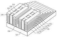
도 1a를 참조하면, 본 발명 실시예의 불휘발성 메모리 소자(1)는 메모리 셀들이 포함되는 셀 영역(2)과, 메모리 셀들을 동작시키는 주변 회로가 포함되는 주변 영역(3)을 포함할 수 있다.Referring to FIG. 1A, a
셀 영역(2)은 반도체 기판(20) 상에서 Z 방향으로 수직 적층되고 X-Y 평면을 이루는 플레이트 형상의 복수개의 컨트롤 게이트(27), 복수개의 컨트롤 게이트(27)의 아래에 제공된 하부 선택 게이트(23), 복수개의 컨트롤 게이트(27)의 위에 제공된 복수개의 상부 선택 게이트(25)와, 상부 선택 게이트(25) 상에 적층되고 Y 방향으로 연장된 복수개의 비트라인(21), 그리고 반도체 기판(20) 상에서 Z 방향으로 수직 연장된 복수개의 활성 기둥(29: active pillar)을 포함할 수 있다. 복수개의 활성 기둥(29) 각각은 반도체 기판(20)에서부터 비트라인(21)까지 연장되어 상하부 선택 게이트(23,25)와 컨트롤 게이트(27)를 관통하도록 제공되어 채널로 사용될 수 있다. 반도체 기판(20)은 P형 실리콘 기판일 수 있다. 활성 기둥(29)은 반도체 기판(20)과 동일 유사한 물질로 구성되고, 동일한 도전형일 수 있다. 반도체 기판(20)은 반대 도전형, 가령 N형의 소오스(20s)를 포함할 수 있다.The
주변 영역(3)은 복수개의 상부 선택 게이트(25)를 상부 선택라인 구동회로에 연결하는 복수개의 제1 라인(32)과, 복수개의 컨트롤 게이트(27)를 워드라인 구동회로에 연결하는 복수개의 제2 라인(33)과, 하부 선택 게이트(23)를 하부 선택라인 구동회로에 연결하는 제3 라인(34)을 포함할 수 있다. 복수개의 제1 라인들(32)과 복수개의 상부 선택 게이트(25) 사이에는 이들을 전기적으로 연결하는 복수개의 제1 콘택 플러그(32a)가 제공되고, 복수개의 제2 라인(33)과 복수개의 컨트롤 게이트(27) 사이에는 이들을 전기적으로 연결하는 복수개의 제2 콘택 플러그(33a)가 제공되고, 제3 라인(34)과 하부 선택 게이트(23) 사이에는 이들을 전기적으로 연결하는 제3 콘택 플러그(34a)가 제공될 수 있다.The
하부 선택 게이트(23)와 상부 선택 게이트(25) 중 어느 하나는 X-Y 평면을 이루는 플레이트 형태로 제공될 수 있고 다른 하나는 X 방향으로 연장된 분리형의 라인 형태로 제공될 수 있다. 다른 예로, 하부 선택 게이트(23)와 상부 선택 게이트(25) 각각은 X 방향으로 연장된 분리형의 라인 형태로 제공될 수 있다. 본 실시예에 의하면 하부 선택 게이트(23)는 X-Y 평면을 이루는 플레이트 형태이고, 상부 선택 게이트(25)는 X 방향으로 연장된 분리형의 라인 형태일 수 있다.One of the lower
게이트들(23,25,27)은 계단형 구조로 제공될 수 있다. 상기 계단형 구조로 말미암아 복수개의 제3 콘택 플러그(34a)를 복수개의 컨트롤 게이트(27)에 각각 연결되는 영역을 제공하는 복수개의 워드라인 패드(37)가 정의될 수 있다. 본 명세서에서 워드라인 패드(37)는 하층 컨트롤 게이트(27) 중에서 상층 컨트롤 게이트(27)에 의해 덮히지 않아 노출된 표면으로 정의할 수 있다. 상기 계단형 구조는 컨트롤 게이트(27)의 좌우 양측에 구현될 수 있다.
The
도 1b는 도 1a의 셀 영역을 도시한 사시도이고, 도 1c 및 1d는 도 1b의 메모리 트랜지스터를 도시한 사시도이다.FIG. 1B is a perspective view illustrating the cell region of FIG. 1A, and FIGS. 1C and 1D are perspective views illustrating the memory transistor of FIG. 1B.
도 1b를 참조하면, 활성 기둥(29)과 컨트롤 게이트(27)는 메모리 트랜지스터(28)를 정의하고, 활성 기둥(29)과 하부 선택 게이트(23)는 하부 선택 트랜지스터(24)를 정의하고, 활성 기둥(29)과 상부 선택 게이트(25)는 상부 선택 트랜지스터(26)를 정의할 수 있다. 본 실시예의 불휘발성 메모리 소자(1)는 하나의 활성 기둥(29)에 형성된 복수개의 메모리 트랜지스터(28)와 상하부 트랜지스터(26,24)가 직렬로 연결되어 하나의 셀 스트링(22)을 구성하는 낸드 플래시(NAND Flash) 메모리 소자일 수 있다. 본 실시예에서 하나의 셀 스트링(22)은 4개의 메모리 트랜지스터(28)를 가지는데, 하나의 셀 스트링(22)의 메모리 트랜지스터(28)의 수는 이에 한정되지 아니하며 메모리 용량에 의존하여 임의의 갯수, 가령 8개, 16개, 32개 등일 수 있다. 활성 기둥(29)은 그 단면이 원형인 원기둥 형상일 수 있고, 또는 그 단면이 사각형인 사각기둥 형상 등 그 기둥 형상은 임의적일 수 있다.Referring to FIG. 1B, the
메모리 트랜지스터(28) 및 상하부 선택 트랜지스터(26,24)는 활성 기둥(29)에 소오스/드레인이 존재하지 않는 이른바 공핍형(depletion) 트랜지스터로 제공될 수 있다. 다른 예로, 메모리 트랜지스터(28) 및 상하부 선택 트랜지스터(26,24)는 활성 기둥(29)에 소오스/드레인이 존재하는 이른바 증가형(enhancement) 트랜지스터로 제공될 수 있다. The
복수개의 활성 기둥(29)은 복수개의 컨트롤 게이트(27)를 관통하는 Z 방향의 축을 갖고, 이에 따라 복수개의 컨트롤 게이트(27)와 복수개의 활성 기둥(29) 사이의 교점들은 3차원적으로 분포될 수 있다. 본 발명 실시예의 메모리 트랜지스터(28)는 이러한 3차원적으로 분포된 교점들에 각각 형성될 수 있다.The plurality of
도 1c를 참조하면, 활성 기둥(29)과 컨트롤 게이트(27) 사이에는 전하저장막을 포함하는 게이트 절연막(30)이 배치될 수 있다. 전하저장막은 전하를 트랩할 수 있는 절연막을 포함할 수 있다. 예를 들어, 게이트 절연막(30)이 실리콘 산화막과 실리콘 질화막(또는 실리콘 산화질화막)과 실리콘 산화막이 적층된 이른바 오엔오(ONO)막인 경우 전하는 실리콘 질화막(또는 실리콘 산화질화막)에 트랩되어 유지될 수 있다. 다른 예로, 전하저장막은 전도체로 구성된 플로팅 게이트를 포함할 수 있다.Referring to FIG. 1C, a
도 1d를 참조하면, 활성 기둥(29)은 그 내부에 절연체(39)을 갖는 이른바 마카로니(macaroni) 형태일 수 있다. 절연체(39)는 기둥 모양일 수 있다. 절연체(39)가 활성 기둥(29)의 내부를 차지하므로 활성 기둥(29)은 도 1c의 구조에 비해 더 얇은 두께를 가질 수 있고, 이는 캐리어의 트랩 싸이트(trap site)를 줄일 수 있다.Referring to FIG. 1D, the
도 1b를 다시 참조하면, 상하부 선택 트랜지스터(26,24)는 도 1c 혹은 1d에 도시된 바와 동일 유사한 구조를 가질 수 있다. 상하부 선택 트랜지스터(26,24)의 게이트 절연막(30)은 실리콘 산화막이나 실리콘 질화막으로 구성될 수 있다.
Referring back to FIG. 1B, the top and bottom
도 1e는 본 발명의 실시예에 따른 불휘발성 메모리 소자를 도시한 등가회로도이다.1E is an equivalent circuit diagram illustrating a nonvolatile memory device according to an embodiment of the present invention.
도 1e를 도 1a와 같이 참조하면, 본 발명 실시예의 불휘발성 메모리 소자(1)에 있어서 복수개의 컨트롤 게이트(27)는 복수개의 워드라인(WL0-WL3)에 상당하고, 복수개의 상부 선택 게이트(25)는 복수개의 스트링 선택라인(SSL0-SSL2)에 상당하고, 하부 선택 게이트(23)는 접지 선택라인(GSL)에 상당하고, 반도체 기판(20)의 소오스(20s)는 공통 소오스 라인(CSL)에 상당한다. 셀 스트링(22)은 복수개의 비트라인(BL0-BL2) 각각에 복수개 연결될 수 있다.Referring to FIG. 1E as shown in FIG. 1A, in the
복수개의 컨트롤 게이트(27) 각각은 2차원적으로 펼쳐져 있는 평판형 구조를 이룰 수 있으므로 복수개의 워드라인(WL0-WL3) 각각은 평면 구조를 가지며 셀 스트링(22)에 대해 실질적으로 수직일 수 있다. 복수개의 워드라인(WL0-WL3)에는 복수개의 메모리 트랜지스터(28)가 3차원적으로 분포될 수 있다.Since each of the plurality of
상부 선택 게이트(25)는 X 방향으로 연장된 분리형 배선 구조를 이룰 수 있으므로 복수개의 스트링 선택라인(SSL0-SSL2)은 복수개의 비트라인(BL0-BL2)을 X 방향으로 가로지도록 배치될 수 있다. Y 방향으로 배열된 복수개의 스트링 선택라인(SSL0-SSL2) 각각은 X 방향으로 배열된 복수개의 비트라인(BL0-BL2) 각각과 전기적으로 연결되므로 하나의 셀 스트링(22)이 독립적으로 선택될 수 있다.Since the upper
하부 선택 게이트(23)는 2차원적으로 펼쳐져 있는 평판평 구조를 이룰 수 있으므로 접지 선택라인(GSL)은 평면 구조를 가지며 셀 스트링(22)에 대해 실질적으로 수직일 수 있다. 접지 선택라인(GSL)은 활성 기둥(29)과 반도체 기판(20) 사이의 전기적 연결을 제어할 수 있다.Since the
본 실시예의 불휘발성 메모리 소자(1)에 있어서 프로그램 동작은 선택된 워드라인(WL)과 활성 기둥(29) 사이에 전압차를 설정하여 전하를 전하저장막에 주입함으로써 구현될 수 있다. 일례로, 선택된 워드라인(WL)에 프로그램 전압(Vprog)을 인가하므로써 파울러-노던하임 터널링 현상을 이용하여 활성 기둥(29)으로부터 프로그램하고자 하는 워드라인(WL)에 속한 메모리 트랜지스터(28)의 전하저장막으로 전자를 주입하여 프로그램을 구현할 수 있다. 선택된 워드라인(WL)에 인가된 프로그램 전압은 비선택 워드라인에 속한 메모리 트랜지스터를 프로그램시킬 수 있으므로, 부스팅 기술을 이용하여 의도되지 않는 프로그램을 방지할 수 있다.In the
판독 동작은 판독하고자 하는 메모리 트랜지스터(28)가 연결된 워드라인(WL)에 가령 O 볼트(volt)로 설정하고 다른 워드라인(WL)에는 읽기 전압(Vread)을 설정한다. 그 결과, 판독하고자 하는 메모리 트랜지스터(28)의 문턴 전압(Vth)이 0 볼트보다 큰지 또는 작은지에 의존하여 비트라인(BL)에 전류가 충전되는지가 결정되며, 이에 따라 비트라인(BL)의 전류를 감지하므로써 판독하고자 하는 메모리 트랜지스터(28)의 데이터 정보가 판독될 수 있다.The read operation is set to, for example, O volts in a word line WL to which the
소거 동작은 게이트 유도 드레인 누설전류(GIDL)를 이용하여 블록 단위로 수행될 수 있다. 일례로, 선택된 비트라인(BL)과 기판(20)에 소거 전압(Verase)을 인가하므로써 활성 기둥(29)의 전위를 상승시킨다. 이때, 활성 기둥(29)의 전위는 약간 지연되면서 상승되도록 할 수 있다. 이에 수반하여, 하부 선택 게이트(23)의 단자에서 GIDL이 발생하고, GIDL에 의해 생성된 전자는 기판(20)으로 방출되고 생성된 정공은 활성 기둥(29)으로 방출된다. 이로 인해 소거 전압(Verase) 근처의 전위가 메모리 트랜지스터(28)의 채널, 즉 활성 기둥(29)으로 전달될 수 있다. 이때, 워드라인(WL)의 전위를 O 볼트로 설정하면 메모리 트랜지스터(28)에 축적된 전자들이 빠져나오게 되어 데이터 소거가 구현될 수 있다. 한편, 의도되지 않은 소거 동작이 행해지지 않도록 비선택 블록의 워드라인을 플로팅시킬 수 있다.The erase operation may be performed in units of blocks by using the gate induced drain leakage current GIDL. For example, the potential of the
본 실시예에 따른 불휘발성 메모리 소자(1)의 동작 방법은 본 발명의 기술적 사상을 예시적으로 설명하기 위한 것이며, 본 발명의 기술적 특징이 이에 한정되는 것은 아니다. 이 분야에 종사하는 통상의 지식을 가진 자라면 공지된 기술들에 기초하여 상기 동작 방법의 변형을 용이하게 구현하는 것은 자명하므로, 동작 방법과 관련된 본 발명의 기술적 특징은 공지된 기술들에 기초하여 다양하게 변형되어 구현될 수 있음은 물론이다.
The operation method of the
도 2a 내지 2h는 본 발명의 실시예에 따른 불휘발성 메모리 소자의 제조방법을 도시한 사시도이다. 상기 도면들에서 편의상 절연막의 도시를 생략하였다.2A to 2H are perspective views illustrating a method of manufacturing a nonvolatile memory device according to an embodiment of the present invention. In the drawings, the insulating film is omitted for convenience.
도 2a를 참조하면, 반도체 기판(20)을 제공할 수 있다. 반도체 기판(20)은 가령 P형 단결정 실리콘 웨이퍼일 수 있다. 반도체 기판(20)은 활성 영역(20a)을 정의하는 소자분리막(미도시)을 포함할 수 있다. 활성 영역(20a)은 소오스(20s)를 포함할 수 있다. 소오스(20s)는 N형일 수 있다.Referring to FIG. 2A, a
도 2b를 참조하면, 반도체 기판(20) 상에 하부 선택 게이트(23)를 형성할 수 있다. 하부 선택 게이트(23)는 도전성 물질, 가령 다결정 실리콘 혹은 금속을 증착하여 형성할 수 있다. 하부 선택 게이트(23)는 플레이트 혹은 라인 형태로 구현될 수 있다. 본 실시예에 의하면 하부 선택 게이트(23)는 다결정 실리콘을 증착하여 플레이트 형태로 형성할 수 있다. 하부 선택 게이트(23)를 관통하여 반도체 기판(20)과 전기적으로 연결되는 복수개의 제1 기둥(29a)을 증착 혹은 에피택시얼 공정으로 형성할 수 있다. 제1 기둥(29a)은 가령 드라이 에칭으로 하부 선택 게이트(23)를 관통하여 반도체 기판(20)을 개방하는 홀을 형성하고, 그 홀을 전도체로 매립하여 형성할 수 있다. 제1 기둥(29a)은 그 단면이 원형, 타원형, 다각형 등 임의의 형태일 수 있다. 제1 기둥(29a)은 반도체 기판(20)과 동일 유사한 물질로 형성할 수 있다. 일례로, 제1 기둥(29a)은 비정질, 단결정 혹은 다결정 실리콘으로 형성할 수 있다. 제1 기둥(29a)과 하부 선택 게이트(23) 사이에는 제1 게이트 절연막이 형성될 수 있고, 이에 따라 도 1c에 도시된 바와 동일 유사한 구조가 구현될 수 있다. 제1 게이트 절연막은 가령 실리콘 산화막이나 실리콘 질화막을 증착하여 형성할 수 있다.Referring to FIG. 2B, the
도 2c를 참조하면, 하부 선택 게이트(23) 상에 복수개의 컨트롤 게이트(27)를 형성할 수 있다. 컨트롤 게이트(27)는 하부 선택 게이트(23)와 동일 유사한 물질로 형성할 수 있다. 일례로, 컨트롤 게이트(27)는 다결정 실리콘을 증착하여 플레이트 형태로 형성할 수 있다. 복수개의 컨트롤 게이트(27)는 동일한 두께를 가지도록 형성할 수 있다. 컨트롤 게이트(27)는 하부 선택 게이트(23)와 동일하거나 혹은 다른 두께를 가질 수 있다. 복수개의 컨트롤 게이트(27)를 관통하여 복수개의 제1 기둥(29a)과 연결되는 복수개의 제2 기둥(29b)을 증착 혹은 에피택시얼 공정으로 형성할 수 있다. 제2 기둥(29b)은 가령 드라이 에칭으로 복수개의 컨트롤 게이트(27)를 관통하여 제1 기둥(29a)을 개방하는 홀을 형성하고, 그 홀을 전도체로 매립하여 형성할 수 있다. 제2 기둥(29b)은 제1 기둥(29a)과 동일 유사한 물질로 형성할 수 있다. 일례로, 제2 기둥(29b)은 단결정 혹은 다결정 실리콘으로 형성할 수 있다. 다른 예로, 제2 기둥(29b)은 비정질, 단결정 혹은 다결정 실리콘막 내에 절연막이 형성된 도 1d에 도시된 바와 같은 마카로니 구조로 형성할 수 있다. 제2 기둥(29b)과 컨트롤 게이트(27) 사이에는 전하저장막이 포함된 제2 게이트 절연막이 형성될 수 있고, 이에 따라 도 1c 혹은 1d에 도시된 바와 동일 유사한 구조가 구현될 수 있다. 제2 게이트 절연막은 실리콘 산화막, 실리콘 질화막 또는 실리콘 산화질화막, 실리콘 산화막 등을 차례로 증착하여 3중 박막 구조로 형성할 수 있다. 제2 게이트 절연막에 있어서 실리콘 질화막 또는 실리콘 산화질화막은 전하를 트랩하여 정보를 저장하는 전하저장막으로 사용되고, 2개의 실리콘 산화막 중 어느 하나는 블록킹 절연막으로 사용되고 다른 하나는 터널 절연막으로 사용될 수 있다. 다른 예로, 전하저장막은 실리콘 질화막을 대신하여 다결정 실리콘과 같은 전도체로 구성된 플로팅 게이트로 대체될 수 있다. 또 다른 예로, 터널 절연막은 실리콘 질화막 혹은 실리콘 산화막/실리콘 질화막으로 형성하고, 블록킹 절연막은 실리콘 질화막, 실리콘 산화막/실리콘 질화막, 알루미늄 산화막, 혹은 이들의 조합으로 형성할 수 있다.Referring to FIG. 2C, a plurality of
도 2d를 참조하면, 복수개의 컨트롤 게이트(27)를 계단형 구조로 형성할 수 있다. 이에 따라, 복수개의 컨트롤 게이트(27) 각각에는 워드라인 패드(37)가 정의될 수 있다. 상기 계단형 구조의 구현에 의해 하부 선택 게이트(23)에는 하부 선택라인 패드(38)가 정의될 수 있다. 상기 계단형 구조의 구현은 도 3a 내지 3l을 참조하여 설명한다.
Referring to FIG. 2D, a plurality of
도 3a 내지 3l은 본 발명의 실시예에 따른 계단형 구조를 구현할 수 있는 패터닝 방법을 도시한 사시도이다.3A to 3L are perspective views illustrating a patterning method capable of implementing a stepped structure according to an embodiment of the present invention.
도 3a를 참조하면, 하부 선택 게이트(23) 상에 복수개의 절연막(47)과 복수개의 컨트롤 게이트(27)를 번갈아 형성할 수 있다. 복수개의 컨트롤 게이트(27)는 플레이트 형태로 형성할 수 있다. 구분 편의상 복수개의 컨트롤 게이트(27)를 부호 27_1 내지 27_4로 표지하기로 한다. 유사하게, 복수개의 절연막(47)을 부호 47_1 내지 47_4로 표지하기로 한다. 제1 컨트롤 게이트(27_1) 상에 포토 공정으로 가령 포토레지스트로 구성된 제1 마스크(50)를 형성할 수 있다. 제1 마스크(50)는 제1 컨트롤 게이트(27_1)의 센터를 가로지르는 형태를 가지도록 형성될 수 있다.Referring to FIG. 3A, a plurality of insulating
도 3b를 참조하면, 제1 마스크(50)를 이용한 제1 패드 에칭으로 제1 컨트롤 게이트(27_1)를 패터닝할 수 있다. 제1 패드 에칭에 의해 제1 절연막(47_1)도 같이 패터닝되어 제2 컨트롤 게이트(27_2)가 드러날 수 있다. 제1 패드 에칭은 드라이 에칭을 사용할 수 있다. 제1 컨트롤 게이트(27_1)의 양측 가장자리 상면은 제1 워드라인 패드(37_1)로 정의된다.Referring to FIG. 3B, the first control gate 27_1 may be patterned by first pad etching using the
도 3c를 참조하면, 제2 컨트롤 게이트(27_2) 상에 제1 제1 마스크(50)를 덮는 제1 막(52)을 형성할 수 있다. 제1 막(52)은 폴리머를 증착하여 형성할 수 있다. 일례로, C-H-F를 포함하는 가스, N2 및 Ar을 포함하는 플라즈마를 이용하는 증착 공정으로 제1 막(52)을 형성할 수 있다. 제1 막(52)은 폴리머, 가령 C 및 H를 포함하는 카본중합체로 구성될 수 있다.Referring to FIG. 3C, a
도 3d를 참조하면, 스페이서 에칭으로 제1 막(52)의 일부를 제거하여 제1 마스크(50)의 양측벽에 제1 스페이서(52s)를 형성한다. 제1 마스크(50)와 제1 스페이서(52s)가 제2 마스크(60)를 이룬다. 상기 스페이서 에칭은 제1 막(52)의 형성에 소요된 가스를 포함하는 플라즈마를 이용할 수 있다. 일례로, C-H-F를 포함하는 가스, N2 및 Ar을 포함하는 플라즈마를 이용하는 드라이 에칭 공정으로 제1 막(52)을 스페이서 에칭하여 제1 스페이서(52s)를 구현할 수 있다.Referring to FIG. 3D, a portion of the
도 3c의 폴리머 증착 공정과 도 3d의 폴리머 에칭 공정은 동일한 플라즈마를 이용할 수 있다. 따라서, 상기 폴리머 증착 및 폴리머 에칭 공정은 인시튜(In-situ)로 진행하는 것이 가능하며, 더 나아가 게이트들(23,27)의 증착 및 패드 에칭 공정과 인시튜로 진행하는 것이 가능하다. 동일한 플라즈마로써 폴리머 증착과 폴리머 에칭 공정을 인시튜로 진행하는 경우 공정 조건을 다르게 가져가는 것이 효과적인 증착과 에칭을 구현하는데 바람직하다. 효과적인 폴리머 증착 및 폴리머 에칭을 구현하기 위해, C-H-F를 포함하는 가스 중에서 C와 H, 적어도 C는 폴리머 증착에 관여하고 F는 폴리머 에칭에 관여하므로, 폴리머 증착 공정에선 C 및 H, 혹은 C 성분을 F 성분에 비해 높게 설정하고, 폴리머 증착 공정에선 그 반대로 설정할 수 있다. 일례로, 도 3c의 폴리머 증착 공정에선 메틸플로라이드(CH3F)를 제공하고, 도 3d의 폴리머 에칭 공정에선 트리플루오로메탄(CHF3), 카본테트라플로라이드(CF4) 혹은 이의 조합을 제공할 수 있다. 더 효과적인 폴리머 에칭 공정을 위해 O2가 더 제공될 수 있다. 선택적으로 컨트롤 게이트(27)쪽에 파워를 걸어 에천트의 직진성을 높이는 것도 더 효과적인 폴리머 에칭 공정을 구현하는데 바람직하다.The polymer deposition process of FIG. 3C and the polymer etching process of FIG. 3D may use the same plasma. Accordingly, the polymer deposition and polymer etching process may proceed in-situ, and further, may proceed in-situ with the deposition and pad etching processes of the
도 3e를 참조하면, 제2 마스크(60)를 이용한 제2 패드 에칭으로 제2 컨트롤 게이트(27_2) 및 제2 절연막(47_2)을 패터닝할 수 있다. 이에 따라 제2 컨트롤 게이트(27_2)의 양측 가장자리 상면은 일정한 너비를 갖는 제2 워드라인 패드(37_2)로 정의될 수 있다. 제2 워드라인 패드(37_2)의 너비는 제1 스페이서(52s)의 제1 너비(W1)에 의존한다. 따라서, 도 3c의 폴리머 증착 공정에 의해 형성된 제1 막(52)의 두께를 적절히 조절하므로써 제2 워드라인 패드(37_2)의 너비를 결정할 수 있다.Referring to FIG. 3E, the second control gate 27_2 and the second insulating layer 47_2 may be patterned by the second pad etching using the
도 3f 내지 3h를 참조하면, 도 3c 내지 3e를 참조하여 설명한 바와 동일 유사한 공정을 이용하여, 플라즈마를 이용한 폴리머 증착 공정으로 제2 마스크(60)를 덮는 제2 막(54)을 폴리머로 형성하고(도 3f), 상기 플라즈마를 이용한 스페이서 에칭 공정으로 제2 막(54)의 일부를 제거하므로써 제2 마스크(60)의 양측벽에 제2 스페이서(54s)를 형성하여 제3 마스크(70)를 정의하고(도 3g), 제3 마스크(70)를 이용한 제3 패드 에칭으로 제3 컨트롤 게이트(27_3) 및 제3 절연막(47_3)을 일부 제거하여 제3 컨트롤 게이트(27_3)의 양측 가장자리 상면을 제3 워드라인 패드(37_3)로 정의할 수 있다(도 3h). 제3 워드라인 패드(37_3)의 너비는 제2 스페이서(54s)의 제2 너비(W2)에 의존한다. Referring to FIGS. 3F to 3H, a
도 3i 내지 3k를 참조하면, 도 3c 내지 3e를 참조하여 설명한 바와 동일 유사한 공정을 이용하여, 플라즈마를 이용한 폴리머 증착 공정으로 제3 마스크(70)를 덮는 제3 막(56)을 폴리머로 형성하고(도 3i), 상기 플라즈마를 이용한 스페이서 에칭 공정으로 제3 막(56)의 일부를 제거하므로써 제3 마스크(70)의 양측벽에 제3 스페이서(56s)를 형성하여 제4 마스크(80)를 정의하고(도 3j), 제4 마스크(80)를 이용한 제4 패드 에칭으로 제4 컨트롤 게이트(27_4) 및 제4 절연막(47_4)을 일부 제거하여 제4 컨트롤 게이트(27_4)의 양측 가장자리 상면을 제4 워드라인 패드(37_4)로 정의할 수 있다(도 3k). 제4 워드라인 패드(37_4)의 너비는 제3 스페이서(56s)의 제3 너비(W3)에 의존한다. 도 3k에 도시된 바와 같이, 상기 제4 패드 에칭에 의해 하부 선택 게이트(23)의 양측 가장자리 상면이 노출되는데 그 상면을 하부 선택라인 패드(38)로 정의할 수 있다.3I to 3K, a
도 3l을 참조하면, 제4 마스크(80)를 애싱 공정으로 제거할 수 있다. 상기 일련의 공정에 의하면 계단형 구조를 가지며, 복수개의 워드라인 패드(37)를 갖는 수직 적층된 복수개의 컨트롤 게이트(27)가 구현될 수 있다. 절연막(47) 역시 계단형 구조로 패터닝될 수 있다.Referring to FIG. 3L, the
상기 계단형 구조를 구현할 수 있는 패터닝 방법에 의하면, 제1 마스크(50)의 양측벽에 제1 스페이서(52s)를 부착하는 것이므로 제1 마스크(50)의 수축이나 팽창을 유발하지 아니하며, 이러한 것은 제2 스페이서(54s) 및 제3 스페이서(56s) 부착의 경우에 동일 유사하게 적용될 수 있다. 따라서, 제1 내지 제3 스페이서(52s,54s,56s)의 제1 내지 제3 너비(W1-W3)를 원하는 치수, 그리고 균일하게 설정할 수 있으므로 복수개의 워드라인 패드(37)의 너비를 균일하게 형성할 수 있다. 더군다나, 상기 패터닝 방법은 1회의 포토 공정으로 제1 마스크(50)를 형성한 후 폴리머 증착 및 폴리머 에칭으로 다수 단(가령, 16단)의 계단형 구조를 형성할 수 있다.According to the patterning method capable of implementing the stepped structure, since the
상기 패터닝 방법에 있어서 스페이서(52s-56s) 물질은 폴리머에 한정되지 아니하고, 절연막(47)과 식각 선택비가 있는 물질, 가령 실리콘 산화막, 실리콘 질화막, 실리콘 카바이드 혹은 이들의 조합을 선택할 수 있다. 다른 예로, 스페이서(52s-56s) 물질로서 금속, 금속 산화막, 금속 질화막 등도 선택할 수 있다. 상기 패터닝 방법은 계단형 구조의 컨트롤 게이트(27)를 구현하는 것에 한정되지 아니하고, 도전막들을 비롯한 전극들이 적층된 계단형 구조를 구현하는데 널리 쓰일 수 있다.
In the patterning method, the material of the
도 2e를 참조하면, 게이트들(23,27)을 가로지르는 슬릿(19)을 형성할 수 있다. 슬릿(19)에 의해 게이트들(23,27)은 양분되어 반도체 기판(20) 상에는 2 개의 소자가 구현될 수 있다. 최상층의 컨트롤 게이트(27) 상에 복수개의 상부 선택 게이트(25)를 형성할 수 있다. 상부 선택 게이트(25)는 플레이트 혹은 라인 형태로 형성할 수 있다. 본 실시예에 의하면 상부 선택 게이트(25)는 라인 형태로 형성할 수 있다. 상부 선택 게이트(25)는 컨트롤 게이트(27) 및/또는 하부 선택 게이트(23)와 동일 유사한 물질, 가령 다결정 실리콘으로 형성할 수 있다. 하나의 선택 게이트(25)는 그 길이 방향으로 늘어선 복수개의 제2 기둥(29b)과 공통으로 연결될 수 있다.Referring to FIG. 2E, a
도 2f를 참조하면, 상부 선택 게이트(25)를 관통하여 복수개의 제2 기둥(29b)과 연결되는 복수개의 제3 기둥(29c)을 증착 혹은 에피택시얼 공정으로 형성할 수 있다. 제3 기둥(29c)은 가령 드라이 에칭으로 상부 선택 게이트(25)를 관통하여 제2 기둥(29b)을 개방하는 홀을 형성하고, 그 홀을 전도체로 매립하여 형성할 수 있다. 제3 기둥(29c)은 제1 기둥(29a) 및/또는 제2 기둥(29b)과 동일 유사한 물질로 형성할 수 있다. 일례로, 제3 기둥(29c)은 비정질, 단결정 혹은 다결정 실리콘으로 형성할 수 있다. 제3 기둥(29c)과 상부 선택 게이트(25) 사이에는 제3 게이트 절연막이 형성될 수 있고, 이에 따라 도 1c에 도시된 바와 동일 유사한 구조가 구현될 수 있다. 제3 게이트 절연막은 가령 실리콘 산화막이나 실리콘 질화막을 증착하여 형성할 수 있다. 제1 내지 제3 기둥(29a-29c)은 상하 연결되어 활성 기둥(29)을 이룬다. 제1 내지 제3 기둥(29a-29c)은 반도체 기판(20)과 동일한 도전형, 가령 P형을 가지도록 형성될 수 있다. 따라서, 반도체 기판(20)과 활성 기둥(29)은 등전위를 가질 수 있다.Referring to FIG. 2F, a plurality of
도 2g를 참조하면, 활성 기둥(29)과 연결되는 복수개의 비트라인(21)을 형성할 수 있다. 하나의 비트라인(21)은 그 길이 방향으로 늘어선 복수개의 활성 기둥(29)과 공통으로 연결될 수 있다. 비트라인(21)의 신장 방향과 상부 선택 게이트(23)의 신장 방향은 서로 교차, 가령 직교할 수 있다. 따라서, 복수개의 비트라인(21)과 복수개의 상부 선택 게이트(25)은 서로 가로지도록 배치될 수 있다. 복수개의 비트라인(21) 중 어느 하나와 복수개의 상부 선택 게이트(25) 중 어느 하나에 의해 하나의 셀 스트링(22)이 정의될 수 있다. 활성 기둥(29) 중 비트라인(21)에 인접한 영역에 드레인이 형성될 수 있다. 활성 기둥(29)과 비트라인(21) 사이에 플러그를 더 형성할 수 있다.Referring to FIG. 2G, a plurality of
도 2h를 참조하면, 복수개의 상부 선택 게이트(25) 상에 복수개의 제1 콘택 플러그(32a)를 형성하고, 복수개의 제1 콘택 플러그(32a)에 연결되는 복수개의 제1 라인(32)을 형성할 수 있다. 제1 라인(32)은 상부 선택 게이트(25)를 상부 선택라인 구동회로에 전기적으로 연결시킬 수 있다. 복수개의 워드라인 패드(37) 상에 복수개의 제2 콘택 플러그(33a)를 형성하고, 복수개의 제2 콘택 플러그(33a)에 연결되는 복수개의 제2 라인(33)을 형성할 수 있다. 제2 라인(34)은 컨트롤 게이트(27)를 워드라인 구동회로에 전기적으로 연결시킬 수 있다. 하부 선택 게이트(23)의 하부 선택라인 패드(38) 상에 제3 콘택 플러그(34a)를 형성하고, 제3 콘택 플러그(34a)에 연결되는 제3 라인(34)을 형성할 수 있다. 제3 라인(34)은 하부 선택 게이트(23)를 하부 선택라인 구동회로에 전기적으로 연결시킬 수 있다. 제1 내지 제3 콘택 플러그(32a,33a,34a)는 금속을 증착하여 동시에 형성할 수 있다. 유사하게, 제1 내지 제3 라인(32,33,34)은 금속을 증착하여 동시에 형성할 수 있다. 상기 일련의 공정에 의해 계단형 구조의 컨트롤 게이트(27)를 갖는 불휘발성 메모리 소자(1)가 구현될 수 있다.
Referring to FIG. 2H, a plurality of first contact plugs 32a are formed on the plurality of
도 4a는 본 발명의 다른 실시예에 따른 불휘발성 메모리 소자를 도시한 사시도이고, 도 4b 및 4c는 본 발명의 다른 실시예에 따른 불휘발성 메모리 소자의 제조방법에 있어서 계단형 구조를 구현하는 방법을 도시한 사시도이다.4A is a perspective view illustrating a nonvolatile memory device according to another embodiment of the present invention, and FIGS. 4B and 4C illustrate a stepped structure in a method of manufacturing a nonvolatile memory device according to another embodiment of the present invention. It is a perspective view showing.
도 4a를 참조하면, 본 다른 실시예의 불휘발성 메모리 소자(1a)는 제2 콘택 플러그(33a)가 형성되는 일측에 계단형 구조를 가지는 적층된 복수개의 컨트롤 게이트(27a)를 포함할 수 있다. 이외는 도 1a에 도시된 불휘발성 메모리 소자(1)와 동일 유사하게 구성될 수 있다.Referring to FIG. 4A, the
도 4b 및 4c를 참조하면, 도 3a 내지 3l을 참조하여 설명한 바와 동일 유사한 공정으로 일측에 계단형 구조를 갖는 컨트롤 게이트(27a)를 형성할 수 있다. 일례로, 도 4b에 도시된 바와 같이 하부 선택 게이트(23) 상에 복수개의 컨트롤 게이트(27a)와 복수개의 절연막(47a)을 플레이트 형태로 번갈아 형성하고, 최상층의 컨트롤 게이트(27a) 상면 중에서 일측에 한정된 제1 마스크(50)를 형성할 수 있다. 폴리머 증착 및 폴리머 에칭으로 제1 마스크(50)의 일측벽에 스페이서를 형성한 후 패드 에칭하고 이러한 과정을 반복하므로써 도 4c에 도시된 바와 같은 계단형 구조를 갖는 컨트롤 게이트(27a)를 형성할 수 있다. 상기 일측에 계단형 구조를 갖는 컨트롤 게이트(27a)를 형성하는 공정은 후술한 다른 실시예들에도 적용될 수 있다.
4B and 4C, a
도 5a는 본 발명의 또 다른 실시예에 따른 불휘발성 메모리 소자를 도시한 사시도이고, 도 5b 및 5c는 본 발명의 또 다른 실시예에 따른 불휘발성 메모리 소자의 제조방법에 있어서 계단형 구조를 구현하는 방법을 도시한 사시도이다.5A is a perspective view illustrating a nonvolatile memory device according to still another embodiment of the present invention, and FIGS. 5B and 5C illustrate a stepped structure in a method of manufacturing a nonvolatile memory device according to still another embodiment of the present invention. It is a perspective view showing the method.
도 5a를 참조하면, 본 또 다른 실시예의 불휘발성 메모리 소자(1b)는 전후좌우 네측에 계단형 구조를 가지는 피라미드 형태로 적층된 복수개의 컨트롤 게이트(27b)를 포함할 수 있다. 제2 콘택들(33a)은 컨트롤 게이트(27b)의 우측 워드라인 패드(37a) 및 전방 워드라인 패드(37b)에 분산되어 형성될 수 있다. 컨트롤 게이트(27b)의 우측에 제2 라인들(33)을 모두 형성하기에 곤란한 문제점이 있을 수 있다. 가령 컨트롤 게이트(27b)의 갯수가 많은 경우 컨트롤 게이트(27b)의 우측에 모든 제2 라인들(33)을 형성할 수 있는 영역이 충분히 확보되지 않은 경우 제2 라인들(33) 중 일부를 컨트롤 게이트(27b)의 전방에 형성하므로써 상기 곤란한 점을 제거할 수 있다. 이외는 도 1a에 도시된 불휘발성 메모리 소자(1)와 동일 유사하게 구성될 수 있다.Referring to FIG. 5A, the
도 5b 및 5c를 참조하면, 도 3a 내지 3l을 참조하여 설명한 바와 동일 유사한 공정을 진행하여 모든 측면이 계단형 구조를 가지는 피라미드형 컨트롤 게이트(27b)를 구현할 수 있다. 일례로, 도 5b에 도시된 바와 같이 하부 선택 게이트(23) 상에 복수개의 컨트롤 게이트(27b)와 복수개의 절연막(47b)을 플레이트 형태로 번갈아 형성하고, 최상층의 컨트롤 게이트(27a) 상면 중에서 에지에 둘러싸인 센터에 한정된 제1 마스크(50)를 형성할 수 있다. 폴리머 증착 및 폴리머 에칭으로 제1 마스크(50)의 네측벽에 스페이서를 형성한 후 패드 에칭하는 과정을 반복하므로써 도 5c에 도시된 바와 같은 피라미드형 컨트롤 게이트(27b)를 형성할 수 있다. 상기 피리미드형 컨트롤 게이트(27b)를 형성하는 공정은 후술한 다른 실시예들에도 적용될 수 있다.
5B and 5C, a similar process as described with reference to FIGS. 3A to 3L may be performed to implement a
도 6a 내지 6m은 본 발명의 변형 실시예에 따른 불휘발성 메모리 소자의 제조방법을 도시한 사시도이다. 상기 도면에서 편의상 셀 영역의 일부를 발췌하여 도시하였다.6A to 6M are perspective views illustrating a method of manufacturing a nonvolatile memory device according to a modified embodiment of the present invention. In the drawings, a part of the cell region is drawn for convenience.
도 6a를 참조하면, 반도체 기판(101) 상에 절연막들(121-127)과 희생막들(131-136)을 번갈아 적층하여 박막 구조체(100)를 형성할 수 있다. 절연막(120)과 희생막(130)은 식각 선택성을 가질 수 있도록 선택된 물질로 형성될 수 있다. 예를 들어, 절연막(120)은 실리콘 산화막이나 실리콘 질화막이고, 희생막(130)은 실리콘막, 실리콘 산화막, 실리콘 질화막, 실리콘 카바이드 중에서 선택된 절연막(120)과 다른 물질일 수 있다. 박막 구조체(100)를 관통하여 반도체 기판(101)을 노출시키는 제1 개구부(105)를 형성할 수 있다. 제1 개구부(105)는 사각형, 원형 혹은 타원형으로 형성할 수 있다. 본 명세서에선, 절연막들(121-127)을 적층 순서에 따라 제1 내지 제7 절연막으로 구분하기로 한다. 희생막들(131-136)도 이와 마찬가지로 적층 순서에 따라 제1 내지 제6 희생막으로 구분하기로 한다.Referring to FIG. 6A, the
도 6b를 참조하면, 박막 구조체(100)를 덮어 제1 개구부(105)의 내벽을 실질적으로 콘포말하게 덮는 반도체막(200)을 형성하고, 제1 개구부(105)를 채우는 제1 매립 패턴(210)을 형성할 수 있다. 반도체막(200)은 비정질, 단결정 혹은 다결정 실리콘을 증착 혹은 에피택시얼 공정으로 형성할 수 있다. 제1 매립 패턴(210)은 반도체막(200)이 형성된 제1 개구부(105)를 채우도록 실리콘 산화막을 증착하여 형성할 수 있다. 혹은 제1 매립 패턴(210)은 스핀-온-글래스(SOG) 기술을 이용하여 형성할 수 있다.Referring to FIG. 6B, the first buried pattern filling the
도 6c를 참조하면, 반도체막(200)을 패터닝하여 제1 개구부(105) 내에 서로 분리된 반도체 패턴(205)으로 형성하고, 반도체 패턴(205) 사이의 제2 개구부(215)를 절연막으로 채워 제2 매립 패턴(220)을 형성할 수 있다. 제2 개구부(215)는 반도체 기판(101)을 노출시킬 수 있다. 반도체 패턴(205)은 제1 개구부(105)의 장축을 가로지르는 마스크를 사용하여 제1 매립 패턴(210)을 패터닝하므로써 제1 개구부(105)의 내벽에 형성된 반도체막(200)을 노출시키는 제2 개구부(215)를 형성하고, 제2 개구부(215)에 의해 노출된 반도체막(200)을 에칭하여 형성할 수 있다. 제2 매립 패턴(220)은 제2 개구부(215)를 채우는 절연막을 형성한 후 박막 구조체(100)의 상면이 노출될 때까지 그 절연막과 반도체막(200)을 평탄화하여 형성할 수 있다. 반도체 패턴(205)은 활성 기둥으로 사용되며, 활성 기둥은 도 1d에 도시된 바와 동일 유사한 마카로니 구조를 가지게 된다.Referring to FIG. 6C, the
도 6d를 참조하면, 박막 구조체(100)를 구성하는 박막들(120,130) 일부 혹은 전부를 관통하는 트렌치(230)를 형성할 수 있다. 트렌치(230)는 반도체 패턴(205)으로부터 이격되어 희생막(130)과 절연막(120)의 측벽들을 노출시키는 라인 혹은 직사각형 형태로 형성될 수 있다. 트렌치(230)는 적어도 제1 희생막(131) 혹은 반도체 기판(101)이 드러날 수 있는 깊이를 가지도록 형성될 수 있다.Referring to FIG. 6D, a
도 6e를 참조하면, 트렌치(230)에 의해 노출된 희생막(130)을 선택적으로 제거하여 절연막들(121-127) 사이에 리세스 영역들(240)을 형성할 수 있다. 리세스 영역들(240)은 트렌치(230)로부터 절연막들(121-127) 사이로 연장된 갭 영역들일 수 있고, 반도체 패턴(205)이 노출될 수 있다. 리세스 영역들(240)을 형성하는 단계는 절연막(120)에 대해 에칭 선택성을 갖는 에칭 레시피를 사용하여 희생막(130)을 등방적으로 에칭하는 단계를 포함할 수 있다. 예를 들면, 희생막(130)이 실리콘 질화막이고 절연막(120)이 실리콘 산화막인 경우, 상기 에칭은 인산을 포함하는 에천트를 사용하여 수행될 수 있다.Referring to FIG. 6E,
도 6f를 참조하면, 리세스 영역들(240) 내에 정보저장막(250)과 게이트들(260)을 형성할 수 있다. 정보저장막(250)은 터널절연막과 블록킹 절연막 사이에 샌드위치된 전하저장막을 포함할 수 있다. 전하저장막은 실리콘 질화막 혹은 플로팅 게이트를 포함할 수 있다. 게이트들(260)은 다결정 실리콘이나 금속을 증착하여 플레이트 형태로 형성할 수 있다. 게이트(260)를 형성하기 위한 증착 공정에 있어서 트렌치(230)에도 다결정 실리콘이나 금속이 채워질 수 있다. 이 경우 트렌치(230)에 채워진 다결정 실리콘, 혹은 다결정 실리콘과 정보저장막(250) 등을 에칭 공정으로 제거한 후 트렌치(230)를 절연막으로 채워 제3 매립 패턴(265)을 형성할 수 있다. 제3 매립 패턴(265)은 실리콘 산화막, 실리콘 질화막, 실리콘 산화 질화막, 혹은 이들의 조합일 수 있다. 게이트들(260) 중에서 제1 게이트(261)는 접지 선택라인으로 사용되는 하부 선택 게이트, 제6 게이트(266)는 스트링 선택라인으로 사용되는 상부 선택 게이트, 제2 내지 제5 게이트들(262-265)은 워드라인으로 사용되는 컨트롤 게이트이다.Referring to FIG. 6F, the
도 6g를 참조하면, 플레이트 형태의 게이트들(260)을 계단형 구조로 형성하기 위해 도 3a 내지 3l를 참조하여 설명한 바와 동일 유사한 공정을 이용할 수 있다. 예컨대, 제1 마스크(300)를 형성할 수 있다. 예컨대, 제1 마스크(300)는 제7 절연막(127) 상에 제2 매립 패턴(220) 및 제3 매립 패턴(230)을 전부 덮지 않도록 포토레지스트로 형성할 수 있다.Referring to FIG. 6G, a process similar to that described with reference to FIGS. 3A through 3L may be used to form the
도 6h를 참조하면, 제1 마스크(300)를 이용한 드라이 에칭으로 제7 절연막(127)과 제2 및 제3 매립 패턴(220,265)을 일부 제거할 수 있다. 상기 에칭은 제6 게이트(266)가 드러날 수 있도록 진행할 수 있다. 이 경우 제6 게이트(266) 상에 형성된 정보저장막(250)이 일부 제거될 수 있다. 제1 마스크(300)의 측벽에 제1 스페이서(302s)를 형성할 수 있다. 제1 스페이서(302s)는 제1 마스크(300)에 의해 덮히지 않은 제2 및 제3 매립 패턴(220,265)을 덮도록 형성할 수 있다. 제1 스페이서(302s)는 제1 마스크(300) 및 제6 게이트(266)를 덮는 막을 형성한 후 그 막을 스페이서 에칭하여 형성할 수 있다. 제1 스페이서(302s)는 포토레지스트, 절연막, 혹은 폴리머 등으로 형성할 수 있다. 본 실시예에 의하면, 도 3c 및 3d에서 설명한 바와 동일 유사하게 CH3F를 포함하는 플라즈마를 이용한 폴리머 증착으로 막을 형성하고 그 막을 CHF3 또는 CF4를 포함하는 플라즈마를 이용한 폴리머 에칭을 폴리머 증착과 인시튜로 진행하여 제1 스페이서(302s)를 형성할 수 있다. 제1 마스크(300)와 제1 스페이서(302s)는 제2 마스크(310)를 구성한다. Referring to FIG. 6H, the seventh insulating
도 6i를 참조하면, 제2 마스크(310)를 이용한 드라이 에칭으로 제6 게이트(266)를 일부 제거할 수 있다. 제6 게이트(266)의 에칭과 더불어 제6 절연막(126)과, 제6 절연막(126)의 상하면에 형성된 정보저장막(250)도 같이 에칭될 수 있다. 이에 따라, 제5 게이트(265)가 드러날 수 있다. 제6 게이트(266)는 상부 선택 게이트로서 제2 및 제3 매립 패턴(220,265)에 의해 분리된 라인 형태로 형성될 수 있다. 본 실시예에 의하면, 상부 선택 게이트(266)를 라인 형태로 형성하는 공정을 스킵할 수 있다. Referring to FIG. 6I, a portion of the
도 6j를 참조하면, 폴리머 증착 및 폴리머 에칭으로 제2 마스크(310)의 측벽에 제2 스페이서(310s)를 형성할 수 있다. 제2 마스크(310)와 제2 스페이서(310s)는 제3 마스크(320)를 구성할 수 있다. 제3 마스크(320)를 이용한 드라이 에칭으로 제5 게이트(265)를 일부 제거하여 워드라인 패드(237)를 정의할 수 있다. 제5 게이트(265) 에칭시 제5 절연막(125)과, 제5 절연막(125)의 상하면에 형성된 정보저장막(250)도 같이 에칭될 수 있다. 이에 따라, 제4 게이트(264)가 드러날 수 있다.Referring to FIG. 6J, a
도 6k를 참조하면, 상기 폴리머 증착 및 폴리머 에칭으로 마스크를 점점 확대시키고 그 확대된 마스크를 이용한 드라이 에칭으로 상부 선택 게이트(266)는 분리된 라인 형태로 형성되고, 컨트롤 게이트(262-265)와 하부 선택 게이트(261)는 계단형 구조로 형성될 수 있다. 컨트롤 게이트들(262-265) 각각에는 워드라인 패드(237)가 정의되고, 하부 선택 게이트(261)에는 하부 선택라인 패드(238)가 정의될 수 있다. 선택적으로, 반도체 패턴(205)과 제1 매립 패턴(220)을 리세스시켜 그루브(270)를 형성할 수 있다.Referring to FIG. 6K, the mask is gradually enlarged by the polymer deposition and the polymer etching, and the upper
도 6l을 참조하면, 그루브(270)를 금속이나 폴리실리콘과 같은 전도체로 채워 반도체 패턴(205)과 접속되는 비트라인 패드(290)를 형성할 수 있다. 다른 예로, 그루브(270)를 형성하지 아니하고 제1 매립 패턴(210) 상에 반도체 패턴(205)과 접속되는 비트라인 패드(290)를 형성할 수 있다.Referring to FIG. 6L, the
도 6m을 참조하면, 비트라인 패드(290)와 접하는 비트라인 플러그(231a)와, 비트라인 플러그(231a)에 접하는 비트라인(231)을 형성할 수 있다. 워드라인 패드(237)에 접하는 콘택 플러그(233a)와, 콘택 플러그(233a)에 접하여 복수개의 컨트롤 게이트(262-265)를 워드라인 구동회로에 연결하는 복수개의 금속 라인(233)을 형성할 수 있다. 상기 일련의 공정으로 불휘발성 메모리 소자(1c)를 구현할 수 있다. 도면에는 도시하지 않았지만, 복수개의 상부 선택 게이트(266)를 상부 선택라인 구동회로에 연결하는 복수개의 금속라인과, 하부 선택 게이트(261)를 하부 선택라인 구동회로에 연결하는 금속라인을 더 형성할 수 있다. 게이트들(261-266)은 도 3a 내지 3l에서와 같이 양측에 계단형 구조로 패터닝되거나, 혹은 도 4b 및 4c에 도시된 바와 같이 일측에 계단형 구조로 패터닝되거나, 혹은 도 5b 및 5c에 도시된 바와 같이 피라미드형 구조로 패터닝될 수 있다.
Referring to FIG. 6M, a bit line plug 231a in contact with the
도 7a 내지 7e는 본 발명의 다른 변형 실시예에 따른 불휘발성 메모리 소자의 제조방법을 도시한 사시도이다. 간결성을 위해 도 6a 내지 6m과 동일한 점에 대해서는 상세한 설명은 생략하기로 한다.7A to 7E are perspective views illustrating a method of manufacturing a nonvolatile memory device according to another modified embodiment of the present invention. Detailed description of the same points as in FIGS. 6A to 6M will be omitted for brevity.
도 7a를 참조하면, 도 6a 내지 6c에서 설명한 바와 동일 유사한 공정을 진행하여 반도체 기판(101) 상에 절연막들(121-127)과 희생막들(131-136)을 번갈아 적층하여 박막 구조체(100)를 형성하고, 제2 개구부(215) 내에 제1 매립 패턴(210)과 제2 매립 패턴(220)을 형성할 수 있다. 제1 매립 패턴(210)의 양측벽 및 하부벽에는 활성 기둥으로 활용되는 U자 형태의 반도체 패턴(205)을 형성할 수 있다. 제7 절연막(127) 상에 제1 마스크(300)를 형성할 수 있다. 일례로, 제1 마스크(300)는 포토레지스트를 증착한 후 패터닝하여 형성할 수 있으며, 제2 매립 패턴(220)을 전부 덮지 않는 형태를 가지도록 패터닝될 수 있다.Referring to FIG. 7A, a
도 7b를 참조하면, 절연막(120)과 희생막(130)을 계단형 구조로 형성할 수 있다. 상기 형성 과정은 도 3a 내지 3l에서 설명한 바와 동일 유사한 마스크 확대 공정을 이용할 수 있다. 예컨대, 제1 마스크(300)를 이용한 에칭으로 제7 절연막(127)을 일부 제거하여 제6 희생막(136)을 드러낼 수 있다. 그런다음, 제1 마스크(300)의 측벽에 제1 스페이서(302s)를 부착하여 확대된 제2 마스크(310)를 형성할 수 있다. 제1 스페이서(302s)는 도 3c 및 도 3d에서 설명한 바와 동일 유사하게 폴리머 증착 및 폴리머 에칭을 인시튜로 진행하여 형성할 수 있다. 제1 스페이서(302s)는 제1 마스크(300)에 의해 덮히지 않은 제2 매립 패턴(220)의 일부를 덮도록 제6 희생막(136) 상에 스페이서 형태로 형성할 수 있다. 제2 마스크(310)를 이용한 에칭으로 제6 희생막(136)과 제6 절연막(126)을 일부 제거하여 제5 희생막(135)을 드러낼 수 있다. 상기와 같은 마스크 확대 공정과 에칭 공정을 반복하여 절연막(120)과 희생막(130)을 계단형 구조로 형성할 수 있다. 본 실시예에 의하면, 계단형 구조의 희생막(130) 중에서 제6 희생막(136)은 제2 개구부(215)에 의해 복수개(예: 3개)로 분리될 수 있다. 유사하게, 계단형 구조의 절연막(120) 중에서 제7 절연막(127)과 제6 절연막(126)은 제2 개구부(215)에 의해 각각 복수개(예: 3개)로 분리될 수 있다.Referring to FIG. 7B, the insulating
도 7c를 참조하면, 희생막(130)과 절연막(120)을 관통하여 제1 희생막(131) 혹은 반도체 기판(101)을 드러내는 트렌치(230)를 형성할 수 있다. 트렌치(230)는 제2 개구부(215)의 연장 길이와 동일 유사한 길이를 가질 수 있다. 이에 따라, 트렌치(230)는 인접한 2개의 제2 개구부(215) 사이의 제6 희생막(136)을 2개로 분리할 수 있다. 유사하게, 트렌치(230)는 인접한 2개의 제2 개구부(215) 사이의 제7 절연막(127)과 제6 절연막(126)을 각각 2개로 분리할 수 있다. 따라서, 제6 희생막(136)은 4개로 분리되고, 제6 및 제7 절연막(126,127) 역시 4개로 분리될 수 있다. 본 실시예에 의하면, 희생막(130)은 계단형 구조로 패터닝되어 제6 희생막(136)은 복수개로 분리된 라인 형태로 형성되고, 제1 내지 제5 희생막(131-135)은 계단형으로 패터닝된 플레이트 형태로 형성될 수 있다. 제6 희생막(136)은 제7 절연막(127)에 의해 완전히 덮히지 아니하고 일부가 노출될 수 있다.Referring to FIG. 7C, a
도 7d를 참조하면, 트렌치(230)에 의해 노출된 희생막(130)을 선택적으로 제거하여 절연막들(121-127) 사이에 리세스 영역들(240)을 형성할 수 있다. 리세스 영역들(240)에 의해 반도체 패턴(205)이 노출될 수 있다.Referring to FIG. 7D,
도 7e를 참조하면, 리세스 영역들(240) 내에 정보저장막(250)과 게이트(260)를 형성할 수 있다. 정보저장막(250)은 터널 절연막과 블록킹 절연막 사이에 실리콘 질화막 혹은 플로팅 게이트와 같은 전하저장막을 포함할 수 있다. 게이트(260)는 다결정 실리콘이나 금속 등을 증착하여 형성할 수 있다. 트렌치(230)에도 다결정 실리콘이나 금속 등이 채워질 수 있는데, 이를 에칭으로 제거하고 실리콘 산화막, 실리콘 질화막, 혹은 이들의 조합을 증착하여 트렌치(230)를 매립하는 제3 매립 패턴(265)을 형성할 수 있다. 이어서, 도 6l에 도시된 바와 같이 선택적으로 비트라인 패드(290)을 형성하고, 도 6m에 도시된 바와 같이 비트라인(231)과 금속라인(233)을 형성하므로써 불휘발성 메모리 소자(1c)를 형성할 수 있다.Referring to FIG. 7E, an
본 실시예에 의하면, 게이트(260)는 도 7c에 도시된 계단형 구조의 희생막(130)을 대체하여 계단형 구조로 형성될 수 있다. 게이트(260) 형성 과정에서 상부 선택 게이트들(266)은 별도의 분리 공정이 필요치 아니하며, 컨트롤 게이트들(262-266) 각각에 워드라인 패드(237)가 정의될 수 있고, 하부 선택 게이트(261)에는 하부 선택라인 패드(238)가 정의될 수 있다. 게이트(260)는 도 3l에 도시된 것처럼 양측에 계단형 구조를 갖거나, 혹은 도 4c에서처럼 일측에 계단형 구조를 갖거나, 혹은 도 5c와 같이 피라미드형 구조를 가지도록 패터닝될 수 있다. 상기 계단형 구조의 게이트(260)는 일례로서 도 8a 내지 8d에 개시된 바와 동일 유사한 공정으로 형성할 수 있다.
According to the present exemplary embodiment, the
도 8a 내지 8d는 계단형 게이트 형성방법의 일례를 도시한 사시도이다.8A to 8D are perspective views showing an example of a stepped gate forming method.
도 8a를 참조하면, 도 7b에서 설명한 공정으로 절연막(120)과 희생막(130)을 계단형 구조로 형성한 다음, 그 계단형으로 패터닝된 계단형 패턴부(140)을 덮는 마스크(400)를 형성할 수 있다. 마스크(400)는 가령 포토레지스트로 형성할 수 있다.Referring to FIG. 8A, a
도 8b를 참조하면, 도 7c에서 설명한 공정으로 트렌치(230)를 형성할 수 있다. 트렌치(230)는 마스크(400)까지 연장될 수 있다. 따라서, 트렌치(230) 형성시 마스크(400)의 일부가 제거되어 계단형 패턴부(140)쪽으로 후퇴된 함몰부(402)가 형성될 수 있다.Referring to FIG. 8B, the
도 8c를 참조하면, 도 7d에서 설명한 공정으로 희생막(130)을 선택적으로 제거하여 리세스 영역들(240)이 형성될 수 있다. 이때의 리세스 영역들(240)은 마스크(400)에 의해 가로막힐 수 있다. 따라서, 리세스 영역들(240)은 계단형 패턴부(140)쪽으로는 막혀있고 그 반대쪽으로는 개방된 형태를 가질 수 있다.Referring to FIG. 8C,
도 8d를 참조하면, 리세스 영역들(240)에 정보저장막(250)과 게이트(260)를 형성할 수 있다. 특히, 리세스 영역들(240)에 다결정 실리콘이나 금속 등을 증착하면 계단형 구조의 게이트들(261-266)이 형성될 수 있다. 게이트(260) 형성 과정에서 상부 선택 게이트들(266)은 별도의 분리 공정이 필요치 아니하며, 컨트롤 게이트들(262-266) 각각에 워드라인 패드(237)가 정의될 수 있고, 하부 선택 게이트(261)에는 하부 선택라인 패드(238)가 정의될 수 있다. 트렌치(230)를 채우는 다결정 실리콘 등을 에칭으로 제거한 후 절연막으로 매립하면 제3 매립 패턴(265)을 형성할 수 있다. 마스크(400)의 함몰부(도 8c의 402)도 제3 매립 패턴(265)으로 채워지므로 제3 매립 패턴(265)은 제7 절연막(127)으로부터 돌출되어 형성될 수 있다. 마스크(400)는 애싱 공정으로 제거될 수 있다. 상기 일련의 공정으로 플레이트 형태의 희생막(130)을 계단형 구조로 패터닝한 후 계단형 구조의 게이트(260)로 대체할 수 있다. 마스크(400)를 이용하여 희생막(130)을 게이트(260)로 대체하는 공정은 도 3l 및/또는 4c의 계단형 구조를 형성하거나, 도 5c의 피라미드형 구조를 형성하는 경우에 채택될 수 있다.
Referring to FIG. 8D, an
도 9a 내지 9g는 본 발명의 또 다른 변형 실시예에 따른 불휘발성 메모리 소자의 제조방법을 도시한 사시도이다. 간결성을 위해 도 6a 내지 6m과 동일한 점에 대해서는 상세한 설명은 생략하기로 한다.9A to 9G are perspective views illustrating a method of manufacturing a nonvolatile memory device according to another modified embodiment of the present invention. Detailed description of the same points as in FIGS. 6A to 6M will be omitted for brevity.
도 9a를 참조하면, 도 6a 내지 6c에서 설명한 바와 동일 유사한 공정을 진행하여 반도체 기판(101) 상에 절연막들(121-127)과 희생막들(131-136)을 번갈아 적층하여 박막 구조체(100)를 형성할 수 있다. 제2 개구부(215) 내에는 양측에 U자형 반도체 패턴(205)이 형성된 제1 매립 패턴(210)과, 제2 매립 패턴(220)을 형성할 수 있다. 제7 절연막(127) 상에 제1 마스크(500)를 형성할 수 있다. 일례로, 제1 마스크(500)는 포토레지스트를 증착한 후 패터닝하여 제2 매립 패턴(220)을 전부 덮는 형태로 형성할 수 있다.Referring to FIG. 9A, a
도 9b를 참조하면, 제1 마스크(500)를 이용한 에칭으로 제7 절연막(127)과 제6 희생막(136)을 일부 제거할 수 있다. 이에 따르면, 제7 절연막(127)과 제6 희생막(136)은 제2 개구부(215)에 의해 복수개로 분리된 라인 형태로 패터닝될 수 있다. 제1 마스크(500)의 측벽에 도 3c 및 3d에서처럼 폴리머 증착과 폴리머 에칭을 인시튜로 진행하여 제1 스페이서(502s)를 부착하여 제2 마스크(510)를 형성할 수 있다. 제1 스페이서(502s)는 제5 희생막(135) 상에 형성될 수 있다. 제2 마스크(510)를 이용한 에칭으로 제5 희생막(135)과 제5 절연막(125)을 일부 제거할 수 있다. 이와 같이 도 3a 내지 3l에서 설명한 바와 동일 유사하게 절연막(120)과 희생막(130)을 계단형 구조로 형성할 수 있다.Referring to FIG. 9B, a portion of the seventh insulating
도 9c를 참조하면, 희생막(130)과 절연막(120)을 관통하여 제1 희생막(131) 혹은 반도체 기판(101)을 드러내는 트렌치(230)를 형성할 수 있다. 트렌치(230)는 제2 개구부(215)의 연장 길이와 동일 유사한 길이를 가질 수 있다. 본 실시예에 의하면, 희생막(130)은 계단형 구조로 패터닝되어 제6 희생막(136)은 복수개로 분리된 라인 형태로 형성되고, 제1 내지 제5 희생막(131-135)은 계단형으로 패터닝된 플레이트 형태로 형성될 수 있다. 절연막(120)은 희생막(130)과 동일한 형태로 패터닝될 수 있다. 제6 희생막(136)은 제7 절연막(127)에 의해 완전히 덮힐 수 있다.Referring to FIG. 9C, a
도 9d를 참조하면, 트렌치(230)에 의해 노출된 희생막(130)을 선택적으로 제거하여 절연막들(121-127) 사이에 리세스 영역들(240)을 형성할 수 있다. 리세스 영역들(240)에 의해 반도체 패턴(205)이 노출될 수 있다.Referring to FIG. 9D,
도 9e를 참조하면, 리세스 영역들(240) 내에 정보저장막(250)과 도전막(269)을 형성할 수 있다. 도전막(269)은 다결정 실리콘이나 금속 등을 증착하여 형성할 수 있다. 트렌치(230)에도 다결정 실리콘이나 금속 등이 채워질 수 있는데, 이를 에칭으로 제거하고 실리콘 산화막, 실리콘 질화막, 혹은 이들의 조합을 증착하여 트렌치(230)를 매립하는 제3 매립 패턴(265)을 형성할 수 있다. 도전막(269)은 제7 절연막(127)으로 덮히지 않은 부분에까지 확장되어 형성될 수 있다. 따라서, 제1 내지 제6 절연막(121-126)은 도전막(269)에 의해 덮혀질 수 있다. 제7 절연막(127) 상에 가령 포토레지스트를 증착하여 마스크(600)를 형성하고, 그 마스크(600)를 이용한 에칭으로 도전막(269)을 선택적으로 제거할 수 있다. 마스크(600)는 애싱 공정으로 제거할 수 있다.Referring to FIG. 9E, an
도 9f를 참조하면, 도전막(269)의 선택적 에칭에 의해 계단형 구조의 게이트(260)가 형성될 수 있다. 게이트(260) 중에서 상부 선택 게이트(266)는 제2 개구부(215)에 의해 분리된 라인 형태로 형성되고, 컨트롤 게이트들(262-265)과 하부 선택 게이트(261)는 계단형 구조를 갖는 플레이트 형태로 형성될 수 있다. 게이트들(261-266) 각각은 제2 내지 제7 절연막(122-127) 각각으로 덮혀져 노출되지 않을 수 있다. 제7 절연막(127) 상에 마스크(700)를 형성할 수 있다. 이 마스크(700)는 제2 매립 패턴(220)의 일부를 덮지 않는 형태를 가지도록 가령 포토레지스트를 증착한 패터닝하여 형성할 수 있다. 이 마스크(700)를 이용한 에칭으로 제2 내지 제7 절연막(122-127)을 선택적으로 제거할 수 있다. 마스크(700)는 애싱 공정으로 제거할 수 있다.Referring to FIG. 9F, a stepped
도 9g를 참조하면, 상기 선택적 에칭에 의해 게이트들(261-266)의 일부들이 노출될 수 있다. 이에 따라, 컨트롤 게이트들(262-265) 각각에는 워드라인 패드(237)가 정의되고, 하부 선택 게이트(261)에는 하부 선택라인 패드(238)가 정의될 수 있다. 게이트(260)는 도 3l에 도시된 것처럼 양측에 계단형 구조를 갖거나, 혹은 도 4c에서처럼 일측에 계단형 구조를 갖거나, 혹은 도 5c와 같이 피라미드형 구조로 형성될 수 있다. 이어서, 도 6l에 도시된 바와 같이 선택적으로 비트라인 패드(290)을 형성하고, 도 6m에 도시된 바와 같이 비트라인(231)과 금속라인(233)을 형성하므로써 불휘발성 메모리 소자(1c)를 형성할 수 있다.
9G, portions of the gates 261-266 may be exposed by the selective etching. Accordingly, a
도 10a는 본 발명의 실시예에 따른 불휘발성 메모리 소자를 구비한 메모리 카드를 도시한 블록도이다.10A is a block diagram illustrating a memory card having a nonvolatile memory device according to an embodiment of the present invention.
도 10a를 참조하면, 메모리 카드(1200)는 고용량의 데이터 저장 능력을 지원하기 위한 것으로 플래시 메모리(1210)를 포함한다. 플래시 메모리(1210)는 상술한 본 발명 실시예에 따른 불휘발성 메모리 소자, 가령 수직 낸드 플래시 메모리 소자를 포함할 수 있다.Referring to FIG. 10A, the
메모리 카드(1200)는 호스트(1230:HOST)와 플래시 메모리(1210:FALSH MEMORY) 간의 제반 데이터 교환을 제어하는 메모리 컨트롤러(1220:MEMORY CONTROLLER)를 포함할 수 있다. 에스램(1221:SRAM)은 중앙처리장치(1222:CPU)의 동작 메모리로서 사용될 수 있다. 호스트 인터페이스(1223:HOST INTERFACE)는 메모리 카드(1200)와 접속되는 호스트(1230)의 데이터 교환 프로토콜을 구비할 수 있다. 오류 수정 코드(1224:ECC)는 플래시 메모리(1210)로부터 독출된 데이터에 포함되는 오류를 검출 및 정정할 수 있다. 메모리 인터페이스(1225:MEMORY INTERFACE)는 플래시 메모리(1210)와 인터페이싱한다. 중앙처리장치(1222:CPU)는 메모리 컨트롤러(1220)의 데이터 교환을 위한 제반 제어 동작을 수행한다. 비록 도면에는 도시되지 않았지만, 메모리 카드(1200)는 호스트(1230:HOST)와의 인터페이싱을 위한 코드 데이터를 저장하는 롬(ROM)을 더 포함할 수 있다.The
도 10b는 본 발명 실시예에 따른 불휘발성 메모리 소자를 구비한 정보 처리 시스템을 도시한 블록도이다.10B is a block diagram illustrating an information processing system having a nonvolatile memory device according to an exemplary embodiment of the present invention.
도 10b를 참조하면, 본 발명 실시예에 따른 정보 처리 시스템(1300)은 상술한 불휘발성 메모리 소자, 일례로 수직 낸드 플래시 메모리 소자를 구비한 플래시 메모리 시스템(1310)을 포함할 수 있다. 정보 처리 시스템(1300)은 모바일 기기나 컴퓨터 등을 포함할 수 있다.Referring to FIG. 10B, the
일례로, 정보 처리 시스템(1300)은 플래시 메모리 시스템(1310)과 각각 시스템 버스(1360)에 전기적으로 연결된 모뎀(1320:MODEM), 중앙처리장치(1330:CPU), 램(1340:RAM), 유저 인터페이스(1350:USER INTERFACE)를 포함할 수 있다. 플래시 메모리 시스템(1310)에는 중앙처리장치(1330)에 의해서 처리된 데이터 또는 외부에서 입력된 데이터가 저장될 수 있다.For example, the
정보 처리 시스템(1300)은 메모리 카드, 반도체 디스크 장치(Solid State Disk), 카메라 이미지 프로세서(Camera Image Sensor) 및 그 밖의 응용 칩셋(Application Chipset)으로 제공될 수 있다. 일례로, 플래시 메모리 시스템(1310)은 반도체 디스크 장치(SSD)로 구성될 수 있으며, 이 경우 정보 처리 시스템(1300)은 대용량의 데이터를 플래시 메모리 시스템(1310)에 안정적으로 그리고 신뢰성있게 저장할 수 있다.The
이상의 발명의 상세한 설명은 개시된 실시 상태로 본 발명을 제한하려는 의도가 아니며, 본 발명의 요지를 벗어나지 않는 범위 내에서 다양한 다른 조합, 변경 및 환경에서 사용할 수 있다. 첨부된 청구범위는 다른 실시 상태도 포함하는 것으로 해석되어야 할 것이다.It is not intended to be exhaustive or to limit the invention to the precise form disclosed, and it will be apparent to those skilled in the art that various modifications and variations can be made in the present invention without departing from the spirit of the invention. The appended claims should be construed to include other embodiments.
Claims (31)
상기 다수개의 박막 중 최상층의 박막 상에 마스크를 형성하고;
상기 마스크를 이용한 에칭으로 상기 최상층의 박막을 패터닝하고;
상기 마스크를 순차 확대하고; 그리고
상기 순차 확대된 마스크를 이용한 에칭으로 나머지 박막들을 순차 패터닝하는 것을 포함하여,
상기 다수개의 박막을 상기 플레이트 형태에서 계단 형태로 형성하는 패터닝 방법.Stacking a plurality of thin films in the form of a plate;
Forming a mask on the thin film of the uppermost layer of the plurality of thin films;
Patterning the thin film of the uppermost layer by etching using the mask;
Sequentially enlarging the mask; And
Sequential patterning the remaining thin films by etching with the sequentially enlarged mask,
Patterning method for forming the plurality of thin films in the form of a step in the form of a plate.
상기 마스크를 순차 확대하는 것은:
상기 마스크를 덮는 막을 증착하고; 그리고
상기 막을 스페이서 에칭하여 상기 마스크의 측벽에 스페이서를 형성하는 것을;
포함하는 패터닝 방법.The method of claim 1,
Sequentially expanding the mask:
Depositing a film covering said mask; And
Spacer etching the film to form spacers on sidewalls of the mask;
Patterning method comprising.
상기 막을 증착하는 것은:
증착 성분과 에칭 성분이 포함된 가스를 제공하여 상기 마스크를 덮는 폴리머막을 증착하는 것을 포함하는 패터닝 방법.The method of claim 2,
Depositing the film is:
And depositing a polymer film covering the mask by providing a gas comprising a deposition component and an etching component.
상기 스페이서 에칭하는 것은:
상기 가스를 제공하여 상기 폴리머 막의 일부를 제거하므로써 상기 마스크의 적어도 일측벽에 상기 스페이서를 형성하는 것을 포함하는 패터닝 방법.The method of claim 3,
The spacer etching is:
Forming said spacer on at least one side wall of said mask by providing said gas to remove a portion of said polymer film.
상기 막을 증착하는 것은:
상기 증착 성분이 상기 에칭 성분에 비해 양이 많은 제1 가스를 제공하는 것을 포함하는 패터닝 방법.The method of claim 4, wherein
Depositing the film is:
And wherein said deposition component provides a first gas in a quantity relative to said etching component.
상기 스페이서 에칭하는 것은:
상기 에칭 성분이 상기 증착 성분에 비해 많은 제2 가스를 제공하여 상기 막을 증착하는 것과 인시튜로 진행하는 것을 포함하는 패터닝 방법.The method of claim 5,
The spacer etching is:
And wherein said etching component provides more of said second gas relative to said deposition component to deposit said film and proceed in situ.
상기 증착 성분은 탄소(C) 혹은 탄소(C)/수소(H)를 포함하고, 상기 에칭 성분은 불소(F)를 포함하는 패터닝 방법.The method of claim 6,
And the deposition component comprises carbon (C) or carbon (C) / hydrogen (H) and the etching component comprises fluorine (F).
상기 제1 가스는 메틸플로라이드(CH3F)를 포함하고, 상기 제2 가스는 트리플루오로메탄(CHF3) 혹은 카본테트라플로라이드(CF4)를 포함하는 패터닝 방법.The method of claim 6,
The first gas comprises methyl fluoride (CH 3 F), the second gas is trifluoromethane (CHF 3 ) Or carbon tetrafluoride (CF 4 ).
상기 제2 가스는 산소(O2)를 더 포함하는 패터닝 방법.The method of claim 8,
The second gas further comprises oxygen (O 2 ).
상기 다수개의 박막을 플레이트 형태로 적층하는 것은:
서로 다른 물질막들을 교대로 반복 적층하여 상기 다수개의 박막 각각을 상기 서로 다른 물질막들이 적층된 플레이트 형태로 형성하는 패터닝 방법.The method of claim 1,
Laminating the plurality of thin films in the form of a plate:
And repeatedly stacking different material layers alternately to form each of the plurality of thin films in the form of a plate in which the different material layers are stacked.
상기 도전막들 중 최상층 도전막 상에 마스크를 형성하고;
상기 마스크를 이용한 에칭으로 상기 최상층 도전막을 패터닝하고;
증착 성분과 에칭 성분이 혼합된 가스를 제공하되 상기 증착 성분을 상기 에칭 성분에 비해 더 많이 제공하여 상기 마스크를 덮는 폴리머막을 증착하고;
상기 가스를 제공하되 상기 에칭 성분을 상기 증착 성분에 비해 더 많이 제공하여 상기 폴리머막을 상기 마스크에 부착된 폴리머 스페이서로 형성하고;
상기 폴리머막의 증착과 스페이서 에칭을 순차 반복하여 상기 마스크를 순차 확대하고; 그리고
상기 순차 확대된 마스크를 이용한 에칭으로 나머지 도전막들을 순차 패터닝하여 상기 도전막들을 상기 플레이트 형태에서 계단형 형태로 형성하는 것을;
포함하는 패터닝 방법.Stacking conductive films having a plurality of plate shapes;
Forming a mask on an uppermost conductive film of the conductive films;
Patterning the uppermost conductive film by etching using the mask;
Providing a gas in which a deposition component and an etching component are mixed to provide more of the deposition component than the etching component to deposit a polymer film covering the mask;
Providing the gas but providing more of the etching component than the deposition component to form the polymer film into a polymer spacer attached to the mask;
Sequentially depositing the polymer film and spacer etching to sequentially enlarge the mask; And
Sequential patterning of the remaining conductive films by etching using the sequentially enlarged mask to form the conductive films in the step form from the plate shape;
Patterning method comprising.
상기 폴리머 스페이서는 상기 마스크의 양측벽, 일측벽, 혹은 네측벽에 형성되는 패터닝 방법.The method of claim 11,
The polymer spacer is a patterning method formed on both side walls, one side wall, or four side walls of the mask.
상기 마스크를 형성하는 것은:
상기 최상층 도전막의 상면 중에서 센터를 가로지르는 제1 포토레지스트 패턴;
상기 최상층 도전막의 상면 중에서 일측에 한정된 제2 포토레지스트 패턴; 및
상기 최상층 도전막의 상면 중에서 에지에 둘러싸인 센터에 한정된 제3 포토레지스트 패턴;
중에서 어느 하나를 형성하는 패터닝 방법.The method of claim 11,
Forming the mask is:
A first photoresist pattern crossing a center of an upper surface of the uppermost conductive film;
A second photoresist pattern defined on one side of an upper surface of the uppermost conductive film; And
A third photoresist pattern defined at a center surrounded by an edge of an upper surface of the uppermost conductive film;
Patterning method to form any one of.
상기 폴리머 스페이서는 상기 제1 포토레지스트 패턴의 양측벽에 형성되어, 상기 도전막들의 양측에 상기 계단형 형태가 구현되는 패터닝 방법.The method of claim 13,
The polymer spacer is formed on both sidewalls of the first photoresist pattern, the stepped pattern is implemented on both sides of the conductive layers.
상기 폴리머 스페이서는 상기 제2 포토레지스트 패턴의 일측벽에 형성되어, 상기 도전막들의 일측에 상기 계단형 형태가 구현되는 패터닝 방법.The method of claim 13,
The polymer spacer is formed on one side wall of the second photoresist pattern, the stepped pattern is implemented on one side of the conductive layers.
상기 폴리머 스페이서는 상기 제3 포토레지스트 패턴의 네측벽에 형성되어, 상기 도전막들의 네측벽에 상기 계단형 형태가 구현되는 패터닝 방법.The method of claim 13,
The polymer spacer is formed on four sidewalls of the third photoresist pattern, and the stepped shape is implemented on the four sidewalls of the conductive layers.
상기 폴리머막을 증착하는 것은:
상기 증착 성분으로서 탄소(C)를 포함하고 상기 에칭 성분으로서 불소(F)를 포함하는 메틸플로라이드(CH3F)와, 아르곤(Ar) 및 질소(N2)가 포함된 플라즈마를 이용한 증착 공정을 이용하는 패터닝 방법.The method of claim 11,
Depositing the polymer film is:
A deposition process using methyl fluoride (CH 3 F) including carbon (C) as the deposition component and fluorine (F) as the etching component, and plasma containing argon (Ar) and nitrogen (N 2 ) Patterning method using the.
상기 폴리머 스페이서를 형성하는 것은:
상기 증착 성분으로서 탄소(C)를 포함하고 상기 에칭 성분으로서 불소(F)를 포함하는 트리플루오로메탄(CHF3) 혹은 카본테트라플로라이드(CF4)와, 아르곤(Ar), 질소(N2) 및 산소(O2)가 포함된 플라즈마를 이용한 드라이 에칭 공정을 이용하되, 상기 증착 공정과 인시튜로 진행하는 패터닝 방법.The method of claim 17,
Forming the polymer spacer is:
Trifluoromethane (CHF 3 ) or carbon tetrafluoride (CF 4 ) containing carbon (C) as the deposition component and fluorine (F) as the etching component, argon (Ar), nitrogen (N 2) And a dry etching process using a plasma containing oxygen (O 2 ), and proceeding in situ with the deposition process.
상기 도전막들 사이에 플레이트 형태를 가진 절연막들을 형성하는 것을 더 포함하고,
상기 순차 확대된 마스크를 이용한 에칭으로 상기 절연막들을 상기 플레이트 형태에서 계단형 형태로 형성하는 패터닝 방법.The method of claim 11,
Forming insulating films having a plate shape between the conductive films;
And forming the insulating layers from the plate shape into a stepped shape by etching using the sequentially enlarged mask.
상기 하부 선택 게이트 상에 계단형 구조를 이루는 다수개의 컨트롤 게이트를 형성하고;
상기 컨트롤 게이트 상에 상부 선택 게이트를 형성하고; 그리고
상기 게이트들을 관통하여 상기 반도체 기판과 연결되는 활성 기둥을 형성하는 것을 포함하되,
상기 컨트롤 게이트를 형성하는 것은:
상기 다수개의 컨트롤 게이트를 플레이트 형태로 적층하고;
상기 다수개의 컨트롤 게이트 중 최상층의 컨트롤 게이트 상에 마스크를 형성하고;
상기 마스크를 이용한 에칭으로 상기 최상층의 컨트롤 게이트를 패터닝하고;
상기 마스크를 순차 확대하고; 그리고
상기 순차 확대된 마스크를 이용한 에칭으로 나머지 컨트롤 게이트들을 패터닝하므로써 상기 플레이트 형태를 상기 계단형 구조로 형성하여, 상기 다수개의 컨트롤 게이트 각각에 워드라인 패드를 정의하는 것을 포함하는 불휘발성 메모리 소자의 제조방법.Forming a lower select gate on the semiconductor substrate;
Forming a plurality of control gates having a stepped structure on the lower selection gate;
Forming a top select gate on the control gate; And
Forming an active pillar penetrating through the gates and connected to the semiconductor substrate;
Forming the control gate is:
Stacking the plurality of control gates in the form of a plate;
Forming a mask on a control gate of a top layer of the plurality of control gates;
Patterning the control gate of the uppermost layer by etching with the mask;
Sequentially enlarging the mask; And
Forming the plate shape into the stepped structure by patterning the remaining control gates by etching using the sequentially enlarged mask, thereby defining a word line pad in each of the plurality of control gates. .
상기 마스크를 순차 확대하는 것은:
증착 성분과 에칭 성분이 포함된 가스를 제공하여 상기 마스크를 덮는 폴리머막을 증착하고; 그리고
상기 가스를 제공하여 상기 폴리머 막의 일부를 제거하므로써 상기 마스크의 적어도 일측벽에 폴리머 스페이서를 형성하는 것을;
포함하는 불휘발성 메모리 소자의 제조방법.The method of claim 20,
Sequentially expanding the mask:
Providing a gas containing a deposition component and an etching component to deposit a polymer film covering the mask; And
Forming a polymer spacer on at least one side wall of the mask by providing the gas to remove a portion of the polymer film;
Method of manufacturing a nonvolatile memory device comprising.
상기 폴리머 스페이서를 형성하는 것은:
상기 폴리머막을 증착하는 것과 인시튜로 진행하되, 상기 폴리머막을 증착하는 것과 다르게 상기 증착 및 에칭 성분의 양을 다르게 설정하는 불휘발성 메모리 소자의 제조방법.The method of claim 21,
Forming the polymer spacer is:
And proceeding in-situ with depositing the polymer film, wherein the amount of the deposition and etching components is set differently from that of depositing the polymer film.
상기 폴리머막을 증착하는 것은 상기 증착 성분을 상기 에칭 성분에 비해 더 많이 제공하고, 상기 폴리머 스페이서를 형성하는 것은 상기 에칭 성분을 상기 증착 성분에 비해 더 많이 제공하는 불휘발성 메모리 소자의 제조방법.The method of claim 22,
Depositing the polymer film provides more of the deposition component relative to the etching component, and forming the polymer spacer provides more of the etching component than the deposition component.
상기 증착 성분은 탄소(C)를 포함하고, 상기 에칭 성분은 불소(F)를 포함하는 불휘발성 메모리 소자의 제조방법.The method of claim 21,
And the deposition component comprises carbon (C) and the etching component comprises fluorine (F).
상기 폴리머막을 증착하는 것은 메틸플로라이드(CH3F), 질소(N2) 및 아르곤(Ar)을 포함하는 플라즈마를 이용한 증착 공정을 이용하는 불휘발성 메모리 소자의 제조방법.The method of claim 21,
And depositing the polymer film using a deposition process using a plasma including methyl fluoride (CH 3 F), nitrogen (N 2 ), and argon (Ar).
상기 폴리머 스페이서를 형성하는 것은 트리플루오로메탄(CHF3) 혹은 카본테트라플로라이드(CF4), 질소(N2) 및 아르곤(Ar)을 포함하는 플라즈마를 이용한 에칭 공정을 이용하는 불휘발성 메모리 소자의 제조방법.The method of claim 21,
Forming the polymer spacer is trifluoromethane (CHF 3 ) Or a method of manufacturing a nonvolatile memory device using an etching process using a plasma containing carbon tetrafluoride (CF 4 ), nitrogen (N 2 ) and argon (Ar).
상기 폴리머 스페이서를 형성하는 것은 상기 플라즈마에 산소(O2)가 더 포함된 에칭 공정을 이용하는 불휘발성 메모리 소자의 제조방법.The method of claim 26,
Forming the polymer spacer is a method of manufacturing a nonvolatile memory device using an etching process further comprises oxygen (O 2 ) in the plasma.
상기 박막 구조체 상에 마스크를 형성하되, 상기 마스크를 순차 확대하고;
상기 순차 확대되는 마스크를 이용한 에칭으로 상기 박막 구조체를 패터닝하여 상기 플레이트 형태를 계단형 형태로 형성하고;
상기 희생막들을 선택적으로 제거하여 상기 절연막들 사이에 리세스 영역들을 형성하고; 그리고
상기 리세스 영역들을 도전막들로 채워 계단형 구조로 적층된 게이트들을 형성하는 것을;
포함하는 불휘발성 메모리 소자의 제조방법.Forming a thin film structure by repeatedly laminating insulating films and sacrificial films in a plate shape on a semiconductor substrate;
Forming a mask on the thin film structure, wherein the mask is sequentially enlarged;
Patterning the thin film structure by etching using the sequentially enlarged mask to form the plate shape in a stepped shape;
Selectively removing the sacrificial layers to form recess regions between the insulating layers; And
Filling the recess regions with conductive layers to form gates stacked in a stepped structure;
Method of manufacturing a nonvolatile memory device comprising.
상기 마스크를 순차 확대하는 것은:
증착 성분과 에칭 성분을 포함하는 가스를 제공하여 상기 마스크를 덮는 폴리머막을 증착하고, 그리고 인시튜로 상기 폴리머 막을 에칭하여 상기 마스크의 적어도 일측벽에 폴리머 스페이서를 형성하는 것을 포함하고,
상기 폴리머 막 증착시에는 상기 증착 성분을 상기 에칭 성분에 비해 더 많이 제공하고, 상기 폴리머 막 에칭시에는 상기 에칭 성분을 상기 증착 성분에 비해 더 많이 제공하는 불휘발성 메모리 소자의 제조방법.The method of claim 28,
Sequentially expanding the mask:
Providing a gas comprising a deposition component and an etching component to deposit a polymer film covering the mask, and etching the polymer film in situ to form a polymer spacer on at least one side wall of the mask,
And providing more of the deposition component than the etching component when depositing the polymer film, and providing more of the etching component than the deposition component when etching the polymer film.
상기 폴리머 막 증착시에는 메틸플로라이드(CH3F)를 포함하는 플라즈마를 이용하고, 상기 폴리머 막 에칭시에는 트리플루오로메탄(CHF3) 혹은 카본테트라플로라이드(CF4)를 포함하는 플라즈마를 이용하는 불휘발성 메모리 소자의 제조방법.The method of claim 29,
Plasma containing methyl fluoride (CH 3 F) is used to deposit the polymer film, and trifluoromethane (CHF 3 ) is used to etch the polymer film. Or a method of manufacturing a nonvolatile memory device using a plasma containing carbon tetrafluoride (CF 4 ).
상기 리세스 영역들을 형성하는 것은:
상기 박막 구조체를 일부 제거하여 상기 반도체 기판 혹은 상기 절연막들 중 최하층을 노출시키는 트렌치를 형성하고; 그리고
상기 트렌치를 통해 상기 박막 구조체에 에천트를 제공하여 상기 희생막들을 선택적으로 제거하는 것을;
포함하는 불휘발성 메모리 소자의 제조방법.The method of claim 28,
The forming of the recess regions is:
Removing a portion of the thin film structure to form a trench exposing a lowermost layer of the semiconductor substrate or the insulating films; And
Selectively removing the sacrificial layers by providing an etchant to the thin film structure through the trench;
Method of manufacturing a nonvolatile memory device comprising.
Priority Applications (3)
| Application Number | Priority Date | Filing Date | Title |
|---|---|---|---|
| KR1020100031073A KR20110111809A (en) | 2010-04-05 | 2010-04-05 | Patterning method to realize stepped structure and manufacturing method of nonvolatile memory device using same |
| JP2011082597A JP2011222994A (en) | 2010-04-05 | 2011-04-04 | Method of forming stepped structure and manufacturing method of non-volatile memory element using the same |
| US13/080,288 US20110244666A1 (en) | 2010-04-05 | 2011-04-05 | Methods Of Manufacturing Stair-Type Structures And Methods Of Manufacturing Nonvolatile Memory Devices Using The Same |
Applications Claiming Priority (1)
| Application Number | Priority Date | Filing Date | Title |
|---|---|---|---|
| KR1020100031073A KR20110111809A (en) | 2010-04-05 | 2010-04-05 | Patterning method to realize stepped structure and manufacturing method of nonvolatile memory device using same |
Publications (1)
| Publication Number | Publication Date |
|---|---|
| KR20110111809A true KR20110111809A (en) | 2011-10-12 |
Family
ID=44710153
Family Applications (1)
| Application Number | Title | Priority Date | Filing Date |
|---|---|---|---|
| KR1020100031073A Withdrawn KR20110111809A (en) | 2010-04-05 | 2010-04-05 | Patterning method to realize stepped structure and manufacturing method of nonvolatile memory device using same |
Country Status (3)
| Country | Link |
|---|---|
| US (1) | US20110244666A1 (en) |
| JP (1) | JP2011222994A (en) |
| KR (1) | KR20110111809A (en) |
Cited By (8)
| Publication number | Priority date | Publication date | Assignee | Title |
|---|---|---|---|---|
| KR20140030460A (en) * | 2012-08-29 | 2014-03-12 | 에스케이하이닉스 주식회사 | Step shape semiconductor memory device and method for manufacturing of the same |
| KR20150004120A (en) * | 2013-07-02 | 2015-01-12 | 삼성전자주식회사 | Semiconductor memory devices and methods for fabricating the same |
| KR20150095397A (en) * | 2014-02-13 | 2015-08-21 | 삼성전자주식회사 | Staircase Connection Structure Of Three-Dimensional Semiconductor Device And Method Of Forming The Same |
| KR20160134537A (en) * | 2015-05-14 | 2016-11-23 | 도쿄엘렉트론가부시키가이샤 | Etching method |
| US9508591B2 (en) | 2012-07-06 | 2016-11-29 | Micron Technology, Inc. | Stair step formation using at least two masks |
| KR20160136919A (en) * | 2015-05-21 | 2016-11-30 | 삼성전자주식회사 | Vertical NAND flash memory device and method fabricating the same |
| CN110223983A (en) * | 2019-05-08 | 2019-09-10 | 长江存储科技有限责任公司 | The production method of step structure |
| KR20200093081A (en) * | 2017-12-29 | 2020-08-04 | 마이크론 테크놀로지, 인크 | Method for forming a steercase structure and related steercase structure and semiconductor device structure |
Families Citing this family (50)
| Publication number | Priority date | Publication date | Assignee | Title |
|---|---|---|---|---|
| US7691668B2 (en) * | 2006-12-19 | 2010-04-06 | Spansion Llc | Method and apparatus for multi-chip packaging |
| JP5550604B2 (en) * | 2011-06-15 | 2014-07-16 | 株式会社東芝 | Three-dimensional semiconductor device and manufacturing method thereof |
| KR20130019644A (en) * | 2011-08-17 | 2013-02-27 | 삼성전자주식회사 | Semiconductor memory device |
| KR101938004B1 (en) * | 2011-10-24 | 2019-04-10 | 에스케이하이닉스 주식회사 | 3d structured non-volatile memory device and method for manufacturing the same |
| KR102003529B1 (en) * | 2012-08-22 | 2019-07-25 | 삼성전자주식회사 | Methods of forming a stack of electrodes and three-dimensional semiconductor devices fabricated thereby |
| US9595533B2 (en) | 2012-08-30 | 2017-03-14 | Micron Technology, Inc. | Memory array having connections going through control gates |
| KR20140075340A (en) * | 2012-12-11 | 2014-06-19 | 에스케이하이닉스 주식회사 | Semiconductor device and method of manufacturing the same |
| KR102046504B1 (en) | 2013-01-17 | 2019-11-19 | 삼성전자주식회사 | Step shape pad structure and wiring structure in vertical type semiconductor device |
| US9111591B2 (en) | 2013-02-22 | 2015-08-18 | Micron Technology, Inc. | Interconnections for 3D memory |
| JP2014183225A (en) | 2013-03-19 | 2014-09-29 | Toshiba Corp | Nonvolatile semiconductor storage device |
| US9240359B2 (en) | 2013-07-08 | 2016-01-19 | Applied Materials, Inc. | 3D NAND staircase CD control by using interferometric endpoint detection |
| JP2015028982A (en) * | 2013-07-30 | 2015-02-12 | 株式会社東芝 | Non-volatile memory device and method of manufacturing the same |
| US9806129B2 (en) | 2014-02-25 | 2017-10-31 | Micron Technology, Inc. | Cross-point memory and methods for fabrication of same |
| US11223014B2 (en) | 2014-02-25 | 2022-01-11 | Micron Technology, Inc. | Semiconductor structures including liners comprising alucone and related methods |
| US9484196B2 (en) | 2014-02-25 | 2016-11-01 | Micron Technology, Inc. | Semiconductor structures including liners comprising alucone and related methods |
| US10249819B2 (en) | 2014-04-03 | 2019-04-02 | Micron Technology, Inc. | Methods of forming semiconductor structures including multi-portion liners |
| US9299697B2 (en) * | 2014-05-15 | 2016-03-29 | Texas Instruments Incorporated | High breakdown voltage microelectronic device isolation structure with improved reliability |
| US10147784B2 (en) | 2014-05-15 | 2018-12-04 | Texas Instruments Incorporated | High voltage galvanic isolation device |
| US9627391B2 (en) * | 2014-07-10 | 2017-04-18 | Kabushiki Kaisha Toshiba | Non-volatile memory device |
| US9299580B2 (en) | 2014-08-19 | 2016-03-29 | Applied Materials, Inc. | High aspect ratio plasma etch for 3D NAND semiconductor applications |
| US10147735B2 (en) | 2015-03-13 | 2018-12-04 | Toshiba Memory Corporation | Semiconductor memory device and production method thereof |
| JP2017005097A (en) | 2015-06-10 | 2017-01-05 | ソニー株式会社 | Memory device and memory system |
| US9653303B2 (en) * | 2015-08-18 | 2017-05-16 | Kabushiki Kaisha Toshiba | Method of manufacturing semiconductor device |
| KR102650535B1 (en) | 2016-01-18 | 2024-03-25 | 삼성전자주식회사 | Three dimensional semiconductor memory device |
| US9633945B1 (en) | 2016-01-27 | 2017-04-25 | Kabushiki Kaisha Toshiba | Semiconductor device and method of manufacturing semiconductor device |
| US10373970B2 (en) | 2016-03-02 | 2019-08-06 | Micron Technology, Inc. | Semiconductor device structures including staircase structures, and related methods and electronic systems |
| US10410717B2 (en) | 2016-03-07 | 2019-09-10 | Toshiba Memory Corporation | Resistive random access memory device with three-dimensional cross-point structure and method of operating the same |
| US9941209B2 (en) | 2016-03-11 | 2018-04-10 | Micron Technology, Inc. | Conductive structures, systems and devices including conductive structures and related methods |
| US9905514B2 (en) | 2016-04-11 | 2018-02-27 | Micron Technology, Inc. | Semiconductor device structures including staircase structures, and related methods and electronic systems |
| KR102721966B1 (en) * | 2016-07-20 | 2024-10-29 | 삼성전자주식회사 | Memory device |
| US10504838B2 (en) | 2016-09-21 | 2019-12-10 | Micron Technology, Inc. | Methods of forming a semiconductor device structure including a stair step structure |
| JP2018147530A (en) | 2017-03-03 | 2018-09-20 | 東芝メモリ株式会社 | Semiconductor memory device |
| KR102342552B1 (en) | 2017-03-09 | 2021-12-23 | 삼성전자주식회사 | Three dimensional semiconductor device and metohd of forming the same |
| US10600796B2 (en) | 2017-06-15 | 2020-03-24 | Micron Technology, Inc. | Methods of forming staircase structures |
| JP2019009382A (en) * | 2017-06-28 | 2019-01-17 | 東芝メモリ株式会社 | Semiconductor device |
| KR102374697B1 (en) * | 2017-09-07 | 2022-03-15 | 삼성전자주식회사 | Method for Manufacturing a Semiconductor Device |
| US10727045B2 (en) * | 2017-09-29 | 2020-07-28 | Taiwan Semiconductor Manufacturing Company, Ltd. | Method for manufacturing a semiconductor device |
| CN107968094A (en) * | 2017-11-21 | 2018-04-27 | 长江存储科技有限责任公司 | A kind of ledge structure forming technology for 3D nand flash memories |
| CN107863351B (en) | 2017-11-21 | 2019-03-19 | 长江存储科技有限责任公司 | A manufacturing method of high-stacked 3D NAND flash memory and 3D NAND flash memory |
| US11222945B2 (en) | 2017-12-29 | 2022-01-11 | Texas Instruments Incorporated | High voltage isolation structure and method |
| JP2019201038A (en) | 2018-05-14 | 2019-11-21 | 東芝メモリ株式会社 | Semiconductor device and method of manufacturing the same |
| US10910379B2 (en) * | 2019-03-15 | 2021-02-02 | Micron Technology, Inc. | Integrated assemblies comprising memory cells and shielding material between the memory cells, and methods of forming integrated assemblies |
| KR102193690B1 (en) * | 2019-05-14 | 2020-12-21 | 삼성전자주식회사 | Three dimensional flash memory with horizontal charge storage layer and operation method thereof |
| KR102749008B1 (en) | 2019-09-02 | 2025-01-02 | 삼성전자주식회사 | Non-Volatile Memory Device |
| US11087844B2 (en) * | 2019-09-02 | 2021-08-10 | Samsung Electronics Co., Ltd. | Non-volatile memory device |
| US11437318B2 (en) | 2020-06-12 | 2022-09-06 | Micron Technology, Inc. | Microelectronic devices including staircase structures, and related memory devices and electronic systems |
| CN111697008B (en) * | 2020-06-22 | 2023-07-14 | 成都京东方显示科技有限公司 | Array substrate and manufacturing method thereof |
| US11856786B2 (en) | 2021-02-26 | 2023-12-26 | Taiwan Semiconductor Manufacturing Company, Ltd. | Integrated circuit including three-dimensional memory device |
| US11676886B2 (en) | 2021-05-18 | 2023-06-13 | Nanya Technology Corporation | Integrated circuit package structure with conductive stair structure and method of manufacturing thereof |
| CN117677180A (en) * | 2022-08-15 | 2024-03-08 | 长鑫存储技术有限公司 | Semiconductor structure and preparation method of semiconductor structure |
Family Cites Families (1)
| Publication number | Priority date | Publication date | Assignee | Title |
|---|---|---|---|---|
| US7638850B2 (en) * | 2004-10-14 | 2009-12-29 | Saifun Semiconductors Ltd. | Non-volatile memory structure and method of fabrication |
-
2010
- 2010-04-05 KR KR1020100031073A patent/KR20110111809A/en not_active Withdrawn
-
2011
- 2011-04-04 JP JP2011082597A patent/JP2011222994A/en not_active Withdrawn
- 2011-04-05 US US13/080,288 patent/US20110244666A1/en not_active Abandoned
Cited By (13)
| Publication number | Priority date | Publication date | Assignee | Title |
|---|---|---|---|---|
| US10748811B2 (en) | 2012-07-06 | 2020-08-18 | Micron Technology, Inc. | Memory devices and related methods |
| US9508591B2 (en) | 2012-07-06 | 2016-11-29 | Micron Technology, Inc. | Stair step formation using at least two masks |
| US11393716B2 (en) | 2012-07-06 | 2022-07-19 | Micron Technology, Inc. | Devices including stair step structures, and related apparatuses and memory devices |
| KR20170000398A (en) * | 2012-07-06 | 2017-01-02 | 마이크론 테크놀로지, 인크 | Stair step formation using at least two masks |
| US9870941B2 (en) | 2012-07-06 | 2018-01-16 | Micron Technology, Inc. | Stair step formation using at least two masks |
| US10269626B2 (en) | 2012-07-06 | 2019-04-23 | Micron Technology, Inc. | Stair step formation using at least two masks |
| KR20140030460A (en) * | 2012-08-29 | 2014-03-12 | 에스케이하이닉스 주식회사 | Step shape semiconductor memory device and method for manufacturing of the same |
| KR20150004120A (en) * | 2013-07-02 | 2015-01-12 | 삼성전자주식회사 | Semiconductor memory devices and methods for fabricating the same |
| KR20150095397A (en) * | 2014-02-13 | 2015-08-21 | 삼성전자주식회사 | Staircase Connection Structure Of Three-Dimensional Semiconductor Device And Method Of Forming The Same |
| KR20160134537A (en) * | 2015-05-14 | 2016-11-23 | 도쿄엘렉트론가부시키가이샤 | Etching method |
| KR20160136919A (en) * | 2015-05-21 | 2016-11-30 | 삼성전자주식회사 | Vertical NAND flash memory device and method fabricating the same |
| KR20200093081A (en) * | 2017-12-29 | 2020-08-04 | 마이크론 테크놀로지, 인크 | Method for forming a steercase structure and related steercase structure and semiconductor device structure |
| CN110223983A (en) * | 2019-05-08 | 2019-09-10 | 长江存储科技有限责任公司 | The production method of step structure |
Also Published As
| Publication number | Publication date |
|---|---|
| US20110244666A1 (en) | 2011-10-06 |
| JP2011222994A (en) | 2011-11-04 |
Similar Documents
| Publication | Publication Date | Title |
|---|---|---|
| KR20110111809A (en) | Patterning method to realize stepped structure and manufacturing method of nonvolatile memory device using same | |
| US10878908B2 (en) | Three-dimensional (3D) semiconductor memory devices and methods of manufacturing the same | |
| CN107039457B (en) | Three-dimensional semiconductor memory device and method of manufacturing the same | |
| CN107527914B (en) | Vertical nonvolatile memory device and method of manufacturing the same | |
| US8564050B2 (en) | 3D semiconductor devices and methods of fabricating same | |
| US8735962B2 (en) | Semiconductor device and method of manufacturing the same | |
| CN102468283B (en) | Memory device and manufacture method, storage system and multilayer device | |
| KR100966265B1 (en) | NAND flash memory array with blocking gate line and its operation and manufacturing method | |
| KR20120020552A (en) | Semiconductor memory devices and methods for fabricating the same | |
| KR101160185B1 (en) | 3d vertical type memory cell string with shield electrode, memory array using the same and fabrication method thereof | |
| JP7631652B2 (en) | Semiconductor Device | |
| KR20090118299A (en) | End type flash memory array with vertical stacked structure, fabrication method and operation method | |
| JP2013179165A (en) | Method of manufacturing semiconductor device and semiconductor device | |
| CN108847413B (en) | 3D memory devices | |
| US11127862B2 (en) | Three-dimensional non-volatile memory device and method of manufacturing the same | |
| CN113711354A (en) | Memory array including memory cell strings and method for forming memory array including memory cell strings | |
| US11538829B2 (en) | Memory device with first switch and word line switches comprising a common control electrode and manufacturing method for the same | |
| KR101362219B1 (en) | Memory cell string stack with common body and memory array using the same | |
| US11825654B2 (en) | Memory device | |
| US9793155B2 (en) | Method of fabricating flash memory device | |
| KR101895528B1 (en) | Semiconductor memory device and method of manufacturing the same | |
| CN115623782A (en) | Memory array comprising strings of memory cells and method for forming a memory array comprising strings of memory cells | |
| KR101091023B1 (en) | Memory Cell String Stacks and Memory Arrays Using the Same | |
| KR100649308B1 (en) | Flash memory device comprising a method of forming a self-aligned floating gate array and a self-aligned floating gate array |
Legal Events
| Date | Code | Title | Description |
|---|---|---|---|
| PA0109 | Patent application |
St.27 status event code: A-0-1-A10-A12-nap-PA0109 |
|
| PG1501 | Laying open of application |
St.27 status event code: A-1-1-Q10-Q12-nap-PG1501 |
|
| R18-X000 | Changes to party contact information recorded |
St.27 status event code: A-3-3-R10-R18-oth-X000 |
|
| PC1203 | Withdrawal of no request for examination |
St.27 status event code: N-1-6-B10-B12-nap-PC1203 |
|
| WITN | Application deemed withdrawn, e.g. because no request for examination was filed or no examination fee was paid | ||
| P22-X000 | Classification modified |
St.27 status event code: A-2-2-P10-P22-nap-X000 |
|
| P22-X000 | Classification modified |
St.27 status event code: A-2-2-P10-P22-nap-X000 |
|
| P22-X000 | Classification modified |
St.27 status event code: A-2-2-P10-P22-nap-X000 |
|
| P22-X000 | Classification modified |
St.27 status event code: A-2-2-P10-P22-nap-X000 |