KR20110005729A - Dual Diode Convergence Module - Google Patents
Dual Diode Convergence Module Download PDFInfo
- Publication number
- KR20110005729A KR20110005729A KR1020107027378A KR20107027378A KR20110005729A KR 20110005729 A KR20110005729 A KR 20110005729A KR 1020107027378 A KR1020107027378 A KR 1020107027378A KR 20107027378 A KR20107027378 A KR 20107027378A KR 20110005729 A KR20110005729 A KR 20110005729A
- Authority
- KR
- South Korea
- Prior art keywords
- laser
- diode chip
- diode
- output beam
- chip laser
- Prior art date
- Legal status (The legal status is an assumption and is not a legal conclusion. Google has not performed a legal analysis and makes no representation as to the accuracy of the status listed.)
- Granted
Links
Images


Classifications
-
- G—PHYSICS
- G02—OPTICS
- G02B—OPTICAL ELEMENTS, SYSTEMS OR APPARATUS
- G02B6/00—Light guides; Structural details of arrangements comprising light guides and other optical elements, e.g. couplings
- G02B6/24—Coupling light guides
- G02B6/42—Coupling light guides with opto-electronic elements
- G02B6/4201—Packages, e.g. shape, construction, internal or external details
- G02B6/4204—Packages, e.g. shape, construction, internal or external details the coupling comprising intermediate optical elements, e.g. lenses, holograms
- G02B6/421—Packages, e.g. shape, construction, internal or external details the coupling comprising intermediate optical elements, e.g. lenses, holograms the intermediate optical component consisting of a short length of fibre, e.g. fibre stub
-
- G—PHYSICS
- G02—OPTICS
- G02B—OPTICAL ELEMENTS, SYSTEMS OR APPARATUS
- G02B6/00—Light guides; Structural details of arrangements comprising light guides and other optical elements, e.g. couplings
- G02B6/24—Coupling light guides
- G02B6/42—Coupling light guides with opto-electronic elements
- G02B6/4201—Packages, e.g. shape, construction, internal or external details
- G02B6/4219—Mechanical fixtures for holding or positioning the elements relative to each other in the couplings; Alignment methods for the elements, e.g. measuring or observing methods especially used therefor
- G02B6/4236—Fixing or mounting methods of the aligned elements
- G02B6/424—Mounting of the optical light guide
-
- G—PHYSICS
- G02—OPTICS
- G02B—OPTICAL ELEMENTS, SYSTEMS OR APPARATUS
- G02B6/00—Light guides; Structural details of arrangements comprising light guides and other optical elements, e.g. couplings
- G02B6/24—Coupling light guides
- G02B6/42—Coupling light guides with opto-electronic elements
- G02B6/4201—Packages, e.g. shape, construction, internal or external details
- G02B6/4219—Mechanical fixtures for holding or positioning the elements relative to each other in the couplings; Alignment methods for the elements, e.g. measuring or observing methods especially used therefor
- G02B6/4236—Fixing or mounting methods of the aligned elements
- G02B6/4245—Mounting of the opto-electronic elements
-
- G—PHYSICS
- G02—OPTICS
- G02B—OPTICAL ELEMENTS, SYSTEMS OR APPARATUS
- G02B6/00—Light guides; Structural details of arrangements comprising light guides and other optical elements, e.g. couplings
- G02B6/24—Coupling light guides
- G02B6/42—Coupling light guides with opto-electronic elements
- G02B6/4201—Packages, e.g. shape, construction, internal or external details
- G02B6/4256—Details of housings
- G02B6/4257—Details of housings having a supporting carrier or a mounting substrate or a mounting plate
-
- H—ELECTRICITY
- H01—ELECTRIC ELEMENTS
- H01S—DEVICES USING THE PROCESS OF LIGHT AMPLIFICATION BY STIMULATED EMISSION OF RADIATION [LASER] TO AMPLIFY OR GENERATE LIGHT; DEVICES USING STIMULATED EMISSION OF ELECTROMAGNETIC RADIATION IN WAVE RANGES OTHER THAN OPTICAL
- H01S5/00—Semiconductor lasers
- H01S5/40—Arrangement of two or more semiconductor lasers, not provided for in groups H01S5/02 - H01S5/30
- H01S5/4012—Beam combining, e.g. by the use of fibres, gratings, polarisers, prisms
-
- G—PHYSICS
- G02—OPTICS
- G02B—OPTICAL ELEMENTS, SYSTEMS OR APPARATUS
- G02B6/00—Light guides; Structural details of arrangements comprising light guides and other optical elements, e.g. couplings
- G02B6/24—Coupling light guides
- G02B6/42—Coupling light guides with opto-electronic elements
- G02B6/4201—Packages, e.g. shape, construction, internal or external details
- G02B6/4266—Thermal aspects, temperature control or temperature monitoring
- G02B6/4268—Cooling
- G02B6/4269—Cooling with heat sinks or radiation fins
-
- H—ELECTRICITY
- H01—ELECTRIC ELEMENTS
- H01S—DEVICES USING THE PROCESS OF LIGHT AMPLIFICATION BY STIMULATED EMISSION OF RADIATION [LASER] TO AMPLIFY OR GENERATE LIGHT; DEVICES USING STIMULATED EMISSION OF ELECTROMAGNETIC RADIATION IN WAVE RANGES OTHER THAN OPTICAL
- H01S5/00—Semiconductor lasers
- H01S5/005—Optical components external to the laser cavity, specially adapted therefor, e.g. for homogenisation or merging of the beams or for manipulating laser pulses, e.g. pulse shaping
-
- H—ELECTRICITY
- H01—ELECTRIC ELEMENTS
- H01S—DEVICES USING THE PROCESS OF LIGHT AMPLIFICATION BY STIMULATED EMISSION OF RADIATION [LASER] TO AMPLIFY OR GENERATE LIGHT; DEVICES USING STIMULATED EMISSION OF ELECTROMAGNETIC RADIATION IN WAVE RANGES OTHER THAN OPTICAL
- H01S5/00—Semiconductor lasers
- H01S5/02—Structural details or components not essential to laser action
- H01S5/022—Mountings; Housings
- H01S5/02208—Mountings; Housings characterised by the shape of the housings
-
- H—ELECTRICITY
- H01—ELECTRIC ELEMENTS
- H01S—DEVICES USING THE PROCESS OF LIGHT AMPLIFICATION BY STIMULATED EMISSION OF RADIATION [LASER] TO AMPLIFY OR GENERATE LIGHT; DEVICES USING STIMULATED EMISSION OF ELECTROMAGNETIC RADIATION IN WAVE RANGES OTHER THAN OPTICAL
- H01S5/00—Semiconductor lasers
- H01S5/02—Structural details or components not essential to laser action
- H01S5/022—Mountings; Housings
- H01S5/0225—Out-coupling of light
- H01S5/02251—Out-coupling of light using optical fibres
-
- H—ELECTRICITY
- H01—ELECTRIC ELEMENTS
- H01S—DEVICES USING THE PROCESS OF LIGHT AMPLIFICATION BY STIMULATED EMISSION OF RADIATION [LASER] TO AMPLIFY OR GENERATE LIGHT; DEVICES USING STIMULATED EMISSION OF ELECTROMAGNETIC RADIATION IN WAVE RANGES OTHER THAN OPTICAL
- H01S5/00—Semiconductor lasers
- H01S5/40—Arrangement of two or more semiconductor lasers, not provided for in groups H01S5/02 - H01S5/30
- H01S5/4025—Array arrangements, e.g. constituted by discrete laser diodes or laser bar
- H01S5/4087—Array arrangements, e.g. constituted by discrete laser diodes or laser bar emitting more than one wavelength
Landscapes
- Physics & Mathematics (AREA)
- General Physics & Mathematics (AREA)
- Optics & Photonics (AREA)
- Condensed Matter Physics & Semiconductors (AREA)
- Electromagnetism (AREA)
- Semiconductor Lasers (AREA)
- Optical Couplings Of Light Guides (AREA)
- Radiation-Therapy Devices (AREA)
- Laser Surgery Devices (AREA)
- Optical Head (AREA)
Abstract
둘 이상의 개별적인 다이오드 칩 레이저 파장의 빛 에너지를 단일 빔으로 포커싱함으로써 모든 파장의 이익을 이끌어는 개선된 듀얼 다이오드 컨버전스 모듈이 제시된다. An improved dual diode convergence module is presented that benefits all wavelengths by focusing the light energy of two or more individual diode chip laser wavelengths into a single beam.
Description
본 발명은 광학적으로 제어되는 집적 회로 레이저에 관한 것이다. 좀 더 구체적으로, 본 발명은 개선된 듀얼 다이오드 컨버전스 모듈에 관한 것이며, 상기 듀얼 다이오드 컨버전스 모듈은 둘 이상의 개별적인 다이오드 칩 레이저 파장의 빛 에너지를 단일 빔으로 포커싱하여 모든 파장의 이익을 이끌어낸다.The present invention relates to an optically controlled integrated circuit laser. More specifically, the present invention relates to an improved dual diode convergence module, which focuses the light energy of two or more individual diode chip laser wavelengths into a single beam to derive the benefit of all wavelengths.
거의 40-50년 동안 반도체 다이오드 레이저가 실제에서 사용되어져 왔다. 위 기간 동안 발광 반도체 다이오드의 시험 및 구현에 상당한 발전이 있었다. For nearly 40-50 years, semiconductor diode lasers have been used in practice. Significant advances have been made in the testing and implementation of light emitting semiconductor diodes over this period.
보통의 레이저 다이오드는 오직 특정 파장을 갖는 단일 레이저 빔만을 산출한다. 이러한 레이저 다이오드는 서로 다른 두 개의 파장을 동시에 방출하지 않는다. 따라서, 보통의 레이저 다이오드의 이용예는 제한되어 있다.Normal laser diodes produce only a single laser beam with a particular wavelength. These laser diodes do not emit two different wavelengths simultaneously. Therefore, the use of ordinary laser diodes is limited.
이전에는 다수의 빔 반도체 레이저가 바람직하다고 인식되었다. 그러나, 가깝게 이격된 레이저 다이오드 사이의 결과적 열 누화(thermal crosstalk)로 인하여 실제적인 상호-레이저 간격이 일반적으로 제한된다. Previously, many beam semiconductor lasers were recognized as desirable. However, due to the resulting thermal crosstalk between closely spaced laser diodes, the actual cross-laser spacing is generally limited.
따라서, 둘 이상의 개별적인 다이오드 레이저 칩으로부터의 빔이 단일 빔으로 수렴되는 컨버전스 모듈을 제공하는 것이 유용할 수 있다.Thus, it may be useful to provide a convergence module in which beams from two or more separate diode laser chips converge to a single beam.
둘 이상의 개별적인 다이오드 레이저 칩의 파장의 이익을 동시에 이끌어낼 수 있는 컨버전스 모듈을 제공하는 것은 더 큰 이점일 것이다.It would be a further advantage to provide a convergence module that can simultaneously derive the benefits of the wavelengths of two or more individual diode laser chips.
둘 이상의 개별적인 다이오드 레이저 칩으로부터의 빔이 단일 빔으로 수렴되는 컨버전스 모듈에 있어서 또 다른 원하는 형태는 위 기술을 의학적 처치를 위한 휴대용 소형 장치에 결합하는 것이다.Another desired form of convergence module where beams from two or more individual diode laser chips converge into a single beam is to combine the above technique into a portable handheld device for medical treatment.
단일 빔이 광섬유를 포함하고 있는 분리 가능한 실린더로 모인다는 점에서, 둘 이상의 개별적인 다이오드 레이저 칩으로부터의 빔이 단일 빔으로 수렴되는 컨저번스 모듈이 더 유익할 것이다.In that the single beam gathers into a detachable cylinder containing the optical fiber, a converging module in which the beams from two or more individual diode laser chips converge into a single beam would be more advantageous.
본 발명의 그 밖의 다른 특징, 이점 및 목적들이 이하의 설명 및 첨부 도면을 참조하여 명백해질 것이다.Other features, advantages and objects of the present invention will become apparent with reference to the following description and attached drawings.
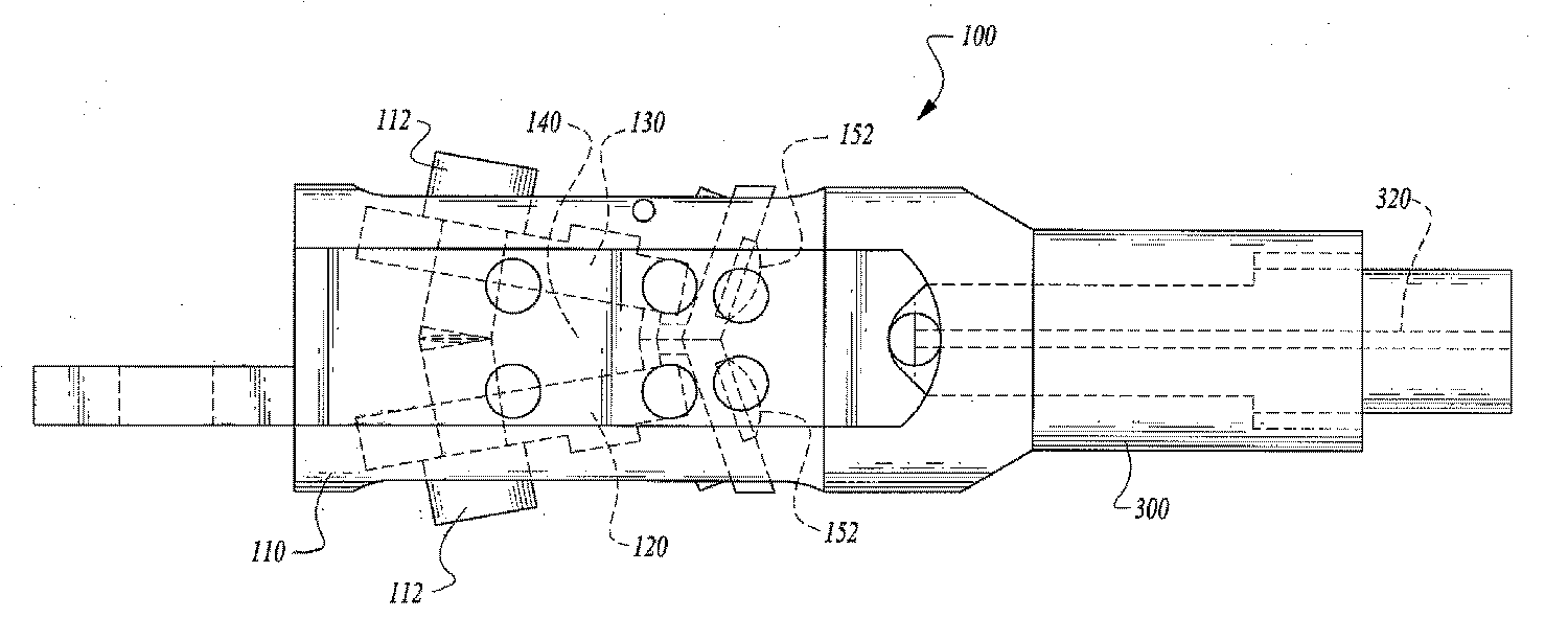
도 1은 베이스 하우징(110), 제어 요소(112), 다이오드 레이저 칩(120 및 130), 레이저 탑재 블록(140), 포커싱 렌즈 블록(150), 비구면 렌즈(152), 및 광섬유 하우징 유닛(300)을 포함하는 듀얼 다이오드 컨버전스 모듈(100)의 실시예에 대한 평면도이다.
도 2는 베이스 하우징(110), 다이오드 레이저 칩(120), 포커싱 렌즈 블록(150), 및 광섬유 하우징 유닛(300)을 묘사하는 듀얼 다이오드 컨버전스 모듈(100)의 실시예에 대한 사시도이다.
도 3은 베이스 하우징(110), 제어 요소(112), 다이오드 레이저 칩(120 및 130), 레이저 탑재 블록(140), 포커싱 렌즈 블록(150), 비구면 렌즈(152), 교정 나사(180), 및 광섬유 하우징 유닛(300)을 포함하는 듀얼 다이오드 컨버전스 모듈(100)의 실시예에 대한 분해 사시도이다.
도 4는 제어 요소(112), 다이오드 레이저 칩(120 및 130), 레이저 탑재 블록(140), 비구면 렌즈(152), 및 광섬유 하우징 유닛(300)을 포함하는 듀얼 다이오드 컨버전스 모듈(100)의 실시예에 대한 상세한 평면도이다.1 shows a
2 is a perspective view of an embodiment of a dual
3 shows the
4 illustrates an implementation of a dual
도 1-4와 관련해 듀얼 다이오드 칩 레이저 컨버전스 모듈(100)이 제시된다.1-4 a dual diode chip
듀얼 다이오드 칩 레이저 컨버전스 모듈(100)은 둘 이상의 다이오드 칩 레이저(120 및 130)를 위한 제어 어셈블리(112)를 보유한 베이스 하우징(110)을 포함하고, 각각의 레이저는 개별적인 파장을 갖는 다이오드 칩 레이저 출력 빔을 방출한다. 하우징(110) 내 다이오드 칩 레이저(120 및 130) 사이에 조립체가 놓여 있는데, 다이오드 레이저 칩들을 이격시키고 각각의 다이오드 칩 레이저 출력 빔을 정렬시키기 위한 것이다.The dual diode chip
하우징(110)은 각각의 다이오드 칩 레이저 출력 빔을 포커싱하기 위한 개별적인 조립체와, 각각의 다이오드 칩 레이저 출력 빔 포커싱 조립체를 교정하기 위한 조립체를 추가로 제공한다. 듀얼 다이오드 칩 레이저 컨버전스 모듈(100)의 실시예가, 1) 둘 이상의 다이오드 칩 레이저의 제어를 위한 제어 요소를 보유한 베이스 하우징(110), 2) 개별적인 파장을 갖는 다이오드 칩 레이저 출력 빔을 각각 방출하는 다이오드 칩 레이저(120 및 130), 3) 다이오드 칩 레이저(120 및 130)를 이격시키고 각각의 다이오드 칩 레이저 출력 빔을 정렬시키기 위한 레이저 탑재 블록(140), 4) 각각의 다이오드 칩 레이저 출력 빔을 위한 비구면 렌즈(152)를 포함하는 포커싱 렌즈 블록(150), 그리고 5) 교정 나사(180)를 포함한다.
듀얼 다이오드 칩 레이저 컨버전스 모듈(100)의 실시예는 800nm의 최적 파장, 길어야 980nm의 파장을 갖는 다이오드 칩 레이저 출력 빔 적외선을 제공한다.An embodiment of the dual diode chip
듀얼 다이오드 칩 레이저 컨버전스 모듈(100)의 실시예에 있어서, 각각의 다이오드 칩 레이저 출력 빔을 포커싱하기 위한 개별적인 조립체가 렌즈 하우징 조립체 내에 내장된 하나 이상의 비구면 렌즈를 포함한다. 렌즈 하우징 조립체(150)는 베이스 하우징(110) 내에 내장된다. 렌즈 하우징 조립체(150)와 이에 포함된 비구면 렌즈(150)가 광섬유 하우징 유닛(300) 내의 광섬유(320)의 말단으로 적외선 에너지를 포커싱한다.In an embodiment of the dual diode chip
듀얼 다이오드 칩 레이저 컨버전스 모듈의 실시예에서, 베이스 하우징(110)은 중심선(142) 및 탑재 블록 중심선(142)에 대하여 동일한 예각 배향을 갖는 둘 이상의 측면(144 및 146)을 갖는 레이저 탑재 블록(140)을 추가로 포함한다. 따라서 탑재 블록이 다이오드 칩 레이저(120 및 130) 사이에 놓여, 다이오드 칩 레이저를 이격시키고 각자의 다이오드 칩 레이저 출력 빔을 광섬유 하우징 유닛(300) 내의 광섬유(320)의 말단의 초점(148)을 향해 정렬시킬 수 있다. 열 싱크(Heat sink) 페이스트를 사용하여 다이오드 칩 레이저(120 및 130) 사이의 열을 소산시킬 수 있다.In an embodiment of the dual diode chip laser convergence module, the
듀얼 다이오드 칩 레이저 컨버전스 모듈(100)의 실시예가, 각각의 다이오드 칩 레이저(120 및 130)를 통해 이어지는 하나 이상의 나사(180)를 사용하여 각각의 다이오드 칩 레이저 출력 빔 포커싱 조립체를 교정하기 위한 조립체와, 광섬유 하우징 유닛(300) 내의 광섬유(320)의 말단의 초점(148)을 향해 각자의 다이오드 칩 레이저 출력 빔을 정렬시키고 다이오드 레이저 칩을 이격시키기 위한 탑재 블록(140)을 포함한다. 각각의 다이오드 칩 레이저 출력 빔 포커싱 조립체를 위한 조립체가, 렌즈 하우징 어셈블리(150) 및 베이스 하우징(100)을 통해 이어지는 하나 이상의 나사(180)를 추가로 포함한다. 각각의 다이오드 칩 레이저 출력 빔 포커싱 수단을 교정하기 위한 조립체가, 레이저 탑재 블록(140) 및 베이스 하우징(100)을 통해 이어지는 하나 이상의 나사(180)를 추가로 포함한다. 전력 측정기(power meter)를 이용하여 장치(100)가 손으로 조정(tuning) 및 교정된다.An embodiment of dual diode chip
듀얼 다이오드 칩 레이저 컨버전스 모듈(110)의 실시예에 있어서, 하나 이상의 마이크로 프로세서가 두 개의 다이오드 칩 레이저(120 및 130)의 출력을 제어한다. In an embodiment of dual diode chip
장치(100)의 실시예에 있어서, 하나 이상의 레이저 칩(120)이 800nm의 파장, 길어야 980nm의 파장을 갖는 최적 출력 적외선을 발생시킨다. In an embodiment of the
장치(100)의 실시예에 있어서, 하나 이상의 레이저 칩(130)이 800nm의 파장, 길어야 980nm의 파장을 갖는 최적 출력 적외선을 발생시킨다. In an embodiment of the
장치(100)의 바람직한 실시예에 있어서, 베이스 하우징(110), 레이저 탑재 블록(140), 및 포커싱 렌즈 블록은 표준 열 싱크 페이스트 방열(dissipation) 물질을 갖는 알루미늄이다.In a preferred embodiment of the
Claims (13)
a) 둘 이상의 다이오드 칩 레이저의 제어를 위한 수단을 보유한 베이스 하우징;
b) 개별적인 파장을 갖는 다이오드 칩 레이저 출력 빔을 각각 방출하는 둘 이상의 다이오드 레이저 칩;
c) 다이오드 레이저 칩들을 이격시키고 각각의 다이오드 칩 레이저 출력 빔을 정렬시키기 위하여 하우징 내에 있으면서 다이오드 레이저 칩들 사이에 놓이는 수단;
d) 각각의 다이오드 칩 레이저 출력 빔을 포커싱하기 위한 개별적인 수단; 그리고
e) 각각의 다이오드 칩 레이저 출력 빔 포커싱 수단을 교정하기 위한 수단
을 포함하는 것을 특징으로 하는 듀얼 다이오드 칩 레이저 컨버전스 모듈.A dual diode chip laser convergence module,
a) a base housing having means for controlling two or more diode chip lasers;
b) two or more diode laser chips each emitting a diode chip laser output beam having a separate wavelength;
c) means placed between the diode laser chips while in the housing to space the diode laser chips and align each diode chip laser output beam;
d) individual means for focusing each diode chip laser output beam; And
e) means for calibrating each diode chip laser output beam focusing means.
Dual diode chip laser convergence module comprising a.
각각의 다이오드 칩 레이저 출력 빔이 800nm 이상의 파장, 길어야 980nm의 파장을 갖는 적외선을 포함하는 것을 특징으로 하는 듀얼 다이오드 칩 레이저 컨버전스 모듈.The method according to claim 1,
A dual diode chip laser convergence module, wherein each diode chip laser output beam comprises an infrared ray having a wavelength of at least 800 nm and a wavelength of at most 980 nm.
각각의 다이오드 칩 레이저 출력 빔을 포커싱하기 위한 개별적인 수단은, 렌즈 하우징을 위한 수단 내에 내장되는 하나 이상의 비구면 렌즈를 포함하고, 여기서 렌즈 하우징을 위한 수단은 베이스 하우징 내에 내장되는 것을 특징으로 하는 듀얼 다이오드 칩 레이저 컨버전스 모듈.The method according to claim 1,
Individual means for focusing each diode chip laser output beam comprises at least one aspherical lens embedded in a means for the lens housing, wherein the means for the lens housing is embedded in the base housing. Laser Convergence Module.
다이오드 레이저 칩들을 이격시키고 각각의 다이오드 칩 레이저 출력 빔을 정렬시키기 위하여 하우징 내에 있으면서 다이오드 레이저 칩들 사이에 놓이는 수단은, 중심선, 및 탑재 블록 중심선에 대하여 예각 배향을 갖는 둘 이상의 측면을 갖는 레이저 탑재 블록을 포함하고, 이로써, 다이오드 레이저 칩들이 블록 중심선을 향해 그리고 출력 빔을 포커싱하기 위한 대응하는 개별적인 수단을 향해 다이오드 칩 레이저 빔을 각각 방출하는 방향으로 둘 이상의 다이오드 레이저 칩들이 탑재 블록 측면에 부착되는 것을 특징으로 하는 듀얼 다이오드 칩 레이저 컨버전스 모듈.The method according to claim 1,
The means placed between the diode laser chips while in the housing to space the diode laser chips and to align each diode chip laser output beam comprises a laser mounting block having a centerline and at least two sides having an acute orientation with respect to the mounting block centerline. Wherein the two or more diode laser chips are attached to the mounting block side in the direction in which the diode laser chips respectively emit the diode chip laser beam towards the block centerline and the corresponding individual means for focusing the output beam. Dual diode chip laser convergence module.
각각의 다이오드 칩 레이저 출력 빔 포커싱 수단을 교정하기 위한 수단은, 각각의 다이오드 칩 레이저, 및 다이오드 레이저 칩들을 이격시키고 각각의 다이오드 칩 레이저 출력 빔을 정렬시키기 위하여 하우징 내에 있으면서 다이오드 레이저 칩들 사이에 놓이는 수단과 연결되는 하나 이상의 나사를 포함하는 것을 특징으로 하는 듀얼 다이오드 칩 레이저 컨버전스 모듈.The method according to claim 1,
Means for calibrating each diode chip laser output beam focusing means include means for placing each diode chip laser and between the diode laser chips while in the housing to space the diode laser chips and align the respective diode chip laser output beams. Dual diode chip laser convergence module comprising one or more screws connected with.
각각의 다이오드 칩 레이저 출력 빔 포커싱 수단을 교정시키기 위한 수단은 렌즈 하우징을 위한 수단 및 베이스 하우징을 통해 이어지는 하나 이상의 나사를 추가로 포함하는 것을 특징으로 하는 듀얼 다이오드 칩 레이저 컨버전스 모듈.The method according to claim 5,
Means for calibrating each diode chip laser output beam focusing means further comprises means for the lens housing and one or more screws leading through the base housing.
각각의 다이오드 칩 레이저 출력 빔 포커싱 수단을 교정하기 위한 수단은 레이저 탑재 블록 및 베이스 하우징을 통해 이어지는 하나 이상의 나사를 추가로 포함하는 것을 특징으로 하는 듀얼 다이오드 칩 레이저 컨버전스 모듈.The method according to claim 4,
Means for calibrating each diode chip laser output beam focusing means further comprises one or more screws leading through the laser mounting block and the base housing.
둘 이상의 다이오드 칩 레이저의 제어를 위한 수단이, 하나 이상의 마이크로 프로세서를 포함하는 것을 특징으로 하는 듀얼 다이오드 칩 레이저 컨버전스 모듈.The method according to claim 1,
Dual diode chip laser convergence module, characterized in that the means for controlling two or more diode chip lasers comprises one or more microprocessors.
둘 이상의 다이오드 레이저 칩들 사이에 열 싱크(heat sink) 페이스트를 추가로 포함하는 것을 특징으로 하는 듀얼 다이오드 칩 레이저 컨버전스 모듈.The method according to claim 1,
And a heat sink paste between the two or more diode laser chips.
하나 이상의 다이오드 칩 레이저 출력 빔이, 800nm의 최적 파장을 갖는 적외선을 포함하는 것을 특징으로 하는 듀얼 다이오드 칩 레이저 컨버전스 모듈.The method according to claim 1,
Wherein the at least one diode chip laser output beam comprises infrared light having an optimal wavelength of 800 nm.
a) 하나 이상의 마이크로 프로세서를 보유한 베이스 하우징;
b) 하나 이상의 마이크로 프로세서에 의해 각각 제어되고, 개별적인 파장을 갖는 다이오드 칩 레이저 출력 빔을 각각 방출하며, 다이오드 레이저 및 인접한 임의의 다이오드 레이저 칩 사이에 열 싱크(heat sink) 페이스트를 갖는 둘 이상의 다이오드 레이저 칩;
c) 중심선, 및 탑재 블록 중심선에 대하여 예각 배향을 갖는 둘 이상의 측면을 가지고 있으며, 이로써 다이오드 레이저 칩들이 블록 중심선 상의 지점을 향해 배향된 다이오드 칩 레이저 출력 빔을 각각 방출하는 방향으로 둘 이상의 다이오드 레이저 칩들이 탑재 블록 측면에 고정되도록 하는, 레이저 탑재 블록;
d) 렌즈 하우징을 위한 수단 내에 내장된 하나 이상의 비구면 렌즈;
e) 각각의 다이오드 칩 레이저 및 레이저 탑재 블록을 통해 이어지는 하나 이상의 나사;
f) 렌즈 하우징을 위한 수단 및 베이스 하우징을 통해 이어지는 하나 이상의 나사
를 포함하는 것을 특징으로 하는 듀얼 다이오드 칩 레이저 컨버전스 모듈.A dual diode chip laser convergence module,
a) a base housing having one or more microprocessors;
b) two or more diode lasers, each controlled by one or more microprocessors, each emitting a diode chip laser output beam having a separate wavelength, and having a heat sink paste between the diode laser and any adjacent diode laser chip; chip;
c) at least two diode laser chips having a centerline and at least two sides having an acute orientation with respect to the mounting block centerline, whereby the diode laser chips respectively emit a diode chip laser output beam oriented towards a point on the block centerline. A laser mounting block, such that they are fixed to the mounting block side;
d) one or more aspherical lenses embedded in means for the lens housing;
e) one or more screws leading through each diode chip laser and laser mounting block;
f) one or more screws leading through the base housing and means for the lens housing;
Dual diode chip laser convergence module comprising a.
각각의 다이오드 칩 레이저 출력 빔이, 800nm 이상의 파장, 길어야 980nm의 파장을 갖는 적외선을 포함하는 것을 특징으로 하는 듀얼 다이오드 칩 레이저 컨버전스 모듈.The method of claim 11,
A dual diode chip laser convergence module, wherein each diode chip laser output beam comprises an infrared ray having a wavelength of at least 800 nm and a wavelength of at most 980 nm.
하나 이상의 다이오드 칩 레이저 출력 빔이, 800nm의 최적 파장을 갖는 적외선을 포함하는 것을 특징으로 하는 듀얼 다이오드 칩 레이저 컨버전스 모듈.
The method of claim 11,
Wherein the at least one diode chip laser output beam comprises infrared light having an optimal wavelength of 800 nm.
Applications Claiming Priority (2)
| Application Number | Priority Date | Filing Date | Title |
|---|---|---|---|
| US12/115,383 | 2008-05-05 | ||
| US12/115,383 US7656923B2 (en) | 2008-05-05 | 2008-05-05 | Dual diode converging module |
Publications (2)
| Publication Number | Publication Date |
|---|---|
| KR20110005729A true KR20110005729A (en) | 2011-01-18 |
| KR101013613B1 KR101013613B1 (en) | 2011-02-10 |
Family
ID=41257045
Family Applications (1)
| Application Number | Title | Priority Date | Filing Date |
|---|---|---|---|
| KR1020107027378A Expired - Fee Related KR101013613B1 (en) | 2008-05-05 | 2009-05-04 | Dual Diode Convergence Module |
Country Status (6)
| Country | Link |
|---|---|
| US (1) | US7656923B2 (en) |
| EP (1) | EP2274805A4 (en) |
| KR (1) | KR101013613B1 (en) |
| AU (1) | AU2009244502B2 (en) |
| CA (1) | CA2721931C (en) |
| WO (1) | WO2009137402A1 (en) |
Families Citing this family (4)
| Publication number | Priority date | Publication date | Assignee | Title |
|---|---|---|---|---|
| US9125677B2 (en) * | 2011-01-22 | 2015-09-08 | Arcuo Medical, Inc. | Diagnostic and feedback control system for efficacy and safety of laser application for tissue reshaping and regeneration |
| WO2014134314A1 (en) * | 2013-03-01 | 2014-09-04 | The Johns Hopkins University | Light sources, medical devices, and methods of illuminating an object of interest |
| JP7043048B2 (en) * | 2017-03-28 | 2022-03-29 | 株式会社Qdレーザ | Laser module and image projection device |
| JP7000105B2 (en) * | 2017-10-04 | 2022-02-04 | シャープ株式会社 | Light emitting device and liquid crystal display device |
Family Cites Families (43)
| Publication number | Priority date | Publication date | Assignee | Title |
|---|---|---|---|---|
| DE2860817D1 (en) * | 1977-07-01 | 1981-10-15 | Post Office | Light source in an optical communications system |
| US5333603A (en) | 1992-02-25 | 1994-08-02 | Daniel Schuman | Endoscope with palm rest |
| US5304172A (en) | 1993-02-11 | 1994-04-19 | Coherent, Inc. | Fiber optic probe |
| US5351330A (en) * | 1993-04-08 | 1994-09-27 | Uniphase Corporation | Laser diode-lens alignment |
| US5616141A (en) | 1993-04-09 | 1997-04-01 | Ion Laser Technology | Laser system for use in dental procedures |
| US5464436A (en) | 1994-04-28 | 1995-11-07 | Lasermedics, Inc. | Method of performing laser therapy |
| US7320594B1 (en) | 1995-08-31 | 2008-01-22 | Biolase Technology, Inc. | Fluid and laser system |
| US6254597B1 (en) | 1995-08-31 | 2001-07-03 | Biolase Technology, Inc. | Tissue remover and method |
| US6231567B1 (en) | 1995-08-31 | 2001-05-15 | Biolase Technology Inc. | Material remover and method |
| JPH1010372A (en) * | 1996-06-20 | 1998-01-16 | Alps Electric Co Ltd | Ld module |
| US6013096A (en) | 1996-11-22 | 2000-01-11 | Tucek; Kevin B. | Hand-held laser light generator device |
| US5927977A (en) | 1996-11-27 | 1999-07-27 | Professional Dental Technologies, Inc. | Dental scaler |
| US6039565A (en) | 1997-01-14 | 2000-03-21 | Chou; Marilyn M. | Combined ultrasonic and laser device and method of use |
| US6099520A (en) | 1997-06-10 | 2000-08-08 | Shimoji; Yutaka | Method of using a cordless medical laser to cure composites and sterilize living tissue |
| US6325791B1 (en) | 1997-06-10 | 2001-12-04 | Yutaka Shimoji | Method of using a cordless medical laser to cure composites |
| US5928220A (en) | 1997-06-10 | 1999-07-27 | Shimoji; Yutaka | Cordless dental and surgical laser |
| US6213998B1 (en) | 1998-04-02 | 2001-04-10 | Vanderbilt University | Laser surgical cutting probe and system |
| JP3188426B2 (en) | 1999-03-12 | 2001-07-16 | ヤーマン株式会社 | Laser irradiation probe |
| US6574401B2 (en) | 1999-03-30 | 2003-06-03 | Ceramoptec Industries, Inc. | Optical fiber-handpiece combination for medical laser treatments |
| US6525310B2 (en) * | 1999-08-05 | 2003-02-25 | Microvision, Inc. | Frequency tunable resonant scanner |
| WO2001010327A1 (en) | 1999-08-11 | 2001-02-15 | Ceramoptec Industries, Inc. | Dental laser scaling device and method |
| US6261310B1 (en) | 1999-10-27 | 2001-07-17 | Ceramoptec Industries, Inc. | Laser safe treatment system |
| KR200225362Y1 (en) | 2000-07-07 | 2001-06-01 | 박종윤 | Portable combined medical laser instrument using high power semiconductor Laser Diode which equipped sensor in front of instrument. |
| US6327942B1 (en) | 2000-08-10 | 2001-12-11 | Lutz File & Tool Company | Multiple bit driver |
| JP2002202442A (en) * | 2000-11-06 | 2002-07-19 | Fuji Photo Film Co Ltd | Coupling laser beam source and aligner |
| US6746473B2 (en) | 2001-03-02 | 2004-06-08 | Erchonia Patent Holdings, Llc | Therapeutic laser device |
| JP3934362B2 (en) * | 2001-05-14 | 2007-06-20 | 大日本スクリーン製造株式会社 | Element support device |
| US7288086B1 (en) | 2001-06-21 | 2007-10-30 | Biolase Technology, Inc. | High-efficiency, side-pumped diode laser system |
| AU2003226326A1 (en) | 2002-04-09 | 2003-10-27 | Altshuler, Gregory | Method and apparatus for processing hard material |
| US6868221B1 (en) | 2002-05-08 | 2005-03-15 | Health Research, Inc. | Fiber optic positioner |
| US20040156743A1 (en) * | 2002-08-28 | 2004-08-12 | Eric Bornstein | Near infrared microbial elimination laser system |
| DE10250912B4 (en) * | 2002-10-31 | 2006-04-27 | Osram Opto Semiconductors Gmbh | coupling device |
| US6916316B2 (en) * | 2002-11-08 | 2005-07-12 | Harvey H. Jay | Hair treatment method |
| USD496101S1 (en) | 2003-01-18 | 2004-09-14 | Owen Mumford Limited | Tip for syringe for taking blood samples |
| JP4361082B2 (en) | 2003-02-25 | 2009-11-11 | トリア ビューティ インコーポレイテッド | Built-in diode laser dermatological treatment device |
| US20040259053A1 (en) | 2003-06-18 | 2004-12-23 | Bekov George I. | Method and apparatus for laser-assisted dental scaling |
| US7088086B2 (en) * | 2003-09-18 | 2006-08-08 | Xytrans, Inc. | Multi-channel radiometer imaging system |
| WO2005044124A1 (en) | 2003-10-30 | 2005-05-19 | Medical Cv, Inc. | Apparatus and method for laser treatment |
| US6992382B2 (en) * | 2003-12-29 | 2006-01-31 | Intel Corporation | Integrated micro channels and manifold/plenum using separate silicon or low-cost polycrystalline silicon |
| US7450858B2 (en) * | 2003-12-31 | 2008-11-11 | Intel Corporation | Apparatus and method for transmitting and receiving wavelength division multiplexing signals |
| AU2005271779B2 (en) | 2004-07-13 | 2009-02-12 | Biolase Technology, Inc. | Fiber tip detector apparatus and related methods |
| JP2006343561A (en) * | 2005-06-09 | 2006-12-21 | Fujitsu Access Ltd | Bidirectional optical communication module |
| US20070023521A1 (en) * | 2005-07-29 | 2007-02-01 | Chester Wildey | Apparatus and method for security tag detection |
-
2008
- 2008-05-05 US US12/115,383 patent/US7656923B2/en active Active
-
2009
- 2009-05-04 KR KR1020107027378A patent/KR101013613B1/en not_active Expired - Fee Related
- 2009-05-04 CA CA2721931A patent/CA2721931C/en active Active
- 2009-05-04 EP EP09743388A patent/EP2274805A4/en not_active Withdrawn
- 2009-05-04 WO PCT/US2009/042707 patent/WO2009137402A1/en not_active Ceased
- 2009-05-04 AU AU2009244502A patent/AU2009244502B2/en not_active Ceased
Also Published As
| Publication number | Publication date |
|---|---|
| CA2721931C (en) | 2016-06-28 |
| KR101013613B1 (en) | 2011-02-10 |
| US7656923B2 (en) | 2010-02-02 |
| CA2721931A1 (en) | 2009-11-12 |
| WO2009137402A8 (en) | 2010-04-15 |
| US20090274179A1 (en) | 2009-11-05 |
| EP2274805A4 (en) | 2011-06-29 |
| WO2009137402A1 (en) | 2009-11-12 |
| AU2009244502A1 (en) | 2009-11-12 |
| AU2009244502B2 (en) | 2011-05-12 |
| EP2274805A1 (en) | 2011-01-19 |
Similar Documents
| Publication | Publication Date | Title |
|---|---|---|
| AU2018271393B2 (en) | High efficiency optical combiner for multiple non-coherent light sources | |
| JP6072213B2 (en) | Full spectrum LED illuminator | |
| CN1993075B (en) | Light source device and endoscope equipped with the same | |
| KR20040005701A (en) | Laser light source for multiplexing laser beam and exposure device | |
| TW200746274A (en) | Laser irradiation device, laser irradiation method, and method for manufacturing modified object | |
| JP3686660B2 (en) | Light irradiation device and optical unit | |
| JP6740766B2 (en) | Optical module | |
| CN102679880A (en) | Confocal measurement device | |
| JP2003158332A (en) | Laser diode array, laser apparatus, synthesized wave laser light source, and light exposure apparatus | |
| KR101013613B1 (en) | Dual Diode Convergence Module | |
| US20220263293A1 (en) | Semiconductor laser and material machining method using a semiconductor laser | |
| US9768583B2 (en) | Multi-channel optical module and manufacture method thereof | |
| JP2021034501A (en) | Light-emitting device | |
| US9548586B2 (en) | Energy integrating device for split semiconductor laser diodes | |
| US20030223685A1 (en) | Optical circuit for condensing laser beams, and light source device | |
| JPWO2017188097A1 (en) | Optical module | |
| JP7071928B2 (en) | Methods and systems for the emission of narrow radiation and the resulting curing | |
| KR101569441B1 (en) | Laser diode module | |
| JP2004361439A (en) | Laser light source device | |
| JP2006108501A (en) | LASER UNIT, OPTICAL ADJUSTMENT METHOD, OPTICAL DEVICE, AND ASSEMBLING METHOD THEREOF | |
| US20120099339A1 (en) | Light engine module and system including same | |
| KR20170049703A (en) | High Power Laser Module |
Legal Events
| Date | Code | Title | Description |
|---|---|---|---|
| PA0105 | International application |
St.27 status event code: A-0-1-A10-A15-nap-PA0105 |
|
| A201 | Request for examination | ||
| A302 | Request for accelerated examination | ||
| E13-X000 | Pre-grant limitation requested |
St.27 status event code: A-2-3-E10-E13-lim-X000 |
|
| N231 | Notification of change of applicant | ||
| P11-X000 | Amendment of application requested |
St.27 status event code: A-2-2-P10-P11-nap-X000 |
|
| P13-X000 | Application amended |
St.27 status event code: A-2-2-P10-P13-nap-X000 |
|
| PA0201 | Request for examination |
St.27 status event code: A-1-2-D10-D11-exm-PA0201 |
|
| PA0302 | Request for accelerated examination |
St.27 status event code: A-1-2-D10-D17-exm-PA0302 St.27 status event code: A-1-2-D10-D16-exm-PA0302 |
|
| PN2301 | Change of applicant |
St.27 status event code: A-3-3-R10-R13-asn-PN2301 St.27 status event code: A-3-3-R10-R11-asn-PN2301 |
|
| PG1501 | Laying open of application |
St.27 status event code: A-1-1-Q10-Q12-nap-PG1501 |
|
| E701 | Decision to grant or registration of patent right | ||
| PE0701 | Decision of registration |
St.27 status event code: A-1-2-D10-D22-exm-PE0701 |
|
| GRNT | Written decision to grant | ||
| PR0701 | Registration of establishment |
St.27 status event code: A-2-4-F10-F11-exm-PR0701 |
|
| PR1002 | Payment of registration fee |
St.27 status event code: A-2-2-U10-U12-oth-PR1002 Fee payment year number: 1 |
|
| PG1601 | Publication of registration |
St.27 status event code: A-4-4-Q10-Q13-nap-PG1601 |
|
| FPAY | Annual fee payment |
Payment date: 20140121 Year of fee payment: 4 |
|
| PR1001 | Payment of annual fee |
St.27 status event code: A-4-4-U10-U11-oth-PR1001 Fee payment year number: 4 |
|
| PN2301 | Change of applicant |
St.27 status event code: A-5-5-R10-R11-asn-PN2301 |
|
| PN2301 | Change of applicant |
St.27 status event code: A-5-5-R10-R14-asn-PN2301 |
|
| FPAY | Annual fee payment |
Payment date: 20150217 Year of fee payment: 5 |
|
| PR1001 | Payment of annual fee |
St.27 status event code: A-4-4-U10-U11-oth-PR1001 Fee payment year number: 5 |
|
| FPAY | Annual fee payment |
Payment date: 20160104 Year of fee payment: 6 |
|
| PR1001 | Payment of annual fee |
St.27 status event code: A-4-4-U10-U11-oth-PR1001 Fee payment year number: 6 |
|
| R18-X000 | Changes to party contact information recorded |
St.27 status event code: A-5-5-R10-R18-oth-X000 |
|
| FPAY | Annual fee payment |
Payment date: 20170102 Year of fee payment: 7 |
|
| PR1001 | Payment of annual fee |
St.27 status event code: A-4-4-U10-U11-oth-PR1001 Fee payment year number: 7 |
|
| LAPS | Lapse due to unpaid annual fee | ||
| PC1903 | Unpaid annual fee |
St.27 status event code: A-4-4-U10-U13-oth-PC1903 Not in force date: 20180201 Payment event data comment text: Termination Category : DEFAULT_OF_REGISTRATION_FEE |
|
| PC1903 | Unpaid annual fee |
St.27 status event code: N-4-6-H10-H13-oth-PC1903 Ip right cessation event data comment text: Termination Category : DEFAULT_OF_REGISTRATION_FEE Not in force date: 20180201 |