KR20100124087A - Memory controller, memory system including the same and method of operating the same - Google Patents
Memory controller, memory system including the same and method of operating the same Download PDFInfo
- Publication number
- KR20100124087A KR20100124087A KR1020090043149A KR20090043149A KR20100124087A KR 20100124087 A KR20100124087 A KR 20100124087A KR 1020090043149 A KR1020090043149 A KR 1020090043149A KR 20090043149 A KR20090043149 A KR 20090043149A KR 20100124087 A KR20100124087 A KR 20100124087A
- Authority
- KR
- South Korea
- Prior art keywords
- data
- state
- received
- randomization
- page
- Prior art date
- Legal status (The legal status is an assumption and is not a legal conclusion. Google has not performed a legal analysis and makes no representation as to the accuracy of the status listed.)
- Ceased
Links
Images


Classifications
-
- G—PHYSICS
- G06—COMPUTING OR CALCULATING; COUNTING
- G06F—ELECTRIC DIGITAL DATA PROCESSING
- G06F12/00—Accessing, addressing or allocating within memory systems or architectures
- G06F12/02—Addressing or allocation; Relocation
- G06F12/0223—User address space allocation, e.g. contiguous or non contiguous base addressing
- G06F12/023—Free address space management
- G06F12/0238—Memory management in non-volatile memory, e.g. resistive RAM or ferroelectric memory
- G06F12/0246—Memory management in non-volatile memory, e.g. resistive RAM or ferroelectric memory in block erasable memory, e.g. flash memory
-
- G—PHYSICS
- G06—COMPUTING OR CALCULATING; COUNTING
- G06F—ELECTRIC DIGITAL DATA PROCESSING
- G06F2212/00—Indexing scheme relating to accessing, addressing or allocation within memory systems or architectures
- G06F2212/10—Providing a specific technical effect
- G06F2212/1032—Reliability improvement, data loss prevention, degraded operation etc
Landscapes
- Engineering & Computer Science (AREA)
- Theoretical Computer Science (AREA)
- Physics & Mathematics (AREA)
- General Engineering & Computer Science (AREA)
- General Physics & Mathematics (AREA)
- Techniques For Improving Reliability Of Storages (AREA)
- Read Only Memory (AREA)
Abstract
본 발명의 실시 예에 따른 메모리 컨트롤러는 데이터를 외부와 교환하도록 구성되는 제 1 인터페이스부, 제 1 인터페이스부를 통해 수신되는 데이터에 기반하여, 수신된 데이터를 임의화(Randomize)할 지 또는 상태 변환할 지의 여부를 판별하는 프로세서, 프로세서의 제어에 응답하여, 제 1 인터페이스를 통해 수신되는 데이터를 임의화하고, 임의화에 기반하여 임의화 정보를 생성하도록 구성되는 임의화부, 프로세서의 제어에 응답하여 제 1 인터페이스를 통해 수신되는 데이터를 상태 변환하고, 상태 변환에 기반하여 변환 정보를 생성하도록 구성되는 상태 변환부, 그리고 임의화부로부터 임의화된 데이터 및 임의화 정보를 수신하고, 변환부로부터 변환된 데이터 및 변환 정보를 수신하고, 그리고 외부와 임의화된 데이터, 임의화 정보, 변환된 데이터, 그리고 변환 정보 중 적어도 하나를 교환하도록 구성되는 제 2 인터페이스부를 포함한다.According to an embodiment of the present disclosure, a memory controller may randomize or state convert received data based on a first interface unit configured to exchange data with an external device, and data received through the first interface unit. A randomization unit configured to randomize data received through the first interface in response to control of the processor and to generate randomization information based on the randomization; 1 A state transformation unit configured to state-transform data received through an interface, and generate transformation information based on the state transformation, and receive randomized data and randomization information from the randomization unit, and convert the data from the transformation unit. And transform information, and external and randomized data, randomization information, transformed data, Hitting comprises a second interface unit configured to exchange at least one of the converted information.
Description
본 발명은 반도체 메모리 장치에 관한 것으로, 더 상세하게는 불휘발성 메모리 장치에 관한 것이다.The present invention relates to a semiconductor memory device, and more particularly to a nonvolatile memory device.
반도체 메모리 장치(semiconductor memory device)는 실리콘 등과 같은 반도체를 이용하여 구현되는 기억장치이다. 반도체 메모리 장치는 크게 휘발성 메모리 장치(Volatile memory device)와 불휘발성 메모리 장치(Nonvolatile memory device)로 구분된다.A semiconductor memory device is a memory device implemented using a semiconductor such as silicon. Semiconductor memory devices are largely classified into volatile memory devices and nonvolatile memory devices.
휘발성 메모리 장치는 전원 공급이 차단되면 저장하고 있던 데이터가 소멸되는 메모리 장치이다. 휘발성 메모리 장치에는 SRAM, DRAM, SDRAM 등이 있다. 불휘발성 메모리 장치는 전원 공급이 차단되어도 저장하고 있던 데이터가 소멸하지 않는 메모리 장치이다. 불휘발성 메모리 장치에는 ROM, PROM, EPROM, EEPROM, 플래시 메모리 장치, PRAM, MRAM, RRAM, FRAM 등이 있다. 플래시 메모리 장치는 크게 노어 타입과 낸드 타입으로 구분된다.Volatile memory devices lose their stored data when their power supplies are interrupted. Volatile memory devices include SRAM, DRAM, SDRAM, and the like. Nonvolatile memory devices are memory devices that do not lose their stored data even when their power supplies are interrupted. Nonvolatile memory devices include ROM, PROM, EPROM, EEPROM, flash memory devices, PRAM, MRAM, RRAM, FRAM, and the like. Flash memory devices are roughly divided into NOR type and NAND type.
본 발명의 목적은 신뢰성이 향상된 사용자 장치(또는 반도체 메모리 장치)를 제공하는 데에 있다.An object of the present invention is to provide a user device (or semiconductor memory device) with improved reliability.
본 발명의 실시 예에 따른 메모리 컨트롤러는 데이터를 외부와 교환하도록 구성되는 제 1 인터페이스부; 상기 제 1 인터페이스부를 통해 수신되는 데이터에 기반하여, 상기 수신된 데이터를 임의화(Randomize)할 지 또는 상태 변환할 지의 여부를 판별하는 프로세서; 상기 프로세서의 제어에 응답하여, 상기 제 1 인터페이스를 통해 수신되는 데이터를 임의화하고, 상기 임의화에 기반하여 임의화 정보를 생성하도록 구성되는 임의화부; 상기 프로세서의 제어에 응답하여 상기 제 1 인터페이스를 통해 수신되는 데이터를 상태 변환하고, 상기 상태 변환에 기반하여 변환 정보를 생성하도록 구성되는 상태 변환부; 그리고 상기 임의화 부로부터 상기 임의화된 데이터 및 상기 임의화 정보를 수신하고, 상기 변환부로부터 상기 변환된 데이터 및 상기 변환 정보를 수신하고, 그리고 외부와 상기 임의화된 데이터, 상기 임의화 정보, 상기 변환된 데이터, 그리고 상기 변환 정보 중 적어도 하나를 교환하도록 구성되는 제 2 인터페이스부를 포함한다.In an embodiment, a memory controller may include a first interface unit configured to exchange data with an external device; A processor that determines whether to randomize or state convert the received data based on the data received through the first interface unit; A randomization unit configured to randomize data received through the first interface and generate randomization information based on the randomization in response to the control of the processor; A state conversion unit configured to state-transform data received through the first interface in response to control of the processor, and generate conversion information based on the state-transformation; And receives the randomized data and the randomization information from the randomization unit, receives the converted data and the conversion information from the conversion unit, and externally and the randomized data, the randomization information, And a second interface configured to exchange at least one of the converted data and the conversion information.
실시 예로서, 상기 제 2 인터페이스를 통해 상기 임의화된 데이터 및 상기 임의화 정보가 수신될 때, 상기 임의화부는 상기 제 2 인터페이스부를 통해 수신되는 상기 임의화 정보를 이용하여 상기 임의화된 데이터를 본래의 데이터로 복원하 도록 구성된다.In exemplary embodiments, when the randomized data and the randomization information are received through the second interface, the randomization unit may select the randomized data using the randomization information received through the second interface unit. It is configured to restore the original data.
실시 예로서, 상기 제 2 인터페이스를 통해 상기 변환된 데이터 및 상기 변환 정보가 전달될 때, 상기 상태 변환부는 상기 제 2 인터페이스부를 통해 수신되는 상기 변환 정보를 이용하여 상기 변환된 데이터를 본래의 데이터로 복원하도록 구성된다.In an embodiment, when the converted data and the conversion information are transmitted through the second interface, the state conversion unit converts the converted data into original data using the conversion information received through the second interface unit. Configured to restore.
실시 예로서, 상기 임의화부는 미리 설정된 시드를 이용하여 랜덤 시퀀스를 발생하고, 상기 랜덤 시퀀스 및 상기 수신된 데이터를 논리 연산하고, 상기 논리 연산의 결과를 상기 임의화된 데이터로서 출력하고, 그리고 상기 시드를 상기 임의화 정보로서 출력하도록 구성된다.In an embodiment, the randomization unit generates a random sequence using a seed set in advance, logically operates the random sequence and the received data, outputs the result of the logical operation as the randomized data, and And output the seed as the randomization information.
실시 예로서, 상기 상태 변환부는 상기 수신된 데이터의 논리 상태들 각각의 수를 카운트하고, 상기 수신된 데이터의 제 1 논리 상태들의 수 및 제 2 논리 상태들의 수를 비교하고, 비교 결과에 따라 상기 제 1 논리 상태들 및 상기 제 2 논리 상태들을 교환하도록 구성된다.In example embodiments, the state converter may count the number of each of the logic states of the received data, compare the number of first logic states and the number of second logic states of the received data, and according to the comparison result. Configured to exchange first logic states and the second logic states.
실시 예로서, 상기 상태 변환부는 상기 수신된 데이터 중 최상위 논리 상태들의 수가 나머지 논리 상태들 각각의 수보다 작아지도록 상기 수신된 데이터를 변환한다.In an embodiment, the state converting unit converts the received data such that the number of most significant logical states of the received data is smaller than the number of each of the remaining logical states.
실시 예로서, 상기 상태 변환부는 상기 수신된 데이터 중 최하위 논리 상태들의 수가 나머지 논리 상태들 각각의 수보다 작아지도록 상기 수신된 데이터를 변환한다.In an embodiment, the state converting unit converts the received data such that the number of lowest logical states among the received data is smaller than the number of each of the remaining logical states.
실시 예로서, 상기 제 1 인터페이스부를 통해 제 1 및 제 2 논리 상태들을 갖는 데이터가 수신될 때, 상기 상태 변환부는 상기 수신된 데이터의 제 1 논리 상태 및 제 2 논리 상태의 수를 카운트하고, 상기 제 1 논리 상태의 수가 상기 제 2 논리 상태의 수보다 작으면 상기 수신된 데이터를 반전하도록 구성된다.In example embodiments, when data having first and second logic states is received through the first interface unit, the state converting unit may count the number of first and second logic states of the received data, and And if the number of first logical states is less than the number of second logical states, invert the received data.
본 발명의 실시 예에 따른 메모리 시스템은 불휘발성 메모리 장치; 그리고 상기 불휘발성 메모리 장치를 제어하도록 구성되는 메모리 컨트롤러를 포함하고, 상기 메모리 컨트롤러는 데이터를 외부와 교환하도록 구성되는 제 1 인터페이스부; 상기 제 1 인터페이스부를 통해 수신되는 데이터에 기반하여, 상기 수신된 데이터를 임의화(Randomize)할 지 또는 상태 변환할 지의 여부를 판별하는 프로세서; 상기 프로세서의 제어에 응답하여, 상기 제 1 인터페이스를 통해 수신되는 데이터를 임의화하고, 상기 임의화에 기반하여 임의화 정보를 생성하도록 구성되는 임의화부; 상기 프로세서의 제어에 응답하여 상기 제 1 인터페이스를 통해 수신되는 데이터를 상태 변환하고, 상기 상태 변환에 기반하여 변환 정보를 생성하도록 구성되는 상태 변환부; 그리고 상기 임의화 부로부터 상기 임의화된 데이터 및 상기 임의화 정보를 수신하고, 상기 변환부로부터 상기 변환된 데이터 및 상기 변환 정보를 수신하고, 그리고 상기 불휘발성 메모리 장치와 데이터를 교환하도록 구성되는 제 2 인터페이스부를 포함한다.In an embodiment, a memory system may include a nonvolatile memory device; And a memory controller configured to control the nonvolatile memory device, wherein the memory controller comprises: a first interface unit configured to exchange data with an external device; A processor that determines whether to randomize or state convert the received data based on the data received through the first interface unit; A randomization unit configured to randomize data received through the first interface and generate randomization information based on the randomization in response to the control of the processor; A state conversion unit configured to state-transform data received through the first interface in response to control of the processor, and generate conversion information based on the state-transformation; And receive the randomized data and the randomization information from the randomization unit, receive the converted data and the conversion information from the conversion unit, and exchange data with the nonvolatile memory device. It includes two interface units.
본 발명의 실시 예에 따른 메모리 컨트롤러의 동작 방법은 외부로부터 데이터를 수신하고; 상기 수신된 데이터에 기반하여 임의화를 수행할 지 또는 상태 변환을 수행할 지 판별하고; 그리고 상기 판별 결과에 따라, 상기 수신된 데이터를 임의화 또는 상태 변환하는 것을 포함한다.According to at least one example embodiment of the inventive concepts, a method of operating a memory controller may include: receiving data from an outside; Determine whether to perform randomization or state transformation based on the received data; And randomizing or state converting the received data according to the determination result.
본 발명에 따르면, 데이터는 임의화 또는 상태 변환되어 저장된다. 따라서, 사용자 장치(또는 반도체 메모리 장치)의 신뢰성이 향상된다.According to the invention, the data is randomized or state converted and stored. Thus, the reliability of the user device (or semiconductor memory device) is improved.
이하에서, 본 발명이 속하는 기술분야에서 통상의 지식을 가진 자가 본 발명의 기술적 사상을 용이하게 실시할 수 있을 정도로 상세히 설명하기 위하여, 본 발명의 실시 예를 첨부된 도면을 참조하여 설명하기로 한다. 동일한 구성 요소들은 동일한 참조 번호를 이용하여 인용될 것이다. 유사한 구성 요소들은 유사한 참조 번호들을 이용하여 인용될 것이다.DETAILED DESCRIPTION Hereinafter, exemplary embodiments of the present invention will be described with reference to the accompanying drawings so that those skilled in the art may easily implement the technical idea of the present invention. . Identical components will be referred to using the same reference numerals. Similar components will be referred to using similar reference numerals.
도 1은 본 발명의 실시 예에 따른 메모리 시스템(10)을 보여주는 블록도이다. 도 1을 참조하면, 본 발명의 실시 예에 따른 메모리 시스템(10)은 컨트롤러(100) 및 불휘발성 메모리 장치(200)를 포함한다.1 is a block diagram illustrating a
컨트롤러(100)는 호스트(Host) 및 불휘발성 메모리 장치(200)에 연결된다. 컨트롤러(100)는 불휘발성 메모리 장치(200)로부터 읽은 데이터를 호스트(Host)에 전달하고, 호스트(Host)로부터 전달되는 데이터를 불휘발성 메모리 장치(200)에 저장하도록 구성된다. 컨트롤러는 도 3을 참조하여 더 상세하게 설명된다.The
불휘발성 메모리 장치(200)는 데이터를 저장하기 위한 메모리 셀 어레이, 메모리 셀 어레이에 데이터를 기입 및 독출하기 위한 읽기 쓰기 회로, 외부로부터 전달되는 어드레스를 디코딩하여 읽기 쓰기 회로에 전달하는 어드레스 디코더, 불휘발성 메모리 장치(200)의 제반 동작을 제어하기 위한 제어 로직 등을 포함할 것이 다. 불휘발성 메모리 장치(200)는 도 2 및 17을 참조하여 더 상세하게 설명된다.The
컨트롤러(100) 및 불휘발성 메모리 장치(200)는 하나의 반도체 장치로 집적될 수 있다. 예시적으로, 컨트롤러(100) 및 불휘발성 메모리 장치(200)는 하나의 반도체 장치로 집적되어, 메모리 카드를 구성할 것이다. 예를 들면, 컨트롤러(100) 및 불휘발성 메모리 장치(200)는 하나의 반도체 장치로 집적되어 PC 카드(PCMCIA), 컴팩트 플래시 카드(CF), 스마트 미디어 카드(SM, SMC), 메모리 스틱, 멀티미디어 카드(MMC, RS-MMC, MMCmicro), SD 카드(SD, miniSD, microSD), 유니버설 플래시 기억장치(UFS) 등을 구성할 것이다.The
다른 예로서, 컨트롤러(100) 및 불휘발성 메모리 장치(200)는 하나의 반도체 장치로 집적되어 반도체 드라이브(SSD, Solid State Drive)를 구성할 것이다. 예시적으로, 반도체 드라이브(SSD)는 반도체 메모리에 데이터를 저장하도록 구성되는 장치를 포함할 것이다. 메모리 시스템(10)이 반도체 드라이브(SSD)로 이용되는 경우, 메모리 시스템(10)에 연결된 호스트(Host)의 동작 속도는 획기적으로 개선될 것이다.As another example, the
다른 예로서, 메모리 시스템(10)은 컴퓨터, 휴대용 컴퓨터, UMPC, 워크스테이션, 넷북(net-book), PDA, 포터블(portable) 컴퓨터, 웹 타블렛(web tablet), 무선 전화기(wireless phone), 모바일 폰(mobile phone), 스마트폰(smart phone), 디지털 카메라(digital camera), 디지털 음성 녹음기(digital audio recorder), 디지털 음성 재생기(digital audio player), 디지털 영상 녹화기(digital picture recorder), 디지털 영상 재생기(digital picture player), 디지털 동영상 녹화 기(digital video recorder), 디지털 동영상 재생기(digital video player), 정보를 무선 환경에서 송수신할 수 있는 장치, 홈 네트워크를 구성하는 다양한 전자 장치들 중 하나, 컴퓨터 네트워크를 구성하는 다양한 전자 장치들 중 하나, 텔레매틱스 네트워크를 구성하는 다양한 전자 장치들 중 하나, 또는 반도체 드라이브(SSD, Solid State Drive) 또는 메모리 카드와 같은 컴퓨팅 시스템을 구성하는 다양한 구성 요소들 중 하나에 적용될 것이다.As another example, the
다른 예로서, 불휘발성 메모리 장치(200) 또는 메모리 시스템(10)은 다양한 형태들의 패키지로 실장 될 수 있다. 예를 들면, 불휘발성 메모리 장치(200) 또는 메모리 시스템(10)은 PoP(Package on Package), Ball grid arrays(BGAs), Chip scale packages(CSPs), Plastic Leaded Chip Carrier(PLCC), Plastic Dual In-Line Package(PDIP), Die in Waffle Pack, Die in Wafer Form, Chip On Board(COB), Ceramic Dual In-Line Package(CERDIP), Plastic Metric Quad Flat Pack(MQFP), Thin Quad Flatpack(TQFP), Small Outline(SOIC), Shrink Small Outline Package(SSOP), Thin Small Outline(TSOP), Thin Quad Flatpack(TQFP), System In Package(SIP), Multi Chip Package(MCP), Wafer-level Fabricated Package(WFP), Wafer-Level Processed Stack Package(WSP) 등과 같은 방식으로 패키지화되어 실장될 것이다.As another example, the
도 2는 도 1의 불휘발성 메모리 장치(200)를 보여주는 블록도이다. 도 2를 참조하면, 본 발명의 실시 예에 따른 불휘발성 메모리 장치(200)는 메모리 셀 어레이(210), 어드레스 디코더(220), 읽기 쓰기 회로(230), 데이터 입출력 회로(240), 그리고 제어 로직(250)을 포함한다.FIG. 2 is a block diagram illustrating the
메모리 셀 어레이(210)는 워드 라인들(WL)을 통해 어드레스 디코더(220)에 연결되고, 비트 라인들(BL)을 통해 읽기 쓰기 회로(230)에 연결된다. 메모리 셀 어레이(210)는 복수의 메모리 셀들을 포함한다. 예시적으로, 행 방향으로 배열되는 메모리 셀들은 워드 라인들(WL)에 연결될 것이다. 열 방향으로 배열되는 메모리 셀들은 비트 라인들(BL)에 연결될 것이다. 예시적으로, 메모리 셀 어레이(210)는 셀 당 하나 또는 그 이상의 비트를 저장할 수 있도록 구성될 것이다.The
어드레스 디코더(220)는 워드 라인들(WL)을 통해 메모리 셀 어레이(210)에 연결된다. 어드레스 디코더(220)는 제어 로직(250)의 제어에 응답하여 동작한다. 어드레스 디코더(220)는 외부로부터 어드레스(ADDR)를 전달받는다. 예시적으로, 어드레스(ADDR)는 도 1의 컨트롤러(100)로부터 전달될 것이다.The
어드레스 디코더(220)는 전달된 어드레스(ADDR) 중 행 어드레스를 디코딩할 것이다. 디코딩된 행 어드레스를 이용하여, 어드레스 디코더(220)는 워드 라인들(WL)을 선택할 것이다. 어드레스 디코더(220)는 전달된 어드레스(ADDR) 중 열 어드레스를 디코딩할 것이다. 디코딩된 열 어드레스는 읽기 쓰기 회로(230)에 전달될 것이다. 예시적으로, 어드레스 디코더(220)는 행 디코더, 열 디코더, 어드레스 버퍼 등과 같이 잘 알려진 구성 요소들을 포함할 것이다.The
읽기 쓰기 회로(230)는 비트 라인들(BL)을 통해 메모리 셀 어레이(210)에 연결되고, 데이터 라인들(DL)을 통해 데이터 입출력 회로(240)에 연결된다. 읽기 쓰기 회로(230)는 제어 로직(250)의 제어에 응답하여 동작한다. 읽기 쓰기 회로(230) 는 어드레스 디코더(220)로부터 디코딩된 열 어드레스를 수신할 것이다. 디코딩된 열 어드레스를 이용하여, 읽기 쓰기 회로(230)는 비트 라인들(BL)을 선택할 것이다.The read /
예시적으로, 읽기 쓰기 회로(230)는 컨트롤러(100)로부터 데이터를 수신하고, 수신된 데이터를 메모리 셀 어레이(210)에 기입할 것이다. 다른 예로서, 읽기 쓰기 회로(230)는 메모리 셀 어레이(210)로부터 데이터를 읽고, 읽어진 데이터를 데이터 입출력 회로(240)에 전달할 것이다. 다른 예로서, 읽기 쓰기 회로(230)는 메모리 셀 어레이(210)의 제 1 저장 영역으로부터 데이터를 읽고, 읽어진 데이터를 메모리 셀 어레이(210)의 제 2 저장 영역에 기입할 것이다. 예를 들면, 읽기 쓰기 회로(230)는 카피-백(copy-back) 동작을 수행할 것이다.In exemplary embodiments, the read /
예시적으로, 읽기 쓰기 회로(230)는 페이지 버퍼, 열 선택 회로 등과 같이 잘 알려진 구성 요소들을 포함할 것이다. 다른 예로서, 읽기 쓰기 회로(230)는 감지 증폭기, 쓰기 드라이버, 열 선택 회로 등과 같이 잘 알려진 구성 요소들을 포함할 것이다.In exemplary embodiments, the read /
데이터 입출력 회로(240)는 데이터 라인들(DL)을 통해 읽기 쓰기 회로(230)에 연결된다. 데이터 입출력 회로(240)는 제어 로직(250)의 제어에 응답하여 동작한다. 데이터 입출력 회로(240)는 외부와 데이터(DATA)를 교환한다. 예시적으로, 데이터 입출력 회로(240)는 도 1의 컨트롤러(100)와 데이터를 교환할 것이다. 외부로부터 전달되는 데이터(DATA)는 데이터 라인들(DL)을 통해 읽기 쓰기 회로(230)에 전달될 것이다. 읽기 쓰기 회로로부터 전달되는 데이터(DATA)는 외부로 출력될 것 이다. 예시적으로, 데이터 입출력 회로(240)는 데이터 버퍼 등과 같이 잘 알려진 구성 요소를 포함할 것이다.The data input /
제어 로직(250)은 어드레스 디코더(220), 읽기 쓰기 회로(230), 그리고 데이터 입출력 회로(240)에 연결된다. 제어 로직(250)은 불휘발성 메모리 장치(200)의 제반 동작을 제어한다. 제어 로직(250)은 외부로부터 전달되는 제어 신호(CTRL)에 응답하여 동작한다. 예시적으로, 제어 신호(CTRL)는 도 1의 컨트롤러(100)로부터 전달될 것이다.The
이하에서, 불휘발성 메모리 장치(200)는 플래시 메모리 장치인 것으로 가정한다. 그러나, 불휘발성 메모리 장치(200)는 플래시 메모리 장치인 것으로 한정되지 않음이 이해될 것이다. 예를 들면, 불휘발성 메모리 장치(200)는 EPROM, EEPROM, 플래시 메모리, PRAM, MRAM, FRAM, RRAM 등의 불휘발성 메모리들로 구성될 수 있음이 이해될 것이다.Hereinafter, it is assumed that the
이하에서, 플래시 메모리 장치(200)는 하나의 메모리 셀에 2 비트를 저장하도록 구성되는 것으로 가정한다. 즉, 플래시 메모리 장치(200)는 하나의 메모리 셀에 최하위 비트(Least Significant Bit) 및 최상위 비트(MSB, Most Significant Bit)를 저장하도록 구성되는 멀티 레벨 셀들을 포함할 것이다. 하나의 메모리 셀은 네 개의 논리 상태들 중 하나로 프로그램될 것이다. 메모리 셀에 프로그램된 논리 상태들은 해당 메모리 셀의 문턱 전압에 의해 구별될 것이다.Hereinafter, it is assumed that the
하나의 워드 라인에 연결된 메모리 셀들은 두 개의 논리적 페이지들을 형성할 것이다. 예시적으로, 하나의 워드 라인에 연결된 메모리 셀들의 최하위 비트들(LSB)은 최하위 페이지를 형성할 것이다. 하나의 워드 라인에 연결된 메모리 셀들의 최상위 비트들(MSB)은 최상위 페이지를 형성할 것이다.Memory cells connected to one word line will form two logical pages. In example embodiments, the least significant bits LSBs of the memory cells connected to one word line may form a least significant page. The most significant bits MSB of the memory cells connected to one word line will form the most significant page.
그러나, 플래시 메모리 장치(200)는 하나의 메모리 셀에 2 비트를 저장하는 것으로 한정되지 않음이 이해될 것이다. 예를 들면, 플래시 메모리 장치(200)는 하나의 메모리 셀에 1 비트를 저장할 수 있음이 이해될 것이다. 다른 예로서, 플래시 메모리 장치(200)는 하나의 메모리 셀에 최하위 비트(LSB), 최상위 비트(MSB), 그리고 적어도 하나의 중간 비트(CSB, Central Significant Bit)를 저장하도록 구성될 수 있음이 이해될 것이다.However, it will be appreciated that the
예시적으로, 플래시 메모리 장치(200)에서 임의 쓰기(random write) 및 임의 읽기(random read)가 지원되는 것으로 가정하자. 임의 쓰기는 플래시 메모리 장치(200)의 페이지보다 작은 용량의 데이터를 플래시 메모리 장치(200)에 기입하는 동작을 나타낼 것이다. 임의 읽기는 플래시 메모리 장치(200)의 페이지보다 작은 용량의 데이터를 플래시 메모리 장치(200)로부터 읽는 동작을 나타낼 것이다.For example, assume that random write and random read are supported in the
도 2에서, 플래시 메모리 장치(200)는 하나의 메모리 셀 어레이(210) 및 하나의 읽기 및 쓰기 회로(230)를 포함하는 것으로 도시되어 있다. 그러나, 플래시 메모리 장치(200)는 복수의 메모리 셀 어레이 및 복수의 읽기 및 쓰기 회로들을 포함할 수 있음이 이해될 것이다. 예시적으로, 플래시 메모리 장치(200)는 독립적으로 읽기 및 쓰기가 가능한 복수의 플레인들을 포함할 것이다.In FIG. 2, the
도 3은 도 1의 컨트롤러(100)를 보여주는 블록도이다. 도 3을 참조하면, 컨트롤러(100)는 시스템 버스(110), 프로세서(120), 램(RAM, Random Access Memory, 130), 오류 정정부(140), 호스트 인터페이스(150), 메모리 인터페이스(160), 그리고 인코딩 및 디코딩부(170)를 포함한다.3 is a block diagram illustrating the
시스템 버스(110)는 컨트롤러(100)의 구성 요소들 사이의 채널을 제공한다. 프로세서(120)는 시스템 버스(110)를 통해 컨트롤러(100)의 구성 요소들을 액세스한다. 프로세서(120)는 컨트롤러(100)의 구성 요소들을 제어할 것이다. 프로세서(120)는 컨트롤러(100)의 제반 동작을 제어할 것이다.
램(130)은 시스템 버스(110)에 연결된다. 예시적으로, 램(130)은 컨트롤러(100)의 동작 메모리로 이용될 것이다. 예를 들면, 프로세서(120)에 의해 구동되는 소프트웨어는 램(130)에 로딩될 것이다. 예를 들면, 컨트롤러(100)의 구성 요소들은 램(130)을 이용하여 미리 설정된 동작을 수행할 것이다. 예시적으로, 램(130)은 버퍼 메모리로 이용될 것이다. 예를 들면, 컨트롤러(100)를 통해 플래시 메모리 장치(200)로 전달되는 데이터는 램(130)에 임시로 저장될 것이다. 플래시 메모리 장치(200)로부터 컨트롤러(100)를 통해 호스트(Host)로 전달되는 데이터는 램(130)에 임시로 저장될 것이다.
오류 정정부(140)는 시스템 버스(110)에 연결된다. 오류 정정부(140)는 플래시 메모리 장치(200)로부터 읽어지는 데이터의 오류를 정정하도록 구성될 것이다. 예를 들면, 오류 정정부(140)는 플래시 메모리 장치(200)에 기입될 사용자 데이터의 오류 체크 데이터를 생성할 것이다. 사용자 데이터 및 오류 체크 데이터는 플래시 메모리 장치(200)에 기입될 것이다. 사용자 데이터 및 오류 체크 데이터가 플래시 메모리 장치(200)로부터 읽어질 때, 오류 정정부(140)는 읽어진 오류 체크 데이 터를 이용하여 사용자 데이터의 오류를 검출 및 정정할 것이다.The
예시적으로, 오류 체크 데이터는 CRC (Cyclic Redundancy Check) 데이터, BCH (Bose, Chaudhuri, and Hocquenghem) 데이터, RS (Reed-Solomon) 데이터 등을 포함할 것이다. 예시적으로, 오류 정정부(140)는 디지털 회로, 아날로그 회로, 또는 디지털 및 아날로그 회로가 결합된 형태의 하드웨어로 구현될 것이다. 다른 예로서, 오류 정정부(140)는 소프트웨어로 구현될 것이다. 다른 예로서, 오류 정정부(140)는 하드웨어 및 소프트웨어가 결합된 형태로 구현될 것이다.For example, the error check data may include Cyclic Redundancy Check (CRC) data, Bose (Chaudhuri, and Hocquenghem) data, Reed-Solomon (RS) data, and the like. In exemplary embodiments, the
호스트 인터페이스(150)는 호스트와 인터페이싱한다. 호스트 인터페이스(150)는 호스트와 통신하기 위한 프로토콜을 포함할 것이다. 예시적으로, 호스트 인터페이스(150)는 USB, MMC, PCI-E, ATA(Advanced Technology Attachment), Serial-ATA, Parallel-ATA, SCSI, ESDI, 그리고 IDE(Integrated Drive Electronics) 등과 같은 다양한 인터페이스 프로토콜들 중 하나를 포함할 것이다.The
메모리 인터페이스(160)는 플래시 메모리 장치(200)와 인터페이싱한다. 메모리 인터페이스(160)는 플래시 메모리 장치(200)와 통신하기 위한 프로토콜을 포함할 것이다. 예를 들면, 메모리 인터페이스(160)는 낸드 프로토콜을 포함할 것이다.The
인코딩 및 디코딩부(170)는 시스템 버스(110)에 연결된다. 인코딩 및 디코딩부(170)는 호스트로부터 호스트 인터페이스(150)를 통해 전달되는 데이터를 인코딩하도록 구성된다. 인코딩된 데이터는 메모리 인터페이스(160)를 통해 플래시 메모리 장치(200)로 전달된다. 인코딩 및 디코딩부(170)는 플래시 메모리 장치(200)로 부터 메모리 인터페이스(160)를 통해 전달되는 데이터를 디코딩하도록 구성된다. 디코딩된 데이터는 호스트 인터페이스(150)를 통해 출력된다.The encoding and
인코딩 및 디코딩부(170)는 임의화부(171) 및 상태 변환부(175)를 포함한다. 임의화부(171)는 호스트 인터페이스(150)를 통해 수신된 데이터를 임의화(이하, 임의화 인코딩이라 칭함)하도록 구성된다. 임의화부(171)는 메모리 인터페이스(160)를 통해 수신되는 데이터를 본래의 데이터로 복원(이하, 임의화 디코딩이라 칭함)하도록 구성된다. 상태 변환부(175)는 호스트 인터페이스(150)를 통해 수신되는 데이터를 상태 변환(이하, 상태 인코딩이라 칭함)하도록 구성된다. 상태 변환부(175)는 메모리 인터페이스(160)를 통해 수신되는 데이터를 본래의 데이터로 복원(이하, 상태 디코딩이라 칭함)하도록 구성된다.The encoding and
예시적으로, 인코딩 및 디코딩부(170)는 디지털 회로, 아날로그 회로, 또는 디지털 및 아날로그 회로가 결합된 구조로 구현될 것이다. 다른 예로서, 인코딩 및 디코딩부(170)는 프로세서(120)에서 구동되는 소프트웨어 형태로 구현될 것이다. 다른 예로서, 인코딩 및 디코딩부(170)는 하드웨어 및 소프트웨어가 결합된 형태로 구현될 것이다.For example, the encoding and
도 4는 도 3의 컨트롤러(100)의 동작을 설명하기 위한 순서도이다. 도 3 및 4를 참조하면, S110 단계에서, 데이터가 수신된다. 예시적으로, 호스트(Host)로부터 호스트 인터페이스(150)를 통해 데이터가 수신될 것이다. 다른 예로서, 플래시 메모리 장치(200)로부터 메모리 인터페이스(160)를 통해 데이터가 수신될 것이다. 예시적으로, 수신되는 데이터는 램(130)에 임시로 저장될 것이다.4 is a flowchart illustrating an operation of the
S120 단계에서, 임의화를 수행할 지의 여부가 판별된다. 예시적으로, 데이터는 호스트(Host)로부터 수신되는 것으로 가정하자. 프로세서(120)는 수신된 데이터에 기반하여, 수신된 데이터를 임의화 인코딩할 지 또는 상태 인코딩할 지의 여부를 판별할 것이다. 예시적으로, 수신된 데이터가 순차 데이터이면, 프로세서(120)는 임의화 인코딩을 수행하는 것으로 판별할 것이다. 순차 데이터는 플래시 메모리 장치(200)의 쓰기 동작의 단위와 같거나 큰 용량의 데이터를 나타낼 것이다.In step S120, it is determined whether to perform randomization. By way of example, assume that data is received from a host. The
플래시 메모리 장치(200)의 쓰기 동작의 단위는 페이지이다. 즉, 수신된 데이터의 용량이 플래시 메모리 장치(200)의 하나의 페이지의 저장 용량과 같거나 크면, 프로세서(120)는 임의화 인코딩을 수행하는 것으로 판별할 것이다. 임의화 인코딩은 미리 설정된 시드(Seed)를 이용하여 수행될 것이다. 임의화 인코딩이 수행되면, 플래시 메모리 장치(200)에 기입된 데이터의 신뢰성이 향상될 것이다.The unit of write operation of the
다른 예로서, 수신된 데이터가 임의 쓰기 데이터이면, 프로세서(120)는 상태 인코딩을 수행하는 것으로 판별할 것이다. 임의 쓰기 데이터는 플래시 메모리 장치(200)의 쓰기 동작의 단위보다 작은 용량의 데이터를 나타낼 것이다. 플래시 메모리 장치(200)의 쓰기 동작의 단위는 페이지이다. 수신된 데이터의 용량이 플래시 메모리 장치(200)의 하나의 페이지의 저장 용량보다 작으면, 프로세서(120)는 상태 인코딩을 수행하는 것으로 판별할 것이다. 상태 인코딩은 수신된 데이터의 논리 상태들을 교환하는 동작을 포함할 것이다. 상태 변환이 수행되면, 플래시 메모리 장치(200)에 기입된 데이터의 신뢰성이 향상될 것이다.As another example, if the received data is random write data, the
다른 예로서, 데이터가 플래시 메모리 장치(200)로부터 수신되면, 인코딩 및 디코딩부(170)는 임의화 디코딩 또는 상태 디코딩을 수행할 것이다. 수신된 데이터가 순차 데이터이면, 임의화부(171)는 임의화 디코딩을 수행할 것이다. 수신된 데이터가 랜덤 데이터이면, 상태 변환부(175)는 상태 디코딩을 수행할 것이다.As another example, when data is received from the
임의화 인코딩 및 디코딩은 도 5를 참조하여 더 상세하게 설명된다. 상태 인코딩 및 디코딩은 도 7 내지 10을 참조하여 더 상세하게 설명된다.Randomization encoding and decoding is described in more detail with reference to FIG. 5. State encoding and decoding is described in more detail with reference to FIGS. 7 to 10.
임의화를 수행하지 않는 것으로 판별되면, S130 단계에서, 수신된 데이터의 상태가 변환될 것이다. 예시적으로, 인코딩 및 디코딩부(170)의 상태 변환부(175)는 수신된 데이터를 상태 인코딩할 것이다. 이후에, S180 단계에서, 변환 정보(CI, Conversion Information)가 생성될 것이다. 변환 정보(CI)는 수신된 데이터의 논리 상태들이 어떻게 교환되어 있는지를 나타내는 정보일 것이다. 변환 정보(CI)는 상태 변환부(175)에서 생성될 것이다.If it is determined that randomization is not performed, in step S130, the state of the received data will be converted. In exemplary embodiments, the
이후에, S190 단계에서, 상태 변환된 데이터 및 변환 정보(CI)가 인코딩된 데이터로서 출력될 것이다. 예를 들면, 상태 변환된 데이터 및 변환 정보(CI)가 메모리 인터페이스(160)를 통해 플래시 메모리 장치(200)로 출력될 것이다. 즉, 상태 변환된 데이터 및 변환 정보(CI)가 플래시 메모리 장치(200)에 기입될 것이다.Thereafter, in step S190, the state converted data and the transformation information CI will be output as encoded data. For example, state converted data and translation information CI may be output to the
S120 단계에서 임의화가 수행되는 것으로 판별되면, S140 단계가 수행될 것이다. S140 단계에서, 수신된 데이터가 임의화 인코딩된다. 예시적으로, 인코딩 및 디코딩부(170)의 임의화부(171)는 수신된 데이터를 임의화 인코딩할 것이다. S150 단계에서, 임의화 정보(RI, Randomization Information)가 생성된다. 임의화 정보(RI)는 수신된 데이터가 어떻게 임의화되었는지를 나타내는 정보일 것이다. 예 를 들면, 임의화 정보(RI)는 임의화 동작 시에 사용된 시드(Seed)를 포함할 것이다. 예시적으로, 임의화 정보(RI)는 임의화부(171)에서 생성될 것이다.If it is determined in step S120 that randomization is performed, step S140 will be performed. In step S140, the received data is randomized encoded. For example, the
S160 단계에서, 스페어 데이터를 상태 변환할 지 판별된다. 예시적으로, 스페어 데이터는 사용자 데이터를 플래시 메모리 장치(200)에서 기입 및 독출하기 위해 요구되는 데이터를 포함할 것이다. 예를 들면, 스페어 데이터는 임의화 동작 시에 사용된 시드(Seed)를 포함할 것이다.In step S160, it is determined whether the state of the spare data is to be converted. In exemplary embodiments, the spare data may include data required for writing and reading the user data in the
시드(Seed)는 임의화 인코딩 및 디코딩을 수행하기 위해 요구되는 데이터이다. 즉, 임의화 인코딩 시에, 사용자 데이터 및 스페어 데이터가 모두 임의화 인코딩되어 플래시 메모리 장치(200)에 저장되는 것으로 가정하자. 읽기 동작 시에, 플래시 메모리 장치(200)로부터 임의화 인코딩된 사용자 데이터 및 스페어 데이터가 읽어질 것이다. 임의화 디코딩을 수행하기 위해, 시드(Seed)가 요구될 것이다. 시드(Seed)는 임의화 인코딩되어 있는 스페어 데이터에 포함되어 있다. 즉, 시드(Seed)가 임의화 인코딩되면, 임의화 디코딩을 수행하는 것이 불가능하다.Seed is data required to perform randomized encoding and decoding. That is, in random encoding, it is assumed that both user data and spare data are randomly encoded and stored in the
시드(Seed)를 포함하는 스페어 데이터가 임의화 인코딩되지 않으면, 스페어 데이터의 신뢰성은 임의화 인코딩된 사용자 데이터보다 낮을 것이다. 스페어 데이터의 신뢰성을 향상하기 위하여, 본 발명의 실시 예에 따른 컨트롤러(100)는 스페어 데이터에 대해 상태 변환을 수행하는 것이 가능하다.If the spare data containing the seed is not randomly encoded, the reliability of the spare data will be lower than the randomly encoded user data. In order to improve the reliability of the spare data, the
스페어 데이터를 상태 변환하는 것으로 판별되면, S170 단계가 수행될 것이다. 스페어 데이터를 상태 변환하지 않는 것으로 판별되면, S190 단계가 수행될 것이다. 스페어 데이터의 상태 변환을 수행할 지의 여부는 플래시 메모리 장치(200) 의 신뢰성, 열화 정도, 프로그램 및 읽기 소요 시간 등을 고려하여 판별될 것이다. 예시적으로, 프로그램/소거 카운트가 미리 설정된 값보다 작으면 스페어 데이터의 상태 변환을 수행하지 않고, 프로그램 소거 카운트가 미리 설정된 값보다 크면 스페어 데이터의 상태 변환을 수행하는 것으로 판별될 수 있을 것이다.If it is determined that the spare data is to be state converted, step S170 will be performed. If it is determined that the spare data is not to be state converted, step S190 will be performed. Whether to perform the state conversion of the spare data will be determined in consideration of the reliability, deterioration degree, program and read time of the
S170 단계에서, 스페어 데이터가 상태 인코딩된다. 상태 변환부(175)는 시드(Seed)를 포함하는 스페어 데이터를 상태 인코딩할 것이다. S170 단계에서 상태 인코딩되는 데이터는 스페어 데이터에 한정되지 않는다. 예시적으로, 상태 인코딩되는 데이터는 임의화 인코딩되지 않은 데이터를 포함할 것이다. S180 단계에서, 변환 정보(CI)가 생성된다. 상태 변환부(175)는 변환 정보(CI)를 생성할 것이다.In step S170, the spare data is state encoded. The
S190 단계에서, 임의화 인코딩된 데이터와 임의화 정보(RI), 그리고 상태 인코딩된 데이터와 변환 정보(CI)가 인코딩된 데이터로서 출력된다. 예시적으로, 인코딩된 데이터는 메모리 인터페이스(160)를 통해 플래시 메모리 장치(200)로 출력될 것이다. 즉, 인코딩된 데이터는 플래시 메모리 장치(200)에 기입될 것이다.In step S190, randomized encoded data and randomization information (RI), and state encoded data and transformation information (CI) are output as encoded data. In exemplary embodiments, the encoded data may be output to the
도 5는 도 3의 임의화부(171)를 보여주는 블록도이다. 도 3 및 5를 참조하면, 임의화부(171)는 시프트 레지스터(172) 및 연산 회로(174)를 포함한다.5 is a block diagram illustrating the
시프트 레지스터(172)는 시드(Seed) 및 클럭(CLK)을 제공받는다. 시프트 레지스터(172)는 시드(Seed)를 저장하도록 구성된다. 시프트 레지스터(172)는 클럭(CLK)에 응답하여 저장되어 있는 시드를 시프트할 것이다.The
예시적으로, 시드(Seed)는 "1011"인 것으로 가정하자. 제 1 클럭이 입력되면, 시프트 레지스터(172)로부터 "1"이 출력될 것이다. 그리고, 시프트 레지 스터(172)는 "1101"을 저장할 것이다. 제 2 클럭이 입력되면, 시프트 레지스터(172)로부터 "1"이 출력될 것이다. 그리고, 시프트 레지스터(172)는 "1110"을 저장할 것이다. 제 3 클럭이 입력되면, 시프트 레지스터(172)로부터 "0"이 출력될 것이다. 그리고, 시프트 레지스터(172)는 "0111"을 저장할 것이다. 제 4 클럭이 입력되면, 시프트 레지스터(172)로부터 "1"이 출력될 것이다. 그리고, 시프트 레지스터(172)는 "1011"을 저장할 것이다.For example, assume that the seed is "1011". When the first clock is input, "1" will be output from the
즉, 시드(Seed)가 4 비트 데이터이면, 제 1 내지 제 4 클럭이 입력되는 동안, 시프트 레지스터(172)에서 시드(Seed)가 순환될 것이다. 그리고, 시드(Seed)가 순환되는 동안, 시드(Seed)가 1 비트 단위로 출력될 것이다. 시프트 레지스터(172)의 출력은 랜덤 시퀀스(RS, Random Sequence)로서 사용될 것이다. 랜덤 시퀀스(RS)는 연산 회로(174)에 전달될 것이다.That is, if the seed is 4-bit data, the seed will be cycled in the
예시적으로, 임의화부(171)에 제공되는 클럭(CLK)은 메모리 인터페이스(160)에 제공되는 클럭과 동기된 클럭일 것이다. 예를 들면, 임의화부(171)에 제공되는 클럭(CLK)은 컨트롤러(100)의 시스템 클럭일 것이다. 다른 예로서, 임의화부(171)에 제공되는 클럭(CLK)은 컨트롤러(100)의 시스템 클럭으로부터 생성되는 내부 클럭일 것이다.In exemplary embodiments, the clock CLK provided to the
연산 회로(174)는 시프트 레지스터(172)로부터 랜덤 시퀀스(RS)를 제공받는다. 연산 회로(174)는 페이지 데이터(PD)를 제공받는다. 예시적으로, 페이지 데이터(PD)는 호스트 인터페이스(150)로부터 제공될 것이다. 즉, 페이지 데이터(PD)는 호스트(Host)로부터 제공되는 쓰기 데이터일 것이다. 다른 예로서, 페이지 데이터(PD)는 메모리 인터페이스(160)로부터 제공될 것이다. 즉, 페이지 데이터(PD)는 불휘발성 메모리 장치(200)로부터 전달되는 읽기 데이터일 것이다.
연산 회로(174)는 페이지 데이터(PD) 및 랜덤 시퀀스(RS)를 논리 연산하도록 구성될 것이다. 예시적으로, 연산 회로(174)는 페이지 데이터(PD) 및 랜덤 시퀀스(RS)의 배타적 논리 합(eXclusive OR)을 출력하도록 구성될 것이다. 예시적으로, 페이지 데이터(PD)가 쓰기 데이터이면, 연산 회로(174)의 출력은 임의화 인코딩된 페이지 데이터(RD)을 것이다. 임의화 인코딩된 페이지 데이터(RD)는 불휘발성 메모리 장치(200)에 저장될 것이다.The
예시적으로, 시드(Seed)는 임의화부(171)에서 유지되는 데이터일 것이다. 예시적으로, 임의화부(171)는 복수의 시드(Seed)를 테이블화하여 저장할 것이다. 수신된 데이터에 기반하여, 복수의 시드(Seed) 중 특정 시드가 선택될 것이다. 예시적으로, 호스트로부터 전달되는 어드레스에 기반하여, 복수의 시드(Seed) 중 특정 시드가 선택될 것이다. 예시적으로, 플래시 메모리 장치(200)의 프로그램 및 소거 횟수에 따라, 복수의 시드(Seed) 중 특정 시드가 선택될 것이다. 다른 예로서, 시드(Seed)는 임의로 생성되는 데이터일 것이다.In exemplary embodiments, the seed may be data maintained by the
다른 예로서, 페이지 데이터(PD)가 읽기 데이터이면, 페이지 데이터(PD)는 임의화 인코딩된 데이터일 것이다. 연산 회로(174)는 페이지 데이터(PD)를 디코딩하여, 본래의 데이터를 출력할 것이다. 예를 들면, 페이지 데이터(PD)가 읽기 데이터이면, 임의화부(171)는 플래시 메모리 장치(200)로부터 페이지 데이터(PD)와 함께 읽어진 스페어 데이터를 이용하여, 페이지 데이터(PD)를 디코딩할 것이다. 임의 화부(171)는 읽어진 스페어 데이터로부터 시드(Seed)를 검출할 것이다.As another example, if the page data PD is read data, the page data PD may be randomly encoded data. The
예를 들면, 읽어진 스페어 데이터는 상태 변환부(175)에서 상태 디코딩될 것이다. 상태 디코딩된 스페어 데이터는 임의화부(171)로 전달될 것이다. 임의화부(171)는 상태 디코딩된 스페어 데이터에서 시드(Seed)를 검출될 것이다. 검출된 시드(Seed)는 시프트 레지스터(172)에 제공될 것이다. 즉, 임의화부(171)는 임의화 인코딩 시에 사용된 시드(Seed)를 이용하여 페이지 데이터(PD)를 임의화 디코딩할 것이다.For example, the read spare data may be state decoded by the
예를 들면, 연산 회로(174)의 출력은 호스트(Host)로 전달될 것이다. 다른 예로서, 연산 회로(174)의 출력은 갱신 및 임의화 인코딩되어 플래시 메모리 장치(200)에 저장될 것이다. 예를 들면, 플래시 메모리 장치(200)로부터 읽어진 데이터는 카피-백(Copy-Back) 될 것이다.For example, the output of
플래시 메모리 장치(200)의 프로그램 동작은 F-N 터널링 또는 열 전자 주입에 의해 수행될 것이다. 플래시 메모리 장치(200)의 프로그램 시에, 전하가 터널 절연막을 통해 전하 저장층에 전달될 것이다. 따라서, 프로그램 동작이 반복될수록, 터널 절연막은 열화될 것이다. 터널 절연막이 열화되면, 해당 메모리 셀의 프로그램 특성이 변화할 것이다.The program operation of the
프로그램된 메모리 셀의 문턱 전압이 높을수록, 해당 메모리 셀의 전하 저장층에 전달되는 전하의 양은 증가할 것이다. 즉, 프로그램된 메모리 셀의 문턱 전압이 높을수록, 해당 메모리 셀이 열화되는 정도는 증가할 것이다. 예시적으로, 제 1 메모리 셀이 제 1 문턱 전압으로 반복적으로 프로그램되고, 제 2 메모리 셀이 제 1 문턱 전압보다 높은 제 2 문턱 전압으로 반복적으로 프로그램되는 것으로 가정하자. 이때, 제 1 및 제 2 메모리 셀들이 열화되는 정도는 상이할 것이다. 예를 들면, 제 2 메모리 셀이 열화된 정도가 제 1 메모리 셀이 열화된 정도보다 클 것이다.The higher the threshold voltage of the programmed memory cell, the greater the amount of charge transferred to the charge storage layer of that memory cell. That is, as the threshold voltage of the programmed memory cell is higher, the degree of degradation of the corresponding memory cell will increase. For example, assume that a first memory cell is repeatedly programmed to a first threshold voltage, and a second memory cell is repeatedly programmed to a second threshold voltage higher than the first threshold voltage. At this time, the degree of degradation of the first and second memory cells will be different. For example, the extent to which the second memory cell is degraded may be greater than the extent to which the first memory cell is degraded.
즉, 메모리 셀들이 동일한 데이터 패턴으로 반복적으로 프로그램되면, 해당 메모리 셀들이 열화되는 정도는 상이할 것이다. 메모리 셀들이 열화되는 정도가 상이하면, 해당 메모리 셀들의 프로그램 특성이 상이할 것이다. 따라서, 해당 메모리 셀들에서 프로그램 오류 또는 읽기 오류가 발생될 확률이 증가할 것이다.That is, if memory cells are repeatedly programmed with the same data pattern, the degree of degradation of the corresponding memory cells will be different. If the degree of degradation of the memory cells is different, the program characteristics of the corresponding memory cells will be different. Therefore, the probability that a program error or a read error occurs in the corresponding memory cells will increase.
임의화부(171)는 페이지 데이터(PD)를 논리 연산하여 임의화된 데이터(RD)를 생성한다. 논리 연산은 선택된 시드(Seed)를 이용하여 수행된다. 즉, 동일한 패턴의 페이지 데이터(PD)가 수신되어도, 임의화 인코딩된 페이지 데이터(RD)의 패턴은 선택된 시드(Seed)에 따라 가변될 것이다. 임의화된 데이터는 플래시 메모리 장치(200)에 기입된다. 따라서, 플래시 메모리 장치(200)에 동일한 패턴의 데이터가 반복적으로 기입되는 것이 방지된다. 즉, 불휘발성 메모리 장치(200)의 신뢰성이 향상된다.The
플래시 메모리 장치(200)의 메모리 셀의 전하 저장층에서, 시간이 경과할수록 전하의 손실(charge loss)이 발생될 것이다. 전하의 손실(charge loss)이 미리 설정된 정도 이상으로 커지면, 해당 메모리 셀에서 읽기 오류가 발생될 것이다. 제 1 문턱 전압을 갖는 제 1 메모리 셀 및 제 1 문턱 전압보다 낮은 제 2 문턱 전압을 갖는 제 2 메모리 셀이 인접하게 위치하는 것으로 가정하자. 제 1 문턱 전압 및 제 2 문턱 전압의 차이가 클수록, 제 1 메모리 셀 및 제 2 메모리 셀 사이의 전기장(electric field)의 세기는 증가할 것이다. 제 1 메모리 셀 및 제 2 메모리 셀 사이의 전기장의 세기가 증가하면, 제 1 메모리 셀에서 전하가 손실되는 정도는 증가할 것이다. 즉, 인접한 제 1 및 제 2 메모리 셀의 문턱 전압들의 차이가 클수록, 제 1 메모리 셀에서 읽기 오류가 발생될 확률이 증가할 것이다.In the charge storage layer of the memory cell of the
인접한 메모리 셀들의 문턱 전압들의 차이가 미리 설정된 값 보다 작아지도록 시드(Seed)가 선택될 수 있음이 이해될 것이다. 이때, 임의화 인코딩된 페이지 데이터(RD)의 신뢰성이 향상될 수 있음이 이해될 것이다.It will be appreciated that the seed can be selected such that the difference in threshold voltages of adjacent memory cells is less than a preset value. At this time, it will be appreciated that the reliability of the randomly encoded page data RD can be improved.
상술한 바와 같이, 수신된 데이터가 순차 데이터일 때, 수신된 데이터는 임의화된다. 따라서, 플래시 메모리 장치(200)에 기입되는 데이터의 신뢰성이 향상될 수 있음이 이해될 것이다.As described above, when the received data is sequential data, the received data is randomized. Therefore, it will be appreciated that the reliability of data written to the
상술한 실시 예에서, 임의화된 데이터의 스페어 데이터는 상태 변환되는 것으로 설명되었다. 그러나, 메모리 시스템(10)의 동작 속도를 향상하기 위하여, 임의화된 데이터의 스페어 데이터를 상태 변환하는 동작은 생략될 수 있음이 이해될 것이다. 이때, 시드(Seed)는 상태 디코딩 없이 스페어 데이터로부터 검출될 것이다.In the above embodiment, spare data of the randomized data has been described as being state transitioned. However, it will be appreciated that in order to speed up the operation of the
도 6은 도 2의 플래시 메모리 장치(200)의 메모리 셀 어레이(210)의 저장 영역을 보여주는 다이어그램이다. 예시적으로, 도 6에 도시된 저장 영역은 페이지(Page)인 것으로 가정한다. 예시적으로, 페이지(Page)의 좌측 영역으로부터 우측 영역으로 진행할수록, 어드레스가 증가하는 것으로 가정한다.FIG. 6 is a diagram illustrating a storage area of the
예시적으로, 도 6의 페이지(Page)에서, 특정 영역(RA)에 대한 읽기 또는 쓰기 동작이 수행되는 것으로 가정한다. 즉, 특정 영역(RA)에 대한 랜덤 읽기 또는 랜덤 쓰기 동작이 수행되는 것으로 가정한다. 특정 영역(RA)은 n 개의 비트들로 구성되고, 저장 영역(RA)의 이전의 어드레스 영역들은 m 개의 비트들로 구성되는 것으로 가정한다.For example, assume that a read or write operation on a specific area RA is performed in the page of FIG. 6. In other words, it is assumed that a random read or a random write operation is performed on a specific area RA. It is assumed that the specific area RA is composed of n bits, and the previous address areas of the storage area RA are composed of m bits.
읽기 및 쓰기 동작 시에, 데이터는 임의화부(171)에서 인코딩 또는 디코딩된다. 도 5를 참조하여 설명된 바와 같이, 임의화 인코딩 및 디코딩은 클럭(CLK)에 응답하여 순차적으로 생성되는 랜덤 시퀀스(RS)를 이용하여 수행된다. 예를 들면, 랜덤 시퀀스(RS)는 어드레스의 카운트 업에 응답하여 순차적으로 생성될 것이다. 따라서, 특정 영역(RA)을 임의화 인코딩 또는 디코딩하기 위하여, m+n 개의 랜덤 시퀀스(RS)가 요구된다. 이중, m 개의 랜덤 시퀀스(RS)는 무시되고, n 개의 랜덤 시퀀스(RS)는 특정 영역(RA)을 임의화 인코딩 또는 디코딩하기 위해 이용될 것이다.In read and write operations, data is encoded or decoded by the
상술한 바와 같이, 랜덤 읽기 및 쓰기 동작 시에, n 개의 비트들로 구성되는 특정 영역(RA)을 액세스하기 위해, m+n 개의 랜덤 시퀀스가 요구된다. m+n 개의 랜덤 시퀀스를 생성하기 위해, m+n 개의 클럭들(CLK)이 요구된다. 따라서, 랜덤 쓰기 및 랜덤 읽기 동작 시에 임의화 동작을 수행하면, 지연 시간이 발생될 것이다. 이와 같은 문제를 해결하기 위하여, 본 발명의 실시 예에 따른 메모리 시스템(10, 도 1 참조)은 랜덤 읽기 및 랜덤 쓰기 시에 상태 인코딩 및 디코딩을 수행한다.As described above, in a random read and write operation, m + n random sequences are required to access a specific area RA consisting of n bits. To generate m + n random sequences, m + n clocks CLK are required. Therefore, if the randomization operation is performed during the random write and random read operations, a delay time will occur. In order to solve such a problem, the memory system 10 (refer to FIG. 1) according to an embodiment of the present invention performs state encoding and decoding at random read and random write.
도 7 내지 10은 도 3의 컨트롤러(100)의 상태 변환 동작을 설명하기 위한 다 이어그램이다. 도 7에서, 가로 축은 논리 상태를 나타내며, 세로 축은 데이터의 수를 나타낸다. 각각의 논리 상태는 2 비트로 구성될 것이다. 데이터가 메모리 셀에 프로그램될 때, 해당 메모리 셀의 문턱 전압은 데이터가 나타내는 논리 상태에 따라 결정될 것이다.7 to 10 are diagrams for describing a state conversion operation of the
도 7에서, 소거 상태(E) 및 제 1 내지 제 3 프로그램 상태(P1~P3)가 도시되어 있다. 예시적으로, 가로 축의 방향을 따라 최하위 내지 최상위 논리 상태들을 나타내는 것으로 가정한다. 예를 들면, 소거 상태(E)는 최하위 논리 상태를 나타내고, 제 3 프로그램 상태(P3)는 최상위 논리 상태는 나타내는 것으로 가정한다.In Fig. 7, the erase state E and the first to third program states P1 to P3 are shown. By way of example, it is assumed to represent the lowest to highest logic states along the direction of the horizontal axis. For example, it is assumed that the erase state E represents the lowest logic state and the third program state P3 represents the highest logic state.
예시적으로, 데이터가 플래시 메모리 장치(200)에 프로그램될 때, 제 1 상태(P1)에 대응하는 문턱 전압은 소거 상태(E)에 대응하는 문턱 전압보다 높고, 제 2 상태(P2)에 대응하는 문턱 전압은 제 1 상태(P1)에 대응하는 문턱 전압보다 높고, 그리고 제 3 상태(P3)에 대응하는 문턱 전압은 제 2 상태(P2)에 대응하는 문턱 전압보다 높은 것으로 가정한다.For example, when data is programmed in the
도 7에 도시된 논리 상태들은 호스트(Host)로부터 전달되는 쓰기 데이터의 논리 상태들을 나타낸다. 도 7을 참조하면, 제 3 프로그램 상태(P3), 소거 상태(E), 제 1 프로그램 상태(P1), 그리고 제 2 프로그램 상태(P2)의 순서로 상태의 수가 많은 것으로 도시되어 있다.Logical states illustrated in FIG. 7 represent logical states of write data transferred from a host. Referring to FIG. 7, the number of states is shown in the order of the third program state P3, the erase state E, the first program state P1, and the second program state P2.
도 7에 도시된 상태들에 대응하는 데이터가 플래시 메모리 장치(200)에 프로그램될 때, 제 3 프로그램 상태(P3)에 대응하는 문턱 전압은 네 개의 논리 상태들(E, P1~P3)에 대응하는 문턱 전압들 중 가장 높다. 따라서, 제 3 프로그램 상태(P3)로 프로그램된 메모리 셀들은 전하 손실(charge loss)의 영향을 가장 강하게 받을 것이다. 또한, 제 3 프로그램 상태(P3)로 프로그램되는 메모리 셀들은 인접한 메모리 셀들에 커플링의 영향을 가장 강하게 전달할 것이다. When data corresponding to the states shown in FIG. 7 are programmed in the
소거 상태(E)에 대응하는 문턱 전압은 네 개의 논리 상태들(E, P1~P3)에 대응하는 문턱 전압들 중 가장 낮다. 따라서, 읽기 동작 시에, 소거 상태(E)로 프로그램된 메모리 셀들은 읽기 전압에 의한 스트레스를 가장 강하게 받을 것이다. 즉, 소거 상태(E)로 프로그램된 메모리 셀들은 읽기 전압 교란의 영향을 가장 강하게 받을 것이다.The threshold voltage corresponding to the erase state E is the lowest among the threshold voltages corresponding to the four logic states E and P1 to P3. Therefore, during the read operation, the memory cells programmed to the erase state E will be most strongly stressed by the read voltage. That is, memory cells programmed to the erase state E will be most strongly affected by the read voltage disturbance.
상태 변환부(175)는 프로그램 데이터 중 제 3 프로그램 상태(P3) 및 소거 상태(E)에 대응하는 데이터의 양이 제 1 및 제 2 프로그램 상태들(P1, P2)에 대응하는 데이터의 양 보다 적어지도록, 프로그램 데이터의 상태를 변환할 것이다.In the
도 8은 플래시 메모리 장치(200)의 프로그램 방법을 보여주는 다이어그램이다. 도 8에서, 가로 축은 전압을 나타내며, 세로 축은 메모리 셀들의 수를 나타낸다. 즉, 도 8은 플래시 메모리 장치(200)의 메모리 셀들의 문턱 전압 산포를 나타낸다.8 is a diagram illustrating a program method of a
플래시 메모리 장치(200)의 프로그램 동작은 두 단계로 구성된다. 우선, 최하위 비트(LSB) 데이터가 수신되면, 최하위 비트(LSB) 프로그램이 수행된다. 최하위 비트(LSB) 프로그램 시에, 메모리 셀들은 소거 상태(E) 또는 프로그램 상태(P)를 갖도록 프로그램된다. 예시적으로, 소거 상태(E)는 "1"을 나타내고, 프로그램 상태(P)는 "0"을 나타내는 것으로 도시되어 있다.The program operation of the
이후에, 최상위 비트(MSB) 데이터가 수신되면, 최상위 비트(MSB) 프로그램이 수행된다. 소거 상태(E)의 메모리 셀들은 소거 상태(E) 또는 제 1 프로그램 상태(P1)로 프로그램될 것이다. 프로그램 상태(P)의 메모리 셀들은 제 2 또는 제 3 프로그램 상태(P2, P3)로 프로그램될 것이다. 예시적으로, 소거 상태(E)는 "11"을 나타내고, 제 1 프로그램 상태(P1)는 "01"을 나타내고, 제 2 프로그램 상태(P2)는 "00"을 나타내고, 그리고 제 3 프로그램 상태(P3)는 "10"을 나타내는 것으로 도시되어 있다.Thereafter, when the most significant bit (MSB) data is received, the most significant bit (MSB) program is performed. The memory cells in the erase state E may be programmed to the erase state E or the first program state P1. The memory cells in the program state P may be programmed to the second or third program states P2 and P3. By way of example, the erase state E represents "11", the first program state P1 represents "01", the second program state P2 represents "00", and the third program state ( P3) is shown to represent "10".
호스트(Host)로부터 LSB 데이터가 수신될 때, 상태 변환부(175)는 상태 인코딩을 수행할 것이다. 예시적으로, 상태 변환부(175)는 수신되는 LSB 데이터의 "0"의 수 및 "1"의 수를 카운트할 것이다. 상태 변환부(175)는 "0"의 수 및 "1"의 수를 비교할 것이다. 비교 결과에 따라, 상태 변환부(175)는 상태 인코딩을 수행할 것이다.When LSB data is received from the host, the
예시적으로, LSB 데이터의 상태 인코딩은 소거 상태(E)로 프로그램되는 메모리 셀들 및 제 3 프로그램 상태(P3)로 프로그램되는 메모리 셀들에 의한 교란에 따라 수행될 것이다.In exemplary embodiments, the state encoding of the LSB data may be performed according to a disturbance caused by the memory cells programmed into the erase state E and the memory cells programmed into the third program state P3.
예를 들면, 소거 상태(E)로 프로그램되는 메모리 셀들에 의한 교란이 제 3 프로그램 상태(P3)로 프로그램되는 메모리 셀들에 의한 교란보다 작은 경우, 상태 변환부(175)는 LSB 데이터의 "1"의 수가 "0"의 수보다 많아지도록 상태 인코딩할 것이다. 즉, LSB 데이터의 "1"의 수가 "0"의 수보다 많으면, 상태 변환부(175)는 LSB 데이터를 유지할 것이다. LSB 데이터의 "1"의 수가 "0"의 수보다 적으면, 상태 변환부(175)는 LSB 데이터를 반전할 것이다.For example, when the disturbance by the memory cells programmed into the erase state E is smaller than the disturbance by the memory cells programmed into the third program state P3, the
다른 예로서, 소거 상태(E)로 프로그램되는 메모리 셀들에 의한 교란이 제 3 프로그램 상태(P3)로 프로그램되는 메모리 셀들에 의한 교란보다 큰 경우, 상태 변환부(175)는 LSB 데이터의 "1"의 수가 "0"의 수보다 적어지도록 상태 인코딩할 것이다. 즉, LSB 데이터의 "1"의 수가 "0"의 수보다 많으면, 상태 변환부(175)는 LSB 데이터를 반전할 것이다. LSB 데이터의 "1"의 수가 "0"의 수보다 적으면, 상태 변환부(175)는 LSB 데이터를 유지할 것이다.As another example, when the disturbance by the memory cells programmed into the erase state E is greater than the disturbance by the memory cells programmed into the third program state P3, the
예시적으로, LSB 데이터의 상태 인코딩 방법은 상태 변환부(175)에서 설정될 것이다. 예를 들면, LSB 데이터의 상태 인코딩 방법은 상태 변환부(175)의 모드 레지스터(미도시)에 저장된 값에 따라 설정될 것이다.In exemplary embodiments, the state encoding method of LSB data may be set by the
예시적으로, 소거 상태(E)로 프로그램되는 메모리 셀들에 의한 교란이 제 3 프로그램 상태(P3)로 프로그램되는 메모리 셀들에 의한 교란보다 작은 것으로 가정한다. 즉, 상태 변환부(175)는 LSB 데이터의 "1"의 수가 "0"의 수보다 많아지도록 상태 인코딩을 수행하는 것으로 가정한다.For example, it is assumed that the disturbance by the memory cells programmed into the erase state E is smaller than the disturbance by the memory cells programmed into the third program state P3. That is, it is assumed that the
도 9는 상태 변환된 최하위 비트(LSB) 데이터를 나타낸다. 도 9에서, 가로축은 논리 상태를 나타내며, 세로 축은 데이터의 수를 나타낸다. 예시적으로, 가로 축의 방향을 따라 최하위 내지 최상위 논리 상태들을 나타내는 것으로 가정한다. 예를 들면, 소거 상태(E)는 최하위 논리 상태를 나타내고, 프로그램 상태(P)는 최상위 논리 상태는 나타내는 것으로 가정한다.9 shows least significant bit (LSB) data that is state transitioned. In Fig. 9, the horizontal axis represents a logic state, and the vertical axis represents the number of data. By way of example, it is assumed to represent the lowest to highest logic states along the direction of the horizontal axis. For example, it is assumed that the erase state E represents the lowest logic state and the program state P represents the highest logic state.
최하위 비트(LSB) 데이터가 수신되면, 상태 변환부(175)는 "1"의 수가 "0"의 수보다 많아지도록 최하위 비트(LSB) 데이터를 변환할 것이다. 예시적으로, "0"의 수가 "1"의 수보다 많으면, 상태 변환부(175)는 최하위 비트(LSB) 데이터를 반전할 것이다. 다른 예로서, "1"의 수가 "0"의 수보다 많으면, 상태 변환부(175)는 LSB 데이터를 유지할 것이다. 즉, LSB 프로그램 시에, 소거 상태(E)의 수가 프로그램 상태(P)의 수보다 많아질 것이다. 도 9에 도시된 데이터가 플래시 메모리 장치(200)에 프로그램될 것이다.When the least significant bit (LSB) data is received, the
MSB 데이터가 수신되면, 상태 변환부(175)는 제 1 프로그램 상태(P1)로 프로그램될 메모리 셀의 수가 소거 상태(E)로 프로그램될 메모리 셀의 수보다 많아지도록, 그리고 제 2 프로그램 상태(P2)로 프로그램될 메모리 셀의 수가 제 3 프로그램 상태(P3)로 프로그램될 메모리 셀의 수보다 많아지도록, MSB 데이터를 상태 인코딩한다.When the MSB data is received, the
예시적으로, 소거 상태(E)의 MSB 데이터는 "1"이고, 제 1 프로그램 상태(P1)의 MSB 데이터는 "0"이고, 제 2 프로그램 상태(P2)의 MSB 데이터는 "0"이고, 그리고 제 3 프로그램 상태(P3)의 MSB 데이터는 "1"인 것으로 도시되어 있다. 즉, 소거 상태(E) 및 제 3 프로그램 상태(P3)의 MSB 데이터는 "0"이며, 제 1 및 제 2 프로그램 상태들(P1, P2)의 MSB 데이터는 "1"이다. 상태 변환부(175)는 MSB 데이터의 "0"의 수가 "1"의 수보다 많아지도록 MSB 데이터를 상태 인코딩한다.For example, the MSB data of the erase state E is "1", the MSB data of the first program state P1 is "0", the MSB data of the second program state P2 is "0", And the MSB data of the third program state P3 is shown to be "1". That is, the MSB data of the erase state E and the third program state P3 are "0", and the MSB data of the first and second program states P1 and P2 are "1". The
예를 들면, MSB 데이터의 "0"의 수가 "1"의 수보다 많으면, 상태 변환부(171)는 MSB 데이터를 유지할 것이다. MSB 데이터의 "0"의 수가 "1"의 수보다 많으면, 상태 변환부(171)는 MSB 데이터를 반전할 것이다.For example, if the number of " 0 " of the MSB data is larger than the number of " 1 ", the
도 10은 상태 변환된 최상위 비트(MSB) 데이터를 나타낸다. 도 16에서, 가로축은 논리 상태를 나타내며, 세로 축은 데이터의 수를 나타낸다. 예시적으로, 가로 축의 방향을 따라 최하위 내지 최상위 논리 상태들을 나타내는 것으로 가정한다. 예를 들면, 소거 상태(E)는 최하위 논리 상태를 나타내고, 제 3 프로그램 상태(P3)는 최상위 논리 상태는 나타내는 것으로 가정한다.10 shows state shifted most significant bit (MSB) data. In Fig. 16, the horizontal axis represents a logic state, and the vertical axis represents the number of data. By way of example, it is assumed to represent the lowest to highest logic states along the direction of the horizontal axis. For example, it is assumed that the erase state E represents the lowest logic state and the third program state P3 represents the highest logic state.
최상위 비트(MSB) 데이터가 수신되면, 상태 변환부(175)는 "0"의 수가 "1"의 수보다 많아지도록 최상위 비트 데이터(MSB)를 변환할 것이다. 예시적으로, "1"의 수가 "0"의 수보다 많으면, 상태 변환부(175)는 최상위 비트(MSB) 데이터를 반전할 것이다.When the most significant bit (MSB) data is received, the
최하위 비트(LSB)의 "1"로부터 프로그램되는 메모리 셀들은 "11" 또는 "01"로 프로그램될 것이다. 최상위 비트(MSB) 프로그램이 수행되면, "01"의 수가 "11"의 수보다 많을 것이다. 즉, 상태 변환이 수행되면, 제 1 프로그램 상태(P1)의 수가 소거 상태(E)의 수보다 항상 많을 것이다. 따라서, 소거 상태(E)로 프로그램되는 메모리 셀들로 인한 교란이 감소될 것이다.Memory cells programmed from "1" of the least significant bit (LSB) will be programmed to "11" or "01". If the most significant bit (MSB) program is executed, the number of "01" will be more than the number of "11". That is, if state transition is performed, the number of first program states P1 will always be greater than the number of erase states E. FIG. Therefore, the disturbance due to the memory cells programmed into the erase state E will be reduced.
최하위 비트(LSB)의 "0"으로부터 프로그램되는 메모리 셀들은 "00" 또는 "10"으로 프로그램될 것이다. 최상위 비트(MSB) 프로그램이 수행되면, "00"의 수가 "10"의 수보다 많을 것이다. 즉, 상태 변환이 수행되면, 제 3 프로그램 상태(P3)의 수가 제 2 프로그램 상태(P2)의 수보다 항상 많을 것이다. 따라서, 제 3 프로그램 상태(P3)로 프로그램되는 메모리 셀들로 인한 교란이 감소될 것이다.Memory cells programmed from "0" of the least significant bit (LSB) will be programmed to "00" or "10". If the most significant bit (MSB) program is executed, the number of "00" will be more than the number of "10". That is, if state transition is performed, the number of third program states P3 will always be greater than the number of second program states P2. Therefore, the disturbance due to the memory cells programmed into the third program state P3 will be reduced.
상태 인코딩이 수행되면, 상태 변환부(175)는 변환 정보(CI)를 생성할 것이 다. 예시적으로, 변환 정보(CI)는 대응하는 LSB 데이터가 반전되었는지, 그리고 대응하는 MSB 데이터가 반전되었는지를 나타낼 것이다. 플래시 메모리 장치(200)로부터 상태 인코딩된 데이터가 읽어질 때, 변환 정보(CI)가 함께 읽어질 것이다. 상태 변환부(175)는 변환 정보(CI)를 이용하여, 읽어진 데이터를 상태 디코딩할 것이다.When state encoding is performed, the
랜덤 쓰기 동작 시에, 플래시 메모리 장치(200)의 저장 영역(RA, 도 6 참조)에 기입될 데이터가 수신되는 것으로 가정한다. 상태 변환부(175)는 수신된 데이터를 상태 디코딩하고, 변환 정보(CI)를 생성할 것이다. 상태 디코딩된 데이터는 저장 영역(RA)에 기입되고, 변환 정보(CI)는 저장 영역(RA)에 대응하는 스페어 영역에 기입될 것이다.In the random write operation, it is assumed that data to be written in the storage area RA (see FIG. 6) of the
랜덤 읽기 동작 시에, 플래시 메모리 장치(200)의 저장 영역(RA)으로부터 데이터가 수신되는 것으로 가정한다. 이때, 저장 영역(RA)에 대응하는 스페어 영역으로부터, 저장 영역(RA)에 저장된 데이터에 대응하는 변환 정보(CI)가 함께 읽어질 것이다. 상태 변환부(175)는 수신된 변환 정보(CI)를 이용하여 수신된 데이터를 상태 디코딩할 것이다.In the random read operation, it is assumed that data is received from the storage area RA of the
예시적으로, 저장 영역(RA)은 섹터일 것이다. 그리고, 변환 정보(CI)를 저장하기 위한 스페어 영역은 섹터 단위로 제공될 것이다. 즉, 메모리 시스템(10)에서, 섹터 단위로 랜덤 읽기 및 쓰기를 수행하는 것이 가능함이 이해될 것이다. 그러나, 메모리 시스템(10)의 랜덤 읽기 및 쓰기의 단위는 섹터로 한정되지 않음이 이해될 것이다.In exemplary embodiments, the storage area RA may be a sector. A spare area for storing the conversion information CI will be provided in sector units. That is, it will be understood that in the
도 11 내지 13은 도 3의 컨트롤러(100)의 상태 변환 동작의 다른 실시 예를 설명하기 위한 다이어그램이다. 도 11 내지 13에서, 가로 축은 논리 상태를 나타내며, 세로 축은 데이터의 수를 나타낸다. 각각의 논리 상태는 2 비트로 구성될 것이다. 데이터가 메모리 셀에 프로그램될 때, 해당 메모리 셀의 문턱 전압은 데이터가 나타내는 논리 상태에 따라 결정될 것이다.11 to 13 are diagrams for describing another example of the state transition operation of the
예시적으로, 호스트(Host)로부터 수신되는 데이터는 도 8에 도시된 바와 같은 상태들을 갖는 것으로 가정한다. 상태 변환부(175)는 소거 상태(E) 및 제 1 내지 제 3 프로그램 상태들(E, P1~P3)의 수를 각각 카운트할 것이다.For example, it is assumed that data received from a host has states as shown in FIG. 8. The
상태 변환부(175)는 제 3 프로그램 상태(P3)의 수가 적어지도록, 데이터가 나타내는 상태들을 변환할 것이다. 예시적으로, 상태 변환부(175)는 제 1 내지 제 3 상태들(P1~P3) 중 제 3 프로그램 상태(P3)의 수가 가장 적어지도록, 데이터가 나타내는 상태들을 변환할 것이다. 도 7에서, 제 1 내지 제 3 프로그램 상태들(P1~P3) 중 제 2 프로그램 상태(P2)의 수가 가장 적은 것으로 도시되어 있다. 상태 변환부(175)는 제 2 프로그램 상태(P2) 및 제 3 프로그램 상태(P3)를 교환할 것이다. 즉, 제 3 프로그램 상태(P3)를 나타내는 데이터는 제 2 프로그램 상태(P2)를 나타내는 것으로 변환될 것이다. 그리고, 제 2 프로그램 상태(P2)를 나타내는 데이터는 제 3 프로그램 상태(P3)를 나타내는 것으로 변환될 것이다. 상태 변환된 결과는 도 11에 도시되어 있다.The
도 11을 참조하면, 도 7의 상태들과 비교하여 제 3 프로그램 상태(P3)의 수가 감소되어 있다. 따라서, 제 3 프로그램 상태(P3)로 프로그램되는 메모리 셀들에 의한 커플링 및 전하 손실이 감소될 것이다.Referring to FIG. 11, the number of third program states P3 is reduced compared to the states of FIG. 7. Thus, coupling and charge loss by the memory cells programmed into the third program state P3 will be reduced.
다른 예로서, 상태 변환부(175)는 소거 상태(E)와 제 1 및 제 2 프로그램 상태들(P1, P2) 중 소거 상태(E)의 수가 가장 적어지도록, 데이터의 상태들을 변환할 것이다. 도 7에서, 소거 상태(E)와 제 1 및 제 2 프로그램 상태들(P1, P2) 중 제 2 프로그램 상태(P2)의 수가 가장 적은 것으로 도시되어 있다. 상태 변환부(175)는 소거 상태(E) 및 제 2 프로그램 상태(P2)를 교환할 것이다. 즉, 소거 상태(E)를 나타내는 데이터는 제 2 프로그램 상태(P2)를 나타내는 것으로 변환될 것이다. 그리고, 제 2 프로그램 상태(P2)를 나타내는 데이터는 소거 상태(E)를 나타내는 것으로 변환될 것이다. 상태 변환된 결과는 도 12에 도시되어 있다.As another example, the
도 12를 참조하면, 도 7의 상태들과 비교하여 소거 상태(E)의 수가 감소되어 있다. 따라서, 소거 상태(E)로 프로그램되는 메모리 셀들에 의한 읽기 전압 교란이 감소될 것이다.Referring to FIG. 12, the number of erase states E is reduced compared to the states of FIG. 7. Thus, the read voltage disturbance by the memory cells programmed into the erase state E will be reduced.
다른 예로서, 상태 변환부(175)는 소거 상태(E) 및 제 3 프로그램 상태(P3)의 수가 제 1 및 제 2 상태들(P1, P2)의 수보다 적어지도록, 수신된 데이터의 상태들을 변환할 것이다. 예시적으로, 상태 변환부(175)는 제 3 프로그램 상태(P3)의 수가 가장 적어지도록, 그리고 소거 상태(E)의 수가 두 번째로 작아지도록, 데이터의 상태들을 변환할 것이다. 예를 들면, 상태 변환부(175)는 제 2 프로그램 상태(P2)와 제 3 프로그램 상태(P3)를 교환하고, 그리고 소거 상태(E)와 제 1 프로그램 상태(P1)를 교환할 것이다.As another example, the
즉, 제 3 프로그램 상태(P3)를 나타내는 데이터는 제 2 프로그램 상태(P2)를 나타내는 것으로 변환될 것이다. 그리고, 제 2 프로그램 상태(P2)를 나타내는 데이 터는 제 3 프로그램 상태(P3)를 나타내는 것으로 변환될 것이다. 소거 상태(E)를 나타내는 데이터는 제 1 프로그램 상태(P1)를 나타내는 것으로 변환될 것이다. 그리고, 제 1 프로그램 상태(P1)를 나타내는 데이터는 소거 상태(E)를 나타내는 것으로 변환될 것이다. 상태 변환된 결과는 도 13에 도시되어 있다.In other words, the data representing the third program state P3 will be converted to represent the second program state P2. Then, the data representing the second program state P2 will be converted to represent the third program state P3. The data representing the erased state E will be converted to represent the first program state P1. Then, the data representing the first program state P1 will be converted into that representing the erase state E. FIG. The result of the state transition is shown in FIG.
도 13을 참조하면, 도 7의 상태들과 비교하여 제 3 프로그램 상태(P3) 및 소거 상태(E)의 수가 감소되어 있다. 따라서, 제 3 프로그램 상태(P3) 및 소거 상태(E)로 프로그램되는 메모리 셀들에 의한 교란들이 감소될 것이다.Referring to FIG. 13, the number of the third program state P3 and the erase state E is reduced compared to the states of FIG. 7. Thus, disturbances by the memory cells programmed to the third program state P3 and the erase state E will be reduced.
커플링, 전하 손실, 읽기 전압 교란 등과 같은 영향을 고려하여, 소거 상태(E)의 수가 가장 작고 그리고 제 3 프로그램 상태(P3)의 수가 두 번째로 작아지도록 변환될 수 있음이 이해될 것이다. 또한, 커플링, 전하 손실, 읽기 전압 교란 등과 같은 영향을 고려하여, 제 1 및 제 2 프로그램 상태들(P1, P2) 또한 변환될 수 있음이 이해될 것이다.It will be appreciated that taking into account effects such as coupling, charge loss, read voltage disturbances, etc., the number of erase states E can be converted to the smallest and the second number of third program states P3 to be made second. Further, it will be appreciated that the first and second program states P1 and P2 can also be converted, taking into account effects such as coupling, charge loss, read voltage disturbances and the like.
상태 변환부(175)는 상태 인코딩 결과에 기반하여 변환 정보(CI)를 생성할 것이다. 변환 정보(CI)는 상태 인코딩에 대한 정보를 포함할 것이다. 읽기 동작 시에, 플래시 메모리 장치(200)로부터 읽기 데이터 및 변환 정보(CI)가 읽어질 것이다. 상태 변환부(175)는 읽어진 변환 정보(CI)를 이용하여 읽기 데이터를 상태 디코딩할 것이다.The
상술한 바와 같이, 순차 데이터는 임의화되고, 랜덤 쓰기 데이터는 상태 변환된다. 따라서, 불휘발성 메모리 장치(200)에 저장되는 데이터의 신뢰성이 향상된다.As described above, the sequential data is randomized, and the random write data is state converted. Therefore, the reliability of data stored in the
상술한 바와 같이, 순차 데이터는 임의화되고, 순차 데이터의 스페어 데이터는 상태 변환된다. 따라서, 사용자 데이터 뿐 아니라 스페어 데이터의 신뢰성 또한 향상된다.As described above, the sequential data is randomized, and the spare data of the sequential data is state converted. Therefore, reliability of spare data as well as user data is improved.
상술한 실시 예에서, 랜덤 읽기 및 쓰기 동작 시에 상태 변환이 수행되는 것으로 설명되었다. 그러나, 순차 읽기 및 쓰기 동작 시에도 상태 변환이 수행될 수 있음이 이해될 것이다.In the above-described embodiment, it has been described that the state transition is performed during the random read and write operations. However, it will be appreciated that state transitions may also be performed during sequential read and write operations.
도 14는 도 2의 플래시 메모리(200)의 다른 실시 예를 보여주는 블록도이다. 도 14를 참조하면, 플래시 메모리 장치(200)는 제 1 및 제 2 플레인들(200a, 200b)을 포함한다. 제 1 및 제 2 플레인들(200a, 200b)은 독립적으로 읽기 및 쓰기가 가능할 것이다. 도 11에서, 제 1 및 제 2 플레인들(200a, 200b)에 대응하는 읽기 및 쓰기 회로들, 어드레스 디코더들, 데이터 입출력 회로들, 그리고 제어 로직들은 생략되어 있다.14 is a block diagram illustrating another embodiment of the
제 1 플레인(200a)에서 제 1 페이지(Page1)가 도시되어 있고, 제 2 플레인(200b)에서 제 2 페이지(Page2)가 도시되어 있다. 예시적으로, 플래시 메모리 장치(200)는 복수 플레인 프로그램 기능을 지원하는 것으로 가정한다. 복수 플레인 프로그램은 복수의 플레인들에 대해 동시에 프로그램 동작을 수행하는 기능을 나타낸다.A first page Page1 is shown in the
예시적으로, 플래시 메모리 장치(200)에서, 복수 플레인 프로그램 시에 제 1 페이지(Page1) 및 제 2 페이지(Page2)가 동시에 프로그램될 것이다. 예를 들면, 제 1 페이지(Page1)에 프로그램될 데이터가 플래시 메모리 장치(200)에 로딩되고, 제 2 페이지(Page2)에 프로그램될 데이터가 플래시 메모리 장치(200)에 로딩될 것이다. 이후에, 제 1 및 제 2 페이지들(Page1, Page2)에서 동시에 프로그램 동작이 수행될 것이다. 따라서, 제 1 및 제 2 페이지들(Page1, Page2)의 프로그램 시간이 단축된다.For example, in the
예시적으로, 제 1 및 제 2 페이지들(Page1, Page2)은 물리적 페이지들을 나타내는 것으로 가정하자. 즉, 제 1 페이지(Page1)는 최하위 페이지 및 최상위 페이지들을 포함할 것이다. 또한, 제 2 페이지(Page2)는 최하위 페이지 및 최상위 페이지들을 포함할 것이다.For example, assume that the first and second pages Page1 and Page2 represent physical pages. That is, the first page Page1 may include the lowest page and the highest page. In addition, the second page Page2 may include the lowest page and the highest page.
도 15는 복수 플레인 프로그램 및 상태 변환 동작 시에 플래시 메모리(200)에 데이터를 로딩하는 제 1 실시 예를 보여주는 블록도이다. 도 14 및 15를 참조하면, 제 1 페이지 데이터(PD1)는 제 1 페이지(Page1)의 최하위 페이지에 기입될 데이터를 나타낸다. 제 2 페이지 데이터(PD2)는 제 2 페이지(Page2)의 최하위 페이지에 기입될 데이터를 나타낸다. 제 3 페이지 데이터(PD3)는 제 1 페이지(Page2)의 최상위 페이지에 기입될 데이터를 나타낸다. 제 4 페이지 데이터(PD4)는 제 2 페이지(Page2)의 최상위 페이지에 기입될 데이터를 나타낸다. 그리고 제 1 페이지 데이터(PD1)로부터 제 4 페이지 데이터(PD4)의 순서로 데이터가 수신되는 것으로 가정한다.FIG. 15 is a block diagram illustrating a first embodiment of loading data into a
도 11 내지 13을 참조하여 설명된 바와 같이, 상태 변환을 수행하기 위해 4 개의 논리 상태들의 수가 요구된다. 즉, 하나의 물리 페이지의 프로그램을 위해, 최하위 페이지 데이터 및 최상위 페이지 데이터가 모두 요구된다.As described with reference to FIGS. 11-13, four logical states are required to perform state transitions. That is, for the program of one physical page, both the lowest page data and the highest page data are required.
컨트롤러(200)는 제 1 페이지 데이터(PD1)를 제 1 페이지(Page1)의 최하위 페이지 데이터로, 그리고 제 2 페이지 데이터(PD2)를 제 1 페이지(Page1)의 최상위 페이지 데이터로 할당한다. 그리고, 제 3 페이지 데이터(PD3)를 제 2 페이지(Page2)의 최하위 페이지 데이터로, 그리고 제 4 페이지 데이터(PD4)를 제 2 페이지의 최상위 페이지 데이터로 할당한다.The
제 1 페이지 데이터(PD1)의 첫 번째 비트 및 제 2 페이지 데이터(PD2)의 첫 번째 비트는 제 1 페이지(Page1)의 첫 번쩨 메모리 셀에 기입될 논리 상태를 나타낼 것이다. 마찬가지로, 제 1 페이지 데이터(PD1)의 k 번째 비트 및 제 2 페이지 데이터(PD2)의 k 번째 비트는 제 1 페이지(Page1)의 k 번째 메모리 셀에 기입될 논리 상태를 나타낼 것이다. 따라서, 제 2 페이지 데이터(PD2)가 입력되기 시작하면, 제 1 페이지(Page1)를 위한 상태 변환 동작(예를 들면, 논리 상태들의 수의 카운팅)을 시작하는 것이 가능하다.The first bit of the first page data PD1 and the first bit of the second page data PD2 will indicate a logic state to be written to the first memory cell of the first page Page1. Similarly, the k th bit of the first page data PD1 and the k th bit of the second page data PD2 will indicate a logical state to be written to the k th memory cell of the first page Page1. Therefore, when the second page data PD2 starts to be input, it is possible to start a state transition operation (for example, counting the number of logical states) for the first page Page1.
제 1 및 제 2 페이지 데이터(PD1, PD2)는 상태 인코딩되어 변환된 제 1 및 제 2 페이지 데이터(TPD1, TPD2)를 형성할 것이다. 변환된 제 1 페이지 데이터(TPD1)는 제 1 페이지(Page1)의 최하위 페이지에 기입되기 위해 플래시 메모리 장치(200)로 전송될 것이다. 변환된 제 2 페이지 데이터(TPD2)는 제 1 페이지(Page1)의 최상위 페이지에 기입되기 위해 플래시 메모리 장치(200)로 전송될 것이다.The first and second page data PD1 and PD2 will be state encoded to form the converted first and second page data TPD1 and TPD2. The converted first page data TPD1 may be transmitted to the
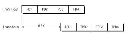
변환된 제 1 및 제 2 페이지 데이터(TPD1, TPD2)가 플래시 메모리 장치(200)로 전송되는 동안, 제 3 및 제 4 페이지 데이터(PD3, PD4)의 수신과 상태 변환이 수행될 것이다. 제 3 및 제 4 페이지 데이터(PD3, PD4)는 상태 인코딩되어 변환된 제 3 및 제 4 페이지 데이터(TPD3, TPD4)를 형성할 것이다. 변환된 제 1 및 제 2 페이지 데이터(TPD1, TPD2)의 전송이 완료되면, 변환된 제 3 및 제 4 페이지 데이터(TPD3, TPD4)가 제 2 페이지(Page2)의 최하위 및 최상위 페이지에 기입되기 위해 플래시 메모리 장치(200)에 전송될 것이다.While the converted first and second page data TPD1 and TPD2 are transmitted to the
제 1 페이지 데이터(PD1)가 입력된 후, 변환된 제 1 페이지 데이터(TPD1)가 출력될 때까지, 제 1 시간(△T1) 만큼의 지연이 발생될 것이다. 그러나, 상술한 바와 같이, 제 2 페이지 데이터(PD2)가 수신되면 변환된 제 1 및 제 2 페이지 데이터(TPD1, TPD2)를 생성하는 것이 가능하다. 변환된 제 1 및 제 2 페이지 데이터(TPD1, TPD2)가 출력되는 동안, 제 3 및 제 4 페이지 데이터(PD3, PD4)가 수신된다. 제 3 및 제 4 페이지 데이터(PD3, PD4)가 수신되면, 변환된 제 3 및 제 4 페이지 데이터(TPD3, TPD4)를 생성하는 것이 가능하다. 변환된 제 2 페이지 데이터(TPD2)의 출력이 완료되면, 변환된 제 3 페이지 데이터(TPD3)이 지연 없이 출력될 수 있다. 즉, 페이지 데이터(PD1~PD4)의 수신 및 변환된 페이지 데이터(TPD1~TPD4)의 출력은 파이프 라인 방식으로 수행된다. 따라서, 초기의 제 1 시간(△T1)의 지연 외에, 상태 변환 동작 시에 발생되는 지연은 존재하지 않는다.After the first page data PD1 is input, a delay by the first time DELTA T1 will occur until the converted first page data TPD1 is output. However, as described above, when the second page data PD2 is received, it is possible to generate the converted first and second page data TPD1 and TPD2. While the converted first and second page data TPD1 and TPD2 are output, the third and fourth page data PD3 and PD4 are received. When the third and fourth page data PD3 and PD4 are received, it is possible to generate the converted third and fourth page data TPD3 and TPD4. When the output of the converted second page data TPD2 is completed, the converted third page data TPD3 may be output without delay. That is, the reception of the page data PD1 to PD4 and the output of the converted page data TPD1 to TPD4 are performed in a pipelined manner. Therefore, in addition to the delay of the initial first time DELTA T1, no delay occurs during the state transition operation.
도 16은 복수 플레인 프로그램 및 상태 변환 동작 시에 플래시 메모리(200)에 데이터를 로딩하는 제 2 실시 예를 보여주는 블록도이다. 도 14 및 16을 참조하면, 제 1 페이지 데이터(PD1)는 제 1 페이지(Page1)의 최하위 페이지에 기입될 데이터를 나타낸다. 제 2 페이지 데이터(PD2)는 제 2 페이지(Page1)의 최하위 페이지 에 기입될 데이터를 나타낸다. 제 3 페이지 데이터(PD3)는 제 1 페이지(Page2)의 최상위 페이지에 기입될 데이터를 나타낸다. 제 4 페이지 데이터(PD4)는 제 2 페이지(Page2)의 최상위 페이지에 기입될 데이터를 나타낸다. 그리고 제 1 페이지 데이터(PD1)로부터 제 4 페이지 데이터(PD4)의 순서로 데이터가 수신되는 것으로 가정한다.FIG. 16 is a block diagram illustrating a second embodiment of loading data into a
도 11 내지 13을 참조하여 설명된 바와 같이, 상태 변환을 수행하기 위해 4 개의 논리 상태들의 수가 요구된다. 즉, 하나의 물리 페이지의 프로그램을 위해, 최하위 페이지 데이터 및 최상위 페이지 데이터가 모두 요구된다.As described with reference to FIGS. 11-13, four logical states are required to perform state transitions. That is, for the program of one physical page, both the lowest page data and the highest page data are required.
컨트롤러(200)는 제 1 페이지 데이터(PD1)를 제 1 페이지(Page1)의 최하위 페이지 데이터로, 그리고 제 2 페이지 데이터(PD2)를 제 2 페이지(Page2)의 최하위 페이지 데이터로 할당한다. 그리고, 제 3 페이지 데이터(PD3)를 제 1 페이지(Page1)의 최상위 페이지 데이터로, 그리고 제 4 페이지 데이터(PD4)를 제 2 페이지의 최상위 페이지 데이터로 할당한다.The
제 1 페이지 데이터(PD1)의 첫 번째 비트 및 제 3 페이지 데이터(PD3)의 첫 번째 비트는 제 1 페이지(Page1)의 첫 번째 메모리 셀에 기입될 논리 상태를 나타낼 것이다. 마찬가지로, 제 1 페이지 데이터(PD1)의 k 번째 비트 및 제 3 페이지 데이터(PD2)의 k 번째 비트는 제 1 페이지(Page1)의 k 번째 메모리 셀에 기입될 논리 상태를 나타낼 것이다. 따라서, 제 3 페이지 데이터(PD3)가 입력되기 시작하면, 제 1 페이지(Page1)를 위한 상태 변환 동작(예를 들면, 논리 상태들의 수의 카운팅)을 시작하는 것이 가능하다. 마찬가지로, 제 4 페이지 데이터(PD4)가 입력 되기 시작하면, 제 2 페이지(Page2)를 위한 상태 변환 동작(예를 들면, 논리 상태들의 수의 카운팅)을 시작하는 것이 가능하다.The first bit of the first page data PD1 and the first bit of the third page data PD3 may indicate a logic state to be written to the first memory cell of the first page Page1. Similarly, the k th bit of the first page data PD1 and the k th bit of the third page data PD2 will indicate a logic state to be written to the k th memory cell of the first page Page1. Therefore, when the third page data PD3 starts to be input, it is possible to start a state transition operation (for example, counting the number of logical states) for the first page Page1. Similarly, when the fourth page data PD4 starts to be input, it is possible to start a state transition operation (e.g., counting the number of logical states) for the second page Page2.
제 1 및 제 3 페이지 데이터(PD1, PD3)는 상태 인코딩되어 변환된 제 1 및 제 2 페이지 데이터(TPD1, TPD2)를 형성할 것이다. 변환된 제 1 페이지 데이터(TPD1)는 제 1 페이지(Page1)의 최하위 페이지에 기입되기 위해 플래시 메모리 장치(200)로 전송될 것이다. 변환된 제 2 페이지 데이터(TPD2)는 제 1 페이지(Page1)의 최상위 페이지에 기입되기 위해 플래시 메모리 장치(200)로 전송될 것이다.The first and third page data PD1 and PD3 will be state encoded to form the converted first and second page data TPD1 and TPD2. The converted first page data TPD1 may be transmitted to the
변환된 제 1 및 제 2 페이지 데이터(TPD1, TPD2)가 플래시 메모리 장치(200)로 전송되는 동안, 제 4 페이지 데이터(PD4)의 수신과 제 2 및 제 4 페이지 데이터(PD2, PD4)의 상태 변환이 수행될 것이다. 제 2 및 제 4 페이지 데이터(PD2, PD4)는 상태 인코딩되어 변환된 제 3 및 제 4 페이지 데이터(TPD3, TPD4)를 형성할 것이다. 변환된 제 1 및 제 2 페이지 데이터(TPD1, TPD2)의 전송이 완료되면, 변환된 제 3 및 제 4 페이지 데이터(TPD3, TPD4)가 제 2 페이지(Page2)의 최하위 및 최상위 페이지에 기입되기 위해 플래시 메모리 장치(200)에 전송될 것이다.While the converted first and second page data TPD1 and TPD2 are transmitted to the
제 1 페이지 데이터(PD1)가 입력된 후, 변환된 제 1 페이지 데이터(TPD1)가 출력될 때까지, 제 2 시간(△T2) 만큼의 지연이 발생될 것이다. 그러나, 상술한 바와 같이, 제 3 페이지 데이터(PD3)가 수신되면 변환된 제 1 및 제 2 페이지 데이터(TPD1, TPD2)를 생성하는 것이 가능하다. 변환된 제 1 및 제 2 페이지 데이터(TPD1, TPD2)가 출력되는 동안, 제 4 페이지 데이터(PD4)가 수신된다. 제 4 페이 지 데이터(PD4)가 수신되면, 변환된 제 3 및 제 4 페이지 데이터(TPD3, TPD4)를 생성하는 것이 가능하다. 변환된 제 2 페이지 데이터(TPD2)의 출력이 완료되면, 변환된 제 3 페이지 데이터(TPD3)가 지연 없이 출력될 수 있다. 즉, 페이지 데이터(PD1~PD4)의 수신 및 변환된 페이지 데이터(TPD1~TPD4)의 출력은 파이프 라인 방식으로 수행된다. 따라서, 초기의 제 2 시간(△T2)의 지연 외에, 상태 변환 동작 시에 발생되는 지연은 존재하지 않는다.After the first page data PD1 is input, a delay by the second time DELTA T2 will occur until the converted first page data TPD1 is output. However, as described above, when the third page data PD3 is received, it is possible to generate the converted first and second page data TPD1 and TPD2. While the converted first and second page data TPD1 and TPD2 are output, the fourth page data PD4 is received. When the fourth page data PD4 is received, it is possible to generate the converted third and fourth page data TPD3 and TPD4. When the output of the converted second page data TPD2 is completed, the converted third page data TPD3 may be output without delay. That is, the reception of the page data PD1 to PD4 and the output of the converted page data TPD1 to TPD4 are performed in a pipelined manner. Therefore, in addition to the delay of the initial second time DELTA T2, no delay occurs during the state transition operation.
도 15 및 16을 참조하여 설명된 로딩 방법은 임의화 인코딩 시에도 적용될 수 있음이 이해될 것이다. 예시적으로, 제 2 페이지 데이터(PD2)가 수신되기 시작할 때, 제 1 및 제 2 페이지 데이터(PD1, PD2)가 임의화 인코딩될 것이다. 예를 들면, 제 1 페이지 데이터(PD1) 및 제 2 페이지 데이터(PD2)가 도 5의 연산 회로(174)에 제공될 것이다. 제 1 및 제 2 페이지 데이터(PD1, PD2)는 임의화 인코딩되어 변환된 제 1 및 제 2 페이지 데이터(TPD1, TPD2)를 형성할 것이다.It will be appreciated that the loading method described with reference to FIGS. 15 and 16 can also be applied at random encoding. By way of example, when the second page data PD2 starts to be received, the first and second page data PD1 and PD2 will be randomly encoded. For example, the first page data PD1 and the second page data PD2 may be provided to the
다른 예로서, 제 3 페이지 데이터(PD3)가 수신되기 시작할 때, 제 1 및 제 3 페이지 데이터(PD1, PD3)가 임의화 인코딩될 것이다. 예를 들면, 제 1 페이지 데이터(PD1) 및 제 3 페이지 데이터(PD3)가 도 5의 연산 회로(174)에 제공될 것이다. 제 1 및 제 3 페이지 데이터(PD1, PD3)는 임의화 인코딩되어 변환된 제 1 및 제 2 페이지 데이터(TPD1, TPD2)를 형성할 것이다.As another example, when the third page data PD3 starts to be received, the first and third page data PD1 and PD3 will be randomly encoded. For example, the first page data PD1 and the third page data PD3 may be provided to the
도 17은 도 1의 플래시 메모리 장치(200)의 다른 실시 예(300)를 보여주는 블록도이다. 도 17을 참조하면, 플래시 메모리 장치(300)는 메모리 셀 어레이(310), 어드레스 디코더(320), 읽기 및 쓰기 회로(330), 데이터 입출력 회로(340), 제어 로직(350), 그리고 인코딩 및 디코딩부(360)를 포함한다.17 is a block diagram illustrating another
메모리 셀 어레이(310), 어드레스 디코더(320), 읽기 및 쓰기 회로(330), 데이터 입출력 회로(340), 제어 로직(350)은 도 2를 참조하여 설명된 메모리 셀 어레이(210), 어드레스 디코더(220), 읽기 및 쓰기 회로(230), 데이터 입출력 회로(240), 제어 로직(250)과 마찬가지로 동작할 것이다. 따라서, 상세한 설명은 생략된다.The
도 2를 참조하여 설명된 플래시 메모리 장치(200)와 비교하면, 플래시 메모리 장치(300)는 인코딩 및 디코딩부(360)를 더 포함한다. 즉, 인코딩 및 디코딩 동작은 컨트롤러(100)가 아닌 플래시 메모리 장치(300)에서 수행되도록 구성된다. 인코딩 및 디코딩부(360)는 임의화부(361) 및 상태 변환부(365)를 포함한다. 임의화부(361)는 도 3 내지 5를 참조하여 설명된 바와 마찬가지로 임의화 인코딩 및 디코딩을 수행하도록 구성될 것이다. 상태 변환부(365)는 도 3, 4, 6 내지 16을 참조하여 설명된 바와 마찬가지로 동작할 것이다. 따라서, 상세한 설명은 생략된다.Compared with the
도 18은 도 1의 메모리 시스템(10)을 포함하는 컴퓨팅 시스템(400)을 보여주는 블록도이다. 도 18을 참조하면, 본 발명의 실시 예에 따른 컴퓨팅 시스템(400)은 중앙 처리 장치(410), 램(420, RAM, Random Access Memory), 사용자 인터페이스(430), 전원(440), 그리고 메모리 시스템(10)을 포함한다.18 is a block diagram illustrating a
메모리 시스템(10)은 시스템 버스(450)를 통해, 중앙처리장치(410), 램(420), 사용자 인터페이스(430), 그리고 전원(440)에 전기적으로 연결된다. 사용자 인터페이스(430)를 통해 제공되거나, 중앙 처리 장치(410)에 의해서 처리된 데 이터는 메모리 시스템(10)에 저장된다. 메모리 시스템(10)은 컨트롤러(100) 및 불휘발성 메모리 장치(200, 300)를 포함한다.The
메모리 시스템(10)이 반도체 드라이브(SSD)로 장착되는 경우, 컴퓨팅 시스템(300)의 부팅 속도가 획기적으로 빨라질 수 있다. 도면에 도시되지 않았지만, 본 발명에 따른 시스템은 응용 칩셋(Application Chipset), 카메라 이미지 프로세서(Camera Image Processor) 등을 더 포함할 수 있음은 이 분야의 통상적인 지식을 습득한 자들에게 이해될 것이다.When the
본 발명의 상세한 설명에서는 구체적인 실시 예에 관하여 설명하였으나, 본 발명의 범위와 기술적 사상에서 벗어나지 않는 한도 내에서 여러 가지 변형이 가능함은 자명하다. 그러므로 본 발명의 범위는 상술한 실시 예에 국한되어 정해져서는 안되며 후술하는 특허청구범위뿐만 아니라 이 발명의 특허청구범위와 균등한 것들에 의해 정해져야 한다.In the detailed description of the present invention, specific embodiments have been described, but it is obvious that various modifications can be made without departing from the scope and spirit of the present invention. Therefore, the scope of the present invention should not be limited to the above-described embodiments, but should be determined by the claims equivalent to the claims of the present invention as well as the claims of the following.
도 1은 본 발명의 실시 예에 따른 메모리 시스템을 보여주는 블록도이다.1 is a block diagram illustrating a memory system according to an example embodiment of the disclosure.
도 2는 도 1의 불휘발성 메모리 장치를 보여주는 블록도이다.FIG. 2 is a block diagram illustrating a nonvolatile memory device of FIG. 1.
도 3은 도 1의 컨트롤러를 보여주는 블록도이다.3 is a block diagram illustrating the controller of FIG. 1.
도 4는 도 3의 컨트롤러의 동작을 설명하기 위한 순서도이다.4 is a flowchart for describing an operation of the controller of FIG. 3.
도 5는 도 3의 임의화부를 보여주는 블록도이다.5 is a block diagram illustrating the randomization unit of FIG. 3.
도 6은 도 2의 불휘발성 메모리 장치의 메모리 셀 어레이의 저장 영역을 보여주는 다이어그램이다.6 is a diagram illustrating a storage area of a memory cell array of the nonvolatile memory device of FIG. 2.
도 7 내지 10은 도 3의 컨트롤러의 상태 변환 동작을 설명하기 위한 다이어그램이다.7 to 10 are diagrams for describing a state transition operation of the controller of FIG. 3.
도 11 내지 13은 도 3의 컨트롤러의 상태 변환 동작의 다른 실시 예를 설명하기 위한 다이어그램이다.11 to 13 are diagrams for describing another example of a state transition operation of the controller of FIG. 3.
도 14은 도 2의 플래시 메모리의 다른 실시 예를 보여주는 블록도이다.14 is a block diagram illustrating another embodiment of the flash memory of FIG. 2.
도 15는 복수 플레인 프로그램 및 상태 변환 동작 시에 플래시 메모리에 데이터를 로딩하는 제 1 실시 예를 보여주는 블록도이다.FIG. 15 is a block diagram illustrating a first embodiment of loading data into a flash memory during a multi-plane program and state transition operation.
도 16은 복수 플레인 프로그램 및 상태 변환 동작 시에 플래시 메모리에 데이터를 로딩하는 제 2 실시 예를 보여주는 블록도이다.16 is a block diagram illustrating a second embodiment of loading data into a flash memory during a multi-plane program and state transition operation.
도 17은 도 1의 플래시 메모리 장치 다른 실시 예를 보여주는 블록도이다.17 is a block diagram illustrating another embodiment of the flash memory device of FIG. 1.
도 18은 도 1의 메모리 시스템을 포함하는 컴퓨팅 시스템을 보여주는 블록도이다.18 is a block diagram illustrating a computing system including the memory system of FIG. 1.
Claims (10)
Priority Applications (3)
| Application Number | Priority Date | Filing Date | Title |
|---|---|---|---|
| KR1020090043149A KR20100124087A (en) | 2009-05-18 | 2009-05-18 | Memory controller, memory system including the same and method of operating the same |
| US12/777,676 US8549328B2 (en) | 2009-05-18 | 2010-05-11 | Memory controller, memory system including the same, and method for operating the same |
| US14/041,404 US20140032824A1 (en) | 2009-05-18 | 2013-09-30 | Memory Controller, Memory System Including the Same, and Method for Operating the Same |
Applications Claiming Priority (1)
| Application Number | Priority Date | Filing Date | Title |
|---|---|---|---|
| KR1020090043149A KR20100124087A (en) | 2009-05-18 | 2009-05-18 | Memory controller, memory system including the same and method of operating the same |
Publications (1)
| Publication Number | Publication Date |
|---|---|
| KR20100124087A true KR20100124087A (en) | 2010-11-26 |
Family
ID=43069467
Family Applications (1)
| Application Number | Title | Priority Date | Filing Date |
|---|---|---|---|
| KR1020090043149A Ceased KR20100124087A (en) | 2009-05-18 | 2009-05-18 | Memory controller, memory system including the same and method of operating the same |
Country Status (2)
| Country | Link |
|---|---|
| US (2) | US8549328B2 (en) |
| KR (1) | KR20100124087A (en) |
Cited By (3)
| Publication number | Priority date | Publication date | Assignee | Title |
|---|---|---|---|---|
| US9965205B2 (en) | 2014-12-18 | 2018-05-08 | SK Hynix Inc. | Data storage device performing a scramble operation and operating method thereof |
| KR20200137542A (en) * | 2019-05-30 | 2020-12-09 | 에스케이하이닉스 주식회사 | Memory controller and storage device having the same |
| KR20210094696A (en) * | 2020-01-21 | 2021-07-30 | 삼성전자주식회사 | Non-volatile memory device, storage device and program method thereof |
Families Citing this family (14)
| Publication number | Priority date | Publication date | Assignee | Title |
|---|---|---|---|---|
| US7961520B2 (en) | 2009-08-18 | 2011-06-14 | Seagate Technology Llc | Encoding and decoding to reduce switching of flash memory transistors |
| KR20130080203A (en) * | 2012-01-04 | 2013-07-12 | 삼성전자주식회사 | Program data generating method in view of asymmetric characteristic of cell states and memory system using the same |
| US10236045B2 (en) * | 2012-09-21 | 2019-03-19 | Samsung Electronics Co., Ltd. | Semiconductor memory device having detection clock patterns phase-inverted from each other and detection clock generating method thereof |
| KR20140076127A (en) * | 2012-12-12 | 2014-06-20 | 에스케이하이닉스 주식회사 | Non-Volatile Memory Apparatus and Operating Method Thereof, and Data Processing System Having the Same |
| KR20140100330A (en) * | 2013-02-06 | 2014-08-14 | 삼성전자주식회사 | Memory system and operating method thereof |
| KR102244617B1 (en) | 2014-03-13 | 2021-04-26 | 삼성전자 주식회사 | Device and method for processing data using logical information and physical information |
| US9727261B2 (en) * | 2015-09-24 | 2017-08-08 | Western Digital Technologies, Inc. | Weighted programming patterns in solid-state data storage systems |
| CN111679787B (en) * | 2016-04-27 | 2023-07-18 | 慧荣科技股份有限公司 | Flash memory device, flash memory controller, and flash memory storage management method |
| US10019314B2 (en) | 2016-04-27 | 2018-07-10 | Silicon Motion Inc. | Flash memory apparatus and storage management method for flash memory |
| KR20190033791A (en) * | 2017-09-22 | 2019-04-01 | 에스케이하이닉스 주식회사 | Controller, semiconductor memory device and memory system having the same |
| CN108845844A (en) * | 2018-05-30 | 2018-11-20 | 郑州云海信息技术有限公司 | A kind of state transition method and device |
| KR102669450B1 (en) * | 2018-12-11 | 2024-05-28 | 에스케이하이닉스 주식회사 | Storage device and operating method thereof |
| KR102847329B1 (en) | 2019-08-01 | 2025-08-14 | 삼성전자주식회사 | A memory device, a memory controller and a memory system including the same for performing state shaping operation |
| US12211385B2 (en) | 2021-09-30 | 2025-01-28 | Volkswagen Group of America Investments, LLC | Distributed method and system for vehicle identification tracking |
Family Cites Families (13)
| Publication number | Priority date | Publication date | Assignee | Title |
|---|---|---|---|---|
| US6917542B2 (en) * | 2003-07-29 | 2005-07-12 | Sandisk Corporation | Detecting over programmed memory |
| US8552891B2 (en) * | 2006-05-27 | 2013-10-08 | Samsung Electronics Co., Ltd. | Method and apparatus for parallel data interfacing using combined coding and recording medium therefor |
| US7885112B2 (en) * | 2007-09-07 | 2011-02-08 | Sandisk Corporation | Nonvolatile memory and method for on-chip pseudo-randomization of data within a page and between pages |
| CN101622594B (en) * | 2006-12-06 | 2013-03-13 | 弗森-艾奥公司 | Apparatus, system and method for managing data from a requesting device using a null data token command |
| US8127200B2 (en) * | 2006-12-24 | 2012-02-28 | Sandisk Il Ltd. | Flash memory device and system with randomizing for suppressing errors |
| KR100794312B1 (en) * | 2006-12-27 | 2008-01-11 | 삼성전자주식회사 | A memory controller including an instruction automatic processing unit and a memory system including the same |
| KR100850509B1 (en) | 2007-01-10 | 2008-08-05 | 삼성전자주식회사 | Program method of multi bit flash memory device for reducing a program error |
| KR100969758B1 (en) * | 2007-01-22 | 2010-07-13 | 삼성전자주식회사 | Method and device for encrypting and processing data in the flash translation layer |
| JP2008217857A (en) * | 2007-02-28 | 2008-09-18 | Toshiba Corp | Memory controller and semiconductor device |
| KR20080090772A (en) | 2007-04-06 | 2008-10-09 | 주식회사 하이닉스반도체 | Method of Driving Semiconductor Flash Memory Device |
| TWI343577B (en) * | 2007-08-28 | 2011-06-11 | Novatek Microelectronics Corp | Program and read method and program apparatus of nand type flash memory |
| US7873803B2 (en) * | 2007-09-25 | 2011-01-18 | Sandisk Corporation | Nonvolatile memory with self recovery |
| US8261159B1 (en) * | 2008-10-30 | 2012-09-04 | Apple, Inc. | Data scrambling schemes for memory devices |
-
2009
- 2009-05-18 KR KR1020090043149A patent/KR20100124087A/en not_active Ceased
-
2010
- 2010-05-11 US US12/777,676 patent/US8549328B2/en active Active
-
2013
- 2013-09-30 US US14/041,404 patent/US20140032824A1/en not_active Abandoned
Cited By (3)
| Publication number | Priority date | Publication date | Assignee | Title |
|---|---|---|---|---|
| US9965205B2 (en) | 2014-12-18 | 2018-05-08 | SK Hynix Inc. | Data storage device performing a scramble operation and operating method thereof |
| KR20200137542A (en) * | 2019-05-30 | 2020-12-09 | 에스케이하이닉스 주식회사 | Memory controller and storage device having the same |
| KR20210094696A (en) * | 2020-01-21 | 2021-07-30 | 삼성전자주식회사 | Non-volatile memory device, storage device and program method thereof |
Also Published As
| Publication number | Publication date |
|---|---|
| US20100293393A1 (en) | 2010-11-18 |
| US20140032824A1 (en) | 2014-01-30 |
| US8549328B2 (en) | 2013-10-01 |
Similar Documents
| Publication | Publication Date | Title |
|---|---|---|
| KR20100124087A (en) | Memory controller, memory system including the same and method of operating the same | |
| KR102025263B1 (en) | Memory system and read reclaim method thereof | |
| US10985780B2 (en) | Error correction circuit, and memory controller having the error correction circuit and memory system having the memory controller | |
| US8503236B2 (en) | Nonvolatile memory device, methods of programming the nonvolatile memory device and memory system including the nonvolatile memory device | |
| US9177660B2 (en) | Method of operating memory device | |
| US8644066B2 (en) | Multi-level non-volatile memory device, system and method with state-converted data | |
| US9407289B2 (en) | Method of operating cyclic redundancy check in memory system and memory controller using the same | |
| US20140068159A1 (en) | Memory controller, electronic device having the same and method for operating the same | |
| KR102479483B1 (en) | Memory system and operation method thereof | |
| US10439647B2 (en) | Controller, semiconductor memory system and operating method thereof | |
| KR20190051570A (en) | Memory system and operating method thereof | |
| US10199079B2 (en) | Semiconductor memory device | |
| CN106158046B (en) | Miscorrection avoidance for TURBO product codes | |
| KR101495795B1 (en) | Nonvolatile memory device and its programming method | |
| KR20180051984A (en) | Semiconductor memory device and operating method thereof | |
| KR20230166453A (en) | Controller and operation method thereof | |
| KR102738152B1 (en) | Error correction circuit and method for error correctoin encoding | |
| KR101565974B1 (en) | Nonvolatile memory device programming method thereof and memory system including the same | |
| KR20100050789A (en) | Memory device and memory system including the same | |
| KR102788968B1 (en) | Memory controller, semiconductor memory system and operating method thereof | |
| CN111223513A (en) | Memory system and method of operation | |
| US9595341B2 (en) | Memory system to determine interference of a memory cell by adjacent memory cells, and operating method thereof | |
| US8531879B2 (en) | Semiconductor memory device and an operating method thereof | |
| US20260030094A1 (en) | Decoder, decoding method, memory system and controller | |
| US20260030152A1 (en) | Decoders, decoding methods, memory systems, and operating methods and controllers thereof |
Legal Events
| Date | Code | Title | Description |
|---|---|---|---|
| PA0109 | Patent application |
Patent event code: PA01091R01D Comment text: Patent Application Patent event date: 20090518 |
|
| PG1501 | Laying open of application | ||
| A201 | Request for examination | ||
| PA0201 | Request for examination |
Patent event code: PA02012R01D Patent event date: 20140314 Comment text: Request for Examination of Application Patent event code: PA02011R01I Patent event date: 20090518 Comment text: Patent Application |
|
| E902 | Notification of reason for refusal | ||
| PE0902 | Notice of grounds for rejection |
Comment text: Notification of reason for refusal Patent event date: 20150406 Patent event code: PE09021S01D |
|
| AMND | Amendment | ||
| E601 | Decision to refuse application | ||
| PE0601 | Decision on rejection of patent |
Patent event date: 20151016 Comment text: Decision to Refuse Application Patent event code: PE06012S01D Patent event date: 20150406 Comment text: Notification of reason for refusal Patent event code: PE06011S01I |
|
| AMND | Amendment | ||
| J201 | Request for trial against refusal decision | ||
| PJ0201 | Trial against decision of rejection |
Patent event date: 20151113 Comment text: Request for Trial against Decision on Refusal Patent event code: PJ02012R01D Patent event date: 20151016 Comment text: Decision to Refuse Application Patent event code: PJ02011S01I Appeal kind category: Appeal against decision to decline refusal Appeal identifier: 2015101006731 Request date: 20151113 |
|
| PB0901 | Examination by re-examination before a trial |
Comment text: Amendment to Specification, etc. Patent event date: 20151113 Patent event code: PB09011R02I Comment text: Request for Trial against Decision on Refusal Patent event date: 20151113 Patent event code: PB09011R01I Comment text: Amendment to Specification, etc. Patent event date: 20150506 Patent event code: PB09011R02I |
|
| B601 | Maintenance of original decision after re-examination before a trial | ||
| PB0601 | Maintenance of original decision after re-examination before a trial |
Comment text: Report of Result of Re-examination before a Trial Patent event code: PB06011S01D Patent event date: 20160105 |
|
| J301 | Trial decision |
Free format text: TRIAL NUMBER: 2015101006731; TRIAL DECISION FOR APPEAL AGAINST DECISION TO DECLINE REFUSAL REQUESTED 20151113 Effective date: 20170323 |
|
| PJ1301 | Trial decision |
Patent event code: PJ13011S01D Patent event date: 20170323 Comment text: Trial Decision on Objection to Decision on Refusal Appeal kind category: Appeal against decision to decline refusal Request date: 20151113 Decision date: 20170323 Appeal identifier: 2015101006731 |