KR20100102180A - Method for sputter targets for electrolyte films - Google Patents
Method for sputter targets for electrolyte films Download PDFInfo
- Publication number
- KR20100102180A KR20100102180A KR1020107016420A KR20107016420A KR20100102180A KR 20100102180 A KR20100102180 A KR 20100102180A KR 1020107016420 A KR1020107016420 A KR 1020107016420A KR 20107016420 A KR20107016420 A KR 20107016420A KR 20100102180 A KR20100102180 A KR 20100102180A
- Authority
- KR
- South Korea
- Prior art keywords
- sputter
- target
- conductive
- lithium
- sputter target
- Prior art date
Links
- 239000003792 electrolyte Substances 0.000 title claims abstract description 52
- 238000000034 method Methods 0.000 title claims description 67
- HBBGRARXTFLTSG-UHFFFAOYSA-N Lithium ion Chemical compound [Li+] HBBGRARXTFLTSG-UHFFFAOYSA-N 0.000 claims abstract description 31
- 229910001416 lithium ion Inorganic materials 0.000 claims abstract description 31
- 238000004544 sputter deposition Methods 0.000 claims abstract description 30
- 239000010409 thin film Substances 0.000 claims abstract description 25
- 239000000463 material Substances 0.000 claims abstract description 20
- 239000013077 target material Substances 0.000 claims abstract description 7
- 239000010408 film Substances 0.000 claims description 31
- IJGRMHOSHXDMSA-UHFFFAOYSA-N Atomic nitrogen Chemical compound N#N IJGRMHOSHXDMSA-UHFFFAOYSA-N 0.000 claims description 30
- 238000000151 deposition Methods 0.000 claims description 29
- 239000000758 substrate Substances 0.000 claims description 22
- 229910052744 lithium Inorganic materials 0.000 claims description 21
- 229910052760 oxygen Inorganic materials 0.000 claims description 21
- 239000001301 oxygen Substances 0.000 claims description 20
- 230000008569 process Effects 0.000 claims description 20
- WHXSMMKQMYFTQS-UHFFFAOYSA-N Lithium Chemical compound [Li] WHXSMMKQMYFTQS-UHFFFAOYSA-N 0.000 claims description 19
- QVGXLLKOCUKJST-UHFFFAOYSA-N atomic oxygen Chemical group [O] QVGXLLKOCUKJST-UHFFFAOYSA-N 0.000 claims description 16
- 238000004519 manufacturing process Methods 0.000 claims description 15
- 229910052757 nitrogen Inorganic materials 0.000 claims description 15
- 239000007789 gas Substances 0.000 claims description 13
- 238000001771 vacuum deposition Methods 0.000 claims description 11
- 229910052698 phosphorus Inorganic materials 0.000 claims description 9
- 239000002200 LIPON - lithium phosphorus oxynitride Substances 0.000 claims description 8
- 239000011574 phosphorus Substances 0.000 claims description 8
- -1 sulenium Chemical compound 0.000 claims description 8
- OAICVXFJPJFONN-UHFFFAOYSA-N Phosphorus Chemical compound [P] OAICVXFJPJFONN-UHFFFAOYSA-N 0.000 claims description 6
- QCWXUUIWCKQGHC-UHFFFAOYSA-N Zirconium Chemical compound [Zr] QCWXUUIWCKQGHC-UHFFFAOYSA-N 0.000 claims description 6
- 239000002131 composite material Substances 0.000 claims description 6
- WKBOTKDWSSQWDR-UHFFFAOYSA-N Bromine atom Chemical compound [Br] WKBOTKDWSSQWDR-UHFFFAOYSA-N 0.000 claims description 5
- OKTJSMMVPCPJKN-UHFFFAOYSA-N Carbon Chemical compound [C] OKTJSMMVPCPJKN-UHFFFAOYSA-N 0.000 claims description 5
- ZAMOUSCENKQFHK-UHFFFAOYSA-N Chlorine atom Chemical compound [Cl] ZAMOUSCENKQFHK-UHFFFAOYSA-N 0.000 claims description 5
- PXGOKWXKJXAPGV-UHFFFAOYSA-N Fluorine Chemical compound FF PXGOKWXKJXAPGV-UHFFFAOYSA-N 0.000 claims description 5
- DGAQECJNVWCQMB-PUAWFVPOSA-M Ilexoside XXIX Chemical compound C[C@@H]1CC[C@@]2(CC[C@@]3(C(=CC[C@H]4[C@]3(CC[C@@H]5[C@@]4(CC[C@@H](C5(C)C)OS(=O)(=O)[O-])C)C)[C@@H]2[C@]1(C)O)C)C(=O)O[C@H]6[C@@H]([C@H]([C@@H]([C@H](O6)CO)O)O)O.[Na+] DGAQECJNVWCQMB-PUAWFVPOSA-M 0.000 claims description 5
- FYYHWMGAXLPEAU-UHFFFAOYSA-N Magnesium Chemical compound [Mg] FYYHWMGAXLPEAU-UHFFFAOYSA-N 0.000 claims description 5
- XUIMIQQOPSSXEZ-UHFFFAOYSA-N Silicon Chemical compound [Si] XUIMIQQOPSSXEZ-UHFFFAOYSA-N 0.000 claims description 5
- NINIDFKCEFEMDL-UHFFFAOYSA-N Sulfur Chemical compound [S] NINIDFKCEFEMDL-UHFFFAOYSA-N 0.000 claims description 5
- 229910052787 antimony Inorganic materials 0.000 claims description 5
- WATWJIUSRGPENY-UHFFFAOYSA-N antimony atom Chemical compound [Sb] WATWJIUSRGPENY-UHFFFAOYSA-N 0.000 claims description 5
- 229910052785 arsenic Inorganic materials 0.000 claims description 5
- RQNWIZPPADIBDY-UHFFFAOYSA-N arsenic atom Chemical compound [As] RQNWIZPPADIBDY-UHFFFAOYSA-N 0.000 claims description 5
- 229910052797 bismuth Inorganic materials 0.000 claims description 5
- JCXGWMGPZLAOME-UHFFFAOYSA-N bismuth atom Chemical compound [Bi] JCXGWMGPZLAOME-UHFFFAOYSA-N 0.000 claims description 5
- GDTBXPJZTBHREO-UHFFFAOYSA-N bromine Substances BrBr GDTBXPJZTBHREO-UHFFFAOYSA-N 0.000 claims description 5
- 229910052794 bromium Inorganic materials 0.000 claims description 5
- 229910052799 carbon Inorganic materials 0.000 claims description 5
- 229910052801 chlorine Inorganic materials 0.000 claims description 5
- 239000000460 chlorine Substances 0.000 claims description 5
- 150000001875 compounds Chemical class 0.000 claims description 5
- 229910052731 fluorine Inorganic materials 0.000 claims description 5
- 239000011737 fluorine Substances 0.000 claims description 5
- 239000001257 hydrogen Substances 0.000 claims description 5
- 229910052739 hydrogen Inorganic materials 0.000 claims description 5
- PNDPGZBMCMUPRI-UHFFFAOYSA-N iodine Chemical compound II PNDPGZBMCMUPRI-UHFFFAOYSA-N 0.000 claims description 5
- 229910052749 magnesium Inorganic materials 0.000 claims description 5
- 239000011777 magnesium Substances 0.000 claims description 5
- 229910052710 silicon Inorganic materials 0.000 claims description 5
- 239000010703 silicon Substances 0.000 claims description 5
- 229910052708 sodium Inorganic materials 0.000 claims description 5
- 239000011734 sodium Substances 0.000 claims description 5
- 229910052717 sulfur Inorganic materials 0.000 claims description 5
- 239000011593 sulfur Substances 0.000 claims description 5
- 229910052714 tellurium Inorganic materials 0.000 claims description 5
- PORWMNRCUJJQNO-UHFFFAOYSA-N tellurium atom Chemical compound [Te] PORWMNRCUJJQNO-UHFFFAOYSA-N 0.000 claims description 5
- 229910052726 zirconium Inorganic materials 0.000 claims description 5
- BUGBHKTXTAQXES-UHFFFAOYSA-N Selenium Chemical compound [Se] BUGBHKTXTAQXES-UHFFFAOYSA-N 0.000 claims description 3
- IDBFBDSKYCUNPW-UHFFFAOYSA-N lithium nitride Chemical compound [Li]N([Li])[Li] IDBFBDSKYCUNPW-UHFFFAOYSA-N 0.000 claims description 3
- 229910052711 selenium Inorganic materials 0.000 claims description 3
- 239000011669 selenium Substances 0.000 claims description 3
- 229910052729 chemical element Inorganic materials 0.000 claims description 2
- FUJCRWPEOMXPAD-UHFFFAOYSA-N lithium oxide Chemical class [Li+].[Li+].[O-2] FUJCRWPEOMXPAD-UHFFFAOYSA-N 0.000 claims description 2
- 229910001947 lithium oxide Inorganic materials 0.000 claims description 2
- 229910001392 phosphorus oxide Inorganic materials 0.000 claims description 2
- LFGREXWGYUGZLY-UHFFFAOYSA-N phosphoryl Chemical class [P]=O LFGREXWGYUGZLY-UHFFFAOYSA-N 0.000 claims description 2
- 150000002431 hydrogen Chemical class 0.000 claims 3
- 239000002001 electrolyte material Substances 0.000 claims 1
- 230000000737 periodic effect Effects 0.000 claims 1
- 239000000203 mixture Substances 0.000 abstract description 19
- 239000012528 membrane Substances 0.000 abstract description 14
- 238000005546 reactive sputtering Methods 0.000 abstract description 7
- 230000008021 deposition Effects 0.000 description 25
- 239000000919 ceramic Substances 0.000 description 18
- 238000006243 chemical reaction Methods 0.000 description 14
- 230000005284 excitation Effects 0.000 description 11
- 210000002381 plasma Anatomy 0.000 description 11
- 230000008901 benefit Effects 0.000 description 7
- 238000003860 storage Methods 0.000 description 7
- XKRFYHLGVUSROY-UHFFFAOYSA-N Argon Chemical compound [Ar] XKRFYHLGVUSROY-UHFFFAOYSA-N 0.000 description 6
- 238000001552 radio frequency sputter deposition Methods 0.000 description 6
- 150000002500 ions Chemical class 0.000 description 5
- 238000005477 sputtering target Methods 0.000 description 5
- 238000013459 approach Methods 0.000 description 4
- 229910052751 metal Inorganic materials 0.000 description 4
- 239000002184 metal Substances 0.000 description 4
- 238000012986 modification Methods 0.000 description 4
- 230000004048 modification Effects 0.000 description 4
- 239000000126 substance Substances 0.000 description 4
- 229910018068 Li 2 O Inorganic materials 0.000 description 3
- 229910018119 Li 3 PO 4 Inorganic materials 0.000 description 3
- 229910052786 argon Inorganic materials 0.000 description 3
- 230000015572 biosynthetic process Effects 0.000 description 3
- 210000004027 cell Anatomy 0.000 description 3
- 238000010891 electric arc Methods 0.000 description 3
- 238000012983 electrochemical energy storage Methods 0.000 description 3
- 238000001704 evaporation Methods 0.000 description 3
- 230000008020 evaporation Effects 0.000 description 3
- 239000000446 fuel Substances 0.000 description 3
- 239000000956 alloy Substances 0.000 description 2
- 229910045601 alloy Inorganic materials 0.000 description 2
- 230000006835 compression Effects 0.000 description 2
- 238000007906 compression Methods 0.000 description 2
- 230000001419 dependent effect Effects 0.000 description 2
- 239000011888 foil Substances 0.000 description 2
- 125000004435 hydrogen atom Chemical class [H]* 0.000 description 2
- 239000011261 inert gas Substances 0.000 description 2
- 238000012423 maintenance Methods 0.000 description 2
- 230000008450 motivation Effects 0.000 description 2
- 238000002360 preparation method Methods 0.000 description 2
- 239000007787 solid Substances 0.000 description 2
- 229910018072 Al 2 O 3 Inorganic materials 0.000 description 1
- 229910010500 Li2.9PO3.3N0.46 Inorganic materials 0.000 description 1
- 229910019142 PO4 Inorganic materials 0.000 description 1
- 230000009471 action Effects 0.000 description 1
- 230000004888 barrier function Effects 0.000 description 1
- 229910010293 ceramic material Inorganic materials 0.000 description 1
- 238000004814 ceramic processing Methods 0.000 description 1
- 239000000470 constituent Substances 0.000 description 1
- 238000010276 construction Methods 0.000 description 1
- 238000001816 cooling Methods 0.000 description 1
- 238000005137 deposition process Methods 0.000 description 1
- 238000013461 design Methods 0.000 description 1
- 230000001627 detrimental effect Effects 0.000 description 1
- 238000009826 distribution Methods 0.000 description 1
- 230000000694 effects Effects 0.000 description 1
- 238000010292 electrical insulation Methods 0.000 description 1
- 238000005516 engineering process Methods 0.000 description 1
- 230000006870 function Effects 0.000 description 1
- 238000005324 grain boundary diffusion Methods 0.000 description 1
- BHEPBYXIRTUNPN-UHFFFAOYSA-N hydridophosphorus(.) (triplet) Chemical compound [PH] BHEPBYXIRTUNPN-UHFFFAOYSA-N 0.000 description 1
- 230000001939 inductive effect Effects 0.000 description 1
- 239000003112 inhibitor Substances 0.000 description 1
- 229910001386 lithium phosphate Inorganic materials 0.000 description 1
- 230000007246 mechanism Effects 0.000 description 1
- 230000007935 neutral effect Effects 0.000 description 1
- QJGQUHMNIGDVPM-UHFFFAOYSA-N nitrogen group Chemical group [N] QJGQUHMNIGDVPM-UHFFFAOYSA-N 0.000 description 1
- 239000002245 particle Substances 0.000 description 1
- NBIIXXVUZAFLBC-UHFFFAOYSA-K phosphate Chemical compound [O-]P([O-])([O-])=O NBIIXXVUZAFLBC-UHFFFAOYSA-K 0.000 description 1
- 239000010452 phosphate Substances 0.000 description 1
- 230000009257 reactivity Effects 0.000 description 1
- 238000012827 research and development Methods 0.000 description 1
- 239000004065 semiconductor Substances 0.000 description 1
- 238000005245 sintering Methods 0.000 description 1
- 239000007858 starting material Substances 0.000 description 1
- 230000035882 stress Effects 0.000 description 1
- 238000012360 testing method Methods 0.000 description 1
- 238000002230 thermal chemical vapour deposition Methods 0.000 description 1
- 238000002207 thermal evaporation Methods 0.000 description 1
- 230000008646 thermal stress Effects 0.000 description 1
- 238000007669 thermal treatment Methods 0.000 description 1
- 238000012546 transfer Methods 0.000 description 1
- 238000013519 translation Methods 0.000 description 1
- TWQULNDIKKJZPH-UHFFFAOYSA-K trilithium;phosphate Chemical compound [Li+].[Li+].[Li+].[O-]P([O-])([O-])=O TWQULNDIKKJZPH-UHFFFAOYSA-K 0.000 description 1
- 229910052727 yttrium Inorganic materials 0.000 description 1
- VWQVUPCCIRVNHF-UHFFFAOYSA-N yttrium atom Chemical compound [Y] VWQVUPCCIRVNHF-UHFFFAOYSA-N 0.000 description 1
- 229910000166 zirconium phosphate Inorganic materials 0.000 description 1
Images


Classifications
-
- C—CHEMISTRY; METALLURGY
- C23—COATING METALLIC MATERIAL; COATING MATERIAL WITH METALLIC MATERIAL; CHEMICAL SURFACE TREATMENT; DIFFUSION TREATMENT OF METALLIC MATERIAL; COATING BY VACUUM EVAPORATION, BY SPUTTERING, BY ION IMPLANTATION OR BY CHEMICAL VAPOUR DEPOSITION, IN GENERAL; INHIBITING CORROSION OF METALLIC MATERIAL OR INCRUSTATION IN GENERAL
- C23C—COATING METALLIC MATERIAL; COATING MATERIAL WITH METALLIC MATERIAL; SURFACE TREATMENT OF METALLIC MATERIAL BY DIFFUSION INTO THE SURFACE, BY CHEMICAL CONVERSION OR SUBSTITUTION; COATING BY VACUUM EVAPORATION, BY SPUTTERING, BY ION IMPLANTATION OR BY CHEMICAL VAPOUR DEPOSITION, IN GENERAL
- C23C14/00—Coating by vacuum evaporation, by sputtering or by ion implantation of the coating forming material
- C23C14/06—Coating by vacuum evaporation, by sputtering or by ion implantation of the coating forming material characterised by the coating material
-
- C—CHEMISTRY; METALLURGY
- C23—COATING METALLIC MATERIAL; COATING MATERIAL WITH METALLIC MATERIAL; CHEMICAL SURFACE TREATMENT; DIFFUSION TREATMENT OF METALLIC MATERIAL; COATING BY VACUUM EVAPORATION, BY SPUTTERING, BY ION IMPLANTATION OR BY CHEMICAL VAPOUR DEPOSITION, IN GENERAL; INHIBITING CORROSION OF METALLIC MATERIAL OR INCRUSTATION IN GENERAL
- C23C—COATING METALLIC MATERIAL; COATING MATERIAL WITH METALLIC MATERIAL; SURFACE TREATMENT OF METALLIC MATERIAL BY DIFFUSION INTO THE SURFACE, BY CHEMICAL CONVERSION OR SUBSTITUTION; COATING BY VACUUM EVAPORATION, BY SPUTTERING, BY ION IMPLANTATION OR BY CHEMICAL VAPOUR DEPOSITION, IN GENERAL
- C23C14/00—Coating by vacuum evaporation, by sputtering or by ion implantation of the coating forming material
- C23C14/0021—Reactive sputtering or evaporation
- C23C14/0036—Reactive sputtering
-
- C—CHEMISTRY; METALLURGY
- C23—COATING METALLIC MATERIAL; COATING MATERIAL WITH METALLIC MATERIAL; CHEMICAL SURFACE TREATMENT; DIFFUSION TREATMENT OF METALLIC MATERIAL; COATING BY VACUUM EVAPORATION, BY SPUTTERING, BY ION IMPLANTATION OR BY CHEMICAL VAPOUR DEPOSITION, IN GENERAL; INHIBITING CORROSION OF METALLIC MATERIAL OR INCRUSTATION IN GENERAL
- C23C—COATING METALLIC MATERIAL; COATING MATERIAL WITH METALLIC MATERIAL; SURFACE TREATMENT OF METALLIC MATERIAL BY DIFFUSION INTO THE SURFACE, BY CHEMICAL CONVERSION OR SUBSTITUTION; COATING BY VACUUM EVAPORATION, BY SPUTTERING, BY ION IMPLANTATION OR BY CHEMICAL VAPOUR DEPOSITION, IN GENERAL
- C23C14/00—Coating by vacuum evaporation, by sputtering or by ion implantation of the coating forming material
- C23C14/22—Coating by vacuum evaporation, by sputtering or by ion implantation of the coating forming material characterised by the process of coating
- C23C14/34—Sputtering
- C23C14/3407—Cathode assembly for sputtering apparatus, e.g. Target
- C23C14/3414—Metallurgical or chemical aspects of target preparation, e.g. casting, powder metallurgy
-
- C—CHEMISTRY; METALLURGY
- C23—COATING METALLIC MATERIAL; COATING MATERIAL WITH METALLIC MATERIAL; CHEMICAL SURFACE TREATMENT; DIFFUSION TREATMENT OF METALLIC MATERIAL; COATING BY VACUUM EVAPORATION, BY SPUTTERING, BY ION IMPLANTATION OR BY CHEMICAL VAPOUR DEPOSITION, IN GENERAL; INHIBITING CORROSION OF METALLIC MATERIAL OR INCRUSTATION IN GENERAL
- C23C—COATING METALLIC MATERIAL; COATING MATERIAL WITH METALLIC MATERIAL; SURFACE TREATMENT OF METALLIC MATERIAL BY DIFFUSION INTO THE SURFACE, BY CHEMICAL CONVERSION OR SUBSTITUTION; COATING BY VACUUM EVAPORATION, BY SPUTTERING, BY ION IMPLANTATION OR BY CHEMICAL VAPOUR DEPOSITION, IN GENERAL
- C23C14/00—Coating by vacuum evaporation, by sputtering or by ion implantation of the coating forming material
- C23C14/22—Coating by vacuum evaporation, by sputtering or by ion implantation of the coating forming material characterised by the process of coating
- C23C14/34—Sputtering
- C23C14/35—Sputtering by application of a magnetic field, e.g. magnetron sputtering
- C23C14/352—Sputtering by application of a magnetic field, e.g. magnetron sputtering using more than one target
-
- H—ELECTRICITY
- H01—ELECTRIC ELEMENTS
- H01M—PROCESSES OR MEANS, e.g. BATTERIES, FOR THE DIRECT CONVERSION OF CHEMICAL ENERGY INTO ELECTRICAL ENERGY
- H01M10/00—Secondary cells; Manufacture thereof
- H01M10/05—Accumulators with non-aqueous electrolyte
- H01M10/052—Li-accumulators
- H01M10/0525—Rocking-chair batteries, i.e. batteries with lithium insertion or intercalation in both electrodes; Lithium-ion batteries
-
- H—ELECTRICITY
- H01—ELECTRIC ELEMENTS
- H01M—PROCESSES OR MEANS, e.g. BATTERIES, FOR THE DIRECT CONVERSION OF CHEMICAL ENERGY INTO ELECTRICAL ENERGY
- H01M10/00—Secondary cells; Manufacture thereof
- H01M10/05—Accumulators with non-aqueous electrolyte
- H01M10/056—Accumulators with non-aqueous electrolyte characterised by the materials used as electrolytes, e.g. mixed inorganic/organic electrolytes
- H01M10/0561—Accumulators with non-aqueous electrolyte characterised by the materials used as electrolytes, e.g. mixed inorganic/organic electrolytes the electrolyte being constituted of inorganic materials only
- H01M10/0562—Solid materials
-
- H—ELECTRICITY
- H01—ELECTRIC ELEMENTS
- H01M—PROCESSES OR MEANS, e.g. BATTERIES, FOR THE DIRECT CONVERSION OF CHEMICAL ENERGY INTO ELECTRICAL ENERGY
- H01M6/00—Primary cells; Manufacture thereof
- H01M6/14—Cells with non-aqueous electrolyte
- H01M6/18—Cells with non-aqueous electrolyte with solid electrolyte
- H01M6/188—Processes of manufacture
-
- H—ELECTRICITY
- H01—ELECTRIC ELEMENTS
- H01M—PROCESSES OR MEANS, e.g. BATTERIES, FOR THE DIRECT CONVERSION OF CHEMICAL ENERGY INTO ELECTRICAL ENERGY
- H01M6/00—Primary cells; Manufacture thereof
- H01M6/40—Printed batteries, e.g. thin film batteries
-
- H—ELECTRICITY
- H01—ELECTRIC ELEMENTS
- H01M—PROCESSES OR MEANS, e.g. BATTERIES, FOR THE DIRECT CONVERSION OF CHEMICAL ENERGY INTO ELECTRICAL ENERGY
- H01M10/00—Secondary cells; Manufacture thereof
- H01M10/05—Accumulators with non-aqueous electrolyte
- H01M10/058—Construction or manufacture
-
- Y—GENERAL TAGGING OF NEW TECHNOLOGICAL DEVELOPMENTS; GENERAL TAGGING OF CROSS-SECTIONAL TECHNOLOGIES SPANNING OVER SEVERAL SECTIONS OF THE IPC; TECHNICAL SUBJECTS COVERED BY FORMER USPC CROSS-REFERENCE ART COLLECTIONS [XRACs] AND DIGESTS
- Y02—TECHNOLOGIES OR APPLICATIONS FOR MITIGATION OR ADAPTATION AGAINST CLIMATE CHANGE
- Y02E—REDUCTION OF GREENHOUSE GAS [GHG] EMISSIONS, RELATED TO ENERGY GENERATION, TRANSMISSION OR DISTRIBUTION
- Y02E60/00—Enabling technologies; Technologies with a potential or indirect contribution to GHG emissions mitigation
- Y02E60/10—Energy storage using batteries
-
- Y—GENERAL TAGGING OF NEW TECHNOLOGICAL DEVELOPMENTS; GENERAL TAGGING OF CROSS-SECTIONAL TECHNOLOGIES SPANNING OVER SEVERAL SECTIONS OF THE IPC; TECHNICAL SUBJECTS COVERED BY FORMER USPC CROSS-REFERENCE ART COLLECTIONS [XRACs] AND DIGESTS
- Y02—TECHNOLOGIES OR APPLICATIONS FOR MITIGATION OR ADAPTATION AGAINST CLIMATE CHANGE
- Y02P—CLIMATE CHANGE MITIGATION TECHNOLOGIES IN THE PRODUCTION OR PROCESSING OF GOODS
- Y02P70/00—Climate change mitigation technologies in the production process for final industrial or consumer products
- Y02P70/50—Manufacturing or production processes characterised by the final manufactured product
Landscapes
- Chemical & Material Sciences (AREA)
- Engineering & Computer Science (AREA)
- Chemical Kinetics & Catalysis (AREA)
- Materials Engineering (AREA)
- Mechanical Engineering (AREA)
- Metallurgy (AREA)
- Organic Chemistry (AREA)
- Manufacturing & Machinery (AREA)
- Electrochemistry (AREA)
- General Chemical & Material Sciences (AREA)
- Physics & Mathematics (AREA)
- Condensed Matter Physics & Semiconductors (AREA)
- General Physics & Mathematics (AREA)
- Inorganic Chemistry (AREA)
- Physical Vapour Deposition (AREA)
- Secondary Cells (AREA)
Abstract
본 발명에서는 박막 전해질을 위한 대안적인 스퍼터 표적 조성물 또는 구성이 제공됨으로써, 스퍼터 표적 물질 시스템은 스퍼터 증착을 위한 (펄스화) DC 표적 전력의 이용을 허용하기에 충분한 전기 전도도를 보유한다. 그 전해질 막 물질은 전기 전도성 스퍼터 표적 물질 시스템으로부터 반응성 스퍼터 증착을 수행한 후 소정의 전기 절연성의 리튬 이온 전도성 특성을 적합하게 한다. In the present invention, an alternative sputter target composition or configuration for thin film electrolytes is provided so that the sputter target material system has sufficient electrical conductivity to allow the use of (pulsed) DC target power for sputter deposition. The electrolyte membrane material makes certain electrically insulating lithium ion conductive properties after performing reactive sputter deposition from an electrically conductive sputter target material system.
Description
관련 출원Related application
본 출원은 2007년 12월 21일자로 출원된, 발명의 명칭이 "전해질 막을 위한 표적을 스퍼터링하는 방법"인 미국 가출원 연속 번호 61/016,038의 35 U.S.C. § 119 하의 이익에 관한 것이고, 그 이익을 특허 청구한 것이며, 상기 가출원은 그 전체 내용이 본원에 참고 인용되어 있다.This application claims 35 U.S.C. of US Provisional Serial No. 61 / 016,038, filed Dec. 21, 2007, entitled "Method for Sputtering Targets for Electrolyte Membranes". It relates to the benefit under § 119, and has patented the benefit, the provisional application of which is incorporated herein by reference in its entirety.
발명의 분야Field of invention
본 발명은 박막 전기화학 에너지 저장 및 전환 장치에서 사용하기 위한 리튬 이온 박막 전해질의 제조에 관한 것이다. The present invention relates to the preparation of lithium ion thin film electrolytes for use in thin film electrochemical energy storage and conversion devices.
현재, 리튬 이온 전해질 층은 세라믹 절연 스퍼터 표적 상에서 고주파(RF) 여기(1MHz - 1GHz)를 RF 튜너 및 RF 매칭 네트워크와 함께 이용하여 그 세라믹 절연 스퍼터 표적으로부터 증착된다. 이 접근법에 대한 주된 이유는 세라믹 표적 조성 또는 화학양론이 증착하고자 하는 리튬 이온 전해질 층의 화학양론과 동일하거나 또는 적어도 가장 유사하게 제조될 수 있다는 점이다. 그러나, 세라믹 절연 스퍼터 표적 및 RF 스퍼터링 방법 양자의 이용은 이들과 관련된 고비용, 증착 면적 및 속도의 제한, 및 하드웨어 복잡성 및 문제점에 기인하여 바람직하지 못할 수 있다.Currently, a lithium ion electrolyte layer is deposited from the ceramic insulated sputter target using high frequency (RF) excitation (1 MHz-1 GHz) with an RF tuner and an RF matching network on the ceramic insulated sputter target. The main reason for this approach is that the ceramic target composition or stoichiometry can be made identical or at least most similar to the stoichiometry of the lithium ion electrolyte layer to be deposited. However, the use of both ceramic insulated sputter targets and RF sputtering methods may be undesirable due to the high costs associated with them, limitations in deposition area and speed, and hardware complexity and problems.
전기 절연 유형 표적은 전형적으로 스퍼터링시 RF 여기의 이용을 필요로 한다. 만약 그렇지 않으면, RF 여기, 예컨대 직류(DC), 펄스화 DC(예를 들면, 250 kHz), 또는 저주파 여기와 함께 한 교류(AC: 예를 들면, 100 kHz)를 이용하지 않을 때, 표적 표면은 실질적으로 차지-업 현상이 일어나고(charge up) 형성된 전하를 전기 아크의 형태로 기판, 체임버 벽 및/또는 어두운 공간 쉴드(dark space shield)에 방출한다. 전기 아크 현상은 매우 심할 수 있어서, 스퍼터 표적에 접속된 전력 공급의 전자 기기는 그러한 이벤트가 발생하는 것을 방지하지 못할 수 있거나(이는 기판 상에서 막 성장에 유해한 영향을 미침), 또는 스퍼터링 공정은 스퍼터 증착이 발생할 수 없을 정도로 전력 공급을 방해하는 전자 기기에 의해 너무 빈번하게 방해받을 수 있다. 유감스럽게도, 스퍼터 표적 주위의 전체 RF 전자 기기는 상당히 비쌀 뿐만 아니라 진공 증착 체임버가 RF 상용성을 갖는 것을 필요로 한다. 반도체 제조에서 사용된 대부분의 대형 스퍼터 증착 도구는 RF와 상용성이 없지만, 오직 직류(DC) 또는 펄스화 DC와 상용성이 있다. 새로운 대형 진공 증착 체임버의 디자인 및 구성은 이러한 체임버가 구성되어 다량 시판되지 않을 것으로 예상되기 때문에 상당량의 시간 및 양이 소요된다. Electrically isolated type targets typically require the use of RF excitation in sputtering. If not, target surface when not using RF excitation such as direct current (DC), pulsed DC (eg 250 kHz), or alternating current (AC:
RF 스퍼터링에서 또다른 문제는, 산화물 유전체 막의 증착의 경우, 세라믹 표적은, 스퍼터링 공정에서 사용하기에 적합한 대형 면적 세라믹 스퍼터 표적의 제조시 두께 한계(예를 들면, 1/4 인치) 때문에, 복수개의 보다 작은 타일로 전형적으로 이루어진다. 또한, RF 스퍼터링에 요구되는 반응기는 보다 복잡한 경향이 있다. 특히, 스퍼터 캐소드에 대한 저 커패시턴스 효율적 RF 전력 분배의 조작은 RF 시스템에서 어렵다. 반응 체임버의 진공 용기 내로의 저 커패시턴스 전달 및 반사 전력의 루팅(routing)은 종종 확산 플라즈마 방전이 매칭 네트워크의 임피던스 튜닝의 일부 조건 하에 허용되는 방식으로 전력 경로를 노출시킨다.Another problem with RF sputtering is that, in the case of deposition of oxide dielectric films, the ceramic target is a plurality of substrates due to thickness limitations (eg, 1/4 inch) in the manufacture of large area ceramic sputter targets suitable for use in the sputtering process. Typically made of smaller tiles. In addition, reactors required for RF sputtering tend to be more complex. In particular, the manipulation of low capacitance efficient RF power distribution for sputter cathodes is difficult in RF systems. Low capacitance transfer into the vacuum chamber of the reaction chamber and routing of reflected power often exposes the power path in such a way that diffuse plasma discharge is allowed under some conditions of impedance tuning of the matching network.
전형적으로, 대형 면적 절연 세라믹 스퍼터 표적을 제조하는 것은 어려운 일이며, 이는 그 구성성분 타일 크기, 단일 타일 또는 복수 타일의 것이 고속 스퍼터 증착의 열적 응력 하에 스퍼터링될 때 세라믹 스퍼터 표적 타일을 위한 성능을 고려하여 오늘날 이용가능한 세라믹 가공 방법(적당한 출발 물질의 냉간 압축 + 후속 소결, 또는 그 대신 열간 압축)에 의해 제한되기 때문이다.Typically, it is difficult to fabricate large area insulating ceramic sputter targets, which takes into account the performance for ceramic sputter target tiles when their component tile size, single tile or multiple tiles are sputtered under thermal stress of high speed sputter deposition. This is because it is limited by the ceramic processing methods available today (cold compression of subsequent starting materials plus subsequent sintering, or instead of hot compression).
그러나, 세라믹 타일의 고유한 취성 및 마그네트론 스퍼터 표적에서 사용하고자 할 때 그 타일의 제한된 실제적 두께(전형적인 두께는 실제 사용 목적의 경우 약 1/2 내지 1/4 인치임) 때문에(여기서 마그네트론의 자기장은 스퍼터 표적 타일 두께를 잘 통과해 지나가야 함), 타일 제조자들은 그 두께가 제한되면서 가능한 큰 표적 타일을 제조하는 도전적인 일을 접하게 된다. 따라서, 표적 제조자는 상기 모든 표적 타일 재료의 경우 면적/두께 비에 대한 느슨하게 제한된 한계를 우연하게 접하게 되며, 이는 실제적 타일 제조 수율이 너무 낮게 되어 경제적으로 실용적이지 못하다. 실제적이고 매우 우수한 성능의 Li3PO4 스퍼터 표적 타일의 경우, 1/4 인치 두께 표적에 대한 오늘날 타일 크기 한계는 비디스크 형상의 경우 10" 직경 또는 7" × 7"의 크기로 존재한다.However, due to the inherent brittleness of ceramic tiles and their limited practical thickness (typical thickness is about 1/2 to 1/4 inch for practical use) when used in magnetron sputter targets, where the magnetic field of the magnetron is It must pass well through the thickness of the sputter target tile), and tile manufacturers face the challenge of making the largest possible target tile with limited thickness. Thus, the target manufacturer encounters a loosely limited limit on the area / thickness ratio for all of the above target tile materials, which is not economically viable as the actual tile production yield is too low. For practical and very good performance Li 3 PO 4 sputter target tiles, the tile size limit today for 1/4 inch thick targets is 10 "diameter or 7" x 7 "for non-disc shapes.
고속 스퍼터 증착에서 기계적으로 충분한 탄성이 있는 것으로 입증되는 대형 면적 절연 세라믹 스퍼터 표적의 어렵거나 심지어는 불가능한 제조 이외에도, 국소적 충전/아크 현상, 다른 면적과의 누화, 및 전력 공급과 증착 환경 간의 심하고 가변적인 임피던스 미스매치와 같은 문제들은 매우 잘 확립된 세라믹 스퍼터 물질, 예컨대 Al2O3의 경우 약 1000 cm2 이하이고 매우 덜 확립된 세라믹 물질, 예컨대 Li3PO4의 경우 약 500 cm2 이하로 공칭 실제적 스퍼터 표적 면적을 한정하도록 획책한다.In addition to difficult or even impossible fabrication of large area insulating ceramic sputter targets which prove to be mechanically sufficient elastic in high speed sputter deposition, local filling / arc phenomena, crosstalk with other areas, and severe and variable between power supply and deposition environment Problems such as phosphorous impedance mismatch are well established ceramic sputter materials such as about 1000 cm 2 or less for Al 2 O 3 and very less established ceramic materials such as about 500 cm 2 for Li 3 PO 4 The following measures are taken to limit the nominal actual sputter target area.
세라믹 타일 제조 및 RF 표적 여기의 관련 용도와 연관되어 있는 문제를 비추어 볼 때, 가능하다면 세라믹 표적 타일을 금속성 표적 타일로 전환시키는 것이 바람직하며, 이는 금속성 타일의 경우에서 필요한 반응성 스퍼터 증착에 관하여, 두께가 약 1/4 인치인 금속성 플레이트가 대형 면적으로 보다 용이하게 제조될 수 있기 때문이다. 세라믹 표적에 비하여 금속성 표적을 사용하는 또다른 고유한 이점은 훨씬 더 전연성 있는 금속 표적이 훨씬 더 높은 증착 전력 및 증착 속도로 스퍼터링될 수 있으며, 이는 금속 표적 타일이 취성 세라믹 타일과 비교하여 훨씬 더 용이하게 처리할 수 있는 스퍼터 표적 타일 내부에 응력성 온도 구배를 형성할 수 있다는 사실에 기초한다.In view of the problems associated with the manufacture of ceramic tiles and the related uses of RF target excitation, it is desirable to convert the ceramic target tiles to metallic target tiles, if possible, which, in the case of metallic tiles, has a thickness, in terms of the reactive sputter deposition required. This is because a metal plate having a size of about 1/4 inch can be more easily manufactured in a large area. Another inherent advantage of using metallic targets over ceramic targets is that much more malleable metal targets can be sputtered at much higher deposition power and deposition rates, which makes metal target tiles much easier compared to brittle ceramic tiles. It is based on the fact that it is possible to form a stress temperature gradient inside a sputter target tile that can be processed easily.
질량-생성 리튬 이온 박막 전기화학 저장 및 전환 장치의 경제성은 주어진 생산 처리량(production throughput)에 대한 설비 투자에 따라 강하게 의존하며, 이는 증착 속도, 증착 면적, 증착 수율 및 장비 가동시간에 의해서도 영향을 받는다. 이와 관련하여, RF 스퍼터 표적 여기와 함께 비교적 작은 취성 세라믹 스퍼터 표적 또는 표적 타일을 사용해야 하는 문제는 리튬 이온 박막 전기화학 저장 및 전환 장치의 제조 공정을 산업상 수준으로 규모를 확대할 때 상당한 경제적 장벽을 제공한다. The economics of mass-produced lithium ion thin film electrochemical storage and conversion devices are strongly dependent on facility investment for a given production throughput, which is also affected by deposition rate, deposition area, deposition yield and equipment uptime. . In this regard, the problem of using relatively small brittle ceramic sputter targets or target tiles with RF sputter target excitation presents significant economic barriers to scaling the manufacturing process of lithium ion thin film electrochemical storage and conversion devices to an industrial level. to provide.
RF 스퍼터링과 관련된 비용 및 도구 문제를 해소하기 위해서, DC 또는 펄스화 DC 표적 여기 전력을 이용하여 전기 전도성 스퍼터 표적으로부터 전술한 전해질 또는 유전체 층을 스퍼터 증착시키려고 시도할 수 있다. 이러한 경우, 차지-업 및 전기 아크 현상의 문제가 보다 적게 존재하고 전형적으로 제어가능하다. 이러한 DC 스퍼터 방법 둘다는 RF보다 비용이 덜 들고, 진공 증착 시스템에서 구현하기에 더 단순하다. 그러나, 전기 전도성 스퍼터 표적으로부터 전기 절연성이지만 이온(본원에서는 리튬 이온) 전도성 전해질 또는 유전체 층을 달성하기 위해서는, 표적 물질을 반응성 대기 중에서 스퍼터 증착하여 정확한 화학양론의 전기 절연 막 조성물을 달성해야 한다. 일부 경우에는, 적당한 제2 스퍼터 표적으로부터 동시-스퍼터링하는 것을 통해 정확한 막 화학양론을 달성하도록 선택할 수 있으며, 이는 전기 절연성이 요구되면 FR 전력 여기를 필요로 하고, 반면에 전기 전도성이 요구되면 DC 또는 펄스화 DC 여기에 의해 마찬가지로 스퍼터링될 수 있다.In order to solve the cost and tool problems associated with RF sputtering, one may attempt to sputter deposit the aforementioned electrolyte or dielectric layer from an electrically conductive sputter target using DC or pulsed DC target excitation power. In this case, there are less problems with charge-up and electric arc phenomena and are typically controllable. Both of these DC sputter methods are less expensive than RF and simpler to implement in a vacuum deposition system. However, in order to achieve an electrically insulating but ionic (lithium ion) conductive electrolyte or dielectric layer from an electrically conductive sputter target, the target material must be sputter deposited in a reactive atmosphere to achieve an accurate stoichiometric electrically insulating film composition. In some cases, one may choose to achieve accurate film stoichiometry by co-sputtering from a suitable second sputter target, which requires FR power excitation if electrical insulation is required, while DC or It can likewise be sputtered by pulsed DC excitation.
증착시 전해질 특성을 지닌 절연성/유전성 리튬 함유 막을 제조하면서 DC 또는 펄스화 DC 증착으로 개선할 수 있는 스퍼터 증착 표적을 형성시키는 분야에서 실질적인 증거 기록이 존재하지 않는다. 또한, 증착시 마찬가지로 진기 절연성으로 되고 이온 전도성으로 됨으로써 전해질로 변하는 스퍼터링된 표적의 DC 증착을 구체적으로 허용하는 대안적 스퍼터 표적 조성물 또는 구성을 이용하는 주제에 대하여 상당량의 공개된 논문도 존재하지 않는다. 이러한 공개된 정보 또는 특허의 부족은 리튬 이온 뿐만 아니라 모든 전해질에까지도 확대된다. 이러한 분야에서 대부분의 공개된 논문은 표적 면적을 증가시키는 방법 또는 하드웨어를 개선시키는 방법에 집중되어 있다. 반면에, 본 발명의 동기는 DC 또는 펄스화 DC 표적 스퍼터 전력의 이용을 허용하여 리튬 이온 전해질 박막을 저렴하고 신속하게 달성하는 전도성 표적 조성물을 제조하는 것에 있다. There is no substantial evidence record in the field of forming sputter deposition targets that can be improved with DC or pulsed DC deposition while making insulating / dielectric lithium containing films with electrolyte properties during deposition. In addition, there is no significant published paper on the subject of using alternative sputter target compositions or configurations that specifically permit DC deposition of sputtered targets that become similarly dielectrically insulating and ion conductive upon deposition, thereby turning into electrolytes. This lack of published information or patents extends not only to lithium ions but to all electrolytes. Most published papers in this field focus on how to increase the target area or how to improve the hardware. On the other hand, the motivation of the present invention is to prepare a conductive target composition that allows the use of DC or pulsed DC target sputter power to achieve a lithium ion electrolyte thin film inexpensively and quickly.
미국 특허 출원 2006/0054496에는 옥사이드 및 옥시니트릴 막이 제공되고 금속성 표적 물질로부터 DC 스퍼터 방법에 의해 증착되는 공정이 개시되어 있다. 하지만, 이 개시내용은 스퍼터 하드웨어에 집중되어 있고, 예를 들면 물리적 기상 증착된 막이 박막 전해질로 변하는 스퍼터 물질의 DC 전력 공급된 증착을 용이하게 하도록 표적의 조성/구조를 변형시키는 문제점을 해소하지 못하고 있다.US patent application 2006/0054496 discloses a process in which oxide and oxynitrile films are provided and deposited by a DC sputter method from metallic target materials. However, this disclosure focuses on sputter hardware and does not address the problem of modifying the composition / structure of the target to facilitate DC powered deposition of, for example, a physical vapor deposited film into a thin film electrolyte. have.
미국 특허 5,753,385("385 특허")에서는 고체 산화물 연료 전지에서 고온 산소 이온 전도성 막으로서 사용되는 산화물을 형성시키도록 지르코늄 및 이트륨의 금속성 스퍼터 표적을 이용하는 것이 기술되어 있다. 이러한 막이 전해질 특성을 갖는다고 할지라도, 그 막은 단지 고온 전해질 특성을 갖고 있고, 전적으로 산소 이온에 대해서만이다. 이와 대조적으로, 본 발명은 예를 들면 주위 온도 리튬 이온 전해질에 집중되어 있다. 산소 이온 전헤질 및 리튬 이온 전해질을 형성하는 기초적인 화학 및 물리적 매개변수가 매우 다르다. 예를 들면, 고온 산소 이온 전해질은 결정질인 것이 필요로 하고, 반면에 본 발명의 리튬 이온 전해질은 단지 유리상 또는 비정질인 것이 필요하다. 사실, 본 발명의 리튬 이온 전해질이 그 제조 중에 또는 그 제조 이후 그 수명 동안 임의 시기에 결정질이거나 결정질로 된다면, 그것은 관련된 리튬 박막 전기화학 저장 및 전환 장치를 단지 비금속성 리튬 이온 애노드의 사용에만 심하게 한정하게 될 것이며, 이는 금속성 리튬 애노드가 결정질 전해질 내부로의 입자 경계 확산(grain boundary diffusion)을 통해 애노드에서 캐소드로의 전기화학 단락 경로를 형성함으로써 리튬 박막 전기화학 저장 및 전환 장치를 단락시킬 수 있기 때문이다. 만일 입자 경계가 전혀 없는 경우(유리상 또는 비정절 리튬 이온 전해질) 또는 실질적으로 없는 경우(나노결정질 리튬 이온 전해질)라면, 전기화학 단락 경로의 부주의하고 바람직하지 못한 형성이 발생하지 않을 수 있다. "385 특허"가 (고온 산소 이온) 결정질 전해질의 이용을 제공할 수 있는 이유는 대부분 연료 전지 장치가 크리이프 형성하고 용이하게 확산하며 단락 형성하는 금속성 리튬 애노드를 보유하지 않는다는 사실에 있다. 본 발명과 "385 특허" 간의 동기 뿐만 아니라 이익의 거대한 차이로 인하여, 해당 기술 분야의 당업자라면, 예를 들어 "385 특허"에 기초한 비-RF 스퍼터 증착 기법에 의해 리튬 이온 박막 전해질을 제조하는 방식을 발견할 수 없을 것이다. U.S. Patent 5,753,385 ("385 Patent") describes the use of metallic sputter targets of zirconium and yttrium to form oxides used as hot oxygen ion conductive membranes in solid oxide fuel cells. Although such membranes have electrolyte properties, they have only high temperature electrolyte properties and are entirely for oxygen ions. In contrast, the present invention is concentrated in, for example, ambient temperature lithium ion electrolytes. The basic chemical and physical parameters of oxygen oxyhexide and lithium ion electrolyte formation are very different. For example, the hot oxygen ion electrolyte needs to be crystalline, while the lithium ion electrolyte of the present invention only needs to be glassy or amorphous. In fact, if the lithium ion electrolyte of the present invention becomes crystalline or crystalline at any time during or after its manufacture, it severely limits the associated lithium thin film electrochemical storage and conversion devices only to the use of nonmetallic lithium ion anodes. This is because the metallic lithium anode can short the lithium thin film electrochemical storage and conversion device by forming an electrochemical short circuit path from anode to cathode through grain boundary diffusion into the crystalline electrolyte. to be. If there is no particle boundary (glassy or amorphous lithium ion electrolyte) or substantially free (nanocrystalline lithium ion electrolyte), inadvertent and undesirable formation of the electrochemical short circuit path may not occur. The reason why the "385 patent" can provide for the use of (high temperature oxygen ions) crystalline electrolytes lies in the fact that most fuel cell devices do not have a metallic lithium anode that creeps, easily diffuses and shorts. Due to the huge difference in the benefits as well as the motivation between the present invention and the "385 patent," one of ordinary skill in the art can prepare a lithium ion thin film electrolyte by, for example, a non-RF sputter deposition technique based on the "385 patent." You won't find it.
미국 특허 7,279,350 B2에는 반응성 스퍼터링을 위해 최적화된 하이브리드 접근법이 개시되어 있으며, 이에 의하면 마그네트론 헤드는 DC 및 RF 제어기에 의해 동시에 구동된다. 그러나, 그 접근법은 스퍼터 하드웨어 변형에 집중되어 있고, 리튬 전해질 박을 달성하기 위한 표적 조성에는 집중되어 있지 않다.US patent 7,279,350 B2 discloses a hybrid approach optimized for reactive sputtering, whereby the magnetron head is driven simultaneously by the DC and RF controllers. However, the approach is focused on sputter hardware modifications and not on the target composition for achieving lithium electrolyte foils.
수십년 동안 배터리 및 연료 전지 박막 전해질이 고주파(RF) 스퍼터 증착되고 있지만, 그 성장에 사용된 기기류는 단지 연구 개발 또는 파일럿 라인 시스템만에 사용될 정도로 비교적 소형이어 왔다. 이러한 기술이 필요한 (이익이 되는) 전 산업 수준으로 규모 확대됨에 따라, 보다 경제적인 장비 및 비용이 보다 덜 드는 소모품에 대한 수요가 존재하고 있다. 따라서, 보다 큰 금속성 표적 및 보다 저렴한 DC 유형 스퍼터 표적 여기를 이용하여 매우 큰 면적에 걸쳐 매우 신속하게 그리고 보다 적은 비용으로 전해질 및 유전체 층을 스퍼터 증착시킬 수 있다는 점은 매우 매려적이고, 적당한 해결안은 결과적으로 대량 생산 중에 시간 및 돈 둘 다를 현저하게 절약하게 된다. Although battery and fuel cell thin film electrolytes have been deposited for decades with high frequency (RF) sputter deposition, the equipment used for their growth has been relatively small enough to be used only in research and development or pilot line systems. As this technology scales to the required (benefit) industry level, there is a demand for more economical equipment and less expensive consumables. Thus, it is very attractive that larger metallic targets and cheaper DC type sputter target excitations can be used to sputter deposit electrolyte and dielectric layers over a very large area very quickly and at less cost, and a reasonable solution is consequent. This significantly saves both time and money during mass production.
발명의 개요Summary of the Invention
본 발명의 다양한 양태 및 실시양태는, 이하에서 보다 상세히 그리고 실시예에 의해 기술된 바와 같이, 배경 기술의 부족한 점 및 관련 산업에서 떠오르는 수요 중 특정의 것들을 해소한다. 따라서, 본 발명은 예를 들면 관련 기술의 제한 및 단점으로 인한 결점 또는 문제점 중 하나 이상을 실질적으로 해소하는 스퍼터 표적 및 그 스퍼터 표적을 형성시키는 방법에 관한 것이다.Various aspects and embodiments of the present invention address certain of the lack of background art and emerging demands in the related industry, as described in more detail below and by the examples. Accordingly, the present invention relates to sputter targets and methods of forming the sputter targets which substantially eliminate one or more of the drawbacks or problems, for example, due to the limitations and disadvantages of the related art.
본원에서 물질을 설명할 때 용어 "전기 전도성" 및 "전기 절연성"의 사용은 용어 "전자 전도성" 및 "전자 절연성"과 각각 교환가능하다. 임의 물질을 설명할 때 이들 용어 각각의 사용은 그 물질이 이온을 전도하거나 이온을 전도하지 않는지의 여부를 배제하지도 포함하지도 않는다.The use of the terms "electrically conductive" and "electrically insulating" when describing materials herein is interchangeable with the terms "electronically conductive" and "electronically insulating" respectively. The use of each of these terms when describing any substance does not exclude or exclude whether the substance conducts ions or does not conduct ions.
박막 전기화학 저장 및 전환 장치는 전기 절연성이지만 이온 전도성인 층, 일명 전해질 또는 유전체 층을 포함한다. 이들 층을 스퍼터 증착할 때, 전기 절연성 또는 전도성 스퍼터 표적이 사용될 수 있다. 본 발명의 박막 전기화학 저장 및 전환 장치는 주로 리튬 이온을 전도하는 리튬 이온 전해질 층(이온 전도성 층의 한 유형)을 이용한다.Thin film electrochemical storage and conversion devices include electrically insulating but ion conductive layers, also known as electrolyte or dielectric layers. When sputter depositing these layers, an electrically insulating or conductive sputter target can be used. The thin film electrochemical storage and conversion device of the present invention mainly utilizes a lithium ion electrolyte layer (one type of ion conductive layer) that conducts lithium ions.
본 발명의 실시양태의 한 양태는 보다 저렴한 DC 또는 펄스화 DC 방법을 이용하여 전기 절연성이지만 리튬 이온 전도성인 막(전도성 세라믹 막)을 스퍼트 증착시키는 것을 포함하며, 상기 방법 둘 다는 보다 복잡하고 보다 비싼 RF 방법과 비교하여 보다 간단하고 신회성 있게 임의의 진공 증착 도구/체임버에서 수행할 수 있다. 이러한 DC 또는 펄스화 DC 접근법은 전기 전도성 스퍼터 표적을 사용하고 반응성 스퍼터 증착에 의해 그 표적의 조성을 정확한 막 화학양론으로 전환시킨다.One aspect of embodiments of the present invention involves sputter deposition of electrically insulating but lithium ion conductive films (conductive ceramic films) using less expensive DC or pulsed DC methods, both of which are more complex and more expensive. It can be performed in any vacuum deposition tool / chamber simpler and more resiliently compared to the RF method. This DC or pulsed DC approach uses an electrically conductive sputter target and converts the composition of the target into accurate film stoichiometry by reactive sputter deposition.
본 발명의 실시양태의 다른 양태는 요구되는 전기 절연성의 리튬 이온 전도성 전해질 또는 유전체 층을 증착시키는 사용될 수 있는, 표면적 및 두께 양자에서의 스퍼터 표적 크기, 및/또는 복수 타일로 된 스퍼터 표적 내의 스퍼터 타일 크기의 실제적인 제한을 극복하는 것에 관한 것이다. Another aspect of embodiments of the present invention is the sputter target size in both the surface area and thickness, and / or the sputter target in a multi-tile sputter target, which can be used to deposit the desired electrically insulating lithium ion conductive electrolyte or dielectric layer. It is about overcoming the practical limitation of size.
본 발명의 실시양태의 추가 양태는 세라믹 대응물에 비하여 금속성 표적의 전체적으로 보다 높은 전도도를 포함한다. 이는 보다 두께운 금속성 스퍼터 표적의 이용을 허용하며, 이는 주어진 스퍼터 표적 두께의 경우, 냉각된 표적 배킹 플레이트로부터 스퍼터 표적의 전체 벌크를 통해 냉각되는 표적이 금속성 표적에 보다 효율적이고 동시에 부가적으로 그 열적 구배가 전형적으로 훨씬 더 작아지기 때문이다. 보다 두께운 금속성 표적을 사용하는 유리한 선택은, 보다 덜 빈번한 유지보수 일정(maintenance schedule), 제조 장비의 감소된 다운 시간, 및 따라서 박막 전기화학 저장 및 전환 장치의 보다 낮은 제조 비용과 관련되어 있으며, 이는 보다 두께운 스퍼터 표적이 교체되어야 하기 전에 보다 긴 기간 동안 작용될 수 있기 때문이다. 표적 두께와 그 스퍼터 표적 표면에서의 마그네트론 작용 간의 절충은 제조 스퍼터 장비의 성능을 최적화시키기 위해서 이루어질 필요가 있을 수 있다.Additional aspects of embodiments of the present invention include an overall higher conductivity of the metallic target as compared to the ceramic counterpart. This allows the use of thicker metallic sputter targets, which means that for a given sputter target thickness, a target that is cooled through the entire bulk of the sputter target from the cooled target backing plate is more efficient and at the same time thermally targeted to the metallic target. This is because the gradient is typically much smaller. Advantageous choices with thicker metallic targets are associated with less frequent maintenance schedules, reduced down time of manufacturing equipment, and thus lower manufacturing costs of thin film electrochemical storage and conversion devices, This is because thicker sputter targets can be operated for longer periods of time before they have to be replaced. A compromise between the target thickness and the magnetron action at its sputter target surface may need to be made to optimize the performance of the manufacturing sputter equipment.
도면의 간단한 설명Brief description of the drawings
본 발명의 일부 특징 및 이점은 특정 바람직한 실시양태의 도면을 참조하여 기술되어 있으며, 상기 도면은 본 발명을 단지 예시하기 위한 것이지 제한하기 위한 것이 아니다.Some features and advantages of the invention have been described with reference to the drawings of certain preferred embodiments, which are for illustrative purposes only and not limitation.
첨부된 도면은, 본 발명의 추가적 이해를 제공하도록 포함되어 있고, 본 발명의 명세서 내에 참고 인용되어 그 명세서의 일부를 구성하고 있는 것으로, 상세한 설명과 함께 본 발명의 원리를 설명하는 작용을 하는 본 발명의 예시적 실시양태를 예시하기 위한 것이다. 그 도면을 간단히 설명하면 다음과 같다.The accompanying drawings are included to provide a further understanding of the invention, are incorporated into and constitute a part of this specification, and are incorporated by reference herein, and serve to explain the principles of the invention, together with the description. To illustrate exemplary embodiments of the invention. The drawings are briefly described as follows.
도 1은 본 발명의 실시양태에 따른 박막 전기화학 에너지 저장 및 전환 장치에서 사용하기 위한 리튬 이온 박막 전해질을 제조하는 데 이용될 수 있는 일련의 공정 단계를 예시한 것이다.1 illustrates a series of process steps that can be used to prepare lithium ion thin film electrolytes for use in thin film electrochemical energy storage and conversion devices in accordance with embodiments of the present invention.
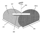
도 2는 O2/N2 반응성 플라즈마 스퍼터 플룸(plume) 중에서 Li3P 스퍼터 표적으로부터 수행되는 전해질 막의 스퍼터 증착의 실시양태를 예시한 것이며, 여기에서는 기판이 침지되고, 이어서 그 기판에 전해질 막이 증착된다.FIG. 2 illustrates an embodiment of sputter deposition of an electrolyte membrane performed from a Li 3 P sputter target in an O 2 / N 2 reactive plasma sputter plume, in which a substrate is immersed, followed by deposition of an electrolyte film on the substrate. do.
도 3은 LixP 상과 Li2O 상으로 구성되는 복합 스퍼터 표적으로부터 수행되는 전해질 막의 스퍼터 증착의 실시양태를 예시한 것이다.FIG. 3 illustrates an embodiment of sputter deposition of an electrolyte membrane performed from a composite sputter target consisting of a Li x P phase and a Li 2 O phase.
도 4는 Li2O가 Li3N으로 대체될 때 도 3의 스퍼터 증착의 실시양태를 예시한 것이다.FIG. 4 illustrates an embodiment of the sputter deposition of FIG. 3 when Li 2 O is replaced with Li 3 N. FIG.
도 5는 기판 상에서 전해질 막의 스퍼터 증착의 실시양태를 예시한 것이며, 여기서 기판은 2가지 상이한 스퍼터 표적으로부터 형성된 2가지 플라즈마 중에 침진된다. 5 illustrates an embodiment of sputter deposition of an electrolyte film on a substrate, where the substrate is deposited in two plasmas formed from two different sputter targets.
도 6은 스퍼터 증착의 플라즈마 스퍼터 플룸과 저항 증발 공정의 증발 플룸 둘 다를 기판 상에 유도함으로써 형성되는 기판 상의 전해질 막의 증착의 실시양태를 예시한 것이다. FIG. 6 illustrates an embodiment of deposition of an electrolyte film on a substrate formed by inducing both a plasma sputter plume of sputter deposition and an evaporation plume of a resistive evaporation process onto the substrate.
도 7은 전해질 막의 스퍼트 증착을 위한 두꺼운 금속성 스퍼터 표적의 방법의 실시양태를 예시한 것이다.FIG. 7 illustrates an embodiment of a method of thick metallic sputter target for sputter deposition of an electrolyte membrane.
바람직한 실시양태에 관한 상세한 설명Detailed Description of the Preferred Embodiments
본 발명의 이들 양태 및 다른 양태는 첨부된 도면에서 예시되어 있는 예시적 실시양태와 관련하여 보다 상세히 이하에서 설명할 것이다.These and other aspects of the invention will be described in more detail below in connection with the exemplary embodiments illustrated in the accompanying drawings.
본 발명은 본원에 기술된 구체적 방법론, 화합물, 물질, 제조 기법, 용도 및 응용분야에 국한되지 않는 것으로 이해되어야 하며, 그 이유는 이들이 다양할 수 있기 때문이다. 또한, 본원에 사용된 용어론은 단지 구체적 실시양태만을 기술할 목적으로만 사용하고, 본 발명의 영역을 제한하고자 사용하는 것이 아님을 이해해야 한다. 본원에 그리고 첨부된 특허청구범위에 사용된 바와 같이, 단수형("a", "an" 및 "the")은 문맥이 달리 명백하게 지시하고 있지 않는 한 복수형에 대한 사항을 포함한다는 점을 반드시 유의해야 한다. 따라서, 예를 들면,"요소"에 대한 사항은 하나 이상의 요소에 대한 사항이며, 해당 기술 분야의 당업자에게 잘 알려진 그 등가물을 포함한다. 유사하게, 다른 예를 들면, "단계" 또는 "수단"에 대한 사항은 하나 이상의 단계 또는 수단에 대한 사항이며, 하부 단계 및 종속 수단을 포함할 수 있다. 사용된 모든 접속사는 가능한 가장 포괄적인 의미로 이해되어야 한다. 따라서, 단어 "또는"는 문맥이 달리 분명하게 지시하고 있지 않는 한 "배타적 논리 합(logic exlusive or)"의 정의보다는 오히려 "논리적 합(logic or)"의 정의를 갖는 것으로 이해되어야 한다. 본원에 기술된 구조는 또한 그러한 구조의 기능성 등가물을 이미하는 것으로도 이해되어야 한다. 근사치를 나타내는 것으로 해석될 수 있는 언어는 문맥이 달리 지시하고 있지 않는 한 그러한 근사치로 이해되어야 한다.It is to be understood that the present invention is not limited to the specific methodologies, compounds, materials, preparation techniques, uses and applications described herein, as these may vary. It is also to be understood that the terminology used herein is for the purpose of describing particular embodiments only and is not intended to be limiting of the scope of the invention. As used herein and in the appended claims, it is to be noted that the singular forms “a,” “an,” and “the” include plural forms unless the context clearly dictates otherwise. do. Thus, for example, reference to "an element" refers to one or more elements and includes equivalents well known to those skilled in the art. Similarly, for example, the term "step" or "means" refers to one or more steps or means, and may include substeps and dependent means. All conjunctions used should be understood in the most comprehensive sense possible. Thus, the word "or" should be understood to have the definition of "logic or" rather than the definition of "logic exlusive or" unless the context clearly dictates otherwise. It is to be understood that the structures described herein also already possess functional equivalents of such structures. Languages that can be interpreted as representing approximations should be understood as such approximations unless the context indicates otherwise.
달리 정의되어 있지 않는 한, 본원에 사용된 모든 기술 및 과학 용어는 본 발명이 속하는 기술 분야의 당업자에 의해 일반적으로 이해되고 있는 바와 같이 동일한 의미를 갖는다. 본원에 기술된 것들과 유시하거나 동등한 임의의 방법, 기법, 장치 또는 물질이 본 발명의 실시 또는 시험에서 이용될 수 있다고 해도, 바람직한 방법, 기법, 장치 및 물질이 기술되어 있다. 본원에 기술된 구조는 또한 그러한 구조의 기능성 등가물을 언급한 것으로 이해해야 한다. 개시내용 및 특허청구범위의 문맥이 달리 특정하고 있지 않는 한, 예를 들면, 용어 "표적" 또는 "표적 타일"은 교환가능하게 사용될 수 있다.Unless defined otherwise, all technical and scientific terms used herein have the same meaning as commonly understood by one of ordinary skill in the art to which this invention belongs. Although any methods, techniques, devices or materials similar or equivalent to those described herein can be used in the practice or testing of the present invention, preferred methods, techniques, devices and materials are described. It is to be understood that the structures described herein also refer to functional equivalents of such structures. Unless the context of the disclosure and the claims is otherwise specified, for example, the terms "target" or "target tile" may be used interchangeably.
확인된 모든 특허 및 다른 공개물은 예를 들어 본 발명과 관련하여 이용될 수 있는 그러한 공개물에 기술된 방법론을 기술 및 개시할 목적으로 본원에 참고 인용되어 있다. 이러한 공개물은 단지 본 발명의 출원일 이전의 개시내용에 대해서만 제공되어 있다. 이와 관련하여, 본 발명자들은 선행 발명의 덕분으로 또는 임의의 다른 이유로 그러한 개시내용을 추정하도록 권한을 부여 받고 있지 않다는 허가로서 해석되어야 할 어떠한 사항도 없다. All patents and other publications identified are incorporated herein by reference for the purpose of describing and disclosing the methodology described in, for example, those publications that may be employed in connection with the present invention. Such publications are provided only for disclosures prior to the filing date of the present invention. In this regard, there is nothing that should be construed as an admission that the inventors are not authorized to estimate such disclosure by virtue of prior invention or for any other reason.
도 1은 본 발명의 일부 실시양태에 따른 박막 전기화학 에너지 저장 및 전환 장치에 사용하기 위한 리튬 이온 박막 전해질을 제조하기 위한 예시적 공정(100)의 실시양태를 예시한 것이다. 공정(100)은 예를 들어 기계적으로 강하고 실질적으로 전도성인 스퍼터 표적을 제조하는 단계(단계 101), 진공 증착 체임버를 제공하는 단계(단계 103), 그 기계적으로 강하고 실질적으로 전도성인 스퍼터 표적을 스퍼터링하는 단계(단계 105), 및 반응성 스퍼터 가스 대기 중에서 리튬 이온 박막 전해질을 증착시키는 단계(단계 107)를 포함한다. 1 illustrates an embodiment of an
단계(101)에서, 본 발명의 실시양태에 따르면, 스퍼터 표적은 실온에서 약 10-4 S/cm 이상의 전도도를 지닌 전기 전도성 또는 적어도 반전도성 표적 물질로부터 제조된다. 본 발명의 경우, 그 전도도는 실온에서 10 -8S/cm 이상인 것이 바람직하고, 실온에서 1 S/cm 이상인 것이 가장 바람직하다. 스퍼터 표적에 적합한 물질을 사용하고 그 물질을 반응성 가스 환경에서 작동시킴으로써, 전기 절연성이지만 리튬 이온 전도성인 막이 증착될 수 있다. 이러한 효과는 반응성 스퍼터 가스 환경을 이용함으로써 주입된 표적 물질이 서로 반응하고 스퍼트 플라즈마의 중성 및/또는 이온화 구성성분의 일부 하부세트와 반응하여 기판 상에 신규한 화학적 화합물을 형성시키는 것에 의존한다. 단계(107)에서, 반응성 스퍼터 가스 대기 중에서의 증착은 리튬 이온 전도성 스퍼터 표적으로부터 스퍼터링된 물질을 전기 절연성의 리튬 이온 전도성 저해질 막으로 전환시킬 수 있다. 단계(107)에서, 가능한 기체 구성성분은 화학적 원소 또는 화학적 화합물로서 가스 형태로 스퍼터 반응기 내로 도입되는 산소, 질소, 불소, 염소, 브롬, 요오드, 황, 설레늄, 텔루르, 인, 비소, 안티몬, 비스무트, 납, 탄소, 수소, 규소, 리튬, 나트륨, 마그네슘, 및 지르코늄을 포함한다. 가능한 표적 구성성분은 리튬, 인, 산소, 질소, 불소, 염소, 브롬, 요오드, 황, 셀레늄, 텔루르, 비소, 안티몬, 비스무트, 납, 탄소, 수소, 규소, 나트륨, 마그네슘 및 지르코늄 뿐만 아니라 리튬 포스페이트(Li3PO4), 질화 리튬 포스페이트, 리튬 포스파이드 및 서브-포스파이드(LixP, 1 ≤ x ≤ 100), 리튬 니트라이드 및 서브-니트라이드(LixN, 3 ≤ x ≤ 100), 인 옥사이드 및 서브-옥사이드(POx, x ≤ 2.5), 인 니트라이드 및 서브-니트라이드(PNx, x ≤ 1.7), 및 리튬 옥사이드 및 서브-옥사이드(LixO, 1 ≤ x ≤ 100)으로 이루어진 군으로부터 선택된 물질을 포함한다. 그 물질 시스템은 또한 스퍼터 가스와의 반응 결과로서 표적의 표면 상에 형성할 수 있는 임의의 절연 막이 실질적으로 후속 증착을 방해하지 않도록 선택되기도 한다. 스퍼터링된 구성성분 및 가스 구성성분이 전해질 막으로 전환되는 것을 유도하는 반응은 그 막의 표면 상에서 막이 증착됨에 따라 발생한다. In
표적을 전기 전도성으로 만들기 위해서, 표적 여기의 유형은 RF 전력에 더 이상 국한되지 않는다. 그러므로, 단계(103)에서, 제공된 진공 증착 체임버는 RF와 상용성을 갖지 않아야 하고, 이는 그렇지 않다면 대형 제조 도구에 곤란하기 때문이다. 유사하게도, 단계(105)에서 스퍼터링 공정은 보다 저렴한 DC 또는 펄스화 DC 전력 전자 기기를 사용하여 RF에 비하여 보다 높은 속도로 수행할 수 있다. 또한, 단계(107)에서 증착 공정은 종래의 RF 방법에 비하여 보다 신속하고 보다 저렴하게 완성할 수 있다. In order to make the target electrically conductive, the type of target excitation is no longer limited to RF power. Therefore, in
본 발명의 실시양태에 따르면, 단계(103, 105 및 107)는 RF(1MHz 내지 1GHz 범위), AC, 펄스화 DC 및 DC 전력의 임의 조합으로(단독으로 또는 함께 다양한 조합으로) 수행하여 관심 대상의 막을 생성할 수 있다. 또한, 단계(107)에서, 1 이상의 막 구성성분이 비-스퍼터 기법, 예컨대 열적 증발, 화학 기상 증착 또는 음극 아크 증착(chathodic arc deposition)을 이용하여 연속적으로 증착된다. 이러한 비-스퍼터링된 구성성분은 전기 절연 또는 전도성 공급원으로부터 증착될 수 있다. 후자 공곱원 물질은 증착이 공급원 물질의 화학적 반응성에 관하여 반응성 대기 중에서 수행되는 것을 포함하는 것이 가장 바람직하다.According to an embodiment of the invention, steps 103, 105 and 107 are of interest by performing any combination of RF (1 MHz to 1 GHz), AC, pulsed DC and DC power (alone or together in various combinations). Can create a film. Further, in
본 발명의 실시양태에 따르면, 단계(101)에서 스퍼터 표적은 단일 화합물, 다중 구성성분 복합재, 또는 유의적으로 상이한 조성을 지닌 표적의 범위에 속하는 표적 타일의 집합으로 제조될 수 있다. 모든 경우에서, 개별 타일 세그먼트는 300 cm2 보다 큰 것이 바람직하다. 1 이상의 상이한 유형의 표적이 소정의 막을 형성시키는데 필요하다면, 스퍼터링된 종들이 기판 상의 성장하는 막을 향해 동시적으로 유도되는 복수개 스퍼터 캐소드로부터의 증착 및/또는 임의의 표적 변환(switching)과 함께 기판 이동(translation)을 이용할 수 있다. 본 발명의 추가 이점은 전기 전도성 표적이 전형적인 전기 절연성 표적보다 더 열적 전도성을 기본적으로 갖는다는 점이다. 이러한 열적 전도도의 증가는 종래의 보다 얇은 것(0.6 cm)과 비교하여 보다 두꺼운 표적(5 cm 이하)의 수행을 허용함으로써, 표적 교체의 빈도를 감소시키게 된다(이는 전체적인 제조 비용을 감소시키게 된다).According to embodiments of the present invention, the sputter target in
다음의 실시예는 본 발명의 추가 이해를 제공하도록 포함하고, 본 명세서 내에 혼입되어 그 명세서의 일부를 구성하며, 본 발명의 예시적 실시양태를 예시한 것이다. The following examples are included to provide a further understanding of the present invention, incorporated into and constitute a part of this specification, and illustrate exemplary embodiments of the present invention.
실시예 1(도 2)은 공정(100)의 예시적 실시양태를 제공하며, 여기에서 조성 Li2.9PO3.3N0.45의 LIPON 전해질 막(205)은, 아르곤과 같은 불활성 가스를 첨가하거나 첨가하지 않으면서, 스퍼터링된 물질 및 산소와 잘소의 반응성 가스 혼합물을 포함하는 스퍼터 플라즈마 플룸(203) 중에 침지될 때 조성 Li3P의 반전도성 표적(201)으로부터 DC, 펄스화 DC 또는 RF 반응성 스퍼터링에 의해 기판 상에 증착할 수 있다. O2/N2 비율은 질소에 비하여 산소와 결합하는 증착 중인 Li 및 P 종의 보다 높은 친화성 때문에 1/100 미만으로 적합하게 할 수 있다. 진공 증착 반응기 내에서 주어진 산소/질소 비율(예를 들면, 1/1000)의 경우, 속도론적 및 열역학적 인자 둘 다는 성장하는 LixPOyNz 막에서의 최종 화학양론적 매개변수 x, y 및 z를 결정하게 된다. 특히 속도론적 매개변수로는 표적 스퍼터 전력(예를 들면, 직경이 10 인치인 Li3P 표적의 경우, 2000 W), 펄스화 듀티 사이클(예를 들면, 2 μs 전력 온 상태 및 2 μs 전력 오프 상태의 주기), 표적에서 기판에 이르는 거리(예를 들면, 7.5 cm), 증착 속도(예를 들면, 3 um/h), 기판 온도(예를 들면, 150℃), 기판 바이어스(예를 들면, -70 V), 질소 유속(예를 들면, 300 sccm), 및 산소 유속(예를 들면, 0.3 sscm, 0.1 부피% O2을 함유하는 N2 가스 공급을 통해 직접 달성될 수 있는 바와 같음)이 있다. 속도론적 매개변수와 관련하여, 성장하는 막 표면에서 열역학적 인자, 예컨대 기판 온도(다른 인자 중에서도 특히 스퍼터 표적 전력의 함수임) 및 산소/질소 비율은 성장하는 LIPON 막의 화학양론에서 중요한 역할을 한다.Example 1 (FIG. 2) provides an exemplary embodiment of
실시예 2(도 3)는 공정(100)의 예시적 실시양태를 제공하며, 여기서 Li2.9PO3.3N0.46의 LIPON 전해질 막(205)은, 리튬 농후 LixP(x ≫ 3)(305)와 Li20(307)로 구성되는 복합재 표적(301)(이것은 현미경 수준으로 또는 센티미터 척도로 복합화된 것임)으로부터, LixP 타일과 Li2O 타일을 서로 밀접하게 교대하여 배치함으로써 아르곤과 같은 불활성 가스를 첨가하거나 첨가하지 않으면서, 반응성의 적어도 질소 함유 스퍼터 플라즈마 플룸(303) 중에서 그러한 표적을 스퍼터링할 때, Li/P의 농도 비율이 약 2.9로 산출되고, O/P 비율이 약 3.3으로 산출되며, 동시에 N/P 비율이 약 0.46에 이르도록, DC, 펄스화 DC, AC 또는 RF 반응성 스퍼터링에 의해 증착할 수 있다. LixP(x ≫ 3)(305)와 Li20(307)의 현미경적 조성은 센티미터 척도 복합재에 비하여 바람직할 수 있으며, 이는 그것이 DC 또는 펄스 스퍼터 조건 하에 표적을 조작하는데 유용한 스퍼터 표적(301)의 반전도성 표면을 제공하기 때문이다. Example 2 (FIG. 3) provides an exemplary embodiment of
실시예 3(도 4)는 공정(100)의 예시적 실시양태를 제공하며, 여기서 스퍼터링 표적(401)은 실시예 2에 의해 예시된 바와 같은 LiO2(307) 대신에 Li3N(407)을 포함하고, 그와 같이 제조된 스퍼터 표적(401)은 적어도 질소 및 산소를 함유하는 플라즈마 플룸(403)에서 DC, 펄스화 DC, AC 또는 RF 스퍼터링된다.Example 3 (FIG. 4) provides an exemplary embodiment of
실시예 4는 공정(100)의 예시적 실시양태를 제공하며, 여기서 스퍼터링 표적은 실시예 3(도 4)에 의해 제공된 바와 같은 LixP(x ≥ 3) 대신에 P2O5을 포함하고, 그와 같이 제조된 스퍼터 표적은 적어도 질소를 함유하는 대기 중에서 DC, 펄스화 DC, AC 또는 RF 스퍼터링된다.Example 4 provides an exemplary embodiment of a
실시예 5는 공정(100)의 예시적 실시양태를 제공하며, 여기서 스퍼터링 표적은 실시예 4에 의해 제공된 바와 같은 P2O5 대신에 PN을 포함하고, 그와 같이 제조된 스퍼터 표적은 적어도 질소 및 산소를 함유하는 대기 중에서 DC, 펄스화 DC, AC 또는 RF 스퍼터링된다.Example 5 provides an exemplary embodiment of a
실시예 6은 공정(100)의 예시적 실시양태를 제공하며, 여기서 스퍼터링 표적은 금속성 리튬과 PN의 현미경적 복합재로부터 제조되고, 그와 같이 제조된 스퍼터 표적은 적어도 질소 및 산소를 함유하는 대기 중에서 DC, 펄스화 DC, AC 또는 RF 스퍼터링된다.Example 6 provides an exemplary embodiment of
실시예 7(도 5)는 공정(100)의 예시적 실시양태를 제공하며, 여기서 조성 Li2.9PO3.3N0.45의 LIPON 전해질 막(205)은 Li2.9PO3.3N0.45 전해질 막(205)이 성장하고 있는 기판(207)을 향해 스퍼터 플라즈마 플룸(503 및 503A) 둘 다가 그 기판으로 유도되는 2개 이상의 개별 스퍼터 표적(201, 501)으로부터 DC, AC 또는 RF 반응성 스퍼터링에 의해 증착할 수 있다. 제 1 스퍼터 표적(201)은 실시예 1(도 2)에 의해 제공된 바와 같이 제조할 수 있으며, 반면에 제2 스퍼터 표적(501)은 실시예 5에 의해 제공된 바와 같이 제조할 수 있다. 두께와 같은 다른 바람직한 균일성 특징 중에서도, 조성의 관점에서 막 균일성을 개선시키기 위해서, 기판(207)을, 그 수직 축(505) 둘레로 약간 상이하게 구성된 스퍼터 플라즈마 플룸(503 및 503 A) 내에서 회전시킬 수 있다. 제1 또는 제2 표적의 조성을 갖거나 또는 실시예 6에 제공된 표적과 같은 상이한 조성을 가질 수 있는 제3 스퍼터 표적이 진공 증착 반응기에 추가될 수 있다.Example 7 (FIG. 5) provides an exemplary embodiment of
실시예 8(도 6)은 공정(100)의 예시적 실시양태를 제공하며, 여기서 실시예 3(도 4)에 의해 제공된 LIPON 막(205)의 증착은 비-스퍼터 증착 공정(600), 예를 들면 Ta와 같은 적합한 도가니(601)로부터 금속성 리튬의 저항 증발에 의해 지지될 수 있다. 성장 중에 있는 LIPON 박(205)을 향해 유도되는 리튬 증기(603)는 그 막(205)의 리튬 농도를 조정할 뿐만 아니라 질소 및 산소 함유 대기(403 및 605) 중에서 리튬의 증착을 통해 그 막 내로 동시 증착되는 산소 및 질소의 농도를 다양하게 할 수 있다. 두께와 같은 다른 바람직한 균일성 특징 중에서도 특히 조성의 관점에서 막 균일성을 개선시키기 위해서, 기판(207)을, 그 중심 축(505) 둘레로 회전시킬 수 있다.Example 8 (FIG. 6) provides an exemplary embodiment of the
실시예 9는 공정(100)의 예시적 실시양태를 제공하며, 여기서 실시예 8에 의해 제공된 증착은 상이한 전기분해 활성 층들의 층상화된 스택을 형성하도록 하기 위해서 스퍼터 증착 또는 비-스퍼터 증착을 수초 내지 수분 동안 일시적으로 중단할 수 있는 셔터 메카니즘을 포함할 수 있으며, 상기 층들은 증착 중에 또는 증착 후에 LIPON 막의 열 처리에 의해 서로 확산될 수 있거나 확산되지 않을 수 있다.Example 9 provides an exemplary embodiment of a
실시예 10(도 7)은 공정(100)의 에시적 실시양태를 제공하며, 여기서 스퍼터 표적(701)은 Li50Al50 합금으로부터 제조되고, 스퍼터렝된 물질 및 F2-Ar의 반응성 가스 혼합물로 구성되는 스퍼터 플라즈마 플룸(703) 중에서 DC, 펄스화 DC, AC 또는 RF 스퍼터링에 의해 증착되며, 이는 결과적으로 유리상 리튬 이온 전해질 LiAlF4(705)을 형성하게 된다. 그 Li50Al50 합금은 금속 전도성이고, 아르곤과 같은 불활성 대기 중에서 표준 야금학적 방법에 의해 5 cm 이하의 두께로 제조될 수 있다. 그러한 두께 표적(701)의 스퍼터링은 여전히 가능하며, 이는 그 표적이 표적 배킹 플레이트(709)를 통해 표적 백사이드(707)의 냉각(711)을 허용하여 실현가능하게 잔류시키는 고 열전도도를 갖기 때문이다. 그러한 두께의 표적은 보다 얇은 표적보다 덜 빈번한 고체를 필요로 하며, 따라서 (i) 진공 증착 반응기의 유지보수 간격 및 (ii) 작동 비용을 감소시키게 된다.Example 10 (FIG. 7) provides an illustrative embodiment of
이상 기술된 실시양태 및 실시예는 단지 예시적인 것이다. 해당 기술 분야의 당업자라면, 본원에 구체적으로 기술된 실시양태로부터 유래된 다양한 변형예를 인식할 수 있을 것이며, 그 변형예는 본 발명의 개시내용의 영역에 속하는 것으로 의도된다. 이로써, 본 발명은 후술하는 특허청구범위에 의해서만 제한된다. 따라서, 본 발명은 본 발명의 변형예를 포함하는 것으로 의도되며, 단 그 변형예는 첨부된 특허청구범위 및 그 등가물의 영역 내에 속한다.The embodiments and examples described above are illustrative only. Those skilled in the art will recognize that various modifications derived from the embodiments specifically described herein are intended to fall within the scope of the present disclosure. As a result, the invention is limited only by the following claims. Thus, it is intended that the present invention include modifications of the invention, provided that the modifications fall within the scope of the appended claims and their equivalents.
Claims (26)
전도성 스퍼터 표적을 제공하는 단게,
진공 증착 반응기를 제공하는 단계,
상기 전도성 스퍼터 표적을 스퍼터링하는 단계, 및
반응성 스퍼터 가스 대기 중에서 리튬 이온 박막 전해질을 증착시키는 단계
를 포함하는 제조 방법.As a method for producing a lithium ion thin film electrolyte,
Providing a conductive sputter target,
Providing a vacuum deposition reactor,
Sputtering the conductive sputter target, and
Depositing a lithium ion thin film electrolyte in a reactive sputter gas atmosphere
≪ / RTI >
Applications Claiming Priority (2)
| Application Number | Priority Date | Filing Date | Title |
|---|---|---|---|
| US1603807P | 2007-12-21 | 2007-12-21 | |
| US61/016,038 | 2007-12-21 |
Related Child Applications (1)
| Application Number | Title | Priority Date | Filing Date |
|---|---|---|---|
| KR1020157027504A Division KR20150128817A (en) | 2007-12-21 | 2008-12-19 | Method for sputter targets for electrolyte films |
Publications (1)
| Publication Number | Publication Date |
|---|---|
| KR20100102180A true KR20100102180A (en) | 2010-09-20 |
Family
ID=40787306
Family Applications (2)
| Application Number | Title | Priority Date | Filing Date |
|---|---|---|---|
| KR1020107016420A KR20100102180A (en) | 2007-12-21 | 2008-12-19 | Method for sputter targets for electrolyte films |
| KR1020157027504A KR20150128817A (en) | 2007-12-21 | 2008-12-19 | Method for sputter targets for electrolyte films |
Family Applications After (1)
| Application Number | Title | Priority Date | Filing Date |
|---|---|---|---|
| KR1020157027504A KR20150128817A (en) | 2007-12-21 | 2008-12-19 | Method for sputter targets for electrolyte films |
Country Status (7)
| Country | Link |
|---|---|
| US (1) | US9334557B2 (en) |
| EP (1) | EP2225406A4 (en) |
| JP (1) | JP5551612B2 (en) |
| KR (2) | KR20100102180A (en) |
| CN (1) | CN101903560B (en) |
| TW (1) | TWI441937B (en) |
| WO (1) | WO2009086038A1 (en) |
Cited By (3)
| Publication number | Priority date | Publication date | Assignee | Title |
|---|---|---|---|---|
| KR20170090030A (en) * | 2016-01-28 | 2017-08-07 | 한국화학연구원 | Anti-reflection film with water repelling properties and Method of Manufacturing The Same |
| KR20180088777A (en) * | 2015-09-01 | 2018-08-07 | 한국화학연구원 | Method for manufacturing fluorocarbon thin film and fabrication equipment therof |
| KR20210089271A (en) * | 2013-09-05 | 2021-07-15 | 플란제 에스이 | Conductive target material |
Families Citing this family (48)
| Publication number | Priority date | Publication date | Assignee | Title |
|---|---|---|---|---|
| US20030002043A1 (en) * | 2001-04-10 | 2003-01-02 | Kla-Tencor Corporation | Periodic patterns and technique to control misalignment |
| US20080078268A1 (en) | 2006-10-03 | 2008-04-03 | H.C. Starck Inc. | Process for preparing metal powders having low oxygen content, powders so-produced and uses thereof |
| US20080145688A1 (en) | 2006-12-13 | 2008-06-19 | H.C. Starck Inc. | Method of joining tantalum clade steel structures |
| US8197894B2 (en) | 2007-05-04 | 2012-06-12 | H.C. Starck Gmbh | Methods of forming sputtering targets |
| US8246903B2 (en) | 2008-09-09 | 2012-08-21 | H.C. Starck Inc. | Dynamic dehydriding of refractory metal powders |
| US10156762B2 (en) | 2009-03-31 | 2018-12-18 | View, Inc. | Counter electrode for electrochromic devices |
| US10261381B2 (en) | 2009-03-31 | 2019-04-16 | View, Inc. | Fabrication of low defectivity electrochromic devices |
| US9261751B2 (en) | 2010-04-30 | 2016-02-16 | View, Inc. | Electrochromic devices |
| US11187954B2 (en) | 2009-03-31 | 2021-11-30 | View, Inc. | Electrochromic cathode materials |
| US8432603B2 (en) | 2009-03-31 | 2013-04-30 | View, Inc. | Electrochromic devices |
| US10591795B2 (en) | 2009-03-31 | 2020-03-17 | View, Inc. | Counter electrode for electrochromic devices |
| US10852613B2 (en) | 2009-03-31 | 2020-12-01 | View, Inc. | Counter electrode material for electrochromic devices |
| US12043890B2 (en) | 2009-03-31 | 2024-07-23 | View, Inc. | Electrochromic devices |
| US8582193B2 (en) | 2010-04-30 | 2013-11-12 | View, Inc. | Electrochromic devices |
| US8736947B2 (en) * | 2009-10-23 | 2014-05-27 | Applied Materials, Inc. | Materials and device stack for market viable electrochromic devices |
| TWI425103B (en) * | 2009-12-24 | 2014-02-01 | Metal Ind Res Anddevelopment Ct | Method and product of making zirconium - based metallic glass coating by multi - independent target |
| US9759975B2 (en) | 2010-04-30 | 2017-09-12 | View, Inc. | Electrochromic devices |
| TWI402370B (en) * | 2010-06-11 | 2013-07-21 | Ind Tech Res Inst | Method and apparatus for sputtering a coating containing a high vapor pressure material |
| CN103562431B (en) * | 2011-04-07 | 2016-05-11 | Sage电致变色显示有限公司 | Be used for the method for the improvement of controlling the lithium uniformity |
| US9771646B2 (en) | 2011-04-21 | 2017-09-26 | View, Inc. | Lithium sputter targets |
| WO2013003065A2 (en) | 2011-06-30 | 2013-01-03 | Soladigm, Inc. | Sputter target and sputtering methods |
| US8703233B2 (en) | 2011-09-29 | 2014-04-22 | H.C. Starck Inc. | Methods of manufacturing large-area sputtering targets by cold spray |
| US8864954B2 (en) * | 2011-12-23 | 2014-10-21 | Front Edge Technology Inc. | Sputtering lithium-containing material with multiple targets |
| US9077000B2 (en) | 2012-03-29 | 2015-07-07 | Front Edge Technology, Inc. | Thin film battery and localized heat treatment |
| FR2995454B1 (en) * | 2012-09-07 | 2014-08-22 | Commissariat Energie Atomique | PROCESS FOR PRODUCING LITHIUM ELECTROLYTE FOR SOLID MICRO-BATTERY |
| US9159964B2 (en) | 2012-09-25 | 2015-10-13 | Front Edge Technology, Inc. | Solid state battery having mismatched battery cells |
| US8753724B2 (en) | 2012-09-26 | 2014-06-17 | Front Edge Technology Inc. | Plasma deposition on a partially formed battery through a mesh screen |
| CN103066228A (en) * | 2012-12-27 | 2013-04-24 | 广东工业大学 | Preparation method for inorganic / organic multilayer composite separator |
| DE102014105531A1 (en) * | 2014-04-17 | 2015-10-22 | Schmid Energy Systems Gmbh | LiPON or LiPSON solid electrolyte layers and methods of making such layers |
| US11891327B2 (en) | 2014-05-02 | 2024-02-06 | View, Inc. | Fabrication of low defectivity electrochromic devices |
| EP3982195A1 (en) | 2014-09-05 | 2022-04-13 | View, Inc. | Counter electrode for electrochromic devices |
| EP4220291A3 (en) | 2014-11-26 | 2023-10-04 | View, Inc. | Counter electrode for electrochromic devices |
| US10008739B2 (en) | 2015-02-23 | 2018-06-26 | Front Edge Technology, Inc. | Solid-state lithium battery with electrolyte |
| ES2584961B1 (en) * | 2015-03-31 | 2017-07-04 | Advanced Nanotechnologies, S.L. | Fungible element for particle bombardment and etching determination procedure of said element |
| US20170073805A1 (en) * | 2015-04-30 | 2017-03-16 | E-Chromic Technologies, Inc. | Fabrication methodology for thin film lithium ion devices |
| WO2018005365A1 (en) | 2016-06-27 | 2018-01-04 | Board Of Regents, The University Of Texas System | Softening nerve cuff electrodes |
| CN107579275B (en) * | 2016-07-04 | 2022-02-11 | 松下知识产权经营株式会社 | Solid electrolyte containing oxynitride and secondary battery using the same |
| JP6667141B2 (en) * | 2016-07-04 | 2020-03-18 | パナソニックIpマネジメント株式会社 | Solid electrolyte containing oxynitride and secondary battery using the same |
| BE1025799B1 (en) * | 2017-12-18 | 2019-07-19 | Soleras Advanced Coatings Bvba | Injected lithium cobalt oxide targets |
| WO2020036927A1 (en) * | 2018-08-14 | 2020-02-20 | Massachusetts Institute Of Technology | Lithium-containing thin films |
| WO2020036936A1 (en) | 2018-08-14 | 2020-02-20 | Massachusetts Institute Of Technology | Methods of fabricating thin films comprising lithium-containing materials |
| CN110120547B (en) * | 2019-05-20 | 2021-03-09 | 河南固锂电技术有限公司 | Preparation method of electrolyte membrane for all-solid-state lithium ion battery and electrolyte membrane |
| CN110444751B (en) * | 2019-08-05 | 2021-06-01 | 张振刚 | Li-Si-N nano composite film, preparation method thereof, negative electrode structure and lithium battery |
| GB2588944B (en) * | 2019-11-15 | 2022-08-17 | Dyson Technology Ltd | Method of forming crystalline layer, method of forming a battery half cell |
| GB2588946B (en) * | 2019-11-15 | 2022-08-17 | Dyson Technology Ltd | Method of manufacturing crystalline material from different materials |
| JP6972427B2 (en) * | 2019-11-28 | 2021-11-24 | 株式会社アルバック | Film formation method |
| US20210184200A1 (en) * | 2019-12-11 | 2021-06-17 | GM Global Technology Operations LLC | Homogenous film coating of a particle |
| CN111430787B (en) * | 2020-03-03 | 2022-03-15 | 桂林电子科技大学 | Composite film solid electrolyte and preparation method and application thereof |
Family Cites Families (753)
| Publication number | Priority date | Publication date | Assignee | Title |
|---|---|---|---|---|
| US712316A (en) | 1899-10-26 | 1902-10-28 | Francois Loppe | Electric accumulator. |
| US2970180A (en) | 1959-06-17 | 1961-01-31 | Union Carbide Corp | Alkaline deferred action cell |
| US3309302A (en) | 1963-10-07 | 1967-03-14 | Varian Associates | Method of preparing an electron tube including sputtering a suboxide of titanium on dielectric components thereof |
| US3616403A (en) | 1968-10-25 | 1971-10-26 | Ibm | Prevention of inversion of p-type semiconductor material during rf sputtering of quartz |
| US3790432A (en) | 1971-12-30 | 1974-02-05 | Nasa | Reinforced polyquinoxaline gasket and method of preparing the same |
| US3797091A (en) | 1972-05-15 | 1974-03-19 | Du Pont | Terminal applicator |
| US3850604A (en) | 1972-12-11 | 1974-11-26 | Gte Laboratories Inc | Preparation of chalcogenide glass sputtering targets |
| US4111523A (en) | 1973-07-23 | 1978-09-05 | Bell Telephone Laboratories, Incorporated | Thin film optical waveguide |
| JPS559305Y2 (en) | 1974-12-10 | 1980-02-29 | ||
| US3939008A (en) | 1975-02-10 | 1976-02-17 | Exxon Research And Engineering Company | Use of perovskites and perovskite-related compounds as battery cathodes |
| US4127424A (en) | 1976-12-06 | 1978-11-28 | Ses, Incorporated | Photovoltaic cell array |
| US4082569A (en) | 1977-02-22 | 1978-04-04 | The United States Of America As Represented By The Administrator Of The National Aeronautics And Space Administration | Solar cell collector |
| DE2849294C3 (en) | 1977-11-22 | 1982-03-04 | Asahi Kasei Kogyo K.K., Osaka | Thin metal halide cell and process for its manufacture |
| IE49121B1 (en) | 1978-12-11 | 1985-08-07 | Triplex Safety Glass Co | Producing glass sheets of required curved shape |
| US4318938A (en) | 1979-05-29 | 1982-03-09 | The University Of Delaware | Method for the continuous manufacture of thin film solar cells |
| JPS5920374Y2 (en) | 1979-11-16 | 1984-06-13 | 技術資源開発株式会社 | rotor spray machine |
| JPS56156675U (en) | 1980-04-21 | 1981-11-21 | ||
| US4395713A (en) | 1980-05-06 | 1983-07-26 | Antenna, Incorporated | Transit antenna |
| US4442144A (en) | 1980-11-17 | 1984-04-10 | International Business Machines Corporation | Method for forming a coating on a substrate |
| US4467236A (en) | 1981-01-05 | 1984-08-21 | Piezo Electric Products, Inc. | Piezoelectric acousto-electric generator |
| US4328297A (en) | 1981-03-27 | 1982-05-04 | Yardngy Electric Corporation | Electrode |
| US5055704A (en) | 1984-07-23 | 1991-10-08 | Sgs-Thomson Microelectronics, Inc. | Integrated circuit package with battery housing |
| US4664993A (en) | 1981-08-24 | 1987-05-12 | Polaroid Corporation | Laminar batteries and methods of making the same |
| US4756717A (en) | 1981-08-24 | 1988-07-12 | Polaroid Corporation | Laminar batteries and methods of making the same |
| JPS58216476A (en) | 1982-06-11 | 1983-12-16 | Hitachi Ltd | Photoelectric-generating storage device |
| JPS5950027A (en) | 1982-09-13 | 1984-03-22 | Hitachi Ltd | Thin titanium disulfide film and its formation |
| US4518661A (en) | 1982-09-28 | 1985-05-21 | Rippere Ralph E | Consolidation of wires by chemical deposition and products resulting therefrom |
| US4437966A (en) | 1982-09-30 | 1984-03-20 | Gte Products Corporation | Sputtering cathode apparatus |
| JPS59217964A (en) | 1983-05-26 | 1984-12-08 | Hitachi Ltd | Positive electrode of thin film battery |
| JPS59227090A (en) | 1983-06-06 | 1984-12-20 | Hitachi Ltd | Nonvolatile memory device |
| DE3345659A1 (en) | 1983-06-16 | 1984-12-20 | Max-Planck-Gesellschaft zur Förderung der Wissenschaften e.V., 3400 Göttingen | ZIRCONIUM DIOXIDE CERAMIC BODY (ZRO (DOWN ARROW) 2 (DOWN ARROW)) AND METHOD FOR PRODUCING THE SAME |
| JPS6061217A (en) | 1983-09-14 | 1985-04-09 | シナージスティクス インダストリーズ リミテッド | Manufacture of expanded plastic product |
| DE3472398D1 (en) | 1983-10-17 | 1988-08-04 | Tosoh Corp | High-strength zirconia type sintered body and process for preparation thereof |
| JPS6068558U (en) | 1983-10-17 | 1985-05-15 | 株式会社リコー | Recording device agent transfer device |
| DE3417732A1 (en) | 1984-05-12 | 1986-07-10 | Leybold-Heraeus GmbH, 5000 Köln | METHOD FOR APPLYING SILICON-CONTAINING LAYERS TO SUBSTRATES BY CATODIZING AND SPRAYING CATODE FOR CARRYING OUT THE METHOD |
| GB8414878D0 (en) | 1984-06-11 | 1984-07-18 | Gen Electric Co Plc | Integrated optical waveguides |
| JPH06101335B2 (en) | 1984-11-26 | 1994-12-12 | 株式会社日立製作所 | All-solid-state lithium battery |
| US4785459A (en) | 1985-05-01 | 1988-11-15 | Baer Thomas M | High efficiency mode matched solid state laser with transverse pumping |
| JPS61269072A (en) | 1985-05-23 | 1986-11-28 | Nippon Denki Sanei Kk | Piezoelectric acceleration sensor |
| US4710940A (en) | 1985-10-01 | 1987-12-01 | California Institute Of Technology | Method and apparatus for efficient operation of optically pumped laser |
| JPH0336962Y2 (en) | 1985-10-31 | 1991-08-06 | ||
| US5173271A (en) | 1985-12-04 | 1992-12-22 | Massachusetts Institute Of Technology | Enhanced radiative zone-melting recrystallization method and apparatus |
| US5296089A (en) | 1985-12-04 | 1994-03-22 | Massachusetts Institute Of Technology | Enhanced radiative zone-melting recrystallization method and apparatus |
| US4964877A (en) | 1986-01-14 | 1990-10-23 | Wilson Greatbatch Ltd. | Non-aqueous lithium battery |
| JPS62267944A (en) | 1986-05-16 | 1987-11-20 | Hitachi Ltd | Magnetic recording medium |
| US4668593A (en) | 1986-08-29 | 1987-05-26 | Eltron Research, Inc. | Solvated electron lithium electrode for high energy density battery |
| US4977007A (en) | 1986-09-19 | 1990-12-11 | Matsushita Electrical Indust. Co. | Solid electrochemical element and production process therefor |
| JPH07107752B2 (en) | 1986-10-24 | 1995-11-15 | 株式会社日立製作所 | Optical information recording carrier |
| US4740431A (en) | 1986-12-22 | 1988-04-26 | Spice Corporation | Integrated solar cell and battery |
| JPS63215842A (en) | 1987-03-05 | 1988-09-08 | Takuma Co Ltd | Gas turbine generating system |
| JPS63290922A (en) | 1987-05-22 | 1988-11-28 | Matsushita Electric Works Ltd | Body weight meter |
| US4728588A (en) | 1987-06-01 | 1988-03-01 | The Dow Chemical Company | Secondary battery |
| JPH0610127Y2 (en) | 1987-08-21 | 1994-03-16 | 三菱自動車工業株式会社 | Electric heater for regeneration of exhaust gas aftertreatment device |
| US4865428A (en) | 1987-08-21 | 1989-09-12 | Corrigan Dennis A | Electrooptical device |
| JP2692816B2 (en) | 1987-11-13 | 1997-12-17 | 株式会社きもと | Thin primary battery |
| US4826743A (en) | 1987-12-16 | 1989-05-02 | General Motors Corporation | Solid-state lithium battery |
| US4878094A (en) | 1988-03-30 | 1989-10-31 | Minko Balkanski | Self-powered electronic component and manufacturing method therefor |
| US4915810A (en) | 1988-04-25 | 1990-04-10 | Unisys Corporation | Target source for ion beam sputter deposition |
| US4903326A (en) | 1988-04-27 | 1990-02-20 | Motorola, Inc. | Detachable battery pack with a built-in broadband antenna |
| US5096852A (en) | 1988-06-02 | 1992-03-17 | Burr-Brown Corporation | Method of making plastic encapsulated multichip hybrid integrated circuits |
| US5403680A (en) | 1988-08-30 | 1995-04-04 | Osaka Gas Company, Ltd. | Photolithographic and electron beam lithographic fabrication of micron and submicron three-dimensional arrays of electronically conductive polymers |
| FR2638764B1 (en) | 1988-11-04 | 1993-05-07 | Centre Nat Rech Scient | COMPOSITE ELEMENT COMPRISING A TITANIUM CHALCOGENIDE OR OXYCHALCOGENIDE LAYER, IN PARTICULAR AS A POSITIVE ELECTRODE IN A THIN-LAYER ELECTROCHEMICAL CELL |
| JPH02133599A (en) | 1988-11-11 | 1990-05-22 | Agency Of Ind Science & Technol | Production of iridium oxide film |
| JPH06100333B2 (en) | 1989-02-21 | 1994-12-12 | 三國工業株式会社 | Flame detection circuit for combustion equipment |
| JPH02230662A (en) | 1989-03-03 | 1990-09-13 | Tonen Corp | Lithium battery |
| US5006737A (en) | 1989-04-24 | 1991-04-09 | Motorola Inc. | Transformerless semiconductor AC switch having internal biasing means |
| US5100821A (en) | 1989-04-24 | 1992-03-31 | Motorola, Inc. | Semiconductor AC switch |
| US5217828A (en) | 1989-05-01 | 1993-06-08 | Brother Kogyo Kabushiki Kaisha | Flexible thin film cell including packaging material |
| US5540742A (en) | 1989-05-01 | 1996-07-30 | Brother Kogyo Kabushiki Kaisha | Method of fabricating thin film cells and printed circuit boards containing thin film cells using a screen printing process |
| JP2808660B2 (en) | 1989-05-01 | 1998-10-08 | ブラザー工業株式会社 | Method of manufacturing printed circuit board with built-in thin film battery |
| US5221891A (en) | 1989-07-31 | 1993-06-22 | Intermatic Incorporated | Control circuit for a solar-powered rechargeable power source and load |
| US5119269A (en) | 1989-08-23 | 1992-06-02 | Seiko Epson Corporation | Semiconductor with a battery unit |
| US5223457A (en) * | 1989-10-03 | 1993-06-29 | Applied Materials, Inc. | High-frequency semiconductor wafer processing method using a negative self-bias |
| US5792550A (en) | 1989-10-24 | 1998-08-11 | Flex Products, Inc. | Barrier film having high colorless transparency and method |
| JP2758948B2 (en) | 1989-12-15 | 1998-05-28 | キヤノン株式会社 | Thin film formation method |
| DE4022090A1 (en) | 1989-12-18 | 1991-06-20 | Forschungszentrum Juelich Gmbh | ELECTRO-OPTICAL COMPONENT AND METHOD FOR THE PRODUCTION THEREOF |
| US5252194A (en) | 1990-01-26 | 1993-10-12 | Varian Associates, Inc. | Rotating sputtering apparatus for selected erosion |
| US5169408A (en) | 1990-01-26 | 1992-12-08 | Fsi International, Inc. | Apparatus for wafer processing with in situ rinse |
| US5196374A (en) | 1990-01-26 | 1993-03-23 | Sgs-Thomson Microelectronics, Inc. | Integrated circuit package with molded cell |
| US5124782A (en) | 1990-01-26 | 1992-06-23 | Sgs-Thomson Microelectronics, Inc. | Integrated circuit package with molded cell |
| US5085904A (en) | 1990-04-20 | 1992-02-04 | E. I. Du Pont De Nemours And Company | Barrier materials useful for packaging |
| US5306569A (en) | 1990-06-15 | 1994-04-26 | Hitachi Metals, Ltd. | Titanium-tungsten target material and manufacturing method thereof |
| JP2755471B2 (en) | 1990-06-29 | 1998-05-20 | 日立電線株式会社 | Rare earth element doped optical waveguide and method of manufacturing the same |
| US5645626A (en) | 1990-08-10 | 1997-07-08 | Bend Research, Inc. | Composite hydrogen separation element and module |
| US5225288A (en) | 1990-08-10 | 1993-07-06 | E. I. Du Pont De Nemours And Company | Solvent blockers and multilayer barrier coatings for thin films |
| US5147985A (en) | 1990-08-14 | 1992-09-15 | The Scabbard Corporation | Sheet batteries as substrate for electronic circuit |
| JPH0458456U (en) | 1990-09-28 | 1992-05-19 | ||
| US5110694A (en) | 1990-10-11 | 1992-05-05 | The United States Of America As Represented By The Administrator Of The National Aeronautics And Space Administration | Secondary Li battery incorporating 12-Crown-4 ether |
| US5110696A (en) | 1990-11-09 | 1992-05-05 | Bell Communications Research | Rechargeable lithiated thin film intercalation electrode battery |
| US5273608A (en) | 1990-11-29 | 1993-12-28 | United Solar Systems Corporation | Method of encapsulating a photovoltaic device |
| US5493177A (en) | 1990-12-03 | 1996-02-20 | The Regents Of The University Of California | Sealed micromachined vacuum and gas filled devices |
| US5057385A (en) | 1990-12-14 | 1991-10-15 | Hope Henry F | Battery packaging construction |
| NL9002844A (en) | 1990-12-21 | 1992-07-16 | Philips Nv | SYSTEM INCLUDING A DEVICE AND A CASSETTE, AND A DEVICE AND A CASSETTE SUITABLE FOR USE IN SUCH A SYSTEM. |
| CA2056139C (en) | 1991-01-31 | 2000-08-01 | John C. Bailey | Electrochromic thin film state-of-charge detector for on-the-cell application |
| US5227264A (en) | 1991-02-14 | 1993-07-13 | Hydro-Quebec | Device for packaging a lithium battery |
| US6110531A (en) | 1991-02-25 | 2000-08-29 | Symetrix Corporation | Method and apparatus for preparing integrated circuit thin films by chemical vapor deposition |
| US5180645A (en) | 1991-03-01 | 1993-01-19 | Motorola, Inc. | Integral solid state embedded power supply |
| US5200029A (en) | 1991-04-25 | 1993-04-06 | At&T Bell Laboratories | Method of making a planar optical amplifier |
| US5119460A (en) | 1991-04-25 | 1992-06-02 | At&T Bell Laboratories | Erbium-doped planar optical device |
| US5107538A (en) | 1991-06-06 | 1992-04-21 | At&T Bell Laboratories | Optical waveguide system comprising a rare-earth Si-based optical device |
| US5208121A (en) | 1991-06-18 | 1993-05-04 | Wisconsin Alumni Research Foundation | Battery utilizing ceramic membranes |
| US5187564A (en) | 1991-07-26 | 1993-02-16 | Sgs-Thomson Microelectronics, Inc. | Application of laminated interconnect media between a laminated power source and semiconductor devices |
| US5153710A (en) | 1991-07-26 | 1992-10-06 | Sgs-Thomson Microelectronics, Inc. | Integrated circuit package with laminated backup cell |
| US5171413A (en) | 1991-09-16 | 1992-12-15 | Tufts University | Methods for manufacturing solid state ionic devices |
| US5196041A (en) | 1991-09-17 | 1993-03-23 | The Charles Stark Draper Laboratory, Inc. | Method of forming an optical channel waveguide by gettering |
| US5355089A (en) | 1992-07-22 | 1994-10-11 | Duracell Inc. | Moisture barrier for battery with electrochemical tester |
| JP2755844B2 (en) | 1991-09-30 | 1998-05-25 | シャープ株式会社 | Plastic substrate liquid crystal display |
| US5702829A (en) | 1991-10-14 | 1997-12-30 | Commissariat A L'energie Atomique | Multilayer material, anti-erosion and anti-abrasion coating incorporating said multilayer material |
| US5401595A (en) | 1991-12-06 | 1995-03-28 | Yuasa Corporation | Film type battery and layer-built film type battery |
| DK0546709T3 (en) | 1991-12-11 | 1997-10-13 | Mobil Oil Corp | Strong movie barrier |
| US5287427A (en) | 1992-05-05 | 1994-02-15 | At&T Bell Laboratories | Method of making an article comprising an optical component, and article comprising the component |
| US6144916A (en) | 1992-05-15 | 2000-11-07 | Micron Communications, Inc. | Itinerary monitoring system for storing a plurality of itinerary data points |
| US5497140A (en) | 1992-08-12 | 1996-03-05 | Micron Technology, Inc. | Electrically powered postage stamp or mailing or shipping label operative with radio frequency (RF) communication |
| SE470081B (en) | 1992-05-19 | 1993-11-01 | Gustavsson Magnus Peter M | Electrically heated garments or similar |
| US5776278A (en) | 1992-06-17 | 1998-07-07 | Micron Communications, Inc. | Method of manufacturing an enclosed transceiver |
| US5779839A (en) | 1992-06-17 | 1998-07-14 | Micron Communications, Inc. | Method of manufacturing an enclosed transceiver |
| US6741178B1 (en) | 1992-06-17 | 2004-05-25 | Micron Technology, Inc | Electrically powered postage stamp or mailing or shipping label operative with radio frequency (RF) communication |
| US6045652A (en) | 1992-06-17 | 2000-04-04 | Micron Communications, Inc. | Method of manufacturing an enclosed transceiver |
| DE4319878A1 (en) | 1992-06-17 | 1993-12-23 | Micron Technology Inc | High frequency identification system card - has integrated circuit chip or carrier layer sealed by top layer and coupled to batteries and antenna system |
| US5326652A (en) | 1993-01-25 | 1994-07-05 | Micron Semiconductor, Inc. | Battery package and method using flexible polymer films having a deposited layer of an inorganic material |
| US5338625A (en) | 1992-07-29 | 1994-08-16 | Martin Marietta Energy Systems, Inc. | Thin film battery and method for making same |
| US7158031B2 (en) | 1992-08-12 | 2007-01-02 | Micron Technology, Inc. | Thin, flexible, RFID label and system for use |
| JP3214910B2 (en) | 1992-08-18 | 2001-10-02 | 富士通株式会社 | Manufacturing method of planar waveguide optical amplifier |
| US5538796A (en) | 1992-10-13 | 1996-07-23 | General Electric Company | Thermal barrier coating system having no bond coat |
| US5597661A (en) | 1992-10-23 | 1997-01-28 | Showa Denko K.K. | Solid polymer electrolyte, battery and solid-state electric double layer capacitor using the same as well as processes for the manufacture thereof |
| JP3231900B2 (en) | 1992-10-28 | 2001-11-26 | 株式会社アルバック | Film forming equipment |
| US5326653A (en) | 1992-10-29 | 1994-07-05 | Valence Technology, Inc. | Battery unit with reinforced current collector tabs and method of making a battery unit having strengthened current collector tabs |
| JP3214107B2 (en) | 1992-11-09 | 2001-10-02 | 富士電機株式会社 | Battery mounted integrated circuit device |
| US5942089A (en) | 1996-04-22 | 1999-08-24 | Northwestern University | Method for sputtering compounds on a substrate |
| JPH06158308A (en) | 1992-11-24 | 1994-06-07 | Hitachi Metals Ltd | Target for sputtering for indium-tin oxide film and its production |
| US5279624A (en) | 1992-11-27 | 1994-01-18 | Gould Inc. | Solder sealed solid electrolyte cell housed within a ceramic frame and the method for producing it |
| US5307240A (en) | 1992-12-02 | 1994-04-26 | Intel Corporation | Chiplid, multichip semiconductor package design concept |
| US6022458A (en) | 1992-12-07 | 2000-02-08 | Canon Kabushiki Kaisha | Method of production of a semiconductor substrate |
| AU669754B2 (en) | 1992-12-18 | 1996-06-20 | Becton Dickinson & Company | Barrier coating |
| US5303319A (en) | 1992-12-28 | 1994-04-12 | Honeywell Inc. | Ion-beam deposited multilayer waveguides and resonators |
| SE500725C2 (en) | 1992-12-29 | 1994-08-15 | Volvo Ab | Device at panels for vehicles |
| US5427669A (en) | 1992-12-30 | 1995-06-27 | Advanced Energy Industries, Inc. | Thin film DC plasma processing system |
| US5718813A (en) | 1992-12-30 | 1998-02-17 | Advanced Energy Industries, Inc. | Enhanced reactive DC sputtering system |
| US5547780A (en) | 1993-01-18 | 1996-08-20 | Yuasa Corporation | Battery precursor and a battery |
| US5300461A (en) | 1993-01-25 | 1994-04-05 | Intel Corporation | Process for fabricating sealed semiconductor chip using silicon nitride passivation film |
| US5338624A (en) | 1993-02-08 | 1994-08-16 | Globe-Union Inc. | Thermal management of rechargeable batteries |
| JPH06279185A (en) | 1993-03-25 | 1994-10-04 | Canon Inc | Forming method of diamond crystal and diamond crystal film |
| US5262254A (en) | 1993-03-30 | 1993-11-16 | Valence Technology, Inc. | Positive electrode for rechargeable lithium batteries |
| US5302474A (en) | 1993-04-02 | 1994-04-12 | Valence Technology, Inc. | Fullerene-containing cathodes for solid electrochemical cells |
| US5613995A (en) | 1993-04-23 | 1997-03-25 | Lucent Technologies Inc. | Method for making planar optical waveguides |
| US5665490A (en) | 1993-06-03 | 1997-09-09 | Showa Denko K.K. | Solid polymer electrolyte, battery and solid-state electric double layer capacitor using the same as well as processes for the manufacture thereof |
| US5464692A (en) | 1993-06-17 | 1995-11-07 | Quality Manufacturing Incorporated | Flexible masking tape |
| DE69426003T2 (en) | 1993-07-28 | 2001-05-17 | Asahi Glass Co. Ltd., Tokio/Tokyo | Sputtering method and apparatus |
| US5499207A (en) | 1993-08-06 | 1996-03-12 | Hitachi, Ltd. | Semiconductor memory device having improved isolation between electrodes, and process for fabricating the same |
| US5599355A (en) | 1993-08-20 | 1997-02-04 | Nagasubramanian; Ganesan | Method for forming thin composite solid electrolyte film for lithium batteries |
| US5360686A (en) | 1993-08-20 | 1994-11-01 | The United States Of America As Represented By The National Aeronautics And Space Administration | Thin composite solid electrolyte film for lithium batteries |
| JP2642849B2 (en) | 1993-08-24 | 1997-08-20 | 株式会社フロンテック | Thin film manufacturing method and manufacturing apparatus |
| US5478456A (en) | 1993-10-01 | 1995-12-26 | Minnesota Mining And Manufacturing Company | Sputtering target |
| US5314765A (en) * | 1993-10-14 | 1994-05-24 | Martin Marietta Energy Systems, Inc. | Protective lithium ion conducting ceramic coating for lithium metal anodes and associate method |
| DE69430230T2 (en) | 1993-10-14 | 2002-10-31 | Mega Chips Corp., Osaka | Method and device for producing a single-crystal thin film |
| US5411537A (en) | 1993-10-29 | 1995-05-02 | Intermedics, Inc. | Rechargeable biomedical battery powered devices with recharging and control system therefor |
| US5445856A (en) | 1993-11-10 | 1995-08-29 | Chaloner-Gill; Benjamin | Protective multilayer laminate for covering an electrochemical device |
| US5738731A (en) | 1993-11-19 | 1998-04-14 | Mega Chips Corporation | Photovoltaic device |
| US5512387A (en) | 1993-11-19 | 1996-04-30 | Ovonic Battery Company, Inc. | Thin-film, solid state battery employing an electrically insulating, ion conducting electrolyte material |
| US5985485A (en) | 1993-11-19 | 1999-11-16 | Ovshinsky; Stanford R. | Solid state battery having a disordered hydrogenated carbon negative electrode |
| US5433835B1 (en) | 1993-11-24 | 1997-05-20 | Applied Materials Inc | Sputtering device and target with cover to hold cooling fluid |
| US5487822A (en) | 1993-11-24 | 1996-01-30 | Applied Materials, Inc. | Integrated sputtering target assembly |
| US5387482A (en) | 1993-11-26 | 1995-02-07 | Motorola, Inc. | Multilayered electrolyte and electrochemical cells used same |
| US5654984A (en) | 1993-12-03 | 1997-08-05 | Silicon Systems, Inc. | Signal modulation across capacitors |
| US5419982A (en) | 1993-12-06 | 1995-05-30 | Valence Technology, Inc. | Corner tab termination for flat-cell batteries |
| US6242128B1 (en) | 1993-12-06 | 2001-06-05 | Valence Technology, Inc. | Fastener system of tab bussing for batteries |
| US5569520A (en) | 1994-01-12 | 1996-10-29 | Martin Marietta Energy Systems, Inc. | Rechargeable lithium battery for use in applications requiring a low to high power output |
| JPH07224379A (en) | 1994-02-14 | 1995-08-22 | Ulvac Japan Ltd | Sputtering method and device therefor |
| US5961672A (en) | 1994-02-16 | 1999-10-05 | Moltech Corporation | Stabilized anode for lithium-polymer batteries |
| JP3836163B2 (en) | 1994-02-22 | 2006-10-18 | 旭硝子セラミックス株式会社 | Method for forming high refractive index film |
| US5561004A (en) | 1994-02-25 | 1996-10-01 | Bates; John B. | Packaging material for thin film lithium batteries |
| US5547781A (en) | 1994-03-02 | 1996-08-20 | Micron Communications, Inc. | Button-type battery with improved separator and gasket construction |
| US5464706A (en) | 1994-03-02 | 1995-11-07 | Dasgupta; Sankar | Current collector for lithium ion battery |
| US6408402B1 (en) | 1994-03-22 | 2002-06-18 | Hyperchip Inc. | Efficient direct replacement cell fault tolerant architecture |
| US5475528A (en) | 1994-03-25 | 1995-12-12 | Corning Incorporated | Optical signal amplifier glasses |
| US5470396A (en) | 1994-04-12 | 1995-11-28 | Amoco Corporation | Solar cell module package and method for its preparation |
| US5805223A (en) | 1994-05-25 | 1998-09-08 | Canon Kk | Image encoding apparatus having an intrapicture encoding mode and interpicture encoding mode |
| US5411592A (en) | 1994-06-06 | 1995-05-02 | Ovonic Battery Company, Inc. | Apparatus for deposition of thin-film, solid state batteries |
| KR100186895B1 (en) | 1994-06-13 | 1999-04-15 | 고다 시게노리 | Lithium ion-conductive glass film and thin carbon dioxide gas sensor using the same film |
| US5472795A (en) | 1994-06-27 | 1995-12-05 | Board Of Regents Of The University Of The University Of Wisconsin System, On Behalf Of The University Of Wisconsin-Milwaukee | Multilayer nanolaminates containing polycrystalline zirconia |
| US5457569A (en) | 1994-06-30 | 1995-10-10 | At&T Ipm Corp. | Semiconductor amplifier or laser having integrated lens |
| WO1996000996A1 (en) | 1994-06-30 | 1996-01-11 | The Whitaker Corporation | Planar hybrid optical amplifier |
| JP3407409B2 (en) | 1994-07-27 | 2003-05-19 | 富士通株式会社 | Manufacturing method of high dielectric constant thin film |
| US5504041A (en) | 1994-08-01 | 1996-04-02 | Texas Instruments Incorporated | Conductive exotic-nitride barrier layer for high-dielectric-constant materials |
| US6181283B1 (en) | 1994-08-01 | 2001-01-30 | Rangestar Wireless, Inc. | Selectively removable combination battery and antenna assembly for a telecommunication device |
| US5445906A (en) | 1994-08-03 | 1995-08-29 | Martin Marietta Energy Systems, Inc. | Method and system for constructing a rechargeable battery and battery structures formed with the method |
| US5458995A (en) | 1994-08-12 | 1995-10-17 | The United States Of America As Represented By The Secretary Of The Army | Solid state electrochemical cell including lithium iodide as an electrolyte additive |
| US5483613A (en) | 1994-08-16 | 1996-01-09 | At&T Corp. | Optical device with substrate and waveguide structure having thermal matching interfaces |
| US5909346A (en) | 1994-08-26 | 1999-06-01 | Aiwa Research & Development, Inc. | Thin magnetic film including multiple geometry gap structures on a common substrate |
| JP3042333B2 (en) | 1994-10-18 | 2000-05-15 | オムロン株式会社 | Electric signal displacement conversion device, equipment using the conversion device, and method of driving a fluid transfer device using the conversion device |
| US5437692A (en) | 1994-11-02 | 1995-08-01 | Dasgupta; Sankar | Method for forming an electrode-electrolyte assembly |
| US5498489A (en) | 1995-04-14 | 1996-03-12 | Dasgupta; Sankar | Rechargeable non-aqueous lithium battery having stacked electrochemical cells |
| JPH08148709A (en) | 1994-11-15 | 1996-06-07 | Mitsubishi Electric Corp | Thin solar cell manufacturing method and thin solar cell manufacturing apparatus |
| US7162392B2 (en) | 1994-11-21 | 2007-01-09 | Phatrat Technology, Inc. | Sport performance systems for measuring athletic performance, and associated methods |
| US6025094A (en) | 1994-11-23 | 2000-02-15 | Polyplus Battery Company, Inc. | Protective coatings for negative electrodes |
| CN1075243C (en) | 1994-12-28 | 2001-11-21 | 松下电器产业株式会社 | Capacity element of integrated circuit and manufacturing method thereof |
| US6204111B1 (en) | 1994-12-28 | 2001-03-20 | Matsushita Electronics Corporation | Fabrication method of capacitor for integrated circuit |
| US5555342A (en) | 1995-01-17 | 1996-09-10 | Lucent Technologies Inc. | Planar waveguide and a process for its fabrication |
| US5607789A (en) | 1995-01-23 | 1997-03-04 | Duracell Inc. | Light transparent multilayer moisture barrier for electrochemical cell tester and cell employing same |
| AU1834795A (en) | 1995-01-25 | 1996-08-14 | Applied Kotmatsu Technology, Inc. | Autoclave bonding of sputtering target assembly |
| US5755831A (en) | 1995-02-22 | 1998-05-26 | Micron Communications, Inc. | Method of forming a button-type battery and a button-type battery with improved separator construction |
| US6444750B1 (en) | 1995-03-06 | 2002-09-03 | Exxonmobil Oil Corp. | PVOH-based coating solutions |
| US5612153A (en) | 1995-04-13 | 1997-03-18 | Valence Technology, Inc. | Battery mask from radiation curable and thermoplastic materials |
| JPH10509773A (en) | 1995-04-25 | 1998-09-22 | ザ ビーオーシー グループ インコーポレイテッド | Sputtering apparatus and method for forming a dielectric layer on a substrate |
| US5771562A (en) | 1995-05-02 | 1998-06-30 | Motorola, Inc. | Passivation of organic devices |
| EP0834594B1 (en) | 1995-05-18 | 2004-11-10 | Asahi Glass Company Ltd. | Process for producing sputtering target |
| US5645960A (en) | 1995-05-19 | 1997-07-08 | The United States Of America As Represented By The Secretary Of The Air Force | Thin film lithium polymer battery |
| US5601952A (en) | 1995-05-24 | 1997-02-11 | Dasgupta; Sankar | Lithium-Manganese oxide electrode for a rechargeable lithium battery |
| US5758575A (en) | 1995-06-07 | 1998-06-02 | Bemis Company Inc. | Apparatus for printing an electrical circuit component with print cells in liquid communication |
| US5625202A (en) | 1995-06-08 | 1997-04-29 | University Of Central Florida | Modified wurtzite structure oxide compounds as substrates for III-V nitride compound semiconductor epitaxial thin film growth |
| US6265652B1 (en) | 1995-06-15 | 2001-07-24 | Kanegafuchi Kagaku Kogyo Kabushiki Kabushiki Kaisha | Integrated thin-film solar battery and method of manufacturing the same |
| KR100342189B1 (en) | 1995-07-12 | 2002-11-30 | 삼성전자 주식회사 | Method for producing rare earth elements-added optical fiber by using volatile composite |
| US6459418B1 (en) | 1995-07-20 | 2002-10-01 | E Ink Corporation | Displays combining active and non-active inks |
| US6639578B1 (en) | 1995-07-20 | 2003-10-28 | E Ink Corporation | Flexible displays |
| US6118426A (en) | 1995-07-20 | 2000-09-12 | E Ink Corporation | Transducers and indicators having printed displays |
| US5677784A (en) | 1995-07-24 | 1997-10-14 | Ellis D. Harris Sr. Family Trust | Array of pellicle optical gates |
| EP0761838B1 (en) | 1995-08-18 | 2001-08-08 | W.C. Heraeus GmbH & Co. KG | Sputtering target and method for its manufacturing |
| US5563979A (en) | 1995-08-31 | 1996-10-08 | Lucent Technologies Inc. | Erbium-doped planar optical device |
| US5582935A (en) | 1995-09-28 | 1996-12-10 | Dasgupta; Sankar | Composite electrode for a lithium battery |
| US5689522A (en) | 1995-10-02 | 1997-11-18 | The Regents Of The University Of California | High efficiency 2 micrometer laser utilizing wing-pumped Tm3+ and a laser diode array end-pumping architecture |
| US5716736A (en) | 1995-10-06 | 1998-02-10 | Midwest Research Institute | Solid lithium-ion electrolyte |
| US5616933A (en) | 1995-10-16 | 1997-04-01 | Sony Corporation | Nitride encapsulated thin film transistor fabrication technique |
| US5719976A (en) | 1995-10-24 | 1998-02-17 | Lucent Technologies, Inc. | Optimized waveguide structure |
| JP3298799B2 (en) | 1995-11-22 | 2002-07-08 | ルーセント テクノロジーズ インコーポレイテッド | Cladding pump fiber and its manufacturing method |
| US5686360A (en) | 1995-11-30 | 1997-11-11 | Motorola | Passivation of organic devices |
| US5811177A (en) | 1995-11-30 | 1998-09-22 | Motorola, Inc. | Passivation of electroluminescent organic devices |
| US5644207A (en) | 1995-12-11 | 1997-07-01 | The Johns Hopkins University | Integrated power source |
| US6608464B1 (en) | 1995-12-11 | 2003-08-19 | The Johns Hopkins University | Integrated power source layered with thin film rechargeable batteries, charger, and charge-control |
| US5897522A (en) | 1995-12-20 | 1999-04-27 | Power Paper Ltd. | Flexible thin layer open electrochemical cell and applications of same |
| GB9601236D0 (en) | 1996-01-22 | 1996-03-20 | Atraverda Ltd | Conductive coating |
| US5955161A (en) | 1996-01-30 | 1999-09-21 | Becton Dickinson And Company | Blood collection tube assembly |
| US5637418A (en) | 1996-02-08 | 1997-06-10 | Motorola, Inc. | Package for a flat electrochemical device |
| US5721067A (en) | 1996-02-22 | 1998-02-24 | Jacobs; James K. | Rechargeable lithium battery having improved reversible capacity |
| US5845990A (en) | 1996-03-11 | 1998-12-08 | Hilite Systems, L.L.C. | High signal lights for automotive vehicles |
| DE19609647A1 (en) * | 1996-03-12 | 1997-09-18 | Univ Sheffield | Hard coating |
| AU1978497A (en) | 1996-03-22 | 1997-10-10 | Materials Research Corporation | Method and apparatus for rf diode sputtering |
| FR2746934B1 (en) * | 1996-03-27 | 1998-05-07 | Saint Gobain Vitrage | ELECTROCHEMICAL DEVICE |
| US5930584A (en) | 1996-04-10 | 1999-07-27 | United Microelectronics Corp. | Process for fabricating low leakage current electrode for LPCVD titanium oxide films |
| JPH1010675A (en) | 1996-04-22 | 1998-01-16 | Fuji Photo Film Co Ltd | Recording material |
| JP3346167B2 (en) | 1996-05-27 | 2002-11-18 | 三菱マテリアル株式会社 | High-strength dielectric sputtering target, method for producing the same, and film |
| ATE282671T1 (en) | 1996-06-12 | 2004-12-15 | Treofan Germany Gmbh & Co Kg | CLEAR BARRIER COVERS WITH REDUCED THIN FILM INTERFERENCE |
| US5948464A (en) | 1996-06-19 | 1999-09-07 | Imra America, Inc. | Process of manufacturing porous separator for electrochemical power supply |
| EP0814529A1 (en) | 1996-06-19 | 1997-12-29 | Koninklijke Philips Electronics N.V. | Thin card containing flat accumulator and connecting devices |
| US5731661A (en) | 1996-07-15 | 1998-03-24 | Motorola, Inc. | Passivation of electroluminescent organic devices |
| US5855744A (en) | 1996-07-19 | 1999-01-05 | Applied Komatsu Technology, Inc. | Non-planar magnet tracking during magnetron sputtering |
| US5693956A (en) | 1996-07-29 | 1997-12-02 | Motorola | Inverted oleds on hard plastic substrate |
| JP3825843B2 (en) | 1996-09-12 | 2006-09-27 | キヤノン株式会社 | Solar cell module |
| CN1716663A (en) | 1996-10-11 | 2006-01-04 | 马萨诸塞州技术研究院 | Polymer electrolyte, intercalation compound and electrode for battery |
| US6007945A (en) | 1996-10-15 | 1999-12-28 | Electrofuel Inc. | Negative electrode for a rechargeable lithium battery comprising a solid solution of titanium dioxide and tin dioxide |
| JP3631341B2 (en) | 1996-10-18 | 2005-03-23 | Tdk株式会社 | Multilayer composite functional element and method for manufacturing the same |
| US5716728A (en) | 1996-11-04 | 1998-02-10 | Wilson Greatbatch Ltd. | Alkali metal electrochemical cell with improved energy density |
| US5841931A (en) | 1996-11-26 | 1998-11-24 | Massachusetts Institute Of Technology | Methods of forming polycrystalline semiconductor waveguides for optoelectronic integrated circuits, and devices formed thereby |
| US5783333A (en) | 1996-11-27 | 1998-07-21 | Polystor Corporation | Lithium nickel cobalt oxides for positive electrodes |
| EP0883137B1 (en) | 1996-12-11 | 2006-03-22 | Tonen Chemical Corporation | Thin aprotic electrolyte film, immobilized liquid film conductor, and polymer cell |
| US6144795A (en) | 1996-12-13 | 2000-11-07 | Corning Incorporated | Hybrid organic-inorganic planar optical waveguide device |
| US5842118A (en) | 1996-12-18 | 1998-11-24 | Micron Communications, Inc. | Communication system including diversity antenna queuing |
| US6289209B1 (en) | 1996-12-18 | 2001-09-11 | Micron Technology, Inc. | Wireless communication system, radio frequency communications system, wireless communications method, radio frequency communications method |
| JPH10195649A (en) | 1996-12-27 | 1998-07-28 | Sony Corp | Magnetron sputtering apparatus and method of manufacturing semiconductor device |
| US5705293A (en) | 1997-01-09 | 1998-01-06 | Lockheed Martin Energy Research Corporation | Solid state thin film battery having a high temperature lithium alloy anode |
| US5882812A (en) | 1997-01-14 | 1999-03-16 | Polyplus Battery Company, Inc. | Overcharge protection systems for rechargeable batteries |
| US5790489A (en) | 1997-01-21 | 1998-08-04 | Dell Usa, L.P. | Smart compact disk including a processor and a transmission element |
| JP4104187B2 (en) | 1997-02-06 | 2008-06-18 | 株式会社クレハ | Carbonaceous material for secondary battery electrode |
| US5944964A (en) | 1997-02-13 | 1999-08-31 | Optical Coating Laboratory, Inc. | Methods and apparatus for preparing low net stress multilayer thin film coatings |
| JPH10229201A (en) | 1997-02-14 | 1998-08-25 | Sony Corp | Manufacture of thin-film semiconductor device |
| JP3345878B2 (en) | 1997-02-17 | 2002-11-18 | 株式会社デンソー | Manufacturing method of electronic circuit device |
| US5847865A (en) | 1997-02-18 | 1998-12-08 | Regents Of The University Of Minnesota | Waveguide optical amplifier |
| US5970393A (en) | 1997-02-25 | 1999-10-19 | Polytechnic University | Integrated micro-strip antenna apparatus and a system utilizing the same for wireless communications for sensing and actuation purposes |
| JP3767151B2 (en) | 1997-02-26 | 2006-04-19 | ソニー株式会社 | Thin battery |
| JP3228168B2 (en) | 1997-02-28 | 2001-11-12 | 株式会社豊田中央研究所 | Rotation speed detection device and tire generation force detection device |
| JPH10302843A (en) | 1997-02-28 | 1998-11-13 | Mitsubishi Electric Corp | Adhesive for battery, battery using it, and its manufacture |
| JP3098204B2 (en) | 1997-03-07 | 2000-10-16 | ティーディーケイ株式会社 | Alloy target for magneto-optical recording, its manufacturing method and its reproducing method |
| JP2975907B2 (en) | 1997-03-10 | 1999-11-10 | 株式会社ワコー | Force / acceleration / magnetism detection device |
| US5952778A (en) | 1997-03-18 | 1999-09-14 | International Business Machines Corporation | Encapsulated organic light emitting device |
| JPH10265948A (en) | 1997-03-25 | 1998-10-06 | Rohm Co Ltd | Substrate for semiconductor device and method of manufacturing the same |
| ES2156334T3 (en) | 1997-03-27 | 2001-06-16 | Tno | FLAT WAVES GUIDE DOPED WITH ERBIO. |
| US6106933A (en) | 1997-04-03 | 2000-08-22 | Toray Industries, Inc. | Transparent gas barrier biaxially oriented polypropylene film, a laminate film, and a production method thereof |
| US6242132B1 (en) | 1997-04-16 | 2001-06-05 | Ut-Battelle, Llc | Silicon-tin oxynitride glassy composition and use as anode for lithium-ion battery |
| US5948215A (en) | 1997-04-21 | 1999-09-07 | Tokyo Electron Limited | Method and apparatus for ionized sputtering |
| EP0875952B1 (en) | 1997-04-23 | 2001-10-24 | Hydro-Quebec | Very thin solid state lithium cells and process of manufacture |
| US6422698B2 (en) | 1997-04-28 | 2002-07-23 | Binney & Smith Inc. | Ink jet marker |
| US6394598B1 (en) | 1997-04-28 | 2002-05-28 | Binney & Smith Inc. | Ink jet marker |
| US6329213B1 (en) | 1997-05-01 | 2001-12-11 | Micron Technology, Inc. | Methods for forming integrated circuits within substrates |
| US5882721A (en) | 1997-05-01 | 1999-03-16 | Imra America Inc | Process of manufacturing porous separator for electrochemical power supply |
| JP3290375B2 (en) | 1997-05-12 | 2002-06-10 | 松下電器産業株式会社 | Organic electroluminescent device |
| JP3045998B2 (en) | 1997-05-15 | 2000-05-29 | エフエムシー・コーポレイション | Interlayer compound and method for producing the same |
| US5895731A (en) | 1997-05-15 | 1999-04-20 | Nelson E. Smith | Thin-film lithium battery and process |
| US5830330A (en) | 1997-05-22 | 1998-11-03 | Tokyo Electron Limited | Method and apparatus for low pressure sputtering |
| US5977582A (en) | 1997-05-23 | 1999-11-02 | Lucent Technologies Inc. | Capacitor comprising improved TaOx -based dielectric |
| US6000603A (en) | 1997-05-23 | 1999-12-14 | 3M Innovative Properties Company | Patterned array of metal balls and methods of making |
| US6316563B2 (en) | 1997-05-27 | 2001-11-13 | Showa Denko K.K. | Thermopolymerizable composition and use thereof |
| US6077106A (en) | 1997-06-05 | 2000-06-20 | Micron Communications, Inc. | Thin profile battery mounting contact for printed circuit boards |
| US5865860A (en) | 1997-06-20 | 1999-02-02 | Imra America, Inc. | Process for filling electrochemical cells with electrolyte |
| CN1203462A (en) | 1997-06-20 | 1998-12-30 | 索尼株式会社 | Cell |
| US6051114A (en) | 1997-06-23 | 2000-04-18 | Applied Materials, Inc. | Use of pulsed-DC wafer bias for filling vias/trenches with metal in HDP physical vapor deposition |
| US5831262A (en) | 1997-06-27 | 1998-11-03 | Lucent Technologies Inc. | Article comprising an optical fiber attached to a micromechanical device |
| JP3813740B2 (en) | 1997-07-11 | 2006-08-23 | Tdk株式会社 | Substrates for electronic devices |
| US5982144A (en) | 1997-07-14 | 1999-11-09 | Johnson Research & Development Company, Inc. | Rechargeable battery power supply overcharge protection circuit |
| JP3335884B2 (en) | 1997-07-16 | 2002-10-21 | 株式会社荏原製作所 | Corrosion / corrosion analysis method |
| US6046514A (en) | 1997-07-25 | 2000-04-04 | 3M Innovative Properties Company | Bypass apparatus and method for series connected energy storage devices |
| US5973913A (en) | 1997-08-12 | 1999-10-26 | Covalent Associates, Inc. | Nonaqueous electrical storage device |
| KR100250855B1 (en) | 1997-08-28 | 2000-04-01 | 손욱 | Hybrid polymer electrolyte, preparation method thereof and lithium battery manufactured using same |
| US6252564B1 (en) | 1997-08-28 | 2001-06-26 | E Ink Corporation | Tiled displays |
| JPH11111273A (en) | 1997-09-29 | 1999-04-23 | Furukawa Battery Co Ltd:The | Manufacture of plate for lithium secondary battery and lithium secondary battery |
| US6156452A (en) | 1997-10-07 | 2000-12-05 | Matsushita Electric Indsutrial Co., Ltd. | Non-aqueous electrolyte secondary cell |
| US5916704A (en) | 1997-10-10 | 1999-06-29 | Ultralife Batteries | Low pressure battery vent |
| AU9451098A (en) | 1997-10-14 | 1999-05-03 | Patterning Technologies Limited | Method of forming an electronic device |
| US6982132B1 (en) | 1997-10-15 | 2006-01-03 | Trustees Of Tufts College | Rechargeable thin film battery and method for making the same |
| US6094292A (en) | 1997-10-15 | 2000-07-25 | Trustees Of Tufts College | Electrochromic window with high reflectivity modulation |
| US5985484A (en) | 1997-10-20 | 1999-11-16 | Amtek Research International Llc | Battery separation |
| US6084285A (en) | 1997-10-20 | 2000-07-04 | The Board Of Trustees Of The Leland Stanford Junior University | Lateral flux capacitor having fractal-shaped perimeters |
| WO1999021128A1 (en) | 1997-10-22 | 1999-04-29 | Cambridge Consultants Limited | Portable ic card |
| US5948562A (en) | 1997-11-03 | 1999-09-07 | Motorola, Inc. | Energy storage device |
| US6041734A (en) | 1997-12-01 | 2000-03-28 | Applied Materials, Inc. | Use of an asymmetric waveform to control ion bombardment during substrate processing |
| US6052397A (en) | 1997-12-05 | 2000-04-18 | Sdl, Inc. | Laser diode device having a substantially circular light output beam and a method of forming a tapered section in a semiconductor device to provide for a reproducible mode profile of the output beam |
| US6120890A (en) | 1997-12-12 | 2000-09-19 | Seagate Technology, Inc. | Magnetic thin film medium comprising amorphous sealing layer for reduced lithium migration |
| US5976327A (en) | 1997-12-12 | 1999-11-02 | Applied Materials, Inc. | Step coverage and overhang improvement by pedestal bias voltage modulation |
| US6042965A (en) | 1997-12-12 | 2000-03-28 | Johnson Research & Development Company, Inc. | Unitary separator and electrode structure and method of manufacturing separator |
| US6045942A (en) | 1997-12-15 | 2000-04-04 | Avery Dennison Corporation | Low profile battery and method of making same |
| JPH11204088A (en) | 1998-01-07 | 1999-07-30 | Toshiba Battery Co Ltd | Sheet battery |
| US6019284A (en) | 1998-01-27 | 2000-02-01 | Viztec Inc. | Flexible chip card with display |
| US6137671A (en) | 1998-01-29 | 2000-10-24 | Energenius, Inc. | Embedded energy storage device |
| US6608470B1 (en) | 1998-01-31 | 2003-08-19 | Motorola, Inc. | Overcharge protection device and methods for lithium based rechargeable batteries |
| WO1999041434A2 (en) | 1998-02-12 | 1999-08-19 | Acm Research, Inc. | Plating apparatus and method |
| US6402795B1 (en) | 1998-02-18 | 2002-06-11 | Polyplus Battery Company, Inc. | Plating metal negative electrodes under protective coatings |
| US6753108B1 (en) | 1998-02-24 | 2004-06-22 | Superior Micropowders, Llc | Energy devices and methods for the fabrication of energy devices |
| US6223317B1 (en) | 1998-02-28 | 2001-04-24 | Micron Technology, Inc. | Bit synchronizers and methods of synchronizing and calculating error |
| US6080508A (en) | 1998-03-06 | 2000-06-27 | Electrofuel Inc. | Packaging assembly for a lithium battery |
| US6610440B1 (en) | 1998-03-10 | 2003-08-26 | Bipolar Technologies, Inc | Microscopic batteries for MEMS systems |
| US6004660A (en) | 1998-03-12 | 1999-12-21 | E.I. Du Pont De Nemours And Company | Oxygen barrier composite film structure |
| US5889383A (en) | 1998-04-03 | 1999-03-30 | Advanced Micro Devices, Inc. | System and method for charging batteries with ambient acoustic energy |
| GB9808061D0 (en) | 1998-04-16 | 1998-06-17 | Cambridge Display Tech Ltd | Polymer devices |
| US6563998B1 (en) | 1999-04-15 | 2003-05-13 | John Farah | Polished polymide substrate |
| US6753114B2 (en) | 1998-04-20 | 2004-06-22 | Electrovaya Inc. | Composite electrolyte for a rechargeable lithium battery |
| US6175075B1 (en) | 1998-04-21 | 2001-01-16 | Canon Kabushiki Kaisha | Solar cell module excelling in reliability |
| US6169474B1 (en) | 1998-04-23 | 2001-01-02 | Micron Technology, Inc. | Method of communications in a backscatter system, interrogator, and backscatter communications system |
| US6459726B1 (en) | 1998-04-24 | 2002-10-01 | Micron Technology, Inc. | Backscatter interrogators, communication systems and backscatter communication methods |
| US6324211B1 (en) | 1998-04-24 | 2001-11-27 | Micron Technology, Inc. | Interrogators communication systems communication methods and methods of processing a communication signal |
| US6905578B1 (en) * | 1998-04-27 | 2005-06-14 | Cvc Products, Inc. | Apparatus and method for multi-target physical-vapor deposition of a multi-layer material structure |
| US6214061B1 (en) | 1998-05-01 | 2001-04-10 | Polyplus Battery Company, Inc. | Method for forming encapsulated lithium electrodes having glass protective layers |
| US6420961B1 (en) | 1998-05-14 | 2002-07-16 | Micron Technology, Inc. | Wireless communication systems, interfacing devices, communication methods, methods of interfacing with an interrogator, and methods of operating an interrogator |
| US6075973A (en) | 1998-05-18 | 2000-06-13 | Micron Technology, Inc. | Method of communications in a backscatter system, interrogator, and backscatter communications system |
| US6115616A (en) | 1998-05-28 | 2000-09-05 | International Business Machines Corporation | Hand held telephone set with separable keyboard |
| DE19824145A1 (en) | 1998-05-29 | 1999-12-16 | Siemens Ag | Integrated antenna arrangement for mobile telecommunications terminal |
| JP3126698B2 (en) | 1998-06-02 | 2001-01-22 | 富士通株式会社 | Sputter film forming method, sputter film forming apparatus, and semiconductor device manufacturing method |
| US6093944A (en) | 1998-06-04 | 2000-07-25 | Lucent Technologies Inc. | Dielectric materials of amorphous compositions of TI-O2 doped with rare earth elements and devices employing same |
| US7854684B1 (en) | 1998-06-24 | 2010-12-21 | Samsung Electronics Co., Ltd. | Wearable device |
| KR100287176B1 (en) | 1998-06-25 | 2001-04-16 | 윤종용 | Method for forming a capacitor using high temperature oxidation |
| US6058233A (en) | 1998-06-30 | 2000-05-02 | Lucent Technologies Inc. | Waveguide array with improved efficiency for wavelength routers and star couplers in integrated optics |
| GB9814123D0 (en) | 1998-07-01 | 1998-08-26 | British Gas Plc | Electrochemical fuel cell |
| EP0969521A1 (en) | 1998-07-03 | 2000-01-05 | ISOVOLTAÖsterreichische IsolierstoffwerkeAktiengesellschaft | Photovoltaic module and method of fabrication |
| DE19831719A1 (en) | 1998-07-15 | 2000-01-20 | Alcatel Sa | Process for the production of planar waveguide structures and waveguide structure |
| US6358810B1 (en) | 1998-07-28 | 2002-03-19 | Applied Materials, Inc. | Method for superior step coverage and interface control for high K dielectric capacitors and related electrodes |
| US6146225A (en) | 1998-07-30 | 2000-11-14 | Agilent Technologies, Inc. | Transparent, flexible permeability barrier for organic electroluminescent devices |
| US6129277A (en) | 1998-08-03 | 2000-10-10 | Privicon, Inc. | Card reader for transmission of data by sound |
| US6579728B2 (en) | 1998-08-03 | 2003-06-17 | Privicom, Inc. | Fabrication of a high resolution, low profile credit card reader and card reader for transmission of data by sound |
| US6160373A (en) | 1998-08-10 | 2000-12-12 | Dunn; James P. | Battery operated cableless external starting device and methods |
| JP2000067852A (en) | 1998-08-21 | 2000-03-03 | Pioneer Electronic Corp | Lithium secondary battery |
| KR100305903B1 (en) | 1998-08-21 | 2001-12-17 | 박호군 | Electrical and electronic devices with thin-film batteries connected vertically and integrated and methods for fabricating the same |
| US6480699B1 (en) | 1998-08-28 | 2002-11-12 | Woodtoga Holdings Company | Stand-alone device for transmitting a wireless signal containing data from a memory or a sensor |
| JP3386756B2 (en) | 1998-08-31 | 2003-03-17 | 松下電池工業株式会社 | Thin film forming method and thin film forming apparatus |
| US6210832B1 (en) | 1998-09-01 | 2001-04-03 | Polyplus Battery Company, Inc. | Mixed ionic electronic conductor coatings for redox electrodes |
| US6192222B1 (en) | 1998-09-03 | 2001-02-20 | Micron Technology, Inc. | Backscatter communication systems, interrogators, methods of communicating in a backscatter system, and backscatter communication methods |
| JP4014737B2 (en) | 1998-09-17 | 2007-11-28 | 昭和電工株式会社 | Thermally polymerizable composition and use thereof |
| US6236793B1 (en) | 1998-09-23 | 2001-05-22 | Molecular Optoelectronics Corporation | Optical channel waveguide amplifier |
| US6362916B2 (en) | 1998-09-25 | 2002-03-26 | Fiver Laboratories | All fiber gain flattening optical filter |
| US6159635A (en) | 1998-09-29 | 2000-12-12 | Electrofuel Inc. | Composite electrode including current collector |
| KR100283954B1 (en) | 1998-10-13 | 2001-03-02 | 윤종용 | Optical fiber for optical amplifier |
| US7323634B2 (en) | 1998-10-14 | 2008-01-29 | Patterning Technologies Limited | Method of forming an electronic device |
| KR100282487B1 (en) | 1998-10-19 | 2001-02-15 | 윤종용 | Cell Capacitor Using High-Dielectric Multilayer Film and Its Manufacturing Method |
| US6605228B1 (en) | 1998-10-19 | 2003-08-12 | Nhk Spring Co., Ltd. | Method for fabricating planar optical waveguide devices |
| JP4126711B2 (en) | 1998-10-23 | 2008-07-30 | ソニー株式会社 | Non-aqueous electrolyte battery |
| JP3830008B2 (en) | 1998-10-30 | 2006-10-04 | ソニー株式会社 | Non-aqueous electrolyte battery |
| US6157765A (en) | 1998-11-03 | 2000-12-05 | Lucent Technologies | Planar waveguide optical amplifier |
| KR100280705B1 (en) | 1998-11-05 | 2001-03-02 | 김순택 | Electrode active material composition for lithium ion polymer battery and manufacturing method of electrode plate for lithium ion polymer battery using same |
| US6797429B1 (en) | 1998-11-06 | 2004-09-28 | Japan Storage Battery Co, Ltd. | Non-aqueous electrolytic secondary cell |
| ATE333207T1 (en) | 1998-11-09 | 2006-08-15 | Ballard Power Systems | ELECTRICAL CONTACT DEVICE FOR A FUEL CELL |
| US6384573B1 (en) | 1998-11-12 | 2002-05-07 | James Dunn | Compact lightweight auxiliary multifunctional reserve battery engine starting system (and methods) |
| US6117279A (en) | 1998-11-12 | 2000-09-12 | Tokyo Electron Limited | Method and apparatus for increasing the metal ion fraction in ionized physical vapor deposition |
| JP2000162234A (en) | 1998-11-30 | 2000-06-16 | Matsushita Electric Ind Co Ltd | Piezoelectric sensor circuit |
| US6365300B1 (en) | 1998-12-03 | 2002-04-02 | Sumitomo Electric Industries, Ltd. | Lithium secondary battery |
| US6268695B1 (en) | 1998-12-16 | 2001-07-31 | Battelle Memorial Institute | Environmental barrier material for organic light emitting device and method of making |
| EP1145338B1 (en) | 1998-12-16 | 2012-12-05 | Samsung Display Co., Ltd. | Environmental barrier material for organic light emitting device and method of making |
| JP2000188099A (en) | 1998-12-22 | 2000-07-04 | Mitsubishi Chemicals Corp | Manufacture of thin film type battery |
| WO2000041256A1 (en) | 1999-01-08 | 2000-07-13 | Massachusetts Institute Of Technology | Electroactive material for secondary batteries and methods of preparation |
| GB9900396D0 (en) | 1999-01-08 | 1999-02-24 | Danionics As | Arrangements of electrochemical cells |
| JP4074418B2 (en) | 1999-01-11 | 2008-04-09 | 三菱化学株式会社 | Thin film type lithium secondary battery |
| US6379835B1 (en) | 1999-01-12 | 2002-04-30 | Morgan Adhesives Company | Method of making a thin film battery |
| US6290822B1 (en) | 1999-01-26 | 2001-09-18 | Agere Systems Guardian Corp. | Sputtering method for forming dielectric films |
| US6302939B1 (en) | 1999-02-01 | 2001-10-16 | Magnequench International, Inc. | Rare earth permanent magnet and method for making same |
| JP2000294291A (en) * | 1999-02-03 | 2000-10-20 | Sanyo Electric Co Ltd | Polymer electrolyte battery |
| US6306265B1 (en) | 1999-02-12 | 2001-10-23 | Applied Materials, Inc. | High-density plasma for ionized metal deposition capable of exciting a plasma wave |
| AU768057B2 (en) | 1999-02-25 | 2003-11-27 | Kaneka Corporation | Integrated thin-film solar battery |
| US6210544B1 (en) | 1999-03-08 | 2001-04-03 | Alps Electric Co., Ltd. | Magnetic film forming method |
| US6603391B1 (en) | 1999-03-09 | 2003-08-05 | Micron Technology, Inc. | Phase shifters, interrogators, methods of shifting a phase angle of a signal, and methods of operating an interrogator |
| US6356764B1 (en) | 1999-03-09 | 2002-03-12 | Micron Technology, Inc. | Wireless communication systems, interrogators and methods of communicating within a wireless communication system |
| EP1037293B1 (en) | 1999-03-16 | 2007-05-16 | Sumitomo Chemical Company, Limited | Non-aqueous electrolyte and lithium secondary battery using the same |
| US6277520B1 (en) | 1999-03-19 | 2001-08-21 | Ntk Powerdex, Inc. | Thin lithium battery with slurry cathode |
| US6280875B1 (en) | 1999-03-24 | 2001-08-28 | Teledyne Technologies Incorporated | Rechargeable battery structure with metal substrate |
| EP1039554B1 (en) | 1999-03-25 | 2003-05-14 | Kaneka Corporation | Method of manufacturing thin film solar cell-modules |
| US6160215A (en) | 1999-03-26 | 2000-12-12 | Curtin; Lawrence F. | Method of making photovoltaic device |
| US6148503A (en) | 1999-03-31 | 2000-11-21 | Imra America, Inc. | Process of manufacturing porous separator for electrochemical power supply |
| US6398824B1 (en) | 1999-04-02 | 2002-06-04 | Excellatron Solid State, Llc | Method for manufacturing a thin-film lithium battery by direct deposition of battery components on opposite sides of a current collector |
| US6242129B1 (en) | 1999-04-02 | 2001-06-05 | Excellatron Solid State, Llc | Thin lithium film battery |
| US6168884B1 (en) | 1999-04-02 | 2001-01-02 | Lockheed Martin Energy Research Corporation | Battery with an in-situ activation plated lithium anode |
| AU3985200A (en) | 1999-04-14 | 2000-11-14 | Power Paper Ltd. | Functionally improved battery and method of making same |
| US6855441B1 (en) | 1999-04-14 | 2005-02-15 | Power Paper Ltd. | Functionally improved battery and method of making same |
| US6416598B1 (en) | 1999-04-20 | 2002-07-09 | Reynolds Metals Company | Free machining aluminum alloy with high melting point machining constituent and method of use |
| KR100296741B1 (en) | 1999-05-11 | 2001-07-12 | 박호군 | Battery with trench structure and fabrication method |
| JP3736205B2 (en) | 1999-06-04 | 2006-01-18 | 三菱電機株式会社 | Battery power storage device |
| US6281142B1 (en) | 1999-06-04 | 2001-08-28 | Micron Technology, Inc. | Dielectric cure for reducing oxygen vacancies |
| US6046081A (en) | 1999-06-10 | 2000-04-04 | United Microelectronics Corp. | Method for forming dielectric layer of capacitor |
| US6133670A (en) | 1999-06-24 | 2000-10-17 | Sandia Corporation | Compact electrostatic comb actuator |
| US6413676B1 (en) | 1999-06-28 | 2002-07-02 | Lithium Power Technologies, Inc. | Lithium ion polymer electrolytes |
| JP2001021744A (en) | 1999-07-07 | 2001-01-26 | Shin Etsu Chem Co Ltd | Manufacture of optical waveguide substrate |
| JP2001020065A (en) | 1999-07-07 | 2001-01-23 | Hitachi Metals Ltd | Target for sputtering, its production and high melting point metal powder material |
| JP2001025666A (en) | 1999-07-14 | 2001-01-30 | Nippon Sheet Glass Co Ltd | Laminate and its production |
| US6290821B1 (en) | 1999-07-15 | 2001-09-18 | Seagate Technology Llc | Sputter deposition utilizing pulsed cathode and substrate bias power |
| KR100456647B1 (en) | 1999-08-05 | 2004-11-10 | 에스케이씨 주식회사 | Lithium ion polymer battery |
| US6249222B1 (en) | 1999-08-17 | 2001-06-19 | Lucent Technologies Inc. | Method and apparatus for generating color based alerting signals |
| US6344795B1 (en) | 1999-08-17 | 2002-02-05 | Lucent Technologies Inc. | Method and apparatus for generating temperature based alerting signals |
| US6356230B1 (en) | 1999-08-20 | 2002-03-12 | Micron Technology, Inc. | Interrogators, wireless communication systems, methods of operating an interrogator, methods of monitoring movement of a radio frequency identification device, methods of monitoring movement of a remote communication device and movement monitoring methods |
| US6414626B1 (en) | 1999-08-20 | 2002-07-02 | Micron Technology, Inc. | Interrogators, wireless communication systems, methods of operating an interrogator, methods of operating a wireless communication system, and methods of determining range of a remote communication device |
| US6664006B1 (en) | 1999-09-02 | 2003-12-16 | Lithium Power Technologies, Inc. | All-solid-state electrochemical device and method of manufacturing |
| US6537428B1 (en) | 1999-09-02 | 2003-03-25 | Veeco Instruments, Inc. | Stable high rate reactive sputtering |
| US6645675B1 (en) | 1999-09-02 | 2003-11-11 | Lithium Power Technologies, Inc. | Solid polymer electrolytes |
| US6392565B1 (en) | 1999-09-10 | 2002-05-21 | Eworldtrack, Inc. | Automobile tracking and anti-theft system |
| US6528212B1 (en) | 1999-09-13 | 2003-03-04 | Sanyo Electric Co., Ltd. | Lithium battery |
| US6344366B1 (en) | 1999-09-15 | 2002-02-05 | Lockheed Martin Energy Research Corporation | Fabrication of highly textured lithium cobalt oxide films by rapid thermal annealing |
| US6296949B1 (en) | 1999-09-16 | 2001-10-02 | Ga-Tek Inc. | Copper coated polyimide with metallic protective layer |
| JP4240679B2 (en) | 1999-09-21 | 2009-03-18 | ソニー株式会社 | Method for producing sputtering target |
| US6296967B1 (en) | 1999-09-24 | 2001-10-02 | Electrofuel Inc. | Lithium battery structure incorporating lithium pouch cells |
| TW457767B (en) | 1999-09-27 | 2001-10-01 | Matsushita Electric Works Ltd | Photo response semiconductor switch having short circuit load protection |
| JP4460742B2 (en) | 1999-10-01 | 2010-05-12 | 日本碍子株式会社 | Piezoelectric / electrostrictive device and manufacturing method thereof |
| US6368275B1 (en) | 1999-10-07 | 2002-04-09 | Acuson Corporation | Method and apparatus for diagnostic medical information gathering, hyperthermia treatment, or directed gene therapy |
| DE19948839A1 (en) | 1999-10-11 | 2001-04-12 | Bps Alzenau Gmbh | Conductive transparent layers and processes for their manufacture |
| US6500287B1 (en) | 1999-10-14 | 2002-12-31 | Forskarpatent I Uppsala Ab | Color-modifying treatment of thin films |
| US6573652B1 (en) | 1999-10-25 | 2003-06-03 | Battelle Memorial Institute | Encapsulated display devices |
| US6623861B2 (en) | 2001-04-16 | 2003-09-23 | Battelle Memorial Institute | Multilayer plastic substrates |
| US6413645B1 (en) | 2000-04-20 | 2002-07-02 | Battelle Memorial Institute | Ultrabarrier substrates |
| US20070196682A1 (en) | 1999-10-25 | 2007-08-23 | Visser Robert J | Three dimensional multilayer barrier and method of making |
| US6548912B1 (en) | 1999-10-25 | 2003-04-15 | Battelle Memorial Institute | Semicoductor passivation using barrier coatings |
| US7198832B2 (en) | 1999-10-25 | 2007-04-03 | Vitex Systems, Inc. | Method for edge sealing barrier films |
| US6866901B2 (en) | 1999-10-25 | 2005-03-15 | Vitex Systems, Inc. | Method for edge sealing barrier films |
| US6413285B1 (en) | 1999-11-01 | 2002-07-02 | Polyplus Battery Company | Layered arrangements of lithium electrodes |
| US6529827B1 (en) | 1999-11-01 | 2003-03-04 | Garmin Corporation | GPS device with compass and altimeter and method for displaying navigation information |
| US6413284B1 (en) | 1999-11-01 | 2002-07-02 | Polyplus Battery Company | Encapsulated lithium alloy electrodes having barrier layers |
| US6271793B1 (en) | 1999-11-05 | 2001-08-07 | International Business Machines Corporation | Radio frequency (RF) transponder (Tag) with composite antenna |
| CN1258830C (en) | 1999-11-11 | 2006-06-07 | 皇家菲利浦电子有限公司 | Lithium battery containing gel-electrolyte |
| US6340880B1 (en) | 1999-11-11 | 2002-01-22 | Mitsumi Electric Co., Ltd. | Method of protecting a chargeable electric cell |
| JP3999424B2 (en) | 1999-11-16 | 2007-10-31 | ローム株式会社 | Terminal board, battery pack provided with terminal board, and method of manufacturing terminal board |
| US6733924B1 (en) | 1999-11-23 | 2004-05-11 | Moltech Corporation | Lithium anodes for electrochemical cells |
| US6582481B1 (en) | 1999-11-23 | 2003-06-24 | Johnson Research & Development Company, Inc. | Method of producing lithium base cathodes |
| US6797428B1 (en) | 1999-11-23 | 2004-09-28 | Moltech Corporation | Lithium anodes for electrochemical cells |
| US7247408B2 (en) | 1999-11-23 | 2007-07-24 | Sion Power Corporation | Lithium anodes for electrochemical cells |
| US6511516B1 (en) | 2000-02-23 | 2003-01-28 | Johnson Research & Development Co., Inc. | Method and apparatus for producing lithium based cathodes |
| US6350353B2 (en) | 1999-11-24 | 2002-02-26 | Applied Materials, Inc. | Alternate steps of IMP and sputtering process to improve sidewall coverage |
| US6426863B1 (en) | 1999-11-25 | 2002-07-30 | Lithium Power Technologies, Inc. | Electrochemical capacitor |
| US6294288B1 (en) | 1999-12-01 | 2001-09-25 | Valence Technology, Inc. | Battery cell having notched layers |
| JP2003515782A (en) | 1999-12-02 | 2003-05-07 | ジェムファイア コーポレイション | Optical definition of optical devices |
| US6344419B1 (en) | 1999-12-03 | 2002-02-05 | Applied Materials, Inc. | Pulsed-mode RF bias for sidewall coverage improvement |
| JP3611765B2 (en) | 1999-12-09 | 2005-01-19 | シャープ株式会社 | Secondary battery and electronic device using the same |
| JP2001176464A (en) | 1999-12-17 | 2001-06-29 | Sumitomo Electric Ind Ltd | Non-aqueous electrolyte battery |
| US6426163B1 (en) | 1999-12-21 | 2002-07-30 | Alcatel | Electrochemical cell |
| JP2001171812A (en) | 1999-12-22 | 2001-06-26 | Tokyo Gas Co Ltd | Storage facility in rock and its construction method |
| US6534809B2 (en) | 1999-12-22 | 2003-03-18 | Agilent Technologies, Inc. | Hardmask designs for dry etching FeRAM capacitor stacks |
| US6576546B2 (en) | 1999-12-22 | 2003-06-10 | Texas Instruments Incorporated | Method of enhancing adhesion of a conductive barrier layer to an underlying conductive plug and contact for ferroelectric applications |
| CN1307376A (en) | 2000-01-27 | 2001-08-08 | 钟馨稼 | Rechargeable solid Cr-F-Li accumulator |
| US6372383B1 (en) | 2000-01-31 | 2002-04-16 | Korea Advanced Institute Of Science And Technology | Method for preparing electrodes for Ni/Metal hydride secondary cells using Cu |
| US6627056B2 (en) | 2000-02-16 | 2003-09-30 | Applied Materials, Inc. | Method and apparatus for ionized plasma deposition |
| TW523615B (en) | 2000-02-17 | 2003-03-11 | L3 Optics Inc | Guided wave optical switch based on an active semiconductor amplifier and a passive optical component |
| WO2001061657A1 (en) | 2000-02-18 | 2001-08-23 | Cypak Ab | Method and device for identification and authentication |
| EP2290721B1 (en) | 2000-02-23 | 2017-09-20 | SRI International | Environmentally powered electroactive polymer generators |
| TW584905B (en) | 2000-02-25 | 2004-04-21 | Tokyo Electron Ltd | Method and apparatus for depositing films |
| US6410471B2 (en) | 2000-03-07 | 2002-06-25 | Shin-Etsu Chemical Co., Ltd. | Method for preparation of sintered body of rare earth oxide |
| CA2402395A1 (en) | 2000-03-09 | 2001-09-13 | Isovolta Osterreichische Isolierstoffwerke Aktiengesellschaft | Method for producing a photovoltaic thin film module |
| FR2806198B1 (en) | 2000-03-13 | 2003-08-15 | Sagem | RADIO INFORMATION EXCHANGE DEVICE |
| JP2003527015A (en) | 2000-03-15 | 2003-09-09 | アスラブ・エス アー | Multi-frequency antenna for small volume equipment |
| JP2001259494A (en) | 2000-03-17 | 2001-09-25 | Matsushita Battery Industrial Co Ltd | Thin film forming device |
| EP1305838B8 (en) | 2000-03-24 | 2007-10-03 | Cymbet Corporation | Low-temperature fabrication of thin-film energy-storage devices |
| US6387563B1 (en) | 2000-03-28 | 2002-05-14 | Johnson Research & Development, Inc. | Method of producing a thin film battery having a protective packaging |
| JP4106644B2 (en) | 2000-04-04 | 2008-06-25 | ソニー株式会社 | Battery and manufacturing method thereof |
| US6423106B1 (en) | 2000-04-05 | 2002-07-23 | Johnson Research & Development | Method of producing a thin film battery anode |
| US6709778B2 (en) | 2000-04-10 | 2004-03-23 | Johnson Electro Mechanical Systems, Llc | Electrochemical conversion system |
| GB2361244B (en) | 2000-04-14 | 2004-02-11 | Trikon Holdings Ltd | A method of depositing dielectric |
| US6365319B1 (en) | 2000-04-20 | 2002-04-02 | Eastman Kodak Company | Self-contained imaging media comprising opaque laminated support |
| US20010052752A1 (en) | 2000-04-25 | 2001-12-20 | Ghosh Amalkumar P. | Thin film encapsulation of organic light emitting diode devices |
| KR100341407B1 (en) | 2000-05-01 | 2002-06-22 | 윤덕용 | A Crystall ization method of lithium transition metal oxide thin films by plasma treatm ent |
| US6423776B1 (en) | 2000-05-02 | 2002-07-23 | Honeywell International Inc. | Oxygen scavenging high barrier polyamide compositions for packaging applications |
| US6433465B1 (en) | 2000-05-02 | 2002-08-13 | The United States Of America As Represented By The Secretary Of The Navy | Energy-harvesting device using electrostrictive polymers |
| US6261917B1 (en) | 2000-05-09 | 2001-07-17 | Chartered Semiconductor Manufacturing Ltd. | High-K MOM capacitor |
| US6760520B1 (en) | 2000-05-09 | 2004-07-06 | Teralux Corporation | System and method for passively aligning and coupling optical devices |
| US6384473B1 (en) | 2000-05-16 | 2002-05-07 | Sandia Corporation | Microelectronic device package with an integral window |
| JP4432206B2 (en) | 2000-05-18 | 2010-03-17 | 株式会社ブリヂストン | Method for forming laminated film |
| US6436156B1 (en) | 2000-05-25 | 2002-08-20 | The Gillette Company | Zinc/air cell |
| EP1160900A3 (en) | 2000-05-26 | 2007-12-12 | Kabushiki Kaisha Riken | Embossed current collector separator for electrochemical fuel cell |
| US6284406B1 (en) | 2000-06-09 | 2001-09-04 | Ntk Powerdex, Inc. | IC card with thin battery |
| US6524750B1 (en) | 2000-06-17 | 2003-02-25 | Eveready Battery Company, Inc. | Doped titanium oxide additives |
| US6432577B1 (en) | 2000-06-29 | 2002-08-13 | Sandia Corporation | Apparatus and method for fabricating a microbattery |
| JP2002026173A (en) | 2000-07-10 | 2002-01-25 | Fuji Photo Film Co Ltd | Ic device, substrate, and ic assembling substrate |
| US20040247921A1 (en) | 2000-07-18 | 2004-12-09 | Dodsworth Robert S. | Etched dielectric film in hard disk drives |
| US6524466B1 (en) | 2000-07-18 | 2003-02-25 | Applied Semiconductor, Inc. | Method and system of preventing fouling and corrosion of biomedical devices and structures |
| JP3608507B2 (en) | 2000-07-19 | 2005-01-12 | 住友電気工業株式会社 | Method for producing alkali metal thin film member |
| KR100336407B1 (en) | 2000-07-19 | 2002-05-10 | 박호군 | Fabrication Method of Lithium Phosphate Target for High Performance Electrolyte of Thin Film Micro-Battery |
| US20020110733A1 (en) | 2000-08-07 | 2002-08-15 | Johnson Lonnie G. | Systems and methods for producing multilayer thin film energy storage devices |
| US6402796B1 (en) | 2000-08-07 | 2002-06-11 | Excellatron Solid State, Llc | Method of producing a thin film battery |
| US6506289B2 (en) | 2000-08-07 | 2003-01-14 | Symmorphix, Inc. | Planar optical devices and methods for their manufacture |
| EP1342395A2 (en) | 2000-08-15 | 2003-09-10 | WORLD PROPERTIES, INC, an Illinois Corporation | Multi-layer circuits and methods of manufacture thereof |
| US6572173B2 (en) | 2000-08-28 | 2003-06-03 | Mueller Hermann-Frank | Sun shield for vehicles |
| KR100387121B1 (en) | 2000-08-31 | 2003-06-12 | 주식회사 애니셀 | Multi-layered Thin Film Battery Vertically Integrated and Fabrication Method thereof |
| US6866963B2 (en) | 2000-09-04 | 2005-03-15 | Samsung Sdi Co., Ltd. | Cathode active material and lithium battery employing the same |
| US6632563B1 (en) | 2000-09-07 | 2003-10-14 | Front Edge Technology, Inc. | Thin film battery and method of manufacture |
| US7056620B2 (en) | 2000-09-07 | 2006-06-06 | Front Edge Technology, Inc. | Thin film battery and method of manufacture |
| EP1364424A2 (en) | 2000-09-14 | 2003-11-26 | Fraunhofer-Gesellschaft zur Förderung der angewandten Forschung e.V. | Electrochemically activable layer or film |
| US6628876B1 (en) | 2000-09-15 | 2003-09-30 | Triquint Technology Holding Co. | Method for making a planar waveguide |
| TW448318B (en) | 2000-09-18 | 2001-08-01 | Nat Science Council | Erbium, Yttrium co-doped Titanium oxide thin film material for planar optical waveguide amplifier |
| DE10165107B3 (en) | 2000-09-20 | 2015-06-18 | Hitachi Metals, Ltd. | Substrate with silicon nitride sintered body and printed circuit board |
| US6637916B2 (en) | 2000-10-05 | 2003-10-28 | Muellner Hermann-Frank | Lamp for vehicles |
| US6660660B2 (en) | 2000-10-10 | 2003-12-09 | Asm International, Nv. | Methods for making a dielectric stack in an integrated circuit |
| JP4532713B2 (en) | 2000-10-11 | 2010-08-25 | 東洋鋼鈑株式会社 | Multilayer metal laminated film and method for producing the same |
| KR100389655B1 (en) | 2000-10-14 | 2003-06-27 | 삼성에스디아이 주식회사 | Lithium-ion secondary thin-film battery exhibiting good cycling stability and high ion-conductivity |
| US6622049B2 (en) | 2000-10-16 | 2003-09-16 | Remon Medical Technologies Ltd. | Miniature implantable illuminator for photodynamic therapy |
| US6488822B1 (en) | 2000-10-20 | 2002-12-03 | Veecoleve, Inc. | Segmented-target ionized physical-vapor deposition apparatus and method of operation |
| US6525976B1 (en) | 2000-10-24 | 2003-02-25 | Excellatron Solid State, Llc | Systems and methods for reducing noise in mixed-mode integrated circuits |
| JP2002140776A (en) | 2000-11-01 | 2002-05-17 | Matsushita Electric Ind Co Ltd | Detector of human body state and system for confirming human body state |
| US6413382B1 (en) | 2000-11-03 | 2002-07-02 | Applied Materials, Inc. | Pulsed sputtering with a small rotating magnetron |
| US6863699B1 (en) | 2000-11-03 | 2005-03-08 | Front Edge Technology, Inc. | Sputter deposition of lithium phosphorous oxynitride material |
| JP3812324B2 (en) | 2000-11-06 | 2006-08-23 | 日本電気株式会社 | Lithium secondary battery and manufacturing method thereof |
| US6494999B1 (en) | 2000-11-09 | 2002-12-17 | Honeywell International Inc. | Magnetron sputtering apparatus with an integral cooling and pressure relieving cathode |
| EP1207566B8 (en) | 2000-11-18 | 2007-09-12 | Samsung SDI Co., Ltd. | Anode thin film for lithium secondary battery |
| KR100389908B1 (en) | 2000-11-18 | 2003-07-04 | 삼성에스디아이 주식회사 | Anode thin film for Lithium secondary battery |
| US20020106297A1 (en) | 2000-12-01 | 2002-08-08 | Hitachi Metals, Ltd. | Co-base target and method of producing the same |
| NL1016779C2 (en) | 2000-12-02 | 2002-06-04 | Cornelis Johannes Maria V Rijn | Mold, method for manufacturing precision products with the aid of a mold, as well as precision products, in particular microsieves and membrane filters, manufactured with such a mold. |
| JP4461656B2 (en) | 2000-12-07 | 2010-05-12 | セイコーエプソン株式会社 | Photoelectric conversion element |
| US20020071989A1 (en) | 2000-12-08 | 2002-06-13 | Verma Surrenda K. | Packaging systems and methods for thin film solid state batteries |
| US20020091929A1 (en) | 2000-12-19 | 2002-07-11 | Jakob Ehrensvard | Secure digital signing of data |
| JP4080335B2 (en) * | 2000-12-21 | 2008-04-23 | シオン・パワー・コーポレーション | Lithium negative electrode for electrochemical cells |
| US6444336B1 (en) | 2000-12-21 | 2002-09-03 | The Regents Of The University Of California | Thin film dielectric composite materials |
| US6620545B2 (en) | 2001-01-05 | 2003-09-16 | Visteon Global Technologies, Inc. | ETM based battery |
| US6650000B2 (en) | 2001-01-16 | 2003-11-18 | International Business Machines Corporation | Apparatus and method for forming a battery in an integrated circuit |
| US6533907B2 (en) | 2001-01-19 | 2003-03-18 | Symmorphix, Inc. | Method of producing amorphous silicon for hard mask and waveguide applications |
| US6673716B1 (en) | 2001-01-30 | 2004-01-06 | Novellus Systems, Inc. | Control of the deposition temperature to reduce the via and contact resistance of Ti and TiN deposited using ionized PVD techniques |
| US6558836B1 (en) | 2001-02-08 | 2003-05-06 | The United States Of America As Represented By The Administrator Of The National Aeronautics And Space Administration | Structure of thin-film lithium microbatteries |
| US6589299B2 (en) | 2001-02-13 | 2003-07-08 | 3M Innovative Properties Company | Method for making electrode |
| WO2002065573A1 (en) * | 2001-02-15 | 2002-08-22 | Matsushita Electric Industrial Co., Ltd. | Solid electrolyte cell and production method thereof |
| WO2002071506A1 (en) | 2001-02-15 | 2002-09-12 | Emagin Corporation | Thin film encapsulation of organic light emitting diode devices |
| US20020139662A1 (en) | 2001-02-21 | 2002-10-03 | Lee Brent W. | Thin-film deposition of low conductivity targets using cathodic ARC plasma process |
| US20020164441A1 (en) | 2001-03-01 | 2002-11-07 | The University Of Chicago | Packaging for primary and secondary batteries |
| US7048400B2 (en) | 2001-03-22 | 2006-05-23 | Lumimove, Inc. | Integrated illumination system |
| US7164206B2 (en) | 2001-03-28 | 2007-01-16 | Intel Corporation | Structure in a microelectronic device including a bi-layer for a diffusion barrier and an etch-stop layer |
| US6797137B2 (en) | 2001-04-11 | 2004-09-28 | Heraeus, Inc. | Mechanically alloyed precious metal magnetic sputtering targets fabricated using rapidly solidfied alloy powders and elemental Pt metal |
| US7914755B2 (en) | 2001-04-12 | 2011-03-29 | Eestor, Inc. | Method of preparing ceramic powders using chelate precursors |
| US7595109B2 (en) | 2001-04-12 | 2009-09-29 | Eestor, Inc. | Electrical-energy-storage unit (EESU) utilizing ceramic and integrated-circuit technologies for replacement of electrochemical batteries |
| US7033406B2 (en) | 2001-04-12 | 2006-04-25 | Eestor, Inc. | Electrical-energy-storage unit (EESU) utilizing ceramic and integrated-circuit technologies for replacement of electrochemical batteries |
| US6677070B2 (en) | 2001-04-19 | 2004-01-13 | Hewlett-Packard Development Company, L.P. | Hybrid thin film/thick film solid oxide fuel cell and method of manufacturing the same |
| US6782290B2 (en) | 2001-04-27 | 2004-08-24 | Medtronic, Inc. | Implantable medical device with rechargeable thin-film microbattery power source |
| US7744735B2 (en) * | 2001-05-04 | 2010-06-29 | Tokyo Electron Limited | Ionized PVD with sequential deposition and etching |
| US6743488B2 (en) | 2001-05-09 | 2004-06-01 | Cpfilms Inc. | Transparent conductive stratiform coating of indium tin oxide |
| JP2002344115A (en) | 2001-05-16 | 2002-11-29 | Matsushita Electric Ind Co Ltd | Method of forming film and method of manufacturing printed board |
| US6650942B2 (en) | 2001-05-30 | 2003-11-18 | Medtronic, Inc. | Implantable medical device with dual cell power source |
| US6517968B2 (en) | 2001-06-11 | 2003-02-11 | Excellatron Solid State, Llc | Thin lithium film battery |
| US6752842B2 (en) | 2001-06-18 | 2004-06-22 | Power Paper Ltd. | Manufacture of flexible thin layer electrochemical cell |
| JP3737389B2 (en) | 2001-06-19 | 2006-01-18 | 京セラ株式会社 | battery |
| JP3929839B2 (en) | 2001-06-28 | 2007-06-13 | 松下電器産業株式会社 | Batteries and battery packs |
| JP4183401B2 (en) | 2001-06-28 | 2008-11-19 | 三洋電機株式会社 | Method for manufacturing electrode for lithium secondary battery and lithium secondary battery |
| US6768855B1 (en) | 2001-07-05 | 2004-07-27 | Sandia Corporation | Vertically-tapered optical waveguide and optical spot transformer formed therefrom |
| US7469558B2 (en) | 2001-07-10 | 2008-12-30 | Springworks, Llc | As-deposited planar optical waveguides with low scattering loss and methods for their manufacture |
| US20030029715A1 (en) | 2001-07-25 | 2003-02-13 | Applied Materials, Inc. | An Apparatus For Annealing Substrates In Physical Vapor Deposition Systems |
| US6758404B2 (en) | 2001-08-03 | 2004-07-06 | General Instrument Corporation | Media cipher smart card |
| DE10140514A1 (en) * | 2001-08-17 | 2003-02-27 | Heraeus Gmbh W C | Sputtering target based on titanium dioxide |
| US7022431B2 (en) | 2001-08-20 | 2006-04-04 | Power Paper Ltd. | Thin layer electrochemical cell with self-formed separator |
| US7335441B2 (en) | 2001-08-20 | 2008-02-26 | Power Paper Ltd. | Thin layer electrochemical cell with self-formed separator |
| US6500676B1 (en) | 2001-08-20 | 2002-12-31 | Honeywell International Inc. | Methods and apparatus for depositing magnetic films |
| KR100848972B1 (en) | 2001-08-24 | 2008-07-30 | 다이니폰 인사츠 가부시키가이샤 | Multi-face forming mask device for vacuum deposition |
| KR100382767B1 (en) | 2001-08-25 | 2003-05-09 | 삼성에스디아이 주식회사 | Anode thin film for Lithium secondary battery and manufacturing method thereof |
| KR20060135076A (en) | 2001-08-28 | 2006-12-28 | 티디케이가부시기가이샤 | Composition for thin film capacitive element, high dielectric constant insulating film, thin film capacitor and thin film multilayer capacitor |
| US7425223B2 (en) | 2001-09-03 | 2008-09-16 | Matsushita Electric Industrial Co., Ltd. | Method for preparing electrochemical device with a layer structure |
| US7118825B2 (en) | 2001-09-05 | 2006-10-10 | Omnitek Partners Llc | Conformal power supplies |
| US6637906B2 (en) | 2001-09-11 | 2003-10-28 | Recot, Inc. | Electroluminescent flexible film for product packaging |
| TW560102B (en) | 2001-09-12 | 2003-11-01 | Itn Energy Systems Inc | Thin-film electrochemical devices on fibrous or ribbon-like substrates and methd for their manufacture and design |
| US20030068559A1 (en) | 2001-09-12 | 2003-04-10 | Armstrong Joseph H. | Apparatus and method for the design and manufacture of multifunctional composite materials with power integration |
| US6838209B2 (en) | 2001-09-21 | 2005-01-04 | Eveready Battery Company, Inc. | Flexible thin battery and method of manufacturing same |
| CA2406500C (en) | 2001-10-01 | 2008-04-01 | Research In Motion Limited | An over-voltage protection circuit for use in a charging circuit |
| US7115516B2 (en) | 2001-10-09 | 2006-10-03 | Applied Materials, Inc. | Method of depositing a material layer |
| JP2003124491A (en) | 2001-10-15 | 2003-04-25 | Sharp Corp | Thin film solar cell module |
| JP4015835B2 (en) | 2001-10-17 | 2007-11-28 | 松下電器産業株式会社 | Semiconductor memory device |
| US6666982B2 (en) | 2001-10-22 | 2003-12-23 | Tokyo Electron Limited | Protection of dielectric window in inductively coupled plasma generation |
| FR2831318B1 (en) * | 2001-10-22 | 2006-06-09 | Commissariat Energie Atomique | QUICK RECHARGE ENERGY STORAGE DEVICE IN THE FORM OF THIN FILMS |
| US6750156B2 (en) | 2001-10-24 | 2004-06-15 | Applied Materials, Inc. | Method and apparatus for forming an anti-reflective coating on a substrate |
| KR100424637B1 (en) | 2001-10-25 | 2004-03-24 | 삼성에스디아이 주식회사 | A thin film for lithium secondary battery and a method of preparing the same |
| US7404877B2 (en) | 2001-11-09 | 2008-07-29 | Springworks, Llc | Low temperature zirconia based thermal barrier layer by PVD |
| US6805999B2 (en) | 2001-11-13 | 2004-10-19 | Midwest Research Institute | Buried anode lithium thin film battery and process for forming the same |
| KR100425585B1 (en) | 2001-11-22 | 2004-04-06 | 한국전자통신연구원 | Lithium polymer secondary battery having crosslinked polymer protective thin film and method for manufacturing the same |
| US20030097858A1 (en) | 2001-11-26 | 2003-05-29 | Christof Strohhofer | Silver sensitized erbium ion doped planar waveguide amplifier |
| US6830846B2 (en) | 2001-11-29 | 2004-12-14 | 3M Innovative Properties Company | Discontinuous cathode sheet halfcell web |
| US20030109903A1 (en) | 2001-12-12 | 2003-06-12 | Epic Biosonics Inc. | Low profile subcutaneous enclosure |
| US6683749B2 (en) | 2001-12-19 | 2004-01-27 | Storage Technology Corporation | Magnetic transducer having inverted write element with zero delta in pole tip width |
| US6737789B2 (en) | 2002-01-18 | 2004-05-18 | Leon J. Radziemski | Force activated, piezoelectric, electricity generation, storage, conditioning and supply apparatus and methods |
| US20040081415A1 (en) | 2002-01-22 | 2004-04-29 | Demaray Richard E. | Planar optical waveguide amplifier with mode size converter |
| US20030143853A1 (en) | 2002-01-31 | 2003-07-31 | Celii Francis G. | FeRAM capacitor stack etch |
| DE10204138B4 (en) | 2002-02-01 | 2004-05-13 | Robert Bosch Gmbh | communication device |
| US20030152829A1 (en) | 2002-02-12 | 2003-08-14 | Ji-Guang Zhang | Thin lithium film battery |
| JP3565207B2 (en) | 2002-02-27 | 2004-09-15 | 日産自動車株式会社 | Battery pack |
| US6713987B2 (en) | 2002-02-28 | 2004-03-30 | Front Edge Technology, Inc. | Rechargeable battery having permeable anode current collector |
| US7081693B2 (en) | 2002-03-07 | 2006-07-25 | Microstrain, Inc. | Energy harvesting for wireless sensor operation and data transmission |
| US7378356B2 (en) | 2002-03-16 | 2008-05-27 | Springworks, Llc | Biased pulse DC reactive sputtering of oxide films |
| US20030175142A1 (en) | 2002-03-16 | 2003-09-18 | Vassiliki Milonopoulou | Rare-earth pre-alloyed PVD targets for dielectric planar applications |
| US6884327B2 (en) | 2002-03-16 | 2005-04-26 | Tao Pan | Mode size converter for a planar waveguide |
| US20030174391A1 (en) | 2002-03-16 | 2003-09-18 | Tao Pan | Gain flattened optical amplifier |
| US6885028B2 (en) | 2002-03-25 | 2005-04-26 | Sharp Kabushiki Kaisha | Transistor array and active-matrix substrate |
| TWI283031B (en) | 2002-03-25 | 2007-06-21 | Epistar Corp | Method for integrating compound semiconductor with substrate of high thermal conductivity |
| US6792026B2 (en) | 2002-03-26 | 2004-09-14 | Joseph Reid Henrichs | Folded cavity solid-state laser |
| JP2003282142A (en) | 2002-03-26 | 2003-10-03 | Matsushita Electric Ind Co Ltd | Thin film laminate, thin film battery, capacitor, and manufacturing method and device of thin film laminate |
| US7208195B2 (en) | 2002-03-27 | 2007-04-24 | Ener1Group, Inc. | Methods and apparatus for deposition of thin films |
| KR100454092B1 (en) | 2002-04-29 | 2004-10-26 | 광주과학기술원 | Fabrication method of cathod film for thin-film battery through rapid thermal annealing method |
| DE10318187B4 (en) | 2002-05-02 | 2010-03-18 | Osram Opto Semiconductors Gmbh | Encapsulation method for organic light emitting diode devices |
| US6949389B2 (en) | 2002-05-02 | 2005-09-27 | Osram Opto Semiconductors Gmbh | Encapsulation for organic light emitting diodes devices |
| KR100533933B1 (en) | 2002-06-07 | 2005-12-06 | 강원대학교산학협력단 | Solid electrolyte and a method for preparing the same |
| JP4043296B2 (en) | 2002-06-13 | 2008-02-06 | 松下電器産業株式会社 | All solid battery |
| US6700491B2 (en) | 2002-06-14 | 2004-03-02 | Sensormatic Electronics Corporation | Radio frequency identification tag with thin-film battery for antenna |
| US6780208B2 (en) | 2002-06-28 | 2004-08-24 | Hewlett-Packard Development Company, L.P. | Method of making printed battery structures |
| US7410730B2 (en) | 2002-07-09 | 2008-08-12 | Oak Ridge Micro-Energy, Inc. | Thin film battery and electrolyte therefor |
| US6818356B1 (en) * | 2002-07-09 | 2004-11-16 | Oak Ridge Micro-Energy, Inc. | Thin film battery and electrolyte therefor |
| US7362659B2 (en) | 2002-07-11 | 2008-04-22 | Action Manufacturing Company | Low current microcontroller circuit |
| US6835493B2 (en) | 2002-07-26 | 2004-12-28 | Excellatron Solid State, Llc | Thin film battery |
| US6770176B2 (en) | 2002-08-02 | 2004-08-03 | Itn Energy Systems. Inc. | Apparatus and method for fracture absorption layer |
| JP2004071305A (en) | 2002-08-05 | 2004-03-04 | Hitachi Maxell Ltd | Non-aqueous electrolyte rechargeable battery |
| JP3729164B2 (en) | 2002-08-05 | 2005-12-21 | 日産自動車株式会社 | Automotive battery |
| US8431264B2 (en) | 2002-08-09 | 2013-04-30 | Infinite Power Solutions, Inc. | Hybrid thin-film battery |
| US8021778B2 (en) * | 2002-08-09 | 2011-09-20 | Infinite Power Solutions, Inc. | Electrochemical apparatus with barrier layer protected substrate |
| US6916679B2 (en) | 2002-08-09 | 2005-07-12 | Infinite Power Solutions, Inc. | Methods of and device for encapsulation and termination of electronic devices |
| US20080003496A1 (en) | 2002-08-09 | 2008-01-03 | Neudecker Bernd J | Electrochemical apparatus with barrier layer protected substrate |
| US8394522B2 (en) | 2002-08-09 | 2013-03-12 | Infinite Power Solutions, Inc. | Robust metal film encapsulation |
| US20070264564A1 (en) | 2006-03-16 | 2007-11-15 | Infinite Power Solutions, Inc. | Thin film battery on an integrated circuit or circuit board and method thereof |
| US8445130B2 (en) | 2002-08-09 | 2013-05-21 | Infinite Power Solutions, Inc. | Hybrid thin-film battery |
| US8236443B2 (en) | 2002-08-09 | 2012-08-07 | Infinite Power Solutions, Inc. | Metal film encapsulation |
| KR20040017478A (en) | 2002-08-21 | 2004-02-27 | 한국과학기술원 | Manufacturing Method for Printed Circuit Board and Multiple PCB |
| WO2004021532A1 (en) | 2002-08-27 | 2004-03-11 | Symmorphix, Inc. | Optically coupling into highly uniform waveguides |
| US20040048157A1 (en) * | 2002-09-11 | 2004-03-11 | Neudecker Bernd J. | Lithium vanadium oxide thin-film battery |
| US6994933B1 (en) | 2002-09-16 | 2006-02-07 | Oak Ridge Micro-Energy, Inc. | Long life thin film battery and method therefor |
| JP4614625B2 (en) | 2002-09-30 | 2011-01-19 | 三洋電機株式会社 | Method for manufacturing lithium secondary battery |
| US7282302B2 (en) | 2002-10-15 | 2007-10-16 | Polyplus Battery Company | Ionically conductive composites for protection of active metal anodes |
| US20040081860A1 (en) | 2002-10-29 | 2004-04-29 | Stmicroelectronics, Inc. | Thin-film battery equipment |
| JP2004149849A (en) | 2002-10-30 | 2004-05-27 | Hitachi Chem Co Ltd | Method for depositing metal thin film, and substrate with electrode |
| US20040085002A1 (en) | 2002-11-05 | 2004-05-06 | Pearce Michael Baker | Method and apparatus for an incidental use piezoelectric energy source with thin-film battery |
| JP2004158268A (en) | 2002-11-06 | 2004-06-03 | Sony Corp | Film forming device |
| CN1723587A (en) | 2002-11-07 | 2006-01-18 | 碎云股份有限公司 | Integrated circuit package including miniature antenna |
| KR100575329B1 (en) | 2002-11-27 | 2006-05-02 | 마쯔시다덴기산교 가부시키가이샤 | Solid electrolyte and all-solid battery using the same |
| KR100682883B1 (en) * | 2002-11-27 | 2007-02-15 | 삼성전자주식회사 | Solid electrolyte, manufacturing method thereof and lithium battery and thin film battery using same |
| JP4522078B2 (en) * | 2002-11-27 | 2010-08-11 | パナソニック株式会社 | Solid electrolyte for all solid state battery and all solid state battery using the same |
| JP4777593B2 (en) | 2002-11-29 | 2011-09-21 | 株式会社オハラ | Method for producing lithium ion secondary battery |
| EP1431422B1 (en) | 2002-12-16 | 2006-12-13 | Basf Aktiengesellschaft | Method for manufacturing lithium |
| TWI261045B (en) | 2002-12-30 | 2006-09-01 | Ind Tech Res Inst | Composite nanofibers and their fabrications |
| US6906436B2 (en) | 2003-01-02 | 2005-06-14 | Cymbet Corporation | Solid state activity-activated battery device and method |
| KR20050092384A (en) | 2003-01-02 | 2005-09-21 | 사임베트 코퍼레이션 | Solid-state battery-powered devices and manufacturing methods |
| US7067197B2 (en) | 2003-01-07 | 2006-06-27 | Cabot Corporation | Powder metallurgy sputtering targets and methods of producing same |
| US20040135160A1 (en) | 2003-01-10 | 2004-07-15 | Eastman Kodak Company | OLED device |
| IL153895A (en) | 2003-01-12 | 2013-01-31 | Orion Solar Systems Ltd | Solar cell device |
| KR100513726B1 (en) | 2003-01-30 | 2005-09-08 | 삼성전자주식회사 | Solid electrolytes, batteries employing the same and method for preparing the same |
| DE10304824A1 (en) | 2003-01-31 | 2004-08-12 | Varta Microbattery Gmbh | Thin electronic chip card |
| RU2241281C2 (en) | 2003-02-10 | 2004-11-27 | Институт химии и химической технологии СО РАН | Method for producing thin lithium cobaltate films |
| JP2004273436A (en) | 2003-02-18 | 2004-09-30 | Matsushita Electric Ind Co Ltd | All solid thin film laminated battery |
| KR100691168B1 (en) | 2003-02-27 | 2007-03-09 | 섬모픽스, 인코포레이티드 | Dielectric barrier layer films |
| US6936407B2 (en) | 2003-02-28 | 2005-08-30 | Osram Opto Semiconductors Gmbh | Thin-film electronic device module |
| KR100590376B1 (en) | 2003-03-20 | 2006-06-19 | 마쯔시다덴기산교 가부시키가이샤 | Assembly battery |
| CN1274052C (en) | 2003-03-21 | 2006-09-06 | 比亚迪股份有限公司 | Method for producing lithium ion secondary cell |
| JP4635407B2 (en) | 2003-03-25 | 2011-02-23 | 三洋電機株式会社 | Non-aqueous electrolyte for secondary battery and non-aqueous electrolyte secondary battery |
| US6955986B2 (en) | 2003-03-27 | 2005-10-18 | Asm International N.V. | Atomic layer deposition methods for forming a multi-layer adhesion-barrier layer for integrated circuits |
| US20070141468A1 (en) | 2003-04-03 | 2007-06-21 | Jeremy Barker | Electrodes Comprising Mixed Active Particles |
| EP1632999B1 (en) | 2003-04-04 | 2011-03-30 | Panasonic Corporation | Battery mounted integrated circuit device |
| US20040258984A1 (en) | 2003-04-14 | 2004-12-23 | Massachusetts Institute Of Technology | Integrated thin film batteries on silicon integrated circuits |
| KR100508945B1 (en) | 2003-04-17 | 2005-08-17 | 삼성에스디아이 주식회사 | Negative electrode for lithium battery, method of preparing same, and lithium battery comprising same |
| JP3690684B2 (en) * | 2003-04-18 | 2005-08-31 | 松下電器産業株式会社 | Solid electrolyte and all-solid battery including the same |
| US7088031B2 (en) | 2003-04-22 | 2006-08-08 | Infinite Power Solutions, Inc. | Method and apparatus for an ambient energy battery or capacitor recharge system |
| US7045246B2 (en) | 2003-04-22 | 2006-05-16 | The Aerospace Corporation | Integrated thin film battery and circuit module |
| KR20040098139A (en) | 2003-05-13 | 2004-11-20 | 강원대학교산학협력단 | Thin film solid electrolyte and a method for preparing the same |
| US6936377B2 (en) | 2003-05-13 | 2005-08-30 | C. Glen Wensley | Card with embedded IC and electrochemical cell |
| US8728285B2 (en) | 2003-05-23 | 2014-05-20 | Demaray, Llc | Transparent conductive oxides |
| US7238628B2 (en) | 2003-05-23 | 2007-07-03 | Symmorphix, Inc. | Energy conversion and storage films and devices by physical vapor deposition of titanium and titanium oxides and sub-oxides |
| US6852139B2 (en) | 2003-07-11 | 2005-02-08 | Excellatron Solid State, Llc | System and method of producing thin-film electrolyte |
| WO2005008828A1 (en) | 2003-07-11 | 2005-01-27 | Excellatron Solid State, Llc | System and method of producing thin-film electrolyte |
| US6886240B2 (en) | 2003-07-11 | 2005-05-03 | Excellatron Solid State, Llc | Apparatus for producing thin-film electrolyte |
| US20050037262A1 (en) | 2003-08-01 | 2005-02-17 | Alain Vallee | Cathode material for polymer batteries and method of preparing same |
| US20050070097A1 (en) | 2003-09-29 | 2005-03-31 | International Business Machines Corporation | Atomic laminates for diffusion barrier applications |
| US7230321B2 (en) | 2003-10-13 | 2007-06-12 | Mccain Joseph | Integrated circuit package with laminated power cell having coplanar electrode |
| US20050079418A1 (en) | 2003-10-14 | 2005-04-14 | 3M Innovative Properties Company | In-line deposition processes for thin film battery fabrication |
| FR2861218B1 (en) | 2003-10-16 | 2007-04-20 | Commissariat Energie Atomique | LAYER AND METHOD FOR PROTECTING MICROBATTERIES BY A CERAMIC-METAL BILOUCHE |
| US7211351B2 (en) | 2003-10-16 | 2007-05-01 | Cymbet Corporation | Lithium/air batteries with LiPON as separator and protective barrier and method |
| US20050133361A1 (en) | 2003-12-12 | 2005-06-23 | Applied Materials, Inc. | Compensation of spacing between magnetron and sputter target |
| EP1544917A1 (en) | 2003-12-15 | 2005-06-22 | Dialog Semiconductor GmbH | Integrated battery pack with lead frame connection |
| JP2005196971A (en) | 2003-12-26 | 2005-07-21 | Matsushita Electric Ind Co Ltd | Negative electrode for lithium secondary battery, its manufacturing method, and lithium secondary battery |
| EP1714333A2 (en) | 2004-01-06 | 2006-10-25 | Cymbet Corporation | Layered barrier structure having one or more definable layers and method |
| TWI302760B (en) | 2004-01-15 | 2008-11-01 | Lg Chemical Ltd | Electrochemical device comprising aliphatic nitrile compound |
| JP3859645B2 (en) | 2004-01-16 | 2006-12-20 | Necラミリオンエナジー株式会社 | Film exterior electrical device |
| US7968233B2 (en) | 2004-02-18 | 2011-06-28 | Solicore, Inc. | Lithium inks and electrodes and batteries made therefrom |
| US7624499B2 (en) | 2004-02-26 | 2009-12-01 | Hei, Inc. | Flexible circuit having an integrally formed battery |
| SI1723080T1 (en) | 2004-03-06 | 2014-08-29 | Basf Se | Chemically stable solid lithium ion conductors |
| DE102004010892B3 (en) | 2004-03-06 | 2005-11-24 | Christian-Albrechts-Universität Zu Kiel | Chemically stable solid Li ion conductor of garnet-like crystal structure and high Li ion conductivity useful for batteries, accumulators, supercaps, fuel cells, sensors, windows displays |
| JP4418262B2 (en) | 2004-03-12 | 2010-02-17 | 三井造船株式会社 | Substrate / mask fixing device |
| US20050255828A1 (en) | 2004-05-03 | 2005-11-17 | Critical Wireless Corporation | Remote terminal unit and remote monitoring and control system |
| US7052741B2 (en) | 2004-05-18 | 2006-05-30 | The United States Of America As Represented By The Secretary Of The Navy | Method of fabricating a fibrous structure for use in electrochemical applications |
| US20060021261A1 (en) | 2004-07-19 | 2006-02-02 | Face Bradbury R | Footwear incorporating piezoelectric energy harvesting system |
| US7195950B2 (en) | 2004-07-21 | 2007-03-27 | Hewlett-Packard Development Company, L.P. | Forming a plurality of thin-film devices |
| US7645246B2 (en) | 2004-08-11 | 2010-01-12 | Omnitek Partners Llc | Method for generating power across a joint of the body during a locomotion cycle |
| JP4892180B2 (en) | 2004-08-20 | 2012-03-07 | セイコーインスツル株式会社 | ELECTROCHEMICAL CELL, ITS MANUFACTURING METHOD, AND ITS VISION INSPECTION METHOD |
| JP2006120437A (en) * | 2004-10-21 | 2006-05-11 | Matsushita Electric Ind Co Ltd | Solid electrolyte battery |
| KR100728441B1 (en) * | 2004-10-21 | 2007-06-13 | 마쯔시다덴기산교 가부시키가이샤 | Battery negative electrode and battery using this |
| JP2006156284A (en) * | 2004-12-01 | 2006-06-15 | Matsushita Electric Ind Co Ltd | Lithium-ion conductor and secondary battery using it |
| TWI346403B (en) * | 2004-12-08 | 2011-08-01 | Springworks Llc | Deposition of licoo2 |
| US7959769B2 (en) | 2004-12-08 | 2011-06-14 | Infinite Power Solutions, Inc. | Deposition of LiCoO2 |
| US7670724B1 (en) | 2005-01-05 | 2010-03-02 | The United States Of America As Represented By The Secretary Of The Army | Alkali-hydroxide modified poly-vinylidene fluoride/polyethylene oxide lithium-air battery |
| US20060155545A1 (en) | 2005-01-11 | 2006-07-13 | Hosanna, Inc. | Multi-source powered audio playback system |
| WO2006078866A2 (en) | 2005-01-19 | 2006-07-27 | Arizona Board Of Regents, Acting For And On Behalf Of Arizona State University | Electric current-producing device having sulfone-based electrolyte |
| US8010048B2 (en) | 2005-01-20 | 2011-08-30 | Bae Systems Information And Electronic Systems Integration Inc. | Microradio design, manufacturing method and applications for the use of microradios |
| US20090302226A1 (en) | 2005-02-08 | 2009-12-10 | Yissum Research Development Company Of The Hebrew University Of Jerusalem | Solid-state neutron and alpha particles detector and methods for manufacturing and use thereof |
| DE102005014427B4 (en) | 2005-03-24 | 2008-05-15 | Infineon Technologies Ag | Method for encapsulating a semiconductor device |
| EP1713024A1 (en) | 2005-04-14 | 2006-10-18 | Ngk Spark Plug Co., Ltd. | A card, a method of manufacturing the card, and a thin type battery for the card |
| US20060237543A1 (en) | 2005-04-20 | 2006-10-26 | Ngk Spark Plug Co., Ltd. | Card, manufacturing method of card, and thin type battery for card |
| JP4833594B2 (en) * | 2005-06-27 | 2011-12-07 | 日本電信電話株式会社 | Lithium secondary battery and manufacturing method thereof |
| US20070021156A1 (en) | 2005-07-19 | 2007-01-25 | Hoong Chow T | Compact radio communications device |
| US8182661B2 (en) * | 2005-07-27 | 2012-05-22 | Applied Materials, Inc. | Controllable target cooling |
| US7400253B2 (en) | 2005-08-04 | 2008-07-15 | Mhcmos, Llc | Harvesting ambient radio frequency electromagnetic energy for powering wireless electronic devices, sensors and sensor networks and applications thereof |
| CN101313426B (en) * | 2005-08-09 | 2012-12-12 | 波利普拉斯电池有限公司 | Compliant seal structures for protected active metal anodes |
| EP1946429B1 (en) | 2005-08-10 | 2017-06-21 | Bionic Power Inc. | Methods and apparatus for harvesting biomechanical energy |
| DK176361B1 (en) | 2005-08-12 | 2007-09-24 | Gn As | Communication unit with built-in antenna |
| US7838133B2 (en) | 2005-09-02 | 2010-11-23 | Springworks, Llc | Deposition of perovskite and other compound ceramic films for dielectric applications |
| US7553582B2 (en) | 2005-09-06 | 2009-06-30 | Oak Ridge Micro-Energy, Inc. | Getters for thin film battery hermetic package |
| US7202825B2 (en) | 2005-09-15 | 2007-04-10 | Motorola, Inc. | Wireless communication device with integrated battery/antenna system |
| US7345647B1 (en) | 2005-10-05 | 2008-03-18 | Sandia Corporation | Antenna structure with distributed strip |
| CN101273431A (en) * | 2005-10-13 | 2008-09-24 | 贝卡尔特股份有限公司 | A method to deposit a coating by sputtering |
| JP2007188877A (en) * | 2005-12-14 | 2007-07-26 | Mitsubishi Chemicals Corp | Electrode, its manufacturing method, and nonaqueous electrolyte secondary battery |
| US20110267235A1 (en) | 2006-01-20 | 2011-11-03 | Bae Systems Information And Electronic Systems Integration Inc. | Method of tracking a vehicle using microradios |
| US20070187836A1 (en) | 2006-02-15 | 2007-08-16 | Texas Instruments Incorporated | Package on package design a combination of laminate and tape substrate, with back-to-back die combination |
| DE102006009789B3 (en) | 2006-03-01 | 2007-10-04 | Infineon Technologies Ag | Method for producing a semiconductor component from a composite board with semiconductor chips and plastic housing composition |
| KR101362954B1 (en) | 2006-03-10 | 2014-02-12 | 가부시키가이샤 한도오따이 에네루기 켄큐쇼 | Semiconductor device and method for operating the same |
| WO2007108819A1 (en) | 2006-03-22 | 2007-09-27 | Powercast Corporation | Method and apparatus for implementation of a wireless power supply |
| US8155712B2 (en) | 2006-03-23 | 2012-04-10 | Sibeam, Inc. | Low power very high-data rate device |
| US20070235320A1 (en) * | 2006-04-06 | 2007-10-11 | Applied Materials, Inc. | Reactive sputtering chamber with gas distribution tubes |
| DE102006025671B4 (en) | 2006-06-01 | 2011-12-15 | Infineon Technologies Ag | Process for the preparation of thin integrated semiconductor devices |
| US8162230B2 (en) | 2006-10-17 | 2012-04-24 | Powerid Ltd. | Method and circuit for providing RF isolation of a power source from an antenna and an RFID device employing such a circuit |
| DE102006054309A1 (en) | 2006-11-17 | 2008-05-21 | Dieter Teckhaus | Battery cell with contact element arrangement |
| US7466274B2 (en) | 2006-12-20 | 2008-12-16 | Cheng Uei Precision Industry Co., Ltd. | Multi-band antenna |
| JP4466668B2 (en) | 2007-03-20 | 2010-05-26 | セイコーエプソン株式会社 | Manufacturing method of semiconductor device |
| US7915089B2 (en) | 2007-04-10 | 2011-03-29 | Infineon Technologies Ag | Encapsulation method |
| US7862627B2 (en) * | 2007-04-27 | 2011-01-04 | Front Edge Technology, Inc. | Thin film battery substrate cutting and fabrication process |
| US7848715B2 (en) | 2007-05-03 | 2010-12-07 | Infineon Technologies Ag | Circuit and method |
| DE102007030604A1 (en) | 2007-07-02 | 2009-01-08 | Weppner, Werner, Prof. Dr. | Ion conductor with garnet structure |
| US20090092903A1 (en) | 2007-08-29 | 2009-04-09 | Johnson Lonnie G | Low Cost Solid State Rechargeable Battery and Method of Manufacturing Same |
| US8634773B2 (en) | 2007-10-12 | 2014-01-21 | Cochlear Limited | Short range communications for body contacting devices |
| WO2009089417A1 (en) | 2008-01-11 | 2009-07-16 | Infinite Power Solutions, Inc. | Thin film encapsulation for thin film batteries and other devices |
| US8056814B2 (en) | 2008-02-27 | 2011-11-15 | Tagsys Sas | Combined EAS/RFID tag |
| TW200952250A (en) | 2008-06-12 | 2009-12-16 | Arima Comm Co Ltd | Portable electronic device having broadcast antenna |
| CN102119454B (en) | 2008-08-11 | 2014-07-30 | 无穷动力解决方案股份有限公司 | Energy device with integral collector surface for electromagnetic energy harvesting and method thereof |
| US8389160B2 (en) | 2008-10-07 | 2013-03-05 | Envia Systems, Inc. | Positive electrode materials for lithium ion batteries having a high specific discharge capacity and processes for the synthesis of these materials |
-
2008
- 2008-12-19 KR KR1020107016420A patent/KR20100102180A/en active Search and Examination
- 2008-12-19 CN CN200880122197.9A patent/CN101903560B/en active Active
- 2008-12-19 US US12/339,361 patent/US9334557B2/en active Active
- 2008-12-19 JP JP2010539844A patent/JP5551612B2/en active Active
- 2008-12-19 EP EP08869140A patent/EP2225406A4/en not_active Withdrawn
- 2008-12-19 WO PCT/US2008/087569 patent/WO2009086038A1/en active Application Filing
- 2008-12-19 TW TW097149784A patent/TWI441937B/en active
- 2008-12-19 KR KR1020157027504A patent/KR20150128817A/en not_active Application Discontinuation
Cited By (3)
| Publication number | Priority date | Publication date | Assignee | Title |
|---|---|---|---|---|
| KR20210089271A (en) * | 2013-09-05 | 2021-07-15 | 플란제 에스이 | Conductive target material |
| KR20180088777A (en) * | 2015-09-01 | 2018-08-07 | 한국화학연구원 | Method for manufacturing fluorocarbon thin film and fabrication equipment therof |
| KR20170090030A (en) * | 2016-01-28 | 2017-08-07 | 한국화학연구원 | Anti-reflection film with water repelling properties and Method of Manufacturing The Same |
Also Published As
| Publication number | Publication date |
|---|---|
| US9334557B2 (en) | 2016-05-10 |
| TWI441937B (en) | 2014-06-21 |
| WO2009086038A1 (en) | 2009-07-09 |
| KR20150128817A (en) | 2015-11-18 |
| TW200944608A (en) | 2009-11-01 |
| EP2225406A4 (en) | 2012-12-05 |
| JP2011509502A (en) | 2011-03-24 |
| CN101903560B (en) | 2014-08-06 |
| US20090159433A1 (en) | 2009-06-25 |
| EP2225406A1 (en) | 2010-09-08 |
| JP5551612B2 (en) | 2014-07-16 |
| CN101903560A (en) | 2010-12-01 |
Similar Documents
| Publication | Publication Date | Title |
|---|---|---|
| KR20100102180A (en) | Method for sputter targets for electrolyte films | |
| Lobe et al. | Physical vapor deposition in solid‐state battery development: from materials to devices | |
| JP5095412B2 (en) | LiCoO2 deposition | |
| KR101612057B1 (en) | Thin film batteries and methods for manufacturing same | |
| KR101010716B1 (en) | Deposition method of ceramic thin film by sputtering using non-conductive target and apparatus therefor | |
| US9067790B2 (en) | Vapour deposition process for the preparation of a chemical compound | |
| US20120058280A1 (en) | Thermal evaporation process for manufacture of solid state battery devices | |
| WO2010119754A1 (en) | Method for manufacturing solid electrolytic cell, and solid electrolytic cell | |
| JP5129530B2 (en) | LiCoO2 deposition | |
| US20130189588A1 (en) | Method for producing solid electrolyte membrane | |
| CN105917018B (en) | It is used to prepare the vapour deposition process of amorphous lithium-containing compound | |
| CN101484606A (en) | Method for producing an electrically conducting layer | |
| US20160340772A1 (en) | Vapour deposition method for preparing crystalline lithium-containing compounds | |
| US20160181066A1 (en) | Laminated materials, methods and apparatus for making same, and uses thereof | |
| KR20200138808A (en) | Compositions, methods of making them, and uses thereof | |
| CN105874641A (en) | Solid state electrolyte and barrier on lithium metal and its methods | |
| Filippin et al. | Ni–Al–Cr superalloy as high temperature cathode current collector for advanced thin film Li batteries | |
| Levasseur et al. | Solid state microbatteries | |
| Aribia et al. | In situ lithiated ALD niobium oxide for improved long term cycling of layered oxide cathodes: a thin-film model study | |
| Filippin et al. | Chromium nitride as a stable cathode current collector for all-solid-state thin film Li-ion batteries | |
| US20120009504A1 (en) | Electrodes for fuel cells | |
| Zou et al. | Lithium Phosphorous Oxynitride as an Advanced Solid‐State Electrolyte to Boost High‐Energy Lithium Metal Battery | |
| CN103268954B (en) | LiSiPON (lithium silicon phosphorus) lithium-ion battery solid electrolyte film, and preparation method and application thereof | |
| Szyszka | Magnetron sputtering of ZnO films | |
| CN105088152A (en) | Method and device for manufacturing barrier film layer |
Legal Events
| Date | Code | Title | Description |
|---|---|---|---|
| PA0105 | International application |
Patent event date: 20100721 Patent event code: PA01051R01D Comment text: International Patent Application |
|
| PG1501 | Laying open of application | ||
| A201 | Request for examination | ||
| AMND | Amendment | ||
| PA0201 | Request for examination |
Patent event code: PA02012R01D Patent event date: 20130403 Comment text: Request for Examination of Application |
|
| E902 | Notification of reason for refusal | ||
| PE0902 | Notice of grounds for rejection |
Comment text: Notification of reason for refusal Patent event date: 20140801 Patent event code: PE09021S01D |
|
| N231 | Notification of change of applicant | ||
| PN2301 | Change of applicant |
Patent event date: 20140924 Comment text: Notification of Change of Applicant Patent event code: PN23011R01D |
|
| AMND | Amendment | ||
| E601 | Decision to refuse application | ||
| PE0601 | Decision on rejection of patent |
Patent event date: 20150602 Comment text: Decision to Refuse Application Patent event code: PE06012S01D Patent event date: 20140801 Comment text: Notification of reason for refusal Patent event code: PE06011S01I |
|
| J201 | Request for trial against refusal decision | ||
| PJ0201 | Trial against decision of rejection |
Patent event date: 20150903 Comment text: Request for Trial against Decision on Refusal Patent event code: PJ02012R01D Patent event date: 20150602 Comment text: Decision to Refuse Application Patent event code: PJ02011S01I Appeal kind category: Appeal against decision to decline refusal Appeal identifier: 2015101005200 Request date: 20150903 |
|
| A107 | Divisional application of patent | ||
| AMND | Amendment | ||
| PA0104 | Divisional application for international application |
Comment text: Divisional Application for International Patent Patent event code: PA01041R01D Patent event date: 20151005 |
|
| PB0901 | Examination by re-examination before a trial |
Comment text: Amendment to Specification, etc. Patent event date: 20151005 Patent event code: PB09011R02I Comment text: Request for Trial against Decision on Refusal Patent event date: 20150903 Patent event code: PB09011R01I Comment text: Amendment to Specification, etc. Patent event date: 20150202 Patent event code: PB09011R02I Comment text: Amendment to Specification, etc. Patent event date: 20130403 Patent event code: PB09011R02I |
|
| B601 | Maintenance of original decision after re-examination before a trial | ||
| PB0601 | Maintenance of original decision after re-examination before a trial |
Comment text: Report of Result of Re-examination before a Trial Patent event code: PB06011S01D Patent event date: 20151102 |
|
| J301 | Trial decision |
Free format text: TRIAL NUMBER: 2015101005200; TRIAL DECISION FOR APPEAL AGAINST DECISION TO DECLINE REFUSAL REQUESTED 20150903 Effective date: 20180131 |
|
| PJ1301 | Trial decision |
Patent event code: PJ13011S01D Patent event date: 20180131 Comment text: Trial Decision on Objection to Decision on Refusal Appeal kind category: Appeal against decision to decline refusal Request date: 20150903 Decision date: 20180131 Appeal identifier: 2015101005200 |