KR20100097793A - Field effect transistor using iii-v compound semiconductor and fabricating method of the same - Google Patents
Field effect transistor using iii-v compound semiconductor and fabricating method of the same Download PDFInfo
- Publication number
- KR20100097793A KR20100097793A KR1020090016618A KR20090016618A KR20100097793A KR 20100097793 A KR20100097793 A KR 20100097793A KR 1020090016618 A KR1020090016618 A KR 1020090016618A KR 20090016618 A KR20090016618 A KR 20090016618A KR 20100097793 A KR20100097793 A KR 20100097793A
- Authority
- KR
- South Korea
- Prior art keywords
- iii
- compound semiconductor
- layer
- semiconductor material
- cap layer
- Prior art date
- Legal status (The legal status is an assumption and is not a legal conclusion. Google has not performed a legal analysis and makes no representation as to the accuracy of the status listed.)
- Granted
Links
Images


Classifications
-
- H—ELECTRICITY
- H10—SEMICONDUCTOR DEVICES; ELECTRIC SOLID-STATE DEVICES NOT OTHERWISE PROVIDED FOR
- H10D—INORGANIC ELECTRIC SEMICONDUCTOR DEVICES
- H10D30/00—Field-effect transistors [FET]
- H10D30/40—FETs having zero-dimensional [0D], one-dimensional [1D] or two-dimensional [2D] charge carrier gas channels
- H10D30/47—FETs having zero-dimensional [0D], one-dimensional [1D] or two-dimensional [2D] charge carrier gas channels having 2D charge carrier gas channels, e.g. nanoribbon FETs or high electron mobility transistors [HEMT]
-
- H—ELECTRICITY
- H10—SEMICONDUCTOR DEVICES; ELECTRIC SOLID-STATE DEVICES NOT OTHERWISE PROVIDED FOR
- H10D—INORGANIC ELECTRIC SEMICONDUCTOR DEVICES
- H10D62/00—Semiconductor bodies, or regions thereof, of devices having potential barriers
- H10D62/10—Shapes, relative sizes or dispositions of the regions of the semiconductor bodies; Shapes of the semiconductor bodies
- H10D62/13—Semiconductor regions connected to electrodes carrying current to be rectified, amplified or switched, e.g. source or drain regions
- H10D62/149—Source or drain regions of field-effect devices
- H10D62/161—Source or drain regions of field-effect devices of FETs having Schottky gates
-
- H—ELECTRICITY
- H10—SEMICONDUCTOR DEVICES; ELECTRIC SOLID-STATE DEVICES NOT OTHERWISE PROVIDED FOR
- H10D—INORGANIC ELECTRIC SEMICONDUCTOR DEVICES
- H10D64/00—Electrodes of devices having potential barriers
- H10D64/20—Electrodes characterised by their shapes, relative sizes or dispositions
- H10D64/23—Electrodes carrying the current to be rectified, amplified, oscillated or switched, e.g. sources, drains, anodes or cathodes
- H10D64/251—Source or drain electrodes for field-effect devices
Landscapes
- Junction Field-Effect Transistors (AREA)
Abstract
본 발명은 Ⅲ-Ⅴ화합물반도체 이종접합구조 상의 게이트 리세스를 필요로 하는 HEMT 등의 FET에 관한 것으로, 특히 게이트 리세스를 위한 별도의 식각 공정을 생략 또는 간소화할 수 있어 공정단축에 따른 수율 증가는 물론 게이트 리세스의 재현성을 확보하고 소자의 신뢰성을 향상시킬 수 있는 Ⅲ-Ⅴ 화합물반도체를 이용한 FET 및 이의 제조방법에 관한 것이다.The present invention relates to a FET such as HEMT that requires a gate recess on a III-V compound semiconductor heterojunction structure, and in particular, a separate etching process for the gate recess can be omitted or simplified, resulting in increased yields due to process shortening. In addition, the present invention relates to a FET using a III-V compound semiconductor and a method of manufacturing the same, which can secure the reproducibility of the gate recess and improve the reliability of the device.
구체적으로 본 발명은 기판; Ⅲ-Ⅴ 화합물반도체 물질로 이루어져 상기 기판 위에 차례로 적층된 버퍼층, 채널층, 하이밴드갭층, Sb를 포함한 Ⅲ-Ⅴ 화합물반도체 물질로 이루어져 게이트 리세스를 형성하도록 상기 하이밴드갭층 위에 적층된 캡층을 포함하는 Ⅲ-Ⅴ 화합물반도체의 이종접합구조; 상기 캡층에 오믹 접촉된 소스 및 드레인영역; 및 상기 게이트 리세스에 쇼트키 접합된 금속게이트를 포함하는 Ⅲ-Ⅴ화합물반도체를 이용한 FET 및 이의 제조방법을 제공한다.Specifically, the present invention is a substrate; A cap layer made of a III-V compound semiconductor material and sequentially stacked on the substrate to include a cap layer stacked on the high band gap layer to form a gate recess made of a III-V compound semiconductor material including a buffer layer, a channel layer, a high band gap layer, and Sb. Heterojunction structure of the III-V compound semiconductor; Source and drain regions in ohmic contact with the cap layer; And it provides a FET using a III-V compound semiconductor comprising a Schottky junction metal gate to the gate recess and a method of manufacturing the same.
Description
본 발명은 Ⅲ-Ⅴ화합물반도체를 이용한 FET(Field Effect Transistor) 및 이의 제조방법에 관한 것이다. 보다 구체적으로 본 발명은 Ⅲ-Ⅴ화합물반도체의 이종접합구조(heterojunction structer) 상의 게이트 리세스(gate recess)를 필요로 하는 HEMT(High Electron Mobility Transistor) 등의 FET에 관한 것으로, 특히 게이트 리세스를 위한 별도의 식각 공정을 생략 또는 간소화할 수 있어 공정단축에 따른 수율 증가는 물론 게이트 리세스의 재현성을 확보하고 소자의 신뢰성을 향상시킬 수 있는 Ⅲ-Ⅴ 화합물반도체를 이용한 FET 및 이의 제조방법에 관한 것이다.The present invention relates to a field effect transistor (FET) using a III-V compound semiconductor and a method of manufacturing the same. More specifically, the present invention relates to a FET such as a HEMT (High Electron Mobility Transistor) that requires a gate recess on a heterojunction structer of a III-V compound semiconductor. For the FET using the III-V compound semiconductor and its manufacturing method that can increase the yield according to the process shortening, secure the reproducibility of the gate recess and improve the reliability of the device can be omitted or simplified the separate etching process for will be.
근래의 본격적인 정보화시대에 부응해서 대용량 정보처리를 위한 반도체 분야의 비약적인 발전이 뒤따랐고, 여기에 발맞추어 CMOS(Complementary Metal Oxide Semiconductor deⅤice)의 고집적화, 고속동작화 노력이 계속되고 있다.In response to the recent full-scale informatization era, the semiconductor field for large-capacity information processing has been followed, and in line with this, efforts for high-integration and high-speed operation of the Complementary Metal Oxide Semiconductor deVice (CMOS) have continued.
특히, 요사이 들어 각종 전자장치의 소형화, 경량화, 박막화 추세가 이어지면서 CMOS의 크기축소(scaling down) 및 성능향상이 현안으로 떠올랐는데, 과거로부터 널리 사용되던 Si 기반 CMOS의 크기축소는 FET(Field Effect Transistor)의 유효채널길이(effectiⅤe channel length)를 감소시켜 펀치쓰루(Puntch Through)와 단채널 효과(Short Channel Effect)를 유발하고 게이트 절연막의 두께감소로 인한 터널링 효과(tunneling effect)를 지수 함수적으로 증가시킨다.In particular, as the trend of miniaturization, light weight, and thinning of various electronic devices has continued, the scaling down and performance improvement of CMOS have emerged as a current issue, and the size reduction of Si-based CMOS, which has been widely used in the past, has become a FET (Field). Reduces the effect channel length of the Effect Transistor, causing punch through and short channel effects and exponentially controlling the tunneling effect due to the reduction of the thickness of the gate insulating film. To increase.
이에 따라 CMOS의 크기축소 및 성능향상을 위한 새로운 방안으로서 Si 대비 고전자 이동도(High Electron Mobility)와 포화이동속도(Saturateddrift Ⅴelocity)가 높은 Ⅲ-Ⅴ 화합물반도체를 이용한 FET이 주목받고 있고, 이 중에서도 특히 변도도핑(modulation doping)에 의한 고전자이동도 트랜지스터(High Electron Mobility Transistor : 이하, HEMT라 한다.)가 관심을 끌고 있다.Accordingly, FETs using III-V compound semiconductors, which have higher high electron mobility and saturated drift velocity than Si, have attracted attention as a new method for size reduction and performance improvement of CMOS. In particular, high electron mobility transistors (modified doping) (High Electron Mobility Transistor (hereinafter referred to as HEMT)) is attracting attention.
일반적인 HEMT는 기판 위에 차례로 적층된 버퍼층(buffer layer), 채널층(channel layer), 하이밴드갭층(high band gap layer), 캡층(cap layer)을 포함하는 Ⅲ-Ⅴ 화합물반도체 이종접합구조를 필수구성요소로 하며, 캡층 위에는 소스(source) 및 드레인(drain)영역이 오믹(ohmic) 접촉되고 소스 및 드레인영역 사이로는 게이트 리세스(gate recess)가 구비되어 금속게이트(metal gate)와 하이밴드갭층이 쇼트키 접합된다. A general HEMT is essential for the III-V compound semiconductor heterojunction structure including a buffer layer, a channel layer, a high band gap layer, and a cap layer, which are sequentially stacked on a substrate. The source and drain regions are in ohmic contact with the cap layer, and a gate recess is provided between the source and drain regions to form a metal gate and a high band gap layer. Schottky is spliced.
그리고 HEMT의 제조를 위해서는 통상적으로 반 절연성 기판(substrate, 일례로 GaAs 등) 상에 Ⅲ-Ⅴ 화합물반도체 물질로 이루어진 버퍼층(일례로 진성 GaAs), 채널층(일례로 진성 AlGaAs 또는 InGaAs/AlGaAs), 하이밴드갭층(일례로 도핑된 AlGaAs), 캡층(일례로 도핑된 GaAs)을 차례로 선택적 결정성장(selectiⅤe )시켜 Ⅲ-Ⅴ 화합물반도체의 이종접합구조를 완성한 후, 금속 증착(deposition)에 이은 포토리소그라피(photo-lithography)과 식각(etching) 그리고 어닐링(annealing)을 통해 소스 및 드레인영역을 구현한다. 이어서 별도의 포토리소그라피와 게이트 리세스 식각으로 소스 및 드레인영역 사이의 캡층 일부를 제거하여 게이트 리세스를 확보한 후, 추가의 금속 증착에 이은 포토리소그라피와 식각을 통해 금속게이트를 구현한다.In order to manufacture HEMT, a buffer layer (for example, intrinsic GaAs) and a channel layer (for example, intrinsic AlGaAs or InGaAs / AlGaAs), which are typically made of a III-V compound semiconductor material, on a semi-insulating substrate (substrate, for example GaAs, etc.), Selective crystal growth (selectiVe) of high bandgap layer (eg doped AlGaAs) and cap layer (eg doped GaAs) is performed in order to complete the heterojunction structure of the III-V compound semiconductor, followed by metal deposition followed by photolithography. Source and drain regions are realized through photo-lithography, etching, and annealing. Subsequently, a portion of the cap layer between the source and drain regions is removed by separate photolithography and gate recess etching to secure the gate recess, and then metal gate is realized through photolithography and etching following additional metal deposition.
이에 따라 Ⅲ-Ⅴ 화합물반도체를 이용한 FET, 특히 HEMT 등에서는 금속게이트와 반도체 간 쇼트키 접합을 위한 게이트 리세스 식각을 필수적으로 요구하지만 해당 공정은 매우 중요하면서도 까다로운 특징을 보인다.Accordingly, FETs using III-V compound semiconductors, particularly HEMTs, require gate recess etching for the Schottky junction between the metal gate and the semiconductor, but the process is very important and difficult.
즉, 게이트 리세스 식각은 완성된 HEMT의 신뢰도를 좌우하는 중요한 공정으로서 1-2nm 정도의 작은 오차라 할지라도 소자의 특성을 크게 변화시킨다. 이에 따라 현재로서는 하이밴드갭층과 캡층 사이의 식각률(etch rate)에 따른 선택적 식각방법을 주로 사용한다.In other words, the gate recess etching is an important process that determines the reliability of the finished HEMT, and changes the device characteristics even with a small error of about 1-2 nm. Accordingly, at present, a selective etching method according to an etching rate between the high band gap layer and the cap layer is mainly used.
하지만, 캡층의 두께는 통상 수 nm 이하의 작은 범위이므로 온도, 시간, 스트링(string) 등 여러 가지 식각조건에 따라 재현성(reproducibility)이 크게 떨어지는 한편, 반응성 이온 식각을 사용한 건식식각(ReactiⅤe Ion Etching: RIE)의 경우에는 별도의 장비 동원에 따른 시간 및 비용의 소모가 큰 동시에 이온충돌에 따른 박막손상 가능성이 높고, 습식식각의 경우에는 캡층의 측면 손상을 야기하여 소자의 특성을 저하시키는 경우가 빈번하다. However, since the thickness of the cap layer is usually a small range of several nm or less, reproducibility is greatly reduced according to various etching conditions such as temperature, time, and string, while dry etching using reactive ion etching (ReactiVe Ion Etching: In the case of RIE), it is very time consuming and costly due to separate equipment mobilization, and there is a high possibility of damaging the thin film due to ion collision. In the case of wet etching, the characteristics of the device are often deteriorated by causing side damage of the cap layer. .
따라서 재현성과 신뢰성이 높은 HEMT 등의 Ⅲ-Ⅴ 화합물반도체를 이용한 FET을 구현하기 위해서는 무엇보다도 개선된 게이트 리세스 식각 방법이 절실히 요구되고 있다.Therefore, in order to implement a FET using III-V compound semiconductors such as HEMT having high reproducibility and reliability, an improved gate recess etching method is urgently needed.
본 발명은 상기와 같은 문제점을 해결하기 위해 안출된 것으로, 게이트 리세스를 위한 별도의 식각 공정을 생략 또는 간소화하여 공정단축에 따른 수율 증가는 물론 재현성 확보와 소자 신뢰성을 향상시킬 수 있는 구체적인 방도를 제시하는데 그 목적이 있다.The present invention has been made to solve the above problems, by omitting or simplifying a separate etching process for the gate recess to increase the yield according to the process shortening as well as to improve the reproducibility and improve the device reliability The purpose is to present.
상기와 같은 목적을 달성하기 위하여 본 발명은, 기판; Ⅲ-Ⅴ 화합물반도체 물질로 이루어져 상기 기판 위에 차례로 적층된 버퍼층, 채널층, 하이밴드갭층, Sb를 포함한 Ⅲ-Ⅴ 화합물반도체 물질로 이루어져 게이트 리세스를 제공하도록 상기 하이밴드갭층 위에 적층된 캡층을 포함하는 Ⅲ-Ⅴ 화합물반도체의 이종접합구조; 상기 캡층에 오믹 접촉된 소스 및 드레인영역; 및 상기 게이트 리세스에 쇼트키 접합된 금속게이트를 포함하는 Ⅲ-Ⅴ화합물반도체를 이용한 FET 소자를 제공한다.The present invention to achieve the above object, the substrate; A cap layer made of a III-V compound semiconductor material and sequentially stacked on the substrate, the cap layer made of a III-V compound semiconductor material including a buffer layer, a channel layer, a high band gap layer, and Sb to provide a gate recess; Heterojunction structure of the III-V compound semiconductor; Source and drain regions in ohmic contact with the cap layer; And it provides a FET device using a III-V compound semiconductor comprising a metal gate Schottky junction to the gate recess.
이때, 상기 하이밴드갭층은 Sb를 제외한 Ⅲ-Ⅴ 화합물반도체 물질로 이루어진 것을 특징으로 하고, Sb를 제외한 Ⅲ-Ⅴ 화합물반도체 물질로 이루어져 상기 하 이밴드갭층과 상기 캡층 사이로 개재된 식각방지층을 더 포함하는 것을 특징으로 하며, 상기 Ⅲ-Ⅴ 화합물반도체 물질은 AlGaAs, GaAs, InGaAs, InAs, GaSb를 포함하는 것을 특징으로 한다.In this case, the high band gap layer is made of a III-V compound semiconductor material excluding Sb, and further comprises an etch stop layer interposed between the high band gap layer and the cap layer made of a III-V compound semiconductor material except Sb. The III-V compound semiconductor material is characterized in that it comprises AlGaAs, GaAs, InGaAs, InAs, GaSb.
아울러 본 발명은 (a) 기판 위에 Ⅲ-Ⅴ 화합물반도체 물질로 이루어진 버퍼층, 채널층, 하이밴드갭층을 차례로 적층하는 단계; (b) 상기 하이밴드갭층 위에 Sb를 포함한 Ⅲ-Ⅴ 화합물반도체 물질로 이루어진 캡층을 적층하여 Ⅲ-Ⅴ 화합물반도체의 이종접합구조를 구현하는 단계; (c) 상기 캡층 위에 서로 이격된 소스 및 드레인영역을 오믹접촉하는 단계; (d) 상기 소스 및 드레인영역과 캡층을 덮도록 포토레지스트를 도포하고 마스크를 이용해서 선택적으로 노광하는 단계; (e) TMAH를 포함하는 현상액으로 상기 포토레지스트를 현상하여 상기 소스 및 드레인영역 사이를 노출시키는 포토레지스트패턴을 형성하는 동시에 상기 포토레지스트패턴에 의해 노출된 상기 소스 및 드레인영역 사이의 캡층을 제거하여 게이트 리세스를 형성하는 단계; (f) 상기 포토레지스트패턴을 제거하는 단계; 및 (g) 상기 게이트리세스에 금속게이트를 쇼트키 접합하는 단계를 포함하는 Ⅲ-Ⅴ 화합물반도체를 이용한 FET 소자 제조방법을 제공한다.In addition, the present invention comprises the steps of (a) stacking a buffer layer, a channel layer, a high band gap layer made of a III-V compound semiconductor material on the substrate; (b) stacking a cap layer made of III-V compound semiconductor material including Sb on the high band gap layer to implement a heterojunction structure of the III-V compound semiconductor; (c) ohmic contacting the source and drain regions spaced apart from each other on the cap layer; (d) applying a photoresist to cover the source and drain regions and the cap layer and selectively exposing with a mask; (e) developing the photoresist with a developer containing TMAH to form a photoresist pattern exposing the source and drain regions, and simultaneously removing a cap layer between the source and drain regions exposed by the photoresist pattern; Forming a gate recess; (f) removing the photoresist pattern; And (g) a Schottky junction of the metal gate to the gate recess, to provide a method for manufacturing a FET device using a III-V compound semiconductor.
이때, 상기 (e) 단계의 상기 현상액은 전체 중량 기준 97~99 중량%의 물과 전체 중량 기준 1~3중량%의 TMAH로 이루어진 것을 특징으로 하고, 상기 (a) 단계의 상기 하이밴드갭층은 Sb를 제외한 Ⅲ-Ⅴ 화합물반도체 물질로 이루어진 것을 특징으로 하며, 상기 (a) 단계 이후 상기 (b) 단계 이전, 상기 하이밴드갭층 위에 Sb를 제외한 Ⅲ-Ⅴ 화합물반도체 물질로 이루어진 식각정지층을 적층하는 단계를 더 포 함하는 것을 특징으로 하고, 상기 Ⅲ-Ⅴ족 화합물반도체 물질은 AlGaAs, GaAs, InGaAs, InAs, GaSb를 포함하는 것을 특징으로 한다.At this time, the developer of step (e) is characterized in that consisting of 97 to 99% by weight of water and 1 to 3% by weight of TMAH based on the total weight, the high-bandgap layer of step (a) is And an etch stop layer made of the III-V compound semiconductor material excluding Sb on the high bandgap layer after the step (a) and before the step (b) after the step (a). In addition, the group III-V compound semiconductor material is characterized in that it comprises AlGaAs, GaAs, InGaAs, InAs, GaSb.
본 발명은 Ⅲ-Ⅴ화합물반도체 이종접합구조 상의 게이트 리세스를 필요로 하는 HEMT 등의 FET에 있어서, 게이트 리세스를 위한 별도의 식각 공정을 생략 또는 간소화할 수 있는 장점이 있다.The present invention has the advantage of eliminating or simplifying an additional etching process for the gate recess in the FET such as HEMT requiring the gate recess on the III-V compound semiconductor heterojunction structure.
즉, 본 발명은 Ⅲ-Ⅴ 화합물반도체 이종접합구조의 캡층으로 Sb를 포함한 Ⅲ-Ⅴ 화합물반도체를 사용하는 한편, 상기 캡층 상의 포토레지스트패턴을 위한 현상액으로 TMAH 수용액을 사용한다.That is, the present invention uses the III-V compound semiconductor including Sb as the cap layer of the III-V compound semiconductor heterojunction structure, while using a TMAH aqueous solution as the developer for the photoresist pattern on the cap layer.
그 결과 별도의 게이트 리세스 식각과정 없이 포토레지스트의 현상 중에 게이트리세스를 구현할 수 있는바, 공정단축에 따른 수율 증가는 물론 게이트 리세스의 재현성을 확보하고 소자의 신뢰성을 향상시킬 수 있는 장점이 있다.As a result, the gate recess can be implemented during the development of the photoresist without a separate gate recess etching process, which increases the yield according to process shortening, secures the reproducibility of the gate recess, and improves the reliability of the device. have.
이하, 도면을 참조해서 본 발명을 상세하게 살펴본다.Hereinafter, the present invention will be described in detail with reference to the accompanying drawings.
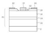
첨부된 도 1은 본 발명에 따른 Ⅲ-Ⅴ 화합물반도체를 이용한 FET의 일례인 HEMT의 단면 모식도이다. (이하, 본 발명에 따른 HEMT라 한다.)1 is a schematic cross-sectional view of HEMT, which is an example of a FET using a III-V compound semiconductor according to the present invention. (Hereinafter, referred to as HEMT according to the present invention.)
보이는 것처럼, 본 발명에 따른 HEMT는 기판(2) 상에 차례로 적층된 버퍼층(22), 채널층(24), 하이밴드갭층(26), 캡층(28)을 포함하는 Ⅲ-Ⅴ 화합물반도체 이종접합구조(20)와, Ⅲ-Ⅴ 화합물반도체 이종접합구조(20)의 캡층(28)에 오믹접촉된 소스 및 드레인영역(42,44) 그리고 소스 및 드레인영역(42,44) 사이의 게이트 리세스(32)를 통해 하이밴드갭층(28)과 쇼트키 접합된 금속게이트(50)를 포함한다.As can be seen, the HEMT according to the present invention is a III-V compound semiconductor heterojunction comprising a
각각을 자세히 살펴보면 다음과 같다.Looking at each of them in detail:
먼저, 기판(2)과 Ⅲ-Ⅴ 화합물반도체 이종접합구조(20)의 버퍼층(22), 채널층(24)은 일반적인 기술사상을 바탕으로 할 수 있다.First, the
즉, 기판(2)은 임의로 GaAs 등의 반절연성 물질로 이루어질 수 있고, 버퍼층(22)은 진성 GaAs 등의 Ⅲ-Ⅴ 화합물반도체 물질로 이루어질 수 있으며, 채널층(24)은 진성 AlGaAs 등의 Ⅲ-Ⅴ 화합물반도체 물질로 이루어질 수 있다. 참고로, 필요하다면 채널층(24)은 대역불연속을 위한 InGaAs와 AlGaAs 등의 이중 적층에 의한 슈도모르픽(pseudomorphic) 구조를 나타내는 것도 가능하며, 기판(2), Ⅲ-Ⅴ 화합물반도체 이종접합구조(20)의 버퍼층(22), 채널층(24)은 공지된 모든 재질이 사용될 수 있다.That is, the
다음으로 Ⅲ-Ⅴ 화합물반도체 이종접합구조(20)의 하이밴드갭층(26)은 Sb를 제외한 Ⅲ-Ⅴ 화합물반도체 물질로 이루어지고, 캡층(28)은 Sb를 포함한 Ⅲ-Ⅴ 화합물반도체 물질로 이루어진다. 그리고 하이밴드갭층(26)과 캡층(28)에는 각각 고농도 불순물이 도핑된다. Next, the high
즉, 본 발명에 따른 HEMT에 있어서 Ⅲ-Ⅴ 화합물반도체 이종접합구조(20)의 하이밴드갭층(26)은 고농도 도핑된 AlGaAs 등 Sb를 제외한 Ⅲ-Ⅴ 화합물반도체 물질로 제한되고, 캡층(28)은 GaSb 등 Sb를 포함한 Ⅲ-Ⅴ 화합물반도체 물질로 제한 되는 것을 특징으로 한다. 이는 후술하는 게이트 리세스 식각의 생략 또는 간소화를 위한 것으로서 해당 부분에서 상세히 살펴본다.That is, in the HEMT according to the present invention, the high
그리고 캡층(28)에는 서로 이격된 소스 및 드레인영역(42,44)이 오믹 접촉되고, 소스 및 드레인영역(42,44) 사이의 캡층(28)으로부터는 하이밴드갭층(26)을 일부 노출시키는 게이트 리세스(32)가 마련되어 해당 위치에서 금속게이트(50)와 하이밴드갭층(28)이 쇼트키 접합된다.The
한편, 첨부된 도 2는 본 발명의 변형예에 따른 HEMT의 단면모식도이다.On the other hand, Figure 2 is a schematic cross-sectional view of the HEMT according to a modification of the present invention.
앞서 도 1에서 살펴본 구성요소와 동일역할을 하는 동일부분에 대해서는 동일부호를 부여하였으므로 편의상 도 1과의 차이점만을 살펴보면, 본 발명의 변형예에 따른 HEMT는 Ⅲ-Ⅴ 화합물반도체 이종접합구조(20)의 하이밴드갭층(26)과 캡층(28) 사이로 5~30nm 두께를 나타내는 별도의 식각방지층(etch stop layer : 30)이 개재된다.Since the same reference numerals are given to the same parts that play the same role as the components described with reference to FIG. 1, the HEMT according to the modified example of the present invention is a III-V compound
이때, 식각방지층(30)은 Sb를 제외한 Ⅲ-Ⅴ 화합물반도체 물질, 일례로 InAs 등으로 제한되는 대신 하이밴드갭층(26)을 이루는 물질은 별도의 제한이 없다.In this case, the
즉, 본 발명은 Ⅲ-Ⅴ화합물반도체의 이종접합구조(20) 상의 게이트 리세스(32)를 필요로 하는 HEMT 등의 FET를 대상으로 하되, 특징적인 내용은 게이트 리세스(32)가 형성된 캡층(28)으로 Sb를 포함한 Ⅲ-Ⅴ 화합물반도체 물질을 사용하고, 그 하지층은 Sb를 제외한 Ⅲ-Ⅴ 화합물반도체 물질을 사용한다. That is, the present invention is directed to a FET such as a HEMT that requires a gate recess 32 on the
이로써 게이트 리세스(32)를 위한 별도의 식각 공정을 간소화한다.This simplifies a separate etching process for the
첨부된 도 3 내지 도 8은 각각 본 발명에 따른 Ⅲ-Ⅴ 화합물반도체를 이용한 FET의 공정단면도로서, 편의상 도 1에서 살펴본 HEMT에 대해 나타내었다. 도 1 및 도 2를 함께 참조한다.3 to 8 are each a process cross-sectional view of a FET using a III-V compound semiconductor according to the present invention, it is shown for the HEMT described in Figure 1 for convenience. Reference is made together to FIGS. 1 and 2.
먼저, 도 3에 도시된 것처럼 기판(2)을 준비한 후 선택적 결정성장을 통해 Ⅲ-Ⅴ 화합물반도체 이종접합구조(20)를 위한 버퍼층(22), 채널층(24), 하이밴드갭층(26), 캡층(28)을 구현한다.First, as shown in FIG. 3, after preparing the
이때, 선택적 결정성장은 공지 기술사상이 적용될 수 있고, 기판(2)은 임의로 GaAs와 같은 반절연성 물질로, 버퍼층(22)은 진성 GaAs와 같은 Ⅲ-Ⅴ 화합물반도체 물질로, 채널층(24)은 진성 AlGaAs와 같은 Ⅲ-Ⅴ 화합물반도체 물질로 각각 이루어질 수 있다. 그리고 하이밴드갭층(26)은 AlGaAs와 같이 Sb를 제외한 Ⅲ-Ⅴ 화합물반도체 물질로 이루어져 고농도로 도핑(n+)되고, 캡층(28)은 GaSb와 같이 Sb를 포함한 Ⅲ-Ⅴ 화합물반도체 물질로 이루어져 고농도 도핑(n+)된다. At this time, the selective crystal growth may be applied to a known technical idea, the
참고로, 필요하다면 하이밴드갭층(28)과 캡층(28) 사이로 InAs와 같이 Sb를 제외한 Ⅲ-Ⅴ 화합물반도체 물질로 이루어진 5~30nm 두께의 식각방지층(26)을 개재하는 것도 가능하며, 이 경우 하이밴드갭층(26)은 Sb를 제외한 Ⅲ-Ⅴ 화합물반도체 물질로 제한된 필요가 없음은 이미 도 2를 참조해서 살펴보았다.For reference, if necessary, it is possible to interpose a 5 to 30 nm thick
다음으로, 도 4에 도시된 것처럼 Ⅲ-Ⅴ 반도체화합물 이종접합구조(20)의 캡층(28)에 서로 이격된 소스 및 드레인영역(42,44)을 구현한다.Next, as shown in FIG. 4, source and drain
이때, 소스 및 드레인영역(42,44)은 금속박막의 증착, 포토리소그라피 또는 리프트 오프(lift-off), 식각에 의한 패터닝(patterning), 어닐링의 순서로 구현되 는데, 여기서 포토리소그라피란 목적하는 박막, 즉 금속층 위로 감광성 물질인 포토레지스트(photoresist)를 도포한 후 마스크(mask)로 노광(Exposure)하고 현상액으로 현상(deⅤelopment)하여 하지의 금속층을 선택적으로 노출시키는 포토레지스트패턴(photoresist pattern)을 얻는 과정을 총칭한다.In this case, the source and drain
그 결과 후속의 식각을 진행하면 캡층(28) 위에서 서로 이격된 소스 및 드레인영역(42,44)을 얻을 수 있고, 잔류 포토레지스트패턴을 제거한 후 어닐링을 진행하면 소스 및 드레인영역(42,44)이 완성된다.As a result, the source and drain
다음으로, 도 5에 도시된 것처럼 소스 및 드레인영역(42,44)과 그 사이로 노출된 캡층(28)을 덮도록 포토레지스트를 도포한다.Next, a photoresist is applied to cover the source and drain
이때, 포토레지스트는 빛을 받은 부분이 현상액에 의해 제거되는 포지티브 타입(positiⅤe)과 빛을 받지 않은 부분이 현상액에 의해 제거되는 네거티브(negatiⅤe) 타입으로 구분되지만 편의상 네거티브 타입이라 한다.In this case, the photoresist is classified into a positive type (positiVe) in which the lighted portion is removed by the developer and a negative type in which the non-lighted portion is removed by the developer, but is referred to as a negative type for convenience.
다음으로, 도 6에 도시된 것처럼 소스 및 드레인영역(42,44)과 캡층(28)을 덮는 포토레지스트막(60)에 마스크(70)를 대면 배치한 후 노광한다.Next, as shown in FIG. 6, the
이때, 마스크(70)는 빛을 차단하는 차단부(72)와 빛을 투과시키는 투과부(74)를 포함하며, 노광은 마스크(70)와 포토레지스트막(60)을 직접 접촉시키는 접촉방식(contact type), 마스크(70)와 포토레지스트막(60)을 일정 정도 이격시키는 근접방식(proximity type) 내지는 프로젝션 타입(projection type), 축소투영노광의 스탭 앤 리피트 방식(step and repeat type) 또는 스탭 앤 스캔 방식(step and scan type)이 가능하다.In this case, the
다음으로, 도 7에 도시된 바와 같이 소정의 현상액으로 현상한다.Next, as shown in FIG. 7, development is carried out with a predetermined developer.
이때, 본 발명은 현상액으로 TMAH(Tetra Methyl Ammonium Hydroxide) 수용액을 사용하며, TMAH 수용액은 바람직하게는 전체 중량 기준 97~99 중량%의 물과 전체 중량 기준 1~3중량%의 TMAH이 혼합된 형태를 나타낸다. 여기서 TMAH란 AZ300 등의 유기계열현상액에 함유되는 물질로서, 본 출원인의 실험과 연구를 통해 Sb를 포함하는 Ⅲ-Ⅴ 화합물반도체를 식각하는 특징이 있음을 알아내었다.In this case, the present invention uses a solution of Tetra Methyl Ammonium Hydroxide (TMAH) as a developer, and the TMAH solution is preferably a mixture of 97 to 99% by weight of water based on total weight and 1 to 3% by weight of TMAH based on total weight. Indicates. Here, TMAH is a substance contained in an organic-based developer such as AZ300, and it has been found through the experiments and studies of the applicant that there is a characteristic of etching the III-V compound semiconductor containing Sb.
그 결과 TMAH 수용액으로 포토레지스트막(도 6의 60 참조)을 현상하면 소스 및 드레인영역(42,44) 사이에 해당되는 일부가 제거된 포토레지스트패턴(62)이 얻어지는 동시에 포토레지스트패턴(62)에 의해 노출된 하지의 캡층(28) 일부가 함께 제거되어 게이트 리세스(62)가 얻어진다. 참고로, 본 출원인의 실험과 연구에 따르면 TMAH 수용액은 Sb를 포함하는 Ⅲ-Ⅴ 화합물반도체에 대해서만 선택적인 식각특성을 보이는 바, 캡층(28)과 달리 Sb를 제외한 Ⅲ-Ⅴ 화합물반도체 물질로 이루어진 하이밴드갭층(26)(또는 도 2의 식각방지층(30))에는 별다른 손상을 주지 않는다.As a result, when the photoresist film (see 60 in FIG. 6) is developed with a TMAH aqueous solution, a
하지만, 캡층(28)이 TMAH 수용액에 지나치게 장시간 노출되면 불필요한 측면손상 등이 발생할 수 있으므로 실온의 딥핑(dipping) 방식을 전제로 수 nm 범위의 캡층(28)에 대해 식각 시간은 20~30초가 적절하다.However, when the
다음으로, 도 8에 도시된 바와 같이 잔류의 포토레지스트패턴(도 7의 62 참조)을 제거하고, 게이트 리세스(32)에 금속게이트(50)를 형성하면 도 1에서 살펴본 본 발명에 따른 HEMT가 완성된다.Next, as shown in FIG. 8, if the remaining photoresist pattern (see 62 of FIG. 7) is removed, and the
이때, 금속게이트(50)를 위해서는 Ti, Au, Al 중 선택된 금속박막의 증착, 포토리소그라피, 식각에 의한 패터닝, 잔류 포토레지스트의 제거 등의 과정이 진행될 수 있다.In this case, for the
한편, 이상의 설명은 본 발명의 일례에 지나지 않는 것으로, 본 발명의 기술적 사상은 여기에 한정되지는 않는다. 즉, 본 발명은 Ⅲ-Ⅴ화합물반도체의 이종접합구조(20) 상의 게이트 리세스(32)를 필요로 하는 HEMT 등의 FET를 대상으로 하며, 게이트 리세스(32)를 위한 별도의 식각 공정을 생략 또는 간소화하기 위해 캡층(28)으로는 Sb를 포함하는 Ⅲ-Ⅴ 화합물반도체를 사용하고, 캡층(28) 위의 포토레지스트패턴을 위한 현상액으로는 TMAH 수용액을 사용한다. In addition, the above description is only an example of this invention, The technical idea of this invention is not limited to this. That is, the present invention is directed to FETs such as HEMT that require the
그 결과 본 발명의 적용범위와 구체적인 내용 등에서는 여러 가지 변형이 있을 수 있지만 이들 변형이 본 발명의 기술적 사상 내에 있다면 본 발명의 권리범위 내에 속한다 해야 할 것인바, 본 발명의 권리범위는 이하의 특허청구범위에 분명하게 명시되어 있다.As a result, there may be various modifications in the scope and details of the present invention, but if these modifications fall within the technical scope of the present invention, they should be included within the scope of the present invention. It is clearly stated in the claims.
도 1은 본 발명에 따른 Ⅲ-Ⅴ화합물반도체를 이용한 FET의 일례를 나타낸 단면 모식도.1 is a schematic cross-sectional view showing an example of a FET using a III-V compound semiconductor according to the present invention.
도 2는 본 발명에 따른 Ⅲ-Ⅴ화합물반도체를 이용한 FET의 변형예를 나타낸 단면 모식도.Figure 2 is a schematic cross-sectional view showing a modification of the FET using III-V compound semiconductor according to the present invention.
도 3 내지 도 8은 각각 본 발명에 따른 Ⅲ-Ⅴ화합물반도체를 이용한 FET의 일례에 대한 제조공정 단면도.3 to 8 are cross-sectional views of manufacturing processes for one example of a FET using a III-V compound semiconductor according to the present invention.
<도면의 주요 부분에 대한 부호의 설명><Explanation of symbols for the main parts of the drawings>
2 : 기판 20 : Ⅲ-Ⅴ 화합물반도체 이종접합구조2: substrate 20: III-V compound semiconductor heterojunction structure
22 : 버퍼층 24 : 채널층22: buffer layer 24: channel layer
26 : 하이밴드갭층 28 : 캡층26: high band gap layer 28: cap layer
30 : 식각방지층 32 : 게이트 리세스30: etch stop layer 32: gate recess
42,44 : 소스 및 드레인영역 50 : 금속게이트42, 44 Source and drain
60 : 포토레지스트막 62 : 포토레지스트패턴60
70 : 마스크70: mask
Claims (9)
Priority Applications (1)
| Application Number | Priority Date | Filing Date | Title |
|---|---|---|---|
| KR1020090016618A KR101098401B1 (en) | 2009-02-27 | 2009-02-27 | fabricating method of Field Effect Transistor using Ⅲ-Ⅴ compound semiconductor |
Applications Claiming Priority (1)
| Application Number | Priority Date | Filing Date | Title |
|---|---|---|---|
| KR1020090016618A KR101098401B1 (en) | 2009-02-27 | 2009-02-27 | fabricating method of Field Effect Transistor using Ⅲ-Ⅴ compound semiconductor |
Publications (2)
| Publication Number | Publication Date |
|---|---|
| KR20100097793A true KR20100097793A (en) | 2010-09-06 |
| KR101098401B1 KR101098401B1 (en) | 2011-12-26 |
Family
ID=43004839
Family Applications (1)
| Application Number | Title | Priority Date | Filing Date |
|---|---|---|---|
| KR1020090016618A Expired - Fee Related KR101098401B1 (en) | 2009-02-27 | 2009-02-27 | fabricating method of Field Effect Transistor using Ⅲ-Ⅴ compound semiconductor |
Country Status (1)
| Country | Link |
|---|---|
| KR (1) | KR101098401B1 (en) |
Cited By (3)
| Publication number | Priority date | Publication date | Assignee | Title |
|---|---|---|---|---|
| KR101256467B1 (en) * | 2012-02-06 | 2013-04-19 | 삼성전자주식회사 | Nitride baced heterostructure semiconductor device and manufacturing method thereof |
| US9076850B2 (en) | 2012-07-30 | 2015-07-07 | Samsung Electronics Co., Ltd. | High electron mobility transistor |
| KR20180079280A (en) * | 2012-12-17 | 2018-07-10 | 후지모리 고교 가부시키가이샤 | Adhesive layer and adhesive film |
-
2009
- 2009-02-27 KR KR1020090016618A patent/KR101098401B1/en not_active Expired - Fee Related
Cited By (3)
| Publication number | Priority date | Publication date | Assignee | Title |
|---|---|---|---|---|
| KR101256467B1 (en) * | 2012-02-06 | 2013-04-19 | 삼성전자주식회사 | Nitride baced heterostructure semiconductor device and manufacturing method thereof |
| US9076850B2 (en) | 2012-07-30 | 2015-07-07 | Samsung Electronics Co., Ltd. | High electron mobility transistor |
| KR20180079280A (en) * | 2012-12-17 | 2018-07-10 | 후지모리 고교 가부시키가이샤 | Adhesive layer and adhesive film |
Also Published As
| Publication number | Publication date |
|---|---|
| KR101098401B1 (en) | 2011-12-26 |
Similar Documents
| Publication | Publication Date | Title |
|---|---|---|
| US20160155801A1 (en) | Method of forming strained structures of semiconductor devices | |
| KR101805634B1 (en) | Semiconductor device comprising III-V group barrier and method of manufacturing the same | |
| KR100262940B1 (en) | Method for fabricating compound semiconductor device using lift-off of insulator | |
| KR100631051B1 (en) | Method of manufacturing amorphous high electron mobility transistor | |
| Czornomaz et al. | Scalability of ultra-thin-body and BOX InGaAs MOSFETs on silicon | |
| KR101098401B1 (en) | fabricating method of Field Effect Transistor using Ⅲ-Ⅴ compound semiconductor | |
| CN101027776A (en) | Enhancement - depletion field effect transistor structure and method of manufacture | |
| JP2014053418A (en) | Semiconductor device | |
| KR101020841B1 (en) | CMOS device and its manufacturing method | |
| JPH0864775A (en) | Method for manufacturing semiconductor device | |
| US9837417B1 (en) | Semiconductor device and method for fabricating the same | |
| TW201327816A (en) | Semiconductor device and method of manufacturing same | |
| US10083987B2 (en) | CMOS with middle of line processing of III-V material on mandrel | |
| JP3715557B2 (en) | Method for manufacturing field effect transistor | |
| US9583589B1 (en) | Self-aligned double gate recess for semiconductor field effect transistors | |
| JPH10107044A (en) | Manufacture of field effect transistor | |
| JPH10209177A (en) | Field effect transistor and method for forming gate electrode thereof | |
| JP2002141499A (en) | Field effect transistor and method of manufacturing the same | |
| JP3080215B2 (en) | Method for manufacturing field effect transistor | |
| KR100849926B1 (en) | Methods for fabricating a pseudomorphic high electron mobility transistor | |
| US10991814B2 (en) | Three-dimensional tunneling field-effect transistor and method of fabricating the same | |
| JP2607310B2 (en) | Method for manufacturing field effect transistor | |
| JP2004221245A (en) | Semiconductor device and manufacturing method thereof | |
| Egard et al. | Self-aligned gate-last surface channel In 0.53 Ga 0.47 As MOSFET with selectively regrown source and drain contact layers | |
| JPH06232168A (en) | Field effect transistor and method of manufacturing the same |
Legal Events
| Date | Code | Title | Description |
|---|---|---|---|
| A201 | Request for examination | ||
| PA0109 | Patent application |
St.27 status event code: A-0-1-A10-A12-nap-PA0109 |
|
| PA0201 | Request for examination |
St.27 status event code: A-1-2-D10-D11-exm-PA0201 |
|
| PN2301 | Change of applicant |
St.27 status event code: A-3-3-R10-R13-asn-PN2301 St.27 status event code: A-3-3-R10-R11-asn-PN2301 |
|
| R18-X000 | Changes to party contact information recorded |
St.27 status event code: A-3-3-R10-R18-oth-X000 |
|
| D13-X000 | Search requested |
St.27 status event code: A-1-2-D10-D13-srh-X000 |
|
| PG1501 | Laying open of application |
St.27 status event code: A-1-1-Q10-Q12-nap-PG1501 |
|
| D14-X000 | Search report completed |
St.27 status event code: A-1-2-D10-D14-srh-X000 |
|
| E902 | Notification of reason for refusal | ||
| PE0902 | Notice of grounds for rejection |
St.27 status event code: A-1-2-D10-D21-exm-PE0902 |
|
| T11-X000 | Administrative time limit extension requested |
St.27 status event code: U-3-3-T10-T11-oth-X000 |
|
| T11-X000 | Administrative time limit extension requested |
St.27 status event code: U-3-3-T10-T11-oth-X000 |
|
| T11-X000 | Administrative time limit extension requested |
St.27 status event code: U-3-3-T10-T11-oth-X000 |
|
| E13-X000 | Pre-grant limitation requested |
St.27 status event code: A-2-3-E10-E13-lim-X000 |
|
| P11-X000 | Amendment of application requested |
St.27 status event code: A-2-2-P10-P11-nap-X000 |
|
| P13-X000 | Application amended |
St.27 status event code: A-2-2-P10-P13-nap-X000 |
|
| E902 | Notification of reason for refusal | ||
| PE0902 | Notice of grounds for rejection |
St.27 status event code: A-1-2-D10-D21-exm-PE0902 |
|
| T11-X000 | Administrative time limit extension requested |
St.27 status event code: U-3-3-T10-T11-oth-X000 |
|
| E13-X000 | Pre-grant limitation requested |
St.27 status event code: A-2-3-E10-E13-lim-X000 |
|
| P11-X000 | Amendment of application requested |
St.27 status event code: A-2-2-P10-P11-nap-X000 |
|
| P13-X000 | Application amended |
St.27 status event code: A-2-2-P10-P13-nap-X000 |
|
| E701 | Decision to grant or registration of patent right | ||
| PE0701 | Decision of registration |
St.27 status event code: A-1-2-D10-D22-exm-PE0701 |
|
| GRNT | Written decision to grant | ||
| PR0701 | Registration of establishment |
St.27 status event code: A-2-4-F10-F11-exm-PR0701 |
|
| PR1002 | Payment of registration fee |
St.27 status event code: A-2-2-U10-U11-oth-PR1002 Fee payment year number: 1 |
|
| PG1601 | Publication of registration |
St.27 status event code: A-4-4-Q10-Q13-nap-PG1601 |
|
| R18-X000 | Changes to party contact information recorded |
St.27 status event code: A-5-5-R10-R18-oth-X000 |
|
| R18-X000 | Changes to party contact information recorded |
St.27 status event code: A-5-5-R10-R18-oth-X000 |
|
| PR1001 | Payment of annual fee |
St.27 status event code: A-4-4-U10-U11-oth-PR1001 Fee payment year number: 4 |
|
| FPAY | Annual fee payment |
Payment date: 20151030 Year of fee payment: 5 |
|
| PR1001 | Payment of annual fee |
St.27 status event code: A-4-4-U10-U11-oth-PR1001 Fee payment year number: 5 |
|
| LAPS | Lapse due to unpaid annual fee | ||
| PC1903 | Unpaid annual fee |
St.27 status event code: A-4-4-U10-U13-oth-PC1903 Not in force date: 20161220 Payment event data comment text: Termination Category : DEFAULT_OF_REGISTRATION_FEE |
|
| PC1903 | Unpaid annual fee |
St.27 status event code: N-4-6-H10-H13-oth-PC1903 Ip right cessation event data comment text: Termination Category : DEFAULT_OF_REGISTRATION_FEE Not in force date: 20161220 |
|
| R18-X000 | Changes to party contact information recorded |
St.27 status event code: A-5-5-R10-R18-oth-X000 |
|
| P22-X000 | Classification modified |
St.27 status event code: A-4-4-P10-P22-nap-X000 |