KR20100015225A - Liquid crystal display apparatus and touch sensing method thereof - Google Patents
Liquid crystal display apparatus and touch sensing method thereof Download PDFInfo
- Publication number
- KR20100015225A KR20100015225A KR1020080076172A KR20080076172A KR20100015225A KR 20100015225 A KR20100015225 A KR 20100015225A KR 1020080076172 A KR1020080076172 A KR 1020080076172A KR 20080076172 A KR20080076172 A KR 20080076172A KR 20100015225 A KR20100015225 A KR 20100015225A
- Authority
- KR
- South Korea
- Prior art keywords
- voltage
- calibration
- sensor
- sensed
- touch
- Prior art date
- Legal status (The legal status is an assumption and is not a legal conclusion. Google has not performed a legal analysis and makes no representation as to the accuracy of the status listed.)
- Ceased
Links
Images


Classifications
-
- G—PHYSICS
- G06—COMPUTING OR CALCULATING; COUNTING
- G06F—ELECTRIC DIGITAL DATA PROCESSING
- G06F3/00—Input arrangements for transferring data to be processed into a form capable of being handled by the computer; Output arrangements for transferring data from processing unit to output unit, e.g. interface arrangements
- G06F3/01—Input arrangements or combined input and output arrangements for interaction between user and computer
- G06F3/03—Arrangements for converting the position or the displacement of a member into a coded form
- G06F3/041—Digitisers, e.g. for touch screens or touch pads, characterised by the transducing means
- G06F3/0412—Digitisers structurally integrated in a display
-
- G—PHYSICS
- G02—OPTICS
- G02F—OPTICAL DEVICES OR ARRANGEMENTS FOR THE CONTROL OF LIGHT BY MODIFICATION OF THE OPTICAL PROPERTIES OF THE MEDIA OF THE ELEMENTS INVOLVED THEREIN; NON-LINEAR OPTICS; FREQUENCY-CHANGING OF LIGHT; OPTICAL LOGIC ELEMENTS; OPTICAL ANALOGUE/DIGITAL CONVERTERS
- G02F1/00—Devices or arrangements for the control of the intensity, colour, phase, polarisation or direction of light arriving from an independent light source, e.g. switching, gating or modulating; Non-linear optics
- G02F1/01—Devices or arrangements for the control of the intensity, colour, phase, polarisation or direction of light arriving from an independent light source, e.g. switching, gating or modulating; Non-linear optics for the control of the intensity, phase, polarisation or colour
- G02F1/13—Devices or arrangements for the control of the intensity, colour, phase, polarisation or direction of light arriving from an independent light source, e.g. switching, gating or modulating; Non-linear optics for the control of the intensity, phase, polarisation or colour based on liquid crystals, e.g. single liquid crystal display cells
- G02F1/133—Constructional arrangements; Operation of liquid crystal cells; Circuit arrangements
- G02F1/1333—Constructional arrangements; Manufacturing methods
- G02F1/13338—Input devices, e.g. touch panels
-
- G—PHYSICS
- G06—COMPUTING OR CALCULATING; COUNTING
- G06F—ELECTRIC DIGITAL DATA PROCESSING
- G06F3/00—Input arrangements for transferring data to be processed into a form capable of being handled by the computer; Output arrangements for transferring data from processing unit to output unit, e.g. interface arrangements
- G06F3/01—Input arrangements or combined input and output arrangements for interaction between user and computer
- G06F3/03—Arrangements for converting the position or the displacement of a member into a coded form
- G06F3/041—Digitisers, e.g. for touch screens or touch pads, characterised by the transducing means
- G06F3/0416—Control or interface arrangements specially adapted for digitisers
- G06F3/0418—Control or interface arrangements specially adapted for digitisers for error correction or compensation, e.g. based on parallax, calibration or alignment
-
- G—PHYSICS
- G06—COMPUTING OR CALCULATING; COUNTING
- G06F—ELECTRIC DIGITAL DATA PROCESSING
- G06F3/00—Input arrangements for transferring data to be processed into a form capable of being handled by the computer; Output arrangements for transferring data from processing unit to output unit, e.g. interface arrangements
- G06F3/01—Input arrangements or combined input and output arrangements for interaction between user and computer
- G06F3/03—Arrangements for converting the position or the displacement of a member into a coded form
- G06F3/041—Digitisers, e.g. for touch screens or touch pads, characterised by the transducing means
- G06F3/044—Digitisers, e.g. for touch screens or touch pads, characterised by the transducing means by capacitive means
Landscapes
- Engineering & Computer Science (AREA)
- General Engineering & Computer Science (AREA)
- Theoretical Computer Science (AREA)
- Physics & Mathematics (AREA)
- General Physics & Mathematics (AREA)
- Human Computer Interaction (AREA)
- Nonlinear Science (AREA)
- Chemical & Material Sciences (AREA)
- Crystallography & Structural Chemistry (AREA)
- Mathematical Physics (AREA)
- Optics & Photonics (AREA)
- Control Of Indicators Other Than Cathode Ray Tubes (AREA)
- Position Input By Displaying (AREA)
Abstract
본 발명의 액정 표시 장치는, 복수 개의 화소들과 복수 개의 센서들을 구비한 액정 패널, 그리고 상기 복수 개의 센서들 중 적어도 하나의 센서로부터 감지된 감지 전압과 상기 적어도 하나의 센서에 대응되는 기준 전압을 비교하여 상기 센서에 대한 터치 여부를 판별하는 터치 감지회로를 포함하며, 상기 기준 전압의 레벨은 상기 각각의 센서의 동작 특성을 고려하여 조정된다.The liquid crystal display of the present invention includes a liquid crystal panel having a plurality of pixels and a plurality of sensors, a sensing voltage sensed by at least one of the plurality of sensors, and a reference voltage corresponding to the at least one sensor. And a touch sensing circuit for determining whether to touch the sensor in comparison, wherein the level of the reference voltage is adjusted in consideration of operating characteristics of the respective sensors.
Description
본 발명은 액정 표시 장치에 관한 것으로, 좀 더 구체적으로는 액정 표시 장치의 터치 여부를 감지하는 장치 및 방법에 관한 것이다.The present invention relates to a liquid crystal display, and more particularly, to an apparatus and a method for detecting whether a liquid crystal display is touched.
최근 퍼스널 컴퓨터나 텔레비전 등의 경량화 및 박형화에 따라 표시 장치도 경량화 및 박형화가 요구되고 있으며, 이러한 요구에 따라 음극선관(cathode ray tube, CRT)이 평판 표시 장치(flat panel display)로 대체되고 있다.In recent years, with the reduction in weight and thickness of personal computers and televisions, display devices are also required to be lighter and thinner, and cathode ray tubes (CRTs) are being replaced by flat panel displays.
평판 표시 장치에는 액정 표시 장치(liquid crystal display, LCD), 전계 방출 표시 장치(field emission display, FED), 유기 발광 표시 장치(organic light emitting display), 플라스마 표시 장치(plasma display panel, PDP) 등이 포함된다. 그 중, 우수한 화질과, 경량, 박형, 저전력의 특징으로 인하여, 모바일(Mobile) 기기(예를 들면, 휴대용 컴퓨터, PDA(Personal Digital Assistants), 휴대 전화기 등)용 표시 장치로 액정 표시 장치(LCD) 장치가 가장 많이 사용되고 있다. 액정 표시 장치는, 화소 전극 및 공통 전극이 구비된 두 개의 투명 기판들(유리 기판)과, 상기 기판들 사이에 형성된 액정층을 포함한다. 액정 표시 장치는 액정층에 인가되는 전기장의 세기를 조절하여 액정층을 통과하는 빛의 투과율을 조절함으로써 원하는 화상을 얻는다.The flat panel display includes a liquid crystal display (LCD), a field emission display (FED), an organic light emitting display, a plasma display panel (PDP), and the like. Included. Among them, the liquid crystal display (LCD) is a display device for mobile devices (for example, portable computers, personal digital assistants (PDAs), cellular phones, etc.) due to excellent image quality, light weight, thinness, and low power. The device is the most used. The liquid crystal display includes two transparent substrates (glass substrates) including a pixel electrode and a common electrode, and a liquid crystal layer formed between the substrates. The liquid crystal display obtains a desired image by adjusting the intensity of the electric field applied to the liquid crystal layer to adjust the transmittance of light passing through the liquid crystal layer.
최근에는 액정 표시 장치와 같은 표시 장치들의 사용자 인터페이스의 용이성을 개선하기 위해, 터치 스크린 패널(Touch Screen Panel: TSP)의 개발이 활발히 이루어지고 있다. 터치 스크린 패널은 표시 장치의 화면 위에 사용자가 손가락 또는 터치 펜(touch pen, or stylus) 등을 접촉해 문자나 그림을 쓰고 그리거나, 아이콘을 실행시킴으로써, 컴퓨터 등과 같은 장치에서 원하는 명령이 수행되도록 하는 장치를 말한다. 그러나, 터치 스크린 패널이 부착된 액정 표시 장치는, 터치 스크린 패널의 추가로 인한 제조 원가 상승, 터치 스크린 패널을 액정 패널 위에 접착시키는 공정으로 인한 수율 감소, 액정 패널의 휘도 저하, 제품 두께 증가 등의 문제점들을 갖는다. Recently, in order to improve the ease of user interface of display devices such as liquid crystal displays, development of a touch screen panel (TSP) has been actively performed. The touch screen panel allows a user to perform a desired command on a device such as a computer by touching a finger or a touch pen (touch pen, or stylus) on the screen of the display device to write and draw letters or pictures, or to execute icons. Say the device. However, a liquid crystal display device with a touch screen panel includes a manufacturing cost increase due to the addition of the touch screen panel, a decrease in yield due to a process of bonding the touch screen panel onto the liquid crystal panel, a decrease in luminance of the liquid crystal panel, an increase in product thickness, and the like. Have problems.
이러한 문제점들을 해결하기 위해, 근래에는 액정 표시 장치에 터치 스크린 패널을 부착하는 대신, 센서(sensor)를 액정 표시 장치 내에 내장하는 기술이 개발되고 있다. 센서는 사용자의 손가락 등이 화면에 가한 빛 또는 압력의 변화 등을 감지함으로써, 사용자의 손가락 등이 액정 표시 장치의 화면에 터치(또는 접촉) 되었는지의 여부를 알아내는 데 이용된다.In order to solve these problems, in recent years, a technology for embedding a sensor in the liquid crystal display instead of attaching a touch screen panel to the liquid crystal display has been developed. The sensor is used to detect whether the user's finger or the like has touched (or touched) the screen of the liquid crystal display by detecting a change in light or pressure applied to the screen by the user's finger or the like.
본 발명의 목적은 액정 표시 장치에 내장된 센서들의 터치 유무를 정확하게 감지할 수 있는 장치 및 방법을 제공하는 데 있다.It is an object of the present invention to provide an apparatus and method capable of accurately detecting the presence or absence of touch of sensors embedded in a liquid crystal display.
본 발명의 다른 목적은 센서들의 터치 유무를 판단하는 데 사용되는 기준이되는 전압의 레벨을 자체적으로 조정(calibration)할 수 있는 장치 및 방법을 제공하는 데 있다.Another object of the present invention is to provide an apparatus and method capable of self-calibrating the level of a voltage, which is used as a reference for determining whether sensors are touched.
상기의 과제를 이루기 위하여 본 발명에 의한 액정 표시 장치는, 복수 개의 화소들과 복수 개의 센서들을 구비한 액정 패널; 그리고 상기 복수 개의 센서들 중 적어도 하나의 센서로부터 감지된 감지 전압과 상기 적어도 하나의 센서에 대응되는 기준 전압을 비교하여 상기 센서에 대한 터치 여부를 판별하는 터치 감지회로를 포함하며, 상기 기준 전압의 레벨은 상기 각각의 센서의 동작 특성을 고려하여 조정되는 것을 특징으로 한다.According to an aspect of the present invention, there is provided a liquid crystal display device including: a liquid crystal panel having a plurality of pixels and a plurality of sensors; And a touch sensing circuit comparing the sensed voltage sensed by at least one sensor among the plurality of sensors with a reference voltage corresponding to the at least one sensor to determine whether the touch is made on the sensor. The level is adjusted in consideration of the operating characteristics of each sensor.
이 실시예에 있어서, 상기 터치 감지회로는, 사용자 입력이 발생되는 노말 동작 이전에 적어도 한번 이상 상기 기준전압의 레벨을 조정하는 캘리브레이션 동작을 수행하는 것을 특징으로 한다.In this exemplary embodiment, the touch sensing circuit may perform a calibration operation of adjusting the level of the reference voltage at least once before a normal operation in which a user input is generated.
이 실시예에 있어서, 상기 캘리브레이션 동작은, 상기 센서들의 비-터치 이벤트시 감지된 전압을 이용하여 수행되는 것을 특징으로 한다.In this embodiment, the calibration operation is performed by using a voltage sensed at the non-touch event of the sensors.
이 실시예에 있어서, 상기 터치 감지회로는, 상기 캘리브레이션 동작시 상기 비-터치 이벤트시 감지된 전압을 상기 기준전압으로 발생하는 것을 특징으로 한다.In this exemplary embodiment, the touch sensing circuit may generate a voltage sensed as the reference voltage during the non-touch event during the calibration operation.
이 실시예에 있어서, 상기 터치 감지회로는, 상기 캘리브레이션 동작시 상기 비-터치 이벤트시 감지된 전압을 소정 레벨 증가 내지 감소시키고, 상기 증가 내지 감소된 전압을 상기 기준전압으로 발생하는 것을 특징으로 한다.In this embodiment, the touch sensing circuit is characterized in that during the calibration operation, the voltage detected during the non-touch event increases or decreases by a predetermined level and generates the increased or decreased voltage as the reference voltage. .
이 실시예에 있어서, 상기 비-터치 이벤트시 감지된 전압의 레벨은, 상기 터치 감지 회로의 내부 저항열의 분배율 및 동작전압의 레벨을 변경함에 의해 증가 내지 감소되는 것을 특징으로 한다.In this embodiment, the level of the voltage sensed during the non-touch event is increased or decreased by changing the distribution ratio of the internal resistance heat of the touch sensing circuit and the level of the operating voltage.
상기의 과제를 이루기 위하여 본 발명에 의한 액정 표시 장치는, 복수 개의 화소들과 복수 개의 센서들을 구비한 액정 패널; 상기 화소들에 표시될 영상 신호에 대응되는 데이터 전압을 발생하는 구동부; 상기 복수 개의 센서들 중 적어도 하나의 센서로부터 감지된 감지 전압과 상기 적어도 하나의 센서에 대응되는 기준 전압을 비교하여 상기 센서에 대한 터치 여부를 판별하는 터치 감지회로; 그리고 상기 구동부 및 상기 터치 감지회로의 동작을 제어하는 타이밍 제어부를 포함하며, 상기 기준 전압의 레벨은 상기 각각의 센서의 동작 특성을 고려하여 조정되는 것을 특징으로 한다.According to an aspect of the present invention, there is provided a liquid crystal display device including: a liquid crystal panel having a plurality of pixels and a plurality of sensors; A driver configured to generate a data voltage corresponding to an image signal to be displayed on the pixels; A touch sensing circuit configured to compare whether the sensing voltage sensed by at least one sensor among the plurality of sensors and a reference voltage corresponding to the at least one sensor determines whether to touch the sensor; And a timing controller for controlling the operation of the driver and the touch sensing circuit, wherein the level of the reference voltage is adjusted in consideration of operating characteristics of the respective sensors.
이 실시예에 있어서, 상기 터치 감지 회로는 상기 구동부 및 상기 타이밍 제어부 중 하나에 구비되는 것을 특징으로 한다.In this embodiment, the touch sensing circuit may be provided in one of the driver and the timing controller.
이 실시예에 있어서, 상기 터치 감지회로는 상기 센서들 각각으로부터 발생된 감지 전류로부터 상기 감지 전압을 발생하는 적분부; 캘리브레이션 동작시 상기 적분부에서 발생된 상기 감지 전압으로부터 상기 센서들 각각에 대응되는 캘리브레이션 전압을 발생하고, 노말 동작시 상기 캘리브레이션 전압을 상기 기준전압으로 제공하는 캘리브레이션부; 그리고 노말 동작시 상기 적분부에서 발생된 상기 감지 전압과 상기 기준 전압을 비교하여 상기 센서의 터치 유무를 판단하는 비교부를 포함하는 것을 특징으로 한다.In this embodiment, the touch sensing circuit includes an integrating unit for generating the sensing voltage from the sensing current generated from each of the sensors; A calibration unit configured to generate a calibration voltage corresponding to each of the sensors from the sensed voltage generated by the integrator during a calibration operation, and to provide the calibration voltage as the reference voltage during a normal operation; And comparing the sensing voltage generated by the integrating unit with the reference voltage during normal operation to determine whether the sensor is touched.
이 실시예에 있어서, 상기 캘리브레이션부는 상기 캘리브레이션 동작시 상기 적분부로부터 발생된 상기 감지 전압을 디지털 형태로 변환하는 아날로그-디지털 변환기; 상기 디지털 형태로 변환된 상기 감지 전압을 저장하는 메모리; 그리고 상기 메모리에 저장된 상기 감지 전압을 아날로그 형태로 변환하여 상기 캘리브레이션 전압을 발생하는 디지털-아날로그 변환기를 포함하며, 상기 캘리브레이션 전압의 레벨은 상기 디지털-아날로그 변환기에 구비된 저항들의 분배비 및 동작 전압 중 적어도 하나를 이용하여 조정되는 것을 특징으로 한다.In this embodiment, the calibration unit comprises: an analog-to-digital converter for converting the sensed voltage generated from the integrating unit into a digital form during the calibration operation; A memory for storing the sensed voltage converted into the digital form; And a digital-to-analog converter that converts the sensed voltage stored in the memory into an analog form to generate the calibration voltage, wherein the level of the calibration voltage is at least one of a distribution ratio and an operating voltage of resistors included in the digital-to-analog converter. It is characterized by being adjusted using one.
이 실시예에 있어서, 상기 캘리브레이션부는 상기 메모리에 저장된 상기 감지 전압의 각각의 비트를 순차적으로 래치하고, 상기 래치된 상기 각각의 비트를 동시에 상기 디지털-아날로그 변환기로 제공하는 래치; 그리고 상기 디지털-아날로그 변환기의 출력을 상기 비교부로 제공하는 출력 버퍼를 더 포함하는 것을 특징으로 한다.In this embodiment, the calibration unit comprises: a latch sequentially latching each bit of the sense voltage stored in the memory, and simultaneously providing the latched bit to the digital-analog converter; And an output buffer for providing the output of the digital-analog converter to the comparator.
이 실시예에 있어서, 상기 동작 전압을 생성 내지 조정하는 전압 생성부를 더 포함하는 것을 특징으로 한다.In this embodiment, further comprising a voltage generator for generating or adjusting the operating voltage.
이 실시예에 있어서, 상기 노말 동작이 수행되기 이전에 적어도 한 번 이상 상기 캘리브레이션 동작이 수행되는 것을 특징으로 한다.In this embodiment, the calibration operation is performed at least once before the normal operation is performed.
이 실시예에 있어서, 상기 캘리브레이션 전압은 비-터치 이벤트시 상기 센서들 각각으로부터 감지된 전압인 것을 특징으로 한다.In this embodiment, the calibration voltage is characterized in that the voltage sensed from each of the sensors in the non-touch event.
이 실시예에 있어서, 상기 캘리브레이션 전압은 비-터치 이벤트시 상기 센서들 각각으로부터 감지된 전압을 소정 레벨 증가 내지 감소시킨 전압인 것을 특징으 로 한다.In this embodiment, the calibration voltage is characterized in that the voltage detected by each of the sensors in the non-touch event increases or decreases a predetermined level.
이 실시예에 있어서, 상기 비-터치 이벤트시 감지된 전압의 레벨은, 내부 저항열의 분배율 및 동작전압의 레벨을 변경함에 의해 증가 내지 감소되는 것을 특징으로 한다.In this embodiment, the level of the voltage sensed during the non-touch event is increased or decreased by changing the distribution ratio of the internal resistance heat and the level of the operating voltage.
상기의 과제를 이루기 위하여 복수 개의 화소들과 복수 개의 센서들을 구비한 본 발명의 액정 패널의 터치 감지 방법은, 캘리브레이션 동작시 비 터치 이벤트에 대응되는 상기 복수 개의 센서들 각각의 전압 특성을 고려하여 상기 각각의 센서에 대응되는 캘리브레이션 전압을 발생하는 단계; 노말 동작시 상기 복수 개의 센서들 중 적어도 어느 하나로부터 감지 전압을 받아들이는 단계; 상기 감지 전압과 상기 적어도 어느 하나의 센서에 대응되는 캘리브레이션 전압을 비교하는 단계; 그리고 상기 비교 결과를 근거로 하여 상기 적어도 어느 하나의 센서의 터치 여부를 판별하는 단계를 포함하는 것을 특징으로 한다.In order to achieve the above object, in the touch sensing method of the liquid crystal panel according to the present invention having a plurality of pixels and a plurality of sensors, the voltage characteristics of each of the plurality of sensors corresponding to the non-touch event during the calibration operation may be determined. Generating a calibration voltage corresponding to each sensor; Accepting a sensed voltage from at least one of the plurality of sensors during normal operation; Comparing the sensing voltage with a calibration voltage corresponding to the at least one sensor; And determining whether the at least one sensor is touched based on the comparison result.
이 실시예에 있어서, 상기 캘리브레이션 전압을 발생하는 단계는, 상기 액정 패널에 구비된 센서들 각각에 대해 수행되는 것을 특징으로 한다.In this embodiment, the generating of the calibration voltage may be performed for each of the sensors provided in the liquid crystal panel.
이 실시예에 있어서, 상기 노말 동작이 수행되기 이전에 적어도 한 번 이상 상기 캘리브레이션 동작이 수행되는것을 특징으로 한다.In this embodiment, the calibration operation is performed at least once before the normal operation is performed.
이 실시예에 있어서, 상기 캘리브레이션 전압을 발생하는 단계는 상기 각각의 센서로부터 감지된 감지 전압을 디지털 형태로 변환하는 단계; 상기 디지털 형태로 변환된 상기 감지 전압을 메모리에 저장하는 단계; 그리고 상기 메모리에 저장된 상기 감지 전압을 아날로그 형태로 변환하여 상기 캘리브레이션 전압을 발생 하는 단계를 포함하며, 상기 캘리브레이션 전압의 레벨은 상기 각각의 센서로부터 감지된 감지 전압과 소정의 전압차를 갖도록 조정되는 것을 특징으로 한다.In this embodiment, the generating of the calibration voltage may include converting a sensed voltage sensed by each sensor into a digital form; Storing the sensed voltage converted into the digital form in a memory; And generating the calibration voltage by converting the sense voltage stored in the memory into an analog form, wherein the level of the calibration voltage is adjusted to have a predetermined voltage difference with the sense voltage sensed by the respective sensors. It features.
이상과 같은 본 발명에 의하면, 액정 표시 장치에 내장된 센서들 각각의 동작 특성에 대응되도록 기준 전압의 레벨을 자체적으로 조정할 수 있게 된다. 그 결과, 공정 변화 등의 여러 요인으로 인해 센서들의 특성이 달라지더라도 센서들의 터치 여부를 정확하게 감지할 수 있게 된다.According to the present invention as described above, the level of the reference voltage can be adjusted by itself so as to correspond to the operating characteristics of each of the sensors embedded in the liquid crystal display. As a result, even if the characteristics of the sensors are changed due to various factors such as process change, it is possible to accurately detect whether the sensors are touched.
이하 본 발명의 액정 표시 장치 및 그것의 터치 감지 방법이 첨부된 도면을 참조하여 상세히 설명될 것이다. 이는 본 발명의 예시적인 실시예로서, 본 발명의 기술적 사상을 벗어나지 않는 범위 내에서 다양한 변화 및 변경이 가능함은 물론이다. Hereinafter, a liquid crystal display and a touch sensing method thereof according to the present invention will be described in detail with reference to the accompanying drawings. This is an exemplary embodiment of the present invention, of course, various changes and modifications are possible without departing from the spirit of the present invention.
본 발명의 신규한 액정 표시 장치는 복수 개의 화소들과 복수 개의 센서들로 구성된 액정 패널을 포함한다. 본 발명의 신규한 액정 표시 장치는 캘리브레이션 구간 동안 터치 감지 회로를 통해 센서들로부터 전류를 감지하고, 감지된 전류에 대응되는 감지 전압을 메모리에 저장한다. 캘리브레이션 구간은 터치가 발생되지 않는 소정의 구간을 의미하고, 캘리브레이션 구간 동안 감지된 전압은 터치가 발생되지 않았을 경우에 센서로부터 감지된 감지 전압을 의미한다. 본 발명의 터치 감지 회로는 캘리브레이션 구간 동안 메모리에 저장된 감지 전압들에 대해 레벨을 자체적으로 조정(self-calibration)하고, 전압 조정 결과로서 캘리브레이션 전압을 발생한다. 캘리브레이션 전압은 노말 동작시 감지된 감지 전압과 비교되어, 센서의 터치 여부를 판단하는 데 사용된다. 캘리브레이션 전압은 각각의 센서의 터치 여부를 판단하는 기준전압으로 사용된다. 캘리브레이션 전압은 특정 레벨로 고정되지 않고, 액정 표시 장치에 내장된 센서들 각각의 동작 특성에 대응되도록 가변 된다. 본 발명에 따른 액정 표시 장치 및 그것의 터치 감지 회로에 대한 상세 구성은 다음과 같다. The novel liquid crystal display of the present invention includes a liquid crystal panel composed of a plurality of pixels and a plurality of sensors. The novel liquid crystal display of the present invention senses current from the sensors through the touch sensing circuit during the calibration period, and stores a sensing voltage corresponding to the sensed current in the memory. The calibration section refers to a predetermined section in which no touch is generated, and the voltage sensed during the calibration section refers to a sensing voltage sensed by the sensor when no touch is generated. The touch sensing circuit of the present invention self-calibrates the levels with respect to the sense voltages stored in the memory during the calibration period and generates the calibration voltage as a result of the voltage adjustment. The calibration voltage is compared with the sensed voltage detected during normal operation and used to determine whether the sensor is touched. The calibration voltage is used as a reference voltage for determining whether each sensor is touched. The calibration voltage is not fixed to a specific level, and is varied to correspond to operating characteristics of each of the sensors built in the liquid crystal display. The detailed configuration of the liquid crystal display device and its touch sensing circuit according to the present invention is as follows.
도 1은 본 발명이 적용되는 액정 패널(110)의 구성을 보여주는 블록도이다. 그리고, 도 2는 도 1에 도시된 화소(101) 및 센서(102)의 등가회로와, 본 발명의 실시예에 따른 터치 감지회로(500)의 구성을 보여주는 도면이다. 1 is a block diagram showing the configuration of a
아래에서 상세히 설명되겠지만, 도 1 및 도 2에 도시된 액정 패널(110)은 터치 스크린 패널과 액정 패널이 일체화된 패널, 또는 터치 스크린 기능이 내장된 액정 패널을 의미한다. 도 1 및 도 2에 도시된 액정 패널(110)의 구성은, 본 발명이 적용되는 액정 패널의 구성을 예시적으로 보여주는 도면으로서, 액정 패널(110)의 구성 요소들(예를 들면, 화소 및 센서)과, 그것들의 형성 방법, 배선, 연결 관계 등은 다양한 형태로 구성 가능하다. As will be described in detail below, the
도 1을 참조하면, 액정 패널(110)은 일 방향으로 연장된 복수의 게이트 라인들(G1 내지 Gn)을 구비한다. 액정 패널(110)은 상기 게이트 라인들(G1 내지 Gn)과 교차하는 방향으로 배선된 복수의 데이터 라인들(D1 내지 Dm) 및 복수의 센서 라인들(TL1 내지 TLj)을 구비한다. 액정 패널(110)은 도 2에 도시된 바와 같이 게이트 라인들(G1 내지 Gn)과 동일 방향으로 연장된 복수의 센싱 전압 공급 라인(Vcs)을 더 구비할 수 있다. Referring to FIG. 1, the
게이트 라인들(G1 내지 Gn)과 데이터 라인들(D1 내지 Dm)의 교차 영역에는 복수의 화소들(101; 101-R, 101-G, 101-B)이 접속된다. 그리고, 게이트 라인들(G1 내지 Gn)과 센서 라인들(TL1 내지 TLj)의 교차 영역에는 복수의 센서들(102)이 접속된다. 복수의 화소들(101)과 복수의 센서들(102)은 액정 패널(110)의 표시 영역 내에 매트릭스 형태로 배열된다. A plurality of pixels 101 (101-R, 101-G, and 101-B) are connected to an intersection area between the gate lines G1 to Gn and the data lines D1 to Dm. In addition, a plurality of
하나의 화소(101)는, 적색 화소(101-R), 녹색 화소(101-G), 청색 화소(101-B)로 구성될 수 있으며, 하나의 화소(101)에는 하나의 센서(102)가 할당될 수 있다. 이때, 적색 화소(101-R), 녹색 화소(101-G), 청색 화소(101-B), 및 센서(102)는 하나의 표시 그룹으로 정의될 수 있다. 하나의 표시 그룹을 형성하는 적색 화소(101-R), 녹색 화소(101-G), 청색 화소(101-B), 및 센서(102)는 행 방향으로 연속 배치될 수 있다. 적색 화소(101-R), 녹색 화소(101-G), 및 청색 화소(101-B)는 각각 대응되는 데이터 라인(D1 내지 D3)에 접속되고, 센서(102)는 대응되는 센서 라인(TL1)에 각각 접속된다. 즉, 3개의 데이터 라인마다 하나의 센서 라인이 배치될 수 있다. 하지만, 도 1에 도시된 표시 그룹의 구성 및 배열 형태는 본 발명이 적용되는 일 예에 불과하며, 각각의 표시 그룹을 구성하는 화소들 및 센서의 구성은 다양한 형태로 정의될 수 있다. 또한, 각각의 표시 그룹의 구성 형태에 따라서 대응되는 데이터 라인들 및 센서 라인들의 배선 형태 또한 다양하게 구성될 수 있다.One
도 2를 참조하면, 각각의 화소(101 ; 101-R, 101-G,101-B)는 박막 트랜지스 터(TFT; Thin Film Transistor)(T) 및 액정 커패시터(Clc)를 포함한다. 각각의 화소(101 ; 101-R, 101-G,101-B)는 유지 커패시터(Cst)를 더 포함할 수 있다. 박막 트랜지스터(T)의 게이트 단자는 대응되는 게이트 라인(Gj)에 접속되고, 소스 단자는 대응되는 데이터 라인(Dk)에 접속된다. 박막 트랜지스터(T)의 드레인 단자는 액정 커패시터(Clc)와 유지 커패시터(Cst) 각각의 일 단자에 접속될 수 있다. Referring to FIG. 2, each pixel 101 (101-R, 101-G, 101-B) includes a thin film transistor (TFT) and a liquid crystal capacitor Clc. Each pixel 101 (101-R, 101-G, 101-B) may further include a holding capacitor Cst. The gate terminal of the thin film transistor T is connected to the corresponding gate line Gj, and the source terminal is connected to the corresponding data line Dk. The drain terminal of the thin film transistor T may be connected to one terminal of each of the liquid crystal capacitor Clc and the storage capacitor Cst.
제 1 스위치(S1)는 대응되는 터치라인(TLi)과 센싱 전압 공급 라인(Vcs) 사이에 접속된다. 제 2 스위치(S2)는 대응되는 게이트 라인(Gj-1)과 제 1 노드(N) 사이에 접속된다. 여기서, 제 1 스위치(S1)는 제 1 노드(N)의 전압에 따라 온/오프 된다. 제 2 스위치(S2)는 뒷단의 게이트 라인(Gj)에 의해 온/오프된다. 기준 커패시터(Cr)는 해당 게이트 라인(Gj-1)과 제 1 노드(N)에 접속된다. 센서 커패시터(Cts)의 일 단자는 제 1 노드(N)에 접속되고, 타 단자는 공통 전압(Vcom)을 인가 받는다. 센서 커패시터(Cts)는 커패시턴스 값이 변화하는 가변 커패시터로 구성될 수 있다. 제 1 및 제 2 스위치(S1, S2)로 박막 트랜지스터를 사용하는 것이 바람직하다. The first switch S1 is connected between the corresponding touch line TLi and the sensing voltage supply line Vcs. The second switch S2 is connected between the corresponding gate line Gj-1 and the first node N. FIG. Here, the first switch S1 is turned on / off according to the voltage of the first node N. The second switch S2 is turned on / off by the rear gate line Gj. The reference capacitor Cr is connected to the corresponding gate line Gj-1 and the first node N. One terminal of the sensor capacitor Cts is connected to the first node N, and the other terminal receives a common voltage Vcom. The sensor capacitor Cts may be configured as a variable capacitor whose capacitance value changes. It is preferable to use a thin film transistor as the first and second switches S1 and S2.
센서(102)에 사용자의 손가락 등이 터치되면, 센서(102)와 접속된 센서 라인(TLi)에는 전류의 변화가 발생하게 된다. 센서 라인(TLi)을 통해 흐르는 전류를 감지 전류(Isense)라 한다. 감지 전류(Isense)는 아래의 [수학식 1]과 같이 모델링될 수 있다.When the user's finger or the like touches the
여기서, CSiNx는 센서(102)를 구성하는 커패시터들의 절연막 성분(예를 들면, SiNx)에 따른 커패시턴스 값을 의미한다. 그리고, Vth는 센서(102)를 구성하는 박막 트랜지스터의 문턱전압을 의미하고, VGS는 상기 박막 트랜지스터의 게이트-소오스 전압을 의미한다. Here, C SiNx refers to a capacitance value according to the insulating film component (eg, SiNx) of the capacitors constituting the
터치(touch) 또는 비-터치(un-touch)의 이벤트가 센서(102)에 인가되면, 센서(102)를 구성하는 박막 트랜지스터의 게이트-소오스 전압(VGS)이 변화하게 된다. 변화된 박막 트랜지스터의 게이트-소오스 전압(VGS)은 감지 전류(Isense)를 변화시킨다. When a touch or non-touch event is applied to the
터치 감지 회로(touch sensing circuit ; 500)는 감지 전류(Isense)를 받아들여 센서(102)의 터치 유/무를 판별한다. 아래에서 상세히 설명되겠지만, 본 발명의 터치 감지 회로(500)는 센서(102)의 터치 유/무를 판별함에 있어서, 고정된 레벨의 기준전압을 사용하지 않고, 센서(102)마다 레벨이 자체적으로 조정된 캘리브레이션 전압(VCALI)을 기준전압으로 사용한다. 캘리브레이션 전압(VCALI)은 각 센서(102)의 동작 특성(특히, 각 센서(102)가 가지고 있는 터치/비-터치 이벤트의 전압 특성)을 근거로 하여 발생된다. 캘리브레이션 전압(VCALI)을 발생하기 위해, 본 발명의 터치 감지 회로(500)는 적분부(integration unit ; 510), 캘리브레이션 부(calibration unit ; 530), 및 비교부(comparison unit ; 550)를 포함한다. The
적분부(510)는 감지 전류(Isense)를 더하여 감지 전압(Vsense)을 발생하는 기능을 수행한다. 감지 전압(Vsense)은 아래의 [수학식 2]와 같이 모델링 될 수 있다.The
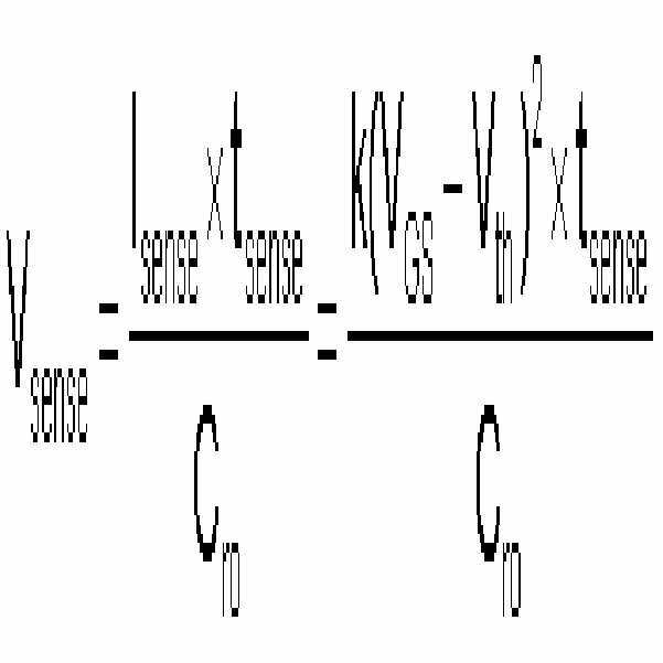
여기서, k=0.5*u*C*W/L로 정의될 수 있다. Cro은 적분부(510)의 커패시턴스 값(capacitance value)을 의미하고, tsense 감지 시간을 의미한다. Here, k may be defined as 0.5 * u * C * W / L. Cro means a capacitance value of the integrating
액정 기판(110)이 점점 대형화됨에 따라, 대형 유리 기판의 공정상 아래와 같은 불균일성(non-uniformity) 문제가 발생할 수 있다. 예를 들어, 센서(102) 회로 내의 박막 트랜지스터의 문턱전압(Vth), 이동도(mobility), 커패시턴스(CSiNx)가 불균일하게 구성될 수 있다. 이 경우, 센서(102) 회로에 의해 동일한 게이트-소오스 전압(VGS)이 결정된다 하더라도, 감지 전류(Isense)에 변화가 생기게 된다. 특히, 박막 트랜지스터의 문턱전압(Vth)은 a-Si 박막 트랜지스터의 전기적 열화 특성 때문에 장시간 동작시키게 되면 그 레벨이 쉬프트(shift)하게 된다. 또한, 각 센서(102) 회로 내의 셀 갭(cell gap)이 불균일하게 형성되는 경우, 박막 트랜지스터의 게이트-소오스 전압(VGS)이 변화될 수 있다. 예를 들면, 대형 유리 기판 내에서 셀의 갭(cell gap)은, 패널 대 패널(panel to panel), 셀 대 셀(cell to cell)마다 불균일하게 구성될 수 있다(약 30%). 셀 갭이 불균일하게 되면, 센서(102) 회로 내부의 액정 커패시턴스(capacitance)가 불균일하게 되고, 결국은 박막 트랜지스터의 게이트-소오스 전압(VGS)이 변화하게 된다. 따라서, 동일한 박막 트랜지스터의 문턱전압(Vth)이 유리기판에 형성된다 하더라도, 센서(102)의 터치와 무관하게 감지 전류(Isense)가 변화하게 된다. 이 외에도, 각 센서(102) 회로를 읽는 감지 시간(sensing time)이 변화됨으로써 감지 전류(Isense)가 변화되기도 한다.As the
이상과 같은 액정 기판(110)의 공정상의 특성과 그로 인한 감지 전류(Isense)의 변화는, 본 발명에서 센서(102)의 터치 여부의 판단시 중요한 요소로서 고려된다. 즉, 본 발명에서는 각각의 센서(102)의 전압 특성에 따라 전압 레벨이 자체적으로 조정(self-calibration)된 캘리브레이션 전압(VCALI)을 발생하고, 이를 기준전압으로 이용하여 센서(102)의 터치 유무를 판별한다. 그 결과, 센서(102) 오감지 문제를 방지할 수 있고, 센서(102)의 감지 특성을 향상시킬 수 있게 된다. The above-described process characteristics of the
본 발명의 터치 감지 회로(500)는 두 개의 동작 모드를 갖는다. 하나는 노말 모드(normal mode)이고, 다른 하나는 캘리브레이션 모드(calibration mode)이다. 캘리브레이션 모드는, 비-터치 시의 센서(102)의 동작 특성을 반영하여 캘리브레이션 전압(VCALI)을 발생하는 동작 모드이다. 캘리브레이션 전압(VCALI)은, 캘리브레이션 구간 동안 캘리브레이션부(530)에서 발생된다. 캘리브레이션 모드는, 기본적으로 액정 패널(110)에 비-터치 이벤트가 발생되는 구간으로 정의될 수 있다. 예를 들면, 캘리브레이션 모드는 액정 패널(110)이 턴-온(turn on)되었을 때, 노말 동작 이 수행되고 난 후 n 프레임이 경과 되었을 때(n은 1 이상의 정수), 사용자 선택 모드 등으로 다양하게 정의될 수 있고, 타이머 등을 이용하여 설정될 수도 있다. The
노말 모드는 사용자 입력이 발생되는 정상 동작 구간을 의미한다. 노말 모드 구간에서는, 센서(102)로부터 감지된 감지 전압(Vsense)과, 캘리브레이션 전압(VCALI)을 비교하여, 센서(102)의 터치 여부를 판단한다. 감지 전압(Vsense)과 캘리브레이션 전압(VCALI)의 비교는 노말 구간 동안 비교부(550)에서 수행된다. 정확한 비교를 수행하기 위해서는, 노말 구간이 시작되기 이전에 적어도 한 번 이상의 캘리브레이션 모드가 수행됨이 바람직하다. 따라서, 액정 표시장치(100)의 파워 온 시점에서 캘리브레이션 동작이 자체적으로 수행되도록 구현할 수도 있다. The normal mode refers to a normal operation section in which user input is generated. In the normal mode section, it is determined whether the
비교부(550)는 상기 비교 결과에 따라서, 터치 신호(TCH) 또는 비-터치 신호(NOTCH)를 발생한다. 예를 들어, 상기 비교 결과, 감지 전압(Vsense)과 캘리브레이션 전압(VCALI) 사이에 전압 차가 존재하면, 비교부(550)는 선택된 센서(102)에서는 터치 이벤트가 발생된 것으로 판단하고, 터치 신호(TCH)를 발생한다. 그리고, 감지 전압(Vsense)과 캘리브레이션 전압(VCALI) 사이에 전압 차가 존재하지 않으면, 비교부(550)는 선택된 센서(102)에서는 터치 이벤트가 발생되지 않은 것으로(즉, 비-터치 이벤트로) 판단하고, 비-터치 신호(NOTCH)를 발생한다. 비교부(550)로부터 발생된 터치 신호(TCH)/비-터치 신호(NOTCH)는 사용자로부터 입력된 명령을 인식하는데 사용된다.The
캘리브레이션 모드 및 노말 모드에서의, 감지 전압(Vsense) 및 캘리브레이션 전압(VCALI)의 제공 경로는, 터치 감지 회로(500)에 구비된 제 1 내지 제 3 스위치들(S11-S13)의 스위칭 동작에 의해 제어된다. 제 1 및 제 3 스위치(S11, S13)의 스위칭 동작은 SNI(Sending Normal Information) 신호에 의해 제어된다. 제 2 스위치(S12)의 스위칭 동작은 SCI(Sending Calibration Information) 신호에 의해 제어된다. 아래에서 상세히 설명되겠지만, SCI 신호 및 SNI 신호의 활성화/비활성화되는 시점은 터치 감지 회로(500) 외부의 제어 로직(예를 들면, 타이밍 제어부(timing control unit))에 의해 제어될 수 있다.In the calibration mode and the normal mode, the providing path of the sensing voltage Vsense and the calibration voltage V CALI may be applied to the switching operation of the first to third switches S11 to S13 included in the
앞에서 설명된 캘리브레이션 전압(VCALI)의 발생 기능(즉, 기준전압의 자체조정 기능)은, 각 센서(102)가 가지고 있는 터치/비-터치 이벤트(특히, 비-터치 이벤트)에 대한 전압 특성을 근거로 하여 수행된다. 각 센서(102)가 가지고 있는 터치/비-터치 이벤트에 대한 전압 특성을 살펴보면 다음과 같다. The generation function of the calibration voltage V CALI described above (i.e., self-adjustment of the reference voltage) is a voltage characteristic for touch / non-touch events (especially non-touch events) that each
도 3 및 도 4는 도 1에 도시된 센서(102)의 터치/비-터치 이벤트에 대한 전압 특성을 보여주는 도면이다. 도 3에는 박막 트랜지스터의 문턱전압(Vth)의 변화에 따른 센서(102)의 터치/비-터치시의 감지 전압의 특성이 도시되어 있다. 그리고, 도 4에는 박막 트랜지스터의 문턱전압(Vth)의 변화에 따른 터치/비-터치시의 감지 전압의 차이가 도시되어 있다. 도 3 및 도 4에는, 감지 전압(Vsense)을 터치/비-터치 이벤트에 따라, Vtouch 및 Vnotouch로 표기하였다. Vtouch는 터치 이벤트에 대응되는 감지전압(Vsense)을 의미하고, Vnotouch는 비-터치 이벤트에 대응되는 감지전압(Vsense)을 의미한다. 3 and 4 are diagrams showing voltage characteristics of touch / non-touch events of the
도 3을 참조하면, 박막 트랜지스터의 문턱전압(Vth)이 변화됨에 따라, 터치 이벤트에 대응되는 감지 전압(Vtouch)의 레벨과 비-터치 이벤트에 대응되는 감지 전압(Vnotouch)의 레벨이 각각 크게 변화됨을 알 수 있다. 예를 들면, 박막 트랜지스터의 문턱전압(Vth)이 2.3V일 때 터치 이벤트에 대응되는 감지 전압(Vtouch)은 약 0.2V의 값을 가지는 반면, 박막 트랜지스터의 문턱전압(Vth)이 5.3V일 때 터치 이벤트에 대응되는 감지 전압(Vtouch)은 약 3.1V의 값을 갖는다. 즉, 터치 이벤트에 대응되는 감지 전압(Vtouch)은, 박막 트랜지스터의 문턱전압(Vth)이 변동됨에 따라 큰 편차(예를 들면, 2.2V의 전압 편차)를 가짐을 알 수 있다. 이와 같은 특성은 비-터치 이벤트에 대응되는 감지 전압(Vnotouch)에도 그대로 적용된다. 예를 들면, 박막 트랜지스터의 문턱전압(Vth)이 2.3V일 때 비-터치 이벤트에 대응되는 감지 전압(Vnotouch)은 약 1.3V의 값을 가지는 반면, 박막 트랜지스터의 문턱전압(Vth)이 5.3V일 때 비-터치 이벤트에 대응되는 감지 전압(Vnotouch)은 약 3.7V의 값을 갖는다. 즉, 비-터치 이벤트에 대응되는 감지 전압(Vnotouch)은, 박막 트랜지스터의 문턱전압(Vth)이 변동됨에 따라 큰 편차(예를 들면, 2.4V의 전압 편차)를 가짐을 알 수 있다. Referring to FIG. 3, as the threshold voltage Vth of the thin film transistor is changed, the level of the sensing voltage Vtouch corresponding to the touch event and the level of the sensing voltage Vnotouch corresponding to the non-touch event are greatly changed. It can be seen. For example, when the threshold voltage Vth of the thin film transistor is 2.3V, the sensing voltage Vtouch corresponding to the touch event has a value of about 0.2V, while the threshold voltage Vth of the thin film transistor is 5.3V. The sensing voltage Vtouch corresponding to the touch event has a value of about 3.1V. That is, it can be seen that the sensing voltage Vtouch corresponding to the touch event has a large deviation (for example, a voltage variation of 2.2 V) as the threshold voltage Vth of the thin film transistor is changed. The same applies to the sense voltage Vnotouch corresponding to the non-touch event. For example, when the threshold voltage Vth of the thin film transistor is 2.3V, the sensing voltage Vnotouch corresponding to the non-touch event has a value of about 1.3V, while the threshold voltage Vth of the thin film transistor is 5.3V. , The sensing voltage Vnotouch corresponding to the non-touch event has a value of about 3.7V. That is, it can be seen that the sensing voltage Vnotouch corresponding to the non-touch event has a large variation (for example, a voltage variation of 2.4 V) as the threshold voltage Vth of the thin film transistor is changed.
하지만, 도 4에 도시된 바와 같이, 박막 트랜지스터의 문턱전압(Vth)이 변동되더라도, 터치 이벤트에 대응되는 감지 전압(Vtouch)과 비-터치 이벤트에 대응되는 감지 전압(Vnotouch)의 전압차는 큰 차이를 가지지 않음을 알 수 있다. 예를 들면, 박막 트랜지스터의 문턱전압(Vth)이 2.3V일 때 터치 이벤트에 대응되는 감지 전압(Vtouch)과 비-터치 이벤트에 대응되는 감지 전압(Vnotouch)의 전압차는 약 1.1V의 값을 가질 수 있다. 그리고, 박막 트랜지스터의 문턱전압(Vth)이 5.3V일 때 터치 이벤트에 대응되는 감지 전압(Vtouch)과 비-터치 이벤트에 대응되는 감지 전압(Vnotouch)의 전압차는 약 0.7V의 값을 가질 수 있다. 실험에 따르면, 도 4에 도시된 바와 같이 최소 전압차는 0.7V을 나타내고, 최대 전압차는 1.1V의 값을 나타낸다. However, as shown in FIG. 4, even when the threshold voltage Vth of the thin film transistor is changed, the voltage difference between the sensing voltage Vtouch corresponding to the touch event and the sensing voltage Vnotouch corresponding to the non-touch event is largely different. It can be seen that does not have a. For example, when the threshold voltage Vth of the thin film transistor is 2.3V, the voltage difference between the sensing voltage Vtouch corresponding to the touch event and the sensing voltage Vnotouch corresponding to the non-touch event may have a value of about 1.1V. Can be. When the threshold voltage Vth of the thin film transistor is 5.3V, the voltage difference between the sensing voltage Vtouch corresponding to the touch event and the sensing voltage Vnotouch corresponding to the non-touch event may have a value of about 0.7V. . According to the experiment, as shown in FIG. 4, the minimum voltage difference represents 0.7V and the maximum voltage difference represents 1.1V.
즉, 터치 이벤트에 대응되는 감지 전압(Vtouch)과, 비-터치 이벤트시에 대응되는 감지 전압(Vnotouch)의 절대값은, 박막 트랜지스터의 문턱전압(Vth)에 대하여 그 값이 현격히 변화하는 특징이 있다(도 3 참조). 그러나, 터치 이벤트에 대응되는 감지 전압(Vtouch)과 비-터치 이벤트에 대응되는 감지 전압(Vnotouch)의 전압차는, 문턱전압(Vth)의 변화에 따라 현격히 감소하게 된다(도 4 참조). 따라서, 본 발명에서는 터치 이벤트에 대응되는 감지 전압(Vtouch)과 비-터치 이벤트에 대응되는 감지 전압(Vnotouch)의 전압차의 특성을 이용하여 터치 유/무의 판정에 사용될 캘리브레이션 전압(VCALI)을 발생한다. 그리고, 발생된 캘리브레이션 전압(VCALI)을 기준전압으로 이용하여 센서(102)의 터치/비-터치 이벤트를 판별한다. That is, the absolute value of the sensing voltage Vtouch corresponding to the touch event and the sensing voltage Vnotouch corresponding to the non-touch event is characterized in that the value changes significantly with respect to the threshold voltage Vth of the thin film transistor. (See FIG. 3). However, the voltage difference between the sensing voltage Vtouch corresponding to the touch event and the sensing voltage Vnotouch corresponding to the non-touch event decreases significantly as the threshold voltage Vth changes (see FIG. 4). Accordingly, in the present invention, the calibration voltage V CALI to be used for the determination of the presence or absence of the touch using the characteristic of the voltage difference between the sensing voltage Vtouch corresponding to the touch event and the sensing voltage Vnotouch corresponding to the non-touch event. Occurs. The touch / non-touch event of the
도 5 및 도 6은 본 발명에 따른 캘리브레이션 전압(VCALI)의 발생 예를 보여주는 도면이다. 도 5에는 터치 이벤트에 대응되는 감지전압(Vtouch)의 레벨이 비-터치 이벤트에 대응되는 감지전압(Vnotouch)의 레벨보다 낮을 경우의 캘리브레이션 전압(VCALI)의 발생 예가 도시되어 있다. 그리고, 도 6에는 터치 이벤트에 대응되는 감지전압(Vtouch)의 레벨이 비-터치 이벤트에 대응되는 감지전압(Vnotouch)의 레벨 보다 높을 경우의 캘리브레이션 전압(VCALI)의 발생 예가 도시되어 있다.5 and 6 are diagrams illustrating an example of generation of a calibration voltage V CALI according to the present invention. 5 illustrates an example of the generation of the calibration voltage V CALI when the level of the sensing voltage Vtouch corresponding to the touch event is lower than the level of the sensing voltage Vnotouch corresponding to the non-touch event. 6 illustrates an example of generation of the calibration voltage V CALI when the level of the sensing voltage Vtouch corresponding to the touch event is higher than the level of the sensing voltage Vnotouch corresponding to the non-touch event.
도 5 및 도 6을 참조하면, 캘리브레이션 전압(VCALI)의 레벨은 비-터치 이벤트에 대응되는 감지전압(Vnotouch)의 레벨로부터 소정의 전압차(△V)를 갖도록 조정됨을 알 수 있다. 예를 들면, 캘리브레이션 전압(VCALI)은 비-터치 이벤트에 대응되는 감지전압(Vnotouch) 레벨보다 △V 만큼 낮게 설정되거나(도 5 참조), 또는 감지된 비-터치 이벤트의 감지전압(Vnotouch) 레벨보다 △V 만큼 높게 설정될 수 있다(도 6 참조). 전압의 조정에 사용되는 전압차 △V의 값은, 도 4에 도시되어 있는 전압차 특성(즉, 터치 이벤트에 대응되는 감지 전압(Vtouch)과 비-터치 이벤트에 대응되는 감지 전압(Vnotouch)의 전압차 특성)을 이용하여 결정된다. 도 5 및 도 6에 도시된 전압차 △V는, 예를 들면 0.1V 내지 0.3V 정도로 정의될 수 있다. 이는 터치 및 비-터치 이벤트시 발생된 감지 전압들(Vtouch, Vnotouch)의 차이가 가장 작은 경우(도 4의 경우, 0.7V)를 기준으로 산출된 것을 예로 든 것이다. 그러나, 이는 본 발명이 적용되는 일 실시예에 불과하며, 캘리브레이션에 사용될 전압차 △V 값은 다양한 형태로 정의될 수 있다. 5 and 6, it can be seen that the level of the calibration voltage V CALI is adjusted to have a predetermined voltage difference ΔV from the level of the sense voltage Vnotouch corresponding to the non-touch event. For example, the calibration voltage V CALI is set to be ΔV lower than the detection voltage Vnotouch level corresponding to the non-touch event (see FIG. 5), or the detection voltage Vnotouch of the detected non-touch event. It may be set higher by ΔV above the level (see FIG. 6). The value of the voltage difference ΔV used to adjust the voltage is determined by the voltage difference characteristics shown in FIG. 4 (that is, the sense voltage Vtouch corresponding to the touch event and the sense voltage Vnotouch corresponding to the non-touch event. Voltage difference characteristics). The voltage difference ΔV shown in FIGS. 5 and 6 may be defined, for example, about 0.1V to 0.3V. This example is calculated based on the case where the difference between the sensing voltages Vtouch and Vnotouch generated during touch and non-touch events is the smallest (0.7V in FIG. 4). However, this is only an embodiment to which the present invention is applied, and the voltage difference ΔV value to be used for calibration may be defined in various forms.
도 7은 본 발명의 실시예에 따른 터치 감지회로(500)의 구성을 보여주는 회로도이다. 도 8은 도 7에 도시된 터치 감지회로(500)의 동작을 제어하는 제어신호들의 타이밍을 예시적으로 보여주는 도면이다.7 is a circuit diagram illustrating a configuration of a
먼저 도 8을 참조하면, 터치 감지회로(500)의 동작을 제어하는 제어신호들은, 액정 패널(110)에서 각 터치라인(TLi)의 출력을 결정하는 신호인 CPV(Clock Pluse Vertical)신호를 기준으로 하여 발생될 수 있다. 도 8에 도시된 제어신호들은 터치 감지회로(500) 외부의 제어 로직(예를 들면, 타이밍 제어부)에 의해 제어될 수 있다. First, referring to FIG. 8, control signals for controlling the operation of the
CPV 신호는 게이트 스캐닝 신호(Gate scanning signal)를 생성하는데 이용되는 신호이다. CPV 신호가 하이(high)인 상태에서 TFT 센서(102)의 출력이 각 수평라인 별로 출력이 된다. CPV 신호가 로우(low) 상태에 있는 구간 동안(즉, OE 구간 동안) 리셋신호(Reset)가 하이 레벨이 된다. 리셋신호(Reset)는 도 7에 도시된 스위치(S14)의 스위칭 동작을 제어하는데 사용된다. The CPV signal is a signal used to generate a gate scanning signal. In the state where the CPV signal is high, the output of the
캘리브레이션 모드 구간 동안에는 SCI 신호가 발생되고, SNI 신호는 발생되지 않는다. 캘리브레이션 모드 구간 동안 SCI 신호는 CPV 신호가 하이 상태에 있는 구간(즉, 1H 구간)의 후미에서 하이 레벨이 된다. 이와 달리, 노말 모드 구간 동안에는 SNI 신호가 발생되고 SCI 신호는 발생되지 않는다. 노말 모드 구간 동안 SNI 신호는 CPV 신호가 하이 상태에 있는 구간(즉, 1H 구간)의 후미에서 하이 레벨이 된다. SCI 신호 및 SNI 신호가 활성화/비활성화되는 시점 역시 타이밍 제어부와 같은 제어 로직에 의해 제어될 수 있다. SCI 신호 및 SNI 신호는 도 7에 도시된 스위치들(S11, S12, S13, S15)의 스위칭 동작을 제어하는데 사용된다. The SCI signal is generated and the SNI signal is not generated during the calibration mode period. During the calibration mode period, the SCI signal goes to the high level at the rear of the period where the CPV signal is in the high state (ie, the 1H period). In contrast, the SNI signal is generated and the SCI signal is not generated during the normal mode period. During the normal mode period, the SNI signal goes high at the trailing end of the period in which the CPV signal is in the high state (ie, the 1H period). The time point at which the SCI signal and the SNI signal are activated / deactivated may also be controlled by control logic such as a timing controller. The SCI signal and the SNI signal are used to control the switching operation of the switches S11, S12, S13, and S15 shown in FIG.
계속해서 도 7을 참조하면, 터치 감지 회로(500)는 적분부(510), 캘리브레이션부(530), 및 비교부(550)를 포함한다. 7, the
적분부(510)는 OP 앰프(515), 커패시터(Cr0), 및 스위치(S14)를 포함한다. 스위치(S14)는 도 8에 도시된 리셋신호(Reset)에 응답해서 스위칭 온/오프 된다. 예를 들면, 리셋신호(Reset)가 하이 레벨이 될 때마다 센서 라인(TLi)을 통해 흐르는 감지 전류(Isense)가 적분부(510)로 제공되고, 제공된 전류는 커패시터(Cr0)를 통해 누적된다. 적분부(510)는, 소정 시간 동안 누적된 감지 전류(Isense)를 전압 형태로 변환하여 출력한다. 이를 감지 전압(Vsense)이라 한다. 감지 전압(Vsense)은 아날로그 형태로 출력된다. 감지 전압(Vsense)은 센서(102)에서 터치 이벤트가 발생했을때 감지된 전압과, 센서(102)에서 비-터치 이벤트가 발생했을때 감지된 전압으로 구분될 수 있다. 노말 모드 구간 동안 적분부(510)를 통해 감지 및 출력된 감지 전압은, 터치 또는 비-터치 이벤트시 감지된 전압에 해당된다. 이와 달리, 캘리브레이션 모드 구간 동안 적분부(510)를 통해 감지 및 출력된 감지 전압은, 비-터치 이벤트시 감지된 전압에 해당된다.
노말 모드 구간 동안 적분부(510)로부터 감지된 감지 전압(Vsense)은 비교부(550)에게 제공되고, 캘리브레이션 모드 구간 동안 적분부(510)로부터 감지된 감지 전압(Vsense)은 캘리브레이션부(530)에게 제공된다. 적분부(510), 캘리브레이션부(530), 및 비교부(550) 사이의 감지 전압(Vsense)의 제공 경로는, 터치 감지 회로(500)에 구비된 제 1 및 제 2 스위치들(S11, S12)의 스위칭 동작에 의해 제어된다. 상기 제 1 및 제 2 스위치들(S11, S12)의 스위칭 동작은 도 8에 도시된 SCI 신호 및 SNI 신호에 의해 제어된다. The sensed voltage Vsense sensed by the
캘리브레이션부(530)는 아날로그 디지털 컨버터(analog-to-digital convertor ; 531)(이하 ADC라 칭함), 스위치(S15), 메모리(532), 및 디지털 아날로그 컨버터(digital-to-analog convertor ; 533)(이하 DAC라 칭함)를 포함한다. The
ADC(531)는, 적분부(510)로부터 발생된 아날로그 형태의 감지 전압(Vsense)을 디지털 형태로 변환하여 출력한다. 예시적인 실시예에 있어서, ADC(531)는 n 비트의 디지털 데이터를 출력하는 아날로그-디지털 변환기로 구성될 수 있다. CPV 신호가 하이인 구간(1H)의 후미에서 SCI 신호가 하이가 되면, 적분부(510)로부터 발생된 아날로그 형태의 감지 전압(Vsense)이 n-비트 ADC(531)로 전송된다. 여기서, ADC(531)의 비트 수는 센서 라인(TLi)의 출력값 범위(Vtouch, Vnotouch)를 고려하여 설정한다. 본 특허에서는 설명의 편의를 위하여 6 비트 ADC(531)를 예로 들어 설명한다. The
예를 들어, 캘리브레이션 모드 구간 동안 감지된 감지전압(Vsense)(즉, 비-터치 이벤트에 대응되는 감지 전압(Vnotouch))이 3V이고, ADC(531)의 출력 범위가 5V라고 가정하면, 3V의 입력 전압은 '100111'의 6bit 정보로 변환될 수 있다. 캘리브레이션 모드 구간 동안 ADC(531)에서 발생된 디지털 형태의 감지 전압(Vsense)은, 캘리브레이션 모드 구간 동안 스위치(S15)를 통해 메모리(532)로 제공된다. 메모리(532)에는 각각의 센서(102)에 대한 디지털 형태의 감지 전압들(Vsense)이 모두 저장된다. 스위치(S15)의 스위칭 동작은 도 8에 도시된 SCI 신호에 의해 제어된다.For example, assuming that the sensed voltage Vsense sensed during the calibration mode period (that is, the sensed voltage Vnotouch corresponding to the non-touch event) is 3V and the output range of the
메모리(532)는 동작시 별도의 리프레쉬 타임(refresh time)이 필요없는 SRAM으로 구성될 수 있다. 또한, 메모리(352)는 EEPROM 등과 같은 불휘발성 메모리로 구성될 수도 있다. 1920*1080 해상도를 갖는 FHD(full high-definition) LCD에서 센서(102)의 개수를 디스플레이 해상도의 가로/세로 50%로 설계하는 경우, 메모 리(532)는 0.52M (1920*1080/4 = 518400)의 용량을 필요로 한다. 그리고, 각 센서(102)마다 6 bit의 ADC 결과를 저장하는 경우, 메모리(532)는 총 3.12M (0.52*6=3.12M) 비트의 메모리 용량을 필요로 한다. 하지만, 이와 같은 메모리 용량은 현재 TV용 패널에 내장되는 메모리 용량에 비해 현격히 낮은 수준이다. 특히, SRAM 같은 메모리의 경우, 이동용 표시장치(mobile display)에서 정지영상 표현을 위한 프레임 메모리(frame memory)로 내장되어 있기 때문에, 본 발명을 구현하기 위해 별도의 메모리를 추가할 필요가 없다. The
캘리브레이션 모드 구간 동안, 메모리(532)에 저장된 디지털 형태의 감지 전압(Vsense)은 DAC(533)로 제공된다. DAC(533)는 입력된 디지털 형태의 감지 전압(Vsense)의 레벨을 조정하여 아날로그 형태의 캘리브레이션 전압(VCALI)을 발생한다. 비록 도면에는 도시되어 있지 않지만, DAC(533) 내부에는 디지털-아날로그 변환을 수행하기 위해 복수의 저항들로 구성된 저항열을 포함한다. 본 발명에서는 DAC(533) 내부에 구비된 저항열의 분배율, 또는 DAC(533)의 동작전압의 레벨(supply voltage level)을 변경함으로써, 입력된 디지털 형태의 감지 전압(Vsense)의 레벨을 소정의 전압차(△V, 예를 들면 0.1V 내지 0.3V) 만큼 낮게/높게 조정한다(도 5 및 도 6 참조). 센서(102)의 터치/비-터치 이벤트시 감지 전압들간의 전압차가 0.7V 이상이 된다고 가정할 경우(즉, 전압 차이가 충분히 확보된 경우), DAC(533)는 메모리(532)로부터 입력된 디지털 형태의 감지 전압(Vsense)을 그대로 캘리브레이션 전압(VCALI)으로 출력해도 무방할 것이다. 그러나 예기치 않은 노 이즈 등의 영향을 방지하기 위해서는, 센서(102)의 노말 동작시의 동작마진을 고려하여 최소한 0.1 내지 0.3V의 전압마진을 두고 구동하는게 바람직하다. During the calibration mode period, the digital sensing voltage Vsense stored in the
캘리브레이션부(530)의 DAC(533)로부터 발생된 캘리브레이션 전압(VCALI)은 노말 모드 구간 동안 비교부(550)로 제공된다. 노말 모드 구간 동안 비교부(550)로 제공되는 캘리브레이션 전압(VCALI)은, 터치 여부를 판별하기 위한 센서(102)에 대응되는 캘리브레이션 전압(VCALI)일 것이다. 이때, 메모리의 데이터 출력과 관련된 타이밍은, 메모리(532)와 호스트(미 도시됨) 간의 인터페이스를 통해 재 정의될 수 있다. 따라서, 본 발명에서는 메모리(532)의 데이터 입출력 어드레스 및 동작 타이밍에 대한 상세 설명은 생략하기로 한다. The calibration voltage V CALI generated from the
비교부(550)는 비교 동작을 수행하는 OP 앰프(555)를 포함한다. 비교부(550)는 노말 모드 구간 동안 적분부(510)로부터 제공된 감지 전압(Vsense)과 캘리브레이션부(530)로부터 제공된 캘리브레이션 전압(VCALI)을 비교하고, 비교 결과를 근거로 하여 센서(102)의 터치 유/무를 판별한다. 앞에서 설명한 바와 같이, 본 발명에서는 액정 패널(110)에 포함된 모든 센서들 각각에 대해 캘리브레이션 전압(VCALI)이 발생된다. 그러므로, 비교부(550)에서 비교되는 캘리브레이션 전압(VCALI)은, 터치 유/무를 판별하고자 하는 대상이 되는 센서(102)의 동작 특성을 고려한 캘리브레이션 전압(VCALI)이 될 것이다. The
노말 모드 구간동안 캘리브레이션 전압(VCALI)의 제공 경로는 터치 감지 회 로(500)에 구비된 제 3 스위치(S13)의 스위칭 동작에 의해 제어되고, 감지 전압(Vsense)의 제공 경로는 터치 감지 회로(500)에 구비된 제 1 스위치(S11)의 스위칭 동작에 의해 제어된다. 제 1 및 제 3 스위치(S11, S13)의 스위칭 동작은 도 8에 도시된 SNI 신호에 의해 제어된다. 비교부(550)는 센서(102)의 터치 유/무의 판별 결과로서 디지털 신호 형태의 터치신호(TCH) 또는 비-터치 신호(NOTCH)를 발생한다. 발생된 터치 신호(TCH)/비-터치 신호(NOTCH)는 사용자로부터 입력된 명령을 인식하는데 사용된다. The supply path of the calibration voltage V CALI is controlled by the switching operation of the third switch S13 included in the
도 9는 본 발명의 다른 실시예에 따른 터치 감지회로(500')의 구성을 보여주는 회로도이다. 도 9에 도시된 터치 감지회로(500') 역시 도 8에 도시된 제어 신호들에 의해 제어되며, 상기 제어 신호들이 활성화/비활성화되는 시점은 외부의 제어 로직(예를 들면, 타이밍 제어부)에 의해 제어될 수 있다.9 is a circuit diagram illustrating a configuration of a
도 9를 참조하면, 터치 감지회로(500')는 캘리브레이션부(540)는 ADC(531), 메모리(532), DAC(533), 래치(534), 및 출력 버퍼(535)를 포함한다. 도 9에 도시된 터치 감지회로(500')는 캘리브레이션부(540)에 래치(534)와 출력 버퍼(535)가 더 구비된 것을 제외하면, 도 7에 도시된 터치 감지회로(500)의 구성과 실질적으로 동일하다. 따라서, 본 발명에서는 동일한 구성에 대해서는 동일한 참조번호를 부여하고, 중복된 설명은 이하 생략한다. Referring to FIG. 9, the
메모리(532)는, 노말 모드 구간에서 SNI 신호가 하이로 가기 전에 메모리(532)에 저장된 6 비트의 정보가 모두 래치(534)로 순차적으로 전달되도록 하기 위해, 부가의 쉬프트 레지스터 클럭(shift register clock ; SHIFT)을 이용할 수 있다. 이를 위해, SNI 신호가 하이가 되기 전에 쉬프트 레지스터 클럭(SHIFT)가 먼저 하이가 되도록, SNI 신호와 쉬프트 레지스터 클럭(SHIFT)의 타이밍이 제어된다. 쉬프트 레지스터 클럭(SHIFT) 및 SNI 신호의 타이밍은, 외부의 제어 로직(예를 들면, 타이밍 제어부)에 의해 제어될 수 있다.The
메모리(532)는 하이 레벨의 쉬프트 레지스터 클럭(SHIFT)에 응답해서 6 비트의 감지전압(Vsense) 정보를 1 비트씩 순차적으로 래치(534)로 제공한다. 래치(534)는 메모리(532)로부터 순차적으로 제공되는 6 비트의 감지전압(Vsense) 정보를 래치한다. 이어서, SNI 신호가 하이 레벨로 활성화되면, 래치(534)는 래치되어 있던 6 비트의 감지전압(Vsense)을 DAC(533)로 제공한다. The
DAC(533)는 입력된 감지 전압(Vsense)의 레벨이 소정의 전압차(△V, 예를 들면 0.1V 내지 0.3V) 만큼 낮게/높게 조정하여 캘리브레이션 전압(VCALI)을 발생한다(도 5 및 도 6 참조). 캘리브레이션 전압(VCALI)의 레벨 조정은, DAC(533) 내부에 구비된 저항열의 분배율, 또는 DAC(533)의 동작전압의 레벨(supply voltage level)을 변경함으로써 달성된다. DAC(533)에서 발생된 캘리브레이션 전압(VCALI)은 출력 버퍼(535)에게 제공된다. 출력 버퍼(535)로 제공된 캘리브레이션 전압(VCALI)은 노말 모드 동작시 제 3 스위치(S13)를 통해 비교부(535)로 제공한다. 제 3 스위치(S13)의 스위칭 동작은 SNI 신호에 의해 제어된다.The
이상에서 설명된 본 발명의 캘리브레이션 동작은, 액정 패널(110)에 구비된 모든 센서(102)에 대해 각각 독립적으로 수행될 수 있다. 그러므로, 센서(102) 회 로 내의 박막 트랜지스터의 문턱전압(Vth), 이동도(mobility), 커패시턴스(CSiNx) 중 적어도 어느 하나가 불균일하게 구성되거나, 박막 트랜지스터의 게이트-소오스 전압(VGS) 또는 감지 시간 등이 변화되어 센서(102)의 동작 특성이 변화되더라도, 센서(102) 각각의 변화된 동작 특성이 각각 반영된 캘리브레이션 전압(VCALI)을 발생할 수 있게 된다. 그 결과, 센서(102) 오감지 문제를 방지할 수 있고, 센서(102)의 감지 특성을 향상시킬 수 있게 된다. The calibration operation of the present invention described above may be independently performed for all the
도 10은 본 발명에 따른 터치 감지회로(500)를 구비한 액정 표시 장치(100)의 전체 구성을 보여주는 블록도이다. 10 is a block diagram showing the overall configuration of a liquid
도 10을 참조하면, 본 발명의 액정 표시 장치(100)는 액정 패널(110), 타이밍 제어부(timing control unit ; 120), 전압 생성부(voltage generating unit ; 130), 게이트 구동부(gate driving unit ; 140), 및 소오스 구동부(source driving unit ; 150)를 포함한다. Referring to FIG. 10, the liquid
액정 패널(110)은 복수 개의 화소(101)들과 복수 개의 센서(102)들을 포함한다. 도 10에 도시된 액정 패널(110)은 터치 스크린 패널과 액정 패널이 일체화된 패널, 또는 터치 스크린 기능이 내장된 액정 패널로서, 액정 패널(110)의 구조는 도 1 및 도 2에 도시된 구성과 실질적으로 동일하다. 그러므로, 중복되는 설명은 이하 생략될 것이다.The
타이밍 제어부(120), 전압 생성부(130), 게이트 구동부(140), 및 소오스 구동부(150)는 액정 패널(110)을 구동시키기 위한 제어 장치로서의 기능을 수행한다. 타이밍 제어부(120), 게이트 구동부(140), 및 소오스 구동부(150)와 같은 제어 장치들은 제어 모듈을 구성할 수 있다. 제어 모듈을 구성하는 각각의 요소들은 IC 칩 형태로 제작되어 액정 패널(110)과 전기적으로 접속될 수 있다. 또한, 최근 들어서는 집적도를 높이고 제조 공정을 단순화하기 위해, 액정 패널(110)과 게이트 구동부(140)가 동일 기판상에 형성되기도 한다. 이 경우, 상기 제어 모듈에는 타이밍 제어부(120), 전압 생성부(130), 및 소오스 구동부(150)가 포함될 수 있다. The
먼저, 타이밍 제어부(120)는 외부의 그래픽 제어기(도시하지 않음)로부터의 영상 신호(R, G, B)와, 영상 신호(R, G, B)의 표시를 제어하는 영상 제어 신호(CS)를 제공받는다. 영상 신호(R, G, B)는 원시 화소 데이터(즉, 적색, 녹색 및 청색 데이터)를 포함한다. 영상 제어 신호(CS)는 수직 동기 신호(Vsync)와 수평 동기 신호(Hsync), 메인 클럭(CLK) 및 데이터 인에이블 신호(DE)를 포함한다. 타이밍 제어부(120)는 영상 신호(R, G, B)를 액정 패널(100)의 동작 조건에 맞게 처리한다. 또한, 타이밍 제어부(120)는 게이트 제어 신호 및 데이터 제어 신호를 포함하는 복수의 제어 신호와, 센서를 감지하는데 필요한 제어 신호, 그리고 비-터치 이벤트시 센서(02)로부터 감지된 전압을 캘리브레이션하는 데 필요한 제어신호들을 생성하는 기능을 수행한다. First, the
전압 생성부(130)는 외부 전원 전압(Vcc)을 이용하여 액정 패널(110)의 구동에 필요한 다양한 구동 전압을 생성한다. 전압 생성부(130)는 기준 전압(AVDD)과, 게이트 턴온 전압(Von)과, 게이트 턴오프 전압(Voff)과, 그리고 공통 전압(Vcom)을 생성한다. 전압 생성부(130)는 게이트 턴온 전압(Von) 및 게이트 턴오프 전 압(Voff)을 게이트 구동부(140)에 인가하고, 기준 전압(AVDD)을 소오스 구동부(150)에 인가한다. 한편, 본 발명에서 수행되는 캘리브레이션 동작은, 캘리브레이션부(530)에 구비된 DAC(533)의 저항렬의 저항값 또는 동작전압의 레벨을 조절함에 의해 달성될 수 있다. 그러므로, 전압 생성부(130)는 캘리브레이션 동작을 수행하기 위해 필요로 하는 동작전압을 발생 내지 조절하도록 구성될 수 있다. The
게이트 구동부(140)는 수직 동기 시작 신호(STVP)에 따라 복수의 게이트 라인(G1 내지 Gn)에 게이트 턴온 전압(Von) 및 게이트 턴오프 전압(Voff)를 인가한다. 게이트 턴온 전압(Von)은 일 프레임 동안 모든 복수의 게이트 라인(G1 내지 Gn)에 순차적으로 제공된다. The
소오스 구동부(150)는 타이밍 제어부(120)의 데이터 제어 신호와 화소 데이터 신호 그리고 전압 생성부(130)의 기준 전압(AVDD)을 이용하여 계조 신호를 생성하여 각 데이터 라인(D1 내지 Dm)에 인가한다. 즉, 소오스 구동부(150)는 데이터 제어 신호에 따라 구동하여 입력된 디지털 형태의 화소 데이터 신호를 기준 전압(AVDD)을 이용하여 아날로그 형태의 계조 신호로 변환한다. 그리고, 소오스 구동부(150)는 변환된 계조 데이터 신호를 복수의 데이터 라인(D1 내지 Dm)에 공급한다. The
소오스 구동부(150) 내부에는 복수 개의 소오스 드라이브 IC(source drive IC ; SD)들이 포함된다. 그리고, 각각의 소오스 드라이브 IC(SD) 내부에는 본 발명의 터치 감지회로(500)가 포함될 수 있다. 도 10에 도시된 터치 감지회로(500)의 상세 구성 및 동작은, 도 7에 도시된 터치 감지회로(500)와 실질적으로 동일하다. 그러므로, 터치 감지회로(500)에 대한 중복되는 설명은 생략될 것이다.The
본 발명의 터치 감지회로(500)는 센서(102)에 터치가 발생되지 않는 캘리브레이션 구간 동안 센서(102)로부터 감지된 감지 전압들을 이용하여 캘리브레이션 전압(VCALI)을 발생한다. 캘리브레이션 전압(VCALI)은, 비-터치 이벤트에 해당되는 감지전압으로부터 소정의 전압차(△V, 예를 들면 0.1V 내지 0.3V)를 갖도록 조정된다(도 5 및 도 6 참조). 캘리브레이션 전압(VCALI)은, 노말 동작시 센서(102)로부터 감지된 감지 전압과 비교되어, 센서(102)의 터치/비-터치 여부를 판별하는 데 사용된다.The
도 10에는 터치 감지회로(500)가 데이터 구동부(150)의 소오스 드라이브 IC(source drive IC ; SD) 내에 구비된 경우가 예시적으로 도시되어 있다. 그러나, 본 발명의 터치 감지회로(500)는, 소오스 드라이브 IC(SD) 외부의 데이터 구동부(150) 내부 영역에 구비될 수도 있다. 또한, 데이터 구동부(150)는 데이터 구동부(150) 외부, 예를 들면 제어 모듈 또는 타이밍 제어부(120)에 구비될 수도 있다. 이 외에도, 본 발명의 터치 감지회로(500)는 액정 표시 장치(100)의 다양한 위치에 구성 가능하다. FIG. 10 exemplarily illustrates a case in which the
도 11은 액정 패널(110)에 구비된 센서들을 스캔하는 방식을 설명하기 위한 도면이다.FIG. 11 is a diagram for describing a method of scanning sensors provided in the
도 11에는 하나의 센서 라인이 선택될 때, 대응되는 m 개의 센서로부터 총 1 회의 감지 동작을 수행하는 방식이 도시되어 있다. 이 경우, 하나의 센서 라인에 접속된 모든 센서들로부터 데이터가 한번에 읽혀지게 된다. 11 illustrates a method of performing a total of one sensing operation from corresponding m sensors when one sensor line is selected. In this case, data is read at once from all the sensors connected to one sensor line.
액정 패널(110)에 m*n 개의 센서들이 배치된 경우, 모든 센서들로부터 감지 전압을 읽어내기 위해서는 총 (m*n)회의 읽기 동작이 필요로 할 것이다. 각각의 센서로부터 읽혀진 데이터가 6 비트의 정보로 구성되는 경우, 필요로 하는 전체 메모리 용량은 (m*n)*6 비트가 될 것이다. 예를 들어, FHD(full high-definition) 기준으로 센서 해상도가 960*540일 경우, 캘리브레이션을 수행하기 위해 모든 센서의 감지 전압을 저장하기 위해서는 총3.12M 비트의 메모리 용량을 필요로 할 것이다. 그리고, 도 10과 같이 본 발명의 터치 감지 회로(500)가 각각의 소오스 드라이브 IC(SD)에 구비되는 경우, 모든 센서의 감지 전압을 저장하기 위해 필요로 하는 메모리 용량은 각각의 소오스 드라이브 IC(SD)로 분산될 것이다. 현재 FHD를 구동하기 위한 소오스 드라이브 IC(SD)는 720 채널을 기준으로 8개가 필요하다. 그러므로, 소오스 구동부(150)에 8개의 소오스 드라이브 IC(SD)가 구비되는 경우, 각각의 소오스 드라이브 IC(SD)에는 38.8K 비트(3.12M/8 = 38.8K 비트) 용량만 내장하면 된다. 따라서, 본 발명에 따른 캘리브레이션 기능을 구비한다 하더라도 실질적으로 필요로 하는 메모리 용량은 매우 작게 된다.When m * n sensors are disposed in the
한편, 도 11에 도시된 바와 같이 모든 센서들이 정보를 저장하지 않고 각 센서 라인의 정보를 저장하는 경우 필요로 하는 메모리의 용량은 다음과 같다. Meanwhile, as shown in FIG. 11, the capacity of the memory required when all the sensors store the information of each sensor line without storing the information is as follows.
도 11을 참조하면, 하나의 센서 라인이 선택될 때마다 대응되는 m 개의 센서로부터 총 1 회의 감지 동작이 수행된다. 그러므로, n개의 게이트 라인과 m개의 센서 라인들이 구비되는 경우, 전체 센서 라인들로부터 감지 전압을 읽어내는데 총 (m+n) 회의 읽기 동작이 수행될 수 있다. 이 경우, 각각의 센서 라인으로부터 읽혀진 데이터가 6 비트의 정보로 구성되는 경우, 필요로 하는 전체 메모리 용량은 (m+n)*6 비트가 될 것이다. 예를 들어, FHD 기준으로 센서 해상도가 960*540일 경우, 캘리브레이션을 수행하기 위해서는 총9K 비트의 메모리 용량을 필요로 할 것이다. 이는, m*n 개의 센서들로부터 m*n회의 읽기 동작을 수행하는 센서 스캔 방식에 비해 약 30배 정도의 메모리 용량을 절감할 수 있게 된다. 따라서, 추가되는 메모리 용량 및 부품수가 줄어들게 되고, 저 비용으로 본 발명의 캘리브레이션 기능을 구현할 수 있게 된다. Referring to FIG. 11, each time one sensor line is selected, a total of one sensing operation is performed from corresponding m sensors. Therefore, when n gate lines and m sensor lines are provided, a total (m + n) read operation may be performed to read a sense voltage from all sensor lines. In this case, if the data read from each sensor line is composed of 6 bits of information, the total memory capacity required will be (m + n) * 6 bits. For example, if the sensor resolution is 960 * 540 based on FHD, a total of 9K bits of memory capacity will be required to perform calibration. This can reduce the memory capacity by about 30 times compared to the sensor scan method which performs m * n read operations from m * n sensors. Therefore, the additional memory capacity and the number of parts are reduced, and the calibration function of the present invention can be implemented at low cost.
도 12는 본 발명에 따른 액정 표시장치(100)의 터치 감지 동작을 보여주는 흐름도이다.12 is a flowchart illustrating a touch sensing operation of the
도 12를 참조하면, 본 발명의 액정 표시장치(100)는 먼저 동작 모드가 캘리브레이션 모드인지 여부를 판별한다(S1000 단계). 액정 표시 장치(100)의 동작 모드는 두 개의 동작 모드를 가질 수 있다. 하나는 노말 모드(normal mode)이고, 다른 하나는 캘리브레이션 모드(calibration mode)이다. 캘리브레이션 모드는, 액정 패널(110)에 구비된 센서(102)의 동작 특성을 반영하여 센서의 터치 유무를 판별하는데 사용될 전압의 레벨을 자체적으로 조정하는 동작 모드이다. 노말 모드는 사용자 입력이 발생되는 정상 동작 모드이다. 캘리브레이션 모드는, 기본적으로 액정 패널(110)에 비-터치 이벤트가 발생되는 구간인 것으로 정의될 수 있다. 예를 들면, 캘리브레이션 모드는 액정 패널(110)이 턴-온(turn on)되었을 때, 노말 동작이 수행되고 난 후 n 프레임이 경과 되었을 때(n은 1 이상의 정수) 등의 구간으로 다 양하게 정의될 수 있다. 12, the
S1000 단계에서의 판별 결과, 동작 모드가 캘리브레이션 모드이면 액정 표시 장치(100)의 터치 감지 회로(500, 500')는 센서로부터 감지 전압(Vsense)을 감지한다(S1100 단계). S1100 단계에서 감지된 감지 전압(Vsense)은, 센서에 터치가 발생되지 않았을 때 감지된 전압이다. 감지 전압(Vsense)은 디지털 형태로 변환된 후, 메모리에 저장된다. 이때 필요로 하는 메모리는 액정 표시 장치(100)에 제공되는 프레임 메모리를 이용하여 구현할 수도 있고, 소오스 드라이브 IC(SD) 내부에 구비된 메모리를 이용하여 구현될 수도 있다. 메모리가 소오스 드라이브 IC(SD) 내부에 구비되는 경우에는, 필요 메모리 용량이 각각의 소오스 드라이브 IC(SD)로 분산될 수 있다. 이 경우, 센서의 스캐닝 방식 등을 변경하거나, 각 센서들을 병렬로 연결하면 각각의 소오스 드라이브 IC(SD)에 구비되는 메모리의 용량이 더욱 줄어들 수 있을 것이다. As a result of the determination in operation S1000, when the operation mode is the calibration mode, the
계속해서, 본 발명의 터치 감지 회로(500, 500')는 감지된 비-터치 상태의 감지 전압(Vsense)으로부터 캘리브레인션 전압(VCALI)을 발생한다(S1200 단계). S1200 단계에서 발생된 캘리브레인션 전압은, 비-터치 상태에 대응되는 감지 전압(Vsense)의 레벨을 소정의 전압차(△V, 예를 들면 0.1V 내지 0.3V) 만큼 낮게/높게 조정한 것에 해당된다(도 5 및 도 6 참조). 본 발명의 구현 방식에 따라서, 캘리브레인션 전압은 각 센서의 비-터치 이벤트시 감지된 감지 전압을 그대로 이용할 수도 있다. 캘리브레이션 전압(VCALI)은 액정 패널(110)에 포함된 모든 센서들 각각 에 대해 발생된다. Subsequently, the
S1000 단계에서의 판별 결과, 동작 모드가 캘리브레이션 모드가 아니면 액정 표시 장치(100)는 노말 모드로 진입하게 된다. 노말 모드 구간 동안, 액정 표시 장치(100)의 터치 감지 회로(500, 500')는 센서로부터 감지 전압(Vsense)을 감지한다(S1300 단계). 그리고, S1300 단계에서 감지된 감지 전압(Vsense)을 캘리브레인션 전압(VCALI)과 비교한다(S1400 단계). 그리고 나서, 상기 비교 결과를 근거로 하여 감지 전압(Vsense)과 캘리브레이션 전압(VCALI) 사이에 전압 차이가 검출되었는지 여부를 판별한다(S1500 단계). As a result of the determination in operation S1000, if the operation mode is not the calibration mode, the
S1500 단계에서의 판별 결과 감지 전압(Vsense)과 캘리브레이션 전압(VCALI) 사이에 전압 차이가 검출되었으면, 센서에 터치 이벤트가 발생된 것으로 판단한다(S1600 단계). 그리고, S1500 단계에서의 판별 결과 감지 전압(Vsense)과 캘리브레이션 전압(VCALI) 사이에 전압 차이가 검출되지 않았으면, 센서에 비-터치 이벤트가 발생된 것으로 판단한다(S1700 단계). As a result of the determination in step S1500, when a voltage difference is detected between the sensing voltage Vsense and the calibration voltage V CALI , it is determined that a touch event is generated in the sensor (step S1600). If no voltage difference is detected between the sensing voltage Vsense and the calibration voltage V CALI as a result of the determination in operation S1500, it is determined that a non-touch event is generated in the sensor in operation S1700.
앞에서 설명한 바와 같이, 본 발명에 따른 터치 감지 회로(500, 500')의 캘리브레이션 동작은 액정 패널(110)에 터치가 발생되지 않는 구간(예를 들면, 액정 패널(110)이 턴-온(turn on)되었을 때, 노말 동작이 수행되고 난 후 n 프레임이 경과 되었을 때(n은 1 이상의 정수), 사용자 선택 모드 등의 구간) 동안 자체적으로 수행된다. 이러한 캘리브레이션 동작은 액정 패널(110)에 구비된 모든 센서들에 대해 수행된다. 따라서, 공정 변화 등으로 액정 패널(110)에 구비된 센서 각각의 특 성이 달라진다 하더라도, 달라진 센서 각각의 특성이 캘리브레이션 동작을 통해 반영될 수 있게 된다. 따라서, 센서에 대한 터치/비-터치 여부가 정확하게 판별될 수 있고, 터치스크린 기능이 내장된 액정 패널(110)의 터치 이벤트를 오차 없이 감지할 수 있게 된다. 이상과 같은 본 발명의 터치 감지 방법은, 액정 패널 내에서 발생된 센서 라인 전류변화를 이용하는 모든 터치 스크린 내장형 액정 패널에 응용 가능하다. As described above, in the calibration operation of the
이상에서와 같이 도면과 명세서에서 최적 실시예가 개시되었다. 여기서 특정한 용어들이 사용되었으나, 이는 단지 본 발명을 설명하기 위한 목적에서 사용된 것이지 의미 한정이나 특허청구범위에 기재된 본 발명의 범위를 제한하기 위하여 사용된 것은 아니다. 그러므로 본 기술 분야의 통상의 지식을 가진 자라면 이로부터 다양한 변형 및 균등한 타 실시예가 가능하다는 점을 이해할 것이다. 따라서, 본 발명의 진정한 기술적 보호 범위는 첨부된 특허청구범위의 기술적 사상에 의해 정해져야 할 것이다.As described above, optimal embodiments have been disclosed in the drawings and the specification. Although specific terms have been used herein, they are used only for the purpose of describing the present invention and are not used to limit the scope of the present invention as defined in the meaning or claims. Therefore, those skilled in the art will understand that various modifications and equivalent other embodiments are possible from this. Therefore, the true technical protection scope of the present invention will be defined by the technical spirit of the appended claims.
도 1은 본 발명이 적용되는 액정 패널의 구성을 보여주는 블록도이다. 1 is a block diagram showing the configuration of a liquid crystal panel to which the present invention is applied.
도 2는 도 1에 도시된 화소 및 센서의 등가회로와, 본 발명의 실시예에 따른 터치 감지회로의 구성을 보여주는 도면이다. FIG. 2 is a diagram illustrating an equivalent circuit of a pixel and a sensor illustrated in FIG. 1 and a touch sensing circuit according to an exemplary embodiment of the present invention.
도 3 및 도 4는 도 1에 도시된 센서의 터치/비-터치 이벤트에 대한 전압 특성을 보여주는 도면이다.3 and 4 are diagrams illustrating voltage characteristics of touch / non-touch events of the sensor illustrated in FIG. 1.
도 5 및 도 6은 본 발명에 따른 캘리브레이션 전압(VCALI)의 발생 예를 보여주는 도면이다. 5 and 6 are diagrams illustrating an example of generation of a calibration voltage V CALI according to the present invention.
도 7은 본 발명의 실시예에 따른 터치 감지회로의 구성을 보여주는 회로도이다. 7 is a circuit diagram illustrating a configuration of a touch sensing circuit according to an embodiment of the present invention.
도 8은 도 7에 도시된 터치 감지회로의 동작을 제어하는 제어신호들의 타이밍을 예시적으로 보여주는 도면이다.FIG. 8 is a diagram illustrating timing of control signals for controlling the operation of the touch sensing circuit of FIG. 7.
도 9는 본 발명의 다른 실시예에 따른 터치 감지회로의 구성을 보여주는 회로도이다.9 is a circuit diagram illustrating a configuration of a touch sensing circuit according to another embodiment of the present invention.
도 10은 본 발명에 따른 터치 감지회로를 구비한 액정 표시 장치의 전체 구성을 보여주는 블록도이다. 10 is a block diagram showing the overall configuration of a liquid crystal display device having a touch sensing circuit according to the present invention.
도 11은 액정 패널에 구비된 센서들을 스캔하는 방식을 설명하기 위한 도면이다.11 is a view for explaining a method of scanning the sensors provided in the liquid crystal panel.
도 12는 본 발명에 따른 액정 표시장치의 터치 감지 동작을 보여주는 흐름도 이다.12 is a flowchart illustrating a touch sensing operation of the liquid crystal display according to the present invention.
*도면의 주요 부분에 대한 부호의 설명** Description of the symbols for the main parts of the drawings *
100 : 액정 표시 장치 110 : 액정 패널 100: liquid crystal display device 110: liquid crystal panel
120 : 타이밍 제어부 130 : 전압 생성부120: timing controller 130: voltage generator
140 : 게이트 구동부 150 : 소오스 구동부140: gate driver 150: source driver
500, 500' : 터치 감지 회로 510 : 적분부500, 500 ': touch sensing circuit 510: integral part
530 : 캘리브레이션부 531 : 아날로그 디지털 컨버터(ADC), 530: calibration unit 531: analog-to-digital converter (ADC),
S11-S15 : 스위치 532 : 메모리S11-S15: switch 532: memory
533 : 디지털 아날로그 컨버터(DAC) 534 : 래치533: digital-to-analog converter (DAC) 534: latch
535 : 출력 버퍼535: output buffer
Claims (20)
Priority Applications (2)
| Application Number | Priority Date | Filing Date | Title |
|---|---|---|---|
| KR1020080076172A KR20100015225A (en) | 2008-08-04 | 2008-08-04 | Liquid crystal display apparatus and touch sensing method thereof |
| US12/347,421 US20100026639A1 (en) | 2008-08-04 | 2008-12-31 | Liquid crystal display and touch sensing method thereof |
Applications Claiming Priority (1)
| Application Number | Priority Date | Filing Date | Title |
|---|---|---|---|
| KR1020080076172A KR20100015225A (en) | 2008-08-04 | 2008-08-04 | Liquid crystal display apparatus and touch sensing method thereof |
Publications (1)
| Publication Number | Publication Date |
|---|---|
| KR20100015225A true KR20100015225A (en) | 2010-02-12 |
Family
ID=41607826
Family Applications (1)
| Application Number | Title | Priority Date | Filing Date |
|---|---|---|---|
| KR1020080076172A Ceased KR20100015225A (en) | 2008-08-04 | 2008-08-04 | Liquid crystal display apparatus and touch sensing method thereof |
Country Status (2)
| Country | Link |
|---|---|
| US (1) | US20100026639A1 (en) |
| KR (1) | KR20100015225A (en) |
Cited By (4)
| Publication number | Priority date | Publication date | Assignee | Title |
|---|---|---|---|---|
| WO2012044059A3 (en) * | 2010-09-29 | 2012-05-31 | Lee Sung Ho | Capacitive touch-detecting means, detecting method and touch screen panel using a level shift, and display device having the capacitive touch screen panel built therein |
| US9703425B2 (en) | 2010-09-01 | 2017-07-11 | G2Touch Co., Ltd. | Capacitive touch detecting device and method using level shift, and display device using the same |
| KR20180062563A (en) * | 2016-11-30 | 2018-06-11 | 엘지디스플레이 주식회사 | Touch display device, touch driving circuit and method for driving thereof |
| KR20230167779A (en) * | 2022-06-02 | 2023-12-12 | (주)이미지스테크놀로지 | Touch or approximation sensing device capable of verifying touch or approximation of user during calibration process and calibration method for the same |
Families Citing this family (18)
| Publication number | Priority date | Publication date | Assignee | Title |
|---|---|---|---|---|
| TWI477865B (en) * | 2009-12-28 | 2015-03-21 | Au Optronics Corp | Liquid crystal display with touch function and touch panel |
| JP5442479B2 (en) * | 2010-02-05 | 2014-03-12 | 株式会社ワコム | Indicator, position detection device and position detection method |
| TWI414977B (en) * | 2010-05-18 | 2013-11-11 | Au Optronics Corp | Touch detecting method and flat display with in-cell touch panel |
| KR101108178B1 (en) * | 2010-07-27 | 2012-01-31 | 삼성모바일디스플레이주식회사 | Thin Film Transistor Sensor and Thin Film Transistor Manufacturing Method |
| TWI427522B (en) * | 2010-09-15 | 2014-02-21 | Au Optronics Corp | Touch sensing apparatus and touch sensing method |
| TWI467134B (en) * | 2011-08-22 | 2015-01-01 | Ind Tech Res Inst | Sensing device and sensing method |
| JP6035132B2 (en) | 2012-12-06 | 2016-11-30 | 株式会社ジャパンディスプレイ | Liquid crystal display |
| US8866796B2 (en) | 2012-12-20 | 2014-10-21 | Synaptics Incorporated | Compensation for air gap in an input device |
| US10042446B2 (en) | 2013-08-13 | 2018-08-07 | Samsung Electronics Company, Ltd. | Interaction modes for object-device interactions |
| US10108305B2 (en) * | 2013-08-13 | 2018-10-23 | Samsung Electronics Company, Ltd. | Interaction sensing |
| KR102417266B1 (en) | 2015-01-27 | 2022-07-05 | 삼성디스플레이 주식회사 | Display device and touch sensing method thereof |
| KR102319464B1 (en) * | 2015-03-16 | 2021-10-29 | 삼성디스플레이 주식회사 | Touch device and display including the same |
| KR102216705B1 (en) * | 2015-06-30 | 2021-02-18 | 엘지디스플레이 주식회사 | Source driver ic, controller, organic light emitting display panel, organic light emitting display device, and the method for driving the organic light emitting display device |
| KR102324661B1 (en) * | 2015-07-31 | 2021-11-10 | 엘지디스플레이 주식회사 | Touch sensor integrated type display device and touch sensing method of the same |
| US10732758B2 (en) * | 2015-11-02 | 2020-08-04 | Neodrón Limited | Touchscreen communication interface |
| KR102609508B1 (en) * | 2016-11-11 | 2023-12-04 | 엘지디스플레이 주식회사 | Driver Integrated Circuit For External Compensation And Display Device Including The Same |
| JP6908493B2 (en) * | 2017-10-11 | 2021-07-28 | ローム株式会社 | Touch panel control circuit, control method, touch-type input device using it, electronic device |
| FI20205146A1 (en) * | 2020-02-12 | 2021-08-13 | Aito Bv | A piezoelectric sensing device |
Family Cites Families (12)
| Publication number | Priority date | Publication date | Assignee | Title |
|---|---|---|---|---|
| US4639720A (en) * | 1981-01-12 | 1987-01-27 | Harris Corporation | Electronic sketch pad |
| US6738048B1 (en) * | 1999-10-29 | 2004-05-18 | Texas Instruments Incorporated | Touch screen controller |
| US6977646B1 (en) * | 2001-11-30 | 2005-12-20 | 3M Innovative Properties Co. | Touch screen calibration system and method |
| JP4407790B2 (en) * | 2002-04-23 | 2010-02-03 | セイコーエプソン株式会社 | Electronic device, driving method thereof, and driving method of electronic circuit |
| US6891531B2 (en) * | 2002-07-05 | 2005-05-10 | Sentelic Corporation | Sensing an object with a plurality of conductors |
| US7180508B2 (en) * | 2002-09-17 | 2007-02-20 | Tyco Electronics Corporation | Dynamic corrections for a non-linear touchscreen |
| US7385593B2 (en) * | 2004-02-17 | 2008-06-10 | Trane International Inc. | Generating and validating pixel coordinates of a touch screen display |
| TWI285829B (en) * | 2004-11-29 | 2007-08-21 | Holtek Semiconductor Inc | Determination method of touch sensing device |
| KR20070048393A (en) * | 2005-11-04 | 2007-05-09 | 삼성전자주식회사 | Display and liquid crystal display |
| KR101226440B1 (en) * | 2005-09-26 | 2013-01-28 | 삼성디스플레이 주식회사 | Display panel and display device having the same and method of detecting touch position of the display device |
| US20070285403A1 (en) * | 2006-06-12 | 2007-12-13 | Shinichi Aota | Display apparatus and driving method |
| US7920134B2 (en) * | 2007-06-13 | 2011-04-05 | Apple Inc. | Periodic sensor autocalibration and emulation by varying stimulus level |
-
2008
- 2008-08-04 KR KR1020080076172A patent/KR20100015225A/en not_active Ceased
- 2008-12-31 US US12/347,421 patent/US20100026639A1/en not_active Abandoned
Cited By (6)
| Publication number | Priority date | Publication date | Assignee | Title |
|---|---|---|---|---|
| US9703425B2 (en) | 2010-09-01 | 2017-07-11 | G2Touch Co., Ltd. | Capacitive touch detecting device and method using level shift, and display device using the same |
| US9772732B2 (en) | 2010-09-01 | 2017-09-26 | G2Touch Co., Ltd. | Capacitive touch detecting device and method using level shift, and display device using the same |
| WO2012044059A3 (en) * | 2010-09-29 | 2012-05-31 | Lee Sung Ho | Capacitive touch-detecting means, detecting method and touch screen panel using a level shift, and display device having the capacitive touch screen panel built therein |
| US8982095B2 (en) | 2010-09-29 | 2015-03-17 | Sung Ho Lee | Capacitive touch detecting device and method and capacitive touch screen panel using level shift, and display device using the capacitive touch screen panel |
| KR20180062563A (en) * | 2016-11-30 | 2018-06-11 | 엘지디스플레이 주식회사 | Touch display device, touch driving circuit and method for driving thereof |
| KR20230167779A (en) * | 2022-06-02 | 2023-12-12 | (주)이미지스테크놀로지 | Touch or approximation sensing device capable of verifying touch or approximation of user during calibration process and calibration method for the same |
Also Published As
| Publication number | Publication date |
|---|---|
| US20100026639A1 (en) | 2010-02-04 |
Similar Documents
| Publication | Publication Date | Title |
|---|---|---|
| KR20100015225A (en) | Liquid crystal display apparatus and touch sensing method thereof | |
| US11257452B2 (en) | Touch display device, touch sensing circuit, and driving method | |
| US10936101B2 (en) | Touch display device, display controller, driving circuit, and driving method | |
| US7952565B2 (en) | Display device and method of controlling touch detection unit | |
| US11231798B2 (en) | Touchscreen display device, touch driving circuit, and driving method | |
| US9477345B2 (en) | Display device, and device and method for driving the same | |
| KR101337262B1 (en) | Display device and driving method thereof | |
| US8537124B2 (en) | Touch sensor, liquid crystal display panel having the same and driving method for the same | |
| KR101321996B1 (en) | Liquid Crystal Display Device And Method For Driving Thereof | |
| KR101383709B1 (en) | Display device and driving method thereof | |
| US8427436B2 (en) | Touch sensor using capacitance detection and liquid crystal display having the same | |
| US8188979B2 (en) | Display device and voltage adjusting method therefor | |
| US8619020B2 (en) | Display apparatus | |
| KR20170003841A (en) | Timing controller of operating selective sensing and organic light emitting display device comprising thereof | |
| KR20160094835A (en) | Display device, and driving device and method thereof | |
| US8547338B2 (en) | Display device and driving method thereof | |
| CN112068724A (en) | Touch screen display device, touch driving circuit and pen touch sensing method | |
| KR20150030539A (en) | In cell touch liquid crystal display device | |
| KR20100005854A (en) | Liquid crystal display device and method for driving the same | |
| KR101502371B1 (en) | Liquid crystal display and driving method thereof | |
| KR102023437B1 (en) | Liquid crystal display device and driving method thereof | |
| KR20220087720A (en) | Touch display device and touch sensing circuit | |
| KR20090005603A (en) | LCD and its driving method | |
| US12293041B2 (en) | Display device having touch sensor and method of driving same | |
| KR101409659B1 (en) | Liquid Crystal Display |
Legal Events
| Date | Code | Title | Description |
|---|---|---|---|
| PA0109 | Patent application |
Patent event code: PA01091R01D Comment text: Patent Application Patent event date: 20080804 |
|
| PG1501 | Laying open of application | ||
| N231 | Notification of change of applicant | ||
| PN2301 | Change of applicant |
Patent event date: 20120912 Comment text: Notification of Change of Applicant Patent event code: PN23011R01D |
|
| A201 | Request for examination | ||
| PA0201 | Request for examination |
Patent event code: PA02012R01D Patent event date: 20130805 Comment text: Request for Examination of Application Patent event code: PA02011R01I Patent event date: 20080804 Comment text: Patent Application |
|
| E902 | Notification of reason for refusal | ||
| PE0902 | Notice of grounds for rejection |
Comment text: Notification of reason for refusal Patent event date: 20140820 Patent event code: PE09021S01D |
|
| AMND | Amendment | ||
| E601 | Decision to refuse application | ||
| PE0601 | Decision on rejection of patent |
Patent event date: 20150317 Comment text: Decision to Refuse Application Patent event code: PE06012S01D Patent event date: 20140820 Comment text: Notification of reason for refusal Patent event code: PE06011S01I |
|
| AMND | Amendment | ||
| J201 | Request for trial against refusal decision | ||
| PJ0201 | Trial against decision of rejection |
Patent event date: 20150416 Comment text: Request for Trial against Decision on Refusal Patent event code: PJ02012R01D Patent event date: 20150317 Comment text: Decision to Refuse Application Patent event code: PJ02011S01I Appeal kind category: Appeal against decision to decline refusal Appeal identifier: 2015101002122 Request date: 20150416 |
|
| PB0901 | Examination by re-examination before a trial |
Comment text: Amendment to Specification, etc. Patent event date: 20150416 Patent event code: PB09011R02I Comment text: Request for Trial against Decision on Refusal Patent event date: 20150416 Patent event code: PB09011R01I Comment text: Amendment to Specification, etc. Patent event date: 20141015 Patent event code: PB09011R02I |
|
| B601 | Maintenance of original decision after re-examination before a trial | ||
| PB0601 | Maintenance of original decision after re-examination before a trial |
Comment text: Report of Result of Re-examination before a Trial Patent event code: PB06011S01D Patent event date: 20150617 |
|
| J301 | Trial decision |
Free format text: TRIAL DECISION FOR APPEAL AGAINST DECISION TO DECLINE REFUSAL REQUESTED 20150416 Effective date: 20151224 Free format text: TRIAL NUMBER: 2015101002122; TRIAL DECISION FOR APPEAL AGAINST DECISION TO DECLINE REFUSAL REQUESTED 20150416 Effective date: 20151224 |
|
| PJ1301 | Trial decision |
Patent event code: PJ13011S01D Patent event date: 20151224 Comment text: Trial Decision on Objection to Decision on Refusal Appeal kind category: Appeal against decision to decline refusal Request date: 20150416 Decision date: 20151224 Appeal identifier: 2015101002122 |