KR20080065486A - Electrophoretic display device and manufacturing method thereof - Google Patents
Electrophoretic display device and manufacturing method thereof Download PDFInfo
- Publication number
- KR20080065486A KR20080065486A KR1020070002660A KR20070002660A KR20080065486A KR 20080065486 A KR20080065486 A KR 20080065486A KR 1020070002660 A KR1020070002660 A KR 1020070002660A KR 20070002660 A KR20070002660 A KR 20070002660A KR 20080065486 A KR20080065486 A KR 20080065486A
- Authority
- KR
- South Korea
- Prior art keywords
- substrate
- color filter
- electrophoretic
- display device
- electrophoretic display
- Prior art date
- Legal status (The legal status is an assumption and is not a legal conclusion. Google has not performed a legal analysis and makes no representation as to the accuracy of the status listed.)
- Ceased
Links
- 238000004519 manufacturing process Methods 0.000 title abstract description 13
- 239000000758 substrate Substances 0.000 claims abstract description 201
- 238000000034 method Methods 0.000 claims abstract description 23
- 239000010409 thin film Substances 0.000 claims abstract description 21
- 239000002245 particle Substances 0.000 claims abstract description 19
- 239000002612 dispersion medium Substances 0.000 claims abstract description 12
- 239000010410 layer Substances 0.000 claims description 33
- 230000008878 coupling Effects 0.000 claims description 11
- 238000010168 coupling process Methods 0.000 claims description 11
- 238000005859 coupling reaction Methods 0.000 claims description 11
- 239000012790 adhesive layer Substances 0.000 claims description 8
- 239000004065 semiconductor Substances 0.000 claims description 7
- 239000004033 plastic Substances 0.000 description 5
- UFWIBTONFRDIAS-UHFFFAOYSA-N Naphthalene Chemical compound C1=CC=CC2=CC=CC=C21 UFWIBTONFRDIAS-UHFFFAOYSA-N 0.000 description 4
- 239000000463 material Substances 0.000 description 4
- 238000006243 chemical reaction Methods 0.000 description 3
- 239000011521 glass Substances 0.000 description 3
- 239000002184 metal Substances 0.000 description 3
- 229910052751 metal Inorganic materials 0.000 description 3
- 239000000049 pigment Substances 0.000 description 3
- 239000002356 single layer Substances 0.000 description 3
- YTPLMLYBLZKORZ-UHFFFAOYSA-N Thiophene Chemical compound C=1C=CSC=1 YTPLMLYBLZKORZ-UHFFFAOYSA-N 0.000 description 2
- MWPLVEDNUUSJAV-UHFFFAOYSA-N anthracene Chemical compound C1=CC=CC2=CC3=CC=CC=C3C=C21 MWPLVEDNUUSJAV-UHFFFAOYSA-N 0.000 description 2
- 229920001940 conductive polymer Polymers 0.000 description 2
- VPUGDVKSAQVFFS-UHFFFAOYSA-N coronene Chemical compound C1=C(C2=C34)C=CC3=CC=C(C=C3)C4=C4C3=CC=C(C=C3)C4=C2C3=C1 VPUGDVKSAQVFFS-UHFFFAOYSA-N 0.000 description 2
- 239000006185 dispersion Substances 0.000 description 2
- 239000010408 film Substances 0.000 description 2
- NIHNNTQXNPWCJQ-UHFFFAOYSA-N fluorene Chemical compound C1=CC=C2CC3=CC=CC=C3C2=C1 NIHNNTQXNPWCJQ-UHFFFAOYSA-N 0.000 description 2
- 239000007769 metal material Substances 0.000 description 2
- 239000011368 organic material Substances 0.000 description 2
- 229920000642 polymer Polymers 0.000 description 2
- 239000000843 powder Substances 0.000 description 2
- 239000012780 transparent material Substances 0.000 description 2
- GSOFREOFMHUMMZ-UHFFFAOYSA-N 3,4-dicarbamoylnaphthalene-1,2-dicarboxylic acid Chemical compound C1=CC=CC2=C(C(O)=N)C(C(=N)O)=C(C(O)=O)C(C(O)=O)=C21 GSOFREOFMHUMMZ-UHFFFAOYSA-N 0.000 description 1
- NAZODJSYHDYJGP-UHFFFAOYSA-N 7,18-bis[2,6-di(propan-2-yl)phenyl]-7,18-diazaheptacyclo[14.6.2.22,5.03,12.04,9.013,23.020,24]hexacosa-1(23),2,4,9,11,13,15,20(24),21,25-decaene-6,8,17,19-tetrone Chemical compound CC(C)C1=CC=CC(C(C)C)=C1N(C(=O)C=1C2=C3C4=CC=1)C(=O)C2=CC=C3C(C=C1)=C2C4=CC=C3C(=O)N(C=4C(=CC=CC=4C(C)C)C(C)C)C(=O)C1=C23 NAZODJSYHDYJGP-UHFFFAOYSA-N 0.000 description 1
- XBDYBAVJXHJMNQ-UHFFFAOYSA-N Tetrahydroanthracene Natural products C1=CC=C2C=C(CCCC3)C3=CC2=C1 XBDYBAVJXHJMNQ-UHFFFAOYSA-N 0.000 description 1
- 229910052782 aluminium Inorganic materials 0.000 description 1
- 229910021417 amorphous silicon Inorganic materials 0.000 description 1
- 239000003086 colorant Substances 0.000 description 1
- 239000002131 composite material Substances 0.000 description 1
- 239000004020 conductor Substances 0.000 description 1
- 229920000547 conjugated polymer Polymers 0.000 description 1
- 229910052802 copper Inorganic materials 0.000 description 1
- 230000007547 defect Effects 0.000 description 1
- 230000000694 effects Effects 0.000 description 1
- 230000005684 electric field Effects 0.000 description 1
- 239000011888 foil Substances 0.000 description 1
- 229910052732 germanium Inorganic materials 0.000 description 1
- GNPVGFCGXDBREM-UHFFFAOYSA-N germanium atom Chemical compound [Ge] GNPVGFCGXDBREM-UHFFFAOYSA-N 0.000 description 1
- 229910052737 gold Inorganic materials 0.000 description 1
- 229910010272 inorganic material Inorganic materials 0.000 description 1
- 239000011147 inorganic material Substances 0.000 description 1
- 238000010030 laminating Methods 0.000 description 1
- 238000012986 modification Methods 0.000 description 1
- 230000004048 modification Effects 0.000 description 1
- 229910052750 molybdenum Inorganic materials 0.000 description 1
- YTVNOVQHSGMMOV-UHFFFAOYSA-N naphthalenetetracarboxylic dianhydride Chemical compound C1=CC(C(=O)OC2=O)=C3C2=CC=C2C(=O)OC(=O)C1=C32 YTVNOVQHSGMMOV-UHFFFAOYSA-N 0.000 description 1
- 229910052763 palladium Inorganic materials 0.000 description 1
- 238000005192 partition Methods 0.000 description 1
- SLIUAWYAILUBJU-UHFFFAOYSA-N pentacene Chemical compound C1=CC=CC2=CC3=CC4=CC5=CC=CC=C5C=C4C=C3C=C21 SLIUAWYAILUBJU-UHFFFAOYSA-N 0.000 description 1
- 125000002080 perylenyl group Chemical group C1(=CC=C2C=CC=C3C4=CC=CC5=CC=CC(C1=C23)=C45)* 0.000 description 1
- CSHWQDPOILHKBI-UHFFFAOYSA-N peryrene Natural products C1=CC(C2=CC=CC=3C2=C2C=CC=3)=C3C2=CC=CC3=C1 CSHWQDPOILHKBI-UHFFFAOYSA-N 0.000 description 1
- IEQIEDJGQAUEQZ-UHFFFAOYSA-N phthalocyanine Chemical compound N1C(N=C2C3=CC=CC=C3C(N=C3C4=CC=CC=C4C(=N4)N3)=N2)=C(C=CC=C2)C2=C1N=C1C2=CC=CC=C2C4=N1 IEQIEDJGQAUEQZ-UHFFFAOYSA-N 0.000 description 1
- CLYVDMAATCIVBF-UHFFFAOYSA-N pigment red 224 Chemical compound C=12C3=CC=C(C(OC4=O)=O)C2=C4C=CC=1C1=CC=C2C(=O)OC(=O)C4=CC=C3C1=C42 CLYVDMAATCIVBF-UHFFFAOYSA-N 0.000 description 1
- 229910052697 platinum Inorganic materials 0.000 description 1
- 229910021420 polycrystalline silicon Inorganic materials 0.000 description 1
- 229920005591 polysilicon Polymers 0.000 description 1
- 125000006160 pyromellitic dianhydride group Chemical group 0.000 description 1
- 239000011347 resin Substances 0.000 description 1
- 229920005989 resin Polymers 0.000 description 1
- YYMBJDOZVAITBP-UHFFFAOYSA-N rubrene Chemical compound C1=CC=CC=C1C(C1=C(C=2C=CC=CC=2)C2=CC=CC=C2C(C=2C=CC=CC=2)=C11)=C(C=CC=C2)C2=C1C1=CC=CC=C1 YYMBJDOZVAITBP-UHFFFAOYSA-N 0.000 description 1
- 229910052709 silver Inorganic materials 0.000 description 1
- OFIYHXOOOISSDN-UHFFFAOYSA-N tellanylidenegallium Chemical compound [Te]=[Ga] OFIYHXOOOISSDN-UHFFFAOYSA-N 0.000 description 1
- IFLREYGFSNHWGE-UHFFFAOYSA-N tetracene Chemical compound C1=CC=CC2=CC3=CC4=CC=CC=C4C=C3C=C21 IFLREYGFSNHWGE-UHFFFAOYSA-N 0.000 description 1
- 229930192474 thiophene Natural products 0.000 description 1
Images


Classifications
-
- G—PHYSICS
- G02—OPTICS
- G02F—OPTICAL DEVICES OR ARRANGEMENTS FOR THE CONTROL OF LIGHT BY MODIFICATION OF THE OPTICAL PROPERTIES OF THE MEDIA OF THE ELEMENTS INVOLVED THEREIN; NON-LINEAR OPTICS; FREQUENCY-CHANGING OF LIGHT; OPTICAL LOGIC ELEMENTS; OPTICAL ANALOGUE/DIGITAL CONVERTERS
- G02F1/00—Devices or arrangements for the control of the intensity, colour, phase, polarisation or direction of light arriving from an independent light source, e.g. switching, gating or modulating; Non-linear optics
- G02F1/01—Devices or arrangements for the control of the intensity, colour, phase, polarisation or direction of light arriving from an independent light source, e.g. switching, gating or modulating; Non-linear optics for the control of the intensity, phase, polarisation or colour
- G02F1/165—Devices or arrangements for the control of the intensity, colour, phase, polarisation or direction of light arriving from an independent light source, e.g. switching, gating or modulating; Non-linear optics for the control of the intensity, phase, polarisation or colour based on translational movement of particles in a fluid under the influence of an applied field
- G02F1/166—Devices or arrangements for the control of the intensity, colour, phase, polarisation or direction of light arriving from an independent light source, e.g. switching, gating or modulating; Non-linear optics for the control of the intensity, phase, polarisation or colour based on translational movement of particles in a fluid under the influence of an applied field characterised by the electro-optical or magneto-optical effect
- G02F1/167—Devices or arrangements for the control of the intensity, colour, phase, polarisation or direction of light arriving from an independent light source, e.g. switching, gating or modulating; Non-linear optics for the control of the intensity, phase, polarisation or colour based on translational movement of particles in a fluid under the influence of an applied field characterised by the electro-optical or magneto-optical effect by electrophoresis
-
- H—ELECTRICITY
- H02—GENERATION; CONVERSION OR DISTRIBUTION OF ELECTRIC POWER
- H02G—INSTALLATION OF ELECTRIC CABLES OR LINES, OR OF COMBINED OPTICAL AND ELECTRIC CABLES OR LINES
- H02G3/00—Installations of electric cables or lines or protective tubing therefor in or on buildings, equivalent structures or vehicles
- H02G3/02—Details
- H02G3/08—Distribution boxes; Connection or junction boxes
- H02G3/14—Fastening of cover or lid to box
-
- G—PHYSICS
- G02—OPTICS
- G02F—OPTICAL DEVICES OR ARRANGEMENTS FOR THE CONTROL OF LIGHT BY MODIFICATION OF THE OPTICAL PROPERTIES OF THE MEDIA OF THE ELEMENTS INVOLVED THEREIN; NON-LINEAR OPTICS; FREQUENCY-CHANGING OF LIGHT; OPTICAL LOGIC ELEMENTS; OPTICAL ANALOGUE/DIGITAL CONVERTERS
- G02F1/00—Devices or arrangements for the control of the intensity, colour, phase, polarisation or direction of light arriving from an independent light source, e.g. switching, gating or modulating; Non-linear optics
- G02F1/01—Devices or arrangements for the control of the intensity, colour, phase, polarisation or direction of light arriving from an independent light source, e.g. switching, gating or modulating; Non-linear optics for the control of the intensity, phase, polarisation or colour
- G02F1/165—Devices or arrangements for the control of the intensity, colour, phase, polarisation or direction of light arriving from an independent light source, e.g. switching, gating or modulating; Non-linear optics for the control of the intensity, phase, polarisation or colour based on translational movement of particles in a fluid under the influence of an applied field
- G02F1/1675—Constructional details
- G02F1/1677—Structural association of cells with optical devices, e.g. reflectors or illuminating devices
-
- H—ELECTRICITY
- H02—GENERATION; CONVERSION OR DISTRIBUTION OF ELECTRIC POWER
- H02G—INSTALLATION OF ELECTRIC CABLES OR LINES, OR OF COMBINED OPTICAL AND ELECTRIC CABLES OR LINES
- H02G3/00—Installations of electric cables or lines or protective tubing therefor in or on buildings, equivalent structures or vehicles
- H02G3/02—Details
- H02G3/08—Distribution boxes; Connection or junction boxes
- H02G3/081—Bases, casings or covers
-
- H—ELECTRICITY
- H02—GENERATION; CONVERSION OR DISTRIBUTION OF ELECTRIC POWER
- H02G—INSTALLATION OF ELECTRIC CABLES OR LINES, OR OF COMBINED OPTICAL AND ELECTRIC CABLES OR LINES
- H02G3/00—Installations of electric cables or lines or protective tubing therefor in or on buildings, equivalent structures or vehicles
- H02G3/02—Details
- H02G3/08—Distribution boxes; Connection or junction boxes
- H02G3/18—Distribution boxes; Connection or junction boxes providing line outlets
-
- H—ELECTRICITY
- H02—GENERATION; CONVERSION OR DISTRIBUTION OF ELECTRIC POWER
- H02G—INSTALLATION OF ELECTRIC CABLES OR LINES, OR OF COMBINED OPTICAL AND ELECTRIC CABLES OR LINES
- H02G3/00—Installations of electric cables or lines or protective tubing therefor in or on buildings, equivalent structures or vehicles
- H02G3/36—Installations of cables or lines in walls, floors or ceilings
- H02G3/38—Installations of cables or lines in walls, floors or ceilings the cables or lines being installed in preestablished conduits or ducts
- H02G3/386—Installations of cables or lines in walls, floors or ceilings the cables or lines being installed in preestablished conduits or ducts in walls
-
- G—PHYSICS
- G02—OPTICS
- G02F—OPTICAL DEVICES OR ARRANGEMENTS FOR THE CONTROL OF LIGHT BY MODIFICATION OF THE OPTICAL PROPERTIES OF THE MEDIA OF THE ELEMENTS INVOLVED THEREIN; NON-LINEAR OPTICS; FREQUENCY-CHANGING OF LIGHT; OPTICAL LOGIC ELEMENTS; OPTICAL ANALOGUE/DIGITAL CONVERTERS
- G02F1/00—Devices or arrangements for the control of the intensity, colour, phase, polarisation or direction of light arriving from an independent light source, e.g. switching, gating or modulating; Non-linear optics
- G02F1/01—Devices or arrangements for the control of the intensity, colour, phase, polarisation or direction of light arriving from an independent light source, e.g. switching, gating or modulating; Non-linear optics for the control of the intensity, phase, polarisation or colour
- G02F1/13—Devices or arrangements for the control of the intensity, colour, phase, polarisation or direction of light arriving from an independent light source, e.g. switching, gating or modulating; Non-linear optics for the control of the intensity, phase, polarisation or colour based on liquid crystals, e.g. single liquid crystal display cells
- G02F1/133—Constructional arrangements; Operation of liquid crystal cells; Circuit arrangements
- G02F1/1333—Constructional arrangements; Manufacturing methods
- G02F1/1335—Structural association of cells with optical devices, e.g. polarisers or reflectors
- G02F1/133509—Filters, e.g. light shielding masks
- G02F1/133514—Colour filters
- G02F1/133516—Methods for their manufacture, e.g. printing, electro-deposition or photolithography
-
- G—PHYSICS
- G02—OPTICS
- G02F—OPTICAL DEVICES OR ARRANGEMENTS FOR THE CONTROL OF LIGHT BY MODIFICATION OF THE OPTICAL PROPERTIES OF THE MEDIA OF THE ELEMENTS INVOLVED THEREIN; NON-LINEAR OPTICS; FREQUENCY-CHANGING OF LIGHT; OPTICAL LOGIC ELEMENTS; OPTICAL ANALOGUE/DIGITAL CONVERTERS
- G02F1/00—Devices or arrangements for the control of the intensity, colour, phase, polarisation or direction of light arriving from an independent light source, e.g. switching, gating or modulating; Non-linear optics
- G02F1/01—Devices or arrangements for the control of the intensity, colour, phase, polarisation or direction of light arriving from an independent light source, e.g. switching, gating or modulating; Non-linear optics for the control of the intensity, phase, polarisation or colour
- G02F1/13—Devices or arrangements for the control of the intensity, colour, phase, polarisation or direction of light arriving from an independent light source, e.g. switching, gating or modulating; Non-linear optics for the control of the intensity, phase, polarisation or colour based on liquid crystals, e.g. single liquid crystal display cells
- G02F1/133—Constructional arrangements; Operation of liquid crystal cells; Circuit arrangements
- G02F1/136—Liquid crystal cells structurally associated with a semi-conducting layer or substrate, e.g. cells forming part of an integrated circuit
- G02F1/1362—Active matrix addressed cells
- G02F1/1368—Active matrix addressed cells in which the switching element is a three-electrode device
Landscapes
- Physics & Mathematics (AREA)
- Nonlinear Science (AREA)
- Architecture (AREA)
- Civil Engineering (AREA)
- Structural Engineering (AREA)
- Optics & Photonics (AREA)
- General Physics & Mathematics (AREA)
- Engineering & Computer Science (AREA)
- Chemical & Material Sciences (AREA)
- Molecular Biology (AREA)
- Electrochemistry (AREA)
- Chemical Kinetics & Catalysis (AREA)
- Life Sciences & Earth Sciences (AREA)
- Health & Medical Sciences (AREA)
- Electrochromic Elements, Electrophoresis, Or Variable Reflection Or Absorption Elements (AREA)
Abstract
본 발명은 간단하게 풀칼라 구현이 가능하고, 동시에 이를 구현하는 간단하면서도 저렴하면서도 생산성 및 생산 수율을 향상시킬 수 있는 방법을 제공하기 위한 것으로, 박막 트랜지스터를 포함하는 제1기판과, 상기 제1기판의 일면에 결합되고, 전기 영동 입자 및 전기 영동 분산매를 포함하는 제2기판과, 상기 제2기판의 일면에 결합되고, 칼라 필터를 포함하는 제3기판을 포함하는 전기 영동 디스플레이 장치 및 그 제조방법을 제공한다.The present invention is to provide a method that can easily implement a full color, and at the same time a simple, inexpensive yet improved productivity and production yield, and comprises a first substrate including a thin film transistor, and the first substrate An electrophoretic display device comprising: a second substrate coupled to one surface of the substrate, the second substrate comprising electrophoretic particles and an electrophoretic dispersion medium, and a third substrate coupled to one surface of the second substrate and including a color filter; To provide.
Description
도 1은 본 발명의 전기 영동 디스플레이 장치의 개략적인 일 예를 도시한 단면도.1 is a cross-sectional view showing a schematic example of the electrophoretic display device of the present invention.
도 2는 본 발명의 전기 영동 디스플레이 장치의 일 실시예를 도시한 단면도.2 is a cross-sectional view showing an embodiment of the electrophoretic display device of the present invention.
도 3a 내지 도 3c는 도 2의 전기 영동 디스플레이 장치를 제조하는 방법을 순차로 도시한 단면도들.3A through 3C are cross-sectional views sequentially illustrating a method of manufacturing the electrophoretic display device of FIG. 2.
도 4는 본 발명의 전기 영동 디스플레이 장치의 다른 일 실시예를 도시한 단면도.Figure 4 is a cross-sectional view showing another embodiment of the electrophoretic display device of the present invention.
도 5a 내지 도 5d는 도 4의 전기 영동 디스플레이 장치를 제조하는 방법의 일 예를 순차로 도시한 단면도들.5A through 5D are cross-sectional views sequentially illustrating an example of a method of manufacturing the electrophoretic display device of FIG. 4.
도 6a 내지 도 6d는 도 4의 전기 영동 디스플레이 장치를 제조하는 방법의 다른 일 예를 순차로 도시한 단면도들.6A through 6D are cross-sectional views sequentially illustrating another example of the method of manufacturing the electrophoretic display device of FIG. 4.
본 발명은 전기 영동 디스플레이 장치 및 그 제조방법에 관한 것으로서, 보 다 상세하게는 칼라 필터를 통해 풀 칼라 구현이 가능한 전기 영동 디스플레이 장치 및 그 제조방법에 관한 것이다. The present invention relates to an electrophoretic display device and a method for manufacturing the same, and more particularly, to an electrophoretic display device and a method of manufacturing the same that can be implemented in full color through a color filter.
전기 영동 디스플레이 장치는 대전된 안료 입자가 분산된 분산액에 있어서, 이 안료 입자들이 전기장에 의해 이동하는 전기 영동 현상을 이용한 디스플레이 장치로서, 넓은 시야각, 높은 반사율, 쉬운 가독성 및 저소비전력 등의 특징을 가지며, 쉽게 플렉시블화가 가능해 차세대 디스플레이 장치이다. The electrophoretic display device is a display device using an electrophoretic phenomenon in which the pigment particles are moved by an electric field in a dispersion in which charged pigment particles are dispersed. It is a next generation display device because it can be easily flexible.
그런데, 이러한 전기 영동 디스플레이 장치는 상기 안료 입자에 빛이 반사되거나 차단되는 특성을 이용하기 때문에, 그 자체로서 풀칼라 구현이 어려우며, 이에 따라 모노 칼라로만 구현되어 전자 종이 또는 전자 신문 등에만 그 활용이 한정되고 있는 한계가 있다.However, since the electrophoretic display device utilizes the property that light is reflected or blocked by the pigment particles, it is difficult to realize full color by itself, and thus, it is implemented only in mono color, so that its use only in electronic paper or electronic newspaper. There is a limited limit.
본 발명은 상기와 같은 문제점을 포함하여 여러 문제점들을 해결하기 위한 것으로서, 간단하게 풀칼라 구현이 가능한 전기 영동 디스플레이 장치를 제공하는 데에 목적이 있다.SUMMARY OF THE INVENTION The present invention has been made to solve various problems including the above problems, and an object thereof is to provide an electrophoretic display device which can be simply implemented in full color.
본 발명의 다른 목적은 전기 영동 디스플레이 장치에 풀칼라 구현이 가능하도록 함에 있어, 간단하면서도 저렴한 방법을 제공하고, 생산성 및 생산 수율을 향상시킬 수 있는 전기 영동 디스플레이 장치의 제조방법을 제공하는 데에 있다.Another object of the present invention is to provide a simple and inexpensive method for enabling full color implementation of an electrophoretic display device, and to provide a method of manufacturing an electrophoretic display device which can improve productivity and production yield. .
상기와 같은 목적 및 그 밖의 여러 목적을 달성하기 위하여, 본 발명은 박막 트랜지스터를 포함하는 제1기판과, 상기 제1기판의 일면에 결합되고, 전기 영동 입자 및 전기 영동 분산매를 포함하는 제2기판과, 상기 제2기판의 일면에 결합되고, 칼라 필터를 포함하는 제3기판을 포함하는 전기 영동 디스플레이 장치를 제공한다.In order to achieve the above object and various other objects, the present invention provides a first substrate including a thin film transistor, a second substrate coupled to one surface of the first substrate and including electrophoretic particles and an electrophoretic dispersion medium. And an electrophoretic display device coupled to one surface of the second substrate and including a third substrate including a color filter.
상기 제1기판 및 제2기판의 사이에 상기 박막 트랜지스터에 전기적으로 연결된 픽셀 전극을 더 포함할 수 있다.The display device may further include a pixel electrode electrically connected to the thin film transistor between the first substrate and the second substrate.
상기 제2기판은 상기 픽셀 전극에 대향하는 공통 전극을 포함하고, 상기 전기 영동 입자 및 전기 영동 분산매는 상기 픽셀 전극과 상기 공통 전극의 사이에 개재될 수 있다.The second substrate may include a common electrode facing the pixel electrode, and the electrophoretic particles and the electrophoretic dispersion medium may be interposed between the pixel electrode and the common electrode.
상기 박막 트랜지스터는 유기 반도체층을 포함할 수 있다.The thin film transistor may include an organic semiconductor layer.
상기 제3기판은, 베이스 기판과, 상기 베이스 기판의 일면에 형성된 칼라 필터를 포함하고, 상기 제2기판과 상기 제3기판의 사이에는 접착층이 개재될 수 있다.The third substrate may include a base substrate and a color filter formed on one surface of the base substrate, and an adhesive layer may be interposed between the second substrate and the third substrate.
상기 베이스 기판은 플렉시블한 기판일 수 있다.The base substrate may be a flexible substrate.
상기 제3기판의 칼라 필터는 상기 제2기판의 일면에 형성될 수 있다.The color filter of the third substrate may be formed on one surface of the second substrate.
상기 제1기판 내지 제3기판 중 적어도 하나는 플렉시블하게 구비될 수 있다.At least one of the first to third substrates may be provided to be flexible.
본 발명은 또한, 박막 트랜지스터를 포함하는 제1기판을 준비하는 단계와, 전기 영동 입자 및 전기 영동 분산매를 포함하는 제2기판을 준비하는 단계와, 상기 제1기판의 일면에 상기 제2기판을 결합하는 단계와, 상기 제2기판의 일면에 칼라 필터를 포함하는 제3기판을 결합하는 단계를 포함하는 전기 영동 디스플레이 장치 의 제조방법을 제공한다.The present invention also provides a method of preparing a first substrate including a thin film transistor, preparing a second substrate including electrophoretic particles and an electrophoretic dispersion medium, and preparing the second substrate on one surface of the first substrate. It provides a method of manufacturing an electrophoretic display device comprising the step of coupling, and the step of coupling a third substrate including a color filter on one surface of the second substrate.
상기 제2기판의 일면에 칼라 필터를 포함하는 제3기판을 결합하는 단계는, 베이스 기판의 일면에 칼라 필터를 형성해 제3기판을 준비하는 단계와, 상기 베이스 기판의 타면에 접착층을 개재한 채로 상기 베이스 기판의 타면과 상기 제2기판의 일면을 접합하는 단계를 포함할 수 있다.Coupling a third substrate including a color filter to one surface of the second substrate may include preparing a third substrate by forming a color filter on one surface of the base substrate, and having an adhesive layer interposed on the other surface of the base substrate. And bonding the other surface of the base substrate to one surface of the second substrate.
상기 제2기판의 일면에 칼라 필터를 포함하는 제3기판을 결합하는 단계는, 피전사용 칼라 필터를 포함하는 도너 기판을 준비하는 단계와, 상기 도너 기판을 상기 제2기판의 일면에 얼라인하는 단계와, 상기 도너 기판의 피전사용 칼라 필터를 상기 제2기판의 일면에 전사해, 상기 제2기판의 일면에 상기 칼라 필터가 형성되도록 하는 단계를 포함할 수 있다.Coupling a third substrate including a color filter to one surface of the second substrate may include preparing a donor substrate including a color filter to be transferred, and aligning the donor substrate to one surface of the second substrate. And transferring the color filter to be transferred of the donor substrate to one surface of the second substrate so that the color filter is formed on one surface of the second substrate.
본 발명은 또한, 박막 트랜지스터를 포함하는 제1기판을 준비하는 단계와, 전기 영동 입자 및 전기 영동 분산매를 포함하는 제2기판을 준비하는 단계와, 상기 제2기판의 일면에 칼라 필터를 형성하는 단계와, 상기 제1기판의 일면에 상기 제2기판을 결합하는 단계를 포함할 수 있다.The present invention also provides a method of preparing a first substrate including a thin film transistor, preparing a second substrate including electrophoretic particles and an electrophoretic dispersion medium, and forming a color filter on one surface of the second substrate. And coupling the second substrate to one surface of the first substrate.
상기 제2기판의 일면에 칼라 필터를 형성하는 단계는, 피전사용 칼라 필터를 포함하는 도너 기판을 준비하는 단계와, 상기 도너 기판을 상기 제2기판의 일면에 얼라인하는 단계와, 상기 도너 기판의 피전사용 칼라 필터를 상기 제2기판의 일면에 전사해, 상기 제2기판의 일면에 상기 칼라 필터가 형성되도록 하는 단계를 포함할 수 있다.The forming of the color filter on one surface of the second substrate may include preparing a donor substrate including a color filter to be transferred, aligning the donor substrate on one surface of the second substrate, and performing the donor substrate. And transferring the color filter to be transferred to one surface of the second substrate so that the color filter is formed on one surface of the second substrate.
이하, 첨부된 도면들에 도시된 본 발명의 바람직한 실시예를 참조하여 본 발 명을 보다 상세히 설명한다.Hereinafter, the present invention will be described in more detail with reference to a preferred embodiment of the present invention shown in the accompanying drawings.
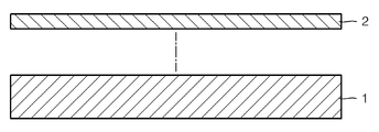
도 1은 본 발명의 바람직한 일 실시예에 따른 전기 영동 디스플레이 장치의 개략적인 구성을 도시한 단면도이다.1 is a cross-sectional view showing a schematic configuration of an electrophoretic display device according to an embodiment of the present invention.
도 1에서 볼 수 있듯이, 본 발명의 바람직한 일 실시예에 따른 전기 영동 디스플레이 장치는, 박막 트랜지스터를 포함하는 제1기판(1)과, 이 제1기판(1)의 일면에 결합되고, 전기 영동 입자 및 전기 영동 분산매를 포함하는 제2기판(2)과, 제2기판(2)의 일면에 결합되고, 칼라 필터를 포함하는 제3기판(3)을 포함한다.As shown in FIG. 1, an electrophoretic display device according to an exemplary embodiment of the present invention is coupled to a
도 2는 도 1의 전기 영동 디스플레이 장치의 일 실시예를 도시한 것이다.FIG. 2 illustrates an embodiment of the electrophoretic display device of FIG. 1.
먼저, 제1기판(1)은 제1베이스 기판(11)과 이 제1베이스 기판(11) 상에 형성된 박막 트랜지스터(12,13,14a,14b,15)를 포함한다.First, the
상기 제1베이스 기판(11)은 투명 또는 불투명한 기판이 사용될 수 있는 데, 글라스, 플라스틱, 또는 금속 호일이 사용될 수 있다. 상기 제1베이스 기판(11)으로는 플렉시블한 기판이 바람직한 데, 플라스틱재 기판이 바람직하다.As the
이 제1베이스 기판(11)의 일면에 게이트 전극(12)을 형성한다. 상기 게이트 전극(12)은 금속재로 단층 또는 복수층 적층하여 형성할 수 있는 데, 이 외에도, 금속 분말이 혼합된 고분자 페이스트 또는 전도성 고분자 등을 사용할 수 있다.The
이 게이트 전극(12)을 덮도록 게이트 절연막(13)을 형성한다. 게이트 절연막(13)은 단층 또는 복수층의 구조로 형성되어 있고, 유기물, 무기물, 또는 유/무기 복합물로 형성될 수 있다. 플렉시블한 디스플레이 장치를 구현하는 경우, 상기 게이트 절연막(13)도 유기물이 포함되도록 하는 것이 바람하다.A
상기 게이트 절연막(13) 상에 소스 전극(14a) 및 드레인 전극(14b)을 형성한다. 소스 전극(14a) 및 드레인 전극(14b)도 금속재로 단층 또는 복수층 적층하여 형성할 수 있는 데, 특히, Al, Mo, Au, Ag, Pt/Pd, Cu 등으로 형성할 수 있고, 이들 금속이 분말상으로 포함된 수지 페이스트를 도포할 수도 있으며, 전도성 고분자를 사용할 수도 있다.The
상기 게이트 절연막(13) 상에는 소스 전극(14a) 및 드레인 전극(14b) 사이에 이 소스 전극(14a) 및 드레인 전극(14b)에 각각 접하도록 활성층(15)을 형성한다.On the
이 활성층(15)은 유기 또는 무기 반도체재로 형성할 수 있는 데, 플렉시블한 디스플레이 장치를 구현하는 경우, 유기 반도체재로 형성하는 것이 바람직하다.The
상기 활성층(15)을 형성할 수 있는 유기 반도체 물질로는, 펜타센(pentacene), 테트라센(tetracene), 안트라센(anthracene), 나프탈렌(naphthalene), 알파-6-티오펜, 알파-4-티오펜, 페릴렌(perylene) 및 그 유도체, 루브렌(rubrene) 및 그 유도체, 코로넨(coronene) 및 그 유도체, 페릴렌테트라카르복실릭디이미드(perylene tetracarboxylic diimide) 및 그 유도체, 페릴렌테트라카르복실릭디안하이드라이드(perylene tetracarboxylic dianhydride) 및 그 유도체, 나프탈렌의 올리고아센 및 이들의 유도체, 알파-5-티오펜의 올리고티오펜 및 이들의 유도체, 금속을 함유하거나 함유하지 않은 프탈로시아닌(phthalocyanine) 및 이들의 유도체, 나프탈렌테트라카르복실릭디이미드(naphthalene tetracarboxylic diimide) 및 그 유도체, 나프탈렌테트라카르복실릭디안하이드라이드(naphthalene tetracarboxylic dianhydride) 및 그 유도체, 파이로멜리틱 디안하이드라이드 및 그 유도체, 파이로멜리틱 디이미드 및 이들의 유도체, 티오펜을 포함하는 공액계 고분자 및 그 유도체, 및 플루오렌을 포함하는 고분자 및 그 유도체 등이 사용될 수 있다.As an organic semiconductor material capable of forming the
무기 반도체재로는 아모퍼스 실리콘, 폴리 실리콘, 게르마늄 등의 반도체대가 사용될 수 있다.As the inorganic semiconductor material, semiconductor bands such as amorphous silicon, polysilicon and germanium may be used.
이상 설명한 박막 트랜지스터의 예는 바텀 게이트형 박막 트랜지스터의 구조를 취하고 있는 것이나, 본 발명이 반드시 이에 한정되는 것은 아니며, 게이트 전극이 활성층 상에 위치하는 탑 게이트형 박막 트랜지스터 등 다양한 구조의 박막 트랜지스터가 모두 적용 가능함은 물론이다.Examples of the thin film transistor described above take the structure of a bottom gate type thin film transistor, but the present invention is not necessarily limited thereto, and thin film transistors having various structures, such as a top gate thin film transistor in which a gate electrode is positioned on an active layer, are all Of course, it is applicable.
상기와 같이 박막 트랜지스터를 형성한 후에는 이 박막 트랜지스터를 덮도록 절연층(16)을 형성한 후, 이 절연층(16) 상에 픽셀 전극(17)을 형성한다. 픽셀 전극(17)을 형성할 때에는 절연층(16)에 형성된 비아 홀을 통해 픽셀 전극(17) 박막 트랜지스터의 드레인 전극(14b)과 콘택되도록 한다.After the thin film transistor is formed as described above, the
다음으로, 제2기판(2)은 전기 영동층(23)을 포함하도록 형성한다. Next, the
즉, 제2기판(2)은 제2베이스 기판(21)의 타면에 공통전극(22)을 형성한 후, 이 공통전극(22)의 타면에 전기 영동층(23)을 형성하여 구성한다.That is, the
상기 제2베이스 기판(21)은 투명한 기판으로 형성되는 것이 바람직한 데, 글라스 기판 또는 플라스틱 기판으로 형성될 수 있다. 그리고, 공통 전극(22)도 투명한 도전체로 형성될 수 있는 데, ITO, IZO, In2O3, ZnO등으로 형성할 수 있다.The
상기 전기 영동층(23)은 복수개의 전기 영동 볼(24)을 포함한다.The
각 전기 영동 볼(24) 내에는 전기 영동 분산매(24a)에 복수개의 서로 다른 색상의 제1,2전기 영동 분산입자(24b)(24c)들이 배치되어 있다. 제1전기 영동 분산입자(24b)와 제2전기 영동 분산입자(24c)는 서로 다른 극성을 띠도록 대전되어 있다. 따라서, 도 2에서 볼 수 있듯이, 공통 전극(22)과 픽셀 전극(17)에 전위차가 나도록 전압이 가해지면, 제1전기 영동 분산입자(24b)와 제2전기 영동 분산입자(24c) 공통 전극(22) 및 픽셀 전극(17)의 방향으로 각각 밀집되게 배치되어 이로써 소정의 화상이 구현되는 것이다.In each
상기와 같은 전기 영동층(23)의 구조는 반드시 도 2에 도시된 예에 한정되는 것은 아니며, 전기 영동 볼(24) 대신 격벽 구조체 내에 전기 영동 분산매와 전기 영동 입자들이 배치된 구조 등 다양한 구조로도 변형 가능하다.The structure of the
이렇게 제조된 제2기판(2)은 별도의 접착층(25)을 개재하여 제1기판(1)에 부착될 수 있다.The
이 때, 도 2에서는 픽셀 전극(17)이 제1기판(1)에 형성된 예만을 도시하였으나, 상기 픽셀 전극은 제2기판(2)의 제1기판(1)을 향한 면에 형성되고, 제1기판(1)에는 박막 트랜지스터에 연결된 콘택트(미도시)를 형성한 후, 이 콘택트와 픽셀 전극이 접속되도록 제1기판(1)과 제2기판(2)을 접합할 수도 있다.2 illustrates only an example in which the
한편, 제2기판(2)의 제2베이스 기판(21) 상에는 접착층(4)을 개재한 채로, 제3기판(3)이 접합될 수 있다.Meanwhile, the
제3기판(3)은 투명한 소재로 구비된 제3베이스 기판(31)과 이 제3베이스 기판(31) 상에 형성된 칼라 필터(32)로 구비될 수 있다. 제3베이스 기판(31)은 글라 스 기판 또는 플라스틱 기판이 바람직하나, 플렉시블 구현을 위해서는 플라스틱 기판이 바람직하다.The
이러한 도 2의 실시예에 따른 풀칼라 전기 영동 디스플레이 장치는 도 3a 내지 도 3c의 방법으로 제조될 수 있다.The full color electrophoretic display device according to the embodiment of FIG. 2 may be manufactured by the method of FIGS. 3A to 3C.
먼저, 도 3a에서 볼 수 있듯이, 제3기판(3)을 형성한다. 제3기판(3)은 전술한 바와 같이, 투명한 소재로 구비된 제3베이스 기판(31) 상에 칼라 필터(32)를 형성하여 구비된다. 칼라 필터(32)는 적색층(32a), 녹색층(32b), 청색층(32c) 등 화이트 구현이 가능한 색상으로 형성한다.First, as shown in FIG. 3A, a
다음으로, 도 3b에서 볼 수 있듯이, 별도로 제조된 제1기판(1)과 제2기판(2)을 준비하여, 이들을 서로 결합시킨다. 제1기판(1) 및 제2기판(2)의 구조는 전술한 도 2에서 설명한 바와 같다. 제1기판(1)과 제2기판(2)의 결합시에는 접착층을 개재하여 결합시킬 수 있다.Next, as can be seen in Figure 3b, a separately prepared
다음으로, 도 3c에서 볼 수 있듯이, 접착층(4)을 개재시켜 제3기판(3)을 제2기판(2) 상에 결합시킨다.Next, as shown in FIG. 3C, the
이 때, 제3기판(3)의 칼라 필터(32)의 각 색상층(32a)(32b)(32c)은 도 2에서 볼 수 있듯이, 픽셀 전극(17)에 대응되도록 얼라인시켜야 한다.At this time, each
제1기판(1)과, 제2기판(2)과, 제3기판(3)의 상호 간 결합 순서는 서로 바뀌어도 무방하다. 즉, 제2기판(2)과 제3기판(3)을 먼저 결합시킨 후, 제2기판(2)과 제1기판(1)을 결합시켜도 무방하다.The bonding order of the 1st board |
이렇게 별도로 칼라 필터를 포함하는 제3기판을 형성한 후, 이를 전기 영동 층을 갖는 제2기판에 접합함으로써, 간단하게 풀칼라 구현이 가능한 전기 영동 디스플레이 장치를 제조할 수 있다.By separately forming a third substrate including a color filter, and then bonding it to a second substrate having an electrophoretic layer, an electrophoretic display device that can be easily implemented in full color can be manufactured.
그러나, 이 방법의 경우, 제3기판(3)의 칼라 필터(32)의 각 색상층(32a)(32b)(32c)과, 픽셀 전극(17)의 얼라인 공정이 까다로울 수 있고, 이 때 불량이 발생할 여지도 있다. However, in this method, the alignment process of the
따라서, 도 4에 도시된 본 발명의 바람직한 일 실시예처럼 제3기판(3)의 칼라 필터(32)를 제2기판(2)의 제2베이스 기판(21)에 직접 형성할 수 있다.Therefore, as shown in FIG. 4, the
이 경우, 제3기판에 칼라 필터를 형성하기 위한 베이스 기판이 없게 되므로, 빛의 휘도를 더욱 증대시킬 수 있고, 제3기판(3)과 제2기판(2)의 까다로운 얼라인 공정을 피할 수 있어, 생산성을 더욱 증대시킬 수 있다.In this case, since there is no base substrate for forming the color filter on the third substrate, the brightness of the light can be further increased, and a difficult alignment process of the
도 5a 내지 도 5d는 도 4의 전기 영동 디스플레이 장치를 제조하는 일 실시예를 순차로 도시한 것이다.5A through 5D sequentially illustrate one embodiment of manufacturing the electrophoretic display device of FIG. 4.
먼저, 도 5a에서 볼 수 있듯이, 도너 기판(5)을 준비한다.First, as shown in FIG. 5A, the
도너 기판(5)은 제4베이스 기판(51) 상에 광열전환층(52: Light to Heat Conversion Layer, LTHC Layer)을 형성한 후, 이 광열전환층(52) 상에 피전사용 칼라 필터층(53)을 형성하여 제조한다.The
그 다음, 피전사용 칼라 필터층(53)이 제2기판(2)의 제2베이스 기판(21)을 향하도록 배치시킨다.Then, the
그리고, 도 5b에서 볼 수 있듯이, 픽셀에 대응되는 영역에 레이저를 조사한다. 이 레이저의 빛이 상기 광열전환층(52)에 의해 열로 전환되어 피전사용 칼라 필터층(53)을 제2베이스 기판(21) 상에 전사시킨다.As shown in FIG. 5B, the laser is irradiated to a region corresponding to the pixel. Light of the laser is converted into heat by the light-to-
그 다음, 도 5c에서 볼 수 있듯이, 도너 기판(5)을 떼어내면, 제2베이스 기판(21) 상에는 칼라 필터(32)가 형성되어 남게 된다.Then, as shown in FIG. 5C, when the
다음, 도 5d에서 볼 수 있듯이, 이렇게 칼라 필터(32)가 형성된 제2기판(2)을 박막 트랜지스터가 형성되어 있는 제1기판(1)과 얼라인한 후, 서로 접합한다.Next, as shown in FIG. 5D, the
위와 같은 방법을 사용할 경우, 제2기판(21) 상에 칼라 필터(32)를 한번에 직접 형성해 주므로, 두께를 더욱 얇게 할 수 있고, 이로 인해 휘도를 더욱 향상시킬 수 있다. 또한, 한번의 얼라인 공정만을 거치면 되므로, 생산성이 더욱 향상될 수 있다.In the case of using the above method, since the
도 6a 내지 도 6d는 도 4의 전기 영동 디스플레이 장치를 제조하는 다른 일 실시예를 순차로 도시한 것이다.6A to 6D sequentially illustrate another embodiment of manufacturing the electrophoretic display device of FIG. 4.
먼저, 6a와 같이, 제1기판(1)에 제2기판(2)을 결합시킨다. 이 때, 제2기판(2)은 도 2에서 도시된 구조를 가지므로, 제1기판(1)과 제2기판(2)의 결합은 정밀한 얼라인 작업이 필요없다.First, as shown in 6a, the
다음, 전술한 바와 같은 도너 기판(5)을 준비한 후, 이를 제2베이스 기판(21) 상에 배치시킨다. Next, after preparing the
그리고, 도 6c에서 볼 수 있듯이, 픽셀 전극(17)에 대응되는 위치에 레이저를 조사하여 피전사용 칼라 필터(53)를 제2베이스 기판(21)에 전사시킨다.As shown in FIG. 6C, a laser beam is irradiated to a position corresponding to the
그 다음, 도 6d에서 볼 수 있듯이, 도너 기판(5)을 떼어내면, 제2베이스 기판(21) 상에는 칼라 필터(32)가 형성되어 남게 된다.Then, as shown in FIG. 6D, when the
이 방법의 경우, 레이저 조사 위치의 제어만으로 간단하게 칼라 필터를 형성할 수 있으므로, 공정이 더욱 간단해지고 생산성이 향상될 수 있다.In this method, since the color filter can be formed simply by controlling the laser irradiation position, the process can be made simpler and the productivity can be improved.
상기한 바와 같이 이루어진 본 발명의 전기 영동 디스플레이 장치 및 그 제조방법에 따르면, 다음과 같은 효과를 얻을 수 있다.According to the electrophoretic display device and the manufacturing method of the present invention made as described above, the following effects can be obtained.
첫째, 간단한 방법으로 풀 칼라 전기 영동 디스플레이 장치를 구현할 수 있다.First, a full color electrophoretic display device can be implemented in a simple manner.
둘째, 풀 칼라 전기 영동 디스플레이 장치를 구현함에 있어, 생산성을 더욱 향상시킬 수 있다.Second, in implementing a full color electrophoretic display device, productivity may be further improved.
본 발명은 도면에 도시된 실시예를 참고로 설명되었으나 이는 예시적인 것에 불과하며, 본 기술 분야의 통상의 지식을 가진 자라면 이로부터 다양한 변형 및 균등한 다른 실시예가 가능하다는 점을 이해 할 것이다. 따라서 본 발명의 진정한 기술적 보호범위는 첨부된 특허청구범위의 기술적 사상에 의하여 정해져야 할 것이다.Although the present invention has been described with reference to the embodiments illustrated in the drawings, this is merely exemplary, and it will be understood by those skilled in the art that various modifications and equivalent other embodiments are possible. Therefore, the true technical protection scope of the present invention will be defined by the technical spirit of the appended claims.
Claims (13)
Priority Applications (5)
| Application Number | Priority Date | Filing Date | Title |
|---|---|---|---|
| KR1020070002660A KR20080065486A (en) | 2007-01-09 | 2007-01-09 | Electrophoretic display device and manufacturing method thereof |
| JP2007097312A JP2008170927A (en) | 2007-01-09 | 2007-04-03 | Electrophoretic display device and manufacturing method thereof |
| US11/736,138 US7893918B2 (en) | 2007-01-09 | 2007-04-17 | Electrophoretic display apparatus and manufacturing method thereof |
| CNA2007101092833A CN101221338A (en) | 2007-01-09 | 2007-05-29 | Organic electrophoretic display device and manufacturing method thereof |
| EP07252532A EP1944649A1 (en) | 2007-01-09 | 2007-06-22 | Electrophoretic display apparatus and manufacturing method thereof |
Applications Claiming Priority (1)
| Application Number | Priority Date | Filing Date | Title |
|---|---|---|---|
| KR1020070002660A KR20080065486A (en) | 2007-01-09 | 2007-01-09 | Electrophoretic display device and manufacturing method thereof |
Related Child Applications (1)
| Application Number | Title | Priority Date | Filing Date |
|---|---|---|---|
| KR1020090008392A Division KR20090028592A (en) | 2009-02-03 | 2009-02-03 | Electrophoretic display device and manufacturing method thereof |
Publications (1)
| Publication Number | Publication Date |
|---|---|
| KR20080065486A true KR20080065486A (en) | 2008-07-14 |
Family
ID=39272238
Family Applications (1)
| Application Number | Title | Priority Date | Filing Date |
|---|---|---|---|
| KR1020070002660A Ceased KR20080065486A (en) | 2007-01-09 | 2007-01-09 | Electrophoretic display device and manufacturing method thereof |
Country Status (5)
| Country | Link |
|---|---|
| US (1) | US7893918B2 (en) |
| EP (1) | EP1944649A1 (en) |
| JP (1) | JP2008170927A (en) |
| KR (1) | KR20080065486A (en) |
| CN (1) | CN101221338A (en) |
Families Citing this family (11)
| Publication number | Priority date | Publication date | Assignee | Title |
|---|---|---|---|---|
| US7781784B2 (en) * | 2007-05-07 | 2010-08-24 | Samsung Electronics Co., Ltd. | Display apparatus with color pixels |
| JP5428211B2 (en) * | 2008-06-13 | 2014-02-26 | セイコーエプソン株式会社 | Driving method of electrophoretic display device |
| KR101345172B1 (en) * | 2008-07-18 | 2013-12-27 | 엘지디스플레이 주식회사 | Electrophoretic display deivce |
| KR101276749B1 (en) * | 2009-08-03 | 2013-06-19 | 엘지디스플레이 주식회사 | Electrophoretic display device and manufacturing method thereof |
| TWI400549B (en) | 2010-06-01 | 2013-07-01 | Prime View Int Co Ltd | Method for manufacturing color electrophoretic display device |
| TWI547746B (en) | 2010-07-13 | 2016-09-01 | 元太科技工業股份有限公司 | Display device |
| CN102375281B (en) * | 2010-08-17 | 2015-12-02 | 元太科技工业股份有限公司 | monitor |
| JP5817134B2 (en) * | 2011-02-10 | 2015-11-18 | 凸版印刷株式会社 | Method for manufacturing electrophoretic display device and electrophoretic display device |
| CN102654705A (en) * | 2011-03-23 | 2012-09-05 | 京东方科技集团股份有限公司 | Electrophoretic display assembly and manufacturing method thereof |
| CN103186006A (en) * | 2011-12-29 | 2013-07-03 | 上海天马微电子有限公司 | Double-sided display electronic paper and electronic paper display |
| TWI490614B (en) * | 2013-01-24 | 2015-07-01 | E Ink Holdings Inc | Electrophoretic display apparatus |
Family Cites Families (36)
| Publication number | Priority date | Publication date | Assignee | Title |
|---|---|---|---|---|
| JP2575835B2 (en) * | 1988-08-25 | 1997-01-29 | 富士通株式会社 | Liquid crystal display for enlarged projection |
| JPH0777687A (en) * | 1993-09-10 | 1995-03-20 | Casio Comput Co Ltd | Liquid crystal display device and its manufacture |
| KR100271487B1 (en) * | 1997-05-23 | 2000-11-15 | 김순택 | Donor film for color filter |
| US6031594A (en) * | 1998-03-12 | 2000-02-29 | Engle; Craig D. | Electro-optic device |
| WO2000020923A1 (en) * | 1998-10-07 | 2000-04-13 | E Ink Corporation | Illumination system for nonemissive electronic displays |
| US6506438B2 (en) * | 1998-12-15 | 2003-01-14 | E Ink Corporation | Method for printing of transistor arrays on plastic substrates |
| US6597340B1 (en) * | 1999-03-05 | 2003-07-22 | Seiko Epson Corporation | Electrophoresis display and its production method |
| JP3667242B2 (en) * | 2000-04-13 | 2005-07-06 | キヤノン株式会社 | Electrophoretic display method and electrophoretic display device |
| JP4006925B2 (en) * | 2000-05-30 | 2007-11-14 | セイコーエプソン株式会社 | Method for manufacturing electrophoretic display device |
| KR100346550B1 (en) | 2000-06-13 | 2002-07-26 | 삼성에스디아이 주식회사 | Laser transfer |
| JP4165001B2 (en) | 2000-11-02 | 2008-10-15 | 富士ゼロックス株式会社 | Image display medium, image display device, and image display method |
| JP3925080B2 (en) | 2000-12-01 | 2007-06-06 | セイコーエプソン株式会社 | Electronic book and method of manufacturing electronic paper used therefor |
| KR20030034820A (en) | 2001-10-27 | 2003-05-09 | 삼성전자주식회사 | Reflective-transmissive type liquid crystal display device and method of manufacturing the same |
| JP2003270673A (en) * | 2002-03-15 | 2003-09-25 | Toppan Printing Co Ltd | Display panel and front panel for display panel |
| JP4206704B2 (en) * | 2002-07-31 | 2009-01-14 | セイコーエプソン株式会社 | Electrophoresis device manufacturing method, electrophoresis device, and electronic apparatus |
| US7388631B2 (en) * | 2002-10-10 | 2008-06-17 | Samsung Electronics, Co., Ltd. | Parallax compensating color filter and black mask for display apparatus |
| KR100940562B1 (en) | 2002-12-16 | 2010-02-03 | 삼성전자주식회사 | Organic semiconductor display |
| KR100906725B1 (en) | 2003-02-28 | 2009-07-07 | 엘지디스플레이 주식회사 | Color filter transfer film and manufacturing method of color filter substrate for liquid crystal display device using same |
| JP3941785B2 (en) * | 2003-03-13 | 2007-07-04 | セイコーエプソン株式会社 | Film forming method and color filter substrate manufacturing method |
| JP2005037851A (en) * | 2003-06-24 | 2005-02-10 | Seiko Epson Corp | Electrophoretic dispersion liquid, electrophoretic display device, electrophoretic display device manufacturing method, and electronic apparatus |
| US20050263903A1 (en) * | 2003-08-30 | 2005-12-01 | Visible Tech-Knowledgy, Inc. | Method for pattern metalization of substrates |
| US20050205999A1 (en) * | 2003-08-30 | 2005-09-22 | Visible Tech-Knowledgy, Inc. | Method for pattern metalization of substrates |
| JP2005114819A (en) * | 2003-10-03 | 2005-04-28 | Toppan Printing Co Ltd | Microcapsule type electrophoretic display panel and manufacturing method thereof |
| KR20050068794A (en) | 2003-12-30 | 2005-07-05 | 엘지.필립스 엘시디 주식회사 | The organic electro-luminescence device and method for fabricating of the same |
| JP4522101B2 (en) * | 2004-01-27 | 2010-08-11 | キヤノン株式会社 | Electrophoretic display device and driving method of electrophoretic display device |
| KR100611767B1 (en) | 2004-08-30 | 2006-08-10 | 삼성에스디아이 주식회사 | A method of manufacturing an organic electroluminescent device manufactured using a donor substrate for laser transfer and a film thereof |
| US20060062983A1 (en) * | 2004-09-17 | 2006-03-23 | Irvin Glen C Jr | Coatable conductive polyethylenedioxythiophene with carbon nanotubes |
| US7427441B2 (en) * | 2004-09-17 | 2008-09-23 | Eastman Kodak Co | Transparent polymeric coated conductor |
| US7825582B2 (en) * | 2004-11-08 | 2010-11-02 | Kyodo Printing Co., Ltd. | Flexible display and manufacturing method thereof |
| KR101133759B1 (en) * | 2004-12-28 | 2012-04-09 | 삼성전자주식회사 | Electrophoretic indication Display and Method for Manufacturing the same |
| US7038833B1 (en) * | 2005-01-25 | 2006-05-02 | Xerox Corporation | Encapsulated bichromal balls |
| ATE389896T1 (en) | 2005-04-21 | 2008-04-15 | Samsung Sdi Germany Gmbh | ACTIVE MATRIX CIRCUIT, ACTIVE MATRIX DISPLAY AND PROCESS OF PRODUCTION THEREOF |
| KR100953652B1 (en) * | 2005-08-18 | 2010-04-20 | 삼성모바일디스플레이주식회사 | Organic thin film transistor and its manufacturing method |
| US8446549B2 (en) | 2005-11-29 | 2013-05-21 | Creator Technology B.V. | Color filter to prevent color errors in a roll up display |
| JP5167624B2 (en) * | 2005-12-28 | 2013-03-21 | セイコーエプソン株式会社 | Electrophoretic display device and electronic apparatus |
| US7572667B2 (en) * | 2006-01-20 | 2009-08-11 | Samsung Electronics Co., Ltd. | Method of forming an organic semiconductor pattern and method of manufacturing an organic thin film transistor using the same |
-
2007
- 2007-01-09 KR KR1020070002660A patent/KR20080065486A/en not_active Ceased
- 2007-04-03 JP JP2007097312A patent/JP2008170927A/en active Pending
- 2007-04-17 US US11/736,138 patent/US7893918B2/en active Active
- 2007-05-29 CN CNA2007101092833A patent/CN101221338A/en active Pending
- 2007-06-22 EP EP07252532A patent/EP1944649A1/en not_active Withdrawn
Also Published As
| Publication number | Publication date |
|---|---|
| CN101221338A (en) | 2008-07-16 |
| JP2008170927A (en) | 2008-07-24 |
| US7893918B2 (en) | 2011-02-22 |
| US20080165121A1 (en) | 2008-07-10 |
| EP1944649A1 (en) | 2008-07-16 |
Similar Documents
| Publication | Publication Date | Title |
|---|---|---|
| KR20080065486A (en) | Electrophoretic display device and manufacturing method thereof | |
| CN101640252B (en) | Method for forming organic semiconductor thin film and method of manufacturing thin-film semiconductor device | |
| US8049217B2 (en) | Display device | |
| CN1797164B (en) | Electrophoretic display and its manufacturing method | |
| KR100683766B1 (en) | Flat panel display and manufacturing method | |
| US20100072482A1 (en) | Organic light emitting display and method of manufacturing the same | |
| TWI748166B (en) | Electronic device and manufacturing method of the same | |
| JP2012054575A (en) | Organic thin film transistor and flat plate indicating device equipped therewith | |
| CN109427848B (en) | OLED display panel and preparation method thereof, and OLED display device | |
| KR20130049785A (en) | Method for forming pattern, method for manufacturing light emitting device, and light emitting device | |
| US20080258138A1 (en) | Thin film transistor array panel and fabricating method thereof, and flat panel display with the same | |
| KR20120035040A (en) | Organic light emitting diode display apparatus and manufacturing method thereof | |
| JP2013030293A (en) | Display unit and substrate for display unit | |
| CN1832220B (en) | Method for manufacturing thin film transistor, thin film transistor and display device | |
| KR20140109169A (en) | Display device including thin film transistor | |
| JP2004233444A (en) | Active matrix display device and thin film transistor display device | |
| JP2012132960A (en) | Transistor array and connection method thereof | |
| KR20050093606A (en) | Electro-luminescence display device and method for producing the same | |
| CN1893108B (en) | Flat panel display and method of fabricating the same | |
| KR20090028592A (en) | Electrophoretic display device and manufacturing method thereof | |
| KR100670379B1 (en) | Organic thin film transistor, manufacturing method thereof and organic light emitting display device having same | |
| KR100647704B1 (en) | Organic thin film transistor, flat panel display device having same, manufacturing method of organic thin film transistor and manufacturing method of flat panel display device | |
| KR100751380B1 (en) | Organic light emitting display | |
| KR100749502B1 (en) | Method for manufacturing thin film transistor, thin film transistor manufactured by this method and display device comprising the thin film transistor | |
| CN100565901C (en) | Thin film transistor, manufacturing method thereof and flat panel display device having same |
Legal Events
| Date | Code | Title | Description |
|---|---|---|---|
| A201 | Request for examination | ||
| PA0109 | Patent application |
Patent event code: PA01091R01D Comment text: Patent Application Patent event date: 20070109 |
|
| PA0201 | Request for examination | ||
| E902 | Notification of reason for refusal | ||
| PE0902 | Notice of grounds for rejection |
Comment text: Notification of reason for refusal Patent event date: 20071206 Patent event code: PE09021S01D |
|
| E90F | Notification of reason for final refusal | ||
| PE0902 | Notice of grounds for rejection |
Comment text: Final Notice of Reason for Refusal Patent event date: 20080617 Patent event code: PE09021S02D |
|
| PG1501 | Laying open of application | ||
| N231 | Notification of change of applicant | ||
| PN2301 | Change of applicant |
Patent event date: 20081120 Comment text: Notification of Change of Applicant Patent event code: PN23011R01D |
|
| E601 | Decision to refuse application | ||
| E801 | Decision on dismissal of amendment | ||
| PE0601 | Decision on rejection of patent |
Patent event date: 20081205 Comment text: Decision to Refuse Application Patent event code: PE06012S01D Patent event date: 20080617 Comment text: Final Notice of Reason for Refusal Patent event code: PE06011S02I Patent event date: 20071206 Comment text: Notification of reason for refusal Patent event code: PE06011S01I |
|
| PE0801 | Dismissal of amendment |
Patent event code: PE08012E01D Comment text: Decision on Dismissal of Amendment Patent event date: 20081205 Patent event code: PE08011R01I Comment text: Amendment to Specification, etc. Patent event date: 20080818 Patent event code: PE08011R01I Comment text: Amendment to Specification, etc. Patent event date: 20080306 |
|
| J201 | Request for trial against refusal decision | ||
| PJ0201 | Trial against decision of rejection |
Patent event date: 20090105 Comment text: Request for Trial against Decision on Refusal Patent event code: PJ02012R01D Patent event date: 20081205 Comment text: Decision to Refuse Application Patent event code: PJ02011S01I Appeal kind category: Appeal against decision to decline refusal Decision date: 20090226 Appeal identifier: 2009101000050 Request date: 20090105 |
|
| A107 | Divisional application of patent | ||
| PA0107 | Divisional application |
Comment text: Divisional Application of Patent Patent event date: 20090203 Patent event code: PA01071R01D |
|
| PC1202 | Submission of document of withdrawal before decision of registration |
Comment text: [Withdrawal of Procedure relating to Patent, etc.] Withdrawal (Abandonment) Patent event code: PC12021R01D Patent event date: 20090219 |
|
| WITB | Written withdrawal of application | ||
| J301 | Trial decision |
Free format text: TRIAL DECISION FOR APPEAL AGAINST DECISION TO DECLINE REFUSAL REQUESTED 20090105 Effective date: 20090226 Free format text: TRIAL NUMBER: 2009101000050; TRIAL DECISION FOR APPEAL AGAINST DECISION TO DECLINE REFUSAL REQUESTED 20090105 Effective date: 20090226 |
|
| PJ1301 | Trial decision |
Patent event code: PJ13011S01D Patent event date: 20090226 Comment text: Trial Decision on Objection to Decision on Refusal Appeal kind category: Appeal against decision to decline refusal Request date: 20090105 Decision date: 20090226 Appeal identifier: 2009101000050 |