KR20080056129A - Current Sense Amplifiers for Voltage Converters - Google Patents
Current Sense Amplifiers for Voltage Converters Download PDFInfo
- Publication number
- KR20080056129A KR20080056129A KR1020080049904A KR20080049904A KR20080056129A KR 20080056129 A KR20080056129 A KR 20080056129A KR 1020080049904 A KR1020080049904 A KR 1020080049904A KR 20080049904 A KR20080049904 A KR 20080049904A KR 20080056129 A KR20080056129 A KR 20080056129A
- Authority
- KR
- South Korea
- Prior art keywords
- current
- gain
- amplifier
- signal
- output
- Prior art date
- Legal status (The legal status is an assumption and is not a legal conclusion. Google has not performed a legal analysis and makes no representation as to the accuracy of the status listed.)
- Abandoned
Links
- 238000012937 correction Methods 0.000 claims abstract description 37
- 238000000034 method Methods 0.000 claims abstract description 12
- 230000008859 change Effects 0.000 claims abstract description 8
- 230000003068 static effect Effects 0.000 claims description 6
- 230000001419 dependent effect Effects 0.000 claims description 5
- 238000009966 trimming Methods 0.000 claims description 4
- 230000008878 coupling Effects 0.000 claims description 3
- 238000010168 coupling process Methods 0.000 claims description 3
- 238000005859 coupling reaction Methods 0.000 claims description 3
- 238000005070 sampling Methods 0.000 claims 2
- 238000012544 monitoring process Methods 0.000 abstract description 7
- 101100317039 Aedes aegypti VGA1 gene Proteins 0.000 description 12
- 239000003990 capacitor Substances 0.000 description 10
- 238000010586 diagram Methods 0.000 description 9
- 230000003044 adaptive effect Effects 0.000 description 4
- 230000008569 process Effects 0.000 description 3
- 102220565243 L-lactate dehydrogenase A-like 6A_M11A_mutation Human genes 0.000 description 2
- 102220543961 RBPJ-interacting and tubulin-associated protein 1_M12A_mutation Human genes 0.000 description 2
- 230000001052 transient effect Effects 0.000 description 2
- 101100321311 Bacillus subtilis (strain 168) yxeG gene Proteins 0.000 description 1
- 101000597662 Homo sapiens Serine/threonine-protein phosphatase 2B catalytic subunit alpha isoform Proteins 0.000 description 1
- 102100035348 Serine/threonine-protein phosphatase 2B catalytic subunit alpha isoform Human genes 0.000 description 1
- 238000007906 compression Methods 0.000 description 1
- 230000006835 compression Effects 0.000 description 1
- 229920005994 diacetyl cellulose Polymers 0.000 description 1
- 238000005516 engineering process Methods 0.000 description 1
- 238000009472 formulation Methods 0.000 description 1
- 230000036039 immunity Effects 0.000 description 1
- 238000005259 measurement Methods 0.000 description 1
- 239000000203 mixture Substances 0.000 description 1
- 238000012986 modification Methods 0.000 description 1
- 230000004048 modification Effects 0.000 description 1
- 238000012806 monitoring device Methods 0.000 description 1
- 238000000819 phase cycle Methods 0.000 description 1
Images


Classifications
-
- G—PHYSICS
- G01—MEASURING; TESTING
- G01R—MEASURING ELECTRIC VARIABLES; MEASURING MAGNETIC VARIABLES
- G01R19/00—Arrangements for measuring currents or voltages or for indicating presence or sign thereof
- G01R19/32—Compensating for temperature change
-
- H—ELECTRICITY
- H03—ELECTRONIC CIRCUITRY
- H03F—AMPLIFIERS
- H03F1/00—Details of amplifiers with only discharge tubes, only semiconductor devices or only unspecified devices as amplifying elements
- H03F1/30—Modifications of amplifiers to reduce influence of variations of temperature or supply voltage or other physical parameters
-
- H—ELECTRICITY
- H02—GENERATION; CONVERSION OR DISTRIBUTION OF ELECTRIC POWER
- H02M—APPARATUS FOR CONVERSION BETWEEN AC AND AC, BETWEEN AC AND DC, OR BETWEEN DC AND DC, AND FOR USE WITH MAINS OR SIMILAR POWER SUPPLY SYSTEMS; CONVERSION OF DC OR AC INPUT POWER INTO SURGE OUTPUT POWER; CONTROL OR REGULATION THEREOF
- H02M3/00—Conversion of DC power input into DC power output
- H02M3/22—Conversion of DC power input into DC power output with intermediate conversion into AC
- H02M3/24—Conversion of DC power input into DC power output with intermediate conversion into AC by static converters
- H02M3/28—Conversion of DC power input into DC power output with intermediate conversion into AC by static converters using discharge tubes with control electrode or semiconductor devices with control electrode to produce the intermediate AC
Landscapes
- Physics & Mathematics (AREA)
- General Physics & Mathematics (AREA)
- Engineering & Computer Science (AREA)
- Power Engineering (AREA)
- Amplifiers (AREA)
Abstract
전압 컨버터를 위한 전류 감지 증폭기가 개시되는데, 여기서, 상기 전압 컨버터는 출력 인덕터를 통해 출력 전류를 제공하는 적어도 하나의 채널을 가지며, 상기 전류 감지 증폭기는 상기 출력 인덕터를 통해 상기 적어도 하나의 채널에서 전류를 모니터링하며, 상기 전류 감지 증폭기는 복수의 가변 이득 증폭기들을 포함하며(상기 전압 컨버터의 채널들보다 적어도 하나 이상 많은 가변 이득 증폭기가 있다), 이에 의해, 적어도 하나의 가변 이득 증폭기는 상기 가변 이득 증폭기가 오프셋 에러에 대해 보상되는 미리 정해진 시간 기간 동안에 보정 모드에 있으며, 상기 가변 이득 증폭기의 이득은 상기 출력 인덕터의 온도를 보상하도록 보정되며, 상기 미리 정해진 시간 기간 동안에, 모든 잔여의 가변 이득 증폭기들은 각 출력 인덕터에서 채널 전류를 모니터링하도록 연결된다. A current sense amplifier for a voltage converter is disclosed wherein the voltage converter has at least one channel providing an output current through an output inductor, wherein the current sense amplifier is current in the at least one channel through the output inductor. And the current sense amplifier comprises a plurality of variable gain amplifiers (there is at least one more variable gain amplifier than the channels of the voltage converter), whereby at least one variable gain amplifier is the variable gain amplifier. Is in the correction mode during a predetermined time period during which the offset error is compensated for, and the gain of the variable gain amplifier is corrected to compensate for the temperature of the output inductor, and during the predetermined time period, all remaining variable gain amplifiers The channel current in the output inductor It is coupled to monitoring.
본 발명에 따르면, 각 트랜지스터가 입력 전압이 공급되는 입력을 갖는 한 쌍의 트랜지스터들을 포함하는 차동 입력 증폭기를 포함하여 이루어진 가변 이득 증폭기가 제공되는데, 상기 트랜지스터들은 기준 전류를 제공하는 각각의 전류 소스를 직렬로 공급받도록 결합되며 여기서 전류는 트랜지스터들에 연결된 저항 소자를 걸쳐서 전개되며 이는 입력들 사이의 전압에 비례한다. 또한, 상기 트랜지스터 쌍의 트랜지스터와 각각 직렬로 결합된 트랜지스터들을 더 포함하여 이루어지며, 상기 추가 트랜지스터들은, 하나의 추가 트랜지스터내에서, 기준 전류 및 저항 소자내에서의 전류의 합, 그리고 다른 추가 트랜지스터내에서, 기준전류 및 저항 소 자내의 전류 사이의 차이와 실질적으로 동일한 전압이 입력들에 걸쳐서 공급되므로, 각각의 추가 트랜지스터에서 전류가 전개되도록 구성된다. 또한, 상기 합 및 차이 전류들이 곱해진 이득률과 동등한 전류를 전개하고 상기 저항 소자를 통하는 상기 전류가 곱해진 상기 이득률에 비례하는 출력전류를 전개하기 위한 이득 스테이지를 더 포함하여 이루어진다. 또한, 상기 출력 전류를 출력 전류 값으로 구동시키기 위해 상기 가변 증폭기의 상기 입력들에 걸친 변수에 비례하는 신호를 선택적으로 제공하기 위한 인터페이스를 더 포함하여 이루어진다. 그리고, 상기 출력 전류 값에 반응하고 상기 가변 이득 증폭기의 이득을 조절하는 이득 세팅 신호를 생성하는 이득 세팅 회로를 더 포함하여 이루어진다.According to the present invention there is provided a variable gain amplifier, wherein each transistor comprises a differential input amplifier comprising a pair of transistors having an input supplied with an input voltage, the transistors having respective current sources providing a reference current. Coupled to be fed in series, the current develops across a resistive element connected to the transistors, which is proportional to the voltage between the inputs. And further comprising transistors each coupled in series with the transistors of the transistor pair, wherein the additional transistors, in one additional transistor, sum of the reference current and the current in the resistance element, and in the other additional transistor. In, since a voltage substantially equal to the difference between the reference current and the current in the resistance element is supplied across the inputs, the current is configured to develop in each additional transistor. And a gain stage for developing a current equal to a gain ratio multiplied by the sum and difference currents and developing an output current proportional to the gain ratio multiplied by the current through the resistor element. The method further includes an interface for selectively providing a signal proportional to a variable across the inputs of the variable amplifier to drive the output current to an output current value. And a gain setting circuit for generating a gain setting signal responsive to the output current value and adjusting the gain of the variable gain amplifier.
또한, 본 발명에 따르면, 가변 이득 증폭기의 이득을 조절하기 위한 열 보정 회로가 제공되며, 상기 열 보정 회로는 온도에 따라 변하는 신호를 수신하고 온도 변화에 관계되는 신호를 제공하는 인터페이스; 입력 및 출력을 갖는 가변 이득 증폭기; 상기 입력에 선택적으로 결합되는 온도 변화에 관계되는 신호; 상기 가변 이득 증폭기의 출력에서 전개된 전류와 기준 전류 사이의 차이에 비례하는 제 1 전류를 전개하기 위한 상기 가변 이득 증폭기 출력에서의 회로를 포함하여 이루어지며, 상기 제 1 회로는 후속 회로를 구동하여 가변 이득 증폭기의 이득을 조절하는 이득 조절 신호를 생성한다.According to the present invention, there is also provided a thermal correction circuit for adjusting the gain of a variable gain amplifier, the thermal correction circuit comprising: an interface for receiving a signal varying with temperature and providing a signal relating to a temperature change; A variable gain amplifier having an input and an output; A signal related to a temperature change selectively coupled to the input; A circuit at the variable gain amplifier output for developing a first current proportional to the difference between the current developed at the output of the variable gain amplifier and a reference current, the first circuit driving a subsequent circuit to Generate a gain adjustment signal that adjusts the gain of the variable gain amplifier.
Description
관련출원Related application
본 출원은, 2006년 1월 18일자로 미국에 가특허출원된 "CURRENT SENSE AMPLIFIER FOR SENSING THE OUTPUT CURRENT OF A SWITCHING POWER SUPPLY, FOR EXAMPLE, OUTPUT INDUCTOR CURRENT OF A MULTI-PHASE BUCK CONVERTER"(가출원번호 60/759, 659)에 근거하며 이의 우선권을 주장한다. 상기 가특허출원의 전체 내용은 참조로서 본 출원에 인용된다.This application is filed under the provisional patent application of the United States on January 18, 2006, entitled "CURRENT SENSE AMPLIFIER FOR SENSING THE OUTPUT CURRENT OF A SWITCHING POWER SUPPLY, FOR EXAMPLE, OUTPUT INDUCTOR CURRENT OF A MULTI-PHASE BUCK CONVERTER" (provisional application number 60 / 759, 659). The entire contents of these provisional patent applications are incorporated herein by reference.
본 발명은, 예를 들어, 다중-위상 컨버터 또는 파워 서플라이와 같은 전압 컨버터내로 위상 또는 채널 전류들을 공급하는 출력 스테이지 또는 스테이지들의 전류를 감지하는 전류 감지 증폭기에 관한 것이다.The present invention relates, for example, to a current sense amplifier for sensing the current of an output stage or stages that supply phase or channel currents into a voltage converter such as a multi-phase converter or a power supply.
다중-위상 컨버터에서는, 예를 들면, 벅 컨버터(buck converter) 스테이지들과 같은 많은 수의 스위칭 파워 서플라이들이 파워 서플라이 제어기 및 드라이버 스테이지에 의해 제어된다. 각각의 위상 스테이지들은 DC 전압 버스에 걸쳐 결합되며, 전형적으로는 시간 위상 시퀀스(time phase sequence)내에서 출력 전류의 일 부를 제공한다.In a multi-phase converter, a large number of switching power supplies such as, for example, buck converter stages are controlled by the power supply controller and driver stage. Each phase stage is coupled across a DC voltage bus and typically provides a portion of the output current in a time phase sequence.
도1은 본 발명이 적용가능한 다중-위상 컨버터의 블록도이다. 도1은 2-위상 컨버터를 도시하고 있지만, 본 발명은 더 많은 위상을 갖는 컨버터에도 적용가능하다.1 is a block diagram of a multi-phase converter to which the present invention is applicable. Although Figure 1 shows a two-phase converter, the invention is also applicable to converters with more phases.
제어기(10)는, 전형적으로 펄스 폭 변조된(PWM) 제어 신호들을 제공하여 출력 스테이지들(20 및 30)의 턴-온을 제어한다. 제 1 출력 스테이지(20)는 출력 커패시터 C 양단에서 발달되는 컨버터의 출력에 제 1 출력 위상을 제공한다. 여기서는 벅 컨버터인 각각의 컨버터 출력 위상 스테이지는, DC 버스 VIN를 가로지르는 브리지(bridge)내에 연결되는 2개의 직렬 연결된 스위치들, 예를 들어 MOSFET, 을 포함하여 이루어진다. 각각의 스테이지는 하이 사이드 및 로우 사이드 트랜지스터를 포함하여 이루어지며, 이들은 2개의 스위치들의 온 시간들 사이의 데드 타임으로 상보적으로 스위치된다. 전형적으로 각각의 스테이지들(20 및 30)은 서로 다른 시간에서 출력 VOUT에 출력 전류를 공급하며, 하이 사이드 스위치들에 의해 공급되는 인덕터(L1 및 L2)내의 전류는 서로 다른 시간에 출력으로 흘러간다. 이러한 방법으로, 각각의 출력 스테이지는 VOUT에서 제공되는 전체 전류에 기여한다. 다중-위상 컨버터는 예를 들어, 개인용 컴퓨터들, 랩톱들, 및 서버들에 전형적으로 채용되며, 오늘날의 현대적인 마이크로프로세서에 요구되고 있는 2 볼트 미만의 낮은 전압들에서 매우 높은 전류를 제공할 수 있다. 잘 알려진 바와같이, 상기 하이 사이드 스위치는 인덕터에 전류를 제공하여 인턱터 및 출력 캐패시터를 충전하고 부하에 파워를 제공한다. 상기 하이 사이드 스위치가 오프되었을 때, 상기 로우 사이 드 스위치는 턴온되며 상기 부하에 인덕터 전류를 제공하기를 계속한다. 각각의 출력 스테이지는 정기의 시퀀스(timed sequence)에서 동작하며 각각의 하이 사이드 출력 트랜지스터는 서로 다른 시간에 부하로 출력 전류를 제공한다.The
제어기(10)가 도시된 도1에는 또한, 출력 VOUT에서 파워를 공급받는 CPU 마이크로프로세서 부하(15)가 도시되어 있다. 또한, 상기 마이크로프로세서는 많은 비트들로 이루어지며 요구되는 출력 전압을 제어기(10)로 알려주는 디지털 VID 신호를 제공하는 바, 이는 CPU의 동작 조건들(즉, CPU가 높은 파워 상태인지 또는 낮은 파워 상태인지)에 따라 변할 수 있다. 또한, 상기 제어기(10)는, 예를 들어, 상기 제어기(10)가 싱글(single) 작동인지 또는 2-채널(위상) 작동인지간에 계속적인 전도상태로 제어하는 것처럼, 출력 인덕터들(L1 및 L2)의 전도 상태를 제어하는 신호를 포함하여 CPU로부터의 추가적인 입력들을 가질 수도 있다. 또한, 열 모니터링 신호가 제어기(10)로부터 CPU로 공급될 수도 있으며, 열 모니터링 신호는 CPU로 하여금 파워 제어기(10)의 온도를 모니터링 할 수 있게 하는 열 모니터링 출력을 제공한다. Also shown in FIG. 1 where
또한, 상기 제어기(10)는 CPU 시스템 클럭을 시작하는 CLOCK ENABLE 신호와 지연 이후에 CPU를 초기화하는 신호를 제공한다. 또한, 제어기(10)는 제어기(10)를 활성화시키는 VR-ON 신호를 수신하며, 또 다른 프로세서에 의한 제어 또는 모니터링을 위해 가령, SM 버스와 같은 직렬 버스에 연결될 수도 있다. The
다중-위상 컨버터 회로들에서, 각각의 위상에서 전류 흐름을 조절하기 위해서는, 각 위상의 출력 전류에 대한 감지가 필요하며, 이는 적응성 전압 배치(adaptive voltage positioning)을 위해, 전류들을 등화시키기 위해, 과전류 조건을 모니터하기 위해서이다.In multi-phase converter circuits, in order to regulate the current flow in each phase, sensing of the output current of each phase is necessary, which is necessary for equalizing the currents for adaptive voltage positioning, overcurrent. To monitor the condition.
본 발명은 각각의 위상 또는 채널에서의 전류를 정확히 감지하는 다중 위상 컨버터용 전류 감지 증폭기에 관한 것이며, 전류 감지 증폭기에서의 오프셋 전압들을 보상하고 각 위상에서의 온도 변화들을 보상하기 위해 보정을 유지한다. 전류 감지 증폭기의 기능들은 2개 채널들 또는 위상들 각각에서의 전류를 감지하는 것인데, 이는 과도전류 보호를 유지하고, 채널들 사이에서 전류 균형을 유지하며, 제어 IC가 높은 부하 전류에서 낮은 전압으로 조절하는 것 같은[적응성 전압 배치(adaptive voltage positioning : AVP) 또는 droop 로 알려짐], 원하는 부하 라인 작동(load line behavior)을 제공하기 위함이다. The present invention relates to a current sense amplifier for a multiple phase converter that accurately senses current in each phase or channel, and maintains a correction to compensate for offset voltages in the current sense amplifier and to compensate for temperature variations in each phase. . The functions of the current sense amplifiers are to sense current in each of two channels or phases, which maintains transient protection, balances current between channels, and allows the control IC to move from high load current to low voltage. Such as to adjust (known as adaptive voltage positioning (AVP) or droop), to provide the desired load line behavior.
본 발명에 따른 전류 감지 증폭기는 DCR 전류 감지를 사용하도록 디자인되었으며, DCR 전류 감지에서는 각각의 출력 인덕터의 DC 고유 저항에 걸리는 전압이 모니터링되어 출력 전류를 결정한다. 당업계에 알려진 바와 같이, DCR 전류 감지에서는, 직렬 RC 필터가 출력 인덕터 양단에 배치되며, 증폭기가 RC 필터의 캐패시터에 걸리는 전압을 모니터링하여 인덕터 전류를 감지하는데, 이때 인덕터와 직렬로 연결된 추가적인 감지 저항을 도입하지 않고도 인덕터 전류를 감지할 수 있으며 상기 인덕터와 직렬로 연결된 추가적인 감지 저항을 도입하는 것은 전력 손실을 야기할 수도 있다. 높은 입력 임피던스를 제공하도록 MOS 입력 디바이스들이 증폭기내에서 통상적으로 사용된다. The current sense amplifier according to the present invention is designed to use DCR current sensing, in which the voltage across the DC intrinsic resistance of each output inductor is monitored to determine the output current. As is known in the art, in DCR current sensing, a series RC filter is placed across the output inductor, and the amplifier senses the inductor current by monitoring the voltage across the capacitor of the RC filter, with an additional sense resistor in series with the inductor. The inductor current can be sensed without the need to introduce and introducing an additional sense resistor in series with the inductor may cause power loss. MOS input devices are commonly used in amplifiers to provide high input impedance.
본 발명에 따르면, 온도에 따른 인덕터 저항의 변화를 보상하기 위해 가변 이득 증폭기가 사용된다. 더 나아가, RC 회로의 캐패시터에 걸쳐서 공급되는 작은 입력 신호에 대한 정확한 측정을 가능케 하기 위해서, 능동 오프셋 보정이 사용된다. According to the present invention, a variable gain amplifier is used to compensate for variations in inductor resistance with temperature. Furthermore, active offset correction is used to enable accurate measurements on small input signals supplied across the capacitors of the RC circuit.
본 발명은 예를 들면, Intel 사의 IMVP-VI mobile CPU 파워 사양에 맞게 디자인되었다. The present invention is designed to meet the IMVP-VI mobile CPU power specification of Intel Corporation, for example.
본 발명에 따르면, 컨버터내의 채널들보다 적어도 하나 이상 많은 증폭기가 제공된다. 이러한 방법으로, 적어도 하나 이상인 증폭기가 항상 보정되고 있으며, 다른 증폭기들은 채널 전류들을 능동적으로 모니터링한다. 예를 들면, 2-위상 또는 2-채널 컨버터의 경우, 3개의 가변 이득 증폭기들이 제공된다. 3개의 증폭기들중 2개는 출력 채널들내의 전류를 각각 모니터하도록 제공된다. 다른 2개의 증폭기들이 각각의 출력 인덕터들 내의 전류를 감지하는 시간동안에 3번째 증폭기가 보정된다. 상기 가변 이득 증폭기들은 상태 테이블에 따라 동작하여 시간 순서(time sequence)내에서 출력 스테이지들내의 전류들을 감지하도록 순환(rotate)한다. 따라서, 가장 최근(most recently)에 보정되었던 가변 이득 증폭기가 가장 먼저 보정되었던 가변 이득 증폭기를 대체한다. 가변 이득 증폭기는 오프셋 및 온도 모두를 보상하기 위해 보정된다. 이후에, 이러한 절차들이 반복되는 바, 최근에 보정되었던 가변 이득 증폭기는 가장 이전에(least recently) 보정되었던 가변 이득 증폭기를 대체하며, 대체되었던 증폭기가 보정되는 동안에 최근에 보정되었던 가변 이득 증폭기 및 나머지 가변 이득 증폭기가 출력전류들을 각각 감지한다. 상기 대체된 가변 이득 증폭기는, 보정된 이후에, 가장 이전에 보정되었던 다음 가변 이득 증폭기를 대체하며 그리고 상기 절차가 계속된다. 이러한 방법을 통해, 2-채널 다중-위상 컨버터에 대한 3개의 가변 이득 증폭기를 포함하여 이루어진 전류 감지 증폭기는, 항상 보정 상태내에 있음을 지속할 수 있다.According to the invention, at least one or more amplifiers are provided than the channels in the converter. In this way, at least one amplifier is always being calibrated and other amplifiers actively monitor the channel currents. For example, in the case of a two-phase or two-channel converter, three variable gain amplifiers are provided. Two of the three amplifiers are provided to monitor the current in the output channels respectively. The third amplifier is calibrated during the time when the other two amplifiers sense the current in their respective output inductors. The variable gain amplifiers operate according to a state table to rotate to sense the currents in the output stages in a time sequence. Thus, the variable gain amplifier that was most recently corrected replaces the variable gain amplifier that was corrected first. The variable gain amplifier is calibrated to compensate for both offset and temperature. Subsequently, these procedures are repeated: the recently corrected variable gain amplifier replaces the last recently corrected variable gain amplifier, and the recently corrected variable gain amplifier and the rest while the replaced amplifier is being corrected. The variable gain amplifier senses each of the output currents. The replaced variable gain amplifier, after being corrected, replaces the next variable gain amplifier that was previously corrected and the procedure continues. In this way, a current sense amplifier made up of three variable gain amplifiers for a two-channel multi-phase converter can continue to be in the calibration state at all times.
본 발명은 또한, 신규의 오프셋 및 온도 이득 보정회로를 포함할 뿐만 아니라 각각의 출력 채널 내의 전류를 감지하는데 사용되는 신규의 가변 이득 증폭기를 포함하여 이루어진다. The invention also includes a novel offset and temperature gain correction circuit as well as a novel variable gain amplifier used to sense the current in each output channel.
본 발명에 따르면, 각 트랜지스터가 입력 전압이 공급되는 입력을 갖는 한 쌍의 트랜지스터들을 포함하는 차동 입력 증폭기를 포함하여 이루어진 가변 이득 증폭기가 제공되는데, 상기 트랜지스터들은 각 트랜지스터가 기준 전류를 제공하는 각각의 전류 소스에 직렬로 제공되도록 연결되어 있고, 여기서 전류는 트랜지스터들에 연결된 저항 소자에 걸쳐서 발달하며 이는 입력들 사이의 전압에 비례한다. 또한, 가변 이득 증폭기는 상기 트랜지스터 쌍의 트랜지스터에 각각 직렬로 연결된 트랜지스터들을 더 포함하여 이루어지며, 상기 추가 트랜지스터들은, 각각의 추가 트랜지스터에서 전류가 발달하도록 구성되는데, 이는 입력들에 걸리는 공급 전압이 실질적으로 하나의 추가 트랜지스터 내에서의 기준 전류 및 저항 소자 내에서의 전 류의 합과 동일하고, 그리고 다른 추가 트랜지스터 내에서, 기준전류 및 저항 소자 내의 전류 사이의 차이와 실질적으로 동일함에 의한 것이다. 또한, 가변 이득 증폭기는 상기 합 및 차이 전류들이 곱해진 이득률(gain factor)과 동등한 전류를 발달시키고 상기 저항 소자에 흐르는 상기 전류가 곱해진 상기 이득률에 비례하는 출력전류를 발달시키기 위한 이득 스테이지를 더 포함하여 이루어진다. 또한, 가변 이득 증폭기는 상기 출력 전류를 출력 전류 값으로 구동하기 위해 상기 차동 증폭기의 상기 입력들에 걸친 변수에 비례하는 신호를 선택적으로 제공하기 위한 인터페이스를 더 포함하여 이루어진다. 그리고, 가변 이득 증폭기는 상기 출력 전류 값에 대해 응답하는 회로로서 상기 가변 이득 증폭기의 이득을 조절하기 위해 이득 세팅 신호를 생성하는 이득 세팅 회로를 더 포함하여 이루어진다.According to the present invention there is provided a variable gain amplifier, wherein each transistor comprises a differential input amplifier comprising a pair of transistors having an input to which an input voltage is supplied, each transistor providing a respective reference current. Connected to be provided in series with the current source, where the current develops across a resistor element connected to the transistors, which is proportional to the voltage between the inputs. In addition, the variable gain amplifier further comprises transistors each connected in series to the transistors of the pair of transistors, wherein the additional transistors are configured to develop current in each additional transistor, so that the supply voltage across the inputs is substantially By the sum of the reference current in one additional transistor and the current in the resistive element, and substantially the same as the difference between the reference current and the current in the resistive element in the other additional transistor. In addition, a variable gain amplifier develops a current equal to a gain factor multiplied by the sum and difference currents, and a gain stage for developing an output current proportional to the gain multiplied by the current flowing through the resistance element. It further comprises. The variable gain amplifier further comprises an interface for selectively providing a signal proportional to the variable across the inputs of the differential amplifier to drive the output current to an output current value. The variable gain amplifier further includes a gain setting circuit that generates a gain setting signal to adjust the gain of the variable gain amplifier as a circuit responsive to the output current value.
또한, 본 발명에 따르면, 가변 이득 증폭기의 이득을 조절하기 위한 열 보정 회로가 제공되며, 상기 열 보정 회로는 온도에 따라 변하는 신호를 수신하고 온도 변화에 관계되는 신호를 제공하는 인터페이스; 입력 및 출력을 갖는 가변 이득 증폭기; 상기 입력에 선택적으로 결합되는 온도 변화에 관계되는 신호; 상기 가변 이득 증폭기의 출력에서 발달한 전류와 기준 전류 사이의 차이에 비례하는 제 1 전류를 발달시키기 위한 상기 가변 이득 증폭기 출력에서의 회로를 포함하여 이루어지며, 상기 제 1 회로는 추가적 회로를 구동하여 가변 이득 증폭기의 이득을 조절하는 이득 조절 신호를 생성한다.According to the present invention, there is also provided a thermal correction circuit for adjusting the gain of a variable gain amplifier, the thermal correction circuit comprising: an interface for receiving a signal varying with temperature and providing a signal relating to a temperature change; A variable gain amplifier having an input and an output; A signal related to a temperature change selectively coupled to the input; A circuit at the variable gain amplifier output for developing a first current proportional to the difference between the current developed at the output of the variable gain amplifier and the reference current, the first circuit driving additional circuitry to Generate a gain adjustment signal that adjusts the gain of the variable gain amplifier.
본 발명의 다른 특징들 및 장점들은 첨부된 도면을 참조하여 설명되는 아래에 기술된 발명의 상세한 설명에서 명확해질 것이다. Other features and advantages of the present invention will become apparent from the following detailed description of the invention which is described with reference to the accompanying drawings.
본 발명은 각각의 위상 또는 채널에서의 전류를 정확히 감지하는 다중 위상 컨버터용 전류 감지 증폭기에 이용된다.The present invention is used in current sense amplifiers for multiple phase converters that accurately sense current in each phase or channel.
이제 도2를 참조하면, 도2는 도1에 도시된 것과 유사하며, 본 발명의 전류 감지 증폭기가 적용될 수 있는 2-채널 다중-위상 컨버터를 도시하고 있다. 비록 2 채널 컨버터가 도시되었지만, 본 발명은 1 채널 또는 3 채널 이상의 컨버터에도 적용가능하다. 예를 들면, 단일 위상 컨버터에서, 2개의 가변 이득 증폭기가 사용될 수 있으며, 이들 중 하나는 임의의 시간 상에서 보정 상태에 있다. 3 위상 컨버터의 경우, 4개의 증폭기(또는 그 이상)가 사용될 수 있다.Referring now to FIG. 2, FIG. 2 is similar to that shown in FIG. 1 and shows a two-channel multi-phase converter to which the current sense amplifier of the present invention can be applied. Although a two channel converter is shown, the invention is also applicable to one or three or more converters. For example, in a single phase converter, two variable gain amplifiers can be used, one of which is in a calibrated state at any time. In the case of a three phase converter, four amplifiers (or more) may be used.
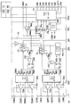
제어기(10)는, 채널 1의 트랜지스터 Q1 및 Q2 와 채널 2 의 트랜지스터 Q3 및 Q4의 턴온 및 턴 오프를 위한 위상 구동 신호를 제공한다. 부하를 공급하는 출력 VOUT 으로 각각의 채널에 의해 공급되는 전류는, 전술한 바와 같은 DCR 기술을 사용하여 모니터링되는 바, 인덕턴스 L1, L2(이상적인 인덕터 L1, L2 및 이들의 상응하는 고유 저항들 또는 DCR 이라고 도시됨) 각각에 걸쳐서 있는 채널 1에 대한 R1C1 회로와 채널 2에 대한 R2C2 회로를 포함하여 이루어진 RC 필터 회로를 위치시킴으로써 모니터링된다. 각각의 인덕터의 상기 DCR 및 온도는 변할 수도 있기 때문에, 각각의 채널은, 제어기(10)내에 제공되는 전류 감지 증폭기에 연결된 고유의 RC 회로를 갖는다. 또한, 온도 디바이스 NTC(예를 들어, 서미스터)가 입력 RT 와 VOUT 사이에 연결된다. 또한, 저항 소자 RTG(예를 들면, 정밀 저항)가 단자 RTG 와 출력 VOUT 사이에 연결되는 바, 이에 대해서는 후에 상세히 설명된다. 채널 1에 대해, 입력 CS1 및 VO1 에 걸친 전류가 모니터된다. 채널 2에 대해, 입력 CS2 및 VO2 에 걸친 전류가 모니터된다. The
도3은 제어기(10)에 대한 블록도이다. 도시된 전류 감지 증폭기(CSA)(90)는 디지털 상태 머신(90A)에 의해 제어되며, 그 동작은 상세히 후술될 것이다. 디지털 상태 머신(90A)은 3개의 가변 이득 증폭기들의 순환을 제어하며, 이는 도4를 참조하여 상세히 설명된다. 임의의 시간에서, 가변 이득 증폭기들 중 2개는 2개의 채널들 내의 전류들을 모니터링하며, 그동안 3번째 가변 이득 증폭기가 보정된다. 상기 상태 머신(90A)은, 가장 최근에 보정되었던 증폭기 스테이지가 가장 이전에 보정되었던 증폭기를 대체하도록 주기적으로 순환시킨다. 상기 CSA(90)는 2개의 채널들 내의 전류들을 균형잡는 균형 신호 BAL, 2개의 채널들 내의 과도 전류를 방지하기 위한 2개의 과전류 제한들인 OCLIMIT1, OCLIMIT2, 적응성 전압 배치(AVP)를 위한 신호인 DROOP 를 포함하여 이루어진 출력들을 생성한다. CSA(90)는 입력들인 CS1, VO1 및 CS2, VO2를 통해 2개의 채널들로부터 입력들을 수신하며, 온도 인터페이스(240)으로부터 온도 의존 신호인 IPTC 를 수신한다. 또한 상기 CSA(90)는, 임의의 오프셋들에 대해 가변 이득 증폭기들을 내부적으로 균형잡아 주는 오프셋 보상 신호를 출력한다.3 is a block diagram of the
도4는 전류 감지 증폭기의 전체 회로를 도시한 도면이다. 도시된 바와 같이, 상기 회로는, 채널 1 P 및 N, 채널 2 P 및 N, 보정 입력인 보정(Calibration, CAL) P 및 N 의 6개의 입력을 수신하는 입력 멀티플렉서(100)를 포함한다. 후자의 2개의 입력은 제어기(10)의 외부 단자들이 아니다. 상기 입력 멀티플렉서는 전류 감지 증폭기 멀티플렉서 제어 상태 머신으로부터의 12 bit 신호를 포함하여 이루어진 디지털 제어 신호에 의해 제어된다.Fig. 4 shows the entire circuit of the current sense amplifier. As shown, the circuit includes an
상기 입력 멀티플렉서는, 채널 1, 채널 2, 및 보정 입력들로부터의 연속된 입력들을 선택하여 3개의 가변 이득 증폭기들(110, 120, 및 130)로 공급한다. 2개의 전류 감지 채널들은 항상 2개의 선택된 가변 이득 증폭기(VGAs)로 공급되며 동시에 3번째 VGA가 보정된다. 가변 이득 증폭기들의 출력들은 P1 및 N1 P2 및 N2, P3 및 N3 이다. 전술한 바와같이, 임의의 시간에서 2개의 VGAs는 2개의 입력 채널들을 모니터링하고 있고, 3번째 VGA는 보정중에 있다. 도6은 상태 테이블을 도시한 도면이다. 도시된 바와같이, 도6에는 6개의 상태들이 있다. 상태 1에서, 채널 1 과 채널 2가 VGA 1 및 VGA 2 에 각각 연결된다. 상기 VGA 3는 보정 모드에 있다. 상태 2에서, 가장 최근에 보정되었던 VGA 3는, 가장 이전에 보정되었던 VGA 인 VGA 1을 대체하고, VGA 1이 상태 2에서 보정된다. VGA 2는 채널 2와의 연결을 유지한다. 상태 3에서, VGA 2가 보정되며, VGA 1가 채널 2 위치로 순환된다. VGA 3는 변화가 없다. 상태 4에서는, VGA 3가 가장 먼저 보정되었던 것이 되므로, 따라서 이제는 VGA 3가 보정되며, VGA 1은 채널 2에 연결된 상태로 남고 VGA 2는 VGA 3를 대체하여 채널 1에 연결된다. 이와 유사한 순환이 상태 5와 상태 6에 대해서도 계속되며 상태 6 이후에 상기 상태들은 도시된 것처럼 반복된다. The input multiplexer selects successive inputs from
도21은 입력 멀티플렉서의 연결들과 하나의 상태에서 도6에 도시된 상태 테이블에 상응하는 다음번 상태로의 상태 변화들을 도시한다. FIG. 21 shows the connections of the input multiplexer and state changes from one state to the next state corresponding to the state table shown in FIG.
도4로 돌아가서, 각 VGAs(110, 120, 130)의 출력들은 전류 분배기(splitter) 1, 전류 분배기 2, 및 전류 분배기 3 (140, 150, 160)로 공급되며, 상기 전류 분배기들은 이득 조절된 전류들을 출력 멀티플렉서(120)로 공급한다. 상태 머신 제어기(90A)의 디지털 제어하에서, 상기 출력 멀티플렉서(120)는, 이러한 전류들을 트랜스임피던스 증폭기(transimpedance amplifier : TZA), 전류 균형 회로, 과전류 보호 회로(LIMIT 1 및 LIMIT 2)로 공급하며, 또한 오프셋 트리밍 회로(offset trimming circuit)로 오프셋 신호를 공급한다. 4, the outputs of each VGAs 110, 120, 130 are fed to
전술한 바와 같이, 하나의 VGA는 항상 보정모드에 있다. 보정 순서(calibration sequence)는, VGA 오프셋 보정을 제공하도록 연속 근사 레지스터(successive approximation register : SAR) 를 사용하는 오프셋 조절 루틴을 포함하는 바, 이에 대해서는 도19를 참조하여 후술될 것이다. 또한, 인덕터 저항(inductor resistance)의 온도 계수를 보상하기 위해 이득을 조절하는 온도 보정 루틴 역시, 도20을 참조하여 조만간 후술될 것이다.As mentioned above, one VGA is always in correction mode. The calibration sequence includes an offset adjustment routine that uses a successive approximation register (SAR) to provide VGA offset correction, which will be described below with reference to FIG. In addition, a temperature correction routine for adjusting the gain to compensate for the temperature coefficient of inductor resistance will also be described later with reference to FIG.
도 19는 보정 모드에 있을 때의 각 VGA(110, 120, 및 130)에 대해 수행되는 오프셋 전압 보정의 시간에 있어서의 도면을 보여준다. 오프셋 보정은, VGA 내에서의 오프셋 전압이 그 정확도를 유지하도록 조절하기 위해, 수행된다. 이것은 VGA의 차동 입력에서 저항기를 통과하는 전류를 트리밍(trimming) 함으로써 수행된다. 오프셋 보정을 수행하기 위해, VGA로의 입력은 도 19에서의 111에서 보이는 바와 같이 단락된다. 입력 멀티플렉서(100)는 도 19에서 보이지 않는다. 그러나 입력들은, 보정되는 VGA에 대한 도 4의 입력들 CALP 및 CALN를 단락시킴으로써, 단락된다. 차 동 출력들을 포함하는 VGA의 출력은 보이는 오프셋 보정 회로에 의해 균등하게 되며, 이 회로는 오프셋 보정을 구현하기 위해 비교기(210), 연속 근사 레지스터(Successive Approximation Register, SAR) 및 제어 로직(22) 그리고 전류 스티어링(steering) DAC(Digital to Analog Converter)(230)를 포함한다. VGA의 차동 입력들은 전류 미러(320) 안으로 공급되고 그리고 오프셋 비교기(210)에 공급된다. 비교기(210)의 출력은 전류 스티어링 디지털 대 아날로그 컨버터(230)를 제어하는 디지털 레지스터(220)에 제공된다. DAC(230)의 출력은 오프셋을 보상하기 위해 VGA 안으로 스티어링되는 차동 전류이다. 3개의 DAC가 존재하며, 각 VGA에 대해 하나이다. DAC(230)의 출력은 TRIM-P 및 TRIM-N이며, 이것의 목적은 도 22와 연결되어 더 명확하게 될 것이다.FIG. 19 shows a plot in time of offset voltage correction performed for each
VGA 오프셋 보정 다음은 도 20에 도시된 온도 보정이다. 인덕터의 온도는 외부 서미스터 NTC에 의해 얻어진다. 단지 하나의 서미스터가 도 2의 두 개의 채널 컨버터에 대해 보여진다. 추가적인 서미스터가, 예를 들어 후속 회로의 추가와 함께, 두 번째 채널에 대해 제공될 수 있다. 더욱이, 만약 컨버터가 추가 채널들을 가진다면, 더 많은 서미스터들이 제공될 수 있다. 정밀 저항기 RTG 컨버터들은 IC에 의해 내부적으로 공급된 전류 기준을 전압 기준으로 변환시킬 수 있다. 도 2를 참조하라. 보정 중에 VGA의 입력은 서미스터 인터페이스(240)로부터의 온도 신호 I-TEMP에 의해 조정된다. VGA는 피드백 루프 내에서 고정되며, 그 출력은 전류 소스 IREF에 의해 일정한 레벨로 강제된다. 이 루프는 이득을 제어하여 심지어 온도와 함께 변하는 입력의 조건 아래에서도 VGA는 일정한 출력 레벨을 발생한다. 이 이득 제어 전압은 이 보정 동안 샘플링되고 이후에 VGA 내의 샘플-홀드 캐패시터 상에서 유지된다. VGA Offset Correction The following is the temperature correction shown in FIG. The temperature of the inductor is obtained by an external thermistor NTC. Only one thermistor is shown for the two channel converter of FIG. Additional thermistors may be provided for the second channel, for example with the addition of subsequent circuits. Moreover, if the converter has additional channels, more thermistors can be provided. Precision resistor RTG converters can convert the current reference supplied internally by the IC to a voltage reference. See FIG. 2. The input of VGA during calibration is adjusted by the temperature signal I-TEMP from
서미스터 인터페이스(240)의 출력은, 보정 중인 VGA로 입력 전압을 생산하기 위해 저항기 RPOLY를 통해 제공되는 온도 신호 I-TEMP를 포함하는, 전류이다. VGA 차동 출력 전류는 전류 미러(250)에 의해 종료되는 싱글로 변환된다. 이 싱글 종료 전류는 IREF에 저항하며, 이 전류들에서의 차이는 소스 연결 쌍(260)(정적 바이어스(static bias)와 함께 제공됨)를 드라이브하여 이득 제어 신호 I-GAIN을 산출한다. I-GAIN 신호는 열 입력에 기반을 둔 VGA 이득을 조정한다.The output of
디지털 상태 머신(90A)은 보정 시퀀스와 증폭기들의 회전을 제어한다. 입력 멀티플렉서(100)와 출력 멀티플렉서(170)는 도 6에서 보이는 6 가지 다른 상태에서 3 개의 VGA의 구성을 허용한다. 프로그램 가능한 대기 시간 이후, 예를 들어 2 밀리초 이후에, VGA는 보정된다. 보정 직후에, 보정된 VGA는 가장 최근에 보정된 서비스 중인 VGA를 대체한다. 브레이크 접속 전에 메이크 비포 브레이크(make before break) 연결이 입력들에서 사용된다. 이것은 보정된 증폭기가 그것의 출력이 이전에 서비스 중인 VGA를 대체하기 전에 입력 채널에 접속되고 안정되게 한다. 이 방식에서, 오프셋 보정 및 온도 보상은 2 밀리초 마다 리프레시 된다.
각 VGA의 출력은 차동 전류 신호를 포함한다. 이 신호는 각각 전류 분배기(160)(도 4)로의 입력이며, 이 각각은 정확한 매칭에 대해 최적화된 전류 미러들의 세트이다. 각 전류 분배기의 출력은 3 개의 실질적으로 동일한 차동 전류 신호들이다. A, B, 및 C; D, E, 및 F; 그리고 G, H, 및 I. 3 갱의 전류 분배기가 있으 며, 각 VGA에 대해 하나이다. 이러한 출력 전류는, 도 4에서 도시된 바와 같이, 출력 멀티플렉서(170)로 제공된다.The output of each VGA includes a differential current signal. These signals are each input to current divider 160 (FIG. 4), each of which is a set of current mirrors optimized for exact matching. The output of each current divider is three substantially identical differential current signals. A, B, and C; D, E, and F; And there are G, H, and I.3 gang current dividers, one for each VGA. This output current is provided to the
그 다음에 출력 멀티플렉서는 5 개의 차동 출력 신호들 TZA, 밸런스(balnce), LIMIT 1, LIMIT 2(과전류에 대해서는 양쪽 모두) 그리고 오프셋을 제공한다.The output multiplexer then provides five differential output signals, TZA, balance,
도 5로 돌아가서, 출력 멀티플렉서(170)은 5 개의 출력 채널들 TZA, 밸런스(balnce), LIMIT 1, LIMIT 2(과전류에 대해서는 양쪽 모두) 그리고 오프셋 상에 VGA의 출력들을 제공한다.Returning to FIG. 5,
두 쌍의 차동 전류 신호들은(각 채널로부터 하나), 합쳐지고 그리고 그 다음으로 광범위한 컴플라이언스(compliance) 전류 미러(180)에 인가되어 다중위상 컨버터에 의해 전해진 전체 전류에 비례하는 싱글 엔디드(single ended) 전류를 산출한다. 이 싱글 엔디드 전류는 전압 출력의 부하 라인을 조절하는데 사용되는 DROOP 신호를 산출하는 트랜스임피던스(transimpedence) 증폭기(TZA AMP(190))에 공급된다. 이 신호는 증가하는 부하 전류로 출력 전압이 감소하도록 하는데 사용되고 또한 적응성 전압 배치(Aadaptive Voltage Positioning, AVP)로 알려져 있다. 이 신호는 도 2 및 3 에서의 DROOP 출력 핀 상에 존재하고 그리고 증가하는 부하 전류로 출력 전압을 감소시키도록 하기 위해 피드백 입력으로 피드백된다.Two pairs of differential current signals (one from each channel) are combined and then single ended, applied to a wide range of compliance
전류 분배기들(각 채널로부터 하나)로부터의 다음 두 쌍의 차동 전류 신호는, 광범위한 컴플라이언스 전류 미러(300)에 인가되기 전에 도 5에서 밸런스(BALANCE)로 이름 붙여진 신호를 산출하기 위해 감산되는데, 이는 두 개의 채널 에 의해 전달된 전류에서의 차이에 비례하는 싱글 엔디드 전류를 산출하기 위함이다. 이 신호는 컨버터의 각 채널에 의해 전달되는 전류의 균형을 맞추기 위해 사용된다. 도 2 및 3을 참조하면, 이것은 신호 BAL에 존재한다. BAL 신호는 하나 또는 양쪽 모두의 램프(ramp) 발생기(52)들에 제공되어 PWM 램프(RAMP)가 출력들에서 전류들의 균형을 맞추도록 하고, 그럼으로써 컨버터의 각 채널에 의해 전달되는 전류의 균형을 맞춘다.The next two pairs of differential current signals from current dividers (one from each channel) are subtracted to yield a signal named BALANCE in FIG. 5 before being applied to a wide range of compliance current mirrors 300. This is to calculate a single ended current proportional to the difference in current delivered by the two channels. This signal is used to balance the current delivered by each channel of the converter. 2 and 3, this is in the signal BAL. The BAL signal is provided to one or both
각 전류 분배기로부터의(즉, 각 채널에 대해서) 차동 전류 신호들의 세 번째 쌍은 각각의 광범위한 컴플라이언스 전류 미러들(310)에 인가되어 각 채널을 제한하는데 사용되는 두 개의 싱글 엔드 신호들을 발생시킨다. 이러한 신호들은 LIMIT 1 및 LIMIT 2로 이름 붙여지고 그리고 도 3에서 라인 OC(OverCurrent, 과전류)(54)에, DAC 및 속도 제어(56)로 이름 붙여진 블록에 제공되어 과전류 제한을 설정한다.A third pair of differential current signals from each current divider (ie for each channel) is applied to each broad compliance
마지막으로 보정에서 VGA(130)(도 4)의 출력은 전류 분배기(160)에 인가된다. 하나의 차동 전류는 오프셋 트리밍을 위해 간단하고 정확하게 매칭되는 크로스-콰드(cross-quad) 전류 미러(320)에 인가된다. 도 19의 SAR 오프셋 비교기(210)는 이 전류 미러 양단에 연결된다. 전류 미러(320)의 다이오드 접속 디바이스(320A)는 양의 비교기 입력에 인가되고 반면에 미러의 출력은 음의 입력에 인가된다. 어떠한 이른(early) 전압 에러도 발생되지 않는데, 이것은 SAR 루틴(routine)이 비교기(210)의 입력을 같도록 이끌기 때문이다. 이것은 미러 디바이스(320B)의 드레인-소스 전압이 다이오드 접속 미러 디바이스(320A)의 게이트-소스 전압과 같을 때 발 생한다.Finally in calibration the output of VGA 130 (FIG. 4) is applied to
도 4의 전류 분배기(160)의 두 번째 차동 전류 출력은 열 보상 동안 보정된 VGA 둘레의 피드백 루프를 둘러싸는데 사용된다. 이것은 미러(250)에 의해 도 20에서 보여지고 그리고 앞서 설명되었다.The second differential current output of
도 6의 상태 테이블로 돌아가서 그리고 도 7를 참조하여, 도 7은 상태 1에서의 전류 감지 증폭기의 시간에 있어서의 스냅샷을 보여준다. 보이는 바와 같이, 상태 1에서의 3 개의 VGA, VGA1, VGA2, VGA3은 연결되어 있어 VGA1은 입력으로 채널 1을 가지고, VGA2는 입력으로 채널 2를 가지고 그리고 나머지 VGA3은 보정 내에 있다. 도 7에서, 출력 멀티플렉서(170)뿐만 아니라 입력 멀티플렉서(100)는 보이지 않는데 그것은 그들이 단지 스위치들에 불과하고 명확하기 때문이다. 입력 멀티플렉서(100)는 VGA들 각각의 차동 입력을 채널 1(CS1 및 VO1) 그리고 채널 2 입력(CS2 및 VO2) 그리고 서미스터 NTC 셀(240) 출력 전류 노드 IPTC에 연결한다. 전자 스위치 S1(입력 멀티플렉서의 부분)는 서미스터 신호 IPTC 및 VO1을 VGA 입력에 연결한다. 신호 IPTC는 양의 온도 계수를 가진 전류이다. 전류 분배기들로부터의 3 개의 동일한 차동 전류 출력(도 7에서는 도시되지 않음)은 출력 멀티플렉서(170)에 의해, 도 5와 관련되어 앞서 설명된 것으로서 차동 신호를 싱글 엔디드 신호들로 변환시키는, 전류 미러에 연결된다. 이 전류 미러들은 도 7에서 U2 내지 U6에서 나타내진다. 도 7에서, 전류 분배기들(140, 150 및 160)은 도시된 VGA들 안으로 통합된다. 도 7에서 209에서 보이는 바와 같이, 보정 동안, 보정 내의 VGA의 다른 두 개의 차동 쌍은 단락된다.Returning to the state table of FIG. 6 and with reference to FIG. 7, FIG. 7 shows a snapshot in time of the current sense amplifier in
도 8은 상태 1에서의 입력 멀티플렉서를 보여준다. 보이는 바와 같이, 입력 CS1 및 VO1은 VGA1의 입력에 제공된다. 채널 2 입력 CS2 및 VO2는 VGA 입력들에 제공되고 그리고 IPTC 양단의 열 입력 및 VO1은 세 번째 VGA에 제공된다. IPTC는 NTC(PIN RT) 및 RTG (도 2)에 연결된 것으로서 VO1에 기준을 둔 열 인터페이스 회로(240)로부터 유도된다.8 shows an input multiplexer in
도 9 내지 14는 6 가지 상태들 각각 내에서의 출력 멀티플렉서를 보여준다. 보이는 바와 같이, 예를 들어 도 9에서, 상태 1에서, VGA1으로부터의 제 1 차동 쌍은 VGA2의 제 1 차동 쌍인 TZA에 제공된다. VGA3의 제 1 차동 쌍은 단락된다.9-14 show output multiplexers in each of the six states. As can be seen, for example, in FIG. 9, in
VGA1 및 VGA2로부터의 제 2 차동 쌍들은 밸런스 신호를 형성하기 위해 제공 되는데, 이 신호는 도 3에서의 하나 또는 양쪽 모두의 램프 발생기(52)에 공급되어 채널들 각각 내에서의 전류의 균형을 맞춘다. 이러한 것은 도 9에서 RAMP P 및 RAMP N으로 표시된다.Second differential pairs from VGA1 and VGA2 are provided to form a balance signal, which is supplied to one or both
VGA1 및 VGA2의 세 번째 차동 전류 쌍은 앞서 언급된 바와 같이 전류 제한 신호를 형성하고 그리고 과전류 보호 신호 OC를 형성하는데 사용된다.The third differential current pair of VGA1 and VGA2 is used to form the current limiting signal and form the overcurrent protection signal OC as mentioned above.
보정 내에서의, VGA3으로부터의 차동 전류 신호들의 제 2 쌍은 또한 단락되고 그리고 제 1 쌍에 연결된다. VGA3으로부터의 차동 전류 신호들의 마지막 쌍은, 도 5를 참조하여 설명된 바와 같이 오프셋 발생을 위해 그리고 후속되는 열 보정을 위해 보정 입력에 제공된다. 대안적으로, 후속 전류 분배기 출력은 열 보정을 위해 사용될 수 있다.Within the correction, the second pair of differential current signals from VGA3 are also shorted and connected to the first pair. The last pair of differential current signals from VGA3 is provided to the correction input for offset generation and for subsequent thermal correction as described with reference to FIG. 5. Alternatively, the subsequent current divider output can be used for thermal correction.
잔여의 도 10 내지 14는 다른 상태 2 내지 6에서의 출력 멀티플렉서의 접속 들을 보여주며 그리고 이것은 도면으로부터 명백하며 본원에서 더 세부적으로 설명될 필요가 없다.The remaining FIGS. 10-14 show connections of the output multiplexer in different states 2-6 and this is evident from the figure and need not be described in more detail herein.
*도 15는 입력 멀티 플렉서 테이블을 보여주며 그리고 여러 가지 상태에서의 VGA의 접속들을 요약한다. 예를 들어, 상태 1에서, VGA1은 채널 1에 접속된 입력을 가지며, VGA2는 채널 2에 접속된 입력을 가지며, 그리고 VGA3은 VOUT과 IPTC 사이에 접속된 입력, 즉 써미스터 셀의 출력을 가진다. 상태 2에서, VGA1이 가장 먼저 보정되었었기 때문에, 그것은 지금 보정 내에 있고, VGA3이 이제 VGA1을 대신한다. VGA2는 채널 2에 접속된 상태를 유지하고 그리고 VGA3은 지금 채널 1에 접속된다. 예제를 하나 더 제공하기 위해, 상태 3에서, VGA2는 지금 보정 내에 있고, VGA3은 채널 1에 접속된 상태를 유지하고 그리고 VGA1은 지금 채널 2에 접속된다.Figure 15 shows the input multiplexer table and summarizes the connections of VGA in various states. For example, in
도 16 내지 18은 각각 VGA1, VGA2, 및 VGA3 각각에 대한 출력 멀티플렉서 테이블을 나타낸다. 예를 들어, 도 16에서, IP1A, IN1A, IP2A, IN2A 및 IP3A, IN3A는 도 7의 VGA1의 출력이다(또는 도 4의 분배기 스티어링3 개의 차동 전류 출력 A, B, 및 C). 이러한 테이블들은 앞서 설명된 접속들을 한층 더 요약한다. 도 16 내지 18 각각에서, VGA의 입력 접속은 상부 3 개의 행에서 요약되고, 그리고 출력 접속들은 하부 6개의 행에서 요약된다.16-18 show output multiplexer tables for VGA1, VGA2, and VGA3, respectively. For example, in FIG. 16, IP1A, IN1A, IP2A, IN2A and IP3A, IN3A are the outputs of VGA1 of FIG. 7 (or divider steering 3 differential current outputs A, B, and C of FIG. 4). These tables further summarize the connections described above. In each of Figures 16-18, the input connections of the VGA are summarized in the top three rows, and the output connections are summarized in the bottom six rows.
이제 도 22로 돌아가면, 이 도면은 각 VGA의 개념적 동작을 설명한다. 이 VGA는 가변 이득, 그라운드(ground)를 포함하는 넓은 입력 공통 모드 범위, 넓은 차동 신호 범위 그리고 VREF에 의해 지시되는 넓은 가변의 레벨로 언급될 수 있는 출력을 제공하도록 설계된다.Returning now to FIG. 22, this figure illustrates the conceptual operation of each VGA. This VGA is designed to provide an output that can be referred to as a variable gain, a wide input common mode range with ground, a wide differential signal range, and a wide variable level indicated by VREF.
각 VGA는 마이너스 100 밀리볼트에서 플러스 100 밀리볼트의 바이폴라 차동 전류 신호 범위를 수용한다. 이 범위는 신호 압축이 없는 바이폴라 곱셈기에 대해서는 너무 넓다.Each VGA accepts a bipolar differential current signal range of minus 100 millivolts to plus 100 millivolts. This range is too wide for bipolar multipliers without signal compression.
표준 트랜스컨덕턴스(GM) 셀 프론트 엔드(front end)에서와 같이, 입력 디바이스들 M1 및 M2의 쌍은 소스 I2 및 I3에 의해 일정한 전류에서 구동된다. 이것은 매칭된 디바이스들에 대해서 차동 입력 신호는 저항기 R1 양단에 나타난다는 것을 의미한다. 이러한 방식에서, 트랜스컨덕턴스는 1/R1에 설정된다. VGA 입력은 Inn 및 Inp이다. 디바이스들 M1 및 M2는 에러를 최소화하기 위해 커다란 트랜스컨덕턴스에 대해 크기 조절된다.As in the standard transconductance (GM) cell front end, the pair of input devices M1 and M2 are driven at a constant current by sources I2 and I3. This means that for matched devices, the differential input signal appears across resistor R1. In this way, the transconductance is set at 1 / R1. VGA inputs are Inn and Inp. Devices M1 and M2 are scaled for large transconductance to minimize errors.
VGA 회로는 대칭적이고 양의 입력 신호 및 음의 입력 신호 모두에 대해 동일한 방식으로 동작한다. 양의 신호에 대해, 저항기 R1을 통과하는 전류로서 VIN/R1과 동일한 전류 IX는 도시된 방향에서 R1을 통과하여 흐른다. 음의 신호에 대해, 전류는 R1을 통과하여 반대방향으로 흐른다. 도시된 전류는 캐스코드(cascode) M4가 전류 I+IX를 운반하도록 하고 그리고 캐스코드 M3은 I-IX를 운반하도록 하는데 여기서 I는 전류 소스 I2 및 I3에 의해 입력 쌍 디바이스 M1 및 M2를 통해 강제되는 일정한 바이어스 전류이다.The VGA circuitry is symmetrical and operates in the same way for both positive and negative input signals. For a positive signal, a current IX equal to VIN / R1 as the current through resistor R1 flows through R1 in the direction shown. For negative signals, current flows through R1 in the opposite direction. The illustrated current causes cascode M4 to carry current I + IX and cascode M3 carries I-IX, where I is forced through input pair devices M1 and M2 by current sources I2 and I3. Constant bias current.
저항기 R3, R4, R5 및 R6은 3극(triod) 모드에서 동작하는 MOSFET들을 나타낸다. 이것은 전자적으로 가변 저항기들이다. R3의 저항은 M3의 I-IX 전류를 운반하도록 조절되고 반면에 R4의 저항은 M4 I+IX 전류를 운반하도록 조절된다.Resistors R3, R4, R5 and R6 represent MOSFETs operating in triod mode. These are electronically variable resistors. The resistance of R3 is adjusted to carry the I-IX current of M3, while the resistance of R4 is adjusted to carry the M4 I + IX current.
전압 소스 V1은 M3 및 M4의 게이트에 인가되는 VCASC 볼트의 값을 가진다. M3 및 M4와 함께 이 전압 소스는 R3 및 R4 양단 전압을 설정한다.Voltage source V1 has a value of VCASC volts applied to the gates of M3 and M4. Together with M3 and M4, this voltage source sets the voltage across R3 and R4.
전압 소스 V4는 이득 제어 전압을 나타내고 그리고 M5 및 M6과 함께 R5 및 R6 양단 전압을 설정한다. VGAIN으로 명명된 소스 V4의 전압은 양이거나, 음이거나 또는 제로(0)일 수 있다. 그것이 제로로 설정되는 경우, R3 내지 R6을 포함한 모든 가변 저항들 양단의 전압 강하는 동일하다. Voltage source V4 represents the gain control voltage and sets the voltage across R5 and R6 along with M5 and M6. The voltage of source V4, named VGAIN, can be positive, negative, or zero. If it is set to zero, the voltage drop across all variable resistors, including R3 through R6, is the same.
가변 저항 R3 및 R5는 동일한 전자 제어 신호에 의해 구동된다. 마찬가지로, 저항 R4 및 R6은 동일한 제어 신호에 의해 구동된다. 저항 R3, R4, R5 및 R6은 또한 물리적 레이아웃(layout)에서 어울리고 연결되도록 설정된다.The variable resistors R3 and R5 are driven by the same electronic control signal. Similarly, resistors R4 and R6 are driven by the same control signal. The resistors R3, R4, R5 and R6 are also set to match and connect in the physical layout.
저항기 R5는 R3에 연결되기 때문에, 제로로 설정된 VGAIN에 대해, M5는 M3(I-IX)와 동일한 전류를 운반한다. 마찬가지로, 저항기 R6이 R4에 연결되기 때문에, M6은 M4(I+IX)와 동일한 전류를 운반한다.Since resistor R5 is connected to R3, for VGAIN set to zero, M5 carries the same current as M3 (I-IX). Likewise, because resistor R6 is connected to R4, M6 carries the same current as M4 (I + IX).
0이 아닌 이득 값들에 대해, 백 엔드(back end) 디바이스들 M5 및 M6에서의 전류는 프론트 엔드(front end) 디바이스들 M3 및 M4 내에서의 스케일링 된 버전의 전류이다. 스케일 비율(scale factor)은 도 22에서 K로 도시되어 있고 이는 1보다 더 크거나 더 작을 수 있다. 따라서, 전류 K(I-IX)는 M5 내에서 흐르고 그리고 전류 K(I+IX)는 M6 내에서 흐르다.For non-zero gain values, the current at back end devices M5 and M6 is a scaled version of current in front end devices M3 and M4. The scale factor is shown as K in FIG. 22, which may be larger or smaller than one. Thus, current K (I-IX) flows in M5 and current K (I + IX) flows in M6.
디바이스들 M7 및 M8은 차동 입력 신호를 싱글 종료 신호로 변환하는 전류 미러를 형성한다. 이러한 방식에서, 바이어스 전류가 빠지게 되고 그리고 결과적인 신호 전류 2KIX는, 트랜스임피던스 증폭기 TZA(190)로서 기능하는 이상적 연산 증 폭기를 포함하는 연산 증폭기(190) 둘레의 피드백 루프 내에 연결된 피드백 저항기 R2를 통해 흐른다. 출력 멀티플렉서(170)는 명확하기에 도시되지 않았다. 출력 VOUT은 도 5의 신호 DROOP를 포함한다. 이것은 또한 도 3에서 도시된다.Devices M7 and M8 form a current mirror that converts the differential input signal into a single termination signal. In this way, the bias current is released and the resulting signal current 2KIX is via feedback resistor R2 connected in a feedback loop around the
출력은 VOUT = 2KIXR2이며 여기서 IX=VIN/R1이며 그래서 결과적인 이득은 VO/VIN = 2K(RT/R1)이다. VGA의 출력 신호는 VREF로 도시되어 있는 OP-AMP(190)의 기준 입력에 인가된 전압으로 언급된다.The output is VOUT = 2KIXR2, where IX = VIN / R1, and the resulting gain is VO / VIN = 2K (RT / R1). The output signal of the VGA is referred to as the voltage applied to the reference input of the OP-
앞서 설명된 바와 같이, VGA의 오프셋을 조절하기 위해, 저항기 R1을 통과하는 전류는 도 19의 전류 스티어링 DAC(230)에 의해 트리밍되며, 이것은 저항기 R1 양단에 연결된 아날로그 출력을 가지며, 이것은 단자 TRIM-P 및 TRIM-N을 포함한다. 도 19 및 22를 참조하라. VGA로의 입력들이 단락되는 경우, R1를 통과하는 전류가 0이 되도록, R1 내의 전류를 조절함으로써, VGA의 오프셋은 보상된다.As described above, to adjust the offset of the VGA, the current through resistor R1 is trimmed by
도 23, 24 및 25는 모두 각 VGA의 개략도를 나타낸다. 도 23은 본원에서 VGA 프런트 엔드로 언급되는 것을 보여주며, 도 24는 본원에서 백 엔드로 언급되는 것을 보여주며, 그리고 도 25는 바이어스 회로를 보여준다. 이 도면들은 도 22에서 도시된 VGA 개념 모델을 구현한다. 도 23과 도 25 사이에는 약간의 겹쳐진 부분이 있다. 문자 A-L은 두 도면들 사이의 대응하는 접속 포인트들을 지시한다.23, 24 and 25 all show schematic diagrams of each VGA. FIG. 23 shows what is referred to herein as the VGA front end, FIG. 24 shows what is referred to herein as the back end, and FIG. 25 shows the bias circuit. These figures implement the VGA conceptual model shown in FIG. There is a slight overlap between FIGS. 23 and 25. Letter A-L indicates the corresponding connection points between the two figures.
특히, VGA 프런트 엔드는 도 22에서와 같이 유사하게 명명된 트랜지스터 M1 및 M2를 포함한다. 저항기 R1은 이득을 설정하고 그리고 도 22에서의 저항기 R1에 대응한다. 트랜지스터 M5 및 M5A는 도 22에서의 가변 저항기 R3에 대응하며, 그리고 트랜지스터 M6 및 M6A는 도 22에서의 가변 저항기 R4에 대응한다.In particular, the VGA front end includes similarly named transistors M1 and M2 as in FIG. Resistor R1 sets the gain and corresponds to resistor R1 in FIG. Transistors M5 and M5A correspond to variable resistor R3 in FIG. 22, and transistors M6 and M6A correspond to variable resistor R4 in FIG. 22.
M1과 M2의 게이트들 사이의 차동 입력 전류가 제로인 상태에서, 전류 I는 M1 및 M2 양쪽 모두에 의해 운반된다. 이 전류의 반, (I/2)는 정적 트라이오드(static triode) FET M5 및 M6에 의해 운반된다. 도 19의 DAC(230)는 오프셋을 보상하기 위해 R1을 통과하는 전류를 공급한다.With the differential input current between the gates of M1 and M2 equal to zero, current I is carried by both M1 and M2. Half of this current, (I / 2), is carried by static triode FETs M5 and M6. The
OPAMP I250은 M5A의 게이트(노드 N11)를 구동하여 그 저항을 변경하도록 하며, 그래서 R14 및 M1 내에서의 전류가 변하는 입력 신호와 함께 일정하도록 한다. OPAMP I251은 R24 및 M2 내에서의 전류가 일정하도록 M6A(노드 N12)의 게이트를 구동시킨다.OPAMP I250 drives the gate of M5A (node N11) to change its resistance, so that the current in R14 and M1 is constant with the changing input signal. OPAMP I251 drives the gate of M6A (node N12) so that the current in R24 and M2 is constant.
OPAMP A2-1은 전압 NCASC에 대한 M5 및 M5A의 소스들을 구동한다. 이것은 신호 전류, 온도 및 공정에서 변하는 캐스코드 M3의 게이트-소스 전압에 의해 발생되는 에러를 제거한다. OPAMP A2-2는 트라이오드 FET M6 및 M6A에 대해 동일한 기능을 한다.OPAMP A2-1 drives the sources of M5 and M5A for voltage NCASC. This eliminates errors caused by the gate-source voltage of cascode M3, which varies in signal current, temperature and process. OPAMP A2-2 functions the same for triode FETs M6 and M6A.
캐스코드 디바이스들은 그 관련된 OPAMP들과 함께 M5, M5A, M6 및 M6A가 3극 영역에서 동작하는 것을 확실하게 한다. 공칭 드레인-소스 전압 100 밀리볼트는 유지된다.Cascode devices, along with their associated OPAMPs, ensure that M5, M5A, M6 and M6A operate in the three-pole region. The nominal drain-source voltage of 100 millivolts is maintained.
트라이오드 FET는 정적 디바이스와 가변 저항 디바이스로 나누어진다. 이것은, 제어 루프가 브랜치(branch)를 제로 전류 상태로 만들 수 없기에 시동 문제를 피하기 위해서 수행되는 것이다. 또한 이것은 두 피드백 루프 제제 1 제어 M5A와 제 2 제어 M6A 사이의 결합(coupling)을 감소시킴으로써 안정성 문제를 피한다.Triode FETs are divided into static devices and variable resistance devices. This is done to avoid startup problems since the control loop cannot bring the branch to zero current. This also avoids stability issues by reducing the coupling between the two
두 루프 사이의 결합 소자는 저항기 R1이다. 심지어 최대 차동 입력 전압을 가지고, 저항기 R1을 통과하는 전류가 M5A 또는 M6A 피드백 루프 중 어느 하나를 턴 오프 하거나 포화시킬 수 없도록 바이어스가 설정된다.The coupling element between the two loops is the resistor R1. Even with the maximum differential input voltage, the bias is set such that the current through resistor R1 cannot turn off or saturate either the M5A or M6A feedback loop.
노드 NCASC에서의 캐스코드 전압은 도 25에서 도시된 저항 R30을 통과하는 시스템 기준 전류를 끌어냄으로써 발생된다. 이 시스템 전류는 폴리레지스터(polyresistor) 양단에 밴드갭(bandgap) 기준 전압을 인가함으로써 발생된다. R30은 또 다른 폴리레지스터이기 때문에, 그 양단 전압은 밴드갭 정확성과 저항기 매칭 정확성에 의해 제한된 정확성을 가진다. 이것은 양의 공급 레일 VDDL에 기준을 둔 정확한 캐스코드 전압을 제공한다.The cascode voltage at node NCASC is generated by drawing a system reference current through resistor R30 shown in FIG. This system current is generated by applying a bandgap reference voltage across the polyresistor. Since R30 is another polyregister, the voltage across it has accuracy limited by bandgap accuracy and resistor matching accuracy. This provides an accurate cascode voltage based on the positive supply rail VDDL.
도 24는 VGA 백 엔드 배선도를 보여준다. 이 백 엔드에서, 디바이스 M11 및 M11A는 도 22에서의 가변 저항기 R5에 대응하고, 반면에 디바이스 M12 및 M12A는 가변 저항기 R6에 대응한다.24 shows a VGA back end wiring diagram. At this back end, devices M11 and M11A correspond to variable resistor R5 in FIG. 22, while devices M12 and M12A correspond to variable resistor R6.
프런트 엔드 디바이스 M5A를 구동하는 OPAMP I250는 또한 저항에 연결되도록 노드 N11을 통해 백 엔드 디바이스 M11A를 구동시킨다.OPAMP I250, which drives front-end device M5A, also drives back-end device M11A through node N11 to be connected to a resistor.
프런트 엔드 디바이스 M6A를 구동하는 OPAMP I251는 또한 저항에 연결되도록 노드 N12을 통해 백 엔드 디바이스 M12A를 구동시킨다.OPAMP I251, which drives the front end device M6A, also drives the back end device M12A through node N12 to be connected to a resistor.
VGA를 통과하는 이득 제어 입력 신호는 전류 I-GAIN이며, 이것은 프런트 엔드 기술과 유사한 방식으로 백 엔드 디바이스들에 대한 캐스코드 전압을 생성하기 위해 저항기 R0을 통해 유도된다. 백 엔드 캐스코드에 대한 프런트 엔드의 비율은 도 22에서의 스케일 인자 K에 대응하는 이득을 조절한다.The gain control input signal through the VGA is current I-GAIN, which is derived through resistor R0 to generate a cascode voltage for the back end devices in a manner similar to the front end technology. The ratio of the front end to the back end cascode adjusts the gain corresponding to the scale factor K in FIG.
이득 제어 전압은 캐패시터 C2 상에서 유지된다. 트랙-홀드(track-hold) 스 위치는 트랜지스터 M10 및 M11로 구성된다.The gain control voltage is maintained on capacitor C2. The track-hold switch consists of transistors M10 and M11.
고정 이득이 요구되는 때에, 백 엔드 캐스코드 노드(VGAIN)는 NCASC와 VGAIN 간에 결합된 스위치(M14)에 의해 프론트 엔드 캐스코드 전압(NCASC)에 단락된다. 이는 (20)의 이득을 위해 VGA GM 저항(10K)에 대한 트랜스임피던스 증폭기 피드백 저항(100 K ohms) 비율의 2배로 설정한다. 비율 2는 가변 이득 증폭기의 출력들에 대응하는 출력 핀들(N1 및 P1)에 인가된 2-대-1 미러(mirror)로부터 비롯된 것이다. 가변 이득 증폭기의 출력들은 M6 및 M7의 드레인 전류들에 대응한다.When a fixed gain is required, the back end cascode node VGAIN is shorted to the front end cascode voltage NCASC by a switch M14 coupled between NCASC and VGAIN. This sets to twice the ratio of the transimpedance amplifier feedback resistance (100 K ohms) to the VGA GM resistor (10K) for a gain of (20). The
가변 이득이 요구되는 때에, 즉 VGA가 보정되는 때에, 트랙-홀드 스위치(M10/M11)는 VGAIN 노드를 저항(R0)에 연결시켜, I-GAIN 신호가 제어를 갖게 한다. 이후에, 이득은 도 20에 관하여 도시된 바와 같이 조정된다.When a variable gain is required, i.e., when the VGA is corrected, the track-hold switch M10 / M11 connects the VGAIN node to the resistor R0 so that the I-GAIN signal has control. Thereafter, the gain is adjusted as shown with respect to FIG. 20.
일단 보정된 증폭기가 정착 시간을 가진 경우에, 트랙-홀드 스위치(M10/M11)는 저항(R0)에 대한 연결을 개방하며, 이득 제어 전압은 홀드 캐패시터(C2) 상에서 유지된다. 이제, 보정된 증폭기가 사용될 수 있다. 갱신 속도는 온도 변화들보다 훨씬 빠른 2 밀리세컨드 정도이다.Once the corrected amplifier has a settling time, the track-hold switch M10 / M11 opens the connection to the resistor R0 and the gain control voltage is maintained on the hold capacitor C2. Now, a calibrated amplifier can be used. The renewal rate is on the order of 2 milliseconds much faster than temperature changes.
도 25는 VGA 트랜지스터 바이어스 회로를 도시한다. 블록(400)은 와이드 컴플라이언스 전류 미러들의 뱅크를 포함한다. 그 입력은 시스템 기준 전류이다. 이는 VGA 내부의 op 앰프들에 바이어스를 제공하며, 캐스코드 기준을 위한 전류를 제공한다. 25 illustrates a VGA transistor bias circuit.
도 25의 VGA 바이어스 개략도에서, 증폭기(A4, M65) 및 저항(R35)은 NCASC 전압을 R16을 통해 구동되는 전류로 변환하여, op 앰프들(I250, 251)에 기준 전압 을 제공한다. 이는 가변 디바이스들(M5A 및 M6A)에서 공칭 전류에 대한 기준을 설정한다.In the VGA bias schematic of FIG. 25, amplifiers A4 and M65 and resistor R35 convert the NCASC voltage into a current driven through R16 to provide a reference voltage to op amps I250 and 251. This sets the reference for the nominal current in the variable devices M5A and M6A.
동일한 R16 기준이 M71의 게이트(노드 N10)뿐만 아니라 프론트 엔드 정적 트라이오드 디바이스들(M5 및 M6)과 백 엔드 트라이오드 디바이스들(M11 및 M12)을 구동시키는 op 앰프(A3)에 인가된다. 디바이스(M71)는 M5와 동일한 전류를 수송(carry)하기 때문에 M5와 같은 크기가 되며, M72는 M3 전류의 절반을 수송하기 때문에 캐스코드 디바이스(M3) 크기의 절반이 된다. The same R16 reference is applied to the op amp A3 which drives the front end static triode devices M5 and M6 and the back end triode devices M11 and M12 as well as the gate (node N10) of M71. The device M71 is the same size as M5 because it carries the same current as M5, and M72 is half the size of the cascode device M3 because it carries half the M3 current.
M72로부터의 전류는 R4, R6 및 R14 값들의 2배인 R36을 통해 흐른다. 이는 M71 및 M5가 제로(0) 차동 입력 전압 조건들 하에서 가변 디바이스들(M5A 및 M6A) 전류의 절반을 수송할 때까지, 증폭기(A3)로 하여금 노드(N10)를 구동시키게 한다. Current from M72 flows through R36, which is twice the values of R4, R6 and R14. This causes amplifier A3 to drive node N10 until M71 and M5 carry half of the variable devices M5A and M6A current under zero differential input voltage conditions.
증폭기(A3)에 대한 이러한 피드백 루프는 심지어 공정, 온도 및 서플라이 변화들 하에서, 정적 디바이스들(M5 및 M6)로 하여금 가변 디바이스들(M5A 및 M6A) 전류의 절반을 수송하게 한다. 결과적으로, 입력 디바이스들(M1 및 M2)은 항상 전류를 수송하며, 안정한 제로 전류 상태가 회피된다. 또한, 이는 심지어 큰 차동 입력 전압이 입력 루프들 중 하나가 제로 전류로 감소할 수 없게 하는데, 이는 이러한 루프가 가변 디바이스들의 제어를 제한하기 때문이다. 이 기법은 소스-결합 쌍의 꼬리 전류(tail current)가 공통-모드 전압을 제어하도록 공통-모드 피드백 루프에 의해 변하는 때에 수행되는 것과 유사하다. 꼬리 전류의 일부만이 루프에 의해 제어되며, 제 2 꼬리 전류 디바이스는 부분적으로 일정한 전류를 제공한다. This feedback loop for amplifier A3 causes the static devices M5 and M6 to carry half of the currents of the variable devices M5A and M6A, even under process, temperature and supply changes. As a result, the input devices M1 and M2 always carry current, and a stable zero current state is avoided. In addition, this even allows a large differential input voltage to prevent one of the input loops from reducing to zero current, because this loop limits the control of the variable devices. This technique is similar to that performed when the tail current of a source-coupled pair is varied by a common-mode feedback loop to control the common-mode voltage. Only part of the tail current is controlled by the loop, and the second tail current device provides a partially constant current.
도 19를 참조하면, 보정 중인 VGA에 대한 오프셋 전압 보정 동안에, 스위치 들은 VGA 입력들을 단락시킨다. VGA 차동 출력 전류들은 전류 미러(320)를 구동시키며, 이 전류 미러(320) 양단에 SAR(successive approximation register) 오프셋 비교기(210)가 연결된다. 상태 머신은 디지털-대-아날로그 컨버터(230)의 각 비트를 통해 순환한다. DAC(230) 출력은 오프셋을 보상하기 위해 저항(R1) 양단에 걸리는 VGA 입력으로 스티어링되는 차동 전류이다. DAC의 각 비트는 이 비트가 래치 온 또는 래치 오프되어야 하는지를 결정하기 위해, 비교기(210)에 의해 차례로 테스트된다. 이러한 방식으로, 오프셋은 제로(0) 최하위 비트 내로 트리밍된다.Referring to FIG. 19, during offset voltage correction for VGA under correction, the switches short the VGA inputs. The VGA differential output currents drive a
도 26 및 27은 도 20에 도시된 열 보상 기법을 수행하는데에 사용될 수 있는 2개의 서미스터 인터페이스 회로들을 도시한다. 26 and 27 illustrate two thermistor interface circuits that can be used to perform the thermal compensation technique shown in FIG. 20.
도 20을 참조하면, 서미스터 인터페이스 회로 출력은 온도 종속 입력 전압을 생성하는 VGA 입력 양단에 연결된 저항(RPOLY)을 통해 흐르는 신호(I-TEMP)이다. VGA의 차동 출력 전류는 출력을 싱글 엔디드 전류로 변환하는 전류 미러(250) 양단에 제공된다. 도 20에서 IREF로 표시된 일정한 기준 전류는 이 싱글 엔디드 출력 전류에 완강히 저항한다(buck against). Referring to FIG. 20, the thermistor interface circuit output is a signal I-TEMP flowing through a resistor RPOLY connected across a VGA input that generates a temperature dependent input voltage. The differential output current of the VGA is provided across a
미러(250)의 높은 임피던스 합산(summing) 노드는 소스-결합 쌍(260)의 한쪽 측을 구동시킨다. 이 디바이스의 드레인 전류는 이득 제어 전류(IGAIN)이다. 상기 쌍의 다른 디바이스는 고정 바이어스 전압(BIAS)에 연결되어 있다. 이는 이득 제어 전류를 쌍의 꼬리 전류(ITAIL)로 제한시킨다. 이는 시작 동안에 포화 상태를 방지한다. 심지어 이득 신호로서 풀(full) 꼬리 전류(ITAIL)가 인가된 경우에도, VGA는 그 선형 영역에서 동작한다.The high impedance summing node of the
이러한 방식으로, VGA 출력은 온도 가변 입력 신호의 존재하에서 일정하게 유지된다. 피드백 루프는 증가하는 입력 신호로 이득이 감소하게 한다. 이후에, 이득 설정은 도 24의 트랙-홀드 캐패시터(C2) 상에서 유지되며, 따라서, VGA가 사용될 수 있다. In this way, the VGA output remains constant in the presence of the temperature variable input signal. The feedback loop causes the gain to decrease with the increasing input signal. Thereafter, the gain setting is maintained on the track-hold capacitor C2 of FIG. 24, and therefore, VGA can be used.
도 26 및 27을 참조하면, 이 회로들 모두의 출력은 양의(positive) 온도 상수 전압(VPTC=2×IREF×R3(1-RT/RTG))인데, 여기서, RT는 서미스터의 저항이며, RTG는 외부 정밀 저항이며, R3는 도면들에서 도시된 내부 폴리레지스터의 저항이며, 그리고 IREF는 도시된 바와 같은 내부 기준 전류이다. 도 27의 버전은 큰 캐패시터들(C0 및 C1) 각각이 여전히 안정성을 유지하면서 잡음 내성을 위해 서미스터와 정밀 저항 양단에 위치되게 한다. 전압(VPTC)은 저항(R3) 양단에 발생한다. 신호(TEMP)는 모니터링 디바이스에 열 모니터링 신호를 제공한다. (IC에 대한) 내부 저항에 의해 나뉘어지는 밴드갭 기준은 기준 전류를 발생한다. 또한, 이 전류는 서미스터(NTC RT) 양단에 인가되는 전압을 발생하기 위해, 외부 정밀 저항(RTG)을 통해 전달된다. 공정과 온도에 따른 내부 저항 변화들은 상쇄된다. 26 and 27, the output of both of these circuits is a positive temperature constant voltage (VPTC = 2 × IREF × R3 (1-RT / RTG)), where RT is the resistance of the thermistor, RTG is the external precision resistor, R3 is the resistance of the internal polyregister shown in the figures, and IREF is the internal reference current as shown. The version of FIG. 27 allows each of the large capacitors C0 and C1 to be positioned across the thermistor and precision resistor for noise immunity while still maintaining stability. The voltage VPTC is generated across the resistor R3. The signal TEMP provides a thermal monitoring signal to the monitoring device. The bandgap reference divided by the internal resistance (for the IC) generates a reference current. This current is also delivered through an external precision resistor (RTG) to generate a voltage across the thermistor (NTC RT). Internal resistance changes with process and temperature are canceled out.
도 28은 시스템 이득 계산들을 도시한다. 도 28은 보정되는 일 VGA와, 그리고 사용중이며, 제 1 VGA에 종속되는 제 2 VGA를 도시한다. 실제 시스템에서, VGA는 먼저 보정되며, 이후에 홀드 캐패시터(C2) 상에 저장된 이득 설정과 함께 사용된다. 그러나, 시스템에의 종속성들은 이 모델에 대하여 동일하다. 이득에 대한 결과는 AV=[(3/4)×RTZA]/[R3×(1-RNTC/REXT)]이다. 매칭되는 디바이스들에 대해, 이득은 저항 비율들 및 서미스터 값에만 의존한다. RNTC=RT이고, REXT=RT6이다.28 shows system gain calculations. FIG. 28 shows one VGA to be calibrated, and a second VGA that is in use and dependent on the first VGA. In a real system, VGA is first calibrated and then used with the gain setting stored on hold capacitor C2. However, the dependencies on the system are the same for this model. The result for gain is AV = [(3/4) × RTZA] / [R3 × (1-RNTC / REXT)]. For matching devices, the gain depends only on the resistance ratios and thermistor value. RNTC = RT and REXT = RT6.
비록 본 발명이 특정 실시예들에 관하여 설명되었지만은, 많은 다른 변화들 및 변형들 및 다른 사용들이 기술분야의 당업자들에게 자명할 것이다. 따라서, 본 발명은 본원의 특정 개시에 의해 제한되지 않으며, 하기의 청구범위에 의해서만 한정된다.Although the present invention has been described with respect to specific embodiments, many other variations and modifications and other uses will be apparent to those skilled in the art. Accordingly, the invention is not to be limited by the specific disclosure herein, but is only limited by the following claims.
본 발명은 다음과 같은 도면들을 참조로 하여 다음의 상세한 설명에서 보다 더 상세히 기술될 것이다.The invention will be described in more detail in the following detailed description with reference to the following figures.
도1은 2-채널 다중-위상 컨버터를 도시한 도면이다.1 shows a two-channel multi-phase converter.
도2는 본 발명에 따라 전류 감지 증폭기를 채용한 도1의 2-채널 다중-위상 컨버터를 좀 더 상세히 도시한 도면이다.Figure 2 illustrates in more detail the two-channel multi-phase converter of Figure 1 employing a current sense amplifier in accordance with the present invention.
도3은 도2의 제어기에 대한 블록도이다.3 is a block diagram of the controller of FIG.
도4는 본 발명에 따른 전류 감지 증폭기의 블록도이다.4 is a block diagram of a current sense amplifier in accordance with the present invention.
도5는 본 발명에 따른 전류 감지 증폭기의 출력 회로의 일부를 도시한 블록도이다. 5 is a block diagram showing a part of an output circuit of the current sense amplifier according to the present invention.
도6은 2-채널 컨버터를 위한 본 발명에 따른 전류 감지 증폭기의 6개 상태들의 상태 테이블을 도시한 도면이다.Figure 6 shows a state table of six states of a current sense amplifier in accordance with the present invention for a two-channel converter.
도7은 상태 1에 있는 전류 감지 증폭기에 대한 블록도로서, 명확성을 위해 멀티플렉서들(multiplexers)은 도시되지 않았다.7 is a block diagram of a current sense amplifier in
도8은 상태 1의 입력 멀티플렉서를 도시한 도면이다.8 illustrates an input multiplexer in
도9는 상태 1의 출력 멀티플렉서를 도시한 도면이다.9 shows an output multiplexer in
도10은 상태 2의 출력 멀티플렉서를 도시한 도면이다.FIG. 10 shows an output multiplexer in
도11은 상태 3의 출력 멀티플렉서를 도시한 도면이다.Figure 11 shows an output multiplexer in
도12는 상태 4의 출력 멀티플렉서를 도시한 도면이다.12 shows an output multiplexer in
도13은 상태 5의 출력 멀티플렉서를 도시한 도면이다.FIG. 13 shows an output multiplexer in
도14는 상태 6의 출력 멀티플렉서를 도시한 도면이다.FIG. 14 shows an output multiplexer in
도15는 다양한 상태에 대한 입력 멀티플렉서의 연결들을 도시한 도면이다.Figure 15 illustrates the connections of the input multiplexer for various states.
도16은 제 1 가변 이득 증폭기에 대한 출력 멀티플렉서 테이블을 도시한 도면이다.16 shows an output multiplexer table for a first variable gain amplifier.
도17은 제 2 가변 이득 증폭기에 대한 출력 멀티플렉서 테이블을 도시한 도면이다.17 illustrates an output multiplexer table for a second variable gain amplifier.
도18은 제 3 가변 이득 증폭기에 대한 출력 멀티플렉서 테이블을 도시한 도면이다.18 shows an output multiplexer table for a third variable gain amplifier.
*도19는 시간에 맞는 오프셋 전압 보정 절차의 스냅 샷을 도시한 도면이다.Fig. 19 shows a snapshot of the offset voltage correction procedure in time.
도20은 시간에 맞는 열 이득 보정 절차의 스냅 샷을 도시한 도면이다.20 is a snapshot of a thermal gain correction procedure in time.
도21은 입력 멀티플렉서에 의해 구현되는 상태들 및 상태 변화들을 도시한 도면이다.Figure 21 illustrates states and state changes implemented by the input multiplexer.
도22는 가변 이득 증폭기 개념 모델을 도시한 도면이다.22 illustrates a variable gain amplifier conceptual model.
도23, 24 및 25는 가변 이득 증폭기에 대한 회로 블록도를 함께 도시한 도면이다. 23, 24 and 25 together show a circuit block diagram for a variable gain amplifier.
도26은 매칭 의존을 포함하는 열 보정에서 사용되는 열 인터페이스에 대한 제 1 회로 구현예를 도시한 도면이다.FIG. 26 illustrates a first circuit implementation for a thermal interface used in thermal correction that includes matching dependence. FIG.
도27은 열 보정에서 사용되는 열 인터페이스에 대한 제 2 회로 구현예를 도시한 도면이다.FIG. 27 illustrates a second circuit implementation for a thermal interface used in thermal correction.
도28은 전류 감지 증폭기에 대한 전체 시스템 이득 계산들을 도시한 도면이다.Figure 28 shows overall system gain calculations for the current sense amplifier.
Claims (17)
Applications Claiming Priority (4)
| Application Number | Priority Date | Filing Date | Title |
|---|---|---|---|
| US75965906P | 2006-01-18 | 2006-01-18 | |
| US60/759,659 | 2006-01-18 | ||
| US11/622,263 | 2007-01-11 | ||
| US11/622,263 US7489186B2 (en) | 2006-01-18 | 2007-01-11 | Current sense amplifier for voltage converter |
Related Parent Applications (1)
| Application Number | Title | Priority Date | Filing Date |
|---|---|---|---|
| KR1020070005846A Division KR100865791B1 (en) | 2006-01-18 | 2007-01-18 | Current sense amplifier for voltage converter |
Publications (1)
| Publication Number | Publication Date |
|---|---|
| KR20080056129A true KR20080056129A (en) | 2008-06-20 |
Family
ID=38367741
Family Applications (2)
| Application Number | Title | Priority Date | Filing Date |
|---|---|---|---|
| KR1020070005846A Active KR100865791B1 (en) | 2006-01-18 | 2007-01-18 | Current sense amplifier for voltage converter |
| KR1020080049904A Abandoned KR20080056129A (en) | 2006-01-18 | 2008-05-28 | Current Sense Amplifiers for Voltage Converters |
Family Applications Before (1)
| Application Number | Title | Priority Date | Filing Date |
|---|---|---|---|
| KR1020070005846A Active KR100865791B1 (en) | 2006-01-18 | 2007-01-18 | Current sense amplifier for voltage converter |
Country Status (4)
| Country | Link |
|---|---|
| US (3) | US7489186B2 (en) |
| KR (2) | KR100865791B1 (en) |
| DE (1) | DE102007002354A1 (en) |
| TW (1) | TW200737700A (en) |
Families Citing this family (77)
| Publication number | Priority date | Publication date | Assignee | Title |
|---|---|---|---|---|
| WO2005006101A2 (en) * | 2003-06-30 | 2005-01-20 | Nupower Semiconductor, Inc. | Programmable calibration circuit for power supply current sensing and droop loss compensation |
| EP2449964B1 (en) | 2005-07-01 | 2016-08-10 | Impedimed Limited | Connector for Impedance Measurement System |
| CA2609111C (en) | 2005-07-01 | 2016-10-18 | Scott Chetham | A method and apparatus for performing impedance measurements in accordance with determining an electrode arrangement using a displayed representation |
| JP5208749B2 (en) | 2005-10-11 | 2013-06-12 | インペダイムド・リミテッド | Hydration status monitoring |
| US7629848B2 (en) * | 2006-07-07 | 2009-12-08 | Broadcom Corporation | Operational amplifier with extended common-mode input range |
| USRE46672E1 (en) | 2006-07-13 | 2018-01-16 | Velodyne Lidar, Inc. | High definition LiDAR system |
| US7982441B2 (en) | 2007-02-15 | 2011-07-19 | International Rectifier Corporation | Converter circuit |
| US8233256B2 (en) | 2007-02-16 | 2012-07-31 | Intersil Americas Inc | System and method for programming and controlling over current trip point limits in voltage regulators |
| ES2473278T3 (en) | 2007-04-20 | 2014-07-04 | Impedimed Limited | Probe and monitoring system |
| US7911243B2 (en) * | 2007-04-20 | 2011-03-22 | Texas Instruments Incorporated | Driver with programmable power commensurate with data-rate |
| CA2707419A1 (en) | 2007-08-09 | 2009-02-12 | Impedimed Limited | Impedance measurement process |
| US7804286B2 (en) * | 2007-09-05 | 2010-09-28 | Linear Technology Corporation | Multiple output amplifiers and comparators |
| US7733179B2 (en) * | 2007-10-31 | 2010-06-08 | Texas Instruments Incorporated | Combination trim and CMFB circuit and method for differential amplifiers |
| US9000828B2 (en) * | 2007-11-02 | 2015-04-07 | Analog Devices, Inc. | Multiplexing circuit |
| US9089707B2 (en) | 2008-07-02 | 2015-07-28 | The Board Of Regents, The University Of Texas System | Systems, methods and devices for paired plasticity |
| US8457757B2 (en) | 2007-11-26 | 2013-06-04 | Micro Transponder, Inc. | Implantable transponder systems and methods |
| US20090157142A1 (en) * | 2007-11-26 | 2009-06-18 | Microtransponder Inc. | Implanted Driver with Charge Balancing |
| TWI351591B (en) * | 2007-12-05 | 2011-11-01 | Ind Tech Res Inst | Voltage generating apparatus |
| US8183841B2 (en) * | 2008-01-07 | 2012-05-22 | Semiconductor Components Industries, Llc | Multi-phase power supply controller and method therefor |
| US7884747B2 (en) * | 2009-06-12 | 2011-02-08 | Analog Devices, Inc. | Digital to analog converters having circuit architectures to overcome switch losses |
| US8810221B2 (en) | 2009-06-18 | 2014-08-19 | The Board Of Regents, The University Of Texas System | System, method and apparatus for controlling converters using input-output linearization |
| US9252683B2 (en) | 2009-06-18 | 2016-02-02 | Cirasys, Inc. | Tracking converters with input output linearization control |
| US9690308B2 (en) | 2011-12-20 | 2017-06-27 | Board Of Regents, The University Of Texas System | System and method for controlling output ripple of DC-DC converters with leading edge modulation control using current injection |
| US9369041B2 (en) | 2009-06-18 | 2016-06-14 | Cirasys, Inc. | Analog input output linearization control |
| US7956679B2 (en) * | 2009-07-29 | 2011-06-07 | Freescale Semiconductor, Inc. | Differential amplifier with offset voltage trimming |
| JP5643829B2 (en) | 2009-10-26 | 2014-12-17 | インぺディメッド リミテッドImpedimed Limited | Method and apparatus for use in impedance measurement analysis |
| CN102063139B (en) * | 2009-11-12 | 2013-07-17 | 登丰微电子股份有限公司 | Temperature coefficient adjustment circuit and temperature compensation circuit |
| JP5755234B2 (en) | 2009-11-18 | 2015-07-29 | インぺディメッド リミテッドImpedimed Limited | Apparatus and system for patient-electrode measurement |
| KR101105681B1 (en) * | 2010-06-25 | 2012-01-18 | (주)실리콘인사이드 | Control circuit of current-driven switch mode DC-DC converter |
| CN102088424B (en) * | 2010-12-24 | 2013-05-08 | 厦门优迅高速芯片有限公司 | Signal detection device |
| TWI444806B (en) * | 2011-01-31 | 2014-07-11 | Richtek Technology Corp | Adaptive temperature compensation circuit and method |
| CN102984630B (en) | 2011-09-06 | 2015-12-02 | 昂宝电子(上海)有限公司 | For reducing the system and method for distortion in audio amplifier system |
| US8681848B2 (en) * | 2011-10-28 | 2014-03-25 | Texas Instruments Incorporated | Linear system for link training |
| US9149225B2 (en) | 2011-12-14 | 2015-10-06 | Intesection Medical, Inc. | Methods for determining the relative spatial change in subsurface resistivities across frequencies in tissue |
| US8963634B2 (en) | 2012-02-28 | 2015-02-24 | Qualcomm Incorporated | Load current sensing |
| US9322719B2 (en) * | 2013-05-29 | 2016-04-26 | Intel IP Corporation | Input stage for temperature measurement system |
| US20160135741A1 (en) * | 2013-07-01 | 2016-05-19 | Intersection Medical, Inc. | Apparatuses for home use in determining tissue wetness |
| CN103441739B (en) | 2013-08-21 | 2015-04-22 | 昂宝电子(上海)有限公司 | Amplification system with one or more channels and amplification method |
| US9685919B2 (en) | 2013-08-21 | 2017-06-20 | On-Bright Electronics (Shanghai) Co., Ltd. | Amplification systems and methods with output regulation |
| US9705566B2 (en) * | 2013-10-02 | 2017-07-11 | Mediatek Singapore Pte. Ltd. | Wireless charger communication automatic gain control |
| CN103616556B (en) * | 2013-11-22 | 2017-01-18 | 矽力杰半导体技术(杭州)有限公司 | Zero-cross detection circuit and detection method used for synchronous buck converter |
| KR102169384B1 (en) * | 2014-03-13 | 2020-10-23 | 삼성전자주식회사 | Switching regulator, power management device and system comprising the same |
| US9906181B2 (en) * | 2015-04-23 | 2018-02-27 | Samsung Electro-Mechanics Co., Ltd. | Voice coil motor driver and camera module having the same |
| DE102015110221A1 (en) * | 2015-06-25 | 2016-12-29 | Hella Kgaa Hueck & Co. | Calibratable multiphase DC-DC converter |
| US9581674B2 (en) | 2015-07-30 | 2017-02-28 | Hamilton Sundstrand Corporation | Dynamic calibrating current sensor |
| US9971389B2 (en) * | 2015-08-31 | 2018-05-15 | Dell Products, L.P. | Per-phase current calibration method for a multi-phase voltage regulator |
| US10627490B2 (en) | 2016-01-31 | 2020-04-21 | Velodyne Lidar, Inc. | Multiple pulse, LIDAR based 3-D imaging |
| CN107204747B (en) * | 2016-03-16 | 2020-10-20 | 华邦电子股份有限公司 | Front-end amplifier circuit |
| JP7149256B2 (en) | 2016-03-19 | 2022-10-06 | ベロダイン ライダー ユーエスエー,インコーポレイテッド | Integrated illumination and detection for LIDAR-based 3D imaging |
| US9899825B2 (en) | 2016-05-16 | 2018-02-20 | Cypress Semiconductor Corporation | Adjustable over-current detector circuit for universal serial bus (USB) devices |
| JP7165587B2 (en) | 2016-06-01 | 2022-11-04 | ベロダイン ライダー ユーエスエー,インコーポレイテッド | Multi-pixel scanning LIDAR |
| US10389257B2 (en) * | 2016-10-21 | 2019-08-20 | Skyworks Solutions, Inc. | Switch efficiency optimization circuit |
| CN106940404A (en) * | 2017-03-10 | 2017-07-11 | 厦门优迅高速芯片有限公司 | A kind of circuit of the Gain Automatic measurement of built-in trans-impedance amplifier |
| WO2018183843A1 (en) | 2017-03-31 | 2018-10-04 | Velodyne Lidar, Inc. | Integrated lidar illumination power control |
| WO2018208843A1 (en) | 2017-05-08 | 2018-11-15 | Velodyne Lidar, Inc. | Lidar data acquisition and control |
| US10938362B2 (en) | 2017-07-31 | 2021-03-02 | Renesas Electronics Corporation | Offset cancellation |
| IT201700114539A1 (en) * | 2017-10-11 | 2019-04-11 | St Microelectronics Srl | CIRCUIT AND READING METHOD WITH IMPROVED ELECTRICAL FEATURES FOR A NON-VOLATILE MEMORY DEVICE |
| US11294041B2 (en) * | 2017-12-08 | 2022-04-05 | Velodyne Lidar Usa, Inc. | Systems and methods for improving detection of a return signal in a light ranging and detection system |
| US11047946B2 (en) | 2018-05-08 | 2021-06-29 | Qualcomm Incorporated | Differential current sensing with robust path, voltage offset removal and process, voltage, temperature (PVT) tolerance |
| US11971507B2 (en) | 2018-08-24 | 2024-04-30 | Velodyne Lidar Usa, Inc. | Systems and methods for mitigating optical crosstalk in a light ranging and detection system |
| US10712434B2 (en) | 2018-09-18 | 2020-07-14 | Velodyne Lidar, Inc. | Multi-channel LIDAR illumination driver |
| US11082010B2 (en) * | 2018-11-06 | 2021-08-03 | Velodyne Lidar Usa, Inc. | Systems and methods for TIA base current detection and compensation |
| US11885958B2 (en) | 2019-01-07 | 2024-01-30 | Velodyne Lidar Usa, Inc. | Systems and methods for a dual axis resonant scanning mirror |
| US12061263B2 (en) | 2019-01-07 | 2024-08-13 | Velodyne Lidar Usa, Inc. | Systems and methods for a configurable sensor system |
| US10581450B1 (en) * | 2019-01-16 | 2020-03-03 | Xilinx, Inc. | Embedded variable gain amplifier in a current steering digital-to-analog converter |
| US12478264B2 (en) | 2019-06-27 | 2025-11-25 | Rensselaer Polytechnic Institute | System for sensing arterial pulse waveform |
| US10613203B1 (en) | 2019-07-01 | 2020-04-07 | Velodyne Lidar, Inc. | Interference mitigation for light detection and ranging |
| US11258364B2 (en) * | 2020-04-09 | 2022-02-22 | High Tech Technology Limited | Flexible array of DC-DC converters reconfigurable using a shared serial bus |
| CN112162186A (en) * | 2020-09-25 | 2021-01-01 | 华电(烟台)功率半导体技术研究院有限公司 | Self-calibration method for calibrating temperature coefficient of power electronic device |
| EP3993249A1 (en) * | 2020-10-28 | 2022-05-04 | NXP USA, Inc. | Advanced power supply to insure safe behavior of an inverter application |
| CN112865070B (en) * | 2020-12-28 | 2022-11-01 | 珠海格力电器股份有限公司 | Control device and method of power supply system and air conditioning unit |
| CN114489208B (en) * | 2021-12-31 | 2024-11-22 | 江苏易美新思新能源科技有限公司 | High-precision, low-noise controllable multi-channel power supply and control method thereof |
| CN116054550B (en) * | 2023-02-21 | 2025-07-18 | 无锡格兰德微电子科技有限公司 | Output buffer circuit with driving characteristic self-adaptive adjustment |
| US20240348215A1 (en) * | 2023-04-11 | 2024-10-17 | Quanta Computer Inc. | Electronic current tuning for quiescent currents of a gallium nitride based power amplifier |
| US20250023531A1 (en) * | 2023-07-13 | 2025-01-16 | Stmicroelectronics International N.V. | Circuit for voltage offset compensation |
| CN119070754B (en) * | 2024-08-26 | 2025-06-06 | 成都航天博目电子科技有限公司 | A variable gain amplifier |
| CN120389523B (en) * | 2025-06-27 | 2025-10-10 | 浪潮电子信息产业股份有限公司 | Power supply system, parameter configuration method, product, equipment and storage medium thereof |
Family Cites Families (8)
| Publication number | Priority date | Publication date | Assignee | Title |
|---|---|---|---|---|
| US5107149A (en) * | 1990-12-18 | 1992-04-21 | Synaptics, Inc. | Linear, continuous-time, two quadrant multiplier |
| EP0620639B1 (en) * | 1993-04-06 | 1999-02-10 | STMicroelectronics S.r.l. | Variable gain amplifier for low supply voltage systems |
| US6677823B2 (en) * | 2001-02-28 | 2004-01-13 | Andrew Corporation | Gain compensation circuit using a variable offset voltage |
| US7262628B2 (en) | 2004-07-02 | 2007-08-28 | Primarion, Inc. | Digital calibration with lossless current sensing in a multiphase switched power converter |
| JP3990359B2 (en) * | 2002-04-03 | 2007-10-10 | インターナショナル・レクチファイヤー・コーポレーション | Synchronous buck converter |
| US6788554B2 (en) * | 2003-01-13 | 2004-09-07 | Semtech Corporation | Switched mode power converter having synchronous rectification and secondary side post regulation |
| WO2005031955A1 (en) | 2003-09-25 | 2005-04-07 | Koninklijke Philips Electronics N.V. | A switch mode power supply |
| US7492136B2 (en) * | 2005-09-16 | 2009-02-17 | International Rectifier Corporation | Multi-phase converter with improved load step-up transient response |
-
2007
- 2007-01-11 US US11/622,263 patent/US7489186B2/en active Active
- 2007-01-16 DE DE102007002354A patent/DE102007002354A1/en not_active Ceased
- 2007-01-17 TW TW096101735A patent/TW200737700A/en unknown
- 2007-01-18 KR KR1020070005846A patent/KR100865791B1/en active Active
-
2008
- 2008-05-28 KR KR1020080049904A patent/KR20080056129A/en not_active Abandoned
- 2008-09-18 US US12/233,035 patent/US7619477B2/en active Active
- 2008-09-18 US US12/212,945 patent/US7518453B2/en active Active
Also Published As
| Publication number | Publication date |
|---|---|
| KR20070076547A (en) | 2007-07-24 |
| TW200737700A (en) | 2007-10-01 |
| US20070188219A1 (en) | 2007-08-16 |
| US7489186B2 (en) | 2009-02-10 |
| KR100865791B1 (en) | 2008-10-29 |
| US20090015331A1 (en) | 2009-01-15 |
| DE102007002354A1 (en) | 2007-11-08 |
| US7518453B2 (en) | 2009-04-14 |
| US20090009254A1 (en) | 2009-01-08 |
| US7619477B2 (en) | 2009-11-17 |
Similar Documents
| Publication | Publication Date | Title |
|---|---|---|
| KR100865791B1 (en) | Current sense amplifier for voltage converter | |
| CN101005237A (en) | Current sense amplifier for voltage converter | |
| US10224812B1 (en) | Sensing network mismatch compensation for switching voltage regulator with input voltage and current sensing | |
| EP1388210B1 (en) | Self-trimming current source and method for switched current source dac | |
| US8008901B2 (en) | Regulated power supply with multiple regulators sharing the total current supplied to a load | |
| US7167051B2 (en) | Current-mode instrumentation amplifier | |
| US12431783B2 (en) | Rdson-based current sensing system | |
| KR102600553B1 (en) | Load current detection apparatus | |
| US7268624B2 (en) | Differential amplifier offset voltage minimization independently from common mode voltage adjustment | |
| US7538539B1 (en) | Current meter with reduced range switching and load transients | |
| US8698545B2 (en) | Analog multiplier and method for current shunt power measurements | |
| CN114499424B (en) | Differential amplifier applied to two-stage analog-to-digital converter, calibration circuit and calibration method | |
| WO2025223294A1 (en) | Trimming circuit, trimming method, and integrated circuit chip | |
| CN116256557A (en) | Current measuring circuit | |
| US7268711B1 (en) | Method and circuit for amplitude compensation in a digital-to-analog converter | |
| US20250300616A1 (en) | Systems and methods for high accuracy open loop transconductance amplifier having gain set by output load | |
| JP2989623B2 (en) | Current divider circuit | |
| US20240297575A1 (en) | Cycle-by-cycle overcurrent detector | |
| JP2007198917A (en) | Current measurement circuit and its integrated circuit element |
Legal Events
| Date | Code | Title | Description |
|---|---|---|---|
| A107 | Divisional application of patent | ||
| A201 | Request for examination | ||
| PA0107 | Divisional application |
Comment text: Divisional Application of Patent Patent event date: 20080528 Patent event code: PA01071R01D |
|
| PA0201 | Request for examination | ||
| PG1501 | Laying open of application | ||
| E902 | Notification of reason for refusal | ||
| PE0902 | Notice of grounds for rejection |
Comment text: Notification of reason for refusal Patent event date: 20080828 Patent event code: PE09021S01D |
|
| E701 | Decision to grant or registration of patent right | ||
| PE0701 | Decision of registration |
Patent event code: PE07011S01D Comment text: Decision to Grant Registration Patent event date: 20090226 |
|
| NORF | Unpaid initial registration fee | ||
| PC1904 | Unpaid initial registration fee |