KR20080027138A - How to form a high density insulating film - Google Patents
How to form a high density insulating film Download PDFInfo
- Publication number
- KR20080027138A KR20080027138A KR1020070092130A KR20070092130A KR20080027138A KR 20080027138 A KR20080027138 A KR 20080027138A KR 1020070092130 A KR1020070092130 A KR 1020070092130A KR 20070092130 A KR20070092130 A KR 20070092130A KR 20080027138 A KR20080027138 A KR 20080027138A
- Authority
- KR
- South Korea
- Prior art keywords
- gas
- insulating film
- film
- substrate
- sccm
- Prior art date
- Legal status (The legal status is an assumption and is not a legal conclusion. Google has not performed a legal analysis and makes no representation as to the accuracy of the status listed.)
- Withdrawn
Links
Images


Classifications
-
- H10P95/00—
-
- C—CHEMISTRY; METALLURGY
- C23—COATING METALLIC MATERIAL; COATING MATERIAL WITH METALLIC MATERIAL; CHEMICAL SURFACE TREATMENT; DIFFUSION TREATMENT OF METALLIC MATERIAL; COATING BY VACUUM EVAPORATION, BY SPUTTERING, BY ION IMPLANTATION OR BY CHEMICAL VAPOUR DEPOSITION, IN GENERAL; INHIBITING CORROSION OF METALLIC MATERIAL OR INCRUSTATION IN GENERAL
- C23C—COATING METALLIC MATERIAL; COATING MATERIAL WITH METALLIC MATERIAL; SURFACE TREATMENT OF METALLIC MATERIAL BY DIFFUSION INTO THE SURFACE, BY CHEMICAL CONVERSION OR SUBSTITUTION; COATING BY VACUUM EVAPORATION, BY SPUTTERING, BY ION IMPLANTATION OR BY CHEMICAL VAPOUR DEPOSITION, IN GENERAL
- C23C16/00—Chemical coating by decomposition of gaseous compounds, without leaving reaction products of surface material in the coating, i.e. chemical vapour deposition [CVD] processes
- C23C16/02—Pretreatment of the material to be coated
- C23C16/0227—Pretreatment of the material to be coated by cleaning or etching
- C23C16/0245—Pretreatment of the material to be coated by cleaning or etching by etching with a plasma
-
- C—CHEMISTRY; METALLURGY
- C23—COATING METALLIC MATERIAL; COATING MATERIAL WITH METALLIC MATERIAL; CHEMICAL SURFACE TREATMENT; DIFFUSION TREATMENT OF METALLIC MATERIAL; COATING BY VACUUM EVAPORATION, BY SPUTTERING, BY ION IMPLANTATION OR BY CHEMICAL VAPOUR DEPOSITION, IN GENERAL; INHIBITING CORROSION OF METALLIC MATERIAL OR INCRUSTATION IN GENERAL
- C23C—COATING METALLIC MATERIAL; COATING MATERIAL WITH METALLIC MATERIAL; SURFACE TREATMENT OF METALLIC MATERIAL BY DIFFUSION INTO THE SURFACE, BY CHEMICAL CONVERSION OR SUBSTITUTION; COATING BY VACUUM EVAPORATION, BY SPUTTERING, BY ION IMPLANTATION OR BY CHEMICAL VAPOUR DEPOSITION, IN GENERAL
- C23C16/00—Chemical coating by decomposition of gaseous compounds, without leaving reaction products of surface material in the coating, i.e. chemical vapour deposition [CVD] processes
- C23C16/04—Coating on selected surface areas, e.g. using masks
- C23C16/045—Coating cavities or hollow spaces, e.g. interior of tubes; Infiltration of porous substrates
-
- C—CHEMISTRY; METALLURGY
- C23—COATING METALLIC MATERIAL; COATING MATERIAL WITH METALLIC MATERIAL; CHEMICAL SURFACE TREATMENT; DIFFUSION TREATMENT OF METALLIC MATERIAL; COATING BY VACUUM EVAPORATION, BY SPUTTERING, BY ION IMPLANTATION OR BY CHEMICAL VAPOUR DEPOSITION, IN GENERAL; INHIBITING CORROSION OF METALLIC MATERIAL OR INCRUSTATION IN GENERAL
- C23C—COATING METALLIC MATERIAL; COATING MATERIAL WITH METALLIC MATERIAL; SURFACE TREATMENT OF METALLIC MATERIAL BY DIFFUSION INTO THE SURFACE, BY CHEMICAL CONVERSION OR SUBSTITUTION; COATING BY VACUUM EVAPORATION, BY SPUTTERING, BY ION IMPLANTATION OR BY CHEMICAL VAPOUR DEPOSITION, IN GENERAL
- C23C16/00—Chemical coating by decomposition of gaseous compounds, without leaving reaction products of surface material in the coating, i.e. chemical vapour deposition [CVD] processes
- C23C16/22—Chemical coating by decomposition of gaseous compounds, without leaving reaction products of surface material in the coating, i.e. chemical vapour deposition [CVD] processes characterised by the deposition of inorganic material, other than metallic material
- C23C16/30—Deposition of compounds, mixtures or solid solutions, e.g. borides, carbides, nitrides
- C23C16/40—Oxides
- C23C16/401—Oxides containing silicon
-
- C—CHEMISTRY; METALLURGY
- C23—COATING METALLIC MATERIAL; COATING MATERIAL WITH METALLIC MATERIAL; CHEMICAL SURFACE TREATMENT; DIFFUSION TREATMENT OF METALLIC MATERIAL; COATING BY VACUUM EVAPORATION, BY SPUTTERING, BY ION IMPLANTATION OR BY CHEMICAL VAPOUR DEPOSITION, IN GENERAL; INHIBITING CORROSION OF METALLIC MATERIAL OR INCRUSTATION IN GENERAL
- C23C—COATING METALLIC MATERIAL; COATING MATERIAL WITH METALLIC MATERIAL; SURFACE TREATMENT OF METALLIC MATERIAL BY DIFFUSION INTO THE SURFACE, BY CHEMICAL CONVERSION OR SUBSTITUTION; COATING BY VACUUM EVAPORATION, BY SPUTTERING, BY ION IMPLANTATION OR BY CHEMICAL VAPOUR DEPOSITION, IN GENERAL
- C23C16/00—Chemical coating by decomposition of gaseous compounds, without leaving reaction products of surface material in the coating, i.e. chemical vapour deposition [CVD] processes
- C23C16/56—After-treatment
-
- H10P14/6514—
-
- H10P14/6516—
-
- H10P14/6681—
-
- H10W20/098—
-
- H10P14/6336—
-
- H10P14/665—
-
- H10P14/6682—
-
- H10P14/6686—
-
- H10P14/69215—
-
- H10P14/6922—
Landscapes
- Chemical & Material Sciences (AREA)
- Engineering & Computer Science (AREA)
- Metallurgy (AREA)
- Chemical Kinetics & Catalysis (AREA)
- Materials Engineering (AREA)
- Mechanical Engineering (AREA)
- General Chemical & Material Sciences (AREA)
- Organic Chemistry (AREA)
- Inorganic Chemistry (AREA)
- Physics & Mathematics (AREA)
- Plasma & Fusion (AREA)
- Internal Circuitry In Semiconductor Integrated Circuit Devices (AREA)
- Formation Of Insulating Films (AREA)
Abstract
플라즈마 반응에 의해 반도체 기판상에 절연막을 형성하는 방법은, 분자 내에서, 적어도 하나의 Si-O 결합과, Si-Si 결합, Si-N 결합 및 Si-H 결합으로 이루어진 군에서 선택된 적어도 하나의 결합을 포함하는 실리콘 함유 탄화수소 화합물의 소스 가스(source gas)를 반응 챔버 내로 유입시키는 단계; C, H 및 선택적으로 O로 구성된 첨가 가스(additive gas)를 상기 반응 챔버 내로 유입시키는 단계; 서셉터를 -50℃ 내지 50℃의 온도로 제어하는 단계; 100 nm/min 이하의 증착 속도로, 기판의 불규칙한 표면 위에 Si, O, H 및 선택적으로 N으로 구성된 절연막을 플라즈마 반응에 의해 형성하는 단계; 및 상기 절연막을 가진 상기 기판을 열처리함으로써, 열처리의 결과로써 상기 절연막의 밀도를 2.12 g/cm3 보다 큰 값까지 증가시키는 단계를 포함한다.A method of forming an insulating film on a semiconductor substrate by a plasma reaction includes at least one Si-O bond, at least one Si-Si bond, Si-N bond, and Si-H bond in a molecule. Introducing a source gas of a silicon containing hydrocarbon compound comprising a bond into the reaction chamber; Introducing an additive gas consisting of C, H and optionally O into the reaction chamber; Controlling the susceptor to a temperature of -50 ° C to 50 ° C; Forming an insulating film composed of Si, O, H and optionally N on a irregular surface of the substrate by a plasma reaction at a deposition rate of 100 nm / min or less; And heat treating the substrate with the insulating film, thereby increasing the density of the insulating film to 2.12 g / cm 3 as a result of the heat treatment. Increasing to a larger value.
Description
본 발명은 일반적으로 반도체 기술에 관한 것이고, 더욱 상세하게는 플라즈마 CVD(화학기상증착)를 사용하여 형성되는, 반도체 기판상의 절연막으로 이용되는 실리콘 중합체 막 또는 산화막에 관한 것이다.TECHNICAL FIELD The present invention relates generally to semiconductor technology, and more particularly to a silicon polymer film or oxide film used as an insulating film on a semiconductor substrate, which is formed using plasma CVD (chemical vapor deposition).
플라즈마 화학기상증착 방법(plasma CVD method)에서, 반도체 기판들상에 박막을 증착하는 것은, 1 내지 10 Torr의 기압에서 0 내지 350℃로 예열된 저항가열식 히터 상에 처리 공정의 목표가 되는 각 반도체 기판을 배치함으로써 수행된다. 상기 히터는 반응 가스를 배출하는 샤워 플레이트를 마주보도록 배치되며, 13.56 MHz 내지 60 MHz 등의 고주파수 파워가 100 내지 4,000W 정도 샤워 플레이트에 가해져서, 히터와 샤워 플레이트 사이에 고주파수 방전이 발생함으로써 플라즈마를 생성한다. 플라즈마 CVD 방법은 상호접속 절연막(interconnect insulation film), 패시베이션 막(passivation film) 및 반사 방지막과 같은 다양한 형식의 박막을 증착하는데 이용된다. 평행-플레이트 타입의 플라즈마 CVD로는 상당히 높은 레벨의 표면 확산을 달성하는 것이 어렵기 때문에, 마이크로파를 사용하는 고밀도 플라즈 마 CVD는 전통적으로 필링(filling) 특성들을 가지는 산화막 등을 형성하는데 이용되었다. 이러한 기술들은 250 nm 디바이스 노드(device node) 시절부터 사용되어 왔다. 그러한 장치의 일 특징은, 막을 형성할 뿐만 아니라 막의 에칭을 수행한다는 것인데, 이는 장치가 홀의 더 작은 직경을 지원할 수 있다는 것을 의미한다. 65 nm 내지 90 nm 의 디바이스 노드를 가진 현재의 제품들에 있어서, 주류의 공정 방법은 막 형성과 에치-백(etch-back)을 조합한 것이다. 이러한 방법이 사용되는 대표적인 공정은 STI(얕은 트렌치 격리, Shallow Trench Isolation) 및 배선 공정에서 상부층 처리공정을 포함한다.In the plasma CVD method, the deposition of thin films on semiconductor substrates is the target of each processing process on a resistive heater preheated to 0 to 350 ° C. at a pressure of 1 to 10 Torr. By placing it. The heater is disposed to face the shower plate for discharging the reaction gas, and a high frequency power such as 13.56 MHz to 60 MHz is applied to the shower plate at about 100 to 4,000 W, so that high frequency discharge is generated between the heater and the shower plate to generate plasma Create Plasma CVD methods are used to deposit various types of thin films such as interconnect insulation films, passivation films and antireflective films. Since it is difficult to achieve a significantly high level of surface diffusion with a parallel-plate type plasma CVD, high density plasma CVD using microwaves has traditionally been used to form oxide films and the like with filling properties. These techniques have been in use since the 250 nm device node. One feature of such a device is that it not only forms the film but also performs the etching of the film, which means that the device can support the smaller diameter of the hole. In current products with device nodes from 65 nm to 90 nm, the mainstream process method is a combination of film formation and etch-back. Representative processes in which this method is used include top layer treatment in STI (shallow trench isolation) and wiring processes.
그러나, 막 형성과 에치-백의 조합은 60 nm 이하의 더 작은 디바이스 노드를 지원하지 않을 것 같고, 초정밀 회로를 위한 가속화된 트렌드와 함께 충분한 필링 특성을 제공하는 절연막에 대한 요구가 있다.However, the combination of film formation and etch-back is unlikely to support smaller device nodes of less than 60 nm, and there is a need for insulating films that provide sufficient filling characteristics with accelerated trends for ultra precision circuits.
본 발명은, 플라즈마 CVD(화학기상증착)를 사용하여 형성되는, 반도체 기판상의 절연막으로 이용되는 실리콘 중합체 막 또는 산화막을 제공하는 것을 목적으로 한다.An object of the present invention is to provide a silicon polymer film or oxide film used as an insulating film on a semiconductor substrate, which is formed using plasma CVD (chemical vapor deposition).
본 발명의 일 실시양태에서, 막 전구체(film precursor)를 형성하는 동안 서셉터 온도는 약 -50℃ 내지 약 50℃의 범위 내에서 제어된다. 저온의 환경을 형성함으로써, 플라즈마 CVD에 의해 형성된 활성종(active species)은 실리콘 기판상에서 유동성을 보이며 좁은 홀들을 채우고 배선을 메운다. 또한, 표면 장력은 상기 형성된 전구체의 점성에 의해 결정된다. 따라서, 일 실시양태에서 이소프로필 알콜(isopropyl alcohol), 아세톤(acetone) 또는 다른 첨가물과, 산화 재료의 조합을 함유하는 막 재료(film material)는, 점성을 낮은 레벨까지 제어하는데 이용될 수 있다. 본 발명의 일 실시양태는 상기 설명된 바와 같이 막 형성의 온도와 점성을 낮춤으로써, 높은 종횡비(aspect ratio)의 필링 효과를 달성한다. 이것은 본 발명이 유동성에 의해 지원되는 높은 레벨의 표면 확산을 촉진하기 때문이다. 다른 실시양태에서, 본 발명은 높은 종횡비에도 불구하고, 약 -50℃ 내지 약 0℃의 서셉터 온도에서 우수한 필링 특성을 달성한다. 상세히 말하자면, 20 내지 100 nm의 배선 폭과 홀 크기를 가진 패턴이 필링 특성을 확인하는데 이용된다. 동시에, 습윤성(wettability)을 향상시키기 위하여 베이스에 형성된 박막종(film species)을 이 용하며 플라즈마 전처리가 이용된다. 본 발명의 일 실시양태에서, 홀 크기의 차이로 인한 막 성장 속도의 변동을 억제하기 위하여 막 성장 속도는 100 nm/min 이하로 유지된다. 다른 실시양태에서, 첨가된 가스의 유속은 앞서 언급한 요구를 달성하기 위하여 물질의 유속을 기반으로 하여 결정된다.In one embodiment of the invention, the susceptor temperature is controlled within the range of about -50 ° C to about 50 ° C during the formation of the film precursor. By creating a low temperature environment, active species formed by plasma CVD show fluidity on silicon substrates, fill narrow holes and fill wiring. In addition, surface tension is determined by the viscosity of the formed precursor. Thus, in one embodiment a film material containing a combination of isopropyl alcohol, acetone or other additives and an oxidizing material can be used to control the viscosity to low levels. One embodiment of the present invention achieves a high aspect ratio peeling effect by lowering the temperature and viscosity of the film formation as described above. This is because the present invention promotes a high level of surface diffusion supported by flowability. In other embodiments, the present invention achieves good peeling properties at susceptor temperatures of about −50 ° C. to about 0 ° C., despite high aspect ratios. Specifically, a pattern having a wiring width of 20 to 100 nm and a hole size is used to confirm the filling characteristic. At the same time, plasma pretreatment is used, using film species formed on the base to improve wettability. In one embodiment of the present invention, the film growth rate is kept below 100 nm / min in order to suppress the variation of the film growth rate due to the difference in hole size. In other embodiments, the flow rate of the added gas is determined based on the flow rate of the material in order to achieve the aforementioned needs.
또다른 실시양태에서, 본 발명은 필링 성능을 제공하는 산화막을 형성하는 방법을 마련한다. 본 발명의 일 특징은, 고밀도를 달성하기 위하여, Si-O, Si-Si 및 Si-N 결합들이 막 재료에 제공되고, 습식 에칭 속도를 낮춘다. 점성을 제어하기 위하여, IPA, 아세톤, 헥산(hexane) 또는 다른 CH 또는 CHO 그룹이 막 재료에 첨가된다. 습윤성의 향상은 최적의 필링 작용을 확실히 하기 위해 플라즈마 전처리에 의해 달성된다.In another embodiment, the present invention provides a method of forming an oxide film that provides peeling performance. One feature of the present invention is that Si-O, Si-Si and Si-N bonds are provided in the film material to achieve high density and lower the wet etch rate. To control the viscosity, IPA, acetone, hexane or other CH or CHO groups are added to the membrane material. The improvement in wettability is achieved by plasma pretreatment to ensure optimal peeling action.
필링 작용은 전통적인 CVD 공정 하에서, 고온도 또는 오존 환경에서 달성된다. 본 발명의 일 실시양태에서, 한편으로는 낮은 온도에서 실리콘 탄화수소 가스를 이용하여 100 nm 이하의 성장 속도로 막이 형성되고, 그럼으로써 상기에서 언급한 바와 같이 형성된 막의 필링 특성이 급격히 향상된다.Peeling action is achieved under high temperature or ozone environment, under traditional CVD process. In one embodiment of the present invention, on the one hand, the film is formed at a low temperature using silicon hydrocarbon gas at a growth rate of 100 nm or less, whereby the peeling properties of the film formed as mentioned above are drastically improved.
본 발명 및 종래 기술을 능가하여 달성되는 장점들을 요약하기 위하여, 본 발명의 일부 목적들 및 장점들을 상기 기재하였다. 물론, 이러한 모든 목적 또는 장점이 본 발명의 임의의 특정 실시양태에 따라 반드시 달성될 수 있다는 것이 아니라는 것은 이해될 것이다. 따라서, 예를 들면, 당업자는 본원에 교시되거나 제시될 수 있는 다른 목적 또는 장점을 반드시 달성하지 않고도, 본원에 교시된 하나의 장점 또는 일군의 장점들을 달성하거나 최적화하는 방식으로 본 발명을 구체화 하거나 실행할 수 있다는 것을 인식할 것이다.In order to summarize the advantages achieved over the invention and the prior art, some objects and advantages of the invention have been described above. Of course, it will be understood that not all such objects or advantages may necessarily be achieved in accordance with any particular embodiment of the present invention. Thus, for example, those skilled in the art will embody or implement the invention in a manner that achieves or optimizes one advantage or group of advantages taught herein without necessarily achieving other objects or advantages that may be taught or presented herein. You will recognize that you can.
본 발명의 추가 측면들, 특징들 및 장점들은 하기 바람직한 실시양태들의 상세한 설명으로부터 명백하게 될 것이다.Further aspects, features and advantages of the present invention will become apparent from the following detailed description of preferred embodiments.
본 발명의 일 실시양태는, 막 형성의 온도와 점성을 낮춤으로써, 높은 종횡비(aspect ratio)의 필링 효과를 달성한다.One embodiment of the present invention achieves a high aspect ratio peeling effect by lowering the temperature and viscosity of the film formation.
또한, 막의 증착 속도를 100 nm/min 이하로 제어함으로써, 증착 막은 더 고밀도의 구조를 가질 수 있고, 경화 중에 습식 에칭에 대한 우수한 저항성을 가질 수 있다.In addition, by controlling the deposition rate of the film to 100 nm / min or less, the deposited film may have a higher density structure and may have excellent resistance to wet etching during curing.
또한, 플라즈마 처리를 수행함으로써, 절연막에 대한 불규칙한 표면의 친화성이 향상될 수 있고, 그럼으로써 오목부 내에서 막의 패딩(padding) 또는 필링(filling) 특성을 향상시킬 수 있다.In addition, by performing the plasma treatment, the affinity of the irregular surface for the insulating film can be improved, thereby improving the padding or filling characteristics of the film in the recesses.
상기 언급한 바와 같이, 본 발명은 다양한 실시양태들을 포함한다. 본 발명의 일 실시양태에서, 유동성을 가진 절연 물질은 표면 장력에 의해 불규칙한 패턴들을 채운다. 절연 물질로 불규칙한 패턴을 채우기 위해서는, 막이 기판 표면상에 형성된다. 이때, 블랭킷(blanket) 상에 형성된 막은 불규칙한 패턴 내에 형성된 막과는 다른 품질을 가진다. 일 실시양태에서, 불규칙한 패턴 내에 형성된 막의 성장 속도는 블랭킷 막의 성장 속도의 약 2배 내지 4배에 이른다. 이러한 이유로, 불규칙한 패턴 내에 형성된 막은 엉성한 경향이 있고, 열이 가해진 이후에 "세 공(pore)"이라 불리는 홀들이 막의 엉성한 영역 둘레에 형성된다. 일 실시양태에서, 막 성장 속도는 막 밀도와 중요한 관계를 가지며, 블랭킷 막의 성장 속도를 100 nm 이하로 제어하면 불규칙한 패턴 내에서 산화막이 엉성하게 형성되는 것이 방지될 것이다.As mentioned above, the present invention encompasses various embodiments. In one embodiment of the invention, the flowable insulating material fills irregular patterns by surface tension. To fill an irregular pattern with an insulating material, a film is formed on the substrate surface. At this time, the film formed on the blanket has a different quality from the film formed in the irregular pattern. In one embodiment, the growth rate of the film formed in the irregular pattern reaches about 2 to 4 times the growth rate of the blanket film. For this reason, films formed in irregular patterns tend to be loose, and after heat is applied, holes called "pore" are formed around the loose areas of the film. In one embodiment, the film growth rate has an important relationship with the film density, and controlling the growth rate of the blanket film to 100 nm or less will prevent the formation of oxide films in an irregular pattern.
다른 실시양태에서, 막 형성 공정 이후에 막 전구체가 열, 자외선 빛 또는 다른 경화 기술에 의해 경화되어, 필링 저-유전상수 막(filling low-dielectric film) 및/또는 필링 산화막(filling oxide film)(이후부터는 "산화막"이라 함)이 형성된다. 열 어닐링(annealing)이 이용될 때, 막 내의 불순물의 제거와 경화 효과는 200℃ 내지 1,100℃의 온도 범위 내에서 달성될 수 있다. 어닐링 온도 범위는 어닐링이 이용되는 공정에 따라 변화된다. 일 실시양태에서, 이 방법은 1:3 내지 1:10의 종횡비를 가지는 홀들에서 고 필링 성능을 달성하는 것으로 확인되었다. 동시에, 형성된 막은 또한 우수한 전기적 특성을 보인다. 특히 공정 온도가 700℃ 이상으로 높을 때, 열적 산화막의 전기적 특성과 동등한 특성이 달성될 수 있다. 따라서, 형성된 막은 기판 처리공정(FEOL)에 이용될 수 있다. 게다가, 형성된 막은 스텝을 형성하는 데 있어서 희생막(sacrificial film)의 기능을 하기도 한다.In other embodiments, after the film forming process, the film precursor is cured by heat, ultraviolet light or other curing techniques such that a filling low-dielectric film and / or filling oxide film ( Hereinafter referred to as an "oxide film". When thermal annealing is used, the removal and curing effect of impurities in the film can be achieved within a temperature range of 200 ° C to 1,100 ° C. The annealing temperature range varies depending on the process in which the annealing is used. In one embodiment, this method has been found to achieve high peeling performance in holes having an aspect ratio of 1: 3 to 1:10. At the same time, the formed film also shows excellent electrical properties. In particular, when the process temperature is higher than 700 ° C., characteristics equivalent to the electrical characteristics of the thermal oxide film can be achieved. Thus, the formed film can be used in a substrate processing process (FEOL). In addition, the formed film also functions as a sacrificial film in forming the steps.
일 실시양태에서, 산화막의 형성 이후에 막이 순차적으로 형성되거나 처리되는 공정이 진행된다. 이러한 공정들은 세척 등을 포함하기 때문에, 습식 에칭 저항이 중요해진다. 이러한 관점에서 볼 때, 일 실시양태에서 습식 에칭 속도를 향상시키도록 전구체에는 어떤 특징들이 주어진다. 실험 결과를 바탕으로, 일 실시양태는 25 내지 45 nm/min의 습식 에칭 속도를 보여주는데, 이는 열적 산화막의 40 nm/min의 습식 에칭 속도와 비교될 수 있다. 참고적으로, 습식 에칭 속도는 Stella Chemifa의 LAL500을 이용하여 산출될 수 있고, 이는 표면 활성제를 함유하는 완충 플루오르화수소산(buffered hydrofluoric acid)이다.In one embodiment, a process is followed in which the films are formed or processed sequentially after the formation of the oxide film. Since these processes include washing and the like, wet etching resistance becomes important. In this regard, in one embodiment certain features are given to the precursor to enhance the wet etch rate. Based on the experimental results, one embodiment shows a wet etch rate of 25 to 45 nm / min, which can be compared with the wet etch rate of 40 nm / min of the thermal oxide film. For reference, the wet etch rate can be calculated using Stella Chemifa's LAL500, which is a buffered hydrofluoric acid containing surface active agent.
일 실시양태에서, 본 발명은 플라즈마 반응에 의해 반도체 기판상에 절연막을 형성하는 방법을 제공하는데, 상기 방법은 (ⅰ) 반응 챔버 내의 서셉터 상에 배치된 오목부를 포함하는 불규칙한 표면을 가지는 기판을 제공하는 단계; (ⅱ) 상기 반응 챔버 내로, 분자 내에서 적어도 하나의 Si-O 결합 및 Si-Si 결합, Si-N 결합, Si-H 결합으로 이루어진 군에서 선택된 적어도 하나의 결합을 포함하는 실리콘 함유 탄화수소 화합물의 소스 가스(source gas)를 유입시키는 단계; (ⅲ) 상기 반응 챔버 내로, C, H 및 선택적으로(optionally) O로 구성된 첨가 가스(additive gas)를 유입시키는 단계(예컨대, 이소프로필 알콜 또는 아세톤); (ⅳ) 상기 서셉터를 약 -50℃ 내지 약 50℃의 온도로 제어하는 단계(-50℃, -40℃, -30℃, -20℃, -10℃, 0℃, 10℃, 20℃, 30℃, 40℃, 50℃ 및 상기의 임의의 2개의 숫자 사이의 값들을 포함하고, 바람직하게는 -20℃ 내지 20℃); 및 (ⅴ) 약 100 nm/min 이하의 증착 속도로, 상기 오목부를 포함하는 상기 기판의 상기 불규칙한 표면 위에 Si, O, H 및 선택적으로 N으로 구성된 절연막을 플라즈마 반응에 의해 형성하는 단계(100 nm/min, 95 nm/min, 90 nm/min, 80 nm/min, 70 nm/min, 60 nm/min, 50 nm/min, 40 nm/min, 30 nm/min, 20 nm/min 및 상기의 임의의 2개의 숫자 사이의 값들을 포함하고, 바람직하게는 40 nm/min 내지 95 nm/min);를 포함한다. 막의 증착 속도를 100 nm/min 이하로 제어함으로써, 증착 막은 더 고밀도의 구조를 가질 수 있고, 경화 중에 습식 에칭에 대한 우수한 저항성을 가질 수 있다. 상기 증착 속도는 기판의 평면 표면 위에 형성되는 막의 증착 속도이다.In one embodiment, the present invention provides a method of forming an insulating film on a semiconductor substrate by a plasma reaction, the method comprising (i) a substrate having an irregular surface comprising recesses disposed on a susceptor in a reaction chamber; Providing; (Ii) a silicon-containing hydrocarbon compound containing into the reaction chamber at least one Si—O bond and at least one bond selected from the group consisting of Si—Si bonds, Si—N bonds, and Si—H bonds in a molecule; Introducing a source gas; (Iii) introducing an additive gas consisting of C, H and optionally O into the reaction chamber (eg isopropyl alcohol or acetone); (Iii) controlling the susceptor to a temperature of about -50 ° C to about 50 ° C (-50 ° C, -40 ° C, -30 ° C, -20 ° C, -10 ° C, 0 ° C, 10 ° C, 20 ° C) , 30 ° C., 40 ° C., 50 ° C. and values between any two numbers above, preferably −20 ° C. to 20 ° C.); And (iii) forming, by plasma reaction, an insulating film composed of Si, O, H and optionally N on the irregular surface of the substrate including the recess at a deposition rate of about 100 nm / min or less (100 nm). / min, 95 nm / min, 90 nm / min, 80 nm / min, 70 nm / min, 60 nm / min, 50 nm / min, 40 nm / min, 30 nm / min, 20 nm / min and the above Values between any two numbers, preferably from 40 nm / min to 95 nm / min). By controlling the deposition rate of the film to 100 nm / min or less, the deposited film can have a higher density structure, and can have excellent resistance to wet etching during curing. The deposition rate is the deposition rate of the film formed on the planar surface of the substrate.
일 실시양태에서, 상기 방법들 중 어느 하나는 상기 절연막을 가진 상기 기판을 열처리하는(heat-treating) 단계를 더 포함할 수 있는데, 그럼으로써 열처리 결과로써, 절연막의 밀도를 2.12 g/cm3 보다 큰 값까지 증가시킨다(2.13 g/cm3, 2.14 g/cm3, 2.15 g/cm3, 2.20 g/cm3, 2.30 g/cm3, 2.40 g/cm3, 2.50 g/cm3, 2.70 g/cm3, 2.90 g/cm3, 3.0 g/cm3, 및 상기의 임의의 2개의 숫자 사이의 값들을 포함함). 일반적으로, 막 밀도가 높을 때, 상기 막의 불규칙한 표면 위의 습식 에칭 속도는 낮아지게 된다. 다른 실시양태에서, 막 밀도는 2.12 g/cm3 보다 작은 값을 가질 수 있고, 그런 경우 막의 구성, 경화 공정 등에 따라서 막 밀도는 2.0 g/cm3 내지 2.60 g/cm3 의 값을 가질 수 있다. 상기에서, 일 실시양태에서, 밀도는 열처리의 결과로써 최대의 밀도이다.In one embodiment, any one of the above methods may further comprise heat-treating the substrate with the insulating film, whereby the heat treatment results in a density of 2.12 g / cm 3. Increase to a greater value (2.13 g / cm 3 , 2.14 g / cm 3 , 2.15 g / cm 3 , 2.20 g / cm 3 , 2.30 g / cm 3 , 2.40 g / cm 3 , 2.50 g / cm 3 , 2.70 g / cm 3 , 2.90 g / cm 3 , 3.0 g / cm 3 , and values between any two numbers above. In general, when the film density is high, the wet etching rate on the irregular surface of the film becomes low. In other embodiments, the membrane density is 2.12 g / cm 3 It may have a smaller value, in which case the film density may have a value of 2.0 g / cm 3 to 2.60 g / cm 3 depending on the composition of the film, the curing process and the like. In the above, in one embodiment, the density is the maximum density as a result of the heat treatment.
일 실시양태에서, 상기 열처리 후의 상기 막의 유전상수(dielectric constant)는 5 이하일 수 있다(4.8, 4.5, 4.3, 4.0, 3.8, 3.5, 3 및 상기의 임의의 2개의 숫자 사이의 값들).In one embodiment, the dielectric constant of the film after the heat treatment may be 5 or less (values between 4.8, 4.5, 4.3, 4.0, 3.8, 3.5, 3 and any two numbers above).
일 실시양태에서, 상기 방법들 중 어느 하나는 상기 반응 가스를 유입시키는 단계 전에, 예비 처리로써, 산화 가스, 불활성 가스 및 C, H, 선택적으로 O로 구성 된 가스로 이루어진 군으로부터 선택된 보조 가스를, 상기 기판의 플라즈마 처리를 위하여 상기 반응 챔버로 유입시키는 단계를 더 포함할 수 있다. 상기 예비 처리를 수행함으로써, 절연막에 대한 상기 불규칙한 표면의 친화성이 향상될 수 있고, 그럼으로써 오목부 내에서 막의 패딩(padding) 또는 필링(filling) 특성을 향상시킬 수 있다.In one embodiment, any one of the above methods comprises, prior to the step of introducing the reactant gas, pretreatment with an auxiliary gas selected from the group consisting of an oxidizing gas, an inert gas and a gas consisting of C, H, optionally O. The method may further include introducing the plasma into the reaction chamber for plasma treatment of the substrate. By performing the pretreatment, the affinity of the irregular surface for the insulating film can be improved, thereby improving the padding or filling characteristics of the film in the recess.
일 실시양태에 따르면, 상기 방법들 중 어느 하나에서, 상기 불규칙한 표면의 오목부는 홀들 또는 홈(groove)들을 포함할 수 있고, 상기 증착 단계는 상기 절연막으로 상기 홀들 또는 홈들을 채우도록 상기 불규칙한 표면 위에서 수행된다. 일 실시양태에서, 상기 불규칙한 표면은 SiN, SiO, 폴리-Si, Cu 또는 Si·장벽 금속(barrier metal)의 3차원적 구조를 가질 수 있거나, 또는 다른 실시양태에서, 알루미늄, 텅스텐 또는 텅스텐 실리콘의 3차원적 구조를 가질 수 있다. 일 실시양태에 따르면, 상기 방법들 중 어느 하나에서, 상기 오목부를 가지는 상기 불규칙한 표면은 배선(wiring)을 위해 패터닝된(patterned) 표면일 수 있다. 게다가, 일 실시양태에서, 상기 기판의 불규칙한 표면의 오목부는 약 1/3 내지 약 1/10의 종횡비(aspect ratio)를 가질 수 있다.According to one embodiment, in any one of the above methods, the irregular surface recess may comprise holes or grooves, and the depositing step above the irregular surface to fill the holes or grooves with the insulating film. Is performed. In one embodiment, the irregular surface may have a three-dimensional structure of SiN, SiO, poly-Si, Cu, or Si barrier metal, or in other embodiments, of aluminum, tungsten or tungsten silicon It can have a three-dimensional structure. According to one embodiment, in any one of the above methods, the irregular surface having the recess may be a patterned surface for wiring. In addition, in one embodiment, the recessed portion of the irregular surface of the substrate may have an aspect ratio of about 1/3 to about 1/10.
일 실시양태에 따르면, 상기 방법들 중 어느 하나에서, 상기 열처리 단계는 열적 어닐링(thermal annealing) 또는 자외선 경화(UV curing)에 의해 수행될 수 있다. 상기에서, 일 실시양태에서, 상기 어닐링 단계는 200℃ 내지 1,100℃의 온도에서 수행될 수 있다(300℃, 500℃, 700℃, 900℃ 및 상기의 임의의 2개의 숫자 사이의 값들을 포함함). 막으로부터 탄소를 제거하고 그 막을 Si, O 및 H로 구성 하기 위하여, 열적 어닐링에 의해 900℃ 이상과 같은 고온이 바람직하다.According to one embodiment, in any one of the above methods, the heat treatment step may be performed by thermal annealing or UV curing. In the above, in one embodiment, the annealing step can be carried out at a temperature of 200 ° C. to 1,100 ° C. (including values between 300 ° C., 500 ° C., 700 ° C., 900 ° C. and any two numbers above). ). In order to remove carbon from the film and to make the film of Si, O and H, a high temperature such as 900 ° C. or higher is preferred by thermal annealing.
일 실시양태에서, 상기 절연막은 실리콘 산화막일 수 있고, 바람직한 실시양태에서, 탄소가 함유되지 않는다. 다른 실시양태에서, 탄소는 막의 구성에서 5% 미만으로 함유될 수 있다. 일 실시양태에서, 상기 절연막은 25 nm 내지 70 nm의 두께를 가질 수 있다. 다른 실시양태에서, 상기 두께는 10 nm 내지 200 nm일 수 있다. 상기 두께는 기판의 평면 표면 위에 형성되는 막의 두께이다.In one embodiment, the insulating film may be a silicon oxide film, and in a preferred embodiment, no carbon is contained. In other embodiments, carbon may be contained less than 5% in the composition of the membrane. In one embodiment, the insulating film may have a thickness of 25 nm to 70 nm. In other embodiments, the thickness can be 10 nm to 200 nm. The thickness is the thickness of the film formed over the planar surface of the substrate.
일 실시양태에 따르면, 상기 방법들 중 어느 하나에서, 상기 실리콘 함유 탄화수소 화합물은,According to one embodiment, in any one of the above methods, the silicon-containing hydrocarbon compound is


로 이루어진 군에서 선택된 적어도 하나의 화합물일 수 있다.It may be at least one compound selected from the group consisting of.
여기서, 각 X는 독립적으로 H, OH, CH3, C2H5, OCH3 또는 OC2H5이며, Y는 H, CH3 또는 C2H5 이다. 바람직하게는, 적어도 하나의 X는 H도 아니고, OH도 아니다.Wherein each X is independently H, OH, CH 3 , C 2 H 5 , OCH 3 or OC 2 H 5 , and Y is H, CH 3 or C 2 H 5 . Preferably, at least one X is neither H nor OH.
증착 단계에서, 반응의 평균 온도(일 실시양태에서, 서셉터의 온도)가 약 -50℃ 내지 약 50℃에서 제어되고, 특별히 선택된 반응 가스를 이용하여 증착 속도가 약 100 nm/min 이하로 제어될 때, 절연막은 우수한 필링 특성(패딩 특성)을 보유할 수 있어서, 그 위에 절연막이 증착되는, 홀들 또는 배선 홈들을 가지는 표면이 1/3 내지 1/10과 같은 높은 종횡비(예컨대, Si 기판 내에 형성된 얕은 트렌치 격리(STI) 구조) 또는 100 nm 이하의 배선 피치(예컨대, 알루미늄/저 유전상수(low-k) 구조를 위한 45 nm 내지 100 nm)를 가진다 하더라도, 절연막은 공백을 형성하지 않고 홀들 또는 홈들 내부를 채울 수 있다(저 유전상수 막 또는 산화막으 로서). 온도가 낮을 때, 반응 챔버로 진입할 때 일단 증기화된 전구체는 기판 표면 근처에서 활성화된 액체 상태로 되고, 그러므로 상기 증착 막은 우수한 스텝 커버리지 및 필링 특성을 나타낼 수 있다.In the deposition step, the average temperature of the reaction (in one embodiment, the temperature of the susceptor) is controlled at about −50 ° C. to about 50 ° C., and the deposition rate is controlled at about 100 nm / min or less using a specially selected reaction gas. When applied, the insulating film may have excellent peeling properties (padding properties) such that the surface with holes or wiring grooves on which the insulating film is deposited has a high aspect ratio (e.g., within a Si substrate, such as 1/3 to 1/10). Even with shallow trench isolation (STI) structures formed or interconnect pitch below 100 nm (eg, 45 nm to 100 nm for aluminum / low dielectric constant (low-k) structures), the insulating film does not form voids and holes Or fill the grooves (as a low dielectric constant film or oxide film). When the temperature is low, the precursor, once vaporized upon entering the reaction chamber, becomes an activated liquid near the substrate surface, and thus the deposited film can exhibit good step coverage and filling properties.
본 발명의 일 실시양태에서, 절연막은 저-유전상수 막 위에 또는 Cu 층 위에 형성될 수 있거나, 장벽 막으로서 상감 공정(damascene process)에서 비아(via) 및/또는 트렌치(trench)의 표면 위에 형성될 수 있거나, 건식 에칭에 의해 처리될 수 있는 알루미늄, 텅스텐 도는 텅스텐 실리콘(또는 다른 임의의 배선 재료들)의 3차원적 구조 위에 형성될 수 있다. 상기 절연막은 하기에서 일 실시양태로 기술되는 방법에 의해 형성된 저-유전상수 막을 형성하는데 이용된 소스 가스와 동일한 소스 가스를 이용하여 형성될 수 있다. 그러한 경우, 절연막과 저-유전상수 막은 동일한 장치를 사용하여 연속적으로 형성될 수 있고, 그럼으로써 파티클 오염 문제를 제거하고 생산성을 향상시킨다.In one embodiment of the present invention, the insulating film may be formed on the low-dielectric constant film or on the Cu layer, or formed as a barrier film on the surface of vias and / or trenches in a damascene process. It may be formed over a three-dimensional structure of aluminum, tungsten or tungsten silicon (or any other wiring materials) that may be or may be processed by dry etching. The insulating film can be formed using the same source gas as the source gas used to form the low-dielectric constant film formed by the method described in one embodiment below. In such a case, the insulating film and the low-dielectric constant film can be formed successively using the same apparatus, thereby eliminating particle contamination problems and improving productivity.
게다가, 일 실시양태에서, 본 발명은 상호접속 구조(interconnect structure)를 형성하는 방법을 제공하는데, 상기 방법은 (ⅰ) 기판 내의 상호접속을 위한 3차원적 구조를 형성하는 단계; 및 (ⅱ) 상기 방법들 중 어느 하나를 이용하여 상기 3차원적 구조의 표면 위에 절연막을 형성하는 단계;를 포함한다. 일 실시양태에서, 상기 방법들 중 어느 하나는 상기 절연막을 습식 에칭하는 단계를 더 포함할 수 있다. 일 실시양태에서, 3차원적 구조를 형성하는 단계는, 배선층으로써 알루미늄, 텅스텐 또는 텅스텐 실리콘 층을 형성하는 단계와, 일 패턴으로 그 층을 에칭하는 단계를 포함할 수 있다.Furthermore, in one embodiment, the present invention provides a method of forming an interconnect structure, the method comprising: (i) forming a three-dimensional structure for an interconnect in a substrate; And (ii) forming an insulating film on the surface of the three-dimensional structure using any one of the above methods. In one embodiment, any one of the methods above may further comprise wet etching the insulating film. In one embodiment, forming the three-dimensional structure can include forming an aluminum, tungsten or tungsten silicon layer as the wiring layer, and etching the layer in one pattern.
게다가, 기저층과 절연막 사이에서 친화성을 향상시킴으로써 필링 특성을 향상시키기 위하여, 상기 방법은, 상기 반응 가스를 유입시키는 단계 전에, 예비 처리로써, He, O2 그리고 C, H 및 선택적으로 O로 구성된 가스로 이루어진 군에서 선택된 하나 이상의 가스인 보조 가스를, 상기 반도체 기판의 플라즈마 처리를 위하여 상기 반응 공간으로 유입시키는 단계를 더 포함할 수 있다(상기 보조 가스로부터 형성된 활성화된 액체가 예비적으로 3차원적 구조를 덮을 수 있고, 그 후 상기 반응 가스로부터 순차적으로 형성된 활성화된 액체와 혼합될 수 있을 정도의, 낮은 온도에서). 일 실시양태에서, C, H 및 선택적으로 O로 구성된 가스로서, 상기 증착 단계에서 이용되는 첨가 가스가 이용될 수 있다. 예를 들어, 특히 상기 기저층이 소수성의(hydrophobic) 표면을 가질 때, 상기 예비 처리는 효과적이고, 그러한 경우, 상기 예비 처리에 의해, 상기 표면은 소수성의 상태에서 친수성의(hydrophilic) 상태로 변할 수 있다. 절연막의 특성들은 일반적으로 상기 예비 처리에 의해 영향을 받지 않는다.In addition, in order to improve the filling properties by improving the affinity between the base layer and the insulating film, the method comprises, as a preliminary treatment, He, O 2 and C, H and optionally O before the step of introducing the reaction gas. The method may further include introducing an auxiliary gas, which is one or more gases selected from the group consisting of gases, into the reaction space for plasma processing of the semiconductor substrate (activated liquid formed from the auxiliary gas is preliminarily three-dimensional). At a temperature low enough to cover the red structure and then to be mixed with the activated liquid formed sequentially from the reaction gas). In one embodiment, as a gas consisting of C, H and optionally O, the additive gas used in the deposition step may be used. For example, the pretreatment is effective, in particular when the base layer has a hydrophobic surface, in which case, by the pretreatment, the surface can change from a hydrophobic state to a hydrophilic state. have. Properties of the insulating film are generally not affected by the preliminary treatment.
기판의 예비 처리는, 실리콘을 함유하지 않은 탄화수소 화합물(no silicon-containing hydrocarbon compound)가 사용되는 것을 제외하고, 그 위에 절연막을 형성하기 위해 설정된 조건들 하에서 수행될 수 있고, 절연막을 증착하기 위한 RF 파워(예컨대, 27MHz)(100 W 내지 1,000 W의 범위 내일 수 있고, 예컨대, 200 W 내지 500 W)와 비교할 때 더 높은 RF 파워(2배 내지 5배)가 이용될 수 있다. 상기 보조 가스는 이소프로필 알콜 또는 아세톤일 수 있고, 단일 성분의 또는 다른 가스 와 조합된 He 과 같은 불활성 가스일 수 있다. 각 보조 가스의 유속은 10 sccm 내지 2000 sccm일 수 있다(50 sccm, 100 sccm, 500 sccm, 800 sccm, 1000 sccm, 1500 sccm 및 상기의 임의의 2개의 숫자 사이의 값들을 포함함). 상기 보조 가스는 임의의 조합으로 사용될 수 있다. 예비 처리가 수행되면, 어떠한 보조 가스도 절연막을 증착하기 위한 반응 가스에 첨가될 수 없다.The pretreatment of the substrate can be performed under conditions set to form an insulating film thereon, except that no silicon-containing hydrocarbon compound is used, and an RF for depositing the insulating film. Higher RF power (2-5 times) may be used compared to power (eg, 27 MHz) (eg, 100 W to 1,000 W), for example 200 W to 500 W. The auxiliary gas may be isopropyl alcohol or acetone and may be an inert gas such as He of a single component or in combination with other gases. The flow rate of each auxiliary gas can be between 10 sccm and 2000 sccm (including values between 50 sccm, 100 sccm, 500 sccm, 800 sccm, 1000 sccm, 1500 sccm and any two numbers above). The auxiliary gas may be used in any combination. If pretreatment is carried out, no auxiliary gas can be added to the reaction gas for depositing the insulating film.
일 실시양태에서, 기저층과 절연막 사이의 친화성을 향상시키기 위한 상기 예비 처리와, 상기 반응 가스의 점성을 감소시키기 위한 CxHyOz 가스의 첨가 가스를 사용하는 상기 증착 공정을 조합함으로써, 상기 절연막(산화막 또는 저-유전상수 막)의 필링 특성 또는 패딩 특성이 상당히 향상될 수 있다.In one embodiment, by combining the preliminary treatment to improve the affinity between the base layer and the insulating film and the deposition process using an additive gas of CxHyOz gas to reduce the viscosity of the reaction gas, the insulating film (oxide film or Filling properties or padding properties of low-dielectric constant films) can be significantly improved.
상기 불활성 가스는 He, Ar, Kr 및 Xe으로 이루어진 군에서 선택된 하나 이상일 수 있다. 상기 불활성 가스는 10 sccm 내지 10,000 sccm의 유속으로 유입될 수 있다(50 sccm, 100 sccm, 500 sccm, 1,000 sccm, 3,000 sccm, 6,000 sccm 및 상기의 임의의 2개의 숫자 사이의 값들을 포함함). 각 불활성 가스는 서로 다른 이온화 에너지를 가지고, 서로 다른 충돌 단면(collision cross section)을 가지므로, 불활성 가스를 선택함으로써, 반응 공간 내에서 가스 상태의 반응을 제어하는 것이 가능하다. 예를 들면, 아르곤은 주로 플라즈마를 안정시키는데 사용되고, 헬륨은 플라즈마의 균일성 및 상기 절연막의 두께의 균일성을 향상시키는데 사용된다.The inert gas may be at least one selected from the group consisting of He, Ar, Kr, and Xe. The inert gas may be introduced at a flow rate of 10 sccm to 10,000 sccm (including values between 50 sccm, 100 sccm, 500 sccm, 1,000 sccm, 3,000 sccm, 6,000 sccm and any two numbers above). Since each inert gas has different ionization energy and different collision cross sections, it is possible to control the reaction of the gas state in the reaction space by selecting the inert gas. For example, argon is mainly used to stabilize the plasma, and helium is used to improve the uniformity of the plasma and the uniformity of the thickness of the insulating film.
다른 실시양태에서, 첨가 가스로서, H2 가스가 첨가될 수 있다. 일 실시양 태에서, 상기 첨가 가스는 H2 가스 및 CxHyOz 가스로 이루어진 군에서 선택된 적어도 하나일 수 있고, 여기서 x=1-10, y는 자연수, 그리고 z=0, 1 또는 2이며, 상기 첨가 가스는 상기 소스 가스가 유입될 때 반응 공간으로 유입된다. 상기 가스들은 단독으로 또는 임의의 조합으로 사용될 수 있다. 이러한 가스들은 주로 Si에 결합되도록 산소를 공급하는 산소-공급 가스(oxygen-supplying gas)(즉, 가스의 분자가 산소를 함유하더라도 상기 산소는 최종적인 박막의 기초 구조(basal structure)의 형성에 거의 포함되지 않는다) 또는 가교결합 가스(crosslinking gas)(즉, 가스의 분자는 최종적인 박막의 기초 구조(basal structure)의 형성에 거의 포함되지 않는다)의 역할을 하지 않는다. 일 실시양태에서, 상기 첨가 가스는 아세톤, 헥산(hexane), 이소프렌(isoprene), 이소펜탄(isopentan)으로 이루어진 군에서 선택될 수 있다. 상기 첨가 가스는 5 sccm 내지 900 sccm의 유속으로 유입될 수 있다(20 sccm, 50 sccm, 100 sccm, 300 sccm, 600 sccm 및 상기의 임의의 2개의 숫자 사이의 값들을 포함함).In other embodiments, as addition gas, H 2 gas may be added. In one embodiment, the additive gas may be at least one selected from the group consisting of H2 gas and CxHyOz gas, where x = 1-10, y is natural water and z = 0, 1 or 2, and the additive gas Is introduced into the reaction space when the source gas is introduced. The gases may be used alone or in any combination. These gases are mainly oxygen-supplying gases that supply oxygen to be bonded to Si (i.e., even though the molecules of the gas contain oxygen, the oxygen is almost at the formation of the basal structure of the final thin film). It is not included) or crosslinking gas (ie, molecules of the gas are rarely included in the formation of the basal structure of the final thin film). In one embodiment, the additive gas may be selected from the group consisting of acetone, hexane, isoprene and isopentan. The additive gas may be introduced at a flow rate of 5 sccm to 900 sccm (including values between 20 sccm, 50 sccm, 100 sccm, 300 sccm, 600 sccm and any two numbers above).
상기에서, CxHyOz의 첨가 가스는 상호접속 구조의 작은 갭들 또는 홀들 내에서 0.2 내지 2.3 mPa·s의 점성을 가지는 것이 바람직하다(20℃에서 측정되고 상기 첨가 가스가 반응 가스 내에서 혼합될 때 반응 가스의 점성이 감소할 수 있고 그럼으로써 필링 특성(패딩 특성)을 향상시킬 수 있음).In the above, the additive gas of CxHyOz preferably has a viscosity of 0.2 to 2.3 mPa · s in small gaps or holes of the interconnect structure (reaction gas when measured at 20 ° C. and the additive gas is mixed in the reaction gas). Viscosity can be reduced, thereby improving the filling properties (padding properties).
일 실시양태에서, 산화 가스가 상기 소스 가스에 첨가될 수 있다. 상기 산화 가스는, O2, O3, CO2, N2O 및 H2O로 이루어진 군에서 선택된 하나 이상일 수 있 다. 상기 산화 가스는 10 sccm 내지 3,000 sccm의 유속으로 유입될 수 있다(50 sccm, 100 sccm, 500 sccm, 1,000 sccm, 2,000 sccm 및 상기의 임의의 2개의 숫자 사이의 값들을 포함함).In one embodiment, an oxidizing gas can be added to the source gas. The oxidizing gas may be at least one selected from the group consisting of O 2 , O 3 , CO 2 , N 2 O, and H 2 O. The oxidizing gas may be introduced at a flow rate of 10 sccm to 3,000 sccm (including values between 50 sccm, 100 sccm, 500 sccm, 1,000 sccm, 2,000 sccm and any two numbers above).
일 실시양태에서, 상기 증착 막 내의 질소 함유량을 제어하기 위하여 질소 함유 가스가 첨가될 수 있다. 상기 질소 함유 가스는, N2, NH3 및 N2O로 이루어진 군에서 선택된 하나 이상일 수 있다. 상기 질소 함유 가스는 10 sccm 내지 3,000 sccm의 유속으로 유입될 수 있다(50 sccm, 100 sccm, 500 sccm, 1,000 sccm, 2,000 sccm 및 상기의 임의의 2개의 숫자 사이의 값들을 포함함).In one embodiment, nitrogen containing gas may be added to control the nitrogen content in the deposited film. The nitrogen-containing gas may be at least one selected from the group consisting of N 2 , NH 3 and N 2 O. The nitrogen containing gas may be introduced at a flow rate of 10 sccm to 3,000 sccm (including values between 50 sccm, 100 sccm, 500 sccm, 1,000 sccm, 2,000 sccm and any two numbers above).
상기 소스 가스는 3 sccm 내지 200 sccm의 유속으로 유입될 수 있다(5 sccm, 7 sccm, 10 sccm, 15 sccm, 20 sccm, 30 sccm, 50 sccm, 70 sccm, 100 sccm, 150 sccm 및 상기의 임의의 2개의 숫자 사이의 값들을 포함함; 일 실시양태에서, 5-20 sccm).The source gas may be introduced at a flow rate of 3 sccm to 200 sccm (5 sccm, 7 sccm, 10 sccm, 15 sccm, 20 sccm, 30 sccm, 50 sccm, 70 sccm, 100 sccm, 150 sccm and any of the above) Comprising values between two numbers of in one embodiment 5-20 sccm).
일 실시양태에서, 상기 불활성 가스, 상기 산화 가스 및 상기 첨가 가스는 임의의 조합으로 사용될 수 있다(예컨대, [소스 가스]/[불활성 가스]/[산화 가스]/[첨가 가스]의 유속 = [10]/[100-10000 (예컨대, 500-2000)]/[15-100 (예컨대, 20-80)]/[20-300 (예컨대, 40-200)]). 일 실시양태에서, 유속은 다음의 순서를 따를 수 있다: [소스 가스]<[산화 가스]<[첨가 가스]<[불활성 가스]. 게다가, 일 실시양태에서, [소스 가스]+[산화 가스]+[첨가 가스]의 유속의 합은 500 sccm 미만일 수 있다(예컨대, 50-300 sccm). 상기에서, 특히 서셉터가 50℃ 이하의 온도로 제 어될 때 막의 증착 속도는 효과적으로 제어될 수 있어서, 내부에 기공들이 형성되는 것을 방지하면서 기판의 오목부는 상기 막으로 채워질 수 있다.In one embodiment, the inert gas, the oxidizing gas and the additive gas may be used in any combination (eg, flow rate of [source gas] / [inert gas] / [oxidant gas] / [addition gas] = [ 10] / [100-10000 (eg 500-2000)] / [15-100 (eg 20-80)] / [20-300 (eg 40-200)]). In one embodiment, the flow rate may be in the following order: [source gas] <[oxidant gas] <[addition gas] <[inert gas]. In addition, in one embodiment, the sum of the flow rates of [source gas] + [oxidizing gas] + [addition gas] may be less than 500 sccm (eg, 50-300 sccm). In the above, the deposition rate of the film can be effectively controlled, especially when the susceptor is controlled at a temperature below 50 ° C., so that the recesses of the substrate can be filled with the film while preventing the formation of pores therein.
일 실시양태에서, 불활성 가스, 산화 가스 및 환원 가스 중에서 하나 또는 두개 도는 임의의 조합이 이용될 수 있다. 상기 첨가 가스로서 비교적 높은 유속으로 수소 함유 가스를 이용할 때, 막의 열적 안정성은 감소하는 경향이 있다. 그러므로, 가스들의 혼합 비율은 조정될 필요가 있다.In one embodiment, any combination of one or two of inert gas, oxidizing gas and reducing gas may be used. When using a hydrogen-containing gas at a relatively high flow rate as the additive gas, the thermal stability of the membrane tends to decrease. Therefore, the mixing ratio of the gases needs to be adjusted.
일 실시양태에서, 상기 소스 가스의 유속은 상기 공정 가스(또한, "반응 가스"로도 언급된다)의 전체 유속의 2.8% 이하일 수 있다(2.5%, 2.2%, 2.0%, 1.5%, 1.0% 및 상기의 임의의 2개의 숫자 사이의 값들). 다른 실시양태에서, 상기 소스 가스의 유속은, 소스 가스 및 다른 가스들의 종류, 증착 온도 등에 따라, 2.8%보다 큰 값일 수 있다(예컨대, 3.0%, 5.0% 및 상기의 임의의 2개의 숫자 사이의 값들).In one embodiment, the flow rate of the source gas may be no more than 2.8% (2.5%, 2.2%, 2.0%, 1.5%, 1.0% and the total flow rate of the process gas (also referred to as "react gas") and Values between any two numbers above). In other embodiments, the flow rate of the source gas may be a value greater than 2.8%, such as between 3.0%, 5.0% and any two numbers above, depending on the type of source gas and other gases, deposition temperature, and the like. Values).
다른 실시양태에서, 상기 불활성 가스, 상기 산화 가스 또는 상기 첨가 가스 증 하나 또는 2개가 배제될 수 있다. 기저층과 절연막 사이의 친화성을 향상시키기 위한 예비 처리가 상기 첨가 가스와 동등한 가스를 사용하면서 수행되는 일 실시양태에서(이것은 작은 홀들을 채우는데 유리하다), 상기 첨가 가스는 증착 단계에서 제거될 수 있다. 예비 처리가 상기 첨가 가스와 동등한 가스를 사용하지 않으면서 수행되는 다른 실시양태에서, 상기 첨가 가스의 유속은 상기 증착 단계에서 감소할 수 있다. 예를 들면, 예비 처리를 적용하는 경우, [소스 가스]/[첨가 가스]의 유속 비는 [10]/[0-100 (예컨대, 0-50)]일 수 있다.In other embodiments, one or two of the inert gas, the oxidizing gas or the additive gas may be excluded. In one embodiment where a preliminary treatment to improve the affinity between the base layer and the insulating film is carried out using a gas equivalent to the additive gas (which is advantageous for filling small holes), the additive gas can be removed in the deposition step. have. In another embodiment where the pretreatment is performed without using a gas equivalent to the additive gas, the flow rate of the additive gas may be reduced in the deposition step. For example, when preliminary treatment is applied, the flow rate ratio of [source gas] / [addition gas] may be [10] / [0-100 (eg 0-50)].
일 실시양태에서, 절연막을 형성하기 위한 RF 파워는 13.56 MHz, 27 MHz, 60 MHz와 같은 13.56 MHz 내지 60 MHz의 주파수를 가질 수 있다(일 실시양태에서, 20 MHz 이상). 다른 실시양태에서, 상기 RF 파워는 50 W이상일 수 있다(100 W, 200 W, 300 W, 500 W 및 상기의 임의의 2개의 숫자 사이의 값들, 일 실시양태에서, 100 W 내지 200 W). 상대적으로 낮은 RF 파워가 낮은 증착 속도를 제어하는데 효과적일 수 있다. 일 실시양태에서, 저주파수 RF 파워는 고주파수 RF 파워의 1%-50% 일 수 있다(5%, 10%, 15%, 20%, 30%, 40% 및 상기의 임의의 2개의 숫자 사이의 값들을 포함함). 저주파수 RF 파워는 2 MHz 이하의 주파수를 가질 수 있다(예컨대, 400kHz, 430kHz).In one embodiment, the RF power to form the insulating film may have a frequency of 13.56 MHz to 60 MHz, such as 13.56 MHz, 27 MHz, 60 MHz (in one embodiment, 20 MHz or more). In other embodiments, the RF power may be at least 50 W (100 W, 200 W, 300 W, 500 W and values between any two numbers above, in one embodiment, 100 W to 200 W). Relatively low RF power may be effective in controlling low deposition rates. In one embodiment, the low frequency RF power may be 1% -50% of the high frequency RF power (5%, 10%, 15%, 20%, 30%, 40% and values between any two numbers above). Included). Low frequency RF power may have frequencies below 2 MHz (eg, 400 kHz, 430 kHz).
상기 기판은, 절연막이 채워지는 오목부로 이루어진, 배선을 위한 패터닝된 표면인 불규칙한 표면을 포함할 수 있다. 상기 기판은 그 위에 절연막이 형성되는, 노출된 Cu 층을 포함할 수 있다.The substrate may comprise an irregular surface, which is a patterned surface for wiring, consisting of recesses filled with insulating films. The substrate may include an exposed Cu layer on which an insulating film is formed.
앞서 언급한 실시양태들 및 측면들에서, 교체가 실현 가능하다면 또는 역효과를 일으키지 않는다면, 일 실시양태 또는 일 측면에서 이용되는 요소는 상호교환적으로 또는 추가적으로 다른 실시양태 또는 다른 측면에서 이용될 수 있다.In the aforementioned embodiments and aspects, if replacement is feasible or does not adversely effect, the elements used in one embodiment or in one aspect may be used interchangeably or additionally in other embodiments or in other aspects. .
추가적인 측면들, 특징들 및 장점들은 다음의 바람직한 실시예의 상세한 기술로부터 분명해 질 것이다. 바람직한 실시양태들은 본 발명을 한정하기 위한 것이 아니다.Additional aspects, features and advantages will be apparent from the detailed description of the following preferred embodiment. Preferred embodiments are not intended to limit the invention.
도 1은 본 발명의 일 실시양태에서 사용할 수 있는 플라즈마 CVD 장치를 개략적으로 나타낸다. 상기 플라즈마 CVD 장치는 반응 챔버(1), 가스 입구 포트(6), 내장된 온도 제어기가 마련된 서셉터(3)(하부 전극의 역할을 함)를 포함하는데, 상 기 온도 제어기는 온도를 제어하기 위해 그 내부에 냉각제 또는 가열 매개물이 채널 내부에서 유동하는 코일일 수 있다. 샤워헤드(2)(상부 전극의 역할을 함)는 상기 가스 입구 포트 바로 아래에 배치될 수 있다. 상기 샤워헤드(2)는 그 바닥면에 수많은 미세한 개구부들을 가지면, 개구부들을 통해 반도체 기판(5)으로 반응 가스를 분사할 수 있다. 상기 반응 챔버(1)의 바닥부에는 배기 포트(8)가 있다. 상기 배기 포트(8)는 외부의 진공 펌프(미도시)에 연결되어 있어서, 반응 챔버(1)의 내부가 진공화될 수 있다. 상기 서셉터(3)는 상기 샤워헤드(2)와 평행하게 그리고 마주보게 배치된다. 상기 서셉터(3)는 그 위에 반도체 기판(5)을 지지하고, 온도 제어기로 그 기판을 가열 또는 냉각시킨다. 상기 가스 입구 포트(6)는 반응 챔버(1)로부터 절연되고, 외부의 고주파수 파워 서플라이(4)에 연결된다. 별법으로, 상기 서셉터(3)는 상기 파워 서플라이(4)에 연결될 수 있다. 그러므로, 상기 샤워헤드(2)와 상기 서셉터(3)는 고주파수 전극으로서 역할을 수행하고, 반도체 기판(5)의 표면 근처에서 플라즈마 반응 영역을 생성한다.1 schematically illustrates a plasma CVD apparatus that may be used in one embodiment of the present invention. The plasma CVD apparatus includes a
상기 가스들은 공정 가스를 구성하도록 상기 가스 입구 포트(6)의 상류에서 혼합될 수 있거나, 상기 가스들 각각 또는 일부가 샤워헤드(2)로 개별적으로 유입될 수 있다. 이미 진공화된 반응 챔버(1) 내부에 위치하는, 상기 샤워헤드(2)와 상기 반도체 기판(5) 사이의 공간은 단일 주파수 또는 혼합 주파수(예컨대, 13.56 MHz 내지 60 MHz)를 가지는 RF 파워로 충전되고, 상기 공간은 플라즈마 영역으로 작용한다. 상기 서셉터(3)는 상기 반도체 기판(5)을 온도 제어기로 연속적으로 가열 또는 냉각시키고, 바람직하게는 -50℃ - 50℃인 미리 설정된 온도에서 상기 기 판(5)을 유지한다. 샤워헤드(2)의 미세한 개구부들을 통해 공급된 공정 가스는, 미리 설정된 시간 동안 반도체 기판(5)의 표면 근처의 플라즈마 영역에서 남게 된다.The gases may be mixed upstream of the
상기 절연막이 상기 기판 위에 증착될 때, 상기 반응 챔버 내에서 상기 기판을 유지하면서, 상기 반응 챔버 내부의 가스는 상기 배기 포트(8)를 통해 배출되고, 환원 가스 또는 환원 가스와 불활성 가스의 혼합물로 교체된다.When the insulating film is deposited on the substrate, while maintaining the substrate in the reaction chamber, the gas inside the reaction chamber is discharged through the
일 실시양태에서, 상기 예비 단계는 상기 증착 단계를 위한 동일한 반응 챔버를 사용하여 수행될 수 있다. 다른 실시양태에서, 상기 예비 단계는 별도의 챔버에서 수행될 수 있다.In one embodiment, the preliminary step can be performed using the same reaction chamber for the deposition step. In other embodiments, the preliminary step can be performed in a separate chamber.
일 실시양태에서, 순차적으로, 도 2에 도시된 UV 경화 장치를 이용하여, 상기 반응기로부터 인출된 반도체 기판 위에서 경화 공정이 수행된다. 상기 UV 경화 장치는 공정 챔버(11), UV 램프(12), 서셉터(13), 배기 포트(14) 및 가스 입구 포트(15)를 포함한다. 상기 UV 램프와 서셉터(13)는 평행하게 배치되며, 각각 그 안에 내장된 히터에 의해 가열된다. 작업물인 상기 반도체 기판(16)은 상기 서셉터(13) 위에 배치되고, 가열되고 지지된다. 172-250 nm에서 선택되는 파장의 범위를 가진 UV 램프로부터 조사되면서, 빛이 반도체 기판(16) 측으로 방사된다. 상기 반도체 기판이 방사될 때, He, H2, N2, CO2 등과 같은 가스들이 상기 가스 입구 포트(15)를 통해 유입된다. 저-유전상수(low-dielectric-constant) 구조로부터 탈착된 H, O, C 등에 의해 기공들이 형성되자마자, 불안정한 결합들은 더이상 존재하지 않는다; 그러므로, 저-유전상수 및 더 높은 강도를 가지는 막이 획득될 수 있다.In one embodiment, the curing process is performed on a semiconductor substrate withdrawn from the reactor, using the UV curing apparatus shown in FIG. 2 sequentially. The UV curing apparatus includes a
UV 경화 장치로서, 미국특허출원 제11/040,863호에 개시된 장치가 사용될 수 있고, 상기 문헌의 개시는 본문 전체로서 본원에 참조문헌으로 포함된다.As a UV curing device, the device disclosed in US patent application Ser. No. 11 / 040,863 can be used, the disclosure of which is incorporated herein by reference in its entirety.
상기 열처리 단계가, 상기 UV 경화 대신에 열적 어닐링에 의해 수행될 수 있다.The heat treatment step may be performed by thermal annealing instead of the UV curing.
일 실시양태에서, 순차적으로, 상기 서셉터 온도는 200℃ 내지 1,100℃(바람직하게는 700℃ 내지 1,000℃, 또는 900℃ 이상 1,000℃ 이하)이고, 상기 압력은 300 Pa 내지 대기압이고, N2와 같은 불활성 가스의 유속은 0.5 SLM 내지 5 SLM(바람직하게는 1 SLM 내지 3 SLM)이고, 지속시간은 100초 내지 120분인 조건들 하에서 어닐링함으로써, 상기 반응기로부터 인출된 반도체 기판 위에서 상기 열처리 단계가 수행된다.In one embodiment, the susceptor temperature is sequentially 200 ° C to 1,100 ° C (preferably 700 ° C to 1,000 ° C, or 900 ° C to 1,000 ° C), the pressure is 300 Pa to atmospheric pressure, and N 2 and The heat treatment step is carried out on the semiconductor substrate withdrawn from the reactor by annealing under conditions such that the flow rate of the same inert gas is 0.5 SLM to 5 SLM (preferably 1 SLM to 3 SLM) and the duration is 100 seconds to 120 minutes. do.
상기 열처리 단계의 결과로서, 일 실시양태에서 실리콘 함유 탄화수소 화합물을 사용하여, 2.3 내지 3.0의 유전상수를 가지는 저-유전상수 막(low-k film)이 오목부 내에 형성될 수 있다. 다른 실시양태에서, 상기 열처리 단계의 결과로서, 산화막을 위한 전구체를 사용하여, 3.85 내지 4.0의 유전상수를 가지는 산화막이 상기 오목부 내에 형성될 수 있다.As a result of the heat treatment step, in one embodiment, using a silicon-containing hydrocarbon compound, a low-k film having a dielectric constant of 2.3 to 3.0 may be formed in the recess. In another embodiment, as a result of the heat treatment step, using a precursor for an oxide film, an oxide film having a dielectric constant of 3.85 to 4.0 may be formed in the recess.
조건 및/또는 구조가 특정되지 않은 본원의 개시에서, 당업자는 본원의 개시를 고려하여 통상적인 실험에 따라, 이러한 조건 및/또는 구조를 용이하게 제공할 수 있다. 따라서, 동일한 양수인에 의해 소유된 미국특허출원 제11/465,751호에 개시된 조건들 및/또는 구조들은 본 발명의 실시양태들에서 이용될 수 있다.In the present disclosure where conditions and / or structures are not specified, those skilled in the art can readily provide such conditions and / or structures in accordance with routine experimentation in light of the disclosure herein. Thus, the conditions and / or structures disclosed in US patent application Ser. No. 11 / 465,751, owned by the same assignee, can be used in embodiments of the present invention.
실시예Example
실험들은 하기에 기술된 바와 같이 수행되었다. 그 결과는 하기의 테이블에 나타나 있다. 이러한 실험들에서, 평범한 플라즈마 CVD 장치(Eagle®10, ASM Japan K.K.)가 실험 장치로서 사용되었다.Experiments were performed as described below. The results are shown in the table below. In these experiments, an ordinary plasma CVD apparatus (Eagle® 10, ASM Japan K.K.) was used as the experimental apparatus.
기판의 직경은 200 mm 이다. 유전상수 측정을 위한 각 절연막의 두께가 200 nm로 설정된 것을 제외하고는, 각 절연막의 두께는 50 nm 로 설정되었다.The diameter of the substrate is 200 mm. The thickness of each insulating film was set to 50 nm, except that the thickness of each insulating film for dielectric constant measurement was set to 200 nm.
절연막은 Si 웨이퍼 위에 형성되고, 60 nm의 폭을 가지고 600 nm의 깊이를 가진 홀을 포함하는, SiN의 불규칙한 표면 위에 형성되고 그 표면 내부를 채운다. 진공압 내지 대기압에서 어닐링을 수행할 수 있는 석영 보트(quartz boat)가 마련된 석영 튜브(quartz tube)로 제작된 배치 타입의 퍼니스 챔버(furnace chamber) 내에서 어닐링이 수행되었다. LAL500(일본의 Stella-Chemifa에서 제조된)의 희석하지 않은 액체를 사용하여 습식 에칭 속도가 측정되었다.An insulating film is formed over the Si wafer and formed over and fills the inside of the irregular surface of SiN, including holes having a width of 60 nm and having a depth of 600 nm. Annealing was performed in a furnace type furnace chamber made of a quartz tube provided with a quartz boat capable of annealing at vacuum to atmospheric pressure. The wet etch rate was measured using an undiluted liquid of LAL500 (manufactured by Stella-Chemifa, Japan).
비교의 Comparison 실시예Example 1 One
예비 처리로써(절연막의 패팅 특성을 향상시키기 위한), 다음의 조건들 하에서, 도 1에 도시된 플라즈마 CVD 장치를 이용하여, 기판은 플라즈마로 처리되었다.As a preliminary treatment (to improve the patting characteristics of the insulating film), the substrate was treated with plasma using the plasma CVD apparatus shown in FIG. 1 under the following conditions.
- 서셉터 온도: 0℃Susceptor temperature: 0 ° C
- 보조 가스: He: 1000 sccmAuxiliary gas: He: 1000 sccm
- 반응기 압력: 1000 PaReactor pressure: 1000 Pa
- 가해지는 27.12 MHz RF: 200 W27.12 MHz RF applied: 200 W
다음의 조건들 하에서, 도 1에 도시된 플라즈마 CVD 장치를 이용하여, 절연막은 기판 위에 형성되었고, 최종적인 박막은 다음의 특성들을 가진다.Under the following conditions, using the plasma CVD apparatus shown in Fig. 1, an insulating film was formed on the substrate, and the final thin film had the following characteristics.
- 서셉터 온도: 0℃Susceptor temperature: 0 ° C
- TRES(트리에톡시실란, triethoxysilane) 유속: 50 sccmTRES (triethoxysilane) flow rate: 50 sccm
- 이소프로필 알콜 유속: 150 sccmIsopropyl alcohol flow rate: 150 sccm
- O2 유속: 1000 sccmO 2 flow rate: 1000 sccm
- He 유속: 500 sccmHe flow rate: 500 sccm
- 가해지는 27 MHz RF: 250 W27 MHz RF applied: 250 W
- 반응기 압력: 666 PaReactor pressure: 666 Pa
- 상기 실리콘 기판과 상기 상부 전극 사이의 공간: 20 mmThe space between the silicon substrate and the upper electrode: 20 mm
- 증착 속도: 260 nm/minDeposition rate: 260 nm / min
상기 기판 위에 형성된 박막은 그 후 다음의 조건들 하에서 어닐링 장치를 이용하여 경화되었다. 그리고 상기 경화된 막은 다음의 특성들을 가진다.The thin film formed on the substrate was then cured using an annealing apparatus under the following conditions. And the cured film has the following characteristics.
- 열적 경화 공정: 서셉터 온도: 900℃, N2: 3 SLM, 압력: 800 Pa,Thermal curing process: susceptor temperature: 900 ° C., N 2 : 3 SLM, pressure: 800 Pa,
시간: 600초. Time: 600 seconds.
- 유전상수: 3.9Dielectric constant: 3.9
- 막 내부의 탄소 함유량: 0%Carbon content inside the membrane: 0%
- 블랭킷 웨이퍼상에서의 습식 에칭 속도: 40 nm/minWet etching rate on the blanket wafer: 40 nm / min
- 100 nm 홀들을 가지는 불규칙한 표면상에서의 습식 에칭 속도: 350 nm/minWet etching rate on an irregular surface with 100 nm holes: 350 nm / min
- 밀도: 2.1 g/cm3 Density: 2.1 g / cm 3
비교의 Comparison 실시예Example 2 2
예비 처리로써(절연막의 패팅 특성을 향상시키기 위한), 다음의 조건들 하에서, 도 1에 도시된 플라즈마 CVD 장치를 이용하여, 기판은 플라즈마로 처리되었다.As a preliminary treatment (to improve the patting characteristics of the insulating film), the substrate was treated with plasma using the plasma CVD apparatus shown in FIG. 1 under the following conditions.
- 서셉터 온도: 0℃Susceptor temperature: 0 ° C
- 보조 가스: He: 1000 sccmAuxiliary gas: He: 1000 sccm
- 반응기 압력: 1000 PaReactor pressure: 1000 Pa
- 가해지는 27.12 MHz RF: 200 W27.12 MHz RF applied: 200 W
다음의 조건들 하에서, 도 1에 도시된 플라즈마 CVD 장치를 이용하여, 절연막은 기판 위에 형성되었고, 최종적인 박막은 다음의 특성들을 가진다.Under the following conditions, using the plasma CVD apparatus shown in Fig. 1, an insulating film was formed on the substrate, and the final thin film had the following characteristics.
- 서셉터 온도: 0℃Susceptor temperature: 0 ° C
- TRES(트리에톡시실란, triethoxysilane) 유속: 50 sccmTRES (triethoxysilane) flow rate: 50 sccm
- 이소프로필 알콜 유속: 150 sccmIsopropyl alcohol flow rate: 150 sccm
- O2 유속: 600 sccmO 2 flow rate: 600 sccm
- He 유속: 500 sccmHe flow rate: 500 sccm
- 가해지는 27 MHz RF: 250 W27 MHz RF applied: 250 W
- 반응기 압력: 666 PaReactor pressure: 666 Pa
- 상기 실리콘 기판과 상기 상부 전극 사이의 공간: 20 mmThe space between the silicon substrate and the upper electrode: 20 mm
- 증착 속도: 1450 nm/minDeposition rate: 1450 nm / min
상기 기판 위에 형성된 박막은 그 후 다음의 조건들 하에서 상기 퍼니스 챔버를 이용하여 경화되었다. 그리고 상기 경화된 막은 다음의 특성들을 가진다.The thin film formed on the substrate was then cured using the furnace chamber under the following conditions. And the cured film has the following characteristics.
- 열적 경화 공정: 서셉터 온도: 900℃, N2: 3 SLM, 압력: 800 Pa,Thermal curing process: susceptor temperature: 900 ° C., N 2 : 3 SLM, pressure: 800 Pa,
시간: 600초. Time: 600 seconds.
- 유전상수: 3.95Dielectric constant: 3.95
- 막 내부의 탄소 함유량: 0%Carbon content inside the membrane: 0%
- 블랭킷 웨이퍼상에서의 습식 에칭 속도: 데이터 없음Wet Etch Rate on Blanket Wafers: No Data
- 100 nm 홀들을 가지는 불규칙한 표면상에서의 습식 에칭 속도: 160 nm/minWet etching rate on an irregular surface with 100 nm holes: 160 nm / min
- 밀도: 2.12 g/cm3 Density: 2.12 g / cm 3
실시예Example 1 One
예비 처리로써(절연막의 패팅 특성을 향상시키기 위한), 다음의 조건들 하에서, 도 1에 도시된 플라즈마 CVD 장치를 이용하여, 기판은 플라즈마로 처리되었다.As a preliminary treatment (to improve the patting characteristics of the insulating film), the substrate was treated with plasma using the plasma CVD apparatus shown in FIG. 1 under the following conditions.
- 서셉터 온도: 0℃Susceptor temperature: 0 ° C
- 보조 가스: He: 1000 sccmAuxiliary gas: He: 1000 sccm
- 반응기 압력: 1000 PaReactor pressure: 1000 Pa
- 가해지는 27.12 MHz RF: 200 W27.12 MHz RF applied: 200 W
다음의 조건들 하에서, 도 1에 도시된 플라즈마 CVD 장치를 이용하여, 절연막은 기판 위에 형성되었고, 최종적인 박막은 다음의 특성들을 가진다.Under the following conditions, using the plasma CVD apparatus shown in Fig. 1, an insulating film was formed on the substrate, and the final thin film had the following characteristics.
- 서셉터 온도: 5℃Susceptor temperature: 5 ° C
- 소스 가스: TRES(트리에톡시실란): 10 sccmSource gas: TRES (triethoxysilane): 10 sccm
- 첨가 가스: 이소프로필 알콜: 150 sccmGas addition: isopropyl alcohol: 150 sccm
- 산화 가스: O2: 50 sccmOxidation gas: O 2 : 50 sccm
- 불활성 가스: He: 630 sccmInert gas: He: 630 sccm
- 가해지는 27 MHz RF: 200 W27 MHz RF applied: 200 W
- 반응기 압력: 266.6 PaReactor pressure: 266.6 Pa
- 상기 실리콘 기판과 상기 상부 전극 사이의 공간: 10 mmThe space between the silicon substrate and the upper electrode: 10 mm
- 증착 속도: 49 nm/minDeposition rate: 49 nm / min
상기 기판 위에 형성된 박막은 그 후 다음의 조건들 하에서 상기 퍼니스 챔버를 이용하여 경화되었다. 그리고 상기 경화된 막은 다음의 특성들을 가진다.The thin film formed on the substrate was then cured using the furnace chamber under the following conditions. And the cured film has the following characteristics.
- 열적 경화 공정: 서셉터 온도: 950℃, N2: 1 SLM, 압력: 대기압,Thermal curing process: susceptor temperature: 950 ° C., N 2 : 1 SLM, pressure: atmospheric pressure,
시간: 90분. Time: 90 minutes.
- 유전상수: 3.9Dielectric constant: 3.9
- 2 MV에서 누출 전류: 7.0 x 10⁻¹² A/cm2 Leakage current at 2 MV: 7.0 x 10 -12 A / cm 2
- 파손(breakdown) 전압: 8.4 MVBreakdown voltage: 8.4 MV
- 막 내부의 탄소 함유량: 0%Carbon content inside the membrane: 0%
- 블랭킷 웨이퍼상에서의 습식 에칭 속도: 30 nm/minWet etching rate on the blanket wafer: 30 nm / min
(참고로, 열적 산화막: 40 nm/min) (For reference, thermal oxide film: 40 nm / min)
- 100 nm 홀들을 가지는 불규칙한 표면상에서의 습식 에칭 속도: 75 nm/minWet etching rate on an irregular surface with 100 nm holes: 75 nm / min
- 밀도: 2.3 g/cm3 Density: 2.3 g / cm 3
실시예Example 2 2
예비 처리로써(절연막의 패팅 특성을 향상시키기 위한), 다음의 조건들 하에서, 도 1에 도시된 플라즈마 CVD 장치를 이용하여, 기판은 플라즈마로 처리되었다.As a preliminary treatment (to improve the patting characteristics of the insulating film), the substrate was treated with plasma using the plasma CVD apparatus shown in FIG. 1 under the following conditions.
- 서셉터 온도: 0℃Susceptor temperature: 0 ° C
- 보조 가스: He: 1000 sccmAuxiliary gas: He: 1000 sccm
- 반응기 압력: 1000 PaReactor pressure: 1000 Pa
- 가해지는 27.12 MHz RF: 200 W27.12 MHz RF applied: 200 W
다음의 조건들 하에서, 도 1에 도시된 플라즈마 CVD 장치를 이용하여, 절연막은 기판 위에 형성되었고, 최종적인 박막은 다음의 특성들을 가진다.Under the following conditions, using the plasma CVD apparatus shown in Fig. 1, an insulating film was formed on the substrate, and the final thin film had the following characteristics.
- 서셉터 온도: 0℃Susceptor temperature: 0 ° C
- 소스 가스: TRES(트리에톡시실란): 10 sccmSource gas: TRES (triethoxysilane): 10 sccm
- 첨가 가스: 이소프로필 알콜: 50 sccmGas addition: isopropyl alcohol: 50 sccm
- 산화 가스: O2: 20 sccmOxidation gas: O 2 : 20 sccm
- 불활성 가스: He: 630 sccmInert gas: He: 630 sccm
- 가해지는 27 MHz RF: 150 W27 MHz RF applied: 150 W
- 반응기 압력: 133.3 PaReactor pressure: 133.3 Pa
- 상기 실리콘 기판과 상기 상부 전극 사이의 공간: 10 mmThe space between the silicon substrate and the upper electrode: 10 mm
- 증착 속도: 29 nm/minDeposition rate: 29 nm / min
상기 기판 위에 형성된 박막은 그 후 다음의 조건들 하에서 상기 퍼니스 챔버를 이용하여 경화되었다. 그리고 상기 경화된 막은 다음의 특성들을 가진다.The thin film formed on the substrate was then cured using the furnace chamber under the following conditions. And the cured film has the following characteristics.
- 열적 경화 공정: 서셉터 온도: 950℃, N2: 1 SLM, 압력: 대기압,Thermal curing process: susceptor temperature: 950 ° C., N 2 : 1 SLM, pressure: atmospheric pressure,
시간: 90분. Time: 90 minutes.
- 유전상수: 3.9Dielectric constant: 3.9
- 2 MV에서 누출 전류: 4.3 x 10⁻¹² A/cm2 Leakage current at 2 MV: 4.3 x 10 -12 A / cm 2
- 파손 전압: 8.5 MVBreakage voltage: 8.5 MV
- 막 내부의 탄소 함유량: 0%Carbon content inside the membrane: 0%
- 블랭킷 웨이퍼상에서의 습식 에칭 속도: 25 nm/minWet etching rate on blanket wafer: 25 nm / min
(참고로, 열적 산화막: 40 nm/min) (For reference, thermal oxide film: 40 nm / min)
- 100 nm 홀들을 가지는 불규칙한 표면상에서의 습식 에칭 속도: 70 nm/minWet etching rate on an irregular surface with 100 nm holes: 70 nm / min
- 밀도: 2.4 g/cm3 Density: 2.4 g / cm 3
실시예Example 3 3
예비 처리로써(절연막의 패팅 특성을 향상시키기 위한), 다음의 조건들 하에서, 도 1에 도시된 플라즈마 CVD 장치를 이용하여, 기판은 플라즈마로 처리되었다.As a preliminary treatment (to improve the patting characteristics of the insulating film), the substrate was treated with plasma using the plasma CVD apparatus shown in FIG. 1 under the following conditions.
- 서셉터 온도: 0℃Susceptor temperature: 0 ° C
- 보조 가스: He: 1000 sccmAuxiliary gas: He: 1000 sccm
- 반응기 압력: 1000 PaReactor pressure: 1000 Pa
- 가해지는 27.12 MHz RF: 200 W27.12 MHz RF applied: 200 W
다음의 조건들 하에서, 도 1에 도시된 플라즈마 CVD 장치를 이용하여, 절연막은 기판 위에 형성되었고, 최종적인 박막은 다음의 특성들을 가진다.Under the following conditions, using the plasma CVD apparatus shown in Fig. 1, an insulating film was formed on the substrate, and the final thin film had the following characteristics.
- 서셉터 온도: 10℃Susceptor temperature: 10 ° C
- 소스 가스: 1,1,3,3-테트라디메킬디실란(tetradimethyldisilane): 10 sccmSource gas: 1,1,3,3-tetradimethyldisilane: 10 sccm
- 첨가 가스: 이소프로필 알콜: 50 sccmGas addition: isopropyl alcohol: 50 sccm
- 산화 가스: O2: 20 sccmOxidation gas: O 2 : 20 sccm
- 불활성 가스: He: 1200 sccmInert gas: He: 1200 sccm
- 가해지는 27 MHz RF: 100 W27 MHz RF applied: 100 W
- 반응기 압력: 266.6 PaReactor pressure: 266.6 Pa
- 상기 실리콘 기판과 상기 상부 전극 사이의 공간: 10 mmThe space between the silicon substrate and the upper electrode: 10 mm
- 증착 속도: 70 nm/minDeposition rate: 70 nm / min
상기 기판 위에 형성된 박막은 그 후 다음의 조건들 하에서 상기 퍼니스 챔버를 이용하여 경화되었다. 그리고 상기 경화된 막은 다음의 특성들을 가진다.The thin film formed on the substrate was then cured using the furnace chamber under the following conditions. And the cured film has the following characteristics.
- 열적 경화 공정: 서셉터 온도: 950℃, N2: 1 SLM, 압력: 대기압,Thermal curing process: susceptor temperature: 950 ° C., N 2 : 1 SLM, pressure: atmospheric pressure,
시간: 90분. Time: 90 minutes.
- 유전상수: 4.1Genetic constant: 4.1
- 2 MV에서 누출 전류: 8.9 x 10⁻¹² A/cm2 -Leakage current at 2 MV: 8.9 x 10 -12 A / cm 2
- 파손 전압: 8 MVBreakage voltage: 8 MV
- 막 내부의 탄소 함유량: 0%Carbon content inside the membrane: 0%
- 블랭킷 웨이퍼상에서의 습식 에칭 속도: 35 nm/minWet etching rate on the blanket wafer: 35 nm / min
(참고로, 열적 산화막: 40 nm/min) (For reference, thermal oxide film: 40 nm / min)
- 100 nm 홀들을 가지는 불규칙한 표면상에서의 습식 에칭 속도: 80 nm/minWet etching rate on an irregular surface with 100 nm holes: 80 nm / min
- 밀도: 2.2 g/cm3 Density: 2.2 g / cm 3
실시예Example 4 4
예비 처리로써(절연막의 패팅 특성을 향상시키기 위한), 다음의 조건들 하에서, 도 1에 도시된 플라즈마 CVD 장치를 이용하여, 기판은 플라즈마로 처리되었다.As a preliminary treatment (to improve the patting characteristics of the insulating film), the substrate was treated with plasma using the plasma CVD apparatus shown in FIG. 1 under the following conditions.
- 서셉터 온도: 0℃Susceptor temperature: 0 ° C
- 보조 가스: He: 1000 sccmAuxiliary gas: He: 1000 sccm
- 반응기 압력: 1000 PaReactor pressure: 1000 Pa
- 가해지는 27.12 MHz RF: 200 W27.12 MHz RF applied: 200 W
다음의 조건들 하에서, 도 1에 도시된 플라즈마 CVD 장치를 이용하여, 절연막은 기판 위에 형성되었고, 최종적인 박막은 다음의 특성들을 가진다.Under the following conditions, using the plasma CVD apparatus shown in Fig. 1, an insulating film was formed on the substrate, and the final thin film had the following characteristics.
- 서셉터 온도: 10℃Susceptor temperature: 10 ° C
- 소스 가스: 헥사데톡시디실록산(hexaethoxydisiloxane): 10 sccmSource gas: hexaethoxydisiloxane: 10 sccm
- 첨가 가스: 이소프로필 알콜: 150 sccmGas addition: isopropyl alcohol: 150 sccm
- 산화 가스: O2: 65 sccmOxidation gas: O 2 : 65 sccm
- 불활성 가스: He: 1000 sccmInert gas: He: 1000 sccm
- 가해지는 27 MHz RF: 150 W27 MHz RF applied: 150 W
- 반응기 압력: 133.3 PaReactor pressure: 133.3 Pa
- 상기 실리콘 기판과 상기 상부 전극 사이의 공간: 10 mmThe space between the silicon substrate and the upper electrode: 10 mm
- 증착 속도: 90 nm/minDeposition rate: 90 nm / min
상기 기판 위에 형성된 박막은 그 후 다음의 조건들 하에서 상기 퍼니스 챔버를 이용하여 경화되었다. 그리고 상기 경화된 막은 다음의 특성들을 가진다.The thin film formed on the substrate was then cured using the furnace chamber under the following conditions. And the cured film has the following characteristics.
- 열적 경화 공정: 서셉터 온도: 950℃, N2: 1 SLM, 압력: 대기압,Thermal curing process: susceptor temperature: 950 ° C., N 2 : 1 SLM, pressure: atmospheric pressure,
시간: 90분. Time: 90 minutes.
- 유전상수: 3.95Dielectric constant: 3.95
- 2 MV에서 누출 전류: 3.0 x 10⁻¹² A/cm2 Leakage current at 2 MV: 3.0 x 10 -12 A / cm 2
- 파손(breakdown) 전압: 9 MVBreakdown voltage: 9 MV
- 막 내부의 탄소 함유량: 0%Carbon content inside the membrane: 0%
- 블랭킷 웨이퍼상에서의 습식 에칭 속도: 40 nm/minWet etching rate on the blanket wafer: 40 nm / min
(참고로, 열적 산화막: 40 nm/min) (For reference, thermal oxide film: 40 nm / min)
- 100 nm 홀들을 가지는 불규칙한 표면상에서의 습식 에칭 속도: 85 nm/minWet etching rate on an irregular surface with 100 nm holes: 85 nm / min
- 밀도: 2.15 g/cm3 Density: 2.15 g / cm 3
상기 결과들은 아래의 테이블에 나타난다.The results are shown in the table below.
테이블table
도 3은 밀도(g/cm3)와 증착 속도(nm/min) 사이의 관계를 나타내는 그래프이다. 도 3에 도시된 바와 같이, 막의 밀도는 일반적으로 막 밀도와 증착 속도는 상관관계에 있게 되고, 특히 증착 속도가 약 100 nm/min 이하일 때, 증착 속도가 낮을수록 막의 밀도가 높아진다. 증착 속도가 150 내지 250 사이에 있을 때, 상기 막의 밀도는 많이 변하지 않는다.3 is a graph showing the relationship between density (g / cm 3 ) and deposition rate (nm / min). As shown in FIG. 3, the density of the film generally correlates with the film density and the deposition rate. In particular, when the deposition rate is about 100 nm / min or less, the lower the deposition rate, the higher the film density. When the deposition rate is between 150 and 250, the density of the film does not change much.
도 4는 상기 불규칙한 표면들 위에서의 습식 에칭 속도(nm/min)와 증착 속도(nm/min) 사이의 관계를 나타내는 그래프이다. 도 4에 도시된 바와 같이, 증착 속도가 약 100 nm/min 이하일 때, 상기 불규칙한 표면들 위에서의 습식 에칭 속도는, 증착 속도가 100 nm/min을 초과할 때보다 상당히 낮으며, 반면에 블랭킷 웨이퍼 상에서의 에칭 속도는 증착 속도와의 관계에서 크게 변하지 않는다. 약 100 nm/min에서 증착 속도를 제어함으로써, 막 밀도는 상당히 증가할 수 있고, 특히 불규칙한 표면들 상에서의 습식 에칭 속도는 놀랍게도 블랭킷 웨이퍼 상에서의 습식 에칭 속도의 약 2배(3배 미만인)인 약 100 nm/min 이하 정도로 낮아질 수 있다. 증착 속도가 100 nm/min를 넘을 때, 블랭킷 웨이퍼 상에서의 습식 에칭 속도와 불규칙한 표면들상에서의 습식 에칭 속도의 차이는 더 커지게 된다.4 is a graph showing the relationship between wet etch rate (nm / min) and deposition rate (nm / min) on the irregular surfaces. As shown in FIG. 4, when the deposition rate is about 100 nm / min or less, the wet etch rate on the irregular surfaces is considerably lower than when the deposition rate exceeds 100 nm / min, while the blanket wafer The etch rate on the phase does not change significantly in relation to the deposition rate. By controlling the deposition rate at about 100 nm / min, the film density can be significantly increased, in particular the wet etch rate on irregular surfaces is surprisingly about 2 times less than three times the wet etch rate on the blanket wafer. It can be as low as 100 nm / min or less. When the deposition rate exceeds 100 nm / min, the difference between the wet etch rate on the blanket wafer and the wet etch rate on irregular surfaces becomes larger.
실시예 4의 막 밀도와 비교 실시예 2의 막 밀도는 각각 2.15 g/cm3 및 2.12 g/cm3 이며, 이는 상대적으로 근접하다. 그러나, 실시예 4에서의 불규칙한 표면 상에서의 습식 에칭 속도는 비교 실시예 2에서의 습식 에칭 속도의 1/4 미만이다. 2.15 g/cm3 와 2.12 g/cm3 사이의 막 밀도는, 불규칙한 표면상에서의 습식 에칭 속도와 관련된 막 구조에 중요할 수 있다.The film density of Example 4 and that of Comparative Example 2 are 2.15 g / cm 3 and 2.12 g / cm 3 , respectively, which are relatively close. However, the wet etch rate on the irregular surface in Example 4 is less than 1/4 of the wet etch rate in Comparative Example 2. The film density between 2.15 g / cm 3 and 2.12 g / cm 3 may be important for the film structure related to the wet etch rate on irregular surfaces.
본 발명은 상기 언급된 실시양태들과, 다음을 포함하는 다른 여러 가지 실시양태들을 포함한다.The present invention includes the above-mentioned embodiments and several other embodiments, including the following.
1) 반도체 기판상에 저-유전상수 막 및 산화막을 형성하는 방법에 있어서, 상기 방법은 재료 가스로서, 일반식 SiaObHcNx(식에서, a, b, c는 임의의 정수이고, x는 0과 2 사이의 정수)에 의해 표현되는 실리콘 탄화수소 화합물을 사용함으로써, 필링 성능을 나타내는 산화막을 형성하는 것을 특징으로 한다. 또한, 상기 방법은 흘들과 배선들 사이의 공간들을 채우기 위한 활성화된 액체 전구체를 형성하기 위하여 서셉터 온도를 -50℃ 내지 50℃의 범위로 설정함으로써 달성되는, 향상된 필 링 성능에 의해 특징지어진다.1) A method of forming a low-dielectric constant film and an oxide film on a semiconductor substrate, wherein the method is a material gas, in which the general formula Si a O b H c N x (where a, b, c are arbitrary integers) x is an integer between 0 and 2), whereby an oxide film exhibiting peeling performance is formed. The method is also characterized by improved peeling performance, which is achieved by setting the susceptor temperature in the range of -50 ° C to 50 ° C to form an activated liquid precursor for filling the spaces between the gutters and the wirings. .
2) 상기 1)에 있어서, 향상된 필링 성능을 달성하는데 낮은 점성이 필수적이라는 사실을 고려하여, 아세톤, IPA 또는 다른 CH 또는 CHO 군들의 첨가 가스들이 점성을 낮추기 위해 사용된다.2) In the above 1), in view of the fact that low viscosity is essential for achieving improved peeling performance, acetone, IPA or other additive gases of the CH or CHO groups are used to lower the viscosity.
3) 상기 1) 또는 2)에 있어서, 상기 재료 분자들은 적어도 하나의 Si-O 결합을 가지며, 게다가 Si-Si, Si-N- 또는 Si-H 결합 또는 이들의 임의의 조합을 가지는 재료 분자들이 막 밀도를 증가시키는데 사용되어 습식 에칭 속도를 낮춘다.3) The material molecules according to 1) or 2) above, wherein the material molecules have at least one Si—O bond, and furthermore, the material molecules having Si—Si, Si—N— or Si—H bonds or any combination thereof. It is used to increase the film density to lower the wet etch rate.
4) 상기 1) 내지 3) 중 어느 하나에 있어서, 패턴 필링 속도 및 밀도의 관계(성장 속도를 증가시키는 것은 블랭킷 막의 밀도가 증가시키지만, 불규칙한 패턴 내에 형성되는 막의 밀도는 감소시킨다는 관계)로 미루어 보아, 막의 성장 속도는 100 nm/min 이하로 유지되고, 그 결과 열처리 이후 2.1 g/cm3 를 초과하는 막의 밀도가 달성될 수 있다.4) In any one of 1) to 3) above, the relationship between the pattern filling speed and the density (increasing the growth rate increases the density of the blanket film but reduces the density of the film formed in the irregular pattern). The growth rate of the film is kept below 100 nm / min, so that after the heat treatment, the density of the film exceeding 2.1 g / cm 3 can be achieved.
5) 상기 1) 내지 4) 중 어느 하나에 있어서, 상기 베이스 층의 표면 상태는, 표면 장력을 제어하기 위한 플라즈마 선행 공정에 의해 소수성에서 친수성으로 변화하고, 그럼으로써 습윤성을 향상시킨다. 왜냐하면, 습윤성은 그 위에 막이 형성되는 베이스에 의해 상당히 영향을 받기 때문이다.5) The surface state of the base layer according to any one of 1) to 4) above, changes from hydrophobicity to hydrophilicity by a plasma preceding step for controlling surface tension, thereby improving wettability. This is because the wettability is significantly affected by the base on which the film is formed.
6) 상기 5)에 있어서, 상기 플라즈마 선행 공정은 산화제, 비활성 가스, 실리콘 재료 또는 그들의 조합을 이용한다.6) The method of 5), wherein the plasma preceding process uses an oxidizing agent, an inert gas, a silicon material or a combination thereof.
7) 상기 1) 내지 6) 중 어느 하나에 있어서, 작은 폭을 가진 플라즈마-활성 화된 액체 전구체를 형성하기 위하여, IPA, 아세톤, 헥산 또는 다른 CH 또는 CHO 군들의 첨가 가스들이 플라즈마 방전을 일으키는데 사용되는 선행 공정에서, 때때로 액체 전구체가 사용될 수 있다.7) In any one of 1) to 6) above, in order to form a small width plasma-activated liquid precursor, additive gases of IPA, acetone, hexane or other CH or CHO groups are used to generate the plasma discharge. In the preceding process, liquid precursors can sometimes be used.
8) 상기 1) 내지 7) 중 어느 하나에 있어서, 막 형성 공정 이후에 어닐링이 수행되어 상기 막을 단단하게 한다. 어닐링은, 열적 어닐링(heat annealing) 또는 UV 경화(curing)로서 실행된다.8) The method according to any one of 1) to 7), wherein annealing is performed after the film forming process to harden the film. Annealing is carried out as heat annealing or UV curing.
9) 상기 8)에 있어서, 상기 어닐링 온도는 베이스 막을 고려하여 200℃ 내지 1,100℃의 범위에서 제어된다.9) In the above 8), the annealing temperature is controlled in the range of 200 ° C to 1,100 ° C in consideration of the base film.
10) 상기 1) 내지 9) 중 어느 하나에 있어서, 필링 산화막(filling oxide film)을 형성하는데 이용되는 실리콘 탄화수소는 하기의 화학식에 의해 표현되는 화합물 중 적어도 하나의 타입을 포함한다.10) In any one of 1) to 9) above, the silicon hydrocarbon used to form the filling oxide film includes at least one type of a compound represented by the following formula.

(여기서, X는 H, OH, CH3, C2H5, OCH3 또는 OC2H5 중 하나이다). 예를 들면, 상기 화합물은 트리에톡시실란(triethoxysilane)일 수 있다.Wherein X is one of H, OH, CH 3 , C 2 H 5 , OCH 3 or OC 2 H 5 . For example, the compound may be triethoxysilane.
11) 상기 1) 내지 9) 중 어느 하나에 있어서, 필링 산화막을 형성하는데 이용되는 실리콘 탄화수소는 하기의 화학식에 의해 표현되는 화합물 중 적어도 하나의 타입을 포함한다.11) In any one of 1) to 9) above, the silicon hydrocarbon used to form the peeling oxide film includes at least one type of a compound represented by the following formula.

(여기서, X는 H, OH, CH3, C2H5, OCH3 또는 OC2H5 중 하나이다). 예를 들면, 상기 화합물은 트리메톡시실란(trimethoxysilane)일 수 있다.Wherein X is one of H, OH, CH 3 , C 2 H 5 , OCH 3 or OC 2 H 5 . For example, the compound may be trimethoxysilane.
12) 상기 1) 내지 9) 중 어느 하나에 있어서, 필링 산화막을 형성하는데 이용되는 실리콘 탄화수소는 하기의 화학식에 의해 표현되는 화합물 중 적어도 하나의 타입을 포함한다.12) In any one of 1) to 9) above, the silicon hydrocarbon used to form the peeling oxide film includes at least one type of a compound represented by the following formula.

(여기서, X는 H, OH, CH3, C2H5, OCH3 또는 OC2H5 중 하나이다). 예를 들면, 상기 화합물은 1,1,3,3 테트라메틸 디실록산(tetramethyl disiloxane)일 수 있다.Wherein X is one of H, OH, CH 3 , C 2 H 5 , OCH 3 or OC 2 H 5 . For example, the compound may be 1,1,3,3 tetramethyl disiloxane.
13) 상기 1) 내지 9) 중 어느 하나에 있어서, 필링 산화막을 형성하는데 이용되는 실리콘 탄화수소는 하기의 화학식에 의해 표현되는 화합물 중 적어도 하나의 타입을 포함한다.13) In any one of 1) to 9) above, the silicon hydrocarbon used to form the peeling oxide film includes at least one type of a compound represented by the following formula.

(여기서, X는 H, OH, CH3, C2H5, OCH3 또는 OC2H5 중 하나이고, Y는 H, CH3 또는 C2H5 중 하나이다). 예를 들면, 상기 화합물은 1,1,3,3 테트라메틸 디실라잔(tetramethyl disilazane)일 수 있다.Wherein X is one of H, OH, CH 3 , C 2 H 5 , OCH 3 or OC 2 H 5 , and Y is H, CH 3 Or C 2 H 5 ). For example, the compound may be 1,1,3,3 tetramethyl disilazane.
14) 상기 1) 내지 9) 중 어느 하나에 있어서, 필링 산화막을 형성하는데 이용되는 실리콘 탄화수소는 하기의 화학식에 의해 표현되는 화합물 중 적어도 하나의 타입을 포함한다.14) In any one of 1) to 9) above, the silicon hydrocarbon used to form the peeling oxide film includes at least one type of a compound represented by the following formula.

(여기서, X는 H, OH, CH3, C2H5, OCH3 또는 OC2H5 중 하나이다). 예를 들면, 상기 화합물은 비스 트리메틸 실란(bis trimethyl silane)일 수 있다.Wherein X is one of H, OH, CH 3 , C 2 H 5 , OCH 3 or OC 2 H 5 . For example, the compound may be bis trimethyl silane.
15) 상기 1) 내지 14) 중 어느 하나에 있어서, 산화막은, 실리콘 탄화수소 재료에 추가하여, 산화 재료, 첨가 가스 및 비활성 가스 중 임의의 하나 또는 조합을 사용함으로써 형성된다.15) In any one of 1) to 14) above, the oxide film is formed by using any one or a combination of an oxidizing material, an additive gas, and an inert gas, in addition to the silicon hydrocarbon material.
16) 상기 15)에 있어서, 상기 첨가 가스는 H2 또는 CxHyOz(x는 1 내지 10의 정수, y는 자연수, z는 0, 1 또는 2) 또는 이들의 조합을 포함한다.16) The method of 15), wherein the additive gas comprises H2 or CxHyOz (x is an integer of 1 to 10, y is a natural number, z is 0, 1 or 2) or a combination thereof.
17) 상기 15) 또는 16)에 있어서, 상기 첨가 가스의 유속은 5 sccm과 900 sccm 사이이다.17) The flow rate of 15) or 16), wherein the flow rate of the additive gas is between 5 sccm and 900 sccm.
18) 상기 15) 내지 17) 중 어느 하나에 있어서, 상기 비활성 가스는 He, Ar, Kr 또는 Xe 또는 이들의 임의의 조합을 포함한다.18) The process according to any one of 15) to 17) wherein the inert gas comprises He, Ar, Kr or Xe or any combination thereof.
19) 상기 15) 내지 18) 중 어느 하나에 있어서, 상기 비활성 가스의 유속은 10 sccm과 10,000 sccm 사이이다.19) The flow rate of any one of 15) to 18) above, wherein the flow rate of the inert gas is between 10 sccm and 10,000 sccm.
20) 상기 15) 내지 19) 중 어느 하나에 있어서, 상기 산화 재료는 O3, O2, CO2, N2O 또는 H2O 또는 이들의 임의의 조합을 포함한다.20) The method according to any one of 15) to 19), wherein the oxidizing material comprises
21) 상기 15) 내지 20) 중 어느 하나에 있어서, 상기 산화 재료의 유속은 10 sccm과 3,000 sccm 사이이다.21) The flow rate of any one of 15) to 20) above, wherein the flow rate of the oxidizing material is between 10 sccm and 3,000 sccm.
22) 상기 15) 내지 21) 중 어느 하나에 있어서, 질소 함유량이 제어된다면, 질소 함유량은 N2, NH3 또는 N2O 또는 이들의 임의의 조합을 이용하여 제어된다.22) In any one of 15) to 21) above, if the nitrogen content is controlled, the nitrogen content is controlled using N2, NH3 or N2O or any combination thereof.
23) 상기 22)에 있어서, 상기 질소 가스의 유속은 10 sccm과 3,000 sccm 사이이다.23) The method of 22), wherein the flow rate of the nitrogen gas is between 10 sccm and 3,000 sccm.
24) 상기 1) 내지 23) 중 어느 하나에 있어서, 13.56 MHz 내지 60 MHz의 범위 내에서 선택된 임의의 주파수를 가지는 고-주파수 파워가 가해진다.24) In any one of 1) to 23) above, a high-frequency power is applied with any frequency selected in the range of 13.56 MHz to 60 MHz.
당해 기술분야의 통상의 기술자는, 본 발명의 사상으로부터 벗어나지 않은 많은 다양한 변형례들이 만들어질 수 있다는 사실을 이해할 것이다. 그러므로, 본 발명의 형태들은 단지 예시적인 것에 지나지 않고, 본 발명의 범위를 한정하고자 하는 것이 아니라는 것이 명백히 이해되어야 한다.Those skilled in the art will understand that many various modifications can be made without departing from the spirit of the invention. Therefore, it should be clearly understood that the forms of the present invention are merely exemplary and are not intended to limit the scope of the present invention.
본 발명의 여러 특징들은 바람직한 실시양태들의 도면을 참조하며 기술될 것이며, 상기 도면들은 본 발명을 예시하기 위한 것이지 한정하기 위한 것은 아니다.Various features of the invention will be described with reference to the drawings of the preferred embodiments, which are intended to illustrate but not limit the invention.
도 1은 본 발명에 따른, 절연막을 형성하는데 사용할 수 있는 플라즈마 CVD 장치를 도시하는 개략적인 도면.1 is a schematic diagram illustrating a plasma CVD apparatus that may be used to form an insulating film, in accordance with the present invention.
도 2는 본 발명의 일 실시양태에 따른 UV 경화(curing) 장치를 나타내는 개략적인 도면.2 is a schematic representation of a UV curing device according to one embodiment of the invention.
도 3은 본 발명의 일 실시양태에 따른 밀도(g/cm3)와 증착 속도(nm/min) 사이의 관계를 나타내는 그래프.3 is a graph showing the relationship between density (g / cm 3 ) and deposition rate (nm / min) in accordance with one embodiment of the present invention.
도 4는 본 발명의 일 실시양태에 따른 불규칙적인 표면상에서의 습식-에칭(wet-etch) 속도(nm/min)와 증착 속도(nm/min) 사이의 관계를 나타내는 그래프.4 is a graph showing the relationship between wet-etch rate (nm / min) and deposition rate (nm / min) on an irregular surface in accordance with one embodiment of the present invention.
Claims (21)
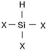


Applications Claiming Priority (2)
| Application Number | Priority Date | Filing Date | Title |
|---|---|---|---|
| US11/525,147 | 2006-09-21 | ||
| US11/525,147 US7718553B2 (en) | 2006-09-21 | 2006-09-21 | Method for forming insulation film having high density |
Publications (1)
| Publication Number | Publication Date |
|---|---|
| KR20080027138A true KR20080027138A (en) | 2008-03-26 |
Family
ID=39225514
Family Applications (1)
| Application Number | Title | Priority Date | Filing Date |
|---|---|---|---|
| KR1020070092130A Withdrawn KR20080027138A (en) | 2006-09-21 | 2007-09-11 | How to form a high density insulating film |
Country Status (2)
| Country | Link |
|---|---|
| US (1) | US7718553B2 (en) |
| KR (1) | KR20080027138A (en) |
Cited By (2)
| Publication number | Priority date | Publication date | Assignee | Title |
|---|---|---|---|---|
| KR101302592B1 (en) * | 2011-03-07 | 2013-08-30 | 한국표준과학연구원 | Process for producing silicon compound thin-film |
| KR20140143694A (en) * | 2013-06-07 | 2014-12-17 | 에이에스엠 아이피 홀딩 비.브이. | Method for filling recesses using pre-treatment with hydrocarbon-containing gas |
Families Citing this family (404)
| Publication number | Priority date | Publication date | Assignee | Title |
|---|---|---|---|---|
| US20080150028A1 (en) * | 2006-12-21 | 2008-06-26 | Advanced Micro Devices, Inc. | Zero interface polysilicon to polysilicon gate for semiconductor device |
| US7781352B2 (en) * | 2007-06-06 | 2010-08-24 | Asm Japan K.K. | Method for forming inorganic silazane-based dielectric film |
| US7651959B2 (en) | 2007-12-03 | 2010-01-26 | Asm Japan K.K. | Method for forming silazane-based dielectric film |
| US7622369B1 (en) | 2008-05-30 | 2009-11-24 | Asm Japan K.K. | Device isolation technology on semiconductor substrate |
| US10378106B2 (en) | 2008-11-14 | 2019-08-13 | Asm Ip Holding B.V. | Method of forming insulation film by modified PEALD |
| US8765233B2 (en) * | 2008-12-09 | 2014-07-01 | Asm Japan K.K. | Method for forming low-carbon CVD film for filling trenches |
| US9394608B2 (en) | 2009-04-06 | 2016-07-19 | Asm America, Inc. | Semiconductor processing reactor and components thereof |
| US7825040B1 (en) | 2009-06-22 | 2010-11-02 | Asm Japan K.K. | Method for depositing flowable material using alkoxysilane or aminosilane precursor |
| US8802201B2 (en) | 2009-08-14 | 2014-08-12 | Asm America, Inc. | Systems and methods for thin-film deposition of metal oxides using excited nitrogen-oxygen species |
| US9312155B2 (en) | 2011-06-06 | 2016-04-12 | Asm Japan K.K. | High-throughput semiconductor-processing apparatus equipped with multiple dual-chamber modules |
| US9793148B2 (en) | 2011-06-22 | 2017-10-17 | Asm Japan K.K. | Method for positioning wafers in multiple wafer transport |
| US10364496B2 (en) | 2011-06-27 | 2019-07-30 | Asm Ip Holding B.V. | Dual section module having shared and unshared mass flow controllers |
| US10854498B2 (en) | 2011-07-15 | 2020-12-01 | Asm Ip Holding B.V. | Wafer-supporting device and method for producing same |
| US20130023129A1 (en) | 2011-07-20 | 2013-01-24 | Asm America, Inc. | Pressure transmitter for a semiconductor processing environment |
| US9017481B1 (en) | 2011-10-28 | 2015-04-28 | Asm America, Inc. | Process feed management for semiconductor substrate processing |
| US8946830B2 (en) | 2012-04-04 | 2015-02-03 | Asm Ip Holdings B.V. | Metal oxide protective layer for a semiconductor device |
| US9558931B2 (en) | 2012-07-27 | 2017-01-31 | Asm Ip Holding B.V. | System and method for gas-phase sulfur passivation of a semiconductor surface |
| US9659799B2 (en) | 2012-08-28 | 2017-05-23 | Asm Ip Holding B.V. | Systems and methods for dynamic semiconductor process scheduling |
| US9021985B2 (en) | 2012-09-12 | 2015-05-05 | Asm Ip Holdings B.V. | Process gas management for an inductively-coupled plasma deposition reactor |
| US9324811B2 (en) | 2012-09-26 | 2016-04-26 | Asm Ip Holding B.V. | Structures and devices including a tensile-stressed silicon arsenic layer and methods of forming same |
| US10714315B2 (en) | 2012-10-12 | 2020-07-14 | Asm Ip Holdings B.V. | Semiconductor reaction chamber showerhead |
| US9640416B2 (en) | 2012-12-26 | 2017-05-02 | Asm Ip Holding B.V. | Single-and dual-chamber module-attachable wafer-handling chamber |
| US20160376700A1 (en) | 2013-02-01 | 2016-12-29 | Asm Ip Holding B.V. | System for treatment of deposition reactor |
| US9484191B2 (en) | 2013-03-08 | 2016-11-01 | Asm Ip Holding B.V. | Pulsed remote plasma method and system |
| US9589770B2 (en) | 2013-03-08 | 2017-03-07 | Asm Ip Holding B.V. | Method and systems for in-situ formation of intermediate reactive species |
| US8993054B2 (en) | 2013-07-12 | 2015-03-31 | Asm Ip Holding B.V. | Method and system to reduce outgassing in a reaction chamber |
| US9018111B2 (en) | 2013-07-22 | 2015-04-28 | Asm Ip Holding B.V. | Semiconductor reaction chamber with plasma capabilities |
| US9793115B2 (en) | 2013-08-14 | 2017-10-17 | Asm Ip Holding B.V. | Structures and devices including germanium-tin films and methods of forming same |
| US9240412B2 (en) | 2013-09-27 | 2016-01-19 | Asm Ip Holding B.V. | Semiconductor structure and device and methods of forming same using selective epitaxial process |
| US9556516B2 (en) | 2013-10-09 | 2017-01-31 | ASM IP Holding B.V | Method for forming Ti-containing film by PEALD using TDMAT or TDEAT |
| US10179947B2 (en) | 2013-11-26 | 2019-01-15 | Asm Ip Holding B.V. | Method for forming conformal nitrided, oxidized, or carbonized dielectric film by atomic layer deposition |
| US10683571B2 (en) | 2014-02-25 | 2020-06-16 | Asm Ip Holding B.V. | Gas supply manifold and method of supplying gases to chamber using same |
| US9447498B2 (en) | 2014-03-18 | 2016-09-20 | Asm Ip Holding B.V. | Method for performing uniform processing in gas system-sharing multiple reaction chambers |
| US10167557B2 (en) | 2014-03-18 | 2019-01-01 | Asm Ip Holding B.V. | Gas distribution system, reactor including the system, and methods of using the same |
| US11015245B2 (en) | 2014-03-19 | 2021-05-25 | Asm Ip Holding B.V. | Gas-phase reactor and system having exhaust plenum and components thereof |
| US10343907B2 (en) | 2014-03-28 | 2019-07-09 | Asm Ip Holding B.V. | Method and system for delivering hydrogen peroxide to a semiconductor processing chamber |
| US9404587B2 (en) | 2014-04-24 | 2016-08-02 | ASM IP Holding B.V | Lockout tagout for semiconductor vacuum valve |
| US9431238B2 (en) | 2014-06-05 | 2016-08-30 | Asm Ip Holding B.V. | Reactive curing process for semiconductor substrates |
| US10858737B2 (en) | 2014-07-28 | 2020-12-08 | Asm Ip Holding B.V. | Showerhead assembly and components thereof |
| US9543180B2 (en) | 2014-08-01 | 2017-01-10 | Asm Ip Holding B.V. | Apparatus and method for transporting wafers between wafer carrier and process tool under vacuum |
| US9890456B2 (en) | 2014-08-21 | 2018-02-13 | Asm Ip Holding B.V. | Method and system for in situ formation of gas-phase compounds |
| US9657845B2 (en) | 2014-10-07 | 2017-05-23 | Asm Ip Holding B.V. | Variable conductance gas distribution apparatus and method |
| US10941490B2 (en) | 2014-10-07 | 2021-03-09 | Asm Ip Holding B.V. | Multiple temperature range susceptor, assembly, reactor and system including the susceptor, and methods of using the same |
| KR102300403B1 (en) | 2014-11-19 | 2021-09-09 | 에이에스엠 아이피 홀딩 비.브이. | Method of depositing thin film |
| KR102263121B1 (en) | 2014-12-22 | 2021-06-09 | 에이에스엠 아이피 홀딩 비.브이. | Semiconductor device and manufacuring method thereof |
| KR101993070B1 (en) * | 2015-02-02 | 2019-06-25 | 가부시키가이샤 코쿠사이 엘렉트릭 | Method for manufacturing semiconductor device and recording medium |
| US9478415B2 (en) | 2015-02-13 | 2016-10-25 | Asm Ip Holding B.V. | Method for forming film having low resistance and shallow junction depth |
| US10529542B2 (en) | 2015-03-11 | 2020-01-07 | Asm Ip Holdings B.V. | Cross-flow reactor and method |
| US10276355B2 (en) | 2015-03-12 | 2019-04-30 | Asm Ip Holding B.V. | Multi-zone reactor, system including the reactor, and method of using the same |
| US10458018B2 (en) | 2015-06-26 | 2019-10-29 | Asm Ip Holding B.V. | Structures including metal carbide material, devices including the structures, and methods of forming same |
| US10600673B2 (en) | 2015-07-07 | 2020-03-24 | Asm Ip Holding B.V. | Magnetic susceptor to baseplate seal |
| US10043661B2 (en) | 2015-07-13 | 2018-08-07 | Asm Ip Holding B.V. | Method for protecting layer by forming hydrocarbon-based extremely thin film |
| US9899291B2 (en) | 2015-07-13 | 2018-02-20 | Asm Ip Holding B.V. | Method for protecting layer by forming hydrocarbon-based extremely thin film |
| US10083836B2 (en) | 2015-07-24 | 2018-09-25 | Asm Ip Holding B.V. | Formation of boron-doped titanium metal films with high work function |
| US10087525B2 (en) | 2015-08-04 | 2018-10-02 | Asm Ip Holding B.V. | Variable gap hard stop design |
| US9647114B2 (en) | 2015-08-14 | 2017-05-09 | Asm Ip Holding B.V. | Methods of forming highly p-type doped germanium tin films and structures and devices including the films |
| US9711345B2 (en) | 2015-08-25 | 2017-07-18 | Asm Ip Holding B.V. | Method for forming aluminum nitride-based film by PEALD |
| US9960072B2 (en) | 2015-09-29 | 2018-05-01 | Asm Ip Holding B.V. | Variable adjustment for precise matching of multiple chamber cavity housings |
| US9909214B2 (en) | 2015-10-15 | 2018-03-06 | Asm Ip Holding B.V. | Method for depositing dielectric film in trenches by PEALD |
| US10211308B2 (en) | 2015-10-21 | 2019-02-19 | Asm Ip Holding B.V. | NbMC layers |
| US10322384B2 (en) | 2015-11-09 | 2019-06-18 | Asm Ip Holding B.V. | Counter flow mixer for process chamber |
| US9455138B1 (en) | 2015-11-10 | 2016-09-27 | Asm Ip Holding B.V. | Method for forming dielectric film in trenches by PEALD using H-containing gas |
| US9905420B2 (en) | 2015-12-01 | 2018-02-27 | Asm Ip Holding B.V. | Methods of forming silicon germanium tin films and structures and devices including the films |
| US9607837B1 (en) | 2015-12-21 | 2017-03-28 | Asm Ip Holding B.V. | Method for forming silicon oxide cap layer for solid state diffusion process |
| US9627221B1 (en) | 2015-12-28 | 2017-04-18 | Asm Ip Holding B.V. | Continuous process incorporating atomic layer etching |
| US9735024B2 (en) | 2015-12-28 | 2017-08-15 | Asm Ip Holding B.V. | Method of atomic layer etching using functional group-containing fluorocarbon |
| US11139308B2 (en) | 2015-12-29 | 2021-10-05 | Asm Ip Holding B.V. | Atomic layer deposition of III-V compounds to form V-NAND devices |
| US9754779B1 (en) | 2016-02-19 | 2017-09-05 | Asm Ip Holding B.V. | Method for forming silicon nitride film selectively on sidewalls or flat surfaces of trenches |
| US10529554B2 (en) | 2016-02-19 | 2020-01-07 | Asm Ip Holding B.V. | Method for forming silicon nitride film selectively on sidewalls or flat surfaces of trenches |
| US10468251B2 (en) | 2016-02-19 | 2019-11-05 | Asm Ip Holding B.V. | Method for forming spacers using silicon nitride film for spacer-defined multiple patterning |
| US10501866B2 (en) | 2016-03-09 | 2019-12-10 | Asm Ip Holding B.V. | Gas distribution apparatus for improved film uniformity in an epitaxial system |
| US10343920B2 (en) | 2016-03-18 | 2019-07-09 | Asm Ip Holding B.V. | Aligned carbon nanotubes |
| US9892913B2 (en) | 2016-03-24 | 2018-02-13 | Asm Ip Holding B.V. | Radial and thickness control via biased multi-port injection settings |
| US10190213B2 (en) | 2016-04-21 | 2019-01-29 | Asm Ip Holding B.V. | Deposition of metal borides |
| US10087522B2 (en) | 2016-04-21 | 2018-10-02 | Asm Ip Holding B.V. | Deposition of metal borides |
| US10865475B2 (en) | 2016-04-21 | 2020-12-15 | Asm Ip Holding B.V. | Deposition of metal borides and silicides |
| US10367080B2 (en) | 2016-05-02 | 2019-07-30 | Asm Ip Holding B.V. | Method of forming a germanium oxynitride film |
| US10032628B2 (en) | 2016-05-02 | 2018-07-24 | Asm Ip Holding B.V. | Source/drain performance through conformal solid state doping |
| KR102592471B1 (en) | 2016-05-17 | 2023-10-20 | 에이에스엠 아이피 홀딩 비.브이. | Method of forming metal interconnection and method of fabricating semiconductor device using the same |
| US11453943B2 (en) | 2016-05-25 | 2022-09-27 | Asm Ip Holding B.V. | Method for forming carbon-containing silicon/metal oxide or nitride film by ALD using silicon precursor and hydrocarbon precursor |
| US10388509B2 (en) | 2016-06-28 | 2019-08-20 | Asm Ip Holding B.V. | Formation of epitaxial layers via dislocation filtering |
| CN105977148A (en) * | 2016-07-01 | 2016-09-28 | 深圳市华星光电技术有限公司 | Method for manufacturing insulating layer, method for manufacturing array and array substrate |
| US9859151B1 (en) | 2016-07-08 | 2018-01-02 | Asm Ip Holding B.V. | Selective film deposition method to form air gaps |
| US10612137B2 (en) | 2016-07-08 | 2020-04-07 | Asm Ip Holdings B.V. | Organic reactants for atomic layer deposition |
| US9793135B1 (en) | 2016-07-14 | 2017-10-17 | ASM IP Holding B.V | Method of cyclic dry etching using etchant film |
| US10714385B2 (en) | 2016-07-19 | 2020-07-14 | Asm Ip Holding B.V. | Selective deposition of tungsten |
| KR102354490B1 (en) | 2016-07-27 | 2022-01-21 | 에이에스엠 아이피 홀딩 비.브이. | Method of processing a substrate |
| US9812320B1 (en) | 2016-07-28 | 2017-11-07 | Asm Ip Holding B.V. | Method and apparatus for filling a gap |
| US10177025B2 (en) | 2016-07-28 | 2019-01-08 | Asm Ip Holding B.V. | Method and apparatus for filling a gap |
| US9887082B1 (en) | 2016-07-28 | 2018-02-06 | Asm Ip Holding B.V. | Method and apparatus for filling a gap |
| KR102532607B1 (en) | 2016-07-28 | 2023-05-15 | 에이에스엠 아이피 홀딩 비.브이. | Substrate processing apparatus and method of operating the same |
| US10395919B2 (en) | 2016-07-28 | 2019-08-27 | Asm Ip Holding B.V. | Method and apparatus for filling a gap |
| US10090316B2 (en) | 2016-09-01 | 2018-10-02 | Asm Ip Holding B.V. | 3D stacked multilayer semiconductor memory using doped select transistor channel |
| US10410943B2 (en) | 2016-10-13 | 2019-09-10 | Asm Ip Holding B.V. | Method for passivating a surface of a semiconductor and related systems |
| US10643826B2 (en) | 2016-10-26 | 2020-05-05 | Asm Ip Holdings B.V. | Methods for thermally calibrating reaction chambers |
| US11532757B2 (en) | 2016-10-27 | 2022-12-20 | Asm Ip Holding B.V. | Deposition of charge trapping layers |
| US10643904B2 (en) | 2016-11-01 | 2020-05-05 | Asm Ip Holdings B.V. | Methods for forming a semiconductor device and related semiconductor device structures |
| US10435790B2 (en) | 2016-11-01 | 2019-10-08 | Asm Ip Holding B.V. | Method of subatmospheric plasma-enhanced ALD using capacitively coupled electrodes with narrow gap |
| US10714350B2 (en) | 2016-11-01 | 2020-07-14 | ASM IP Holdings, B.V. | Methods for forming a transition metal niobium nitride film on a substrate by atomic layer deposition and related semiconductor device structures |
| US10229833B2 (en) | 2016-11-01 | 2019-03-12 | Asm Ip Holding B.V. | Methods for forming a transition metal nitride film on a substrate by atomic layer deposition and related semiconductor device structures |
| US10134757B2 (en) | 2016-11-07 | 2018-11-20 | Asm Ip Holding B.V. | Method of processing a substrate and a device manufactured by using the method |
| KR102546317B1 (en) | 2016-11-15 | 2023-06-21 | 에이에스엠 아이피 홀딩 비.브이. | Gas supply unit and substrate processing apparatus including the same |
| US10340135B2 (en) | 2016-11-28 | 2019-07-02 | Asm Ip Holding B.V. | Method of topologically restricted plasma-enhanced cyclic deposition of silicon or metal nitride |
| KR102762543B1 (en) | 2016-12-14 | 2025-02-05 | 에이에스엠 아이피 홀딩 비.브이. | Substrate processing apparatus |
| US11581186B2 (en) | 2016-12-15 | 2023-02-14 | Asm Ip Holding B.V. | Sequential infiltration synthesis apparatus |
| US11447861B2 (en) | 2016-12-15 | 2022-09-20 | Asm Ip Holding B.V. | Sequential infiltration synthesis apparatus and a method of forming a patterned structure |
| US9916980B1 (en) | 2016-12-15 | 2018-03-13 | Asm Ip Holding B.V. | Method of forming a structure on a substrate |
| KR102700194B1 (en) | 2016-12-19 | 2024-08-28 | 에이에스엠 아이피 홀딩 비.브이. | Substrate processing apparatus |
| US10269558B2 (en) | 2016-12-22 | 2019-04-23 | Asm Ip Holding B.V. | Method of forming a structure on a substrate |
| US10867788B2 (en) | 2016-12-28 | 2020-12-15 | Asm Ip Holding B.V. | Method of forming a structure on a substrate |
| US11390950B2 (en) | 2017-01-10 | 2022-07-19 | Asm Ip Holding B.V. | Reactor system and method to reduce residue buildup during a film deposition process |
| US10655221B2 (en) | 2017-02-09 | 2020-05-19 | Asm Ip Holding B.V. | Method for depositing oxide film by thermal ALD and PEALD |
| US10468261B2 (en) | 2017-02-15 | 2019-11-05 | Asm Ip Holding B.V. | Methods for forming a metallic film on a substrate by cyclical deposition and related semiconductor device structures |
| KR102324630B1 (en) * | 2017-03-29 | 2021-11-10 | 삼성전자주식회사 | Method of manufacturing integrated circuit device |
| US10529563B2 (en) | 2017-03-29 | 2020-01-07 | Asm Ip Holdings B.V. | Method for forming doped metal oxide films on a substrate by cyclical deposition and related semiconductor device structures |
| US10283353B2 (en) | 2017-03-29 | 2019-05-07 | Asm Ip Holding B.V. | Method of reforming insulating film deposited on substrate with recess pattern |
| US10103040B1 (en) | 2017-03-31 | 2018-10-16 | Asm Ip Holding B.V. | Apparatus and method for manufacturing a semiconductor device |
| USD830981S1 (en) | 2017-04-07 | 2018-10-16 | Asm Ip Holding B.V. | Susceptor for semiconductor substrate processing apparatus |
| KR102457289B1 (en) | 2017-04-25 | 2022-10-21 | 에이에스엠 아이피 홀딩 비.브이. | Method for depositing a thin film and manufacturing a semiconductor device |
| US10892156B2 (en) | 2017-05-08 | 2021-01-12 | Asm Ip Holding B.V. | Methods for forming a silicon nitride film on a substrate and related semiconductor device structures |
| US10446393B2 (en) | 2017-05-08 | 2019-10-15 | Asm Ip Holding B.V. | Methods for forming silicon-containing epitaxial layers and related semiconductor device structures |
| US10770286B2 (en) | 2017-05-08 | 2020-09-08 | Asm Ip Holdings B.V. | Methods for selectively forming a silicon nitride film on a substrate and related semiconductor device structures |
| US10504742B2 (en) | 2017-05-31 | 2019-12-10 | Asm Ip Holding B.V. | Method of atomic layer etching using hydrogen plasma |
| US10886123B2 (en) | 2017-06-02 | 2021-01-05 | Asm Ip Holding B.V. | Methods for forming low temperature semiconductor layers and related semiconductor device structures |
| US12040200B2 (en) | 2017-06-20 | 2024-07-16 | Asm Ip Holding B.V. | Semiconductor processing apparatus and methods for calibrating a semiconductor processing apparatus |
| US11306395B2 (en) | 2017-06-28 | 2022-04-19 | Asm Ip Holding B.V. | Methods for depositing a transition metal nitride film on a substrate by atomic layer deposition and related deposition apparatus |
| US10685834B2 (en) | 2017-07-05 | 2020-06-16 | Asm Ip Holdings B.V. | Methods for forming a silicon germanium tin layer and related semiconductor device structures |
| KR20190009245A (en) | 2017-07-18 | 2019-01-28 | 에이에스엠 아이피 홀딩 비.브이. | Methods for forming a semiconductor device structure and related semiconductor device structures |
| US11374112B2 (en) | 2017-07-19 | 2022-06-28 | Asm Ip Holding B.V. | Method for depositing a group IV semiconductor and related semiconductor device structures |
| US10541333B2 (en) | 2017-07-19 | 2020-01-21 | Asm Ip Holding B.V. | Method for depositing a group IV semiconductor and related semiconductor device structures |
| US11018002B2 (en) | 2017-07-19 | 2021-05-25 | Asm Ip Holding B.V. | Method for selectively depositing a Group IV semiconductor and related semiconductor device structures |
| US10312055B2 (en) | 2017-07-26 | 2019-06-04 | Asm Ip Holding B.V. | Method of depositing film by PEALD using negative bias |
| US10605530B2 (en) | 2017-07-26 | 2020-03-31 | Asm Ip Holding B.V. | Assembly of a liner and a flange for a vertical furnace as well as the liner and the vertical furnace |
| US10590535B2 (en) | 2017-07-26 | 2020-03-17 | Asm Ip Holdings B.V. | Chemical treatment, deposition and/or infiltration apparatus and method for using the same |
| TWI815813B (en) | 2017-08-04 | 2023-09-21 | 荷蘭商Asm智慧財產控股公司 | Showerhead assembly for distributing a gas within a reaction chamber |
| US10770336B2 (en) | 2017-08-08 | 2020-09-08 | Asm Ip Holding B.V. | Substrate lift mechanism and reactor including same |
| US10692741B2 (en) | 2017-08-08 | 2020-06-23 | Asm Ip Holdings B.V. | Radiation shield |
| US11139191B2 (en) | 2017-08-09 | 2021-10-05 | Asm Ip Holding B.V. | Storage apparatus for storing cassettes for substrates and processing apparatus equipped therewith |
| US10249524B2 (en) | 2017-08-09 | 2019-04-02 | Asm Ip Holding B.V. | Cassette holder assembly for a substrate cassette and holding member for use in such assembly |
| US11769682B2 (en) | 2017-08-09 | 2023-09-26 | Asm Ip Holding B.V. | Storage apparatus for storing cassettes for substrates and processing apparatus equipped therewith |
| US10236177B1 (en) | 2017-08-22 | 2019-03-19 | ASM IP Holding B.V.. | Methods for depositing a doped germanium tin semiconductor and related semiconductor device structures |
| USD900036S1 (en) | 2017-08-24 | 2020-10-27 | Asm Ip Holding B.V. | Heater electrical connector and adapter |
| US11830730B2 (en) | 2017-08-29 | 2023-11-28 | Asm Ip Holding B.V. | Layer forming method and apparatus |
| US11056344B2 (en) | 2017-08-30 | 2021-07-06 | Asm Ip Holding B.V. | Layer forming method |
| US11295980B2 (en) | 2017-08-30 | 2022-04-05 | Asm Ip Holding B.V. | Methods for depositing a molybdenum metal film over a dielectric surface of a substrate by a cyclical deposition process and related semiconductor device structures |
| KR102491945B1 (en) | 2017-08-30 | 2023-01-26 | 에이에스엠 아이피 홀딩 비.브이. | Substrate processing apparatus |
| KR102401446B1 (en) | 2017-08-31 | 2022-05-24 | 에이에스엠 아이피 홀딩 비.브이. | Substrate processing apparatus |
| US10607895B2 (en) | 2017-09-18 | 2020-03-31 | Asm Ip Holdings B.V. | Method for forming a semiconductor device structure comprising a gate fill metal |
| KR102630301B1 (en) | 2017-09-21 | 2024-01-29 | 에이에스엠 아이피 홀딩 비.브이. | Method of sequential infiltration synthesis treatment of infiltrateable material and structures and devices formed using same |
| US10844484B2 (en) | 2017-09-22 | 2020-11-24 | Asm Ip Holding B.V. | Apparatus for dispensing a vapor phase reactant to a reaction chamber and related methods |
| US10658205B2 (en) | 2017-09-28 | 2020-05-19 | Asm Ip Holdings B.V. | Chemical dispensing apparatus and methods for dispensing a chemical to a reaction chamber |
| US10403504B2 (en) | 2017-10-05 | 2019-09-03 | Asm Ip Holding B.V. | Method for selectively depositing a metallic film on a substrate |
| US10319588B2 (en) | 2017-10-10 | 2019-06-11 | Asm Ip Holding B.V. | Method for depositing a metal chalcogenide on a substrate by cyclical deposition |
| US10923344B2 (en) | 2017-10-30 | 2021-02-16 | Asm Ip Holding B.V. | Methods for forming a semiconductor structure and related semiconductor structures |
| US10910262B2 (en) | 2017-11-16 | 2021-02-02 | Asm Ip Holding B.V. | Method of selectively depositing a capping layer structure on a semiconductor device structure |
| KR102443047B1 (en) | 2017-11-16 | 2022-09-14 | 에이에스엠 아이피 홀딩 비.브이. | Substrate processing apparatus method and apparatus manufactured thereby |
| US11022879B2 (en) | 2017-11-24 | 2021-06-01 | Asm Ip Holding B.V. | Method of forming an enhanced unexposed photoresist layer |
| CN111344522B (en) | 2017-11-27 | 2022-04-12 | 阿斯莫Ip控股公司 | Units including clean mini environments |
| KR102597978B1 (en) | 2017-11-27 | 2023-11-06 | 에이에스엠 아이피 홀딩 비.브이. | Storage device for storing wafer cassettes for use with batch furnaces |
| US10290508B1 (en) | 2017-12-05 | 2019-05-14 | Asm Ip Holding B.V. | Method for forming vertical spacers for spacer-defined patterning |
| US10872771B2 (en) | 2018-01-16 | 2020-12-22 | Asm Ip Holding B. V. | Method for depositing a material film on a substrate within a reaction chamber by a cyclical deposition process and related device structures |
| TWI799494B (en) | 2018-01-19 | 2023-04-21 | 荷蘭商Asm 智慧財產控股公司 | Deposition method |
| WO2019142055A2 (en) | 2018-01-19 | 2019-07-25 | Asm Ip Holding B.V. | Method for depositing a gap-fill layer by plasma-assisted deposition |
| USD903477S1 (en) | 2018-01-24 | 2020-12-01 | Asm Ip Holdings B.V. | Metal clamp |
| US11018047B2 (en) | 2018-01-25 | 2021-05-25 | Asm Ip Holding B.V. | Hybrid lift pin |
| US10535516B2 (en) | 2018-02-01 | 2020-01-14 | Asm Ip Holdings B.V. | Method for depositing a semiconductor structure on a surface of a substrate and related semiconductor structures |
| USD880437S1 (en) | 2018-02-01 | 2020-04-07 | Asm Ip Holding B.V. | Gas supply plate for semiconductor manufacturing apparatus |
| US11081345B2 (en) | 2018-02-06 | 2021-08-03 | Asm Ip Holding B.V. | Method of post-deposition treatment for silicon oxide film |
| US20190249303A1 (en) * | 2018-02-09 | 2019-08-15 | Asm Ip Holding B.V. | Chemical precursors and methods for depositing a silicon oxide film on a substrate utilizing chemical precursors |
| US11685991B2 (en) | 2018-02-14 | 2023-06-27 | Asm Ip Holding B.V. | Method for depositing a ruthenium-containing film on a substrate by a cyclical deposition process |
| US10896820B2 (en) | 2018-02-14 | 2021-01-19 | Asm Ip Holding B.V. | Method for depositing a ruthenium-containing film on a substrate by a cyclical deposition process |
| US10731249B2 (en) | 2018-02-15 | 2020-08-04 | Asm Ip Holding B.V. | Method of forming a transition metal containing film on a substrate by a cyclical deposition process, a method for supplying a transition metal halide compound to a reaction chamber, and related vapor deposition apparatus |
| US10658181B2 (en) | 2018-02-20 | 2020-05-19 | Asm Ip Holding B.V. | Method of spacer-defined direct patterning in semiconductor fabrication |
| KR102636427B1 (en) | 2018-02-20 | 2024-02-13 | 에이에스엠 아이피 홀딩 비.브이. | Substrate processing method and apparatus |
| US10975470B2 (en) | 2018-02-23 | 2021-04-13 | Asm Ip Holding B.V. | Apparatus for detecting or monitoring for a chemical precursor in a high temperature environment |
| US11473195B2 (en) | 2018-03-01 | 2022-10-18 | Asm Ip Holding B.V. | Semiconductor processing apparatus and a method for processing a substrate |
| US11629406B2 (en) | 2018-03-09 | 2023-04-18 | Asm Ip Holding B.V. | Semiconductor processing apparatus comprising one or more pyrometers for measuring a temperature of a substrate during transfer of the substrate |
| US11114283B2 (en) | 2018-03-16 | 2021-09-07 | Asm Ip Holding B.V. | Reactor, system including the reactor, and methods of manufacturing and using same |
| KR102646467B1 (en) | 2018-03-27 | 2024-03-11 | 에이에스엠 아이피 홀딩 비.브이. | Method of forming an electrode on a substrate and a semiconductor device structure including an electrode |
| US11230766B2 (en) | 2018-03-29 | 2022-01-25 | Asm Ip Holding B.V. | Substrate processing apparatus and method |
| US10510536B2 (en) | 2018-03-29 | 2019-12-17 | Asm Ip Holding B.V. | Method of depositing a co-doped polysilicon film on a surface of a substrate within a reaction chamber |
| US11088002B2 (en) | 2018-03-29 | 2021-08-10 | Asm Ip Holding B.V. | Substrate rack and a substrate processing system and method |
| KR102501472B1 (en) | 2018-03-30 | 2023-02-20 | 에이에스엠 아이피 홀딩 비.브이. | Substrate processing method |
| KR102600229B1 (en) | 2018-04-09 | 2023-11-10 | 에이에스엠 아이피 홀딩 비.브이. | Substrate supporting device, substrate processing apparatus including the same and substrate processing method |
| TWI811348B (en) | 2018-05-08 | 2023-08-11 | 荷蘭商Asm 智慧財產控股公司 | Methods for depositing an oxide film on a substrate by a cyclical deposition process and related device structures |
| US12025484B2 (en) | 2018-05-08 | 2024-07-02 | Asm Ip Holding B.V. | Thin film forming method |
| US12272527B2 (en) | 2018-05-09 | 2025-04-08 | Asm Ip Holding B.V. | Apparatus for use with hydrogen radicals and method of using same |
| TWI816783B (en) | 2018-05-11 | 2023-10-01 | 荷蘭商Asm 智慧財產控股公司 | Methods for forming a doped metal carbide film on a substrate and related semiconductor device structures |
| KR102596988B1 (en) | 2018-05-28 | 2023-10-31 | 에이에스엠 아이피 홀딩 비.브이. | Method of processing a substrate and a device manufactured by the same |
| TWI840362B (en) | 2018-06-04 | 2024-05-01 | 荷蘭商Asm Ip私人控股有限公司 | Wafer handling chamber with moisture reduction |
| US11718913B2 (en) | 2018-06-04 | 2023-08-08 | Asm Ip Holding B.V. | Gas distribution system and reactor system including same |
| US11286562B2 (en) | 2018-06-08 | 2022-03-29 | Asm Ip Holding B.V. | Gas-phase chemical reactor and method of using same |
| US10797133B2 (en) | 2018-06-21 | 2020-10-06 | Asm Ip Holding B.V. | Method for depositing a phosphorus doped silicon arsenide film and related semiconductor device structures |
| KR102568797B1 (en) | 2018-06-21 | 2023-08-21 | 에이에스엠 아이피 홀딩 비.브이. | Substrate processing system |
| KR102854019B1 (en) | 2018-06-27 | 2025-09-02 | 에이에스엠 아이피 홀딩 비.브이. | Periodic deposition method for forming a metal-containing material and films and structures comprising the metal-containing material |
| TWI815915B (en) | 2018-06-27 | 2023-09-21 | 荷蘭商Asm Ip私人控股有限公司 | Cyclic deposition methods for forming metal-containing material and films and structures including the metal-containing material |
| KR102686758B1 (en) | 2018-06-29 | 2024-07-18 | 에이에스엠 아이피 홀딩 비.브이. | Method for depositing a thin film and manufacturing a semiconductor device |
| US10612136B2 (en) | 2018-06-29 | 2020-04-07 | ASM IP Holding, B.V. | Temperature-controlled flange and reactor system including same |
| US10755922B2 (en) | 2018-07-03 | 2020-08-25 | Asm Ip Holding B.V. | Method for depositing silicon-free carbon-containing film as gap-fill layer by pulse plasma-assisted deposition |
| US10388513B1 (en) | 2018-07-03 | 2019-08-20 | Asm Ip Holding B.V. | Method for depositing silicon-free carbon-containing film as gap-fill layer by pulse plasma-assisted deposition |
| US10767789B2 (en) | 2018-07-16 | 2020-09-08 | Asm Ip Holding B.V. | Diaphragm valves, valve components, and methods for forming valve components |
| US10483099B1 (en) | 2018-07-26 | 2019-11-19 | Asm Ip Holding B.V. | Method for forming thermally stable organosilicon polymer film |
| US11053591B2 (en) | 2018-08-06 | 2021-07-06 | Asm Ip Holding B.V. | Multi-port gas injection system and reactor system including same |
| US10883175B2 (en) | 2018-08-09 | 2021-01-05 | Asm Ip Holding B.V. | Vertical furnace for processing substrates and a liner for use therein |
| US10829852B2 (en) | 2018-08-16 | 2020-11-10 | Asm Ip Holding B.V. | Gas distribution device for a wafer processing apparatus |
| US11430674B2 (en) | 2018-08-22 | 2022-08-30 | Asm Ip Holding B.V. | Sensor array, apparatus for dispensing a vapor phase reactant to a reaction chamber and related methods |
| US11024523B2 (en) | 2018-09-11 | 2021-06-01 | Asm Ip Holding B.V. | Substrate processing apparatus and method |
| KR102707956B1 (en) | 2018-09-11 | 2024-09-19 | 에이에스엠 아이피 홀딩 비.브이. | Method for deposition of a thin film |
| US11049751B2 (en) | 2018-09-14 | 2021-06-29 | Asm Ip Holding B.V. | Cassette supply system to store and handle cassettes and processing apparatus equipped therewith |
| CN110970344B (en) | 2018-10-01 | 2024-10-25 | Asmip控股有限公司 | Substrate holding device, system including the same and method of using the same |
| US11232963B2 (en) | 2018-10-03 | 2022-01-25 | Asm Ip Holding B.V. | Substrate processing apparatus and method |
| KR102592699B1 (en) | 2018-10-08 | 2023-10-23 | 에이에스엠 아이피 홀딩 비.브이. | Substrate support unit and apparatuses for depositing thin film and processing the substrate including the same |
| US10847365B2 (en) | 2018-10-11 | 2020-11-24 | Asm Ip Holding B.V. | Method of forming conformal silicon carbide film by cyclic CVD |
| US10811256B2 (en) | 2018-10-16 | 2020-10-20 | Asm Ip Holding B.V. | Method for etching a carbon-containing feature |
| KR102546322B1 (en) | 2018-10-19 | 2023-06-21 | 에이에스엠 아이피 홀딩 비.브이. | Substrate processing apparatus and substrate processing method |
| KR102605121B1 (en) | 2018-10-19 | 2023-11-23 | 에이에스엠 아이피 홀딩 비.브이. | Substrate processing apparatus and substrate processing method |
| USD948463S1 (en) | 2018-10-24 | 2022-04-12 | Asm Ip Holding B.V. | Susceptor for semiconductor substrate supporting apparatus |
| US10381219B1 (en) | 2018-10-25 | 2019-08-13 | Asm Ip Holding B.V. | Methods for forming a silicon nitride film |
| US12378665B2 (en) | 2018-10-26 | 2025-08-05 | Asm Ip Holding B.V. | High temperature coatings for a preclean and etch apparatus and related methods |
| US11087997B2 (en) | 2018-10-31 | 2021-08-10 | Asm Ip Holding B.V. | Substrate processing apparatus for processing substrates |
| KR102748291B1 (en) | 2018-11-02 | 2024-12-31 | 에이에스엠 아이피 홀딩 비.브이. | Substrate support unit and substrate processing apparatus including the same |
| US11572620B2 (en) | 2018-11-06 | 2023-02-07 | Asm Ip Holding B.V. | Methods for selectively depositing an amorphous silicon film on a substrate |
| US11031242B2 (en) | 2018-11-07 | 2021-06-08 | Asm Ip Holding B.V. | Methods for depositing a boron doped silicon germanium film |
| US10847366B2 (en) | 2018-11-16 | 2020-11-24 | Asm Ip Holding B.V. | Methods for depositing a transition metal chalcogenide film on a substrate by a cyclical deposition process |
| US10818758B2 (en) | 2018-11-16 | 2020-10-27 | Asm Ip Holding B.V. | Methods for forming a metal silicate film on a substrate in a reaction chamber and related semiconductor device structures |
| US10559458B1 (en) | 2018-11-26 | 2020-02-11 | Asm Ip Holding B.V. | Method of forming oxynitride film |
| US12040199B2 (en) | 2018-11-28 | 2024-07-16 | Asm Ip Holding B.V. | Substrate processing apparatus for processing substrates |
| US11217444B2 (en) | 2018-11-30 | 2022-01-04 | Asm Ip Holding B.V. | Method for forming an ultraviolet radiation responsive metal oxide-containing film |
| KR102636428B1 (en) | 2018-12-04 | 2024-02-13 | 에이에스엠 아이피 홀딩 비.브이. | A method for cleaning a substrate processing apparatus |
| US11158513B2 (en) | 2018-12-13 | 2021-10-26 | Asm Ip Holding B.V. | Methods for forming a rhenium-containing film on a substrate by a cyclical deposition process and related semiconductor device structures |
| JP7504584B2 (en) | 2018-12-14 | 2024-06-24 | エーエスエム・アイピー・ホールディング・ベー・フェー | Method and system for forming device structures using selective deposition of gallium nitride - Patents.com |
| TWI819180B (en) | 2019-01-17 | 2023-10-21 | 荷蘭商Asm 智慧財產控股公司 | Methods of forming a transition metal containing film on a substrate by a cyclical deposition process |
| KR102727227B1 (en) | 2019-01-22 | 2024-11-07 | 에이에스엠 아이피 홀딩 비.브이. | Semiconductor processing device |
| CN111524788B (en) * | 2019-02-01 | 2023-11-24 | Asm Ip私人控股有限公司 | Method for forming topologically selective films of silicon oxide |
| TWI845607B (en) | 2019-02-20 | 2024-06-21 | 荷蘭商Asm Ip私人控股有限公司 | Cyclical deposition method and apparatus for filling a recess formed within a substrate surface |
| KR102626263B1 (en) | 2019-02-20 | 2024-01-16 | 에이에스엠 아이피 홀딩 비.브이. | Cyclical deposition method including treatment step and apparatus for same |
| JP7603377B2 (en) | 2019-02-20 | 2024-12-20 | エーエスエム・アイピー・ホールディング・ベー・フェー | Method and apparatus for filling recesses formed in a substrate surface - Patents.com |
| US11482533B2 (en) | 2019-02-20 | 2022-10-25 | Asm Ip Holding B.V. | Apparatus and methods for plug fill deposition in 3-D NAND applications |
| TWI842826B (en) | 2019-02-22 | 2024-05-21 | 荷蘭商Asm Ip私人控股有限公司 | Substrate processing apparatus and method for processing substrate |
| KR102762833B1 (en) | 2019-03-08 | 2025-02-04 | 에이에스엠 아이피 홀딩 비.브이. | STRUCTURE INCLUDING SiOCN LAYER AND METHOD OF FORMING SAME |
| KR102858005B1 (en) | 2019-03-08 | 2025-09-09 | 에이에스엠 아이피 홀딩 비.브이. | Method for Selective Deposition of Silicon Nitride Layer and Structure Including Selectively-Deposited Silicon Nitride Layer |
| KR102782593B1 (en) | 2019-03-08 | 2025-03-14 | 에이에스엠 아이피 홀딩 비.브이. | Structure Including SiOC Layer and Method of Forming Same |
| JP2020167398A (en) | 2019-03-28 | 2020-10-08 | エーエスエム・アイピー・ホールディング・ベー・フェー | Door openers and substrate processing equipment provided with door openers |
| KR102809999B1 (en) | 2019-04-01 | 2025-05-19 | 에이에스엠 아이피 홀딩 비.브이. | Method of manufacturing semiconductor device |
| KR102897355B1 (en) | 2019-04-19 | 2025-12-08 | 에이에스엠 아이피 홀딩 비.브이. | Layer forming method and apparatus |
| KR20200125453A (en) | 2019-04-24 | 2020-11-04 | 에이에스엠 아이피 홀딩 비.브이. | Gas-phase reactor system and method of using same |
| KR102869364B1 (en) | 2019-05-07 | 2025-10-10 | 에이에스엠 아이피 홀딩 비.브이. | Method for Reforming Amorphous Carbon Polymer Film |
| KR20200130121A (en) | 2019-05-07 | 2020-11-18 | 에이에스엠 아이피 홀딩 비.브이. | Chemical source vessel with dip tube |
| KR20200130652A (en) | 2019-05-10 | 2020-11-19 | 에이에스엠 아이피 홀딩 비.브이. | Method of depositing material onto a surface and structure formed according to the method |
| JP7598201B2 (en) | 2019-05-16 | 2024-12-11 | エーエスエム・アイピー・ホールディング・ベー・フェー | Wafer boat handling apparatus, vertical batch furnace and method |
| JP7612342B2 (en) | 2019-05-16 | 2025-01-14 | エーエスエム・アイピー・ホールディング・ベー・フェー | Wafer boat handling apparatus, vertical batch furnace and method |
| USD975665S1 (en) | 2019-05-17 | 2023-01-17 | Asm Ip Holding B.V. | Susceptor shaft |
| USD947913S1 (en) | 2019-05-17 | 2022-04-05 | Asm Ip Holding B.V. | Susceptor shaft |
| USD935572S1 (en) | 2019-05-24 | 2021-11-09 | Asm Ip Holding B.V. | Gas channel plate |
| USD922229S1 (en) | 2019-06-05 | 2021-06-15 | Asm Ip Holding B.V. | Device for controlling a temperature of a gas supply unit |
| KR20200141002A (en) | 2019-06-06 | 2020-12-17 | 에이에스엠 아이피 홀딩 비.브이. | Method of using a gas-phase reactor system including analyzing exhausted gas |
| US12252785B2 (en) | 2019-06-10 | 2025-03-18 | Asm Ip Holding B.V. | Method for cleaning quartz epitaxial chambers |
| KR20200143254A (en) | 2019-06-11 | 2020-12-23 | 에이에스엠 아이피 홀딩 비.브이. | Method of forming an electronic structure using an reforming gas, system for performing the method, and structure formed using the method |
| USD944946S1 (en) | 2019-06-14 | 2022-03-01 | Asm Ip Holding B.V. | Shower plate |
| USD931978S1 (en) | 2019-06-27 | 2021-09-28 | Asm Ip Holding B.V. | Showerhead vacuum transport |
| KR102911421B1 (en) | 2019-07-03 | 2026-01-12 | 에이에스엠 아이피 홀딩 비.브이. | Temperature control assembly for substrate processing apparatus and method of using same |
| JP7499079B2 (en) | 2019-07-09 | 2024-06-13 | エーエスエム・アイピー・ホールディング・ベー・フェー | Plasma device using coaxial waveguide and substrate processing method |
| KR20210008310A (en) | 2019-07-10 | 2021-01-21 | 에이에스엠 아이피 홀딩 비.브이. | Substrate supporting assembly and substrate processing apparatus comprising the same |
| KR102895115B1 (en) | 2019-07-16 | 2025-12-03 | 에이에스엠 아이피 홀딩 비.브이. | Substrate processing apparatus |
| KR102860110B1 (en) | 2019-07-17 | 2025-09-16 | 에이에스엠 아이피 홀딩 비.브이. | Methods of forming silicon germanium structures |
| KR20210010816A (en) | 2019-07-17 | 2021-01-28 | 에이에스엠 아이피 홀딩 비.브이. | Radical assist ignition plasma system and method |
| US11643724B2 (en) | 2019-07-18 | 2023-05-09 | Asm Ip Holding B.V. | Method of forming structures using a neutral beam |
| TWI839544B (en) | 2019-07-19 | 2024-04-21 | 荷蘭商Asm Ip私人控股有限公司 | Method of forming topology-controlled amorphous carbon polymer film |
| KR102903090B1 (en) | 2019-07-19 | 2025-12-19 | 에이에스엠 아이피 홀딩 비.브이. | Method of Forming Topology-Controlled Amorphous Carbon Polymer Film |
| TWI851767B (en) | 2019-07-29 | 2024-08-11 | 荷蘭商Asm Ip私人控股有限公司 | Methods for selective deposition utilizing n-type dopants and/or alternative dopants to achieve high dopant incorporation |
| CN112309900B (en) | 2019-07-30 | 2025-11-04 | Asmip私人控股有限公司 | Substrate processing equipment |
| KR20210015655A (en) | 2019-07-30 | 2021-02-10 | 에이에스엠 아이피 홀딩 비.브이. | Substrate processing apparatus and method |
| CN112309899B (en) | 2019-07-30 | 2025-11-14 | Asmip私人控股有限公司 | Substrate processing equipment |
| US11587814B2 (en) | 2019-07-31 | 2023-02-21 | Asm Ip Holding B.V. | Vertical batch furnace assembly |
| US11587815B2 (en) | 2019-07-31 | 2023-02-21 | Asm Ip Holding B.V. | Vertical batch furnace assembly |
| US11227782B2 (en) | 2019-07-31 | 2022-01-18 | Asm Ip Holding B.V. | Vertical batch furnace assembly |
| KR20210018759A (en) | 2019-08-05 | 2021-02-18 | 에이에스엠 아이피 홀딩 비.브이. | Liquid level sensor for a chemical source vessel |
| CN112342526A (en) | 2019-08-09 | 2021-02-09 | Asm Ip私人控股有限公司 | Heater assembly including cooling device and method of using same |
| USD965524S1 (en) | 2019-08-19 | 2022-10-04 | Asm Ip Holding B.V. | Susceptor support |
| USD965044S1 (en) | 2019-08-19 | 2022-09-27 | Asm Ip Holding B.V. | Susceptor shaft |
| US11639548B2 (en) | 2019-08-21 | 2023-05-02 | Asm Ip Holding B.V. | Film-forming material mixed-gas forming device and film forming device |
| USD930782S1 (en) | 2019-08-22 | 2021-09-14 | Asm Ip Holding B.V. | Gas distributor |
| USD979506S1 (en) | 2019-08-22 | 2023-02-28 | Asm Ip Holding B.V. | Insulator |
| USD949319S1 (en) | 2019-08-22 | 2022-04-19 | Asm Ip Holding B.V. | Exhaust duct |
| USD940837S1 (en) | 2019-08-22 | 2022-01-11 | Asm Ip Holding B.V. | Electrode |
| KR20210024423A (en) | 2019-08-22 | 2021-03-05 | 에이에스엠 아이피 홀딩 비.브이. | Method for forming a structure with a hole |
| US11286558B2 (en) | 2019-08-23 | 2022-03-29 | Asm Ip Holding B.V. | Methods for depositing a molybdenum nitride film on a surface of a substrate by a cyclical deposition process and related semiconductor device structures including a molybdenum nitride film |
| TWI838570B (en) | 2019-08-23 | 2024-04-11 | 荷蘭商Asm Ip私人控股有限公司 | Method for depositing silicon oxide film having improved quality by peald using bis(diethylamino)silane |
| KR102868968B1 (en) | 2019-09-03 | 2025-10-10 | 에이에스엠 아이피 홀딩 비.브이. | Methods and apparatus for depositing a chalcogenide film and structures including the film |
| KR102806450B1 (en) | 2019-09-04 | 2025-05-12 | 에이에스엠 아이피 홀딩 비.브이. | Methods for selective deposition using a sacrificial capping layer |
| KR102733104B1 (en) | 2019-09-05 | 2024-11-22 | 에이에스엠 아이피 홀딩 비.브이. | Substrate processing apparatus |
| US12469693B2 (en) | 2019-09-17 | 2025-11-11 | Asm Ip Holding B.V. | Method of forming a carbon-containing layer and structure including the layer |
| US11562901B2 (en) | 2019-09-25 | 2023-01-24 | Asm Ip Holding B.V. | Substrate processing method |
| CN112593212B (en) | 2019-10-02 | 2023-12-22 | Asm Ip私人控股有限公司 | Method for forming topologically selective silicon oxide film through cyclic plasma enhanced deposition process |
| KR20210042810A (en) | 2019-10-08 | 2021-04-20 | 에이에스엠 아이피 홀딩 비.브이. | Reactor system including a gas distribution assembly for use with activated species and method of using same |
| TWI846953B (en) | 2019-10-08 | 2024-07-01 | 荷蘭商Asm Ip私人控股有限公司 | Substrate processing device |
| TW202128273A (en) | 2019-10-08 | 2021-08-01 | 荷蘭商Asm Ip私人控股有限公司 | Gas injection system, reactor system, and method of depositing material on surface of substratewithin reaction chamber |
| TWI846966B (en) | 2019-10-10 | 2024-07-01 | 荷蘭商Asm Ip私人控股有限公司 | Method of forming a photoresist underlayer and structure including same |
| US12009241B2 (en) | 2019-10-14 | 2024-06-11 | Asm Ip Holding B.V. | Vertical batch furnace assembly with detector to detect cassette |
| TWI834919B (en) | 2019-10-16 | 2024-03-11 | 荷蘭商Asm Ip私人控股有限公司 | Method of topology-selective film formation of silicon oxide |
| US11637014B2 (en) | 2019-10-17 | 2023-04-25 | Asm Ip Holding B.V. | Methods for selective deposition of doped semiconductor material |
| KR102845724B1 (en) | 2019-10-21 | 2025-08-13 | 에이에스엠 아이피 홀딩 비.브이. | Apparatus and methods for selectively etching films |
| KR20210050453A (en) | 2019-10-25 | 2021-05-07 | 에이에스엠 아이피 홀딩 비.브이. | Methods for filling a gap feature on a substrate surface and related semiconductor structures |
| US11646205B2 (en) | 2019-10-29 | 2023-05-09 | Asm Ip Holding B.V. | Methods of selectively forming n-type doped material on a surface, systems for selectively forming n-type doped material, and structures formed using same |
| KR102890638B1 (en) | 2019-11-05 | 2025-11-25 | 에이에스엠 아이피 홀딩 비.브이. | Structures with doped semiconductor layers and methods and systems for forming same |
| US11501968B2 (en) | 2019-11-15 | 2022-11-15 | Asm Ip Holding B.V. | Method for providing a semiconductor device with silicon filled gaps |
| KR102861314B1 (en) | 2019-11-20 | 2025-09-17 | 에이에스엠 아이피 홀딩 비.브이. | Method of depositing carbon-containing material on a surface of a substrate, structure formed using the method, and system for forming the structure |
| CN112951697B (en) | 2019-11-26 | 2025-07-29 | Asmip私人控股有限公司 | Substrate processing apparatus |
| KR20210065848A (en) | 2019-11-26 | 2021-06-04 | 에이에스엠 아이피 홀딩 비.브이. | Methods for selectivley forming a target film on a substrate comprising a first dielectric surface and a second metallic surface |
| CN120432376A (en) | 2019-11-29 | 2025-08-05 | Asm Ip私人控股有限公司 | Substrate processing equipment |
| CN112885692B (en) | 2019-11-29 | 2025-08-15 | Asmip私人控股有限公司 | Substrate processing apparatus |
| JP7527928B2 (en) | 2019-12-02 | 2024-08-05 | エーエスエム・アイピー・ホールディング・ベー・フェー | Substrate processing apparatus and substrate processing method |
| KR20210070898A (en) | 2019-12-04 | 2021-06-15 | 에이에스엠 아이피 홀딩 비.브이. | Substrate processing apparatus |
| US11885013B2 (en) | 2019-12-17 | 2024-01-30 | Asm Ip Holding B.V. | Method of forming vanadium nitride layer and structure including the vanadium nitride layer |
| US11527403B2 (en) | 2019-12-19 | 2022-12-13 | Asm Ip Holding B.V. | Methods for filling a gap feature on a substrate surface and related semiconductor structures |
| KR20210089079A (en) | 2020-01-06 | 2021-07-15 | 에이에스엠 아이피 홀딩 비.브이. | Channeled lift pin |
| JP7730637B2 (en) | 2020-01-06 | 2025-08-28 | エーエスエム・アイピー・ホールディング・ベー・フェー | Gas delivery assembly, components thereof, and reactor system including same |
| US11993847B2 (en) | 2020-01-08 | 2024-05-28 | Asm Ip Holding B.V. | Injector |
| KR102882467B1 (en) | 2020-01-16 | 2025-11-05 | 에이에스엠 아이피 홀딩 비.브이. | Method of forming high aspect ratio features |
| KR102675856B1 (en) | 2020-01-20 | 2024-06-17 | 에이에스엠 아이피 홀딩 비.브이. | Method of forming thin film and method of modifying surface of thin film |
| TWI889744B (en) | 2020-01-29 | 2025-07-11 | 荷蘭商Asm Ip私人控股有限公司 | Contaminant trap system, and baffle plate stack |
| TW202513845A (en) | 2020-02-03 | 2025-04-01 | 荷蘭商Asm Ip私人控股有限公司 | Semiconductor structures and methods for forming the same |
| KR20210100010A (en) | 2020-02-04 | 2021-08-13 | 에이에스엠 아이피 홀딩 비.브이. | Method and apparatus for transmittance measurements of large articles |
| US11776846B2 (en) | 2020-02-07 | 2023-10-03 | Asm Ip Holding B.V. | Methods for depositing gap filling fluids and related systems and devices |
| TW202146691A (en) | 2020-02-13 | 2021-12-16 | 荷蘭商Asm Ip私人控股有限公司 | Gas distribution assembly, shower plate assembly, and method of adjusting conductance of gas to reaction chamber |
| CN113257655A (en) | 2020-02-13 | 2021-08-13 | Asm Ip私人控股有限公司 | Substrate processing apparatus including light receiving device and calibration method of light receiving device |
| US11781243B2 (en) | 2020-02-17 | 2023-10-10 | Asm Ip Holding B.V. | Method for depositing low temperature phosphorous-doped silicon |
| TWI895326B (en) | 2020-02-28 | 2025-09-01 | 荷蘭商Asm Ip私人控股有限公司 | System dedicated for parts cleaning |
| KR20210113043A (en) | 2020-03-04 | 2021-09-15 | 에이에스엠 아이피 홀딩 비.브이. | Alignment fixture for a reactor system |
| KR20210116249A (en) | 2020-03-11 | 2021-09-27 | 에이에스엠 아이피 홀딩 비.브이. | lockout tagout assembly and system and method of using same |
| KR20210116240A (en) | 2020-03-11 | 2021-09-27 | 에이에스엠 아이피 홀딩 비.브이. | Substrate handling device with adjustable joints |
| CN113394086A (en) | 2020-03-12 | 2021-09-14 | Asm Ip私人控股有限公司 | Method for producing a layer structure having a target topological profile |
| US12173404B2 (en) | 2020-03-17 | 2024-12-24 | Asm Ip Holding B.V. | Method of depositing epitaxial material, structure formed using the method, and system for performing the method |
| KR102755229B1 (en) | 2020-04-02 | 2025-01-14 | 에이에스엠 아이피 홀딩 비.브이. | Thin film forming method |
| TWI887376B (en) | 2020-04-03 | 2025-06-21 | 荷蘭商Asm Ip私人控股有限公司 | Method for manufacturing semiconductor device |
| TWI888525B (en) | 2020-04-08 | 2025-07-01 | 荷蘭商Asm Ip私人控股有限公司 | Apparatus and methods for selectively etching silcon oxide films |
| KR20210128343A (en) | 2020-04-15 | 2021-10-26 | 에이에스엠 아이피 홀딩 비.브이. | Method of forming chromium nitride layer and structure including the chromium nitride layer |
| US11821078B2 (en) | 2020-04-15 | 2023-11-21 | Asm Ip Holding B.V. | Method for forming precoat film and method for forming silicon-containing film |
| US11996289B2 (en) | 2020-04-16 | 2024-05-28 | Asm Ip Holding B.V. | Methods of forming structures including silicon germanium and silicon layers, devices formed using the methods, and systems for performing the methods |
| TW202143328A (en) | 2020-04-21 | 2021-11-16 | 荷蘭商Asm Ip私人控股有限公司 | Method for adjusting a film stress |
| TWI887400B (en) | 2020-04-24 | 2025-06-21 | 荷蘭商Asm Ip私人控股有限公司 | Methods and apparatus for stabilizing vanadium compounds |
| TW202208671A (en) | 2020-04-24 | 2022-03-01 | 荷蘭商Asm Ip私人控股有限公司 | Methods of forming structures including vanadium boride and vanadium phosphide layers |
| US11898243B2 (en) | 2020-04-24 | 2024-02-13 | Asm Ip Holding B.V. | Method of forming vanadium nitride-containing layer |
| KR20210132600A (en) | 2020-04-24 | 2021-11-04 | 에이에스엠 아이피 홀딩 비.브이. | Methods and systems for depositing a layer comprising vanadium, nitrogen, and a further element |
| KR102866804B1 (en) | 2020-04-24 | 2025-09-30 | 에이에스엠 아이피 홀딩 비.브이. | Vertical batch furnace assembly comprising a cooling gas supply |
| KR102783898B1 (en) | 2020-04-29 | 2025-03-18 | 에이에스엠 아이피 홀딩 비.브이. | Solid source precursor vessel |
| KR20210134869A (en) | 2020-05-01 | 2021-11-11 | 에이에스엠 아이피 홀딩 비.브이. | Fast FOUP swapping with a FOUP handler |
| JP7726664B2 (en) | 2020-05-04 | 2025-08-20 | エーエスエム・アイピー・ホールディング・ベー・フェー | Substrate processing system for processing a substrate |
| JP7736446B2 (en) | 2020-05-07 | 2025-09-09 | エーエスエム・アイピー・ホールディング・ベー・フェー | Reactor system with tuned circuit |
| KR102788543B1 (en) | 2020-05-13 | 2025-03-27 | 에이에스엠 아이피 홀딩 비.브이. | Laser alignment fixture for a reactor system |
| TW202146699A (en) | 2020-05-15 | 2021-12-16 | 荷蘭商Asm Ip私人控股有限公司 | Method of forming a silicon germanium layer, semiconductor structure, semiconductor device, method of forming a deposition layer, and deposition system |
| KR102905441B1 (en) | 2020-05-19 | 2025-12-30 | 에이에스엠 아이피 홀딩 비.브이. | Substrate processing apparatus |
| KR102795476B1 (en) | 2020-05-21 | 2025-04-11 | 에이에스엠 아이피 홀딩 비.브이. | Structures including multiple carbon layers and methods of forming and using same |
| KR20210145079A (en) | 2020-05-21 | 2021-12-01 | 에이에스엠 아이피 홀딩 비.브이. | Flange and apparatus for processing substrates |
| KR102702526B1 (en) | 2020-05-22 | 2024-09-03 | 에이에스엠 아이피 홀딩 비.브이. | Apparatus for depositing thin films using hydrogen peroxide |
| TW202212650A (en) | 2020-05-26 | 2022-04-01 | 荷蘭商Asm Ip私人控股有限公司 | Method for depositing boron and gallium containing silicon germanium layers |
| TWI876048B (en) | 2020-05-29 | 2025-03-11 | 荷蘭商Asm Ip私人控股有限公司 | Substrate processing device |
| TW202212620A (en) | 2020-06-02 | 2022-04-01 | 荷蘭商Asm Ip私人控股有限公司 | Apparatus for processing substrate, method of forming film, and method of controlling apparatus for processing substrate |
| KR20210156219A (en) | 2020-06-16 | 2021-12-24 | 에이에스엠 아이피 홀딩 비.브이. | Method for depositing boron containing silicon germanium layers |
| JP7703376B2 (en) | 2020-06-24 | 2025-07-07 | エーエスエム・アイピー・ホールディング・ベー・フェー | Method for forming a layer comprising silicon - Patent application |
| TWI873359B (en) | 2020-06-30 | 2025-02-21 | 荷蘭商Asm Ip私人控股有限公司 | Substrate processing method |
| US12431354B2 (en) | 2020-07-01 | 2025-09-30 | Asm Ip Holding B.V. | Silicon nitride and silicon oxide deposition methods using fluorine inhibitor |
| KR102707957B1 (en) | 2020-07-08 | 2024-09-19 | 에이에스엠 아이피 홀딩 비.브이. | Method for processing a substrate |
| TWI864307B (en) | 2020-07-17 | 2024-12-01 | 荷蘭商Asm Ip私人控股有限公司 | Structures, methods and systems for use in photolithography |
| KR20220011092A (en) | 2020-07-20 | 2022-01-27 | 에이에스엠 아이피 홀딩 비.브이. | Method and system for forming structures including transition metal layers |
| TWI878570B (en) | 2020-07-20 | 2025-04-01 | 荷蘭商Asm Ip私人控股有限公司 | Method and system for depositing molybdenum layers |
| TW202219303A (en) | 2020-07-27 | 2022-05-16 | 荷蘭商Asm Ip私人控股有限公司 | Thin film deposition process |
| TWI900627B (en) | 2020-08-11 | 2025-10-11 | 荷蘭商Asm Ip私人控股有限公司 | Methods for depositing a titanium aluminum carbide film structure on a substrate, gate electrode, and semiconductor deposition apparatus |
| TWI893183B (en) | 2020-08-14 | 2025-08-11 | 荷蘭商Asm Ip私人控股有限公司 | Substrate processing method |
| US12040177B2 (en) | 2020-08-18 | 2024-07-16 | Asm Ip Holding B.V. | Methods for forming a laminate film by cyclical plasma-enhanced deposition processes |
| KR20220026500A (en) | 2020-08-25 | 2022-03-04 | 에이에스엠 아이피 홀딩 비.브이. | Method of cleaning a surface |
| KR102855073B1 (en) | 2020-08-26 | 2025-09-03 | 에이에스엠 아이피 홀딩 비.브이. | Method and system for forming metal silicon oxide and metal silicon oxynitride |
| KR20220027772A (en) | 2020-08-27 | 2022-03-08 | 에이에스엠 아이피 홀딩 비.브이. | Method and system for forming patterned structures using multiple patterning process |
| TWI904232B (en) | 2020-09-10 | 2025-11-11 | 荷蘭商Asm Ip私人控股有限公司 | Methods for depositing gap filing fluids and related systems and devices |
| USD990534S1 (en) | 2020-09-11 | 2023-06-27 | Asm Ip Holding B.V. | Weighted lift pin |
| KR20220036866A (en) | 2020-09-16 | 2022-03-23 | 에이에스엠 아이피 홀딩 비.브이. | Silicon oxide deposition method |
| USD1012873S1 (en) | 2020-09-24 | 2024-01-30 | Asm Ip Holding B.V. | Electrode for semiconductor processing apparatus |
| TWI889903B (en) | 2020-09-25 | 2025-07-11 | 荷蘭商Asm Ip私人控股有限公司 | Semiconductor processing method |
| US12009224B2 (en) | 2020-09-29 | 2024-06-11 | Asm Ip Holding B.V. | Apparatus and method for etching metal nitrides |
| KR20220045900A (en) | 2020-10-06 | 2022-04-13 | 에이에스엠 아이피 홀딩 비.브이. | Deposition method and an apparatus for depositing a silicon-containing material |
| CN114293174A (en) | 2020-10-07 | 2022-04-08 | Asm Ip私人控股有限公司 | Gas supply unit and substrate processing apparatus including the same |
| TW202229613A (en) | 2020-10-14 | 2022-08-01 | 荷蘭商Asm Ip私人控股有限公司 | Method of depositing material on stepped structure |
| KR102873665B1 (en) | 2020-10-15 | 2025-10-17 | 에이에스엠 아이피 홀딩 비.브이. | Method of manufacturing semiconductor device, and substrate treatment apparatus using ether-cat |
| TW202217037A (en) | 2020-10-22 | 2022-05-01 | 荷蘭商Asm Ip私人控股有限公司 | Method of depositing vanadium metal, structure, device and a deposition assembly |
| TW202223136A (en) | 2020-10-28 | 2022-06-16 | 荷蘭商Asm Ip私人控股有限公司 | Method for forming layer on substrate, and semiconductor processing system |
| TW202229620A (en) | 2020-11-12 | 2022-08-01 | 特文特大學 | Deposition system, method for controlling reaction condition, method for depositing |
| TW202229795A (en) | 2020-11-23 | 2022-08-01 | 荷蘭商Asm Ip私人控股有限公司 | A substrate processing apparatus with an injector |
| TW202235649A (en) | 2020-11-24 | 2022-09-16 | 荷蘭商Asm Ip私人控股有限公司 | Methods for filling a gap and related systems and devices |
| TW202235675A (en) | 2020-11-30 | 2022-09-16 | 荷蘭商Asm Ip私人控股有限公司 | Injector, and substrate processing apparatus |
| US12255053B2 (en) | 2020-12-10 | 2025-03-18 | Asm Ip Holding B.V. | Methods and systems for depositing a layer |
| TW202233884A (en) | 2020-12-14 | 2022-09-01 | 荷蘭商Asm Ip私人控股有限公司 | Method of forming structures for threshold voltage control |
| US11946137B2 (en) | 2020-12-16 | 2024-04-02 | Asm Ip Holding B.V. | Runout and wobble measurement fixtures |
| TW202232639A (en) | 2020-12-18 | 2022-08-16 | 荷蘭商Asm Ip私人控股有限公司 | Wafer processing apparatus with a rotatable table |
| TW202226899A (en) | 2020-12-22 | 2022-07-01 | 荷蘭商Asm Ip私人控股有限公司 | Plasma treatment device having matching box |
| TW202242184A (en) | 2020-12-22 | 2022-11-01 | 荷蘭商Asm Ip私人控股有限公司 | Precursor capsule, precursor vessel, vapor deposition assembly, and method of loading solid precursor into precursor vessel |
| TW202231903A (en) | 2020-12-22 | 2022-08-16 | 荷蘭商Asm Ip私人控股有限公司 | Transition metal deposition method, transition metal layer, and deposition assembly for depositing transition metal on substrate |
| CN114790543A (en) * | 2021-01-26 | 2022-07-26 | Asm Ip私人控股有限公司 | Method and system for depositing layers |
| USD980814S1 (en) | 2021-05-11 | 2023-03-14 | Asm Ip Holding B.V. | Gas distributor for substrate processing apparatus |
| USD980813S1 (en) | 2021-05-11 | 2023-03-14 | Asm Ip Holding B.V. | Gas flow control plate for substrate processing apparatus |
| USD1023959S1 (en) | 2021-05-11 | 2024-04-23 | Asm Ip Holding B.V. | Electrode for substrate processing apparatus |
| USD981973S1 (en) | 2021-05-11 | 2023-03-28 | Asm Ip Holding B.V. | Reactor wall for substrate processing apparatus |
| USD990441S1 (en) | 2021-09-07 | 2023-06-27 | Asm Ip Holding B.V. | Gas flow control plate |
| USD1099184S1 (en) | 2021-11-29 | 2025-10-21 | Asm Ip Holding B.V. | Weighted lift pin |
| USD1060598S1 (en) | 2021-12-03 | 2025-02-04 | Asm Ip Holding B.V. | Split showerhead cover |
Family Cites Families (32)
| Publication number | Priority date | Publication date | Assignee | Title |
|---|---|---|---|---|
| JP2844896B2 (en) | 1990-10-17 | 1999-01-13 | 信越化学工業株式会社 | Heat resistant insulation paint |
| US5487920A (en) | 1994-04-19 | 1996-01-30 | The Boc Group, Inc. | Process for plasma-enhanced chemical vapor deposition of anti-fog and anti-scratch coatings onto various substrates |
| US5922411A (en) | 1995-07-13 | 1999-07-13 | Tonen Corporation | Composition for forming ceramic material and process for producing ceramic material |
| US6551665B1 (en) | 1997-04-17 | 2003-04-22 | Micron Technology, Inc. | Method for improving thickness uniformity of deposited ozone-TEOS silicate glass layers |
| US7354873B2 (en) | 1998-02-05 | 2008-04-08 | Asm Japan K.K. | Method for forming insulation film |
| US6784123B2 (en) | 1998-02-05 | 2004-08-31 | Asm Japan K.K. | Insulation film on semiconductor substrate and method for forming same |
| US6514880B2 (en) | 1998-02-05 | 2003-02-04 | Asm Japan K.K. | Siloxan polymer film on semiconductor substrate and method for forming same |
| US20060258176A1 (en) | 1998-02-05 | 2006-11-16 | Asm Japan K.K. | Method for forming insulation film |
| US6881683B2 (en) | 1998-02-05 | 2005-04-19 | Asm Japan K.K. | Insulation film on semiconductor substrate and method for forming same |
| US6383955B1 (en) | 1998-02-05 | 2002-05-07 | Asm Japan K.K. | Silicone polymer insulation film on semiconductor substrate and method for forming the film |
| US7064088B2 (en) | 1998-02-05 | 2006-06-20 | Asm Japan K.K. | Method for forming low-k hard film |
| US6432846B1 (en) | 1999-02-02 | 2002-08-13 | Asm Japan K.K. | Silicone polymer insulation film on semiconductor substrate and method for forming the film |
| TW437017B (en) | 1998-02-05 | 2001-05-28 | Asm Japan Kk | Silicone polymer insulation film on semiconductor substrate and method for formation thereof |
| US7582575B2 (en) | 1998-02-05 | 2009-09-01 | Asm Japan K.K. | Method for forming insulation film |
| US6541367B1 (en) | 2000-01-18 | 2003-04-01 | Applied Materials, Inc. | Very low dielectric constant plasma-enhanced CVD films |
| WO2002017374A1 (en) | 2000-08-18 | 2002-02-28 | Tokyo Electron Limited | Low-dielectric silicon nitride film and method of forming the same, semiconductor device and fabrication process thereof |
| US6436822B1 (en) | 2000-11-20 | 2002-08-20 | Intel Corporation | Method for making a carbon doped oxide dielectric material |
| SG98468A1 (en) | 2001-01-17 | 2003-09-19 | Air Prod & Chem | Organosilicon precursors for interlayer dielectric films with low dielectric constants |
| US6403486B1 (en) | 2001-04-30 | 2002-06-11 | Taiwan Semiconductor Manufacturing Company | Method for forming a shallow trench isolation |
| JP3778045B2 (en) | 2001-10-09 | 2006-05-24 | 三菱電機株式会社 | Manufacturing method of low dielectric constant material, low dielectric constant material, insulating film and semiconductor device using the low dielectric constant material |
| US6818570B2 (en) | 2002-03-04 | 2004-11-16 | Asm Japan K.K. | Method of forming silicon-containing insulation film having low dielectric constant and high mechanical strength |
| US6815373B2 (en) | 2002-04-16 | 2004-11-09 | Applied Materials Inc. | Use of cyclic siloxanes for hardness improvement of low k dielectric films |
| US20040137757A1 (en) | 2003-01-13 | 2004-07-15 | Applied Materials, Inc. | Method and apparatus to improve cracking thresholds and mechanical properties of low-k dielectric material |
| US6740602B1 (en) | 2003-03-17 | 2004-05-25 | Asm Japan K.K. | Method of forming low-dielectric constant film on semiconductor substrate by plasma reaction using high-RF power |
| US6835664B1 (en) | 2003-06-26 | 2004-12-28 | Micron Technology, Inc. | Methods of forming trenched isolation regions |
| US20050129932A1 (en) | 2003-12-16 | 2005-06-16 | Briley Robert E. | Rivet and coating technique |
| US7129187B2 (en) | 2004-07-14 | 2006-10-31 | Tokyo Electron Limited | Low-temperature plasma-enhanced chemical vapor deposition of silicon-nitrogen-containing films |
| JP2006054353A (en) | 2004-08-13 | 2006-02-23 | Az Electronic Materials Kk | Siliceous film with little flat band shift and its production method |
| US7268057B2 (en) | 2005-03-30 | 2007-09-11 | Micron Technology, Inc. | Methods of filling openings with oxide, and methods of forming trenched isolation regions |
| US20070065597A1 (en) | 2005-09-15 | 2007-03-22 | Asm Japan K.K. | Plasma CVD film formation apparatus provided with mask |
| US20070289534A1 (en) | 2006-05-30 | 2007-12-20 | Applied Materials, Inc. | Process chamber for dielectric gapfill |
| US7781352B2 (en) | 2007-06-06 | 2010-08-24 | Asm Japan K.K. | Method for forming inorganic silazane-based dielectric film |
-
2006
- 2006-09-21 US US11/525,147 patent/US7718553B2/en active Active
-
2007
- 2007-09-11 KR KR1020070092130A patent/KR20080027138A/en not_active Withdrawn
Cited By (2)
| Publication number | Priority date | Publication date | Assignee | Title |
|---|---|---|---|---|
| KR101302592B1 (en) * | 2011-03-07 | 2013-08-30 | 한국표준과학연구원 | Process for producing silicon compound thin-film |
| KR20140143694A (en) * | 2013-06-07 | 2014-12-17 | 에이에스엠 아이피 홀딩 비.브이. | Method for filling recesses using pre-treatment with hydrocarbon-containing gas |
Also Published As
| Publication number | Publication date |
|---|---|
| US20080076266A1 (en) | 2008-03-27 |
| US7718553B2 (en) | 2010-05-18 |
Similar Documents
| Publication | Publication Date | Title |
|---|---|---|
| KR20080027138A (en) | How to form a high density insulating film | |
| US7781352B2 (en) | Method for forming inorganic silazane-based dielectric film | |
| US7651959B2 (en) | Method for forming silazane-based dielectric film | |
| US6991959B2 (en) | Method of manufacturing silicon carbide film | |
| US9018108B2 (en) | Low shrinkage dielectric films | |
| US7354873B2 (en) | Method for forming insulation film | |
| US9029272B1 (en) | Method for treating SiOCH film with hydrogen plasma | |
| US6919270B2 (en) | Method of manufacturing silicon carbide film | |
| US8889566B2 (en) | Low cost flowable dielectric films | |
| US7312524B2 (en) | Method for fabricating an ultralow dielectric constant material as an intralevel or interlevel dielectric in a semiconductor device and electronic device made | |
| CN103154102A (en) | Amine curing silicon-nitride-hydride films | |
| CN102754193A (en) | Flowable dielectric using oxide liner | |
| JP2015521375A (en) | Improved densification for flowable membranes | |
| CN102668045A (en) | Oxygen-doping for non-carbon radical-component cvd films | |
| KR20130135301A (en) | Radical vapor chemical vapor deposition | |
| KR20010072415A (en) | Method and apparatus for forming a film on a substrate | |
| JP2016096331A (en) | Improvement of depth of cure penetration and stress adjustment of flowable membrane | |
| JP7723734B2 (en) | Systems and methods for depositing low-κ dielectric films | |
| US20060258176A1 (en) | Method for forming insulation film | |
| KR102453724B1 (en) | Improved step coverage dielectric | |
| JP4117768B2 (en) | Siloxane polymer film on semiconductor substrate and method for producing the same | |
| JP2006173235A (en) | Method for forming insulating layer, heat treatment device, and storage medium |
Legal Events
| Date | Code | Title | Description |
|---|---|---|---|
| PA0109 | Patent application |
St.27 status event code: A-0-1-A10-A12-nap-PA0109 |
|
| PG1501 | Laying open of application |
St.27 status event code: A-1-1-Q10-Q12-nap-PG1501 |
|
| PC1203 | Withdrawal of no request for examination |
St.27 status event code: N-1-6-B10-B12-nap-PC1203 |
|
| WITN | Application deemed withdrawn, e.g. because no request for examination was filed or no examination fee was paid | ||
| P22-X000 | Classification modified |
St.27 status event code: A-2-2-P10-P22-nap-X000 |
|
| P22-X000 | Classification modified |
St.27 status event code: A-2-2-P10-P22-nap-X000 |