KR20070078885A - Liquid crystal display panel and bidirectional liquid crystal display including the same - Google Patents
Liquid crystal display panel and bidirectional liquid crystal display including the same Download PDFInfo
- Publication number
- KR20070078885A KR20070078885A KR1020060009299A KR20060009299A KR20070078885A KR 20070078885 A KR20070078885 A KR 20070078885A KR 1020060009299 A KR1020060009299 A KR 1020060009299A KR 20060009299 A KR20060009299 A KR 20060009299A KR 20070078885 A KR20070078885 A KR 20070078885A
- Authority
- KR
- South Korea
- Prior art keywords
- liquid crystal
- crystal display
- display panel
- display area
- color filter
- Prior art date
- Legal status (The legal status is an assumption and is not a legal conclusion. Google has not performed a legal analysis and makes no representation as to the accuracy of the status listed.)
- Withdrawn
Links
Images


Classifications
-
- G—PHYSICS
- G02—OPTICS
- G02F—OPTICAL DEVICES OR ARRANGEMENTS FOR THE CONTROL OF LIGHT BY MODIFICATION OF THE OPTICAL PROPERTIES OF THE MEDIA OF THE ELEMENTS INVOLVED THEREIN; NON-LINEAR OPTICS; FREQUENCY-CHANGING OF LIGHT; OPTICAL LOGIC ELEMENTS; OPTICAL ANALOGUE/DIGITAL CONVERTERS
- G02F1/00—Devices or arrangements for the control of the intensity, colour, phase, polarisation or direction of light arriving from an independent light source, e.g. switching, gating or modulating; Non-linear optics
- G02F1/01—Devices or arrangements for the control of the intensity, colour, phase, polarisation or direction of light arriving from an independent light source, e.g. switching, gating or modulating; Non-linear optics for the control of the intensity, phase, polarisation or colour
- G02F1/13—Devices or arrangements for the control of the intensity, colour, phase, polarisation or direction of light arriving from an independent light source, e.g. switching, gating or modulating; Non-linear optics for the control of the intensity, phase, polarisation or colour based on liquid crystals, e.g. single liquid crystal display cells
- G02F1/133—Constructional arrangements; Operation of liquid crystal cells; Circuit arrangements
- G02F1/1333—Constructional arrangements; Manufacturing methods
- G02F1/1335—Structural association of cells with optical devices, e.g. polarisers or reflectors
- G02F1/133509—Filters, e.g. light shielding masks
- G02F1/133514—Colour filters
-
- G—PHYSICS
- G02—OPTICS
- G02F—OPTICAL DEVICES OR ARRANGEMENTS FOR THE CONTROL OF LIGHT BY MODIFICATION OF THE OPTICAL PROPERTIES OF THE MEDIA OF THE ELEMENTS INVOLVED THEREIN; NON-LINEAR OPTICS; FREQUENCY-CHANGING OF LIGHT; OPTICAL LOGIC ELEMENTS; OPTICAL ANALOGUE/DIGITAL CONVERTERS
- G02F1/00—Devices or arrangements for the control of the intensity, colour, phase, polarisation or direction of light arriving from an independent light source, e.g. switching, gating or modulating; Non-linear optics
- G02F1/01—Devices or arrangements for the control of the intensity, colour, phase, polarisation or direction of light arriving from an independent light source, e.g. switching, gating or modulating; Non-linear optics for the control of the intensity, phase, polarisation or colour
- G02F1/13—Devices or arrangements for the control of the intensity, colour, phase, polarisation or direction of light arriving from an independent light source, e.g. switching, gating or modulating; Non-linear optics for the control of the intensity, phase, polarisation or colour based on liquid crystals, e.g. single liquid crystal display cells
- G02F1/133—Constructional arrangements; Operation of liquid crystal cells; Circuit arrangements
- G02F1/1333—Constructional arrangements; Manufacturing methods
- G02F1/1335—Structural association of cells with optical devices, e.g. polarisers or reflectors
- G02F1/133524—Light-guides, e.g. fibre-optic bundles, louvered or jalousie light-guides
-
- G—PHYSICS
- G02—OPTICS
- G02F—OPTICAL DEVICES OR ARRANGEMENTS FOR THE CONTROL OF LIGHT BY MODIFICATION OF THE OPTICAL PROPERTIES OF THE MEDIA OF THE ELEMENTS INVOLVED THEREIN; NON-LINEAR OPTICS; FREQUENCY-CHANGING OF LIGHT; OPTICAL LOGIC ELEMENTS; OPTICAL ANALOGUE/DIGITAL CONVERTERS
- G02F1/00—Devices or arrangements for the control of the intensity, colour, phase, polarisation or direction of light arriving from an independent light source, e.g. switching, gating or modulating; Non-linear optics
- G02F1/01—Devices or arrangements for the control of the intensity, colour, phase, polarisation or direction of light arriving from an independent light source, e.g. switching, gating or modulating; Non-linear optics for the control of the intensity, phase, polarisation or colour
- G02F1/13—Devices or arrangements for the control of the intensity, colour, phase, polarisation or direction of light arriving from an independent light source, e.g. switching, gating or modulating; Non-linear optics for the control of the intensity, phase, polarisation or colour based on liquid crystals, e.g. single liquid crystal display cells
- G02F1/133—Constructional arrangements; Operation of liquid crystal cells; Circuit arrangements
- G02F1/1333—Constructional arrangements; Manufacturing methods
- G02F1/1335—Structural association of cells with optical devices, e.g. polarisers or reflectors
- G02F1/133528—Polarisers
- G02F1/133536—Reflective polarizers
-
- G—PHYSICS
- G02—OPTICS
- G02F—OPTICAL DEVICES OR ARRANGEMENTS FOR THE CONTROL OF LIGHT BY MODIFICATION OF THE OPTICAL PROPERTIES OF THE MEDIA OF THE ELEMENTS INVOLVED THEREIN; NON-LINEAR OPTICS; FREQUENCY-CHANGING OF LIGHT; OPTICAL LOGIC ELEMENTS; OPTICAL ANALOGUE/DIGITAL CONVERTERS
- G02F1/00—Devices or arrangements for the control of the intensity, colour, phase, polarisation or direction of light arriving from an independent light source, e.g. switching, gating or modulating; Non-linear optics
- G02F1/01—Devices or arrangements for the control of the intensity, colour, phase, polarisation or direction of light arriving from an independent light source, e.g. switching, gating or modulating; Non-linear optics for the control of the intensity, phase, polarisation or colour
- G02F1/13—Devices or arrangements for the control of the intensity, colour, phase, polarisation or direction of light arriving from an independent light source, e.g. switching, gating or modulating; Non-linear optics for the control of the intensity, phase, polarisation or colour based on liquid crystals, e.g. single liquid crystal display cells
- G02F1/133—Constructional arrangements; Operation of liquid crystal cells; Circuit arrangements
- G02F1/1333—Constructional arrangements; Manufacturing methods
- G02F1/1335—Structural association of cells with optical devices, e.g. polarisers or reflectors
- G02F1/133553—Reflecting elements
- G02F1/133555—Transflectors
-
- G—PHYSICS
- G09—EDUCATION; CRYPTOGRAPHY; DISPLAY; ADVERTISING; SEALS
- G09G—ARRANGEMENTS OR CIRCUITS FOR CONTROL OF INDICATING DEVICES USING STATIC MEANS TO PRESENT VARIABLE INFORMATION
- G09G3/00—Control arrangements or circuits, of interest only in connection with visual indicators other than cathode-ray tubes
- G09G3/20—Control arrangements or circuits, of interest only in connection with visual indicators other than cathode-ray tubes for presentation of an assembly of a number of characters, e.g. a page, by composing the assembly by combination of individual elements arranged in a matrix no fixed position being assigned to or needed to be assigned to the individual characters or partial characters
- G09G3/34—Control arrangements or circuits, of interest only in connection with visual indicators other than cathode-ray tubes for presentation of an assembly of a number of characters, e.g. a page, by composing the assembly by combination of individual elements arranged in a matrix no fixed position being assigned to or needed to be assigned to the individual characters or partial characters by control of light from an independent source
- G09G3/3406—Control of illumination source
Landscapes
- Physics & Mathematics (AREA)
- Nonlinear Science (AREA)
- Mathematical Physics (AREA)
- Chemical & Material Sciences (AREA)
- Crystallography & Structural Chemistry (AREA)
- General Physics & Mathematics (AREA)
- Optics & Photonics (AREA)
- Liquid Crystal (AREA)
Abstract
본 발명은 양방향 액정 표시 패널 및 이를 포함하는 양방향 액정 표시 장치에 관한 것이다. 본 발명은 메인 화면 영역에 투과형 편광판을 사용하고, 서브 화면 영역에 반사형 편광판을 사용함으로서, 박막 트랜지스터 기판 및 컬러 필터 기판 전체를 투과형으로 제작하여 광 투과율을 높여 액정 표시 패널의 전체적인 광학 특성을 높일 수 있다. 또한, 본 발명은 컬러 필터 기판의 전체 영역을 투과형으로 제작하므로 제작공정이 쉽고 공정수가 감소하여 원가 부담을 최소화할 수 있다. 더욱이, 본 발명은 도광판을 메인 화면 영역뿐만 아니라 서브 화면 영역까지 형성하여 어두운 곳에서도 서브 화면 영역이 잘 보이는 액정 표시 장치를 제공할 수 있다.The present invention relates to a bidirectional liquid crystal display panel and a bidirectional liquid crystal display including the same. According to the present invention, a transmissive polarizer is used in the main screen area and a reflective polarizer is used in the sub screen area. Thus, the entire thin film transistor substrate and the color filter substrate are manufactured in a transmissive type to increase light transmittance, thereby improving overall optical characteristics of the liquid crystal display panel. Can be. In addition, since the present invention manufactures the entire area of the color filter substrate in a transmissive type, the manufacturing process is easy and the number of processes is reduced, thereby minimizing the cost burden. In addition, the present invention can provide a liquid crystal display device in which the light guide plate is formed not only in the main screen area but also in the sub screen area so that the sub screen area is easily seen even in the dark.
Description
도 1은 본 발명에 따른 양면 액정 표시 패널의 분해 사시도.1 is an exploded perspective view of a double-sided liquid crystal display panel according to the present invention.
도 2는 본 발명에 따른 양면 액정 표시 패널을 설명하기 위한 평면도.2 is a plan view for explaining a double-sided liquid crystal display panel according to the present invention.
도 3은 도 2의 C영역을 확대 도시한 개념도.3 is an enlarged conceptual view illustrating region C of FIG. 2.
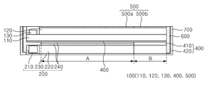
도 4는 본 발명의 제 1 실시예에 따른 양면 액정 표시 장치의 분해 사시도.4 is an exploded perspective view of a double-sided liquid crystal display according to a first embodiment of the present invention.
도 5는 도 4의 A-A선에서 취한 단면도.FIG. 5 is a sectional view taken on line A-A in FIG. 4; FIG.
도 6은 본 발명의 제 2 실시예에 따른 양면 액정 표시 장치의 분해 사시도.6 is an exploded perspective view of a double-sided liquid crystal display according to a second embodiment of the present invention.
도 7은 도 6의 B-B선에서 취한 단면도.FIG. 7 is a sectional view taken on line B-B in FIG. 6; FIG.
<도면의 주요 부분에 대한 부호의 설명><Explanation of symbols for the main parts of the drawings>
100: 액정 표시 패널 110: 박막 트랜지스터 기판100 liquid
120: 컬러 필러 기판 130: 구동 IC120: color filler substrate 130: drive IC
210: 광원 220: 도광판210: light source 220: light guide plate
230: 반사판 240: 광학 시트230: reflector 240: optical sheet
200: 백라이트부 500a: 제 1 편광판200:
500b: 제 2 편광판 400: 제 3 편광판500b: second polarizing plate 400: third polarizing plate
본 발명은 양방향 액정 표시 패널 및 이를 포함하는 양방향 액정 표시 장치에 관한 것으로, 특히 투과형 편광판과 반사형 편광판을 사용한 양방향 액정 표시 패널 및 이를 포함하는 양방향 액정 표시 장치에 관한 것이다.The present invention relates to a bidirectional liquid crystal display panel and a bidirectional liquid crystal display device including the same, and more particularly, to a bidirectional liquid crystal display panel using a transmissive polarizing plate and a reflective polarizing plate, and a bidirectional liquid crystal display including the same.
양쪽 면에서 화상을 볼 수 있는 양면 액정 표시 장치는 최근 폴더형 휴대용 무선 단말기에 적용되어 폴더를 닫았을 경우와 열었을 경우에 상관없이 정보를 표시할 수 있도록 한다.A double-sided liquid crystal display device that can view images on both sides has recently been applied to a foldable portable wireless terminal so that information can be displayed regardless of whether the folder is closed or opened.
이러한 종래의 양면 액정 표시 장치의 경우, 일면 방향으로 화상을 표시하는 메인 화면 영역과 타면 방향으로 화상을 표시하는 서브 화면 영역을 포함하는 액정 표시 패널과, 상기 액정 표시 패널에 광을 공급하기 위한 백라이트를 포함한다. 이때, 상기 액정 표시 패널은 박막 트랜지스터 및 컬러 필터 기판과, 상기 두 기판의 양면에 부착된 편광판을 포함한다.In the conventional double-sided liquid crystal display device, a liquid crystal display panel including a main screen area displaying an image in one direction and a sub screen area displaying an image in the other direction, and a backlight for supplying light to the liquid crystal display panel. It includes. In this case, the liquid crystal display panel includes a thin film transistor and a color filter substrate, and polarizers attached to both surfaces of the two substrates.
상기와 같은 구조의 종래 기술에 따른 양면 액정 표시 장치는 하나의 패널로 메인 화면과 서브 화면을 구동하기 위해 컬러 필터 기판과 상기 컬러 필터 기판 상에 부착된 편광판을 반투과형으로 제작한다.The double-sided liquid crystal display device according to the related art having the above structure manufactures a color filter substrate and a polarizer attached to the color filter substrate in a semi-transmissive manner to drive the main screen and the sub screen with one panel.
따라서, 투과모드의 화면을 형성하는 메인 화면 영역에도 반투과 액정 및 편광판을 적용하는 불합리가 발생하고, 서브 화면 영역의 컬러 필터 기판에 반투과 공정 실시에 의한 공정 수 증가에 따른 원가 부담이 늘어나는 문제점이 있다.Therefore, irrationality of applying the transflective liquid crystal and the polarizing plate also occurs in the main screen area forming the transmissive mode screen, and the cost burden increases due to the increase in the number of processes by performing the transflective process on the color filter substrate in the sub screen area. There is this.
본 발명의 목적은 전술된 종래 기술의 문제점을 해결하기 위한 것으로서, 액정 표시 패널의 메인 화면 영역과 서브 화면 영역이 투과형으로 제작된 양방향 액정 표시 패널 및 이를 포함하는 양방향 액정 표시 장치를 제공하는 것이다.SUMMARY OF THE INVENTION An object of the present invention is to solve the above-described problems of the prior art, and to provide a bidirectional liquid crystal display panel including a main screen region and a sub screen region of a liquid crystal display panel formed in a transmissive type and a bidirectional liquid crystal display device including the same.
본 발명의 다른 목적은 어두운 곳에서도 서브 디스플레이 영역이 보이는 양방향 액정 표시 패널 및 이를 포함하는 양방향 액정 표시 장치를 제공하는 것이다.Another object of the present invention is to provide a bidirectional liquid crystal display panel having a sub display area visible in a dark place and a bidirectional liquid crystal display device including the same.
상기의 목적을 달성하기 위해 본 발명은 제 1 표시 영역과 제 2 표시 영역이 정의된 박막 트랜지스터 기판 및 컬러 필터 기판을 포함하는 액정 표시 패널로서, 상기 컬러 필터 기판의 일 면에 마련되고 상기 제 1 표시 영역에 마련된 제 1 편광판 및 상기 제 2 표시 영역에 마련된 제 2 편광판을 포함하는 것을 특징으로 하는 액정 표시 패널을 제공한다.In order to achieve the above object, the present invention provides a liquid crystal display panel including a thin film transistor substrate and a color filter substrate in which a first display region and a second display region are defined. A liquid crystal display panel comprising a first polarizing plate provided in a display area and a second polarizing plate provided in the second display area.
이때, 상기 제 1 편광판은 투과형일 수 있으며, 상기 제 2 편광판은 반사형일 수 있다.In this case, the first polarizing plate may be a transmission type, and the second polarizing plate may be a reflection type.
또한, 상기 컬러 필터 기판은 투과형일 수 있고, 상기 제 2 표시 영역은 서브 화면 표시 영역일 수 있다.The color filter substrate may be a transmissive type, and the second display area may be a sub screen display area.
상기 컬러 필터 기판의 제 1 표시 영역은 단일 화소 각각이 적색, 녹색, 청색의 서브 픽셀을 포함할 수 있다.In the first display area of the color filter substrate, each single pixel may include red, green, and blue subpixels.
상기 컬러 필터 기판의 제 2 표시 영역은 단일 화소에 적색, 녹색, 청색 중 어느 하나의 서브 픽셀을 포함할 수 있다.The second display area of the color filter substrate may include any one of red, green, and blue subpixels in a single pixel.
더욱이, 본 발명은 제 1 표시 영역과 제 2 표시 영역이 정의된 박막 트랜지스터 기판 및 컬러 필터 기판을 포함하는 액정 표시 패널로서, 상기 컬러 필터 기판의 일 면에 마련되고 제 1 표시 영역에 마련된 제 1 편광판 및 제 2 표시 영역에 마련되고 반사형 편광판인 제 2 편광판을 포함하는 액정 표시 패널과, 상기 액정 표시 패널에 광을 공급하기 위한 백라이트부를 포함하는 것을 특징으로 하는 액정 표시 장치를 제공할 수 있다.Furthermore, the present invention is a liquid crystal display panel including a thin film transistor substrate and a color filter substrate in which a first display region and a second display region are defined, the first display region being provided on one surface of the color filter substrate and provided in the first display region. A liquid crystal display panel comprising a polarizing plate and a second polarizing plate provided in the second display area and a reflective polarizing plate, and a backlight unit for supplying light to the liquid crystal display panel may be provided. .
이때, 상기 백라이트부는 도광판과 광원을 포함하고, 상기 도광판은 액정 표시 패널 하부의 제 1 표시 영역에 마련될 수 있다.In this case, the backlight unit may include a light guide plate and a light source, and the light guide plate may be provided in the first display area under the liquid crystal display panel.
또한, 상기 백라이트부는 도광판과 광원을 포함하고, 상기 도광판은 액정 표시 패널 하부의 제 1 및 제 2 표시 영역에 마련될 수 있다.The backlight unit may include a light guide plate and a light source, and the light guide plate may be provided in the first and second display areas under the liquid crystal display panel.
이하, 첨부된 도면을 참조하여 본 발명의 실시예를 더욱 상세히 설명한다. 그러나 본 발명은 이하에서 개시되는 실시예에 한정되는 것이 아니라 서로 다른 다양한 형태로 구현될 것이며, 단지 본 실시예들은 본 발명의 개시가 완전하도록 하며, 통상의 지식을 가진 자에게 발명의 범주를 완전하게 알려주기 위해 제공되는 것이다.Hereinafter, with reference to the accompanying drawings will be described an embodiment of the present invention in more detail. However, the present invention is not limited to the embodiments disclosed below, but will be implemented in various forms, and only the embodiments are intended to complete the disclosure of the present invention, and to those skilled in the art to fully understand the scope of the invention. It is provided to inform you.
도면에서 여러 층 및 각 영역을 명확하게 표현하기 위하여 두께를 확대하여 표현하였으며 도면상에서 동일 부호는 동일한 요소를 지칭하도록 하였다. 또한, 층, 막, 영역, 판 등의 부분이 다른 부분 상부에 또는 위에 있다고 표현되는 경우는 각 부분이 다른 부분의 바로 상부 또는 바로 위에 있는 경우뿐만 아니라 각 부분과 다른 부분의 사이에 또 다른 부분이 있는 경우도 포함한다.In the drawings, the thickness of layers, films, panels, regions, etc., may be exaggerated for clarity, and like reference numerals designate like elements. In addition, when a part such as a layer, a film, an area, or a plate is expressed as being on or above another part, not only when each part is directly above or directly above the other part but also another part between each part and another part This includes cases.
도 1은 본 발명에 따른 양면 액정 표시 패널의 분해 사시도이고, 도 2는 본 발명에 따른 액정 표시 패널을 설명하기 위한 평면도이고, 도 3은 도 2의 C 영역을 확대 도시한 개념도이다.1 is an exploded perspective view of a double-sided liquid crystal display panel according to the present invention, FIG. 2 is a plan view illustrating a liquid crystal display panel according to the present invention, and FIG. 3 is an enlarged conceptual view of region C of FIG. 2.
도 1 내지 도 3을 참조하면, 본 발명에 따른 양면 액정 표시 패널은 메인 디스플레이인 메인 표시 영역(A)과 서브 디스플레이인 섹션 표시 영역(B)을 갖는 박막 트랜지스터 기판(110) 및 컬러 필터 기판(120)을 포함한다. 이때, 상기 박막 트랜지스터 기판(110) 및 컬러 필터 기판(120)의 양면에 마련된 편광판(400, 500)을 포함한다. 또한, 상기 박막 트랜지스터 기판(110)과 컬러 필터 기판(120) 사이에 마련된 액정층(미도시)을 포함한다.1 to 3, a double-sided liquid crystal display panel according to an exemplary embodiment of the present invention includes a thin
상기 박막 트랜지스터 기판(110)은 매트릭스 형태의 복수의 화소 영역이 정의되고, 상기 화소 영역 내에 마련된 박막 트랜지스터와 화소 전극을 포함하는 투광성의 절연 기판인 것이 바람직하다. 이때, 상기 박막 트랜지스터와 화소 전극을 형성하기 위한 절연 기판으로는 도면에서와 같이 직사각형 형상의 유리 기판을 사용하는 것이 효과적이다.The thin
상기의 박막 트랜지스터들의 소스 단자는 일 방향으로 뻗은 데이터 라인에 접속되고, 게이트 단자는 상기 일 방향과 직교하는 타 방향으로 뻗은 게이트 라인에 연결된다. 드레인 단자는 상기 화소 영역의 일부에 마련된 투명한 도전성 재질인 화소 전극과 접속된다. 이때, 투명 도전성 재질로는 인듐 틴 옥사이드(Indium Tin Oxide, ITO) 또는 인듐 징크 옥사이드(Indium Zinc Oxide, IZO)를 사용하는 것 이 바람직하다.The source terminal of the thin film transistors is connected to a data line extending in one direction, and the gate terminal is connected to a gate line extending in another direction perpendicular to the one direction. The drain terminal is connected to a pixel electrode made of a transparent conductive material provided in a part of the pixel region. In this case, it is preferable to use indium tin oxide (ITO) or indium zinc oxide (IZO) as the transparent conductive material.
이러한 박막 트랜지스터 기판(110)은 게이트 라인과 데이터 라인에 전기적 신호를 인가하면 박막 트랜지스터가 턴-온(turn-on) 또는 턴-오프(turn-off)되어 데이터 라인의 전기적 신호 즉, 화소 형성에 필요한 전기적 신호를 화소 전극에 인가한다.When the thin
이를 위해 상기 게이트 라인 및 데이터 라인을 구동하기 위한 별도의 구동부(130)를 더 포함한다. 이때, 본 발명에 따른 액정 표시 패널은 도면에 도시된 바와 같이 게이트 라인과 접속되어 박막 트랜지스터의 게이트 구동을 위한 게이트 구동부(130)가 IC형태로 박막 트랜지스터 기판(110)의 일단에 실장된 구조를 갖는다. 물론, 상기 게이트 라인 구동부(130)는 외부 시스템의 제어신호에 의해 구동된다. 그리고, 도시되지 않은 데이터 구동부는 별도의 가요성 회로 기판에 실장되고, 이를 통해 상기 박막 트랜지스터의 데이터 라인에 접속될 수 있다.To this end, it further includes a
상기 컬러 필터 기판(120)은 박막 트랜지스터 기판(110)과 대응하는 화소 영역이 정의되고, 화소 영역 내에 마련된 컬러 필터와 공통 전극을 포함하는 투광성의 절연 기판인 것이 바람직하다.The
상기 컬러 필터와 공통 전극은 상기 화소 전극에 대응하여 복수의 화소 영역 내에 마련되는 것이 바람직하고, 상기 공통 전극은 상기 컬러 필터 기판(120) 전면에 마련되는 것이 효과적이다. 더욱이 상기 컬러 필터 기판(120)에는 빛샘을 방지하기 위한 블랙 매트릭스 패턴이 마련되는 것이 바람직하다. 여기서, 상기 공통 전극에는 공통 전압(Vcom)이 인가된다.The color filter and the common electrode may be disposed in a plurality of pixel areas corresponding to the pixel electrode, and the common electrode may be disposed on the entire surface of the
한편, 상술한 박막 트랜지스터 기판(110)과 컬러 필터 기판(120)은 각각의 화소 전극과 공통 전극이 서로 대향되도록 두 기판을 가압하여 합착된다. 이때, 두 기판 사이의 밀봉을 위해 소정의 실링막이 도포될 수 있다. 그리고, 상기 두 기판 사이의 셀갭을 유지하기 위해 스페이서가 마련될 수도 있다. 이후, 액정 주입을 통해 상기 합착된 두 기판 사이에 액정을 주입하고 밀봉하여 액정 표시 패널을 제작한다. 상기에서는 액정 주입을 실시하였지만 두 기판의 합착 전에 액정을 적하할 수도 있다.Meanwhile, the above-described thin
상술한 바와 같이 제작된 액정 표시 패널은 박막 트랜지스터 기판(110)의 박막 트랜지스터를 턴온시켜 화소 형성에 필요한 전기적 신호를 화소 전극에 인가하고, 컬러 필터 기판(120)의 공통 전극에 공통 전압을 인가하면 화소 전극과 공통 전극 사이에 전계가 형성된다. 이러한 전계에 의해 상기 액정층의 배열이 변화하고, 변화된 배열에 따라 광투과도가 변경되어 목표로 하는 화상을 표시하게 된다.The liquid crystal display panel manufactured as described above may turn on the thin film transistor of the thin
이때, 앞서 설명한 바와 같이 본 발명에 따른 액정 표시 패널은 일 측면으로 화상을 표시하는 메인 표시 영역(A)과, 타 측면으로 화상을 표시하는 섹션 표시 영역(B)으로 정의된다. 즉, 단일의 패널이 서로 다른 면으로 화상을 표시 한다. 예를 들어, 상기 메인 표시 영역(A)은 컬러 필터 기판(120) 방향의 면으로 화상을 표시하고, 섹션 표시 영역(B)은 박막 트랜지스터 기판(110) 방향의 면으로 화상을 표시할 수 있다. 또한, 상기 두 표시 영역의 단위 화소의 제작 또한 표시 영역의 특성에 따라 다르게 형성할 수도 있다.In this case, as described above, the liquid crystal display panel according to the present invention is defined as a main display area A for displaying an image on one side and a section display area B for displaying an image on the other side. In other words, a single panel displays images on different sides. For example, the main display area A may display an image in a plane in the direction of the
이러한 상기 액정 표시 패널은 광학적 특성 및 휘도증가를 위해 투과형으로 제작하는 것이 바람직하다. 하지만, 종래 기술에 따른 액정 표시 패널은 섹션 표시 영역을 구동하기 위해 액정 표시 패널 전체를 반투과형으로 제작하고, 컬러 필터 기판의 섹션 표시 영역(B)은 COR(Color Filter on Reflector)구조로 제작하였다. 하지만, 본 발명에 따른 액정 표시 패널은 상기 액정 표시 패널의 양면에 부착되는 편광판을 종래와 다른 구조로 하여 전체 액정 표시 패널을 투과형으로 제작하고자 한다.The liquid crystal display panel is preferably manufactured in a transmissive type to increase optical characteristics and luminance. However, in the liquid crystal display panel according to the prior art, the entire liquid crystal display panel is manufactured in a transflective type to drive the section display area, and the section display area B of the color filter substrate is manufactured in a color filter on reflector (COR) structure. . However, the liquid crystal display panel according to the present invention intends to manufacture the entire liquid crystal display panel in a transmissive type using a polarizing plate attached to both surfaces of the liquid crystal display panel different from the conventional structure.
상기 편광판(400, 500)은 액정 표시 패널의 상부 면에 마련된 제 1 및 제 2 편광판(500a, 500b)과, 하부 면에 마련된 제 3 편광판(400)을 포함한다. 이때, 상기 제 1 편광판(500a)은 메인 표시 영역(A) 상에 마련되고, 제 2 편광판(500b)은 섹션 표시 영역(B)에 마련된다. 또한, 상기 제 3 편광판(400)은 메인 표시 영역(A) 및 섹션 표시 영역(B) 전체에 마련된다.The
한편, 종래의 양방향 액정 표시 장치에서 상기 편광판(400, 500)은 통상 반투과 편광판을 사용하나, 본 발명은 투과형 편광판과 반사형 편광판을 사용한다. 즉, 제 3 편광판(400)과, 메인 표시 영역(A)에 마련된 제 1 편광판(500a)은 투과형 편광판을 사용하고, 섹션 표시 영역(B)에 마련된 제 2 편광판(500b)은 반사형 편광판을 사용한다. 따라서, 액정 표시 패널의 메인 표시 영역(A)은 반투과형 편광판을 사용할 때보다 광 투과율이 높아져 전체적인 광학 특성이 높아진다. 또한, 섹션 표시 영역(B)은 제 2 편광판(500b)을 반사형 편광판을 사용하고 컬러 필터 기판(120)을 투과형으로 하여 투과율을 높임으로서 빛의 양을 극대화하여 섹션 표시 영역(B)의 섹션 편광판(500b)에서 빛이 반사되게 한다.Meanwhile, in the conventional bidirectional liquid crystal display, the
또한, 종래 기술에 따른 컬러 필터 기판은 섹션 표시 영역(B)에 반사층을 형성해야 하므로 공정이 복잡하였으나, 본 발명은 컬러 필터 기판(120)의 섹션 표시 영역(B)을 메인 표시 영역(A)과 동일하기 제작 즉, 컬러 필터 기판(120)의 전체 영역을 투과형으로 제작하여 종래보다 제작공정이 쉽고 공정수가 감소하여 원가 부담을 최소화할 수 있다.In addition, the process of the color filter substrate according to the related art requires a reflective layer to be formed in the section display area B, but the present invention is complicated. However, the present invention uses the section display area B of the
한편, 도 2에서는 섹션 표시 영역(B)이 메인 표시 영역(A)과 동일한 폭으로 액정 표시 패널(100)의 상부 일측 가장자리 영역에 위치함을 도시하였지만 본 실시예에서는 이에 한정되지 않고, 섹션 표시 영역(B)은 액정 표시 패널(100)의 어느 영역에서든지 형성이 가능하다. 또한, 상기 메인 표시 영역(A)의 폭보다 작게 형성될 수도 있다. 액정 표시 패널의 일측에는 도면에서와 같이 게이트 구동부(130)가 실장되는 영역이 마련되는 것이 바람직하다.Meanwhile, although FIG. 2 illustrates that the section display area B is located at the upper one side edge area of the liquid
한편, 상기 메인 표시 영역(A)과 섹션 표시 영역(B)은 각기 다른 구동부를 통해 구동 전압을 인가 받아 서로 다른 화상을 각기 표시할 수 있으며, 동일한 화상을 반전시켜 표시할 수도 있다. 또는 단일 구동부를 통해 구동부내의 동작을 분리시켜 메인 표시 영역(A)과 섹션 표시 영역(B)에 서로 다른 화상을 표시할 수도 있다. 메인 표시 영역(A)은 다양한 데이터 값의 화상을 표시 하도록 하고, 섹션 표시 영역(B)은 단일 데이터 값의 화상을 표시하도록 하는 것이 바람직하다. 즉, 상기와 같이 정의된 액정 표시 패널을 휴대용 단말기(예를 들어 듀얼 방식의 폴더형 휴대폰)에 적용할 경우, 섹션 표시 영역(B)은 휴대용 단말기의 경우, 날짜, 시간, 안테나 및 배터리 상태 등의 단순 데이터를 표시하는 것이 바람직하다. 따라서, 메 인 표시 영역(A)은 도 3에 도시된 바와 같이 단일 화소에 각기 R, G, B 색을 발하는 3개의 서브 픽셀을 갖는 구조로 제작하여 총 천연색의 화상을 표시할 수 있도록 한다. 그리고, 섹션 표시 영역(B)은 도면에 도시된 바와 같이 단일 화소에 R, G 및 B 중 어느 하나의 색을 발하는 픽셀을 갖는 구조로 제작한다. 이를 통해 기 정해진 영역에는 동일 컬러의 화상이 표시 되도록 할 수 있다. 이는 섹션 표시 영역(B)에는 항상 동일한 데이터 값에 해당하는 화상만이 표시되기 때문에 단일 색상을 이용하여 화상을 표시 하는 것이 바람직하다. 더욱이 단위 화소에서 하나의 큰 픽셀을 사용하므로 섹션 표시 영역(B)의 설계를 단순화 할 수 있으며, 신호 라인을 절감시킬 수 있으며, 개구율을 향상시킬 수 있다.Meanwhile, the main display area A and the section display area B may display different images by receiving driving voltages through different driving units, and may display the same image by inverting them. Alternatively, different operations may be displayed on the main display area A and the section display area B by separating the operation in the drive unit through the single drive unit. The main display area A preferably displays images of various data values, and the section display area B preferably displays images of a single data value. That is, when the liquid crystal display panel defined as described above is applied to a portable terminal (for example, a dual-type foldable cellular phone), the section display area B is a date, time, antenna, battery state, etc. in the portable terminal. It is desirable to display simple data of. Thus, as shown in FIG. 3, the main display area A may be manufactured in a structure having three subpixels emitting R, G, and B colors in a single pixel, thereby displaying an image of a total color. As shown in the drawing, the section display area B is fabricated in a structure in which a single pixel emits one of R, G, and B colors. As a result, an image of the same color may be displayed in the predetermined area. It is preferable to display an image using a single color since only the image corresponding to the same data value is always displayed in the section display area B. FIG. Furthermore, since one large pixel is used in the unit pixel, the design of the section display area B can be simplified, the signal line can be reduced, and the aperture ratio can be improved.
물론 본 발명은 이에 한정되지 않고, 상기 섹션 표시 영역(B)의 단위 화소에 R, G, B 색을 발하는 3개의 서브 픽셀을 갖는 구조로 제작할 수도 있다.Of course, the present invention is not limited thereto, and the present invention may be manufactured in a structure having three subpixels emitting R, G, and B colors in the unit pixels of the section display area B. FIG.
다음은 본 발명에 따른 액정 표시 패널을 포함하는 액정 표시 장치에 대해 도면을 참조하여 살펴보고자 한다. 하술할 내용 중 상술한 액정 표시 패널의 설명과 중복되는 내용은 생략하기로 한다.Next, a liquid crystal display including a liquid crystal display panel according to the present invention will be described with reference to the drawings. Descriptions overlapping with the description of the liquid crystal display panel described above will be omitted.
도 4는 본 발명에 따른 양면 액정 표시 장치의 분해 사시도이고, 도 5는 도 3의 B-B선에서 취한 단면도이다.4 is an exploded perspective view of a double-sided liquid crystal display according to the present invention, and FIG. 5 is a cross-sectional view taken along line B-B of FIG. 3.
도 4 및 도 5를 참조하면, 본 발명에 따른 양면 액정 표시 장치는 메인 표시 영역(A)과 섹션 표시 영역(B)을 갖는 액정 표시 패널(100)과, 상기 액정 표시 패널(100)의 양면에 마련된 편광판(400, 500)과, 상기 메인 표시 영역(A)에 광을 조사 하는 백라이트부(200)를 포함한다. 또한, 상기 액정 표시 패널(100), 백라이트부(200)를 고정하는 몰드 프레임(600)과 이를 수납하는 수납 부재(700)를 더 포함한다.4 and 5, a double-sided liquid crystal display according to the present invention includes a liquid
상기 액정 표시 패널(100)은 박막 트랜지스터 기판(110)과 컬러 필러 기판(120)을 포함한다. 이때, 상기 박막 트랜지스터 기판은 매트릭스 형태로 박막 트랜지스터(Thin Film Transistor, TFT) 및 화소 전극이 형성되어 있는 투명한 유리 기판이고, 상기 컬러 필터 기판(120)은 광이 통과하면서 소정의 색이 발현되는 색화소인 RGB 화소가 박막 공정에 의해 형성된 기판이다. 본 발명에서는 상기 박막 트랜지스터 기판(110) 및 컬러 필터 기판(120)을 투과형으로 제작한다.The liquid
상기 백라이트부(200)는 액정 표시 패널(100)의 메인 표시 영역(A)에 광을 공급하기 위한 것으로서, 상기 액정 표시 패널(100)의 하측면의 일부에 마련되어 있다. 이때, 상기 백라이트부(200)는 광원(210)과, 상기 광원(210)의 광을 액정 표시 패널(100)의 메인 표시 영역(A)으로 조사하는 도광판(220)과, 상기 도광판(220) 상에 마련된 복수의 광학 시트(240)와, 상기 도광판(220) 하부에 마련된 반사판(230)을 포함한다.The
상기 광원(210)으로는 백색 LED 램프를 사용하는 것이 바람직하다. 그리고, 이러한 LED 램프는 도면에 도시되지는 않았지만 가요성 회로 기판 상에 실장되어 있는 것이 바람직하다. 상기 광원(210)은 액정 표시 패널(100)의 메인 표시 영역(A)의 어느 면에 배치될 수 있으나, 바람직하게는 상기 섹션 표시 영역(B)과 대향하는 가장자리 영역에 배치되는 것이 바람직하다. 상기의 백색 LED 램프는 적어도 한 개 이상을 사용하되 이들을 균일 간격으로 이격시켜 도광판 전체에 균일한 백색광을 공급하도록 하는 것이 바람직하다.It is preferable to use a white LED lamp as the
도광판(220)은 광원(210)과 인접 배치하여 광원(210)에서 발생되는 선광원 형태의 광학 분포를 갖는 광을 면광원 형태의 광학 분포를 갖는 광으로 변경한다. 이러한, 도광판(220)으로 쐐기 타입 플레이트 또는 평행 평판형 플레이트가 사용될 수 있다. 또한, 도광판(220)은 일반적으로 강도가 높아 쉽게 변형되거나 깨지지 않으며 투과율이 좋은 PMMA(Polymethylmethacrylate)로 형성하는 것이 바람직하다. 한편, 상기 도광판(220)은 액정 표시 패널(100)의 메인 표시 영역(A) 하부에 마련된다.The
상기의 도광판(220) 하측에는 반사판(230)을 마련한다. 이때, 반사판(230)으로는 높은 광반사율을 갖는 플레이트를 사용하여 도광판(220)의 배면을 통해 자신에게 입사되는 광을 도광판(220) 쪽으로 재반사시켜 광손실을 줄이는 역할을 한다.The
다수의 광학 시트(240)는 확산 시트, 휘도 향상 시트 및 편광 시트를 포함하고, 이들이 도광판(220)과 액정 표시 패널(100)의 메인 표시 영역(A) 사이에 배치되어 도광판(220)에서 출사된 광의 휘도 분포를 균일하게 하여 메인 표시 영역(A)에 조사한다. 상기의 확산 시트는 도광판(220)으로부터 입사된 광을 액정 표시 패널(100)의 정면으로 향하게 하고, 넓은 범위에서 균일한 분포를 가지도록 광을 확산시켜 액정 표시 패널(100)에 조사하게 한다. 이러한 확산 시트로는 양면에 소정의 광 확산용 부재가 코팅된 투명수지로 구성된 필름을 사용하는 것이 바람직하다. 상기 편광 시트는 편광 시트로 입사되는 광들 중에서 경사지게 입사되는 광을 수직 으로 출사되게 변화시키는 역할을 한다. 또한, 상기의 휘도 향상 시트는 자신의 투과축과 나란한 광은 투과시키고 투과축에 수직한 광은 반사시킨다. 이러한 휘도 향상 시트의 투과축은 투과 효율을 높이기 위해 편광 시트의 편광축 방향과 동일한 것이 바람직하다.The plurality of
상기 광원(210)으로는 백색 LED 램프를 사용한다. 도광판(220)은 선광원 형태의 광을 면광원 형태로 변경할 수 있는 플레이트를 사용한다. 상기의 도광판(220)은 액정 표시 패널(100)의 섹션 표시 영역(B) 상측에 마련되는 것이 효과적이다. 반사판(230)은 도광판(220) 상측에 마련되고, 높은 광반사율을 갖는 플레이트를 사용한다. 확산 시트, 휘도 향상 시트 및 편광 시트 중 적어도 어느 하나를 포함하는 광학 시트(240)는 도광판(220)과 액정 표시 패널(100)의 섹션 표시 영역(B) 사이에 마련되어 도광판(220)에서 조사된 광이 균일하게 액정 표시 패널(100)에 조사될 수 있도록 한다.A white LED lamp is used as the
상기 몰드 프레임(600)에는 상기 액정 표시 패널(100)을 고정하기 위한 소정의 돌기부가 마련되고, 상기 백라이트부(200)의 광원(210)이 고정되는 고정부(610)가 마련되고, 고정부(610)에는 소정의 관통공(620)이 마련되어 고정부(610)의 내측으로 광원(210)이 인입된다. 그리고 몰드 프레임(600)의 외측에는 수납부재(700)와 결합될 돌출구(630)가 마련되어 있는 것이 효과적이다.The
본 발명은 상기 몰드 프레임(600)과 결합 장착되는 수납 부재(700)를 마련한다. 이러한 수납 부재(700)는 상기 액정 표시 패널(100), 백라이트부(200)를 측면을 감싸는 형상으로 제작된다. 도면에 도시된 바와 같이 본 실시예의 수납 부재 (700)는 상기 몰드 프레임(600)의 돌출구(630)와 대응하는 관통구(710)가 마련되어 있는 것이 효과적이다.The present invention provides an
여기서, 상기의 몰드 프레임(600)을 프라스틱 계열의 물질로 제작하고, 상기 수납 부재(700)는 알루미늄 등의 금속성의 물질로 제작하는 것이 바람직하다.Here, the
상기 편광판(400, 500)은 액정 표시 패널(100)의 하부 면에 마련된 제 3 편광판(400)과, 상부 면에 마련된 제 1 및 제 2 편광판(500a, 500b)을 포함한다. 이때, 상기 제 1 편광판(500a)은 메인 표시 영역(A) 상에 마련되고, 제 2 편광판(500b)은 섹션 표시 영역(B)에 마련된다. 상기 제 3 편광판(400)과, 메인 표시 영역(A)에 마련된 제 1 편광판(500a)은 투과형 편광판을 사용하고, 섹션 표시 영역(B)에 마련된 제 2 편광판(500b)은 반사형 편광판을 사용한다.The
상술한 바와 같이 본 발명의 제 1 실시예에 따른 액정 표시 장치는 액정 표시 패널(100) 전체를 투과형으로 하고, 상기 액정 표시 패널(100)의 메인 표시 영역(A)의 제 1 편광판(500a) 역시 투과형으로 하여 종래보다 메인 표시 영역(A)의 투과율이 증가된다. 이때, 상기 섹션 표시 영역(B)은 상기 메인 표시 영역(A)의 반대 방향으로 화상을 표시하기 위해 섹션 표시 영역(B)의 제 2 편광판(500b)을 반사형으로 하여 섹션 표시 영역(B) 종래보다 더 잘 보이게 한다. 또한, 상기와 같이 컬러 필터 기판(120)의 섹션 표시 영역(B)을 메인 표시 영역(A)과 동일하기 제작 즉, 컬러 필터 기판(120)의 전체 영역을 투과형으로 제작하여 종래보다 제작공정이 쉽고 공정수가 감소하여 원가 부담을 최소화할 수 있다.As described above, in the liquid crystal display according to the first exemplary embodiment, the entire liquid
상술한 구조의 본 발명의 제 1 실시예에 따른 액정 표시 장치는 섹션 표시 영역(B)을 섹션 구조로 하여 투과율을 높임으로서 빛의 양을 극대화하여 섹션 표시 영역(B)의 제 2 편광판(500b)에서 빛이 반사되는 효과가 있다. 하지만, 상기와 같은 구조에서도 어두운 곳에서는 섹션 표시 영역(B)이 잘 보이지 않는다.In the liquid crystal display according to the first exemplary embodiment of the present invention having the above-described structure, the second
다음은 어두운 곳에서도 섹션 표시 영역이 잘 보이는 본 발명의 제 2 실시예에 따른 액정 표시 장치를 도면을 참조하여 설명하고자 한다. 하기에서 설명할 내용 중 상술한 본 발명의 제 1 실시예에 따른 액정 표시 장치와 중복되는 내용은 생략하기로 한다.Next, a liquid crystal display according to a second exemplary embodiment of the present invention, in which a section display area is well seen in a dark place, will be described with reference to the drawings. In the following description, a description overlapping with the liquid crystal display according to the first embodiment of the present invention will be omitted.
도 6은 본 발명의 제 2 실시예에 따른 액정 표시 장치의 분해 사시도이고, 도 7은 도 6의 B-B선에서 취한 단면도이다.6 is an exploded perspective view of a liquid crystal display according to a second exemplary embodiment of the present invention, and FIG. 7 is a cross-sectional view taken along line B-B of FIG. 6.
도 6 및 도 7을 참조하면, 본 발명의 제 2 실시예에 따른 액정 표시 장치는 메인 표시 영역(A)과 섹션 표시 영역(B)을 갖는 액정 표시 패널(100)과, 상기 액정 표시 패널(100)의 양면에 마련된 편광판과, 상기 메인 표시 영역(A)에 광을 조사하는 백라이트부(200)를 포함한다. 또한, 상기 액정 표시 패널(100), 백라이트부(200)를 고정하는 몰드 프레임(600)과 이를 수납하는 수납 부재(700)를 더 포함한다.6 and 7, a liquid crystal display according to a second exemplary embodiment of the present invention includes a liquid
상기 액정 표시 패널(100)은 박막 트랜지스터 기판(110)과 컬러 필러 기판(120)을 포함한다. 이때, 상기 박막 트랜지스터 기판은 매트릭스 형태로 박막 트랜지스터(Thin Film Transistor, TFT) 및 화소 전극이 형성되어 있는 투명한 유리 기판이고, 상기 컬러 필터 기판(120)은 광이 통과하면서 소정의 색이 발현되는 색화 소인 RGB 화소가 박막 공정에 의해 형성된 기판이다. 본 발명의 제 2 실시예에 따른 액정 표시 장치 역시 제 1 실시예와 동일하게 상기 박막 트랜지스터 기판(110) 및 컬러 필터 기판(120)을 투과형으로 제작한다.The liquid
상기 백라이트부(200)는 액정 표시 패널(100)의 메인 표시 영역(A)에 광을 공급하기 위한 것으로서, 상기 액정 표시 패널(100)의 하측면의 일부에 마련되어 있다. 이때, 상기 백라이트부(200)는 광원(210)과, 상기 광원(210)의 광을 액정 표시 패널(100)의 메인 표시 영역(A)으로 조사하는 도광판(220)과, 상기 도광판(220) 상에 마련된 복수의 광학 시트(240)와, 상기 도광판(220) 하부에 마련된 반사판(230)을 포함한다.The
상기 편광판(400, 500)은 액정 표시 패널의 하부 면에 마련된 제 3 편광판(400)과, 상부 면에 마련된 제 1 및 제 2 편광판(500a, 500b)을 포함한다. 이때, 상기 제 1 편광판(500a)은 메인 표시 영역(A) 상에 마련되고, 제 2 편광판(500b)은 섹션 표시 영역(B)에 마련된다. 상기 편광판(400, 500)은 상술한 본 발명의 제 1 실시예에 따른 액정 표시 장치와 동일하게 제 3 편광판(400)과, 메인 표시 영역(A)에 마련된 제 1 편광판(500a)은 투과형 편광판을 사용하고, 섹션 표시 영역(B)에 마련된 제 2 편광판(500b)은 반사형 편광판을 사용한다.The
이때, 상기 도광판(220)은 메인 표시 영역(A) 뿐만 아니라 섹션 표시 영역(B)에도 광을 공급할 수 있도록 섹션 표시 영역(B)까지 연장 형성된다. 따라서, 광원(210)에서 출사된 광이 액정 표시 패널(100)의 메인 표시 영역(A)을 투과할 뿐만 아니라 섹션 표시 영역(B)의 제 2 편광판(500b)에 반사될 수 있게 한다. 따라서, 제 2 편광판(500b)에 반사된 빛이 액정 표시 패널(100)의 섹션 표시 영역(B)을 투과하여 어두운 곳에서도 섹션 표시 영역(B)이 보일 수 있도록 한다.In this case, the
이상에서는 도면 및 실시예를 참조하여 설명하였지만, 해당 기술 분야의 숙련된 당업자는 하기의 특허청구범위에 기재된 본 발명의 기술적 사상으로부터 벗어나지 않는 범위 내에서 본 발명을 다양하게 수정 및 변경시킬 수 있음을 이해할 수 있을 것이다.Although described above with reference to the drawings and embodiments, those skilled in the art can be variously modified and changed within the scope of the invention without departing from the spirit of the invention described in the claims below. I can understand.
상술한 바와 같이 본 발명은 메인 화면 영역에 투과형 편광판을 사용하고, 서브 화면 영역에 반사형 편광판을 사용함으로서, 박막 트랜지스터 기판 및 컬러 필터 기판 전체를 투과형으로 제작하여 광 투과율을 높여 액정 표시 패널의 전체적인 광학 특성을 높일 수 있다.As described above, the present invention uses a transmissive polarizer for the main screen area and a reflective polarizer for the sub screen area, thereby manufacturing the thin film transistor substrate and the color filter substrate as a transmissive type to increase light transmittance, thereby increasing the overall transparency of the liquid crystal display panel. Optical characteristics can be improved.
또한, 본 발명은 컬러 필터 기판의 전체 영역을 투과형으로 제작하므로 제작공정이 쉽고 공정수가 감소하여 원가 부담을 최소화할 수 있다.In addition, since the present invention manufactures the entire area of the color filter substrate in a transmissive type, the manufacturing process is easy and the number of processes is reduced, thereby minimizing the cost burden.
더욱이, 본 발명은 도광판을 메인 화면 영역뿐만 아니라 서브 화면 영역까지 형성하여 어두운 곳에서도 서브 화면 영역이 잘 보이는 액정 표시 장치를 제공할 수 있다.In addition, the present invention can provide a liquid crystal display device in which the light guide plate is formed not only in the main screen area but also in the sub screen area so that the sub screen area is easily seen even in the dark.
Claims (10)
Priority Applications (1)
| Application Number | Priority Date | Filing Date | Title |
|---|---|---|---|
| KR1020060009299A KR20070078885A (en) | 2006-01-31 | 2006-01-31 | Liquid crystal display panel and bidirectional liquid crystal display including the same |
Applications Claiming Priority (1)
| Application Number | Priority Date | Filing Date | Title |
|---|---|---|---|
| KR1020060009299A KR20070078885A (en) | 2006-01-31 | 2006-01-31 | Liquid crystal display panel and bidirectional liquid crystal display including the same |
Publications (1)
| Publication Number | Publication Date |
|---|---|
| KR20070078885A true KR20070078885A (en) | 2007-08-03 |
Family
ID=38599699
Family Applications (1)
| Application Number | Title | Priority Date | Filing Date |
|---|---|---|---|
| KR1020060009299A Withdrawn KR20070078885A (en) | 2006-01-31 | 2006-01-31 | Liquid crystal display panel and bidirectional liquid crystal display including the same |
Country Status (1)
| Country | Link |
|---|---|
| KR (1) | KR20070078885A (en) |
Cited By (2)
| Publication number | Priority date | Publication date | Assignee | Title |
|---|---|---|---|---|
| CN111506157A (en) * | 2019-01-31 | 2020-08-07 | 北京小米移动软件有限公司 | Displays and Electronics |
| KR20220152968A (en) * | 2015-08-24 | 2022-11-17 | 엘지디스플레이 주식회사 | Display device and display panel |
-
2006
- 2006-01-31 KR KR1020060009299A patent/KR20070078885A/en not_active Withdrawn
Cited By (3)
| Publication number | Priority date | Publication date | Assignee | Title |
|---|---|---|---|---|
| KR20220152968A (en) * | 2015-08-24 | 2022-11-17 | 엘지디스플레이 주식회사 | Display device and display panel |
| CN111506157A (en) * | 2019-01-31 | 2020-08-07 | 北京小米移动软件有限公司 | Displays and Electronics |
| CN111506157B (en) * | 2019-01-31 | 2025-08-19 | 北京小米移动软件有限公司 | Display screen and electronic equipment |
Similar Documents
| Publication | Publication Date | Title |
|---|---|---|
| US7102714B2 (en) | Transflective LCD device with opening formed in electrode positioned corresponding to inclined plane of thickness-adjusting layer | |
| US9256100B2 (en) | Transflective liquid crystal display device | |
| US7920228B2 (en) | Dual liquid crystal display device | |
| US8325290B2 (en) | Dual liquid crystal display device | |
| CN100443977C (en) | Liquid crystal display device and manufacturing method thereof | |
| TWI437322B (en) | Display device | |
| KR101320854B1 (en) | Liquid Crystal Display | |
| US20060262253A1 (en) | Liquid crystal display device | |
| US20190004349A1 (en) | Display device | |
| KR20110018233A (en) | LCD Display | |
| CN100520526C (en) | Display device | |
| US8780025B2 (en) | Display device | |
| US7327417B2 (en) | Display device | |
| KR20120047715A (en) | Light emitting diode, back light unit and liquid crystal display device having thereof | |
| US20190011774A1 (en) | Display device | |
| KR20070078885A (en) | Liquid crystal display panel and bidirectional liquid crystal display including the same | |
| KR102082679B1 (en) | Liquid crystal display device and method for fabricating the same | |
| JP2007127940A (en) | Liquid crystal display device | |
| US7733438B2 (en) | Liquid crystal display device | |
| US7916243B2 (en) | Dual liquid crystal display device | |
| KR20060133821A (en) | Backlight assembly and liquid crystal display including the same | |
| KR20090112842A (en) | Reflective type liquid crystal display device | |
| KR100730098B1 (en) | Color liquid crystal display device | |
| KR20090103576A (en) | Liquid crystal display device | |
| US10962704B2 (en) | Display device |
Legal Events
| Date | Code | Title | Description |
|---|---|---|---|
| PA0109 | Patent application |
Patent event code: PA01091R01D Comment text: Patent Application Patent event date: 20060131 |
|
| PG1501 | Laying open of application | ||
| PC1203 | Withdrawal of no request for examination | ||
| WITN | Application deemed withdrawn, e.g. because no request for examination was filed or no examination fee was paid |