KR20070051307A - Transparent conductive laminate and transparent touch panel - Google Patents
Transparent conductive laminate and transparent touch panel Download PDFInfo
- Publication number
- KR20070051307A KR20070051307A KR1020077005418A KR20077005418A KR20070051307A KR 20070051307 A KR20070051307 A KR 20070051307A KR 1020077005418 A KR1020077005418 A KR 1020077005418A KR 20077005418 A KR20077005418 A KR 20077005418A KR 20070051307 A KR20070051307 A KR 20070051307A
- Authority
- KR
- South Korea
- Prior art keywords
- cured resin
- layer
- resin layer
- transparent conductive
- transparent
- Prior art date
- Legal status (The legal status is an assumption and is not a legal conclusion. Google has not performed a legal analysis and makes no representation as to the accuracy of the status listed.)
- Withdrawn
Links
Images


Classifications
-
- B—PERFORMING OPERATIONS; TRANSPORTING
- B32—LAYERED PRODUCTS
- B32B—LAYERED PRODUCTS, i.e. PRODUCTS BUILT-UP OF STRATA OF FLAT OR NON-FLAT, e.g. CELLULAR OR HONEYCOMB, FORM
- B32B27/00—Layered products comprising a layer of synthetic resin
- B32B27/06—Layered products comprising a layer of synthetic resin as the main or only constituent of a layer, which is next to another layer of the same or of a different material
- B32B27/08—Layered products comprising a layer of synthetic resin as the main or only constituent of a layer, which is next to another layer of the same or of a different material of synthetic resin
-
- B—PERFORMING OPERATIONS; TRANSPORTING
- B32—LAYERED PRODUCTS
- B32B—LAYERED PRODUCTS, i.e. PRODUCTS BUILT-UP OF STRATA OF FLAT OR NON-FLAT, e.g. CELLULAR OR HONEYCOMB, FORM
- B32B27/00—Layered products comprising a layer of synthetic resin
-
- B—PERFORMING OPERATIONS; TRANSPORTING
- B32—LAYERED PRODUCTS
- B32B—LAYERED PRODUCTS, i.e. PRODUCTS BUILT-UP OF STRATA OF FLAT OR NON-FLAT, e.g. CELLULAR OR HONEYCOMB, FORM
- B32B15/00—Layered products comprising a layer of metal
- B32B15/04—Layered products comprising a layer of metal comprising metal as the main or only constituent of a layer, which is next to another layer of the same or of a different material
- B32B15/08—Layered products comprising a layer of metal comprising metal as the main or only constituent of a layer, which is next to another layer of the same or of a different material of synthetic resin
-
- B—PERFORMING OPERATIONS; TRANSPORTING
- B32—LAYERED PRODUCTS
- B32B—LAYERED PRODUCTS, i.e. PRODUCTS BUILT-UP OF STRATA OF FLAT OR NON-FLAT, e.g. CELLULAR OR HONEYCOMB, FORM
- B32B27/00—Layered products comprising a layer of synthetic resin
- B32B27/18—Layered products comprising a layer of synthetic resin characterised by the use of special additives
-
- G—PHYSICS
- G06—COMPUTING OR CALCULATING; COUNTING
- G06F—ELECTRIC DIGITAL DATA PROCESSING
- G06F3/00—Input arrangements for transferring data to be processed into a form capable of being handled by the computer; Output arrangements for transferring data from processing unit to output unit, e.g. interface arrangements
- G06F3/01—Input arrangements or combined input and output arrangements for interaction between user and computer
- G06F3/03—Arrangements for converting the position or the displacement of a member into a coded form
- G06F3/041—Digitisers, e.g. for touch screens or touch pads, characterised by the transducing means
-
- H—ELECTRICITY
- H01—ELECTRIC ELEMENTS
- H01B—CABLES; CONDUCTORS; INSULATORS; SELECTION OF MATERIALS FOR THEIR CONDUCTIVE, INSULATING OR DIELECTRIC PROPERTIES
- H01B5/00—Non-insulated conductors or conductive bodies characterised by their form
- H01B5/14—Non-insulated conductors or conductive bodies characterised by their form comprising conductive layers or films on insulating-supports
-
- B—PERFORMING OPERATIONS; TRANSPORTING
- B32—LAYERED PRODUCTS
- B32B—LAYERED PRODUCTS, i.e. PRODUCTS BUILT-UP OF STRATA OF FLAT OR NON-FLAT, e.g. CELLULAR OR HONEYCOMB, FORM
- B32B2307/00—Properties of the layers or laminate
- B32B2307/20—Properties of the layers or laminate having particular electrical or magnetic properties, e.g. piezoelectric
- B32B2307/202—Conductive
-
- B—PERFORMING OPERATIONS; TRANSPORTING
- B32—LAYERED PRODUCTS
- B32B—LAYERED PRODUCTS, i.e. PRODUCTS BUILT-UP OF STRATA OF FLAT OR NON-FLAT, e.g. CELLULAR OR HONEYCOMB, FORM
- B32B2307/00—Properties of the layers or laminate
- B32B2307/40—Properties of the layers or laminate having particular optical properties
- B32B2307/412—Transparent
-
- B—PERFORMING OPERATIONS; TRANSPORTING
- B32—LAYERED PRODUCTS
- B32B—LAYERED PRODUCTS, i.e. PRODUCTS BUILT-UP OF STRATA OF FLAT OR NON-FLAT, e.g. CELLULAR OR HONEYCOMB, FORM
- B32B2307/00—Properties of the layers or laminate
- B32B2307/40—Properties of the layers or laminate having particular optical properties
- B32B2307/418—Refractive
-
- B—PERFORMING OPERATIONS; TRANSPORTING
- B32—LAYERED PRODUCTS
- B32B—LAYERED PRODUCTS, i.e. PRODUCTS BUILT-UP OF STRATA OF FLAT OR NON-FLAT, e.g. CELLULAR OR HONEYCOMB, FORM
- B32B2307/00—Properties of the layers or laminate
- B32B2307/70—Other properties
- B32B2307/704—Crystalline
-
- B—PERFORMING OPERATIONS; TRANSPORTING
- B32—LAYERED PRODUCTS
- B32B—LAYERED PRODUCTS, i.e. PRODUCTS BUILT-UP OF STRATA OF FLAT OR NON-FLAT, e.g. CELLULAR OR HONEYCOMB, FORM
- B32B2457/00—Electrical equipment
- B32B2457/20—Displays, e.g. liquid crystal displays, plasma displays
- B32B2457/208—Touch screens
-
- G—PHYSICS
- G06—COMPUTING OR CALCULATING; COUNTING
- G06F—ELECTRIC DIGITAL DATA PROCESSING
- G06F2203/00—Indexing scheme relating to G06F3/00 - G06F3/048
- G06F2203/041—Indexing scheme relating to G06F3/041 - G06F3/045
- G06F2203/04103—Manufacturing, i.e. details related to manufacturing processes specially suited for touch sensitive devices
-
- Y—GENERAL TAGGING OF NEW TECHNOLOGICAL DEVELOPMENTS; GENERAL TAGGING OF CROSS-SECTIONAL TECHNOLOGIES SPANNING OVER SEVERAL SECTIONS OF THE IPC; TECHNICAL SUBJECTS COVERED BY FORMER USPC CROSS-REFERENCE ART COLLECTIONS [XRACs] AND DIGESTS
- Y10—TECHNICAL SUBJECTS COVERED BY FORMER USPC
- Y10T—TECHNICAL SUBJECTS COVERED BY FORMER US CLASSIFICATION
- Y10T428/00—Stock material or miscellaneous articles
- Y10T428/24—Structurally defined web or sheet [e.g., overall dimension, etc.]
- Y10T428/24942—Structurally defined web or sheet [e.g., overall dimension, etc.] including components having same physical characteristic in differing degree
- Y10T428/2495—Thickness [relative or absolute]
-
- Y—GENERAL TAGGING OF NEW TECHNOLOGICAL DEVELOPMENTS; GENERAL TAGGING OF CROSS-SECTIONAL TECHNOLOGIES SPANNING OVER SEVERAL SECTIONS OF THE IPC; TECHNICAL SUBJECTS COVERED BY FORMER USPC CROSS-REFERENCE ART COLLECTIONS [XRACs] AND DIGESTS
- Y10—TECHNICAL SUBJECTS COVERED BY FORMER USPC
- Y10T—TECHNICAL SUBJECTS COVERED BY FORMER US CLASSIFICATION
- Y10T428/00—Stock material or miscellaneous articles
- Y10T428/24—Structurally defined web or sheet [e.g., overall dimension, etc.]
- Y10T428/24942—Structurally defined web or sheet [e.g., overall dimension, etc.] including components having same physical characteristic in differing degree
- Y10T428/24983—Hardness
Landscapes
- Engineering & Computer Science (AREA)
- General Engineering & Computer Science (AREA)
- Theoretical Computer Science (AREA)
- Human Computer Interaction (AREA)
- Physics & Mathematics (AREA)
- General Physics & Mathematics (AREA)
- Laminated Bodies (AREA)
- Position Input By Displaying (AREA)
Abstract
투명 유기 고분자 기판의 적어도 일방의 면 상에 경화 수지층-1 과 경화 수지층-2 가 순차 적층되고, 그 경화 수지층-2 상에 투명 도전층이 적층된 투명 도전성 적층체로서, (A) 경화 수지층-1 과 경화 수지층-2 의 영률의 관계, (B) 경화 수지층-1 과 경화 수지층-2 의 소성 변형 경도의 관계, (C) 경화 수지층-1 과 경화 수지층-2 의 경도의 관계 중 적어도 하나의 관계가 특정한 범위에 있는, 투명 도전성 적층체 및 그것을 사용한 투명 터치 패널.As a transparent conductive laminated body in which the cured resin layer-1 and the cured resin layer-2 were laminated | stacked sequentially on the at least one surface of the transparent organic polymer substrate, and the transparent conductive layer was laminated | stacked on this cured resin layer-2, (A) Relationship between Young's modulus of Cured Resin Layer-1 and Cured Resin Layer-2, (B) Relationship between Plastic Deformation Hardness of Cured Resin Layer-1 and Cured Resin Layer-2, (C) Cured Resin Layer-1 and Cured Resin Layer- The transparent conductive laminated body and the transparent touch panel using the same whose at least 1 relationship of the hardness of 2 exists in a specific range.
Description
본 발명은, 투명 유기 고분자 기판 상에 투명 도전층을 갖는 투명 도전성 적층체 및 그 투명 도전성 적층체를 사용한 투명 터치 패널에 관한 것이다.The present invention relates to a transparent conductive laminate having a transparent conductive layer on a transparent organic polymer substrate and a transparent touch panel using the transparent conductive laminate.
최근, 디스플레이와 정보 입력용의 투명 터치 패널을 탑재한 휴대형정보단말이 널리 보급되기 시작하였다. 투명 터치 패널로서 많이 사용되는 저항막 방식의 투명 터치 패널은, 투명 도전층이 형성된 2 장의 투명 전극 기판이 약 10㎛ ∼100㎛ 의 간격이 되도록 대향시켜 구성되어 있고, 외력을 가하는 부분에서만 서로의 투명 도전층 표면끼리가 접촉하여 스위치로서 동작하는 것으로, 예를 들어 디스플레이에 표시된 메뉴의 선택, 도형ㆍ문자의 입력 등을 실시할 수 있다.Recently, portable information terminals equipped with a display and a transparent touch panel for information input have begun to be widely used. The transparent touch panel of the resistive film type | mold used abundantly as a transparent touch panel is comprised so that two transparent electrode substrates with a transparent conductive layer may be formed so that it may become spaced about 10 micrometers-100 micrometers, and mutually only in the part which applies an external force When the surfaces of the transparent conductive layers are in contact with each other to operate as a switch, for example, selection of a menu displayed on a display, input of figures and characters can be performed.
액정 디스플레이 등에서 협프레임화가 진행되고, 이것과 동일하게 투명 터치 패널에도 협프레임화가 진행되어 왔다. 이 협프레임화에 동반하여 종래 투명 터치 패널에 요구되어 있던 필기 내구성 이외에, 투명 터치 패널 단부에서의 필기 내구성 (단 누름 내구성) 이 요구되는 경향이 강해졌다.Narrow frames have progressed in liquid crystal displays and the like, and narrow frames have progressed in transparent touch panels as well. Along with this narrow frame, in addition to the writing durability required for the transparent touch panel in the related art, the tendency for writing durability at the end of the transparent touch panel (short press durability) to be increased.
투명 터치 패널에 요구되는 필기 내구성을 개선하기 위해서, 특허 문헌 1, 특허 문헌 2, 특허 문헌 3 에서는, 2 장의 투명 필름 기재를 경도 (또는 영률) 를 규정한 점착제 또는 투명 수지층을 통하여 적층한 기재를 사용한 투명 도전성 적층체가 제안되어 있다. 어느 방법에서도 필기 내구성을 개선시키는 것은 알려져 있지만 2 장의 투명 필름 기재를 점착제 또는 투명 수지층을 통해서 적층시키기 때문에 생산 공정이 복잡해져서 생산 효율이 나쁘고, 또한 10 인치를 초과하는 대형 투명 터치 패널을 제작하면 2 장의 투명 필름 기재를 적층한 구성이기 때문에 강성이 약하여 투명 도전성 적층체가 휘는 문제가 있다.In order to improve the writing durability required for a transparent touch panel, in
또한 특허 문헌 4 에서는 투명 도전층 하에 경도 (다이나믹 경도가 0.005∼2) 를 규정한 쿠션층을 형성하는 것도 제안되어 있지만, 상기 경도의 범위에서는 결정질의 투명 도전층을 얻기 위한 가열 처리시에, 그 쿠션층은 투명 도전층의 결정화에 동반되는 체적 변화를 지지하는 것이 불가능하므로, 투명 도전성 적층체의 헤이즈가 상승하고, 투명 도전성 적층체에 백화 또는 간섭 모양이 관찰되게 되는 문제가 있다. Further, in
또한 투명 플라스틱 필름 기재 상에, 경화형 수지를 주된 구성 성분으로 하는 경화물층, 및 투명 도전층을 순차 적층한 투명 도전성 적층체에 있어서 투명 도전층면의 경도를 0.4∼0.8GPa 로 규정하고 있는 특허 문헌 5 에서는, 특별히 경화형 수지 성분은 지정하고 있지 않고 투명 도전층면의 경도를 규정하고 있을 뿐으로, 단 누름 내구성 시험후에 경화물층에 크랙이 발생하여 투명 터치 패널의 전기 특성이 열화된다는 문제가 있다. 또 특허 문헌 6 에서는 고분자 필름/응력 완화층/투명 도전층을 순차 적층시켜, 응력 완화층의 막두께가 10∼50㎛ 이고 비커스 경도가 38∼240N/㎟ 으로 규정하고 있지만, 외부로부터의 응력을 완화시키는 응력 완화층의 경도에 따라서는 투명 도전층의 결정화에 동반되는 체적 변화를 지지할 수 없어 투명 도전층면에 미세한 주름이 생겨서 간섭 모양이 관찰되게 되어, 투명 도전성 적층체의 헤이즈가 상승되는 문제도 있다. 또 특허 문헌 7 과 같이 플라스틱 기재층과 도전층 사이에 경화 피막층을 갖는 플라스틱 적층체에 있어서, 도전막의 경도를 1GPa 이상으로 한 경우, 단 누름 내구성 시험시에 경화 피막층에 크랙이 생겨 투명 터치 패널의 전기 특성 (리니어리티) 이 열화되는 문제가 있다.Moreover, the patent document which prescribes the hardness of the transparent conductive layer surface as 0.4-0.8 GPa in the transparent conductive laminated body which laminated | stacked the hardened | cured material layer which consists of curable resin as a main structural component, and a transparent conductive layer sequentially on the transparent plastic film base material. In 5, the curable resin component is not specified, and the hardness of the surface of the transparent conductive layer is only defined. However, there is a problem that cracks occur in the cured product layer after the pressing durability test, and the electrical characteristics of the transparent touch panel are deteriorated. In Patent Document 6, the polymer film / stress relaxation layer / transparent conductive layer is sequentially laminated, and the stress relaxation layer has a film thickness of 10 to 50 µm and a Vickers hardness of 38 to 240 N / mm2. Depending on the hardness of the stress relaxation layer to be relaxed, the volume change accompanying the crystallization of the transparent conductive layer cannot be supported, and fine wrinkles are formed on the surface of the transparent conductive layer so that interference shapes are observed, and the haze of the transparent conductive laminate increases. There is also. Moreover, in the plastic laminated body which has a hardened film layer between a plastic base material layer and a conductive layer like patent document 7, WHEREIN: When the hardness of an electrically conductive film is set to 1 GPa or more, a crack will generate | occur | produce in the hardened film layer at the time of a single press durability test, There is a problem that the electrical characteristics (linearity) deteriorate.
특허 문헌 1: 일본 공개특허공보 평2-66809호Patent Document 1: Japanese Patent Application Laid-Open No. 2-66809
특허 문헌 2: 일본 공개특허공보 평2-129808호Patent Document 2: Japanese Patent Application Laid-Open No. 2-129808
특허 문헌 3: 일본 공개특허공보 평8-192492호Patent Document 3: Japanese Patent Application Laid-Open No. 8-192492
특허 문헌 4: 일본 공개특허공보 평11-34206호Patent document 4: Unexamined-Japanese-Patent No. 11-34206
특허 문헌 5: 일본 공개특허공보 2002-163932호Patent Document 5: Japanese Unexamined Patent Publication No. 2002-163932
특허 문헌 6: 일본 공개특허공보 2004-158253호Patent Document 6: Japanese Unexamined Patent Publication No. 2004-158253
특허 문헌 7: 일본 공개특허공보 평11-286067호Patent Document 7: Japanese Patent Application Laid-Open No. 11-286067
본 발명의 목적은, 종래 투명 터치 패널에 요구되어 있던 필기 내구성, 특히 투명 터치 패널 단부 영역에서의 필기 내구성 (단 누름 내구성) 을 향상시킨 투명 터치 패널을 얻기 위한 투명 도전성 적층체를 제공하는 것에 있다. SUMMARY OF THE INVENTION An object of the present invention is to provide a transparent conductive laminate for obtaining a transparent touch panel which has improved the writing durability required for a transparent touch panel, in particular, the writing durability (short press durability) in the transparent touch panel end region. .
도 1 은 본 발명의 실시예 1, 실시예 3, 비교예 5 에서 제작한 투명 터치 패널의 구성을 나타낸 모식도이다.BRIEF DESCRIPTION OF THE DRAWINGS It is a schematic diagram which shows the structure of the transparent touch panel produced by Example 1, Example 3, and the comparative example 5 of this invention.
도 2 는 본 발명의 실시예 2 에서 제작한 투명 터치 패널의 구성을 나타낸 모식도이다.2 is a schematic view showing the configuration of a transparent touch panel fabricated in Example 2 of the present invention.
도 3 은 본 발명의 비교예 2, 비교예 3 에서 제작한 투명 터치 패널의 구성을 나타낸 모식도이다. It is a schematic diagram which shows the structure of the transparent touch panel produced by the comparative example 2 and the comparative example 3 of this invention.
도 4 는 본 발명의 실시예 4 에서 제작한 투명 터치 패널의 구성을 나타낸 모식도이다. 4 is a schematic view showing the configuration of a transparent touch panel manufactured in Example 4 of the present invention.
이하, 본 발명을 상세히 설명한다. Hereinafter, the present invention will be described in detail.
<적층 구성과 막두께의 관계> <Relationship of Lamination Structure and Film Thickness>
본 발명의 투명 도전성 적층체는, 투명 유기 고분자 기판의 적어도 일방의 면 상에 경화 수지층-1 과 경화 수지층-2 가 순차 적층되고, 그 경화 수지층-2 상에 투명 도전층이 적층되어 이루어진다. 이러한 2 층 구성으로 함으로써, 각 경화 수지층의 특성, 즉, 경화 수지층-1 의 유연성이나 저탄성, 경화 수지층-2 의 강인성이나 고탄성의 양쪽 특성을 반영시키는 것이 가능해진다.In the transparent conductive laminate of the present invention, the cured resin layer-1 and the cured resin layer-2 are sequentially laminated on at least one surface of the transparent organic polymer substrate, and the transparent conductive layer is laminated on the cured resin layer-2. Is done. By setting it as such a two-layer structure, it becomes possible to reflect the characteristic of each cured resin layer, ie, the flexibility and low elasticity of cured resin layer-1, and the toughness and high elasticity of cured resin layer-2.
본 발명에서는 경화 수지층-1 의 막두께 (d1) 와 경화 수지층-2 의 막두께 (d2) 가 0.1 ≤ d2/d1 ≤ 3.0 이어야 하고, 0.15 ≤ d2/d1 ≤ 2.5 가 바람직하고, 더욱 바람직하게는 0.2 ≤ d2/d1 ≤ 2 이며, 또한 각 층의 막두께가 0.5㎛ ≤ d1 ≤ 10㎛, 0.5㎛ ≤ d2 ≤ 10㎛ 이어야 하고, 바람직하게는 1㎛ ≤ d1 ≤ 10㎛, 1㎛ ≤ d2 ≤ 10㎛ 이다.In the present invention, the film thickness (d 1 ) of the cured resin layer- 1 and the film thickness (d 2 ) of the cured resin layer- 2 should be 0.1 ≦ d 2 / d 1 ≦ 3.0, and 0.15 ≦ d 2 / d 1 ≦ 2.5 Is preferred, more preferably 0.2 ≦ d 2 / d 1 ≦ 2, and the film thickness of each layer should be 0.5 µm ≤ d 1 ≤ 10 µm, 0.5 µm ≤ d 2 ≤ 10 µm, and preferably 1 Μm ≦ d 1 ≦ 10 μm, 1 μm ≦ d 2 ≦ 10 μm.
d2 /d1 < 0.1 의 관계로 경화 수지층-1 과 경화 수지층-2 를 투명 유기 고분자 기판 상에 적층시킨 경우, 경화 수지층-2 의 막두께가 경화 수지층-1 의 막두께보다 극단적으로 얇아지기 때문에 경화 수지층-2 가 갖는 특성을 발휘할 수 없고, 투명 도전층 형성시나 투명 도전층을 열처리에 의해 결정화시킨 후에 경화 수지층-1 과 경화 수지층-2 의 적층체가 투명 도전층을 지지할 수 없어, 투명 도전층이 미세한 주름이 형성된 모양이 된다. 이것에 의해 헤이즈가 발생하기 때문에 투명 도전성 적층체로서 적당하지 않게 된다.When the cured resin layer-1 and the cured resin layer-2 are laminated on the transparent organic polymer substrate in the relation of d 2 / d 1 <0.1, the film thickness of the cured resin layer-2 is higher than the film thickness of the cured resin layer-1. Since it becomes extremely thin, the characteristic which cured resin layer-2 has cannot be exhibited, and when the transparent conductive layer is formed or the transparent conductive layer is crystallized by heat treatment, the laminated body of cured resin layer-1 and cured resin layer-2 is a transparent conductive layer. It cannot support this, and a transparent conductive layer becomes a shape in which fine wrinkles were formed. Since haze generate | occur | produces by this, it becomes unsuitable as a transparent conductive laminated body.
또한 한편, d2 /d1 > 3 의 관계로 경화 수지층-1 과 경화 수지층-2 를 투명 유기 고분자 기판 상에 적층시킨 경우, 경화 수지층-2 의 막두께가 경화 수지층-1 의 막두께보다 극단적으로 두꺼워지기 때문에, 경화 수지층-1 과 경화 수지층-2 의 적층 효과가 나타나지 않아, 적층후의 특성은 경화 수지층-2 만을 사용한 경우와 동일하게 된다. 이 투명 도전성 적층체를 사용한 투명 터치 패널의 단 누름 내구성은, 경화 수지층-2 만을 투명 유기 고분자 기판에 적층하여 제작한 투명 도전성 적층체를 사용한 투명 터치 패널과 마찬가지로, 경화 수지층-2 에 크랙이 발생하여 투명 터치 패널의 전기 특성 (리니어리티) 을 확보할 수 없다.On the other hand, when the cured resin layer-1 and the cured resin layer-2 were laminated on the transparent organic polymer substrate in relation to d 2 / d 1 > 3, the film thickness of the cured resin layer-2 was reduced to that of the cured resin layer-1. Since it becomes extremely thicker than a film thickness, the lamination effect of cured resin layer-1 and cured resin layer-2 does not appear, and the characteristic after lamination becomes the same as the case where only cured resin layer-2 is used. The short press durability of the transparent touch panel using this transparent conductive laminated body cracks in the cured resin layer-2 similarly to the transparent touch panel using the transparent conductive laminated body which produced only the cured resin layer-2 laminated on the transparent organic polymer substrate. This occurs and the electrical characteristics (linearity) of the transparent touch panel cannot be secured.
d1 및 d2 가 0.5㎛ 미만에서는 경화 수지층의 경화성 문제로부터 바람직하지 않고, 10㎛ 를 초과하는 막두께에서는 가공이 어려워지기 때문에 적당하지 않다.d 1 and d 2 is less than 0.5㎛ undesirable from the problem of curing the cured resin layer, the film thickness exceeding 10㎛ not suitable since the processing is difficult.
<영률, 소성 변형 경도 및 경도의 관계 1> <Relationship between Young's Modulus, Plastic Strain Hardness and
본 발명의 투명 도전성 적층체는, 후술하는 영률, 소성 변형 경도 및 경도의 관계 중, 적어도 하나의 요건을 만족할 필요가 있다. It is necessary for the transparent conductive laminated body of this invention to satisfy at least 1 requirement among the relationship of the Young's modulus, plastic deformation hardness, and hardness mentioned later.
이와 같이 함으로써, 본 발명이 목적으로 하는, 투명 터치 패널 단부 영역에서의 필기 내구성 (단 누름 내구성) 을 향상시킨 투명 터치 패널을 얻기 위한 투명 도전성 적층체를 제공하는 것이 가능해진다. By doing in this way, it becomes possible to provide the transparent conductive laminated body for obtaining the transparent touch panel which improved the writing durability (short press durability) in the transparent touch panel end area aimed at this invention.
여기서, 영률, 소성 변형 경도 및 경도의 관계는 어느 하나의 요건을 만족하면 되지만, 본 발명의 투명 도전성 적층체는 모든 요건을 만족하는 경우도 있다.Here, the relationship between the Young's modulus, the plastic strain hardness, and the hardness may satisfy any of the requirements, but the transparent conductive laminate of the present invention may satisfy all the requirements.
이하, 영률, 소성 변형 경도 및 경도의 관계에 관해서 상세히 설명한다.Hereinafter, the relationship between Young's modulus, plastic deformation hardness, and hardness is demonstrated in detail.
<요건 (A): 영률의 관계><Requirement (A): Relationship between Young's Modulus>
본 발명의 요건 (A) 은 투명 유기 고분자 기판의 영률 W0, 경화 수지층-1 단독에서의 영률 W1, 경화 수지층-2 단독의 영률 W2, 투명 유기 고분자 기판 상에 경화 수지층-1, 경화 수지층-2 가 순차 적층된 때의 영률 W3 의 각각이, W2 > W0 > W1, W2 > W3 > W1 의 관계에 있는 것이다.Requirements (A) of the present invention are the Young's modulus W 0 of the transparent organic polymer substrate, the Young's modulus W 1 of the cured resin layer-1 alone, the Young's modulus W 2 of the cured resin layer-2 alone, and the cured resin layer- on the transparent organic polymer substrate- 1, each of the Young's modulus of 3 W at which the cured resin layers are sequentially laminated -2, W 2> W 0> W 1,
여기서, 투명 유기 고분자 기판의 영률을 W0, 투명 유기 고분자 기판 상에 경화 수지층-1 을 형성하여 측정하였을 때의 영률을 W1, 투명 유기 고분자 기판 상에 경화 수지층-2 를 형성하여 측정하였을 때의 영률을 W2, 투명 유기 고분자 기판 상에 경화 수지층-1, 경화 수지층-2 가 순차 적층되었을 때의 영률을 W3 으로 한다.Here, the Young's modulus measured with a transparent form the W 1, a transparent cured resin layer -2 on the organic polymer substrate when the Young's modulus of the organic polymer substrate, as measured by forming a cured resin layer on the W -1 0, the transparent organic polymer substrate It can be cured at the time when the Young's modulus in the W 2, the transparent organic
투명 유기 고분자 기판의 압입 경도 시험 (인덴테이션 테스터ㆍ설정 압입 깊 이: 0.5㎛) 에 의한 영률 W0 의 예로서, 두께 188㎛ 의 폴리에틸렌테레프탈레이트 필름 (테이진 듀퐁 필름 (주) 제조 OFW) 은 6.5GPa (660kgf/㎟), 100㎛ 의 폴리카보네이트 필름 (테이진 화성 (주) 제조 「퓨어 에이스」) 은 4.3GPa (440kgf/㎟) 등이 있다.As an example of the Young's modulus W 0 by the indentation hardness test (indentation tester, set indentation depth: 0.5 µm) of the transparent organic polymer substrate, a polyethylene terephthalate film (OFW) manufactured by Teijin DuPont Film 6.5 GPa (660 kgf / mm <2>) and a 100 micrometer polycarbonate film (Teijin Chemical Co., Ltd. product "pure ace"), etc. are 4.3 GPa (440 kgf / mm <2>).
경화 수지층-1 의 영률이 투명 유기 고분자 기판보다 큰 (W0<W1) 경우에는, 경화 수지층-1 과 경화 수지층-2 를 적층하여 얻어진 투명 도전성 적층체를 사용하여 제작한 투명 터치 패널의 단 누름 내구성 후의 전기 특성 (리니어리티) 을 확보하기가 어렵다. 또한 경화 수지층-2 의 영률이 투명 유기 고분자 기판보다 작은 (W0 > W2) 경우에는, 경화 수지층-2 에 투명 도전층을 형성할 때, 또는 투명 도전층을 열처리에 의해 결정화시킬 때에 경화 수지층-2 가 투명 도전층을 지지할 수 없어, 투명 도전층이 미세한 주름 형상이 된다. 이것에 의해 헤이즈가 발생하기 때문에 투명 도전성 적층체로서 적당하다고는 말할 수 없다.In the case where the Young's modulus of the cured resin layer-1 is larger than the transparent organic polymer substrate (W 0 <W 1 ), the transparent touch produced using the transparent conductive laminate obtained by laminating the cured resin layer-1 and the cured resin layer-2 It is difficult to secure the electrical characteristics (linearity) after the short press durability of the panel. When the Young's modulus of the cured resin layer-2 is smaller than that of the transparent organic polymer substrate (W 0 > W 2 ), when the transparent conductive layer is formed on the cured resin layer-2 or when the transparent conductive layer is crystallized by heat treatment Cured resin layer-2 cannot support a transparent conductive layer, and a transparent conductive layer becomes a fine wrinkle shape. Since haze generate | occur | produces by this, it cannot be said that it is suitable as a transparent conductive laminated body.
또, 본 발명의 요건 (A) 로서, 영률 W3 이 1.9GPa ≤ W3 ≤ 8.8GPa (200kgf/㎟ ≤ W3 ≤ 900kgf/㎟) 의 범위에 있어야 하고, 3.9GPa ≤ W3 ≤ 8.8GPa (400kgf/㎟ ≤ W3 ≤ 900kgf/㎟) 인 것이 바람직하며, 더욱 바람직하게는, 4.4GPa ≤ W3 ≤ 8.4GPa (450kgf/㎟ ≤ W3 ≤ 850kgf/㎟) 이다. 상기 기재된 영률 W3 의 범위에서 경화 수지층-1 과 경화 수지층-2 를 투명 고분자 기판 상에 순차 적층하였을 때 경화 수지층-1 과 경화 수지층-2 의 각 층의 특성이 충분히 반영되어, 투명 도전성 적층체 및 투명 터치 패널에 필요한 여러 가지 특성을 충분히 만족시키는 것이 가능해진다.In addition, as a requirement (A) of the present invention, the Young's modulus W 3 should be in the range of 1.9 GPa ≤ W 3 ≤ 8.8 GPa (200 kgf / mm 2 ≤ W 3 ≤ 900 kgf / mm 2 ), and 3.9 GPa ≤ W 3 ≤ 8.8 GPa ( is 400kgf / ㎟ ≤ W 3 ≤ 900kgf / ㎟) which it is preferred, more preferably, 4.4GPa ≤ W 3 ≤ 8.4GPa ( 450kgf / ㎟ ≤
즉, 경화 수지층-1 과 경화 수지층-2 를 투명 고분자 기판 상에 적층시킨 경우의 영률 W3 이 1.9GPa (200kgf/㎟) 미만인 경우에서는, 투명 도전막 형성시나 투명 도전층을 열처리에 의해 결정화시킬 때에 경화 수지층-1 과 경화 수지층-2 의 적층체가 투명 도전층을 지지할 수 없어, 투명 도전층이 미세한 주름이 생긴 모양으로 됨으로써 헤이즈가 발생하기 때문에 투명 도전성 적층체로서 적당하지 않게 된다.That is, the Young's modulus W 3 in the case where the laminated cured resin layer-1 and cured resin layer -2 on the transparent polymer substrate is less than 1.9GPa (200kgf / ㎟), by a transparent conductive film is formed or when the transparent conductive layer to the heat treatment When the crystallization is carried out, the laminate of the cured resin layer-1 and the cured resin layer-2 cannot support the transparent conductive layer, and the transparent conductive layer is in a shape in which fine wrinkles are formed. do.
또한, 영률 W3 이 8.8GPa (900kgf/㎟) 를 초과하는 경우에는, 이것을 투명 도전성 적층체로서 사용한 투명 터치 패널의 단 누름 내구성이 떨어지게 되어, 크랙의 발생으로 인해 투명 터치 패널의 전기 특성 (리니어리티) 을 확보하기가 어렵다.In addition, the Young's modulus in this case W 3 in excess of 8.8GPa (900kgf / ㎟) is, this is the only press durability of the transparent touch panel using a transparent conductive laminate apart, electrical properties of the transparent touch panel because of the occurrence of cracks (linearity Is difficult to secure.
<요건 (B): 소성 변형 경도의 관계> <Requirement (B): Relationship between Plastic Strain Hardness>
본 발명의 요건 (B) 는 경화 수지층-1 과 경화 수지층-2 의 소성 변형 경도가 상이하고, 또 HV2 > HV0 > HV1 또한 HV2 > HV3 > HV1 의 관계를 갖는 것이다.The requirement (B) of the present invention is that the plastic deformation hardness of the cured resin layer-1 and the cured resin layer-2 is different, and HV 2 > HV 0 > HV 1 and HV 2 > HV 3 > HV 1 . .
여기서, 투명 유기 고분자 기판의 소성 변형 경도를 HV0, 투명 유기 고분자 기판 상에 경화 수지층-1 을 형성하여 측정하였을 때의 소성 변형 경도를 HV1, 투명 유기 고분자 기판 상에 경화 수지층-2 를 형성하여 측정하였을 때의 소성 변형 경 도를 HV2, 투명 유기 고분자 기판 상에 경화 수지층-1, 경화 수지층-2 가 순차 적층되었을 때의 소성 변형 경도를 HV3 으로 한다.Here, the plastic strain hardness when the plastic deformation hardness of the transparent organic polymer substrate was measured by forming the cured resin layer-1 on the HV 0 and the transparent organic polymer substrate was measured on the HV 1 and the transparent organic polymer substrate. be formed by a plastic deformation hardness of the plastic deformation when the HV hardness 2, the transparent cured resin layer on the
소성 변형 경도가 상이한 적어도 2 개의 경화 수지층을 상기 관계로 투명 고분자 기판 상에 적층함으로써, 각 경화 수지층의 특성, 즉 경화 수지층-1 의 유연성이나 저탄성, 경화 수지층-2 의 강인성이나 고탄성의 양쪽 특성을 반영시키는 것이 가능해져, 최근 투명 터치 패널에 요구되고 있는 필기 내구성과 단 누름 내구성을 향상시키는 것이 가능해진다.By laminating at least two cured resin layers having different plastic deformation hardness on the transparent polymer substrate in the above relation, the characteristics of each cured resin layer, that is, the flexibility and low elasticity of the cured resin layer-1, the toughness of the cured resin layer-2, It becomes possible to reflect both characteristics of high elasticity, and it becomes possible to improve the writing durability and short press durability currently requested | required of a transparent touch panel.
본 발명의 요건 (B) 는 HV2 > HV0 > HV1 또한 HV2 > HV3 > HV1 의 관계에 있는 것이지만, 투명 유기 고분자 기판의 압입 경도 시험기 (나노인덴테이션 테스터ㆍ설정 압입 깊이: 0.5㎛) 에 의한 소성 변형 경도 HV0 의 예로서, 두께 188㎛ 의 폴리에틸렌테레프탈레이트 필름 (테이진 듀퐁 필름 주식회사 제조 OFW) 은 539MPa (55kgf/㎟), 100㎛ 의 폴리카보네이트 필름 (테이진 화성 주식회사 제조 「퓨어에이스」) 은 235MPa (24kgf/㎟) 등이 있다. 경화 수지층-1 의 소성 변형 경도가 투명 유기 고분자 기판보다 큰 (HV0< HV1) 경우에는, 경화 수지층-1 과 경화 수지층-2 를 적층하여 얻어진 투명 도전성 적층체를 사용하여 제작한 투명 터치 패널의 단 누름 내구성 시험 후의 전기 특성 (리니어리티) 을 확보하기가 어렵다.Requirements (B) of the present invention are related to HV 2 > HV 0 > HV 1 and HV 2 > HV 3 > HV 1 , but the indentation hardness tester (nanoindentation tester and set indentation depth of the transparent organic polymer substrate: As an example of plastic deformation hardness HV 0 by 0.5 μm), a polyethylene terephthalate film (OFW manufactured by Teijin DuPont Film Co., Ltd.) having a thickness of 188 μm is 539 MPa (55 kgf / mm 2) and a polycarbonate film of 100 μm (Teijin Chemical Co., Ltd.). Manufacture "Pure Ace") has 235 MPa (24 kgf / mm <2>) etc. When the plastic deformation hardness of the cured resin layer-1 is larger than the transparent organic polymer substrate (HV 0 <HV 1 ), the cured resin layer-1 and the cured resin layer-2 were produced using a transparent conductive laminate obtained by laminating. It is difficult to secure the electrical characteristics (linearity) after the short press durability test of the transparent touch panel.
또한, 경화 수지층-2 의 소성 변형 경도가 투명 유기 고분자 기판보다 작은 (HV0 > HV2) 경우에는, 경화 수지층-2 가 투명 도전층을 지지할 수 없어, 투명 도 전층 형성시, 또는 투명 도전층을 열처리에 의해 결정화시킬 때에, 투명 도전층이 미세한 주름이 형성된 모양으로 된다. 이것에 의해 헤이즈가 발생하기 때문에 투명 도전성 적층체로서 적당하다고는 할 수 없다.In addition, when the plastic deformation hardness of the cured resin layer-2 is smaller than that of the transparent organic polymer substrate (HV 0 > HV 2 ), the cured resin layer-2 cannot support the transparent conductive layer, and at the time of forming the transparent conductive layer, or When the transparent conductive layer is crystallized by heat treatment, the transparent conductive layer has a shape in which fine wrinkles are formed. Since haze generate | occur | produces by this, it cannot be said that it is suitable as a transparent conductive laminated body.
또, 경화 수지층-1 과 경화 수지층-2 를 전술한 막두께 설정 (0.1 ≤ d2/d1 ≤ 3.0, 0.5㎛ ≤ d1 ≤ 10㎛, 0.5㎛ ≤ d2 ≤ 10㎛) 으로 적층한 경우, HV2 > HV3 > HV1 의 관계가 된다.Further, the cured resin layer-1 and the cured resin layer-2 were laminated at the above-described film thickness settings (0.1 ≦ d 2 / d 1 ≦ 3.0, 0.5 μm ≦ d 1 ≦ 10 μm, 0.5 μm ≦ d 2 ≦ 10 μm). In one case, the relationship is HV 2 > HV 3 > HV 1 .
상기 기재한 막두께 설정의 밖이고, 경화 수지층-1 의 막두께를 얇게 경화 수지층-2 의 막두께를 두껍게 적층한 경우, 소성 변형 경도의 관계는 HV2 ≒ HV3 이 된다.When the film thickness of the cured resin layer-1 is laminated thinly outside the film thickness setting described above, the relationship between the plastic strain hardness is HV 2 ≒ HV 3 .
또, 경화 수지층-1 의 막두께를 두껍게 경화 수지층-2 의 막두께를 얇게 적층한 경우, 소성 변형 경도의 관계는 HV3 ≒ HV1 이 된다. Further, when a thin layer of cured film thickness of the resin film can -1 thick cured resin layer thickness of the multilayer -2, the relationship between the hardness of the plastic deformation is the HV 3 ≒ HV 1.
이들의 경우, 경화 수지층-1 또는 경화 수지층-2 를 단독으로 투명 유기 고분자 기판 상에 형성하였을 때와 가까운 상태가 되어, 투명 도전성 적층체 또는 투명 터치 패널의 특성을 확보하기가 어려워진다.In these cases, the cured resin layer-1 or the cured resin layer-2 is in a state close to when it is formed on the transparent organic polymer substrate alone, and it becomes difficult to secure the characteristics of the transparent conductive laminate or the transparent touch panel.
본 발명에 있어서의 경화 수지층-1 의 소성 변형 경도 HV1 및 경화 수지층-2 의 소성 변형 경도 HV2 는, 투명 유기 고분자 기판 (두께 188㎛ 의 폴리에틸렌테레프탈레이트 필름 (테이진 듀퐁 필름 주식회사 제조 OFW)) 상에 경화 수지층-1 또는 경화 수지층-2 를 두께 5㎛ 로 형성한 후, 경화 수지층면을 압입 소성 변형 경도 시험기 (나노인덴테이션 테스터ㆍ설정 압입 깊이: 0.5㎛) 로 측정하였을 때의 값이다.Plastic deformation hardness HV 1 of cured resin layer- 1 and plastic deformation hardness HV 2 of cured resin layer-2 in the present invention Cured resin layer surface after forming cured resin layer-1 or cured resin layer-2 to thickness 5micrometer on the transparent organic polymer substrate (polyethylene terephthalate film (Tejin DuPont Film Co., Ltd. OFW) of 188 micrometers in thickness) It is a value when measured by the indentation plastic deformation hardness tester (nanoindentation tester, set indentation depth: 0.5 micrometer).
<요건 (C): 경도의 관계> <Requirement (C): Relationship of Hardness>
본 발명의 요건 (C) 는, 경화 수지층-1 과 경화 수지층-2 의 경도가 상이하고, 또 압입 경도 시험기 (나노인덴테이션 테스터ㆍ설정 압입 깊이: 0.5㎛) 로 측정하였을 때, DH2 > DH0 > DH1 또한 DH2 > DH3 > DH1 의 관계를 만족하며, 그리고 경도 DH3 이 98MPa ≤ DH3 ≤ 392MPa (10kgf/㎟ ≤ DH3 ≤ 40kgf/㎟) 의 범위에 있는 것이다.The requirement (C) of the present invention is DH when the hardness of the cured resin layer-1 and the cured resin layer-2 are different and measured with a press-fitting hardness tester (nanoindentation tester, set press-in depth: 0.5 µm). 2 > DH 0 > DH 1 and also satisfy the relationship of DH 2 > DH 3 > DH 1 , and hardness DH 3 is in the range of 98 MPa ≤ DH 3 ≤ 392 MPa (10 kgf /
여기서, 투명 유기 고분자 기판의 경도를 DH0, 투명 유기 고분자 기판 상에 경화 수지층-1 을 형성하여 측정하였을 때의 경도를 DH1, 투명 유기 고분자 기판 상에 경화 수지층-2 를 형성하여 측정하였을 때의 경도를 DH2, 투명 유기 고분자 기판 상에 경화 수지층-1, 경화 수지층-2 가 순차 적층되었을 때의 경도를 DH3 으로 한다.Here, the hardness when the hardness of the transparent organic polymer substrate was measured by forming the cured resin layer-1 on DH 0 and the transparent organic polymer substrate was measured by forming the cured resin layer-2 on the DH 1 and the transparent organic polymer substrate. cured resin layer-1, to cure the hardness on the DH 2, the transparent organic polymer substrate at the time when and the hardness of the resin layer is -2 when the sequentially stacked DH 3.
투명 유기 고분자 기판의 압입 경도 시험기 (나노인덴테이션 테스터ㆍ설정 압입 깊이: 0.5㎛) 에 의한 경도 DH0 의 예로서, 두께 188㎛ 의 폴리에틸렌테레프탈레이트 필름 (테이진 듀퐁 필름 (주) 제조 OFW) 은 274MPa (28kgf/㎟), 100㎛ 의 폴리카보네이트 필름 (테이진 화성 (주) 제조 「퓨어에이스」) 은 167MPa (17kgf/㎟) 등이 있다.Polyethylene terephthalate film (Teijin DuPont Film Co., Ltd. OFW) having a thickness of 188 μm as an example of hardness DH 0 by a press-fitting hardness tester (nanoindentation tester, set press-in depth: 0.5 μm) of a transparent organic polymer substrate. Silver 274 MPa (28 kgf / mm <2>), 100 micrometers polycarbonate film (Teijin Chemical Co., Ltd. product "pure ace"), etc. are 167 MPa (17 kgf / mm <2>).
경화 수지층-1 의 경도가 투명 유기 고분자 기판보다 큰 (DH0 < DH1) 경우에는, 경화 수지층-1 과 경화 수지층-2 를 적층하여 얻어진 투명 도전성 적층체를 사용하여 제작한 투명 터치 패널의 단 누름 내구성 후의 전기 특성 (리니어리티) 을 확보하기가 어렵다.The hardness of the cured resin layer-1 is greater than that of the transparent organic polymer substrate (DH 0 <1 DH) case, it is difficult to secure a pressing stage electrical characteristics after durability of the cured resin layer-1 and cured produced using the transparent conductive laminate obtained by laminating a resin layer -2 transparent touch panel (linearity).
또한, 경화 수지층-2 의 경도가 투명 유기 고분자 기판보다 작은 (DH0 > DH2) 경우에는, 경화 수지층-2 가 투명 도전층을 지지할 수 없어, 투명 도전층 형성시, 또는 투명 도전층을 열처리에 의해 결정화시킬 때에, 투명 도전층이 미세한 주름이 형성된 모양이 된다. 이것에 의해 헤이즈가 발생하기 때문에 투명 도전성 적층체로서 적당하다고는 말할 수 없다.In addition, when the hardness of the cured resin layer-2 is smaller than the transparent organic polymer substrate (DH 0 > DH 2 ), the cured resin layer-2 cannot support the transparent conductive layer, and at the time of forming the transparent conductive layer or transparent conductive When the layer is crystallized by heat treatment, the transparent conductive layer is in a form in which fine wrinkles are formed. Since haze generate | occur | produces by this, it cannot be said that it is suitable as a transparent conductive laminated body.
경화 수지층-1 과 경화 수지층-2 를 전술한 막두께 설정 (0.1 ≤ d2/d1 ≤ 3.0, 0.5㎛ ≤ d1 ≤ 10㎛, 0.5㎛ ≤ d2 ≤ 10㎛) 으로 적층한 경우, DH2 > DH3 > DH1 의 관계가 된다.When the cured resin layer-1 and the cured resin layer-2 are laminated at the above-described film thickness settings (0.1 ≦ d 2 / d 1 ≦ 3.0, 0.5 μm ≦ d 1 ≦ 10 μm, 0.5 μm ≦ d 2 ≦ 10 μm) , DH 2 > DH 3 > DH 1 .
상기 기재한 막두께 설정의 밖이고, 경화 수지층-1 의 막두께를 얇게 경화 수지층-2 의 막두께를 두껍게 적층한 경우, 경도의 관계는 DH2 ≒ DH3 이 된다.When the film thickness of the cured resin layer-1 is laminated thinly outside the above-described film thickness setting, the relationship between hardness is DH 2 ≒ DH 3 Becomes
또, 경화 수지층-1 의 막두께를 두껍게 경화 수지층-2 의 막두께를 얇게 적층한 경우, 경도의 관계는 DH3 ≒ DH1 이 된다. 이들의 경우, 경화 수지층-1 또는 경화 수지층-2 를 단독으로 투명 유기 고분자 기판 상에 형성하였을 때와 가까운 상태가 되어, 투명 도전성 적층체 또는 투명 터치 패널의 특성을 확보하기가 어 려워진다.Further, when increasing the film thickness of the cured resin layer -1 thinning the film thickness of the cured resin layer laminated -2, the relationship between the hardness is the DH 3 ≒ DH 1. In these cases, the cured resin layer-1 or the cured resin layer-2 is in a state close to that formed on the transparent organic polymer substrate alone, and it becomes difficult to secure the characteristics of the transparent conductive laminate or the transparent touch panel. .
본 명세서 중에 기재된 경화 수지층-1 의 경도 DH1 및 경화 수지층-2 의 경도 DH2 는, 투명 유기 고분자 기판 (두께 188㎛ 의 폴리에틸렌테레프탈레이트 필름 (테이진 듀퐁 필름 주식회사 제조 OFW)) 상에 경화 수지층-1 또는 경화 수지층-2 를 두께 5㎛ 로 형성한 후, 경화 수지층면을 압입 경도 시험기 (나노인덴테이션 테스터ㆍ설정 압입 깊이: 0.5㎛) 로 측정하였을 때의 값이다.Hardness DH 1 of cured resin layer- 1 and hardness DH 2 of cured resin layer-2 described in this specification Cured resin layer surface after forming cured resin layer-1 or cured resin layer-2 to thickness 5micrometer on the transparent organic polymer substrate (polyethylene terephthalate film (Tejin DuPont Film Co., Ltd. OFW) of 188 micrometers in thickness) It is a value when measured by the indentation hardness tester (nanoindentation tester and set indentation depth: 0.5 micrometer).
또, 본 발명의 요건 (C) 로서, 경도 DH3 이 98MPa ≤ DH3 ≤ 392MPa (10kgf/㎟ ≤ DH3 ≤ 40kgf/㎟) 인 것이 바람직하고, 더욱 바람직하게는 147MPa ≤ DH3 ≤ 343MPa (15kgf/㎟ ≤ DH3 ≤ 35kgf/㎟) 이다. 이 범위에 있을 때에는, 경화 수지층-1 과 경화 수지층-2 를 투명 고분자 기판 상에 순차 적층하였을 때에 경화 수지층-1 과 경화 수지층-2 의 각 층의 특성이 충분히 반영되어, 투명 도전성 적층체 및 투명 터치 패널에 필요한 여러 가지 특성을 충분히 만족시키는 것이 가능해진다.In addition, as the requirement (C) of the present invention, the hardness DH 3 is preferably 98 MPa ≤ DH 3 ≤ 392 MPa (10 kgf /
즉, 경화 수지층-1 과 경화 수지층-2 가 소정의 막두께 범위이고 경화 수지층-1 과 경화 수지층-2 를 투명 고분자 기판 상에 적층시킨 경우의 경도 DH3 이 98MPa (10kgf/㎟) 미만인 경우에서는, 투명 도전층 형성시나 투명 도전층을 열처리에 의해 결정화시킬 때에 경화 수지층-1 과 경화 수지층-2 의 적층체가 투명 도전층을 지지할 수 없어, 투명 도전층이 미세한 주름이 형성된 모양이 된다. 이것 에 의해 헤이즈가 발생하기 때문에 투명 도전성 적층체로서 적당하지 않다.That is, the hardness DH 3 when the cured resin layer-1 and the cured resin layer-2 are in a predetermined film thickness range and the cured resin layer-1 and the cured resin layer-2 are laminated on the transparent polymer substrate. In the case of less than 98 MPa (10 kgf / mm <2>), when the transparent conductive layer is formed or when the transparent conductive layer is crystallized by heat treatment, the laminate of the cured resin layer-1 and the cured resin layer-2 cannot support the transparent conductive layer and is transparent. The conductive layer has a shape in which fine wrinkles are formed. Since haze generate | occur | produces by this, it is not suitable as a transparent conductive laminated body.
또한, 경화 수지층-1 과 경화 수지층-2 가 소정의 막두께 범위이고 경화 수지층-1 과 경화 수지층-2 를 투명 고분자 기판 상에 적층시킨 경우의 경도 DH3 이 392MPa (40kgf/㎟) 를 초과하는 경우에서는, 이것을 투명 도전성 적층체로서 사용한 투명 터치 패널은, 단 누름 내구성 시험시에 크랙의 발생에 의해 투명 터치 패널의 전기 특성 (리니어리티) 을 확보할 수 없다.In addition, the hardness DH 3 when the cured resin layer-1 and the cured resin layer-2 are in a predetermined film thickness range and the cured resin layer-1 and the cured resin layer-2 are laminated on the transparent polymer substrate. In the case of exceeding 392 MPa (40 kgf / mm 2), the transparent touch panel using this as a transparent conductive laminate cannot secure the electrical characteristics (linearity) of the transparent touch panel due to the occurrence of cracks at the time of end-pressing durability test. .
<영률, 소성 변형 경도 및 경도의 관계 2> <Relationship between Young's Modulus, Plastic Strain Hardness and
본 발명의 투명 도전성 적층체는, 상기한 요건 (A) ∼ (C) 중 적어도 하나의 요건을 만족하고, 그 위에, 요건 (D) ∼ (F) 중 적어도 하나의 요건을 추가로 만족하는 것이 바람직하다. 본 발명의 투명 도전성 적층체는 모든 요건을 만족하는 경우도 있다.The transparent conductive laminate of the present invention satisfies at least one of the requirements (A) to (C), and further satisfies at least one of the requirements (D) to (F) thereon. desirable. The transparent conductive laminate of the present invention may satisfy all requirements.
이와 같이 함으로써, 본 발명이 목적으로 하는, 투명 터치 패널 단부 영역에서의 필기 내구성 (단 누름 내구성) 을 더욱 향상시킨 투명 터치 패널을 얻기 위한 투명 도전성 적층체를 제공하는 것이 가능해진다.By doing in this way, it becomes possible to provide the transparent conductive laminated body for obtaining the transparent touch panel which further improved the writing durability (short press durability) in the transparent touch panel end area aimed at by this invention.
<요건 (D): 영률의 관계> <Requirement (D): Relationship between Young's Modulus>
본 발명의 요건 (D) 는, 영률 W1 이 0.3GPa ≤ W1 ≤ 4.9GPa (30kgf/㎟ ≤ W1 ≤ 500kgf/㎟) 이고, 또한 영률 W2 가 6.9GPa ≤ W2 ≤ 9.8GPa (700kgf/㎟ ≤ W2 ≤ 1000kgf/㎟) 인 것이고, 바람직하게는, 영률 W1 이 0.5GPa ≤ W1 ≤ 4.9GPa (50kgf/ ㎟ ≤ W1 ≤ 500kgf/㎟) 이고, 또한 영률 W2 가 6.9GPa ≤ W2 ≤ 9.8GPa (700kgf/㎟ ≤ W2 ≤ 1000kgf/㎟) 이다.Requirements of the present invention (D) is the Young's modulus W 1 is 0.3GPa ≤ W 1 ≤ 4.9GPa (30kgf / ㎟ ≤
이 범위로 함으로써, 투명 도전층 형성시, 또는 투명 도전층을 열처리에 의해 결정화시킬 때에 경화 수지층-1 과 경화 수지층-2 의 적층체가 투명 도전층을 충분히 지지할 수 있기 때문에, 투명 도전층이 미세한 주름이 형성된 모양으로 되는 일도 없고, 헤이즈의 발생도 없다. 투명 도전성 적층체에 백화 또는 간섭 모양이 관찰되지 않기 때문에, 투명 도전성 적층체로서 바람직하며, 또한, 그 투명 도전성 적층체를 사용하여 얻어지는 투명 터치 패널은 단 누름 내구성 시험시에 경화 수지층-2 에 크랙이 발생하는 일이 없기 때문에, 투명 터치 패널의 전기 특성 (리니어리티) 을 충분히 확보할 수 있다.By setting it as this range, since the laminated body of cured resin layer-1 and cured resin layer-2 can fully support a transparent conductive layer at the time of forming a transparent conductive layer or crystallizing a transparent conductive layer by heat processing, a transparent conductive layer The fine wrinkles do not form, and no haze occurs. Since no whitening or interference pattern is observed in the transparent conductive laminate, the transparent touch panel obtained as the transparent conductive laminate is also suitable for the cured resin layer-2 at the time of a single press durability test. Since cracks do not occur, the electrical characteristics (linearity) of the transparent touch panel can be sufficiently secured.
<요건 (E): 소성 변형 경도의 관계> <Requirement (E): Relationship between Plastic Strain Hardness>
본 발명의 요건 (E) 는, 소성 변형 경도 HV1 이 9.8MPa ≤ HV1 ≤ 196MPa (1kgf/㎟ ≤ HV1 ≤ 20kgf/㎟), 소성 변형 경도 HV2 가 588MPa ≤ HV2 ≤ 1078MPa (60kgf/㎟ ≤ HV2 ≤ 110kgf/㎟) 인 것이다.The requirement (E) of the present invention is that the plastic deformation hardness HV 1 is 9.8 MPa ≤ HV 1 ≤ 196 MPa (1 kgf /
이 범위로 함으로써, 필기 내구성 시험시에, 외부로부터의 힘에 의한 투명 도전층으로의 데미지를 완화시킬 수 있다. 또한, 경화 수지층-1 과 경화 수지층-2 의 적층체가 투명 도전층을 지지하는 것도 가능하기 때문에, 투명 도전층 형성시, 또는 투명 도전층을 열처리에 의해 결정화시킬 때에 투명 도전층이 미세한 주름이 형성된 모양으로 되는 일이 없으므로, 헤이즈가 발생하는 경우도 없다. 투명 도전성 적층체에 백화 또는 간섭 모양이 관찰되는 일도 없기 때문에, 투명 도전성 적층체로서 바람직한 것이다.By setting it as this range, the damage to a transparent conductive layer by the force from the exterior at the time of a writing durability test can be alleviated. In addition, since the laminated body of cured resin layer-1 and cured resin layer-2 can support a transparent conductive layer, when a transparent conductive layer is formed or when a transparent conductive layer is crystallized by heat processing, a fine wrinkle is a transparent conductive layer. Since the formed shape does not form, haze does not occur. Whitening or interference patterns are not observed in the transparent conductive laminate, which is preferable as the transparent conductive laminate.
또, 이러한 투명 도전성 적층체를 가동 전극으로서 사용하여 투명 터치 패널을 제작해서 필기 내구성 시험을 실시한 경우에는, 고정 전극 기판 상에 형성되어 있는 도트 스페이서가 그 투명 도전 적층체의 투명 도전층에 깊숙이 박혀 투명 도전층을 파괴하는 일이 없기 때문에, 투명 터치 패널의 전기 특성 (리니어리티) 의 열화가 없으며, 또한, 그 투명 도전성 적층체는 단 누름 내구성 시험시에 경화 수지층-2 에 크랙이 발생하는 일도 없어, 투명 터치 패널의 전기 특성 (리니어리티) 을 확보하는 것도 용이하다.Moreover, when the transparent touch panel was produced using such a transparent conductive laminated body as a movable electrode, and the writing durability test was performed, the dot spacer formed on the fixed electrode substrate is embedded in the transparent conductive layer of the transparent conductive laminated body deeply. Since the transparent conductive layer is not destroyed, there is no deterioration in the electrical characteristics (linearity) of the transparent touch panel, and the transparent conductive laminate also causes cracks in the cured resin layer-2 during the short press durability test. It is also easy to ensure the electrical characteristics (linearity) of a transparent touch panel.
<요건 (F): 경도의 관계> <Requirement (F): Relationship of Hardness>
본 발명의 요건 (F) 는, 경도 DH1 이 9.8MPa ≤ DH1 ≤ 147MPa (1kgf/㎟ ≤ DH1 ≤ 15kgf/㎟, 경도 DH2 가 245MPa ≤ DH2 ≤ 490MPa (25kgf/㎟ ≤ DH2 ≤ 50kgf/㎟) 인 것이다.Requirements (F) of the present invention are the hardness DH 1 The 9.8MPa ≤ DH 1 ≤ 147MPa (1kgf / ㎟ ≤
이 범위로 함으로써, 필기 내구성 시험시에, 외부로부터의 힘에 의한 투명 도전층으로의 데미지를 완화시킬 수 있다. 또한, 경화 수지층-1 과 경화 수지층-2 의 적층체가 투명 도전층을 지지하는 것도 가능하기 때문에, 투명 도전층 형성시, 또는 투명 도전층을 열처리에 의해 결정화시킬 때에 투명 도전층이 미세한 주름이 형성된 모양으로 되는 일이 없으므로, 헤이즈가 발생하는 경우도 없다. 투명 도전성 적층체에 백화 또는 간섭 모양이 관찰되는 일도 없기 때문에, 투명 도전성 적층체로서 바람직한 것이다.By setting it as this range, the damage to a transparent conductive layer by the force from the exterior at the time of a writing durability test can be alleviated. In addition, since the laminated body of cured resin layer-1 and cured resin layer-2 can support a transparent conductive layer, when a transparent conductive layer is formed or when a transparent conductive layer is crystallized by heat processing, a fine wrinkle is a transparent conductive layer. Since the formed shape does not form, haze does not occur. Whitening or interference patterns are not observed in the transparent conductive laminate, which is preferable as the transparent conductive laminate.
또, 이러한 투명 도전성 적층체를 가동 전극으로서 사용하여 투명 터치 패널을 제작해서 필기 내구성 시험을 실시한 경우에는, 고정 전극 기판 상에 형성되어 있는 도트 스페이서가 그 투명 도전 적층체의 투명 도전층에 깊숙이 박혀 투명 도전층을 파괴하는 일이 없기 때문에, 투명 터치 패널의 전기 특성 (리니어리티) 의 열화가 없으며, 또한, 그 투명 도전성 적층체는 단 누름 내구성 시험시에 경화 수지층-2 에 크랙이 발생하는 일도 없어, 투명 터치 패널의 전기 특성 (리니어리티) 을 확보하는 것도 용이하다.Moreover, when the transparent touch panel was produced using such a transparent conductive laminated body as a movable electrode, and the writing durability test was performed, the dot spacer formed on the fixed electrode substrate is embedded in the transparent conductive layer of the transparent conductive laminated body deeply. Since the transparent conductive layer is not destroyed, there is no deterioration in the electrical characteristics (linearity) of the transparent touch panel, and the transparent conductive laminate also causes cracks in the cured resin layer-2 during the short press durability test. It is also easy to ensure the electrical characteristics (linearity) of a transparent touch panel.
<요건 (G): 소성 변형 경도의 관계> <Requirement (G): Relationship between Plastic Strain Hardness>
본 발명에서는, 상기 요건 (D) ∼ (F) 중 어느 하나의 요건을 만족하고, 또한 하기 요건 (G) 를 만족하는 것이 바람직하다.In this invention, it is preferable to satisfy any one of said requirements (D)-(F), and also satisfy | fill the following requirement (G).
본 발명의 요건 (G) 는, 소성 변형 경도 HV3 이 98MPa ≤ HV3 ≤ 833MPa (10kgf/㎟ ≤ HV3 ≤ 85kgf/㎟) 에 있는 것이고, 바람직하게는, 소성 변형 경도 HV3 이 196MPa ≤ HV3 ≤ 833MPa (20kgf/㎟ ≤ HV3 ≤ 85kgf/㎟) 인 것이다.Requirements (G) of the present invention, the plastic deformation hardness HV 3 Is 98 MPa ≤ HV 3 ≤ 833 MPa (10 kgf /
이 범위에 있음으로써, 경화 수지층-1 과 경화 수지층-2 를 투명 고분자 기판 상에 순차 적층하였을 때에 경화 수지층-1 과 경화 수지층-2 의 각 층의 특성이 충분히 반영되어, 투명 도전성 적층체 및 투명 터치 패널에 필요한 여러 가지 특성을 충분히 만족시키는 것이 가능해진다.By being in this range, when the cured resin layer-1 and the cured resin layer-2 are sequentially laminated on the transparent polymer substrate, the properties of each layer of the cured resin layer-1 and the cured resin layer-2 are sufficiently reflected, and the transparent conductivity It becomes possible to fully satisfy the various characteristics required for a laminated body and a transparent touch panel.
<경화 수지층-1 의 설명> <Description of Cured Resin Layer-1>
본 발명에 사용되는 경화 수지층-1 은, (a) 우레탄아크릴레이트를 모노머로 하는 경화 수지 및 (b) 합성 고무로 이루어지는 군에서 선택되는 적어도 1 종을 10중량% 이상 함유하는 것이 바람직하고, 20중량% 이상 함유하는 것이 보다 바람직하다.It is preferable that the cured resin layer-1 used for this invention contains 10 weight% or more of at least 1 sort (s) chosen from the group which consists of (a) cured resin which uses urethane acrylate as a monomer, and (b) synthetic rubber, It is more preferable to contain 20 weight% or more.
(a), (b) 는 각각 단독으로 형성해도 되고, 또는, 이들을 복수 조합하여 경화 수지층-1 을 형성해도 상관없다. (a), (b) 로 이루어지는 군에서 선택되는 적어도 1 종이 10중량% 이상일 때에는, 본 발명의 요건 (A) ∼ (C) 중 적어도 하나를 만족하기 쉽다.(a) and (b) may be formed independently, respectively, or even if it combines two or more, the cured resin layer-1 may be formed. When at least 1 type chosen from the group which consists of (a) and (b) is 10 weight% or more, it is easy to satisfy at least one of requirements (A)-(C) of this invention.
여기서, 모노머로서 사용하는 우레탄아크릴레이트는, 디올 등의 폴리올을, 디이소시아네이트 등의 다관능성 이소시아네이트와 반응시키고, 다음으로 히드록시 관능성 아크릴레이트로 말단을 밀봉시킨 것이다. 폴리올로는, 폴리에테르폴리올, 폴리에스테르폴리올, 탄화수소폴리올 등을 들 수 있다. 이들 폴리올의 코폴리머를 사용해도 되고, 이들 폴리올을 단독으로 또는 복수를 조합하여 사용해도 된다. 폴리올의 수평균 분자량은, 약 200∼10000 이 바람직하고, 더욱 바람직하게는 500∼5000 이다. 폴리올의 수평균 분자량이 200 미만인 경우, 본 발명의 목적을 달성할 수 있는 경화 수지층-1 을 얻기가 어려워지며, 또한 투명 터치 패널에 필요한 전기 특성을 확보하기가 어려워진다.Here, the urethane acrylate used as a monomer is what makes polyol, such as diol, react with polyfunctional isocyanate, such as diisocyanate, and seals the terminal with hydroxy functional acrylate next. Examples of the polyols include polyether polyols, polyester polyols, and hydrocarbon polyols. Copolymers of these polyols may be used, or these polyols may be used alone or in combination. As for the number average molecular weight of a polyol, about 200-10000 are preferable, More preferably, it is 500-5000. When the number average molecular weight of a polyol is less than 200, it becomes difficult to obtain the cured resin layer-1 which can achieve the objective of this invention, and it becomes difficult to ensure the electrical characteristics required for a transparent touch panel.
또 폴리올의 수평균 분자량이 10000 을 초과하는 경우, 경화 수지층-1 상에 대한 경화 수지층-2 의 가공이 어려워진다. 나아가서는 투명 도전층을 지지할 수 없는 문제가 생길 가능성도 있다.Moreover, when the number average molecular weight of a polyol exceeds 10000, processing of the cured resin layer-2 with respect to the cured resin layer-1 becomes difficult. Furthermore, there exists a possibility that the problem which cannot support a transparent conductive layer may arise.
한편, 합성 고무로는, 예를 들어, 이소프렌 고무, 부타디엔 고무, 부틸 고무, 에틸렌프로필렌 고무, 클로로프렌 고무, 에피클로르히드린 고무, 아크릴 고무, 우레탄 고무, 실리콘 고무, 불소 고무, 스티렌 부타디엔 고무, 클로로술폰화 고무, 염소화 폴리에틸렌 고무, 니트릴 고무, 수소 첨가 아크릴로니트릴부타디엔 고무, 다황화 고무, 아크릴산에스테르 공중합체, 각종 합성 라텍스 등을 들 수 있다. 이들 합성 고무의 블록 코폴리머를 사용해도 되며, 이들을 단독으로 또는 복수 조합하여 사용해도 된다.On the other hand, as synthetic rubber, for example, isoprene rubber, butadiene rubber, butyl rubber, ethylene propylene rubber, chloroprene rubber, epichlorohydrin rubber, acrylic rubber, urethane rubber, silicone rubber, fluorine rubber, styrene butadiene rubber, chloro Sulfonated rubber, chlorinated polyethylene rubber, nitrile rubber, hydrogenated acrylonitrile butadiene rubber, polysulfide rubber, acrylic ester copolymers, various synthetic latexes, and the like. The block copolymers of these synthetic rubbers may be used, or these may be used alone or in combination.
상기 우레탄아크릴레이트와 합성 고무 이외의 경화 수지 성분으로서 전리 방사선 경화형 수지나 열경화형 수지 등을 들 수 있다.As cured resin components other than the said urethane acrylate and a synthetic rubber, an ionizing radiation curable resin, a thermosetting resin, etc. are mentioned.
전리 방사선 경화형 수지를 제공하는 모노머로는, 예를 들어 폴리올아크릴레이트, 폴리에스테르아크릴레이트, 상기 이외의 우레탄아크릴레이트, 에폭시아크릴레이트, 변성 스티렌아크릴레이트, 멜라민아크릴레이트, 실리콘 함유 아크릴레이트 등의 단관능 및 다관능 아크릴레이트를 들 수 있다.As a monomer which provides an ionizing radiation curable resin, For example, polyol acrylate, polyester acrylate, urethane acrylate, epoxy acrylate, modified styrene acrylate, melamine acrylate, silicone containing acrylate other than the above, etc. Functional and polyfunctional acrylates are mentioned.
구체적인 모노머로는, 예를 들어 트리메틸올프로판트리메타크릴레이트, 트리메틸올프로판에틸렌옥사이드 변성 트리아크릴레이트, 트리메틸올프로판프로필렌옥사이드 변성 트리아크릴레이트, 이소시아눌산알킬렌옥사이드 변성 트리아크릴레이트, 펜타에리트리톨트리아크릴레이트, 디펜타에리트리톨헥사아크릴레이트, 디메틸올트리시클로데칸디아크릴레이트, 트리프로필렌글리콜트리아크릴레이트, 디에틸렌글리콜디아크릴레이트, 1,6-헥산디올디아크릴레이트, 에폭시 변성 아크릴레이트, 우레탄 변성 아크릴레이트 등의 다관능 모노머를 들 수 있다.As a specific monomer, For example, trimethylol propane trimethacrylate, trimethylol propane ethylene oxide modified triacrylate, trimethylol propane propylene oxide modified triacrylate, isocyanurate alkylene oxide modified triacrylate, pentaerythritol Triacrylate, dipentaerythritol hexaacrylate, dimethylol tricyclodecane diacrylate, tripropylene glycol triacrylate, diethylene glycol diacrylate, 1,6-hexanediol diacrylate, epoxy modified acrylate, Polyfunctional monomers, such as a urethane modified acrylate, are mentioned.
이들을 단독으로 사용해도 되고, 복수 종류를 혼합하여 사용해도 되며, 또, 경우에 따라서는, 각종 알콕시실란의 가수분해물을 적당량 첨가해도 된다. 또한, 전리 방사선에 의해 중합을 실시하는 경우에는 공지된 광중합 개시제가 적당량 첨가된다. 또, 필요에 따라서 광증감제를 적당량 첨가해도 된다.These may be used independently, may be used in mixture of multiple types, and depending on the case, you may add the hydrolyzate of various alkoxysilanes in appropriate quantities. In addition, when superposing | polymerizing with ionizing radiation, a suitable photoinitiator is added in a suitable quantity. Moreover, you may add a suitable amount of a photosensitizer as needed.
광중합 개시제로는 아세토페논, 벤조페논, 벤조인, 벤조일벤조에이트, 티오크산톤류 등을 들 수 있고, 광증감제로는 트리에틸아민, 트리-n-부틸포스핀 등을 들 수 있다.Acetophenone, benzophenone, benzoin, benzoyl benzoate, thioxanthones etc. are mentioned as a photoinitiator, Triethylamine, a tri-n-butylphosphine, etc. are mentioned as a photosensitizer.
열경화형 수지로는, 메틸트리에톡시실란, 페닐트리에톡시실란 등의 실란 화합물을 모노머로 한 오르가노실란계 열경화형 수지나 에테르화 메틸올멜라민 등을 모노머로 한 멜라민계 열경화형 수지, 에폭시계 열경화형 수지 등을 들 수 있다. 이들 경화 수지를 단독으로 또는 복수 조합하여 사용하는 것도 가능하다. 또, 필요에 따라서 열가소성 수지를 혼합하는 것도 가능하다. 그리고, 열에 의해 가교를 실시하는 경우에는 공지된 반응 촉진제, 경화제가 적당량 첨가된다.As thermosetting resin, melamine type thermosetting resin, epoxy which used organosilane type thermosetting resin which used silane compounds, such as methyl triethoxysilane and phenyl triethoxysilane, as a monomer, etherified methylol melamine, etc. as a monomer, Or a series thermosetting resin. It is also possible to use these cured resins individually or in combination of two or more. Moreover, it is also possible to mix a thermoplastic resin as needed. And when crosslinking by heat, a suitable reaction promoter and a hardening | curing agent are added suitably.
반응 촉진제로는 예를 들어, 트리에틸렌디아민, 디부틸주석디라우레이트, 벤질메틸아민, 피리딘 등을 들 수 있다. 경화제로는 예를 들어, 메틸헥사히드로무수프탈산, 4,4'-디아미노디페닐메탄, 4,4'-디아미노-3,3'-디에틸디페닐메탄, 디아미노디페닐술폰 등을 들 수 있다.Examples of the reaction accelerator include triethylenediamine, dibutyltin dilaurate, benzylmethylamine, pyridine, and the like. Examples of the curing agent include methylhexahydrophthalic anhydride, 4,4'-diaminodiphenylmethane, 4,4'-diamino-3,3'-diethyldiphenylmethane, diaminodiphenylsulfone, and the like. Can be mentioned.
경화 수지층-1 의 형성 방법으로는, 닥터 나이프, 바 코터, 그라비아 롤 코터, 커튼 코터, 나이프 코터, 스핀 코터 등의 공지된 도포 기계를 사용하는 방법, 스프레이법, 침지법 등을 들 수 있다. 실제의 도포법으로는, 상기 모노머 화합물 등을 각종 유기 용제에 용해시켜 농도나 점도를 조절한 도포액을 사용하여, 투명 유기 고분자 기판 상에 도포한 후, 방사선 조사나 가열 처리 등에 의해 층을 경화시키는 방법을 들 수 있다.As a formation method of the cured resin layer-1, the method of using well-known coating machines, such as a doctor knife, a bar coater, a gravure roll coater, a curtain coater, a knife coater, a spin coater, a spray method, an immersion method, etc. are mentioned. . As an actual coating method, after apply | coating on the transparent organic polymer board | substrate using the coating liquid which melt | dissolved the said monomer compound etc. in various organic solvents and adjusted the density | concentration and a viscosity, a layer is hardened by irradiation, heat processing, etc. The method of making it come can be mentioned.
희석 용제로는, 물, 알코올계, 탄화수소계 용제, 예를 들어, 에탄올, 이소프로필알코올, 부탄올, 1-메톡시-2-프로판올, 헥산, 시클로헥산, 리그로인 등을 들 수 있다.Examples of the diluting solvent include water, alcohols, and hydrocarbon solvents such as ethanol, isopropyl alcohol, butanol, 1-methoxy-2-propanol, hexane, cyclohexane, ligroin, and the like.
합성 고무를 사용하는 경우에는, 자일렌, 톨루엔, 케톤류, 예를 들어 메틸에틸케톤, 메틸이소부틸케톤 등을 사용하는 것이 바람직하다. 이 밖에, 시클로헥사논, 아세트산부틸, 아세트산이소부틸 등의 극성 용매도 사용 가능하다. 이들은 단독으로 또는 2 종류 이상의 혼합 용제로서 사용하는 것이 가능하다.When using a synthetic rubber, it is preferable to use xylene, toluene, ketones, for example, methyl ethyl ketone, methyl isobutyl ketone, and the like. In addition, polar solvents, such as cyclohexanone, butyl acetate, and isobutyl acetate, can also be used. These can be used individually or as a mixed solvent of 2 or more types.
또한 경화 수지층-1 의 표면을 조면(粗面)화시키는 경우나 경도를 조정하는 등의 목적에서, 평균 1 차 입자직경이 0.001㎛ 이상 5㎛ 이하인 미립자를 단독으로, 또는 평균 1 차 입자직경이 상이한 2 종류 이상의 미립자를 조합하여, 경화 수지층-1 에 함유시키는 것도 가능하다. In addition, for the purpose of roughening the surface of the cured resin layer-1, adjusting the hardness, or the like, fine particles having an average primary particle diameter of 0.001 µm or more and 5 µm or less alone, or an average primary particle diameter It is also possible to combine 2 or more types of different microparticles | fine-particles and to make it contain in cured resin layer-1.
<경화 수지층-2 의 설명> <Description of Cured Resin Layer-2>
본 발명에서 사용되는 경화 수지층-2 로는, 전리 방사선 경화형 수지나 열경화형 수지 등을 들 수 있다.As cured resin layer-2 used by this invention, ionizing radiation curable resin, a thermosetting resin, etc. are mentioned.
전리 방사선 경화형 수지나 열경화형 수지로는, 본 발명의 요건 (A) ∼ (C) 중 적어도 하나의 요건을 만족하는 한, 전술한 경화 수지층-1 의 설명란에 기재한 경화 수지 성분과 동일한 것을 사용할 수 있다.As an ionizing radiation curable resin or a thermosetting resin, as long as it satisfy | fills at least one requirement of requirements (A)-(C) of this invention, the thing similar to the cured resin component described in the description column of the said cured resin layer-1 mentioned above. Can be used.
또, 가동 전극 기판 표면, 고정 전극 기판 표면이 모두 평탄한 경우, 투명 터치 패널을 제작하였을 때, 가동 전극 기판 표면으로부터의 반사광과 고정 전극 기판 표면으로부터의 반사광의 간섭에 의한 뉴턴링 (Newton's ring]) 이 관찰되는 경우가 있다. 이 반사광을 광학적으로 산란시킴으로써 뉴턴링을 방지하기 위해 경화 수지층-1 또는 경화 수지층-2 의 표면을 조면화해도 된다. 경화 수지층-1 또는 경화 수지층-2 의 표면을 조면화하는 수법으로는, 1 차 입자직경이 0.001㎛ 이상 5㎛ 이하인 미립자를 단독으로, 또는 1 차 입자직경이 상이한 2 종류 이상의 미립자를 조합하여, 경화 수지층-1 또는 경화 수지층-2 에 함유시킨다. 상기 수법에 의해 조면화된 바람직한 조면화 범위는 경화 수지층-2 의 JIS B0601-1982 에 의해 정의되는 10점 평균 거칠기 (Rz) 가, 100㎚ 이상 1000㎚ 미만이고, 보다 바람직하게는 100㎚ 이상 800㎚ 미만이고, 더욱 바람직하게는 150㎚ 이상 500㎚ 미만이다. 또 JIS B0601-1994 에 의해 정의되는 산술 평균 거칠기 (Ra) 가 50㎚ 이상 500㎚ 미만이며, 그리고 또한 투명 고분자 기판, 경화 수지층-1 및 경화 수지층-2 에 기초한 JIS B7361 에 의해 정의되는 헤이즈가 5% 이하이다. In addition, when both the movable electrode substrate surface and the fixed electrode substrate surface are flat, when a transparent touch panel is manufactured, Newton's ring caused by interference of reflected light from the movable electrode substrate surface and the reflected light from the fixed electrode substrate surface is produced. This may be observed. In order to prevent a Newton ring by optically scattering this reflected light, you may roughen the surface of the cured resin layer-1 or the cured resin layer-2. As a method of roughening the surface of the cured resin layer-1 or the cured resin layer-2, fine particles having a primary particle diameter of 0.001 µm or more and 5 µm or less alone, or a combination of two or more kinds of fine particles having different primary particle diameters To the cured resin layer-1 or the cured resin layer-2. As for the preferable roughening range roughened by the said method, 10-point average roughness (Rz) defined by JIS B0601-1982 of cured resin layer-2 is 100 nm or more and less than 1000 nm, More preferably, it is 100 nm or more It is less than 800 nm, More preferably, they are 150 nm or more and less than 500 nm. Moreover, the arithmetic mean roughness Ra defined by JIS B0601-1994 is 50 nm or more and less than 500 nm, and also the haze defined by JIS B7361 based on the transparent polymer substrate, the cured resin layer-1, and the cured resin layer-2. Is 5% or less.
<투명 유기 고분자 기판> <Transparent Organic Polymer Substrate>
본 발명에서 사용되는 투명 유기 고분자 기판은, 투명성이 우수한 열가소성 또는 열경화성의 유기 고분자 화합물을 필름으로 한 것을 사용할 수 있다. 이러한 유기 고분자 화합물로는, 내열성이 우수한 투명한 유기 고분자이면 특별히 한정되지 않는다.As the transparent organic polymer substrate used in the present invention, a film made of a thermoplastic or thermosetting organic polymer compound having excellent transparency can be used. Such organic polymer compound is not particularly limited as long as it is a transparent organic polymer having excellent heat resistance.
예를 들어, 폴리에틸렌테레프탈레이트, 폴리에틸렌-2,6-나프탈레이트, 폴리디알릴프탈레이트 등의 폴리에스테르계 수지, 폴리카보네이트 수지, 폴리에테르술폰 수지, 폴리술폰 수지, 폴리알릴레이트 수지, 아크릴 수지, 셀룰로오스아세테이트 수지, 시클로올레핀 폴리머 등을 들 수 있다. 물론 이들은 호모폴리머, 코폴리머로서, 혹은 단독으로 또는 블렌드로서도 사용할 수 있다.For example, polyester-based resins such as polyethylene terephthalate, polyethylene-2,6-naphthalate, polydiallyl phthalate, polycarbonate resin, polyether sulfone resin, polysulfone resin, polyallylate resin, acrylic resin, cellulose Acetate resins, cycloolefin polymers, and the like. These can of course be used as homopolymers, copolymers, alone or as blends.
이들 투명 유기 고분자 기판은 일반적인 용융 압출법 또는 용액 유연법 등에 의해 바람직하게 성형되는데, 필요에 따라서 성형한 투명 유기 고분자 필름에 1 축 연신 또는 2 축 연신을 실시하여 기계적 강도를 높이거나, 광학적 기능을 높이거나 하는 것도 바람직하게 실시된다.These transparent organic polymer substrates are preferably molded by a general melt extrusion method, a solution casting method, or the like. If necessary, uniaxial stretching or biaxial stretching is performed on the molded transparent organic polymer film to increase mechanical strength or improve optical function. It is also preferable to raise.
본 발명의 투명 도전 적층체를 투명 터치 패널의 가동 전극 기판으로서 사용하는 경우에는, 투명 터치 패널을 스위치로서 동작시키기 위한 가요성과 평탄성을 유지하기 위한 강도의 관점에서, 기판 형상으로서의 두께가 75∼400㎛ 의 필름형상인 것이 바람직하다. 고정 전극 기판으로서 사용하는 경우에는 평탄성을 유지하기 위한 강도의 관점에서 두께 0.2∼4.0㎜ 의 시트형상인 것이 바람직하지만, 두께 50∼400㎛ 의 필름형상인 것을 다른 시트와 부착하여, 전체 두께를 0.2∼4.0㎜ 가 되는 구성으로 하여 사용할 수도 있다. 또는, 두께 50∼400㎛ 의 필름형상인 것을 디스플레이 표면에 부착한 구성으로 사용하는 것도 가능하다.When using the transparent conductive laminated body of this invention as a movable electrode substrate of a transparent touch panel, the thickness as a board | substrate shape is 75-400 from a viewpoint of the strength for maintaining flexibility and flatness for operating a transparent touch panel as a switch. It is preferable that it is a film form of micrometer. When using it as a fixed electrode substrate, it is preferable that it is a sheet form of thickness 0.2-4.0 mm from a viewpoint of the intensity | strength to maintain flatness, but it adheres with the other sheet which is a film form of thickness 50-400 micrometers, and total thickness is 0.2 It can also be set as the structure used as -4.0 mm. Or it is also possible to use the thing of the film form of 50-400 micrometers in thickness in the structure which affixed on the display surface.
본 발명의 투명 도전 적층체를 투명 터치 패널의 가동 전극 기판으로서 사용한 경우에는, 고정 전극 기판에는 상기 유기 고분자 필름 기판, 유리 기판 또는 이들의 적층체 기판 상에 투명 도전층을 형성한 것을 사용해도 된다. 투명 터치 패널의 강도, 중량의 관점에서, 단층 또는 적층체로 이루어지는 고정 전극 기판의 두께는 0.2∼4.0㎜ 가 바람직하다. When using the transparent conductive laminated body of this invention as a movable electrode substrate of a transparent touch panel, you may use for the fixed electrode substrate the thing which provided the transparent conductive layer on the said organic polymer film substrate, a glass substrate, or these laminated body substrates. . From the viewpoint of the strength and weight of the transparent touch panel, the thickness of the fixed electrode substrate made of a single layer or a laminate is preferably 0.2 to 4.0 mm.
또한, 최근에는 투명 터치 패널의 입력측 (사용자측) 면에 편광판 또는, 편광판과 위상차 필름을 적층한 구성의 새로운 타입의 투명 터치 패널이 개발되었다. 이 구성의 이점은 주로 상기 편광판 또는, 편광판과 위상차 필름의 적층체의 광학 작용에 의해, 투명 터치 패널 내부에 있어서의 외래광의 반사율을 절반 이하로 저감하여, 투명 터치 패널을 설치한 상태에서의 디스플레이의 콘트라스트를 향상시키는 것에 있다.In recent years, a new type of transparent touch panel has been developed in which a polarizing plate or a polarizing plate and a retardation film are laminated on an input side (user side) of a transparent touch panel. The advantage of this configuration is that the display in the state in which the reflectance of the external light in the inside of the transparent touch panel is reduced to less than half by the optical action of the polarizing plate or the laminate of the polarizing plate and the retardation film, and the transparent touch panel is installed. It is to improve the contrast.
이러한 타입의 투명 터치 패널에서는, 편광이 투명 도전 적층체를 통과하기 때문에, 투명 유기 고분자 필름으로서 광학 등방성이 우수한 특성을 갖는 것을 사용하는 것이 바람직하고, 구체적으로는 기판면 내의 지상축 방향의 굴절률을 nx, 진상축 방향의 굴절률을 ny, 기판의 두께를 d(㎚) 로 한 경우에 Re=(nx-ny)×d(㎚) 로 나타내는 면내 리타데이션값 (Re) 이 적어도 30㎚ 이하인 것이 바람직하고, 20㎚ 이하인 것이 보다 바람직하다. 또한, 여기서 기판의 면내 리타데이션값 (Re) 은 분광 엘립소미터 (닛폰 분광 주식회사 제조, M-150) 를 사용하여 측정한 파장 590㎚ 에서의 값으로 대표되고 있다.In this type of transparent touch panel, since polarized light passes through the transparent conductive laminate, it is preferable to use a transparent organic polymer film having a property of excellent optical isotropy, specifically, a refractive index in the slow axis direction in the substrate surface. In-plane retardation value Re represented by Re = (n x- n y ) x d (nm) when n x , the refractive index in the fast axis direction is n y , and the thickness of the substrate is d (nm). It is preferable that it is nm or less, and it is more preferable that it is 20 nm or less. In addition, in-plane retardation value (Re) of a board | substrate is represented by the value in wavelength 590nm measured using the spectroscopic ellipsometer (M-150 by Nippon Spectroscopy Co., Ltd. here).
이와 같이 예시한 투명 도전성 적층체를 편광이 통과하는 타입의 투명 터치 패널 용도에 있어서는, 투명 전극 기판의 면내 리타데이션값이 매우 중요하지만, 이것에 추가하여 투명 전극 기판의 3 차원 굴절률 특성, 즉 기판 면내의 지상축 방 향의 굴절률을 nx, 진상축 방향의 굴절률을 ny, 기판의 막두께 방향의 굴절률을 nz 라고 했을 때에 K={(nx+ny)/2-nz}×d 로 나타내는 K 값이 -250∼+150㎚ 인 것이 바람직하고, -200∼+100㎚ 의 범위에 있는 것이 투명 터치 패널의 우수한 시야각 특성을 얻는 데에 있어서 보다 바람직하다.The in-plane retardation value of a transparent electrode substrate is very important in the use of a transparent touch panel of the type in which polarization passes through the transparent conductive laminate thus exemplified. In addition, the three-dimensional refractive index characteristic of the transparent electrode substrate, that is, the substrate K = {(n x + n y ) / 2-n z } × when the refractive index in the slow axis direction of the plane is n x , the refractive index in the fast axis direction is n y , and the refractive index in the film thickness direction of the substrate is n z . It is preferable that K value represented by d is -250- + 150 nm, and it is more preferable to acquire the outstanding viewing angle characteristic of a transparent touch panel in the range of -200- + 100 nm.
이들 광학 등방성이 우수한 특성을 나타내는 투명 유기 고분자 기판으로는, 예를 들어, 폴리카보네이트, 비정성 폴리알릴레이트, 폴리에테르술폰, 폴리술폰, 트리아세틸셀룰로오스, 디아세틸셀룰로오스, 시클로올레핀 폴리머 및 이들의 변성물 또는 다른 종류의 재료와의 공중합물 등을 필름형상으로 성형한 성형 기판, 에폭시계 수지 등의 열경화형 수지의 성형 기판, 아크릴 수지 등의 자외선 경화형 수지를 필름이나 시트형상으로 성형한 성형 기판 등이 예시된다.Examples of the transparent organic polymer substrates exhibiting excellent optical isotropy include polycarbonate, amorphous polyallylate, polyethersulfone, polysulfone, triacetyl cellulose, diacetyl cellulose, cycloolefin polymer, and modification thereof. Molded substrates formed by molding water or copolymers with other materials in the form of films, molded substrates of thermosetting resins such as epoxy resins, molded substrates formed by forming UV-curable resins such as acrylic resins in the form of films or sheets, etc. This is illustrated.
성형성이나 제조 비용, 열적 안정성 등의 관점에서, 폴리카보네이트, 비정성 폴리알릴레이트, 폴리에테르술폰, 폴리술폰, 시클로올레핀 폴리머 및 이들의 변성물 또는 다른 종류의 재료와의 공중합물 등의 성형 기판을 가장 바람직하게 들 수 있다.Molded substrates such as polycarbonate, amorphous polyallylate, polyethersulfone, polysulfone, cycloolefin polymers and copolymers thereof with modified or other kinds of materials from the viewpoint of moldability, manufacturing cost, thermal stability, etc. Most preferably.
보다 구체적으로는, 폴리카보네이트로는 예를 들어, 비스페놀 A, 1,1-디(4-페놀)시클로헥실리덴, 3,3,5-트리메틸-1,1-디(4-페놀)시클로헥실리덴, 플루오렌-9,9-디(4-페놀), 플루오렌-9,9-디(3-메틸-4-페놀) 등으로 이루어지는 군에서 선택되는 적어도 하나의 성분을 모노머 단위로 하는 중합체나 공중합체 또는 이들의 혼합물이고, 평균 분자량이 약 15000∼100000 범위인 폴리카보네이트 (상품으로는, 예를 들어 테이진 화성 주식회사 제조의 「판라이트」나 바이엘사 제조의 「Apec HT」등이 예시된다) 의 성형 기판이 바람직하게 사용된다.More specifically, as the polycarbonate, for example, bisphenol A, 1,1-di (4-phenol) cyclohexylidene, 3,3,5-trimethyl-1,1-di (4-phenol) cyclo At least one component selected from the group consisting of hexylidene, fluorene-9,9-di (4-phenol), fluorene-9,9-di (3-methyl-4-phenol) and the like is used as a monomer unit. Polycarbonate having a polymer or copolymer or a mixture thereof and an average molecular weight in the range of about 15000 to 100000 (as a product, for example, "Fanlite" manufactured by Teijin Chemical Co., Ltd., "Apec HT" manufactured by Bayer Corporation, etc.) Molded substrate) is preferably used.
또한 비정성 폴리알릴레이트로는, 상품으로서 주식회사 가네카 (구 가네카후치 화학 공업 주식회사) 제조의 「엘멕」, 유니치카 주식회사 제조의 「U 폴리머」, 이소노바사 제조의 「이사릴」등의 성형 기판이 예시된다.In addition, as an amorphous polyallylate, such as a product, "Elmek" of Kaneka (former Kaneka-Fuchi Chemical Industry Co., Ltd.) product, "U polymer" of UNICHIKA Co., Ltd., "Isaryl" of the Isonoba company make, etc. Molded substrates are illustrated.
시클로올레핀 폴리머로는, 상품으로서 닛폰 제온 주식회사 제조의 「제오노아」나 JSR 주식회사 제조의 「아톤」등의 성형 기판이 예시된다.As a cycloolefin polymer, molded board | substrates, such as "Zenooa" by Nippon Xeon Corporation and "Aton" by JSR Corporation, are illustrated as a product.
이들 고분자 화합물을 사용한 성형 기판의 제조 방법으로는, 용융 압출법이나 용액 유연법, 사출 성형법 등의 방법이 예시되는데, 우수한 광학 등방성을 얻는 관점에서는 특히 용액 유연법이나 용융 압출법을 사용하여 성형하는 것이 바람직하다.As a manufacturing method of the molded board | substrate using these high molecular compounds, methods, such as a melt extrusion method, a solution casting method, and an injection molding method, are illustrated, From a viewpoint of obtaining the outstanding optical isotropy, it forms especially using the solution casting method or the melt extrusion method. It is preferable.
<경화 수지층-3> <Cured Resin Layer-3>
본 발명에서는, 경화 수지층-2 와 후술하는 투명 도전층의 사이에, 전광선 투과율 등의 광학 특성을 개량하기 위해서 경화 수지층-3 을 형성해도 된다. 본 발명에 사용되는 경화 수지층-3 으로는, 전리 방사선 경화형 수지나 열경화형 수지 등을 들 수 있다.In this invention, in order to improve optical characteristics, such as a total light transmittance, you may form cured resin layer-3 between cured resin layer-2 and the transparent conductive layer mentioned later. As cured resin layer-3 used for this invention, ionizing radiation curable resin, a thermosetting resin, etc. are mentioned.
경화 수지층-3 의 형성 방법으로, 상기 경화 수지층-1 과 동일한 방법을 들 수 있다.As a formation method of cured resin layer-3, the method similar to the said cured resin layer-1 is mentioned.
전리 방사선 경화형 수지로는, 폴리올아크릴레이트, 폴리에스테르아크릴레이트, 우레탄아크릴레이트, 에폭시아크릴레이트, 변성 스티렌아크릴레이트, 멜라민아 크릴레이트, 실리콘 함유 아크릴레이트 등의 단관능 및 다관능 아크릴레이트계 전리 방사선 경화형 수지 등이 있다.As the ionizing radiation curable resin, monofunctional and polyfunctional acrylate-based ionizing radiation such as polyol acrylate, polyester acrylate, urethane acrylate, epoxy acrylate, modified styrene acrylate, melamine acrylate, and silicone-containing acrylate Curable resins;
열경화형 수지로는, 메틸트리에톡시실란, 페닐트리에톡시실란 등의 오르가노실란계 열경화형 수지 (알콕시실란) 나 에테르화메틸올멜라민 등의 멜라민계 열경화형 수지나 이소시아네이트계 열경화형 수지, 페놀계 열경화형 수지, 에폭시계 경화형 수지 등을 들 수 있다.As thermosetting resin, melamine type thermosetting resin, isocyanate type thermosetting resin, such as organosilane type | system | group thermosetting resin (alkoxysilane) and etherified methylol melamine, such as methyl triethoxysilane and phenyl triethoxysilane, Phenolic type thermosetting resin, epoxy type curing resin, etc. are mentioned.
이들 전리 방사선 경화형 수지나 열경화형 수지를 단독으로 또는 복수 조합하여 사용하는 것도 가능하다. 또한 필요에 따라서 열가소성 수지를 혼합하는 것도 가능하다. 또, 열에 의해서 가교를 실시하는 경우에는 공지된 반응 촉진제, 경화제가 적당량 첨가된다. 반응 촉진제로는 예를 들어, 트리에틸렌디아민, 디부틸주석디라우레이트, 벤질메틸아민, 피리딘 등을 들 수 있다. 경화제로는 예를 들어, 메틸헥사히드로무수프탈산, 4,4'-디아미노디페닐메탄, 4,4'-디아미노-3,3'-디에틸디페닐메탄, 디아미노디페닐술폰 등을 들 수 있다.It is also possible to use these ionizing radiation curable resins or thermosetting resins alone or in combination. Moreover, it is also possible to mix a thermoplastic resin as needed. Moreover, when crosslinking by heat, a suitable reaction promoter and a hardening | curing agent are added suitably. Examples of the reaction accelerator include triethylenediamine, dibutyltin dilaurate, benzylmethylamine, pyridine, and the like. Examples of the curing agent include methylhexahydrophthalic anhydride, 4,4'-diaminodiphenylmethane, 4,4'-diamino-3,3'-diethyldiphenylmethane, diaminodiphenylsulfone, and the like. Can be mentioned.
상기 알콕시실란은 이것을 가수분해 및 축합 중합함으로써 경화 수지층을 형성한다. 이러한 알콕시실란으로는, 예를 들어, 테트라메톡시실란, 테트라에톡시실란, 메틸트리메톡시실란, 메틸트리에톡시실란, 디메틸디메톡시실란, γ-글리시독시프로필트리메톡시실란, β-(3,4에폭시시클로헥실)에틸트리메톡시실란, 비닐트리메톡시실란, N-β(아미노에틸)γ-아미노프로필트리메톡시실란, N-β(아미노에틸)γ-아미노프로필디메톡시실란, γ-아미노프로필트리에톡시실란 등이 예시된다.The said alkoxysilane forms a cured resin layer by hydrolyzing and condensation-polymerizing this. Examples of such alkoxysilanes include tetramethoxysilane, tetraethoxysilane, methyltrimethoxysilane, methyltriethoxysilane, dimethyldimethoxysilane, γ-glycidoxypropyltrimethoxysilane, and β-. (3,4 epoxycyclohexyl) ethyltrimethoxysilane, vinyltrimethoxysilane, N-β (aminoethyl) γ-aminopropyltrimethoxysilane, N-β (aminoethyl) γ-aminopropyldimethoxysilane , γ-aminopropyltriethoxysilane and the like are exemplified.
이들 알콕시실란은, 층의 기계적 강도나 밀착성 및 내용제성 등의 관점에서 2 종류 이상을 혼합하여 사용하는 것이 바람직하고, 특히 내용제성의 관점에서, 알콕시실란의 전체 조성 중에 중량비율 0.5∼40% 의 범위에서, 분자 내에 아미노기를 갖는 알콕시실란이 함유되어 있는 것이 바람직하다. It is preferable to use these alkoxysilanes in mixture of 2 or more types from a viewpoint of mechanical strength, adhesiveness, solvent resistance, etc. of a layer, and especially from a solvent resistance viewpoint, it is the weight ratio of 0.5-40% in the whole composition of an alkoxysilane. It is preferable that the alkoxysilane which has an amino group exists in the molecule | numerator in the range.
알콕시실란은, 모노머로 사용해도 되고 미리 가수분해와 탈수 축합을 실시하여 적절하게 올리고머화해서 사용해도 되지만, 통상, 적당한 유기 용제에 용해, 희석한 도포액을 기판 상에 도포한다. 기판 상에 형성된 도포층은, 공기 중의 수분 등에 의해 가수분해가 진행되고, 계속해서, 탈수 축합에 의해 가교가 진행된다.The alkoxysilane may be used as a monomer or may be previously oligomerized by performing hydrolysis and dehydration condensation, but is usually applied to a substrate by dissolving and diluting the coating liquid in a suitable organic solvent. Hydrolysis progresses with the coating layer formed on the board | substrate by moisture in air, etc., and crosslinking advances by dehydration condensation subsequently.
일반적으로, 가교의 촉진에는 적당한 가열 처리가 필요하여, 도포 공정에 있어서 100℃ 이상의 온도에서 수 분간 이상의 열처리를 실시하는 것이 바람직하다. 또한 경우에 따라서는, 상기 열처리와 병행하여, 자외선 등의 활성 광선을 도포층에 조사함으로써, 가교도를 보다 높일 수 있다. Generally, proper heat treatment is required for the promotion of crosslinking, and it is preferable to perform heat treatment for several minutes or more at a temperature of 100 ° C or higher in the coating step. In some cases, the degree of crosslinking can be further increased by irradiating the coating layer with active light such as ultraviolet rays in parallel with the heat treatment.
희석용 유기 용제로는, 알코올계, 탄화수소계의 용제, 예를 들어, 에탄올, 이소프로필알코올, 부탄올, 1-메톡시-2-프로판올, 헥산, 시클로헥산, 리그로인 등이 바람직하다. 이 밖에, 자일렌, 톨루엔, 시클로헥사논, 메틸이소부틸케톤, 아세트산이소부틸 등의 극성 용매도 사용 가능하다. 이들 용제는 단독으로 또는 2 종류 이상의 혼합 용제로서 사용할 수 있다.As an organic solvent for dilution, an alcohol type and a hydrocarbon solvent, for example, ethanol, isopropyl alcohol, butanol, 1-methoxy-2-propanol, hexane, cyclohexane, ligroin, etc. are preferable. In addition, polar solvents, such as xylene, toluene, cyclohexanone, methyl isobutyl ketone, and isobutyl acetate, can also be used. These solvents can be used alone or as two or more types of mixed solvents.
경화 수지층-3 의 굴절률을 조정하기 위해, 평균 1 차 입자직경이 100㎚ 이하인 금속 산화물 또는 금속 불화물로 이루어지는 초미립자 C 또는 불소계 수지를 단독으로, 또는 복수 조합하여 경화 수지층-3 중에 배합해도 된다. 경화 수지층-3 의 굴절률은, 경화 수지층-2 의 굴절률보다 작고, 또한 굴절률이 1.20∼1.55 인 것이 바람직하며, 더욱 바람직하게는 1.20∼1.45 이다. 경화 수지층-3 의 두께는 0.05∼0.5㎛ 인 것이 바람직하고, 더욱 바람직하게는 0.05∼0.3㎛ 이다.In order to adjust the refractive index of the cured resin layer-3, you may mix | blend the ultrafine particle C or fluorine-type resin which consists of a metal oxide or metal fluoride whose average primary particle diameter is 100 nm or less individually or in combination in cured resin layer-3. . It is preferable that the refractive index of the cured resin layer-3 is smaller than the refractive index of the cured resin layer-2, and the refractive index is 1.20-1.55, More preferably, it is 1.20-1.45. It is preferable that the thickness of cured resin layer-3 is 0.05-0.5 micrometer, More preferably, it is 0.05-0.3 micrometer.
이 초미립자 C 의 평균 1 차 입자직경은 100㎚ 이하가 바람직하고, 더욱 바람직하게는 50㎚ 이하이다. 이 초미립자 C 의 평균 1 차 입자직경을 100㎚ 이하로 제어함으로써, 경화 수지층-3 이 백화되는 일 없이 양호한 광학 특성을 얻을 수 있다.As for the average primary particle diameter of this ultrafine particle C, 100 nm or less is preferable, More preferably, it is 50 nm or less. By controlling the average primary particle diameter of this ultrafine particle C to 100 nm or less, favorable optical characteristics can be obtained without whitening of the cured resin layer-3.
이 초미립자 C 로는 예를 들어, Bi2O3, CeO2, In2O3, (In2O3ㆍSnO2), HfO2, La2O3, MgF2, Sb2O5, (Sb2O5ㆍSnO2), SiO2, SnO2, TiO2, Y2O3, ZnO, ZrO2 등의 금속 산화물 또는 금속 불화물의 초미립자가 예시되고, 바람직하게는 MgF2, SiO2 등의 굴절률이 1.55 이하인 금속 산화물 또는 금속 불화물의 초미립자이다.As the ultrafine particles C, for example, Bi 2 O 3 , CeO 2 , In 2 O 3 , (In 2 O 3 ㆍ SnO 2 ), HfO 2 , La 2 O 3 , MgF 2 , Sb 2 O 5 , (Sb 2 Ultrafine particles of metal oxides or metal fluorides such as O 5 ㆍ SnO 2 ), SiO 2 , SnO 2 , TiO 2 , Y 2 O 3 , ZnO, ZrO 2 , and the like, and preferably, the refractive indexes of MgF 2 , SiO 2, etc. Ultrafine particles of metal oxides or metal fluorides of 1.55 or less.
그 초미립자 C 의 함유량은, 열경화형 수지 또는/및 전리 방사선 경화형 수지 100중량부에 대하여 10∼400중량부, 바람직하게 30∼400중량부, 더욱 바람직하게는 50∼300중량부이다. 초미립자 C 의 함유량이 400중량부를 초과하면, 경화 수지층-3 의 강도나 밀착성이 불충분해지는 경우가 있고, 한편 초미립자의 함유량이 10중량부 미만이면 소정의 굴절률을 얻을 수 없게 되는 경우가 있다.The content of the ultrafine particles C is 10 to 400 parts by weight, preferably 30 to 400 parts by weight, more preferably 50 to 300 parts by weight based on 100 parts by weight of the thermosetting resin or / and the ionizing radiation curable resin. When content of ultrafine particle C exceeds 400 weight part, the intensity | strength and adhesiveness of cured resin layer-3 may become inadequate, and when content of ultrafine particle is less than 10 weight part, a predetermined refractive index may not be obtained.
불소계 수지로는, 예를 들어 불화 비닐리덴, 헥사플루오로프로필렌, 테트라플루오로에틸렌, 플루오로에틸렌, 트리플루오로에틸렌, 클로로트리플루오로에틸렌, 1,2-디클로로-1,2-디플루오로에틸렌, 2-브로모-3,3,3-트리플루오로에틸렌, 3-브로모-3,3-디플루오로프로필렌, 3,3,3-트리플루오로프로필렌, 1,1,2-트리클로로- 3,3,3-트리플루오로프로필렌, α-트리플루오로메타크릴산 등의 불소 원자를 갖는 모노머 성분이 5∼70 중량% 함유된 것이 예시된다.Examples of the fluorine-based resins include vinylidene fluoride, hexafluoropropylene, tetrafluoroethylene, fluoroethylene, trifluoroethylene, chlorotrifluoroethylene and 1,2-dichloro-1,2-difluoro Ethylene, 2-bromo-3,3,3-trifluoroethylene, 3-bromo-3,3-difluoropropylene, 3,3,3-trifluoropropylene, 1,1,2-trichloro The thing containing 5-70 weight% of monomer components which have a fluorine atom, such as rho-3,3,3-trifluoropropylene and (alpha)-trifluoromethacrylic acid, is illustrated.
불소계 수지의 함유량은, 열경화형 수지 또는/및 전리 방사선 경화형 수지 100중량부에 대하여 50∼300중량부, 바람직하게는 100∼300중량부, 더욱 바람직하게는 150∼250중량부이다. 불소계 수지의 함유량이 300중량부를 초과하면, 경화 수지층-3 의 강도나 밀착성이 불충분해지는 경우가 있고, 한편 불소계 수지의 함유량이 50중량부 미만이면 소정의 굴절률을 얻을 수 없게 되는 경우가 있다.The content of the fluorine-based resin is 50 to 300 parts by weight, preferably 100 to 300 parts by weight, more preferably 150 to 250 parts by weight based on 100 parts by weight of the thermosetting resin or / and the ionizing radiation curable resin. When content of fluorine-type resin exceeds 300 weight part, the intensity | strength and adhesiveness of cured resin layer-3 may become inadequate, and when content of fluorine-type resin is less than 50 weight part, a predetermined refractive index may not be obtained.
<광학 간섭층> <Optical interference layer>
본 발명에서는, 경화 수지층-2 와 후술하는 투명 도전층 사이에, 굴절률을 제어하여 투명성을 높이기 위해서 광학 간섭층을 형성할 수 있다. In this invention, an optical interference layer can be formed between cured resin layer-2 and the transparent conductive layer mentioned later in order to control refractive index and to improve transparency.
본 발명에서 사용되는 광학 간섭층은, 적어도 1 층의 고굴절률층과 적어도 1 층의 저굴절률층으로 구성된다. 고굴절률층과 저굴절률층의 조합 단위를 2 개 이상으로 할 수도 있다. 광학 간섭층이 1 층의 고굴절률층과 1 층의 저굴절률층으로 구성되는 경우, 광학 간섭층의 막두께는 30㎚∼300㎚ 가 바람직하고, 더욱 바람직하게는 50㎚∼200㎚ 이다.The optical interference layer used in the present invention is composed of at least one high refractive index layer and at least one low refractive index layer. Two or more combination units of a high refractive index layer and a low refractive index layer may be used. When the optical interference layer is composed of one high refractive index layer and one low refractive index layer, the film thickness of the optical interference layer is preferably 30 nm to 300 nm, more preferably 50 nm to 200 nm.
본 발명의 광학 간섭층을 구성하는 고굴절률층은, 금속 알콕시드를 가수분해 및 축합 중합하여 형성된 층, 또는 적어도 1 종류 이상의 금속 알콕시드를 가수분해 및 축합 중합하여 이루어지는 성분과 상기 경화 수지층-3 에 기재된 평균 1 차 입자직경이 100㎚ 이하인 금속 산화물 또는 금속 불화물의 초미립자 C 로 이루어지는 층이다.The high refractive index layer constituting the optical interference layer of the present invention is a layer formed by hydrolysis and condensation polymerization of a metal alkoxide, or a component formed by hydrolysis and condensation polymerization of at least one or more metal alkoxides, and the cured resin layer- It is a layer which consists of ultrafine particles C of the metal oxide or metal fluoride whose average primary particle diameter of 3 is 100 nm or less.
본 발명에 사용하는 금속 알콕시드로서, 예를 들어, 티타늄알콕시드, 지르코늄알콕시드, 알콕시실란 등을 들 수 있다.As a metal alkoxide used for this invention, a titanium alkoxide, a zirconium alkoxide, an alkoxysilane, etc. are mentioned, for example.
티타늄알콕시드로는 예를 들어, 티타늄테트라이소프로폭시드, 테트라-n-프로필오르토티타네이트, 티타늄테트라-n-부톡시드, 테트라키스(2-에틸헥실옥시)티타네이트 등이 예시된다.Examples of the titanium alkoxide include titanium tetraisopropoxide, tetra-n-propyl ortho titanate, titanium tetra-n-butoxide, tetrakis (2-ethylhexyloxy) titanate and the like.
지르코늄알콕시드로는 예를 들어, 지르코늄테트라이소프로폭시드, 지르코늄테트라-n-부톡시드 등이 예시된다.As zirconium alkoxide, zirconium tetraisopropoxide, zirconium tetra-n-butoxide, etc. are illustrated, for example.
알콕시실란으로는, 상기 경화 수지층-3 에 기재한 것이 예시된다.As an alkoxysilane, what was described in the said cured resin layer-3 is illustrated.
그 고굴절률층 중에는, 상기 경화 수지층-3 에 기재된 금속 산화물 또는 금속 불화물로 이루어지는, 평균 1 차 입자직경이 100㎚ 이하인 초미립자 C 를 단독으로 또는 2 종류 이상 적당량을 첨가할 수 있다. 그 초미립자 C 를 첨가함으로써 그 고굴절률층의 굴절률을 조정하는 것이 가능하다.In the high refractive index layer, an appropriate amount of ultrafine particles C having an average primary particle diameter of 100 nm or less, composed of the metal oxide or metal fluoride described in the above-mentioned cured resin layer-3, alone or in combination of two or more can be added. By adding the ultrafine particles C, it is possible to adjust the refractive index of the high refractive index layer.
그 고굴절률층 중에 그 초미립자 C 를 첨가하는 경우, 초미립자 C 와 금속 알콕시드의 중량비율은 0:100∼66.6:33.3 인 것이 바람직하고, 더욱 바람직하게는 0:100∼60:40 이다. 초미립자 C 와 금속 알콕시드의 중량비율이 66.6:33.3 을 초과하는 경우에는 광학 간섭층에 필요한 강도나 밀착성이 부족한 경우가 있어, 바람직하지 못하다. When the ultrafine particles C are added to the high refractive index layer, the weight ratio of the ultrafine particles C and the metal alkoxide is preferably 0: 100 to 66.6: 33.3, more preferably 0: 100 to 60:40. When the weight ratio of the ultrafine particle C and the metal alkoxide exceeds 66.6: 33.3, the strength and adhesion required for the optical interference layer may be insufficient, which is not preferable.
그 고굴절률층의 두께로는, 바람직하게는 15∼250㎚, 보다 바람직하게는 30∼150㎚ 이다.As thickness of this high refractive index layer, Preferably it is 15-250 nm, More preferably, it is 30-150 nm.
또한 그 고굴절률층의 굴절률은, 후술하는 저굴절률층 및 경화 수지층-2 의 굴절률보다 크고, 그 차가 0.2 이상인 것이 바람직하다. Moreover, it is preferable that the refractive index of this high refractive index layer is larger than the refractive index of the low refractive index layer and cured resin layer-2 mentioned later, and the difference is 0.2 or more.
본 발명의 광학 간섭층을 구성하는 저굴절률층으로서, 상기 경화 수지층-3 에 기재된 전리 방사선 경화형 수지나 열경화형 수지로 이루어지는 층, 및 이들 층에 상기 경화 수지층-3 에 기재된 금속 산화물 또는 금속 불화물로 이루어지는, 평균 1 차 입자직경이 100㎚ 이하인 초미립자 C 를 단독으로 또는 2 종류 이상 적당량 첨가한 것을 사용할 수 있다. 그 저굴절률층의 두께로는, 바람직하게는 15∼250㎚, 보다 바람직하게는 30∼150㎚ 이다.As a low refractive index layer which comprises the optical interference layer of this invention, the layer which consists of ionizing radiation curable resin and thermosetting resin as described in the said cured resin layer-3, and the metal oxide or metal as described in the said cured resin layer-3 in these layers The thing which added the appropriate amount of the ultrafine particle C which consists of a fluoride, whose average primary particle diameter is 100 nm or less individually or in 2 or more types can be used. As thickness of the low refractive index layer, Preferably it is 15-250 nm, More preferably, it is 30-150 nm.
<미립자 B> <Particulates B>
상기 경화 수지층-3, 또는 상기 광학 간섭층을 구성하는 고굴절률층 및 저굴절률층의 적어도 일방에 미립자 B 를 함유해도 된다. 그 경화 수지층-3 의 경우에는, 평균 1 차 입자직경이 그것의 막두께의 1.1 배 이상이고 또한 평균 1 차 입자직경이 1.2㎛ 이하인 미립자 B 를 사용하고, 그 광학 간섭층의 경우에는, 평균 1 차 입자직경이 광학 간섭층의 총 막두께의 1.1 배 이상이고 또한 평균 1 차 입자직경이 1.2㎛ 이하인 미립자 B 를 사용한다.You may contain microparticles | fine-particles B in at least one of the high refractive index layer and the low refractive index layer which comprise the said cured resin layer-3 or the said optical interference layer. In the case of the cured resin layer-3, the fine particle B whose average primary particle diameter is 1.1 times or more of its film thickness, and whose average primary particle diameter is 1.2 micrometers or less is used, and in the case of the optical interference layer, Particles B having a primary particle diameter of 1.1 times or more of the total film thickness of the optical interference layer and an average primary particle diameter of 1.2 µm or less are used.
이것에 의해, 투명 도전층 표면이 조면화되어, 고정 전극 기판의 투명 도전층 표면과 가동 전극 기판의 투명 도전층 표면의 달라붙음 현상에 의한 오작동을 억제하는 것이 가능해진다. Thereby, the surface of a transparent conductive layer is roughened, and it becomes possible to suppress malfunction by the sticking phenomenon of the transparent conductive layer surface of a fixed electrode substrate, and the transparent conductive layer surface of a movable electrode substrate.
또한, 첨가하는 미립자 B 의 평균 1 차 입자직경을 제어함으로써, 액정으로부터 사출된 RGB 삼원색광의 산란에 의한 번쩍거림이 생기지 않는 범위에서 투명 도전층 표면을 조면화할 수 있다.Moreover, by controlling the average primary particle diameter of the microparticles | fine-particles B added, the surface of a transparent conductive layer can be roughened in the range which the glare by the scattering of RGB trichromatic light emitted from liquid crystal does not generate | occur | produce.
또한, 그 미립자 B 의 첨가량을, 미립자 B 가 첨가된 층을 구성하는 경화 수지 성분의 0.01∼0.5중량% 의 범위로 함으로써, 가동 전극 기판의 투명 도전층 표면과 고정 전극 기판의 투명 도전층 표면의 달라붙음 현상에 의한 투명 터치 패널의 오작동 억제 효과를 손상시키지 않고서 백탁이 없는 양호한 광학 간섭층을 형성할 수 있다.Moreover, when the addition amount of the microparticles | fine-particles B is made into the range of 0.01-0.5 weight% of the cured resin component which comprises the layer to which the microparticles | fine-particles B were added, the transparent conductive layer surface of a movable electrode substrate, and the transparent conductive layer surface of a fixed electrode substrate A good optical interference layer without cloudiness can be formed without impairing the effect of suppressing malfunction of the transparent touch panel due to the sticking phenomenon.
그 미립자 B 를, 경화 수지층-3, 또는 광학 간섭층을 구성하는 고굴절률층과 저굴절률층의 적어도 일방에 과잉으로 첨가한 경우, 첨가한 미립자 B 가 탈락되기 쉬워지는 일이나, 광학 간섭층 또는 경화 수지층-3 과 경화 수지층-2 의 밀착성이 저하되어 터치 패널에 요구되는 필기 내구성을 손상시키는 경우가 있다.When the fine particles B are excessively added to at least one of the high refractive index layer and the low refractive index layer constituting the cured resin layer-3 or the optical interference layer, the added fine particles B tend to fall off or the optical interference layer Or the adhesiveness of cured resin layer-3 and cured resin layer-2 may fall, and the writing durability required for a touchscreen may be impaired.
상기 미립자 B 로는, 예를 들어 실리카 미립자, 가교 아크릴 미립자, 가교 폴리스티렌 미립자 등을 들 수 있다. Examples of the fine particles B include silica fine particles, crosslinked acrylic fine particles, crosslinked polystyrene fine particles, and the like.
그 경화 수지층-3 의 경우에는, 그 미립자 B 의 평균 1 차 입자직경이 그 막두께의 1.1 배 이상이고 또한 평균 1 차 입자직경이 1.2㎛ 이하이며, 그 광학 간섭층의 경우에는, 그 미립자 B 의 평균 1 차 입자직경이 광학 간섭층의 총 막두께의 1.1 배 이상이고 또한 평균 1 차 입자직경이 1.2㎛ 이하이다.In the case of the cured resin layer-3, the average primary particle diameter of the fine particles B is 1.1 times or more of the film thickness, and the average primary particle diameter is 1.2 μm or less, and in the case of the optical interference layer, the fine particles The average primary particle diameter of B is 1.1 times or more of the total film thickness of the optical interference layer, and the average primary particle diameter is 1.2 µm or less.
그 미립자 B 의 평균 1 차 입자직경이 그 경화 수지층-3 의 막두께 또는 광학 간섭층의 총 막두께의 1.1 배 미만인 경우, 투명 도전층 표면을 조면화하기가 어렵다. 한편, 그 미립자 B 의 평균 1 차 입자직경이 1.2㎛ 를 초과하는 경우, 이러한 미립자를 첨가한 투명 도전성 적층체를 사용한 투명 터치 패널을 고정세 컬러 액정 화면 상에 설치하고, 투명 터치 패널을 통해서 액정 화면을 관찰하였을 때 에, 액정 화면이 번쩍거려, 표시 품위가 저하된다.When the average primary particle diameter of the fine particles B is less than 1.1 times the film thickness of the cured resin layer-3 or the total film thickness of the optical interference layer, it is difficult to roughen the surface of the transparent conductive layer. On the other hand, when the average primary particle diameter of the microparticles | fine-particles B exceeds 1.2 micrometers, the transparent touch panel using the transparent conductive laminated body which added these microparticles | fine-particles is installed on a high definition color liquid crystal screen, and a liquid crystal is made through a transparent touch panel. When the screen is observed, the liquid crystal display flashes and the display quality deteriorates.
미립자 B 의 평균 1 차 입자직경이 1.2㎛ 를 초과하는 경우, 그 미립자 B 를 첨가하고 있는 그 경화 수지층-3 의 막두께 또는 광학 간섭층의 총 막두께보다 평균 1 차 입자직경이 극단적으로 커지기 때문에, 첨가한 미립자가 탈락하기 쉽고, 투명 터치 패널에 요구되는 필기 내구성 등의 신뢰성을 확보하기가 어려워진다.When the average primary particle diameter of the fine particles B exceeds 1.2 µm, the average primary particle diameter becomes extremely larger than the film thickness of the cured resin layer-3 to which the fine particles B are added or the total film thickness of the optical interference layer. Therefore, the added fine particles easily fall off, and it becomes difficult to secure reliability such as writing durability required for the transparent touch panel.
그 경화 수지층-3, 또는 그 광학 간섭층을 구성하는 고굴절률층과 저굴절률층의 적어도 일방에 미립자 B 를 함유시키는 경우, 경화 수지층-2 에 실질적으로 미립자를 함유하지 않은 것이 바람직하다. When microparticles | fine-particles B are contained in at least one of the high refractive index layer and the low refractive index layer which comprise this cured resin layer-3 or this optical interference layer, it is preferable that a cured resin layer-2 does not contain a microparticle substantially.
<금속 화합물층> <Metal Compound Layer>
본 발명에서는, 경화 수지층-2 와 투명 도전층의 사이에 투명 도전층과 접하여 금속 화합물층을 형성하는 것이 가능하다. 그 금속 화합물층의 막두께는, 투명 도전층의 막두께보다 얇고, 0.5㎚ 이상 10.0㎚ 미만이며, 바람직하게는 1.0㎚ 이상 7.0㎚미만, 더욱 바람직하게는 1.0㎚ 이상 5.0㎚ 미만이다. 경화 수지층-2, 막두께가 제어된 금속 화합물층, 투명 도전층을 순차 적층함으로써 밀착성이 대폭 개선되어, 최근 투명 터치 패널에 요구되는 필기 내구성 및 단 누름 내구성이 향상된다. 금속 화합물층의 막두께가 10.0㎚ 이상이면, 금속 화합물층이 연속체로서의 기계 물성을 나타내기 시작함으로써, 투명 터치 패널에 요구되는 단 누름 내구성의 향상을 기대할 수 없다. 한편, 0.5㎚ 미만의 막두께에서는 막두께의 제어가 어려운 것에 추가하여, 경화 수지층-2 및 투명 도전층의 밀착성을 충분히 발현시키기가 어려워져, 단 누름 내구성의 향상이 곤란해진다.In this invention, it is possible to form a metal compound layer in contact with a transparent conductive layer between cured resin layer-2 and a transparent conductive layer. The film thickness of this metal compound layer is thinner than the film thickness of a transparent conductive layer, and is 0.5 nm or more and less than 10.0 nm, Preferably they are 1.0 nm or more and less than 7.0 nm, More preferably, they are 1.0 nm or more and less than 5.0 nm. By sequentially laminating the cured resin layer-2, the metal compound layer having a controlled film thickness, and the transparent conductive layer, the adhesion is greatly improved, and the writing durability and the short press durability required for the transparent touch panel are recently improved. When the film thickness of the metal compound layer is 10.0 nm or more, since the metal compound layer starts showing mechanical properties as a continuum, improvement of the short press durability required for the transparent touch panel cannot be expected. On the other hand, in the film thickness of less than 0.5 nm, in addition to the difficult control of the film thickness, it is difficult to sufficiently express the adhesiveness of the cured resin layer-2 and the transparent conductive layer, and it is difficult to improve the pressing durability.
금속 화합물층으로는, 예를 들어 산화규소, 산화알루미늄, 산화티탄, 산화마그네슘, 산화아연, 산화인듐, 산화주석 등의 금속 산화물층을 들 수 있다.Examples of the metal compound layer include metal oxide layers such as silicon oxide, aluminum oxide, titanium oxide, magnesium oxide, zinc oxide, indium oxide, and tin oxide.
이들 금속 화합물층은 공지된 수법으로 형성하는 것이 가능하고, 예를 들어, DC 마그네트론 스퍼터링법, RF 마그네트론 스퍼터링법, 이온 플레이팅법, 진공 증착법, 펄스 레이저 디포지션법, 이들을 복합한 물리적 형성법 (Physical Vapor Deposition, 이하, PVD) 등을 사용할 수 있는데, 대면적에 대하여 균일한 막두께의 금속 화합물층을 형성한다는 공업 생산성에 주목하면, DC 마그네트론 스퍼터링법이 바람직하다. 또한, 상기 물리적 형성법 (PVD) 외에, Chemical Vapor Deposition (이하, CVD), 졸겔법 등의 화학적 형성법을 사용할 수도 있는데, 금속 화합물층의 두께 제어의 관점에서는 역시 스퍼터링법이 바람직하다.These metal compound layers can be formed by a well-known method, for example, the DC magnetron sputtering method, RF magnetron sputtering method, ion plating method, vacuum deposition method, pulse laser deposition method, a physical vapor deposition method of these (Physical Vapor Deposition) , Hereinafter, PVD) and the like, can be used. In view of the industrial productivity of forming a metal compound layer having a uniform film thickness with respect to a large area, the DC magnetron sputtering method is preferable. In addition to the above-mentioned physical formation method (PVD), chemical formation methods such as chemical vapor deposition (hereinafter, CVD) and sol-gel method may be used, but sputtering is also preferable from the viewpoint of thickness control of the metal compound layer.
스퍼터링에 사용하는 타겟은 금속 타겟을 사용하는 것이 바람직하고, 반응성 스퍼터링법을 사용하는 것이 널리 채용되고 있다. 이는, 금속 화합물층으로서 사용하는 원소의 산화물, 질화물, 산질화물이 절연체인 경우가 많아, DC 마그네트론 스퍼터링법을 적응할 수 없는 경우가 많기 때문이다.As a target used for sputtering, it is preferable to use a metal target, and the use of the reactive sputtering method is widely employ | adopted. This is because oxides, nitrides, and oxynitrides of the elements used as the metal compound layer are often insulators, and the DC magnetron sputtering method is often not applicable.
또, 최근에는, 2 개의 캐소드를 동시에 방전시켜, 타겟에 대한 절연체의 형성을 억제하는 전원이 개발되어 있어, 유사한 RF 마그네트론 스퍼터링법을 적응할 수 있도록 되었다.Moreover, in recent years, the power source which discharges two cathodes simultaneously and suppresses the formation of the insulator to a target was developed, and the similar RF magnetron sputtering method can be adapted.
본 발명에서는, 금속 타겟을 사용하여 DC 마그네트론 스퍼터링법에 의해 상기 금속 화합물층을 제조하는 경우에는, 이 금속 화합물층을 제조하는 진공조 중의 압력 (배압(背壓)) 을 일단 1.3×10⁻⁴Pa 이하로 하고, 이어서 불활성 가스 및 산소를 도입하는 제조 방법으로 형성할 수 있다. 금속 화합물층을 제조하는 진공조 중의 압력은 일단 1.3×10⁻⁴Pa 이하로 하는 것이, 진공조 중에 잔류하고, 또한 금속 화합물층의 형성 과정에 영향을 줄 우려가 있는 분자종의 영향을 저감시킬 수 있기 때문에 바람직하다. 보다 바람직하게는 5×10⁻⁵Pa 이하, 더욱 바람직하게는 2×10⁻⁵Pa 이하이다.In the present invention, when the metal compound layer is produced by the DC magnetron sputtering method using a metal target, the pressure (back pressure) in the vacuum chamber for producing the metal compound layer is once 1.3 × 10 −4 Pa or less. It can be formed by the manufacturing method which introduce | transduces inert gas and oxygen then. When the pressure in the vacuum chamber for producing the metal compound layer is 1.3 × 10 −4 Pa or less, the influence of molecular species remaining in the vacuum chamber and possibly affecting the formation process of the metal compound layer can be reduced. It is preferable because of that. More preferably, it is 5x10 <-5> Pa or less, More preferably, it is 2x10 <-5> Pa or less.
이어서 도입되는 불활성 가스로는, 예를 들어, He, Ne, Ar, Kr, Xe 를 사용할 수 있으며, 원자량이 큰 불활성 가스일수록 형성되는 막에 대한 데미지가 적고 표면 평탄성이 향상되는 것으로 여겨지고 있다. 그러나, 비용면을 고려하면 Ar 이 바람직하다. 이 불활성 가스에는 막 중에 도입되는 산소 농도를 조정하기 위해서, 분압으로 환산하여 1.3×10⁻³∼7×10⁻²Pa 대의 산소를 첨가해도 상관없다. 또, 산소 외에 O3, N2, N2O, H2O, NH3 등을 목적에 따라서 사용할 수 있다.He, Ne, Ar, Kr, and Xe can be used as an inert gas which is introduced next, and it is considered that the inert gas with a large atomic weight has little damage to the film | membrane formed, and surface flatness improves. However, in view of cost, Ar is preferable. In order to adjust the oxygen concentration introduce | transduced into a film | membrane, you may add 1.3x10 <-3> -7 * 10 <-2> Pa of oxygen in conversion to partial pressure. In addition to oxygen, O 3 , N 2 , N 2 O, H 2 O, NH 3 and the like can be used depending on the purpose.
또한, 본원 발명에서는, 금속 화합물층을 제조하는 진공조 중의 물의 분압을 1.3×10⁻⁴Pa 이하로 하고, 이어서 불활성 가스 및 산소를 도입하는 제조 방법으로 형성할 수 있다. 물의 분압은, 보다 바람직하게는 4×10⁻⁵Pa 이하, 더욱 바람직하게는 2×10⁻⁵Pa 이하로 제어할 수 있다.Moreover, in this invention, it can be formed by the manufacturing method which introduces inert gas and oxygen into partial pressure of the water in the vacuum tank which manufactures a metal compound layer to 1.3 * 10 <-4> Pa or less. The partial pressure of water is more preferably 4 × 10 -5 Pa or less, and still more preferably 2 × 10 -5 Pa or less.
층 중에 수소를 도입시킴으로써 금속 화합물층 내부의 응력을 완화시키기 위해, 물을 의도적으로 1.3×10⁻⁴∼3×10⁻²Pa 의 범위에서 도입해도 상관없다. 이 조정은, 일단 진공을 형성한 후에, 배리어블 리크 밸브나 매스플로우 콘트롤러를 사용하여 물을 도입함으로써 실시해도 된다. 또, 진공조의 배압을 제어하는 것에 의해서도 실시할 수도 있다.In order to relieve the stress in the metal compound layer by introducing hydrogen into the layer, water may be intentionally introduced in the range of 1.3 × 10 −4 to 3 × 10 −2 Pa. This adjustment may be performed by introducing water using a barrier valve or a mass flow controller after the vacuum is formed. Moreover, it can also be implemented by controlling the back pressure of a vacuum chamber.
본원 발명에 있어서의 수분압을 결정할 때에는, 차동 배기형의 인프로세스 모니터를 사용해도 된다. 또는, 다이나믹 레인지가 넓고, 0.1Pa 대의 압력 하에서도 계측할 수 있는 4 중극 (重極) 질량 분석계를 사용해도 된다. 또, 일반적으로 1.3×10⁻⁵Pa 정도의 진공도에 있어서는, 그 압력을 형성하고 있는 것은 물이다. 따라서, 진공계에 의해 계측된 값을 그대로 수분압으로 생각해도 상관없다.When determining the water pressure in the present invention, a differential exhaust type in-process monitor may be used. Or you may use the quadrupole mass spectrometer which has a wide dynamic range and can measure even under the pressure of 0.1Pa band. In general, at a vacuum degree of about 1.3 × 10 −5 Pa, it is water that forms the pressure. Therefore, you may think of the value measured by the vacuum gauge as a water pressure as it is.
본 발명에서는, 기판으로서 고분자 필름을 사용하기 때문에, 기판 온도를 당해 고분자 필름의 연화점 온도보다 상승시키는 것은 우선 불가능하다. 따라서, 금속 화합물층을 형성하기 위해서는, 고분자 필름의 온도는 실온 이하 정도로부터 연화점 온도 이하로 해야 한다. 대표적 고분자 필름인 폴리에틸렌테레프탈레이트의 경우, 특별한 처리를 실시하지 않을 때에는 기판 온도를 80℃ 이하의 온도로 유지한 채 금속 화합물층을 형성하는 것이 바람직하다. 보다 바람직하게는 50℃ 이하의 기판 온도에서, 더욱 바람직하게는 20℃ 이하이다. 또, 내열 고분자 상이라도, 고분자 필름으로부터의 아웃 가스의 제어라는 관점에서 80℃ 이하, 보다 바람직하게는 50℃ 이하, 더욱 바람직하게는 20℃ 이하로 설정한 기판 온도에서 형성하는 것이 바람직하다.In this invention, since a polymer film is used as a board | substrate, it is impossible to raise a board | substrate temperature above the softening point temperature of the said polymer film first. Therefore, in order to form a metal compound layer, the temperature of a polymer film should be below softening point temperature from about room temperature or less. In the case of polyethylene terephthalate, which is a typical polymer film, it is preferable to form a metal compound layer while maintaining the substrate temperature at a temperature of 80 ° C. or lower when no special treatment is performed. More preferably, it is 20 degrees C or less at the substrate temperature of 50 degrees C or less. Moreover, even if it is a heat resistant polymer phase, it is preferable to form at 80 degrees C or less, More preferably, it is 50 degrees C or less, More preferably, it is 20 degrees C or less from a viewpoint of control of the outgas from a polymer film.
<투명 도전층> <Transparent conductive layer>
본 발명에서는, 경화 수지층-2 또는 상기 경화 수지층-3 또는 광학 간섭층 또는 금속 화합물층에 접하여 투명 도전층이 형성된다. 상기 경화 수지층-2 에 접하여 투명 도전층을 형성함으로써, 투명 도전성 적층체의 필기 내구성 등의 기계특성이 향상된다. 여기서 투명 도전층으로는, 산화주석을 2∼20 중량% 함유하는 ITO 층이나 안티몬 또는 불소 등을 도프한 산화주석층이 있다.In this invention, a transparent conductive layer is formed in contact with cured resin layer-2 or the said cured resin layer-3, an optical interference layer, or a metal compound layer. By forming a transparent conductive layer in contact with the cured resin layer-2, mechanical properties such as writing durability of the transparent conductive laminate are improved. Here, the transparent conductive layer includes an ITO layer containing 2 to 20 wt% tin oxide, a tin oxide layer doped with antimony, fluorine, or the like.
투명 도전층의 형성 방법으로는, 예를 들어 스퍼터링법, 진공 증착법, 이온 플레팅법 등의 PVD 법 혹은 도포법, 인쇄법, CVD 법이 있는데, PVD 법 또는 CVD 법이 바람직하다. PVD 법 또는 CVD 법의 경우, 투명 도전층의 두께는, 투명성과 도전성의 관점에서 5∼50㎚ 가 바람직하고, 더욱 바람직하게는 10∼30㎚ 이다. 투명 도전층의 막두께가 10㎚ 미만이면 저항치의 경시 안정성이 떨어지는 경향이 있고, 또한 30㎚ 를 초과하면 투명 도전성 적층체의 투과율이 저하되기 때문에 바람직하지 못하다.As a formation method of a transparent conductive layer, there exist PVD methods, such as a sputtering method, a vacuum deposition method, and an ion plating method, or a coating method, a printing method, and a CVD method, for example, PVD method or CVD method is preferable. In the case of the PVD method or the CVD method, the thickness of the transparent conductive layer is preferably 5 to 50 nm, more preferably 10 to 30 nm from the viewpoint of transparency and conductivity. If the film thickness of the transparent conductive layer is less than 10 nm, the stability over time of the resistance value tends to be inferior, and if it exceeds 30 nm, the transmittance of the transparent conductive laminate decreases, which is not preferable.
투명 터치 패널의 소비 전력의 저감과 회로 처리상의 필요 등에서, 두께 10∼30㎚ 에 있어서 표면 저항치가, 바람직하게는 100∼2000Ω/□ (Ω/Sq), 보다 바람직하게는 140∼2000Ω/□ (Ω/Sq) 의 범위를 나타내는 투명 도전층을 사용하는 것이 바람직하다. 또한, 투명 도전층은 주로 결정질 (실질적으로 결정상 100%) 의 인듐 산화물로 이루어지는 막이 보다 바람직하다. 특히 결정 입경이 3000㎚ 이하인 주로 결정질의 인듐 산화물로 이루어지는 층이 바람직하게 사용된다. 결정 입경이 3000㎚ 를 초과하면 필기 내구성이 나빠지기 때문에 바람직하지 못하다. 여기서 결정 입경이란, 투과형 전자 현미경 (TEM) 하에서 관찰되는 다각형상 또는 타원상 결정립의 각 영역에 있어서의 대각선 또는 직경 중에서 최대인 것으로 정의한다. In order to reduce the power consumption of the transparent touch panel and the necessity in circuit processing, the surface resistance value is preferably 100 to 2000 Ω / □ (Ω / Sq) at thickness of 10 to 30 nm, more preferably 140 to 2000 Ω / □ ( It is preferable to use the transparent conductive layer which shows the range of (ohm / sq). Further, the transparent conductive layer is more preferably a film mainly composed of crystalline (substantially 100% of indium oxide). In particular, a layer composed mainly of crystalline indium oxide having a crystal grain diameter of 3000 nm or less is preferably used. If the crystal grain size exceeds 3000 nm, writing durability is deteriorated, which is not preferable. Here, the crystal grain size is defined as being the largest of the diagonals or diameters in the respective regions of the polygonal or elliptic crystal grains observed under a transmission electron microscope (TEM).
<하드코트층><Hard coat layer>
본 발명의 투명 도전성 적층체를 가동 전극 기판으로서 사용한 경우에는, 투명 터치 패널의 작동시에 외력이 가해지는 면, 즉 투명 도전층과는 반대측의 투명 유기 고분자 기판면에는 하드코트층을 형성하는 것이 바람직하다. 하드코트층을 형성하기 위한 재료로는, 메틸트리에톡시실란, 페닐트리에톡시실란 등의 오르가노실란계의 열경화형 수지나 에테르화메틸올멜라민 등의 멜라민계 열경화형 수지, 폴리올아크릴레이트, 폴리에스테르아크릴레이트, 우레탄아크릴레이트, 에폭시아크릴레이트 등의 다관능 아크릴레이트계 자외선 경화형 수지 등이 있고, 필요에 따라서, SiO2 나 MgF2 등의 초미립자 등을 혼합한 것을 사용할 수 있다. 하드코트층의 두께는, 가요성, 내마찰성의 관점에서 2∼5㎛ 가 바람직하다.When the transparent conductive laminate of the present invention is used as a movable electrode substrate, it is preferable to form a hard coat layer on the surface to which an external force is applied during operation of the transparent touch panel, that is, on the transparent organic polymer substrate surface on the side opposite to the transparent conductive layer. desirable. Examples of the material for forming the hard coat layer include organosilane-based thermosetting resins such as methyltriethoxysilane and phenyltriethoxysilane, melamine-based thermosetting resins such as etherified methylolmelamine, polyol acrylate, and a polyester acrylate, urethane acrylate, epoxy acrylate, a polyfunctional acrylate-based ultraviolet curable resin such as, if necessary, can be used a mixture of ultra-fine particles such as SiO 2 or MgF 2. As for the thickness of a hard-coat layer, 2-5 micrometers is preferable from a viewpoint of flexibility and abrasion resistance.
하드코트층은 도포법에 의해 형성할 수 있다. 실제의 도포법으로는, 상기 화합물을 각종 유기 용제에 용해시켜 농도나 점도를 조절한 도포액을 사용하여, 투명 유기 고분자 기판 상에 도포한 후, 방사선 조사나 가열 처리 등에 의해 층을 경화시킨다. 도포 방식으로는 예를 들어, 마이크로 그라비아 코트법, 와이어바 코트법, 다이렉트 그라비아 코드법, 리버스롤 코트법, 커튼 코트법, 스프레이 코트법, 콤마 코트법, 다이코트법, 나이프 코트법, 스핀 코트법 등의 각종 도포 방법이 사용된다.The hard coat layer can be formed by a coating method. As a practical application | coating method, after apply | coating on a transparent organic polymer board | substrate using the coating liquid which melt | dissolved the said compound in various organic solvents, and adjusted the density | concentration and a viscosity, a layer is hardened by irradiation, heat processing, etc. As a coating method, for example, the microgravure coating method, the wire bar coating method, the direct gravure code method, the reverse roll coating method, the curtain coating method, the spray coating method, the comma coating method, the die coating method, the knife coating method, the spin coating method Various coating methods, such as a method, are used.
또한, 하드코트층은 투명 유기 고분자 기판 상에 직접, 또는 적당한 앵커층을 사이에 두고 적층된다. 이러한 앵커층으로는 예를 들어, 그 하드코트층과 투명 유기 고분자 기판의 밀착성을 향상시키는 기능을 갖는 층이나, K 값이 음의 값이 되는 3차원 굴절률 특성을 갖는 층 등의 각종 위상 보상층, 수분이나 공기의 투과를 방지하는 기능 또는 수분이나 공기를 흡수하는 기능을 갖는 층, 자외선이나 적외선을 흡수하는 기능을 갖는 층, 기판의 대전성을 저하시키는 기능을 갖는 층 등을 바람직하게 들 수 있다.Further, the hard coat layer is laminated directly on the transparent organic polymer substrate or with a suitable anchor layer therebetween. As such an anchor layer, various phase compensation layers, such as the layer which has a function which improves the adhesiveness of the hard-coat layer and a transparent organic polymer substrate, and the layer which has the three-dimensional refractive index characteristic whose K value becomes a negative value, for example. Preferred examples include a layer having a function of preventing the penetration of moisture or air, or a layer having a function of absorbing moisture or air, a layer having a function of absorbing ultraviolet rays or infrared rays, a layer having a function of lowering the chargeability of the substrate, and the like. have.
이하, 실시예에 의해 본 발명을 구체적으로 설명하지만, 본 발명은 이것에 의해 하등 한정되지 않는다. Hereinafter, although an Example demonstrates this invention concretely, this invention is not limited at all by this.
또, 이하의 실시예에 있어서, 압입 경도 시험에 의한 영률 측정 방법, 압입 경도 시험기에 의한 소성 변형 경도 측정 방법, 압입 경도 시험기에 있어서의 경도 측정 방법, 금속 화합물층의 막두께 측정 방법, 리니어리티 측정 방법, 단 누름 내구성 시험 방법, 필기 내구성 시험 방법은 다음과 같다. In addition, in the following Examples, the Young's modulus measurement method by the indentation hardness test, the plastic deformation hardness measurement method by the indentation hardness tester, the hardness measurement method in the indentation hardness tester, the film thickness measurement method of the metal compound layer, the linearity measurement method However, the push-down durability test method and the written durability test method are as follows.
<압입 경도 시험에 의한 영률의 측정 방법> <Measurement method of Young's modulus by indentation hardness test>
이하의 측정 장치와 측정 조건을 사용하여 영률 측정을 실시하였다.Young's modulus measurement was performed using the following measuring apparatus and measurement conditions.
측정 장치: 나노인덴테이션 테스터 ENT-1100a (엘리오닉스사 제조) Measuring device: Nanoindentation tester ENT-1100a (manufactured by Elionix)
측정면: 경화 수지층면을 측정한다.Measuring surface: The cured resin layer surface is measured.
측정 조건: Measuring conditions:
압입 깊이 설정 시험 설정 깊이 0.5㎛ Indentation Depth Setting Test Setting Depth 0.5 μm
250 단계로 분할Split into 250 steps
시험 하중 유지 시간 1초 Test
사용 압자 삼각추 (모서리 간격 115°) Indenter Triangular Weight (Corner Spacing 115 °)
각 시료에 관하여 5점 연속 자동 측정 5 points continuous automatic measurement for each sample
영률 산출 방법 Young's modulus calculation method
하중-변위 그래프로부터 하기 식을 사용하여 5점 연속 측정한 영률의 평균치를 산출한다. From the load-displacement graph, the average value of the Young's modulus measured 5 points continuously was computed using the following formula.

P: 하중, h: 변위 P: load, h: displacement
영률은, 샘플의 탄성률과 압자의 탄성률을 더한 복합 탄성률이다.Young's modulus is a composite elastic modulus which added the elastic modulus of a sample and the elastic modulus of an indenter.
<압입 경도 시험기에 의한 소성 변형 경도의 측정 방법> <Measuring method of plastic deformation hardness by indentation hardness tester>
이하의 측정 장치와 측정 조건을 사용하여 소성 변형 경도 측정을 실시하였다. Plastic deformation hardness measurement was performed using the following measuring apparatus and measurement conditions.
측정 장치: 나노인덴테이션 테스터 ENT-1100a (엘리오닉스사 제조) Measuring device: Nanoindentation tester ENT-1100a (manufactured by Elionix)
측정면: 경화 수지층면을 측정한다.Measuring surface: The cured resin layer surface is measured.
측정 조건: Measuring conditions:
압입 깊이 설정 시험 설정 깊이 0.5㎛ Indentation Depth Setting Test Setting Depth 0.5 μm
250 단계로 분할Split into 250 steps
시험 하중 유지 시간 1초 Test
사용 압자 삼각추 (모서리 간격 115°) Indenter Triangular Weight (Corner Spacing 115 °)
각 시료에 관하여 5점 연속 자동 측정 5 points continuous automatic measurement for each sample
소성 변형 경도 산출 방법Plastic strain hardness calculation method
하중-변위 그래프로부터 하기 식을 사용하여 5점 연속 측정한 소성 변형 경도의 평균치를 산출한다. 제하(除荷)시의, 곡선의 최대 변위에 있어서의 접선을 구하고, 그 기울기로부터 소성 변형량을 분리하여 비커스 경도에 상당하는 경도를 구한 것. 압자 형상에 따라 실제의 비커스값은 약간 값이 변한다. From the load-displacement graph, the average value of the plastic strain hardness measured five consecutive points is computed using the following formula. The tangent at the maximum displacement of the curve at the time of unloading was obtained, and the plastic deformation amount was separated from the inclination, and the hardness corresponding to the Vickers hardness was obtained. The actual Vickers value changes slightly depending on the indenter shape.

Pmax: 하중 Pmax: Load
hr: 제하시의, 곡선의 최대 변위에 있어서의 접선의 하중 O 일 때의 변위hr: displacement at tangential load O at the maximum displacement of the curve at subtraction
<압입 경도 시험기에 의한 경도의 측정 방법> <Measurement method of hardness by indentation hardness tester>
이하의 측정 장치와 측정 조건을 사용하여 경도 측정을 실시하였다. The hardness measurement was performed using the following measuring apparatus and measurement conditions.
측정 장치: 나노인덴테이션 테스터 ENT-1100a (엘리오닉스사 제조) Measuring device: Nanoindentation tester ENT-1100a (manufactured by Elionix)
측정면: 경화 수지층면을 측정한다.Measuring surface: The cured resin layer surface is measured.
측정 조건: Measuring conditions:
압입 깊이 설정 시험 설정 깊이 0.5㎛ Indentation Depth Setting Test Setting Depth 0.5 μm
250 단계로 분할Split into 250 steps
시험 하중 유지 시간 1초 Test
사용 압자 삼각추 (모서리 간격 115°) Indenter Triangular Weight (Corner Spacing 115 °)
각 시료에 관하여 5점 연속 자동 측정 5 points continuous automatic measurement for each sample
경도 산출 방법Hardness calculation method
하중-변위 그래프로부터 하기 식을 사용하여 5점 연속 측정한 소성 변형 경도의 평균치를 산출한다. 제하시의, 곡선의 최대 변위에 있어서의 접선을 구하고, 그 기울기로부터 소성 변형량을 분리하여 비커스 경도에 상당하는 경도를 구한 것. 압자 형상에 따라 실제의 비커스값은 약간 값이 변한다. From the load-displacement graph, the average value of the plastic strain hardness measured five consecutive points is computed using the following formula. The tangential at the maximum displacement of the curve at the time of subtraction is obtained, and the plastic deformation amount is separated from the inclination, and the hardness corresponding to the Vickers hardness is obtained. The actual Vickers value changes slightly depending on the indenter shape.

Pmax: 하중 Pmax: Load
hmax: 제하시의, 곡선의 최대 변위hmax: maximum displacement of the curve at subtraction
<금속 화합물층의 막두께 측정 방법> <Measurement Method of Film Thickness of Metal Compound Layer>
금속 화합물층을 형성한 후, 형광 X 선 분석 장치 RIX1000 (주식회사 리가쿠 제조) 를 사용하여 금속 화합물층의 막두께를 측정하였다. After forming a metal compound layer, the film thickness of the metal compound layer was measured using the fluorescent X-ray analyzer RIX1000 (made by Rigaku Corporation).
<리니어리티 측정 방법> <Linearity measuring method>
가동 전극 기판 상 또는 고정 전극 기판 상의 평행 전극 사이에 직류 전압 5V 를 인가한다. 평행 전극과 수직 방향에서 5㎜ 간격으로 전압을 측정한다. 측정 개시 위치 A 의 전압을 EA, 측정 종료 위치 B 의 전압을 EB, A 로부터의 거리 X 에서의 전압 실측치 EX, 이론치를 ET, 리니어리티를 L 로 하면,DC voltage 5V is applied between the parallel electrodes on the movable electrode substrate or the fixed electrode substrate. The voltage is measured at 5 mm intervals in the direction perpendicular to the parallel electrode. If the voltage at the measurement start position A is E A , the voltage at the measurement end position B is E B , and the voltage actual value E X at the distance X from A, the theoretical value E T , and the linearity L,
ET = (EB-EA)×X/(B-A)+EA E T = (E B -E A ) × X / (B-A) + E A
L(%) = (|ET-EX|)/(EB-EA)×100L (%) = (| E T -E X |) / (E B -E A ) x 100
<단 누름 내구성 시험 방법> <Single Press Durability Test Method>
제작한 투명 터치 패널의 가동 전극 기판 주위의 절연층으로부터 약 2㎜ 의 위치를 절연층과 평행하게 선단이 0.8R 인 폴리아세탈제 펜을 사용해서 450g 하중으로 직선 왕복 10만 회 필기를 실시한다 (단 누름 내구성 시험). 단 누름 내구성 시험 전후의 투명 터치 패널의 리니어리티를 측정한다. 단 누름 내구성 시험 전후의 리니어리티 변화량이 1.5% 이상이 되는 것을 NG 로 하였다.Using a polyacetal pen with a tip of 0.8 R in parallel with the insulating layer at a position of about 2 mm from the insulating layer around the movable electrode substrate of the manufactured transparent touch panel, a linear reciprocating 100,000 rounds of writing was carried out ( Single push durability test). However, the linearity of the transparent touch panel before and after the pressing test is measured. However, it was set as NG that the amount of linearity change of 1.5% or more before and after a pressurization durability test was made.
<필기 내구성 시험 방법> <Handwriting durability test method>
제작한 투명 터치 패널의 가동 전극 기판 중앙부를 대각선 방향으로 선단이 0.8R 인 폴리아세탈제 펜을 사용해서 450g 하중으로 직선 왕복 10만 회 필기를 실시하여 (필기 내구성 시험), 필기 내구성 시험 전후의 투명 터치 패널의 리니어리티를 측정한다. 필기 내구성 전후의 투명 터치 패널의 리니어리티 변화량이 1.5% 이상이 되는 것을 NG 로 하였다. Using a polyacetal pen with a tip of 0.8R in the diagonal direction in the center portion of the manufactured transparent touch panel, using a polyacetal pen with a tip of 0.8 R, 100 round strokes were written in a 450 g load (writing durability test), before and after the writing durability test. The linearity of the touch panel is measured. It was set as NG that the amount of linearity change of the transparent touchscreen before and after writing durability became 1.5% or more.
(실시예 1)(Example 1)
두께 188㎛ 의 폴리에틸렌테레프탈레이트 필름 (테이진 듀퐁 필름 주식회사 제조 OFW, 압입 경도 시험에 의한 영률 6.5GPa (660kgf/㎟, 압입 경도 시험기에 의 한 소성 변형 경도 539Mpa (55kgf/㎟), 압입 경도 시험기에 의한 경도 274MPa (28kgf/㎟)) 의 편면에 자외선 경화형 다관능 아크릴레이트 수지 도료를 사용해서 두께 4㎛ 의 하드코트층 (1) 을 형성하였다.Polyethylene terephthalate film having a thickness of 188 μm (OFW manufactured by Teijin DuPont Film Co., Ltd., Young's modulus 6.5GPa (660kgf / mm2 by plastic indentation hardness test, plastic strain hardness 539Mpa (55kgf / mm2) by indentation hardness tester, indentation hardness tester) A
우레탄아크릴레이트 「아로닉스」 M1200 (도아 합성 주식회사 제조) 100중량부와 「이르가큐어」184 (치바 스페셜티 케미칼즈 주식회사 제조) 3중량부를 메틸이소부틸케톤 (MIBK) 에 용해하여 도포액 (A) 을 제작하였다. 도포액 (A) 를 하드코트층 (1) 과 반대면에 경화 후의 막두께가 6.0㎛ 가 되도록 바 코트법에 의해 코팅하고 자외선을 조사하여 경화시켜 경화 수지층-1(a) 를 형성하였다.100 parts by weight of urethane acrylate `` Aronix '' M1200 (manufactured by Doa Synthetic Co., Ltd.) and 3 parts by weight of `` Irgacure '' 184 (manufactured by Chiba Specialty Chemicals Co., Ltd.) in methyl isobutyl ketone (MIBK) are applied to the coating liquid (A). Was produced. The coating liquid (A) was coated on the surface opposite to the
경화 수지층-1(a) 의 소성 변형 경도 측정용 샘플 (경화 후의 막두께: 5㎛) 을 동일한 수법에 의해 제작하여, 영률, 소성 변형 경도,경도를 측정하였다. 측정한 결과를 표 1 에 나타낸다. The sample for plastic deformation hardness measurement (film thickness after hardening: 5 micrometers) of cured resin layer-1 (a) was produced by the same method, and Young's modulus, plastic deformation hardness, and hardness were measured. The measured results are shown in Table 1.
4관능 아크릴레이트 「아로닉스」 M400 (도아 합성 주식회사 제조) 100중량부와 「이르가큐어」184 (치바 스페셜티 케미칼즈 주식회사 제조) 3중량부를 메틸이소부틸케톤 (MIBK) 에 용해하여 도포액 (B) 를 제작하였다. 도포액 (B) 를 경화 수지층-1(a) 상에 경화 후의 막두께가 4.0㎛ 가 되도록 바 코트법에 의해 코팅하고 자외선을 조사 경화시켜 경화 수지층-2(a) 를 형성하였다. 경화 수지층-1(a) 과 경화 수지층-2(a) 적층 후의 영률, 소성 변형 경도,경도를 측정하였다. 측정한 결과를 표 1 에 나타낸다. 100 parts by weight of the tetrafunctional acrylate `` Aronix '' M400 (manufactured by Doa Synthetic Co., Ltd.) and 3 parts by weight of `` Irgacure '' 184 (manufactured by Chiba Specialty Chemicals Co., Ltd.) in methyl isobutyl ketone (MIBK) are applied to the coating liquid (B ) Was produced. The coating liquid (B) was coated on the cured resin layer-1 (a) by a bar coat method so that the film thickness after curing became 4.0 µm, and the ultraviolet ray was irradiated and cured to form a cured resin layer-2 (a). The Young's modulus, plastic deformation hardness, and hardness after laminating | stacking cured resin layer-1 (a) and cured resin layer-2 (a) were measured. The measured results are shown in Table 1.
경화 수지층-2(a) 의 영률, 소성 변형 경도,경도를 측정용 샘플 (경화 후의 막두께: 5㎛) 을 동일한 수법에 의해 제작하여, 측정하였다. 측정한 결과를 표 1 에 나타낸다. The Young's modulus, plastic deformation hardness, and hardness of the cured resin layer-2 (a) were produced and measured by the same method as the sample for measurement (film thickness after hardening: 5 micrometers). The measured results are shown in Table 1.
다음으로 γ-글리시독시프로필트리메톡실란 (신에츠 화학 공업 주식회사 제조, 「KBM403」) 과 메틸트리메톡시실란 (신에츠 화학 공업 주식회사 제조, 「KBM13」) 을 1:1 의 몰비로 혼합하고, 아세트산 수용액 (pH=3.0) 에 의해 공지된 방법으로 상기 알콕시실란의 가수분해를 실시하였다. 이렇게 하여 얻은 알콕시실란의 가수분해물에 대해, 고형분의 중량비율 20:1 의 비율로 N-β(아미노에틸)γ-아미노프로필메톡시실란 (신에츠 화학 공업 주식회사 제조, 「KBM603」) 을 첨가하고, 추가로 이소프로필알코올과 n-부탄올의 혼합 용액으로 희석하여 알콕시실란 도포액 (C) 를 제작하였다.Next, γ-glycidoxypropyltrimethoxysilane (manufactured by Shin-Etsu Chemical Co., Ltd., "KBM403") and methyltrimethoxysilane (manufactured by Shin-Etsu Chemical Co., Ltd., "KBM13") are mixed in a molar ratio of 1: 1 to obtain acetic acid. The alkoxysilane was hydrolyzed by a known method by an aqueous solution (pH = 3.0). To the hydrolyzate of the alkoxysilane obtained in this way, N-β (aminoethyl) γ-aminopropylmethoxysilane (Shin-Etsu Chemical Co., Ltd. make, "KBM603") is added in the ratio of 20: 1 by weight ratio of solid content, Furthermore, it diluted with the mixed solution of isopropyl alcohol and n-butanol, and produced the alkoxysilane coating liquid (C).
상기 경화 수지층-2(a) 상에 알콕시실란 도포액 (C) 를 바 코트법에 의해 코팅하여 130℃ 2분간 소성한 후, 막두께 65㎚ 의 경화 수지층-3(a) 를 제작하였다. 또 이 경화 수지층-3(a) 상에, 산화인듐과 산화주석이 중량비 95:5 인 조성이고 충전 밀도 98% 인 산화인듐-산화주석 타겟을 사용해서 스퍼터링법에 의해 ITO 층을 형성하여, 가동 전극 기판이 되는 투명 도전성 적층체를 제작하였다. 형성된 ITO 층의 막두께는 약 20㎚, 막제조 후의 표면 저항치는 약 350Ω/□ (Ω/sq) 이었다. 제작한 가동 전극 기판에 대하여 150℃ 90분간 열처리를 실시하여, ITO 막을 결정화시켰다. 열처리 전후의 가동 전극 기판에 헤이즈 변화는 관찰되지 않고, ITO 가 결정화된 후의 표면 저항치는 약 280Ω/□ (Ω/sq) 이었다.The alkoxysilane coating liquid (C) was coated on the cured resin layer-2 (a) by a bar coat method and fired at 130 ° C. for 2 minutes to prepare a cured resin layer-3 (a) having a thickness of 65 nm. . On this cured resin layer-3 (a), an ITO layer was formed by sputtering using an indium oxide-tin oxide target having a composition of indium oxide and tin oxide having a weight ratio of 95: 5 and a packing density of 98%, The transparent conductive laminated body used as a movable electrode substrate was produced. The film thickness of the formed ITO layer was about 20 nm and the surface resistance after film formation was about 350 Ω / square (Ω / sq). The produced movable electrode substrate was heat-treated at 150 ° C. for 90 minutes to crystallize the ITO film. No change in haze was observed on the movable electrode substrate before and after the heat treatment, and the surface resistance after ITO crystallized was about 280 Ω / □ (Ω / sq).
한편, 두께 1.1mm 인 유리판의 양면에 SiO2 딥 코트를 실시한 후, 스퍼터링 법에 의해, 동일한 방법으로 두께 18㎚ 의 ITO 막을 형성하였다. 다음으로 ITO 막 상에 높이 7㎛, 직경 70㎛, 피치 1.5㎜ 의 도트 스페이서를 형성함으로써, 고정 전극 기판을 제작하였다. 제작한 고정 전극 기판과 가동 전극 기판을 사용해서 도 1 의 투명 터치 패널을 제작하였다.On the other hand, it was formed by a sputtering method, an ITO film having a thickness in the same manner and then subjected to SiO 2 18㎚ dip coating on both surfaces of a glass sheet thickness of 1.1mm. Next, the fixed electrode substrate was produced by forming the dot spacer of 7 micrometers in height, 70 micrometers in diameter, and 1.5 mm in pitch on an ITO film | membrane. The transparent touch panel of FIG. 1 was produced using the produced fixed electrode board | substrate and a movable electrode board | substrate.
적층 구성은, 조작자면으로부터 순서대로, 하드코트층 (도 1 중 1)/폴리에틸렌테레프탈레이트 필름 (도 1 중 2)/경화 수지층-1 (도 1 중 3)/경화 수지층-2 (도 1 중 4)/경화 수지층-3 (도 1 중 5)/투명 도전층 (ITO 층) (도 1 중 8)/도트 스페이서 (도 1 중 11)/투명 도전층 (ITO 층) (도 1 중 8)/유리 기판 (도 1 중 9) 이다.Lamination | stacking structure is a hard-coat layer (1 in FIG. 1) / polyethylene terephthalate film (2 in FIG. 1) / hardening resin layer-1 (3 in FIG. 1) / hardening resin layer-2 (FIG. 4 in 1 / cured resin layer-3 (5 in FIG. 1) / transparent conductive layer (ITO layer) (8 in FIG. 1) / dot spacer (11 in FIG. 1) / transparent conductive layer (ITO layer) (FIG. 1 8) / glass substrate (9 in FIG. 1).
제작한 투명 터치 패널의 필기 내구성 시험과 단 누름 내구성 시험을 실시하였다. 시험 전후의 리니어리티를 표 1 에 나타낸다.The writing durability test and the short press durability test of the produced transparent touch panel were implemented. Table 1 shows the linearity before and after the test.
(실시예 2)(Example 2)
두께 188㎛ 의 폴리에틸렌테레프탈레이트 필름 (테이진 듀퐁 필름 주식회사 제조 OFW, 압입 경도 시험에 의한 영률 6.5GPa (660kgf/㎟, 압입 경도 시험기에 의한 소성 변형 경도 539Mpa (55kgf/㎟), 압입 경도 시험기에 의한 경도 274MPa (28kgf/㎟)) 의 편면에 자외선 경화형 다관능 아크릴레이트 수지 도료를 사용해서 두께 4㎛ 의 하드코트층 (1) 을 형성하였다.Polyethylene terephthalate film having a thickness of 188 µm (Tejin DuPont Film Co., Ltd. OFW, Young's modulus 6.5GPa (660kgf / mm2, plastic deformation hardness by indentation hardness tester, 539Mpa (55kgf / mm2) by indentation hardness tester, indentation hardness tester) On the single side | surface of hardness 274 Mpa (28 kgf / mm <2>), the hard-
실시예 1 의 도포액 (A) 를 하드코트층 (1) 과 반대면에 경화 후의 막두께가 5.0㎛ 가 되도록 바 코트법에 의해 코팅하고 자외선을 조사하여 경화시켜 경화 수지층-1(b) 를 형성하였다. The coating liquid (A) of Example 1 was coated on the surface opposite to the
실시예 1 의 도포액 (B) 를 경화 수지층-1(b) 상에 경화 후의 막두께가 5.5㎛ 가 되도록 바 코트법에 의해 코팅하고 자외선을 조사 경화시켜 경화 수지층-2(b) 를 형성하였다.The coating liquid (B) of Example 1 was coated on the cured resin layer-1 (b) by a bar coat method so as to have a film thickness of 5.5 µm, and irradiated and cured to ultraviolet rays to thereby form the cured resin layer-2 (b). Formed.
경화 수지층-1(b) 과 경화 수지층-2(b) 적층 후의 영률, 소성 변형 경도,경도를 측정하였다. 측정한 결과를 표-1 에 나타낸다. The Young's modulus, plastic deformation hardness, and hardness after laminating | stacking cured resin layer-1 (b) and cured resin layer-2 (b) were measured. The measurement results are shown in Table-1.
테트라부톡시티타네이트 (닛폰 소다 주식회사 제조 「B-4」) 를 리그로인 (와코 쥰야쿠 공업사 제조, 등급: 특급품) 과 부탄올 (와코 쥰야쿠 공업사 제조, 등급: 특급품) 의 혼합 용매로 희석한 도포액 D 를 제작하였다.Tetrabutoxytitanate ("B-4" manufactured by Nippon Soda Co., Ltd.) was diluted with a mixed solvent of ligroin (manufactured by Wako Pure Chemical Industries, Ltd., Grade: Limited Edition) and butanol (manufactured by Wako Pure Chemical Industries, Grade: Limited Edition) Coating liquid D was produced.
도포액 D 중에 평균 1 차 입자직경이 0.5㎛ 인 실리카 미립자를 테트라부톡시티타네이트 100중량부에 대하여 0.3중량부가 되도록 혼합하여 도포액 E 를 제작하였다.In the coating liquid D, silica fine particles having an average primary particle diameter of 0.5 µm were mixed so as to be 0.3 part by weight with respect to 100 parts by weight of tetrabutoxy titanate, to prepare a coating liquid E.
실시예 1 에서 사용한 알콕시실란 도포액 (C) 를 도포액 E 와 도포액 (C) 의 고형분끼리의 혼합비가 70:30 이 되도록 혼합하여 도포액 F 를 제작하였다. 도포액 F 에 1 차 입자직경이 20㎚ 인 TiO2 초미립자를 TiO2 초미립자와 금속 알콕시드의 중량비율이 30:70 이 되도록 혼합한 도포액 G 를 제작하였다. 상기 경화 수지층-2(b) 면 상에, 도포액 G 를 바 코트법으로 코팅하고 130℃ 2분간 소성한 후, 막두께가 55㎚ 인 고굴절률층을 형성하였다.The alkoxysilane coating liquid (C) used in Example 1 was mixed so that the mixing ratio of the coating liquid E and solid content of the coating liquid (C) might be 70:30, and the coating liquid F was produced. The coating liquid F to the primary particle size was produced in the coating liquid G are mixed 20㎚ the weight ratio of TiO 2 to TiO 2 ultrafine particles and the metal alkoxide so that the ultra-fine particle 30: 70 de. On the said cured resin layer-2 (b) surface, the coating liquid G was coated by the bar coat method, and baked at 130 degreeC for 2 minutes, and the high refractive index layer which is 55 nm in film thickness was formed.
상기 고굴절률층 상에 알콕시실란 도포액 (C) 를 바 코트법에 의해 코팅하고 130℃ 2분간 소성한 후, 막두께가 65㎚ 인 저굴절률층을 형성하여, 고굴절률층과 저굴절률층으로 이루어지는 광학 간섭층을 제작하였다. 또 이 광학 간섭층 상에, 산화인듐과 산화주석이 중량비 95:5 의 조성이고 충전 밀도 98% 인 산화인듐-산화주석 타겟을 사용해서 스퍼터링법에 의해 ITO 층을 형성하여, 가동 전극 기판이 되는 투명 도전성 적층체를 제작하였다. 형성된 ITO 층의 막두께는 약 20㎚, 막제조 후의 표면 저항치는 약 350Ω/□ (Ω/sq) 이었다. 제작한 가동 전극 기판에 대하여 150℃ 90분간 열처리를 실시하여, ITO 막을 결정화시켰다. 열처리 전후의 가동 전극 기판에 헤이즈 변화는 관찰되지 않고, ITO 가 결정화된 후의 표면 저항치는 약 280Ω/□ (Ω/sq) 이었다.After coating the alkoxysilane coating liquid (C) by the bar coat method on the high refractive index layer and baking it at 130 ° C. for 2 minutes, a low refractive index layer having a thickness of 65 nm was formed to form a high refractive index layer and a low refractive index layer. An optical interference layer was produced. Moreover, on this optical interference layer, an indium oxide and tin oxide are formed with the composition of weight ratio 95: 5, and an ITO layer is formed by sputtering method using the indium oxide-tin oxide target which is 98% of filling density, and becomes a movable electrode substrate. A transparent conductive laminate was produced. The film thickness of the formed ITO layer was about 20 nm and the surface resistance after film formation was about 350 Ω / square (Ω / sq). The produced movable electrode substrate was heat-treated at 150 ° C. for 90 minutes to crystallize the ITO film. No change in haze was observed on the movable electrode substrate before and after the heat treatment, and the surface resistance after ITO crystallized was about 280 Ω / □ (Ω / sq).
실시예 1 과 동일하게 하여 고정 전극 기판을 제작하였다. 제작한 고정 전극 기판과 가동 전극 기판을 사용해서 도 2 의 투명 터치 패널을 제작하였다.In the same manner as in Example 1, a fixed electrode substrate was produced. The transparent touch panel of FIG. 2 was produced using the produced fixed electrode board | substrate and a movable electrode board | substrate.
즉 적층 구성은, 조작자면으로부터 순서대로, 하드코트층 (도 2 중 1)/폴리에틸렌테레프탈레이트 필름 (도 2 중 2)/경화 수지층-1 (도 2 중 3)/경화 수지층-2 (도 2 중 4)/고굴절률층 (도 2 중 6)/저굴절률층 (도 2 중 7)/투명 도전층 (ITO 층) (도 2 중 8)/도트 스페이서 (도 2 중 11)/투명 도전층 (ITO 층) (도 2 중 8)/유리 기판 (도 2 중 9) 이다.That is, the laminated structure is a hard coat layer (1 in FIG. 2) / polyethylene terephthalate film (2 in FIG. 2) / hardening resin layer-1 (3 in FIG. 2) / hardening resin layer-2 ( 4 in FIG. 2 / high refractive index layer (6 in FIG. 2) / low refractive index layer (7 in FIG. 2) / transparent conductive layer (ITO layer) (8 in FIG. 2) / dot spacer (11 in FIG. 2) / transparent Conductive layer (ITO layer) (8 in FIG. 2) / glass substrate (9 in FIG. 2).
제작한 투명 터치 패널의 필기 내구성 시험과 단 누름 내구성 시험을 실시하였다. 시험 전후의 리니어리티를 표 1 에 나타낸다.The writing durability test and the short press durability test of the produced transparent touch panel were implemented. Table 1 shows the linearity before and after the test.
(실시예 3)(Example 3)
두께 188㎛ 의 폴리에틸렌테레프탈레이트 필름 (테이진 듀퐁 필름 주식회사 제조 OFW, 압입 경도 시험에 의한 영률 6.5GPa (660kgf/㎟, 압입 경도 시험기에 의 한 소성 변형 경도 539Mpa (55kgf/㎟), 압입 경도 시험기에 의한 경도 274MPa (28kgf/㎟)) 의 편면에 자외선 경화형 다관능 아크릴레이트 수지 도료를 사용해서 두께 4㎛ 의 하드코트층 (1) 을 형성하였다.Polyethylene terephthalate film having a thickness of 188 μm (OFW manufactured by Teijin DuPont Film Co., Ltd., Young's modulus 6.5GPa (660kgf / mm2 by plastic indentation hardness test, plastic strain hardness 539Mpa (55kgf / mm2) by indentation hardness tester, indentation hardness tester) A
아크릴로니트릴부타디엔 고무 Nipol 1052J (닛폰 제온 주식회사 제조) 를 75중량부, 4관능 아크릴레이트 「아로닉스」 M400 (도아 합성 주식회사 제조)을 25중량부, 「이르가큐어」184 (치바 스페셜티 케미칼즈 주식회사 제조) 3중량부를 톨루엔과 메틸이소부틸케톤의 혼합비가 1:1 인 용제에 용해하여 도포액 H 를 제작하였다. 도포액 H 를 하드코트층 (1) 과 반대면에 경화 후의 막두께가 5.5㎛ 가 되도록 바 코트법에 의해 코팅하고 자외선을 조사 경화시켜 경화 수지층-1(c) 를 형성하였다.75 parts by weight of acrylonitrile butadiene rubber Nipol 1052J (manufactured by Nippon Xeon Co., Ltd.), 25 parts by weight of tetrafunctional acrylate `` Aronix '' M400 (manufactured by Doa Synthetic Co., Ltd.), `` irgacure '' 184 (Chiba Specialty Chemicals Co., Ltd.) Preparation) 3 weight part was melt | dissolved in the solvent whose mixture ratio of toluene and methyl isobutyl ketone is 1: 1, and the coating liquid H was produced. Coating liquid H was coated by the bar coat method so that the film thickness after hardening may be set to 5.5 micrometers on the surface opposite to the hard-
경화 수지층-1(c) 의 영률, 소성 변형 경도,경도 측정용 샘플 (경화 후의 막두께: 5㎛) 을 동일한 수법에 의해 제작하여, 측정하였다. 측정한 결과를 표 1 에 나타낸다.The Young's modulus of the cured resin layer-1 (c), the plastic deformation hardness, and the sample for hardness measurement (film thickness after hardening: 5 micrometers) were produced and measured by the same method. The measured results are shown in Table 1.
실시예 1 에서 사용한 도포액 (B) 를 경화 수지층-1(c) 상에 경화 후의 막두께가 4.5㎛ 가 되도록 바 코트법에 의해 코팅하고 자외선을 조사 경화시켜 경화 수지층-2(c) 를 형성하였다. 경화 수지층-1(c) 와 경화 수지층-2(c) 적층 후의 영률, 소성 변형 경도,경도 측정을 실시하였다. 측정한 결과를 표 1 에 나타낸다.The coating liquid (B) used in Example 1 was coated on the cured resin layer-1 (c) by the bar coat method so that the film thickness after curing was 4.5 µm, and the ultraviolet ray was irradiated and cured to cure the resin layer-2 (c). Was formed. The Young's modulus, plastic deformation hardness, and hardness measurement after laminated | stacked the cured resin layer-1 (c) and cured resin layer-2 (c) were performed. The measured results are shown in Table 1.
상기 경화 수지층-2(c) 상에 실시예 1 에서 사용한 도포액 (C) 를 바 코트법에 의해 코팅하고 130℃ 2분간 소성한 후, 막두께 65㎚ 의 경화 수지층-3(c) 를 제 작하였다. 또 이 경화 수지층-3(c) 상에, 산화인듐과 산화주석이 중량비 95:5 의 조성이고 충전 밀도 98% 인 산화인듐-산화주석 타겟을 사용해서 스퍼터링법에 의해 ITO 층을 형성하여, 가동 전극 기판이 되는 투명 도전성 적층체를 제작하였다. 형성된 ITO 층의 막두께는 약 20㎚, 막제조 후의 표면 저항치는 약 350Ω/□ (Ω/sq) 이었다. 제작한 가동 전극 기판에 대하여 150℃ 90분간 열처리를 실시하여, ITO 막을 결정화시켰다. 열처리 전후의 가동 전극 기판에 헤이즈 변화는 관찰되지 않고, ITO 가 결정화된 후의 표면 저항치는 약 280Ω/□ (Ω/sq) 이었다.After coating the coating liquid (C) used in Example 1 on the said cured resin layer-2 (c) by the bar coat method, and baking at 130 degreeC for 2 minutes, the cured resin layer-3 (c) with a film thickness of 65 nm. Was prepared. On this cured resin layer-3 (c), an ITO layer was formed by sputtering using an indium oxide-tin oxide target having a composition of 95: 5 in weight ratio and a packing density of 98% by weight. The transparent conductive laminated body used as a movable electrode substrate was produced. The film thickness of the formed ITO layer was about 20 nm and the surface resistance after film formation was about 350 Ω / square (Ω / sq). The produced movable electrode substrate was heat-treated at 150 ° C. for 90 minutes to crystallize the ITO film. No change in haze was observed on the movable electrode substrate before and after the heat treatment, and the surface resistance after ITO crystallized was about 280 Ω / □ (Ω / sq).
실시예 1 과 동일하게 하여 고정 전극 기판을 제작하였다. 제작한 고정 전극 기판과 가동 전극 기판을 사용해서 도 1 의 투명 터치 패널을 제작하였다.In the same manner as in Example 1, a fixed electrode substrate was produced. The transparent touch panel of FIG. 1 was produced using the produced fixed electrode board | substrate and a movable electrode board | substrate.
즉 적층 구성은, 조작자면으로부터 순서대로, 하드코트층 (도 1 중 1)/폴리에틸렌테레프탈레이트 필름 (도 1 중 2)/경화 수지층-1 (도 1 중 3)/경화 수지층-2 (도 1 중 4)/경화 수지층-3 (도 1 중 5)/투명 도전층 (ITO 층) (도 1 중 8)/도트 스페이서 (도 1 중 11)/투명 도전층 (ITO 층) (도 1 중 8)/유리 기판 (도 1 중 9) 이다.That is, the laminated structure is a hard coat layer (1 in FIG. 1) / polyethylene terephthalate film (2 in FIG. 1) / cured resin layer-1 (3 in FIG. 1) / cured resin layer-2 (in order from an operator's surface). 4 in FIG. 1 / cured resin layer-3 (5 in FIG. 1) / transparent conductive layer (ITO layer) (8 in FIG. 1) / dot spacer (11 in FIG. 1) / transparent conductive layer (ITO layer) (FIG. 8 in 1) / glass substrate (9 in FIG. 1).
제작한 투명 터치 패널의 필기 내구성 시험과 단 누름 내구성 시험을 실시하였다. 시험 전후의 리니어리티를 표 1 에 나타낸다.The writing durability test and the short press durability test of the produced transparent touch panel were implemented. Table 1 shows the linearity before and after the test.
(실시예 4)(Example 4)
두께 188㎛ 의 폴리에틸렌테레프탈레이트 필름 (테이진 듀퐁 필름 주식회사 제조 OFW, 압입 경도 시험에 의한 영률 6.5GPa (660kgf/㎟, 압입 경도 시험기에 의 한 소성 변형 경도 539Mpa (55kgf/㎟), 압입 경도 시험기에 의한 경도 274MPa (28kgf/㎟)) 의 편면에 자외선 경화형 다관능 아크릴레이트 수지 도료를 사용해서 두께 4㎛ 의 하드코트층 (1) 을 형성하였다.Polyethylene terephthalate film having a thickness of 188 μm (OFW manufactured by Teijin DuPont Film Co., Ltd., Young's modulus 6.5GPa (660kgf / mm2 by plastic indentation hardness test, plastic strain hardness 539Mpa (55kgf / mm2) by indentation hardness tester, indentation hardness tester) A
합성 라텍스 Nipol LX857X2 (닛폰 제온 주식회사 제조) 를 하드코트층 (1) 의 반대면에 도포 후 100℃ 2분간 건조시켜, 막두께가 6.0㎛ 인 경화 수지층-1(d) 를 형성하였다. 경화 수지층-1(d) 의 경도 측정용 샘플 (건조 후의 막두께: 5㎛) 을 동일한 수법에 의해 제작하여, 영률, 소성 변형 경도,경도 측정을 하였다. 측정한 결과를 표 1 에 나타낸다.Synthetic latex Nipol LX857X2 (manufactured by Nippon Xeon Co., Ltd.) was applied to the reverse side of the
실시예 1 에서 사용한 도포액 (B) 를 경화 수지층-1(d) 상에 경화 후의 막두께가 4.5㎛ 가 되도록 바 코트법에 의해 코팅하고 자외선을 조사 경화시켜 경화 수지층-2(d) 를 형성하였다. 경화 수지층-1(d) 와 경화 수지층-2(d) 적층 후의 영률, 소성 경도,경도 측정을 실시하였다. 측정한 결과를 표 1 에 나타낸다.The coating liquid (B) used in Example 1 was coated on the cured resin layer-1 (d) by the bar coating method so that the film thickness after curing was 4.5 µm, and the ultraviolet ray was irradiated and cured to cure the resin layer-2 (d). Was formed. The Young's modulus, plasticity hardness, and hardness measurement after laminated | stacked the cured resin layer-1 (d) and cured resin layer-2 (d) were performed. The measured results are shown in Table 1.
실시예 2 와 동일하게 하여 광학 간섭층을 형성한 후, 광학 간섭층의 저굴절률층 상에 Si 타겟을 사용해서 스퍼터링법에 의해 SiOX 층을 형성하였다. 형성된 SiOX 층의 막두께는 약 2.0㎚ 였다. 이어서 SiOX 층 상에, 산화인듐과 산화주석이 중량비 97:3 의 조성이고 충전 밀도 98% 인 산화인듐-산화주석 타겟을 사용해서 스퍼터링법에 의해 ITO 층을 형성하여, 가동 전극 기판이 되는 투명 도전성 적층체를 제작하였다. 형성된 ITO 층의 막두께는 약 20㎚, 막제조 후의 표면 저항치는 약 550Ω/□ (Ω/sq) 이었다. 제작한 가동 전극 기판에 대하여 150℃ 60분간 열처리를 실시하여, ITO 막을 결정화시켰다. 열처리 전후의 가동 전극 기판에 헤이즈 변화는 관찰되지 않고, ITO 가 결정화된 후의 표면 저항치는 약 450Ω/□ (Ω/sq) 이었다.After the optical interference layer was formed in the same manner as in Example 2, an SiO X layer was formed on the low refractive index layer of the optical interference layer by sputtering using a Si target. The film thickness of the formed SiO X layer was about 2.0 nm. Subsequently, on the SiO X layer, an indium oxide and tin oxide were formed in a weight ratio of 97: 3, and an ITO layer was formed by sputtering using an indium oxide-tin oxide target having a packing density of 98% to become a movable electrode substrate. An electroconductive laminate was produced. The film thickness of the formed ITO layer was about 20 nm and the surface resistance value after film formation was about 550 ohms / square (ohm / sq). The produced movable electrode substrate was heat-treated at 150 ° C. for 60 minutes to crystallize the ITO film. No change in haze was observed on the movable electrode substrate before and after the heat treatment, and the surface resistance after ITO crystallized was about 450 Ω / □ (Ω / sq).
실시예 1 과 동일하게 하여 고정 전극 기판을 제작하였다. 제작한 고정 전극 기판과 가동 전극 기판을 사용해서 도 4 의 투명 터치 패널을 제작하였다.In the same manner as in Example 1, a fixed electrode substrate was produced. The transparent touch panel of FIG. 4 was produced using the produced fixed electrode board | substrate and a movable electrode board | substrate.
즉 적층 구성은, 조작자면으로부터 순서대로, 하드코트층 (도 4 중 1)/폴리에틸렌테레프탈레이트 필름 (도 4 중 2)/경화 수지층-1 (도 4 중 3)/경화 수지층-2 (도 4 중 4)/고굴절률층 (도 4 중 6)/저굴절률층 (도 4 중 7)/금속 화합물층 (SiOX 층) (도 4 중 10)/투명 도전층 (ITO 층) (도 4 중 8)/도트 스페이서 (도 4 중 11)/투명 도전층 (ITO 층) (도 4 중 8)/유리 기판 (도 4 중 9) 이다.That is, the laminated structure is a hard coat layer (1 in FIG. 4) / polyethylene terephthalate film (2 in FIG. 4) / hardening resin layer-1 (3 in FIG. 4) / hardening resin layer-2 ( 4 in FIG. 4 / high refractive index layer (6 in FIG. 4) / low refractive index layer (7 in FIG. 4) / metal compound layer (SiO X layer) (10 in FIG. 4) / transparent conductive layer (ITO layer) (FIG. 4) 8) / dot spacer (11 in FIG. 4) / transparent conductive layer (ITO layer) (8 in FIG. 4) / glass substrate (9 in FIG. 4).
제작한 투명 터치 패널의 필기 내구성 시험과 단 누름 내구성 시험을 실시하였다. 시험 전후의 리니어리티를 표 1 에 나타낸다.The writing durability test and the short press durability test of the produced transparent touch panel were implemented. Table 1 shows the linearity before and after the test.
(비교예 1)(Comparative Example 1)
두께 188㎛ 의 폴리에틸렌테레프탈레이트 필름 (테이진 듀퐁 필름 주식회사 제조 OFW, 압입 경도 시험에 의한 영률 6.5GPa (660kgf/㎟, 압입 경도 시험기에 의한 소성 변형 경도 539Mpa (55kgf/㎟), 압입 경도 시험기에 의한 경도 274MPa (28kgf/㎟)) 의 편면에 자외선 경화형 다관능 아크릴레이트 수지 도료를 사용해서 두께 4㎛ 의 하드코트층 (1) 을 형성하였다.Polyethylene terephthalate film having a thickness of 188 µm (Tejin DuPont Film Co., Ltd. OFW, Young's modulus 6.5GPa (660kgf / mm2, plastic deformation hardness by indentation hardness tester, 539Mpa (55kgf / mm2) by indentation hardness tester, indentation hardness tester) On the single side | surface of hardness 274 Mpa (28 kgf / mm <2>), the hard-
실시예 1 에서 제작한 도포액 (A) 를 하드코트층 (1) 과 반대면에 경화 후의 막두께가 5.0㎛ 가 되도록 바 코트법에 의해 코팅하고 자외선을 조사 경화시켜 경화 수지층-1(e) 를 형성하였다. The coating liquid (A) produced in Example 1 was coated on the surface opposite to the
상기 경화 수지층-1(e) 상에 실시예 1 에서 제작한 도포액 (C) 를 바 코트법에 의해 코팅하고 130℃ 2분간 소성한 후, 막두께 65㎚ 인 경화 수지층-3(e) 를 제작하였다. 또 이 경화 수지층-3(e) 상에, 산화인듐과 산화주석이 중량비 95:5 의 조성이고 충전 밀도 98% 인 산화인듐-산화주석 타겟을 사용해서 스퍼터링법에 의해 ITO 층을 형성하여, 가동 전극 기판이 되는 투명 도전성 적층체를 제작하였다. 형성된 ITO 층의 막두께는 약 20㎚, 막제조 후의 표면 저항치는 약 350Ω/□ (Ω/sq) 이었다. 제작한 가동 전극 기판에 대하여 150℃ 90분간 열처리를 실시하였는데, ITO 층에 미세한 주름이 생겨 가동 전극 기판의 헤이즈가 상승 (백화) 하였다.The coating liquid (C) produced in Example 1 was coated on the cured resin layer-1 (e) by a bar coat method and fired at 130 ° C. for 2 minutes, and then the cured resin layer-3 (e) having a thickness of 65 nm. ) Was produced. On this cured resin layer-3 (e), an ITO layer was formed by sputtering using an indium oxide-tin oxide target having a composition of 95: 5 in a weight ratio of 95: 5 and a packing density of 98%, The transparent conductive laminated body used as a movable electrode substrate was produced. The film thickness of the formed ITO layer was about 20 nm and the surface resistance after film formation was about 350 Ω / square (Ω / sq). The produced movable electrode substrate was heat-treated at 150 ° C. for 90 minutes, but fine wrinkles were formed in the ITO layer, and the haze of the movable electrode substrate was increased (whitening).
(비교예 2)(Comparative Example 2)
두께 188㎛ 의 폴리에틸렌테레프탈레이트 필름 (테이진 듀퐁 필름 주식회사 제조 OFW, 압입 경도 시험에 의한 영률 6.5GPa (660kgf/㎟, 압입 경도 시험기에 의한 소성 변형 경도 539Mpa (55kgf/㎟), 압입 경도 시험기에 의한 경도 274MPa (28kgf/㎟)) 의 편면에 자외선 경화형 다관능 아크릴레이트 수지 도료를 사용해서 두께 4㎛ 의 하드코트층 (1) 을 형성하였다.Polyethylene terephthalate film having a thickness of 188 µm (Tejin DuPont Film Co., Ltd. OFW, Young's modulus 6.5GPa (660kgf / mm2, plastic deformation hardness by indentation hardness tester, 539Mpa (55kgf / mm2) by indentation hardness tester, indentation hardness tester) On the single side | surface of hardness 274 Mpa (28 kgf / mm <2>), the hard-
실시예 1 에서 제작한 도포액 (B) 를 하드코트층 (1) 과 반대면에 경화 후의 막두께가 5.0㎛ 가 되도록 바 코트법에 의해 코팅하고 자외선을 조사 경화시켜 경화 수지층-2(f) 를 형성하였다. The coating liquid (B) prepared in Example 1 was coated on the surface opposite to the
상기 경화 수지층-2(f) 상에 실시예 1 에서 제작한 도포액 (C) 를 바 코트법에 의해 코팅하고 130℃ 2분간 소성한 후, 막두께 65㎚ 인 경화 수지층-3(f) 를 제작하였다. 또 이 경화 수지층-3(f) 상에, 산화인듐과 산화주석이 중량비 95:5 의 조성이고 충전 밀도 98% 인 산화인듐-산화주석 타겟을 사용해서 스퍼터링법에 의해 ITO 층을 형성하여, 가동 전극 기판이 되는 투명 도전성 적층체를 제작하였다. 형성된 ITO 층의 막두께는 약 20㎚, 막제조 후의 표면 저항치는 약 350Ω/□ (Ω/sq) 이었다. 제작한 가동 전극 기판에 대하여 150℃ 90분간 열처리를 실시하여 ITO 막을 결정화시켰다. 열처리 전후의 가동 전극 기판에 헤이즈 변화는 관찰되지 않고, ITO 가 결정화된 후의 표면 저항치는 약 280Ω/□ (Ω/sq) 이었다.After coating the coating liquid (C) produced in Example 1 on the said cured resin layer-2 (f) by baking by 130 degreeC, and baking for 130 degreeC for 2 minutes, the cured resin layer-3 (f) with a film thickness of 65 nm. ) Was produced. On this cured resin layer-3 (f), an ITO layer was formed by sputtering using an indium oxide-tin oxide target having an indium oxide and tin oxide composition of 95: 5 by weight and a packing density of 98%, The transparent conductive laminated body used as a movable electrode substrate was produced. The film thickness of the formed ITO layer was about 20 nm and the surface resistance after film formation was about 350 Ω / square (Ω / sq). The produced movable electrode substrate was heat-treated at 150 ° C. for 90 minutes to crystallize the ITO film. No change in haze was observed on the movable electrode substrate before and after the heat treatment, and the surface resistance after ITO crystallized was about 280 Ω / □ (Ω / sq).
실시예 1 과 동일하게 고정 전극 기판을 제작하였다. 제작한 고정 전극 기판과 가동 전극 기판을 사용해서 도 3 의 투명 터치 패널을 제작하였다.A fixed electrode substrate was prepared in the same manner as in Example 1. The transparent touch panel of FIG. 3 was produced using the produced fixed electrode board | substrate and a movable electrode board | substrate.
즉 적층 구성은, 조작자면으로부터 순서대로, 하드코트층 (도 3 중 1)/폴리에틸렌테레프탈레이트 필름 (도 3 중 2)/경화 수지층-2 (도 3 중 4)/경화 수지층-3 (도 3 중 5)/투명 도전층 (ITO 층) (도 3 중 8)/도트 스페이서 (도 3 중 11)/투명 도전층 (ITO 층) (도 3 중 8)/유리 기판 (도 3 중 9) 이다.That is, the laminated structure is a hard coat layer (1 in FIG. 3) / polyethylene terephthalate film (2 in FIG. 3) / hardening resin layer-2 (4 in FIG. 3) / hardening resin layer-3 (in order from an operator side) 5 in FIG. 3 / transparent conductive layer (ITO layer) (8 in FIG. 3) / dot spacer (11 in FIG. 3) / transparent conductive layer (ITO layer) (8 in FIG. 3) / glass substrate (9 in FIG. 3) ) to be.
제작한 투명 터치 패널의 필기 내구성 시험과 단 누름 내구성 시험을 실시하였다. 시험 전후의 리니어리티를 표 1 에 나타낸다.The writing durability test and the short press durability test of the produced transparent touch panel were implemented. Table 1 shows the linearity before and after the test.
(비교예 3)(Comparative Example 3)
두께 188㎛ 의 폴리에틸렌테레프탈레이트 필름 (테이진 듀퐁 필름 주식회사 제조 OFW, 압입 경도 시험에 의한 영률 6.5GPa (660kgf/㎟, 압입 경도 시험기에 의한 소성 변형 경도 539Mpa (55kgf/㎟), 압입 경도 시험기에 의한 경도 274MPa (28kgf/㎟)) 의 편면에 자외선 경화형 다관능 아크릴레이트 수지 도료를 사용해서 두께 4㎛ 의 하드코트층 (1) 을 형성하였다.Polyethylene terephthalate film having a thickness of 188 µm (Tejin DuPont Film Co., Ltd. OFW, Young's modulus 6.5GPa (660kgf / mm2, plastic deformation hardness by indentation hardness tester, 539Mpa (55kgf / mm2) by indentation hardness tester, indentation hardness tester) On the single side | surface of hardness 274 Mpa (28 kgf / mm <2>), the hard-
다관능 아크릴레이트 NK 올리고 U15HA (신나카무라 화학 공업 주식회사 제조) 100중량부와 단관능 아크릴레이트 「아로닉스」TO-1429 (도아 합성 주식회사 제조) 100중량부와 「이르가큐어」184 (치바 스페셜티 케미칼즈 주식회사 제조) 10중량부를 메틸이소부틸케톤 (MIBK) 에 용해하여 도포액 (I) 를 제작하였다. 도포액 (I) 를 하드코트층 (1) 과 반대면에 경화 후의 막두께가 4.0㎛ 가 되도록 바 코트법에 의해 코팅하고 자외선을 조사 경화시켜 경화 수지층-2(g) 를 형성하였다. 제작한 경화 수지층-2(g) 의 영률, 소성 변형 경도,경도를 측정한 결과를 표 1 에 나타낸다.100 parts by weight of polyfunctional acrylate NK oligo U15HA (manufactured by Shin-Nakamura Chemical Industry Co., Ltd.) and 100 parts by weight of monofunctional acrylate "aronix" TO-1429 (manufactured by Toa Synthetic Co., Ltd.) and "irgacure" 184 (Chiba Specialty Chemical) Co., Ltd.) 10 parts by weight was dissolved in methyl isobutyl ketone (MIBK) to prepare a coating liquid (I). The coating liquid (I) was coated on the surface opposite to the hard coat layer (1) by the bar coating method so that the film thickness after curing became 4.0 µm, and the ultraviolet ray was irradiated and cured to form a cured resin layer-2 (g). Table 1 shows the results of measuring the Young's modulus, plastic strain hardness, and hardness of the produced cured resin layer-2 (g).
상기 경화 수지층-2(g) 상에 실시예 1 에서 제작한 도포액 (C) 를 바 코트법에 의해 코팅하고 130℃ 2분간 소성한 후, 막두께 65㎚ 인 경화 수지층-3(g) 를 제작하였다. 또 이 경화 수지층-3(g) 상에, 산화인듐과 산화주석이 중량비 95:5 의 조성이고 충전 밀도 98% 인 산화인듐-산화주석 타겟을 사용해서 스퍼터링법에 의해 ITO 층을 형성하여, 가동 전극 기판이 되는 투명 도전성 적층체를 제작하였다. 형성된 ITO 층의 막두께는 약 20㎚, 막제조 후의 표면 저항치는 약 350Ω/□ (Ω/sq) 이었다. 제작한 가동 전극 기판에 대하여 150℃ 90분간 열처리를 실시하여, ITO 막을 결정화시켰다. 열처리 전후의 가동 전극 기판에 헤이즈 변 화는 관찰되지 않고, ITO 가 결정화된 후의 표면 저항치는 약 280Ω/□ (Ω/sq) 이었다.After coating the coating liquid (C) produced in Example 1 on the said cured resin layer-2 (g) by baking by 130 degreeC, and baking at 130 degreeC for 2 minutes, the cured resin layer-3 (g) with a film thickness of 65 nm. ) Was produced. On this cured resin layer-3 (g), an ITO layer was formed by sputtering using an indium oxide-tin oxide target having a composition of 95: 5 in weight ratio and a packing density of 98% by weight, The transparent conductive laminated body used as a movable electrode substrate was produced. The film thickness of the formed ITO layer was about 20 nm and the surface resistance after film formation was about 350 Ω / square (Ω / sq). The produced movable electrode substrate was heat-treated at 150 ° C. for 90 minutes to crystallize the ITO film. No change in haze was observed on the movable electrode substrate before and after the heat treatment, and the surface resistance after ITO crystallized was about 280 Ω / □ (Ω / sq).
실시예 1 과 동일하게 고정 전극 기판을 제작하였다. 제작한 고정 전극 기판과 가동 전극 기판을 사용해서 도 3 의 투명 터치 패널을 제작하였다.A fixed electrode substrate was prepared in the same manner as in Example 1. The transparent touch panel of FIG. 3 was produced using the produced fixed electrode board | substrate and a movable electrode board | substrate.
즉 적층 구성은, 조작자면으로부터 순서대로, 하드코트층 (도 3 중 1)/폴리에틸렌테레프탈레이트 필름 (도 3 중 2)/경화 수지층-2 (도 3 중 4)/경화 수지층-3 (도 3 중 5)/투명 도전층 (ITO 층) (도 3 중 8)/도트 스페이서 (도 3 중 11)/투명 도전층 (ITO 층) (도 3 중 8)/유리 기판 (도 3 중 9) 이다.That is, the laminated structure is a hard coat layer (1 in FIG. 3) / polyethylene terephthalate film (2 in FIG. 3) / hardening resin layer-2 (4 in FIG. 3) / hardening resin layer-3 (in order from an operator side) 5 in FIG. 3 / transparent conductive layer (ITO layer) (8 in FIG. 3) / dot spacer (11 in FIG. 3) / transparent conductive layer (ITO layer) (8 in FIG. 3) / glass substrate (9 in FIG. 3) ) to be.
제작한 투명 터치 패널의 필기 내구성 시험과 단 누름 내구성 시험을 실시하였다. 시험 전후의 리니어리티를 표 1 에 나타낸다.The writing durability test and the short press durability test of the produced transparent touch panel were implemented. Table 1 shows the linearity before and after the test.
(비교예 4)(Comparative Example 4)
두께 188㎛ 의 폴리에틸렌테레프탈레이트 필름 (테이진 듀퐁 필름 주식회사 제조 OFW, 압입 경도 시험에 의한 영률 6.5GPa (660kgf/㎟, 압입 경도 시험기에 의한 소성 변형 경도 539Mpa (55kgf/㎟), 압입 경도 시험기에 의한 경도 274MPa (28kgf/㎟)) 의 편면에 자외선 경화형 다관능 아크릴레이트 수지 도료를 사용해서 두께 4㎛ 의 하드코트층 (1) 을 형성하였다.Polyethylene terephthalate film having a thickness of 188 µm (Tejin DuPont Film Co., Ltd. OFW, Young's modulus 6.5GPa (660kgf / mm2, plastic deformation hardness by indentation hardness tester, 539Mpa (55kgf / mm2) by indentation hardness tester, indentation hardness tester) On the single side | surface of hardness 274 Mpa (28 kgf / mm <2>), the hard-
실시예 1 의 도포액 (A) 를 하드코트층 (1) 과 반대면에 경화 후의 막두께가 8.0㎛ 가 되도록 바 코트법에 의해 코팅하고 자외선을 조사 경화시켜 경화 수지층-1(h) 를 형성하였다.The coating liquid (A) of Example 1 was coated on the surface opposite to the
실시예 1 의 도포액 (B) 를 경화 수지층-1(h) 상에 경화 후의 막두께가 0.75 ㎛ 가 되도록 바 코트법에 의해 코팅하고 자외선을 조사 경화시켜 경화 수지층-2(h) 를 형성하였다. 경화 수지층-1(h) 와 경화 수지층-2(h) 적층 후의 영률, 소성 변형 경도,경도 측정을 하였다. 측정한 결과를 표 1 에 나타낸다.The coating liquid (B) of Example 1 was coated on the cured resin layer-1 (h) by the bar coating method so that the film thickness after curing was 0.75 µm, and the cured resin layer-2 (h) was irradiated and cured by ultraviolet rays. Formed. The Young's modulus, plastic deformation hardness, and hardness measurement after laminated | stacked the cured resin layer-1 (h) and the cured resin layer-2 (h) were measured. The measured results are shown in Table 1.
상기 경화 수지층-1(h) 상에 실시예 1 에서 제작한 도포액 (C) 를 바 코트법에 의해 코팅하고 130℃ 2분간 소성한 후, 막두께 65㎚ 인 경화 수지층-3(h) 를 제작하였다. 또 이 경화 수지층-3(h) 상에, 산화인듐과 산화주석이 중량비 95:5 의 조성이고 충전 밀도 98% 인 산화인듐-산화주석 타겟을 사용해서 스퍼터링법에 의해 ITO 층을 형성하여, 가동 전극 기판이 되는 투명 도전성 적층체를 제작하였다. 형성된 ITO 층의 막두께는 약 20㎚, 막제조 후의 표면 저항치는 약 350Ω/□ (Ω/sq) 이었다. 제작한 가동 전극 기판에 대하여 150℃ 90분간 열처리를 실시하였는데, ITO 층에 미세한 주름이 생겨 가동 전극 기판의 헤이즈가 상승 (백화) 하였다.After coating the coating liquid (C) produced in Example 1 on the said cured resin layer-1 (h) by baking by 130 degreeC, and baking at 130 degreeC for 2 minutes, the cured resin layer-3 (h) whose film thickness is 65 nm. ) Was produced. On this cured resin layer-3 (h), an ITO layer was formed by sputtering using an indium oxide-tin oxide target having a composition of 95: 5 in weight ratio and a packing density of 98% by weight, The transparent conductive laminated body used as a movable electrode substrate was produced. The film thickness of the formed ITO layer was about 20 nm and the surface resistance after film formation was about 350 Ω / square (Ω / sq). The produced movable electrode substrate was heat-treated at 150 ° C. for 90 minutes, but fine wrinkles were formed in the ITO layer, and the haze of the movable electrode substrate was increased (whitening).
(비교예 5)(Comparative Example 5)
두께 188㎛ 의 폴리에틸렌테레프탈레이트 필름 (테이진 듀퐁 필름 주식회사 제조 OFW, 압입 경도 시험에 의한 영률 6.5GPa (660kgf/㎟, 압입 경도 시험기에 의한 소성 변형 경도 539Mpa (55kgf/㎟), 압입 경도 시험기에 의한 경도 274MPa (28kgf/㎟)) 의 편면에 자외선 경화형 다관능 아크릴레이트 수지 도료를 사용해서 두께 4㎛ 의 하드코트층 (1) 을 형성하였다.Polyethylene terephthalate film having a thickness of 188 µm (Tejin DuPont Film Co., Ltd. OFW, Young's modulus 6.5GPa (660kgf / mm2, plastic deformation hardness by indentation hardness tester, 539Mpa (55kgf / mm2) by indentation hardness tester, indentation hardness tester) On the single side | surface of hardness 274 Mpa (28 kgf / mm <2>), the hard-
실시예 1 의 도포액 (A) 를 하드코트층 (1) 과 반대면에 경화 후의 막두께가 1.5㎛ 가 되도록 바 코트법에 의해 코팅하고 자외선을 조사 경화시켜 경화 수지층- 1(i) 를 형성하였다.The coating liquid (A) of Example 1 was coated on the surface opposite to the
실시예 1 의 도포액 (B) 를 경화 수지층-1(i) 상에 경화 후의 막두께가 6.0㎛ 가 되도록 바 코트법에 의해 코팅하고 자외선을 조사 경화시켜 경화 수지층-2(i) 를 형성하였다. 경화 수지층-1(i) 와 경화 수지층-2(i) 적층 후의 영률, 소성 변형 경도,경도 측정을 하였다. 측정한 결과를 표 1 에 나타낸다.The coating liquid (B) of Example 1 was coated on the cured resin layer-1 (i) by the bar coat method so that the film thickness after curing was 6.0 µm, and the cured resin layer-2 (i) was irradiated and cured by ultraviolet rays. Formed. The Young's modulus, plastic deformation hardness, and hardness measurement after laminated | stacked the cured resin layer-1 (i) and cured resin layer-2 (i) were measured. The measured results are shown in Table 1.
상기 경화 수지층-2(i) 상에 실시예 1 에서 제작한 도포액 (C) 를 바 코트법에 의해 코팅하고 130℃ 2분간 소성한 후, 막두께 65㎚ 인 경화 수지층-3(i) 를 제작하였다. 또 이 경화 수지층-3(i) 상에, 산화인듐과 산화주석이 중량비 95:5 의 조성이고 충전 밀도 98% 인 산화인듐-산화주석 타겟을 사용해서 스퍼터링법에 의해 ITO 층을 형성하여, 가동 전극 기판이 되는 투명 도전성 적층체를 제작하였다. 형성된 ITO 층의 막두께는 약 20㎚, 막제조 후의 표면 저항치는 약 350Ω/□ (Ω/sq) 이었다. 제작한 가동 전극 기판에 대하여 150℃ 90분간 열처리를 실시하여, ITO 막을 결정화시켰다. 열처리 전후의 가동 전극 기판에 헤이즈 변화는 관찰되지 않고, ITO 가 결정화된 후의 표면 저항치는 약 280Ω/□ (Ω/sq) 이었다.The coating liquid (C) produced in Example 1 was coated on the cured resin layer-2 (i) by a bar coat method and fired at 130 ° C. for 2 minutes, and then cured resin layer-3 having a thickness of 65 nm (i) ) Was produced. On this cured resin layer-3 (i), an ITO layer was formed by sputtering using an indium oxide-tin oxide target having a composition of 95: 5 in weight ratio and a packing density of 98% by weight, The transparent conductive laminated body used as a movable electrode substrate was produced. The film thickness of the formed ITO layer was about 20 nm and the surface resistance after film formation was about 350 Ω / square (Ω / sq). The produced movable electrode substrate was heat-treated at 150 ° C. for 90 minutes to crystallize the ITO film. No change in haze was observed on the movable electrode substrate before and after the heat treatment, and the surface resistance after ITO crystallized was about 280 Ω / □ (Ω / sq).
실시예 1 과 동일하게 고정 전극 기판을 제작하였다. 제작한 고정 전극 기판과 가동 전극 기판을 사용해서 도 1 의 투명 터치 패널을 제작하였다.A fixed electrode substrate was prepared in the same manner as in Example 1. The transparent touch panel of FIG. 1 was produced using the produced fixed electrode board | substrate and a movable electrode board | substrate.
즉 적층 구성은, 조작자면으로부터 순서대로, 하드코트층 (도 1 중 1)/폴리에틸렌테레프탈레이트 필름 (도 1 중 2)/경화 수지층-1 (도 1 중 3)/경화 수지층-2 (도 1 중 4)/경화 수지층-3 (도 1 중 5)/투명 도전층 (ITO 층) (도 1 중 8)/도트 스페이서 (도 1 중 11)/투명 도전층 (ITO 층) (도 1 중 8)/유리 기판 (도 1 중 9) 이다.That is, the laminated structure is a hard coat layer (1 in FIG. 1) / polyethylene terephthalate film (2 in FIG. 1) / cured resin layer-1 (3 in FIG. 1) / cured resin layer-2 (in order from an operator's surface). 4 in FIG. 1 / cured resin layer-3 (5 in FIG. 1) / transparent conductive layer (ITO layer) (8 in FIG. 1) / dot spacer (11 in FIG. 1) / transparent conductive layer (ITO layer) (FIG. 8 in 1) / glass substrate (9 in FIG. 1).
제작한 투명 터치 패널의 필기 내구성 시험과 단 누름 내구성 시험을 실시하였다. 시험 전후의 리니어리티를 표 1 에 나타낸다.The writing durability test and the short press durability test of the produced transparent touch panel were implemented. Table 1 shows the linearity before and after the test.
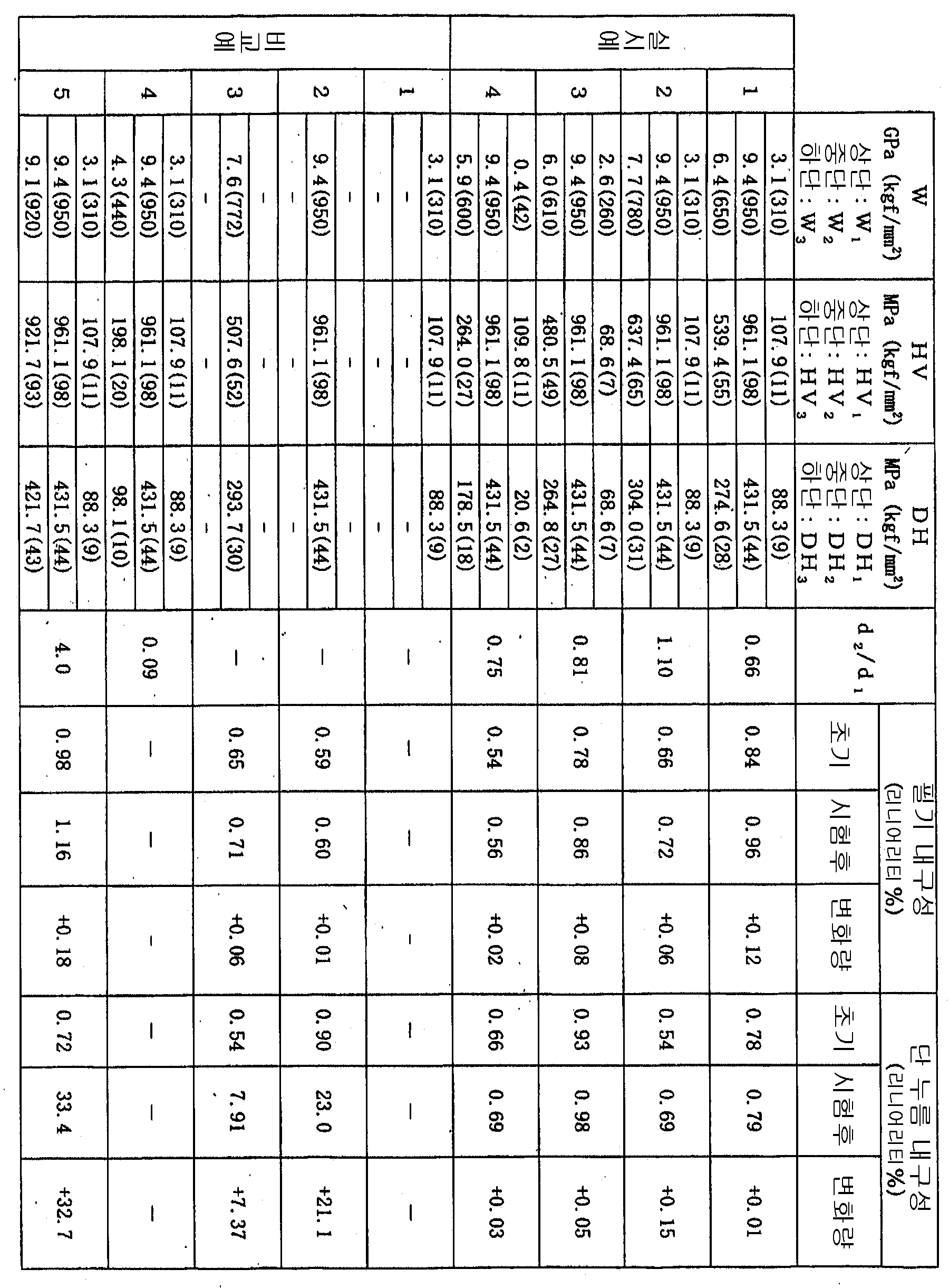
여기서, 비교예 1, 비교예 4 에서는 가동 전극 기판 열처리 후에 ITO 면에 미세한 주름이 발생하여 헤이즈가 상승 (백화) 하였기 때문에 필기 내구성 및 단 누름 내구성 시험을 실시하지 않았다. 또한, 표 중의 각 약호는 아래와 같다.Here, in Comparative Examples 1 and 4, since the fine wrinkles occurred on the ITO surface after the heat treatment of the movable electrode substrate, the haze increased (whitening), the writing durability and the short-press durability test were not performed. In addition, each symbol in a table | surface is as follows.
W1 : 경화 수지층-1 단독에서의 압입 시험에 의한 영률W 1 : Young's modulus by indentation test in cured resin layer-1 alone
W2 : 경화 수지층-2 단독에서의 압입 시험에 의한 영률W 2 : Young's modulus by indentation test in cured resin layer-2 alone
W3 : 경화 수지층-1 과 경화 수지층-2 를 적층한 후의 압입 시험에 의한 영률W 3 : Young's modulus by indentation test after laminating cured resin layer-1 and cured resin layer-2
HV1 : 경화 수지층-1 단독에서의 압입 시험에 의한 소성 변형 경도HV 1 : Plastic deformation hardness by indentation test in cured resin layer-1 alone
HV2 : 경화 수지층-2 단독에서의 압입 시험에 의한 소성 변형 경도HV 2 : Plastic deformation hardness by indentation test in cured resin layer-2 alone
HV3 : 경화 수지층-1 과 경화 수지층-2 를 적층한 후의 압입 시험에 의한 소성 변형 경도HV 3 : Plastic deformation hardness by indentation test after laminating cured resin layer-1 and cured resin layer-2
DH1 : 경화 수지층-1 단독에서의 압입 시험에 의한 경도DH 1 : Hardness by indentation test in cured resin layer-1 alone
DH2 : 경화 수지층-2 단독에서의 압입 시험에 의한 경도DH 2 : hardness by indentation test in the cured resin layer-2 alone
DH3: 경화 수지층-1 과 경화 수지층-2 를 적층한 후의 압입 시험에 의한 경도DH 3 : Hardness by indentation test after laminating cured resin layer-1 and cured resin layer-2
d1 : 경화 수지층-1 의 막두께d 1 : film thickness of cured resin layer-1
d2 : 경화 수지층-2 의 막두께d 2 : film thickness of cured resin layer-2
Claims (26)
Applications Claiming Priority (4)
| Application Number | Priority Date | Filing Date | Title |
|---|---|---|---|
| JPJP-P-2004-00259673 | 2004-09-07 | ||
| JP2004259673A JP2005104141A (en) | 2003-09-11 | 2004-09-07 | Transparent conductive laminate and transparent touch panel |
| JPJP-P-2004-00260750 | 2004-09-08 | ||
| JP2004260750A JP2005116515A (en) | 2003-09-17 | 2004-09-08 | Transparent conductive laminate and transparent touch panel |
Publications (1)
| Publication Number | Publication Date |
|---|---|
| KR20070051307A true KR20070051307A (en) | 2007-05-17 |
Family
ID=36036155
Family Applications (1)
| Application Number | Title | Priority Date | Filing Date |
|---|---|---|---|
| KR1020077005418A Withdrawn KR20070051307A (en) | 2004-09-07 | 2004-12-27 | Transparent conductive laminate and transparent touch panel |
Country Status (5)
| Country | Link |
|---|---|
| US (1) | US20070298231A1 (en) |
| EP (1) | EP1787795A1 (en) |
| KR (1) | KR20070051307A (en) |
| TW (1) | TW200609952A (en) |
| WO (1) | WO2006027859A1 (en) |
Cited By (3)
| Publication number | Priority date | Publication date | Assignee | Title |
|---|---|---|---|---|
| WO2011011701A3 (en) * | 2009-07-23 | 2011-06-16 | Saint-Gobain Performance Plastics Corporation | Composite cushioning structure |
| US8969222B2 (en) | 2008-12-22 | 2015-03-03 | Saint-Gobain Performance Plastics Corporation | Modified perfluoropolymer sheet material and methods for making same |
| US11230648B2 (en) | 2016-10-24 | 2022-01-25 | Saint-Gobain Performance Plastics Corporation | Polymer compositions, materials, and methods of making |
Families Citing this family (15)
| Publication number | Priority date | Publication date | Assignee | Title |
|---|---|---|---|---|
| US7333092B2 (en) | 2002-02-25 | 2008-02-19 | Apple Computer, Inc. | Touch pad for handheld device |
| JP4605788B2 (en) | 2006-04-27 | 2011-01-05 | 日東電工株式会社 | Touch panel |
| US8022935B2 (en) | 2006-07-06 | 2011-09-20 | Apple Inc. | Capacitance sensing electrode with integrated I/O mechanism |
| US8274479B2 (en) * | 2006-10-11 | 2012-09-25 | Apple Inc. | Gimballed scroll wheel |
| US11327621B2 (en) | 2007-01-16 | 2022-05-10 | Teijin Limited | Transparent conductive multilayer body and touch panel made of the same |
| JP5033740B2 (en) * | 2007-10-26 | 2012-09-26 | 帝人株式会社 | Transparent conductive laminate and touch panel |
| US9660218B2 (en) * | 2009-09-15 | 2017-05-23 | Industrial Technology Research Institute | Package of environmental sensitive element |
| CN102686057A (en) * | 2011-03-18 | 2012-09-19 | 深圳富泰宏精密工业有限公司 | Electronic device shell and manufacturing method thereof |
| KR101332442B1 (en) | 2011-09-21 | 2013-11-25 | 제일모직주식회사 | Composite sheet and substrate for display device comprising the same |
| JP6138598B2 (en) * | 2013-06-07 | 2017-05-31 | リンテック株式会社 | Hard coat film and method for producing the same |
| CN103700517B (en) * | 2013-12-31 | 2015-10-07 | 南通万德科技有限公司 | Switch contact element and preparation method thereof |
| JP6637286B2 (en) * | 2014-10-24 | 2020-01-29 | 積水化学工業株式会社 | Light transmitting conductive film and light transmitting film with hard coat |
| KR102563741B1 (en) * | 2016-09-06 | 2023-08-08 | 삼성디스플레이 주식회사 | Display device |
| KR102424954B1 (en) | 2017-08-07 | 2022-07-26 | 삼성디스플레이 주식회사 | Input sensing unit and display device having the same |
| EP3498452A3 (en) * | 2017-12-18 | 2019-08-28 | Ricoh Company, Ltd. | Method and apparatus for forming three-dimensional curved surface on laminated substrate, and three-dimensional curved laminated substrate |
Family Cites Families (8)
| Publication number | Priority date | Publication date | Assignee | Title |
|---|---|---|---|---|
| JPH10177101A (en) * | 1996-12-18 | 1998-06-30 | Sekisui Chem Co Ltd | Low-reflective laminate, optical element, display, and method for producing low-reflective laminate |
| JP3718031B2 (en) * | 1997-07-23 | 2005-11-16 | 富士写真フイルム株式会社 | Antireflection film and image display device using the same |
| JP4075147B2 (en) * | 1998-08-04 | 2008-04-16 | 凸版印刷株式会社 | Hard coat film or sheet, and hard coat film or sheet with functional inorganic thin film |
| US6489015B1 (en) * | 1998-11-17 | 2002-12-03 | Dai Nippon Printing Co., Ltd. | Hardcoat film and antireflection film |
| DE60045758D1 (en) * | 1999-08-31 | 2011-05-05 | Teijin Ltd | TRANSPARENT CONDUCTIVE MULTILAYER BODY AND THEREFORE PROVIDED TOUCH-SENSITIVE SCREEN |
| JP2002036436A (en) * | 2000-07-19 | 2002-02-05 | Fuji Photo Film Co Ltd | Hard coat film and hard coat film with functional thin film |
| US7294395B2 (en) * | 2001-09-03 | 2007-11-13 | Teijin Limited | Transparent electroconductive laminate |
| JP4052021B2 (en) * | 2002-06-04 | 2008-02-27 | 帝人デュポンフィルム株式会社 | Oriented polyester film and laminated film using the same |
-
2004
- 2004-12-27 KR KR1020077005418A patent/KR20070051307A/en not_active Withdrawn
- 2004-12-27 US US11/661,759 patent/US20070298231A1/en not_active Abandoned
- 2004-12-27 EP EP04808157A patent/EP1787795A1/en not_active Withdrawn
- 2004-12-27 WO PCT/JP2004/019807 patent/WO2006027859A1/en not_active Ceased
- 2004-12-28 TW TW093141010A patent/TW200609952A/en unknown
Cited By (3)
| Publication number | Priority date | Publication date | Assignee | Title |
|---|---|---|---|---|
| US8969222B2 (en) | 2008-12-22 | 2015-03-03 | Saint-Gobain Performance Plastics Corporation | Modified perfluoropolymer sheet material and methods for making same |
| WO2011011701A3 (en) * | 2009-07-23 | 2011-06-16 | Saint-Gobain Performance Plastics Corporation | Composite cushioning structure |
| US11230648B2 (en) | 2016-10-24 | 2022-01-25 | Saint-Gobain Performance Plastics Corporation | Polymer compositions, materials, and methods of making |
Also Published As
| Publication number | Publication date |
|---|---|
| EP1787795A1 (en) | 2007-05-23 |
| US20070298231A1 (en) | 2007-12-27 |
| WO2006027859A1 (en) | 2006-03-16 |
| TW200609952A (en) | 2006-03-16 |
Similar Documents
| Publication | Publication Date | Title |
|---|---|---|
| KR101143281B1 (en) | Transparent conductive multilayer body and transparent touch panel | |
| EP2211356B1 (en) | Transparent conductive laminate and transparent touch panel | |
| JP4869178B2 (en) | Transparent conductive laminate and transparent touch panel using the same | |
| EP2109116B1 (en) | Transparent conductive multilayer body and touch panel made of the same | |
| KR101067310B1 (en) | Transparent conductive laminate and transparent touch panel using the same | |
| KR20070051307A (en) | Transparent conductive laminate and transparent touch panel | |
| JP2007042284A (en) | Transparent conductive lamination body and transparent touch panel | |
| JP2005104141A (en) | Transparent conductive laminate and transparent touch panel | |
| JP2005116515A (en) | Transparent conductive laminate and transparent touch panel | |
| JP2006252875A (en) | Transparent conductive laminate and transparent touch panel | |
| JP2007042283A (en) | Transparent conductive lamination body and transparent touch panel | |
| JP2005014572A (en) | Transparent and conductive laminate showing excellent edge push durability | |
| JP2006190512A (en) | Transparent conductive laminate and transparent touch panel using it | |
| JP2006190508A (en) | Transparent conductive laminate and transparent touch panel using it | |
| WO2005036565A1 (en) | Transparent conductive laminate and transparent touch panel | |
| JP2006190510A (en) | Transparent conductive laminate and transparent touch panel using it | |
| JP2006190511A (en) | Transparent conductive laminate and transparent touch panel using it | |
| JP2006190509A (en) | Transparent conductive laminate and transparent touch panel using it | |
| HK1106320A (en) | Transparent conductive multilayer body and transparent touch panel | |
| HK1109493B (en) | Transparent conductive multilayer body and transparent touch panel | |
| HK1148861B (en) | Transparent conductive laminate and transparent touch panel |
Legal Events
| Date | Code | Title | Description |
|---|---|---|---|
| PA0105 | International application |
Patent event date: 20070307 Patent event code: PA01051R01D Comment text: International Patent Application |
|
| PG1501 | Laying open of application | ||
| PC1203 | Withdrawal of no request for examination | ||
| WITN | Application deemed withdrawn, e.g. because no request for examination was filed or no examination fee was paid |