KR20060108617A - Voltage converters, power management devices and mobile devices including them - Google Patents
Voltage converters, power management devices and mobile devices including them Download PDFInfo
- Publication number
- KR20060108617A KR20060108617A KR1020067007608A KR20067007608A KR20060108617A KR 20060108617 A KR20060108617 A KR 20060108617A KR 1020067007608 A KR1020067007608 A KR 1020067007608A KR 20067007608 A KR20067007608 A KR 20067007608A KR 20060108617 A KR20060108617 A KR 20060108617A
- Authority
- KR
- South Korea
- Prior art keywords
- voltage
- inverting
- inductive
- circuit
- branches
- Prior art date
- Legal status (The legal status is an assumption and is not a legal conclusion. Google has not performed a legal analysis and makes no representation as to the accuracy of the status listed.)
- Withdrawn
Links
- 230000001939 inductive effect Effects 0.000 claims abstract description 40
- 230000005415 magnetization Effects 0.000 claims abstract description 16
- 230000005347 demagnetization Effects 0.000 claims abstract description 10
- 238000000034 method Methods 0.000 claims description 9
- 230000003213 activating effect Effects 0.000 claims description 2
- 238000007599 discharging Methods 0.000 claims description 2
- HEZMWWAKWCSUCB-PHDIDXHHSA-N (3R,4R)-3,4-dihydroxycyclohexa-1,5-diene-1-carboxylic acid Chemical compound O[C@@H]1C=CC(C(O)=O)=C[C@H]1O HEZMWWAKWCSUCB-PHDIDXHHSA-N 0.000 description 14
- 239000003990 capacitor Substances 0.000 description 13
- 230000001276 controlling effect Effects 0.000 description 4
- 239000000872 buffer Substances 0.000 description 3
- 238000004146 energy storage Methods 0.000 description 3
- 230000000630 rising effect Effects 0.000 description 2
- 240000001973 Ficus microcarpa Species 0.000 description 1
- 230000001419 dependent effect Effects 0.000 description 1
- 230000000694 effects Effects 0.000 description 1
- 230000001976 improved effect Effects 0.000 description 1
- 230000001105 regulatory effect Effects 0.000 description 1
Images


Classifications
-
- H—ELECTRICITY
- H02—GENERATION; CONVERSION OR DISTRIBUTION OF ELECTRIC POWER
- H02M—APPARATUS FOR CONVERSION BETWEEN AC AND AC, BETWEEN AC AND DC, OR BETWEEN DC AND DC, AND FOR USE WITH MAINS OR SIMILAR POWER SUPPLY SYSTEMS; CONVERSION OF DC OR AC INPUT POWER INTO SURGE OUTPUT POWER; CONTROL OR REGULATION THEREOF
- H02M3/00—Conversion of DC power input into DC power output
- H02M3/02—Conversion of DC power input into DC power output without intermediate conversion into AC
- H02M3/04—Conversion of DC power input into DC power output without intermediate conversion into AC by static converters
- H02M3/06—Conversion of DC power input into DC power output without intermediate conversion into AC by static converters using resistors or capacitors, e.g. potential divider
- H02M3/07—Conversion of DC power input into DC power output without intermediate conversion into AC by static converters using resistors or capacitors, e.g. potential divider using capacitors charged and discharged alternately by semiconductor devices with control electrode, e.g. charge pumps
- H02M3/073—Charge pumps of the Schenkel-type
-
- H—ELECTRICITY
- H02—GENERATION; CONVERSION OR DISTRIBUTION OF ELECTRIC POWER
- H02M—APPARATUS FOR CONVERSION BETWEEN AC AND AC, BETWEEN AC AND DC, OR BETWEEN DC AND DC, AND FOR USE WITH MAINS OR SIMILAR POWER SUPPLY SYSTEMS; CONVERSION OF DC OR AC INPUT POWER INTO SURGE OUTPUT POWER; CONTROL OR REGULATION THEREOF
- H02M3/00—Conversion of DC power input into DC power output
- H02M3/02—Conversion of DC power input into DC power output without intermediate conversion into AC
- H02M3/04—Conversion of DC power input into DC power output without intermediate conversion into AC by static converters
- H02M3/10—Conversion of DC power input into DC power output without intermediate conversion into AC by static converters using discharge tubes with control electrode or semiconductor devices with control electrode
- H02M3/145—Conversion of DC power input into DC power output without intermediate conversion into AC by static converters using discharge tubes with control electrode or semiconductor devices with control electrode using devices of a triode or transistor type requiring continuous application of a control signal
- H02M3/155—Conversion of DC power input into DC power output without intermediate conversion into AC by static converters using discharge tubes with control electrode or semiconductor devices with control electrode using devices of a triode or transistor type requiring continuous application of a control signal using semiconductor devices only
- H02M3/156—Conversion of DC power input into DC power output without intermediate conversion into AC by static converters using discharge tubes with control electrode or semiconductor devices with control electrode using devices of a triode or transistor type requiring continuous application of a control signal using semiconductor devices only with automatic control of output voltage or current, e.g. switching regulators
- H02M3/158—Conversion of DC power input into DC power output without intermediate conversion into AC by static converters using discharge tubes with control electrode or semiconductor devices with control electrode using devices of a triode or transistor type requiring continuous application of a control signal using semiconductor devices only with automatic control of output voltage or current, e.g. switching regulators including plural semiconductor devices as final control devices for a single load
-
- H—ELECTRICITY
- H02—GENERATION; CONVERSION OR DISTRIBUTION OF ELECTRIC POWER
- H02M—APPARATUS FOR CONVERSION BETWEEN AC AND AC, BETWEEN AC AND DC, OR BETWEEN DC AND DC, AND FOR USE WITH MAINS OR SIMILAR POWER SUPPLY SYSTEMS; CONVERSION OF DC OR AC INPUT POWER INTO SURGE OUTPUT POWER; CONTROL OR REGULATION THEREOF
- H02M3/00—Conversion of DC power input into DC power output
- H02M3/02—Conversion of DC power input into DC power output without intermediate conversion into AC
- H02M3/04—Conversion of DC power input into DC power output without intermediate conversion into AC by static converters
- H02M3/06—Conversion of DC power input into DC power output without intermediate conversion into AC by static converters using resistors or capacitors, e.g. potential divider
- H02M3/07—Conversion of DC power input into DC power output without intermediate conversion into AC by static converters using resistors or capacitors, e.g. potential divider using capacitors charged and discharged alternately by semiconductor devices with control electrode, e.g. charge pumps
-
- H—ELECTRICITY
- H02—GENERATION; CONVERSION OR DISTRIBUTION OF ELECTRIC POWER
- H02M—APPARATUS FOR CONVERSION BETWEEN AC AND AC, BETWEEN AC AND DC, OR BETWEEN DC AND DC, AND FOR USE WITH MAINS OR SIMILAR POWER SUPPLY SYSTEMS; CONVERSION OF DC OR AC INPUT POWER INTO SURGE OUTPUT POWER; CONTROL OR REGULATION THEREOF
- H02M3/00—Conversion of DC power input into DC power output
- H02M3/02—Conversion of DC power input into DC power output without intermediate conversion into AC
- H02M3/04—Conversion of DC power input into DC power output without intermediate conversion into AC by static converters
- H02M3/10—Conversion of DC power input into DC power output without intermediate conversion into AC by static converters using discharge tubes with control electrode or semiconductor devices with control electrode
- H02M3/145—Conversion of DC power input into DC power output without intermediate conversion into AC by static converters using discharge tubes with control electrode or semiconductor devices with control electrode using devices of a triode or transistor type requiring continuous application of a control signal
- H02M3/155—Conversion of DC power input into DC power output without intermediate conversion into AC by static converters using discharge tubes with control electrode or semiconductor devices with control electrode using devices of a triode or transistor type requiring continuous application of a control signal using semiconductor devices only
- H02M3/156—Conversion of DC power input into DC power output without intermediate conversion into AC by static converters using discharge tubes with control electrode or semiconductor devices with control electrode using devices of a triode or transistor type requiring continuous application of a control signal using semiconductor devices only with automatic control of output voltage or current, e.g. switching regulators
- H02M3/158—Conversion of DC power input into DC power output without intermediate conversion into AC by static converters using discharge tubes with control electrode or semiconductor devices with control electrode using devices of a triode or transistor type requiring continuous application of a control signal using semiconductor devices only with automatic control of output voltage or current, e.g. switching regulators including plural semiconductor devices as final control devices for a single load
- H02M3/1584—Conversion of DC power input into DC power output without intermediate conversion into AC by static converters using discharge tubes with control electrode or semiconductor devices with control electrode using devices of a triode or transistor type requiring continuous application of a control signal using semiconductor devices only with automatic control of output voltage or current, e.g. switching regulators including plural semiconductor devices as final control devices for a single load with a plurality of power processing stages connected in parallel
-
- H—ELECTRICITY
- H02—GENERATION; CONVERSION OR DISTRIBUTION OF ELECTRIC POWER
- H02M—APPARATUS FOR CONVERSION BETWEEN AC AND AC, BETWEEN AC AND DC, OR BETWEEN DC AND DC, AND FOR USE WITH MAINS OR SIMILAR POWER SUPPLY SYSTEMS; CONVERSION OF DC OR AC INPUT POWER INTO SURGE OUTPUT POWER; CONTROL OR REGULATION THEREOF
- H02M3/00—Conversion of DC power input into DC power output
- H02M3/02—Conversion of DC power input into DC power output without intermediate conversion into AC
- H02M3/04—Conversion of DC power input into DC power output without intermediate conversion into AC by static converters
- H02M3/10—Conversion of DC power input into DC power output without intermediate conversion into AC by static converters using discharge tubes with control electrode or semiconductor devices with control electrode
- H02M3/145—Conversion of DC power input into DC power output without intermediate conversion into AC by static converters using discharge tubes with control electrode or semiconductor devices with control electrode using devices of a triode or transistor type requiring continuous application of a control signal
- H02M3/155—Conversion of DC power input into DC power output without intermediate conversion into AC by static converters using discharge tubes with control electrode or semiconductor devices with control electrode using devices of a triode or transistor type requiring continuous application of a control signal using semiconductor devices only
- H02M3/156—Conversion of DC power input into DC power output without intermediate conversion into AC by static converters using discharge tubes with control electrode or semiconductor devices with control electrode using devices of a triode or transistor type requiring continuous application of a control signal using semiconductor devices only with automatic control of output voltage or current, e.g. switching regulators
- H02M3/158—Conversion of DC power input into DC power output without intermediate conversion into AC by static converters using discharge tubes with control electrode or semiconductor devices with control electrode using devices of a triode or transistor type requiring continuous application of a control signal using semiconductor devices only with automatic control of output voltage or current, e.g. switching regulators including plural semiconductor devices as final control devices for a single load
- H02M3/1588—Conversion of DC power input into DC power output without intermediate conversion into AC by static converters using discharge tubes with control electrode or semiconductor devices with control electrode using devices of a triode or transistor type requiring continuous application of a control signal using semiconductor devices only with automatic control of output voltage or current, e.g. switching regulators including plural semiconductor devices as final control devices for a single load comprising at least one synchronous rectifier element
-
- Y—GENERAL TAGGING OF NEW TECHNOLOGICAL DEVELOPMENTS; GENERAL TAGGING OF CROSS-SECTIONAL TECHNOLOGIES SPANNING OVER SEVERAL SECTIONS OF THE IPC; TECHNICAL SUBJECTS COVERED BY FORMER USPC CROSS-REFERENCE ART COLLECTIONS [XRACs] AND DIGESTS
- Y02—TECHNOLOGIES OR APPLICATIONS FOR MITIGATION OR ADAPTATION AGAINST CLIMATE CHANGE
- Y02B—CLIMATE CHANGE MITIGATION TECHNOLOGIES RELATED TO BUILDINGS, e.g. HOUSING, HOUSE APPLIANCES OR RELATED END-USER APPLICATIONS
- Y02B70/00—Technologies for an efficient end-user side electric power management and consumption
- Y02B70/10—Technologies improving the efficiency by using switched-mode power supplies [SMPS], i.e. efficient power electronics conversion e.g. power factor correction or reduction of losses in power supplies or efficient standby modes
Landscapes
- Engineering & Computer Science (AREA)
- Power Engineering (AREA)
- Dc-Dc Converters (AREA)
- Control Of Electrical Variables (AREA)
Abstract
전압 컨버터는 유도성 자화 모드 동안 에너지를 저장하며 유도성 자화 해제 모드 동안 에너지를 전달하는 유도성 회로(L)를 포함한다. 또한 전압 컨버터는 적어도 두개의 비반전 출력 전압(Va, Vb, Vc)을 제공하기 위한 적어도 두 개의 비반전 브랜치(12, 13, 14)와, 반전된 출력 전압을 제공하기 위한 반전 브랜치(15)를 포함한다. 상기 반전(15) 및 비반전(12, 13, 14) 브랜치는 상기 유도성 회로(L)의 출력단(10)에 나란하게 접속된다. 상기 유도성 회로는 상기 반전 브랜치(15) 및 상기 적어도 두개의 비 반전 브랜치(12, 13, 14) 중의 하나에 에너지를 전달하도록 배열된다. 이를 통해, 상기 반전 전압(Vinv)과 상기 적어도 두개의 비반전 브랜치(12, 13, 14) 중의 하나의 대응 비반전 출력 전압(Va, Vb, Vc)은 대향 극성을 가지며 실질적으로 동일한 크기를 갖는다.The voltage converter includes an inductive circuit L that stores energy during the inductive magnetization mode and delivers energy during the inductive demagnetization mode. The voltage converter also has at least two non-inverting branches 12, 13, 14 for providing at least two non-inverting output voltages Va, Vb, Vc, and an inverting branch 15 for providing an inverted output voltage. It includes. The inverting 15 and non-inverting branches 12, 13 and 14 are connected side by side to the output terminal 10 of the inductive circuit L. The inductive circuit is arranged to transfer energy to one of the inverted branch 15 and the at least two non-inverted branches 12, 13, 14. In this way, the inversion voltage Vinv and the corresponding non-inverting output voltages Va, Vb, Vc of the at least two non-inverting branches 12, 13, 14 have opposite polarities and have substantially the same magnitude. .
Description
본 발명은 전압 컨버터, 전력 관리 장치 및 전압 컨버터를 포함한 모바일 장치에 관한 것이다.The present invention relates to a mobile device including a voltage converter, a power management device and a voltage converter.
본 발명은 가령, 전력 공급원 혹은 모바일 장치(가령, 모바일 폰, PDA 또는 랩톱)에서 사용될 수 있다. 전압 컨버터는 일반적으로 DC 입력 전압원으로부터 다수의 DC 출력 전압을 유도하기 위해 사용된다. 이러한 출력 전압은 DC 입력 전압보다 높은 전압 레벨을 가질 수 있다. 전압 컨버터는 통상적으로 DCDC 전압 컨버터 혹은 스위치형 모드 전력 공급원(SMPS)으로 지칭되기도 한다. DCDC 컨버터는 일반적으로 당해 기술분야에서 잘 알려져 있다. 전압 컨버터는 DC 입력 전압원으로부터 획득되는 에너지를 저장하는 인터터와 같은 에너지 저장 수단을 포함한다. 이러한 에너지는 나중에 다수의 출력 전압을 생성하고 유지하기 위해 사용된다. 에너지 저장 수단은 주기적으로 충전 및 방전되고 에너지 저장 수단으로부터 전압 컨버터의 출력단으로의 에너지 흐름은 프로그램가능한 스위치 장치에 의해 조절된 다. 또한 전압 컨버터의 출력단 중의 임의의 출력단에 접속된 인버팅 회로를 사용함으로써 네가티브 전압이 제공될 수도 있다는 것은 당해 기술분야에서 일반적으로 알려진 것이다.The invention can be used, for example, in a power supply or in a mobile device (eg, mobile phone, PDA or laptop). Voltage converters are commonly used to derive multiple DC output voltages from a DC input voltage source. This output voltage can have a higher voltage level than the DC input voltage. The voltage converter is also commonly referred to as a DCDC voltage converter or switched mode power supply (SMPS). DCDC converters are generally well known in the art. The voltage converter comprises energy storage means, such as an intert, which stores energy obtained from a DC input voltage source. This energy is later used to generate and maintain multiple output voltages. The energy storage means are charged and discharged periodically and the energy flow from the energy storage means to the output of the voltage converter is regulated by a programmable switch device. It is also generally known in the art that a negative voltage may be provided by using an inverting circuit connected to any of the output stages of the voltage converter.
본 발명의 목적은 개선된 전압 컨버터를 제공하는 것이다. 이러한 목적 달성을 위해 전압 컨버터는 유도성 자화 모드 동안 에너지를 저장하며 유도성 자화 해제 모드 동안 에너지를 전달하는 유도성 회로와, 적어도 두개의 비반전 출력 전압을 제공하기 위한 적어도 두개의 비반전 브랜치와, 반전된 출력 전압을 제공하기 위한 반전 브랜치를 포함하되, 상기 반전 및 비반전 브랜치는 상기 유도성 회로의 출력단에 평행하게 접속되며, 상기 유도성 회로는 에너지를 상기 반전 브랜치 및 적어도 두개의 비반전 브랜치 중의 하나로 전달하도록 배열되며, 상기 반전 전압 및 상기 적어도 두개의 비반전 브랜치 중의 하나의 해당 비반전 출력 전압이 대향되는 극성과 실질적으로 동일한 크기를 갖는다.It is an object of the present invention to provide an improved voltage converter. To achieve this goal, a voltage converter includes an inductive circuit that stores energy during inductive magnetization mode and delivers energy during inductive demagnetization mode, and at least two non-inverting branches to provide at least two non-inverting output voltages. And an inverting branch for providing an inverted output voltage, wherein the inverting and non-inverting branches are connected in parallel to the output of the inductive circuit, the inductive circuit transferring energy to the inverting branch and at least two non-inverting branches. Arranged to deliver to one of the branches, the inversion voltage and the corresponding non-inverting output voltage of one of the at least two non-inverting branches have a magnitude substantially equal to the opposite polarity.
본 발명은 상기 반전 브랜치를 비반전 브랜치의 출력단보다는 유도성 회로의 출력단에 접속함으로써 보다 더 효율적이고 보다 더 비용 절감적인 전압 컨버터의 디자인을 가능하게 하는 요구된 스위치 장치에서 상당한 절감을 달성할 수 있다는 통찰력에 토대를 두고 있다. 본 발명은 또한 상기 비반전 및 반전 브랜치의 출력 전압이 상기 유도성 회로의 출력단에서 이용가능한 전압 클램프 레벨에 의해 결정되어 상기 반전 브랜치와 상기 비반전 브랜치의 출력단을 더 이상 접속할 필요가 없다는 통찰력에 토대를 두고 있다.The present invention can achieve significant savings in the required switch arrangement which enables the design of a more efficient and more cost-effective voltage converter by connecting the inverted branch to the output of the inductive circuit rather than to the output of the non-inverted branch. It is based on insight. The present invention is also based on the insight that the output voltages of the non-inverting and inverting branches are determined by the voltage clamp level available at the output of the inductive circuit so that it is no longer necessary to connect the inverting branch and the output of the non-inverting branch. I put it.
본 발명에 따른 전압 컨버터의 다른 실시예에서, 상기 반전 브랜치는 상기 유도성 자화 해제 모드 동안 상기 전달된 에너지를 저장하고 상기 유도성 자화 모드 동안 상기 전달된 에너지를 배출하기 위한 용량성 회로를 포함한다. 캐패시터는 바람직하게도 먼저 요구된 전압 레벨에 도달될 때까지 충전되며 이후에 요구시 충전 해제되는 배터리로서 기능할 수가 있다.In another embodiment of the voltage converter according to the invention, the inverting branch comprises a capacitive circuit for storing the delivered energy during the inductive magnetization mode and discharging the delivered energy during the inductive magnetization mode. . The capacitor may preferably function as a battery which is first charged until the required voltage level is reached and subsequently decharged on demand.
본 발명에 따른 전압 컨버터의 실시예에서, 용량성 회로는 용량성 회로의 출력단이 접지 전압에 접속되는 동안 상기 전달된 에너지를 용량성 회로의 입력단을 통해 수신하도록 배열되고, 그 입력단이 접지 전압에 접속되는 동안 그 출력단을 통해 에너지를 배출하도록 배열된다. 이러한 실시예는 캐패시터 양단의 전압의 극성을 반전시키는 편리한 방식을 제공한다는 효과를 갖는다.In an embodiment of the voltage converter according to the invention, the capacitive circuit is arranged to receive the transferred energy through the input of the capacitive circuit while the output of the capacitive circuit is connected to the ground voltage, the input of which is connected to the ground voltage. It is arranged to discharge energy through its output stage while connected. This embodiment has the effect of providing a convenient way to reverse the polarity of the voltage across the capacitor.
본 발명에 따른 전압 컨버터의 다른 실시예에서, 전압 컨버터는 제각기의 유도성 자화 모드 및 자화 해제 모드 동안 용량성 회로의 입력단(In) 및 출력단(Out)을 제각기 접지 전압(GND)에 접속하는 제 1 및 제 2 스위치 장치를 포함한다. 상기 제 1 및 제 2 스위치 장치에 의해, 상기 용량성 회로는 제어 방식으로 용이하게 충전 및 충전 해제될 수 있다.In another embodiment of the voltage converter according to the invention, the voltage converter is configured to connect the input terminal (In) and the output terminal (Out) of the capacitive circuit to the ground voltage (GND) respectively during the inductive magnetization mode and the demagnetization mode, respectively. A first and a second switch device. By the first and second switch devices, the capacitive circuit can be easily charged and decharged in a controlled manner.
본 발명에 따른 전압 컨버터의 실시예에서, 전압 컨버터는 전압 다운 컨버터 회로를 포함하며, 이 전압 다운 컨버터 회로를 통해 입력 전압이 유도성 회로에 인가된다. 이와 함께, 유도성 회로 내에서 생성된 충전 양과 전압 컨버터의 출력 전압이 제어될 수 있다.In an embodiment of the voltage converter according to the invention, the voltage converter comprises a voltage down converter circuit through which an input voltage is applied to the inductive circuit. In addition, the amount of charge generated in the inductive circuit and the output voltage of the voltage converter can be controlled.
본 발명에 따른 전압 컨버터의 실시예에서, 전압 다운 컨버터 회로는 상기 유도성 회로에 입력 전압과 접지 전압을 교번적으로 인가하기 위한 제 3 스위치 장치 및 제 4 스위치 장치를 포함한다. 이 실시예는 전압 다운 컨버팅된 양이 제 3 스위치 장치 및 제 4 스위치 장치의 듀티 사이클에 의해 결정될 수 있다는 이점을 갖는다. 이를 통해, 프로그램가능한 전압 다운 컨버터 회로를 획득할 수 있다.In an embodiment of the voltage converter according to the invention, the voltage down converter circuit comprises a third switch device and a fourth switch device for alternately applying an input voltage and a ground voltage to the inductive circuit. This embodiment has the advantage that the amount of voltage down converted can be determined by the duty cycle of the third switch device and the fourth switch device. This makes it possible to obtain a programmable voltage down converter circuit.
본 발명에 따른 전압 컨버터의 실시예에서, 상기 적어도 두개의 브랜치 중의 적어도 하나는 상기 브랜치를 활성화하기 위한 추가의 스위치 장치를 포함한다. 이 추가의 스위치 장치에 의해, 상기 유도성 회로로부터의 에너지 흐름이 제어될 수 있다. 이는 단지 추가의 스위치 장치만이 클로져된다면 에너지가 상기 브랜치로 전달될 것이라는 것을 의미한다. 또한, 이 추가의 스위치 장치가 클로져된다면, 반전 브랜치의 클램프 전압의 크기는 활성화된 비반전 브랜치의 클램프 전압의 크기와 실질적으로 동일하게 될 것이다.In an embodiment of the voltage converter according to the invention, at least one of the at least two branches comprises an additional switch device for activating the branch. By this further switch device, the energy flow from the inductive circuit can be controlled. This means that if only an additional switch device is closed, energy will be transferred to the branch. Also, if this additional switch device is closed, the magnitude of the clamp voltage of the inverted branch will be substantially equal to the magnitude of the clamp voltage of the activated non-inverted branch.
본 발명에 따른 전압 컨버터의 다른 실시예에서, 전압 컨버터는 상기 스위치 장치들을 제어하기 위한 제어 수단을 더 포함한다. 스위치를 제어함으로써 전압 컨버터의 동작 및 응답을 제어할 수가 있다.In another embodiment of the voltage converter according to the invention, the voltage converter further comprises control means for controlling the switch devices. By controlling the switch, the operation and response of the voltage converter can be controlled.
본 발명의 전술한 측면 및 기타 측면들은 후술되는 도면을 통해 설명될 것이다.The above and other aspects of the present invention will be described through the following drawings.
도 1은 종래 기술에 따른 전압 컨버터를 도시한 도면이다.1 is a view showing a voltage converter according to the prior art.
도 2는 종래 기술의 전압 컨버터 내의 인덕터 L을 통한 자화 전류 IL을 도시한 도면이다.2 shows the magnetizing current I L through the inductor L in a voltage converter of the prior art.
도 3은 종래 기술의 전압 컨버터 내의 인덕터 L의 양단의 전압 강하 UL을 도시한 도면이다.FIG. 3 shows the voltage drop U L across the inductor L in the voltage converter of the prior art.
도 4는 용량성 DCDC 인버터를 도시한 도면이다.4 shows a capacitive DCDC inverter.
도 5는 종래 기술에 따른 용량성 DCDC 인버터를 포함한 전압 컨버터를 도시한 도면이다.5 illustrates a voltage converter including a capacitive DCDC inverter according to the prior art.
도 6은 본 발명에 따른 용량성 DCDC 인버터를 포함한 전압 컨버터를 도시한 도면이다.6 illustrates a voltage converter including a capacitive DCDC inverter according to the present invention.
도 7은 본 발명에 따른 용량성 DCDC 인버터를 포함한 전압 컨버터의 스위칭 시퀀스를 도시한 도면이다.7 illustrates a switching sequence of a voltage converter including a capacitive DCDC inverter according to the present invention.
도 8은 입력 전압 감소 수단을 포함한 종래 기술에 따른 다른 전압 컨버터를 도시한 도면이다.8 shows another voltage converter according to the prior art including an input voltage reducing means.
도 1은 입력 전압 Vi를 세개의 클램프 전압 Va, Vb, Vc로 변환시키는 종래의 전압 컨버터를 도시한 도면이다. 도 1에서, Va 〉Vb 〉Vc로 간주된다. 저항기 RL1, RL2, RL3은 전압 컨버터의 부하를 나타낸다. 클램프 전압 Va, Vb, Vc는 본 기술 분야에서 일반적으로 알려진 방법에 따라 생성된다. 가령, 클램프 전압 Va, Vb, Vc를 측정하거나 혹은 회로 부하 RL1, RL2, RL3를 통한 전류를 측정하는 것에 응답하여 유도성 자화 모드 및 자화 해제 모드의 듀티 사이클을 제어함으로써 생성된다.1 illustrates a conventional voltage converter for converting an input voltage Vi into three clamp voltages V a , V b , V c . In FIG. 1, V a > V b > V c . Resistors R L1 , R L2 , R L3 represent the load of the voltage converter. Clamp voltage V a, V b, V c is produced in accordance with methods generally known in the art. For example, by controlling the duty cycles of inductive magnetization mode and demagnetization mode in response to measuring clamp voltages V a , V b , V c or measuring current through circuit loads R L1 , R L2 , R L3 . do.
유도성 자화 모드 동안, 스위치 SL은 클로즈(도전 상태)되고, 반면 D1, S5 및 S6은 비도전 상태로 된다. 분명하게도, 자화 전류 IL은 I1과 동일하다. 당업자라면 I1이 I1=(Vi/L)*t와 동일하다는 것을 쉽게 증명할 수 있으며, 여기서 L은 인덕터 L의 인덕턴스를 나타내며, t는 시간을 나타낸다. 따라서, 자화 전류 IL은 도 2의 곡선(20)으로 도시된 바와 같이 시간에 따라 Imax와 동일한 IL까지 지속적으로 증가할 것이다. 유도성 자화 모드 동안 전류 IL은 E=1/2 *L * Imax2와 동일한 에너지 E의 양을 유도성 회로 L로 전달한다는 것을 쉽게 증명할 수 있다.During inductive magnetization mode, the switch S L is closed (conductive state), while D1, S5 and S6 are in a non-conductive state. Clearly, the magnetizing current I L is equal to I 1 . One skilled in the art can easily prove that I 1 is equal to I 1 = (V i / L) * t, where L represents the inductance of the inductor L and t represents time. Thus, the magnetization current I L will continue to increase up to I L equal to I max over time, as shown by
유도성 자화 해제 모드 동안, 스위치 SL은 오픈되는 반면 동시에 스위칭 요소 D1, S5, S6 중의 하나는 도전 상태로 된다. 이러한 방식으로 저장된 에너지 E=1/2 *L * Imax2는 출력 브랜치(12, 13 또는 14) 위에 분포된다. 예를 통해, 도 1은 단지 S5만이 도전 상태로 되어 IL=I2가 된다고 가정된다. 본 기술분야에서 일반적으로 알려진 것은 인덕터 L이 급격한 전류 변화에 대해 저항성이 있다는 것이다. 따라서 I2는 Imax에서 출발하여 도 2의 곡선(22)에 도시된 바와 같이 선형 적으로 감소할 것이라는 것을 쉽게 증명할 수 있다. 도 2의 램프(22)의 각도α는 L*dIL/dt=(Vi-Vb+VD2)에 의해 결정되며, 이는 램프(22)의 각도가 주로 출력 전압 Vb에 의해 결정된다.During the inductive demagnetization mode, the switch S L is opened while at the same time one of the switching elements D1, S5, S6 is brought into a conductive state. The energy E = 1/2 * L * Imax 2 stored in this way is distributed over the
Vb는 Vb=Vi-L*dIL/dt+VD2로서 표현될 수 있다. 유도성 자화 해제 모드 동안, L*dIL/dt 볼트의 인덕터 L 양단의 전압은 네가티브 극성을 가질 것이며, 이는 가령 도 3의 곡선(32)에 도시된다. 그러나, -L*dIL/dt는 출력 전압 Vb에 대해 포지티브 분포를 가지는 것이 명백하다. VD2는 다이오드 D2 양단의 전압 강하를 나타내는데, 이 다이오드는 전형적으로 사용되는 기술에 따라 0.3과 0.7볼트 사이에 존재한다. 다이오드 D1, D2, D3는 전압 컨버터의 출력단으로부터 내부 노드(10)로 향하는 전류 누설을 방지하도록 제공된다. 다이오드 D1, D2, D3은 스위치 S5, S6이 염격하게도 단방향성, 즉 내부 노드(10)에서 출력으로만 도전하는 경우에 생략될 수 있다. 이러한 것은 가령, 스위치 S5, S6이 반 직렬로 접속되는 PMOS 트랜지스터의 쌍에 의해 구성될 경우이다. 이러한 경우 브랜치(12)는 스위치 장치를 포함해야만 한다. 만약 스위치 S5 및 S6이 개방된다면, 전류 I2는 브랜치(12)를 통해 흐르기 시작할 것이다. 만약 스위치 S5가 클로즈되고 S6이 개방된 채로 유지되면, Vb-VD2의 전압은 내부 노드(10) 상에 놓여질 것이다. 이러한 것이 Va보다 낮은 전압이기 때문에, 다이오드 D1는 턴오프될 것이고, I2는 제 2 브랜치(13)를 통해 흐르 기 시작할 것이다. 마찬가지로, 스위치 S6를 클로즈하면 내부 노드(10) 상에 Vc-VD3의 전압이 놓여지며, 이는 다이오드 D1 및 D2를 턴오프시킬 것이다. 스위치 SL, S5 및 S6을 제어 방식으로 동작시킴으로써 인덕터 L을 자화 및 자화 해제시킬 수 있으며 그리고 인덕터 L로부터 브랜치(12, 13, 14) 중의 각각으로 에너지를 전달할 수가 있다. 캐패시터 C1은 DC 입력 버퍼로서 기능하며, 이 버퍼는 전압 컨버터의 고주파 스위칭 입력 전류 및 스위칭 노이즈로부터 입력 라인을 보호한다. 캐패시터 C2, C3, C4는 DC 출력 버퍼로서 기능한다. 이러한 기능은 먼저 고주파 출력 전류를 평탄화하며 그리고 전압 컨버터의 브랜치에 전하가 제공되지 않을 때의 시간 주기 동안 연속적인 출력 전압을 보장하는 것이다. 이러한 결과로서, 캐패시터 C2, C3, C4 양단의 전압은 약간의 AC 리플을 보일 것이다. 그러나, 이는 거의 중요하지 않는데, 그 이유는 캐패시터 C2, C3, C4가 유도성 회로에 의해 매우 고속으로 재충전되기 때문이다.V b may be expressed as V b = V i -L * d L L / dt + V D2 . During inductive demagnetization mode, the voltage across inductor L of L * dI L / dt volts will have a negative polarity, which is shown, for example, in
도 2는 인덕터 L에 흐르는 자화 전류 IL을 도시한다. 상승 에지(20)는 인덕터의 충전 혹은 자화를 나타낸다(SL는 클로즈됨). 유도성 극대화 모드 동안 자화 전류 IL는 SL가 개방될 때까지 증가한다. IL가 Vi*t/L과 동일하며, t는 시간을 나타내며 L은 인덕터 L의 인덕턴스라는 것을 쉽게 증명할 수가 있다. 일단 SL가 개방되면, 전류 IL가 Imax와 동일하며 도 2에 도시된 바와 같이 하강 에지(22)를 나 타낼 것이다. 이 하강 에지는 dIL/dt=(Vi-Vout+VD)/L로서 표현될 수 있으며, Vi는 입력 전압을 나타낸다. Vout는 도 1의 출력 전압 Va, Vb, Vc 중의 임의의 것을 나타내며, VD는 다이오드들이 도전 상태에 있을 때 다이오드 D1, D2, D3 양단의 전압 강하를 나타낸다.2 shows the magnetizing current I L flowing through the inductor L. FIG. The rising
도 3은 UL=L*dIL/dt로서 표현될 수 있는 인덕터 L 양단의 전압 강하 UL을 도시한다. 이는 IL의 상승 에지(20) 동안 전압 UL의 포지티브 극성(30)을 생성하며, IL의 하승 에지(22) 동안 전압 UL의 네가티브 극성(32)을 생성한다.3 shows the voltage drop U L across the inductor L which can be expressed as U L = L * dI L / dt. This produces a
도 4는 DCDC 용량성 전압 컨버터를 도시한다. 도시된 것은 입력 전압 소스 Vi를 통해 충전되는 캐패시터 Cpump이다. 충전 동안, 스위치 S4, S2는 클로즈되는 반면 스위치 SL, S7은 개방된다. 이를 통해, Cpump는 Cpump 양단의 전압 강하가 Vi가 되고 도 4에 도시된 바와 같은 극성을 가질 때까지 충전될 것이다. 일단 Cpump가 완전히 충전된다면, 스위치 S4, S2는 궁극적으로 개방되고 스위치 SL, S7은 클로즈된다. 이 때문에, Cpump는 출력 용량성 전압 인버터에 접속되어 Vi와 동일한 크기를 갖지만 대향되는 극성을 갖는 출력 전압 Vinv를 전달한다. 캐패시터 Co는 DC 출력 버퍼로서, 컨버터의 고주파 출력 전력을 평탄화하며 펌프 캐패시터 Cpump가 재충전될 때 출력 전압 Vinv를 용량성 DCDC 인버터의 부하에 제공한다.4 shows a DCDC capacitive voltage converter. Shown is a capacitor Cpump being charged by the input voltage source V i. During charging, switches S4 and S2 are closed while switches S L and S7 are open. Through this, the Cpump will be charged until the voltage drop across the Cpump becomes V i and has the polarity as shown in FIG. 4. Once Cpump is fully charged, switches S4 and S2 ultimately open and switches S L and S7 are closed. Therefore, Cpump is connected to the output capacitive voltage inverter and delivers an output voltage Vinv having a polarity opposite to have the same size as V i. Capacitor Co is a DC output buffer that flattens the high frequency output power of the converter and provides the output voltage Vinv to the load of the capacitive DCDC inverter when the pump capacitor Cpump is recharged.
도 5는 도 1에 도시된 종래 기술의 DCDC 전압 컨버터와 도 4에 논의된 용량 성 DCDC 전압 인버터의 조합체를 도시한 도면이다. 캐패시터 Cpump는 교번 방식으로 동작하는 스위치 S4, S'4, S"4에 의해 브랜치(12, 13, 14)의 출력단에 접속된다. 가령, 스위치 S4, S2를 클로징함으로써, 펌프 캐패시터 Cpump는 전압 Vc로 충전된다. 스위치 S7, S1을 클로징하고 스위치 S4, S'4, S"4, S2를 개방함으로써 출력 전압 Vinv는 -Vc와 동일하게 된다.FIG. 5 shows a combination of the prior art DCDC voltage converter shown in FIG. 1 and the capacitive DCDC voltage inverter discussed in FIG. 4. The capacitor Cpump is connected to the output terminals of the
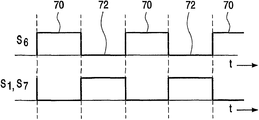
도 6은 본 발명에 따른 DCDC 전압 컨버터를 도시한 도면이다. 도시된 것은 내부 노드(10)에 접속된 용량성 DCDC 인버터이다. 이를 통해 Cpump는 유도성 자화 해제 모드 동안 노드(10)에서 이용가능한 전압으로 충전된다. 전술한 바와 같이, 이 전압은 입력 전압 Vi와 인덕터 L 양단의 전압 강하에 의해 결정된다. 분명하게도, 인덕터 양단의 전압 강하는 자화 해제 모드 동안 그로부터 유도되는 전류 I2 및 I'2에 의해 결정된다. 이를 통해 출력 전압 Vinv는 활성화되는 비반전 브랜치(12, 13, 14) 중의 임의의 것에 따라 클램프 전압 Va, Vb, Vc 중의 임의의 하나와 실질적으로 동일한 크기를 가질 수 있다. 제어 수단(82)을 제공함으로써, 스위치 S1, S2, S5, S6, S7의 듀티 사이클은 전압 컨버터의 동작에 영향을 미치도록 제어될 수 있다. 이러한 실시예는 여분의 제한된 양의 스위치가 요구되는 이점을 제공한다. 즉 스위치 S6, S7은 스위치의 제어를 위해 낮은 비용 및 적은 요건으로 집적하기에 더 용이한 회로를 만들게 하는 이점을 제공한다.6 illustrates a DCDC voltage converter according to the present invention. Shown is a capacitive DCDC inverter connected to the
도 7은 예를 통해 도 6의 스위치 S1, S6, S7을 제어하기 위한 스위칭 사이클을 나타낸다. 에너지는 비반전 브랜치(14)(요구시에 전달)에 제공되는 것으로 가 정된다. 이는 스위치 S5 및 S2가 클로즈되고 S6 및 S7이 개방된 채로 유지되는 것을 의미한다. 당업자에게 분명한 것은 노드(10)의 전압 레벨이 실질적으로 클램프 전압 Vb에 대응한다는 것이다. 이는 Cpump 양단의 전압이 또한 Vb가 될 것이라는 것을 의미한다. 다음 유도성 자화 모드(72) 동안, 스위치 S1 및 S7는 클로즈되어 전류 I1는 반전 브랜치 Vinv의 출력 전압이 -Vb가 되는 동안 인덕터 L을 에너지로 충전하기 위해 흐르기 시작할 것이다. 일단 Cpump가 반전 브랜치의 출력단에 접속되면, 캐패시터 Cpump 양단의 전압이 다소 감소할 것이라는 것이 명백하다. 따라서, 다음의 유도성 자화 해제 모드 동안, 스위치 S1 및 S7은 다시 개방되고 S6은 클로즈된다. 이는 Cpump가 에너지로 다시 채워지도록 하여, Vb의 전압 강하가 다시 캐패시터 Cpump 양단에 나타날 것이다.7 shows a switching cycle for controlling the switches S1, S6, S7 of FIG. 6 by way of example. It is assumed that energy is provided to the non-inverting branch 14 (delivered on demand). This means that switches S5 and S2 are closed and S6 and S7 remain open. It will be apparent to those skilled in the art that the voltage level of the
도 8은 DCDC 전압 컨버터를 도시한 것으로, 스위치 S3 및 S4에 의해, 접지 전압 GND 및 입력 전압 Vi가 교번적으로 인덕터 L에 접속되어 입력 전압 Vi의 평균값을 감소시킨다. 이러한 입력값의 감소는 DCDC 전압 컨버터의 출력 전압에 영향을 미치는데 효과적으로 사용된다는 것이 당업자에게는 명백하다.8 shows a DCDC voltage converter, by means of switches S3 and S4, the ground voltage GND and the input voltage V i are alternately connected to the inductor L to reduce the average value of the input voltage V i . It is apparent to those skilled in the art that this reduction in input value is effectively used to influence the output voltage of the DCDC voltage converter.
주목할 것은 전술한 실시예가 본 발명을 제한하기보다는 예시하는 것이며, 당업자라면 첨부된 청구범위의 영역 내에서 여러 다른 실시예를 디자인할 수 있을 것이라는 것이다. 단어 "포함"이라는 것은 청구범위에 열거된 요소 혹은 단계의 존재를 배제하는 것이 아니다. 단수의 요소는 그러한 요소의 복수 개의 존재를 배제하는 것이 아니다. 소정의 수단들이 상호 상이한 종속 청구항에서 인용된다 는 것은 그러한 수단들의 조합체가 사용될 수 없다는 것을 나타내는 것이 아니다.It is to be noted that the above-described embodiments illustrate rather than limit the invention, and those skilled in the art will be able to design many other embodiments within the scope of the appended claims. The word "comprising" does not exclude the presence of elements or steps listed in the claims. A singular element does not exclude a plurality of such elements. Reference to certain means by mutually different dependent claims does not indicate that a combination of such means cannot be used.
Claims (10)
Applications Claiming Priority (2)
| Application Number | Priority Date | Filing Date | Title |
|---|---|---|---|
| EP03103887.0 | 2003-10-21 | ||
| EP03103887 | 2003-10-21 |
Publications (1)
| Publication Number | Publication Date |
|---|---|
| KR20060108617A true KR20060108617A (en) | 2006-10-18 |
Family
ID=34443047
Family Applications (1)
| Application Number | Title | Priority Date | Filing Date |
|---|---|---|---|
| KR1020067007608A Withdrawn KR20060108617A (en) | 2003-10-21 | 2004-10-19 | Voltage converters, power management devices and mobile devices including them |
Country Status (7)
| Country | Link |
|---|---|
| US (1) | US7466114B2 (en) |
| EP (1) | EP1678817A1 (en) |
| JP (1) | JP2007509598A (en) |
| KR (1) | KR20060108617A (en) |
| CN (1) | CN1871760A (en) |
| TW (1) | TW200520355A (en) |
| WO (1) | WO2005039033A1 (en) |
Families Citing this family (18)
| Publication number | Priority date | Publication date | Assignee | Title |
|---|---|---|---|---|
| FR2909495B1 (en) * | 2006-12-05 | 2009-01-16 | Thales Sa | DC DC VOLTAGE ELEVATOR CONVERTER |
| JP2008148514A (en) * | 2006-12-13 | 2008-06-26 | Toppoly Optoelectronics Corp | Dcdc converter |
| US8614569B2 (en) * | 2007-04-24 | 2013-12-24 | St-Ericsson Sa | Method of controlling a switched-mode power supply having a single inductive element and several outputs, and corresponding power supply, in particular for a cellular mobile telephone |
| US7768756B2 (en) | 2007-04-27 | 2010-08-03 | Hewlett-Packard Development Company, L.P. | Leakage current protection circuit |
| US20090040794A1 (en) * | 2007-08-08 | 2009-02-12 | Advanced Analogic Technologies, Inc. | Time-Multiplexed Multi-Output DC/DC Converters and Voltage Regulators |
| TWI411210B (en) * | 2010-11-23 | 2013-10-01 | Univ Nat Chiao Tung | Freewheel charge-pump controlled single-inductor multiple-output dc-dc converter |
| EP2466738B1 (en) | 2010-12-20 | 2018-04-04 | ams AG | Voltage converter and method for voltage conversion |
| US8345030B2 (en) | 2011-03-18 | 2013-01-01 | Qualcomm Mems Technologies, Inc. | System and method for providing positive and negative voltages from a single inductor |
| TWI514738B (en) * | 2011-07-07 | 2015-12-21 | Sitronix Technology Corp | Voltage converter |
| US8786592B2 (en) * | 2011-10-13 | 2014-07-22 | Qualcomm Mems Technologies, Inc. | Methods and systems for energy recovery in a display |
| DE102011089648A1 (en) * | 2011-12-22 | 2013-06-27 | Robert Bosch Gmbh | Energy storage device, system with energy storage device and method for driving an energy storage device |
| US9178422B2 (en) * | 2013-02-21 | 2015-11-03 | Texas Instruments Incorporated | Resonance-based single inductor output-driven DC-DC converter and method |
| US9621021B2 (en) | 2013-06-21 | 2017-04-11 | Microchip Technology Inc. | Auxiliary power supplies in parallel with a switch of a switching regulator |
| US9621037B2 (en) * | 2013-10-07 | 2017-04-11 | Microsemi Semiconductor (U.S.) Inc. | Voltage regulator with charge pump for generating second voltage source |
| KR20160001093A (en) * | 2014-06-26 | 2016-01-06 | 삼성전자주식회사 | Method for controlling switching regulator and electronic device |
| US10581241B2 (en) * | 2017-06-22 | 2020-03-03 | Silicon Laboratories Inc. | Clamping inductive flyback voltage to reduce power dissipation |
| DE102021115505A1 (en) * | 2020-06-15 | 2021-12-16 | Maxim Integrated Products, Inc. | Current controlled single inductance multiple output DC-DC converter with continuous conduction mode and discontinuous conduction mode |
| WO2025096252A1 (en) * | 2023-10-30 | 2025-05-08 | Qorvo Us, Inc. | Inverting buck-boost hybrid converter topologies |
Family Cites Families (12)
| Publication number | Priority date | Publication date | Assignee | Title |
|---|---|---|---|---|
| US5099144A (en) * | 1988-12-28 | 1992-03-24 | Kabushiki Kaisha Toshiba | Apparatus for optical power transmission and optically powered system |
| US5278688A (en) * | 1990-04-24 | 1994-01-11 | Ortel Corporation | Fault tolerant fiber optic transmission system |
| JP2938958B2 (en) * | 1990-10-31 | 1999-08-25 | 富士通株式会社 | DC-DC converter |
| US5617015A (en) * | 1995-06-07 | 1997-04-01 | Linear Technology Corporation | Multiple output regulator with time sequencing |
| US5751139A (en) | 1997-03-11 | 1998-05-12 | Unitrode Corporation | Multiplexing power converter |
| US6075295A (en) * | 1997-04-14 | 2000-06-13 | Micro Linear Corporation | Single inductor multiple output boost regulator |
| IT1308586B1 (en) * | 1999-01-20 | 2002-01-08 | St Microelectronics Srl | DUAL POWER SUPPLY WITH SINGLE CONTINUOUS-CONTINUOUS CONVERTER AND CAPACITIVE TRANSLATOR |
| JP2004503197A (en) * | 2000-07-06 | 2004-01-29 | コーニンクレッカ フィリップス エレクトロニクス エヌ ヴィ | Multi-output DC / DC converter for PFM / PWM mode |
| WO2002058224A1 (en) * | 2001-01-17 | 2002-07-25 | Koninklijke Philips Electronics N.V. | A controlled multi-output dc/dc converter |
| JP2003256052A (en) * | 2002-02-26 | 2003-09-10 | Sharp Corp | Switched capacitor type stabilized power supply circuit and electronic device using the same |
| JP2003289666A (en) * | 2002-03-28 | 2003-10-10 | Fujitsu Ltd | Switching power supply circuit |
| JP2005049830A (en) * | 2003-07-14 | 2005-02-24 | Fuji Photo Film Co Ltd | Optical signal transmission system |
-
2004
- 2004-10-19 CN CNA2004800310093A patent/CN1871760A/en active Pending
- 2004-10-19 WO PCT/IB2004/052134 patent/WO2005039033A1/en not_active Ceased
- 2004-10-19 KR KR1020067007608A patent/KR20060108617A/en not_active Withdrawn
- 2004-10-19 JP JP2006536245A patent/JP2007509598A/en not_active Withdrawn
- 2004-10-19 US US10/576,553 patent/US7466114B2/en not_active Expired - Fee Related
- 2004-10-19 EP EP04770281A patent/EP1678817A1/en not_active Withdrawn
- 2004-10-20 TW TW093131893A patent/TW200520355A/en unknown
Also Published As
| Publication number | Publication date |
|---|---|
| US20070030617A1 (en) | 2007-02-08 |
| TW200520355A (en) | 2005-06-16 |
| CN1871760A (en) | 2006-11-29 |
| WO2005039033A1 (en) | 2005-04-28 |
| US7466114B2 (en) | 2008-12-16 |
| EP1678817A1 (en) | 2006-07-12 |
| JP2007509598A (en) | 2007-04-12 |
Similar Documents
| Publication | Publication Date | Title |
|---|---|---|
| KR20060108617A (en) | Voltage converters, power management devices and mobile devices including them | |
| KR102125595B1 (en) | Charge-discharge device with equalization function using both convertor and multi-stage voltage doubler rectifier circuit | |
| US8716987B2 (en) | Electrical power supply arrangement and use thereof | |
| US9112405B2 (en) | Voltage converter with step-down converter circuit and method for converting voltage | |
| US20090015211A1 (en) | Method and related device for charging at the same voltage two or more capacitors connected in series | |
| CN110875686B (en) | Electronic converter and method of operating an electronic converter | |
| US20120212182A1 (en) | Battery system with balance function | |
| KR20150088308A (en) | Pump capacitor configuration for switched capacitor circuits | |
| US8901900B2 (en) | Buck power factor correction system | |
| KR20120107119A (en) | Power conversion with zero voltage switching | |
| JP2018521622A (en) | Circuit and method for controlling a boost switching regulator based on inductor current | |
| EP1635444A1 (en) | Shutdown circuit for a charge pump | |
| US6396724B1 (en) | Charge-pumped DC bias supply | |
| JPH08205524A (en) | Voltage converter | |
| US20120091979A1 (en) | High gain dc transformer | |
| KR20120096089A (en) | Groundable dc/dc converter | |
| CN112448580B (en) | Flying Capacitor Converter | |
| EP2216877A1 (en) | DC/DC converter and method for controlling a DC/DC converter | |
| US12184171B2 (en) | Charge pump with improved light-load efficiency and control method thereof | |
| EP0899989B1 (en) | Method and apparatus for driving an electroluminescent lamp | |
| EP1691472B1 (en) | Self regulating charge pump | |
| US8644040B2 (en) | Power supply having a charge pump circuit | |
| JP2011120466A (en) | Power regeneration device | |
| US20220321028A1 (en) | Power converter | |
| CN110061612B (en) | Power supply control circuit and method |
Legal Events
| Date | Code | Title | Description |
|---|---|---|---|
| PA0105 | International application |
Patent event date: 20060420 Patent event code: PA01051R01D Comment text: International Patent Application |
|
| PG1501 | Laying open of application | ||
| N231 | Notification of change of applicant | ||
| PN2301 | Change of applicant |
Patent event date: 20070907 Comment text: Notification of Change of Applicant Patent event code: PN23011R01D |
|
| PC1203 | Withdrawal of no request for examination | ||
| WITN | Application deemed withdrawn, e.g. because no request for examination was filed or no examination fee was paid |