KR20060028001A - Manufacturing method of semiconductor device - Google Patents
Manufacturing method of semiconductor device Download PDFInfo
- Publication number
- KR20060028001A KR20060028001A KR1020040076971A KR20040076971A KR20060028001A KR 20060028001 A KR20060028001 A KR 20060028001A KR 1020040076971 A KR1020040076971 A KR 1020040076971A KR 20040076971 A KR20040076971 A KR 20040076971A KR 20060028001 A KR20060028001 A KR 20060028001A
- Authority
- KR
- South Korea
- Prior art keywords
- gate
- film
- layer
- metal
- polysilicon layer
- Prior art date
- Legal status (The legal status is an assumption and is not a legal conclusion. Google has not performed a legal analysis and makes no representation as to the accuracy of the status listed.)
- Granted
Links
Images


Classifications
-
- H—ELECTRICITY
- H10—SEMICONDUCTOR DEVICES; ELECTRIC SOLID-STATE DEVICES NOT OTHERWISE PROVIDED FOR
- H10B—ELECTRONIC MEMORY DEVICES
- H10B41/00—Electrically erasable-and-programmable ROM [EEPROM] devices comprising floating gates
- H10B41/40—Electrically erasable-and-programmable ROM [EEPROM] devices comprising floating gates characterised by the peripheral circuit region
- H10B41/42—Simultaneous manufacture of periphery and memory cells
- H10B41/43—Simultaneous manufacture of periphery and memory cells comprising only one type of peripheral transistor
- H10B41/47—Simultaneous manufacture of periphery and memory cells comprising only one type of peripheral transistor with a floating-gate layer also being used as part of the peripheral transistor
-
- H—ELECTRICITY
- H10—SEMICONDUCTOR DEVICES; ELECTRIC SOLID-STATE DEVICES NOT OTHERWISE PROVIDED FOR
- H10B—ELECTRONIC MEMORY DEVICES
- H10B41/00—Electrically erasable-and-programmable ROM [EEPROM] devices comprising floating gates
- H10B41/30—Electrically erasable-and-programmable ROM [EEPROM] devices comprising floating gates characterised by the memory core region
-
- H—ELECTRICITY
- H10—SEMICONDUCTOR DEVICES; ELECTRIC SOLID-STATE DEVICES NOT OTHERWISE PROVIDED FOR
- H10B—ELECTRONIC MEMORY DEVICES
- H10B41/00—Electrically erasable-and-programmable ROM [EEPROM] devices comprising floating gates
- H10B41/40—Electrically erasable-and-programmable ROM [EEPROM] devices comprising floating gates characterised by the peripheral circuit region
- H10B41/42—Simultaneous manufacture of periphery and memory cells
- H10B41/43—Simultaneous manufacture of periphery and memory cells comprising only one type of peripheral transistor
- H10B41/46—Simultaneous manufacture of periphery and memory cells comprising only one type of peripheral transistor with an inter-gate dielectric layer also being used as part of the peripheral transistor
-
- H—ELECTRICITY
- H10—SEMICONDUCTOR DEVICES; ELECTRIC SOLID-STATE DEVICES NOT OTHERWISE PROVIDED FOR
- H10D—INORGANIC ELECTRIC SEMICONDUCTOR DEVICES
- H10D84/00—Integrated devices formed in or on semiconductor substrates that comprise only semiconducting layers, e.g. on Si wafers or on GaAs-on-Si wafers
- H10D84/01—Manufacture or treatment
- H10D84/0123—Integrating together multiple components covered by H10D12/00 or H10D30/00, e.g. integrating multiple IGBTs
- H10D84/0126—Integrating together multiple components covered by H10D12/00 or H10D30/00, e.g. integrating multiple IGBTs the components including insulated gates, e.g. IGFETs
- H10D84/0135—Manufacturing their gate conductors
Landscapes
- Engineering & Computer Science (AREA)
- Manufacturing & Machinery (AREA)
- Non-Volatile Memory (AREA)
- Semiconductor Memories (AREA)
Abstract
본 발명은 반도체소자의 제조방법에 관한 것으로서, 특히 다결정실리콘/금속 적층 구조의 조절 게이트를 사용하는 플레쉬 메모리 소자에서 금속층을 다마신 공정으로 게이트 재산화 공정후에 형성하였으므로, 게이트 재산화 공정에서 금속층을 통한 확산에 의한 터널산화막 및 게이트간 산화막의 열화가 일어나지 않으므로 공정 가능한 거의 모든 금속을 사용할 수 있어 공정상의 여유도가 증가되고, 고온의 게이트 재산화와 소오스/드레인영역 열처리 공정이 금속 게이트 형성전에 실시되므로, 금속과 다결정실리콘층 계면간의 반응이 최소화되어 RC 지연이 감소되어 소자의 고속동작이 가능하여 공정수율 및 소자 동작의 특성을 향상시킬 수 있다. BACKGROUND OF THE INVENTION 1. Field of the Invention The present invention relates to a method of manufacturing a semiconductor device. In particular, in a flash memory device using a control gate of a polysilicon / metal stacked structure, a metal layer is formed after a gate reoxidation process by a damascene process, and thus a metal layer is formed in a gate reoxidation process. Deterioration of the tunnel oxide film and inter-gate oxide film due to diffusion does not occur, so that almost any metal that can be processed can be used to increase process margins, and high temperature gate reoxidation and source / drain region heat treatment processes are performed before forming metal gates. Therefore, the reaction between the metal and the polysilicon layer interface is minimized, so that the RC delay is reduced to enable high-speed operation of the device, thereby improving process yield and device operation characteristics.
플레쉬메모리소자, 금속층, 다마신, 게이트, 재산화Flash memory devices, metal layers, damascene, gates, reification
Description
도 1a 내지 도 1e는 종래 기술에 따른 반도체소자의 제조 공정도.1A to 1E are manufacturing process diagrams of a semiconductor device according to the prior art.
도 2는 도 1b 상태의 레이아웃도.2 is a layout diagram of the state of FIG. 1B;
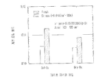
도 3은 게이트 재산화 방법에 따른 게이트전압에 따른 전류밀도 그래프. 3 is a current density graph according to a gate voltage according to a gate reoxidation method.
도 4는 게이트 재산화 방법에 따른 계면 트랩밀도 그래프. 4 is an interfacial trap density graph according to a gate reoxidation method.
도 5a 내지 도 5g는 본 발명에 따른 반도체소자의 제조공정도.Figures 5a to 5g is a manufacturing process of the semiconductor device according to the present invention.
도 6은 도 5a 상태의 레이아웃도. 6 is a layout diagram of the state of FIG. 5A;
<도면의 주요 부분에 대한 부호의 설명> <Explanation of symbols for the main parts of the drawings>
10, 40 : 반도체기판 12, 42 : 소자분리막10, 40:
14, 44 : 터널산화막 16, 46 : 제1다결정실리콘층14, 44
18, 48 : 게이트간 절연막 20, 50 : 제2다결정실리콘층18, 48: inter-gate
22 : 확산방지막 24, 70 : W층22:
26, 56 : 하드마스크층 28, 58 : 감광막 패턴26, 56:
30, 60 : 재산화막 32, 62 : 스페이서30, 60:
34, 64 : 소오스/드레인영역 36, 66 : 층간절연막34, 64 source /
52 : 희생산화막 54 : 제3다결정실리콘층52
68 : 확산방지막68: diffusion barrier
본 발명은 반도체소자의 제조방법에 관한 것으로서, 특히 다결정실리콘/금속 적층 구조의 조절 게이트를 사용하는 플레쉬 메모리 소자에서 금속층을 다마신 공정으로 게이트 재산화 공정 후에 형성하여 자유로운 금속 사용이 가능하고, 금속과 다결정실리콘층 계면간의 반응이 최소화되어 RC 지연이 감소되어 소자의 고속동작이 가능하여 공정수율 및 소자 동작의 특성을 향상시킬 수 있는 반도체소자의 제조방법에 관한 것이다. BACKGROUND OF THE INVENTION 1. Field of the Invention The present invention relates to a method for manufacturing a semiconductor device. In particular, in a flash memory device using a control gate of a polysilicon / metal stacked structure, a metal layer is formed after a gate reoxidation process by a damascene process, and free metal can be used. The present invention relates to a method for fabricating a semiconductor device capable of minimizing the reaction between the polysilicon layer interface and reducing the RC delay to enable high-speed operation of the device, thereby improving process yield and device operation characteristics.
최근의 반도체 장치의 고집적화 추세는 미세 패턴 형성 기술의 발전에 큰 영향을 받고 있으며, 반도체 장치의 제조 공정 중에서 식각 또는 이온주입 공정 등의 마스크로 매우 폭 넓게 사용되는 감광막 패턴의 미세화가 필수 요건이다. The recent trend of high integration of semiconductor devices has been greatly influenced by the development of fine pattern formation technology, and the miniaturization of photoresist patterns, which are widely used as masks such as etching or ion implantation processes, are essential in the manufacturing process of semiconductor devices.
이러한 감광막 패턴의 분해능(R)은 감광막 자체의 재질이나 기판과의 접착력 등과도 밀접한 연관이 있으나, 일차적으로는 사용되는 축소노광장치의 광원 파장(??) 및 공정 변수(k)에 비례하고, 노광 장치의 렌즈 구경(numerical aperture; NA, 개구수)에 반비례한다. The resolution (R) of the photoresist pattern is closely related to the material of the photoresist itself or the adhesion to the substrate, but is primarily proportional to the light source wavelength (??) and the process variable (k) of the reduction exposure apparatus used. It is inversely proportional to the lens aperture (NA, numerical aperture) of the exposure apparatus.
여기서 상기 축소노광장치의 광분해능을 향상시키기 위하여 광원의 파장을 감소시키게 되며, 예를 들어 파장이 436 및 365㎚인 G-라인 및 i-라인 축소노광장치는 공정 분해능이 라인/스페이스 패턴의 경우 각각 약 0.7, 0.5㎛ 정도가 한계이 고, 0.5㎛ 이하의 미세 패턴을 형성하기 위해서는 이보다 파장이 더 작은 원자외선(deep ultra violet; DUV), 예를 들어 파장이 248㎚인 KrF 레이저나 193㎚인 ArF 레이저를 광원으로 사용하는 노광 장치를 이용하여야 한다. Here, the wavelength of the light source is reduced to improve the optical resolution of the reduced exposure apparatus. For example, the G-line and i-line reduced exposure apparatus having wavelengths of 436 and 365 nm have a process resolution of a line / space pattern. In order to form a fine pattern of 0.5 μm or less, a deep ultra violet (DUV) or a KrF laser having a wavelength of 248 nm or 193 nm is used to form a fine pattern of 0.5 μm or less, respectively. An exposure apparatus using an ArF laser as a light source should be used.
또한 축소노광장치와는 별도로 공정 상의 방법으로는 노광마스크(photo mask)로서 위상반전마스크(phase shift mask)를 사용하는 방법이나, 이미지 콘트라스트를 향상시킬 수 있는 별도의 박막을 웨이퍼 상에 형성하는 씨.이.엘(contrast enhancement layer; CEL) 방법이나, 두층의 감광막 사이에 에스.오.지(spin on glass; SOG)등의 중간층을 개재시킨 삼층레지스트(Tri layer resister; 이하 TLR이라 칭함) 방법 또는 감광막의 상측에 선택적으로 실리콘을 주입시키는 실리레이션 방법 등이 개발되어 분해능 한계치를 낮추고 있다. In addition to the reduction exposure apparatus, the process method includes a method of using a phase shift mask as a photo mask, or forming a separate thin film on the wafer to improve image contrast. A contrast enhancement layer (CEL) method or a tri layer resister (hereinafter referred to as a TLR) method in which an intermediate layer such as spin on glass (SOG) is interposed between two photoresist layers. In addition, a silicide method for selectively injecting silicon into the upper side of the photosensitive film has been developed to lower the resolution limit.
또한 반도체소자가 고집적화되어 감에 따라 소자의 크기를 감소시키기 위하여 모스 전계효과 트랜지스터(Metal Oxide Semi conductor Field Effect Transistor; 이하 MOS FET라 칭함)의 게이트전극이나 소오스/드레인영역 및 이들과의 콘택등 공정 전반의 디자인 룰이 감소되고 있으나, 게이트전극의 폭과 전기저항은 비례 관계에 있어 폭이 N배 줄어들면 전기 저항이 N배 증가되어 반도체소자의 동작 속도를 떨어뜨리는 문제점이 있다. 따라서 게이트전극의 저항을 감소시키기 위하여 가장 안정적인 MOSFET 특성을 나타내는 다결정실리콘층/산화막 계면의 특성을 이용하여 다결정실리콘층과 실리사이드의 적층 구조인 폴리사이드가 저 저항 게이트로서 사용하기도 한다. In addition, in order to reduce the size of the semiconductor device as the semiconductor device is highly integrated, a process such as a gate electrode, a source / drain region, and a contact thereof with a metal oxide semi-conductor field effect transistor (hereinafter referred to as a MOS FET) Although the overall design rule is reduced, there is a problem in that the width of the gate electrode and the electrical resistance are proportional to each other, so that if the width is reduced by N times, the electrical resistance is increased by N times to reduce the operation speed of the semiconductor device. Therefore, in order to reduce the resistance of the gate electrode, polyside, which is a laminated structure of the polysilicon layer and the silicide, may be used as the low resistance gate by using the property of the polysilicon layer / oxide layer interface that exhibits the most stable MOSFET characteristics.
종래 0.1㎛ 이하의 게이트 선폭을 가지는 h집적 비휘발성 플레쉬 메모리 소 자는 W-폴리사이드 적층 구조의 조절 게이트를 사용하면 저항이 증가되어 저항이 상대적으로 낮은 W/WNx/다결정실리콘층 적층 구조를 사용한다.Conventionally, the h-integrated nonvolatile flash memory device having a gate line width of 0.1 μm or less uses a W / WNx / polycrystalline silicon layer structure having relatively low resistance due to an increase in resistance when a control gate having a W-polyside stack structure is used. .
도 1a 내지 도 1e는 종래 기술에 따른 반도체소자의 제조 공정도로서, 도2와 연계시켜 설명한다. 도2는 도 1b 상태에서의 레이아웃도로서, 상기 도 1a 및 도 1b는 도 2에서의 선 Ⅰ-Ⅰ에 따른 단면 상태의 공정 진행도이고, 도 1c 및 도 1d 는 도 2에서의 선 Ⅱ-Ⅱ에 따른 단면 상태의 공정 진행도이다. 1A to 1E are manufacturing process diagrams of a semiconductor device according to the prior art, which will be described with reference to FIG. 2. FIG. 2 is a layout diagram in the state of FIG. 1B, wherein FIGS. 1A and 1B are process progress diagrams in a cross-sectional state along the line I-I in FIG. 2, and FIGS. 1C and 1D are line II- in FIG. 2. The process progression of the cross-sectional state by II.
도 1a를 참조하면, 실리콘 웨이퍼의 반도체기판(10)상에 얕은 트랜치 공정을 이용하여 스트라이프 형상의 소자분리막(12)을 형성하고, 반도체기판(10)상에 터널산화막(14)을 형성한 후, 상기 터널산화막(14)상에 부유게이트가 되는 제1다결정실리콘층(16) 패턴을 형성한다. Referring to FIG. 1A, a stripe-type
도 1b를 참조하면, 상기 구조의 전표면에 산화막-질화막-산화막 구조의 게이트간 절연막(18)을 도포하고, 상기 게이트간 절연막(18) 상에 조절게이트가 되는 제2다결정실리콘층(20)과 W-N 또는 W-Si-N 재질의 확산방지막(22) 및 게이트용 W층(24)을 순차적으로 형성한다. Referring to FIG. 1B, an inter-gate
도 1c를 참조하면, 상기 W층(24)상에 하드마스크층(26)을 도포하고, 상기 하드마스크층(26)상에 부유게이트 패턴닝용의 감광막 패턴(28)을 형성한다. Referring to FIG. 1C, a
도 1d를 참조하면, 상기 감광막 패턴(28)을 마스크로 하드마스크층(26)에서 제1다결정실리콘층(16)까지 순차적으로 식각하여 섬형상의 제1다결정실리콘층(16) 패턴으로된 부유게이트를 형성하고, 그 상부에 중첩되어 있는 제2다결정실리콘층(20) 및 W층(24) 패턴을 형성한다. Referring to FIG. 1D, the
그 후, 상기 구조의 반도체기판(10)을 O2 분위기에서 게이트 재산화 공정을 진행하거나, H2O 와 H2 혼합분위기에서 게이트 선택적 재산화 공정을 진행하여 상기 다결정실리콘층들(16),(20)의 측벽에 재산화막(30)을 형성한다. 여기서 상기 재산화 공정은 게이트 식각후 플라즈마 손상을 보상하기 위한 공정으로서, 이때 게이트 에지 부분에 게이트 버즈빅 산화가 일어난다. Thereafter, the
도 1e를 참조하면, 상기 제1다결정실리콘층(16) 패턴에서 W층(24) 패턴까지의 측벽에 스페이서(32)를 형성하고, 상기 패턴들 양측의 반도체기판(10)에 소오스/드레인영역(34)을 형성한 후, 상기 구조의 전표면에 층간절연막(36)을 도포하고, 화학-기계적 연마(Chemical-Mechanical Polishing: 이하 CMP라 칭함)나 에치백 등의 방법으로 상기 층간절연막(36)의 상부를 제거하여 상기 W층(24) 상부를 노출시킨다. Referring to FIG. 1E,
상기한 바와 같이, 종래 기술에 따른 반도체소자의 제조방법은 W/WNx/다결정실리콘층/게이트간 절연막/다결정실리콘층의 적층 게이트를 패턴닝한 후, 플라즈마에 의한 손상을 보상하기 위하여 게이트 재산화 공정을 진행한다. As described above, in the method of manufacturing a semiconductor device according to the prior art, after patterning the laminated gate of the W / WNx / polycrystalline silicon layer / inter-gate insulating film / polycrystalline silicon layer, gate re-oxidation to compensate for damage by plasma Proceed with the process.
이때 W층이 외부에 노출되어 W의 이상산화를 방지하기 위하여 기존의 건식 O2 방식의 게이트 재산화 공정 대신에 H2O/H2 혼합가스 분위기에서 선택적 게이트재산화 공정을 진행하게 된다. At this time, the W layer is exposed to the outside, and in order to prevent abnormal oxidation of W, instead of the conventional dry O2 gate reoxidation process, a selective gate reoxidation process is performed in an H 2 O /
그러나 게이트 재산화 공정은 도 3에 도시되어 있는 바와 같이, 선택적 게이트 재산화 공정은 게이트 재산화 공정 보다 게이트 산화막의 스트레스 유도 누설전류의 특성을 악화시키고, 도 4에서와 같이, 계면 트랩 밀도가 선택적 게이트 재산 화 공정은 게이트 재산화 공정 보다 증가되는 문제점이 있다. However, as the gate reoxidation process is shown in FIG. 3, the selective gate reoxidation process worsens the characteristics of the stress induced leakage current of the gate oxide film than the gate reoxidation process, and as shown in FIG. 4, the interface trap density is selective. The gate reoxidation process has an increased problem than the gate reoxidation process.
또한 종래 기술에서 고온에서 실시하는 선택적 게이트 재산화 공정 중에 W층과 다결정실리콘층의 계면에 Si-N 및 Si-O 본드가 형성되며, Si-N 본드는 확산방지 역할을 하므로 특성에 영향을 미치지 않으나, Si-O 본드는 선택적 재산화 공정시 O2 또는 H2O가 W층을 통과하여 계면에 이르러 형성되는 것으로서 고속 동작 소자의 RC 지연을 유발시키는 문제점이 있다. In addition, Si-N and Si-O bonds are formed at the interface between the W layer and the polysilicon layer during the selective gate reoxidation process performed at a high temperature in the prior art, and the Si-N bonds do not affect properties because they act as diffusion barriers. However, the Si-O bond is formed as O2 or H2O is formed to reach the interface through the W layer during the selective reoxidation process, causing the RC delay of the high-speed operating device.
본 발명은 상기와 같은 문제점을 해결하기 위한 것으로서, 본 발명의 목적은 간단한 공정상의 변화로 W층을 다마신 방법으로 형성하여 게이트 재산화 공정에 의한 소자의 특성 저하를 방지하여 공정수율 및 소자의 신뢰성을 향상시킬 수 있는 반도체소자의 제조방법을 제공함에 있다. The present invention is to solve the above problems, the object of the present invention is to form a W layer by the damascene method by a simple process change to prevent the deterioration of the characteristics of the device by the gate reoxidation process process yield and It is to provide a method of manufacturing a semiconductor device that can improve the reliability.
상기와 같은 목적을 달성하기 위한 본 발명에 따른 반도체소자 제조방법의 특징은,Features of the semiconductor device manufacturing method according to the present invention for achieving the above object,
반도체기판상에 스트라이프 형상의 소자분리막을 형성하는 공정과, Forming a stripe-shaped device isolation film on the semiconductor substrate;
상기 반도체기판상에 터널산화막을 형성하는 공정과, Forming a tunnel oxide film on the semiconductor substrate;
상기 터널산화막 상에 제1다결정실리콘층 패턴을 형성하는 공정과, Forming a first polysilicon layer pattern on the tunnel oxide film;
상기 구조의 전표면에 게이트간 절연막과, 제2다결정실리콘층, 희생산화막 및 제3다결정실리콘층을 순차적으로 형성하는 공정과, Sequentially forming an inter-gate insulating film, a second polysilicon layer, a sacrificial oxide film, and a third polysilicon layer on the entire surface of the structure;
상기 제3다결정실리콘층에서 제1다결정실리콘층까지를 게이트 패턴닝용 마스 크를 사용하여 패턴닝하여 섬형상의 부유게이트인 제1다결정실리콘층 패턴과, 제2 및 제3다결정실리콘층 패턴을 형성하는 공정과, Patterning the third polysilicon layer to the first polysilicon layer using a mask for gate patterning to form a first polycrystalline silicon layer pattern as an island-shaped floating gate, and second and third polysilicon layer patterns Process to do,
상기 구조의 반도체기판을 게이트 재산화 공정을 진행하여 상기 제1 내지 제3다결정실리콘층 패턴들의 표면에 재산화막을 형성하는 공정과, Forming a reoxidation film on the surfaces of the first to third polysilicon layer patterns by performing a gate reoxidation process on the semiconductor substrate having the structure;
상기 패턴들의 측벽에 스페이서를 형성하는 공정과, Forming a spacer on sidewalls of the patterns;
상기 패턴들 사이를 층간절연막으로 채우는 공정과, Filling the gaps between the patterns with an interlayer insulating film;
상기 제3다결정실리콘층 패턴과 희생산화막을 제거하여 제2다결정실리콘층을 노출시키는 공정과, Exposing the second polycrystalline silicon layer by removing the third polysilicon layer pattern and the sacrificial oxide film;
상기 제3다결정실리콘층이 제거된 홈을 금속층으로 메우는 공정을 구비함에 있다. And filling the grooves from which the third polysilicon layer is removed with a metal layer.
또한 본 발명의 다른 특징은, 상기 게이트간 절연막은 산화막, 질화막 또는 산화막-질화막-산화막 적층 구조로 형성되거나, Hf, Zr, Al, Ce 또는 Ta을 포함하는 금속산화물, 금속질화산화물 또는 금속질화실리케이트로 형성된다. In another aspect of the present invention, the inter-gate insulating film may be formed of an oxide film, a nitride film, or an oxide film-nitride film-oxide stacked structure, or a metal oxide, metal nitride oxide, or metal nitride including Hf, Zr, Al, Ce, or Ta. Is formed.
또한 본 발명의 또 다른 특징은, 상기 게이트 재산화 공정은 O2 또는 H2O 분위기에서 700-1100℃에서 열처리하거나, O2를 포함하는 분위기에서 100-700℃에서 플라즈마 처리하며, 상기 게이트 재산화 공정시 게이트 버즈빅 산화가 일어난다. In still another aspect of the present invention, the gate reoxidation process is heat-treated at 700-1100 ° C. in an
또한 상기 스페이서는 산화막, 질화막 또는 그 적층막 구조로 이루어지며, 상기 금속층은 W, Mo, Ta, Co, Ti, Cu 또는 Pt로 형성되고, 상기 금속층 형성 공정 전에 확산방지막을 형성하는 공정을 구비하는 것을 특징으로 한다. In addition, the spacer is formed of an oxide film, a nitride film or a laminated film structure, wherein the metal layer is formed of W, Mo, Ta, Co, Ti, Cu or Pt, and comprises a step of forming a diffusion barrier film before the metal layer forming process It is characterized by.
또한 상기 확산방지막은 10-100Å 두께로 형성하고, 상기 확산방지막은 금속 잴화막 재질로서 WNx, MoNx, TiNx, HfNx, TaNx, W-Si-N, Ti-Si-N, Ti-Al-N 또는 Ta-Si-N (x = 0.05-2.0)으로 형성되며, 상기 확산방지막으로 금속질화막의 하부에 10-50Å두께의 W, Mo, Ti, Hf, Ta, WSix, MoSix, TiSix, HfSix 또는 TaSix (x = 0.05-2.0) 막을 추가로 삽입시켜 이중 확산방지막을 형성시키는 것을 특징으로 한다. In addition, the diffusion barrier is formed in a thickness of 10-100Å, the diffusion barrier is a metal nitride film material WNx, MoNx, TiNx, HfNx, TaNx, W-Si-N, Ti-Si-N, Ti-Al-N or It is formed of Ta-Si-N (x = 0.05-2.0), and the diffusion barrier layer is W, Mo, Ti, Hf, Ta, WSix, MoSix, TiSix, HfSix or TaSix (10-50Å thick at the bottom of the metal nitride film) x = 0.05-2.0) is further inserted to form a double diffusion barrier.
이하, 첨부된 도면을 참조하여 본 발명에 따른 반도체소자의 제조방법에 대하여 상세히 설명을 하기로 한다. Hereinafter, a method of manufacturing a semiconductor device according to the present invention will be described in detail with reference to the accompanying drawings.
도 5a 내지 도 5g는 본 발명에 따른 반도체소자의 제조공정도로서, 비휘발성 플레쉬 소자의 예이며, 도 6과 연계시켜 설명한다. 여기서 도 6은 도 5a 상태에서의 레이아웃도로서, 상기 도 5는 도 6에서의 선 Ⅲ-Ⅲ에 따른 단면 상태의 공정 진행도이고, 도 5b 내지 도 5g 는 도 6에서의 선 Ⅳ-Ⅳ에 따른 단면 상태의 공정 진행도이다. 5A to 5G are manufacturing process diagrams of a semiconductor device according to the present invention, which is an example of a nonvolatile flash device, and will be described with reference to FIG. 6. FIG. 6 is a layout diagram in a state of FIG. 5A, where FIG. 5 is a process progress diagram in a cross-sectional state along the line III-III in FIG. 6, and FIGS. 5B to 5G are in line IV-IV in FIG. 6. The process progress of the cross-sectional state along.
도 5a를 참조하면, 실리콘 웨이퍼 등의 반도체기판(40)상에 얕은 트랜치 공정을 진행하여 스트라이프 형상의 소자분리막(42)을 형성하고, 웰 및 채널 이온주입 공정을 진행한 후, 반도체기판(40)상에 플레쉬 소자의 터널산화막(44)을 형성하고, 상기 터널산화막(44)상에 부유게이트가 되는 제1다결정실리콘층(46) 패턴을 다결정실리콘층 도포 및 사진 식각 공정을 진행하여 상기 소자분리막(42)과 평행한 스트라이프 형상으로 형성한다. Referring to FIG. 5A, a shallow trench process may be performed on a
그다음 상기 구조의 전표면에 소정재질, 예를 들어 산화막이나 질화막 또는 산화막-질화막-산화막 적층 구조의 게이트간 절연막(48)을 도포하고, 상기 게이트 간 절연막(48) 상에 조절게이트가 되는 제2다결정실리콘층(50)을 도포하여 평탄화 시킨 후, 상기 제2다결정실리콘층(50)상에 희생산화막(52)과 제3다결정실리콘층(54)을 순차적으로 형성한다. 여기서 상기 게이트간 절연막(48)은 Hf, Zr, Al, Ce 또는 Ta을 포함하는 금속산화물, 금속질화산화물 또는 금속질화실리케이트 등의 고유전상수 유전막을 사용할 수도 있다. Then, a second material serving as a control gate on the inter-gate insulating
도 5b를 참조하면, 상기 제3다결정실리콘층(54)상에 하드마스크층(56)을 도포하고, 상기 하드마스크층(56)상에 부유게이트 패턴닝용의 감광막 패턴(58)을 형성한다. Referring to FIG. 5B, a
도 5c를 참조하면, 상기 감광막 패턴(58)을 마스크로 하드마스크층(56)에서 제1다결정실리콘층(56)까지 순차적으로 식각하여 섬형상의 부유게이트인 제1다결정실리콘층(46) 패턴과, 제2 및 제3다결정실리콘층(50),(54) 패턴을 형성하고, 남아있는 감광막 패턴(58)과 하드마스크층(56)을 제거한다. Referring to FIG. 5C, the
도 5d를 참조하면, 상기 구조의 반도체기판(40)을 O2 또는 H2O 분위기에서 게이트 재산화 공정을 700-1100℃에서 열처리하거나, 산소가 포함된 분위기에서 100-700℃에서 플라즈마 처리하는 공정을 진행하여 상기 패턴들의 노출된 표면에 재산화막(60)을 형성한다. 여기서 상기 재산화 공정은 게이트 식각후 플라즈마 손상을 보상하기 위한 공정으로서, 이때 게이트 에지 부분에 게이트 버즈빅 산화가 일어난다. Referring to FIG. 5D, the
도 5e를 참조하면, 상기 구조의 전표면에 게이트 스페이서 물질, 예를 들어 산화막, 질화막 또는 그 적층막 구조의 물질을 증착하고, 이를 제3다결정실리콘층 (54) 패턴의 상부면이 노출될 때까지 에치백하여 상기 패턴들의 측벽 재산화막(60)의 외곽에 스페이서(62)를 형성한다. Referring to FIG. 5E, a gate spacer material, for example, an oxide film, a nitride film, or a laminated film structure, is deposited on the entire surface of the structure, and the upper surface of the
그다음 상기 제3다결정실리콘층(56) 양측의 반도체기판(40)에 불순물을 이온주입하여 소오스/드레인영역(64)을 형성하고, 상기 구조의 전표면에 층간절연막(66)을 형성한 후, 에치백이나 CMP 등의 방법으로 상부를 평탄화시켜 상기 제3다결정실리콘층(54)의 상부를 노출시킨다. Then, source / drain regions 64 are formed by ion implantation of impurities into the
도 5f를 참조하면, 다마신 공정을 진행하기 위하여 상기 노출된 제3다결정실리콘층(54) 패턴과 희생산화막(52)을 제거하여 제2다결정실리콘층(50)을 노출시킨 후, 상기 구조의 전표면에 금속질화막 재질의 확산방지막(68)과 조절 게이트가 되는 W층(70)을 순차적으로 형성한다. 여기서 상기 확산방지막(68)은 WNx, MoNx, TiNx, HfNx, TaNx, W-Si-N, Ti-Si-N, Ti-Al-N 또는 Ta-Si-N을 사용할 수 있으며,x는 0.05-2.00의 값을 가지는 10-100Å 정도 두께로 형성한다. 또한 제2다결정실리콘층(50)과 확산방지마(68)의 계면에 Si-N와 같은 절연막이 형성되는 것을 방지하기 위하여 상기 금속질화막 재지의 확산방지막(68) 하부에 10-50Å 두께의 W, Mo, Ti, Hf, Ta 또는 WSix, MoSix, TiSix, HfSix, TaSix (x = 0.05-2.0) 막을 추가로 형성하여 이중확산방지막으로 형성할 수도 있다. 또한 W층(70) 형성 후에 진행되는 후속 공정에서 열공정 온도가 600℃ 이하인 경우에는 W과 다결정실리콘층간의 확산이 거의 일어나지 않으므로 상기 확산방지막(68)을 형성하지 않을 수도 있다. Referring to FIG. 5F, the second
도 5g를 참조하면, 상기 층간절연막(66)상의 W층(70)과 확산방지막(68)을 순차적으로 CMP 또는 에치백 등의 방법으로 제거하여 상기 제3다결정실리콘층(54)이 제거된 부분에만 W층(70) 패턴이 남도록 한다. 여기서 본 발명에 따른 플레쉬 메모리 소자는 게이트 재산화 공정에서의 터널산화막과 게이트간 산화막의 열화가 일어나지 않으므로 상기 W층(70)을 W, Mo, Ta, Co, Ti, Cu 또는 Pt 등과 같이 공정 가능한 거의 모든 금속을 사용할 수 있다. Referring to FIG. 5G, a portion of the
이상에서 설명한 바와 같이 본 발명에 따른 반도체소자의 제조방법은 다결정실리콘/금속 적층 구조의 조절 게이트를 사용하는 플레쉬 메모리 소자에서 금속층을 다마신 공정으로 게이트 재산화 공정 후에 형성하였으므로, 게이트 재산화 공정에서 금속층을 통한 확산에 의한 터널산화막 및 게이트간 산화막의 열화가 일어나지 않으므로 공정 가능한 거의 모든 금속을 사용할 수 있어 공정상의 여유도가 증가되고, 고온의 게이트 재산화와 소오스/드레인영역 열처리 공정이 금속 게이트 형성 전에 실시되므로, 금속과 다결정실리콘층 계면간의 반응이 최소화되어 RC 지연이 감소되어 소자의 고속동작이 가능하여 공정수율 및 소자 동작의 특성을 향상시킬 수 있는 이점이 있다.
As described above, in the method of manufacturing a semiconductor device according to the present invention, since a metal layer is formed after a gate reoxidation process by a damascene process in a flash memory device using a control gate of a polysilicon / metal stacked structure, Since the tunnel oxide film and the gate oxide film do not deteriorate due to diffusion through the metal layer, almost any metal that can be processed can be used to increase the process margin, and the high temperature gate reoxidation and the source / drain region heat treatment process form the metal gate. Since it is performed before, the reaction between the metal and the polysilicon layer interface is minimized, so that the RC delay is reduced, so that the device can be operated at high speed, thereby improving process yield and device operation characteristics.
Claims (12)
Priority Applications (1)
| Application Number | Priority Date | Filing Date | Title |
|---|---|---|---|
| KR1020040076971A KR100573838B1 (en) | 2004-09-24 | 2004-09-24 | Method for fabricating semiconductor device |
Applications Claiming Priority (1)
| Application Number | Priority Date | Filing Date | Title |
|---|---|---|---|
| KR1020040076971A KR100573838B1 (en) | 2004-09-24 | 2004-09-24 | Method for fabricating semiconductor device |
Publications (2)
| Publication Number | Publication Date |
|---|---|
| KR20060028001A true KR20060028001A (en) | 2006-03-29 |
| KR100573838B1 KR100573838B1 (en) | 2006-04-27 |
Family
ID=37138863
Family Applications (1)
| Application Number | Title | Priority Date | Filing Date |
|---|---|---|---|
| KR1020040076971A Expired - Fee Related KR100573838B1 (en) | 2004-09-24 | 2004-09-24 | Method for fabricating semiconductor device |
Country Status (1)
| Country | Link |
|---|---|
| KR (1) | KR100573838B1 (en) |
Cited By (3)
| Publication number | Priority date | Publication date | Assignee | Title |
|---|---|---|---|---|
| KR100809328B1 (en) * | 2006-07-19 | 2008-03-05 | 삼성전자주식회사 | Method for manufacturing nonvolatile memory integrated circuit device and nonvolatile memory integrated circuit device manufactured through the same |
| WO2010078189A3 (en) * | 2008-12-31 | 2010-09-16 | Intel Corporation | Flash cell with integrated high-k dielectric and metal-based control gate |
| US9818719B2 (en) | 2010-06-30 | 2017-11-14 | Intel Corporation | Bumpless build-up layer package design with an interposer |
-
2004
- 2004-09-24 KR KR1020040076971A patent/KR100573838B1/en not_active Expired - Fee Related
Cited By (4)
| Publication number | Priority date | Publication date | Assignee | Title |
|---|---|---|---|---|
| KR100809328B1 (en) * | 2006-07-19 | 2008-03-05 | 삼성전자주식회사 | Method for manufacturing nonvolatile memory integrated circuit device and nonvolatile memory integrated circuit device manufactured through the same |
| US7535052B2 (en) | 2006-07-19 | 2009-05-19 | Samsung Electronics Co., Ltd. | Method of fabricating non-volatile memory integrated circuit device and non-volatile memory integrated circuit device fabricated using the same |
| WO2010078189A3 (en) * | 2008-12-31 | 2010-09-16 | Intel Corporation | Flash cell with integrated high-k dielectric and metal-based control gate |
| US9818719B2 (en) | 2010-06-30 | 2017-11-14 | Intel Corporation | Bumpless build-up layer package design with an interposer |
Also Published As
| Publication number | Publication date |
|---|---|
| KR100573838B1 (en) | 2006-04-27 |
Similar Documents
| Publication | Publication Date | Title |
|---|---|---|
| KR100546378B1 (en) | Method for manufacturing a transistor having a recess channel | |
| US7528031B2 (en) | Semiconductor device and method for manufacturing the same | |
| CN112635401A (en) | Method for forming transistor | |
| JP4556293B2 (en) | Capacitor manufacturing method for semiconductor device | |
| KR100350764B1 (en) | Manufacturing method of semiconductor device | |
| KR100573838B1 (en) | Method for fabricating semiconductor device | |
| US7300883B2 (en) | Method for patterning sub-lithographic features in semiconductor manufacturing | |
| KR20100108715A (en) | Method for manufacturing of non-volatile memory device | |
| KR20030075745A (en) | Method of Forming Metal Gate in Semiconductor Device | |
| TWI905536B (en) | Semiconductor device and method fabricating the same | |
| TWI899484B (en) | Method of manufacturing semiconductor structure | |
| KR100576461B1 (en) | Manufacturing method of semiconductor device | |
| US7071085B1 (en) | Predefined critical spaces in IC patterning to reduce line end pull back | |
| KR20050034292A (en) | Manufacturing method for semiconductor device | |
| KR100944344B1 (en) | Manufacturing method of semiconductor device | |
| KR100744086B1 (en) | Manufacturing method of semiconductor device | |
| KR20030051036A (en) | Transistor in a semiconductor device and method of manufacturing thereof | |
| KR100527531B1 (en) | Manufacturing method for semiconductor device | |
| KR101204662B1 (en) | Method for fabricating transistor in semiconductor device | |
| KR100687874B1 (en) | Method of forming recess channel in semiconductor device | |
| KR100418923B1 (en) | method for fabricating semiconductor device | |
| KR20060114432A (en) | Manufacturing method of semiconductor device | |
| KR20070115353A (en) | Pattern formation method of semiconductor device and cell pattern formation method of nonvolatile memory using same | |
| KR20050014156A (en) | Manufacturing method for semiconductor device | |
| KR20060114433A (en) | Manufacturing method of semiconductor device |
Legal Events
| Date | Code | Title | Description |
|---|---|---|---|
| A201 | Request for examination | ||
| PA0109 | Patent application |
St.27 status event code: A-0-1-A10-A12-nap-PA0109 |
|
| PA0201 | Request for examination |
St.27 status event code: A-1-2-D10-D11-exm-PA0201 |
|
| PG1501 | Laying open of application |
St.27 status event code: A-1-1-Q10-Q12-nap-PG1501 |
|
| E701 | Decision to grant or registration of patent right | ||
| PE0701 | Decision of registration |
St.27 status event code: A-1-2-D10-D22-exm-PE0701 |
|
| GRNT | Written decision to grant | ||
| PR0701 | Registration of establishment |
St.27 status event code: A-2-4-F10-F11-exm-PR0701 |
|
| PR1002 | Payment of registration fee |
St.27 status event code: A-2-2-U10-U11-oth-PR1002 Fee payment year number: 1 |
|
| PG1601 | Publication of registration |
St.27 status event code: A-4-4-Q10-Q13-nap-PG1601 |
|
| PR1001 | Payment of annual fee |
St.27 status event code: A-4-4-U10-U11-oth-PR1001 Fee payment year number: 4 |
|
| PR1001 | Payment of annual fee |
St.27 status event code: A-4-4-U10-U11-oth-PR1001 Fee payment year number: 5 |
|
| FPAY | Annual fee payment |
Payment date: 20110325 Year of fee payment: 6 |
|
| PR1001 | Payment of annual fee |
St.27 status event code: A-4-4-U10-U11-oth-PR1001 Fee payment year number: 6 |
|
| PN2301 | Change of applicant |
St.27 status event code: A-5-5-R10-R13-asn-PN2301 St.27 status event code: A-5-5-R10-R11-asn-PN2301 |
|
| LAPS | Lapse due to unpaid annual fee | ||
| PC1903 | Unpaid annual fee |
St.27 status event code: A-4-4-U10-U13-oth-PC1903 Not in force date: 20120419 Payment event data comment text: Termination Category : DEFAULT_OF_REGISTRATION_FEE |
|
| PN2301 | Change of applicant |
St.27 status event code: A-5-5-R10-R13-asn-PN2301 St.27 status event code: A-5-5-R10-R11-asn-PN2301 |
|
| PC1903 | Unpaid annual fee |
St.27 status event code: N-4-6-H10-H13-oth-PC1903 Ip right cessation event data comment text: Termination Category : DEFAULT_OF_REGISTRATION_FEE Not in force date: 20120419 |
|
| PN2301 | Change of applicant |
St.27 status event code: A-5-5-R10-R13-asn-PN2301 St.27 status event code: A-5-5-R10-R11-asn-PN2301 |
|
| P22-X000 | Classification modified |
St.27 status event code: A-4-4-P10-P22-nap-X000 |
|
| P22-X000 | Classification modified |
St.27 status event code: A-4-4-P10-P22-nap-X000 |
|
| P22-X000 | Classification modified |
St.27 status event code: A-4-4-P10-P22-nap-X000 |