KR102830409B1 - Display device having a constant current setting configuration and its driving method - Google Patents
Display device having a constant current setting configuration and its driving method Download PDFInfo
- Publication number
- KR102830409B1 KR102830409B1 KR1020207037474A KR20207037474A KR102830409B1 KR 102830409 B1 KR102830409 B1 KR 102830409B1 KR 1020207037474 A KR1020207037474 A KR 1020207037474A KR 20207037474 A KR20207037474 A KR 20207037474A KR 102830409 B1 KR102830409 B1 KR 102830409B1
- Authority
- KR
- South Korea
- Prior art keywords
- transistor
- control unit
- light
- constant current
- terminal
- Prior art date
- Legal status (The legal status is an assumption and is not a legal conclusion. Google has not performed a legal analysis and makes no representation as to the accuracy of the status listed.)
- Active
Links
Images


Classifications
-
- G—PHYSICS
- G09—EDUCATION; CRYPTOGRAPHY; DISPLAY; ADVERTISING; SEALS
- G09G—ARRANGEMENTS OR CIRCUITS FOR CONTROL OF INDICATING DEVICES USING STATIC MEANS TO PRESENT VARIABLE INFORMATION
- G09G3/00—Control arrangements or circuits, of interest only in connection with visual indicators other than cathode-ray tubes
- G09G3/20—Control arrangements or circuits, of interest only in connection with visual indicators other than cathode-ray tubes for presentation of an assembly of a number of characters, e.g. a page, by composing the assembly by combination of individual elements arranged in a matrix no fixed position being assigned to or needed to be assigned to the individual characters or partial characters
- G09G3/22—Control arrangements or circuits, of interest only in connection with visual indicators other than cathode-ray tubes for presentation of an assembly of a number of characters, e.g. a page, by composing the assembly by combination of individual elements arranged in a matrix no fixed position being assigned to or needed to be assigned to the individual characters or partial characters using controlled light sources
- G09G3/30—Control arrangements or circuits, of interest only in connection with visual indicators other than cathode-ray tubes for presentation of an assembly of a number of characters, e.g. a page, by composing the assembly by combination of individual elements arranged in a matrix no fixed position being assigned to or needed to be assigned to the individual characters or partial characters using controlled light sources using electroluminescent panels
- G09G3/32—Control arrangements or circuits, of interest only in connection with visual indicators other than cathode-ray tubes for presentation of an assembly of a number of characters, e.g. a page, by composing the assembly by combination of individual elements arranged in a matrix no fixed position being assigned to or needed to be assigned to the individual characters or partial characters using controlled light sources using electroluminescent panels semiconductive, e.g. using light-emitting diodes [LED]
-
- G—PHYSICS
- G09—EDUCATION; CRYPTOGRAPHY; DISPLAY; ADVERTISING; SEALS
- G09G—ARRANGEMENTS OR CIRCUITS FOR CONTROL OF INDICATING DEVICES USING STATIC MEANS TO PRESENT VARIABLE INFORMATION
- G09G3/00—Control arrangements or circuits, of interest only in connection with visual indicators other than cathode-ray tubes
- G09G3/20—Control arrangements or circuits, of interest only in connection with visual indicators other than cathode-ray tubes for presentation of an assembly of a number of characters, e.g. a page, by composing the assembly by combination of individual elements arranged in a matrix no fixed position being assigned to or needed to be assigned to the individual characters or partial characters
- G09G3/2007—Display of intermediate tones
- G09G3/2014—Display of intermediate tones by modulation of the duration of a single pulse during which the logic level remains constant
-
- G—PHYSICS
- G09—EDUCATION; CRYPTOGRAPHY; DISPLAY; ADVERTISING; SEALS
- G09G—ARRANGEMENTS OR CIRCUITS FOR CONTROL OF INDICATING DEVICES USING STATIC MEANS TO PRESENT VARIABLE INFORMATION
- G09G3/00—Control arrangements or circuits, of interest only in connection with visual indicators other than cathode-ray tubes
- G09G3/20—Control arrangements or circuits, of interest only in connection with visual indicators other than cathode-ray tubes for presentation of an assembly of a number of characters, e.g. a page, by composing the assembly by combination of individual elements arranged in a matrix no fixed position being assigned to or needed to be assigned to the individual characters or partial characters
- G09G3/2007—Display of intermediate tones
- G09G3/2018—Display of intermediate tones by time modulation using two or more time intervals
- G09G3/2022—Display of intermediate tones by time modulation using two or more time intervals using sub-frames
-
- G—PHYSICS
- G09—EDUCATION; CRYPTOGRAPHY; DISPLAY; ADVERTISING; SEALS
- G09G—ARRANGEMENTS OR CIRCUITS FOR CONTROL OF INDICATING DEVICES USING STATIC MEANS TO PRESENT VARIABLE INFORMATION
- G09G3/00—Control arrangements or circuits, of interest only in connection with visual indicators other than cathode-ray tubes
- G09G3/20—Control arrangements or circuits, of interest only in connection with visual indicators other than cathode-ray tubes for presentation of an assembly of a number of characters, e.g. a page, by composing the assembly by combination of individual elements arranged in a matrix no fixed position being assigned to or needed to be assigned to the individual characters or partial characters
- G09G3/22—Control arrangements or circuits, of interest only in connection with visual indicators other than cathode-ray tubes for presentation of an assembly of a number of characters, e.g. a page, by composing the assembly by combination of individual elements arranged in a matrix no fixed position being assigned to or needed to be assigned to the individual characters or partial characters using controlled light sources
- G09G3/30—Control arrangements or circuits, of interest only in connection with visual indicators other than cathode-ray tubes for presentation of an assembly of a number of characters, e.g. a page, by composing the assembly by combination of individual elements arranged in a matrix no fixed position being assigned to or needed to be assigned to the individual characters or partial characters using controlled light sources using electroluminescent panels
- G09G3/32—Control arrangements or circuits, of interest only in connection with visual indicators other than cathode-ray tubes for presentation of an assembly of a number of characters, e.g. a page, by composing the assembly by combination of individual elements arranged in a matrix no fixed position being assigned to or needed to be assigned to the individual characters or partial characters using controlled light sources using electroluminescent panels semiconductive, e.g. using light-emitting diodes [LED]
- G09G3/3208—Control arrangements or circuits, of interest only in connection with visual indicators other than cathode-ray tubes for presentation of an assembly of a number of characters, e.g. a page, by composing the assembly by combination of individual elements arranged in a matrix no fixed position being assigned to or needed to be assigned to the individual characters or partial characters using controlled light sources using electroluminescent panels semiconductive, e.g. using light-emitting diodes [LED] organic, e.g. using organic light-emitting diodes [OLED]
- G09G3/3225—Control arrangements or circuits, of interest only in connection with visual indicators other than cathode-ray tubes for presentation of an assembly of a number of characters, e.g. a page, by composing the assembly by combination of individual elements arranged in a matrix no fixed position being assigned to or needed to be assigned to the individual characters or partial characters using controlled light sources using electroluminescent panels semiconductive, e.g. using light-emitting diodes [LED] organic, e.g. using organic light-emitting diodes [OLED] using an active matrix
- G09G3/3233—Control arrangements or circuits, of interest only in connection with visual indicators other than cathode-ray tubes for presentation of an assembly of a number of characters, e.g. a page, by composing the assembly by combination of individual elements arranged in a matrix no fixed position being assigned to or needed to be assigned to the individual characters or partial characters using controlled light sources using electroluminescent panels semiconductive, e.g. using light-emitting diodes [LED] organic, e.g. using organic light-emitting diodes [OLED] using an active matrix with pixel circuitry controlling the current through the light-emitting element
-
- G—PHYSICS
- G09—EDUCATION; CRYPTOGRAPHY; DISPLAY; ADVERTISING; SEALS
- G09G—ARRANGEMENTS OR CIRCUITS FOR CONTROL OF INDICATING DEVICES USING STATIC MEANS TO PRESENT VARIABLE INFORMATION
- G09G3/00—Control arrangements or circuits, of interest only in connection with visual indicators other than cathode-ray tubes
- G09G3/20—Control arrangements or circuits, of interest only in connection with visual indicators other than cathode-ray tubes for presentation of an assembly of a number of characters, e.g. a page, by composing the assembly by combination of individual elements arranged in a matrix no fixed position being assigned to or needed to be assigned to the individual characters or partial characters
- G09G3/22—Control arrangements or circuits, of interest only in connection with visual indicators other than cathode-ray tubes for presentation of an assembly of a number of characters, e.g. a page, by composing the assembly by combination of individual elements arranged in a matrix no fixed position being assigned to or needed to be assigned to the individual characters or partial characters using controlled light sources
- G09G3/30—Control arrangements or circuits, of interest only in connection with visual indicators other than cathode-ray tubes for presentation of an assembly of a number of characters, e.g. a page, by composing the assembly by combination of individual elements arranged in a matrix no fixed position being assigned to or needed to be assigned to the individual characters or partial characters using controlled light sources using electroluminescent panels
- G09G3/32—Control arrangements or circuits, of interest only in connection with visual indicators other than cathode-ray tubes for presentation of an assembly of a number of characters, e.g. a page, by composing the assembly by combination of individual elements arranged in a matrix no fixed position being assigned to or needed to be assigned to the individual characters or partial characters using controlled light sources using electroluminescent panels semiconductive, e.g. using light-emitting diodes [LED]
- G09G3/3208—Control arrangements or circuits, of interest only in connection with visual indicators other than cathode-ray tubes for presentation of an assembly of a number of characters, e.g. a page, by composing the assembly by combination of individual elements arranged in a matrix no fixed position being assigned to or needed to be assigned to the individual characters or partial characters using controlled light sources using electroluminescent panels semiconductive, e.g. using light-emitting diodes [LED] organic, e.g. using organic light-emitting diodes [OLED]
- G09G3/3275—Details of drivers for data electrodes
- G09G3/3291—Details of drivers for data electrodes in which the data driver supplies a variable data voltage for setting the current through, or the voltage across, the light-emitting elements
-
- G—PHYSICS
- G09—EDUCATION; CRYPTOGRAPHY; DISPLAY; ADVERTISING; SEALS
- G09G—ARRANGEMENTS OR CIRCUITS FOR CONTROL OF INDICATING DEVICES USING STATIC MEANS TO PRESENT VARIABLE INFORMATION
- G09G2300/00—Aspects of the constitution of display devices
- G09G2300/08—Active matrix structure, i.e. with use of active elements, inclusive of non-linear two terminal elements, in the pixels together with light emitting or modulating elements
- G09G2300/0809—Several active elements per pixel in active matrix panels
- G09G2300/0819—Several active elements per pixel in active matrix panels used for counteracting undesired variations, e.g. feedback or autozeroing
-
- G—PHYSICS
- G09—EDUCATION; CRYPTOGRAPHY; DISPLAY; ADVERTISING; SEALS
- G09G—ARRANGEMENTS OR CIRCUITS FOR CONTROL OF INDICATING DEVICES USING STATIC MEANS TO PRESENT VARIABLE INFORMATION
- G09G2300/00—Aspects of the constitution of display devices
- G09G2300/08—Active matrix structure, i.e. with use of active elements, inclusive of non-linear two terminal elements, in the pixels together with light emitting or modulating elements
- G09G2300/0809—Several active elements per pixel in active matrix panels
- G09G2300/0842—Several active elements per pixel in active matrix panels forming a memory circuit, e.g. a dynamic memory with one capacitor
- G09G2300/0852—Several active elements per pixel in active matrix panels forming a memory circuit, e.g. a dynamic memory with one capacitor being a dynamic memory with more than one capacitor
-
- G—PHYSICS
- G09—EDUCATION; CRYPTOGRAPHY; DISPLAY; ADVERTISING; SEALS
- G09G—ARRANGEMENTS OR CIRCUITS FOR CONTROL OF INDICATING DEVICES USING STATIC MEANS TO PRESENT VARIABLE INFORMATION
- G09G2300/00—Aspects of the constitution of display devices
- G09G2300/08—Active matrix structure, i.e. with use of active elements, inclusive of non-linear two terminal elements, in the pixels together with light emitting or modulating elements
- G09G2300/0809—Several active elements per pixel in active matrix panels
- G09G2300/0842—Several active elements per pixel in active matrix panels forming a memory circuit, e.g. a dynamic memory with one capacitor
- G09G2300/0861—Several active elements per pixel in active matrix panels forming a memory circuit, e.g. a dynamic memory with one capacitor with additional control of the display period without amending the charge stored in a pixel memory, e.g. by means of additional select electrodes
- G09G2300/0866—Several active elements per pixel in active matrix panels forming a memory circuit, e.g. a dynamic memory with one capacitor with additional control of the display period without amending the charge stored in a pixel memory, e.g. by means of additional select electrodes by means of changes in the pixel supply voltage
-
- G—PHYSICS
- G09—EDUCATION; CRYPTOGRAPHY; DISPLAY; ADVERTISING; SEALS
- G09G—ARRANGEMENTS OR CIRCUITS FOR CONTROL OF INDICATING DEVICES USING STATIC MEANS TO PRESENT VARIABLE INFORMATION
- G09G2300/00—Aspects of the constitution of display devices
- G09G2300/08—Active matrix structure, i.e. with use of active elements, inclusive of non-linear two terminal elements, in the pixels together with light emitting or modulating elements
- G09G2300/0876—Supplementary capacities in pixels having special driving circuits and electrodes instead of being connected to common electrode or ground; Use of additional capacitively coupled compensation electrodes
-
- G—PHYSICS
- G09—EDUCATION; CRYPTOGRAPHY; DISPLAY; ADVERTISING; SEALS
- G09G—ARRANGEMENTS OR CIRCUITS FOR CONTROL OF INDICATING DEVICES USING STATIC MEANS TO PRESENT VARIABLE INFORMATION
- G09G2310/00—Command of the display device
- G09G2310/02—Addressing, scanning or driving the display screen or processing steps related thereto
- G09G2310/0262—The addressing of the pixel, in a display other than an active matrix LCD, involving the control of two or more scan electrodes or two or more data electrodes, e.g. pixel voltage dependent on signals of two data electrodes
-
- G—PHYSICS
- G09—EDUCATION; CRYPTOGRAPHY; DISPLAY; ADVERTISING; SEALS
- G09G—ARRANGEMENTS OR CIRCUITS FOR CONTROL OF INDICATING DEVICES USING STATIC MEANS TO PRESENT VARIABLE INFORMATION
- G09G2320/00—Control of display operating conditions
- G09G2320/02—Improving the quality of display appearance
- G09G2320/029—Improving the quality of display appearance by monitoring one or more pixels in the display panel, e.g. by monitoring a fixed reference pixel
-
- G—PHYSICS
- G09—EDUCATION; CRYPTOGRAPHY; DISPLAY; ADVERTISING; SEALS
- G09G—ARRANGEMENTS OR CIRCUITS FOR CONTROL OF INDICATING DEVICES USING STATIC MEANS TO PRESENT VARIABLE INFORMATION
- G09G2320/00—Control of display operating conditions
- G09G2320/06—Adjustment of display parameters
- G09G2320/066—Adjustment of display parameters for control of contrast
Landscapes
- Engineering & Computer Science (AREA)
- Physics & Mathematics (AREA)
- Computer Hardware Design (AREA)
- General Physics & Mathematics (AREA)
- Theoretical Computer Science (AREA)
- Control Of Indicators Other Than Cathode Ray Tubes (AREA)
- Control Of El Displays (AREA)
Abstract
복수의 화소 회로를 포함하고, 각각의 상기 복수의 화소 회로는, 발광 소자; 상기 발광 소자로의 전류 공급의 유무를 제어하는 PWM 제어부; 상기 발광 소자로 상기 전류를 공급하는 정전류 제어부를 포함하고, 제1 전원선과 제2 전원선 사이에 상기 정전류 제어부, 상기 PWM 제어부 및 상기 발광 소자를 직렬로 접속하여 상기 발광 소자로 상기 전류를 공급하고, 상기 제1 전원선과 상기 정전류 제어부 사이에, 정전류 설정 기간에 상기 발광 소자를 소등하기 위한 트랜지스터를 갖는 표시 장치가 제공된다.A display device is provided, which includes a plurality of pixel circuits, each of the plurality of pixel circuits including: a light-emitting element; a PWM control unit that controls whether or not current is supplied to the light-emitting element; and a constant current control unit that supplies the current to the light-emitting element, wherein the constant current control unit, the PWM control unit, and the light-emitting element are connected in series between a first power line and a second power line to supply the current to the light-emitting element, and wherein a transistor for turning off the light-emitting element during a constant current setting period is provided between the first power line and the constant current control unit.
Description
본 개시의 실시예들은 표시 장치, 구동 회로, 표시 장치의 구동 방법, 및 표시 장치의 검사 방법에 관한 것이다. Embodiments of the present disclosure relate to a display device, a driving circuit, a driving method of the display device, and an inspection method of the display device.
자발광 디바이스인 액티브 매트릭스형 유기 EL 디스플레이나 LED 디스플레이 등의 표시 장치가 알려져 있다. Display devices such as active matrix organic EL displays and LED displays, which are self-luminous devices, are known.
예컨대, 특허 문헌 1(일본특허공개 2014-109703호)에는, 이러한 표시 장치에 있어서, PWM(Pulse Width Modulation:펄스폭 변조) 발광 제어 및 정전류 구동, 즉, 정전류 PWM 구동을 수행하고, 시간 분할로 패널 계조 제어를 수행하는 것이 기재되어 있다. For example, patent document 1 (Japanese Patent Application Laid-Open No. 2014-109703) describes that in such a display device, PWM (Pulse Width Modulation) light emission control and constant current driving, i.e., constant current PWM driving, are performed, and panel gradation control is performed by time division.
한편, 고휘도(HDR), 고색역을 실현할 수 있는 마이크로 LED 디스플레이는 차세대 TV의 한 형태로 대두되고 있다. 또한, 현장감 및 몰입감을 실현할 수 있는 고화질 8K 해상도의 TV가 요구되고 있다.Meanwhile, micro LED displays capable of realizing high brightness (HDR) and a wide color gamut are emerging as a type of next-generation TV. In addition, high-definition 8K resolution TVs that can realize a sense of presence and immersion are in demand.
특허 문헌 1에 기재된 표시 장치에서는, 콘트래스트 향상을 위해 제1 전원선 및 제2 전원선의 전압을 제어하여 정전류 설정 기간에 발광 디바이스를 비발광 상태로 하면서, RGB의 화소 회로마다 분리한 제1 전원선으로부터 정전류 설정을 위한 신호 성분을 각각 입력할 필요가 있고, 정전류 설정 기간에 발광 디바이스를 비발광 상태로 하기 위한 복잡한 구성이 필요하였다. In the display device described in
본 개시의 실시예들은 이러한 문제를 해결하기 위해 이루어진 것으로, 간소한 회로 구성을 구비하여 정전류 설정 기간에 발광 디바이스를 비발광 상태로 할 수 있는 표시 장치, 구동 회로, 및 표시 장치의 구동 방법을 제공하는 것을 목적으로 한다. Embodiments of the present disclosure have been made to solve such problems, and an object of the present disclosure is to provide a display device, a driving circuit, and a driving method of the display device capable of making a light-emitting device into a non-light-emitting state during a constant current setting period by having a simple circuit configuration.
본 개시의 일 실시예의 일 측면에 따르면, 복수의 화소 회로를 포함하고, 각각의 상기 복수의 화소 회로는, 발광 소자; 상기 발광 소자로의 전류 공급의 유무를 제어하는 PWM 제어부; 상기 발광 소자로 상기 전류를 공급하는 정전류 제어부를 포함하고, 제1 전원선과 제2 전원선 사이에 상기 정전류 제어부, 상기 PWM 제어부 및 상기 발광 소자를 직렬로 접속하여 상기 발광 소자로 상기 전류를 공급하고, 상기 제1 전원선과 상기 정전류 제어부 사이에, 정전류 설정 기간에 상기 발광 소자를 소등하기 위한 트랜지스터를 갖는 표시 장치가 제공된다.According to one aspect of one embodiment of the present disclosure, a display device is provided, which includes a plurality of pixel circuits, each of the plurality of pixel circuits including: a light-emitting element; a PWM control unit for controlling whether or not current is supplied to the light-emitting element; and a constant current control unit for supplying the current to the light-emitting element, wherein the constant current control unit, the PWM control unit and the light-emitting element are connected in series between a first power line and a second power line to supply the current to the light-emitting element, and wherein a transistor for turning off the light-emitting element during a constant current setting period is provided between the first power line and the constant current control unit.
일 실시예에 따르면, 상기 표시 장치는 제3 게이트 라인에 게이트 단자가 접속된 제5 트랜지스터를 포함하는 발광 제어부를 더 포함하고, 상기 PWM 제어부는 제1 트랜지스터, 상기 제1 트랜지스터의 게이트 단자에 일방의 단자가 접속된 제1 커패시터, 및 상기 제1 트랜지스터의 게이트 단자 및 상기 제1 커패시터의 상기 일방의 단자에 소스 단자가 접속되고, 제1 게이트 라인에 게이트 단자가 접속되며, 데이터 라인에 드레인 단자가 접속된 제2 트랜지스터를 포함하고, 상기 정전류 제어부는, 제3 트랜지스터, 상기 제3 트랜지스터의 게이트 단자에 일방의 단자가 접속되고, 상기 제3 트랜지스터의 소스 단자에 다른 일방의 단자가 접속된 제2 커패시터, 및 상기 제3 트랜지스터의 게이트 단자 및 상기 제2 커패시터의 상기 일방의 단자에 소스 단자가 접속되고, 제2 게이트 라인에 게이트 단자가 접속되며, 상기 데이터 라인에 드레인 단자가 접속된 제4 트랜지스터를 포함하고, 상기 제1 전원선과 상기 제2 전원선 사이에 상기 제5 트랜지스터, 상기 제3 트랜지스터, 상기 제1 트랜지스터, 상기 발광 소자를 이 순서로 직렬로 접속하여 상기 발광 소자로 상기 전류를 공급하고, 상기 발광 소자를 턴 오프하기 위한 상기 트랜지스터가 상기 제5 트랜지스터일 수 있다.According to one embodiment, the display device further includes a light emitting control unit including a fifth transistor having a gate terminal connected to a third gate line, the PWM control unit includes a first transistor, a first capacitor having one terminal connected to the gate terminal of the first transistor, and a second transistor having a source terminal connected to the gate terminal of the first transistor and the one terminal of the first capacitor, a gate terminal connected to the first gate line, and a drain terminal connected to a data line, the constant current control unit includes a third transistor, a second capacitor having one terminal connected to the gate terminal of the third transistor and the other terminal connected to the source terminal of the third transistor, and a fourth transistor having a source terminal connected to the gate terminal of the third transistor and the one terminal of the second capacitor, a gate terminal connected to the second gate line, and a drain terminal connected to the data line, and the fifth transistor, the third transistor, the first transistor, and the light emitting element are connected in series in this order between the first power line and the second power line. The transistor for connecting and supplying the current to the light-emitting element and turning off the light-emitting element may be the fifth transistor.
일 실시예에 따르면, 상기 발광 제어부는, 상기 복수의 화소 회로 중 소정 개수의 화소 회로에 대해 공통으로 접속될 수 있다.According to one embodiment, the light emission control unit can be commonly connected to a predetermined number of pixel circuits among the plurality of pixel circuits.
일 실시예에 따르면, 상기 표시 장치는, 인버터 회로 또는 스위칭 소자를 포함하고, 상기 제1 게이트 라인에 접속된 타이밍 제어부를 더 포함할 수 있다.According to one embodiment, the display device may further include an inverter circuit or a switching element and a timing control unit connected to the first gate line.
일 실시예에 따르면, 상기 제1 트랜지스터, 상기 제2 트랜지스터, 상기 제3 트랜지스터 및 상기 제4 트랜지스터와, 상기 제5 트랜지스터는 서로 다른 도전형을 가질 수 있다.According to one embodiment, the first transistor, the second transistor, the third transistor, the fourth transistor, and the fifth transistor may have different conductivity types.
일 실시예에 따르면, 상기 정전류 제어부는 제1 트랜지스터, 상기 제1 트랜지스터의 게이트 단자에 일방의 단자가 접속되고, 상기 제1 트랜지스터의 소스 단자에 다른 일방의 단자가 접속된 제1 커패시터, 및 상기 제1 트랜지스터의 게이트 단자 및 상기 제1 커패시터의 상기 일방의 단자에 소스 단자가 접속되고, 제1 게이트 라인에 게이트 단자가 접속되며, 데이터 라인에 드레인 단자가 접속된 제2 트랜지스터를 포함하고, 상기 PWM 제어부는 제3 트랜지스터, 상기 제3 트랜지스터의 게이트 단자에 일방의 단자가 접속된 제2 커패시터, 및 상기 제3 트랜지스터의 게이트 단자 및 상기 제2 커패시터의 상기 일방의 단자에 소스 단자가 접속되고, 제2 게이트 라인에 게이트 단자가 접속되며, 상기 데이터 라인에 드레인 단자가 접속된 제4 트랜지스터를 포함하고, 상기 제1 전원선과 상기 제2 전원선 사이에 상기 제3 트랜지스터, 상기 제1 트랜지스터, 상기 발광 소자를 이 순서로 직렬로 접속하여 상기 발광 소자로 상기 전류를 공급하고, 상기 발광 소자를 턴 오프하기 위한 상기 트랜지스터는 상기 제3 트랜지스터일 수 있다.According to one embodiment, the constant current control unit includes a first transistor, a first capacitor having one terminal connected to a gate terminal of the first transistor and the other terminal connected to a source terminal of the first transistor, and a second transistor having a source terminal connected to the gate terminal of the first transistor and the one terminal of the first capacitor, a gate terminal connected to a first gate line, and a drain terminal connected to a data line, and the PWM control unit includes a third transistor, a second capacitor having one terminal connected to the gate terminal of the third transistor, and a fourth transistor having a source terminal connected to the gate terminal of the third transistor and the one terminal of the second capacitor, a gate terminal connected to the second gate line, and a drain terminal connected to the data line, and the third transistor, the first transistor, and the light-emitting element are connected in series in this order between the first power line and the second power line to supply the current to the light-emitting element, and the transistor for turning off the light-emitting element may be the third transistor. there is.
일 실시예에 따르면, 상기 표시 장치는, 인버터 회로 또는 스위칭 소자를 포함하고, 상기 제2 게이트 라인에 접속된 타이밍 제어부를 더 포함할 수 있다.According to one embodiment, the display device may further include an inverter circuit or a switching element and a timing control unit connected to the second gate line.
일 실시예에 따르면, 상기 데이터 라인에, 상기 PWM 제어부에 공급되는 디지털 신호와, 상기 정전류 제어부에 공급되는 아날로그 신호를 공급할 수 있다.According to one embodiment, a digital signal supplied to the PWM control unit and an analog signal supplied to the constant current control unit can be supplied to the data line.
일 실시예에 따르면, 상기 정전류 제어부에 의한 정전류 설정은 상기 복수의 화소 회로에 대해 공통으로 수행하고, 상기 PWM 제어부에 의한 PWM 제어는 상기 복수의 화소 회로의 행 마다 수행할 수 있다.According to one embodiment, the constant current setting by the constant current control unit can be performed commonly for the plurality of pixel circuits, and the PWM control by the PWM control unit can be performed for each row of the plurality of pixel circuits.
일 실시예에 따르면, 상기 정전류 제어부는, 제1 트랜지스터, 상기 제1 트랜지스터의 게이트 단자에 일방의 단자가 접속되고, 상기 제1 트랜지스터의 소스 단자 및 상기 발광 소자의 일방의 단자에 다른 일방의 단자가 접속된 제1 커패시터, 상기 제1 트랜지스터의 소스 단자 및 상기 제1 커패시터의 다른 일방의 단자에 소스 단자가 접속되고, 제1 게이트 라인에 게이트 단자가 접속되며, 데이터 라인에 드레인 단자가 접속된 제2 트랜지스터, 및 상기 제1 트랜지스터의 게이트 단자 및 상기 제1 커패시터의 일방의 단자에 소스 단자가 접속되고, 제2 게이트 라인에 게이트 단자가 접속되며, 상기 데이터 라인에 드레인 단자가 접속된 제3 트랜지스터를 포함하고, 상기 PWM 제어부는, 제4 트랜지스터, 상기 제4 트랜지스터의 게이트 단자에 일방의 단자가 접속되고, 제3 게이트 라인에 다른 일방의 단자가 접속된 제2 커패시터, 및 상기 제4 트랜지스터의 게이트 단자 및 상기 제2 커패시터의 일방의 단자에 소스 단자가 접속되며, 제4 게이트 라인에 게이트 단자가 접속되고, 상기 데이터 라인에 드레인 단자가 접속된 제5 트랜지스터를 포함하고, 제1 전원선과 제2 전원선 사이에 상기 제4 트랜지스터, 상기 제1 트랜지스터, 상기 발광 소자가 이 순서로 직렬 접속되어 상기 발광 소자로 상기 전류를 공급할 수 있다.According to one embodiment, the constant current control unit includes a first transistor, a first capacitor having one terminal connected to a gate terminal of the first transistor and the other terminal connected to a source terminal of the first transistor and one terminal of the light emitting element, a second transistor having a source terminal connected to the source terminal of the first transistor and the other terminal of the first capacitor, a gate terminal connected to a first gate line, and a drain terminal connected to a data line, and a third transistor having a source terminal connected to the gate terminal of the first transistor and one terminal of the first capacitor, a gate terminal connected to the second gate line, and a drain terminal connected to the data line, and the PWM control unit includes a fourth transistor, a second capacitor having one terminal connected to the gate terminal of the fourth transistor and the other terminal connected to the third gate line, and a second capacitor having a source terminal connected to the gate terminal of the fourth transistor and one terminal of the second capacitor, a gate terminal connected to the fourth gate line, and a drain terminal connected to the data line. A fifth transistor having a drain terminal connected thereto is included, and the fourth transistor, the first transistor, and the light-emitting element are connected in series in this order between the first power line and the second power line so that the current can be supplied to the light-emitting element.
일 실시예에 따르면, 상기 데이터 라인은 제1 데이터 라인과 제2 데이터 라인을 포함하고, 상기 제2 트랜지스터의 드레인 단자는 상기 제1 데이터 라인에 접속되고, 상기 제3 트랜지스터의 드레인 단자는 상기 제1 데이터 라인 또는 상기 제2 데이터 라인 중 어느 하나에 접속되고, 상기 제5 트랜지스터의 드레인 단자는 상기 제2 데이터 라인에 접속될 수 있다.According to one embodiment, the data line may include a first data line and a second data line, a drain terminal of the second transistor may be connected to the first data line, a drain terminal of the third transistor may be connected to one of the first data line or the second data line, and a drain terminal of the fifth transistor may be connected to the second data line.
일 실시예에 따르면, 상기 표시부는, 상기 제1 데이터 라인에 접속된 발광 소자 평가부를 더 포함할 수 있다.According to one embodiment, the display unit may further include a light emitting element evaluation unit connected to the first data line.
일 실시예에 따르면, 상기 제1 트랜지스터와 상기 제4 트랜지스터와는 다른 도전형을 가질 수 있다.In one embodiment, the first transistor and the fourth transistor may have different conductivity types.
일 실시예에 따르면, 상기 제1 전원선 및 상기 제2 전원선을 1 프레임 기간 동안 고정 전위로 설정할 수 있다.According to one embodiment, the first power line and the second power line can be set to a fixed potential for one frame period.
본 개시의 일 실시예의 다른 측면에 따르면, 복수의 화소 회로를 포함하는 표시 장치를 제어하는 구동 회로에 있어서, 각각의 상기 복수의 화소 회로는, 제1 전원선과 제2 전원선 사이에 정전류 제어부, 발광 소자로 전류 공급의 유무를 제어하는 PWM 제어부, 및 상기 발광 소자를 직렬로 접속하여 상기 발광 소자로 상기 전류를 공급하고, 상기 제1 전원선과 상기 정전류 제어부 사이에, 정전류 설정 기간에 상기 발광 소자를 턴 오프하기 위한 트랜지스터를 포함하고, 상기 구동 회로는, 적어도 하나의 게이트 라인 및 적어도 하나의 데이터 라인을 통해 상기 복수의 화소 회로에 신호를 공급하고, 상기 정전류 설정 기간 개시 후에 상기 PWM 제어부의 트랜지스터를 초기화하고, 서브 프레임 기간 개시 전에 상기 PWM 제어부의 상기 트랜지스터를 상기 정전류 설정 기간 이전 상태로 되돌리는, 구동 회로가 제공된다.According to another aspect of one embodiment of the present disclosure, in a driving circuit that controls a display device including a plurality of pixel circuits, each of the plurality of pixel circuits includes a constant current control unit between a first power line and a second power line, a PWM control unit that controls whether or not current is supplied to a light-emitting element, and a transistor that connects the light-emitting elements in series to supply the current to the light-emitting elements and turns off the light-emitting elements during a constant current setting period, between the first power line and the constant current control unit, and the driving circuit supplies a signal to the plurality of pixel circuits through at least one gate line and at least one data line, initializes the transistor of the PWM control unit after the start of the constant current setting period, and returns the transistor of the PWM control unit to a state before the constant current setting period before the start of a sub-frame period, is provided.
일 실시예에 따르면, 상기 정전류 설정 기간은, 상기 발광 소자를 턴 오프하기 위한 트랜지스터를 턴 오프하고, 상기 PWM 제어부의 트랜지스터를 초기화하는 PWM 리셋 기간, 및 상기 PWM 리셋 이후에 상기 정전류 제어부의 트랜지스터의 게이트 소스간 전압을 문턱값 전압으로 초기화하는 정전류 초기화 기간을 포함할 수 있다.According to one embodiment, the constant current setting period may include a PWM reset period for turning off a transistor for turning off the light-emitting element and initializing a transistor of the PWM control unit, and a constant current initialization period for initializing a gate-source voltage of the transistor of the constant current control unit to a threshold voltage after the PWM reset.
일 실시예에 따르면, 상기 구동 회로는, 상기 정전류 초기화 기간 동안 상기 PWM 제어부의 상기 트랜지스터를 도통 상태로 할 수 있다.According to one embodiment, the driving circuit can cause the transistor of the PWM control unit to be conductive during the constant current initialization period.
본 개시의 일 실시예의 또 다른 측면에 따르면, 복수의 화소 회로를 포함하는 표시 장치의 구동 방법에 있어서, 각각의 상기 복수의 화소 회로는, 제1 전원선과 제2 전원선 사이에 정전류 제어부, 발광 소자로 전류 공급의 유무를 제어하는 PWM 제어부, 및 상기 발광 소자를 직렬로 접속하여 상기 발광 소자로 상기 전류를 공급하고, 상기 제1 전원선과 상기 정전류 제어부 사이에, 정전류 설정 기간에 상기 발광 소자를 턴 오프하기 위한 트랜지스터를 포함하고, 상기 표시 장치의 구동 방법은, 상기 정전류 설정 기간 개시 후에 상기 PWM 제어부의 트랜지스터를 초기화하는 단계; 및 서브 프레임 기간 개시 전에 상기 PWM 제어부의 상기 트랜지스터를 상기 정전류 설정 기간 이전 상태로 되돌리는 단계를 포함하는, 표시 장치의 구동 방법이 제공된다.According to another aspect of one embodiment of the present disclosure, a method for driving a display device including a plurality of pixel circuits is provided, wherein each of the plurality of pixel circuits includes a constant current control unit between a first power line and a second power line, a PWM control unit for controlling whether or not current is supplied to a light-emitting element, and a transistor for supplying the current to the light-emitting element by connecting the light-emitting element in series and turning off the light-emitting element during a constant current setting period, and the method for driving the display device includes the steps of: initializing the transistor of the PWM control unit after the start of the constant current setting period; and returning the transistor of the PWM control unit to a state before the constant current setting period before the start of a sub-frame period.
일 실시예에 따르면, 상기 정전류 제어부의 상기 트랜지스터의 게이트-소스간 전압을 설정하고 있을 때, 상기 PWM 제어부의 상기 트랜지스터를 도통 상태로 할 수 있다.According to one embodiment, when the gate-source voltage of the transistor of the constant current control unit is set, the transistor of the PWM control unit can be turned on.
본 개시의 일 실시예의 또 다른 측면에 따르면, 발광 소자; 제1 트랜지스터, 상기 제1 트랜지스터의 게이트 단자에 일방의 단자가 접속되고, 상기 제1 트랜지스터의 소스 단자 및 상기 발광 소자의 일방의 단자에 다른 일방의 단자가 접속된 제1 커패시터, 상기 제1 트랜지스터의 소스 단자 및 상기 제1 커패시터의 일방의 단자에 소스 단자가 접속되고, 제1 게이트 라인에 게이트 단자가 접속되며, 제1 데이터 라인에 드레인 단자가 접속된 제2 트랜지스터, 및 상기 제1 트랜지스터의 게이트 단자 및 상기 제1 커패시터의 일방의 단자에 소스 단자가 접속되고, 제2 게이트 라인에 게이트 단자가 접속되며, 상기 제1 데이터 라인 또는 제2 데이터 라인에 드레인 단자가 접속된 제3 트랜지스터를 포함하고, 상기 발광 소자로 소정의 전류를 공급하는 정전류 제어부; 및 제4 트랜지스터, 상기 제4 트랜지스터의 게이트 단자에 일방의 단자가 접속되고, 제3 게이트 라인에 다른 일방의 단자가 접속된 제2 커패시터, 및 상기 제4 트랜지스터의 게이트 단자 및 상기 제2 커패시터의 일방의 단자에 소스 단자가 접속되고, 제4 게이트 라인에 게이트 단자가 접속되며, 상기 제2 데이터 라인에 드레인 단자가 접속된 제5 트랜지스터를 포함하고, 상기 발광 소자로의 공급 전류의 유무를 제어하는 PWM 제어부를 포함하는 화소 회로를 구비하고, 제1 전원선과 제2 전원선 사이에 상기 제4 트랜지스터, 상기 제1 트랜지스터, 상기 발광 소자가 이 순서로 직렬 접속되어 상기 발광 소자로 상기 전류를 공급하는 표시 장치의 검사 방법으로서, 상기 발광 소자가 발광하고 있을 때, 상기 제1 데이터 라인을 통해 상기 발광 소자의 일방의 단자의 전위를 검출하는 표시 장치의 검사 방법이 제공된다.According to another aspect of one embodiment of the present disclosure, a light-emitting element comprises: a first transistor, a first capacitor having one terminal connected to a gate terminal of the first transistor and the other terminal connected to a source terminal of the first transistor and the one terminal of the light-emitting element, a second transistor having a source terminal connected to the source terminal of the first transistor and the one terminal of the first capacitor, a gate terminal connected to a first gate line, and a drain terminal connected to a first data line, and a third transistor having a source terminal connected to the gate terminal of the first transistor and the one terminal of the first capacitor, a gate terminal connected to the second gate line, and a drain terminal connected to the first data line or the second data line, and a constant current control unit supplying a predetermined current to the light-emitting element; And a fourth transistor, a second capacitor having one terminal connected to a gate terminal of the fourth transistor and the other terminal connected to a third gate line, and a fifth transistor having a source terminal connected to the gate terminal of the fourth transistor and one terminal of the second capacitor, a gate terminal connected to the fourth gate line, and a drain terminal connected to the second data line, and a pixel circuit including a PWM control unit that controls whether or not current is supplied to the light-emitting element, and a method for inspecting a display device in which the fourth transistor, the first transistor, and the light-emitting element are connected in series in this order between a first power line and a second power line to supply the current to the light-emitting element, is provided, wherein when the light-emitting element is emitting light, a potential of one terminal of the light-emitting element is detected via the first data line.
본 개시의 실시예들에 따르면, 간소한 회로 구성을 구비하여 정전류 설정 기간에 발광 디바이스를 비발광 상태로 하여 표시 화상의 콘트래스트를 향상시키는 표시 장치, 구동 회로, 및 표시 장치의 구동 방법을 제공할 수 있다. According to embodiments of the present disclosure, a display device, a driving circuit, and a driving method of the display device can be provided, which have a simple circuit configuration and improve the contrast of a displayed image by putting a light-emitting device in a non-light-emitting state during a constant current setting period.
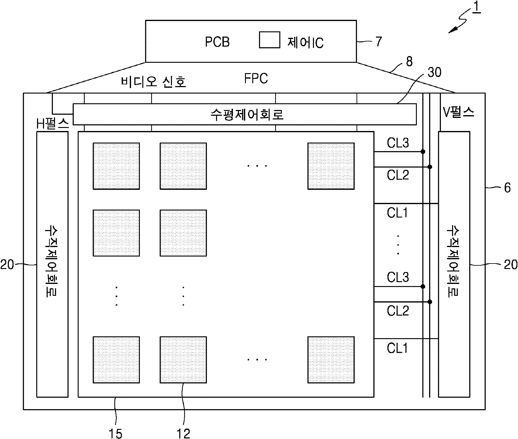
도 1은, 본 개시의 일 실시예에 따른 표시 장치(1)의 개략 구성을 나타내는 도면이다.
도 2는 본 개시의 일 실시예에 따른 수평 제어 회로(30)의 개략 구성을 나타내는 도면이다.
도 3은 본 개시의 일 실시예에 따른 화소 회로의 구조를 나타낸 도면이다.
도 4는 본 개시의 일 실시예에 따른 화소 회로 및 발광 제어부의 구성을 나타내는 회로도이다.
도 5는 본 개시의 일 실시예에 따른 발광 제어부와 복수의 화소 회로와의 접속 관계를 나타내는 회로도이다.
도 6은 본 개시의 일 실시예에 따른 표시 장치(1)의 구동 방법을 설명하기 위한 타이밍 차트이다.
도 7은 본 개시의 일 실시예에 따른 이동도(μ) 보정 방법을 설명하기 위한 타이밍 차트이다.
도 8은 본 개시의 일 실시예에 따른 타이밍 제어부의 구성을 나타내는 도면이다.
도 9는 본 개시의 다른 실시예에 따른 타이밍 제어부의 구성을 나타내는 도면이다.
도 10은 본 개시의 다른 실시예에 따른 화소 회로의 구성을 나타내는 회로도이다.
도 11은 도 10의 화소 회로를 이용하는 표시 장치의 구동 방법을 설명하기 위한 타이밍 차트이다.
도 12는 본 개시의 다른 실시예에 따른 이동도(μ) 보정 방법을 설명하기 위한 타이밍 차트이다.
도 13은 본 개시의 일 실시예에 따른 타이밍 제어부(1310a)의 구성을 나타내는 도면이다.
도 14는 본 개시의 다른 실시예에 따른 타이밍 제어부(1310b)의 구성을 나타내는 도면이다.
도 15는 본 개시의 또 다른 실시예에 따른 화소 회로를 나타낸 도면이다.
도 16은 본 개시의 또 다른 실시예에 따른 표시 장치(1)의 구동 방법을 설명하기 위한 타이밍 차트이다.
도 17은 본 개시의 또 다른 실시예에 따른 화소 회로(10c)의 구동 상태를 나타내는 도면이다.
도 18은 본 개시의 또 다른 실시예에 따른 화소 회로(10c)의 구동 상태를 나타내는 도면이다.
도 19은 본 개시의 또 다른 실시예에 따른 화소 회로(10c)의 구동 상태를 나타내는 도면이다.
도 20은 본 개시의 또 다른 실시예에 따른 화소 회로(10c)의 구동 상태를 나타내는 도면이다.
도 21은 본 개시의 또 다른 실시예에 따른 화소 회로(10c)의 구동 상태를 나타내는 도면이다.
도 22은 본 개시의 또 다른 실시예에 따른 화소 회로(10c)의 다른 구성을 나타내는 회로도이다.
도 23은 본 개시의 또 다른 실시예에 따른 화소 회로(10c)의 다른 구성을 나타내는 회로도이다.
도 24는 본 개시의 또 다른 실시예에 따른 실시예에 따른 화소 회로의 구조를 나타낸 도면이다.
도 25는 본 개시의 또 다른 실시예에 따른 표시 장치(1)의 구동 방법을 설명하기 위한 타이밍 차트이다.
도 26은 본 개시의 또 다른 실시예에 따른 화소 회로(10f)의 구동 상태를 나타내는 도면이다.
도 27은 본 개시의 또 다른 실시예에 따른 화소 회로(10f)의 구동 상태를 나타내는 도면이다.
도 28은 본 개시의 또 다른 실시예에 따른 화소 회로(10f)의 구동 상태를 나타내는 도면이다.
도 29은 본 개시의 또 다른 실시예에 따른 화소 회로(10f)의 구동 상태를 나타내는 도면이다.
도 30은 본 개시의 또 다른 실시예에 따른 화소 회로(10f)의 구동 상태를 나타내는 도면이다.
도 31은 본 개시의 또 다른 실시예에 따른 화소 회로(10f)의 구동 상태를 나타내는 도면이다.
도 32는 본 실시예에 따른 다른 화소 회로(10g)의 구성을 나타내는 회로도이다. FIG. 1 is a drawing showing a schematic configuration of a display device (1) according to one embodiment of the present disclosure.
FIG. 2 is a drawing showing a schematic configuration of a horizontal control circuit (30) according to one embodiment of the present disclosure.
FIG. 3 is a diagram showing the structure of a pixel circuit according to one embodiment of the present disclosure.
FIG. 4 is a circuit diagram showing the configuration of a pixel circuit and a light emission control unit according to one embodiment of the present disclosure.
FIG. 5 is a circuit diagram showing a connection relationship between a light-emitting control unit and a plurality of pixel circuits according to one embodiment of the present disclosure.
FIG. 6 is a timing chart for explaining a driving method of a display device (1) according to one embodiment of the present disclosure.
FIG. 7 is a timing chart for explaining a mobility (μ) compensation method according to one embodiment of the present disclosure.
FIG. 8 is a diagram showing the configuration of a timing control unit according to one embodiment of the present disclosure.
FIG. 9 is a diagram showing the configuration of a timing control unit according to another embodiment of the present disclosure.
FIG. 10 is a circuit diagram showing the configuration of a pixel circuit according to another embodiment of the present disclosure.
Fig. 11 is a timing chart for explaining a driving method of a display device using the pixel circuit of Fig. 10.
FIG. 12 is a timing chart for explaining a mobility (μ) compensation method according to another embodiment of the present disclosure.
FIG. 13 is a diagram showing the configuration of a timing control unit (1310a) according to one embodiment of the present disclosure.
FIG. 14 is a diagram showing the configuration of a timing control unit (1310b) according to another embodiment of the present disclosure.
FIG. 15 is a diagram illustrating a pixel circuit according to another embodiment of the present disclosure.
FIG. 16 is a timing chart for explaining a driving method of a display device (1) according to another embodiment of the present disclosure.
FIG. 17 is a drawing showing the driving state of a pixel circuit (10c) according to another embodiment of the present disclosure.
FIG. 18 is a drawing showing the driving state of a pixel circuit (10c) according to another embodiment of the present disclosure.
FIG. 19 is a drawing showing the driving state of a pixel circuit (10c) according to another embodiment of the present disclosure.
FIG. 20 is a drawing showing the driving state of a pixel circuit (10c) according to another embodiment of the present disclosure.
FIG. 21 is a drawing showing the driving state of a pixel circuit (10c) according to another embodiment of the present disclosure.
FIG. 22 is a circuit diagram showing another configuration of a pixel circuit (10c) according to another embodiment of the present disclosure.
FIG. 23 is a circuit diagram showing another configuration of a pixel circuit (10c) according to another embodiment of the present disclosure.
FIG. 24 is a diagram showing the structure of a pixel circuit according to an embodiment according to another embodiment of the present disclosure.
FIG. 25 is a timing chart for explaining a driving method of a display device (1) according to another embodiment of the present disclosure.
FIG. 26 is a drawing showing the driving state of a pixel circuit (10f) according to another embodiment of the present disclosure.
FIG. 27 is a drawing showing the driving state of a pixel circuit (10f) according to another embodiment of the present disclosure.
FIG. 28 is a drawing showing the driving state of a pixel circuit (10f) according to another embodiment of the present disclosure.
FIG. 29 is a drawing showing the driving state of a pixel circuit (10f) according to another embodiment of the present disclosure.
FIG. 30 is a drawing showing the driving state of a pixel circuit (10f) according to another embodiment of the present disclosure.
FIG. 31 is a drawing showing the driving state of a pixel circuit (10f) according to another embodiment of the present disclosure.
Fig. 32 is a circuit diagram showing the configuration of another pixel circuit (10g) according to the present embodiment.
발명의 실시를 위한 최선의 형태Best mode for carrying out the invention
본 개시의 일 실시예의 일 측면에 따르면, 복수의 화소 회로를 포함하고, 각각의 상기 복수의 화소 회로는, 발광 소자; 상기 발광 소자로의 전류 공급의 유무를 제어하는 PWM 제어부; 상기 발광 소자로 상기 전류를 공급하는 정전류 제어부를 포함하고, 제1 전원선과 제2 전원선 사이에 상기 정전류 제어부, 상기 PWM 제어부 및 상기 발광 소자를 직렬로 접속하여 상기 발광 소자로 상기 전류를 공급하고, 상기 제1 전원선과 상기 정전류 제어부 사이에, 정전류 설정 기간에 상기 발광 소자를 소등하기 위한 트랜지스터를 갖는 표시 장치가 제공된다.According to one aspect of one embodiment of the present disclosure, a display device is provided, which includes a plurality of pixel circuits, each of the plurality of pixel circuits including: a light-emitting element; a PWM control unit for controlling whether or not current is supplied to the light-emitting element; and a constant current control unit for supplying the current to the light-emitting element, wherein the constant current control unit, the PWM control unit and the light-emitting element are connected in series between a first power line and a second power line to supply the current to the light-emitting element, and wherein a transistor for turning off the light-emitting element during a constant current setting period is provided between the first power line and the constant current control unit.
발명의 실시를 위한 형태Form for carrying out the invention
본 명세서는 청구항의 권리범위를 명확히 하고, 본 발명이 속하는 기술분야에서 통상의 지식을 가진 자가 청구항에 기재된 실시예를 실시할 수 있도록, 실시예들의 원리를 설명하고 개시한다. 개시된 실시예들은 다양한 형태로 구현될 수 있다.This specification clarifies the scope of the claims and explains and discloses the principles of the embodiments so that a person having ordinary skill in the art to which the present invention pertains can practice the embodiments described in the claims. The disclosed embodiments can be implemented in various forms.
명세서 전체에 걸쳐 동일 참조 부호는 동일 구성요소를 지칭한다. 본 명세서가 실시예들의 모든 요소들을 설명하는 것은 아니며, 본 개시의 실시예들이 속하는 기술분야에서 일반적인 내용 또는 실시예들 간에 중복되는 내용은 생략한다. 명세서에서 사용되는 "모듈" 또는 "부"(unit)라는 용어는 소프트웨어, 하드웨어 또는 펌웨어 중 하나 또는 둘 이상의 조합으로 구현될 수 있으며, 실시예들에 따라 복수의 "모듈" 또는 "부"가 하나의 요소(element)로 구현되거나, 하나의 "모듈" 또는 "부"가 복수의 요소들을 포함하는 것도 가능하다. 이하 첨부된 도면들을 참고하여 본 개시의 실시예들의 작용 원리 및 다양한 실시예들에 대해 설명한다.Like reference numerals refer to like elements throughout the specification. This specification does not describe all elements of the embodiments, and general contents in the technical field to which the embodiments of the present disclosure belong or contents overlapping between the embodiments are omitted. The term "module" or "unit" used in the specification may be implemented by one or a combination of two or more of software, hardware, or firmware, and according to the embodiments, a plurality of "modules" or "units" may be implemented as a single element, or a single "module" or "unit" may include a plurality of elements. Hereinafter, the operating principles and various embodiments of the embodiments of the present disclosure will be described with reference to the accompanying drawings.
본 개시의 일 실시예에 따른 표시 장치는, 예컨대, 자발광형 액티브 매트릭스 디스플레이로서, 발광 소자 정전류 구동 및 펄스폭 변조에 의한 계조 표현을 수행하기 위해, 전원 사이에 발광 제어부, 정전류 제어부(정전류원), PWM 제어부, 및 발광 소자를 이 순서로 직렬로 접속한 것이다. A display device according to one embodiment of the present disclosure is, for example, a self-luminous active matrix display, in which a light-emitting control unit, a constant current control unit (constant current source), a PWM control unit, and a light-emitting element are connected in series in this order between a power supply to perform gradation expression by constant current driving of light-emitting elements and pulse width modulation.
여기서, 발광 소자, PWM 제어부, 및 정전류 제어부가 하나의 화소 회로를 구성한다. 또한, PWM 제어부 및 정전류 제어부는 각각 2개의 트랜지스터 및 하나의 커패시터로 구성된다. 즉, 본 개시의 일 실시예에 따르면, 하나의 화소 회로는 발광 소자, 4개의 트랜지스터 및 2개의 커패시터(4Tr2C)의 최소 소자수로 구성된다. 또한, 발광 제어부는 복수의 화소 회로에 접속된(스위칭) 트랜지스터를 포함할 수 있다.Here, a light-emitting element, a PWM control unit, and a constant current control unit constitute one pixel circuit. In addition, the PWM control unit and the constant current control unit are each composed of two transistors and one capacitor. That is, according to one embodiment of the present disclosure, one pixel circuit is composed of a minimum number of elements of a light-emitting element, four transistors, and two capacitors (4Tr2C). In addition, the light-emitting control unit may include a transistor connected (switching) to a plurality of pixel circuits.
또한, 본 개시의 실시예들에 따르면, 정전류 제어부가 정전류 설정을 수행하고, PWM 제어부가 발광 소자의 발광/비발광의 2개 상태 천이를 제어하고, 발광 제어부가 정전류 설정 시의 발광 소자의 비발광을 제어한다. 또한, 본 개시의 실시예들은, 화소 회로의 정전류 제어부, PWM 제어부, 및 발광 제어부 각각에 입력하는 제어 펄스와 전원 펄스에 의해, 정전류 설정 및 PWM 발광 제어를 가능하게 한다. 본 개시의 실시예들에 따르면, 정전류 PWM 구동에 의해, 발광 디바이스의 전류-전압(I-V) 특성 격차, 전류-광출력(I-L) 특성의 비선형성, 및 색온도의 전류 의존 비선형성을 보정하여 높은 발광 균일성을 실현할 수 있고, 또한 디지털 신호 입력에 의해 발광 기간을 제어하여 패널 발광 시간을 길게 하고, 고휘도화를 실현할 수 있다. In addition, according to embodiments of the present disclosure, the constant current control unit performs constant current setting, the PWM control unit controls the two-state transition of light emission/non-light emission of the light emitting element, and the light emission control unit controls non-light emission of the light emitting element at the time of constant current setting. In addition, embodiments of the present disclosure enable constant current setting and PWM light emission control by control pulses and power pulses input to each of the constant current control unit, the PWM control unit, and the light emission control unit of the pixel circuit. According to embodiments of the present disclosure, by constant current PWM driving, it is possible to correct the gap in current-voltage (I-V) characteristics of the light emitting device, the nonlinearity of current-light output (I-L) characteristics, and the current-dependent nonlinearity of color temperature, thereby realizing high light emission uniformity, and also to control the light emission period by digital signal input, thereby lengthening the panel light emission time and realizing high brightness.
본 개시의 실시예들은 75inch 8K 마이크로 LED TV를 구현하기 위해 이용될 수 있다. 마이크로 LED는 휘도 및 색도의 전류 의존성이 있어 고화질을 위해서는 정전류 및 시간 분할 구동으로 제어가 필요하다.Embodiments of the present disclosure can be used to implement a 75-inch 8K micro LED TV. Micro LEDs have current dependency in brightness and chromaticity, and thus require control through constant current and time division driving for high image quality.
한편, 8K 디스플레이에서는 기존 4K와 비교해 화소 면적이 1/4로 줄어든다. 따라서 75inch 8K 마이크로 LED TV를 실현하기 위해, 소자수가 적은 정전류 시간 분할 구동이 요구된다. 본 개시의 실시예들에 따르면, 최소 화소수 4.3T2C(4.3개의 트랜지스터와 2개의 커패시터)로 정전류형 디지털 PWM 구동을 실현해, 패널의 고화질화를 가능하게 할 수 있다. 또한, 이와 동시에 정전류원을 형성하는 트랜지스터 특성 편차를 보정하여, 높은 균일성(uniformity) 표시를 실현할 수 있다. Meanwhile, in the 8K display, the pixel area is reduced to 1/4 compared to the existing 4K. Therefore, in order to realize a 75-inch 8K micro LED TV, constant current time division driving with a small number of components is required. According to the embodiments of the present disclosure, constant current type digital PWM driving can be realized with a minimum pixel count of 4.3T2C (4.3 transistors and 2 capacitors), thereby enabling high picture quality of the panel. In addition, at the same time, by correcting the characteristic deviation of the transistor forming the constant current source, high uniformity display can be realized.
이하, 도면을 참조하여 본 개시의 일 실시예에 따른 표시 장치 및 표시 장치의 구동 방법에 대해 설명한다. Hereinafter, a display device and a method for driving the display device according to one embodiment of the present disclosure will be described with reference to the drawings.
우선, 본 개시의 일 실시예에 따른 표시 장치의 구성에 대해 설명한다. First, the configuration of a display device according to one embodiment of the present disclosure will be described.
도 1은, 본 개시의 일 실시예에 따른 표시 장치(1)의 개략 구성을 나타내는 도면이다. FIG. 1 is a drawing showing a schematic configuration of a display device (1) according to one embodiment of the present disclosure.
본 개시의 일 실시예에 따른 표시 장치(1)는, 자발광 발광소자를 포함하는 다양한 형태의 표시 장치에 대응될 수 있다. 표시 장치(1)는 예를 들면, LED(Light Emitting Diode) 디스플레이, 유기 EL(Electro Luminescence) 디스플레이 등에 대응될 수 있다. 표시 장치(1)는 패널(6), 제어부(7), 및 패널(6)과 PCB(7)을 접속하는 연성회로기판(FPC, Flexible Printed Circuit, 8)을 포함한다.A display device (1) according to one embodiment of the present disclosure may correspond to various types of display devices including a self-luminous light-emitting element. The display device (1) may correspond to, for example, an LED (Light Emitting Diode) display, an organic EL (Electro Luminescence) display, etc. The display device (1) includes a panel (6), a control unit (7), and a flexible printed circuit board (FPC, Flexible Printed Circuit, 8) connecting the panel (6) and the PCB (7).
또한, 패널(6)은 매트릭스 형태로 배치된 복수의 화소 회로(10)를 포함하는 화소 어레이(15), 수직 제어 회로(20), 및 수평 제어 회로(30) 등의 구동 회로를 포함한다. 또한, 패널(6)은 복수의 화소 회로(10) 각각에 배치되거나, 소정 개수의 화소 회로(10)의 그룹에 배치된 발광 제어부를 포함할 수 있다. 구동 회로를 구성하는 각 트랜지스터는, 예컨대, TFT(Thin Film Transistor:박막 트랜지스터)이다. In addition, the panel (6) includes a driving circuit such as a pixel array (15) including a plurality of pixel circuits (10) arranged in a matrix form, a vertical control circuit (20), and a horizontal control circuit (30). In addition, the panel (6) may include a light emitting control unit arranged in each of the plurality of pixel circuits (10) or arranged in a group of a predetermined number of pixel circuits (10). Each transistor constituting the driving circuit is, for example, a TFT (Thin Film Transistor).
패널(6)의 각각의 화소 회로(10)는 하나의 화소를 구성하는 서브 화소에 대응될 수 있다. 하나의 화소는 복수의 서브 화소로 정의된다. 하나의 화소에 포함되는 서브 화소들은 각각 소정의 색 성분에 대응되고, 하나의 화소는 복수의 색 성분에 대응하는 서브 화소들을 포함한다. 예를 들면, 하나의 화소가 서브 화소 R(빨강), G(초록), 및 B(파랑)에 각각 대응하는 3개의 화소 회로(10)로 정의될 수 있다. 다른 예로서, 하나의 화소가 하나의 R 서브 화소, 2개의 G 서브 화소, 및 1개의 B 서브 화소로 이루어질 수 있다. 하나의 화소에 포함되는 서브 화소의 색 성분 조합은 실시예에 따라 다양하게 결정될 수 있다. 또한, 일 실시예에 따르면, 각 열에 다른 색에 대응하는 화소 회로(10)가 배치될 수 있다. 예컨대, 1열째로부터 차례로, R에 대응하는 화소 회로(10)의 열, G에 대응하는 화소 회로(10)의 열, B에 대응하는 화소 회로(10)의 열과 같이 다른 색에 대응하는 화소 회로(10)의 열이 반복적으로 나열될 수 있다.Each pixel circuit (10) of the panel (6) may correspond to a sub-pixel constituting one pixel. One pixel is defined by a plurality of sub-pixels. The sub-pixels included in one pixel each correspond to a predetermined color component, and one pixel includes sub-pixels corresponding to a plurality of color components. For example, one pixel may be defined by three pixel circuits (10) corresponding to sub-pixels R (red), G (green), and B (blue), respectively. As another example, one pixel may be composed of one R sub-pixel, two G sub-pixels, and one B sub-pixel. The color component combinations of the sub-pixels included in one pixel may be determined in various ways depending on the embodiment. In addition, according to one embodiment, pixel circuits (10) corresponding to different colors may be arranged in each column. For example, columns of pixel circuits (10) corresponding to different colors may be repeatedly listed, such as a column of pixel circuits (10) corresponding to R, a column of pixel circuits (10) corresponding to G, and a column of pixel circuits (10) corresponding to B, in that order from the first column.
수직 제어 회로(20)는 적어도 하나의 게이트 라인(CL1, CL2, CL3)을 통해 각 화소 회로(10)로 적어도 하나의 종류의 제어 신호를 출력한다. 예를 들면, 수직 제어 회로(20)는 제1 게이트 라인(CL1)을 선택하여 PWM 제어를 위한 신호를 화소 회로(10)의 행마다 공급한다. 수직 제어 회로(20)는 각 행에 대응하는 복수의 스테이지 회로를 포함하고, 복수의 스테이지 회로는 각 행에 대응하는 수직 제어 신호를 순차적으로 생성하여 출력할 수 있다. The vertical control circuit (20) outputs at least one type of control signal to each pixel circuit (10) through at least one gate line (CL1, CL2, CL3). For example, the vertical control circuit (20) selects the first gate line (CL1) and supplies a signal for PWM control to each row of the pixel circuit (10). The vertical control circuit (20) includes a plurality of stage circuits corresponding to each row, and the plurality of stage circuits can sequentially generate and output vertical control signals corresponding to each row.
수평 제어 회로(30)는 영상 데이터의 각 화소 값에 대응하는 데이터 신호를 생성하여 데이터 라인(DL1)을 통해 각 열의 화소 회로(10)로 출력한다. 수평 제어 회로(30)는 PCB(7)로부터 출력되어 FPC(8)를 통해 전달된 디지털 신호(영상 신호) 또는 아날로그 신호를 선택하여 각 열에 대응하는 데이터 라인(DL1)에 공급한다. 수평 제어 회로(30)는 PCB(7)로부터 각 열에 대응하는 데이터 신호를 순차적으로 입력 받고, 데이터 신호에 대응하는 열로 데이터 신호를 출력하기 위해, 셀렉터 제어, 디멀티플렉서 제어 등을 수행한다.The horizontal control circuit (30) generates a data signal corresponding to each pixel value of image data and outputs it to the pixel circuit (10) of each column through the data line (DL1). The horizontal control circuit (30) selects a digital signal (image signal) or an analog signal output from the PCB (7) and transmitted through the FPC (8) and supplies it to the data line (DL1) corresponding to each column. The horizontal control circuit (30) sequentially receives a data signal corresponding to each column from the PCB (7) and performs selector control, demultiplexer control, etc. to output the data signal to the column corresponding to the data signal.
제어부(7)는 수평 제어 펄스(H펄스) 및 수직 제어 펄스(V펄스)를 생성하여 각각 수평 제어 회로(30) 및 수직 제어 회로(20)로 출력한다. 제어부(7)는 수평 제어 펄스 및 수직 제어 펄스를 이용하여 수평 제어 회로(30)와 수직 제어 회로(20)에서 각 화소 회로(10)로 데이터 신호 및 수직 제어 신호가 출력되는 타이밍을 제어할 수 있다. 또한, 제어부(7)는 데이터 신호를 다른 프로세서 또는 외부 장치로부터 수신하여, 수평 제어 회로(30)로 출력할 수 있다. 제어부(7)는 제어 IC를 탑재한 인쇄회로기판(PCB, Printed Circuit Board)의 형태로 구현될 수 있다.The control unit (7) generates horizontal control pulses (H pulses) and vertical control pulses (V pulses) and outputs them to the horizontal control circuit (30) and the vertical control circuit (20), respectively. The control unit (7) can control the timing at which data signals and vertical control signals are output from the horizontal control circuit (30) and the vertical control circuit (20) to each pixel circuit (10) using the horizontal control pulses and the vertical control pulses. In addition, the control unit (7) can receive data signals from another processor or an external device and output them to the horizontal control circuit (30). The control unit (7) can be implemented in the form of a printed circuit board (PCB) equipped with a control IC.
도 2는 본 개시의 일 실시예에 따른 수평 제어 회로(30)의 개략 구성을 나타내는 도면이다. FIG. 2 is a drawing showing a schematic configuration of a horizontal control circuit (30) according to one embodiment of the present disclosure.
수평 제어 회로(30)는 비디오 샘플링 회로(36) 및 정전류 제어 신호 스위칭 회로(37)를 포함한다. 비디오 샘플링 회로(36)는 입력 영상 신호에 대응하는 데이터 신호를 정전류 제어 신호 스위칭 회로(37)로 전달한다. 비디오 샘플링 회로(36)는 화소 어레이(12)의 복수의 열에 각각 대응하는 데이터 신호를 순차적으로 출력할 수 있다. 이를 위해, 비디오 샘플링 회로(36)는 데이터 신호를 화소 어레이의 복수의 열로 순차적으로 출력하기 위한 셀렉터 제어 또는 디멀티플렉서 제어를 수행할 수 있다. 비디오 샘플링 회로(36)는 다양한 구조의 셀렉터 회로 또는 디멀티플렉서 회로를 포함할 수 있다. 일 실시예에 따르면, 비디오 샘플링 회로(36)는 화소에 포함되는 서브 화소들의 색 성분 각각에 대응하는 샘플링 회로를 별도로 구비할 수 있다. 예를 들면, 화소가 R, G, B의 세가지 서브 화소를 포함하는 경우, 비디오 샘플링 회로(36)는 R 샘플링 회로, G 샘플링 회로, 및 B 샘플링 회로를 포함할 수 있다.The horizontal control circuit (30) includes a video sampling circuit (36) and a constant current control signal switching circuit (37). The video sampling circuit (36) transmits a data signal corresponding to an input image signal to the constant current control signal switching circuit (37). The video sampling circuit (36) can sequentially output data signals corresponding to each of a plurality of columns of the pixel array (12). To this end, the video sampling circuit (36) can perform selector control or demultiplexer control to sequentially output the data signals to the plurality of columns of the pixel array. The video sampling circuit (36) can include selector circuits or demultiplexer circuits of various structures. According to one embodiment, the video sampling circuit (36) can separately have a sampling circuit corresponding to each color component of sub-pixels included in the pixel. For example, when the pixel includes three sub-pixels of R, G, and B, the video sampling circuit (36) can include an R sampling circuit, a G sampling circuit, and a B sampling circuit.
정전류 제어 신호 스위칭 회로(37)는 비디오 샘플링 회로(36)에서 출력된 데이터 신호를 수신하여, 화소 어레이(12)의 각 열에 대응하는 각각의 데이터 라인(DL1)으로 출력한다. 정전류 제어 신호 스위칭 회로(37)는 비디오 샘플링 회로(36)로부터 입력된 데이터 신호에 대응하는 열의 데이터 라인(DL1)을 선택하여 데이터 신호를 선택된 데이터 라인(DL1)으로 출력한다. 이와 같은 스위칭 제어에 의해, 정전류 제어 신호 스위칭 회로(37)는 서브 프레임 기간에 각 화소 회로(10)에 데이터 신호를 공급하고, 정전류 설정 기간에 각 화소 회로(10)에 오프셋 전압(기준 전압)(Vofs) 또는 참조 전압(Vref)을 갖는 아날로그 신호를 공급한다. 정전류 제어 신호 스위칭 회로(37)는 데이터 라인(DL1)을 선택하는 제1 선택 회로(TRsel1), 오프셋 전압(Vofs)을 인가하는 제2 선택 회로(TRsel2), 참조 전압(Vref)을 인가하는 제3 선택 회로(TRsel3)를 포함할 수 있다. 제1 선택 회로(TRsel1)는 각 데이터 라인(DL1)에 대응하는 스위칭 트랜지스터를 포함하고, SEL Video 제어 신호에 의해 각 스위칭 트랜지스터가 온/오프됨에 의해 데이터 라인(DL1)이 선택될 수 있다. 제2 선택 회로(TRsel2)는 제1 단자가 오프셋 전압(Vofs)의 전압원에 연결되고, 제2 단자가 각 데이터 라인(DL1)에 연결되고, 게이트 단자가 SEL ofs 신호 선에 연결된 복수의 스위칭 트랜지스터를 포함한다. 정전류 제어 신호 스위칭 회로(37)는 SEL ofs 신호에 의해 각 데이터 라인(DL1)에 오프셋 전압(Vofs)의 인가를 제어할 수 있다. 제3 선택 회로(TRsel3)는 제1 단자가 참조 전압(Vref) 전압원에 연결되고, 제2 단자가 각 데이터 라인(DL1)에 연결되고, 게이트 단자가 SEL ref 신호 선에 연결된 복수의 스위칭 트랜지스터를 포함한다. 참조 전압(Vref)은 각 색 성분에 대응하는 복수의 참조 전압 Vref R, Vref G, Vref B를 포함할 수 있다. 데이터 라인(DL1)은 R(red)에 대응하는 R 데이터 라인(DL1R), G(green)에 대응하는 G 데이터 라인(DL1G), B(blue)에 대응하는 B 데이터 라인(DL1B)을 포함할 수 있다. 각 데이터 라인(DL1)은 해당 데이터 라인(DL1)의 색 성분에 대응하는 참조 전압(Vref R, Vref G, 또는 Vref B)의 전압원에 연결될 수 있다. 정전류 제어 신호 스위칭 회로(37)는 SEL ref 신호에 의해 각 데이터 라인(DL1)에 참조 전압(Vref R, Vref G, Vref B)의 인가를 제어할 수 있다. 서브 프레임 기간, 정전류 설정 기간, 오프셋 전압(Vofs), 참조 전압(Vref)에 대해서는 후술한다. The constant current control signal switching circuit (37) receives the data signal output from the video sampling circuit (36) and outputs it to each data line (DL1) corresponding to each column of the pixel array (12). The constant current control signal switching circuit (37) selects the data line (DL1) of the column corresponding to the data signal input from the video sampling circuit (36) and outputs the data signal to the selected data line (DL1). By this switching control, the constant current control signal switching circuit (37) supplies a data signal to each pixel circuit (10) in the sub-frame period and supplies an analog signal having an offset voltage (reference voltage) (Vofs) or a reference voltage (Vref) to each pixel circuit (10) in the constant current setting period. The constant current control signal switching circuit (37) may include a first selection circuit (TRsel1) for selecting the data line (DL1), a second selection circuit (TRsel2) for applying the offset voltage (Vofs), and a third selection circuit (TRsel3) for applying the reference voltage (Vref). The first selection circuit (TRsel1) includes a switching transistor corresponding to each data line (DL1), and the data line (DL1) can be selected by turning each switching transistor on/off by the SEL Video control signal. The second selection circuit (TRsel2) includes a plurality of switching transistors, each of which has a first terminal connected to a voltage source of an offset voltage (Vofs), a second terminal connected to each data line (DL1), and a gate terminal connected to the SEL ofs signal line. The constant current control signal switching circuit (37) can control the application of the offset voltage (Vofs) to each data line (DL1) by the SEL ofs signal. The third selection circuit (TRsel3) includes a plurality of switching transistors, each of which has a first terminal connected to a voltage source of a reference voltage (Vref), a second terminal connected to each data line (DL1), and a gate terminal connected to the SEL ref signal line. The reference voltage (Vref) can include a plurality of reference voltages Vref R, Vref G, and Vref B corresponding to each color component. The data line (DL1) may include an R data line (DL1R) corresponding to R (red), a G data line (DL1G) corresponding to G (green), and a B data line (DL1B) corresponding to B (blue). Each data line (DL1) may be connected to a voltage source of a reference voltage (Vref R, Vref G, or Vref B) corresponding to a color component of the corresponding data line (DL1). The constant current control signal switching circuit (37) may control the application of the reference voltage (Vref R, Vref G, Vref B) to each data line (DL1) by the SEL ref signal. The sub-frame period, the constant current setting period, the offset voltage (Vofs), and the reference voltage (Vref) will be described later.
도 3은 본 개시의 일 실시예에 따른 화소 회로의 구조를 나타낸 도면이다. 도 3의 화소 회로(10a)는 화소 어레이(12)의 m행 n열의 화소에 대응된다(m, n은 자연수).Fig. 3 is a diagram showing the structure of a pixel circuit according to one embodiment of the present disclosure. The pixel circuit (10a) of Fig. 3 corresponds to a pixel in row m and column n of a pixel array (12) (m and n are natural numbers).
화소 회로(10a)는 발광 소자(EL1), 제1 전류 제어부(310) 및 제2 전류 제어부(320)를 구비한다. 또한, 제1 전류 제어부(310)는 제3 트랜지스터(Tr3), 제4 트랜지스터(Tr4) 및 제2 커패시터(C2)를 포함하고, 제2 전류 제어부(320)는 제1 트랜지스터(Tr1), 제2 트랜지스터(Tr2) 및 제1 커패시터(C1)를 포함한다. 제1 전류 제어부(310) 및 제2 전류 제어부(320) 중 하나는 PWM 제어부에 대응하고, 다른 하나는 정전류 제어부에 대응한다. 본 개시의 실시예에 따라 제1 전원, PWM 제어부, 정전류 제어부, 발광 소자, 및 제2 전원의 순서로 직렬 연결되거나, 제1 전원, 정전류 제어부, PWM 제어부, 발광 소자, 및 제2 전원의 순서로 직렬 연결될 수 있다. 제1 전류 제어부(310) 및 제2 전류 제어부(320) 중 PWM 제어부에 대응하는 회로로 PWM 제어를 위한 제어 신호 및가 인가되고, 정전류 제어부에 대응하는 회로로 정전류 제어를 위한 제어 신호가 인가될 수 있다.The pixel circuit (10a) includes a light-emitting element (EL1), a first current control unit (310), and a second current control unit (320). In addition, the first current control unit (310) includes a third transistor (Tr3), a fourth transistor (Tr4), and a second capacitor (C2), and the second current control unit (320) includes a first transistor (Tr1), a second transistor (Tr2), and a first capacitor (C1). One of the first current control unit (310) and the second current control unit (320) corresponds to a PWM control unit, and the other corresponds to a constant current control unit. According to an embodiment of the present disclosure, the first power source, the PWM control unit, the constant current control unit, the light-emitting element, and the second power source may be connected in series in that order, or the first power source, the constant current control unit, the PWM control unit, the light-emitting element, and the second power source may be connected in series in that order. A control signal for PWM control may be applied to a circuit corresponding to the PWM control unit among the first current control unit (310) and the second current control unit (320), and a control signal for constant current control may be applied to a circuit corresponding to the constant current control unit.
발광 소자(EL1)는 발광 다이오드(EL1)로서, 일반적인 용량 특성(용량 성분 C3)을 가지고 있고, 용량 디바이스로도 이용한다. 화소 회로(10a)는 발광 다이오드(EL1)가 용량 성분을 가지고 있지 않을 때는, 발광 다이오드(EL1)와는 별도로, TFT 디바이스의 상응하는 커패시터 C3를 구비하는 것이 바람직하다. 또한, 발광 다이오드(EL1)의 캐소드(cathode)은 제2 전원선(Vss)에 전기적으로 접속되고, 발광 다이오드(EL1)의 애노드(anode)는 제1 트랜지스터(Tr1)의 소스 단자에 전기적으로 접속된다. The light-emitting element (EL1) is a light-emitting diode (EL1), has general capacitance characteristics (capacitance component C3), and is also used as a capacitance device. When the light-emitting diode (EL1) does not have a capacitance component, it is preferable that the pixel circuit (10a) has a corresponding capacitor C3 of a TFT device separately from the light-emitting diode (EL1). In addition, the cathode of the light-emitting diode (EL1) is electrically connected to a second power line (Vss), and the anode of the light-emitting diode (EL1) is electrically connected to a source terminal of the first transistor (Tr1).
제1 트랜지스터(Tr1)는 게이트 단자는 제2 트랜지스터(Tr2)의 소스 단자 및 제1 커패시터(C1)의 일방의 단자에 전기적으로 접속되고, 소스 단자는 발광 다이오드(EL1)의 애노드 및 제1 커패시터(C1)의 다른 일방의 단자에 전기적으로 접속되며, 드레인 단자는 제3 트랜지스터(Tr3)의 소스 단자 및 제2 커패시터(C2)의 다른 일방의 단자에 전기적으로 접속된다.A first transistor (Tr1) has a gate terminal electrically connected to a source terminal of a second transistor (Tr2) and one terminal of a first capacitor (C1), a source terminal electrically connected to an anode of a light-emitting diode (EL1) and the other terminal of the first capacitor (C1), and a drain terminal electrically connected to a source terminal of a third transistor (Tr3) and the other terminal of the second capacitor (C2).
제2 트랜지스터(Tr2)는 데이터 라인(DL1)로부터 데이터 신호를 수신하는 타이밍을 제어하는 트랜지스터이고, 그 게이트 단자는 제1 게이트 라인(CL1)에 전기적으로 접속되고, 드레인 단자는 데이터 라인(DL1)에 전기적으로 접속되고, 소스 단자는 제1 트랜지스터(Tr1)의 게이트 단자 및 제1 커패시터(C1)의 일방의 단자에 전기적으로 접속된다. The second transistor (Tr2) is a transistor that controls the timing of receiving a data signal from the data line (DL1), and its gate terminal is electrically connected to the first gate line (CL1), its drain terminal is electrically connected to the data line (DL1), and its source terminal is electrically connected to the gate terminal of the first transistor (Tr1) and one terminal of the first capacitor (C1).
제1 커패시터(C1)는 제1 트랜지스터(Tr1)의 게이트 전압(Vg)을 홀딩하는 소자이고, 그 일방의 단자는 제1 트랜지스터(Tr1)의 게이트 단자 및 제2 트랜지스터(Tr2)의 소스 단자에 전기적으로 접속된다. 또한, 제1 커패시터(C1)의 다른 일방의 단자는 제1 트랜지스터(Tr1)의 소스 단자에 전기적으로 접속될 수도 있고, 예컨대, 0V(접지) 등의 고정 전원에 전기적으로 접속될 수도 있다. The first capacitor (C1) is an element that holds the gate voltage (Vg) of the first transistor (Tr1), and one terminal of the first capacitor (C1) is electrically connected to the gate terminal of the first transistor (Tr1) and the source terminal of the second transistor (Tr2). In addition, the other terminal of the first capacitor (C1) may be electrically connected to the source terminal of the first transistor (Tr1) or may be electrically connected to a fixed power source such as 0 V (ground).
제3 트랜지스터(Tr3)는 게이트 단자는 제4 트랜지스터(Tr4)의 소스 단자 및 제2 커패시터(C2)의 일방의 단자에 전기적으로 접속되고, 소스 단자는 제1 트랜지스터(Tr1)의 드레인 단자에 전기적으로 접속되고, 드레인 단자는 제1 전원선(Vdd)에 전기적으로 접속된다. 제3 트랜지스터(Tr3)의 드레인 단자는 제1 전원선(Vdd)에 직접 접속되거나, 적어도 하나의 스위칭 트랜지스터를 통해 접속될 수 있다.A third transistor (Tr3) has a gate terminal electrically connected to a source terminal of a fourth transistor (Tr4) and one terminal of a second capacitor (C2), a source terminal electrically connected to a drain terminal of the first transistor (Tr1), and a drain terminal electrically connected to a first power line (Vdd). The drain terminal of the third transistor (Tr3) may be directly connected to the first power line (Vdd) or may be connected through at least one switching transistor.
제4 트랜지스터(Tr4)는 데이터 라인(DL1)으로부터의 데이터 신호를 제3 트랜지스터(Tr3)로 전달하는 타이밍을 제어하는 트랜지스터이고, 그 게이트 단자는 제2 게이트 라인(CL2)에 전기적으로 접속되고, 드레인 단자는 데이터 라인(DL1)에 전기적으로 접속되며, 소스 단자는 제3 트랜지스터(Tr3)의 게이트 단자 및 제2 커패시터(C2)의 일방의 단자에 전기적으로 접속된다. The fourth transistor (Tr4) is a transistor that controls the timing of transmitting a data signal from the data line (DL1) to the third transistor (Tr3), and its gate terminal is electrically connected to the second gate line (CL2), its drain terminal is electrically connected to the data line (DL1), and its source terminal is electrically connected to the gate terminal of the third transistor (Tr3) and one terminal of the second capacitor (C2).
제2 커패시터(C2)는 제3 트랜지스터(Tr3)의 게이트 전압(Vg)을 홀딩하는 소자이고, 일방의 단자는 제3 트랜지스터(Tr3)의 게이트 단자 및 제4 트랜지스터(Tr4)의 소스 단자에 전기적으로 접속되며, 다른 일방의 단자는 제3 트랜지스터(Tr3)의 소스 단자에 전기적으로 접속되거나, 0V(접지) 등의 고정 전원에 전기적으로 접속될 수도 있다. The second capacitor (C2) is an element that holds the gate voltage (Vg) of the third transistor (Tr3), and one terminal is electrically connected to the gate terminal of the third transistor (Tr3) and the source terminal of the fourth transistor (Tr4), and the other terminal is electrically connected to the source terminal of the third transistor (Tr3) or may be electrically connected to a fixed power source such as 0 V (ground).
화소 회로(10a)는 제1 전원선(Vdd)과 정전류 제어부 사이에 정전류 설정 기간에 발광 소자(EL1)를 소등하기 위한 트랜지스터를 포함한다. 본 개시의 실시예들에 따른 표시 장치(1)는 정전류 제어부에 소스 팔로워형 트랜지스터를 포함한다. 표시 장치(1)는 소스 팔로워형 트랜지스터의 Vgs를 초기화하고, 트랜지스터의 Vgs를 정전류 제어부의 소스 팔로워형 트랜지스터의 문턱값 전압 Vgs로 설정하여 Vth 보상을 하기 위한 정전류 설정 기간을 포함한다. 정전류 설정 기간은 PWM 제어에 의한 발광 기간 전에 수행된다. 화소 회로(10a)는 정전류 설정 기간 동안 발광 소자(EL1)를 소등하기 위한 트랜지스터를 포함한다. 이러한 소등하기 위한 트랜지스터는 실시예에 따라, 도 3의 Tr1 내지 Tr4 이외의 별도의 트랜지스터로 구비되거나, PWM 제어부의 트랜지스터가 소등하기 위한 트랜지스터로 이용될 수 있다. The pixel circuit (10a) includes a transistor for turning off the light-emitting element (EL1) during a constant current setting period between the first power line (Vdd) and the constant current control unit. The display device (1) according to embodiments of the present disclosure includes a source follower transistor in the constant current control unit. The display device (1) includes a constant current setting period for initializing Vgs of the source follower transistor and setting Vgs of the transistor to a threshold voltage Vgs of the source follower transistor of the constant current control unit to perform Vth compensation. The constant current setting period is performed before the light-emitting period by PWM control. The pixel circuit (10a) includes a transistor for turning off the light-emitting element (EL1) during the constant current setting period. Depending on the embodiment, the transistor for turning off may be provided as a separate transistor other than Tr1 to Tr4 of FIG. 3, or the transistor of the PWM control unit may be used as a transistor for turning off the light.
이하 본 개시의 다양한 실시예에 따른 다양한 구조의 화소 회로 및 그 구동 방법에 대해 설명한다.Below, pixel circuits of various structures and their driving methods according to various embodiments of the present disclosure are described.
도 4는 본 개시의 일 실시예에 따른 화소 회로 및 발광 제어부의 구성을 나타내는 회로도이다. FIG. 4 is a circuit diagram showing the configuration of a pixel circuit and a light emission control unit according to one embodiment of the present disclosure.
본 개시의 일 실시예에 따르면, 화소 회로(10a)는 발광 소자(EL1), PWM 제어부(310a) 및 정전류 제어부(320a)를 구비한다. 또한, PWM 제어부(310a)는 제4-1 트랜지스터(Tr401), 제4-2 트랜지스터(Tr402) 및 제4-1 커패시터(C401)를 포함한다. 정전류 제어부(320a)는 제4-3 트랜지스터(Tr403), 제4-4 트랜지스터(Tr404) 및 제4-2 커패시터(C402)를 포함한다. 발광 제어부(410a)는 제4-5 트랜지스터(Tr405)를 포함한다. According to one embodiment of the present disclosure, a pixel circuit (10a) includes a light-emitting element (EL1), a PWM control unit (310a), and a constant current control unit (320a). In addition, the PWM control unit (310a) includes a 4-1st transistor (Tr401), a 4-2nd transistor (Tr402), and a 4-1st capacitor (C401). The constant current control unit (320a) includes a 4-3rd transistor (Tr403), a 4-4th transistor (Tr404), and a 4-2nd capacitor (C402). The light-emitting control unit (410a) includes a 4-5th transistor (Tr405).
발광 소자(EL1)는, 여기서는 발광 다이오드(EL1)로서, 일반적인 용량 특성(용량 성분 C3)을 가지고 있고, 커패시터로도 이용한다. 화소 회로(10a)는 발광 다이오드(EL1)가 용량 성분을 가지고 있지 않을 때는, 발광 다이오드(EL1)와는 별도로, 제3 커패시터(C3)를 포함할 수 있다. 커패시터(C3)는 발광 다이오드(EL1) 양단에 발광 다이오드(EL1)와 병렬로 연결될 수 있다. 또한, 발광 다이오드(EL1)의 캐소드는 제2 전원선(Vss)에 전기적으로 접속되고, 발광 다이오드(EL1)의 애노드는 제4-1 트랜지스터(Tr401)의 소스 단자에 전기적으로 접속된다. The light-emitting element (EL1), here a light-emitting diode (EL1), has general capacitance characteristics (capacitance component C3) and is also used as a capacitor. When the light-emitting diode (EL1) does not have a capacitance component, the pixel circuit (10a) may include a third capacitor (C3) separately from the light-emitting diode (EL1). The capacitor (C3) may be connected in parallel with the light-emitting diode (EL1) at both ends of the light-emitting diode (EL1). In addition, the cathode of the light-emitting diode (EL1) is electrically connected to the second power line (Vss), and the anode of the light-emitting diode (EL1) is electrically connected to the source terminal of the 4-1 transistor (Tr401).
제4-1 트랜지스터(Tr401)는 발광 다이오드(EL1)로의 전류 공급의 유무를 스위칭하는 트랜지스터이고, 그 게이트 단자는 제4-2 트랜지스터(Tr402)의 소스 단자 및 제4-1 커패시터(C401)의 일방의 단자에 전기적으로 접속되고, 소스 단자는 발광 다이오드(EL1)의 애노드 및 제4-1 커패시터(C401)의 다른 일방의 단자에 전기적으로 접속되며, 드레인 단자는 제4-3 트랜지스터(Tr403)의 소스 단자 및 제4-2 커패시터(C402)의 다른 일방의 단자에 전기적으로 접속된다. The 4-1 transistor (Tr401) is a transistor that switches whether current is supplied to the light-emitting diode (EL1), and its gate terminal is electrically connected to the source terminal of the 4-2 transistor (Tr402) and one terminal of the 4-1 capacitor (C401), the source terminal is electrically connected to the anode of the light-emitting diode (EL1) and the other terminal of the 4-1 capacitor (C401), and the drain terminal is electrically connected to the source terminal of the 4-3 transistor (Tr403) and the other terminal of the 4-2 capacitor (C402).
제4-2 트랜지스터(Tr402)는 데이터 라인(DL1)로부터 PWM 제어에 따른 신호를 수신하는 타이밍을 제어하는 트랜지스터이다. 제4-2 트랜지스터(Tr402)는 그 게이트 단자가 제4-1 게이트 라인(CL401)에 전기적으로 접속되고, 드레인 단자가 데이터 라인(DL1)에 전기적으로 접속되고, 소스 단자가 제4-1 트랜지스터(Tr401)의 게이트 단자 및 제4-1 커패시터(C401)의 일방의 단자에 전기적으로 접속된다. The 4-2 transistor (Tr402) is a transistor that controls the timing of receiving a signal according to PWM control from the data line (DL1). The 4-2 transistor (Tr402) has a gate terminal electrically connected to the 4-1 gate line (CL401), a drain terminal electrically connected to the data line (DL1), and a source terminal electrically connected to the gate terminal of the 4-1 transistor (Tr401) and one terminal of the 4-1 capacitor (C401).
제4-1 커패시터(C401)는 제4-1 트랜지스터(Tr401)의 게이트 전압(Vg)을 홀딩하는, 즉, PWM 제어부(310a)의 데이터를 홀딩하는 소자이고, 그 일방의 단자는 제4-1 트랜지스터(Tr401)의 게이트 단자 및 제4-2 트랜지스터(Tr402)의 소스 단자에 전기적으로 접속된다. 또한, 제4-1 커패시터(C401)의 다른 일방의 단자는 제4-1 트랜지스터(Tr401)의 소스 단자에 전기적으로 접속되거나, 접지 등의 고정 전원에 전기적으로 접속될 수도 있다. The 4-1 capacitor (C401) is an element that holds the gate voltage (Vg) of the 4-1 transistor (Tr401), i.e., holds the data of the PWM control unit (310a), and one terminal of the capacitor is electrically connected to the gate terminal of the 4-1 transistor (Tr401) and the source terminal of the 4-2 transistor (Tr402). In addition, the other terminal of the 4-1 capacitor (C401) may be electrically connected to the source terminal of the 4-1 transistor (Tr401) or may be electrically connected to a fixed power source such as ground.
또한, 제4-3 트랜지스터(Tr403)는 발광 다이오드(EL1)로의 공급 전류를 제어하는 트랜지스터이고, 그 게이트 단자는 제4-4 트랜지스터(Tr404)의 소스 단자 및 제4-2 커패시터(C402)의 일방의 단자에 전기적으로 접속되고, 소스 단자는 제4-1 트랜지스터(Tr401)의 드레인 단자 및 제4-2 커패시터(C402)의 다른 일방의 단자에 전기적으로 접속되고, 드레인 단자는 제4-5 트랜지스터(Tr405)의 소스 단자에 전기적으로 접속된다. In addition, the 4-3 transistor (Tr403) is a transistor that controls the supply current to the light-emitting diode (EL1), and its gate terminal is electrically connected to the source terminal of the 4-4 transistor (Tr404) and one terminal of the 4-2 capacitor (C402), the source terminal is electrically connected to the drain terminal of the 4-1 transistor (Tr401) and the other terminal of the 4-2 capacitor (C402), and the drain terminal is electrically connected to the source terminal of the 4-5 transistor (Tr405).
제4-4 트랜지스터(Tr404)는 데이터 라인(DL1)으로부터 정전류 설정에 따른 신호를 수신하는 타이밍을 제어하는 트랜지스터이고, 그 게이트 단자는 제4-2 게이트 라인(CL402)에 전기적으로 접속되고, 드레인 단자는 데이터 라인(DL401)에 전기적으로 접속되며, 소스 단자는 제4-3 트랜지스터(Tr403)의 게이트 단자 및 제4-2 커패시터(C402)의 일방의 단자에 전기적으로 접속된다. The 4-4 transistor (Tr404) is a transistor that controls the timing of receiving a signal according to a constant current setting from the data line (DL1), and its gate terminal is electrically connected to the 4-2 gate line (CL402), its drain terminal is electrically connected to the data line (DL401), and its source terminal is electrically connected to the gate terminal of the 4-3 transistor (Tr403) and one terminal of the 4-2 capacitor (C402).
제4-2 커패시터(C402)는 제4-3 트랜지스터(Tr403)의 게이트 전압(Vg)을 홀딩하는 소자이고, 일방의 단자는 제4-3 트랜지스터(Tr403)의 게이트 단자 및 제4-4 트랜지스터(Tr404)의 소스 단자에 전기적으로 접속되며, 다른 일방의 단자는 제4-3 트랜지스터(Tr403)의 소스 단자 및 제4-1 트랜지스터(Tr401)의 드레인 단자에 전기적으로 접속된다. The 4-2 capacitor (C402) is an element that holds the gate voltage (Vg) of the 4-3 transistor (Tr403), and one terminal is electrically connected to the gate terminal of the 4-3 transistor (Tr403) and the source terminal of the 4-4 transistor (Tr404), and the other terminal is electrically connected to the source terminal of the 4-3 transistor (Tr403) and the drain terminal of the 4-1 transistor (Tr401).
여기서는, 정전류 제어부(320a)는 게이트 접지형의 소스 팔로워형 회로이고, 제4-3 트랜지스터(Tr403)의 커플링 제어가 불필요하다는 점에서, 화소 회로(10a) 및 발광 제어부(410a)로 제어 신호를 전달하는 게이트 라인(CL401, CL402, CL403)의 수를 3개까지 줄일 수 있다. 또한, 제4-3 트랜지스터(Tr403)의 게이트에서 정전류 제어를 수행할 수 있으므로, 제2 전원선(Vss)을 고정 전위로 할 수 있다. 또한, 제4-3 트랜지스터(Tr403)의 게이트에서 정전류 제어를 수행함에 의해, 복수의 서브 화소들, 예를 들면 R 서브 화소, G 서브 화소, B 서브 화소의 화소 회로(10a)가 제2 전원선(Vss)을 공용할 수 있다. 또한, 제2 전원선(Vss)을 고정 전위로 하는 대신에, 제2 전원선(Vss)에 펄스를 공급할 수도 있다. Here, the constant current control unit (320a) is a gate-grounded type source follower circuit, and since coupling control of the 4-3 transistor (Tr403) is unnecessary, the number of gate lines (CL401, CL402, CL403) for transmitting a control signal to the pixel circuit (10a) and the light emission control unit (410a) can be reduced to three. In addition, since constant current control can be performed at the gate of the 4-3 transistor (Tr403), the second power line (Vss) can be made a fixed potential. In addition, by performing constant current control at the gate of the 4-3 transistor (Tr403), the pixel circuits (10a) of a plurality of sub-pixels, for example, an R sub-pixel, a G sub-pixel, and a B sub-pixel, can share the second power line (Vss). Additionally, instead of making the second power line (Vss) a fixed potential, a pulse may be supplied to the second power line (Vss).
제4-5 트랜지스터(Tr405)는 정전류 설정 기간에 발광 다이오드(EL1)의 발광을 정지하는 전원 제어를 위한 트랜지스터이다. 제4-5 트랜지스터(Tr405)는 그 게이트 단자가 제4-3 게이트 라인(CL403)에 전기적으로 접속되고, 드레인 단자가 제1 전원선(Vdd)에 전기적으로 접속되며, 소스 단자는 하나 이상의 제4-3 트랜지스터(Tr403)의 드레인 단자에 전기적으로 접속된다. 즉, 제4-5 트랜지스터(Tr405)는 복수의 화소 회로(10a)에 공통으로 접속되고, 복수의 화소 회로(10a)는 제4-5 트랜지스터(Tr405)의 소스 단자에 병렬 접속될 수 있다. 또한, 하나의 제4-5 트랜지스터(Tr405)에 대해 하나의 화소 회로(10)를 접속시키는 것, 즉, 서브 화소에 대응하는 각각의 화소 회로(10a)에 대해 하나의 제4-5 트랜지스터(Tr405)를 마련하는 것도 물론 가능하다. The 4-5 transistor (Tr405) is a transistor for power control that stops the light emitting diode (EL1) from emitting light during a constant current setting period. The 4-5 transistor (Tr405) has a gate terminal electrically connected to the 4-3 gate line (CL403), a drain terminal electrically connected to the first power line (Vdd), and a source terminal electrically connected to the drain terminal of one or more 4-3 transistors (Tr403). That is, the 4-5 transistor (Tr405) is commonly connected to a plurality of pixel circuits (10a), and the plurality of pixel circuits (10a) can be connected in parallel to the source terminal of the 4-5 transistor (Tr405). In addition, it is also possible to connect one pixel circuit (10) to one 4-5 transistor (Tr405), that is, to provide one 4-5 transistor (Tr405) for each pixel circuit (10a) corresponding to a sub-pixel.
도 5는 본 개시의 일 실시예에 따른 발광 제어부와 복수의 화소 회로와의 접속 관계를 나타내는 회로도이다. FIG. 5 is a circuit diagram showing a connection relationship between a light-emitting control unit and a plurality of pixel circuits according to one embodiment of the present disclosure.
일 실시예에 따르면, 발광 제어부(410a)는 복수의 서브 화소들의 화소 회로(10a)에 대해 공통으로 접속될 수 있다. 즉, 복수의 화소 회로(10a)에 동일 제4-5 트랜지스터(Tr405)에 공통으로 접속되어, 복수의 화소 회로(10a) 대해 공통으로 발광 제어가 수행될 수 있다. 본 실시예에 따르면, 발광 제어부(410a)는 하나의 화소에 대응하는 복수의 서브 화소에 대해 공통으로 접속될 수 있다. 하나의 화소가 k개(k는 자연수)의 서브 화소를 포함하는 경우, 하나의 화소 회로(10a)에 대해 1/k개의 제4-5 트랜지스터(Tr405)가 대응되어, (4 + 1/k)개의 트랜지스터와 2개의 커패시터, 즉 (4 + 1/k)Tr2C 화소 회로로 구성할 수 있다. 예를 들면, 제4-5 트랜지스터(Tr405)는 R, G, B의 복수의 서브 화소 각각에 대응하는 화소 회로(10a)에서 공통화가 가능하고, 그 경우에 하나의 화소 회로(10a)에 대해 1/3개 분량의 제4-5 트랜지스터(Tr405)가 대응되게 된다. 즉, 하나의 화소 회로(10a)에 대해, 화소 회로(10a) 및 발광 제어부(410a)를 실질적으로 4.3Tr2C로 구성할 수 있다. According to one embodiment, the light emission control unit (410a) may be commonly connected to the pixel circuits (10a) of a plurality of sub-pixels. That is, the same 4th-5th transistor (Tr405) may be commonly connected to the plurality of pixel circuits (10a), so that light emission control may be commonly performed for the plurality of pixel circuits (10a). According to the present embodiment, the light emission control unit (410a) may be commonly connected to a plurality of sub-pixels corresponding to one pixel. When one pixel includes k (k is a natural number) sub-pixels, 1/k of the 4th-5th transistors (Tr405) may correspond to one pixel circuit (10a), so that (4 + 1/k) transistors and two capacitors, i.e., (4 + 1/k)Tr2C pixel circuits may be configured. For example, the 4th-5th transistor (Tr405) can be commonized in the pixel circuit (10a) corresponding to each of the plurality of sub-pixels of R, G, and B, and in that case, 1/3 of the 4th-5th transistors (Tr405) correspond to one pixel circuit (10a). That is, for one pixel circuit (10a), the pixel circuit (10a) and the light emission control section (410a) can be substantially configured as 4.3Tr2C.
또한, 제4-5 트랜지스터(Tr405)는 n개의 화소 회로(10a)로도 공통화할 수 있고, 그 경우는 하나의 화소 회로(10a)에 대해 1/n개의 제4-5 트랜지스터(Tr405)가 대응되게 된다. 이 n을 크게 함으로써, 하나의 화소 회로(10a)에 대해, 화소 회로(10a) 및 발광 제어부(410a)를 실질적으로 4Tr2C로 구성할 수 있게 된다. 하나의 발광 제어부(410a)에 접속되는 화소 회로(10a)의 수는 실시예에 따라 다양하게 결정될 수 있다.In addition, the 4th-5th transistor (Tr405) can be common to n pixel circuits (10a), in which
그리고, 제1 전원선(Vdd)과 제2 전원선(Vss) 사이에 제4-5 트랜지스터(Tr405), 제4-3 트랜지스터(Tr403), 제4-1 트랜지스터(Tr401), 발광 다이오드(EL1)가 앞서 언급된 순서로 직렬로 전기적으로 접속하고, 발광 다이오드(EL1)로 전류를 공급한다. 일 실시예에 따르면, 표시 장치(1)는 제1 전원선(Vdd)에 펄스를 공급함으로써, 정전류 제어부(320a)에 의한 정전류의 제어를 보조할 수 있다. And, between the first power line (Vdd) and the second power line (Vss), the 4-5th transistor (Tr405), the 4-3rd transistor (Tr403), the 4-1st transistor (Tr401), and the light-emitting diode (EL1) are electrically connected in series in the aforementioned order, and supply current to the light-emitting diode (EL1). According to one embodiment, the display device (1) can assist the control of the constant current by the constant current control unit (320a) by supplying a pulse to the first power line (Vdd).
또한, 표시 장치(1)는 3 종류의 게이트 라인(CL401, CL402, CL403)을 구비하고 있는데, 화소 어레이(15)의 행 마다 다르게 제어되는 신호를 입력하는 것은, 즉, 순차 주사하는 것은 제4-1 게이트 라인(CL401)뿐이고, 제4-2 게이트 라인(CL402), 제4-3 게이트 라인(CL403)은 패널 전체에 대해 일괄적으로 신호를 입력할 수 있다. 또한, 제1 전원선(Vdd)도 패널 전체에 대해 일괄적으로 신호를 입력할 수 있다. 이에 따라, 순차 주사에 필요한 회로는 하나면 충분하여 상기 수직 제어 회로(20) 등의 패널(6)에서의 주변 회로의 좁은 프레임화가 가능하다. In addition, the display device (1) has three types of gate lines (CL401, CL402, CL403), and only the 4-1st gate line (CL401) inputs a signal that is controlled differently for each row of the pixel array (15), that is, performs sequential scanning, and the 4-2nd gate line (CL402) and the 4-3rd gate line (CL403) can input signals uniformly for the entire panel. In addition, the first power line (Vdd) can also input signals uniformly for the entire panel. Accordingly, one circuit is sufficient for sequential scanning, and narrow framing of peripheral circuits in the panel (6), such as the vertical control circuit (20), is possible.
또한, 본 개시의 실시예들에 따르면, 이하에 설명하는 바와 같이, 정전류 설정은 전 화소 동시 타이밍으로 수행하고, 그 후의 PWM 제어는 화소 행 마다 수행하여 정전류 제어와 PWM 발광 제어를 시간적으로 분리하고, 정전류 설정을 위한 아날로그 신호의 데이터 라인과 PWM 발광 제어를 위한 디지털 신호의 데이터 라인을 공통화하여 하나의 데이터 라인(DL401)으로 구현 가능하여, 배선수를 더욱 삭감할 수 있는 효과가 있다.In addition, according to embodiments of the present disclosure, as described below, constant current setting is performed with simultaneous timing for all pixels, and subsequent PWM control is performed for each pixel row, thereby temporally separating constant current control and PWM light emission control, and commonizing the data line of an analog signal for constant current setting and the data line of a digital signal for PWM light emission control so that it can be implemented with a single data line (DL401), thereby further reducing the number of wires.
이어서, 본 개시의 일 실시예에 따른 표시 장치(1)의 동작, 즉, 표시 장치(1)의 구동 방법에 대해, 여기서는 정전류 설정 방법을 중심으로 설명한다. Next, the operation of the display device (1) according to one embodiment of the present disclosure, i.e., the driving method of the display device (1), will be described here focusing on the constant current setting method.
본 개시의 일 실시예에 따르면, 표시 장치(1)의 1 프레임 구동 구간은 정전류 설정 기간과 서브 프레임 기간을 포함하고, 표시 장치(1)의 정전류 설정은, 정전류 설정 기간에 수행된다. 예를 들면, 각각 길이가 다른 4개의 서브 프레임 기간이 배치되고, 이 서브 프레임 기간을 단위로 발광 다이오드(EL1)의 발광, 비발광이 제어될 수 있다. 이러한 발광 제어를 PWM 발광 제어라고 한다. 서브 프레임 기간의 수는 4개보다 많거나 적을 수 있고, 실시예에 따라 다양하게 결정될 수 있다. 또한, 각 서브 프레임 기간은 바이너리 코드로 가중화된 비율로 설정될 수 있고, 이외에도 다양하게 결정될 수 있다. 또한, 정전류 설정 기간은, 일반적으로 각 프레임의 수평 블랭킹 기간 내에 마련되는데, 복수 프레임의 각 수평 블랭킹 기간 중 하나의 기간에만 마련되도록 할 수도 있다. 정전류 설정의 주기는 실시예에 따라 다양하게 결정될 수 있다.According to one embodiment of the present disclosure, a 1-frame driving section of a display device (1) includes a constant current setting period and a sub-frame period, and the constant current setting of the display device (1) is performed during the constant current setting period. For example, four sub-frame periods, each having a different length, are arranged, and the light emission or non-light emission of a light-emitting diode (EL1) can be controlled in units of the sub-frame periods. Such light emission control is called PWM light emission control. The number of sub-frame periods can be more or less than four, and can be determined in various ways depending on the embodiment. In addition, each sub-frame period can be set as a weighted ratio with a binary code, and can be determined in various ways other than this. In addition, the constant current setting period is generally provided within the horizontal blanking period of each frame, but can also be provided in only one period among the horizontal blanking periods of each of multiple frames. The cycle of the constant current setting can be determined in various ways depending on the embodiment.
도 6은 본 개시의 일 실시예에 따른 표시 장치(1)의 구동 방법을 설명하기 위한 타이밍 차트이다. 도면의 상부에 나타낸 PWM 리셋(P612) 및 정전류 설정(P614)을 합한 기간(시각 t601~t608)이 상기 정전류 설정 기간(P610)에 해당한다. 표시 장치(1)는 정전류 제어부(320a)가 정전류를 공급할 수 있도록, 이 정전류 설정 기간(P610) 내에 각 정전류 제어부(320a)를 설정한다. Fig. 6 is a timing chart for explaining a driving method of a display device (1) according to one embodiment of the present disclosure. The combined period (time t601 to t608) of the PWM reset (P612) and constant current setting (P614) shown in the upper part of the drawing corresponds to the constant current setting period (P610). The display device (1) sets each constant current control unit (320a) within this constant current setting period (P610) so that the constant current control unit (320a) can supply constant current.
또한, 본 개시의 일 실시예에 따른 표시 장치(1)의 구동 방법에서는, 발광 제어부(410a)와 정전류 제어부(320a)를 직접 접속함으로써, 데이터 라인(DL401)를 통해 공급하는 디지털 신호의 진폭을, 발광 다이오드(EL1)의 문턱값 전압(Vth) 정도로까지 큰폭으로 저감할 수 있다. In addition, in a driving method of a display device (1) according to one embodiment of the present disclosure, by directly connecting a light-emitting control unit (410a) and a constant current control unit (320a), the amplitude of a digital signal supplied through a data line (DL401) can be significantly reduced to about the threshold voltage (Vth) of a light-emitting diode (EL1).
정전류 설정 기간(P610)이 시작되면, 표시 장치(1)는 제4-3 게이트 라인(CL403)의 전위를 로우 레벨(이하, "L"이라 함)로 하여 제4-5 트랜지스터(Tr405)를 비도통 상태(오프 상태)로 하고, 발광 다이오드(EL1)로의 급전을 정지하여, 각 발광 다이오드(EL1)를 동시에 비발광 상태로 한다(시각 t601).When the constant current setting period (P610) starts, the display device (1) sets the potential of the 4-3 gate line (CL403) to a low level (hereinafter referred to as “L”), places the 4-5 transistor (Tr405) in a non-conductive state (off state), stops supplying power to the light-emitting diodes (EL1), and places each light-emitting diode (EL1) in a non-emitting state simultaneously (time t601).
또한, 표시 장치(1)는 데이터 라인(DL401)의 전위를 하이 레벨(이하, "H"라고 함)로 하고, 제4-1 게이트 라인(CL401)의 전위도 H로 하여 제4-2 트랜지스터(Tr402)를 도통 상태(온 상태)로 하고, PWM 제어를 위한 제4-1 트랜지스터(Tr401)를 도통 상태로 하고, 제4-1 트랜지스터(Tr401)를 리셋(초기화)하여 정전류 설정 기간(P610)에 제4-1 트랜지스터(Tr401)를 스위칭 소자로서 이용 가능하게 한다(시각 t602).In addition, the display device (1) sets the potential of the data line (DL401) to a high level (hereinafter, referred to as “H”), sets the potential of the 4-1 gate line (CL401) to H, turns the 4-2 transistor (Tr402) into a conducting state (on state), turns the 4-1 transistor (Tr401) for PWM control into a conducting state, and resets (initializes) the 4-1 transistor (Tr401) so that the 4-1 transistor (Tr401) can be used as a switching element during a constant current setting period (P610) (time t602).
정전류 설정 기간(P610) 개시 시(비발광 개시 시, 시각 t1)에는, 제4-1 트랜지스터(Tr401)의 게이트에는 PWM 신호가 기입되어 있고, 제4-1 트랜지스터(Tr401)의 도통 상태, 비도통 상태가 화소 회로(10a) 마다 다르다. 이 상태에서 그 후의 정전류 설정(P614)을 수행하면 화소 회로(10a)마다의 정전류 설정 동작에 차이가 생긴다. 따라서, 표시 장치(1)는 제4-1 트랜지스터(Tr401)에 상기 PWM 리셋(P612)을 수행함으로써, 제4-1 트랜지스터(Tr401)를 정전류 설정 기간(P610)에 스위칭 소자로서 이용하면서, 서브 프레임 기간에 표시 장치(1)의 보다 높은 발광 균일성을 실현할 수 있다. At the start of the constant current setting period (P610) (at the start of non-light emission, time t1), a PWM signal is written to the gate of the 4-1 transistor (Tr401), and the conductive state and non-conductive state of the 4-1 transistor (Tr401) are different for each pixel circuit (10a). In this state, if the subsequent constant current setting (P614) is performed, a difference occurs in the constant current setting operation for each pixel circuit (10a). Therefore, by performing the PWM reset (P612) on the 4-1 transistor (Tr401), the display device (1) can realize higher light emission uniformity of the display device (1) in the sub-frame period while using the 4-1 transistor (Tr401) as a switching element during the constant current setting period (P610).
이어서, 표시 장치(1)는 정전류 제어부(320a)의 정전류 설정(시각 t603~t608)을 수행한다. 화소 회로(10a)의 각 트랜지스터(Tr401~Tr405)는 n형 TFT로 형성되고, 문턱값 전압(Vth)에 격차를 가지므로, 이것을 보정하면서 정전류 설정(P614)을 수행한다. Next, the display device (1) performs constant current setting (time t603 to t608) of the constant current control unit (320a). Each transistor (Tr401 to Tr405) of the pixel circuit (10a) is formed of an n-type TFT and has a gap in the threshold voltage (Vth), so constant current setting (P614) is performed while correcting this.
우선, 제1 전원선(Vdd)의 전위를 제2 전원선(Vss)의 전위 이하의 L로 변화시키고, 제4-3 게이트 라인(CL403)에 접속된 제4-5 트랜지스터(Tr405)를 도통 상태로 한다(시각 t603). 이 때, 제4-1 트랜지스터(Tr401), 제4-3 트랜지스터(Tr403)도 도통 상태에 있고, 제1 전원선(Vdd)의 전위 L이 발광 다이오드(EL1)의 애노드 전위로서 기입되어 발광 다이오드(EL1)의 전위도 리셋된다. First, the potential of the first power line (Vdd) is changed to L, which is lower than the potential of the second power line (Vss), and the 4-5th transistor (Tr405) connected to the 4-3rd gate line (CL403) is turned on (time t603). At this time, the 4-1st transistor (Tr401) and the 4-3rd transistor (Tr403) are also turned on, and the potential L of the first power line (Vdd) is written as the anode potential of the light-emitting diode (EL1), so that the potential of the light-emitting diode (EL1) is also reset.
또한, 제1 전원선(Vdd)의 L 전위가 제2 전원선(Vss)의 전위 이하이므로, 제4-5 트랜지스터(Tr405)를 도통 상태로 하더라도 발광 다이오드(EL1)는 비발광 상태로 할 수 있다. 또한, 제1 전원선(Vdd)의 전위를 제2 전원선(Vss)의 전위 이하의 L로 변화시키는 것은 정전류 설정 기간(P610) 이전, 즉, 시각 t601보다 전(前)일 수도 있고, 이것에 의해서도 각 발광 다이오드(EL1)를 동시에 비발광 상태로 할 수 있다. In addition, since the L potential of the first power line (Vdd) is lower than or equal to the potential of the second power line (Vss), even if the 4th-5th transistor (Tr405) is turned on, the light-emitting diode (EL1) can be made into a non-light-emitting state. In addition, the change in the potential of the first power line (Vdd) to L lower than or equal to the potential of the second power line (Vss) can be made before the constant current setting period (P610), that is, before time t601, and by this, each light-emitting diode (EL1) can be made into a non-light-emitting state simultaneously.
다음으로, 표시 장치(1)는 데이터 라인(DL401)에 디지털 신호로부터 변환된 오프셋 전압(Vofs)을 갖는 아날로그 신호를 공급하고, 또한, 제4-2 게이트 라인(CL402)의 전위를 H로 하여 제4-2 게이트 라인(CL402)에 접속된 제4-4 트랜지스터(Tr404)를 도통 상태로 함으로써 정전류 제어를 위한 제4-3 트랜지스터(Tr403)의 게이트·소스간 전압(Vgs)을 초기화한다(시각 t604). 이 때, 오프셋 전압(Vofs)과 제1 전원선(Vdd)의 전위(L)와의 차이는, 제4-3 트랜지스터(Tr403)의 문턱값 전압(Vth) 이상의 크기가 되도록 한다. Next, the display device (1) supplies an analog signal having an offset voltage (Vofs) converted from a digital signal to the data line (DL401), and also initializes the gate-source voltage (Vgs) of the 4-3 transistor (Tr403) for constant current control by making the potential of the 4-2 gate line (CL402) H and turning on the 4-4 transistor (Tr404) connected to the 4-2 gate line (CL402) (time t604). At this time, the difference between the offset voltage (Vofs) and the potential (L) of the first power line (Vdd) is made to be a size equal to or greater than the threshold voltage (Vth) of the 4-3 transistor (Tr403).
이어서, 제1 전원선(Vdd)의 전위를 H로 변화시킨다(시각 t5). 이에 따라, 제4-3 트랜지스터(Tr403)에 전류가 흐르고, 제4-3 트랜지스터(Tr403)의 소스 전압(Vs)이 상승한다. 이 때, 제4-3 트랜지스터(Tr403)의 게이트는 오프셋 전압(Vofs)에 고정되어 있고, 제4-3 트랜지스터(Tr403)의 소스 전압(Vs)의 상승은 제4-3 트랜지스터(Tr403)가 컷 오프함으로써 정지한다. 그리고, 제4-3 트랜지스터(Tr403)의 게이트-소스간 전압(Vgs)은 제4-3 트랜지스터(Tr403)의 문턱값 전압(Vth)와 동일해지고, 제4-3 트랜지스터(Tr403)의 문턱값 전압 보정(Vth 보상)이 완료된다. 이 때, 제4-3 트랜지스터(Tr403)의 소스 전압(Vs)은 발광 다이오드(EL1)의 발광 문턱값 전압보다 커지지 않도록 한다. Next, the potential of the first power line (Vdd) is changed to H (time t5). Accordingly, current flows through the 4-3 transistor (Tr403), and the source voltage (Vs) of the 4-3 transistor (Tr403) increases. At this time, the gate of the 4-3 transistor (Tr403) is fixed to the offset voltage (Vofs), and the increase of the source voltage (Vs) of the 4-3 transistor (Tr403) stops when the 4-3 transistor (Tr403) is cut off. Then, the gate-source voltage (Vgs) of the 4-3 transistor (Tr403) becomes equal to the threshold voltage (Vth) of the 4-3 transistor (Tr403), and the threshold voltage correction (Vth compensation) of the 4-3 transistor (Tr403) is completed. At this time, the source voltage (Vs) of the 4-3 transistor (Tr403) is prevented from becoming higher than the emission threshold voltage of the light-emitting diode (EL1).
이어서, 제4-2 게이트 라인(CL402)의 전위를 L로 하여 제4-2 게이트 라인(CL402)에 접속된 제4-4 트랜지스터(Tr404)를 비도통 상태로 하고, 계속해서 제4-3 게이트 라인(CL403)의 전위를 L로 하여 제4-3 게이트 라인(CL403)에 접속된 제4-5 트랜지스터(Tr405)도 비도통 상태로 한다(시각 t606). Next, the potential of the 4-2 gate line (CL402) is set to L, and the 4-4 transistor (Tr404) connected to the 4-2 gate line (CL402) is turned off, and then the potential of the 4-3 gate line (CL403) is set to L, and the 4-5 transistor (Tr405) connected to the 4-3 gate line (CL403) is also turned off (time t606).
이어서, 데이터 라인(DL401)의 전위를 오프셋 전압(Vofs)으로부터 참조 전압(Vref)으로 재기입하고, 그 후, 제4-2 게이트 라인(CL402)의 전위를 H로 하여 제4-2 게이트 라인(CL402)에 접속된 제4-4 트랜지스터(Tr404)를 도통 상태로 한다(시각 t607). 이에 따라, 참조 전압(Vref)을 갖는 아날로그 신호를 이용하여 각 정전류 제어부(320a)의 제4-3 트랜지스터(Tr403)에 정전류값에 대응하는 게이트-소스간 전압(Vgs)을 설정할 수 있다. 이 때, 참조 전압(Vref)은 제4-2 커패시터(C402)와 발광 다이오드(EL1)의 용량 성분(C3)으로 용량 분할하여 기입된다. Next, the potential of the data line (DL401) is rewritten from the offset voltage (Vofs) to the reference voltage (Vref), and then the potential of the 4-2 gate line (CL402) is set to H to turn on the 4-4th transistor (Tr404) connected to the 4-2nd gate line (CL402) (time t607). Accordingly, the gate-source voltage (Vgs) corresponding to the constant current value can be set to the 4-3rd transistor (Tr403) of each constant current control unit (320a) using an analog signal having the reference voltage (Vref). At this time, the reference voltage (Vref) is written by dividing the capacitance by the 4-2nd capacitor (C402) and the capacitance component (C3) of the light-emitting diode (EL1).
또한, 참조 전압(Vref)은 RGB의 데이터 라인(DL1R, DL1G, DL1B)에서 다른 값을 가질 수도 있다. 또한, 제4-3 게이트 라인(CL403)에 접속된 제4-5 트랜지스터(Tr405)는 비도통 상태로 되어 있고, 제1 전원선(Vdd)으로부터 제2 전원선(Vss)를 향해 전류는 흐르지 않기 때문에, 발광 다이오드(EL1)의 비발광 상태는 유지된다. In addition, the reference voltage (Vref) may have different values in the data lines (DL1R, DL1G, DL1B) of RGB. In addition, the 4-5th transistor (Tr405) connected to the 4-3rd gate line (CL403) is in a non-conductive state, and since no current flows from the first power line (Vdd) to the second power line (Vss), the non-emitting state of the light-emitting diode (EL1) is maintained.
이어서, 각 화소행의 제4-1 게이트 라인(CL401)의 전위를 차례로 H로 하여 당해 제4-1 게이트 라인(CL401)에 접속된 제4-2 트랜지스터(Tr402)를 화소 행마다 도통 상태로 하고, 제4-1 트랜지스터(Tr401)에 PWM의 디지털 신호를 기입하여 제4-1 트랜지스터(Tr401)를 리셋(P612) 이전 상태, 즉, 정전류 설정 기간(P610) 이전 상태로 되돌림으로써, 발광 다이오드(EL1)의 발광 준비를 실행한다(시각 t608). Next, the potential of the 4-1 gate line (CL401) of each pixel row is sequentially turned to H, the 4-2 transistor (Tr402) connected to the 4-1 gate line (CL401) is turned on for each pixel row, and a digital signal of PWM is written to the 4-1 transistor (Tr401) to return the 4-1 transistor (Tr401) to the state before the reset (P612), i.e., the state before the constant current setting period (P610), thereby executing preparation for the light-emitting diode (EL1) to be lit (time t608).
이어서, 제4-3 게이트 라인(CL403)의 전위를 H로 하여 제4-3 게이트 라인(CL403)에 접속된 제4-5 트랜지스터(Tr405)를 도통 상태로 하고, PWM의 발광을 각 화소 회로(10a)에서 동시에 개시한다(시각 t609). Next, the potential of the 4-3 gate line (CL403) is set to H, the 4-5 transistor (Tr405) connected to the 4-3 gate line (CL403) is turned on, and PWM light emission is started simultaneously in each pixel circuit (10a) (time t609).
그리고, 서브 프레임마다 제4-1 게이트 라인(CL401)의 전위를 H로 하여 PWM 신호를 제4-1 트랜지스터(Tr401)의 게이트에 기입하고, 정전류 제어부(320a)의 전류값을 시간 분할로 제어하여 발광 다이오드(EL1)의 발광 계조를 제어한다(시각 t610). And, for each sub-frame, the potential of the 4-1 gate line (CL401) is set to H, a PWM signal is written to the gate of the 4-1 transistor (Tr401), and the current value of the constant current control unit (320a) is controlled in time division to control the light emission gradation of the light emitting diode (EL1) (time t610).
이와 같이, 본 개시의 일 실시예에 따른 표시 장치(1)는 제1 전원선(Vdd)과 정전류 제어부(320a) 사이에 발광 제어부(410a)의 제4-5 트랜지스터(Tr405)를 마련함으로써, 정전류 설정 기간(P610)에 발광 디바이스를 비발광 상태로 하여 표시 화상의 콘트래스트를 향상시킬 수 있다. In this way, the display device (1) according to one embodiment of the present disclosure can improve the contrast of a displayed image by providing the 4th-5th transistor (Tr405) of the light emitting control unit (410a) between the first power line (Vdd) and the constant current control unit (320a), thereby putting the light emitting device in a non-light emitting state during the constant current setting period (P610).
또한, 본 개시의 일 실시예에 따른 표시 장치(1)의 구동 방법에서는, 정전류 제어를 위한 제4-3 트랜지스터(Tr403)의 문턱값 격차 보정(Vth 보상, 시각 t605)에 더하여, 제4-3 트랜지스터(Tr403)의 이동도(μ)의 불균일도 보정할 수도 있다. In addition, in the driving method of the display device (1) according to one embodiment of the present disclosure, in addition to the threshold value gap compensation (Vth compensation, time t605) of the 4-3 transistor (Tr403) for constant current control, the unevenness of the mobility (μ) of the 4-3 transistor (Tr403) can also be corrected.
도 7은 본 개시의 일 실시예에 따른 이동도(μ) 보정 방법을 설명하기 위한 타이밍 차트이다. 도 7의 타이밍 차트는, 도 6에 도시한 타이밍 차트와는, 시각 t707에서 제4-2 게이트 라인(CL402)의 전위를 H로 한 후에, 제4-3 게이트 라인(CL403)의 전위를 H로 하는 점에서 다르다. Fig. 7 is a timing chart for explaining a mobility (μ) correction method according to one embodiment of the present disclosure. The timing chart of Fig. 7 is different from the timing chart illustrated in Fig. 6 in that the potential of the 4-2 gate line (CL402) is set to H at time t707, and then the potential of the 4-3 gate line (CL403) is set to H.
즉, 제4-3 트랜지스터(Tr403)의 게이트-소스간 전압(Vgs)을 설정하여 정전류 설정을 하고 있을 때, 제4-3 게이트 라인(CL403)의 전위를 H로 하여 제4-5 트랜지스터(Tr405)를 도통 상태로 함으로써, 제4-3 트랜지스터(Tr403)의 이동도(μ)의 불균일도 보정할 수 있다. That is, when the gate-source voltage (Vgs) of the 4-3 transistor (Tr403) is set to set a constant current, by making the potential of the 4-3 gate line (CL403) H and turning the 4-5 transistor (Tr405) on, the unevenness of the mobility (μ) of the 4-3 transistor (Tr403) can be corrected.
또한, 시각 t710 이후의 제4-1 게이트 라인(CL401)에 의한 PWM 신호 기입 시간은 필드 주기를 패널 단수와 계조수로 나눈 시간(예컨대, μs레벨)이 되고, 종래의 PWM 신호 기입 시간의 필드 주기를 패널 단수로 나눈 시간과 비교하여 1/10, 1/20 정도까지 짧아진다. 따라서, 패널(6) 내부에서, 제4-1 게이트 라인(CL401)에, 예컨대, 복수의 인버터 회로 또는 스위치 소자를 포함하는 타이밍 제어부를 접속함으로써, 서브 프레임 기간에 있어서 제4-1 게이트 라인(CL401)으로 공급되는 펄스의 둔함을 정형하여 그것들의 타이밍을 정렬할 수 있다. In addition, the PWM signal input time by the 4-1 gate line (CL401) after time t710 becomes the time (e.g., μs level) obtained by dividing the field period by the number of panel stages and the number of gradations, and is shortened by about 1/10 or 1/20 compared to the time obtained by dividing the field period of the conventional PWM signal input time by the number of panel stages. Therefore, by connecting a timing control unit including, for example, a plurality of inverter circuits or switch elements to the 4-1 gate line (CL401) inside the panel (6), it is possible to align the timing of the pulses supplied to the 4-1 gate line (CL401) in the sub-frame period by regulating the dullness of the pulses.
도 8은 본 개시의 일 실시예에 따른 타이밍 제어부의 구성을 나타내는 도면이고, 도 9는 본 개시의 다른 실시예에 따른 타이밍 제어부의 구성을 나타내는 도면이다. FIG. 8 is a diagram showing the configuration of a timing control unit according to one embodiment of the present disclosure, and FIG. 9 is a diagram showing the configuration of a timing control unit according to another embodiment of the present disclosure.
타이밍 제어부(810a, 810b)의 인버터 회로(INV1, INV2, INV3, INV4)는, 도 8, 도 9에 도시한 바와 같이 제4-1 게이트 라인(CL401)에 직렬로 접속될 수도 있고, 제4-1 게이트 라인(CL401)과 기타 제어선 또는 다른 게이트 라인과의 사이에 직렬로 접속될 수도 있다. 또한, 타이밍 제어부(810a, 810b)는 화소 회로(10a)마다 설치될 수도 있고, 복수의 화소 회로(10a)에 대해 1개 설치될 수도 있다. The inverter circuits (INV1, INV2, INV3, INV4) of the timing control unit (810a, 810b) may be connected in series to the 4-1 gate line (CL401) as illustrated in FIGS. 8 and 9, or may be connected in series between the 4-1 gate line (CL401) and other control lines or other gate lines. In addition, the timing control units (810a, 810b) may be installed for each pixel circuit (10a), or one may be installed for a plurality of pixel circuits (10a).
또한, 본 개시의 일 실시예의 표시 장치(1)에서는, 구동 회로를 구성하는 트랜지스터가 모두 n형이었지만, 이러한 트랜지스터는 모두 p형일 수도 있고, n형 및 p형의 양측 모두일 수도 있다. 예컨대, 제4-5 트랜지스터(Tr405)만을 p형(또는, n형)으로 하고, 나머지 트랜지스터를 n형(또는, p형)으로 하는 것, 즉, 제4-5 트랜지스터(Tr405)와 다른 트랜지스터를 역도전형으로 할 수도 있고, 이에 따라, 제4-5 트랜지스터(Tr405)의 게이트 전위를 용이하게 설정할 수 있다. In addition, in the display device (1) of one embodiment of the present disclosure, all of the transistors constituting the driving circuit are n-type, but these transistors may all be p-type, or may be both n-type and p-type. For example, only the 4-5th transistor (Tr405) may be p-type (or n-type), and the remaining transistors may be n-type (or p-type), that is, the 4-5th transistor (Tr405) and other transistors may be reverse-conducting, and accordingly, the gate potential of the 4-5th transistor (Tr405) may be easily set.
이상 설명한 바와 같이, 본 개시의 일 실시예에 따른 표시 장치(1)는 발광 소자(EL1)와, 발광 소자(EL1)로의 전류 공급의 유무를 전환하는 PWM 제어부(310a)와, 발광 소자(EL1)에 소정의 전류를 공급하는 소스 팔로워형 정전류 제어부(320a)를 가지며, 제1 전원선(Vdd)과 제2 전원선(Vss)과의 사이에 정전류 제어부(320a), PWM 제어부(310a) 및 발광 소자(EL1)를 직렬로 접속하여 발광 소자(EL1)로 전류를 공급하는 화소 회로(10a)를 구비하고, 제1 전원선(Vdd)과 정전류 제어부(320a) 사이에 정전류 설정 기간에 발광 소자(EL1)를 턴 오프하기 위한 트랜지스터(Tr5)를 갖는 것이다. As described above, a display device (1) according to one embodiment of the present disclosure has a light-emitting element (EL1), a PWM control unit (310a) for switching whether or not to supply current to the light-emitting element (EL1), and a source follower-type constant current control unit (320a) for supplying a predetermined current to the light-emitting element (EL1), and has a pixel circuit (10a) for supplying current to the light-emitting element (EL1) by connecting the constant current control unit (320a), the PWM control unit (310a), and the light-emitting element (EL1) in series between a first power line (Vdd) and a second power line (Vss), and has a transistor (Tr5) for turning off the light-emitting element (EL1) during a constant current setting period between the first power line (Vdd) and the constant current control unit (320a).
이러한 구성에 의해, 간소한 회로 구성을 구비하여 정전류 설정 기간(P610)에 발광 디바이스를 비발광 상태로 할 수 있다. By this configuration, a simple circuit configuration can be provided so that the light-emitting device can be put in a non-light-emitting state during the constant current setting period (P610).
또한, 본 개시의 일 실시예에 따른 표시 장치(1)는 발광 소자(EL1)와, 제4-1 트랜지스터(Tr401), 제4-1 트랜지스터(Tr401)의 게이트 단자에 일방의 단자가 접속된 제4-1 커패시터(C401), 및 제4-1 트랜지스터(Tr401)의 게이트 단자 및 제4-1 커패시터(C401)의 일방의 단자에 소스 단자가 접속되고, 제4-1 게이트 라인(CL401)에 게이트 단자가 접속되며, 데이터 라인(DL401)에 드레인 단자가 접속된 제4-2 트랜지스터(Tr402)를 포함하고, 발광 소자(EL1)로의 전류 공급의 유무를 전환하는 PWM 제어부(310a)와, 제4-3 트랜지스터(Tr403), 제4-3 트랜지스터(Tr403)의 게이트 단자에 일방의 단자가 접속되고, 제4-3 트랜지스터(Tr403)의 소스 단자에 다른 일방의 단자가 접속된 제4-2 커패시터(C402), 및 제4-3 트랜지스터(Tr403)의 게이트 단자 및 제4-2 커패시터(C402)의 일방의 단자에 소스 단자가 접속되고, 제4-2 게이트 라인(CL402)에 게이트 단자가 접속되며, 데이터 라인(DL401)에 드레인 단자가 접속된 제4-4 트랜지스터(Tr404)를 포함하고, 발광 소자(EL1)에 소정의 전류를 공급하는 정전류 제어부(320a)를 갖는 화소 회로(10a)와, 제4-3 게이트 라인(CL403)에 게이트 단자가 접속된 제4-5 트랜지스터(Tr405)를 포함하며, 복수의 발광 소자(EL1)를 정전류 설정 기간(시각 t601~t608)에 턴 오프하는 발광 제어부(410a)를 구비하고, 제1 전원선(Vdd)과 제2 전원선(Vss) 사이에, 제4-5 트랜지스터(Tr405), 제4-3 트랜지스터(Tr403), 제4-1 트랜지스터(Tr401), 발광 소자(EL1)를 이 순서로 직렬로 접속하여 발광 소자(EL1)에 전류를 공급하는 것이 바람직하다. In addition, a display device (1) according to one embodiment of the present disclosure includes a light-emitting element (EL1), a 4-1 transistor (Tr401), a 4-1 capacitor (C401) having one terminal connected to a gate terminal of the 4-1 transistor (Tr401), and a 4-2 transistor (Tr402) having a source terminal connected to the gate terminal of the 4-1 transistor (Tr401) and one terminal of the 4-1 capacitor (C401), a gate terminal connected to the 4-1 gate line (CL401), and a drain terminal connected to a data line (DL401), and a PWM control unit (310a) for switching whether or not current is supplied to the light-emitting element (EL1), a 4-3 transistor (Tr403), one terminal connected to the gate terminal of the 4-3 transistor (Tr403), and the other terminal connected to the source terminal of the 4-3 transistor (Tr403). A pixel circuit (10a) including a 4-2 capacitor (C402) connected to a gate terminal of a 4-3 transistor (Tr403) and a 4-4 transistor (Tr404) having a source terminal connected to one terminal of the 4-2 capacitor (C402), a gate terminal connected to the 4-2 gate line (CL402), and a drain terminal connected to the data line (DL401), and having a constant current control unit (320a) for supplying a predetermined current to a light-emitting element (EL1), and a 4-5 transistor (Tr405) having a gate terminal connected to the 4-3 gate line (CL403), and having a light-emitting control unit (410a) for turning off a plurality of light-emitting elements (EL1) during a constant current setting period (time t601 to t608), and between a first power line (Vdd) and a second power line (Vss), the 4-5 transistor (Tr405), It is desirable to connect the 4-3 transistor (Tr403), the 4-1 transistor (Tr401), and the light-emitting element (EL1) in series in this order to supply current to the light-emitting element (EL1).
이러한 구성에 의해, 각 화소 회로(10a)를 최소 소자수, 최소 게이트 라인수로 구성하여 화상의 높은 정밀도와 세밀화를 더욱 실현할 수도 있다. By this configuration, each pixel circuit (10a) can be configured with a minimum number of elements and a minimum number of gate lines, thereby further realizing high precision and detail of the image.
또한, 본 개시의 일 실시예에 따른 표시 장치(1)는 인버터 회로 INV 또는 스위칭 소자를 포함하고, 제4-1 게이트 라인(CL401)에 접속된 타이밍 제어부(810a)를 더 구비하는 것이 바람직하다. In addition, it is preferable that the display device (1) according to one embodiment of the present disclosure further includes an inverter circuit INV or a switching element and a timing control unit (810a) connected to the 4-1 gate line (CL401).
이러한 구성에 의해, 서브 프레임 기간에 제1 게이트 라인(CL1)으로 공급되는 펄스의 둔함을 정형하여 그것들의 타이밍을 정렬할 수도 있다. By this configuration, it is also possible to align the timing of the pulses supplied to the first gate line (CL1) in the sub-frame period by shaping their dullness.
또한, 본 개시의 일 실시예에 따른 표시 장치(1)는, 제4-1 트랜지스터(Tr401), 제4-2 트랜지스터(Tr402), 제4-3 트랜지스터(Tr403) 및 제4-4 트랜지스터(Tr404)와 제4-5 트랜지스터(Tr405)는 다른 도전형을 갖는 것이 바람직하다. In addition, in the display device (1) according to one embodiment of the present disclosure, it is preferable that the 4-1 transistor (Tr401), the 4-2 transistor (Tr402), the 4-3 transistor (Tr403), the 4-4 transistor (Tr404), and the 4-5 transistor (Tr405) have different conductivity types.
이러한 구성에 의해, 제4-5 트랜지스터(Tr405)의 게이트 전위를 더욱 용이하게 설정할 수도 있다. By this configuration, the gate potential of the 4th-5th transistor (Tr405) can be set more easily.
또한, 본 개시의 일 실시예에 따른 표시 장치(1)는 데이터 라인(DL401)에, PWM 제어부(310a)로 공급되는 디지털 신호와, 정전류 제어부(320a)로 공급되는 아날로그 신호를 공급하는 것이 바람직하다. In addition, it is preferable that the display device (1) according to one embodiment of the present disclosure supplies a digital signal supplied to a PWM control unit (310a) and an analog signal supplied to a constant current control unit (320a) to the data line (DL401).
이러한 구성에 의해, 디지털 신호를 공급하는 데이터 라인과 아날로그 신호를 공급하는 데이터 라인을 하나의 데이터 라인으로 통합하여 배선수를 줄일 수도 있다. By this configuration, the data line supplying the digital signal and the data line supplying the analog signal can be integrated into one data line, thereby reducing the number of wires.
또한, 본 개시의 일 실시예에 따른 표시 장치(1)는, 정전류 제어부(320a)에 의한 정전류 설정은 모든 화소 회로(10a)에서 동시에 수행하고, PWM 제어부(310a)에 의한 PWM 제어는 화소 회로의 행마다 수행하는 것이 바람직하다. In addition, in the display device (1) according to one embodiment of the present disclosure, it is preferable that the constant current setting by the constant current control unit (320a) is performed simultaneously in all pixel circuits (10a), and the PWM control by the PWM control unit (310a) is performed for each row of pixel circuits.
이러한 구성에 의해, 패널(6)의 주변 회로, 예컨대, 수직 제어 회로(20), 수평 제어 회로(30) 등의 크기를 줄이고, 프레임 내에서의 폭을 줄여, 표시 장치(1)의 크기를 줄일 수도 있다. By this configuration, the size of the peripheral circuits of the panel (6), such as the vertical control circuit (20), the horizontal control circuit (30), etc., can be reduced, and the width within the frame can be reduced, thereby reducing the size of the display device (1).
또한, 본 개시의 일 실시예에 따른 구동 회로는, 발광 소자(EL1)와, 발광 소자(EL1)로의 전류 공급의 유무를 전환하는 PWM 제어부(310a)와, 발광 소자(EL1)로 소정의 전류를 공급하는 소스 팔로워형 정전류 제어부(320a)를 가지며, 제1 전원선(Vdd)과 제2 전원선(Vss) 사이에 정전류 제어부(320a), PWM 제어부(310a) 및 발광 소자(EL1)를 직렬로 접속하여 발광 소자(EL1)로 전류를 공급하는 화소 회로(10a)를 구비하고, 제1 전원선(Vdd)과 정전류 제어부(320a) 사이에 정전류 설정 기간에 발광 소자(EL1)를 턴 오프하기 위한 트랜지스터(Tr405)를 갖는 것이다. In addition, a driving circuit according to one embodiment of the present disclosure has a light-emitting element (EL1), a PWM control unit (310a) that switches whether or not to supply current to the light-emitting element (EL1), and a source follower-type constant current control unit (320a) that supplies a predetermined current to the light-emitting element (EL1), and has a pixel circuit (10a) that supplies current to the light-emitting element (EL1) by connecting the constant current control unit (320a), the PWM control unit (310a), and the light-emitting element (EL1) in series between a first power line (Vdd) and a second power line (Vss), and has a transistor (Tr405) for turning off the light-emitting element (EL1) during a constant current setting period between the first power line (Vdd) and the constant current control unit (320a).
이러한 구성에 의해, 본 개시의 실시예들에 따르면, 간소한 회로 구성을 구비하여 정전류 설정 기간에 발광 디바이스를 비발광 상태로 할 수 있는 있는 효과가 있다. By this configuration, according to the embodiments of the present disclosure, there is an effect of being able to make the light-emitting device non-light-emitting during a constant current setting period by having a simple circuit configuration.
또한, 본 개시의 일 실시예에 따른 구동 회로는 발광 소자(EL1)와, 제4-1 트랜지스터(Tr401), 제4-1 트랜지스터(Tr401)의 게이트 단자에 일방의 단자가 접속된 제4-1 커패시터(C401), 및 제4-1 트랜지스터(Tr401)의 게이트 단자 및 제4-1 커패시터(C401)의 일방의 단자에 소스 단자가 접속되고, 제4-1 게이트 라인(CL401)에 게이트 단자가 접속되며, 데이터 라인(DL401)에 드레인 단자가 접속된 제4-2 트랜지스터(Tr402)를 포함하고, 발광 소자(EL1)로의 전류 공급의 유무를 전환하는 PWM 제어부(310a)와, 제4-3 트랜지스터(Tr403), 제4-3 트랜지스터(Tr403)의 게이트 단자에 일방의 단자가 접속되고, 제4-3 트랜지스터(Tr403)의 소스 단자에 다른 일방의 단자가 접속된 제4-2 커패시터(C402), 및 제4-3 트랜지스터(Tr403)의 게이트 단자 및 제4-2 커패시터(C402)의 일방의 단자에 소스 단자가 접속되고, 제4-2 게이트 라인(CL402)에 게이트 단자가 접속되며, 데이터 라인(DL401)에 드레인 단자가 접속된 제4-4 트랜지스터(Tr404)를 포함하고, 발광 소자(EL1)에 소정의 전류를 공급하는 정전류 제어부(320a)를 갖는 화소 회로(10a)와, 제4-3 게이트 라인(CL403)에 게이트 단자가 접속된 제4-5 트랜지스터(Tr405)를 포함하고, 복수의 발광 소자(EL1)를 정전류 설정 기간(시각 t601~t608)에 턴 오프하는 발광 제어부(410a)를 구비하고, 제1 전원선(Vdd)과 제2 전원선(Vss) 사이에 제4-5 트랜지스터(Tr405), 제4-3 트랜지스터(Tr403), 제4-1 트랜지스터(Tr401), 발광 소자(EL1)를 이 순서로 직렬로 접속하여 발광 소자(EL1)에 전류를 공급하는 것이 바람직하다. 이러한 구성에 의해, 각 화소 회로(10a)를 최소 소자수, 최소 게이트 라인수로 구성하고, 화상의 정밀도와 세밀도를 높일 수 있는 효과가 있다. In addition, a driving circuit according to one embodiment of the present disclosure includes a light-emitting element (EL1), a 4-1 transistor (Tr401), a 4-1 capacitor (C401) having one terminal connected to a gate terminal of the 4-1 transistor (Tr401), and a 4-2 transistor (Tr402) having a source terminal connected to the gate terminal of the 4-1 transistor (Tr401) and one terminal of the 4-1 capacitor (C401), a gate terminal connected to the 4-1 gate line (CL401), and a drain terminal connected to a data line (DL401), and a PWM control unit (310a) for switching whether or not to supply current to the light-emitting element (EL1), a 4-3 transistor (Tr403), one terminal connected to the gate terminal of the 4-3 transistor (Tr403), and the other terminal connected to the source terminal of the 4-3 transistor (Tr403). A pixel circuit (10a) including a 4-2 capacitor (C402), a 4-3 transistor (Tr403), a source terminal of which is connected to one terminal of the 4-2 capacitor (C402), a 4-4 transistor (Tr404) whose gate terminal is connected to the 4-2 gate line (CL402), and a drain terminal of which is connected to the data line (DL401), and which has a constant current control unit (320a) for supplying a predetermined current to a light-emitting element (EL1), and a light-emitting control unit (410a) including a 4-5 transistor (Tr405) whose gate terminal is connected to the 4-3 gate line (CL403) and which turns off a plurality of light-emitting elements (EL1) during a constant current setting period (time t601 to t608), and a 4-5 transistor (Tr405), a 4-3 transistor (Tr403) between a first power line (Vdd) and a second power line (Vss) It is preferable to connect the transistor (Tr403), the 4-1 transistor (Tr401), and the light-emitting element (EL1) in series in this order to supply current to the light-emitting element (EL1). With this configuration, each pixel circuit (10a) can be configured with the minimum number of elements and the minimum number of gate lines, and there is an effect of increasing the precision and detail of the image.
또한, 본 개시의 일 실시예에 따른 표시 장치(1)의 구동 방법은, 발광 소자(EL1)와, 제4-1 트랜지스터(Tr401)를 포함하여 발광 소자(EL1)로의 전류 공급의 유무를 전환하는 PWM 제어부(310a)와, 제4-3 트랜지스터(Tr403)를 포함하여 발광 소자(EL1)에 소정의 전류를 공급하는 소스 팔로워형 정전류 제어부(320a)를 가지며, 제1 전원선(Vdd)과 제2 전원선(Vss) 사이에 정전류 제어부(320a)의 제4-3 트랜지스터(Tr403), PWM 제어부(310a)의 제4-1 트랜지스터(Tr401) 및 발광 소자(EL1)를 직렬로 접속하여 발광 소자(EL1)로 전류를 공급하는 화소 회로(10a)를 구비하고, 제1 전원선(Vdd)과 정전류 제어부(320a) 사이에 정전류 설정 기간에 발광 소자(EL1)를 턴 오프하기 위한 제4-5 트랜지스터(Tr405)를 갖는 표시 장치(1)의 구동 방법이며, 정전류 설정 기간 개시 후(시각 t602)에 PWM 제어부(310a)의 제4-1 트랜지스터(Tr401)를 초기화하고, 서브 프레임 기간 개시 전(시각 t408)에 PWM 제어부(310a)의 제4-1 트랜지스터(Tr401)를 정전류 설정 기간 이전 상태로 되돌리는 것이다. In addition, a driving method of a display device (1) according to one embodiment of the present disclosure comprises a light-emitting element (EL1), a PWM control unit (310a) including a 4-1 transistor (Tr401) for switching whether or not to supply current to the light-emitting element (EL1), and a source follower type constant current control unit (320a) including a 4-3 transistor (Tr403) for supplying a predetermined current to the light-emitting element (EL1), and a pixel circuit (10a) for supplying current to the light-emitting element (EL1) by connecting the 4-3 transistor (Tr403) of the constant current control unit (320a), the 4-1 transistor (Tr401) of the PWM control unit (310a), and the light-emitting element (EL1) in series between a first power line (Vdd) and a second power line (Vss), and for supplying current to the light-emitting element (EL1) during a constant current setting period between the first power line (Vdd) and the constant current control unit (320a). A driving method of a display device (1) having a 4-5 transistor (Tr405) for turning off, wherein the 4-1 transistor (Tr401) of a PWM control unit (310a) is initialized after the start of a constant current setting period (time t602), and the 4-1 transistor (Tr401) of the PWM control unit (310a) is returned to a state before the constant current setting period before the start of a sub-frame period (time t408).
이러한 구성에 의해, 화소 회로(10a)는 간소한 회로 구성을 구비하여 정전류 설정 기간에 발광 디바이스를 비발광 상태로 하면서, 제4-1 트랜지스터(Tr401)를 정전류 설정 기간에 스위칭 소자로서 이용하여, 표시 장치(1)에서 보다 높은 발광 균일성을 실현할 수 있다. By this configuration, the pixel circuit (10a) has a simple circuit configuration, and by keeping the light-emitting device in a non-light-emitting state during the constant current setting period, the 4-1 transistor (Tr401) is used as a switching element during the constant current setting period, thereby realizing higher light-emitting uniformity in the display device (1).
또한, 본 개시의 일 실시예에 따른 표시 장치(1)의 구동 방법은, 발광 소자(EL1)와, 제4-1 트랜지스터(Tr401), 제4-1 트랜지스터(Tr401)의 게이트 단자에 일방의 단자가 접속된 제제4-1 커패시터(C401), 및 제4-1 트랜지스터(Tr401)의 게이트 단자 및 제4-1 커패시터(C401)의 일방의 단자에 소스 단자가 접속되고, 제4-1 게이트 라인(CL401)에 게이트 단자가 접속되며, 데이터 라인(DL401)에 드레인 단자가 접속된 제4-2 트랜지스터(Tr402)를 포함하고, 발광 소자(EL1)로의 전류 공급의 유무를 전환하는 PWM 제어부(310a)와, 제4-3 트랜지스터(Tr403), 제4-3 트랜지스터(Tr403)의 게이트 단자에 일방의 단자가 접속되고, 제4-3 트랜지스터(Tr403)의 소스 단자에 다른 일방의 단자가 접속된 제4-2 커패시터(C402), 및 제4-3 트랜지스터(Tr403)의 게이트 단자 및 제4-2 커패시터(C402)의 일방의 단자에 소스 단자가 접속되고, 제4-2 게이트 라인(CL402)에 게이트 단자가 접속되며, 데이터 라인(DL401)에 드레인 단자가 접속된 제4-4 트랜지스터(Tr404)를 포함하고, 발광 소자(EL1)에 소정의 전류를 공급하는 정전류 제어부(320a)를 갖는 화소 회로(10a)와, 제4-3 게이트 라인(CL403)에 게이트 단자가 접속된 제4-5 트랜지스터(Tr405)를 포함하고, 복수의 발광 소자(EL1)를 정전류 설정 기간(시각 t601~t608)에 턴 오프하는 발광 제어부(410a)를 구비하고, 제1 전원선(Vdd)과 제2 전원선(Vss) 사이에 제4-5 트랜지스터(Tr405), 제4-3 트랜지스터(Tr403), 제4-1 트랜지스터(Tr401), 발광 소자(EL1)를 이 순서로 직렬로 접속하여 발광 소자(EL1)로 전류를 공급하는 표시 장치의 구동 방법으로서, 정전류 설정 기간 개시 후(시각 t602)에 제4-1 트랜지스터(Tr401)를 초기화하고, 서브 프레임 기간 개시 전(시각 t608)에 제4-1 트랜지스터(Tr401)를 정전류 설정 기간 이전 상태로 되돌리는 것이 바람직하다. In addition, a driving method of a display device (1) according to one embodiment of the present disclosure includes a light-emitting element (EL1), a 4-1 transistor (Tr401), a 4-1 capacitor (C401) having one terminal connected to a gate terminal of the 4-1 transistor (Tr401), and a 4-2 transistor (Tr402) having a source terminal connected to the gate terminal of the 4-1 transistor (Tr401) and one terminal of the 4-1 capacitor (C401), a gate terminal connected to the 4-1 gate line (CL401), and a drain terminal connected to a data line (DL401), and a PWM control unit (310a) for switching whether or not to supply current to the light-emitting element (EL1), a 4-3 transistor (Tr403), one terminal connected to the gate terminal of the 4-3 transistor (Tr403), and another terminal connected to the source terminal of the 4-3 transistor (Tr403). A pixel circuit (10a) including a 4-2 capacitor (C402) having one terminal connected thereto, a 4-3 transistor (Tr403) having a gate terminal connected to one terminal of the 4-2 capacitor (C402), a 4-4 transistor (Tr404) having a gate terminal connected to the 4-2 gate line (CL402) and a drain terminal connected to the data line (DL401), and having a constant current control unit (320a) for supplying a predetermined current to a light-emitting element (EL1), and a light-emitting control unit (410a) including a 4-5 transistor (Tr405) having a gate terminal connected to the 4-3 gate line (CL403) and turning off a plurality of light-emitting elements (EL1) during a constant current setting period (time t601 to t608), and a 4-5 transistor (Tr405) having a gate terminal connected between a first power line (Vdd) and a second power line (Vss) and turning off a plurality of light-emitting elements (EL1) during a constant current setting period (time t601 to t608) A method for driving a display device that supplies current to a light-emitting element (EL1) by connecting a transistor (Tr405), a 4-3rd transistor (Tr403), a 4-1st transistor (Tr401), and a light-emitting element (EL1) in series in this order, wherein the 4-1st transistor (Tr401) is preferably initialized after the start of a constant current setting period (time t602), and the 4-1st transistor (Tr401) is returned to a state before the constant current setting period before the start of a sub-frame period (time t608).
이러한 구성에 의해, 각 화소 회로(10a)를 최소 소자수, 최소 게이트 라인수로 구성하여 화상의 정밀도와 세밀도를 높일 수 있는 효과가 있다. 또한, 본 개시의 일 실시예에 따른 표시 장치(1)의 구동 방법은, 제4-3 트랜지스터(Tr403)의 게이트-소스간 전압을 설정하고 있을 때, 제4-5 트랜지스터(Tr405)를 도통 상태로 하는 것이 바람직하다. By this configuration, there is an effect that each pixel circuit (10a) can be configured with a minimum number of elements and a minimum number of gate lines, thereby increasing the precision and detail of the image. In addition, in the driving method of the display device (1) according to one embodiment of the present disclosure, it is preferable to make the 4-5 transistor (Tr405) conductive when setting the gate-source voltage of the 4-3 transistor (Tr403).
이러한 구성에 의해, 표시 장치(1)는 정전류 구동을 위한 제4-3 트랜지스터(Tr403)에 대해 문턱값 보상 및 이동도 보정을 모두 실행하여 표시 장치(1)의 보다 높은 발광 균일성을 실현할 수도 있다. By this configuration, the display device (1) can also realize higher luminescence uniformity of the display device (1) by performing both threshold compensation and mobility compensation for the 4-3 transistor (Tr403) for constant current driving.
도 10은 본 개시의 다른 실시예에 따른 화소 회로의 구성을 나타내는 회로도이다. FIG. 10 is a circuit diagram showing the configuration of a pixel circuit according to another embodiment of the present disclosure.
본 개시의 다른 실시예에 따르면, 표시 장치(1)는 예컨대, 자발광형 액티브 매트릭스 디스플레이로서, 발광 소자 정전류 구동 및 펄스폭 변조에 의한 계조 표시를 수행하기 위해 전원간에 PWM 제어부(310b), 정전류 제어부(320b), 및 발광 소자(EL1)를 이 순서로 직렬로 접속한 것이다. According to another embodiment of the present disclosure, the display device (1) is, for example, a self-luminous active matrix display, in which a PWM control unit (310b), a constant current control unit (320b), and a light-emitting element (EL1) are connected in series in this order between power supplies to perform gradation display by constant current driving of light-emitting elements and pulse width modulation.
본 실시예에서도, 정전류 제어부(320b), PWM 제어부(310b), 발광 소자(EL1)가 하나의 화소 회로(10b)를 구성한다. 또한, 정전류 제어부(320b) 및 PWM 제어부(310b)는 각각 2개의 트랜지스터와 하나의 커패시터로 구성되고, 하나의 화소 회로(10b)는 4개의 트랜지스터 및 2개의 커패시터(4Tr2C)의 최소 소자수로 구성된다. In this embodiment, the constant current control unit (320b), the PWM control unit (310b), and the light-emitting element (EL1) constitute one pixel circuit (10b). In addition, the constant current control unit (320b) and the PWM control unit (310b) are each constituted by two transistors and one capacitor, and one pixel circuit (10b) is constituted by the minimum number of elements of four transistors and two capacitors (4Tr2C).
그리고, 정전류 제어부(320b)가 정전류 설정을 수행하고, PWM 제어부(310b)가 발광 소자의 발광/비발광의 2가지 상태 천이와 정전류 설정시의 발광 소자의 비발광을 제어한다. 또한, 정전류 제어부(320b) 및 PWM 제어부(310b) 각각에 입력하는 제어 펄스와, 전원 펄스에 의해 정전류 설정 및 PWM 발광 제어가 수행된다.And, the constant current control unit (320b) performs constant current setting, and the PWM control unit (310b) controls the two-state transition of light emitting/non-light emitting of the light emitting element and non-light emitting of the light emitting element when the constant current is set. In addition, the constant current setting and PWM light emitting control are performed by the control pulse and the power pulse input to each of the constant current control unit (320b) and the PWM control unit (310b).
본 실시예에 따른 표시 장치(1)는, PWM 제어부(310b)가 앞서 설명된 도 4에 따른 실시예의 PWM 제어부(310a) 및 발광 제어부(410a)의 역할을 모두 완수하고, 도 4의 실시예에 따른 제4-3 게이트 라인(CL403)과 제4-5 트랜지스터(Tr405)를 포함하는 발광 제어부(410a)를 생략할 수 있다. In the display device (1) according to the present embodiment, the PWM control unit (310b) performs all of the roles of the PWM control unit (310a) and the light emission control unit (410a) of the embodiment according to FIG. 4 described above, and the light emission control unit (410a) including the 4-3rd gate line (CL403) and the 4-5th transistor (Tr405) according to the embodiment of FIG. 4 can be omitted.
이하, 도 10 내지 도 12를 참조하여 본 실시예에 따른 표시 장치(1) 및 표시 장치의 구동 방법에 대해 설명한다. Hereinafter, a display device (1) and a method for driving the display device according to the present embodiment will be described with reference to FIGS. 10 to 12.
우선, 본 실시예에 따른 표시 장치(1)의 구성에 대해 설명한다. First, the configuration of the display device (1) according to the present embodiment will be described.
본 실시예에 따른 표시 장치(1) 및 수평 제어 회로(30)의 개략 구성은 제3 게이트 라인(CL3)가 생략된 것 등을 제외하고, 도 1, 도 2에 도시한 표시 장치(1) 및 수평 제어 회로(30)에 따른 것과 유사하므로, 여기서는 도시 및 설명을 생략한다. The schematic configuration of the display device (1) and the horizontal control circuit (30) according to the present embodiment is similar to that according to the display device (1) and the horizontal control circuit (30) illustrated in FIGS. 1 and 2, except that the third gate line (CL3) is omitted, and therefore illustration and description thereof are omitted here.
다음으로, 도 10을 참조하여 화소 회로(10b)의 구조를 설명한다.Next, the structure of the pixel circuit (10b) will be described with reference to Fig. 10.
본 실시예에 따른 화소 회로(10b)는 발광 소자(EL11), 정전류 제어부(320b), 및 PWM 제어부(310b)를 포함한다. 또한, 정전류 제어부(320b)는 제10-1 트랜지스터(Tr1001), 제10-2 트랜지스터(Tr1002) 및 제10-1 커패시터(C1001)를 구비하고, PWM 제어부(310b)는 제10-3 트랜지스터(Tr1003), 제10-4 트랜지스터(Tr1004) 및 제10-2 커패시터(C1002)를 구비한다. 제10-1 커패시터(C1001)는 일방의 단자가 제10-1 트랜지스터(Tr1001)의 게이트 단자 및 제10-2 트랜지스터(Tr1002)의 소스 단자에 전기적으로 접속되고, 다른 일방의 단자는 제10-1 트랜지스터(Tr1001)의 소스 단자에 전기적으로 접속된다. 제10-2 커패시터(C1002)는 일방의 단자가 제10-3 트랜지스터(Tr1003)의 게이트 단자 및 제10-4 트랜지스터(Tr1004)의 소스 단자에 전기적으로 접속되고, 다른 일방의 단자는 제10-3 트랜지스터(Tr1003)의 소스 단자 및 제10-1 트랜지스터(Tr1001)의 드레인 단자에 전기적으로 접속된다.The pixel circuit (10b) according to the present embodiment includes a light-emitting element (EL11), a constant current control unit (320b), and a PWM control unit (310b). In addition, the constant current control unit (320b) includes a 10-1 transistor (Tr1001), a 10-2 transistor (Tr1002), and a 10-1 capacitor (C1001), and the PWM control unit (310b) includes a 10-3 transistor (Tr1003), a 10-4 transistor (Tr1004), and a 10-2 capacitor (C1002). A 10-1 capacitor (C1001) has one terminal electrically connected to a gate terminal of a 10-1 transistor (Tr1001) and a source terminal of a 10-2 transistor (Tr1002), and the other terminal electrically connected to the source terminal of the 10-1 transistor (Tr1001). A 10-2 capacitor (C1002) has one terminal electrically connected to a gate terminal of a 10-3 transistor (Tr1003) and a source terminal of a 10-4 transistor (Tr1004), and the other terminal electrically connected to the source terminal of a 10-3 transistor (Tr1003) and a drain terminal of a 10-1 transistor (Tr1001).
화소 회로(10b)의 구성은, 도 4에 도시한 실시예에 따른 화소 회로(10a)의 구성과 비교하였을 때, 도 4의 실시예에 따른 제4-5 트랜지스터(Tr405) 및 제4-3 게이트 라인(CL403)이 생략되고, 정전류 제어부(320b) 및 PWM 제어부(310b)의 배치가 도 4의 실시예에 따른 PWM 제어부(410a) 및 정전류 제어부(420a)의 배치와 반대로 되어 있는 점에서 차이가 있다. 이외에 도 4의 화소 회로(10a)의 실시예와 유사한 화소 회로(10b)의 구성에 대해 중복되는 설명은 생략한다. The configuration of the pixel circuit (10b) is different from that of the pixel circuit (10a) according to the embodiment illustrated in FIG. 4 in that the 4-5 transistor (Tr405) and the 4-3 gate line (CL403) according to the embodiment illustrated in FIG. 4 are omitted, and the arrangement of the constant current control unit (320b) and the PWM control unit (310b) is opposite to that of the PWM control unit (410a) and the constant current control unit (420a) according to the embodiment illustrated in FIG. 4. In addition, a duplicate description of the configuration of the pixel circuit (10b) similar to that of the pixel circuit (10a) according to the embodiment illustrated in FIG. 4 is omitted.
또한, 본 실시예에 따른 제10-2 커패시터(C1002)는, 다른 일방의 단자가 접지 등의 고정 전원에 접속되거나, 제10-3 트랜지스터(Tr1003)의 소스 단자에 접속될 수 있다.In addition, the 10-2 capacitor (C1002) according to the present embodiment may have another terminal connected to a fixed power source such as ground, or may be connected to the source terminal of the 10-3 transistor (Tr1003).
이어서, 본 실시예에 따른 표시 장치(1)의 동작, 즉, 표시 장치의 구동 방법에 대해, 설명한다. Next, the operation of the display device (1) according to the present embodiment, i.e., the driving method of the display device, will be described.
도 11은 도 10의 화소 회로를 이용하는 표시 장치의 구동 방법을 설명하기 위한 타이밍 차트이다. Fig. 11 is a timing chart for explaining a driving method of a display device using the pixel circuit of Fig. 10.
도면의 상부에 나타낸 PWM 리셋(P1112) 및 정전류 설정(P1114)을 합한 기간(시각 t1101~t1107)이 정전류 설정 기간(P1110)에 해당한다. The combined period of the PWM reset (P1112) and constant current setting (P1114) shown in the upper part of the drawing (time t1101 to t1107) corresponds to the constant current setting period (P1110).
정전류 설정 기간(P1110)이 시작되면, 먼저 제1 전원선(Vdd)의 전위를 제2 전원선(Vss)의 전위 이하의 L로 변화시켜 발광 다이오드(EL1)를 비발광 상태로 한다(시각 t1101). 정전류 제어부(320b)가 정전류를 공급할 수 있도록, 이 정전류 설정 기간(P1110) 내에 각 정전류 제어부(320b)를 설정한다. When the constant current setting period (P1110) starts, first, the potential of the first power line (Vdd) is changed to L below the potential of the second power line (Vss) to make the light-emitting diode (EL1) non-emitting (time t1101). In order for the constant current control unit (320b) to supply constant current, each constant current control unit (320b) is set within this constant current setting period (P1110).
또한, 데이터 라인(DL1001)의 전위를 H로 하고, 제10-2 게이트 라인(CL1002)의 전위도 H로 하여 제10-4 트랜지스터(Tr1004)를 도통 상태로 하고, PWM 제어를 위한 제10-3 트랜지스터(Tr1003)를 도통 상태로 하며, 제10-3 트랜지스터(Tr1003)를 리셋하고, 정전류 설정 기간(P1110)에 제10-3 트랜지스터(Tr1003)를 스위칭 소자로서 이용 가능하게 한다(시각 t1102). In addition, the potential of the data line (DL1001) is set to H, the potential of the 10-2 gate line (CL1002) is also set to H, the 10-4 transistor (Tr1004) is turned on, the 10-3 transistor (Tr1003) for PWM control is turned on, the 10-3 transistor (Tr1003) is reset, and the 10-3 transistor (Tr1003) is made available as a switching element during a constant current setting period (P1110) (time t1102).
이어서, 데이터 라인(DL1001)에 디지털 신호로부터 변환된 오프셋 전압(Vofs)을 갖는 아날로그 신호를 공급하고, 또한 제10-1 게이트 라인(CL1001)의 전위를 H로 하여 제10-1 게이트 라인(CL1001)에 접속된 제10-2 트랜지스터(Tr1002)를 도통 상태로 함으로써 정전류 제어를 위한 제10-1 트랜지스터(Tr1001)의 게이트-소스간 전압(Vgs)을 초기화한다(시각 t1103). Next, an analog signal having an offset voltage (Vofs) converted from a digital signal is supplied to the data line (DL1001), and the potential of the 10-1 gate line (CL1001) is set to H, thereby turning on the 10-2 transistor (Tr1002) connected to the 10-1 gate line (CL1001), thereby initializing the gate-source voltage (Vgs) of the 10-1 transistor (Tr1001) for constant current control (time t1103).
이어서, 제1 전원선(Vdd)의 전위를 H로 변화시킨다(시각 t1104). 이에 따라, 제10-1 트랜지스터(Tr1001)로 전류가 흐르고, 제10-1 트랜지스터(Tr1001)의 소스 전압(Vs)이 상승한다. 이 때, 제10-1 트랜지스터(Tr1001)의 게이트는 오프셋 전압(Vofs)에 고정되어 있고, 제10-1 트랜지스터(Tr1001)의 소스 전압(Vs)의 상승은 제10-1 트랜지스터(Tr1001)가 컷 오프됨으로써 정지한다. 그리고, 제10-1 트랜지스터(Tr1001)의 게이트-소스간 전압(Vgs)은 제10-1 트랜지스터(Tr1001)의 문턱값 전압(Vth)과 동일해지고, 제10-1 트랜지스터(Tr1001)의 문턱값 전압 보정(Vth 보상)이 완료된다. Next, the potential of the first power line (Vdd) is changed to H (time t1104). Accordingly, current flows to the 10-1 transistor (Tr1001), and the source voltage (Vs) of the 10-1 transistor (Tr1001) increases. At this time, the gate of the 10-1 transistor (Tr1001) is fixed to the offset voltage (Vofs), and the increase in the source voltage (Vs) of the 10-1 transistor (Tr1001) stops when the 10-1 transistor (Tr1001) is cut off. Then, the gate-source voltage (Vgs) of the 10-1 transistor (Tr1001) becomes equal to the threshold voltage (Vth) of the 10-1 transistor (Tr1001), and the threshold voltage correction (Vth compensation) of the 10-1 transistor (Tr1001) is completed.
이어서, 제10-2 게이트 라인(CL1002)의 전위를 H로 하여 제10-2 게이트 라인(CL1002)에 접속된 제10-4 트랜지스터(Tr1004)를 도통 상태로 하고, 데이터 라인(DL1001)의 오프셋 전압(Vofs)에 의해 PWM 제어를 위한 제10-3 트랜지스터(Tr1003)를 비도통 상태로 한다(시각 t1105). 이에 따라, 제1 전원선(Vdd)과 정전류 제어를 위한 제10-1 트랜지스터(Tr1001)와는 전기적으로 분리된다. Next, the potential of the 10-2 gate line (CL1002) is set to H, the 10-4 transistor (Tr1004) connected to the 10-2 gate line (CL1002) is turned on, and the 10-3 transistor (Tr1003) for PWM control is turned off by the offset voltage (Vofs) of the data line (DL1001) (time t1105). Accordingly, the first power line (Vdd) and the 10-1 transistor (Tr1001) for constant current control are electrically separated.
이어서, 데이터 라인(DL1001)에 참조 전압(Vref)을 갖는 아날로그 신호를 공급하고, 또한 제10-1 게이트 라인(CL1001)의 전위를 H로 하여 제10-2 트랜지스터(Tr1002)를 도통 상태로 하고, 각 정전류 제어부(320b)의 제10-1 트랜지스터(Tr1001)에 정전류값에 대응하는 게이트-소스간 전압(Vgs)을 설정한다(시각 t1106). 이 때, 제10-3 트랜지스터(Tr1003)는 비도통 상태이고, 제1 전원선(Vdd)으로부터 제2 전원선(Vss)으로 전류가 흐르지 않기 때문에, 발광 다이오드(EL1)의 비발광 상태는 유지된다. Next, an analog signal having a reference voltage (Vref) is supplied to the data line (DL1001), and also, the potential of the 10-1 gate line (CL1001) is set to H to turn the 10-2 transistor (Tr1002) into a conducting state, and a gate-source voltage (Vgs) corresponding to a constant current value is set to the 10-1 transistor (Tr1001) of each constant current control unit (320b) (time t1106). At this time, the 10-3 transistor (Tr1003) is in a non-conductive state, and since no current flows from the first power line (Vdd) to the second power line (Vss), the non-emitting state of the light-emitting diode (EL1) is maintained.
그 후의 발광 다이오드(EL1)의 발광 준비(시각 t1107)로부터 발광 다이오드(EL11)의 발광 계조 제어(시각 t1109)까지의 동작은, 도 4의 화소 회로(10a)의 실시예에 따른 구동 방법의 동작(시각 t608~t610)과 동일하므로, 여기서는, 설명을 생략한다. The subsequent operation from the light-emitting preparation (time t1107) of the light-emitting diode (EL1) to the light-emitting gradation control (time t1109) of the light-emitting diode (EL11) is the same as the operation (time t608 to t610) of the driving method according to the embodiment of the pixel circuit (10a) of Fig. 4, and therefore, the description is omitted here.
이와 같이, 본 실시예에 따른 표시 장치(1)도, 제1 전원선(Vdd)과 정전류 제어부(320b) 사이의 PWM 제어부(310b)의 제10-3 트랜지스터(Tr1003)를 이용하여 정전류 설정 기간에 발광 디바이스를 비발광 상태로 하여 표시 화상의 콘트래스트를 향상시킬 수 있다. In this way, the display device (1) according to the present embodiment can also improve the contrast of the displayed image by making the light-emitting device non-emissive during the constant current setting period by using the 10-3 transistor (Tr1003) of the PWM control unit (310b) between the first power line (Vdd) and the constant current control unit (320b).
또한, 본 실시예에 따른 구동 방법으로도, 정전류 제어를 위한 제10-1 트랜지스터(Tr1001)의 문턱값 격차 보정(Vth 보상)에 더하여, 제10-1 트랜지스터(Tr1001)의 이동도(μ)의 불균일도 보정할 수도 있다. In addition, with the driving method according to the present embodiment, in addition to threshold value gap compensation (Vth compensation) of the 10-1 transistor (Tr1001) for constant current control, it is also possible to compensate for unevenness in mobility (μ) of the 10-1 transistor (Tr1001).
도 12는 본 개시의 다른 실시예에 따른 이동도(μ) 보정 방법을 설명하기 위한 타이밍 차트이다. 도 12의 타이밍 차트는 도 11에 도시한 타이밍 차트와 비교하였을 때, 시각 t1106에서 제10-1 게이트 라인(CL1001)의 전위를 H로 한 후에, 제10-2 게이트 라인(CL1002)의 전위를 H로 하는 점이 다르다. FIG. 12 is a timing chart for explaining a mobility (μ) compensation method according to another embodiment of the present disclosure. The timing chart of FIG. 12 is different from the timing chart illustrated in FIG. 11 in that after the potential of the 10-1 gate line (CL1001) is set to H at time t1106, the potential of the 10-2 gate line (CL1002) is set to H.
즉, 제10-1 트랜지스터(Tr1001)의 게이트-소스간 전압(Vgs)을 설정하여 정전류 설정을 하고 있을 때, 제10-2 게이트 라인(CL1002)의 전위를 H로 하여 제10-3 트랜지스터(Tr1003)를 도통 상태로 함으로써, 제10-1 트랜지스터(Tr1001)의 이동도(μ)의 불균일도 보정할 수 있다. That is, when the gate-source voltage (Vgs) of the 10-1 transistor (Tr1001) is set to set a constant current, by making the potential of the 10-2 gate line (CL1002) H and turning the 10-3 transistor (Tr1003) on, the unevenness of the mobility (μ) of the 10-1 transistor (Tr1001) can be corrected.
또한, 본 실시예에 따른 표시 장치(1)에서도, 패널(6) 내부에 타이밍 제어부를 마련함으로써, 서브 프레임 기간에서 제10-2 게이트 라인(CL1002)에 공급되는 펄스의 둔함을 정형하여 펄스들의 타이밍을 정렬할 수 있다. In addition, in the display device (1) according to the present embodiment, by providing a timing control unit inside the panel (6), the dullness of the pulse supplied to the 10-2 gate line (CL1002) in the sub-frame period can be standardized to align the timing of the pulses.
도 13은 본 개시의 일 실시예에 따른 타이밍 제어부(1310a)의 구성을 나타내는 도면이다. FIG. 13 is a diagram showing the configuration of a timing control unit (1310a) according to one embodiment of the present disclosure.
도 14는 본 개시의 다른 실시예에 따른 타이밍 제어부(1310b)의 구성을 나타내는 도면이다. FIG. 14 is a diagram showing the configuration of a timing control unit (1310b) according to another embodiment of the present disclosure.
도 8, 도 9에 도시한 타이밍 제어부(810a, 810b)의 인버터 회로(INV1~INV4)와 마찬가지로, 도 13 및 도 14의 타이밍 제어부(1310a, 1310b)의 인버터 회로(INV11, INV12, INV13, INV14)도 제10-2 게이트 라인(CL1002)에 직렬로 접속될 수도 있고, 제102 게이트 라인(CL1002)과 기타 제어선 사이에 직렬로 접속될 수도 있다. Similar to the inverter circuits (INV1 to INV4) of the timing control units (810a, 810b) illustrated in FIGS. 8 and 9, the inverter circuits (INV11, INV12, INV13, INV14) of the timing control units (1310a, 1310b) of FIGS. 13 and 14 may also be connected in series to the 10-2 gate line (CL1002) or may be connected in series between the 102-2 gate line (CL1002) and other control lines.
이상 설명한 바와 같이, 본 실시예에 따른 표시 장치(1)는, 발광 소자(EL1)와, 발광 소자(EL1)로의 전류 공급의 유무를 전환하는 PWM 제어부(310b)와, 발광 소자(EL1)에 소정의 전류를 공급하는 소스 팔로워형 정전류 제어부(320b)를 가지며, 제1 전원선(Vdd)과 제2 전원선(Vss) 사이에 PWM 제어부(310b), 정전류 제어부(320b), 및 발광 소자(EL1)를 직렬로 접속하여 발광 소자(EL1)로 전류를 공급하는 화소 회로(10b)를 구비하고, 제1 전원선(Vdd)과 정전류 제어부(320b) 사이에 정전류 설정 기간에 발광 소자(EL1)를 턴 오프하기 위한 제10-3 트랜지스터(Tr1003)를 갖는다. As described above, the display device (1) according to the present embodiment has a light-emitting element (EL1), a PWM control unit (310b) that switches whether or not to supply current to the light-emitting element (EL1), and a source follower-type constant current control unit (320b) that supplies a predetermined current to the light-emitting element (EL1), and has a pixel circuit (10b) that supplies current to the light-emitting element (EL1) by connecting the PWM control unit (310b), the constant current control unit (320b), and the light-emitting element (EL1) in series between a first power line (Vdd) and a second power line (Vss), and has a 10-3 transistor (Tr1003) for turning off the light-emitting element (EL1) during a constant current setting period between the first power line (Vdd) and the constant current control unit (320b).
이러한 구성에 의해, 간소한 회로 구성을 이용하여 정전류 설정 기간에 발광 디바이스를 비발광 상태로 할 수 있다. By this configuration, the light-emitting device can be made non-luminous during the constant current setting period using a simple circuit configuration.
또한, 본 실시예에 따른 표시 장치(1)는, 발광 소자(EL1)와, 제10-1 트랜지스터(Tr1001), 제10-1 트랜지스터(Tr1001)의 게이트 단자에 일방의 단자가 접속되고, 제10-1 트랜지스터(Tr1001)의 소스 단자에 다른 일방의 단자가 접속된 제10-1 커패시터(C1001), 및 제10-1 트랜지스터(Tr1001)의 게이트 단자 및 제10-1 커패시터(C1001)의 일방의 단자에 소스 단자가 접속되며, 제10-1 게이트 라인(CL1001)에 게이트 단자가 접속되고, 데이터 라인(DL1001)에 드레인 단자가 접속된 제10-2 트랜지스터(Tr1002)를 포함하고, 발광 소자(EL1)에 소정의 전류를 공급하는 정전류 제어부(320b)와, 제10-3 트랜지스터(Tr1003), 제10-3 트랜지스터(Tr1003)의 게이트 단자에 일방의 단자가 접속된 제10-2 커패시터(C1002), 및 제10-3 트랜지스터(Tr1003)의 게이트 단자 및 제10-2 커패시터(C1002)의 일방의 단자에 소스 단자가 접속되고, 제10-2 게이트 라인(CL1002)에 게이트 단자가 접속되며, 데이터 라인(DL1001)에 드레인 단자가 접속된 제10-4 트랜지스터(Tr1004)를 포함하고, 발광 소자(EL1)로의 전류 공급의 유무를 전환함과 더불어, 발광 소자(EL1)를 정전류 설정 기간(시각 t1101~t1107)에 턴 오프하는 PWM 제어부(310b)를 가지며, 제1 전원선(Vdd)과 제2 전원선(Vss) 사이에 제10-3 트랜지스터(Tr1003), 제10-1 트랜지스터(Tr1001), 발광 소자(EL1)를 이 순서로 직렬로 접속하여 발광 소자(EL1)로 전류를 공급하는 화소 회로(10b)를 구비하는 것이 바람직하다. In addition, the display device (1) according to the present embodiment includes a light-emitting element (EL1), a 10-1 transistor (Tr1001), a 10-1 capacitor (C1001) having one terminal connected to the gate terminal of the 10-1 transistor (Tr1001) and the other terminal connected to the source terminal of the 10-1 transistor (Tr1001), and a 10-2 transistor (Tr1002) having a source terminal connected to the gate terminal of the 10-1 transistor (Tr1001) and one terminal of the 10-1 capacitor (C1001), a gate terminal connected to the 10-1 gate line (CL1001), and a drain terminal connected to the data line (DL1001), and a constant current control unit (320b) for supplying a predetermined current to the light-emitting element (EL1), a 10-3 transistor (Tr1003), a 10-3 A 10-2 capacitor (C1002) having one terminal connected to the gate terminal of a transistor (Tr1003), and a 10-4 transistor (Tr1004) having a source terminal connected to the gate terminal of the 10-3 transistor (Tr1003) and one terminal of the 10-2 capacitor (C1002), a gate terminal connected to the 10-2 gate line (CL1002), and a drain terminal connected to the data line (DL1001), and having a PWM control unit (310b) that switches whether or not current is supplied to a light-emitting element (EL1) and turns off the light-emitting element (EL1) during a constant current setting period (time t1101 to t1107), wherein the 10-3 transistor (Tr1003), the 10-1 transistor (Tr1001), and the light-emitting element (EL1) are connected between a first power line (Vdd) and a second power line (Vss). It is preferable to have a pixel circuit (10b) that supplies current to the light-emitting element (EL1) by connecting the elements (EL1) in series in this order.
이러한 구성에 의해, 각 화소 회로를 최소 소자수, 최소 게이트 라인수로 구성하고, 화상의 정밀도와 세밀도를 향상시킬 수 있다. By this configuration, each pixel circuit can be configured with the minimum number of elements and gate lines, and the precision and detail of the image can be improved.
또한, 본 실시예에 따른 표시 장치(1)는, 인버터 회로 INV 또는 스위칭 소자를 포함하고, 제10-2 게이트 라인(CL1002)에 접속된 타이밍 제어부(1310a)를 더 구비하는 것이 바람직하다. In addition, it is preferable that the display device (1) according to the present embodiment further includes a timing control unit (1310a) including an inverter circuit INV or a switching element and connected to the 10-2 gate line (CL1002).
이러한 구성에 의해, 서브 프레임 기간에 제10-2 게이트 라인(CL1002)으로 공급되는 펄스의 둔함을 정형하여 그것들의 타이밍을 정렬할 수도 있다. By this configuration, it is also possible to align the timing of the pulses supplied to the 10-2 gate line (CL1002) in the sub-frame period by shaping their dullness.
또한, 본 실시예에 따른 구동 회로는, 발광 소자(EL1)와, 제10-1 트랜지스터(Tr1001), 제10-1 트랜지스터(Tr1001)의 게이트 단자에 일방의 단자가 접속되고, 제10-1 트랜지스터(Tr1001)의 소스 단자에 다른 일방의 단자가 접속된 제10-1 커패시터(C1001), 및 제10-1 트랜지스터(Tr1001)의 게이트 단자 및 제10-1 커패시터(C1001)의 일방의 단자에 소스 단자가 접속되며, 제10-1 게이트 라인(CL1001)에 게이트 단자가 접속되고, 데이터 라인(DL1001)에 드레인 단자가 접속된 제10-2 트랜지스터(Tr1002)를 포함하고, 발광 소자(EL1)에 소정의 전류를 공급하는 정전류 제어부(320b)와, 제10-3 트랜지스터(Tr1003), 제10-3 트랜지스터(Tr1003)의 게이트 단자에 일방의 단자가 접속된 제10-2 커패시터(C1002), 및 제10-3 트랜지스터(Tr1003)의 게이트 단자 및 제10-2 커패시터(C1002)의 일방의 단자에 소스 단자가 접속되고, 제10-2 게이트 라인(CL1002)에 게이트 단자가 접속되며, 데이터 라인(DL1001)에 드레인 단자가 접속된 제10-4 트랜지스터(Tr1004)를 포함하고, 발광 소자(EL1)로의 전류 공급의 유무를 전환함과 더불어, 발광 소자(EL1)를 정전류 설정 기간(시각 t1101~t1107)에 턴 오프하는 PWM 제어부(310b)를 가지며, 제1 전원선(Vdd)과 제2 전원선(Vss) 사이에 제10-3 트랜지스터(Tr1003), 제10-1 트랜지스터(Tr1001), 발광 소자(EL1)를 이 순서로 직렬로 접속하여 발광 소자(EL1)로 전류를 공급하는 화소 회로(10b)를 구비하는 것이 바람직하다. In addition, the driving circuit according to the present embodiment includes a light-emitting element (EL1), a 10-1 transistor (Tr1001), a 10-1 capacitor (C1001) having one terminal connected to the gate terminal of the 10-1 transistor (Tr1001) and the other terminal connected to the source terminal of the 10-1 transistor (Tr1001), and a 10-2 transistor (Tr1002) having a source terminal connected to the gate terminal of the 10-1 transistor (Tr1001) and one terminal of the 10-1 capacitor (C1001), a gate terminal connected to the 10-1 gate line (CL1001), and a drain terminal connected to the data line (DL1001), and a constant current control unit (320b) for supplying a predetermined current to the light-emitting element (EL1), a 10-3 transistor (Tr1003), a 10-3 A 10-2 capacitor (C1002) having one terminal connected to the gate terminal of a transistor (Tr1003), and a 10-4 transistor (Tr1004) having a source terminal connected to the gate terminal of the 10-3 transistor (Tr1003) and one terminal of the 10-2 capacitor (C1002), a gate terminal connected to the 10-2 gate line (CL1002), and a drain terminal connected to the data line (DL1001), and having a PWM control unit (310b) that switches whether or not current is supplied to a light-emitting element (EL1) and turns off the light-emitting element (EL1) during a constant current setting period (time t1101 to t1107), wherein the 10-3 transistor (Tr1003), the 10-1 transistor (Tr1001), and the light-emitting element (EL1) are connected between a first power line (Vdd) and a second power line (Vss). It is preferable to have a pixel circuit (10b) that supplies current to the light-emitting element (EL1) by connecting the elements (EL1) in series in this order.
이러한 구성에 의해, 각 화소 회로를 최소 소자수, 최소 게이트 라인수로 구성하여 화상의 정밀도와 세밀도를 향상시킬 수 있다. 또한, 본 실시예에 따른 표시 장치의 구동 방법은, 발광 소자(EL1)와, 제10-1 트랜지스터(Tr1001), 제10-1 트랜지스터(Tr1001)의 게이트 단자에 일방의 단자가 접속되고, 제10-1 트랜지스터(Tr1001)의 소스 단자에 다른 일방의 단자가 접속된 제10-1 커패시터(C1001), 및 제10-1 트랜지스터(Tr1001)의 게이트 단자 및 제10-1 커패시터(C1001)의 일방의 단자에 소스 단자가 접속되며, 제10-1 게이트 라인(CL1001)에 게이트 단자가 접속되고, 데이터 라인(DL1001)에 드레인 단자가 접속된 제10-2 트랜지스터(Tr1002)를 포함하고, 발광 소자(EL1)로 소정의 전류를 공급하는 정전류 제어부(320b)와, 제10-3 트랜지스터(Tr1003), 제10-3 트랜지스터(Tr1003)의 게이트 단자에 일방의 단자가 접속된 제10-2 커패시터(C1002), 및 제10-3 트랜지스터(Tr1003)의 게이트 단자 및 제10-2 커패시터(C1002)의 일방의 단자에 소스 단자가 접속되고, 제10-2 게이트 라인(CL1002)에 게이트 단자가 접속되며, 데이터 라인(DL1001)에 드레인 단자가 접속된 제10-4 트랜지스터(Tr1004)를 포함하고, 발광 소자(EL1)로의 전류 공급의 유무를 전환함과 더불어, 발광 소자(EL1)를 정전류 설정 기간(시각 t1101~t1107)에 턴 오프하는 PWM 제어부(310b)를 가지며, 제1 전원선(Vdd)과 제2 전원선(Vss) 사이에 제10-3 트랜지스터(Tr1003), 제10-1 트랜지스터(Tr1001), 발광 소자(EL1)를 이 순서로 직렬로 접속하여 발광 소자(EL1)로 전류를 공급하는 화소 회로(10b)를 구비한 표시 장치의 구동 방법으로서, 정전류 설정 기간 개시 후(시각 t1102)에 제10-3 트랜지스터(Tr1003)를 초기화하고, 서브 프레임 기간 개시 전(시각 t1107)에 제10-3 트랜지스터(Tr1003)를 정전류 설정 기간 이전 상태로 되돌리는 것이 바람직하다. By this configuration, each pixel circuit can be configured with the minimum number of elements and the minimum number of gate lines, thereby improving the precision and detail of the image. In addition, a driving method of a display device according to the present embodiment includes a light-emitting element (EL1), a 10-1 transistor (Tr1001), a 10-1 capacitor (C1001) having one terminal connected to a gate terminal of the 10-1 transistor (Tr1001) and the other terminal connected to a source terminal of the 10-1 transistor (Tr1001), and a 10-2 transistor (Tr1002) having a source terminal connected to the gate terminal of the 10-1 transistor (Tr1001) and one terminal of the 10-1 capacitor (C1001), a gate terminal connected to the 10-1 gate line (CL1001), and a drain terminal connected to a data line (DL1001), and a constant current control unit (320b) for supplying a predetermined current to the light-emitting element (EL1), a 10-3 transistor (Tr1003), a 10-3 A 10-2 capacitor (C1002) having one terminal connected to the gate terminal of a transistor (Tr1003), and a 10-4 transistor (Tr1004) having a source terminal connected to the gate terminal of the 10-3 transistor (Tr1003) and one terminal of the 10-2 capacitor (C1002), a gate terminal connected to the 10-2 gate line (CL1002), and a drain terminal connected to the data line (DL1001), and having a PWM control unit (310b) that switches whether or not current is supplied to a light-emitting element (EL1) and turns off the light-emitting element (EL1) during a constant current setting period (time t1101 to t1107), wherein the 10-3 transistor (Tr1003), the 10-1 transistor (Tr1001), and the light-emitting element (EL1) are connected between a first power line (Vdd) and a second power line (Vss). A method for driving a display device having a pixel circuit (10b) that supplies current to a light-emitting element (EL1) by connecting elements (EL1) in series in this order, wherein the 10-3 transistor (Tr1003) is preferably initialized after the start of a constant current setting period (time t1102), and the 10-3 transistor (Tr1003) is returned to a state prior to the start of a sub-frame period (time t1107).
이러한 구성에 의해, 각 화소 회로를 최소 소자수, 최소 게이트 라인수로 구성하여 화상의 정밀도와 세밀도를 향상시킬 수 있다.By this configuration, each pixel circuit can be configured with the minimum number of elements and the minimum number of gate lines, thereby improving the precision and detail of the image.
또한, 본 실시예에 따른 표시 장치의 구동 방법은, 제10-1 트랜지스터(Tr1001)의 게이트-소스간 전압을 설정하고 있을 때, 제10-3 트랜지스터(Tr1003)를 도통 상태로 하는 것이 바람직하다. In addition, in the driving method of the display device according to the present embodiment, it is preferable to turn on the 10-3 transistor (Tr1003) when setting the gate-source voltage of the 10-1 transistor (Tr1001).
도 15는 본 개시의 또 다른 실시예에 따른 화소 회로를 나타낸 도면이다.FIG. 15 is a diagram illustrating a pixel circuit according to another embodiment of the present disclosure.
본 개시의 또 다른 실시예에 따른 표시 장치(1)는, 예컨대, 유기 EL 디스플레이나 LED 디스플레이 등의 자발광형 액티브 매트릭스 디스플레이로서, 발광 소자 정전류 구동과 펄스폭 변조에 의한 계조 표현을 수행하기 위해, 전원간에 PWM 제어부(310c), 정전류 제어부(정전류원)(320c), 발광 소자(EL1)를 이 순서로 직렬 접속하고, 복수의 화소 회로(10c)에 전원선을 공통으로 연결한다. A display device (1) according to another embodiment of the present disclosure is, for example, a self-luminous active matrix display such as an organic EL display or an LED display, and in order to perform constant current driving of a light-emitting element and gradation expression by pulse width modulation, a PWM control unit (310c), a constant current control unit (constant current source) (320c), and a light-emitting element (EL1) are connected in series in this order between power supplies, and a power line is commonly connected to a plurality of pixel circuits (10c).
화소 회로(10c)는 발광 소자(EL1), 정전류 제어부(320c), PWM 제어부(310c)를 포함한다. The pixel circuit (10c) includes a light-emitting element (EL1), a constant current control unit (320c), and a PWM control unit (310c).
또한, 정전류 제어부(320c)는 제15-1 트랜지스터(TR1501), 제15-2 트랜지스터(TR1502), 및 제15-3 트랜지스터(TR1503), 및 제15-1 커패시터(C1501)를 포함하여, 3개의 트랜지스터 및 1개의 커패시터로 구성된다. PWM 제어부(310c)는 제15-4 트랜지스터(TR1504), 제15-5 트랜지스터(TR1505), 및 제15-2 커패시터(C1502)를 포함하여, 2개의 트랜지스터 및 하나의 커패시터로 구성된다. In addition, the constant current control unit (320c) is composed of three transistors and one capacitor, including a 15-1 transistor (TR1501), a 15-2 transistor (TR1502), a 15-3 transistor (TR1503), and a 15-1 capacitor (C1501). The PWM control unit (310c) is composed of two transistors and one capacitor, including a 15-4 transistor (TR1504), a 15-5 transistor (TR1505), and a 15-2 capacitor (C1502).
그리고, 정전류 제어부(320c)가 정전류 설정을 수행하고, PWM 제어부(310c)가 발광 소자(EL1)의 발광/비발광의 2개의 상태 천이를 제어한다. And, the constant current control unit (320c) performs constant current setting, and the PWM control unit (310c) controls the two-state transition of light emitting/non-light emitting of the light emitting element (EL1).
이하, 도면을 참조하여 본 개시의 또 다른 실시예에 따른 표시 장치(1) 및 표시 장치의 구동 방법에 대해 설명한다. Hereinafter, a display device (1) and a method for driving the display device according to another embodiment of the present disclosure will be described with reference to the drawings.
우선, 본 실시예에 따른 표시 장치(1)의 구성에 대해 설명한다. First, the configuration of the display device (1) according to the present embodiment will be described.
본 실시예에 따른 표시 장치(1) 및 수평 제어 회로(30)의 개략 구성은 제15-4 게이트 라인(CL1504)이 추가된 것 등을 제외하고, 도 1, 도 2에 도시한 표시 장치(1) 및 수평 제어 회로(30)에 따른 것과 유사하므로, 여기서는 도시 및 설명을 생략한다. 또한, 표시 장치(1)는 전원선에 전원 전압을 공급하는 전원 제어 회로를 포함할 수 있다. The schematic configuration of the display device (1) and the horizontal control circuit (30) according to the present embodiment is similar to that according to the display device (1) and the horizontal control circuit (30) illustrated in FIGS. 1 and 2, except that the 15-4 gate line (CL1504) is added, and therefore illustration and description thereof are omitted here. In addition, the display device (1) may include a power control circuit that supplies power voltage to a power line.
도 15는 본 개시의 또 다른 실시예에 따른 화소 회로(10c)의 구성을 나타내는 회로도이다. FIG. 15 is a circuit diagram showing the configuration of a pixel circuit (10c) according to another embodiment of the present disclosure.
화소 회로(10c)는 발광 소자(EL1), 정전류 제어부(320c), 및 PWM 제어부(310c)를 구비한다. 또한, 정전류 제어부(320c)는 제15-1 트랜지스터(Tr1501), 제15-2 트랜지스터(Tr1502), 제15-3 트랜지스터(Tr1503) 및 제15-1 커패시터(C1515)를 포함하고, PWM 제어부(310c)는 제15-4 트랜지스터(Tr1504), 제15-5 트랜지스터(Tr1505) 및 제15-2 커패시터(C1502)를 포함한다. 즉, 화소 회로(10c)는, 하나의 발광 소자, 5개의 트랜지스터 및 2개의 커패시터(5Tr2C)로 구성된다. The pixel circuit (10c) includes a light-emitting element (EL1), a constant current control unit (320c), and a PWM control unit (310c). In addition, the constant current control unit (320c) includes a 15-1 transistor (Tr1501), a 15-2 transistor (Tr1502), a 15-3 transistor (Tr1503), and a 15-1 capacitor (C1515), and the PWM control unit (310c) includes a 15-4 transistor (Tr1504), a 15-5 transistor (Tr1505), and a 15-2 capacitor (C1502). That is, the pixel circuit (10c) is composed of one light-emitting element, five transistors, and two capacitors (5Tr2C).
또한, 화소 회로(10c)를 구성하는 각 트랜지스터는, 예컨대, n형 TFT(Thin Film Transistor:박막 트랜지스터)일 수 있다. 또한, 각 화소는 복수의 서브 화소를 포함하고, 각 서브 화소는 하나의 화소 회로(10c)에 대응한다. 서브 화소는 복수의 색 성분에 대응한다. 복수의 색 성분의 조합은 다양하게 결정될 수 있고, 예를 들면, R, G, B 등의 색 성분을 포함할 수 있다. 일 실시예에 따르면, 화소 회로는 R 서브 화소, G 서브 화소, 및 B 서브 화소를 포함할 수 있다.In addition, each transistor constituting the pixel circuit (10c) may be, for example, an n-type TFT (Thin Film Transistor). In addition, each pixel includes a plurality of sub-pixels, and each sub-pixel corresponds to one pixel circuit (10c). The sub-pixels correspond to a plurality of color components. The combination of the plurality of color components may be determined in various ways, and may include, for example, color components such as R, G, and B. According to one embodiment, the pixel circuit may include an R sub-pixel, a G sub-pixel, and a B sub-pixel.
발광 소자(EL1)는 여기서는 발광 다이오드(EL1)로서, 일반적인 용량 특성(용량 성분 C3)을 가지고 있고, 용량 디바이스로도 이용된다. 화소 회로(10c)는 발광 다이오드(EL1)가 용량 성분 C3을 가지고 있지 않을 때는, 발광 다이오드(EL1)와는 별도로 상응하는 커패시터를 구비하는 것이 바람직하다. 발광 다이오드(EL1)의 캐소드 단자(다른 일방의 단자)는 제2 전원선(Vss)에 전기적으로 접속되고, 애노드 단자(일방의 단자)는 제15-1 트랜지스터(Tr1501)의 소스 단자, 제15-2 트랜지스터(Tr1502)의 소스 단자에 전기적으로 접속된다. The light-emitting element (EL1) here is a light-emitting diode (EL1), which has general capacitance characteristics (capacitance component C3) and is also used as a capacitance device. When the light-emitting diode (EL1) does not have the capacitance component C3, it is preferable that the pixel circuit (10c) have a corresponding capacitor separately from the light-emitting diode (EL1). The cathode terminal (the other terminal) of the light-emitting diode (EL1) is electrically connected to the second power supply line (Vss), and the anode terminal (one terminal) is electrically connected to the source terminal of the 15-1 transistor (Tr1501) and the source terminal of the 15-2 transistor (Tr1502).
제15-1 트랜지스터(Tr1501)는 발광 다이오드(EL1)로의 공급 전류를 제어하는 트랜지스터이고, 그 게이트 단자는 제15-3 트랜지스터(Tr1503)의 소스 단자 및 제1 커패시터(C1515)의 일방의 단자에 전기적으로 접속되고, 소스 단자는 발광 다이오드(EL1)의 애노드 단자, 제15-1 커패시터(C1501)의 다른 일방의 단자 및 제15-2 트랜지스터(Tr1502)의 소스 단자에 전기적으로 접속되고, 드레인 단자는 제15-4 트랜지스터(Tr1504)의 소스 단자 및 제15-2 커패시터(C1502)의 다른 일방의 단자에 전기적으로 접속된다. The 15-1 transistor (Tr1501) is a transistor that controls the supply current to the light-emitting diode (EL1), and its gate terminal is electrically connected to the source terminal of the 15-3 transistor (Tr1503) and one terminal of the first capacitor (C1515), the source terminal is electrically connected to the anode terminal of the light-emitting diode (EL1), the other terminal of the 15-1 capacitor (C1501), and the source terminal of the 15-2 transistor (Tr1502), and the drain terminal is electrically connected to the source terminal of the 15-4 transistor (Tr1504) and the other terminal of the 15-2 capacitor (C1502).
제15-2 트랜지스터(Tr1502)는 데이터 라인(DL1)으로부터 제15-1 트랜지스터(Tr1501)(또는, 제15-1 커패시터(C1501))의 초기화에 따른 신호를 수신하는 타이밍을 제어하는 트랜지스터이고, 그 게이트 단자는 제1 게이트 라인(CL1501)에 전기적으로 접속되고, 드레인 단자는 데이터 라인(DL1)에 전기적으로 접속되며, 소스 단자는 제15-1 트랜지스터(Tr1501)의 소스 단자, 제15-1 커패시터(C1501)의 다른 일방의 단자 및 발광 다이오드(EL1)의 애노드 단자에 전기적으로 접속된다. The 15-2 transistor (Tr1502) is a transistor that controls the timing of receiving a signal according to the initialization of the 15-1 transistor (Tr1501) (or, the 15-1 capacitor (C1501)) from the data line (DL1), and its gate terminal is electrically connected to the first gate line (CL1501), its drain terminal is electrically connected to the data line (DL1), and its source terminal is electrically connected to the source terminal of the 15-1 transistor (Tr1501), the other terminal of the 15-1 capacitor (C1501), and the anode terminal of the light-emitting diode (EL1).
제15-3 트랜지스터(Tr1503)는 데이터 라인(DL1)으로부터 정전류 설정에 따른 신호를 수신하는 타이밍을 제어하는 트랜지스터이고, 그 게이트 단자는 제2 게이트 라인(CL1502)에 전기적으로 접속되고, 드레인 단자는 데이터 라인(DL1)에 전기적으로 접속되며, 소스 단자는 제15-1 트랜지스터(Tr1501)의 게이트 단자 및 제15-1 커패시터(C1501)의 일방의 단자에 전기적으로 접속된다. The 15-3 transistor (Tr1503) is a transistor that controls the timing of receiving a signal according to a constant current setting from the data line (DL1), and its gate terminal is electrically connected to the second gate line (CL1502), its drain terminal is electrically connected to the data line (DL1), and its source terminal is electrically connected to the gate terminal of the 15-1 transistor (Tr1501) and one terminal of the 15-1 capacitor (C1501).
제15-11 커패시터(C1501)는 제15-1 트랜지스터(Tr1501)의 게이트 전위(Vg)를 홀딩하는 소자이며, 그 일방의 단자는 제15-1 트랜지스터(Tr1501)의 게이트 단자 및 제15-3 트랜지스터(Tr1503)의 소스 단자에 전기적으로 접속되고, 다른 일방의 단자는 발광 다이오드(EL1)의 애노드 단자, 제15-1 트랜지스터(Tr1501)의 소스 단자 및 제15-2 트랜지스터(Tr1502)의 소스 단자에 전기적으로 접속된다. The 15-11 capacitor (C1501) is an element that holds the gate potential (Vg) of the 15-1 transistor (Tr1501), and one terminal of the capacitor is electrically connected to the gate terminal of the 15-1 transistor (Tr1501) and the source terminal of the 15-3 transistor (Tr1503), and the other terminal is electrically connected to the anode terminal of the light-emitting diode (EL1), the source terminal of the 15-1 transistor (Tr1501), and the source terminal of the 15-2 transistor (Tr1502).
또한, 제15-4 트랜지스터(Tr1504)는 발광 다이오드(EL1)로의 전류 공급의 유무를 전환하는 트랜지스터이며, 그 게이트 단자는 제15-5 트랜지스터(Tr1505)의 소스 단자 및 제15-2 커패시터(C1502)의 일방의 단자에 전기적으로 접속되고, 소스 단자는 제15-1 트랜지스터(Tr1501)의 드레인 단자에 전기적으로 접속되며, 드레인 단자는 제1 전원선(Vdd)에 전기적으로 접속된다. In addition, the 15-4 transistor (Tr1504) is a transistor that switches whether or not current is supplied to the light-emitting diode (EL1), and its gate terminal is electrically connected to the source terminal of the 15-5 transistor (Tr1505) and one terminal of the 15-2 capacitor (C1502), the source terminal is electrically connected to the drain terminal of the 15-1 transistor (Tr1501), and the drain terminal is electrically connected to the first power line (Vdd).
제15-5 트랜지스터(Tr1505)는 데이터 라인(DL1)으로부터 PWM 신호를 수신하는 타이밍을 제어하는 트랜지스터이며, 그 게이트 단자는 제15-4 게이트 라인(CL1504)에 전기적으로 접속되고, 드레인 단자는 데이터 라인(DL1501)에 전기적으로 접속되며, 소스 단자는 제15-4 트랜지스터(Tr1504)의 게이트 단자 및 제15-2 커패시터(C1502)의 일방의 단자에 전기적으로 접속된다. The 15-5 transistor (Tr1505) is a transistor that controls the timing of receiving a PWM signal from the data line (DL1), and its gate terminal is electrically connected to the 15-4 gate line (CL1504), its drain terminal is electrically connected to the data line (DL1501), and its source terminal is electrically connected to the gate terminal of the 15-4 transistor (Tr1504) and one terminal of the 15-2 capacitor (C1502).
제15-2 커패시터(C1502)는 제15-4 트랜지스터(Tr1504)의 게이트 전위(Vg)를 홀딩하는, 즉, PWM 제어부(11C)의 데이터를 홀딩하는 소자이며, 그 일방의 단자는 제15-4 트랜지스터(Tr1504)의 게이트 단자 및 제15-5 트랜지스터(Tr1505)의 소스 단자에 전기적으로 접속되고, 다른 일방의 단자는 제15-3 게이트 라인(CL1503)에 전기적으로 접속된다. 또한, 본 실시의 형태 1에 있어서, 제15-2 커패시터(C1502)는 후술하는 정전류 설정 기간을 통해 PWM 제어부(310c)의 데이터를 계속 홀딩한다. The 15-2 capacitor (C1502) is an element that holds the gate potential (Vg) of the 15-4 transistor (Tr1504), that is, holds the data of the PWM control unit (11C). One terminal of the capacitor is electrically connected to the gate terminal of the 15-4 transistor (Tr1504) and the source terminal of the 15-5 transistor (Tr1505), and the other terminal is electrically connected to the 15-3 gate line (CL1503). In addition, in the first embodiment of the present invention, the 15-2 capacitor (C1502) continues to hold the data of the PWM control unit (310c) through a constant current setting period described later.
본 실시예의 표시 장치(1)는 제1 전원선(Vdd)과 제2 전원선(Vss) 사이에 제15-4 트랜지스터(Tr1504), 제15-1 트랜지스터(Tr1501), 및 발광 다이오드(EL1)가 이 순서로 전기적으로 직렬 접속되어, 발광 다이오드(EL1)에 전류를 공급한다. RGB의 각 화소 회로(10c)의 제1 전원선(Vdd) 및 제2 전원선(Vss)은 공통으로 구비될 수 있다.In the display device (1) of this embodiment, a 15-4 transistor (Tr1504), a 15-1 transistor (Tr1501), and a light-emitting diode (EL1) are electrically connected in series in this order between a first power line (Vdd) and a second power line (Vss), thereby supplying current to the light-emitting diode (EL1). The first power line (Vdd) and the second power line (Vss) of each pixel circuit (10c) of RGB may be provided in common.
이어서, 본 개시의 또 다른 실시예에 따른 표시 장치(1)의 동작, 즉, 표시 장치의 구동 방법에 대해, 정전류 설정 방법을 중심으로 설명한다. Next, the operation of the display device (1) according to another embodiment of the present disclosure, i.e., the driving method of the display device, will be described with a focus on the constant current setting method.
본 실시예에 따른 표시 장치(1)의 정전류 설정은, 1 프레임을 정전류 설정 기간과 복수의 서브 프레임 기간(점등 기간)으로 나누었을 때의 정전류 설정 기간에 수행한다. 정전류 설정 기간은, 예컨대, 수평 블랭킹 기간 내에 설치되지만, 복수 프레임의 수평 블랭킹 기간 중 하나에만 설치되도록 할 수도 있다. The constant current setting of the display device (1) according to the present embodiment is performed in the constant current setting period when one frame is divided into a constant current setting period and a plurality of sub-frame periods (lighting periods). The constant current setting period is, for example, installed within the horizontal blanking period, but may also be installed in only one of the horizontal blanking periods of the plurality of frames.
도 16은 본 개시의 또 다른 실시예에 따른 표시 장치(1)의 구동 방법을 설명하기 위한 타이밍 차트이다. 제1 전원선(Vdd) 및 제2 전원선(Vss)은 1 프레임 기간을 통해 고정 전위로 설정되어 있고, 여기서는 도시를 생략한다. Fig. 16 is a timing chart for explaining a driving method of a display device (1) according to another embodiment of the present disclosure. The first power line (Vdd) and the second power line (Vss) are set to a fixed potential throughout one frame period, and are omitted here.
또한, 도 17 내지 도 21은, 본 실시예에 따른 화소 회로(10c)의 구동 상태를 나타내는 도면이며, 각각 시각 t1601, t1602, t1604, t1606, t1607에 있어서의 상태를 나타내고 있다. In addition, FIGS. 17 to 21 are drawings showing the driving state of the pixel circuit (10c) according to the present embodiment, and show the states at times t1601, t1602, t1604, t1606, and t1607, respectively.
정전류 설정 기간이 시작되면, 우선, 제제15-3 게이트 라인(CL1503)의 전위를 낮춤으로써, 제제15-2 커패시터(C1502)를 통한 용량 커플링 동작에 의해, 제15-4 트랜지스터(Tr1504)를 비도통 상태(오프 상태)로 하여 발광 다이오드(EL1)를 소등 상태로 한다(시각 t1601, 도 17). 이 때, 제15-2 커패시터(C1502)가 홀딩하고 있는 온/오프 정보에 의하지 않고, 제15-4 트랜지스터(Tr1504)를 비도통 상태로 하기 위해 적어도 PWM 신호의 진폭(PWM hi-PWM lo) 이상으로 제제15-3 게이트 라인(CL1503)의 전위를 낮춘다. When the constant current setting period starts, first, by lowering the potential of the 15-3 gate line (CL1503), the 15-4 transistor (Tr1504) is turned off (off state) by the capacitive coupling operation via the 15-2 capacitor (C1502) to turn the light-emitting diode (EL1) off (time t1601, Fig. 17). At this time, regardless of the on/off information held by the 15-2 capacitor (C1502), the potential of the 15-3 gate line (CL1503) is lowered by at least the amplitude of the PWM signal (PWM hi-PWM lo) or more in order to turn the 15-4 transistor (Tr1504) off.
이어서, 제15-1 게이트 라인(CL1501)의 전위를 고레벨(이하, "H"라 함)로 하여 제15-2 트랜지스터(Tr1502)를 도통 상태(온 상태)로 하고, 데이터 라인(DL1501)으로부터 디지털 신호로부터 변환된 아날로그 신호의 초기화용 전위(Vinit)를 입력하고, 제1 커패시터(C1501), 즉, 제15-1 트랜지스터(Tr1501)의 소스측 전위를 초기화한다(시각 t1602, 도 18). 이 때, 초기화용 전위는, 후술하는 정전류 제어의 단계를 거친 후에도 발광 다이오드(EL1)의 소등 상태를 유지하기 위해 충분히 낮은 값으로 한다. Next, the potential of the 15-1 gate line (CL1501) is set to a high level (hereinafter, referred to as “H”) to turn the 15-2 transistor (Tr1502) into a conducting state (on state), and an initialization potential (Vinit) of an analog signal converted from a digital signal is input from the data line (DL1501), and the source-side potential of the first capacitor (C1501), i.e., the 15-1 transistor (Tr1501) is initialized (time t1602, Fig. 18). At this time, the initialization potential is set to a sufficiently low value so as to maintain the off state of the light-emitting diode (EL1) even after passing through the constant current control step described later.
이어서, 제15-1 게이트 라인(CL1501)의 전위를 저레벨(이하, "L"이라 함)로 하여 제15-2 트랜지스터(Tr1502)를 비도통 상태로 한 후, 제15-2 게이트 라인(CL1502)의 전위를 H로 하여 제15-3 트랜지스터(Tr1503)를 도통 상태로 하고, 데이터 라인(DL1501)으로부터 정전류 설정 전의 아날로그 신호의 임의의 레퍼런스 전위(V1)를 제15-1 트랜지스터(Tr1501)의 게이트에 기입하고(시각 t1603), 제15-3 게이트 라인(CL1503)의 전위를 올려 제15-4 트랜지스터(Tr1504)를 강제적으로 도통 상태로 한다(시각 t1604, 도 19). Next, the potential of the 15-1 gate line (CL1501) is set to a low level (hereinafter referred to as “L”) to make the 15-2 transistor (Tr1502) non-conductive, then the potential of the 15-2 gate line (CL1502) is set to H to make the 15-3 transistor (Tr1503) conductive, and an arbitrary reference potential (V1) of an analog signal before the constant current setting from the data line (DL1501) is written to the gate of the 15-1 transistor (Tr1501) (time t1603), and the potential of the 15-3 gate line (CL1503) is raised to forcibly make the 15-4 transistor (Tr1504) conductive (time t1604, FIG. 19).
이에 따라, 제15-4 트랜지스터(Tr1504) 및 제15-1 트랜지스터(Tr1501)에 전류가 흘러 제15-1 트랜지스터(Tr1501)는 소스 팔로워형 문턱값 보상(Vth 보상) 동작을 실현하고, 충분히 시간을 들임으로써, 제15-1 트랜지스터(Tr1501)의 소스 단자에 (V1-Vth)의 전위가 나타난다. 여기서 Vth는 제15-1 트랜지스터(Tr1501)의 문턱값 전압이다. 그리고, 제15-1 커패시터(C1515)는 충전되어 제15-1 커패시터(C1501)에 제15-1 트랜지스터(Tr1501)의 문턱값 전압(Vth)이 홀딩된다. Accordingly, current flows through the 15-4 transistor (Tr1504) and the 15-1 transistor (Tr1501), so that the 15-1 transistor (Tr1501) realizes a source follower-type threshold compensation (Vth compensation) operation, and by taking sufficient time, a potential of (V1-Vth) appears at the source terminal of the 15-1 transistor (Tr1501). Here, Vth is the threshold voltage of the 15-1 transistor (Tr1501). Then, the 15-1 capacitor (C1515) is charged, so that the threshold voltage (Vth) of the 15-1 transistor (Tr1501) is held by the 15-1 capacitor (C1501).
또한, 시각 t1604에 있어서의 제15-3 게이트 라인(CL1503)의 전위 상승은, 제15-2 커패시터(C1525)의 홀딩 정보에 관계없이 제15-4 트랜지스터(Tr1504)를 도통 상태로 하기 위해, PWM 신호의 진폭의 2배, 즉, (PWM hi-PWM lo)Х2 정도로 하는 것이 바람직하다. In addition, it is desirable that the potential rise of the 15-3 gate line (CL1503) at time t1604 be twice the amplitude of the PWM signal, that is, approximately (PWM hi-PWM lo) Х2, in order to turn on the 15-4 transistor (Tr1504) regardless of the holding information of the 15-2 capacitor (C1525).
그리고, 충분히 시간을 들여 제15-1 트랜지스터(Tr1501)의 문턱값 Vth가 보상 또는 검출된 후에, 제15-3 게이트 라인(CL1503)의 전위를 L로 하여 제15-4 트랜지스터(Tr1504)를 강제적으로 비도통 상태로 하여 전류를 멈추고(시각 t1605), 데이터 라인(DL1)으로부터 아날로그 신호의 전위(V1+△V)를 제15-1 트랜지스터(Tr1501)의 게이트에 기입하고, 제15-1 커패시터(C1515)의 일방의 단자의 전위를 정전류에 대응하는 전위△V만큼 상승시켜 정전류 제어부(320c)의 정전류 설정을 수행한다(시각 t1606, 도 20). And, after the threshold value Vth of the 15-1 transistor (Tr1501) is compensated for or detected after sufficient time, the potential of the 15-3 gate line (CL1503) is set to L to forcibly turn the 15-4 transistor (Tr1504) into a non-conductive state to stop the current (time t1605), and the potential (V1+△V) of the analog signal from the data line (DL1) is written to the gate of the 15-1 transistor (Tr1501), and the potential of one terminal of the 15-1 capacitor (C1515) is increased by the potential △V corresponding to the constant current to perform the constant current setting of the constant current control unit (320c) (time t1606, Fig. 20).
이 때, 제15-1 커패시터(C1501)의 일방의 단자는 발광 소자(EL1)의 용량 성분(C1503)과 직렬로 접속되어 있으므로, 제15-1 커패시터(C1501)에 걸리는 전압은, Vth+△VХC1501/(C1501+C1502)가 된다. 즉, 제15-1 트랜지스터(Tr1501)의 게이트-소스간 전압(Vgs)은 Vth+△VХC1501/(C1501+C1502)가 되고, 제15-1 트랜지스터(Tr1501)를 포화 영역에서 동작시킬 때의 전류값은 그 문턱값 Vth에 의존하지 않게 되며, 제15-1 트랜지스터(Tr1501)의 특성 불균일에 의한 문턱값 전압(Vth) 변동의 영향을 캔슬할 수 있다. At this time, since one terminal of the 15-1 capacitor (C1501) is connected in series with the capacitance component (C1503) of the light-emitting element (EL1), the voltage applied to the 15-1 capacitor (C1501) becomes Vth+△VХC1501/(C1501+C1502). That is, the gate-source voltage (Vgs) of the 15-1 transistor (Tr1501) becomes Vth+△VХC1501/(C1501+C1502), and the current value when the 15-1 transistor (Tr1501) is operated in the saturation region does not depend on its threshold value Vth, and the influence of the threshold voltage (Vth) fluctuation due to the characteristic unevenness of the 15-1 transistor (Tr1501) can be canceled.
그리고, 제2 게이트 라인(CL1502)의 전위를 L로 하여 제15-3 트랜지스터(Tr1503)를 비도통 상태로 한 후, 제15-3 게이트 라인(CL1503)의 전위를 소등(시각 t1601) 이전의 값으로 되돌려 제15-4 트랜지스터(Tr1504)의 게이트 전위를 복원하고, 발광 다이오드(EL1)의 발광을 재개한다(시각 t1607, 도 21). Then, the potential of the second gate line (CL1502) is set to L to make the 15-3 transistor (Tr1503) non-conductive, and then the potential of the 15-3 gate line (CL1503) is returned to the value before turning off (time t1601), thereby restoring the gate potential of the 15-4 transistor (Tr1504), and restarting the light-emitting diode (EL1) from emitting (time t1607, Fig. 21).
이와 같이, 본 실시예에 따른 표시 장치는 정전류 제어부(320c)에 제15-2 트랜지스터(Tr1502)를 추가함으로써, Vth 보상을 다이오드 접속형으로부터 소스 팔로워형으로 변경하고, 정전류 설정을 위한 신호를 전원선으로부터 입력할 필요가 없어졌다. 이에 따라, 복수의 화소 회로(10c)간에 전원 배선을 공통으로 할 수 있고, 배선 저항에 의한 전압 드롭의 영향을 저감할 수 있었다. 또한, 제1 전원선(Vdd), 제2 전원선(Vss) 모두 고정 전위로 설정하여 전원 제어 회로 등의 구동 회로를 작게 할 수 있었다. In this way, the display device according to the present embodiment changes the Vth compensation from the diode-connected type to the source follower type by adding the 15-2 transistor (Tr1502) to the constant current control unit (320c), and eliminates the need to input a signal for constant current setting from the power line. Accordingly, the power wiring can be made common between a plurality of pixel circuits (10c), and the influence of the voltage drop due to the wiring resistance can be reduced. In addition, by setting both the first power line (Vdd) and the second power line (Vss) to a fixed potential, the driving circuits such as the power control circuit can be made smaller.
또한, 본 실시예의 표시 장치(1)에서, 화소 회로(10c)를 구성하는 트랜지스터는 모두 n형이었지만, 화소 회로를 구성하는 트랜지스터에는 n형 및 p형이 모두 포함될 수도 있고, 모두 p형일 수도 있다. In addition, in the display device (1) of the present embodiment, all of the transistors constituting the pixel circuit (10c) are n-type, but the transistors constituting the pixel circuit may include both n-type and p-type transistors, or may all be p-type.
도 22 및 도 23은, 본 실시예에 따른 화소 회로(10c)의 다른 구성을 나타내는 회로도이다. 도 22는 제15-4 트랜지스터(Tr1504)만을 p형으로 하고, 나머지 트랜지스터를 n형으로 한 CMOS형 화소 회로(10d)를 나타내고, 도 23은 모든 트랜지스터를 p형으로 한 화소 회로(10e)를 나타낸다. Figures 22 and 23 are circuit diagrams showing different configurations of a pixel circuit (10c) according to the present embodiment. Figure 22 shows a CMOS type pixel circuit (10d) in which only the 15-4 transistor (Tr1504) is of p-type and the remaining transistors are of n-type, and Figure 23 shows a pixel circuit (10e) in which all transistors are of p-type.
제15-1 트랜지스터(Tr1501)를 n형(또는, p형)으로 하고, 제15-4 트랜지스터(Tr1504)를 p형(또는, n형)으로 하는 것, 즉, 제15-1 트랜지스터(Tr1501)와 제15-4 트랜지스터(Tr1504)를 역 도전형으로 함으로써, PWM 신호의 진폭을 저감하여 표시 장치의 소비 전력을 삭감할 수 있다. By making the 15-1 transistor (Tr1501) an n-type (or p-type) and the 15-4 transistor (Tr1504) a p-type (or n-type), that is, by making the 15-1 transistor (Tr1501) and the 15-4 transistor (Tr1504) a reverse-conduction type, the amplitude of the PWM signal can be reduced, thereby reducing the power consumption of the display device.
또한, 본 실시예에 따른 제15-4 게이트 라인(CL1504)에 의한 PWM 신호 기입 시간은 종래에 비해 매우 짧다. 따라서, 제15-4 게이트 라인(CL1504)에, 예컨대, 복수의 인버터 회로 또는 스위치 소자를 포함하는 타이밍 제어부를 접속함으로써, 서브 프레임 기간에서 제15-4 게이트 라인(CL1504)에 공급되는 각 펄스의 둔함을 정형하여 그것들의 타이밍을 정렬할 수 있다. In addition, the PWM signal input time by the 15-4 gate line (CL1504) according to the present embodiment is much shorter than in the past. Therefore, by connecting a timing control unit including, for example, a plurality of inverter circuits or switch elements to the 15-4 gate line (CL1504), it is possible to align the timing of each pulse supplied to the 15-4 gate line (CL1504) in the sub-frame period by regulating the dullness of the pulses.
이상 설명한 바와 같이, 본 개시의 또 다른 실시예에 따른 표시 장치(1)는, 발광 소자(EL1)와, 제15-1 트랜지스터(Tr1501), 제15-1 트랜지스터(Tr1501)의 게이트 단자에 일방의 단자가 접속되고, 제15-1 트랜지스터(Tr1501)의 소스 단자 및 발광 소자(EL1)의 일방의 단자에 다른 일방의 단자가 접속된 제15-1 커패시터(C1501), 제15-1 트랜지스터(Tr1501)의 소스 단자 및 제15-1 커패시터(C1501)의 다른 일방의 단자에 소스 단자가 접속되고, 제15-1 게이트 라인(CL1501)에 게이트 단자가 접속되며, 데이터 라인(DL1501)에 드레인 단자가 접속된 제15-2 트랜지스터(Tr1502), 및 제15-1 트랜지스터(Tr1501)의 게이트 단자 및 제15-1 커패시터(C1501)의 일방의 단자에 소스 단자가 접속되고, 제15-2 게이트 라인(CL1502)에 게이트 단자가 접속되며, 데이터 라인(DL1501)에 드레인 단자가 접속된 제15-3 트랜지스터(Tr1503)를 포함하고, 발광 소자(EL1)에 소정의 전류를 공급하는 정전류 제어부(310c)와, 제15-4 트랜지스터(Tr1504), 제15-4 트랜지스터(Tr1504)의 게이트 단자에 일방의 단자가 접속되고, 제15-3 게이트 라인(CL1503)에 다른 일방의 단자가 접속된 제15-2 커패시터(C1502), 및 제15-4 트랜지스터(Tr1504)의 게이트 단자 및 제15-2 커패시터(C1502)의 일방의 단자에 소스 단자가 접속되고, 제15-4 게이트 라인(CL1504)에 게이트 단자가 접속되며, 데이터 라인(DL1501)에 드레인 단자가 접속된 제15-5 트랜지스터(Tr1505)를 포함하고, 발광 소자(EL1)로의 공급 전류의 유무를 전환하는 PWM 제어부(310c)를 갖는 화소 회로(10c)를 구비하고, 제1 전원선(Vdd)과 제2 전원선(Vss) 사이에 제15-4 트랜지스터(Tr1504), 제15-1 트랜지스터(Tr1501), 발광 소자(EL1)가 이 순서로 직렬 접속되고, 발광 소자(EL1)에 전류를 공급하는 것이다. As described above, a display device (1) according to another embodiment of the present disclosure comprises a light-emitting element (EL1), a 15-1 transistor (Tr1501), a 15-1 capacitor (C1501) having one terminal connected to the gate terminal of the 15-1 transistor (Tr1501) and the other terminal connected to the source terminal of the 15-1 transistor (Tr1501) and the one terminal of the light-emitting element (EL1), a 15-2 transistor (Tr1502) having a source terminal connected to the source terminal of the 15-1 transistor (Tr1501) and the other terminal of the 15-1 capacitor (C1501), a gate terminal connected to the 15-1 gate line (CL1501), and a drain terminal connected to the data line (DL1501), and a gate terminal of the 15-1 transistor (Tr1501) and the 15-1 capacitor (C1501). A constant current control unit (310c) including a 15-3 transistor (Tr1503) having a source terminal connected to one terminal of a capacitor (C1501), a gate terminal connected to a 15-2 gate line (CL1502), and a drain terminal connected to a data line (DL1501), which supplies a predetermined current to a light-emitting element (EL1), a 15-4 transistor (Tr1504), a 15-2 capacitor (C1502) having one terminal connected to the gate terminal of the 15-4 transistor (Tr1504) and the other terminal connected to the 15-3 gate line (CL1503), and a gate terminal of the 15-4 transistor (Tr1504) and one terminal of the 15-2 capacitor (C1502), and a gate terminal connected to the 15-4 gate line (CL1504), and a data A pixel circuit (10c) is provided, which includes a 15-5 transistor (Tr1505) having a drain terminal connected to a line (DL1501), and has a PWM control section (310c) that switches whether or not current is supplied to a light-emitting element (EL1), and a 15-4 transistor (Tr1504), a 15-1 transistor (Tr1501), and a light-emitting element (EL1) are connected in series in this order between a first power line (Vdd) and a second power line (Vss), and supplies current to the light-emitting element (EL1).
이러한 구성에 의해, 복수의 화소 회로(10c)간에 전원선(Vdd, Vss)을 공통으로 할 수 있고, 전원선(Vdd, Vss)의 전위 변동의 영향을 잘 받지 않게 할 수 있다. By this configuration, the power lines (Vdd, Vss) can be shared between multiple pixel circuits (10c), and the influence of potential fluctuations of the power lines (Vdd, Vss) can be prevented.
또한, 본 개시의 또 다른 실시예에 따른 표시 장치(1)는 제15-1 트랜지스터(Tr1501)와 제15-4 트랜지스터(Tr1504)가 다른 도전형을 가질 수 있다. 이러한 구성에 의해, PWM 신호의 진폭을 저감하고, 표시 장치(1)의 소비 전력을 삭감할 수 있다. In addition, a display device (1) according to another embodiment of the present disclosure may have transistors (Tr1501) and (Tr1504) of different conductivity types for the 15-1 transistor and the 15-4 transistor (Tr1504). With this configuration, the amplitude of the PWM signal can be reduced, and the power consumption of the display device (1) can be reduced.
또한, 본 실시예에 따른 구동 회로는, 발광 소자(EL1)와, 제15-1 트랜지스터(Tr1501), 제15-1 트랜지스터(Tr1501)의 게이트 단자에 일방의 단자가 접속되고, 제15-1 트랜지스터(Tr1501)의 소스 단자 및 발광 소자(EL1)의 일방의 단자에 다른 일방의 단자가 접속된 제15-1 커패시터(C1501), 제15-1 트랜지스터(Tr1501)의 소스 단자 및 제15-1 커패시터(C1501)의 다른 일방의 단자에 소스 단자가 접속되고, 제15-1 게이트 라인(CL1501)에 게이트 단자가 접속되며, 데이터 라인(DL1501)에 드레인 단자가 접속된 제15-2 트랜지스터(Tr1502), 및 제15-1 트랜지스터(Tr1501)의 게이트 단자 및 제15-1 커패시터(C1501)의 일방의 단자에 소스 단자가 접속되고, 제15-2 게이트 라인(CL1502)에 게이트 단자가 접속되며, 데이터 라인(DL1501)에 드레인 단자가 접속된 제15-3 트랜지스터(Tr1503)를 포함하고, 발광 소자(EL1)에 소정의 전류를 공급하는 정전류 제어부(320c)와, 제15-4 트랜지스터(Tr1504), 제15-4 트랜지스터(Tr1504)의 게이트 단자에 일방의 단자가 접속되고, 제15-3 게이트 라인(CL1503)에 다른 일방의 단자가 접속된 제15-2 커패시터(C1502), 및 제15-4 트랜지스터(Tr1504)의 게이트 단자 및 제15-2 커패시터(C1502)의 일방의 단자에 소스 단자가 접속되고, 제15-4 게이트 라인(CL1504)에 게이트 단자가 접속되며, 데이터 라인(DL1501)에 드레인 단자가 접속된 제15-5 트랜지스터(Tr1505)를 포함하고, 발광 소자(EL1)로의 공급 전류의 유무를 전환하는 PWM 제어부(310c)을 갖는 화소 회로(10c)를 구비하고, 제1 전원선(Vdd)과 제2 전원선(Vss) 사이에 제15-4 트랜지스터(Tr1504), 제15-1 트랜지스터(Tr1501), 발광 소자(EL1)가 이 순서로 직렬 접속되어 발광 소자(EL1)로 전류를 공급하는 것이다. In addition, the driving circuit according to the present embodiment comprises a light-emitting element (EL1), a 15-1 transistor (Tr1501), a 15-1 capacitor (C1501) having one terminal connected to the gate terminal of the 15-1 transistor (Tr1501) and the other terminal connected to the source terminal of the 15-1 transistor (Tr1501) and one terminal of the light-emitting element (EL1), a 15-2 transistor (Tr1502) having a source terminal connected to the source terminal of the 15-1 transistor (Tr1501) and the other terminal of the 15-1 capacitor (C1501), a gate terminal connected to the 15-1 gate line (CL1501), and a drain terminal connected to the data line (DL1501), and a source terminal connected to the gate terminal of the 15-1 transistor (Tr1501) and one terminal of the 15-1 capacitor (C1501). A constant current control unit (320c) including a 15-3 transistor (Tr1503) having a gate terminal connected to a 15-2 gate line (CL1502) and a drain terminal connected to a data line (DL1501), which supplies a predetermined current to a light-emitting element (EL1), a 15-4 transistor (Tr1504), a 15-2 capacitor (C1502) having one terminal connected to the gate terminal of the 15-4 transistor (Tr1504) and the other terminal connected to the 15-3 gate line (CL1503), and a 15-5 capacitor having a source terminal connected to the gate terminal of the 15-4 transistor (Tr1504) and one terminal of the 15-2 capacitor (C1502), a gate terminal connected to the 15-4 gate line (CL1504), and a drain terminal connected to the data line (DL1501). A pixel circuit (10c) including a transistor (Tr1505) and having a PWM control section (310c) that switches whether or not current is supplied to a light-emitting element (EL1) is provided, and a 15-4 transistor (Tr1504), a 15-1 transistor (Tr1501), and a light-emitting element (EL1) are connected in series in this order between a first power line (Vdd) and a second power line (Vss) to supply current to the light-emitting element (EL1).
이러한 구성에 의해, 복수의 화소 회로(10c)간에 전원선을 공통으로 할 수 있고, 전원선의 전위 변동의 영향을 잘 받지 않게 할 수 있다. By this configuration, a power line can be shared between multiple pixel circuits (10c), and the influence of potential fluctuations in the power line can be prevented.
또한, 본 개시의 또 다른 실시예에 따른 표시 장치(1)의 구동 방법은, 발광 소자(EL1)와, 제15-1 트랜지스터(Tr1501), 제15-1 트랜지스터(Tr1501)의 게이트 단자에 일방의 단자가 접속되고, 제15-1 트랜지스터(Tr1501)의 소스 단자 및 발광 소자(EL1)의 일방의 단자에 다른 일방의 단자가 접속된 제15-1 커패시터(C1501), 제15-1 트랜지스터(Tr1501)의 소스 단자 및 제15-1 커패시터(C1501)의 다른 일방의 단자에 소스 단자가 접속되고, 제15-1 게이트 라인(CL1501)에 게이트 단자가 접속되며, 데이터 라인(DL1501)에 드레인 단자가 접속된 제15-2 트랜지스터(Tr1502), 및 제15-1 트랜지스터(Tr1501)의 게이트 단자 및 제15-1 커패시터(C1501)의 일방의 단자에 소스 단자가 접속되고, 제15-2 게이트 라인(CL1502)에 게이트 단자가 접속되며, 데이터 라인(DL1501)에 드레인 단자가 접속된 제15-3 트랜지스터(Tr1503)를 포함하고, 발광 소자(EL1)에 소정의 전류를 공급하는 정전류 제어부(320c)와, 제15-4 트랜지스터(Tr1504), 제15-4 트랜지스터(Tr1504)의 게이트 단자에 일방의 단자가 접속되고, 제15-3 게이트 라인(CL1503)에 다른 일방의 단자가 접속된 제15-2 커패시터(C1502), 및 제15-4 트랜지스터(Tr1504)의 게이트 단자 및 제15-2 커패시터(C1502)의 일방의 단자에 소스 단자가 접속되고, 제15-4 게이트 라인(CL1504)에 게이트 단자가 접속되며, 데이터 라인(DL1501)에 드레인 단자가 접속된 제15-5 트랜지스터(Tr1505)를 포함하고, 발광 소자(EL1)로의 공급 전류의 유무를 전환하는 PWM 제어부(310c)을 갖는 화소 회로(10c)를 구비하고, 제1 전원선(Vdd)과 제2 전원선(Vss) 사이에 제15-4 트랜지스터(Tr1504), 제15-1 트랜지스터(Tr1501), 발광 소자(EL1)가 이 순서로 직렬 접속되고, 발광 소자(EL1)에 전류를 공급하는 표시 장치의 구동 방법으로서, 제1 전원선(Vdd) 및 제2 전원선(Vss)을 1 프레임 기간을 통해 고정 전위로 설정하는 것이다. In addition, a driving method of a display device (1) according to another embodiment of the present disclosure comprises: a light-emitting element (EL1), a 15-1 transistor (Tr1501), a 15-1 capacitor (C1501) having one terminal connected to the gate terminal of the 15-1 transistor (Tr1501) and the other terminal connected to the source terminal of the 15-1 transistor (Tr1501) and the one terminal of the light-emitting element (EL1), a 15-2 transistor (Tr1502) having a source terminal connected to the source terminal of the 15-1 transistor (Tr1501) and the other terminal of the 15-1 capacitor (C1501), a gate terminal connected to the 15-1 gate line (CL1501), and a drain terminal connected to the data line (DL1501), and a gate terminal of the 15-1 transistor (Tr1501) and the 15-1 capacitor (C1501). A constant current control unit (320c) including a 15-3 transistor (Tr1503) having a source terminal connected to one terminal of a capacitor (C1501), a gate terminal connected to a 15-2 gate line (CL1502), and a drain terminal connected to a data line (DL1501), which supplies a predetermined current to a light-emitting element (EL1), a 15-4 transistor (Tr1504), a 15-2 capacitor (C1502) having one terminal connected to the gate terminal of the 15-4 transistor (Tr1504) and the other terminal connected to the 15-3 gate line (CL1503), and a gate terminal of the 15-4 transistor (Tr1504) and one terminal of the 15-2 capacitor (C1502), and a gate terminal connected to the 15-4 gate line (CL1504), and a data A method for driving a display device, which comprises a pixel circuit (10c) including a 15-5 transistor (Tr1505) having a drain terminal connected to a line (DL1501) and a PWM control section (310c) for switching the presence or absence of supply current to a light-emitting element (EL1), wherein a 15-4 transistor (Tr1504), a 15-1 transistor (Tr1501), and a light-emitting element (EL1) are connected in series in this order between a first power line (Vdd) and a second power line (Vss), and supplies current to the light-emitting element (EL1), is performed by setting the first power line (Vdd) and the second power line (Vss) to a fixed potential over one frame period.
이러한 구성에 의해, 복수의 화소 회로(10c)간에 전원선을 공통으로 할 수 있고, 전원선의 전위 변동의 영향을 잘 받지 않게 할 수 있다. By this configuration, a power line can be shared between multiple pixel circuits (10c), and the influence of potential fluctuations in the power line can be prevented.
도 24는 본 개시의 또 다른 실시예에 따른 화소 회로의 구조를 나타낸 도면이다.본 개시의 또 다른 실시예에 따른 표시 장치(1)도, 예컨대, 자발광형 액티브 매트릭스 디스플레이로서, 전원간에 PWM 제어부(310f), 정전류 제어부(320f), 발광 소자(EL1)를 이 순서로 직렬 접속하여 복수의 화소 회로의 전원선을 공통으로 함과 더불어, 각 화소 회로가 2개의 데이터 라인(DL2401, DL2402)을 구비하여 발광 중인 발광 소자의 특성을 평가할 수도 있다. FIG. 24 is a diagram showing the structure of a pixel circuit according to another embodiment of the present disclosure. A display device (1) according to another embodiment of the present disclosure is, for example, a self-luminous active matrix display, in which a PWM control unit (310f), a constant current control unit (320f), and a light-emitting element (EL1) are connected in series in this order between power supplies so that power lines of a plurality of pixel circuits are common, and each pixel circuit is provided with two data lines (DL2401, DL2402) so that the characteristics of the light-emitting element that is emitting light can be evaluated.
이하, 도면을 참조하여 본 개시의 또 다른 실시예에 따른 표시 장치(1) 및 표시 장치의 구동 방법에 대해 설명한다. Hereinafter, a display device (1) and a method for driving the display device according to another embodiment of the present disclosure will be described with reference to the drawings.
우선, 본 개시의 또 다른 실시예에 따른 표시 장치(1)의 구성에 대해 설명한다. First, the configuration of a display device (1) according to another embodiment of the present disclosure will be described.
본 개시의 또 다른 실시예에 따른 표시 장치(1)의 개략 구성은, 각 화소 회로가 2개의 데이터 라인(DL2401, DL2402)을 구비하는 것 등을 제외하고, 도 15에 도시된 실시예에 따른 표시 장치(1)와 동일하므로, 여기서는 도시 및 설명을 생략한다. The schematic configuration of a display device (1) according to another embodiment of the present disclosure is the same as the display device (1) according to the embodiment illustrated in Fig. 15, except that each pixel circuit has two data lines (DL2401, DL2402), and therefore illustration and description thereof are omitted here.
도 24은 본 개시의 또 다른 실시예에 따른 화소 회로(10f)의 구성을 나타내는 회로도이다. FIG. 24 is a circuit diagram showing the configuration of a pixel circuit (10f) according to another embodiment of the present disclosure.
화소 회로(10f)도, 발광 소자(EL11), 정전류 제어부(320f), 및 PWM 제어부(310f)를 구비한다. 또한, 정전류 제어부(320f)는 제24-1 트랜지스터(Tr2401), 제24-2 트랜지스터(Tr2402), 제24-3 트랜지스터(Tr2403) 및 제24-1 커패시터(C2401)를 포함하고, PWM 제어부(310f)는 제24-4 트랜지스터(Tr2404), 제24-5 트랜지스터(Tr2405) 및 제24-2 커패시터(C2402)를 포함한다. 즉, 본 실시예에 따른 화소 회로(10f)는 하나의 발광 소자, 5개의 트랜지스터 및 2개의 커패시터(5Tr2C)로 구성된다. 화소 회로(10f)를 구성하는 각 트랜지스터는 형 TFT(Thin Film Transistor:박막 트랜지스터)에 대응될 수 있다.The pixel circuit (10f) also includes a light-emitting element (EL11), a constant current control unit (320f), and a PWM control unit (310f). In addition, the constant current control unit (320f) includes a 24-1 transistor (Tr2401), a 24-2 transistor (Tr2402), a 24-3 transistor (Tr2403), and a 24-1 capacitor (C2401), and the PWM control unit (310f) includes a 24-4 transistor (Tr2404), a 24-5 transistor (Tr2405), and a 24-2 capacitor (C2402). That is, the pixel circuit (10f) according to the present embodiment is composed of one light-emitting element, five transistors, and two capacitors (5Tr2C). Each transistor constituting the pixel circuit (10f) may correspond to a type TFT (Thin Film Transistor).
화소 회로(10f)는, 도 15의 실시예에 따른 화소 회로(10c)와는, 아날로그 신호를 공급하는 제24-1 데이터 라인(DL2401)과 디지털 신호를 공급하는 제24-2 데이터 라인(DL2402)을 구비하고, 제24-2 트랜지스터(Tr2402) 및 제24-3 트랜지스터(Tr2403)의 드레인 단자가 제24-1 데이터 라인(DL2401)에 전기적으로 접속되고, 제24-5 트랜지스터(Tr2405)의 드레인 단자가 제24-2 데이터 라인(DL2402)에 전기적으로 접속되는 점에서 다르다. The pixel circuit (10f) differs from the pixel circuit (10c) according to the embodiment of Fig. 15 in that it has a 24-1 data line (DL2401) that supplies an analog signal and a 24-2 data line (DL2402) that supplies a digital signal, and the drain terminals of the 24-2 transistor (Tr2402) and the 24-3 transistor (Tr2403) are electrically connected to the 24-1 data line (DL2401), and the drain terminal of the 24-5 transistor (Tr2405) is electrically connected to the 24-2 data line (DL2402).
이어서, 본 실시예에 따른 표시 장치(1)의 동작, 즉, 표시 장치의 구동 방법에 대해, 정전류 설정 방법을 중심으로 설명한다. Next, the operation of the display device (1) according to the present embodiment, i.e., the driving method of the display device, will be described with a focus on the constant current setting method.
본 개시의 또 다른 실시예에 따른 표시 장치(1)의 정전류 설정도 정전류 설정 기간에 수행한다. The constant current setting of the display device (1) according to another embodiment of the present disclosure is also performed during the constant current setting period.
도 25는 본 개시의 또 다른 실시예에 따른 표시 장치(1)의 구동 방법을 설명하기 위한 타이밍 차트이다. 여기서도, 제1 전원선(Vdd) 및 제2 전원선(Vss)은 1 프레임 기간을 통해 고정 전위로 설정되어 있어 도시를 생략한다. Fig. 25 is a timing chart for explaining a driving method of a display device (1) according to another embodiment of the present disclosure. Here, too, the first power line (Vdd) and the second power line (Vss) are set to a fixed potential throughout one frame period, and thus are omitted from illustration.
또한, 도 26 내지 도 31은, 본 개시의 또 다른 실시예에 따른 화소 회로(10f)의 구동 상태를 나타내는 도면이며, 각각 시각 t2501, t2502, t2504, t2506, t2508, t2509에 있어서의 상태를 나타내고 있다. In addition, FIGS. 26 to 31 are drawings showing the driving state of a pixel circuit (10f) according to another embodiment of the present disclosure, and show the states at times t2501, t2502, t2504, t2506, t2508, and t2509, respectively.
정전류 설정 기간이 시작되면, 우선, 제24-4 게이트 라인(CL2404)의 전위를 H로 하여 제24-5 트랜지스터(Tr2405)를 도통 상태로 하고, 제24-2 데이터 라인(DL2402)으로부터 디지털 신호의 L 전위를 제24-4 트랜지스터(Tr2404)의 게이트에 기입하여 제24-4 트랜지스터(Tr2404)를 비도통 상태로 하고, 발광 다이오드(EL1)를 소등 상태로 한다(시각 t2501, 도 26). 이에 따라, 정전류 설정 기간 전에 제24-2 커패시터(C2402)가 홀딩하고 있던 PWM 신호의 온/오프 정보는 일단 없어지고, 제24-4 트랜지스터(Tr2404)는 리셋되고, 제24-2 커패시터(C2402)는 오프 정보를 홀딩하게 된다. When the constant current setting period starts, first, the potential of the 24-4 gate line (CL2404) is set to H to turn the 24-5 transistor (Tr2405) on, and then the L potential of the digital signal from the 24-2 data line (DL2402) is written to the gate of the 24-4 transistor (Tr2404) to turn the 24-4 transistor (Tr2404) off, and the light-emitting diode (EL1) is turned off (time t2501, Fig. 26). Accordingly, the on/off information of the PWM signal that the 24-2 capacitor (C2402) was holding before the constant current setting period is temporarily lost, the 24-4 transistor (Tr2404) is reset, and the 24-2 capacitor (C2402) holds the off information.
이어서, 제24-4 게이트 라인(CL2404)의 전위를 L로 하여 제24-5 트랜지스터(Tr2405)를 비도통 상태로 한 후에, 제24-1 게이트 라인(CL2401)의 전위를 H로 하여 제24-2 트랜지스터(Tr2402)를 도통 상태로 하고, 제24-1 데이터 라인(DL2401)으로부터 아날로그 신호의 초기화용 전위(Vinit)를 입력하고, 제24-1 커패시터(C2401), 즉, 제24-1 트랜지스터(Tr2401)의 소스측 전위를 초기화한다(시각 t2502, 도 27). 이 때의 초기화용 전위도, 후술하는 정전류 제어의 단계를 거친 후에도 발광 다이오드(EL1)의 소등 상태를 유지하기 위해 충분히 낮은 값으로 한다. Next, the potential of the 24-4 gate line (CL2404) is set to L to turn the 24-5 transistor (Tr2405) off, then the potential of the 24-1 gate line (CL2401) is set to H to turn the 24-2 transistor (Tr2402) on, and an initialization potential (Vinit) of an analog signal is input from the 24-1 data line (DL2401), and the source-side potential of the 24-1 capacitor (C2401), i.e., the 24-1 transistor (Tr2401), is initialized (time t2502, Fig. 27). The initialization potential at this time is also set to a sufficiently low value so as to maintain the off state of the light-emitting diode (EL1) even after passing through the constant current control step described later.
이어서, 제24-1 게이트 라인(CL2401)의 전위를 L로 하여 제24-2 트랜지스터(Tr2402)를 비도통 상태로 한 후에, 제24-2 게이트 라인(CL2402)의 전위를 H로 하여 제24-3 트랜지스터(Tr2403)를 도통 상태로 하고, 제24-1 데이터 라인(DL2401)으로부터 아날로그 신호의 임의의 레퍼런스 전위(V1)를 제24-1 트랜지스터(Tr2401)의 게이트에 기입하고(시각 t2503), 그리고, 제24-3 게이트 라인(CL2403)의 전위를 높여 제24-4 트랜지스터(Tr2404)를 도통 상태로 한다(시각 t2504, 도 28). Next, the potential of the 24-1 gate line (CL2401) is set to L to make the 24-2 transistor (Tr2402) non-conductive, then the potential of the 24-2 gate line (CL2402) is set to H to make the 24-3 transistor (Tr2403) conductive, and an arbitrary reference potential (V1) of an analog signal from the 24-1 data line (DL2401) is written to the gate of the 24-1 transistor (Tr2401) (time t2503), and then, the potential of the 24-3 gate line (CL2403) is increased to make the 24-4 transistor (Tr2404) conductive (time t2504, FIG. 28).
이에 따라, 제24-4 트랜지스터(Tr2404) 및 제24-1 트랜지스터(Tr2401)에 전류가 흘러 제24-1 트랜지스터(Tr2401)도 소스 팔로워형 문턱값 보상(Vth 보상) 동작을 실현하고, 충분히 시간을 들임으로써, 제24-1 트랜지스터(Tr2401)의 소스 단자에 (V1-Vth)의 전위가 나타난다. 그리고, 제24-1 커패시터(C2401)는 충전되고, 제24-1 커패시터(C2401)에 제24-1 트랜지스터(Tr2401)의 문턱값 전압(Vth)이 홀딩된다. Accordingly, current flows through the 24-4 transistor (Tr2404) and the 24-1 transistor (Tr2401), so that the 24-1 transistor (Tr2401) also realizes a source follower type threshold compensation (Vth compensation) operation, and by taking sufficient time, a potential of (V1-Vth) appears at the source terminal of the 24-1 transistor (Tr2401). Then, the 24-1 capacitor (C2401) is charged, and the threshold voltage (Vth) of the 24-1 transistor (Tr2401) is held by the 24-1 capacitor (C2401).
또한, 시각 t2504에 있어서의 제24-3 게이트 라인(CL2403)의 전위의 상승은, 제24-2 커패시터(C2402)에 오프 정보가 홀딩되어 있으므로, PWM 신호의 진폭, 즉, PWM hi-PWM lo 정도로 하는 것이 바람직하다. In addition, it is desirable that the rise in the potential of the 24-3 gate line (CL2403) at time t2504 be equal to the amplitude of the PWM signal, that is, PWM hi-PWM lo, because the off information is held in the 24-2 capacitor (C2402).
그리고, 충분히 시간을 들여 문턱값 Vth가 보상 및 검출된 후에, 제24-3 게이트 라인(CL2403)의 전위를 L로 하여 제24-4 트랜지스터(Tr2404)를 비도통 상태로 하여 전류를 멈추고(시각 t2504), 제24-1 데이터 라인(DL2401)으로부터 아날로그 신호의 전위(V1+△V)를 제24-1 트랜지스터(Tr2401)의 게이트에 기입하고, 제24-1 커패시터(C2401)의 일방의 단자의 전위를 △V만큼 상승시켜 정전류 제어부(320f)의 정전류 설정을 수행한다(시각 t2506, 도 29). And, after the threshold value Vth is compensated and detected for a sufficient amount of time, the potential of the 24-3 gate line (CL2403) is set to L, the 24-4 transistor (Tr2404) is turned off to stop the current (time t2504), the potential of the analog signal (V1+△V) from the 24-1 data line (DL2401) is written to the gate of the 24-1 transistor (Tr2401), and the potential of one terminal of the 24-1 capacitor (C2401) is increased by △V to perform constant current setting of the constant current control unit (320f) (time t2506, Fig. 29).
이 때도, 제24-1 트랜지스터(Tr2401)의 게이트·소스간 전압(Vgs)은 Vth+△VХC2401/(C2401+C2402)가 되고, 제24-1 트랜지스터(Tr2401)를 포화 영역에서 동작시킬 때의 전류값은 그 문턱값 Vth에 의존하지 않게 되고, 제24-1 트랜지스터(Tr2401)의 특성 불균일에 의한 문턱값 전압(Vth)의 변동의 영향을 캔슬할 수 있다. Even at this time, the gate-source voltage (Vgs) of the 24-1 transistor (Tr2401) becomes Vth+△VХC2401/(C2401+C2402), and the current value when operating the 24-1 transistor (Tr2401) in the saturation region does not depend on its threshold value Vth, and the influence of fluctuations in the threshold voltage (Vth) due to uneven characteristics of the 24-1 transistor (Tr2401) can be canceled.
그리고, 제24-2 게이트 라인(CL2402)의 전위를 L로 하여 제24-3 트랜지스터(Tr2403)를 비도통 상태로 하고, 제24-1 게이트 라인(CL2401)의 전위를 H로 하여 제24-2 트랜지스터(Tr2402)를 도통 상태로 한(시각 t2507) 후, 각 화소행의 제24-4 게이트 라인(CL2404)의 전위를 차례로 H로 하여 제24-5 트랜지스터(Tr2405)를 화소행마다 도통 상태로 하고, 제24-4 트랜지스터(Tr2404)에 디지털의 PWM 신호를 기입하여 제24-4 트랜지스터(Tr2404)를 리셋 이전 상태, 즉, 정전류 설정 기간 이전 상태로 되돌림으로써, 발광 다이오드(EL1)의 발광 준비를 실행한다(시각 t2508, 도 30). Then, the potential of the 24-2 gate line (CL2402) is set to L to make the 24-3 transistor (Tr2403) non-conductive, the potential of the 24-1 gate line (CL2401) is set to H to make the 24-2 transistor (Tr2402) conductive (time t2507), and then the potential of the 24-4 gate line (CL2404) of each pixel row is set to H in sequence to make the 24-5 transistor (Tr2405) conductive for each pixel row, and a digital PWM signal is written to the 24-4 transistor (Tr2404) to return the 24-4 transistor (Tr2404) to the state before reset, that is, the state before the constant current setting period, thereby executing preparation for light emission of the light-emitting diode (EL1) (time t2508, FIG. 30).
이 때, 정전류 설정 기간 전, 즉, 소등(시각 t2501) 전에 제24-4 트랜지스터(Tr2404)가 도통 상태였을 경우에는, 시각 t2508에서 제24-4 트랜지스터(Tr2404)에 PWM 신호를 재기입함으로써, 제24-4 트랜지스터(Tr2404) 및 제24-1 트랜지스터(Tr2401)에 전류가 흐르지만, 제24-1 데이터 라인(DL2401)의 전위를 발광 다이오드(EL1)의 캐소드측 전위와 동일한 정도로 하여 발광 다이오드(EL1)의 애노드-캐소드간 전압을 0V로 하고, 발광 다이오드(EL1)에 전류가 흐르지 않게 하고 있으므로, 발광 다이오드(EL1)의 소등 상태는 유지된다. 또한, 제24-2 트랜지스터(Tr2402)를 도통 상태로 하고 있으므로, 전류는 제24-2 트랜지스터(Tr2402)를 통해 제24-1 데이터 라인(DL2401)으로 흐른다. At this time, if the 24-4 transistor (Tr2404) was in a conducting state before the constant current setting period, that is, before turning off (time t2501), by rewriting the PWM signal to the 24-4 transistor (Tr2404) at time t2508, current flows through the 24-4 transistor (Tr2404) and the 24-1 transistor (Tr2401), but the potential of the 24-1 data line (DL2401) is made equal to the cathode-side potential of the light-emitting diode (EL1), so that the anode-cathode voltage of the light-emitting diode (EL1) is 0 V and current does not flow to the light-emitting diode (EL1), so that the light-emitting diode (EL1) is maintained in a turned-off state. Additionally, since the 24-2 transistor (Tr2402) is in a conducting state, current flows to the 24-1 data line (DL2401) through the 24-2 transistor (Tr2402).
그리고, 제24-1 게이트 라인(CL2401)의 전위를 L로 하여 제24-2 트랜지스터(Tr2402)를 비도통 상태로 하고, PWM에 의한 발광을 각 화소 회로(10f)에서 동시에 개시하고, 서브 프레임마다 제24-4 게이트 라인(CL2404)의 전위를 H로 하여 PWM 신호를 제24-4 트랜지스터(Tr2404)의 게이트에 기입하며, 정전류 제어부(320f)의 전류값을 시간 분할로 제어하여 발광 다이오드(EL1)의 발광 계조를 제어한다(시각 t2509, 도 31). Then, the potential of the 24-1 gate line (CL2401) is set to L, the 24-2 transistor (Tr2402) is turned off, and light emission by PWM is started simultaneously in each pixel circuit (10f), and the potential of the 24-4 gate line (CL2404) is set to H for each sub-frame, and a PWM signal is written to the gate of the 24-4 transistor (Tr2404), and the current value of the constant current control unit (320f) is controlled in time division to control the light emission gradation of the light emitting diode (EL1) (time t2509, Fig. 31).
또한, 발광 다이오드(EL11)가 발광하고 있을 때, 제24-1 데이터 라인(DL2401)의 전위를 플로팅으로 하고, 제24-1 게이트 라인(CL2401)의 전위를 H로 하여 제24-2 트랜지스터(Tr2402)를 도통 상태로 함으로써, 발광 다이오드(EL1)를 소등하지 않고, 제24-1 데이터 라인(DL2401)을 통해 발광 다이오드(EL1)의 애노드 전위를 표시 장치 내부의 발광 소자 평가부 또는 표시 장치 외부의 발광 소자 평가 장치에 의해 검출할 수 있다. In addition, when the light-emitting diode (EL11) is emitting light, by making the potential of the 24-1 data line (DL2401) floating and the potential of the 24-1 gate line (CL2401) H and making the 24-2 transistor (Tr2402) conductive, the anode potential of the light-emitting diode (EL1) can be detected by a light-emitting element evaluation section inside the display device or a light-emitting element evaluation device outside the display device through the 24-1 data line (DL2401) without turning off the light-emitting diode (EL1).
즉, 실시예에 따른 표시 장치(1)는 데이터 라인을 제24-1 데이터 라인(DL2401) 및 제24-2 데이터 라인(DL2402)의 2개로 함으로써, 제24-2 데이터 라인(DL2402)을 통해 PWM 제어부(310f)에 PWM 신호를 공급하면서, 제24-1 데이터 라인(DL2401)를 통해 발광 다이오드(EL11)의 애노드 전위를 검출하여 발광하고 있는 발광 다이오드(EL1)의 특성을 평가할 수도 있다. That is, the display device (1) according to the embodiment can evaluate the characteristics of the light-emitting diode (EL1) that is emitting light by detecting the anode potential of the light-emitting diode (EL11) through the 24-1 data line (DL2401) while supplying a PWM signal to the PWM control unit (310f) through the 24-2 data line (DL2402) by having two data lines, the 24-1 data line (DL2401) and the 24-2 data line (DL2402).
또한, 본 실시예에 따른 화소 회로(10f)는, 도 24에 나타낸 것과 다른 구성으로 할 수도 있다. In addition, the pixel circuit (10f) according to the present embodiment may have a configuration different from that shown in Fig. 24.
도 32는 본 실시예에 따른 다른 화소 회로(10g)의 구성을 나타내는 회로도이다. Fig. 32 is a circuit diagram showing the configuration of another pixel circuit (10g) according to the present embodiment.
화소 회로(10g)는, 도 24에 도시한 화소 회로(10f)의 구성과는, 제32-3 트랜지스터(Tr3203)의 드레인 단자가 제32-2 데이터 라인(DL3202)에 전기적으로 접속되고, 또한 제32-1 데이터 라인(DL3201)에는 초기화용 전위가 공급되고, 제32-2 데이터 라인(DL3202)에는 PWM 신호 및 정전류 설정 신호가 공급되는 점이 다르다. The pixel circuit (10g) differs from the configuration of the pixel circuit (10f) illustrated in Fig. 24 in that the drain terminal of the 32-3 transistor (Tr3203) is electrically connected to the 32-2 data line (DL3202), an initialization potential is supplied to the 32-1 data line (DL3201), and a PWM signal and a constant current setting signal are supplied to the 32-2 data line (DL3202).
이러한 구성이라 하더라도, 제32-2 데이터 라인(DL3202)을 통해 PWM 신호를 공급하고 있을 때, 제32-1 데이터 라인(DL3201)을 통해 발광 다이오드(EL1)의 애노드 전위를 검출하여 발광 다이오드(EL1)의 특성을 평가할 수 있다. Even with this configuration, when a PWM signal is supplied through the 32-2 data line (DL3202), the characteristics of the light-emitting diode (EL1) can be evaluated by detecting the anode potential of the light-emitting diode (EL1) through the 32-1 data line (DL3201).
이상 설명한 바와 같이, 본 실시예에 따른 표시 장치(1)에 있어서, 데이터 라인은 제32-1 데이터 라인(DL3201)과 제32-2 데이터 라인(DL3202)을 포함하고, 제32-2 트랜지스터(Tr3202)의 드레인 단자는 제32-1 데이터 라인(DL3201)에 접속되고, 제32-3 트랜지스터(Tr3203)의 드레인 단자는 제32-1 데이터 라인(DL3201) 또는 제32-2 데이터 라인(DL3202) 중 어느 하나에 접속되고, 제32-5 트랜지스터(Tr3205)의 드레인 단자는 제32-2 데이터 라인(DL3202)에 접속되는 것이 바람직하다. As described above, in the display device (1) according to the present embodiment, the data line preferably includes a 32-1 data line (DL3201) and a 32-2 data line (DL3202), a drain terminal of the 32-2 transistor (Tr3202) is connected to the 32-1 data line (DL3201), a drain terminal of the 32-3 transistor (Tr3203) is connected to either the 32-1 data line (DL3201) or the 32-2 data line (DL3202), and a drain terminal of the 32-5 transistor (Tr3205) is connected to the 32-2 data line (DL3202).
이러한 구성에 의하더라도, 복수의 화소 회로간에 전원선을 공통으로 할 수 있고, 전원선의 전위 변동의 영향을 잘 받지 않게 할 수 있다. Even with this configuration, the power line can be shared between multiple pixel circuits, and can be made less susceptible to potential fluctuations in the power line.
또한, 본 실시예 따른 표시 장치(1)는 제32-1 데이터 라인(DL3201)에 접속된 발광 소자 평가부를 더 포함할 수 있다.In addition, the display device (1) according to the present embodiment may further include a light emitting element evaluation unit connected to the 32-1 data line (DL3201).
이러한 구성에 의해, 발광 중인 발광 소자의 특성을 평가할 수 있다. By this configuration, the characteristics of the emitting light-emitting element can be evaluated.
또한, 본 또 다른 실시예에 따른 표시 장치(1)의 검사 방법은, 발광 소자(EL1)와, 제32-1 트랜지스터(Tr3201), 제32-1 트랜지스터(Tr3201)의 게이트 단자에 일방의 단자가 접속되고, 제32-1 트랜지스터(Tr3201)의 소스 단자 및 발광 소자의 일방의 단자에 다른 일방의 단자가 접속된 제32-1 커패시터(C3201), 제32-1 트랜지스터(Tr3201)의 소스 단자 및 제32-1 커패시터(C3201)의 다른 일방의 단자에 소스 단자가 접속되고, 제32-1 게이트 라인(CL3201)에 게이트 단자가 접속되고, 제32-1 데이터 라인(DL3201)에 드레인 단자가 접속된 제32-2 트랜지스터(Tr3202), 및 제32-1 커패시터(C3201)의 게이트 단자 및 제32-1 커패시터(C3201)의 일방의 단자에 소스 단자가 접속되고, 제32-2 게이트 라인(CL3202)에 게이트 단자가 접속되며, 제32-1 데이터 라인(DL3201) 또는 제32-2 데이터 라인(DL3202)에 드레인 단자가 접속된 제32-3 트랜지스터(Tr3203)를 포함하고, 발광 소자(EL1)로 소정의 전류를 공급하는 정전류 제어부(320g)와, 제32-4 트랜지스터(Tr3204), 제32-4 트랜지스터(Tr3204)의 게이트 단자에 일방의 단자가 접속되고, 제32-3 게이트 라인(CL3203)에 다른 일방의 단자가 접속된 제32-2 커패시터(C3202), 및 제32-4 트랜지스터(Tr3204)의 게이트 단자 및 제32-2 커패시터(C3202)의 일방의 단자에 소스 단자가 접속되고, 제32-4 게이트 라인(CL3204)에 게이트 단자가 접속되며, 제32-2 데이터 라인(DL3202)에 드레인 단자가 접속된 제32-5 트랜지스터(Tr3205)를 포함하고, 발광 소자(EL1)로의 공급 전류의 유무를 전환하는 PWM 제어부(310g)를 갖는 화소 회로(10g)를 구비하고, 제1 전원선(Vdd)과 제2 전원선(Vss) 사이에 제32-4 트랜지스터(Tr3204), 제32-1 트랜지스터(Tr3201), 발광 소자(EL1)가 이 순서로 직렬 접속되어 발광 소자(EL1)로 전류를 공급하는 표시 장치의 검사 방법으로서, 발광 소자(EL1)가 발광하고 있을 때, 제32-1 데이터 라인(DL3201)을 통해 발광 소자(EL1)의 일방의 단자의 전위를 검출하는 것이다. In addition, a method for inspecting a display device (1) according to another embodiment of the present invention comprises: a light-emitting element (EL1), a 32-1 transistor (Tr3201), a 32-1 capacitor (C3201) having one terminal connected to the gate terminal of the 32-1 transistor (Tr3201) and the other terminal connected to the source terminal of the 32-1 transistor (Tr3201) and one terminal of the light-emitting element, a 32-2 transistor (Tr3202) having its source terminal connected to the source terminal of the 32-1 transistor (Tr3201) and the other terminal of the 32-1 capacitor (C3201), its gate terminal connected to the 32-1 gate line (CL3201), and its drain terminal connected to the 32-1 data line (DL3201), and a gate terminal of the 32-1 capacitor (C3201) and the 32-1 capacitor (C3201). A constant current control unit (320g) including a 32-3 transistor (Tr3203) having a source terminal connected to one terminal, a gate terminal connected to a 32-2 gate line (CL3202), and a drain terminal connected to a 32-1 data line (DL3201) or a 32-2 data line (DL3202), which supplies a predetermined current to a light-emitting element (EL1), a 32-4 transistor (Tr3204), a 32-2 capacitor (C3202) having one terminal connected to the gate terminal of the 32-4 transistor (Tr3204) and the other terminal connected to the 32-3 gate line (CL3203), and a gate terminal of the 32-4 transistor (Tr3204) and one terminal of the 32-2 capacitor (C3202), and a gate terminal of the 32-4 transistor (Tr3204) and one terminal of the 32-2 capacitor (C3202), and a gate terminal of the 32-4 gate line (CL3204) A method for inspecting a display device having a pixel circuit (10g) having a 32-5 transistor (Tr3205) whose terminal is connected and whose drain terminal is connected to a 32-2 data line (DL3202), and a PWM control section (310g) that switches whether or not current is supplied to a light-emitting element (EL1), wherein a 32-4 transistor (Tr3204), a 32-1 transistor (Tr3201), and a light-emitting element (EL1) are connected in series in this order between a first power line (Vdd) and a second power line (Vss) to supply current to the light-emitting element (EL1), wherein when the light-emitting element (EL1) is emitting light, the potential of one terminal of the light-emitting element (EL1) is detected via the 32-1 data line (DL3201).
이러한 구성에 의해, 발광 소자(EL1)가 발광하고 있을 때 그 일방의 단자(예컨대, 애노드 단자)의 전위를 측정하여 발광 소자(EL1)의 특성을 평가할 수 있다. By this configuration, the characteristics of the light-emitting element (EL1) can be evaluated by measuring the potential of one terminal (e.g., the anode terminal) when the light-emitting element (EL1) is emitting light.
이상에서와 같이 첨부된 도면을 참조하여 개시된 실시예들을 설명하였다. 본 발명이 속하는 기술분야에서 통상의 지식을 가진 자는 본 발명의 기술적 사상이나 필수적인 특징을 변경하지 않고도, 개시된 실시예들과 다른 형태로 본 발명이 실시될 수 있음을 이해할 것이다. 개시된 실시예들은 예시적인 것이며, 한정적으로 해석되어서는 안 된다.As described above, the disclosed embodiments have been described with reference to the attached drawings. Those skilled in the art to which the present invention pertains will understand that the present invention can be implemented in forms other than the disclosed embodiments without changing the technical idea or essential features of the present invention. The disclosed embodiments are exemplary and should not be construed as limiting.
Claims (20)
발광 소자;
상기 발광 소자로의 전류 공급의 유무를 제어하는 PWM 제어부;
상기 발광 소자로 상기 전류를 공급하는 정전류 제어부를 포함하고,
상기 정전류 제어부 및 상기 PWM 제어부는 제1 전원선과 제2 전원선 사이에 상기 정전류 제어부, 상기 PWM 제어부, 및 상기 발광 소자의 순서로 직렬로 접속하여 상기 발광 소자로 상기 전류를 공급하고,
상기 제1 전원선과 상기 정전류 제어부 사이에, 정전류 설정 기간에 상기 발광 소자를 소등하기 위한 트랜지스터를 갖고,
상기 정전류 설정 기간은,
상기 정전류 설정 기간에 상기 발광 소자를 소등하기 위한 트랜지스터를 턴 오프하고 상기 PWM 제어부의 트랜지스터를 초기화하는 PWM 리셋 기간, 및
상기 PWM 리셋 기간 후에 문턱 전압으로 상기 정전류 제어부의 트랜지스터의 게이트-소스 전압을 초기화하는 정전류 초기화 기간을 포함하는, 표시 장치.comprising a plurality of pixel circuits, each of said plurality of pixel circuits,
light emitting element;
A PWM control unit that controls whether or not current is supplied to the light-emitting element;
Including a constant current control unit that supplies the current to the light emitting element,
The above constant current control unit and the PWM control unit are connected in series between the first power line and the second power line in the order of the constant current control unit, the PWM control unit, and the light emitting element, and supply the current to the light emitting element.
Between the first power line and the constant current control unit, there is a transistor for turning off the light-emitting element during the constant current setting period.
The above constant current setting period is,
A PWM reset period for turning off the transistor for turning off the light-emitting element during the constant current setting period and initializing the transistor of the PWM control unit, and
A display device comprising a constant current reset period for initializing the gate-source voltage of the transistor of the constant current control unit to a threshold voltage after the PWM reset period.
상기 표시 장치는 제3 게이트 라인에 게이트 단자가 접속된 제5 트랜지스터를 포함하는 발광 제어부를 더 포함하고,
상기 PWM 제어부는 제1 트랜지스터, 상기 제1 트랜지스터의 게이트 단자에 일방의 단자가 접속된 제1 커패시터, 및 상기 제1 트랜지스터의 게이트 단자 및 상기 제1 커패시터의 상기 일방의 단자에 소스 단자가 접속되고, 제1 게이트 라인에 게이트 단자가 접속되며, 데이터 라인에 드레인 단자가 접속된 제2 트랜지스터를 포함하고,
상기 정전류 제어부는, 소스 팔로워형의 제3 트랜지스터, 상기 제3 트랜지스터의 게이트 단자에 일방의 단자가 접속되고, 상기 제3 트랜지스터의 소스 단자에 다른 일방의 단자가 접속된 제2 커패시터, 및 상기 제3 트랜지스터의 게이트 단자 및 상기 제2 커패시터의 상기 일방의 단자에 소스 단자가 접속되고, 제2 게이트 라인에 게이트 단자가 접속되며, 상기 데이터 라인에 드레인 단자가 접속된 제4 트랜지스터를 포함하고,
상기 제1 전원선과 상기 제2 전원선 사이에 상기 제5 트랜지스터, 상기 제3 트랜지스터, 상기 제1 트랜지스터, 상기 발광 소자를 이 순서로 직렬로 접속하여 상기 발광 소자로 상기 전류를 공급하고,
상기 발광 소자를 턴 오프하기 위한 상기 트랜지스터가 상기 제5 트랜지스터인 표시 장치.In the first paragraph,
The display device further includes a light-emitting control unit including a fifth transistor having a gate terminal connected to a third gate line,
The PWM control unit includes a first transistor, a first capacitor having one terminal connected to a gate terminal of the first transistor, and a second transistor having a source terminal connected to the gate terminal of the first transistor and the one terminal of the first capacitor, a gate terminal connected to a first gate line, and a drain terminal connected to a data line.
The above constant current control unit includes a third transistor of a source follower type, a second capacitor having one terminal connected to a gate terminal of the third transistor and the other terminal connected to a source terminal of the third transistor, and a fourth transistor having a source terminal connected to the gate terminal of the third transistor and the one terminal of the second capacitor, a gate terminal connected to a second gate line, and a drain terminal connected to the data line.
The fifth transistor, the third transistor, the first transistor, and the light-emitting element are connected in series in this order between the first power line and the second power line, and the current is supplied to the light-emitting element.
A display device wherein the transistor for turning off the light-emitting element is the fifth transistor.
상기 발광 제어부는, 상기 복수의 화소 회로 중 소정 개수의 화소 회로에 대해 공통으로 접속되는, 표시 장치.In the second paragraph,
A display device, wherein the above-mentioned light-emitting control unit is commonly connected to a predetermined number of pixel circuits among the plurality of pixel circuits.
인버터 회로 또는 스위칭 소자를 포함하고, 상기 제1 게이트 라인에 접속된 타이밍 제어부를 더 포함하는 표시 장치.In the second paragraph,
A display device comprising an inverter circuit or switching element, and further comprising a timing control unit connected to the first gate line.
상기 제1 트랜지스터, 상기 제2 트랜지스터, 상기 제3 트랜지스터 및 상기 제4 트랜지스터와, 상기 제5 트랜지스터는 서로 다른 도전형을 갖는 표시 장치.In the second paragraph,
A display device wherein the first transistor, the second transistor, the third transistor, the fourth transistor, and the fifth transistor have different conductivity types.
상기 정전류 제어부는 소스 팔로워형의 제1 트랜지스터, 상기 제1 트랜지스터의 게이트 단자에 일방의 단자가 접속되고, 상기 제1 트랜지스터의 소스 단자에 다른 일방의 단자가 접속된 제1 커패시터, 및 상기 제1 트랜지스터의 게이트 단자 및 상기 제1 커패시터의 상기 일방의 단자에 소스 단자가 접속되고, 제1 게이트 라인에 게이트 단자가 접속되며, 데이터 라인에 드레인 단자가 접속된 제2 트랜지스터를 포함하고,
상기 PWM 제어부는 제3 트랜지스터, 상기 제3 트랜지스터의 게이트 단자에 일방의 단자가 접속된 제2 커패시터, 및 상기 제3 트랜지스터의 게이트 단자 및 상기 제2 커패시터의 상기 일방의 단자에 소스 단자가 접속되고, 제2 게이트 라인에 게이트 단자가 접속되며, 상기 데이터 라인에 드레인 단자가 접속된 제4 트랜지스터를 포함하고,
상기 제1 전원선과 상기 제2 전원선 사이에 상기 제3 트랜지스터, 상기 제1 트랜지스터, 상기 발광 소자를 이 순서로 직렬로 접속하여 상기 발광 소자로 상기 전류를 공급하고,
상기 발광 소자를 턴 오프하기 위한 상기 트랜지스터는 상기 제3 트랜지스터인 표시 장치.In the first paragraph,
The above constant current control unit includes a first transistor of a source follower type, a first capacitor having one terminal connected to a gate terminal of the first transistor and the other terminal connected to a source terminal of the first transistor, and a second transistor having a source terminal connected to the gate terminal of the first transistor and the one terminal of the first capacitor, a gate terminal connected to a first gate line, and a drain terminal connected to a data line.
The PWM control unit includes a third transistor, a second capacitor having one terminal connected to a gate terminal of the third transistor, and a fourth transistor having a source terminal connected to the gate terminal of the third transistor and the one terminal of the second capacitor, a gate terminal connected to a second gate line, and a drain terminal connected to the data line.
The third transistor, the first transistor, and the light-emitting element are connected in series in this order between the first power line and the second power line, and the current is supplied to the light-emitting element.
A display device in which the transistor for turning off the light-emitting element is the third transistor.
상기 정전류 제어부에 의한 정전류 설정은 상기 복수의 화소 회로에 대해 공통으로 수행하고, 상기 PWM 제어부에 의한 PWM 제어는 상기 복수의 화소 회로의 행 마다 수행하는 표시 장치.In the first paragraph,
A display device in which the constant current setting by the above constant current control unit is performed commonly for the plurality of pixel circuits, and the PWM control by the above PWM control unit is performed for each row of the plurality of pixel circuits.
상기 정전류 제어부는, 소스 팔로워형의 제1 트랜지스터, 상기 제1 트랜지스터의 게이트 단자에 일방의 단자가 접속되고, 상기 제1 트랜지스터의 소스 단자 및 상기 발광 소자의 일방의 단자에 다른 일방의 단자가 접속된 제1 커패시터, 상기 제1 트랜지스터의 소스 단자 및 상기 제1 커패시터의 다른 일방의 단자에 소스 단자가 접속되고, 제1 게이트 라인에 게이트 단자가 접속되며, 데이터 라인에 드레인 단자가 접속된 제2 트랜지스터, 및 상기 제1 트랜지스터의 게이트 단자 및 상기 제1 커패시터의 일방의 단자에 소스 단자가 접속되고, 제2 게이트 라인에 게이트 단자가 접속되며, 상기 데이터 라인에 드레인 단자가 접속된 제3 트랜지스터를 포함하고,
상기 PWM 제어부는, 제4 트랜지스터, 상기 제4 트랜지스터의 게이트 단자에 일방의 단자가 접속되고, 제3 게이트 라인에 다른 일방의 단자가 접속된 제2 커패시터, 및 상기 제4 트랜지스터의 게이트 단자 및 상기 제2 커패시터의 일방의 단자에 소스 단자가 접속되며, 제4 게이트 라인에 게이트 단자가 접속되고, 상기 데이터 라인에 드레인 단자가 접속된 제5 트랜지스터를 포함하고,
제1 전원선과 제2 전원선 사이에 상기 제4 트랜지스터, 상기 제1 트랜지스터, 상기 발광 소자가 이 순서로 직렬 접속되어 상기 발광 소자로 상기 전류를 공급하는, 표시 장치.In the first paragraph,
The above constant current control unit includes a first transistor of a source follower type, a first capacitor having one terminal connected to a gate terminal of the first transistor and the other terminal connected to the source terminal of the first transistor and one terminal of the light emitting element, a second transistor having a source terminal connected to the source terminal of the first transistor and the other terminal of the first capacitor, a gate terminal connected to a first gate line, and a drain terminal connected to a data line, and a third transistor having a source terminal connected to the gate terminal of the first transistor and one terminal of the first capacitor, a gate terminal connected to the second gate line, and a drain terminal connected to the data line.
The PWM control unit includes a fourth transistor, a second capacitor having one terminal connected to a gate terminal of the fourth transistor and the other terminal connected to a third gate line, and a fifth transistor having a source terminal connected to the gate terminal of the fourth transistor and one terminal of the second capacitor, a gate terminal connected to the fourth gate line, and a drain terminal connected to the data line.
A display device in which the fourth transistor, the first transistor, and the light-emitting element are connected in series in this order between the first power line and the second power line, and the current is supplied to the light-emitting element.
각각의 상기 복수의 화소 회로는, 정전류 제어부, 발광 소자로 전류 공급의 유무를 제어하는 PWM 제어부, 및 상기 발광 소자를 포함하고, 상기 정전류 제어부 및 상기 PWM 제어부는 제1 전원선과 제2 전원선 사이에 상기 정전류 제어부, 상기 PWM 제어부, 및 상기 발광 소자의 순서로 직렬로 접속하여 상기 발광 소자로 상기 전류를 공급하고,
상기 제1 전원선과 상기 정전류 제어부 사이에, 정전류 설정 기간에 상기 발광 소자를 턴 오프하기 위한 트랜지스터를 포함하고,
상기 구동 회로는,
적어도 하나의 게이트 라인 및 적어도 하나의 데이터 라인을 통해 상기 복수의 화소 회로에 신호를 공급하고,
상기 정전류 설정 기간 개시 후에 상기 PWM 제어부의 트랜지스터를 초기화하고,
서브 프레임 기간 개시 전에 상기 PWM 제어부의 상기 트랜지스터를 상기 정전류 설정 기간 이전 상태로 되돌리고,
상기 정전류 설정 기간은,
상기 정전류 설정 기간에 상기 발광 소자를 소등하기 위한 트랜지스터를 턴 오프하고 상기 PWM 제어부의 트랜지스터를 초기화하는 PWM 리셋 기간, 및
상기 PWM 리셋 기간 후에 문턱 전압으로 상기 정전류 제어부의 트랜지스터의 게이트-소스 전압을 초기화하는 정전류 초기화 기간을 포함하는, 구동 회로.In a driving circuit that controls a display device including a plurality of pixel circuits,
Each of the plurality of pixel circuits includes a constant current control unit, a PWM control unit that controls whether or not current is supplied to the light-emitting element, and the light-emitting element, and the constant current control unit and the PWM control unit are connected in series between the first power line and the second power line in the order of the constant current control unit, the PWM control unit, and the light-emitting element to supply the current to the light-emitting element.
Between the first power line and the constant current control unit, a transistor is included for turning off the light emitting element during the constant current setting period,
The above driving circuit,
Supplying signals to the plurality of pixel circuits through at least one gate line and at least one data line,
After the above constant current setting period starts, the transistor of the PWM control unit is initialized,
Before the sub-frame period starts, the transistor of the PWM control unit is returned to the state before the constant current setting period,
The above constant current setting period is,
A PWM reset period for turning off the transistor for turning off the light-emitting element during the constant current setting period and initializing the transistor of the PWM control unit, and
A driving circuit comprising a constant current reset period for initializing the gate-source voltage of the transistor of the constant current control unit to a threshold voltage after the PWM reset period.
각각의 상기 복수의 화소 회로는, 제1 전원선과 제2 전원선 사이에 정전류 제어부, 발광 소자로 전류 공급의 유무를 제어하는 PWM 제어부, 및 상기 발광 소자를 이 순서로 직렬로 접속하여 상기 발광 소자로 상기 전류를 공급하고, 상기 제1 전원선과 상기 정전류 제어부 사이에, 정전류 설정 기간에 상기 발광 소자를 턴 오프하기 위한 트랜지스터를 포함하고,
상기 표시 장치의 구동 방법은,
상기 정전류 설정 기간 개시 후에 상기 PWM 제어부의 트랜지스터를 초기화하는 단계; 및
서브 프레임 기간 개시 전에 상기 PWM 제어부의 상기 트랜지스터를 상기 정전류 설정 기간 이전 상태로 되돌리는 단계를 포함하고,
상기 정전류 설정 기간은,
상기 정전류 설정 기간에 상기 발광 소자를 소등하기 위한 트랜지스터를 턴 오프하고 상기 PWM 제어부의 트랜지스터를 초기화하는 PWM 리셋 기간, 및
상기 PWM 리셋 기간 후에 문턱 전압으로 상기 정전류 제어부의 트랜지스터의 게이트-소스 전압을 초기화하는 정전류 초기화 기간을 포함하는, 표시 장치의 구동 방법.A method for driving a display device including a plurality of pixel circuits,
Each of the plurality of pixel circuits includes a constant current control unit between the first power line and the second power line, a PWM control unit for controlling whether or not current is supplied to the light-emitting element, and a transistor for supplying the current to the light-emitting element by connecting the light-emitting elements in series in this order, and for turning off the light-emitting element during a constant current setting period between the first power line and the constant current control unit.
The driving method of the above display device is:
A step of initializing the transistor of the PWM control unit after the start of the constant current setting period; and
A step of returning the transistor of the PWM control unit to a state prior to the constant current setting period before the sub-frame period starts,
The above constant current setting period is,
A PWM reset period for turning off the transistor for turning off the light-emitting element during the constant current setting period and initializing the transistor of the PWM control unit, and
A driving method of a display device, comprising a constant current reset period for initializing the gate-source voltage of the transistor of the constant current control unit to a threshold voltage after the PWM reset period.
Applications Claiming Priority (5)
| Application Number | Priority Date | Filing Date | Title |
|---|---|---|---|
| JPJP-P-2018-189108 | 2018-10-04 | ||
| JP2018189108A JP2020056967A (en) | 2018-10-04 | 2018-10-04 | Display device, drive circuit, display device driving method, and display device inspection method |
| JPJP-P-2018-189109 | 2018-10-04 | ||
| JP2018189109A JP7154928B2 (en) | 2018-10-04 | 2018-10-04 | Display device, driving circuit, and driving method of display device |
| PCT/KR2019/012981 WO2020071826A1 (en) | 2018-10-04 | 2019-10-02 | Display device having configuration for constant current setting and driving method therefor |
Publications (2)
| Publication Number | Publication Date |
|---|---|
| KR20210055028A KR20210055028A (en) | 2021-05-14 |
| KR102830409B1 true KR102830409B1 (en) | 2025-07-07 |
Family
ID=70055956
Family Applications (1)
| Application Number | Title | Priority Date | Filing Date |
|---|---|---|---|
| KR1020207037474A Active KR102830409B1 (en) | 2018-10-04 | 2019-10-02 | Display device having a constant current setting configuration and its driving method |
Country Status (4)
| Country | Link |
|---|---|
| US (1) | US11545074B2 (en) |
| EP (1) | EP3863006A4 (en) |
| KR (1) | KR102830409B1 (en) |
| WO (1) | WO2020071826A1 (en) |
Families Citing this family (22)
| Publication number | Priority date | Publication date | Assignee | Title |
|---|---|---|---|---|
| WO2021215817A1 (en) * | 2020-04-24 | 2021-10-28 | 삼성전자주식회사 | Display panel |
| KR102775088B1 (en) * | 2020-06-01 | 2025-03-05 | 삼성디스플레이 주식회사 | Display device |
| CN112331150A (en) * | 2020-11-05 | 2021-02-05 | Tcl华星光电技术有限公司 | Display device and light-emitting panel |
| US12254836B2 (en) | 2021-07-08 | 2025-03-18 | Hefei Boe Joint Technology Co., Ltd. | Display substrate, display device and driving method |
| KR102903063B1 (en) | 2021-09-10 | 2025-12-22 | 삼성디스플레이 주식회사 | Display device |
| KR102623930B1 (en) | 2022-07-20 | 2024-01-11 | 한양대학교 산학협력단 | Current source based pulse width modulation pixel circuit |
| KR20240066061A (en) | 2022-11-07 | 2024-05-14 | 한양대학교 산학협력단 | Shared pixel circuit |
| KR102815985B1 (en) | 2022-11-07 | 2025-06-04 | 한양대학교 산학협력단 | Shared pixel circuit |
| KR102886662B1 (en) | 2022-11-07 | 2025-11-14 | 한양대학교 산학협력단 | Pixel Circuit |
| KR20240066986A (en) | 2022-11-08 | 2024-05-16 | 한양대학교 산학협력단 | compensation pixel circuit |
| KR102815984B1 (en) | 2022-11-08 | 2025-06-04 | 한양대학교 산학협력단 | Pixel circuit using double gate transistor |
| KR102781269B1 (en) | 2022-11-08 | 2025-03-17 | 한양대학교 산학협력단 | multi layer pixel circuit |
| KR102839424B1 (en) | 2023-04-14 | 2025-07-28 | 한양대학교 산학협력단 | Pixel circuit |
| KR20250052864A (en) | 2023-10-12 | 2025-04-21 | 한양대학교 산학협력단 | Pixel circuit and driving method thereof |
| CN120380531A (en) * | 2023-10-26 | 2025-07-25 | 京东方科技集团股份有限公司 | Pixel circuit and display device |
| KR102839423B1 (en) | 2023-11-21 | 2025-08-04 | 한양대학교 산학협력단 | Pixel circuit using double gate transistor and compensation method thereof |
| KR102788987B1 (en) | 2024-01-30 | 2025-03-31 | 한양대학교 산학협력단 | Compensation pixel circuit using double gate transistor |
| KR102838137B1 (en) * | 2024-04-03 | 2025-07-23 | 한국항공대학교산학협력단 | Pixel circuit, display apparatus including the same and method of driving display panel using the same |
| KR102815989B1 (en) | 2024-04-16 | 2025-06-04 | 한양대학교 산학협력단 | 2-bit digital pixel circuit and its driving method |
| KR102815986B1 (en) | 2024-04-17 | 2025-06-04 | 한양대학교 산학협력단 | Compensation pixel circuit using dynamic element matching method and drivind method thereof |
| KR102815988B1 (en) | 2024-04-19 | 2025-06-04 | 한양대학교 산학협력단 | Time error compensation pixel circuit |
| KR102898095B1 (en) | 2024-05-13 | 2025-12-09 | 한양대학교 산학협력단 | External compensation pixel circuit |
Citations (2)
| Publication number | Priority date | Publication date | Assignee | Title |
|---|---|---|---|---|
| JP2008304690A (en) | 2007-06-07 | 2008-12-18 | Sony Corp | Display device, display device driving method, and electronic apparatus |
| JP2013104910A (en) * | 2011-11-10 | 2013-05-30 | Panasonic Corp | Display device |
Family Cites Families (17)
| Publication number | Priority date | Publication date | Assignee | Title |
|---|---|---|---|---|
| JPH0363351A (en) * | 1989-07-29 | 1991-03-19 | Ig Tech Res Inc | Building panel |
| JP2576811B2 (en) * | 1994-12-28 | 1997-01-29 | 日本電気株式会社 | Cell transmission control method |
| CN100383847C (en) * | 2003-03-31 | 2008-04-23 | 三洋电机株式会社 | Display element and display device |
| JP2007333768A (en) | 2006-06-12 | 2007-12-27 | Sony Corp | Display device and driving method of display device |
| JP5342111B2 (en) * | 2007-03-09 | 2013-11-13 | 株式会社ジャパンディスプレイ | Organic EL display device |
| JP5407138B2 (en) * | 2007-11-28 | 2014-02-05 | ソニー株式会社 | Display device, manufacturing method thereof, and manufacturing apparatus |
| US8283967B2 (en) | 2009-11-12 | 2012-10-09 | Ignis Innovation Inc. | Stable current source for system integration to display substrate |
| JP2013076811A (en) * | 2011-09-30 | 2013-04-25 | Sony Corp | Pixel circuit, pixel circuit driving method, display apparatus, and electronic device |
| JP5927484B2 (en) | 2011-11-10 | 2016-06-01 | 株式会社Joled | Display device and control method thereof |
| JP2014038168A (en) * | 2012-08-14 | 2014-02-27 | Samsung Display Co Ltd | Display device, electronic appliance, driving method, and driving circuit |
| JP2014109703A (en) | 2012-12-03 | 2014-06-12 | Samsung Display Co Ltd | Display device, and drive method |
| KR20140133189A (en) | 2013-05-10 | 2014-11-19 | 삼성디스플레이 주식회사 | Pixel of an organic light emitting display device and organic light emitting display device |
| JP2015187641A (en) | 2014-03-26 | 2015-10-29 | 三星ディスプレイ株式會社Samsung Display Co.,Ltd. | Display device and method for driving display device |
| JP6966942B2 (en) * | 2015-06-05 | 2021-11-17 | アップル インコーポレイテッドApple Inc. | Light emission control device and method for display panel |
| JP2018063351A (en) | 2016-10-13 | 2018-04-19 | 株式会社ジャパンディスプレイ | Organic el display device and method for driving organic el display device |
| KR102570986B1 (en) * | 2016-11-15 | 2023-08-28 | 삼성디스플레이 주식회사 | Display panel and display device |
| CN110459167B (en) * | 2018-05-08 | 2021-01-26 | 京东方科技集团股份有限公司 | Pixel circuit, driving method thereof and display device |
-
2019
- 2019-10-02 KR KR1020207037474A patent/KR102830409B1/en active Active
- 2019-10-02 US US17/278,440 patent/US11545074B2/en active Active
- 2019-10-02 EP EP19869049.7A patent/EP3863006A4/en active Pending
- 2019-10-02 WO PCT/KR2019/012981 patent/WO2020071826A1/en not_active Ceased
Patent Citations (2)
| Publication number | Priority date | Publication date | Assignee | Title |
|---|---|---|---|---|
| JP2008304690A (en) | 2007-06-07 | 2008-12-18 | Sony Corp | Display device, display device driving method, and electronic apparatus |
| JP2013104910A (en) * | 2011-11-10 | 2013-05-30 | Panasonic Corp | Display device |
Also Published As
| Publication number | Publication date |
|---|---|
| KR20210055028A (en) | 2021-05-14 |
| WO2020071826A1 (en) | 2020-04-09 |
| US20210358394A1 (en) | 2021-11-18 |
| EP3863006A1 (en) | 2021-08-11 |
| US11545074B2 (en) | 2023-01-03 |
| EP3863006A4 (en) | 2021-11-24 |
Similar Documents
| Publication | Publication Date | Title |
|---|---|---|
| KR102830409B1 (en) | Display device having a constant current setting configuration and its driving method | |
| EP3200178B1 (en) | Pixel driver circuit, method, display panel, and display device | |
| TWI570689B (en) | Color display device | |
| US8049684B2 (en) | Organic electroluminescent display device | |
| US20200211475A1 (en) | Driving controller, display device including the same and driving method of display device | |
| KR101082234B1 (en) | Organic light emitting display device and driving method thereof | |
| US8072399B2 (en) | Display device, method of driving same, and electonic device | |
| KR102184921B1 (en) | Electro-optical device | |
| TWI407407B (en) | Display device, driving method thereof, and electronic device | |
| US11222588B2 (en) | Display device | |
| US20110157250A1 (en) | Display device and electronic device | |
| CN115101011B (en) | Pixel circuit configured to control a light emitting element | |
| CN104751777A (en) | Pixel circuit, pixel and AMOLED display device comprising pixels as well as driving method of AMOLED display device | |
| KR20170026757A (en) | Pixel and driving method thereof | |
| US12057068B2 (en) | Electro-optical apparatus, electronic equipment, and driving method | |
| KR20140123219A (en) | Organic Light Emitting Display Device and Driving Method Thereof | |
| KR20090115692A (en) | Display device and driving method | |
| KR20140071236A (en) | Display device and driving method thereof | |
| KR20110071114A (en) | Display Device Compensates for Changes in Pixel Transistor Mobility | |
| KR20140022345A (en) | Dsiplay device, electronic device, driving circuit, and driving method thereof | |
| JP4591511B2 (en) | Display device and electronic device | |
| CN106463090B (en) | The driving method and electronic equipment of display device, display device | |
| KR102852164B1 (en) | Micro led driving circuit | |
| US20110084992A1 (en) | Active matrix display apparatus | |
| JP2010054788A (en) | El display device |
Legal Events
| Date | Code | Title | Description |
|---|---|---|---|
| PA0105 | International application |
St.27 status event code: A-0-1-A10-A15-nap-PA0105 |
|
| PG1501 | Laying open of application |
St.27 status event code: A-1-1-Q10-Q12-nap-PG1501 |
|
| E13-X000 | Pre-grant limitation requested |
St.27 status event code: A-2-3-E10-E13-lim-X000 |
|
| P11-X000 | Amendment of application requested |
St.27 status event code: A-2-2-P10-P11-nap-X000 |
|
| P13-X000 | Application amended |
St.27 status event code: A-2-2-P10-P13-nap-X000 |
|
| PA0201 | Request for examination |
St.27 status event code: A-1-2-D10-D11-exm-PA0201 |
|
| E902 | Notification of reason for refusal | ||
| PE0902 | Notice of grounds for rejection |
St.27 status event code: A-1-2-D10-D21-exm-PE0902 |
|
| P11-X000 | Amendment of application requested |
St.27 status event code: A-2-2-P10-P11-nap-X000 |
|
| P13-X000 | Application amended |
St.27 status event code: A-2-2-P10-P13-nap-X000 |
|
| E701 | Decision to grant or registration of patent right | ||
| PE0701 | Decision of registration |
St.27 status event code: A-1-2-D10-D22-exm-PE0701 |
|
| GRNT | Written decision to grant | ||
| PR0701 | Registration of establishment |
St.27 status event code: A-2-4-F10-F11-exm-PR0701 |
|
| PR1002 | Payment of registration fee |
St.27 status event code: A-2-2-U10-U12-oth-PR1002 Fee payment year number: 1 |
|
| PG1601 | Publication of registration |
St.27 status event code: A-4-4-Q10-Q13-nap-PG1601 |
|
| Q13 | Ip right document published |
Free format text: ST27 STATUS EVENT CODE: A-4-4-Q10-Q13-NAP-PG1601 (AS PROVIDED BY THE NATIONAL OFFICE) |