KR102822263B1 - Method for forming multilayer wiring and memory medium - Google Patents
Method for forming multilayer wiring and memory medium Download PDFInfo
- Publication number
- KR102822263B1 KR102822263B1 KR1020207024983A KR20207024983A KR102822263B1 KR 102822263 B1 KR102822263 B1 KR 102822263B1 KR 1020207024983 A KR1020207024983 A KR 1020207024983A KR 20207024983 A KR20207024983 A KR 20207024983A KR 102822263 B1 KR102822263 B1 KR 102822263B1
- Authority
- KR
- South Korea
- Prior art keywords
- film
- wafer
- forming
- wiring
- unit
- Prior art date
- Legal status (The legal status is an assumption and is not a legal conclusion. Google has not performed a legal analysis and makes no representation as to the accuracy of the status listed.)
- Active
Links
Images


Classifications
-
- C—CHEMISTRY; METALLURGY
- C23—COATING METALLIC MATERIAL; COATING MATERIAL WITH METALLIC MATERIAL; CHEMICAL SURFACE TREATMENT; DIFFUSION TREATMENT OF METALLIC MATERIAL; COATING BY VACUUM EVAPORATION, BY SPUTTERING, BY ION IMPLANTATION OR BY CHEMICAL VAPOUR DEPOSITION, IN GENERAL; INHIBITING CORROSION OF METALLIC MATERIAL OR INCRUSTATION IN GENERAL
- C23C—COATING METALLIC MATERIAL; COATING MATERIAL WITH METALLIC MATERIAL; SURFACE TREATMENT OF METALLIC MATERIAL BY DIFFUSION INTO THE SURFACE, BY CHEMICAL CONVERSION OR SUBSTITUTION; COATING BY VACUUM EVAPORATION, BY SPUTTERING, BY ION IMPLANTATION OR BY CHEMICAL VAPOUR DEPOSITION, IN GENERAL
- C23C18/00—Chemical coating by decomposition of either liquid compounds or solutions of the coating forming compounds, without leaving reaction products of surface material in the coating; Contact plating
- C23C18/16—Chemical coating by decomposition of either liquid compounds or solutions of the coating forming compounds, without leaving reaction products of surface material in the coating; Contact plating by reduction or substitution, e.g. electroless plating
- C23C18/1601—Process or apparatus
- C23C18/1633—Process of electroless plating
- C23C18/1635—Composition of the substrate
- C23C18/1637—Composition of the substrate metallic substrate
-
- H—ELECTRICITY
- H01—ELECTRIC ELEMENTS
- H01L—SEMICONDUCTOR DEVICES NOT COVERED BY CLASS H10
- H01L21/00—Processes or apparatus adapted for the manufacture or treatment of semiconductor or solid state devices or of parts thereof
- H01L21/70—Manufacture or treatment of devices consisting of a plurality of solid state components formed in or on a common substrate or of parts thereof; Manufacture of integrated circuit devices or of parts thereof
- H01L21/71—Manufacture of specific parts of devices defined in group H01L21/70
- H01L21/768—Applying interconnections to be used for carrying current between separate components within a device comprising conductors and dielectrics
- H01L21/76838—Applying interconnections to be used for carrying current between separate components within a device comprising conductors and dielectrics characterised by the formation and the after-treatment of the conductors
- H01L21/76841—Barrier, adhesion or liner layers
- H01L21/76843—Barrier, adhesion or liner layers formed in openings in a dielectric
- H01L21/76844—Bottomless liners
-
- H10W70/095—
-
- C—CHEMISTRY; METALLURGY
- C23—COATING METALLIC MATERIAL; COATING MATERIAL WITH METALLIC MATERIAL; CHEMICAL SURFACE TREATMENT; DIFFUSION TREATMENT OF METALLIC MATERIAL; COATING BY VACUUM EVAPORATION, BY SPUTTERING, BY ION IMPLANTATION OR BY CHEMICAL VAPOUR DEPOSITION, IN GENERAL; INHIBITING CORROSION OF METALLIC MATERIAL OR INCRUSTATION IN GENERAL
- C23C—COATING METALLIC MATERIAL; COATING MATERIAL WITH METALLIC MATERIAL; SURFACE TREATMENT OF METALLIC MATERIAL BY DIFFUSION INTO THE SURFACE, BY CHEMICAL CONVERSION OR SUBSTITUTION; COATING BY VACUUM EVAPORATION, BY SPUTTERING, BY ION IMPLANTATION OR BY CHEMICAL VAPOUR DEPOSITION, IN GENERAL
- C23C18/00—Chemical coating by decomposition of either liquid compounds or solutions of the coating forming compounds, without leaving reaction products of surface material in the coating; Contact plating
- C23C18/16—Chemical coating by decomposition of either liquid compounds or solutions of the coating forming compounds, without leaving reaction products of surface material in the coating; Contact plating by reduction or substitution, e.g. electroless plating
- C23C18/1601—Process or apparatus
- C23C18/1633—Process of electroless plating
- C23C18/1635—Composition of the substrate
- C23C18/1639—Substrates other than metallic, e.g. inorganic or organic or non-conductive
- C23C18/1642—Substrates other than metallic, e.g. inorganic or organic or non-conductive semiconductor
-
- C—CHEMISTRY; METALLURGY
- C23—COATING METALLIC MATERIAL; COATING MATERIAL WITH METALLIC MATERIAL; CHEMICAL SURFACE TREATMENT; DIFFUSION TREATMENT OF METALLIC MATERIAL; COATING BY VACUUM EVAPORATION, BY SPUTTERING, BY ION IMPLANTATION OR BY CHEMICAL VAPOUR DEPOSITION, IN GENERAL; INHIBITING CORROSION OF METALLIC MATERIAL OR INCRUSTATION IN GENERAL
- C23C—COATING METALLIC MATERIAL; COATING MATERIAL WITH METALLIC MATERIAL; SURFACE TREATMENT OF METALLIC MATERIAL BY DIFFUSION INTO THE SURFACE, BY CHEMICAL CONVERSION OR SUBSTITUTION; COATING BY VACUUM EVAPORATION, BY SPUTTERING, BY ION IMPLANTATION OR BY CHEMICAL VAPOUR DEPOSITION, IN GENERAL
- C23C18/00—Chemical coating by decomposition of either liquid compounds or solutions of the coating forming compounds, without leaving reaction products of surface material in the coating; Contact plating
- C23C18/16—Chemical coating by decomposition of either liquid compounds or solutions of the coating forming compounds, without leaving reaction products of surface material in the coating; Contact plating by reduction or substitution, e.g. electroless plating
- C23C18/1601—Process or apparatus
- C23C18/1633—Process of electroless plating
- C23C18/1655—Process features
- C23C18/1657—Electroless forming, i.e. substrate removed or destroyed at the end of the process
-
- C—CHEMISTRY; METALLURGY
- C23—COATING METALLIC MATERIAL; COATING MATERIAL WITH METALLIC MATERIAL; CHEMICAL SURFACE TREATMENT; DIFFUSION TREATMENT OF METALLIC MATERIAL; COATING BY VACUUM EVAPORATION, BY SPUTTERING, BY ION IMPLANTATION OR BY CHEMICAL VAPOUR DEPOSITION, IN GENERAL; INHIBITING CORROSION OF METALLIC MATERIAL OR INCRUSTATION IN GENERAL
- C23C—COATING METALLIC MATERIAL; COATING MATERIAL WITH METALLIC MATERIAL; SURFACE TREATMENT OF METALLIC MATERIAL BY DIFFUSION INTO THE SURFACE, BY CHEMICAL CONVERSION OR SUBSTITUTION; COATING BY VACUUM EVAPORATION, BY SPUTTERING, BY ION IMPLANTATION OR BY CHEMICAL VAPOUR DEPOSITION, IN GENERAL
- C23C18/00—Chemical coating by decomposition of either liquid compounds or solutions of the coating forming compounds, without leaving reaction products of surface material in the coating; Contact plating
- C23C18/16—Chemical coating by decomposition of either liquid compounds or solutions of the coating forming compounds, without leaving reaction products of surface material in the coating; Contact plating by reduction or substitution, e.g. electroless plating
- C23C18/18—Pretreatment of the material to be coated
- C23C18/1851—Pretreatment of the material to be coated of surfaces of non-metallic or semiconducting in organic material
- C23C18/1872—Pretreatment of the material to be coated of surfaces of non-metallic or semiconducting in organic material by chemical pretreatment
- C23C18/1886—Multistep pretreatment
- C23C18/1893—Multistep pretreatment with use of organic or inorganic compounds other than metals, first
-
- C—CHEMISTRY; METALLURGY
- C23—COATING METALLIC MATERIAL; COATING MATERIAL WITH METALLIC MATERIAL; CHEMICAL SURFACE TREATMENT; DIFFUSION TREATMENT OF METALLIC MATERIAL; COATING BY VACUUM EVAPORATION, BY SPUTTERING, BY ION IMPLANTATION OR BY CHEMICAL VAPOUR DEPOSITION, IN GENERAL; INHIBITING CORROSION OF METALLIC MATERIAL OR INCRUSTATION IN GENERAL
- C23C—COATING METALLIC MATERIAL; COATING MATERIAL WITH METALLIC MATERIAL; SURFACE TREATMENT OF METALLIC MATERIAL BY DIFFUSION INTO THE SURFACE, BY CHEMICAL CONVERSION OR SUBSTITUTION; COATING BY VACUUM EVAPORATION, BY SPUTTERING, BY ION IMPLANTATION OR BY CHEMICAL VAPOUR DEPOSITION, IN GENERAL
- C23C18/00—Chemical coating by decomposition of either liquid compounds or solutions of the coating forming compounds, without leaving reaction products of surface material in the coating; Contact plating
- C23C18/16—Chemical coating by decomposition of either liquid compounds or solutions of the coating forming compounds, without leaving reaction products of surface material in the coating; Contact plating by reduction or substitution, e.g. electroless plating
- C23C18/31—Coating with metals
- C23C18/32—Coating with nickel, cobalt or mixtures thereof with phosphorus or boron
-
- C—CHEMISTRY; METALLURGY
- C23—COATING METALLIC MATERIAL; COATING MATERIAL WITH METALLIC MATERIAL; CHEMICAL SURFACE TREATMENT; DIFFUSION TREATMENT OF METALLIC MATERIAL; COATING BY VACUUM EVAPORATION, BY SPUTTERING, BY ION IMPLANTATION OR BY CHEMICAL VAPOUR DEPOSITION, IN GENERAL; INHIBITING CORROSION OF METALLIC MATERIAL OR INCRUSTATION IN GENERAL
- C23C—COATING METALLIC MATERIAL; COATING MATERIAL WITH METALLIC MATERIAL; SURFACE TREATMENT OF METALLIC MATERIAL BY DIFFUSION INTO THE SURFACE, BY CHEMICAL CONVERSION OR SUBSTITUTION; COATING BY VACUUM EVAPORATION, BY SPUTTERING, BY ION IMPLANTATION OR BY CHEMICAL VAPOUR DEPOSITION, IN GENERAL
- C23C18/00—Chemical coating by decomposition of either liquid compounds or solutions of the coating forming compounds, without leaving reaction products of surface material in the coating; Contact plating
- C23C18/16—Chemical coating by decomposition of either liquid compounds or solutions of the coating forming compounds, without leaving reaction products of surface material in the coating; Contact plating by reduction or substitution, e.g. electroless plating
- C23C18/31—Coating with metals
- C23C18/38—Coating with copper
-
- H—ELECTRICITY
- H01—ELECTRIC ELEMENTS
- H01L—SEMICONDUCTOR DEVICES NOT COVERED BY CLASS H10
- H01L21/00—Processes or apparatus adapted for the manufacture or treatment of semiconductor or solid state devices or of parts thereof
- H01L21/70—Manufacture or treatment of devices consisting of a plurality of solid state components formed in or on a common substrate or of parts thereof; Manufacture of integrated circuit devices or of parts thereof
- H01L21/71—Manufacture of specific parts of devices defined in group H01L21/70
- H01L21/768—Applying interconnections to be used for carrying current between separate components within a device comprising conductors and dielectrics
- H01L21/76838—Applying interconnections to be used for carrying current between separate components within a device comprising conductors and dielectrics characterised by the formation and the after-treatment of the conductors
- H01L21/76877—Filling of holes, grooves or trenches, e.g. vias, with conductive material
- H01L21/76879—Filling of holes, grooves or trenches, e.g. vias, with conductive material by selective deposition of conductive material in the vias, e.g. selective C.V.D. on semiconductor material, plating
-
- H—ELECTRICITY
- H01—ELECTRIC ELEMENTS
- H01L—SEMICONDUCTOR DEVICES NOT COVERED BY CLASS H10
- H01L23/00—Details of semiconductor or other solid state devices
- H01L23/52—Arrangements for conducting electric current within the device in operation from one component to another, i.e. interconnections, e.g. wires, lead frames
- H01L23/522—Arrangements for conducting electric current within the device in operation from one component to another, i.e. interconnections, e.g. wires, lead frames including external interconnections consisting of a multilayer structure of conductive and insulating layers inseparably formed on the semiconductor body
-
- H10P14/46—
-
- H10P14/47—
-
- H10W20/034—
-
- H10W20/044—
-
- H10W20/057—
-
- H10W20/40—
-
- C—CHEMISTRY; METALLURGY
- C23—COATING METALLIC MATERIAL; COATING MATERIAL WITH METALLIC MATERIAL; CHEMICAL SURFACE TREATMENT; DIFFUSION TREATMENT OF METALLIC MATERIAL; COATING BY VACUUM EVAPORATION, BY SPUTTERING, BY ION IMPLANTATION OR BY CHEMICAL VAPOUR DEPOSITION, IN GENERAL; INHIBITING CORROSION OF METALLIC MATERIAL OR INCRUSTATION IN GENERAL
- C23C—COATING METALLIC MATERIAL; COATING MATERIAL WITH METALLIC MATERIAL; SURFACE TREATMENT OF METALLIC MATERIAL BY DIFFUSION INTO THE SURFACE, BY CHEMICAL CONVERSION OR SUBSTITUTION; COATING BY VACUUM EVAPORATION, BY SPUTTERING, BY ION IMPLANTATION OR BY CHEMICAL VAPOUR DEPOSITION, IN GENERAL
- C23C18/00—Chemical coating by decomposition of either liquid compounds or solutions of the coating forming compounds, without leaving reaction products of surface material in the coating; Contact plating
- C23C18/16—Chemical coating by decomposition of either liquid compounds or solutions of the coating forming compounds, without leaving reaction products of surface material in the coating; Contact plating by reduction or substitution, e.g. electroless plating
- C23C18/1601—Process or apparatus
- C23C18/1633—Process of electroless plating
- C23C18/1646—Characteristics of the product obtained
- C23C18/165—Multilayered product
- C23C18/1653—Two or more layers with at least one layer obtained by electroless plating and one layer obtained by electroplating
-
- C—CHEMISTRY; METALLURGY
- C25—ELECTROLYTIC OR ELECTROPHORETIC PROCESSES; APPARATUS THEREFOR
- C25D—PROCESSES FOR THE ELECTROLYTIC OR ELECTROPHORETIC PRODUCTION OF COATINGS; ELECTROFORMING; APPARATUS THEREFOR
- C25D3/00—Electroplating: Baths therefor
- C25D3/02—Electroplating: Baths therefor from solutions
- C25D3/12—Electroplating: Baths therefor from solutions of nickel or cobalt
-
- C—CHEMISTRY; METALLURGY
- C25—ELECTROLYTIC OR ELECTROPHORETIC PROCESSES; APPARATUS THEREFOR
- C25D—PROCESSES FOR THE ELECTROLYTIC OR ELECTROPHORETIC PRODUCTION OF COATINGS; ELECTROFORMING; APPARATUS THEREFOR
- C25D3/00—Electroplating: Baths therefor
- C25D3/02—Electroplating: Baths therefor from solutions
- C25D3/38—Electroplating: Baths therefor from solutions of copper
-
- C—CHEMISTRY; METALLURGY
- C25—ELECTROLYTIC OR ELECTROPHORETIC PROCESSES; APPARATUS THEREFOR
- C25D—PROCESSES FOR THE ELECTROLYTIC OR ELECTROPHORETIC PRODUCTION OF COATINGS; ELECTROFORMING; APPARATUS THEREFOR
- C25D7/00—Electroplating characterised by the article coated
- C25D7/12—Semiconductors
- C25D7/123—Semiconductors first coated with a seed layer or a conductive layer
-
- H10W20/0765—
Landscapes
- Chemical & Material Sciences (AREA)
- Engineering & Computer Science (AREA)
- General Chemical & Material Sciences (AREA)
- Chemical Kinetics & Catalysis (AREA)
- Materials Engineering (AREA)
- Mechanical Engineering (AREA)
- Metallurgy (AREA)
- Organic Chemistry (AREA)
- Inorganic Chemistry (AREA)
- Internal Circuitry In Semiconductor Integrated Circuit Devices (AREA)
- Physics & Mathematics (AREA)
- Condensed Matter Physics & Semiconductors (AREA)
- General Physics & Mathematics (AREA)
- Computer Hardware Design (AREA)
- Microelectronics & Electronic Packaging (AREA)
- Power Engineering (AREA)
- Manufacturing & Machinery (AREA)
- Chemically Coating (AREA)
- Electrodes Of Semiconductors (AREA)
- Ceramic Engineering (AREA)
Abstract
실시 형태에 따른 다층 배선의 형성 방법은, 매립형의 다층 배선의 형성 방법으로서, 기판의 배선(50) 상에 마련되는 절연막(60)의 정해진 위치에 형성되어 배선(50)까지 관통하는 비아(70)에 있어서, 배선(50)이 노출되는 저면(73)에 단분자막(80)을 형성하는 공정과, 비아(70)의 측면(72)에 배리어막(81)을 형성하는 공정과, 단분자막(80)을 제거하는 공정과, 비아(70)의 저면(73)에 노출되는 배선(50)을 촉매로 하여, 비아(70)의 저면(73)으로부터 무전해 도금막(82)을 형성하는 공정을 포함한다. A method for forming a multilayer wiring according to an embodiment is a method for forming a buried multilayer wiring, and includes a step of forming a monolayer film (80) on a bottom surface (73) of a via (70) formed at a predetermined position of an insulating film (60) provided on a wiring (50) of a substrate and penetrating up to the wiring (50), a step of forming a barrier film (81) on a side surface (72) of the via (70), a step of removing the monolayer film (80), and a step of forming an electroless plating film (82) from the bottom surface (73) of the via (70) using the wiring (50) exposed on the bottom surface (73) of the via (70) as a catalyst.
Description
개시된 실시 형태는 다층 배선의 형성 방법 및 기억 매체에 관한 것이다. The disclosed embodiment relates to a method for forming a multilayer wiring and a memory medium.
종래, 기판인 반도체 웨이퍼(이하, '웨이퍼'라고 호칭함)에 다층 배선을 형성하는 방법으로서, 배선 상에 마련되는 절연막에 형성된 비아의 내면에 배리어층과 시드층을 적층하고, 이 후에 전해 도금 처리를 실시하여 비아의 내부를 매립하는 방법이 알려져 있다(예를 들면, 특허 문헌 1 참조). Conventionally, a method of forming multilayer wiring on a semiconductor wafer (hereinafter referred to as a "wafer"), which is a substrate, is known, which comprises laminating a barrier layer and a seed layer on the inner surface of a via formed on an insulating film provided on the wiring, and then performing an electrolytic plating process to fill the interior of the via (for example, see Patent Document 1).
그러나 종래의 다층 배선의 형성 방법에서는, 비아의 애스펙트비가 높은 경우, 비아에 대한 배리어층 및 시드층의 비율이 높아져 비아가 좁고 길어지는 점에서, 이러한 비아의 저부 근방을 전해 도금 처리로 양호하게 매립하는 것이 어렵다. 이에 의해, 비아의 저부 근방 등에 보이드 또는 심 등의 불량 개소가 생겨버리는 점에서, 반도체 장치의 신뢰성이 저하될 우려가 있다. However, in the conventional method of forming multilayer wiring, when the aspect ratio of the via is high, the ratio of the barrier layer and the seed layer to the via increases, so that the via becomes narrow and long, making it difficult to properly fill the area near the bottom of such a via by electrolytic plating. As a result, there is a concern that the reliability of the semiconductor device may be reduced because defective areas such as voids or seams are created near the bottom of the via.
실시 형태의 일태양은, 상기를 감안하여 이루어진 것으로, 애스펙트비가 높은 비아의 저부 근방에 양호한 금속 배선을 형성할 수 있는 다층 배선의 형성 방법 및 기억 매체를 제공하는 것을 목적으로 한다. One aspect of the present invention has been made in consideration of the above, and aims to provide a method for forming a multilayer wiring and a memory medium capable of forming a good metal wiring near the bottom of a via having a high aspect ratio.
실시 형태의 일태양에 따른 다층 배선의 형성 방법은, 매립형의 다층 배선의 형성 방법으로서, 기판의 배선 상에 마련되는 절연막의 정해진 위치에 형성되어 상기 배선까지 관통하는 비아에 있어서, 상기 배선이 노출되는 저면에 단분자막을 형성하는 공정과, 상기 비아의 측면에 배리어막을 형성하는 공정과, 상기 단분자막을 제거하는 공정과, 상기 비아의 저면에 노출되는 상기 배선을 촉매로 하여, 상기 비아의 저면으로부터 무전해 도금막을 형성하는 공정을 포함한다. A method for forming a multilayer wiring according to one aspect of the embodiment is a method for forming a buried multilayer wiring, comprising: a step of forming a monolayer film on a bottom surface of a via formed at a predetermined position of an insulating film provided on a wiring of a substrate and penetrating up to the wiring; a step of forming a barrier film on a side surface of the via; a step of removing the monolayer film; and a step of forming an electroless plating film from the bottom surface of the via using the wiring exposed on the bottom surface of the via as a catalyst.
실시 형태의 일태양에 따르면, 애스펙트비가 높은 비아의 저부 근방에 양호한 금속 배선을 형성할 수 있다. According to one embodiment of the invention, good metal wiring can be formed near the bottom of a high-aspect-ratio via.
도 1은 실시 형태에 따른 다층 배선 형성 시스템의 개략 구성을 나타내는 모식도이다.
도 2는 실시 형태에 따른 무전해 도금 처리 유닛의 구성을 나타내는 단면도이다.
도 3은 실시 형태에 따른 전해 도금 처리 유닛의 구성을 나타내는 단면도이다.
도 4a는 실시 형태에 따른 다층 배선의 형성 처리를 설명하기 위한 모식도 1이다.
도 4b는 실시 형태에 따른 다층 배선의 형성 처리를 설명하기 위한 모식도 2이다.
도 4c는 실시 형태에 따른 다층 배선의 형성 처리를 설명하기 위한 모식도 3이다.
도 4d는 실시 형태에 따른 다층 배선의 형성 처리를 설명하기 위한 모식도 4이다.
도 4e는 실시 형태에 따른 다층 배선의 형성 처리를 설명하기 위한 모식도 5이다.
도 4f는 실시 형태에 따른 다층 배선의 형성 처리를 설명하기 위한 모식도 6이다.
도 4g는 실시 형태에 따른 다층 배선의 형성 처리를 설명하기 위한 모식도 7이다.
도 5는 실시 형태에 따른 다층 배선의 형성 처리에 있어서의 처리 순서를 나타내는 순서도이다. Figure 1 is a schematic diagram showing the schematic configuration of a multilayer wiring formation system according to an embodiment.
Fig. 2 is a cross-sectional view showing the configuration of an electroless plating treatment unit according to an embodiment.
Fig. 3 is a cross-sectional view showing the configuration of an electrolytic plating treatment unit according to an embodiment.
Figure 4a is a schematic diagram 1 for explaining the formation process of multilayer wiring according to an embodiment.
Figure 4b is a schematic diagram 2 for explaining the formation process of multilayer wiring according to the embodiment.
Figure 4c is a schematic diagram 3 for explaining the formation process of multilayer wiring according to the embodiment.
FIG. 4d is a schematic diagram 4 for explaining the formation process of multilayer wiring according to the embodiment.
FIG. 4e is a schematic diagram 5 for explaining the formation process of multilayer wiring according to the embodiment.
FIG. 4f is a schematic diagram 6 for explaining the formation process of multilayer wiring according to the embodiment.
Figure 4g is a schematic diagram 7 for explaining the formation process of multilayer wiring according to an embodiment.
Figure 5 is a flowchart showing the processing sequence in the formation processing of multilayer wiring according to the embodiment.
이하, 첨부 도면을 참조하여, 본원이 개시하는 다층 배선의 형성 방법 및 기억 매체의 실시 형태를 상세하게 설명한다. 또한, 이하에 나타내는 실시 형태에 의해 이 발명이 한정되는 것은 아니다. 또한, 도면은 모식적인 것이며, 각 요소의 치수의 관계, 각 요소의 비율 등은 현실과 상이한 경우가 있는 것에 유의할 필요가 있다. 또한 도면의 상호 간에 있어서도, 서로의 치수의 관계 및 비율이 상이한 부분이 포함되어 있는 경우가 있다. Hereinafter, with reference to the attached drawings, the method for forming a multilayer wiring and the embodiment of the memory medium disclosed in the present application will be described in detail. In addition, the invention is not limited to the embodiments shown below. In addition, it should be noted that the drawings are schematic, and the relationship between the dimensions of each element, the ratio of each element, etc. may differ from reality. In addition, even between drawings, there are cases where parts in which the relationship and ratio of the dimensions are different from each other are included.
<다층 배선 형성 시스템의 개요><Overview of the multilayer wiring formation system>
먼저, 도 1을 참조하여, 실시 형태에 따른 다층 배선 형성 시스템(1)의 개략 구성에 대하여 설명한다. 도 1은 실시 형태에 따른 다층 배선 형성 시스템(1)의 개략 구성을 나타내는 도이다. 이하에서는, 위치 관계를 명확하게 하기 위하여, 서로 직교하는 X축, Y축 및 Z축을 규정하고, Z축 정방향을 연직 상향 방향으로 한다. First, referring to Fig. 1, a schematic configuration of a multilayer wiring formation system (1) according to an embodiment will be described. Fig. 1 is a diagram showing a schematic configuration of a multilayer wiring formation system (1) according to an embodiment. Hereinafter, in order to clarify the positional relationship, the X-axis, Y-axis, and Z-axis that are orthogonal to each other are defined, and the positive direction of the Z-axis is set as a vertically upward direction.
도 1에 나타내는 바와 같이, 다층 배선 형성 시스템(1)은 반입반출 스테이션(2)과, 처리 스테이션(3)을 구비한다. 반입반출 스테이션(2)과 처리 스테이션(3)은 인접하여 마련된다. As shown in Fig. 1, the multilayer wiring formation system (1) has an import/export station (2) and a processing station (3). The import/export station (2) and the processing station (3) are provided adjacent to each other.
반입반출 스테이션(2)은 캐리어 배치부(11)와, 반송부(12)를 구비한다. 캐리어 배치부(11)에는 복수 매의 반도체 웨이퍼(W)(이하, '웨이퍼(W)'라고 함)를 수평 상태로 수용하는 복수의 캐리어(C)가 배치된다. The import/export station (2) is equipped with a carrier placement unit (11) and a return unit (12). In the carrier placement unit (11), a plurality of carriers (C) are placed to accommodate a plurality of semiconductor wafers (W) (hereinafter referred to as 'wafers (W)') in a horizontal state.
반송부(12)는 캐리어 배치부(11)에 인접하여 마련되고, 내부에 기판 반송 장치(13)와, 전달부(14)를 구비한다. 기판 반송 장치(13)는 웨이퍼(W)를 유지하는 웨이퍼 유지 기구를 구비한다. 또한, 기판 반송 장치(13)는 수평 방향 및 연직 방향으로의 이동 그리고 연직축을 중심으로 하는 선회가 가능하며, 웨이퍼 유지 기구를 이용하여 캐리어(C)와 전달부(14)와의 사이에서 웨이퍼(W)의 반송을 행한다. The return unit (12) is provided adjacent to the carrier arrangement unit (11) and has a substrate return device (13) and a transfer unit (14) inside. The substrate return device (13) has a wafer holding mechanism for holding a wafer (W). In addition, the substrate return device (13) is capable of moving in the horizontal and vertical directions and rotating around the vertical axis, and returns the wafer (W) between the carrier (C) and the transfer unit (14) using the wafer holding mechanism.
처리 스테이션(3)은 반송부(12)에 인접하여 마련된다. 처리 스테이션(3)은 반송부(15)와, 복수의 단분자막 형성 처리 유닛(16)과, 복수의 성막 처리 유닛(17)과, 복수의 무전해 도금 처리 유닛(18)과, 복수의 전해 도금 처리 유닛(19)을 구비한다. The processing station (3) is provided adjacent to the return unit (12). The processing station (3) is equipped with a return unit (15), a plurality of monolayer film formation processing units (16), a plurality of film formation processing units (17), a plurality of electroless plating processing units (18), and a plurality of electrolytic plating processing units (19).
복수의 단분자막 형성 처리 유닛(16)과, 복수의 성막 처리 유닛(17)과, 복수의 무전해 도금 처리 유닛(18)과, 복수의 전해 도금 처리 유닛(19)은 반송부(15)의 양측에 나란히 마련된다. 또한, 도 1에 나타내는 단분자막 형성 처리 유닛(16), 성막 처리 유닛(17), 무전해 도금 처리 유닛(18) 및 전해 도금 처리 유닛(19)의 배치 및 개수는 일례이며, 도시한 것에 한정되지 않는다. A plurality of monolayer film formation processing units (16), a plurality of film formation processing units (17), a plurality of electroless plating processing units (18), and a plurality of electrolytic plating processing units (19) are arranged in a row on both sides of the return section (15). In addition, the arrangement and number of monolayer film formation processing units (16), film formation processing units (17), electroless plating processing units (18), and electrolytic plating processing units (19) shown in Fig. 1 are examples and are not limited to those shown.
반송부(15)는 내부에 기판 반송 장치(20)를 구비한다. 기판 반송 장치(20)는 웨이퍼(W)를 유지하는 웨이퍼 유지 기구를 구비한다. 또한, 기판 반송 장치(20)는 수평 방향 및 연직 방향으로의 이동 그리고 연직축을 중심으로 하는 선회가 가능하며, 웨이퍼 유지 기구를 이용하여 전달부(14)와, 단분자막 형성 처리 유닛(16)과, 성막 처리 유닛(17)과, 무전해 도금 처리 유닛(18)과, 전해 도금 처리 유닛(19)과의 사이에서 웨이퍼(W)의 반송을 행한다. The return unit (15) has a substrate return device (20) therein. The substrate return device (20) has a wafer holding mechanism for holding a wafer (W). In addition, the substrate return device (20) is capable of moving in the horizontal and vertical directions and rotating around the vertical axis, and uses the wafer holding mechanism to return the wafer (W) between the transfer unit (14), the monolayer film formation processing unit (16), the film formation processing unit (17), the electroless plating processing unit (18), and the electrolytic plating processing unit (19).
단분자막 형성 처리 유닛(16)은 기판 반송 장치(20)에 의해 반송되는 웨이퍼(W)에 대하여 정해진 단분자막 형성 처리를 행한다. 단분자막 형성 처리 유닛(16)은 예를 들면 가열부를 가지는 진공 챔버이다. The monolayer film formation processing unit (16) performs a predetermined monolayer film formation processing on a wafer (W) returned by a substrate return device (20). The monolayer film formation processing unit (16) is, for example, a vacuum chamber having a heating section.
성막 처리 유닛(17)은 기판 반송 장치(20)에 의해 반송되는 웨이퍼(W)에 대하여 정해진 성막 처리를 행한다. 성막 처리 유닛(17)은, 예를 들면 PVD(Physical Vapor Deposition) 장치 또는 CVD(Chemical Vapor Deposition) 장치 등의 드라이 프로세스 장치이다. The film forming processing unit (17) performs a predetermined film forming process on a wafer (W) returned by a substrate return device (20). The film forming processing unit (17) is a dry process device such as, for example, a PVD (Physical Vapor Deposition) device or a CVD (Chemical Vapor Deposition) device.
무전해 도금 처리 유닛(18)은 기판 반송 장치(20)에 의해 반송되는 웨이퍼(W)에 대하여 정해진 무전해 도금 처리를 행한다. 무전해 도금 처리 유닛(18)의 구성예에 대해서는 후술한다. The electroless plating treatment unit (18) performs a predetermined electroless plating treatment on a wafer (W) returned by a substrate return device (20). An example of the configuration of the electroless plating treatment unit (18) will be described later.
전해 도금 처리 유닛(19)은 기판 반송 장치(20)에 의해 반송되는 웨이퍼(W)에 대하여 정해진 전해 도금 처리를 행한다. 전해 도금 처리 유닛(19)의 구성예에 대해서는 후술한다. The electrolytic plating treatment unit (19) performs a predetermined electrolytic plating treatment on a wafer (W) returned by a substrate return device (20). An example of the configuration of the electrolytic plating treatment unit (19) will be described later.
또한, 다층 배선 형성 시스템(1)은 제어 장치(4)를 구비한다. 제어 장치(4)는 예를 들면 컴퓨터이며, 제어부(21)와 기억부(22)를 구비한다. In addition, the multilayer wiring formation system (1) has a control device (4). The control device (4) is, for example, a computer and has a control unit (21) and a memory unit (22).
제어부(21)는 CPU(Central Processing Unit), ROM(Read Only Memory), RAM(Random Access Memory), 입출력 포트 등을 가지는 마이크로 컴퓨터 및 각종의 회로를 포함한다. The control unit (21) includes a microcomputer having a CPU (Central Processing Unit), ROM (Read Only Memory), RAM (Random Access Memory), input/output ports, and various circuits.
이러한 마이크로 컴퓨터의 CPU는 ROM에 기억되어 있는 프로그램을 읽어내 실행함으로써, 반송부(12) 및 반송부(15), 단분자막 형성 처리 유닛(16), 성막 처리 유닛(17), 무전해 도금 처리 유닛(18), 전해 도금 처리 유닛(19) 등의 제어를 실현한다. The CPU of this microcomputer reads and executes a program stored in the ROM, thereby controlling the return unit (12) and the return unit (15), the monolayer film formation processing unit (16), the film formation processing unit (17), the electroless plating processing unit (18), the electrolytic plating processing unit (19), etc.
또한, 이러한 프로그램은 컴퓨터에 의해 판독 가능한 기억 매체에 기록되어 있던 것으로, 그 기억 매체로부터 제어 장치(4)의 기억부(22)에 인스톨된 것이어도 된다. 컴퓨터에 의해 판독 가능한 기억 매체로서는, 예를 들면 하드 디스크(HD), 플렉시블 디스크(FD), 콤팩트 디스크(CD), 마그넷 옵티컬 디스크(MO), 메모리 카드 등이 있다. In addition, these programs may be recorded on a computer-readable storage medium and installed from the storage medium into the memory (22) of the control device (4). Examples of the computer-readable storage medium include a hard disk (HD), a flexible disk (FD), a compact disk (CD), a magnet optical disk (MO), a memory card, etc.
기억부(22)는 예를 들면 RAM, 플래시 메모리(Flash Memory) 등의 반도체 메모리 소자 또는 하드 디스크, 광 디스크 등의 기억 장치에 의해 실현된다. The memory (22) is realized by semiconductor memory elements such as RAM, flash memory, or memory devices such as hard disks and optical disks.
상기와 같이 구성된 다층 배선 형성 시스템(1)에서는, 먼저 반입반출 스테이션(2)의 기판 반송 장치(13)가, 캐리어 배치부(11)에 배치된 캐리어(C)로부터 웨이퍼(W)를 취출하고, 취출한 웨이퍼(W)를 전달부(14)에 배치한다. 전달부(14)에 배치된 웨이퍼(W)는 처리 스테이션(3)의 기판 반송 장치(20)에 의해 전달부(14)로부터 취출되어, 단분자막 형성 처리 유닛(16)으로 반입된다. In the multilayer wiring formation system (1) configured as described above, first, the substrate transfer device (13) of the import/export station (2) takes out a wafer (W) from a carrier (C) placed in a carrier placement unit (11), and places the taken out wafer (W) in a transfer unit (14). The wafer (W) placed in the transfer unit (14) is taken out from the transfer unit (14) by the substrate transfer device (20) of the processing station (3) and taken into a monolayer film formation processing unit (16).
단분자막 형성 처리 유닛(16)으로 반입된 웨이퍼(W)는, 단분자막 형성 처리 유닛(16)에 의해 정해진 단분자막 형성 처리가 실시된 후, 기판 반송 장치(20)에 의해 단분자막 형성 처리 유닛(16)으로부터 반출되어, 성막 처리 유닛(17)으로 반입된다. A wafer (W) that has been brought into the monolayer film formation processing unit (16) is subjected to a monolayer film formation processing determined by the monolayer film formation processing unit (16), and then is taken out of the monolayer film formation processing unit (16) by the substrate return device (20) and brought into the film formation processing unit (17).
성막 처리 유닛(17)으로 반입된 웨이퍼(W)는, 성막 처리 유닛(17)에 의해 정해진 배리어막 형성 처리가 실시된 후, 기판 반송 장치(20)에 의해 성막 처리 유닛(17)으로부터 반출되어, 무전해 도금 처리 유닛(18)으로 반입된다. A wafer (W) brought into the film forming unit (17) is subjected to a barrier film forming process determined by the film forming unit (17), and then taken out of the film forming unit (17) by the substrate return device (20) and brought into the electroless plating unit (18).
무전해 도금 처리 유닛(18)으로 반입된 웨이퍼(W)는, 무전해 도금 처리 유닛(18)에 의해 정해진 단분자막 제거 처리 및 무전해 도금 처리가 실시된 후, 기판 반송 장치(20)에 의해 무전해 도금 처리 유닛(18)으로부터 반출되어, 성막 처리 유닛(17)으로 반입된다. A wafer (W) that has been brought into the electroless plating treatment unit (18) is subjected to a monolayer film removal treatment and an electroless plating treatment as determined by the electroless plating treatment unit (18), and then is taken out of the electroless plating treatment unit (18) by the substrate return device (20) and brought into the film formation treatment unit (17).
성막 처리 유닛(17)으로 반입된 웨이퍼(W)는, 성막 처리 유닛(17)에 의해 정해진 시드막 형성 처리가 실시된 후, 기판 반송 장치(20)에 의해 성막 처리 유닛(17)으로부터 반출되어, 전해 도금 처리 유닛(19)으로 반입된다. A wafer (W) brought into the film forming unit (17) is subjected to a seed film forming process determined by the film forming unit (17), and then taken out of the film forming unit (17) by the substrate return device (20) and brought into the electrolytic plating unit (19).
전해 도금 처리 유닛(19)으로 반입된 웨이퍼(W)는, 전해 도금 처리 유닛(19)에 의해 정해진 전해 도금 처리가 실시된 후, 기판 반송 장치(20)에 의해 전해 도금 처리 유닛(19)으로부터 반출되어, 전달부(14)에 배치된다. 그리고, 전달부(14)에 배치된 처리가 끝난 웨이퍼(W)는, 기판 반송 장치(13)에 의해 캐리어 배치부(11)의 캐리어(C)로 되돌려진다. The wafer (W) that has been brought into the electroplating treatment unit (19) is subjected to the electroplating treatment as determined by the electroplating treatment unit (19), and then is taken out of the electroplating treatment unit (19) by the substrate return device (20) and placed in the transfer unit (14). Then, the wafer (W) that has been placed in the transfer unit (14) and has undergone the treatment is returned to the carrier (C) of the carrier placement unit (11) by the substrate return device (13).
<무전해 도금 처리 유닛의 개요><Overview of the electroless plating unit>
이어서, 도 2를 참조하여, 무전해 도금 처리 유닛(18)의 개략 구성에 대하여 설명한다. 도 2는 실시 형태에 따른 무전해 도금 처리 유닛(18)의 구성을 나타내는 단면도이다. 무전해 도금 처리 유닛(18)은, 예를 들면 웨이퍼(W)를 1 매씩 처리하는 매엽식의 처리 유닛으로서 구성된다. Next, with reference to Fig. 2, a schematic configuration of an electroless plating processing unit (18) will be described. Fig. 2 is a cross-sectional view showing the configuration of an electroless plating processing unit (18) according to an embodiment. The electroless plating processing unit (18) is configured as a single-wafer processing unit that processes, for example, one wafer (W) at a time.
무전해 도금 처리 유닛(18)은, 도 2에 나타내는 바와 같이 하우징(30)과, 기판 회전 유지 기구(31)와, 처리액 공급 기구(32)와, 컵(33)과, 액 배출 기구(34 ~ 36)를 구비한다. The electroless plating treatment unit (18) is equipped with a housing (30), a substrate rotation maintenance mechanism (31), a treatment liquid supply mechanism (32), a cup (33), and a liquid discharge mechanism (34 to 36), as shown in Fig. 2.
기판 회전 유지 기구(31)는 하우징(30)의 내부에서 웨이퍼(W)를 회전 유지한다. 기판 회전 유지 기구(31)는 회전축(31a)과, 턴테이블(31b)과, 웨이퍼 척(31c)과, 도시하지 않은 회전 기구를 가진다. The substrate rotation holding mechanism (31) keeps the wafer (W) in rotation inside the housing (30). The substrate rotation holding mechanism (31) has a rotation shaft (31a), a turntable (31b), a wafer chuck (31c), and a rotation mechanism (not shown).
회전축(31a)은 중공 원통 형상이며, 하우징(30) 내에서 상하로 신연한다. 턴테이블(31b)은 회전축(31a)의 상단부에 장착된다. 웨이퍼 척(31c)은 턴테이블(31b)의 상면 외주부에 마련되고, 웨이퍼(W)를 지지한다. The rotation shaft (31a) has a hollow cylindrical shape and extends up and down within the housing (30). The turntable (31b) is mounted on the upper end of the rotation shaft (31a). The wafer chuck (31c) is provided on the outer periphery of the upper surface of the turntable (31b) and supports the wafer (W).
그리고, 기판 회전 유지 기구(31)는 제어 장치(4)의 제어부(21)에 의해 제어되고, 회전 기구에 의해 회전축(31a)이 회전 구동된다. 이에 의해, 웨이퍼 척(31c)에 지지된 웨이퍼(W)를 회전시킬 수 있다. And, the substrate rotation maintenance mechanism (31) is controlled by the control unit (21) of the control device (4), and the rotation shaft (31a) is rotationally driven by the rotation mechanism. As a result, the wafer (W) supported on the wafer chuck (31c) can be rotated.
처리액 공급 기구(32)는 기판 회전 유지 기구(31)에 유지되는 웨이퍼(W)의 표면에 정해진 처리액을 공급한다. 처리액 공급 기구(32)는 웨이퍼(W)의 표면에 대하여 제 1 처리액을 공급하는 제 1 처리액 공급 기구(32a)와, 웨이퍼(W)의 표면에 제 2 처리액을 공급하는 제 2 처리액 공급 기구(32b)를 포함한다. The treatment liquid supply mechanism (32) supplies a predetermined treatment liquid to the surface of a wafer (W) held by the substrate rotation holding mechanism (31). The treatment liquid supply mechanism (32) includes a first treatment liquid supply mechanism (32a) that supplies a first treatment liquid to the surface of the wafer (W) and a second treatment liquid supply mechanism (32b) that supplies a second treatment liquid to the surface of the wafer (W).
이러한 제 1 처리액은, 예를 들면 TMAH(Tetramethyl ammonium hydroxide : 수산화 테트라 메틸 암모늄)이다. 또한, 제 2 처리액은 예를 들면 무전해 도금액이다.The first treatment solution is, for example, TMAH (Tetramethyl ammonium hydroxide). In addition, the second treatment solution is, for example, an electroless plating solution.
또한, 처리액 공급 기구(32)는 노즐 헤드(32c)를 가지고, 이러한 노즐 헤드(32c)에 노즐(32d, 32e)이 장착된다. 이러한 노즐(32d, 32e)은 각각 제 1 처리액 공급 기구(32a) 및 제 2 처리액 공급 기구(32b)에 대응하는 노즐이다. In addition, the treatment liquid supply mechanism (32) has a nozzle head (32c), and nozzles (32d, 32e) are mounted on the nozzle head (32c). These nozzles (32d, 32e) are nozzles corresponding to the first treatment liquid supply mechanism (32a) and the second treatment liquid supply mechanism (32b), respectively.
노즐 헤드(32c)는 암(32f)의 선단부에 장착된다. 이러한 암(32f)은 상하 방향으로 이동 가능하게 되어 있고, 또한 도시하지 않은 회전 기구에 의해 회전 구동되는 지지축(32g)에 고정되어, 회전 가능하게 되어 있다. The nozzle head (32c) is mounted on the tip of the arm (32f). The arm (32f) is capable of moving up and down, and is also fixed to a support shaft (32g) that is rotationally driven by a rotation mechanism (not shown), so that it is rotatable.
이러한 구성에 의해, 처리액 공급 기구(32)는 정해진 처리액을 노즐(32d, 32e)을 개재하여 웨이퍼(W) 표면의 임의의 개소에 원하는 높이로부터 토출할 수 있다. By this configuration, the treatment liquid supply mechanism (32) can discharge a set treatment liquid from a desired height to any location on the surface of the wafer (W) through a nozzle (32d, 32e).
컵(33)은 웨이퍼(W)로부터 비산한 처리액을 받는다. 컵(33)은 3 개의 배출구(33a ~ 33c)를 가지고, 도시하지 않은 승강 기구에 의해 상하 방향으로 구동 가능하게 구성된다. 3 개의 배출구(33a ~ 33c)는 각각 액 배출 기구(34 ~ 36)에 접속되어 있다. The cup (33) receives the treatment liquid flying from the wafer (W). The cup (33) has three discharge ports (33a to 33c) and is configured to be driven up and down by an elevating mechanism (not shown). The three discharge ports (33a to 33c) are each connected to a liquid discharge mechanism (34 to 36).
액 배출 기구(34 ~ 36)는 배출구(33a ~ 33c)로 모인 처리액을 배출한다. 액 배출 기구(34)는 유로 전환기(34a)에 의해 전환되는 회수 유로(34b) 및 폐기(廢棄) 유로(34c)를 가진다. 회수 유로(34b)는 예를 들면 제 1 처리액을 회수하여 재이용하기 위한 유로이며, 폐기 유로(34c)는 제 1 처리액을 폐기하기 위한 유로이다. The liquid discharge mechanism (34 to 36) discharges the collected treatment liquid through the discharge ports (33a to 33c). The liquid discharge mechanism (34) has a recovery path (34b) and a disposal path (34c) that are switched by a path switch (34a). The recovery path (34b) is, for example, a path for recovering and reusing the first treatment liquid, and the disposal path (34c) is a path for discarding the first treatment liquid.
액 배출 기구(35)는 유로 전환기(35a)에 의해 전환되는 회수 유로(35b) 및 폐기 유로(35c)를 가진다. 회수 유로(35b)는 예를 들면 제 2 처리액을 회수하여 재이용하기 위한 유로이며, 폐기 유로(35c)는 제 2 처리액을 폐기하기 위한 유로이다. The liquid discharge mechanism (35) has a recovery path (35b) and a waste path (35c) that are switched by a flow converter (35a). The recovery path (35b) is, for example, a path for recovering and reusing the second treatment liquid, and the waste path (35c) is a path for discarding the second treatment liquid.
또한, 회수 유로(35b)의 출구측에는, 제 2 처리액이 무전해 도금액인 경우에, 이러한 무전해 도금액을 냉각하는 냉각 버퍼(35d)가 마련된다. 또한, 액 배출 기구(36)에는 폐기 유로(36a)만이 마련된다. In addition, at the outlet side of the recovery path (35b), if the second treatment liquid is an electroless plating liquid, a cooling buffer (35d) for cooling the electroless plating liquid is provided. In addition, only a waste path (36a) is provided in the liquid discharge mechanism (36).
또한, 실시 형태에서는 노즐(32d, 32e)을 이용하여 웨이퍼(W) 상에 처리액이 공급되지만, 웨이퍼(W) 상에 처리액을 공급하는 수단은 노즐에 한정되지 않고, 다른 각종 수단을 이용할 수 있다. In addition, in the embodiment, the treatment liquid is supplied onto the wafer (W) using a nozzle (32d, 32e), but the means for supplying the treatment liquid onto the wafer (W) is not limited to the nozzle, and various other means can be used.
<전해 도금 처리 유닛의 개요><Overview of the electroplating treatment unit>
이어서, 도 3을 참조하여, 전해 도금 처리 유닛(19)의 개략 구성에 대하여 설명한다. 도 3은 실시 형태에 따른 전해 도금 처리 유닛(19)의 구성을 나타내는 단면도이다. 전해 도금 처리 유닛(19)은 예를 들면 웨이퍼(W)를 1 매씩 처리하는 매엽식의 처리 유닛으로서 구성된다. Next, with reference to Fig. 3, a schematic configuration of the electrolytic plating treatment unit (19) will be described. Fig. 3 is a cross-sectional view showing the configuration of the electrolytic plating treatment unit (19) according to the embodiment. The electrolytic plating treatment unit (19) is configured as a single-wafer type treatment unit that processes wafers (W) one at a time, for example.
전해 도금 처리 유닛(19)은 기판 유지부(40)와, 전해 처리부(41)와, 전압 인가부(42)와, 처리액 공급 기구(43)를 구비한다. The electrolytic plating treatment unit (19) is equipped with a substrate holding unit (40), an electrolytic treatment unit (41), a voltage application unit (42), and a treatment solution supply mechanism (43).
기판 유지부(40)는 웨이퍼(W)를 유지하는 기능을 가진다. 기판 유지부(40)는 웨이퍼 척(40a)과, 구동 기구(40b)를 가진다. The substrate holding unit (40) has a function of holding a wafer (W). The substrate holding unit (40) has a wafer chuck (40a) and a driving mechanism (40b).
웨이퍼 척(40a)은 예를 들면 웨이퍼(W)를 유지하여 회전시키는 스핀 척이다. 웨이퍼 척(40a)은 대략 원판 형상이며, 평면에서 봤을 때 웨이퍼(W)의 직경보다 큰 직경이며 수평 방향으로 연장되는 상면(40c)을 가진다. 이러한 상면(40c)에는 예를 들면 웨이퍼(W)를 흡인하는 흡인구(도시하지 않음)가 마련되어 있고, 이러한 흡인구로부터의 흡인에 의해, 웨이퍼(W)를 웨이퍼 척(40a)의 상면(40c)에 유지할 수 있다. The wafer chuck (40a) is, for example, a spin chuck that holds and rotates a wafer (W). The wafer chuck (40a) has an approximately circular shape, a diameter larger than the diameter of the wafer (W) when viewed in a plan view, and an upper surface (40c) that extends in a horizontal direction. A suction port (not shown) for sucking in the wafer (W) is provided on the upper surface (40c) of the wafer chuck (40a), for example, and by suction from the suction port, the wafer (W) can be held on the upper surface (40c) of the wafer chuck (40a).
기판 유지부(40)에는, 또한 모터 등을 구비한 구동 기구(40b)가 마련되어 있어, 웨이퍼 척(40a)을 정해진 속도로 회전시킬 수 있다. 또한, 구동 기구(40b)에는 실린더 등의 승강 구동부(도시하지 않음)가 마련되어 있어, 웨이퍼 척(40a)을 연직 방향으로 이동시킬 수 있다. The substrate holding unit (40) is also provided with a driving mechanism (40b) equipped with a motor or the like, so that the wafer chuck (40a) can be rotated at a set speed. In addition, the driving mechanism (40b) is provided with a lifting/lowering driving unit (not shown) such as a cylinder, so that the wafer chuck (40a) can be moved in a vertical direction.
여기까지 설명한 기판 유지부(40)의 상방에는, 웨이퍼 척(40a)의 상면(40c)을 마주 보고, 전해 처리부(41)가 마련된다. 전해 처리부(41)는 기체(41a)와, 직접 전극(41b)과, 접촉 단자(41c)와, 이동 기구(41d)를 가진다. Above the substrate holding unit (40) described so far, an electrolytic treatment unit (41) is provided facing the upper surface (40c) of the wafer chuck (40a). The electrolytic treatment unit (41) has a base (41a), a direct electrode (41b), a contact terminal (41c), and a moving mechanism (41d).
기체(41a)는 절연성 재료로 구성된다. 기체(41a)는 대략 원판 형상이며, 평면에서 봤을 때 웨이퍼(W)의 직경보다 큰 직경인 하면(41e)과, 이러한 하면(41e)의 반대 측에 마련되는 상면(41f)을 가진다. The body (41a) is made of an insulating material. The body (41a) has an approximately circular shape and has a lower surface (41e) having a diameter larger than the diameter of the wafer (W) when viewed in a plan view, and an upper surface (41f) provided on the opposite side of the lower surface (41e).
직접 전극(41b)은 도전성 재료로 구성되고, 기체(41a)의 하면(41e)에 마련된다. 직접 전극(41b)은 기판 유지부(40)에 유지되는 웨이퍼(W)와 대략 평행으로 마주 보도록 배치된다. 그리고, 전해 도금 처리를 행할 시, 직접 전극(41b)은 웨이퍼(W) 상에 액 축적되는 전해 도금액과 직접 접촉한다. The direct electrode (41b) is made of a conductive material and is provided on the lower surface (41e) of the substrate (41a). The direct electrode (41b) is positioned so as to face the wafer (W) held by the substrate holding member (40) approximately parallel to each other. Then, when performing electrolytic plating, the direct electrode (41b) comes into direct contact with the electrolytic plating solution accumulated on the wafer (W).
접촉 단자(41c)는 기체(41a)의 가장자리부에 있어서, 하면(41e)으로부터 돌출되어 마련된다. 접촉 단자(41c)는 탄성을 가지는 도전체로 구성되고, 하면(41e)의 중심부를 향해 굴곡져 있다. The contact terminal (41c) is provided at the edge of the body (41a) and protrudes from the lower surface (41e). The contact terminal (41c) is made of an elastic conductor and is bent toward the center of the lower surface (41e).
접촉 단자(41c)는 기체(41a)에 2 개 이상, 예를 들면 기체(41a)에 32 개 마련되고, 평면에서 봤을 때 기체(41a)의 동심원 상에 균등 간격으로 배치된다. 그리고, 모든 접촉 단자(41c)의 선단부는 이러한 선단부로 구성되는 가상면이, 기판 유지부(40)에 유지되는 웨이퍼(W)의 표면과 대략 평행이 되도록 배치된다. Contact terminals (41c) are provided in two or more, for example, 32, on the body (41a), and are arranged at equal intervals on concentric circles of the body (41a) when viewed from the plane. In addition, the tip ends of all contact terminals (41c) are arranged so that a virtual plane formed by these tip ends is approximately parallel to the surface of a wafer (W) held on a substrate holding member (40).
이러한 접촉 단자(41c)는 전해 도금 처리를 행할 시, 웨이퍼(W)의 외주부에 접촉하고, 이러한 웨이퍼(W)에 전압을 인가한다. 또한, 접촉 단자(41c)의 수 및 형상은 상기의 실시 형태에 한정되지 않는다. These contact terminals (41c) come into contact with the outer peripheral portion of the wafer (W) when performing electrolytic plating treatment, and apply voltage to the wafer (W). In addition, the number and shape of the contact terminals (41c) are not limited to the above-described embodiment.
직접 전극(41b)과 접촉 단자(41c)는 전압 인가부(42)에 접속되어 있고, 각각 접촉하는 전해 도금액과 웨이퍼(W)에 정해진 전압을 인가할 수 있다. The direct electrode (41b) and the contact terminal (41c) are connected to the voltage application unit (42), and can apply a set voltage to the electrolytic plating solution and the wafer (W) that they contact, respectively.
기체(41a)의 상면(41f)측에는 이동 기구(41d)가 마련된다. 이동 기구(41d)는 예를 들면 실린더 등의 승강 구동부(도시하지 않음)를 가진다. 그리고, 이러한 승강 구동부에 의해, 이동 기구(41d)는 전해 처리부(41) 전체를 연직 방향으로 이동시킬 수 있다. A moving mechanism (41d) is provided on the upper surface (41f) of the body (41a). The moving mechanism (41d) has a lifting and lowering driving unit (not shown) such as a cylinder, for example. And, by this lifting and lowering driving unit, the moving mechanism (41d) can move the entire electrolytic treatment unit (41) in the vertical direction.
전압 인가부(42)는 직류 전원(42a)과, 스위치(42b, 42c)와, 부하 저항(42d)을 가지고, 전해 처리부(41)의 직접 전극(41b)과 접촉 단자(41c)에 접속된다. 구체적으로, 직류 전원(42a)의 양극측이, 스위치(42b)를 개재하여 직접 전극(41b)에 접속되고, 또한 직류 전원(42a)의 음극측이, 스위치(42c)와 부하 저항(42d)을 개재하여 복수의 접촉 단자(41c)에 접속된다. 또한, 직류 전원(42a)의 음극측은 접지된다. The voltage application unit (42) has a direct current power supply (42a), switches (42b, 42c), and a load resistor (42d), and is connected to a direct electrode (41b) and a contact terminal (41c) of the electrolytic treatment unit (41). Specifically, the positive side of the direct current power supply (42a) is connected to the direct electrode (41b) via the switch (42b), and the negative side of the direct current power supply (42a) is connected to a plurality of contact terminals (41c) via the switch (42c) and the load resistor (42d). In addition, the negative side of the direct current power supply (42a) is grounded.
그리고, 스위치(42b, 42c)를 동시에 온 상태 또는 오프 상태로 전환함으로써, 전압 인가부(42)는 직접 전극(41b)과 접촉 단자(41c)에 펄스 형상의 전압을 인가할 수 있다. And, by simultaneously switching the switches (42b, 42c) to the on or off state, the voltage application unit (42) can directly apply a pulse-shaped voltage to the electrode (41b) and the contact terminal (41c).
기판 유지부(40)와 전해 처리부(41)와의 사이에는 처리액 공급 기구(43)가 마련된다. 이러한 처리액 공급 기구(43)는 노즐(43a, 43b)과, 이동 기구(43c)를 가진다. 노즐(43a)은 웨이퍼(W) 상에 DHF(Diluted HydroFluoric acid : 희불산) 등의 세정액을 공급한다. 노즐(43b)은 웨이퍼(W) 상에 전해 도금액을 공급한다. A treatment solution supply mechanism (43) is provided between the substrate holding unit (40) and the electrolytic treatment unit (41). This treatment solution supply mechanism (43) has nozzles (43a, 43b) and a moving mechanism (43c). The nozzle (43a) supplies a cleaning solution such as DHF (Diluted HydroFluoric acid) onto the wafer (W). The nozzle (43b) supplies an electrolytic plating solution onto the wafer (W).
이동 기구(43c)는 노즐(43a, 43b)을 수평 방향 및 연직 방향으로 이동시킬 수 있다. 즉, 노즐(43a, 43b)은 기판 유지부(40)에 대하여 진퇴 가능하게 구성된다. The moving mechanism (43c) can move the nozzles (43a, 43b) in the horizontal and vertical directions. That is, the nozzles (43a, 43b) are configured to be able to move forward and backward with respect to the substrate holding member (40).
또한, 노즐(43a)은 세정액을 저류하는 도시하지 않은 세정액 공급원과 연통하고, 이러한 세정액 공급원으로부터 노즐(43a)로 세정액이 공급 가능하게 구성된다. 노즐(43b)은 전해 도금액을 저류하는 도시하지 않은 도금액 공급원과 연통하고, 이러한 도금액 공급원으로부터 노즐(43b)로 전해 도금액이 공급 가능하게 구성된다. In addition, the nozzle (43a) is configured to communicate with an unillustrated cleaning solution supply source that stores the cleaning solution, and to enable the cleaning solution to be supplied from this cleaning solution supply source to the nozzle (43a). The nozzle (43b) is configured to communicate with an unillustrated plating solution supply source that stores the electrolytic plating solution, and to enable the electrolytic plating solution to be supplied from this plating solution supply source to the nozzle (43b).
또한, 실시 형태에서는 노즐(43a, 43b)을 이용하여 웨이퍼(W) 상에 처리액이 공급되지만, 웨이퍼(W) 상에 처리액을 공급하는 수단은 노즐에 한정되지 않고, 다른 각종 수단을 이용할 수 있다. In addition, in the embodiment, the treatment liquid is supplied onto the wafer (W) using the nozzle (43a, 43b), but the means for supplying the treatment liquid onto the wafer (W) is not limited to the nozzle, and various other means can be used.
<다층 배선의 형성 처리의 상세><Details of multilayer wiring formation process>
이어서, 도 4a ~ 도 4g를 참조하여, 실시 형태에 따른 다층 배선의 형성 처리의 상세에 대하여 설명한다. 도 4a ~ 도 4g는 실시 형태에 따른 다층 배선의 형성 처리를 설명하기 위한 모식도 (1) ~ (7)이다. Next, with reference to FIGS. 4a to 4g, details of the formation process of the multilayer wiring according to the embodiment will be described. FIGS. 4a to 4g are schematic diagrams (1) to (7) for explaining the formation process of the multilayer wiring according to the embodiment.
또한, 도 4a ~ 도 4g에 나타내는 웨이퍼(W)에는 도시하지 않은 소자가 이미 형성되어 있다. 그리고, 이러한 소자 형성 후의 배선 형성 공정(이른바 BEOL(Back End of Line))에 있어서, 배선(50) 상의 절연막(60)에 형성된 비아(70)를 금속 배선으로 매립하는 각종 처리에 대하여 이하에 설명한다. In addition, elements not shown are already formed on the wafer (W) shown in FIGS. 4a to 4g. Then, in the wiring formation process (so-called BEOL (Back End of Line)) after the formation of such elements, various processes for filling the via (70) formed in the insulating film (60) on the wiring (50) with metal wiring are described below.
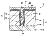
도 4a에 나타내는 바와 같이, 웨이퍼(W)에는 금속인 배선(50)이 형성되고, 또한 이러한 배선(50) 상에 절연막(60)이 마련된다. 배선(50)은 예를 들면 Cu, Co, Ni 또는 Ru을 포함하는 도전성의 재료이다. As shown in Fig. 4a, a metal wiring (50) is formed on a wafer (W), and an insulating film (60) is provided on the wiring (50). The wiring (50) is a conductive material including, for example, Cu, Co, Ni, or Ru.
절연막(60)은 예를 들면 산화막(61)과 질화막(62)을 가진다. 그리고, 배선(50) 상에 질화막(62)이 정해진 두께로 형성되고, 이러한 질화막(62) 상에 산화막(61)이 정해진 두께로 형성된다. 질화막(62)은 예를 들면 배선(50)이 Cu 등의 산화막(61) 내를 확산되는 원소로 구성되는 경우에, 이러한 원소가 산화막(61) 내에 확산되지 않기 위한 배리어막으로서 기능한다. The insulating film (60) has, for example, an oxide film (61) and a nitride film (62). Then, the nitride film (62) is formed on the wiring (50) with a set thickness, and the oxide film (61) is formed on the nitride film (62) with a set thickness. The nitride film (62) functions as a barrier film to prevent, for example, the element that diffuses into the oxide film (61), such as Cu, when the wiring (50) is composed of such an element that diffuses into the oxide film (61).
또한, 웨이퍼(W)에는 절연막(60)에 있어서의 정해진 위치에 비아(70)가 형성된다. 이러한 비아(70)는 절연막(60)의 상면(63)으로부터 배선(50)까지 관통하도록 형성된다. 그리고, 비아(70)는 내면(71)을 가지고, 이러한 내면(71)은 측면(72)과 배선(50)이 노출되는 저면(73)을 포함한다. In addition, a via (70) is formed at a predetermined position in the insulating film (60) on the wafer (W). This via (70) is formed to penetrate from the upper surface (63) of the insulating film (60) to the wiring (50). In addition, the via (70) has an inner surface (71), and this inner surface (71) includes a side surface (72) and a bottom surface (73) where the wiring (50) is exposed.
여기서, 웨이퍼(W)의 절연막(60)에 비아(70)를 형성하는 방법으로서는, 종래 공지의 방법으로부터 적절히 채용할 수 있다. 구체적으로, 예를 들면 드라이 에칭 기술로서, 불소계 또는 염소계 가스 등을 이용한 범용적 기술을 적용할 수 있다. Here, as a method for forming a via (70) in an insulating film (60) of a wafer (W), a conventionally known method can be appropriately employed. Specifically, for example, a general-purpose technique using fluorine-based or chlorine-based gas, etc., as a dry etching technique can be applied.
특히, 애스펙트비(직경에 대한 깊이의 비율)의 큰 비아(70)를 형성하는 방법으로서, 고속의 심굴 에칭이 가능한 ICP-RIE(Inductively Coupled Plasma Reactive Ion Etching : 유도 결합 플라즈마-반응성 이온 에칭)의 기술을 채용할 수 있다. In particular, as a method for forming a via (70) with a large aspect ratio (ratio of depth to diameter), the technology of ICP-RIE (Inductively Coupled Plasma Reactive Ion Etching) capable of high-speed deep-hole etching can be adopted.
예를 들면, 육불화 유황(SF6)을 이용한 에칭 단계와 C4F8 등의 테플론(등록 상표)계 가스를 이용한 보호 단계를 반복하면서 행하는, 이른바 보쉬 프로세스를 적합하게 채용할 수 있다. For example, the so-called Bosch process can be suitably employed, which involves repeating an etching step using sulfur hexafluoride (SF 6 ) and a protection step using a Teflon (registered trademark) gas such as C 4 F 8 .
도 4a에 나타내는 바와 같이, 배선(50) 상의 절연막(60)에 비아(70)가 형성된 웨이퍼(W)는, 상술한 단분자막 형성 처리 유닛(16)으로 반입되어, 정해진 단분자막 형성 처리가 행해진다. 이러한 단분자막 형성 처리는, 진공 챔버 내에서 실란 커플링제 또는 티탄 커플링제 등의 커플링제를 기화시켜 흡착시킨다. As shown in Fig. 4a, a wafer (W) having a via (70) formed in an insulating film (60) on a wiring (50) is brought into the above-described monomolecular film formation processing unit (16), and a predetermined monomolecular film formation processing is performed. This monomolecular film formation processing is performed by vaporizing and adsorbing a coupling agent such as a silane coupling agent or a titanium coupling agent in a vacuum chamber.
이에 의해, 도 4b에 나타내는 바와 같이, 비아(70)의 저면(73)에 노출되는 배선(50) 상에, 단분자막(80)이 형성된다. 또한, 이러한 단분자막(80)은 금속에만 흡착하는 커플링제를 이용하여 형성되는 점에서, 배선(50) 상에만 형성되고, 절연막(60)의 표면에는 형성되지 않는다. Accordingly, as shown in Fig. 4b, a monolayer (80) is formed on the wiring (50) exposed to the bottom surface (73) of the via (70). In addition, since this monolayer (80) is formed using a coupling agent that only adsorbs to metal, it is formed only on the wiring (50) and not on the surface of the insulating film (60).
즉, 실시 형태에 따르면, 커플링제를 이용하여 단분자막(80)을 형성함으로써, 비아(70)의 저면(73)에 선택적으로 단분자막(80)을 형성할 수 있다. That is, according to the embodiment, by forming a monolayer (80) using a coupling agent, a monolayer (80) can be selectively formed on the bottom surface (73) of a via (70).
또한 실시 형태에서는, 진공 챔버 내에서 커플링제를 흡착시켜 단분자막(80)을 형성하는 예에 대하여 나타냈지만, 단분자막(80)을 형성하는 방법은 이러한 예에 한정되지 않는다. 예를 들면, 커플링제를 용해시킨 처리액을 웨이퍼(W) 상에 토출하고, 이러한 처리액이 토출된 웨이퍼(W)를 스핀시킴으로써 단분자막(80)을 형성해도 된다. In addition, in the embodiment, an example of forming a monolayer (80) by adsorbing a coupling agent in a vacuum chamber is shown, but the method of forming a monolayer (80) is not limited to this example. For example, a monolayer (80) may be formed by discharging a treatment solution containing a coupling agent dissolved therein onto a wafer (W) and spinning the wafer (W) onto which the treatment solution is discharged.
이어서, 단분자막(80)이 형성된 웨이퍼(W)는, 상술한 성막 처리 유닛(17)으로 반입되어, 정해진 배리어막 형성 처리가 행해진다. 이러한 배리어막 형성 처리는 PVD법 또는 CVD법 등의 범용적 기술을 이용하여 행해진다. Next, the wafer (W) on which the monolayer film (80) is formed is brought into the above-described film forming unit (17), and a predetermined barrier film forming process is performed. This barrier film forming process is performed using a general-purpose technique such as the PVD method or the CVD method.
이에 의해, 도 4c에 나타내는 바와 같이, 비아(70)의 측면(72) 및 절연막(60)의 상면(63)에, Co-W-B 합금 등으로 구성되는 배리어막(81)이 형성된다. 여기서, 단분자막(80)의 표면에서는 배리어막(81)의 형성이 저해되는 점에서, 비아(70)의 저면(73)에는 배리어막(81)은 형성되지 않는다. Accordingly, as shown in Fig. 4c, a barrier film (81) composed of a Co-W-B alloy or the like is formed on the side surface (72) of the via (70) and the upper surface (63) of the insulating film (60). Here, since the formation of the barrier film (81) is inhibited on the surface of the monolayer film (80), the barrier film (81) is not formed on the bottom surface (73) of the via (70).
또한, 실시 형태에서는 배리어막(81)이 Co-W-B 합금으로 구성되는 예에 대하여 나타냈지만, 배리어막(81)은 Co-W-B 합금에 한정되지 않고, 후술하는 무전해 도금막(82)(도 4e 참조) 또는 전해 도금막(84)(도 4g 참조)에 포함되는 원소가 산화막(61) 내에 확산되는 것을 방지할 수 있는 재료로 구성되어 있으면 된다. In addition, although the embodiment shows an example in which the barrier film (81) is composed of a Co-W-B alloy, the barrier film (81) is not limited to a Co-W-B alloy, and may be composed of a material capable of preventing an element included in an electroless plating film (82) (see FIG. 4e) or an electrolytic plating film (84) (see FIG. 4g) described later from diffusing into the oxide film (61).
또한 실시 형태에서는, 배리어막(81)이 PVD법 또는 CVD법 등의 드라이 프로세스로 형성되는 예에 대하여 나타냈지만, 배리어막(81)은 드라이 프로세스로 형성되는 경우에 한정되지 않고, 예를 들면 무전해 도금 처리 등의 웨트 프로세스로 형성되어도 된다. In addition, in the embodiment, an example in which the barrier film (81) is formed by a dry process such as a PVD method or a CVD method is shown, but the barrier film (81) is not limited to being formed by a dry process, and may be formed by a wet process such as an electroless plating process, for example.
이어서, 배리어막(81)이 형성된 웨이퍼(W)는, 상술한 무전해 도금 처리 유닛(18)으로 반입되어, 먼저 정해진 단분자막 제거 처리가 행해진다. 이러한 단분자막 제거 처리는, 예를 들면 무전해 도금 처리 유닛(18)의 제 1 처리액 공급 기구(32a)를 이용하여, 제 1 처리액인 TMAH가 웨이퍼(W) 상에 토출된다. Next, the wafer (W) on which the barrier film (81) is formed is brought into the electroless plating treatment unit (18) described above, and a predetermined monolayer film removal treatment is performed first. In this monolayer film removal treatment, for example, the first treatment liquid, TMAH, is discharged onto the wafer (W) using the first treatment liquid supply mechanism (32a) of the electroless plating treatment unit (18).
이에 의해, 도 4d에 나타내는 바와 같이, 비아(70)의 저면(73)에 형성되어 있던 단분자막(80)이 용해되어 제거된다. 또한, 실시 형태에서는 단분자막(80)을 TMAH로 제거한 예에 대하여 나타냈지만, 제거하는 처리액은 TMAH에 한정되지 않는다. 또한, 단분자막 제거 처리에서는, 단분자막(80)을 고열로 열분해하여 제거해도 되고, 단분자막(80)을 플라즈마로 날려 제거해도 된다. By this, as shown in Fig. 4d, the monolayer film (80) formed on the bottom surface (73) of the via (70) is dissolved and removed. In addition, although the embodiment shows an example in which the monolayer film (80) is removed with TMAH, the removal treatment solution is not limited to TMAH. In addition, in the monolayer removal treatment, the monolayer film (80) may be removed by thermal decomposition at high temperature, or the monolayer film (80) may be removed by blowing it away with plasma.
이어서, 단분자막(80)이 제거된 웨이퍼(W)에, 정해진 무전해 도금 처리가 행해진다. 이러한 무전해 도금 처리는, 예를 들면 무전해 도금 처리 유닛(18)의 제 2 처리액 공급 기구(32b)를 이용하여, 제 2 처리액인 무전해 도금액이 웨이퍼(W) 상에 토출된다. Next, a predetermined electroless plating process is performed on the wafer (W) from which the monolayer film (80) has been removed. In this electroless plating process, for example, a second processing liquid, an electroless plating liquid, is discharged onto the wafer (W) using a second processing liquid supply mechanism (32b) of the electroless plating processing unit (18).
이에 의해, 도 4e에 나타내는 바와 같이, 비아(70)의 저면(73)에 노출되는 배선(50)을 촉매로 하여, 비아(70)의 저면(73)으로부터 보텀 업하여 무전해 도금막(82)이 형성된다. 또한 실시 형태에서는, 비아(70)의 저부 근방을 포함하는 하부에 무전해 도금막(82)이 형성된다. Accordingly, as shown in Fig. 4e, an electroless plating film (82) is formed from the bottom up from the bottom surface (73) of the via (70) using the wiring (50) exposed to the bottom surface (73) of the via (70) as a catalyst. In addition, in the embodiment, an electroless plating film (82) is formed in the lower portion including the vicinity of the bottom of the via (70).
이와 같이, 저면(73)에 노출시킨 배선(50)을 촉매로 하여, 저면(73)으로부터 보텀 업하여 무전해 도금막(82)을 형성함으로써, 애스펙트비가 크고 금속 배선을 형성하기 어려운 비아(70)의 저부 근방에, 보이드 또는 심 등이 포함되지 않는 양호한 금속 배선을 형성할 수 있다. In this way, by forming an electroless plating film (82) from the bottom up from the bottom surface (73) using the wiring (50) exposed on the bottom surface (73) as a catalyst, it is possible to form a good metal wiring that does not include a void or core near the bottom of a via (70) where the aspect ratio is large and it is difficult to form a metal wiring.
또한 실시 형태에서는, 배선(50)을 촉매로 하여 무전해 도금막(82)을 형성하는 점에서, 배리어막 또는 시드막 등을 개재하지 않고, 배선(50)과 무전해 도금막(82)을 직접 컨택시킬 수 있다. 이에 의해, 비아(70)의 내부에 형성되는 금속 배선의 전기 저항을 저감시킬 수 있다. In addition, in the embodiment, since the electroless plating film (82) is formed using the wiring (50) as a catalyst, the wiring (50) and the electroless plating film (82) can be brought into direct contact without intervening a barrier film or seed film, etc. As a result, the electrical resistance of the metal wiring formed inside the via (70) can be reduced.
실시 형태에서는, 무전해 도금막(82)이 Cu, Co, Ni 또는 Ru을 포함하면 된다. 이에 의해, Cu, Co, Ni 또는 Ru을 포함하는 배선(50)을 촉매로 하여, 비아(70)의 저면(73)으로부터 효율 좋게 무전해 도금막(82)을 형성할 수 있다. In the embodiment, the electroless plating film (82) may include Cu, Co, Ni or Ru. Accordingly, the electroless plating film (82) can be efficiently formed from the bottom surface (73) of the via (70) using the wiring (50) including Cu, Co, Ni or Ru as a catalyst.
이어서, 무전해 도금막(82)이 형성된 웨이퍼(W)는, 상술한 성막 처리 유닛(17)으로 반입되어, 정해진 시드막 형성 처리가 행해진다. 이러한 시드막 형성 처리는 PVD법 또는 CVD법 등의 범용적 기술을 이용하여 행해진다. Next, the wafer (W) on which the electroless plating film (82) is formed is brought into the film forming unit (17) described above, and a predetermined seed film forming process is performed. This seed film forming process is performed using a general-purpose technology such as the PVD method or the CVD method.
이에 의해, 도 4f에 나타내는 바와 같이 비아(70)의 내면(71) 및 절연막(60)의 상면(63)에 시드막(83)이 형성된다. 시드막(83)은 후술하는 전해 도금막(84)(도 4g참조)을 형성할 시의 촉매로서 기능하는 재료로 구성된다. 예를 들면, 전해 도금막(84)이 Cu 또는 Cu 합금인 경우, 시드막(83)은 Cu를 포함하면 되고, 전해 도금막(84)이 Co 또는 Co 합금인 경우, 시드막(83)은 Co를 포함하면 된다. By this, as shown in Fig. 4f, a seed film (83) is formed on the inner surface (71) of the via (70) and the upper surface (63) of the insulating film (60). The seed film (83) is composed of a material that functions as a catalyst when forming an electrolytic plating film (84) (see Fig. 4g) described later. For example, when the electrolytic plating film (84) is Cu or a Cu alloy, the seed film (83) may contain Cu, and when the electrolytic plating film (84) is Co or a Co alloy, the seed film (83) may contain Co.
이어서, 시드막(83)이 형성된 웨이퍼(W)는, 상술한 전해 도금 처리 유닛(19)으로 반입되어, 먼저 정해진 세정 처리가 행해진다. 이러한 세정 처리는, 예를 들면 처리액 공급 기구(43)의 노즐(43a)을 이용하여, 세정액인 DHF가 웨이퍼(W) 상에 토출된다. Next, the wafer (W) on which the seed film (83) is formed is brought into the electrolytic plating treatment unit (19) described above, and a predetermined cleaning treatment is first performed. In this cleaning treatment, for example, a cleaning solution, DHF, is discharged onto the wafer (W) using a nozzle (43a) of a treatment solution supply mechanism (43).
이에 의해, 시드막(83)의 표면에 형성된 자연 산화막 및 부착물 등이 제거되는 점에서, 시드막(83)의 표면을 청정한 상태로 할 수 있다. By this, the surface of the seed film (83) can be made clean by removing the natural oxide film and attachments formed on the surface of the seed film (83).
이어서, 세정 처리된 웨이퍼(W)에, 정해진 전해 도금 처리가 행해진다. 이러한 전해 도금 처리는, 예를 들면 먼저 도 3에 나타낸 전해 도금 처리 유닛(19)에 있어서의 처리액 공급 기구(43)의 노즐(43b)을 이용하여, 전해 도금액을 웨이퍼(W) 상에 액 축적한다. Next, a predetermined electrolytic plating process is performed on the cleaned wafer (W). This electrolytic plating process is performed by, for example, first accumulating the electrolytic plating solution on the wafer (W) using the nozzle (43b) of the processing solution supply mechanism (43) in the electrolytic plating process unit (19) shown in Fig. 3.
이어서, 이동 기구(41d)에 의해 전해 처리부(41) 전체를 기판 유지부(40)에 유지된 웨이퍼(W)에 근접시켜, 접촉 단자(41c)의 선단부를 웨이퍼(W)의 외주부에 접촉시킨다. 또한 그 때, 웨이퍼(W)에 액 축적된 전해 도금액에 직접 전극(41b)을 직접 접촉시킨다. Next, the entire electrolytic treatment section (41) is brought close to the wafer (W) held by the substrate holding section (40) by the moving mechanism (41d), and the tip of the contact terminal (41c) is brought into contact with the outer peripheral portion of the wafer (W). In addition, at that time, the electrode (41b) is brought into direct contact with the electrolytic plating liquid accumulated on the wafer (W).
그리고, 전압 인가부(42)의 스위치(42b)와 스위치(42c)를 동시에 오프 상태에서 온 상태로 변경함으로써, 직접 전극(41b)을 양극으로 하고, 웨이퍼(W)를 음극으로 하도록 웨이퍼(W)와 전해 도금액에 전압을 인가하여, 직접 전극(41b)과 웨이퍼(W)와의 사이에 전류를 흘린다. And, by simultaneously changing the switch (42b) and the switch (42c) of the voltage application unit (42) from the off state to the on state, voltage is applied to the wafer (W) and the electrolytic plating solution so that the direct electrode (41b) becomes the anode and the wafer (W) becomes the cathode, thereby causing current to flow between the direct electrode (41b) and the wafer (W).
이에 의해, 웨이퍼(W)의 표면에 금속 이온이 환원되어, 도 4g에 나타내는 바와 같이, 시드막(83)을 촉매로 하여 시드막(83)의 표면에 전해 도금막(84)이 석출되고, 비아(70)의 내부가 전해 도금막(84)으로 매립된다. 예를 들면, Cu를 포함하는 전해 도금액을 이용함으로써 Cu를 포함하는 전해 도금막(84)을 형성할 수 있고, Co를 포함하는 전해 도금액을 이용함으로써 Co를 포함하는 전해 도금막(84)을 형성할 수 있다. Thereby, the metal ions on the surface of the wafer (W) are reduced, and as shown in Fig. 4g, an electrolytic plating film (84) is deposited on the surface of the seed film (83) using the seed film (83) as a catalyst, and the interior of the via (70) is filled with the electrolytic plating film (84). For example, by using an electrolytic plating solution containing Cu, an electrolytic plating film (84) containing Cu can be formed, and by using an electrolytic plating solution containing Co, an electrolytic plating film (84) containing Co can be formed.
여기까지 설명한 각종 처리에 의해, 실시 형태에 따르면, 애스펙트비가 높은 비아(70)의 내부를 양호한 금속 배선으로 매립할 수 있다. By the various processes described so far, according to the embodiment, the interior of a high aspect ratio via (70) can be filled with good metal wiring.
<다층 배선의 형성 처리의 상세><Details of multilayer wiring formation process>
이어서, 도 5를 참조하여, 실시 형태에 따른 다층 배선의 형성 처리의 상세에 대하여 설명한다. 도 5는 실시 형태에 따른 다층 배선의 형성 처리에 있어서의 처리 순서를 나타내는 순서도이다. Next, with reference to Fig. 5, details of the formation process of the multilayer wiring according to the embodiment will be described. Fig. 5 is a flowchart showing the processing sequence in the formation process of the multilayer wiring according to the embodiment.
또한, 도 5에 나타내는 다층 배선의 형성 처리는, 실시 형태에 따른 기억 매체로부터 기억부(22)에 인스톨된 프로그램을 제어부(21)가 읽어내고, 읽어낸 명령에 기초하여 제어부(21)가 반송부(15) 및 단분자막 형성 처리 유닛(16), 성막 처리 유닛(17), 무전해 도금 처리 유닛(18), 전해 도금 처리 유닛(19) 등을 제어함으로써 실행된다. In addition, the formation process of the multilayer wiring shown in Fig. 5 is executed by the control unit (21) reading a program installed in the memory unit (22) from the memory medium according to the embodiment, and the control unit (21) controlling the return unit (15), the monolayer film formation processing unit (16), the film formation processing unit (17), the electroless plating processing unit (18), the electrolytic plating processing unit (19), etc. based on the read command.
먼저, 캐리어(C)로부터, 기판 반송 장치(13)와, 전달부(14)와, 기판 반송 장치(20)를 경유하여, 배선(50) 상의 절연막(60)에 비아(70)가 형성된 웨이퍼(W)를 단분자막 형성 처리 유닛(16)의 내부로 반송한다. First, a wafer (W) with a via (70) formed in an insulating film (60) on a wiring (50) is returned from a carrier (C) to the inside of a monolayer film formation processing unit (16) via a substrate return device (13), a transfer unit (14), and a substrate return device (20).
이어서, 제어부(21)는 단분자막 형성 처리 유닛(16)을 제어하여, 웨이퍼(W)에 대하여 단분자막 형성 처리를 행하여, 비아(70)의 저면(73)에 단분자막(80)을 형성한다(단계(S101)). 이러한 단분자막 형성 처리는, 예를 들면, 진공 챔버 내에서 실란 커플링제 또는 티탄 커플링제 등의 커플링제를 기화시켜 흡착시킴으로써 행해진다. Next, the control unit (21) controls the monolayer formation processing unit (16) to perform monolayer formation processing on the wafer (W) to form a monolayer (80) on the bottom surface (73) of the via (70) (step (S101)). This monolayer formation processing is performed, for example, by vaporizing and adsorbing a coupling agent such as a silane coupling agent or a titanium coupling agent in a vacuum chamber.
이어서, 제어부(21)는 기판 반송 장치(20)를 제어하여, 웨이퍼(W)를 단분자막 형성 처리 유닛(16)으로부터 성막 처리 유닛(17)으로 반송한다. 그리고, 제어부(21)는 성막 처리 유닛(17)을 제어하여, 웨이퍼(W)에 대하여 배리어막 형성 처리를 행하여, 비아(70)의 측면(72) 및 절연막(60)의 상면(63)에 배리어막(81)을 형성한다(단계(S102)). Next, the control unit (21) controls the substrate return device (20) to return the wafer (W) from the monolayer film formation processing unit (16) to the film formation processing unit (17). Then, the control unit (21) controls the film formation processing unit (17) to perform a barrier film formation processing on the wafer (W), thereby forming a barrier film (81) on the side surface (72) of the via (70) and the upper surface (63) of the insulating film (60) (step (S102)).
이러한 배리어막 형성 처리는, 예를 들면 PVD법 또는 CVD법 등의 범용적 기술을 이용하여, 웨이퍼(W)에 Co-W-B 합금 등의 배리어막(81)을 성막함으로써 행해진다. This barrier film formation process is performed by forming a barrier film (81) of a Co-W-B alloy or the like on a wafer (W) using a general-purpose technique such as a PVD method or a CVD method.
이어서, 제어부(21)는 기판 반송 장치(20)를 제어하여, 웨이퍼(W)를 성막 처리 유닛(17)으로부터 무전해 도금 처리 유닛(18)으로 반송한다. 그리고, 제어부(21)는 무전해 도금 처리 유닛(18)을 제어하여, 웨이퍼(W)에 대하여 단분자막 제거 처리를 행하여, 비아(70)의 저면(73)으로부터 단분자막(80)을 제거한다(단계(S103)). Next, the control unit (21) controls the substrate return device (20) to return the wafer (W) from the film forming treatment unit (17) to the electroless plating treatment unit (18). Then, the control unit (21) controls the electroless plating treatment unit (18) to perform a monolayer removal treatment on the wafer (W), thereby removing the monolayer (80) from the bottom surface (73) of the via (70) (step (S103)).
이러한 단분자막 제거 처리는, 예를 들면 웨이퍼(W) 상에 TMAH를 토출하고, 이러한 TMAH로 비아(70)의 저면(73)에 형성되는 단분자막(80)을 용해함으로써 행해진다. This monolayer film removal treatment is performed, for example, by discharging TMAH on a wafer (W) and dissolving the monolayer film (80) formed on the bottom surface (73) of the via (70) with this TMAH.
이어서, 제어부(21)는 무전해 도금 처리 유닛(18)을 제어하여, 웨이퍼(W)에 대하여 무전해 도금 처리를 행하여, 비아(70)의 저면(73)으로부터 무전해 도금막(82)을 형성한다(단계(S104)). Next, the control unit (21) controls the electroless plating treatment unit (18) to perform electroless plating treatment on the wafer (W) and form an electroless plating film (82) from the bottom surface (73) of the via (70) (step (S104)).
이러한 무전해 도금 처리는, 예를 들면 웨이퍼(W) 상에 무전해 도금액을 토출하고, 저면(73)에 노출되는 배선(50)을 촉매로 하여, 토출된 무전해 도금액으로 저면(73)으로부터 보텀 업하여 무전해 도금막(82)을 형성함으로써 행해진다. This electroless plating process is performed, for example, by discharging an electroless plating solution on a wafer (W), and using the wiring (50) exposed on the lower surface (73) as a catalyst, forming an electroless plating film (82) from the lower surface (73) upward with the discharged electroless plating solution.
이어서, 제어부(21)는 기판 반송 장치(20)를 제어하여, 웨이퍼(W)를 무전해 도금 처리 유닛(18)으로부터 성막 처리 유닛(17)으로 반송한다. 그리고, 제어부(21)는 성막 처리 유닛(17)을 제어하여, 웨이퍼(W)에 대하여 시드막 형성 처리를 행하여, 비아(70)의 내면(71) 및 절연막(60)의 상면(63)에 시드막(83)을 형성한다(단계(S105)). Next, the control unit (21) controls the substrate return device (20) to return the wafer (W) from the electroless plating treatment unit (18) to the film formation treatment unit (17). Then, the control unit (21) controls the film formation treatment unit (17) to perform seed film formation treatment on the wafer (W), thereby forming a seed film (83) on the inner surface (71) of the via (70) and the upper surface (63) of the insulating film (60) (step (S105)).
이러한 시드막 형성 처리는, 예를 들면 PVD법 또는 CVD법 등의 범용적 기술을 이용하여, 웨이퍼(W)에 Cu 또는 Co 등을 포함하는 시드막(83)을 성막함으로써 행해진다. This seed film formation process is performed by forming a seed film (83) containing Cu or Co, etc. on a wafer (W) using a general-purpose technique such as a PVD method or a CVD method.
이어서, 제어부(21)는 기판 반송 장치(20)를 제어하여, 웨이퍼(W)를 성막 처리 유닛(17)으로부터 전해 도금 처리 유닛(19)으로 반송한다. 그리고, 제어부(21)는 전해 도금 처리 유닛(19)을 제어하여, 웨이퍼(W)에 대하여 세정 처리를 행하여, 웨이퍼(W)를 세정한다(단계(S106)). Next, the control unit (21) controls the substrate return device (20) to return the wafer (W) from the film forming treatment unit (17) to the electroplating treatment unit (19). Then, the control unit (21) controls the electroplating treatment unit (19) to perform a cleaning treatment on the wafer (W), thereby cleaning the wafer (W) (step (S106)).
이러한 세정 처리는, 예를 들면 웨이퍼(W) 상에 DHF를 토출하여, 이러한 DHF로 시드막(83)의 표면에 형성되는 자연 산화막 및 부착물 등을 제거함으로써 행해진다. This cleaning treatment is performed, for example, by discharging DHF onto a wafer (W) and removing a natural oxide film and attachments formed on the surface of the seed film (83) with this DHF.
이어서, 제어부(21)는 전해 도금 처리 유닛(19)을 제어하여, 웨이퍼(W)에 대하여 전해 도금 처리를 행하여, 비아(70)의 내부를 전해 도금막(84)으로 매립한다(단계(S107)). Next, the control unit (21) controls the electrolytic plating treatment unit (19) to perform electrolytic plating treatment on the wafer (W) and fill the inside of the via (70) with an electrolytic plating film (84) (step (S107)).
이러한 전해 도금 처리는, 예를 들면 웨이퍼(W) 상에 전해 도금액을 액 축적하고, 접촉 단자(41c)의 선단부를 웨이퍼(W)의 외주부에 접촉시키고 또한 전해 도금액에 직접 전극(41b)을 직접 접촉시킨다. This electrolytic plating treatment is performed by, for example, accumulating an electrolytic plating solution on a wafer (W), contacting the tip of a contact terminal (41c) with the outer peripheral portion of the wafer (W), and also directly contacting an electrode (41b) with the electrolytic plating solution.
그리고, 전해 도금 처리는 직접 전극(41b)을 양극으로 하고, 웨이퍼(W)를 음극으로 하도록 웨이퍼(W)와 전해 도금액에 전압을 인가하여, 직접 전극(41b)과 웨이퍼(W) 사이에 전류를 흘림으로써 행해진다. 이러한 전해 도금 처리가 완료되면, 웨이퍼(W)에 대한 다층 배선의 형성 처리가 완료된다. And, the electrolytic plating process is performed by applying voltage to the wafer (W) and the electrolytic plating solution so that the direct electrode (41b) becomes the anode and the wafer (W) becomes the cathode, thereby causing current to flow between the direct electrode (41b) and the wafer (W). When this electrolytic plating process is completed, the formation process of the multilayer wiring for the wafer (W) is completed.
이상, 본 발명의 실시 형태에 대하여 설명했지만, 본 발명은 상기 실시 형태에 한정되는 것이 아니며, 그 취지를 일탈하지 않는 한에 있어서 각종 변경이 가능하다. 예를 들면, 상술한 실시 형태에서는, 비아(70)의 저부 근방에 무전해 도금막(82)을 형성하고, 이 후 전해 도금막(84)으로 비아(70)의 내부를 매립하는 예에 대하여 나타냈지만, 무전해 도금막(82)만으로 비아(70)의 내부를 매립해도 된다. Hereinafter, the embodiments of the present invention have been described, but the present invention is not limited to the above embodiments, and various modifications are possible without departing from the spirit thereof. For example, in the above-described embodiments, an example has been described in which an electroless plating film (82) is formed near the bottom of a via (70), and then the interior of the via (70) is filled with an electrolytic plating film (84), but the interior of the via (70) may be filled with only the electroless plating film (82).
또한 상술한 실시 형태에서는, 전해 도금액을 웨이퍼(W) 상에 액 축적하여 전해 도금 처리를 행한 예에 대하여 나타냈지만, 전해 도금 처리는 이러한 예에 한정되지 않는다. 예를 들면, 전해 도금액이 모인 전해조 내에 웨이퍼(W)를 침지시킴으로써 전해 도금 처리를 행해도 된다. In addition, in the above-described embodiment, an example was shown in which an electrolytic plating solution was accumulated on a wafer (W) and electrolytic plating treatment was performed, but the electrolytic plating treatment is not limited to this example. For example, an electrolytic plating treatment may be performed by immersing the wafer (W) in an electrolytic tank in which an electrolytic plating solution has been accumulated.
또한 상술한 실시 형태에 있어서, 무전해 도금막(82) 또는 전해 도금막(84)이 형성된 후에, 핫 플레이트 등으로 정해진 소성 처리를 실시함으로써, 무전해 도금막(82) 또는 전해 도금막(84)의 전기 저항을 저감시켜도 된다. In addition, in the above-described embodiment, after the electroless plating film (82) or the electrolytic plating film (84) is formed, the electrical resistance of the electroless plating film (82) or the electrolytic plating film (84) may be reduced by performing a prescribed firing treatment using a hot plate or the like.
실시 형태에 따른 다층 배선의 형성 방법은, 매립형의 다층 배선의 형성 방법으로서, 기판(웨이퍼(W))의 배선(50) 상에 마련되는 절연막(60)의 정해진 위치에 형성되어 배선(50)까지 관통하는 비아(70)에 있어서, 배선(50)이 노출되는 저면(73)에 단분자막(80)을 형성하는 공정(단계(S101))과, 비아(70)의 측면(72)에 배리어막(81)을 형성하는 공정(단계(S102))과, 단분자막(80)을 제거하는 공정(단계(S103))과, 비아(70)의 저면(73)에 노출되는 배선(50)을 촉매로 하여, 비아(70)의 저면(73)으로부터 무전해 도금막(82)을 형성하는 공정(단계(S104))을 포함한다. 이에 의해, 애스펙트비가 높은 비아(70)의 저부 근방에, 보이드 또는 심 등이 포함되지 않는 양호한 금속 배선을 형성할 수 있다. A method for forming a multilayer wiring according to an embodiment is a method for forming a buried multilayer wiring, and includes a step (step (S101)) of forming a monolayer film (80) on a bottom surface (73) of a via (70) that is formed at a predetermined position of an insulating film (60) provided on a wiring (50) of a substrate (wafer (W)) and penetrates up to the wiring (50), a step (step (S102)) of forming a barrier film (81) on a side surface (72) of the via (70), a step (step (S103)) of removing the monolayer film (80), and a step (step (S104)) of forming an electroless plating film (82) from the bottom surface (73) of the via (70) using the wiring (50) exposed on the bottom surface (73) of the via (70) as a catalyst. By this, it is possible to form a good metal wiring that does not include voids or cores near the bottom of a high aspect ratio via (70).
또한 실시 형태에 따른 다층 배선의 형성 방법에 있어서, 단분자막(80)은 커플링제에 의해 형성된다. 이에 의해, 비아(70)의 저면(73)에 선택적으로 단분자막(80)을 형성할 수 있다. In addition, in the method for forming a multilayer wiring according to the embodiment, a monolayer film (80) is formed by a coupling agent. As a result, a monolayer film (80) can be selectively formed on the bottom surface (73) of a via (70).
또한 실시 형태에 따른 다층 배선의 형성 방법에 있어서, 무전해 도금막(82)은 Cu, Co, Ni 또는 Ru을 포함한다. 이에 의해, Cu, Co, Ni 또는 Ru을 포함하는 배선(50)을 촉매로 하여, 비아(70)의 저면(73)으로부터 효율 좋게 무전해 도금막(82)을 형성할 수 있다. In addition, in the method for forming a multilayer wiring according to the embodiment, the electroless plating film (82) includes Cu, Co, Ni or Ru. Accordingly, the electroless plating film (82) can be efficiently formed from the bottom surface (73) of the via (70) using the wiring (50) including Cu, Co, Ni or Ru as a catalyst.
또한 실시 형태에 따른 기억 매체는, 컴퓨터 상에서 동작하고, 다층 배선 형성 시스템(1)을 제어하는 프로그램이 기억된 컴퓨터 독해 가능한 기억 매체로서, 프로그램은, 실행 시에, 상기에 기재된 다층 배선의 형성 방법이 행해지도록, 컴퓨터에 다층 배선 형성 시스템(1)을 제어시킨다. 이에 의해, 애스펙트비가 높은 비아(70)의 저부 근방에, 보이드 또는 심 등이 포함되지 않는 양호한 금속 배선을 형성할 수 있다. In addition, a storage medium according to an embodiment is a computer-readable storage medium storing a program that operates on a computer and controls a multilayer wiring formation system (1), wherein the program, when executed, causes the computer to control the multilayer wiring formation system (1) so that the above-described method for forming a multilayer wiring is performed. As a result, a good metal wiring that does not include a void or a core, etc., can be formed near the bottom of a via (70) having a high aspect ratio.
새로운 효과 및 변형예는, 당업자에 의해 용이하게 돌출될 수 있다. 이 때문에, 본 발명의 보다 광범위한 태양은 이상과 같이 나타내고 또한 기술한 특정의 상세 및 대표적인 실시 형태에 한정되는 것은 아니다. 따라서, 첨부의 청구의 범위 및 그 균등물에 의해 정의되는 총괄적인 발명의 개념의 정신 또는 범위로부터 일탈하지 않고, 다양한 변경이 가능하다. New effects and modifications can be easily suggested by those skilled in the art. Therefore, the broader aspects of the present invention are not limited to the specific details and representative embodiments shown and described above. Accordingly, various modifications are possible without departing from the spirit or scope of the overall inventive concept defined by the appended claims and their equivalents.
삭제delete
Claims (4)
기판의 배선 상에 마련되는 절연막의 정해진 위치에 형성되어 상기 배선까지 관통하는 비아에 있어서, 상기 배선이 노출되는 저면에 단분자막을 형성하며, 상기 절연막은 상기 배선 상에 형성된 질화막과 상기 질화막 상에 형성된 산화막으로 형성되는 공정과,
상기 비아의 측면에 Co-W-B 합금으로 형성된 배리어막을 형성하되, 상기 배리어막은 상기 단분자막이 형성된 상기 저면 상에는 형성되지 않는, 공정과,
상기 단분자막을 TMAH(Tetramethyl ammonium hydroxide)를 함유하는 처리액으로 제거하는 공정과,
상기 비아의 저면에 노출되는 상기 배선을 촉매로 하여, 상기 비아의 저면으로부터 무전해 도금막을 형성하는 공정을 포함하고,
상기 단분자막을 제거하는 공정 및 상기 무전해 도금막을 형성하는 공정은 동일한 하우징 또는 동일한 컵에서 실행되는 다층 배선의 형성 방법.A method for forming a multilayer wiring of the built-in type,
A process in which a monolayer is formed on a bottom surface where the wiring is exposed in a via formed at a predetermined location of an insulating film provided on the wiring of a substrate and penetrating to the wiring, and the insulating film is formed by a nitride film formed on the wiring and an oxide film formed on the nitride film;
A process for forming a barrier film formed of a Co-WB alloy on the side of the above via, wherein the barrier film is not formed on the bottom surface on which the monolayer film is formed.
A process for removing the above monolayer film with a treatment solution containing TMAH (Tetramethyl ammonium hydroxide),
A process for forming an electroless plating film from the bottom surface of the via using the wiring exposed to the bottom surface of the via as a catalyst,
A method for forming multilayer wiring, wherein the process for removing the above-mentioned monolayer film and the process for forming the above-mentioned electroless plating film are performed in the same housing or the same cup.
상기 단분자막은 커플링제에 의해 형성되는 다층 배선의 형성 방법. In paragraph 1,
The above monolayer film is a method for forming a multilayer wiring formed by a coupling agent.
상기 무전해 도금막은 Cu, Co, Ni 또는 Ru을 포함하는 다층 배선의 형성 방법. In claim 1 or 2,
The above electroless plating film is a method for forming a multilayer wiring including Cu, Co, Ni or Ru.
상기 프로그램은, 실행 시에, 제 1 항 또는 제 2 항에 기재된 다층 배선의 형성 방법이 행해지도록, 컴퓨터에 상기 다층 배선 형성 시스템을 제어시키는 것
을 특징으로 하는 기억 매체.A computer-readable storage medium storing a program that operates on a computer and controls a multilayer wiring formation system,
The above program, when executed, controls the multilayer wiring formation system on a computer so that the method for forming multilayer wiring described in claim 1 or claim 2 is performed.
A memory medium characterized by .
Applications Claiming Priority (3)
| Application Number | Priority Date | Filing Date | Title |
|---|---|---|---|
| JPJP-P-2018-016059 | 2018-02-01 | ||
| JP2018016059 | 2018-02-01 | ||
| PCT/JP2019/002070 WO2019151078A1 (en) | 2018-02-01 | 2019-01-23 | Method for forming multilayer wiring, and storage medium |
Publications (2)
| Publication Number | Publication Date |
|---|---|
| KR20200111253A KR20200111253A (en) | 2020-09-28 |
| KR102822263B1 true KR102822263B1 (en) | 2025-06-19 |
Family
ID=67478241
Family Applications (1)
| Application Number | Title | Priority Date | Filing Date |
|---|---|---|---|
| KR1020207024983A Active KR102822263B1 (en) | 2018-02-01 | 2019-01-23 | Method for forming multilayer wiring and memory medium |
Country Status (6)
| Country | Link |
|---|---|
| US (1) | US20210358767A1 (en) |
| JP (1) | JP6903171B2 (en) |
| KR (1) | KR102822263B1 (en) |
| CN (1) | CN111630654A (en) |
| TW (1) | TWI857945B (en) |
| WO (1) | WO2019151078A1 (en) |
Families Citing this family (6)
| Publication number | Priority date | Publication date | Assignee | Title |
|---|---|---|---|---|
| JP7399258B2 (en) * | 2020-03-02 | 2023-12-15 | 東京エレクトロン株式会社 | Plating processing equipment |
| EP4268274A4 (en) | 2020-12-28 | 2024-10-30 | Adeia Semiconductor Bonding Technologies Inc. | STRUCTURES WITH SUBSTRATE PASSAGES AND METHODS FOR FORMING THE SAME |
| KR20230125309A (en) | 2020-12-28 | 2023-08-29 | 아데이아 세미컨덕터 본딩 테크놀로지스 인코포레이티드 | Structures having through-substrate vias and methods for forming the same |
| TWI887524B (en) * | 2021-02-26 | 2025-06-21 | 日商Jsr股份有限公司 | Method for manufacturing multi-layer wiring board, kit for forming laminated film, and composition |
| JP2024051331A (en) | 2022-09-30 | 2024-04-11 | 東京エレクトロン株式会社 | SUBSTRATE PROCESSING METHOD AND SUBSTRATE PROCESSING SYSTEM |
| US20250112123A1 (en) * | 2023-09-29 | 2025-04-03 | Adeia Semiconductor Bonding Technologies Inc. | Through substrate via structures and processes |
Citations (7)
| Publication number | Priority date | Publication date | Assignee | Title |
|---|---|---|---|---|
| US20030134047A1 (en) * | 2002-01-16 | 2003-07-17 | Dubin Valery M | Apparatus and method for electroless spray deposition |
| US20050271975A1 (en) | 2003-12-15 | 2005-12-08 | Worcester Polytechnic Institute | Films with photoresponsive wettability |
| US20100003399A1 (en) * | 2008-07-01 | 2010-01-07 | C. Uyemura & Co., Ltd. | Electroless plating solution, method for electroless plating using the same and method for manufacturing circuit board |
| US20150380302A1 (en) * | 2014-06-30 | 2015-12-31 | Lam Research Corporation | Selective formation of dielectric barriers for metal interconnects in semiconductor devices |
| US20160190040A1 (en) * | 2014-12-25 | 2016-06-30 | Tokyo Electron Limited | Wiring layer forming method, wiring layer forming system and recording medium |
| US20170100955A1 (en) | 2014-06-05 | 2017-04-13 | Dai Nippon Printing Co., Ltd. | Producing method for printing plate, producing method for functional element, and printing apparatus |
| US20170141199A1 (en) * | 2015-11-18 | 2017-05-18 | Imec Vzw | Method for Forming a Field Effect Transistor Device Having an Electrical Contact |
Family Cites Families (17)
| Publication number | Priority date | Publication date | Assignee | Title |
|---|---|---|---|---|
| US6001415A (en) * | 1997-12-03 | 1999-12-14 | Advanced Micro Devices, Inc. | Via with barrier layer for impeding diffusion of conductive material from via into insulator |
| JP2001323381A (en) * | 2000-05-16 | 2001-11-22 | Sony Corp | Plating method and plating structure |
| JP2002026055A (en) * | 2000-07-12 | 2002-01-25 | Seiko Epson Corp | Semiconductor device and manufacturing method thereof |
| US7070687B2 (en) * | 2001-08-14 | 2006-07-04 | Intel Corporation | Apparatus and method of surface treatment for electrolytic and electroless plating of metals in integrated circuit manufacturing |
| JP2004146648A (en) * | 2002-10-25 | 2004-05-20 | Seiko Epson Corp | Semiconductor device and manufacturing method thereof |
| JP2004179589A (en) * | 2002-11-29 | 2004-06-24 | Sony Corp | Method for manufacturing semiconductor device |
| KR20050056378A (en) * | 2003-12-10 | 2005-06-16 | 매그나칩 반도체 유한회사 | Method of forming inductor in a semiconductor device |
| DE102006001253B4 (en) * | 2005-12-30 | 2013-02-07 | Advanced Micro Devices, Inc. | A method of forming a metal layer over a patterned dielectric by wet-chemical deposition with an electroless and a power controlled phase |
| CN102290372A (en) * | 2007-02-27 | 2011-12-21 | 株式会社爱发科 | Semiconductor device manufacturing method and semiconductor device manufacturing apparatus |
| JP5196467B2 (en) * | 2007-05-30 | 2013-05-15 | 東京エレクトロン株式会社 | Semiconductor device manufacturing method, semiconductor manufacturing apparatus, and storage medium |
| KR101096031B1 (en) * | 2009-03-31 | 2011-12-19 | 한양대학교 산학협력단 | Method of forming self-assembled monolayer and copper wiring of semiconductor device using same |
| WO2013100894A1 (en) * | 2011-12-27 | 2013-07-04 | Intel Corporation | Method of forming low resistivity tanx/ta diffusion barriers for backend interconnects |
| JP5968657B2 (en) | 2012-03-22 | 2016-08-10 | 東京エレクトロン株式会社 | Plating treatment method, plating treatment system, and storage medium |
| JP6054279B2 (en) * | 2013-10-17 | 2016-12-27 | 東京エレクトロン株式会社 | Metal wiring layer forming method, metal wiring layer forming apparatus, and storage medium |
| JP6100147B2 (en) * | 2013-11-21 | 2017-03-22 | 東京エレクトロン株式会社 | Plating pretreatment method and storage medium |
| JP6121348B2 (en) * | 2014-02-28 | 2017-04-26 | 東京エレクトロン株式会社 | Plating pretreatment method, storage medium, and plating treatment system |
| JP6411279B2 (en) * | 2015-05-11 | 2018-10-24 | 東京エレクトロン株式会社 | Plating process and storage medium |
-
2019
- 2019-01-23 WO PCT/JP2019/002070 patent/WO2019151078A1/en not_active Ceased
- 2019-01-23 KR KR1020207024983A patent/KR102822263B1/en active Active
- 2019-01-23 JP JP2019569045A patent/JP6903171B2/en active Active
- 2019-01-23 TW TW108102500A patent/TWI857945B/en active
- 2019-01-23 CN CN201980009315.3A patent/CN111630654A/en active Pending
- 2019-01-23 US US16/938,047 patent/US20210358767A1/en not_active Abandoned
Patent Citations (7)
| Publication number | Priority date | Publication date | Assignee | Title |
|---|---|---|---|---|
| US20030134047A1 (en) * | 2002-01-16 | 2003-07-17 | Dubin Valery M | Apparatus and method for electroless spray deposition |
| US20050271975A1 (en) | 2003-12-15 | 2005-12-08 | Worcester Polytechnic Institute | Films with photoresponsive wettability |
| US20100003399A1 (en) * | 2008-07-01 | 2010-01-07 | C. Uyemura & Co., Ltd. | Electroless plating solution, method for electroless plating using the same and method for manufacturing circuit board |
| US20170100955A1 (en) | 2014-06-05 | 2017-04-13 | Dai Nippon Printing Co., Ltd. | Producing method for printing plate, producing method for functional element, and printing apparatus |
| US20150380302A1 (en) * | 2014-06-30 | 2015-12-31 | Lam Research Corporation | Selective formation of dielectric barriers for metal interconnects in semiconductor devices |
| US20160190040A1 (en) * | 2014-12-25 | 2016-06-30 | Tokyo Electron Limited | Wiring layer forming method, wiring layer forming system and recording medium |
| US20170141199A1 (en) * | 2015-11-18 | 2017-05-18 | Imec Vzw | Method for Forming a Field Effect Transistor Device Having an Electrical Contact |
Also Published As
| Publication number | Publication date |
|---|---|
| CN111630654A (en) | 2020-09-04 |
| US20210358767A1 (en) | 2021-11-18 |
| TWI857945B (en) | 2024-10-11 |
| JP6903171B2 (en) | 2021-07-14 |
| WO2019151078A1 (en) | 2019-08-08 |
| JPWO2019151078A1 (en) | 2021-01-14 |
| TW201936986A (en) | 2019-09-16 |
| KR20200111253A (en) | 2020-09-28 |
Similar Documents
| Publication | Publication Date | Title |
|---|---|---|
| KR102822263B1 (en) | Method for forming multilayer wiring and memory medium | |
| US20140287580A1 (en) | Method for forming conductive structure, and plating apparatus and plating method | |
| KR20120117678A (en) | Liquid processing method, liquid processing apparatus, and storage medium | |
| KR102465644B1 (en) | Substrate processing apparatus, substrate processing method, and computer-readable recording medium | |
| CN114916234B (en) | Plating apparatus and plating method | |
| JP2005097732A (en) | Plating apparatus | |
| KR102772946B1 (en) | Method for forming multilayer wiring and memory medium | |
| KR20060048644A (en) | Method and apparatus for plating semiconductor wafers | |
| KR20160102895A (en) | Catalyst layer forming method, catalyst layer forming system and recording medium | |
| CN112585722B (en) | Substrate processing method and substrate processing device | |
| JP6910480B2 (en) | Multi-layer wiring forming method, multi-layer wiring forming device and storage medium | |
| CN110491799B (en) | Substrate processing apparatus and substrate processing method | |
| JP7614232B2 (en) | Plating method and plating apparatus | |
| CN100552872C (en) | Semiconductor substrate processing apparatus and method | |
| JP4010764B2 (en) | Substrate plating apparatus and plating method | |
| US20010037943A1 (en) | Liquid treatment equipment and liquid treatment method | |
| KR20250136365A (en) | Plating method and plating device | |
| TWI758006B (en) | Plating apparatus and plating treatment method | |
| KR20220139347A (en) | Plating processing method and plating processing apparatus | |
| WO2024252965A1 (en) | Substrate processing method, substrate processing device, and storage medium | |
| JP2008150631A (en) | Plating apparatus and plating method | |
| KR20250159222A (en) | Substrate processing device and cleaning method for substrate processing device | |
| JP2014533887A (en) | Machine for metallizing cavities in semi-conductive or conductive substrates such as through via structures |
Legal Events
| Date | Code | Title | Description |
|---|---|---|---|
| PA0105 | International application |
St.27 status event code: A-0-1-A10-A15-nap-PA0105 |
|
| P11-X000 | Amendment of application requested |
St.27 status event code: A-2-2-P10-P11-nap-X000 |
|
| P13-X000 | Application amended |
St.27 status event code: A-2-2-P10-P13-nap-X000 |
|
| PG1501 | Laying open of application |
St.27 status event code: A-1-1-Q10-Q12-nap-PG1501 |
|
| A201 | Request for examination | ||
| PA0201 | Request for examination |
St.27 status event code: A-1-2-D10-D11-exm-PA0201 |
|
| E902 | Notification of reason for refusal | ||
| PE0902 | Notice of grounds for rejection |
St.27 status event code: A-1-2-D10-D21-exm-PE0902 |
|
| P11-X000 | Amendment of application requested |
St.27 status event code: A-2-2-P10-P11-nap-X000 |
|
| P13-X000 | Application amended |
St.27 status event code: A-2-2-P10-P13-nap-X000 |
|
| E90F | Notification of reason for final refusal | ||
| PE0902 | Notice of grounds for rejection |
St.27 status event code: A-1-2-D10-D21-exm-PE0902 |
|
| P11-X000 | Amendment of application requested |
St.27 status event code: A-2-2-P10-P11-nap-X000 |
|
| P13-X000 | Application amended |
St.27 status event code: A-2-2-P10-P13-nap-X000 |
|
| E601 | Decision to refuse application | ||
| PE0601 | Decision on rejection of patent |
St.27 status event code: N-2-6-B10-B15-exm-PE0601 |
|
| P11-X000 | Amendment of application requested |
St.27 status event code: A-2-2-P10-P11-nap-X000 |
|
| PX0701 | Decision of registration after re-examination |
St.27 status event code: A-3-4-F10-F13-rex-PX0701 |
|
| X701 | Decision to grant (after re-examination) | ||
| PR1002 | Payment of registration fee |
St.27 status event code: A-2-2-U10-U12-oth-PR1002 Fee payment year number: 1 |
|
| PG1601 | Publication of registration |
St.27 status event code: A-4-4-Q10-Q13-nap-PG1601 |
|
| P22-X000 | Classification modified |
St.27 status event code: A-4-4-P10-P22-nap-X000 |