KR102822160B1 - Display driving integrated circuit of display device and method of operating the same - Google Patents
Display driving integrated circuit of display device and method of operating the same Download PDFInfo
- Publication number
- KR102822160B1 KR102822160B1 KR1020200173649A KR20200173649A KR102822160B1 KR 102822160 B1 KR102822160 B1 KR 102822160B1 KR 1020200173649 A KR1020200173649 A KR 1020200173649A KR 20200173649 A KR20200173649 A KR 20200173649A KR 102822160 B1 KR102822160 B1 KR 102822160B1
- Authority
- KR
- South Korea
- Prior art keywords
- data
- mode
- frame buffer
- display
- integrated circuit
- Prior art date
- Legal status (The legal status is an assumption and is not a legal conclusion. Google has not performed a legal analysis and makes no representation as to the accuracy of the status listed.)
- Active
Links
Images


Classifications
-
- G—PHYSICS
- G09—EDUCATION; CRYPTOGRAPHY; DISPLAY; ADVERTISING; SEALS
- G09G—ARRANGEMENTS OR CIRCUITS FOR CONTROL OF INDICATING DEVICES USING STATIC MEANS TO PRESENT VARIABLE INFORMATION
- G09G3/00—Control arrangements or circuits, of interest only in connection with visual indicators other than cathode-ray tubes
- G09G3/20—Control arrangements or circuits, of interest only in connection with visual indicators other than cathode-ray tubes for presentation of an assembly of a number of characters, e.g. a page, by composing the assembly by combination of individual elements arranged in a matrix no fixed position being assigned to or needed to be assigned to the individual characters or partial characters
- G09G3/2092—Details of a display terminals using a flat panel, the details relating to the control arrangement of the display terminal and to the interfaces thereto
- G09G3/2096—Details of the interface to the display terminal specific for a flat panel
-
- H—ELECTRICITY
- H04—ELECTRIC COMMUNICATION TECHNIQUE
- H04N—PICTORIAL COMMUNICATION, e.g. TELEVISION
- H04N5/00—Details of television systems
- H04N5/76—Television signal recording
- H04N5/765—Interface circuits between an apparatus for recording and another apparatus
-
- G—PHYSICS
- G06—COMPUTING OR CALCULATING; COUNTING
- G06F—ELECTRIC DIGITAL DATA PROCESSING
- G06F3/00—Input arrangements for transferring data to be processed into a form capable of being handled by the computer; Output arrangements for transferring data from processing unit to output unit, e.g. interface arrangements
- G06F3/14—Digital output to display device ; Cooperation and interconnection of the display device with other functional units
-
- G—PHYSICS
- G09—EDUCATION; CRYPTOGRAPHY; DISPLAY; ADVERTISING; SEALS
- G09G—ARRANGEMENTS OR CIRCUITS FOR CONTROL OF INDICATING DEVICES USING STATIC MEANS TO PRESENT VARIABLE INFORMATION
- G09G3/00—Control arrangements or circuits, of interest only in connection with visual indicators other than cathode-ray tubes
- G09G3/20—Control arrangements or circuits, of interest only in connection with visual indicators other than cathode-ray tubes for presentation of an assembly of a number of characters, e.g. a page, by composing the assembly by combination of individual elements arranged in a matrix no fixed position being assigned to or needed to be assigned to the individual characters or partial characters
- G09G3/2007—Display of intermediate tones
- G09G3/2044—Display of intermediate tones using dithering
-
- G—PHYSICS
- G09—EDUCATION; CRYPTOGRAPHY; DISPLAY; ADVERTISING; SEALS
- G09G—ARRANGEMENTS OR CIRCUITS FOR CONTROL OF INDICATING DEVICES USING STATIC MEANS TO PRESENT VARIABLE INFORMATION
- G09G3/00—Control arrangements or circuits, of interest only in connection with visual indicators other than cathode-ray tubes
- G09G3/20—Control arrangements or circuits, of interest only in connection with visual indicators other than cathode-ray tubes for presentation of an assembly of a number of characters, e.g. a page, by composing the assembly by combination of individual elements arranged in a matrix no fixed position being assigned to or needed to be assigned to the individual characters or partial characters
- G09G3/22—Control arrangements or circuits, of interest only in connection with visual indicators other than cathode-ray tubes for presentation of an assembly of a number of characters, e.g. a page, by composing the assembly by combination of individual elements arranged in a matrix no fixed position being assigned to or needed to be assigned to the individual characters or partial characters using controlled light sources
- G09G3/30—Control arrangements or circuits, of interest only in connection with visual indicators other than cathode-ray tubes for presentation of an assembly of a number of characters, e.g. a page, by composing the assembly by combination of individual elements arranged in a matrix no fixed position being assigned to or needed to be assigned to the individual characters or partial characters using controlled light sources using electroluminescent panels
- G09G3/32—Control arrangements or circuits, of interest only in connection with visual indicators other than cathode-ray tubes for presentation of an assembly of a number of characters, e.g. a page, by composing the assembly by combination of individual elements arranged in a matrix no fixed position being assigned to or needed to be assigned to the individual characters or partial characters using controlled light sources using electroluminescent panels semiconductive, e.g. using light-emitting diodes [LED]
- G09G3/3208—Control arrangements or circuits, of interest only in connection with visual indicators other than cathode-ray tubes for presentation of an assembly of a number of characters, e.g. a page, by composing the assembly by combination of individual elements arranged in a matrix no fixed position being assigned to or needed to be assigned to the individual characters or partial characters using controlled light sources using electroluminescent panels semiconductive, e.g. using light-emitting diodes [LED] organic, e.g. using organic light-emitting diodes [OLED]
-
- G—PHYSICS
- G09—EDUCATION; CRYPTOGRAPHY; DISPLAY; ADVERTISING; SEALS
- G09G—ARRANGEMENTS OR CIRCUITS FOR CONTROL OF INDICATING DEVICES USING STATIC MEANS TO PRESENT VARIABLE INFORMATION
- G09G5/00—Control arrangements or circuits for visual indicators common to cathode-ray tube indicators and other visual indicators
- G09G5/001—Arbitration of resources in a display system, e.g. control of access to frame buffer by video controller and/or main processor
-
- H—ELECTRICITY
- H04—ELECTRIC COMMUNICATION TECHNIQUE
- H04N—PICTORIAL COMMUNICATION, e.g. TELEVISION
- H04N17/00—Diagnosis, testing or measuring for television systems or their details
-
- H—ELECTRICITY
- H04—ELECTRIC COMMUNICATION TECHNIQUE
- H04N—PICTORIAL COMMUNICATION, e.g. TELEVISION
- H04N5/00—Details of television systems
- H04N5/222—Studio circuitry; Studio devices; Studio equipment
- H04N5/262—Studio circuits, e.g. for mixing, switching-over, change of character of image, other special effects ; Cameras specially adapted for the electronic generation of special effects
- H04N5/268—Signal distribution or switching
-
- H—ELECTRICITY
- H04—ELECTRIC COMMUNICATION TECHNIQUE
- H04N—PICTORIAL COMMUNICATION, e.g. TELEVISION
- H04N5/00—Details of television systems
- H04N5/76—Television signal recording
-
- G—PHYSICS
- G09—EDUCATION; CRYPTOGRAPHY; DISPLAY; ADVERTISING; SEALS
- G09G—ARRANGEMENTS OR CIRCUITS FOR CONTROL OF INDICATING DEVICES USING STATIC MEANS TO PRESENT VARIABLE INFORMATION
- G09G2310/00—Command of the display device
- G09G2310/04—Partial updating of the display screen
-
- G—PHYSICS
- G09—EDUCATION; CRYPTOGRAPHY; DISPLAY; ADVERTISING; SEALS
- G09G—ARRANGEMENTS OR CIRCUITS FOR CONTROL OF INDICATING DEVICES USING STATIC MEANS TO PRESENT VARIABLE INFORMATION
- G09G2320/00—Control of display operating conditions
- G09G2320/02—Improving the quality of display appearance
- G09G2320/0261—Improving the quality of display appearance in the context of movement of objects on the screen or movement of the observer relative to the screen
-
- G—PHYSICS
- G09—EDUCATION; CRYPTOGRAPHY; DISPLAY; ADVERTISING; SEALS
- G09G—ARRANGEMENTS OR CIRCUITS FOR CONTROL OF INDICATING DEVICES USING STATIC MEANS TO PRESENT VARIABLE INFORMATION
- G09G2320/00—Control of display operating conditions
- G09G2320/10—Special adaptations of display systems for operation with variable images
- G09G2320/103—Detection of image changes, e.g. determination of an index representative of the image change
-
- G—PHYSICS
- G09—EDUCATION; CRYPTOGRAPHY; DISPLAY; ADVERTISING; SEALS
- G09G—ARRANGEMENTS OR CIRCUITS FOR CONTROL OF INDICATING DEVICES USING STATIC MEANS TO PRESENT VARIABLE INFORMATION
- G09G2340/00—Aspects of display data processing
- G09G2340/02—Handling of images in compressed format, e.g. JPEG, MPEG
-
- G—PHYSICS
- G09—EDUCATION; CRYPTOGRAPHY; DISPLAY; ADVERTISING; SEALS
- G09G—ARRANGEMENTS OR CIRCUITS FOR CONTROL OF INDICATING DEVICES USING STATIC MEANS TO PRESENT VARIABLE INFORMATION
- G09G2360/00—Aspects of the architecture of display systems
- G09G2360/10—Display system comprising arrangements, such as a coprocessor, specific for motion video images
-
- G—PHYSICS
- G09—EDUCATION; CRYPTOGRAPHY; DISPLAY; ADVERTISING; SEALS
- G09G—ARRANGEMENTS OR CIRCUITS FOR CONTROL OF INDICATING DEVICES USING STATIC MEANS TO PRESENT VARIABLE INFORMATION
- G09G2360/00—Aspects of the architecture of display systems
- G09G2360/12—Frame memory handling
- G09G2360/121—Frame memory handling using a cache memory
-
- G—PHYSICS
- G09—EDUCATION; CRYPTOGRAPHY; DISPLAY; ADVERTISING; SEALS
- G09G—ARRANGEMENTS OR CIRCUITS FOR CONTROL OF INDICATING DEVICES USING STATIC MEANS TO PRESENT VARIABLE INFORMATION
- G09G2360/00—Aspects of the architecture of display systems
- G09G2360/12—Frame memory handling
- G09G2360/127—Updating a frame memory using a transfer of data from a source area to a destination area
-
- G—PHYSICS
- G09—EDUCATION; CRYPTOGRAPHY; DISPLAY; ADVERTISING; SEALS
- G09G—ARRANGEMENTS OR CIRCUITS FOR CONTROL OF INDICATING DEVICES USING STATIC MEANS TO PRESENT VARIABLE INFORMATION
- G09G2360/00—Aspects of the architecture of display systems
- G09G2360/12—Frame memory handling
- G09G2360/128—Frame memory using a Synchronous Dynamic RAM [SDRAM]
-
- G—PHYSICS
- G09—EDUCATION; CRYPTOGRAPHY; DISPLAY; ADVERTISING; SEALS
- G09G—ARRANGEMENTS OR CIRCUITS FOR CONTROL OF INDICATING DEVICES USING STATIC MEANS TO PRESENT VARIABLE INFORMATION
- G09G2360/00—Aspects of the architecture of display systems
- G09G2360/18—Use of a frame buffer in a display terminal, inclusive of the display panel
-
- G—PHYSICS
- G09—EDUCATION; CRYPTOGRAPHY; DISPLAY; ADVERTISING; SEALS
- G09G—ARRANGEMENTS OR CIRCUITS FOR CONTROL OF INDICATING DEVICES USING STATIC MEANS TO PRESENT VARIABLE INFORMATION
- G09G2370/00—Aspects of data communication
- G09G2370/08—Details of image data interface between the display device controller and the data line driver circuit
-
- G—PHYSICS
- G09—EDUCATION; CRYPTOGRAPHY; DISPLAY; ADVERTISING; SEALS
- G09G—ARRANGEMENTS OR CIRCUITS FOR CONTROL OF INDICATING DEVICES USING STATIC MEANS TO PRESENT VARIABLE INFORMATION
- G09G2370/00—Aspects of data communication
- G09G2370/14—Use of low voltage differential signaling [LVDS] for display data communication
-
- G—PHYSICS
- G09—EDUCATION; CRYPTOGRAPHY; DISPLAY; ADVERTISING; SEALS
- G09G—ARRANGEMENTS OR CIRCUITS FOR CONTROL OF INDICATING DEVICES USING STATIC MEANS TO PRESENT VARIABLE INFORMATION
- G09G5/00—Control arrangements or circuits for visual indicators common to cathode-ray tube indicators and other visual indicators
- G09G5/003—Details of a display terminal, the details relating to the control arrangement of the display terminal and to the interfaces thereto
- G09G5/006—Details of the interface to the display terminal
Landscapes
- Engineering & Computer Science (AREA)
- Theoretical Computer Science (AREA)
- Physics & Mathematics (AREA)
- General Physics & Mathematics (AREA)
- Computer Hardware Design (AREA)
- Multimedia (AREA)
- Signal Processing (AREA)
- Human Computer Interaction (AREA)
- General Engineering & Computer Science (AREA)
- Health & Medical Sciences (AREA)
- Biomedical Technology (AREA)
- General Health & Medical Sciences (AREA)
- Control Of Indicators Other Than Cathode Ray Tubes (AREA)
- Controls And Circuits For Display Device (AREA)
Abstract
디스플레이 구동 집적 회로는, 호스트 인터페이스, 인터페이스 모니터, 프로세싱 회로, 변환 회로 및 경로 제어부를 포함한다. 상기 호스트 인터페이스는 호스트 장치로부터 이미지 데이터를 수신한다. 상기 인터페이스 모니터는 상기 호스트 인터페이스에 연결되고 상기 호스트 장치로부터 상기 이미지 데이터가 전송되는지 여부를 검출하여 정지영상 모드 또는 동영상 모드를 나타내는 모드 신호를 발생한다. 상기 프로세싱 회로는 상기 이미지 데이터에 대한 프로세싱을 수행하여 프로세싱된 데이터를 발생한다. 상기 변환 회로는 상기 프로세싱된 데이터에 대한 데이터 변환을 수행하여 디스플레이 패널을 구동하기 위한 디스플레이 데이터를 발생한다. 상기 경로 제어부는 상기 모드 신호에 기초하여, 상기 정지영상 모드에서 상기 프로세싱된 데이터를 프레임 버퍼에 저장하고 상기 프레임 버퍼에 저장된 상기 프로세싱된 데이터를 상기 변환 회로로 전달하고, 상기 동영상 모드에서 상기 프레임 버퍼를 경유하지 않고 상기 프로세싱된 데이터를 상기 변환 회로로 전달한다.A display driver integrated circuit includes a host interface, an interface monitor, a processing circuit, a conversion circuit, and a path control unit. The host interface receives image data from a host device. The interface monitor is connected to the host interface and detects whether the image data is transmitted from the host device and generates a mode signal indicating a still image mode or a moving image mode. The processing circuit performs processing on the image data to generate processed data. The conversion circuit performs data conversion on the processed data to generate display data for driving a display panel. The path control unit stores the processed data in a frame buffer in the still image mode and transfers the processed data stored in the frame buffer to the conversion circuit, and transfers the processed data to the conversion circuit without going through the frame buffer in the moving image mode based on the mode signal.
Description
본 발명은 반도체 집적 회로에 관한 것으로서, 더욱 상세하게는 디스플레이 장치의 디스플레이 구동 집적 회로 및 상기 디스플레이 구동 집적 회로의 동작 방법에 관한 것이다.The present invention relates to a semiconductor integrated circuit, and more specifically, to a display driver integrated circuit of a display device and an operating method of the display driver integrated circuit.
OLED(organic light emitting diode) 디스플레이 장치와 같은 디스플레이 장치를 채용한 스마트폰에서는 최근 보상용 메모리 종류와 메모리 용량이 증가되고 있으며, 120Hz 이상의 고속 구동이 보편화됨에 따라 증가되는 파워가 문제가 되고 있다. 또한, 해상도의 증가에 따라서 디스플레이 패널을 구동하는 디스플레이 구동 집적 회로의 사이즈가 증가하는 것이 문제가 되고 있다.In smartphones that use display devices such as OLED (organic light emitting diode) display devices, the types and capacities of compensation memory have been increasing recently, and as high-speed operation of 120 Hz or higher has become common, the increased power has become a problem. In addition, as the resolution increases, the size of the display driver integrated circuit that drives the display panel has also increased, which has become a problem.
기존의 스마트폰향 OLED 디스플레이 장치의 디스플레이 구동 집적 회로(DDI, display driver integrated circuit)는 이미지 데이터의 저장을 위한 프레임 버퍼와 OLED 화질 보상에 사용되는 보상용 메모리로 내장 에스램(SRAM)을 활용하고 있다. 그러나 장시간 사용에 따른 OLED 번인(Burn-in), 90Hz 혹은 120Hz 이상의 고속 구동 방식 그리고 이력(Hysteresis) 현상에 따른 보상 등의 데이터 프로세싱을 위해 요구되는 보상용 메모리의 크기가 증가되고 있다. 그러나 디스플레이 구동 집적 회로 내부의 메모리 용량을 증가시킬 경우 칩 사이즈 및 비용이 증가하는 문제가 있다. 또한 이미지 데이터의 해상도의 증가 및 이미지 데이터의 프로세싱 동작들의 다양화로 인하여 디스플레이 구동 집적 회로의 전력 소모가 증가하는 문제가 있다.The display driver integrated circuit (DDI) of the existing OLED display device for smartphones utilizes built-in SRAM as a frame buffer for storing image data and as a compensation memory used for OLED image quality compensation. However, the size of the compensation memory required for data processing such as OLED burn-in due to long-term use, high-speed operation of 90 Hz or 120 Hz or higher, and compensation for hysteresis phenomenon is increasing. However, there is a problem that the chip size and cost increase when the memory capacity inside the display driver integrated circuit is increased. In addition, there is a problem that the power consumption of the display driver integrated circuit increases due to the increase in the resolution of image data and the diversification of image data processing operations.
상기와 같은 문제점을 해결하기 위한 본 발명의 일 목적은, 정지영상 및 동영상을 효율적으로 디스플레이할 수 있는 디스플레이 구동 집적 회로를 제공하는 것이다.One object of the present invention to solve the above problems is to provide a display driving integrated circuit capable of efficiently displaying still images and moving images.
또한 본 발명의 일 목적은, 정지영상 및 동영상을 효율적으로 디스플레이할 수 있는 디스플레이 구동 집적 회로를 포함하는 디스플레이 장치를 제공하는 것이다.Another object of the present invention is to provide a display device including a display driving integrated circuit capable of efficiently displaying still images and moving images.
또한 본 발명의 일 목적은, 정지영상 및 동영상을 효율적으로 디스플레이할 수 있는 디스플레이 구동 집적 회로의 동작 방법을 제공하는 것이다.Another object of the present invention is to provide an operating method of a display driving integrated circuit capable of efficiently displaying still images and moving images.
상기 일 목적을 달성하기 위해, 본 발명의 실시예들에 따른 디스플레이 구동 집적 회로는, 호스트 인터페이스, 인터페이스 모니터, 프로세싱 회로, 변환 회로 및 경로 제어부를 포함한다.To achieve the above object, a display driving integrated circuit according to embodiments of the present invention includes a host interface, an interface monitor, a processing circuit, a conversion circuit, and a path control unit.
상기 호스트 인터페이스는 호스트 장치로부터 이미지 데이터를 수신한다.The above host interface receives image data from a host device.
상기 인터페이스 모니터는 상기 호스트 인터페이스에 연결되고 상기 호스트 장치로부터 상기 이미지 데이터가 전송되는지 여부를 검출하여 정지영상 모드 또는 동영상 모드를 나타내는 모드 신호를 발생한다.The above interface monitor is connected to the host interface and detects whether the image data is transmitted from the host device and generates a mode signal indicating a still image mode or a moving image mode.
상기 프로세싱 회로는 상기 이미지 데이터에 대한 프로세싱을 수행하여 프로세싱된 데이터를 발생한다.The above processing circuit performs processing on the image data and generates processed data.
상기 변환 회로는 상기 프로세싱된 데이터에 대한 데이터 변환을 수행하여 디스플레이 패널을 구동하기 위한 디스플레이 데이터를 발생한다.The above conversion circuit performs data conversion on the processed data to generate display data for driving the display panel.
상기 경로 제어부는 상기 모드 신호에 기초하여, 상기 정지영상 모드에서 상기 프로세싱된 데이터를 프레임 버퍼에 저장하고 상기 프레임 버퍼에 저장된 상기 프로세싱된 데이터를 상기 변환 회로로 전달하고, 상기 동영상 모드에서 상기 프레임 버퍼를 경유하지 않고 상기 프로세싱된 데이터를 상기 변환 회로로 전달한다.The above path control unit, based on the mode signal, stores the processed data in the frame buffer in the still image mode and transfers the processed data stored in the frame buffer to the conversion circuit, and transfers the processed data to the conversion circuit without going through the frame buffer in the moving image mode.
상기 일 목적을 달성하기 위해, 본 발명의 실시예들에 따른 디스플레이 구동 집적 회로의 동작 방법은, 호스트 인터페이스를 통하여 호스트 장치로부터 이미지 데이터가 전송되는지 여부를 검출하여 정지영상 모드 또는 동영상 모드를 나타내는 모드 신호를 발생하는 단계, 프로세싱 회로를 이용하여 상기 이미지 데이터에 대한 프로세싱을 수행하여 프로세싱된 데이터를 발생하는 단계, 상기 정지영상 모드에서 상기 프로세싱된 데이터를 프레임 버퍼에 저장하고 상기 프레임 버퍼에 저장된 상기 프로세싱된 데이터에 기초하여 디스플레이 패널을 구동하기 위한 디스플레이 데이터를 발생하는 단계, 및 상기 동영상 모드에서 상기 프로세싱된 데이터를 상기 프레임 버퍼에 저장하지 않고 상기 프로세싱 회로로부터 출력되는 상기 프로세싱된 데이터에 기초하여 상기 디스플레이 데이터를 발생하는 단계를 포함한다.In order to achieve the above object, the operating method of the display driving integrated circuit according to embodiments of the present invention includes the steps of detecting whether image data is transmitted from a host device through a host interface and generating a mode signal indicating a still image mode or a moving image mode, the step of performing processing on the image data using a processing circuit and generating processed data, the step of storing the processed data in a frame buffer in the still image mode and generating display data for driving a display panel based on the processed data stored in the frame buffer, and the step of generating the display data based on the processed data output from the processing circuit without storing the processed data in the frame buffer in the moving image mode.
상기 일 목적을 달성하기 위해, 본 발명의 실시예들에 따른 디스플레이 장치는, 복수의 픽셀들을 포함하는 디스플레이 패널: 및 상기 디스플레이 패널을 구동하는 디스플레이 구동 집적 회로를 포함한다. 상기 디스플레이 구동 집적 회로는, 호스트 장치로부터 이미지 데이터를 수신하는 호스트 인터페이스, 상기 호스트 인터페이스에 연결되고 상기 호스트 장치로부터 이미지 데이터가 전송되는지 여부를 검출하여 정지영상 모드 또는 동영상 모드를 나타내는 모드 신호를 발생하는 인터페이스 모니터, 상기 이미지 데이터에 대한 프로세싱을 수행하여 프로세싱된 데이터를 발생하는 프로세싱 회로, 상기 프로세싱된 데이터에 대한 데이터 변환을 수행하여 디스플레이 패널을 구동하기 위한 디스플레이 데이터를 발생하는 변환 회로 및 상기 모드 신호에 기초하여, 상기 정지영상 모드에서 상기 프로세싱된 데이터를 프레임 버퍼에 저장하고 상기 프레임 버퍼에 저장된 상기 프로세싱된 데이터를 상기 변환 회로로 전달하고, 상기 동영상 모드에서 상기 프레임 버퍼를 경유하지 않고 상기 프로세싱된 데이터를 상기 변환 회로로 전달하는 경로 제어부를 포함한다.In order to achieve the above object, a display device according to embodiments of the present invention includes a display panel including a plurality of pixels; and a display driver integrated circuit driving the display panel. The display driver integrated circuit includes a host interface receiving image data from a host device, an interface monitor connected to the host interface and detecting whether image data is transmitted from the host device and generating a mode signal indicating a still image mode or a moving image mode, a processing circuit performing processing on the image data to generate processed data, a conversion circuit performing data conversion on the processed data to generate display data for driving the display panel, and a path control unit storing the processed data in a frame buffer in the still image mode and transmitting the processed data stored in the frame buffer to the conversion circuit, and transmitting the processed data to the conversion circuit without going through the frame buffer in the moving image mode based on the mode signal.
본 발명의 실시예들에 따른 디스플레이 구동 집적 회로는 인터페이스 모니터 및 경로 제어부를 이용하여 정지영상 디스플레이 모드 및 동영상 디스플레이 모드를 효율적으로 구현할 수 있다.A display driving integrated circuit according to embodiments of the present invention can efficiently implement a still image display mode and a moving image display mode by using an interface monitor and a path control unit.
또한, 본 발명의 실시예들에 따른 디스플레이 구동 집적 회로 및 디스플레이 장치는 프레임 버퍼 및 보상용 메모리를 적절히 배치하고 동작 모드에 따라서 일부 구성요소들을 디스에이블시킴으로써 디스플레이 구동 집적 회로의 사이즈 및 전력 소모를 효율적으로 감소할 수 있다.In addition, the display driving integrated circuit and display device according to embodiments of the present invention can efficiently reduce the size and power consumption of the display driving integrated circuit by appropriately arranging the frame buffer and compensation memory and disabling some components according to the operation mode.
도 1은 본 발명의 실시예들에 따른 디스플레이 구동 집적 회로의 동작 방법을 나타내는 순서도이다.
도 2는 본 발명의 실시예들에 따른 디스플레이 구동 집적 회로를 나타내는 블록도이다.
도 3은 본 발명의 실시예들에 따른 디스플레이 구동 집적 회로의 모드 신호의 발생에 관한 일 실시예를 나타내는 타이밍도이다.
도 4는 본 발명의 실시예들에 따른 디스플레이 구동 집적 회로를 나타내는 블록도이다.
도 5는 본 발명의 실시예들에 따른 디스플레이 구동 집적 회로에 포함되는 프로세싱 회로의 일 실시예를 나타내는 블록도이다.
도 6, 7 및 8은 본 발명의 실시예들에 따른 디스플레이 구동 집적 회로의 동작을 위한 보상용 메모리 및 프레임 버퍼의 배치에 관한 실시예들을 나타내는 도면들이다.
도 9는 본 발명의 실시예들에 따른 디스플레이 구동 집적 회로를 나타내는 블록도이다.
도 10 및 11은 도 9의 디스플레이 구동 집적 회로의 동작 방법의 실시예들을 나타내는 타이밍도들이다.
도 12는 본 발명의 실시예들에 따른 디스플레이 시스템을 나타내는 블록도이다.
도 13은 본 발명의 실시예들에 따른 디스플레이 장치를 나타내는 블록도이다.
도 14는 본 발명의 실시예들에 따른 모바일 장치를 나타내는 블록도이다.
도 15는 도 14의 모바일 장치에서 사용되는 인터페이스의 일 예를 나타내는 블록도이다.FIG. 1 is a flowchart showing an operation method of a display driving integrated circuit according to embodiments of the present invention.
FIG. 2 is a block diagram showing a display driving integrated circuit according to embodiments of the present invention.
FIG. 3 is a timing diagram showing one embodiment of generation of a mode signal of a display driving integrated circuit according to embodiments of the present invention.
FIG. 4 is a block diagram showing a display driving integrated circuit according to embodiments of the present invention.
FIG. 5 is a block diagram illustrating one embodiment of a processing circuit included in a display driver integrated circuit according to embodiments of the present invention.
FIGS. 6, 7 and 8 are drawings showing embodiments of arrangement of compensation memory and frame buffer for operation of a display driver integrated circuit according to embodiments of the present invention.
FIG. 9 is a block diagram showing a display driving integrated circuit according to embodiments of the present invention.
FIGS. 10 and 11 are timing diagrams showing embodiments of an operating method of the display driving integrated circuit of FIG. 9.
FIG. 12 is a block diagram showing a display system according to embodiments of the present invention.
FIG. 13 is a block diagram illustrating a display device according to embodiments of the present invention.
FIG. 14 is a block diagram illustrating a mobile device according to embodiments of the present invention.
FIG. 15 is a block diagram showing an example of an interface used in the mobile device of FIG. 14.
이하, 첨부한 도면들을 참조하여, 본 발명의 바람직한 실시예를 보다 상세하게 설명하고자 한다. 도면상의 동일한 구성요소에 대해서는 동일한 참조부호를 사용하고 동일한 구성요소에 대해서 중복된 설명은 생략한다.Hereinafter, with reference to the attached drawings, a preferred embodiment of the present invention will be described in more detail. The same reference numerals are used for the same components in the drawings, and duplicate descriptions of the same components are omitted.
도 1은 본 발명의 실시예들에 따른 디스플레이 구동 집적 회로의 동작 방법을 나타내는 순서도이다.FIG. 1 is a flowchart showing an operation method of a display driving integrated circuit according to embodiments of the present invention.
도 1을 참조하면, 호스트 인터페이스를 통하여 호스트 장치로부터 이미지 데이터가 전송되는지 여부를 검출하여 정지영상 모드 또는 동영상 모드를 나타내는 모드 신호를 발생한다(S100). 모드 신호의 발생에 대한 실시예들은 도 3, 10 및 11을 참조하여 후술한다.Referring to Fig. 1, whether image data is transmitted from a host device through a host interface is detected and a mode signal indicating a still image mode or a moving image mode is generated (S100). Embodiments for generation of the mode signal are described below with reference to Figs. 3, 10, and 11.
프로세싱 회로를 이용하여 상기 이미지 데이터에 대한 프로세싱을 수행하여 프로세싱된 데이터를 발생한다(S200). 프로세싱 회로는 다양한 이미지 처리 동작들을 수행할 수 있으며, 프로세싱 회로가 수행하는 이미치 처리 동작들에 대해서는 도 5를 참조하여 후술한다.Processing is performed on the image data using a processing circuit to generate processed data (S200). The processing circuit can perform various image processing operations, and the image processing operations performed by the processing circuit are described below with reference to FIG. 5.
상기 정지영상 모드에서 상기 프로세싱된 데이터를 프레임 버퍼에 저장하고 상기 프레임 버퍼에 저장된 상기 프로세싱된 데이터에 기초하여 디스플레이 패널을 구동하기 위한 디스플레이 데이터를 발생한다(S300). 상기 정지영상 모드에서 상기 프로세싱 회로는 상기 모드 신호에 기초하여 상기 정지영상 모드에서 디스에이블될 수 있으며, 따라서 디스플레이 구동 집적 회로의 전력 소모를 감소할 수 있다.In the still image mode, the processed data is stored in a frame buffer, and display data for driving a display panel is generated based on the processed data stored in the frame buffer (S300). In the still image mode, the processing circuit can be disabled in the still image mode based on the mode signal, thereby reducing power consumption of the display driving integrated circuit.
상기 동영상 모드에서 상기 프로세싱된 데이터를 상기 프레임 버퍼에 저장하지 않고 상기 프로세싱 회로로부터 출력되는 상기 프로세싱된 데이터에 기초하여 상기 디스플레이 데이터를 발생한다(S400). 상기 동영상 모드에서는 상기 프레임 버퍼를 경유하지 않고 상기 디스플레이 데이터를 발생함으로써 프레임 버퍼의 액세스에 의한 전력 소모를 감소할 수 있다.In the video mode, the display data is generated based on the processed data output from the processing circuit without storing the processed data in the frame buffer (S400). In the video mode, power consumption due to access to the frame buffer can be reduced by generating the display data without going through the frame buffer.
도 6, 7 및 8을 참조하여 후술하는 바와 같이 상기 프레임 버퍼는 디스플레이 구동 집적 회로 내에 포함될 수도 있고 디스플레이 구동 집적 회로 외부에 구현될 수도 있다. 또한, 상기 이미지 데이터에 대한 프로세싱을 위한 데이터를 저장하기 위한 보상용 메모리도 디스플레이 구동 집적 회로 내에 포함될 수도 있고 디스플레이 구동 집적 회로 외부에 구현될 수도 있다.As described below with reference to FIGS. 6, 7 and 8, the frame buffer may be included within the display driver integrated circuit or implemented externally to the display driver integrated circuit. Additionally, a compensation memory for storing data for processing the image data may also be included within the display driver integrated circuit or implemented externally to the display driver integrated circuit.
이와 같이, 본 발명의 실시예들에 따른 디스플레이 구동 집적 회로는 인터페이스 모니터 및 경로 제어부를 이용하여 정지영상 디스플레이 모드 및 동영상 디스플레이 모드를 효율적으로 구현할 수 있다. 또한, 본 발명의 실시예들에 따른 디스플레이 구동 집적 회로 및 디스플레이 장치는 프레임 버퍼 및 보상용 메모리를 적절히 배치하고 동작 모드에 따라서 일부 구성요소들을 디스에이블시킴으로써 디스플레이 구동 집적 회로의 사이즈 및 전력 소모를 효율적으로 감소할 수 있다.In this way, the display driver integrated circuit according to embodiments of the present invention can efficiently implement a still image display mode and a moving image display mode by using an interface monitor and a path control unit. In addition, the display driver integrated circuit and the display device according to embodiments of the present invention can efficiently reduce the size and power consumption of the display driver integrated circuit by appropriately arranging a frame buffer and a compensation memory and disabling some components according to an operation mode.
도 2는 본 발명의 실시예들에 따른 디스플레이 구동 집적 회로를 나타내는 블록도이다.FIG. 2 is a block diagram showing a display driving integrated circuit according to embodiments of the present invention.
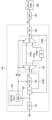
도 2를 참조하면, 디스플레이 구동 집적 회로(100)는 호스트 인터페이스(HIF)(151), 제어 로직(152), 인터페이스 모니터(MON), 라인 버퍼(LB)(153), 프로세싱 회로(PRC)(154), 경로 제어부(155), 프레임 버퍼(FB) 및 변환 회로(CON)(156)를 포함할 수 있다. Referring to FIG. 2, the display driver integrated circuit (100) may include a host interface (HIF) (151), control logic (152), an interface monitor (MON), a line buffer (LB) (153), a processing circuit (PRC) (154), a path control unit (155), a frame buffer (FB), and a conversion circuit (CON) (156).
도 2에는 데이터 드라이버(DDRV)(130) 및 디스플레이 패널(200)이 함께 도시되어 있다. 실시예에 따라서, 데이터 드라이버(130)는 디스플레이 구동 집적 회로(100)에 포함될 수 있다. FIG. 2 illustrates a data driver (DDRV) (130) and a display panel (200) together. Depending on the embodiment, the data driver (130) may be included in the display driver integrated circuit (100).
도 2에는 본 발명의 실시예들을 설명하기 위한 구성요소들만을 도시하였으며, 도 13을 참조하여 후술하는 바와 같이, 디스플레이 구동 집적 회로(100)는 스캔 드라이버, 전원 공급부, 감마 회로와 같은 구성 요소들을 더 포함할 수 있다. FIG. 2 illustrates only components for explaining embodiments of the present invention, and as described below with reference to FIG. 13, the display driving integrated circuit (100) may further include components such as a scan driver, a power supply, and a gamma circuit.
한편, 도 2에는 디스플레이 구동 집적 회로(100)가 프레임 버퍼(FB)를 포함하는 실시예를 도시하고 있으나, 후술하는 바와 같이, 실시예에 따라서 프레임 버퍼(FB)는 디스플레이 구동 집적 회로(100)의 외부에 구현될 수도 있다.Meanwhile, FIG. 2 illustrates an embodiment in which a display driver integrated circuit (100) includes a frame buffer (FB), but as described below, depending on the embodiment, the frame buffer (FB) may be implemented outside the display driver integrated circuit (100).
호스트 인터페이스(151)는 호스트 장치로부터 이미지 데이터(IMG)를 수신할 수 있다. 호스트 인터페이스(151)는 MIPI(Mobile Industry Processor Interface), DP(Display port), eDP(embedded DP) 등의 규격을 충족하도록 구현될 수 있다.The host interface (151) can receive image data (IMG) from the host device. The host interface (151) can be implemented to meet standards such as MIPI (Mobile Industry Processor Interface), DP (Display port), and eDP (embedded DP).
제어 로직(152)은 디스플레이 구동 집적 회로(100)에 포함되는 호스트 인터페이스(151), 인터페이스 모니터(MON), 라인 버퍼(153), 프로세싱 회로(154), 경로 제어부(155), 프레임 버퍼(FB) 및 변환 회로(156)의 전반적인 동작을 제어할 수 있다.The control logic (152) can control the overall operation of the host interface (151), interface monitor (MON), line buffer (153), processing circuit (154), path control unit (155), frame buffer (FB), and conversion circuit (156) included in the display driver integrated circuit (100).
인터페이스 모니터(MON)는 호스트 인터페이스(151)에 연결되고 상기 호스트 장치로부터 이미지 데이터(IMG)가 전송되는지 여부를 검출하여 정지영상 모드 또는 동영상 모드를 나타내는 모드 신호(MD)를 발생할 수 있다. 도 2에는 인터페이스 모니터(MON)가 제어 로직(152)에 포함되는 실시예를 도시하고 있으나, 실시예에 따라서 인터페이스 모니터(MON)는 제어 로직(152)과 구별되는 별개의 하드웨어로서 구현될 수 있다.The interface monitor (MON) is connected to the host interface (151) and can detect whether image data (IMG) is transmitted from the host device and generate a mode signal (MD) indicating a still image mode or a moving image mode. Fig. 2 illustrates an embodiment in which the interface monitor (MON) is included in the control logic (152), but depending on the embodiment, the interface monitor (MON) may be implemented as separate hardware distinct from the control logic (152).
디스플레이 분야에서 데이터 전송의 밴드 폭(band width)가 높아지면서 구동 칩, 보드 칩 시스템 간의 고속 데이터 전송이 요구되고 이에 따라 저전압 차동 신호(LVDS, Low voltage Differential Signaling) 방식이 널리 쓰이고 있다. LVDS 방식은 데이터 전송 속도를 증가하고 전력 소모를 감소하고 전자기 간섭(EMI, Electro-Magnetic Interference) 및 제조 비용을 감소할 수 있다. As the bandwidth of data transmission in the display field increases, high-speed data transmission between driver chips and board chip systems is required, and accordingly, low voltage differential signaling (LVDS) is widely used. LVDS can increase data transmission speed, reduce power consumption, and reduce electromagnetic interference (EMI) and manufacturing costs.
디스플레이 장치가 표시하는 이미지는 고 프레임율로 변하는 동영상과 일정 시간 고정되는 정지영상을 포함한다. 정지영상의 경우에는 전력 소모를 감소하기 위해 PSR(Panel Self Refresh) 방식을 채용하여 이미지 데이터를 전송하지 않을 수 있다. 그러나 이러한 PSR 방식은 LVDS 방식과 같은 단방향(uni-directional) 통신 방식에서는 동영상 데이터 및 정지영상 데이터를 모두 전송하여야 하므로 전력 소모의 감소를 도모하기가 곤란하다.Images displayed by display devices include moving images that change at high frame rates and still images that are fixed for a certain period of time. In the case of still images, the PSR (Panel Self Refresh) method can be adopted to reduce power consumption and not transmit image data. However, this PSR method is difficult to reduce power consumption because both moving image data and still image data must be transmitted in a unidirectional communication method such as the LVDS method.
본 발명의 실시예들에 따른 디스플레이 구동 집적 회로(100)는 인터페이스 모니터(MON)를 이용하여 동영상 모드 및 정지영상 모드를 결정함으로써 LVDS과 같은 단방향 통신에도 효율적으로 적용될 수 있다. 다시 말해, 본 발명의 실시예들에 따른 디스플레이 구동 집적 회로(100)는 동영상 모드에서 정지영상 모드로의 전환 및 정지영상 모드에서 동영상 모드로의 전환시 호스트 장치와의 동기화 과정을 필요로 하지 않는다.The display driver integrated circuit (100) according to embodiments of the present invention can be efficiently applied to unidirectional communication such as LVDS by determining the video mode and the still image mode using the interface monitor (MON). In other words, the display driver integrated circuit (100) according to embodiments of the present invention does not require a synchronization process with the host device when switching from the video mode to the still image mode and when switching from the still image mode to the video mode.
일 실시예에서, 도 3 등을 참조하여 후술하는 바와 같이, 인터페이스 모니터(MON)는 대기 시간 이내에 상기 호스트 인터페이스를 통하여 상기 호스트 장치로부터 상기 데이터 프레임이 전송되는지 여부를 모니터링하여 모드 신호(MD)를 발생할 수 있다. In one embodiment, as described below with reference to FIG. 3 and the like, an interface monitor (MON) may monitor whether the data frame is transmitted from the host device through the host interface within a waiting time and generate a mode signal (MD).
다른 실시예에서, 도 11을 참조하여 후술하는 바와 같이, 상기 호스트 장치가 이미지 데이터(IMG)의 현재 데이터 프레임이 정지영상 모드를 위한 것인지를 나타내는 모드 전환 정보를 디스플레이 구동 집적 회로(100)에 제공할 수 있고, 인터페이스 모니터(MON)는 상기 모드 전환 정보에 기초하여 모드 신호(MD)를 발생할 수 있다.In another embodiment, as described below with reference to FIG. 11, the host device may provide mode switching information indicating whether the current data frame of the image data (IMG) is for a still image mode to the display driver integrated circuit (100), and the interface monitor (MON) may generate a mode signal (MD) based on the mode switching information.
라인 버퍼(153)는 호스트 인터페이스(151) 및 프로세싱 회로(154) 사이에 배치되고 호스트 인터페이스(151)로부터의 이미지 데이터(IMG)를 라인 단위로 버퍼링하여 프로세싱 회로(154)로 출력할 수 있다.A line buffer (153) is arranged between the host interface (151) and the processing circuit (154) and can buffer image data (IMG) from the host interface (151) in line units and output it to the processing circuit (154).
프로세싱 회로(154)는 이미지 데이터(IMG)에 대한 프로세싱을 수행하여 프로세싱된 데이터(PDT)를 발생할 수 있다. 프로세싱 회로가 수행하는 이미치 처리 동작들에 대해서는 도 5를 참조하여 후술한다.The processing circuit (154) can perform processing on image data (IMG) to generate processed data (PDT). Image processing operations performed by the processing circuit will be described later with reference to FIG. 5.
경로 제어부(155)는 모드 신호(MD)에 기초하여 데이터의 전달 경로를 제어할 수 있다. 경로 제어부(155)는 모드 신호(MD)가 정지영상 모드를 나타내는 경우 프로세싱된 데이터(PDT)를 프레임 버퍼(BF)에 저장하고 프레임 버퍼(BF)에 저장된 프로세싱된 데이터(PDT)를 변환 회로(156)로 전달할 수 있다. 한편, 경로 제어부(155)는 모드 신호(MD)가 동영상 모드를 나타내는 경우 프레임 버퍼(BF)를 경유하지 않고 프로세싱된 데이터(PDT)를 변환 회로(156)로 전달할 수 있다.The path control unit (155) can control the transmission path of data based on the mode signal (MD). If the mode signal (MD) indicates a still image mode, the path control unit (155) can store processed data (PDT) in a frame buffer (BF) and transmit the processed data (PDT) stored in the frame buffer (BF) to the conversion circuit (156). Meanwhile, if the mode signal (MD) indicates a moving image mode, the path control unit (155) can transmit the processed data (PDT) to the conversion circuit (156) without going through the frame buffer (BF).
일 실시예에서, 경로 제어부(155)는 제1 경로 선택기(PS1) 및 제2 경로 선택기(PS2)를 포함할 수 있다.In one embodiment, the path control unit (155) may include a first path selector (PS1) and a second path selector (PS2).
제1 경로 선택기(PS1)는 모드 신호(MD)가 정지영상 모드를 나타내는 경우 프로세싱된 데이터(PDT)를 프레임 버퍼(FB)에 연결된 제1 경로(PTH1)로 출력할 수 있다. 한편, 제1 경로 선택기(PS1)는 모드 신호(MD)가 동영상 모드를 나타내는 경우 프로세싱된 데이터(PDT)를 프레임 버퍼(FB)에 연결되지 않은 제2 경로(PTH2)로 출력할 수 있다.The first path selector (PS1) can output the processed data (PDT) to the first path (PTH1) connected to the frame buffer (FB) when the mode signal (MD) indicates the still image mode. Meanwhile, the first path selector (PS1) can output the processed data (PDT) to the second path (PTH2) not connected to the frame buffer (FB) when the mode signal (MD) indicates the moving image mode.
제2 경로 선택기(PS2)는 모드 신호(MD)가 정지영상 모드를 나타내는 경우 프레임 버퍼(FB)에 연결된 제3 경로(PTH3)를 통하여 전달되는 프로세싱된 데이터(PDT)를 변환 회로(156)로 출력할 수 있다. 한편 제2 경로 선택기(PS2)는 모드 신호(MD)가 동영상 모드를 나타내는 경우 제2 경로(PTH2)를 통하여 전달되는 프로세싱된 데이터(PDT)를 변환 회로(156)로 출력할 수 있다. The second path selector (PS2) can output processed data (PDT) transmitted through the third path (PTH3) connected to the frame buffer (FB) to the conversion circuit (156) when the mode signal (MD) indicates a still image mode. Meanwhile, the second path selector (PS2) can output processed data (PDT) transmitted through the second path (PTH2) to the conversion circuit (156) when the mode signal (MD) indicates a moving image mode.
이와 같은 경로 제어부(155)를 이용하여 정지영상 모드에서는 프로세싱된 데이터(PDT)를 프레임 버퍼(BF)에 저장하고 프레임 버퍼(BF)에 저장된 프로세싱된 데이터(PDT)에 기초하여 디스플레이 데이터(DDT)를 발생하고, 동영상 모드에서는 프레임 버퍼(BF)를 경유하지 않은 프로세싱된 데이터(PDT)에 기초하여 디스플레이 데이터(DDT)를 발생할 수 있다.Using such a path control unit (155), in still image mode, processed data (PDT) can be stored in a frame buffer (BF) and display data (DDT) can be generated based on the processed data (PDT) stored in the frame buffer (BF), and in video mode, display data (DDT) can be generated based on processed data (PDT) that does not pass through the frame buffer (BF).
정지영상 모드에서는 프레임 버퍼(FR)에 저장된 프로세싱된 데이터(PDT)에 기초하여 디스플레이 데이터(DDT)를 발생하기 때문에 프로세싱 회로(154)는 모드 신호(MD)에 기초하여 상기 정지영상 모드에서 디스에이블될 수 있다. 또한, 정지영상 모드에서 상기 호스트 장치는 이미지 데이터(IMG)를 디스플레이 구동 집적 회로(100)로 전송할 필요가 없다. 이와 같이, 프로세싱 회로(154)의 디스에이블 및 호스트 장치로부터의 데이터 전송량의 감소를 통하여 디스플레이 구동 집적 회로(100) 및 디스플레이 구동 집적 회로(100)를 포함하는 디스플레이 장치의 전력 소모를 감소할 수 있다.In the still image mode, the processing circuit (154) can be disabled in the still image mode based on the mode signal (MD) because the display data (DDT) is generated based on the processed data (PDT) stored in the frame buffer (FR). In addition, in the still image mode, the host device does not need to transmit the image data (IMG) to the display driver integrated circuit (100). In this way, the power consumption of the display driver integrated circuit (100) and the display device including the display driver integrated circuit (100) can be reduced through the disabling of the processing circuit (154) and the reduction in the amount of data transmitted from the host device.
변환 회로(156)는 프로세싱된 데이터(PDT)에 대한 데이터 변환을 수행하여 디스플레이 패널(200)을 구동하기 위한 디스플레이 데이터(DDT)를 발생할 수 있다. 프로세싱 회로(156)는 동일한 입력에 대하여 동일한 출력을 제공하는 프로세싱을 수행할 수 있다. 반면에 변환 회로(156)는 입력에 대한 변경을 가하여 동일한 입력에 대해서 서로 다른 출력을 제공하는 데이터 변환을 수행할 수 있다. 일 실시예에서, 변환 회로(156)는 프로세싱된 데이터(PDT)에 대한 디더링(dithering)을 수행하여 디스플레이 데이터(DDT)를 발생할 수 있다. The conversion circuit (156) can perform data conversion on the processed data (PDT) to generate display data (DDT) for driving the display panel (200). The processing circuit (156) can perform processing that provides the same output for the same input. On the other hand, the conversion circuit (156) can perform data conversion that provides different outputs for the same input by changing the input. In one embodiment, the conversion circuit (156) can perform dithering on the processed data (PDT) to generate the display data (DDT).
이미지 처리에서의 디더링은 컴퓨터 프로그램이 주어진 색상을 표현하기 불가능할 때, 다른 색상들을 혼합한 근사 색상을 이용해 요구된 색상을 표현하고자 하는 방법을 말한다. 그림 기법 중 점묘법과 유사하게 두 개 이상의 다른 색상으로 점을 교차해서 배치시킴으로써 멀리서 보면 색이 혼합되어 보이게 하는 것이다. Dithering in image processing is a method of expressing a desired color using an approximate color mixed with other colors when a computer program cannot express a given color. Similar to pointillism in painting, it is a method of placing dots of two or more different colors in an alternating manner so that the colors appear to be mixed when viewed from a distance.
이미지 처리에서의 디더링 방법에는 평균(average) 디더링, 무작위(random) 디더링, 패턴(pattern) 디더링, 배열(ordered) 디더링 등이 있다. 예를 들어 고해상도 이미지를 낮은 해상도로 표현하는 경우, 자연스럽지 못하게 색이 이행되는 부분에 두 개 이상의 색을 섞어 찍음으로써 혼합된 색상을 표현하는 것이다.Dithering methods in image processing include average dithering, random dithering, pattern dithering, and ordered dithering. For example, when expressing a high-resolution image at a low resolution, two or more colors are mixed and printed in areas where the colors transition unnaturally to express mixed colors.
데이터 드라이버(DDRV)는 디스플레이 데이터(DDT)에 기초하여 이미지를 표시하도록 디스플레이 패널(200)을 구동할 수 있다. 데이터 드라이버(DDRV) 및 디스플레이 패널(200) 등을 포함하는 디스플레이 장치의 전체적인 구성 및 동작에 대해서는 도 12 및 13을 참조하여 후술한다.The data driver (DDRV) can drive the display panel (200) to display an image based on the display data (DDT). The overall configuration and operation of the display device including the data driver (DDRV) and the display panel (200) will be described later with reference to FIGS. 12 and 13.
이와 같이, 본 발명의 실시예들에 따른 디스플레이 구동 집적 회로는 데이터 검출기 및 경로 제어부를 이용하여 정지영상 디스플레이 모드 및 동영상 디스플레이 모드를 효율적으로 구현할 수 있다.In this way, the display driving integrated circuit according to embodiments of the present invention can efficiently implement a still image display mode and a moving image display mode by using a data detector and a path controller.
도 3은 본 발명의 실시예들에 따른 디스플레이 구동 집적 회로의 모드 신호의 발생에 관한 일 실시예를 나타내는 타이밍도이다.FIG. 3 is a timing diagram showing one embodiment of generation of a mode signal of a display driving integrated circuit according to embodiments of the present invention.
도 3을 참조하면, 호스트 장치는 코맨드(CMD) 및 이미지 데이터(IMG)를 디스플레이 구동 집적 회로로 전송할 수 있다. 도 3에는 코맨드(CMD) 및 이미지 데이터(IMG)를 별개의 신호들로 도시하였으나, 코맨드(CMD) 및 이미지 데이터(IMG)는 패킷의 형태로 통합되어 호스트 장치로부터 디스플레이 구동 집적 회로로 전송될 수 있다. 도 3에는 일 예로서 MIPI 표준의 write_memory_start (2Ch) 코맨드가 도시되어 있으나, 본 발명의 실시예들이 특정한 표준이나 코맨드에 한정되는 것은 아니다.Referring to FIG. 3, the host device can transmit a command (CMD) and image data (IMG) to the display driver integrated circuit. Although FIG. 3 illustrates the command (CMD) and the image data (IMG) as separate signals, the command (CMD) and the image data (IMG) can be integrated in the form of a packet and transmitted from the host device to the display driver integrated circuit. FIG. 3 illustrates the write_memory_start (2Ch) command of the MIPI standard as an example, but embodiments of the present invention are not limited to a specific standard or command.
호스트 장치는 수직 동기 신호(Vsync)에 동기하여 이미지 데이터(IMG)에 포함되는 데이터 프레임들(F(i))(여기서, i는 정수로서 데이터 프레임의 인덱스를 나타냄)을 디스플레이 구동 집적 회로로 전송할 수 있다. 도 3에는 수직 동기 신호(Vsync)의 활성화 시점들(T1~T3, T6~T10)에 동기하여 이미지 데이터(IMG)의 데이터 프레임들(F(N-3)~F(N+4)이 각각 전송되는 예가 도시되어 있다.A host device can transmit data frames (F(i)) (where i is an integer and represents an index of a data frame) included in image data (IMG) to a display driver integrated circuit in synchronization with a vertical synchronization signal (Vsync). FIG. 3 illustrates an example in which data frames (F(N-3) to F(N+4) of image data (IMG) are transmitted in synchronization with activation points (T1 to T3, T6 to T10) of a vertical synchronization signal (Vsync).
도 2를 참조하여 전술한 바와 같이, 인터페이스 모니터(MON)는 호스트 인터페이스(151)에 연결되고 상기 호스트 장치로부터 이미지 데이터(IMG)가 전송되는지 여부를 검출하여 정지영상 모드 또는 동영상 모드를 나타내는 모드 신호(MD)를 발생할 수 있다. As described above with reference to FIG. 2, the interface monitor (MON) is connected to the host interface (151) and can detect whether image data (IMG) is transmitted from the host device and generate a mode signal (MD) indicating a still image mode or a moving image mode.
모드 신호(MD)는 1비트의 신호일 수 있으며 모드 신호(MD)의 로직 레벨에 따라서 정지영상 모드 또는 동영상 모드를 나타낼 수 있다. 예를 들어, 도 3에 도시된 바와 같이 모드 신호(MD)의 로직 로우 레벨은 동영상 모드를 나타내고 모드 신호(MD)의 로직 하이 레벨은 정지영상 모드를 나타낼 수 있으나 본 발명의 실시예들이 이에 한정되는 것은 아니다.The mode signal (MD) can be a 1-bit signal and can indicate a still image mode or a video mode depending on the logic level of the mode signal (MD). For example, as shown in FIG. 3, a logic low level of the mode signal (MD) can indicate a video mode and a logic high level of the mode signal (MD) can indicate a still image mode, but embodiments of the present invention are not limited thereto.
일 실시예에서, 도 3에 도시된 바와 같이, 인터페이스 모니터(MON)는 대기 시간(tSB) 이내에 호스트 인터페이스(151)를 통하여 상기 호스트 장치로부터 데이터 프레임(F(i))이 전송되는지 여부를 모니터링하여 모드 신호(MD)를 발생할 수 있다. 즉, 인터페이스 모니터(MON)는 동영상 모드의 마지막 데이터 프레임(F(N-1))의 전송이 완료된 시점(T4)부터 대기 시간(tSB)이 경과할 때까지 이미지 데이터(IMG)가 전송되지 않는 경우, 대기 시간(tSB)의 경과 시점(T5)에서 모드 신호(MD)를 로직 로우 레벨에서 로직 하이 레벨로 천이하여 정지영상 모드에서 동영상 모드로 전환할 수 있다.In one embodiment, as illustrated in FIG. 3, the interface monitor (MON) may monitor whether a data frame (F(i)) is transmitted from the host device through the host interface (151) within a waiting time (tSB) to generate a mode signal (MD). That is, if image data (IMG) is not transmitted until the waiting time (tSB) elapses from a time point (T4) at which transmission of the last data frame (F(N-1)) of the video mode is completed, the interface monitor (MON) may transition the mode signal (MD) from a logic low level to a logic high level at a time point (T5) at which the waiting time (tSB) elapses, thereby switching from a still image mode to a video mode.
이와 같이, 본 발명의 실시예들에 따른 디스플레이 구동 집적 회로는 인터페이스 모니터(MON)를 이용하여 이미지 데이터(IMG)의 전송을 모니터링함으로써 호스트 장치와의 동기화 과정 없이 효율적으로 정지영상 모드 및 동영상 모드 사이의 전환을 제어할 수 있다.In this way, the display driver integrated circuit according to embodiments of the present invention can efficiently control switching between still image mode and moving image mode without a synchronization process with the host device by monitoring the transmission of image data (IMG) using an interface monitor (MON).
도 4는 본 발명의 실시예들에 따른 디스플레이 구동 집적 회로를 나타내는 블록도이다. FIG. 4 is a block diagram showing a display driving integrated circuit according to embodiments of the present invention.
도 4를 참조하면, 디스플레이 구동 집적 회로(101)는 호스트 인터페이스(HIF)(151), 제어 로직(152), 인터페이스 모니터(MON), 라인 버퍼(LB)(153), 프로세싱 회로(PRC)(154), 경로 제어부(155), 프레임 버퍼(FB), 변환 회로(CON)(156), 인코더(ENC) 및 디코더(DEC)를 포함할 수 있다. 도 4의 디스플레이 구동 집적 회로(101)는 도 2의 디스플레이 구동 집적 회로(100)와 비교하여 인코더(ENC) 및 디코더(DEC)를 더 포함하는 것을 제외하고는 실질적으로 동일하므로 중복되는 설명을 생략한다.Referring to FIG. 4, the display driver integrated circuit (101) may include a host interface (HIF) (151), a control logic (152), an interface monitor (MON), a line buffer (LB) (153), a processing circuit (PRC) (154), a path control unit (155), a frame buffer (FB), a conversion circuit (CON) (156), an encoder (ENC), and a decoder (DEC). The display driver integrated circuit (101) of FIG. 4 is substantially the same as the display driver integrated circuit (100) of FIG. 2 except that it further includes an encoder (ENC) and a decoder (DEC), and therefore, a redundant description is omitted.
인코더(ENC)는 프로세싱 회로(154) 및 프레임 버퍼(FB) 사이에 배치되고 프로세싱 회로(154)로부터 수신되는 프로세싱된 데이터(PDT)를 압축하여 압축 데이터를 프레임 버퍼(FB)에 저장할 수 있다.The encoder (ENC) is arranged between the processing circuit (154) and the frame buffer (FB) and can compress processed data (PDT) received from the processing circuit (154) and store the compressed data in the frame buffer (FB).
디코더(DEC)는 프레임 버퍼(FB) 및 변환 회로(156) 사이에 배치되고 프레임 버퍼(FB)로부터 독출되는 상기 압축 데이터를 압축해제하여 프로세싱된 데이터(PDT)를 변환 회로(156)로 전달할 수 있다.A decoder (DEC) is positioned between a frame buffer (FB) and a conversion circuit (156) and can decompress the compressed data read from the frame buffer (FB) and transmit the processed data (PDT) to the conversion circuit (156).
도 2를 참조하여 전술한 바와 같이, 경로 제어부(155)는 프로세싱 회로(154), 프레임 버퍼(FB) 및 변환 회로(156) 사이의 데이터 전달 경로를 제어하기 위한 제1 경로 선택기(PS1) 및 제2 경로 선택기(PS2)를 포함할 수 있다. As described above with reference to FIG. 2, the path control unit (155) may include a first path selector (PS1) and a second path selector (PS2) for controlling a data transmission path between the processing circuit (154), the frame buffer (FB), and the conversion circuit (156).
제1 경로 선택기(PS1)는 모드 신호(MD)에 기초하여 프로세싱 회로(154)로부터 제공되는 프로세싱된 데이터(PDT)를 제1 경로(PTH1) 또는 제2 경로(PTH2)로 출력한다. 제2 경로 선택기(PS2)는 모드 신호(MD)에 기초하여 제2 경로(PTH2) 또는 제3 경로(PTH3)를 통하여 제공되는 프로세싱된 데이터(PDT)를 변환 회로(156)로 전달한다. 이 경우, 인코더(ENC)는 제1 경로(PTH1) 상에 배치되고 디코더(DEC)는 제3 경로(PTH3) 상에 배치될 수 있다.The first path selector (PS1) outputs processed data (PDT) provided from the processing circuit (154) to the first path (PTH1) or the second path (PTH2) based on the mode signal (MD). The second path selector (PS2) transfers the processed data (PDT) provided through the second path (PTH2) or the third path (PTH3) to the conversion circuit (156) based on the mode signal (MD). In this case, the encoder (ENC) may be arranged on the first path (PTH1) and the decoder (DEC) may be arranged on the third path (PTH3).
인코더(ENC) 및 디코더(DEC)를 이용하여 프레임 버퍼(FB)의 사이즈를 감소할 수 있으나, 인코더(ENC)의 압축률이 증가할수록 데이터의 손실이 증가한다. 도 5를 참조하여 후술하는 바와 같이 프로세싱 회로(154)는 서브 픽셀 렌더링(SPR, Sub Pixel Rendering)을 수행할 수 있고, 서브 픽셀 렌더링에 의해 프로세싱된 데이터(PDT)의 용량이 감소될 수 있다. 이와 같이 프레임 버퍼(FB)를 프로세싱 회로(154)의 후단에 배치하고 용량이 감소된 프로세싱된 데이터(PDT)를 압축함으로써, 동일한 압축률을 적용하는 경우 이미지 데이터(IMG) 자체를 압축하는 것보다 데이터 손실을 감소할 수 있다. The size of the frame buffer (FB) can be reduced by using an encoder (ENC) and a decoder (DEC), but as the compression ratio of the encoder (ENC) increases, data loss increases. As described below with reference to FIG. 5, the processing circuit (154) can perform sub-pixel rendering (SPR), and the capacity of the processed data (PDT) can be reduced by the sub-pixel rendering. By placing the frame buffer (FB) at the rear end of the processing circuit (154) and compressing the processed data (PDT) with the reduced capacity, data loss can be reduced compared to compressing the image data (IMG) itself when the same compression ratio is applied.
도 5는 본 발명의 실시예들에 따른 디스플레이 구동 집적 회로에 포함되는 프로세싱 회로의 일 실시예를 나타내는 블록도이다.FIG. 5 is a block diagram illustrating one embodiment of a processing circuit included in a display driver integrated circuit according to embodiments of the present invention.
도 5를 참조하면, 프로세싱 회로(154)는 DSC(display stream compression) 디코더(DSCDEC), 제1 프로세싱 유닛(PRCBK1), 서브 픽셀 렌더링 유닛(SPR) 및 제2 프로세싱 유닛(PRCBK2)을 포함할 수 있다.Referring to FIG. 5, the processing circuit (154) may include a display stream compression (DSC) decoder (DSCDEC), a first processing unit (PRCBK1), a sub-pixel rendering unit (SPR), and a second processing unit (PRCBK2).
디스플레이 구동 집적 회로는 DSC 디코더(DSCDEC)를 구비하여 호스트 장치가 압축된 형태의 이미지 데이터(IMG)를 전송하는 것을 지원할 수 있다. DSC 디코더(DSCDEC)는 압축된 형태의 이미지 데이터(IMG)를 압축해제하여 제공할 수 있다. 실시예들에 따라서, DSC 디코더(DSCDEC)는 생략될 수 있다.The display driver integrated circuit may include a DSC decoder (DSCDEC) to support a host device to transmit image data (IMG) in a compressed form. The DSC decoder (DSCDEC) may decompress and provide the image data (IMG) in a compressed form. According to embodiments, the DSC decoder (DSCDEC) may be omitted.
제1 프로세싱 유닛(PRCBK1), 서브 픽셀 렌더링 유닛(SPR) 및 제2 프로세싱 유닛(PRCBK2)은 전체적으로 하나의 파이프라인 회로를 형성할 수 있다. 예를 들어, 제1 프로세싱 유닛(PRCBK1)은 스케일링(scaling), AoD(Always on Display), mDNIe(mobile Digital Natural Image engine), 라운딩(rounding) 등을 수행할 수 있고, 제2 프로세싱 유닛(PRCBK2)은 ACL(Automatic Current Limit), BC(Brightness Control), IRC (IR drop compensation), POC(Pixel Optical Compensation) 등을 수행할 수 있다.The first processing unit (PRCBK1), the sub-pixel rendering unit (SPR), and the second processing unit (PRCBK2) may form a single pipeline circuit as a whole. For example, the first processing unit (PRCBK1) may perform scaling, AoD (Always on Display), mDNIe (mobile Digital Natural Image engine), rounding, etc., and the second processing unit (PRCBK2) may perform ACL (Automatic Current Limit), BC (Brightness Control), IRC (IR drop compensation), POC (Pixel Optical Compensation), etc.
서브 픽셀 렌더링 유닛(SPR)은 제1 프로세싱 유닛(PRCBK1)으로부터 출력되는 데이터의 픽셀 포맷을 변환할 수 있다. 예를 들어, 서브 픽셀 렌더링 유닛(SPR)은 이미지 데이터(IMG)의 RGB 포맷을 RG/BG 포맷으로 변환하여 RG/BG 포맷의 데이터를 제2 프로세싱 유닛(PRCBK2)으로 제공할 수 있다. The sub-pixel rendering unit (SPR) can convert the pixel format of data output from the first processing unit (PRCBK1). For example, the sub-pixel rendering unit (SPR) can convert the RGB format of image data (IMG) into the RG/BG format and provide data in the RG/BG format to the second processing unit (PRCBK2).
서브 픽셀 렌더링 유닛(SPR)은 2개의 RGB 클러스터들에 포함되는 6개의 컬러 픽셀들을 1개의 RG/BG 클러스터에 포함되는 4개의 컬러 픽셀들로 변환할 수 있다. 만약 각각의 컬러 픽셀이 8비트로 구현되는 경우 서브 픽셀 렌더링 유닛(SPR)은 8*6=48비트의 데이터를 8*4=32비트의 데이터로 변환함으로써 데이터 용량이 감소될 수 있다.The sub-pixel rendering unit (SPR) can convert six color pixels included in two RGB clusters into four color pixels included in one RG/BG cluster. If each color pixel is implemented with 8 bits, the sub-pixel rendering unit (SPR) can reduce data capacity by converting 8*6=48 bits of data into 8*4=32 bits of data.
프로세싱 회로(154)는 프로세싱 과정에서의 중간 데이터 등을 저장하기 위한 보상용 메모리를 필요로 한다. 프로세싱 회로(154)가 수행하는 이미지 처리 동작들이 다양화되면서 보상용 메모리의 용량이 증가하게 된다. 보상용 메모리를 디스플레이 구동 집적 회로에 내장하는 경우 디스플레이 구동 집적 회로의 사이즈가 증가하게 되고 디스플레이 장치를 포함하는 모바일 장치의 설계 마진이 감소하게 된다.The processing circuit (154) requires a compensation memory to store intermediate data, etc. during the processing process. As the image processing operations performed by the processing circuit (154) become more diverse, the capacity of the compensation memory increases. When the compensation memory is embedded in the display driver integrated circuit, the size of the display driver integrated circuit increases and the design margin of the mobile device including the display device decreases.
도 6, 7 및 8은 본 발명의 실시예들에 따른 디스플레이 구동 집적 회로의 동작을 위한 보상용 메모리 및 프레임 버퍼의 배치에 관한 실시예들을 나타내는 도면들이다.FIGS. 6, 7 and 8 are drawings showing embodiments of arrangement of compensation memory and frame buffer for operation of a display driver integrated circuit according to embodiments of the present invention.
도 6, 7 및 8의 디스플레이 구동 집적 회로들(102, 103, 104)은 도 4의 디스플레이 구동 집적 회로(101)와 실질적으로 동일하므로 중복되는 설명을 생략하고 보상용 메모리 및 프레임 버퍼의 배치에 대해서만 설명하기로 한다. 이하, 도 6, 7 및 8의 디스플레이 구동 집적 회로들(102, 103, 104)의 각각은 하나의 반도체 칩으로 구현되는 것으로 간주될 수 있다. 여기서 하나의 반도체 칩은 패키징되어 다른 구성요소들과 물리적으로 구별되는 구성요소를 나타내며, 반도체 칩은 패키지의 표면에 배치되는 패드, 솔더 볼 등의 컨택들을 통하여 외부 장치들과 교신할 수 있다.The display driver integrated circuits (102, 103, 104) of FIGS. 6, 7, and 8 are substantially the same as the display driver integrated circuit (101) of FIG. 4, so that redundant descriptions are omitted and only the arrangement of the compensation memory and the frame buffer will be described. Hereinafter, each of the display driver integrated circuits (102, 103, 104) of FIGS. 6, 7, and 8 may be considered to be implemented as one semiconductor chip. Here, one semiconductor chip represents a component that is packaged and physically distinct from other components, and the semiconductor chip can communicate with external devices through contacts such as pads and solder balls arranged on the surface of the package.
도 6을 참조하면, 프레임 버퍼(FB)는 디스플레이 구동 집적 회로(102)를 구성하는 하나의 반도체 칩에 내장될 수 있다. 한편, 디스플레이 구동 집적 회로(102)는 프로세싱 회로(154)와 연결된 메모리 인터페이스(MIF)를 더 포함할 수 있고, 메모리 인터페이스(MIF)를 통하여 반도체 칩, 즉 디스플레이 구동 집적 회로(102)의 외부에 배치되는 외부 메모리(EXMEM)와 이미지 데이터(IMG)에 대한 프로세싱을 위한 데이터를 교환할 수 있다. 즉 전술한 보상용 메모리는 디스플레이 구동 집적 회로(102) 외부에 배치될 수 있다.Referring to FIG. 6, the frame buffer (FB) may be built into a single semiconductor chip constituting the display driver integrated circuit (102). Meanwhile, the display driver integrated circuit (102) may further include a memory interface (MIF) connected to a processing circuit (154), and may exchange data for processing image data (IMG) with an external memory (EXMEM) disposed outside the semiconductor chip, i.e., the display driver integrated circuit (102), through the memory interface (MIF). That is, the aforementioned compensation memory may be disposed outside the display driver integrated circuit (102).
도 7을 참조하면, 보상용 메모리 및 프레임 버퍼(FB)는 모두 디스플레이 구동 집적 회로(103)의 외부에 배치될 수 있다. 디스플레이 구동 집적 회로(103)는 프로세싱 회로(154)와 연결된 제1 메모리 인터페이스(MIF1) 및 경로 제어부(155)와 연결된 제2 메모리 인터페이스(MIF2)를 더 포함할 수 있다. Referring to FIG. 7, both the compensation memory and the frame buffer (FB) may be placed outside the display driver integrated circuit (103). The display driver integrated circuit (103) may further include a first memory interface (MIF1) connected to the processing circuit (154) and a second memory interface (MIF2) connected to the path control unit (155).
디스플레이 구동 집적 회로(103)는 제1 메모리 인터페이스(MIF1)를 통하여 외부 메모리(EXMEM)에 포함되는 보상용 메모리에 이미지 데이터(IMG)에 대한 프로세싱을 위한 데이터를 저장할 수 있고, 제2 메모리 인터페이스(MIF2)를 통하여 프레임 버퍼(FB)에 프로세싱된 데이터(PDT)를 저장할 수 있다. The display driver integrated circuit (103) can store data for processing image data (IMG) in a compensation memory included in an external memory (EXMEM) through a first memory interface (MIF1), and can store processed data (PDT) in a frame buffer (FB) through a second memory interface (MIF2).
실시예에 따라서, 도 9, 10 11을 참조하여 후술하는 바와 같이, 디스플레이 구동 집적 회로(103)는 동영상 모드에서 제2 메모리 인터페이스(MIF2)를 통하여 이미지 데이터(IMG)를 프레임 버퍼(FB)에 저장할 수 있다.According to an embodiment, as described below with reference to FIGS. 9, 10 and 11, the display driver integrated circuit (103) can store image data (IMG) in a frame buffer (FB) through a second memory interface (MIF2) in a video mode.
도 8을 참조하면, 보상용 메모리 및 프레임 버퍼(FB)는 모두 디스플레이 구동 집적 회로(103)의 외부에 배치되는 하나의 외부 메모리(EXMEM)에 포함될 수 있다. 디스플레이 구동 집적 회로(104)는 프로세싱 회로(154) 및 경로 제어부(155)와 연결된 메모리 인터페이스(MIF)를 더 포함할 수 있고, 메모리 인터페이스(MIF)를 통하여 외부 메모리(EXMEM)와 프로세싱을 위한 데이터 및 프로세싱된 데이터(PDT)를 교환할 수 있다. Referring to FIG. 8, both the compensation memory and the frame buffer (FB) may be included in one external memory (EXMEM) placed outside the display driver integrated circuit (103). The display driver integrated circuit (104) may further include a memory interface (MIF) connected to a processing circuit (154) and a path control unit (155), and may exchange data for processing and processed data (PDT) with the external memory (EXMEM) through the memory interface (MIF).
이와 같이, 본 발명의 실시예들에 따른 디스플레이 구동 집적 회로 및 디스플레이 장치는 프레임 버퍼 및 보상용 메모리를 디스플레이 구동 집적 회로의 내부 또는 외부에 적절히 배치함으로써 디스플레이 장치의 설계 마진을 향상시킬 수 있다.In this way, the display driving integrated circuit and display device according to embodiments of the present invention can improve the design margin of the display device by appropriately arranging the frame buffer and compensation memory inside or outside the display driving integrated circuit.
도 9는 본 발명의 실시예들에 따른 디스플레이 구동 집적 회로를 나타내는 블록도이다.FIG. 9 is a block diagram showing a display driving integrated circuit according to embodiments of the present invention.
도 9를 참조하면, 디스플레이 구동 집적 회로(105)는 호스트 인터페이스(HIF)(151), 제어 로직(152), 인터페이스 모니터(MON), 라인 버퍼(LB)(153), 프로세싱 회로(PRC)(154), 경로 제어부(155), 프레임 버퍼(FB) 및 변환 회로(CON)(156)를 포함할 수 있다. Referring to FIG. 9, the display driver integrated circuit (105) may include a host interface (HIF) (151), a control logic (152), an interface monitor (MON), a line buffer (LB) (153), a processing circuit (PRC) (154), a path control unit (155), a frame buffer (FB), and a conversion circuit (CON) (156).
도 9에는 데이터 드라이버(DDRV)(130) 및 디스플레이 패널(200)이 함께 도시되어 있다. 실시예에 따라서, 데이터 드라이버(130)는 디스플레이 구동 집적 회로(105)에 포함될 수 있다. 도 9에는 본 발명의 실시예들을 설명하기 위한 구성요소들만을 도시하였으며, 도 13을 참조하여 후술하는 바와 같이, 디스플레이 구동 집적 회로(105)는 스캔 드라이버, 전원 공급부, 감마 회로와 같은 구성 요소들을 더 포함할 수 있다. 한편, 도 9에는 디스플레이 구동 집적 회로(105)가 프레임 버퍼(FB)를 포함하는 실시예를 도시하고 있으나, 도 7 및 8을 참조하여 전술한 바와 같이 프레임 버퍼(FB)는 디스플레이 구동 집적 회로(105)의 외부에 구현될 수도 있다.FIG. 9 illustrates a data driver (DDRV) (130) and a display panel (200) together. According to an embodiment, the data driver (130) may be included in the display driver integrated circuit (105). FIG. 9 illustrates only components for explaining embodiments of the present invention, and as described below with reference to FIG. 13, the display driver integrated circuit (105) may further include components such as a scan driver, a power supply, and a gamma circuit. Meanwhile, FIG. 9 illustrates an embodiment in which the display driver integrated circuit (105) includes a frame buffer (FB), but as described above with reference to FIGS. 7 and 8, the frame buffer (FB) may be implemented external to the display driver integrated circuit (105).
호스트 인터페이스(151)는 호스트 장치로부터 이미지 데이터(IMG)를 수신할 수 있다. 호스트 인터페이스(151)는 MIPI(Mobile Industry Processor Interface), DP(Display port), eDP(embedded DP) 등의 규격을 충족하도록 구현될 수 있다.The host interface (151) can receive image data (IMG) from the host device. The host interface (151) can be implemented to meet standards such as MIPI (Mobile Industry Processor Interface), DP (Display port), and eDP (embedded DP).
제어 로직(152)은 디스플레이 구동 집적 회로(105)에 포함되는 호스트 인터페이스(151), 인터페이스 모니터(MON), 라인 버퍼(153), 프로세싱 회로(154), 경로 제어부(155), 프레임 버퍼(FB) 및 변환 회로(156)의 전반적인 동작을 제어할 수 있다.The control logic (152) can control the overall operation of the host interface (151), interface monitor (MON), line buffer (153), processing circuit (154), path control unit (155), frame buffer (FB), and conversion circuit (156) included in the display driver integrated circuit (105).
인터페이스 모니터(MON)는 호스트 인터페이스(151)에 연결되고 상기 호스트 장치로부터 이미지 데이터(IMG)가 전송되는지 여부를 검출하여 정지영상 모드 또는 동영상 모드를 나타내는 모드 신호(MD)를 발생할 수 있다. 도 9에는 인터페이스 모니터(MON)가 제어 로직(152)에 포함되는 실시예를 도시하고 있으나, 실시예에 따라서 인터페이스 모니터(MON)는 제어 로직(152)과 구별되는 별개의 하드웨어로서 구현될 수 있다.The interface monitor (MON) is connected to the host interface (151) and can detect whether image data (IMG) is transmitted from the host device and generate a mode signal (MD) indicating a still image mode or a moving image mode. Fig. 9 illustrates an embodiment in which the interface monitor (MON) is included in the control logic (152), but depending on the embodiment, the interface monitor (MON) may be implemented as separate hardware distinct from the control logic (152).
본 발명의 실시예들에 따른 디스플레이 구동 집적 회로(105)는 인터페이스 모니터(MON)를 이용하여 동영상 모드 및 정지영상 모드를 결정함으로써 LVDS과 같은 단방향 통신에도 효율적으로 적용될 수 있다. 다시 말해, 본 발명의 실시예들에 따른 디스플레이 구동 집적 회로(105)는 동영상 모드에서 정지영상 모드로의 전환 및 정지영상 모드에서 동영상 모드로의 전환시 호스트 장치와의 동기화 과정을 필요로 하지 않는다.The display driver integrated circuit (105) according to embodiments of the present invention can be efficiently applied to unidirectional communication such as LVDS by determining the video mode and the still image mode using the interface monitor (MON). In other words, the display driver integrated circuit (105) according to embodiments of the present invention does not require a synchronization process with the host device when switching from the video mode to the still image mode and when switching from the still image mode to the video mode.
일 실시예에서, 도 3 등을 참조하여 전술한 바와 같이, 인터페이스 모니터(MON)는 대기 시간(tSB) 이내에 상기 호스트 인터페이스를 통하여 상기 호스트 장치로부터 상기 데이터 프레임이 전송되는지 여부를 모니터링하여 모드 신호(MD)를 발생할 수 있다. 또한, 도 10을 참조하여 후술하는 바와 같이, 인터페이스 모니터(MON)는 인터페이스 모니터(MON)는 상기 동영상 모드에서 상기 정지영상 모드로의 전환을 나타내는 모드 전환 신호(MC)를 더 발생할 수 있다. In one embodiment, as described above with reference to FIG. 3 and the like, the interface monitor (MON) may monitor whether the data frame is transmitted from the host device through the host interface within the waiting time (tSB) and generate a mode signal (MD). In addition, as described below with reference to FIG. 10, the interface monitor (MON) may further generate a mode change signal (MC) indicating a change from the video mode to the still image mode.
다른 실시예에서, 도 11을 참조하여 후술하는 바와 같이, 상기 호스트 장치가 이미지 데이터(IMG)의 현재 데이터 프레임이 정지영상 모드를 위한 것인지를 나타내는 모드 전환 정보를 디스플레이 구동 집적 회로(105)에 제공할 수 있고, 디스플레이 구동 집적 회로(105)는 상기 모드 전환 정보에 기초하여 모드 신호(MD) 및 모드 전환 신호(MC)를 발생할 수 있다.In another embodiment, as described below with reference to FIG. 11, the host device may provide mode switching information indicating whether a current data frame of image data (IMG) is for a still image mode to the display driver integrated circuit (105), and the display driver integrated circuit (105) may generate a mode signal (MD) and a mode switching signal (MC) based on the mode switching information.
라인 버퍼(153)는 호스트 인터페이스(151) 및 프로세싱 회로(154) 사이에 배치되고 호스트 인터페이스(151)로부터의 이미지 데이터(IMG)를 라인 단위로 버퍼링하여 프로세싱 회로(154)로 출력할 수 있다.A line buffer (153) is arranged between the host interface (151) and the processing circuit (154) and can buffer image data (IMG) from the host interface (151) in line units and output it to the processing circuit (154).
프로세싱 회로(154)는 이미지 데이터(IMG)에 대한 프로세싱을 수행하여 프로세싱된 데이터(PDT)를 발생할 수 있다. 프로세싱 회로가 수행하는 이미치 처리 동작들에 대해서는 도 5를 참조하여 전술한 바와 같다.The processing circuit (154) can perform processing on image data (IMG) to generate processed data (PDT). The image processing operations performed by the processing circuit are as described above with reference to FIG. 5.
경로 제어부(155)는 모드 신호(MD)에 기초하여 데이터의 전달 경로를 제어할 수 있다. 경로 제어부(155)는 모드 신호(MD)가 정지영상 모드를 나타내는 경우 프로세싱된 데이터(PDT)를 프레임 버퍼(BF)에 저장하고 프레임 버퍼(BF)에 저장된 프로세싱된 데이터(PDT)를 변환 회로(156)로 전달할 수 있다. 한편, 경로 제어부(155)는 모드 신호(MD)가 동영상 모드를 나타내는 경우 프레임 버퍼(BF)를 경유하지 않고 프로세싱된 데이터(PDT)를 변환 회로(156)로 전달할 수 있다.The path control unit (155) can control the transmission path of data based on the mode signal (MD). If the mode signal (MD) indicates a still image mode, the path control unit (155) can store processed data (PDT) in a frame buffer (BF) and transmit the processed data (PDT) stored in the frame buffer (BF) to the conversion circuit (156). Meanwhile, if the mode signal (MD) indicates a moving image mode, the path control unit (155) can transmit the processed data (PDT) to the conversion circuit (156) without going through the frame buffer (BF).
일 실시예에서, 경로 제어부(155)는 제1 경로 선택기(PS1) 및 제2 경로 선택기(PS2)를 포함할 수 있다.In one embodiment, the path control unit (155) may include a first path selector (PS1) and a second path selector (PS2).
제1 경로 선택기(PS1)는 모드 신호(MD)가 정지영상 모드를 나타내는 경우 프로세싱된 데이터(PDT)를 프레임 버퍼(FB)에 연결된 제1 경로(PTH1)로 출력할 수 있다. 한편, 제1 경로 선택기(PS1)는 모드 신호(MD)가 동영상 모드를 나타내는 경우 프로세싱된 데이터(PDT)를 프레임 버퍼(FB)에 연결되지 않은 제2 경로(PTH2)로 출력할 수 있다.The first path selector (PS1) can output the processed data (PDT) to the first path (PTH1) connected to the frame buffer (FB) when the mode signal (MD) indicates the still image mode. Meanwhile, the first path selector (PS1) can output the processed data (PDT) to the second path (PTH2) not connected to the frame buffer (FB) when the mode signal (MD) indicates the moving image mode.
제2 경로 선택기(PS2)는 모드 신호(MD)가 정지영상 모드를 나타내는 경우 프레임 버퍼(FB)에 연결된 제3 경로(PTH3)를 통하여 전달되는 프로세싱된 데이터(PDT)를 변환 회로(156)로 출력할 수 있다. 한편 제2 경로 선택기(PS2)는 모드 신호(MD)가 동영상 모드를 나타내는 경우 제2 경로(PTH2)를 통하여 전달되는 프로세싱된 데이터(PDT)를 변환 회로(156)로 출력할 수 있다. The second path selector (PS2) can output processed data (PDT) transmitted through the third path (PTH3) connected to the frame buffer (FB) to the conversion circuit (156) when the mode signal (MD) indicates a still image mode. Meanwhile, the second path selector (PS2) can output processed data (PDT) transmitted through the second path (PTH2) to the conversion circuit (156) when the mode signal (MD) indicates a moving image mode.
이와 같은 경로 제어부(155)를 이용하여 정지영상 모드에서는 프로세싱된 데이터(PDT)를 프레임 버퍼(BF)에 저장하고 프레임 버퍼(BF)에 저장된 프로세싱된 데이터(PDT)에 기초하여 디스플레이 데이터(DDT)를 발생하고, 동영상 모드에서는 프레임 버퍼(BF)를 경유하지 않은 프로세싱된 데이터(PDT)에 기초하여 디스플레이 데이터(DDT)를 발생할 수 있다.Using such a path control unit (155), in still image mode, processed data (PDT) can be stored in a frame buffer (BF) and display data (DDT) can be generated based on the processed data (PDT) stored in the frame buffer (BF), and in video mode, display data (DDT) can be generated based on processed data (PDT) that does not pass through the frame buffer (BF).
정지영상 모드에서는 프레임 버퍼(FR)에 저장된 프로세싱된 데이터(PDT)에 기초하여 디스플레이 데이터(DDT)를 발생하기 때문에 프로세싱 회로(154)는 모드 신호(MD)에 기초하여 상기 정지영상 모드에서 디스에이블될 수 있다. 또한, 정지영상 모드에서 상기 호스트 장치는 이미지 데이터(IMG)를 디스플레이 구동 집적 회로(105)로 전송할 필요가 없다. In the still image mode, the processing circuit (154) can be disabled based on the mode signal (MD) because the display data (DDT) is generated based on the processed data (PDT) stored in the frame buffer (FR). In addition, in the still image mode, the host device does not need to transmit the image data (IMG) to the display driver integrated circuit (105).
이와 같이, 프로세싱 회로(154)의 디스에이블 및 호스트 장치로부터의 데이터 전송량의 감소를 통하여 디스플레이 구동 집적 회로(105) 및 디스플레이 구동 집적 회로(105)를 포함하는 디스플레이 장치의 전력 소모를 감소할 수 있다.In this way, power consumption of the display driver integrated circuit (105) and the display device including the display driver integrated circuit (105) can be reduced by disabling the processing circuit (154) and reducing the amount of data transmitted from the host device.
한편, 인터페이스 모니터(MON)는 상기 동영상 모드에서 상기 정지영상 모드로의 전환을 나타내는 모드 전환 신호(MC)를 더 발생할 수 있다. Meanwhile, the interface monitor (MON) can further generate a mode change signal (MC) indicating a change from the video mode to the still image mode.
일 실시예에서, 도 10을 참조하여 후술하는 바와 같이, 인터페이스 모니터(MON)는 대기 시간(tSB) 이내에 호스트 인터페이스(151)를 통하여 상기 호스트 장치로부터 이미지 데이터(IMG)가 전송되지 않는 경우 상기 동영상 모드에서 상기 정지영상 모드로의 전환을 나타내는 모드 전환 신호(MC)를 발생할 수 있다.In one embodiment, as described below with reference to FIG. 10, the interface monitor (MON) may generate a mode change signal (MC) indicating a change from the video mode to the still image mode when no image data (IMG) is transmitted from the host device through the host interface (151) within a waiting time (tSB).
다른 실시예에서, 도 11을 참조하여 후술하는 바와 같이, 인터페이스 모니터(MON)는 이미지 데이터(IMG)에 포함되는 데이터 프레임이 상기 동영상 모드의 마지막 데이터 프레임인 것을 나타내는 모드 전환 정보를 상기 호스트 장치로부터 수신하고 상기 모드 전환 정보에 기초하여 상기 동영상 모드에서 상기 정지영상 모드로의 전환을 나타내는 모드 전환 신호(MC)를 발생할 수 있다.In another embodiment, as described below with reference to FIG. 11, the interface monitor (MON) may receive mode switching information from the host device indicating that a data frame included in the image data (IMG) is the last data frame of the video mode, and may generate a mode switching signal (MC) indicating a switching from the video mode to the still image mode based on the mode switching information.
경로 제어부(155)의 제1 경로 선택기(PS1)는 제4 경로(PTH4)를 통하여 라인 버퍼(LB)에 연결되고 제2 경로 선택기(PS2)는 제5 경로(PTH5)를 통하여 라인 버퍼(LB)에 연결될 수 있다. 제1 경로 선택기(PS1)는 모드 신호(MD) 및 모드 전환 신호(MC)에 기초하여 상기 동영상 모드에서 제4 경로(PTH4)를 통하여 전송되는 이미지 데이터(IMG)에 포함되는 데이터 프레임, 즉 프로세싱 회로(154)에 의해 프로세싱되지 않은 데이터 프레임을 프레임 버퍼(FB)에 저장할 수 있다. The first path selector (PS1) of the path control unit (155) may be connected to the line buffer (LB) via the fourth path (PTH4), and the second path selector (PS2) may be connected to the line buffer (LB) via the fifth path (PTH5). The first path selector (PS1) may store, in the frame buffer (FB), a data frame included in the image data (IMG) transmitted via the fourth path (PTH4) in the video mode, i.e., a data frame not processed by the processing circuit (154), based on the mode signal (MD) and the mode change signal (MC).
한편, 경로 제어부(155)의 제2 경로 선택기(PS2)는 모드 신호(MD) 및 모드 전환 신호(MC)에 기초하여 상기 동영상 모드에서 상기 정지영상 모드로 전환시 프레임 버퍼(FB)로부터 독출되는 프레임 데이터를 제5 경로(PTH5)를 통하여 프로세싱 회로(154)에 제공할 수 있다. Meanwhile, the second path selector (PS2) of the path control unit (155) can provide frame data read from the frame buffer (FB) to the processing circuit (154) through the fifth path (PTH5) when switching from the video mode to the still image mode based on the mode signal (MD) and the mode switching signal (MC).
이와 같은 동영상 모드에서 정지영상 모드로의 전환시의 동작에 대해서는 도 10 및 11을 참조하여 후술한다.The operation when switching from video mode to still image mode is described later with reference to FIGS. 10 and 11.
변환 회로(156)는 프로세싱된 데이터(PDT)에 대한 데이터 변환을 수행하여 디스플레이 패널(200)을 구동하기 위한 디스플레이 데이터(DDT)를 발생할 수 있다. 프로세싱 회로(156)는 동일한 입력에 대하여 동일한 출력을 제공하는 프로세싱을 수행할 수 있다. 반면에 변환 회로(156)는 입력에 대한 변경을 가하여 동일한 입력에 대해서 서로 다른 출력을 제공하는 데이터 변환을 수행할 수 있다. 일 실시예에서, 변환 회로(156)는 프로세싱된 데이터(PDT)에 대한 디더링(dithering)을 수행하여 디스플레이 데이터(DDT)를 발생할 수 있다. The conversion circuit (156) can perform data conversion on the processed data (PDT) to generate display data (DDT) for driving the display panel (200). The processing circuit (156) can perform processing that provides the same output for the same input. On the other hand, the conversion circuit (156) can perform data conversion that provides different outputs for the same input by changing the input. In one embodiment, the conversion circuit (156) can perform dithering on the processed data (PDT) to generate the display data (DDT).
데이터 드라이버(DDRV)는 디스플레이 데이터(DDT)에 기초하여 이미지를 표시하도록 디스플레이 패널(200)을 구동할 수 있다. 데이터 드라이버(DDRV) 및 디스플레이 패널(200) 등을 포함하는 디스플레이 장치의 전체적인 구성 및 동작에 대해서는 도 12 및 13을 참조하여 후술한다.The data driver (DDRV) can drive the display panel (200) to display an image based on the display data (DDT). The overall configuration and operation of the display device including the data driver (DDRV) and the display panel (200) will be described later with reference to FIGS. 12 and 13.
이와 같이, 본 발명의 실시예들에 따른 디스플레이 구동 집적 회로는 데이터 검출기 및 경로 제어부를 이용하여 정지영상 디스플레이 모드 및 동영상 디스플레이 모드를 효율적으로 구현할 수 있다.In this way, the display driving integrated circuit according to embodiments of the present invention can efficiently implement a still image display mode and a moving image display mode by using a data detector and a path controller.
도 10 및 11은 도 9의 디스플레이 구동 집적 회로의 동작 방법의 실시예들을 나타내는 타이밍도들이다. 이하 도 3의 설명과 중복되는 설명은 생략될 수 있다.Figures 10 and 11 are timing diagrams showing embodiments of an operating method of the display driving integrated circuit of Figure 9. Any description that overlaps with the description of Figure 3 may be omitted.
도 10 및 11을 참조하면, 호스트 장치는 코맨드(CMD) 및 이미지 데이터(IMG)를 디스플레이 구동 집적 회로로 전송할 수 있다. 도 10 및 11에는 코맨드(CMD) 및 이미지 데이터(IMG)를 별개의 신호들로 도시하였으나, 코맨드(CMD) 및 이미지 데이터(IMG)는 패킷의 형태로 통합되어 호스트 장치로부터 디스플레이 구동 집적 회로로 전송될 수 있다. 도 10 및 11에는 일 예로서 MIPI 표준의 write_memory_start (2Ch) 코맨드가 도시되어 있으나, 본 발명의 실시예들이 특정한 표준이나 코맨드에 한정되는 것은 아니다.Referring to FIGS. 10 and 11, a host device can transmit a command (CMD) and image data (IMG) to a display driver integrated circuit. Although FIGS. 10 and 11 illustrate the command (CMD) and the image data (IMG) as separate signals, the command (CMD) and the image data (IMG) may be integrated in the form of a packet and transmitted from the host device to the display driver integrated circuit. FIGS. 10 and 11 illustrate the write_memory_start (2Ch) command of the MIPI standard as an example, but embodiments of the present invention are not limited to a specific standard or command.
호스트 장치는 수직 동기 신호(Vsync)에 동기하여 이미지 데이터(IMG)에 포함되는 데이터 프레임들(F(i))(여기서, i는 정수로서 데이터 프레임의 인덱스를 나타냄)을 디스플레이 구동 집적 회로로 전송할 수 있다. 도 10 및 11에는 수직 동기 신호(Vsync)의 활성화 시점들(T1~T5)에 동기하여 이미지 데이터(IMG)의 데이터 프레임들(F(N)~F(N+4)이 각각 전송되는 예가 도시되어 있다. 도 10 및 11에는 프레임 버퍼(FB)에 저장되는 데이터 프레임들이 함께 도시되어 있다. F(i)는 프로세싱 회로(154)에 의해 프로세싱되지 않은 본래의 데이터 프레임을 나타내고, PF(i)는 프로세싱된 데이터 프레임을 나타낸다.A host device can transmit data frames (F(i)) (where, i is an integer and represents an index of a data frame) included in image data (IMG) to a display driver integrated circuit in synchronization with a vertical synchronization signal (Vsync). FIGS. 10 and 11 illustrate examples in which data frames (F(N) to F(N+4)) of image data (IMG) are transmitted in synchronization with activation times (T1 to T5) of the vertical synchronization signal (Vsync), respectively. FIGS. 10 and 11 illustrate data frames stored in a frame buffer (FB) together. F(i) represents an original data frame that is not processed by a processing circuit (154), and PF(i) represents a processed data frame.
도 9를 참조하여 전술한 바와 같이, 인터페이스 모니터(MON)는 호스트 인터페이스(151)에 연결되고 상기 호스트 장치로부터 이미지 데이터(IMG)가 전송되는지 여부를 검출하여 정지영상 모드 또는 동영상 모드를 나타내는 모드 신호(MD)를 발생할 수 있다. 또한, 인터페이스 모니터(MON)는 상기 동영상 모드에서 상기 정지영상 모드로의 전환을 나타내는 모드 전환 신호(MC)를 발생할 수 있다. As described above with reference to FIG. 9, the interface monitor (MON) is connected to the host interface (151) and can detect whether image data (IMG) is transmitted from the host device and generate a mode signal (MD) indicating a still image mode or a moving image mode. In addition, the interface monitor (MON) can generate a mode change signal (MC) indicating a change from the moving image mode to the still image mode.
도 10은 이미지 데이터(IMG)에 포함되는 데이터 프레임이 동영상 모드의 마지막 데이터 프레임인 것을 나타내는 모드 전환 정보가 호스트 장치로부터 제공되지 않는 경우의 실시예를 나타낸다.FIG. 10 illustrates an embodiment in which mode switching information indicating that a data frame included in image data (IMG) is the last data frame of a video mode is not provided from the host device.
도 9 및 10을 참조하면, T1 시점까지는 프레임 버퍼(FB)에 저장된 프로세싱된 데이터 프레임(PF(N-1))에 기초하여 정지영상 모드가 수행될 수 있다. Referring to FIGS. 9 and 10, up to time T1, a still image mode can be performed based on a processed data frame (PF(N-1)) stored in a frame buffer (FB).
이후, T1~T5 시점들에서 호스트 장치로부터 정해진 프레임 레이트에 따라서 데이터 프레임들(F(N)~F(N+4))이 호스트 인터페이스(151)를 통하여 순차적으로 디스플레이 구동 집적 회로(105)로 전송될 수 있다. 이때, 동영상 모드를 나타내는 모드 신호(MD)에 기초하여 프로세싱 회로(154)에 의해 프로세싱되지 않은 데이터 프레임들(F(N)~F(N+4))이 제4 경로(PTH4), 제1 경로 선택기(PS1) 및 제1 경로(PTH1)를 통하여 프레임 버퍼(FB)에 순차적으로 저장될 수 있다. Thereafter, data frames (F(N) to F(N+4)) may be sequentially transmitted to the display driving integrated circuit (105) through the host interface (151) according to a frame rate determined from the host device at points in time T1 to T5. At this time, data frames (F(N) to F(N+4)) that are not processed by the processing circuit (154) based on a mode signal (MD) indicating a video mode may be sequentially stored in the frame buffer (FB) through the fourth path (PTH4), the first path selector (PS1), and the first path (PTH1).
결과적으로 동영상 모드에서, 제2 경로(PTH2)가 활성화되어 프로세싱된 데이터 프레임들이 프레임 버퍼(FB)를 거치지 않고 변환 회로(156)로 전달되는 동시에 제4 경로(PTH4) 및 제1 경로(PTH1)가 활성화되어 프로세싱되지 않은 마지막 데이터 프레임(F(N+4)이 프레임 버퍼(FB)에 저장될 수 있다. 동영상 모드에서 제3 경로(PTH3) 및 제5 경로(PTH5)는 비활성화될 수 있다.As a result, in the video mode, the second path (PTH2) is activated so that the processed data frames can be transmitted to the conversion circuit (156) without going through the frame buffer (FB), while the fourth path (PTH4) and the first path (PTH1) are activated so that the last unprocessed data frame (F(N+4)) can be stored in the frame buffer (FB). In the video mode, the third path (PTH3) and the fifth path (PTH5) can be deactivated.
인터페이스 모니터(MON)는 대기 시간(tSB) 이내에 호스트 인터페이스(151)를 통하여 상기 호스트 장치로부터 데이터 프레임(F(i))이 전송되는지 여부를 모니터링하여 모드 신호(MD) 및 모드 전환 신호(MC)를 발생할 수 있다. The interface monitor (MON) can monitor whether a data frame (F(i)) is transmitted from the host device through the host interface (151) within a waiting time (tSB) and generate a mode signal (MD) and a mode change signal (MC).
즉, 인터페이스 모니터(MON)는 동영상 모드의 마지막 데이터 프레임(F(N+4))의 전송이 완료된 시점(T6)부터 대기 시간(tSB)이 경과할 때까지 이미지 데이터(IMG)가 전송되지 않는 경우, 대기 시간(tSB)의 경과 시점(T7)에서 모드 신호(MD)를 로직 로우 레벨에서 로직 하이 레벨로 천이하여 정지영상 모드에서 동영상 모드로 전환할 수 있다. 또한, 인터페이스 모니터(MON)는 대기 시간(tSB)의 경과 시점(T7)에서 모드 전환 신호(MC)를 로직 로우 레벨에서 로직 하이 레벨로 천이할 수 있다.That is, if image data (IMG) is not transmitted until the waiting time (tSB) has elapsed from the time point (T6) when the transmission of the last data frame (F(N+4)) of the video mode is completed, the interface monitor (MON) can switch from the still image mode to the video mode by transitioning the mode signal (MD) from a logic low level to a logic high level at the time point (T7) when the waiting time (tSB) has elapsed. In addition, the interface monitor (MON) can transition the mode change signal (MC) from a logic low level to a logic high level at the time point (T7) when the waiting time (tSB) has elapsed.
경로 제어부(155)의 제2 경로 선택기(PS2)는 T7 시점에서 모드 전환 신호(MC)의 활성화에 응답하여 프레임 버퍼(FB)에 저장된 마지막 데이터 프레임(F(N+4))을 제5 경로(PTH5)를 통하여 프로세싱 회로(154)로 피드백할 수 있다. 피드백된 마지막 데이터 프레임(F(N+4)은 프로세싱 회로(154)에 의해 프로세싱되어 프로세싱된 마지막 데이터 프레임(PF(N+4)이 프레임 버퍼(FB)에 오버라이팅될 수 있다. 이후 T8~T10 시점들에서 프레임 버퍼(FB)에 저장된 프로세싱된 마지막 데이터 프레임(PF(N+4)에 기초하여 정지영상 모드가 수행될 수 있다.The second path selector (PS2) of the path control unit (155) can feed back the last data frame (F(N+4)) stored in the frame buffer (FB) to the processing circuit (154) through the fifth path (PTH5) in response to the activation of the mode switching signal (MC) at time point T7. The fed-back last data frame (F(N+4)) can be processed by the processing circuit (154), and the processed last data frame (PF(N+4)) can be overwritten in the frame buffer (FB). Thereafter, at time points T8 to T10, the still image mode can be performed based on the processed last data frame (PF(N+4)) stored in the frame buffer (FB).
도 11은 이미지 데이터(IMG)에 포함되는 데이터 프레임이 동영상 모드의 마지막 데이터 프레임인 것을 나타내는 모드 전환 정보(LFR)가 호스트 장치로부터 제공되는 경우의 실시예를 나타낸다. FIG. 11 illustrates an embodiment in which mode transition information (LFR) indicating that a data frame included in image data (IMG) is the last data frame of a video mode is provided from a host device.
도 11에는 모드 전환 정보(LFR)가 동영상 모드의 마지막 데이터 프레임(F(N+4))의 코맨드(CMD)에 포함되는 실시예를 도시하고 있다. 모드 전환 정보(LFR)는 코맨드(CMD)의 하나 이상의 비트들을 통하여 전달될 수 있다. 실시예에 따라서, 모드 전환 정보(LFR)는 별개의 제어 신호 라인을 통하여 호스트 장치로부터 디스플레이 구동 집적 회로(105)로 제공될 수도 있다.FIG. 11 illustrates an embodiment in which mode switching information (LFR) is included in the command (CMD) of the last data frame (F(N+4)) of the video mode. The mode switching information (LFR) may be transmitted via one or more bits of the command (CMD). According to an embodiment, the mode switching information (LFR) may also be provided from the host device to the display driver integrated circuit (105) via a separate control signal line.
도 9 및 11을 참조하면, T1 시점까지는 프레임 버퍼(FB)에 저장된 프로세싱된 데이터 프레임(PF(N-1))에 기초하여 정지영상 모드가 수행될 수 있다. Referring to FIGS. 9 and 11, up to time T1, a still image mode can be performed based on a processed data frame (PF(N-1)) stored in a frame buffer (FB).
이후, T1~T4 시점들에서 호스트 장치로부터 정해진 프레임 레이트에 따라서 데이터 프레임들(F(N)~F(N+3))이 호스트 인터페이스(151)를 통하여 순차적으로 디스플레이 구동 집적 회로(105)로 전송될 수 있다. Thereafter, data frames (F(N) to F(N+3)) can be sequentially transmitted to the display driving integrated circuit (105) through the host interface (151) according to a frame rate determined from the host device at points T1 to T4.
결과적으로 동영상 모드에서, 제2 경로(PTH2)가 활성화되어 프로세싱된 데이터 프레임들이 프레임 버퍼(FB)를 거치지 않고 변환 회로(156)로 전달하기 위해 제2 경로(PTH2)만이 활성화되고, 제1 경로(PTH1), 제3 경로(PTH3), 제4 경로(PTH4) 및 제5 경로(PTH5)는 비활성화될 수 있다.As a result, in the video mode, only the second path (PTH2) is activated so that the processed data frames can be transmitted to the conversion circuit (156) without going through the frame buffer (FB), and the first path (PTH1), the third path (PTH3), the fourth path (PTH4), and the fifth path (PTH5) can be deactivated.
인터페이스 모니터(MON)는 동영상 모드의 마지막 데이터 프레임(F(N+4))인 것을 나타내는 모드 전환 정보(LFR)에 기초하여 T5 시점에서 모드 신호(MD)를 로직 로우 레벨에서 로직 하이 레벨로 천이하여 정지영상 모드에서 동영상 모드로 전환할 수 있다. 또한, 인터페이스 모니터(MON)는 T5 시점에서 모드 전환 신호(MC)를 로직 로우 레벨에서 로직 하이 레벨로 천이할 수 있다.The interface monitor (MON) can switch from still image mode to video mode by transitioning the mode signal (MD) from a logic low level to a logic high level at time T5 based on mode transition information (LFR) indicating that it is the last data frame (F(N+4)) of the video mode. In addition, the interface monitor (MON) can transition the mode transition signal (MC) from a logic low level to a logic high level at time T5.
경로 제어부(155)의 제1 경로 선택기(PS1)는 T5 시점에서 모드 전환 신호(MC) 및 모드 전환 신호(MC)의 활성화에 응답하여 프로세싱 회로(154)를 인에이블시켜서 동영상 모드의 마지막 데이터 프레임(F(N+4)을 프로세싱한 마지막 데이터 프레임(PF(N+4))를 프레임 버퍼(FB)에 저장할 수 있다. 즉, 동영상 모드의 마지막 데이터 프레임(F(N+4))은 정지영상 모드의 데이터 프레임으로서 이용될 수 있다. The first path selector (PS1) of the path control unit (155) enables the processing circuit (154) in response to the mode change signal (MC) and the activation of the mode change signal (MC) at time T5 to store the last data frame (PF(N+4)) processed in the last data frame (F(N+4)) of the video mode in the frame buffer (FB). That is, the last data frame (F(N+4)) of the video mode can be used as a data frame of the still image mode.
결과적으로, T5~T10 시점들에서 프레임 버퍼(FB)에 저장된 프로세싱된 마지막 데이터 프레임(PF(N+4)에 기초하여 정지영상 모드가 수행될 수 있다.As a result, the still image mode can be performed based on the last processed data frame (PF(N+4)) stored in the frame buffer (FB) at points T5 to T10.
도 12는 본 발명의 실시예들에 따른 디스플레이 시스템을 나타내는 블록도이다.FIG. 12 is a block diagram showing a display system according to embodiments of the present invention.
도 12의 디스플레이 시스템(10)은 이미지 표시 기능을 갖는 이동 전화기(mobile phone), 스마트폰(smartphone), 태블릿 PC(tablet personal computer), PDA(personal digital assistant), 웨어러블 전자 장치 또는 PMP(potable multimedia player) 등과 같은 이동 장치(mobile device), 소형 기기(handheld device) 또는 소형 컴퓨터(handheld computer) 등으로 구현될 수 있다. 또한, 디스플레이 시스템(10)은 TV, 노트북, 데스크탑 PC, 네비게이션 장치 등 다양한 전자 장치로 구현될 수 있다.The display system (10) of FIG. 12 may be implemented as a mobile device, a handheld device, or a handheld computer, such as a mobile phone, a smartphone, a tablet personal computer, a personal digital assistant (PDA), a wearable electronic device, or a potable multimedia player (PMP), having an image display function. In addition, the display system (10) may be implemented as various electronic devices, such as a TV, a laptop, a desktop PC, or a navigation device.
도 12를 참조하면, 디스플레이 시스템(10)은 호스트 장치(20) 및 디스플레이 장치(30)를 포함할 수 있다. 디스플레이 장치(30)는 디스플레이 패널(200), 디스플레이 구동 집적 회로(DDI)(100) 및 메모리 장치(EXMEM)를 포함할 수 있다.Referring to FIG. 12, the display system (10) may include a host device (20) and a display device (30). The display device (30) may include a display panel (200), a display driver integrated circuit (DDI) (100), and a memory device (EXMEM).
호스트 장치(20)는 디스플레이 시스템(10)의 전반적인 동작을 제어할 수 있다. 호스트 장치(20)는 애플리케이션 프로세서(application processor; AP), 베이스밴드 프로세서(baseband processor; BBP), 또는 마이크로프로세싱 유닛(microprocessing unit; MPU) 등으로 구현될 수 있다. The host device (20) can control the overall operation of the display system (10). The host device (20) can be implemented as an application processor (AP), a baseband processor (BBP), or a microprocessing unit (MPU).
호스트 장치(20)는 이미지 데이터(IMG), 클록 신호(CLK) 및 디스플레이 장치(30)의 동작에 필요한 제어 신호들(CTRL)을 디스플레이 장치(30)로 전송할 수 있다. 예를 들어, 이미지 데이터(IMG)는 입력 영상에 관한 데이터이고, 복수의 RGB 픽셀 값을 포함할 수 있으며, 너비는 w개의 픽셀 값들을 갖고 높이는 h개의 픽셀 값들을 갖는 w*h의 해상도를 갖는 데이터일 수 있다. The host device (20) can transmit image data (IMG), a clock signal (CLK), and control signals (CTRL) required for the operation of the display device (30) to the display device (30). For example, the image data (IMG) is data regarding an input image, can include a plurality of RGB pixel values, and can be data having a resolution of w*h having w pixel values in width and h pixel values in height.
제어 신호들(CTRL)은 커맨드 신호, 수평 동기 신호, 수직 동기 신호, 데이터 인에이블 신호 등을 포함할 수 있다. 일 예로서, 이미지 데이터 및 제어 신호들은 패킷 데이터로서 디스플레이 구동 집적 회로(100)로 제공될 수 있다.The control signals (CTRL) may include a command signal, a horizontal sync signal, a vertical sync signal, a data enable signal, etc. As an example, the image data and the control signals may be provided to the display driver integrated circuit (100) as packet data.
커맨드 신호는 디스플레이 구동 집적 회로(100)가 수행하는 영상 처리를 제어하는 신호, 이미지 정보 또는 디스플레이 환경 설정 정보를 포함할 수 있다. The command signal may include a signal controlling image processing performed by the display driver integrated circuit (100), image information, or display environment setting information.
상기 이미지 정보는 디스플레이 구동 집적 회로(100)로 입력되는 이미지 데이터(IMG)에 관한 정보로서, 예를 들어 이미지 데이터(IMG)의 해상도 등을 포함할 수 있다. The above image information is information about image data (IMG) input to the display driving integrated circuit (100), and may include, for example, the resolution of the image data (IMG).
상기 디스플레이 환경 설정 정보는, 예를 들어, 패널 정보, 휘도 설정 값 등을 포함할 수 있다. 예를 들어, 호스트 장치(20)는 디스플레이 패널(200)의 사용자 입력에 따른 디스플레이 환경 설정 정보 또는 기설정된 디스플레이 환경 설정 정보를 디스플레이 구동 집적 회로(100)로 전송할 수 있다.The above display environment setting information may include, for example, panel information, brightness setting values, etc. For example, the host device (20) may transmit display environment setting information or preset display environment setting information according to user input of the display panel (200) to the display driver integrated circuit (100).
디스플레이 구동 집적 회로(100)는 호스트 장치(20)로부터 수신되는 이미지 데이터(IMG) 및 제어 신호들(CTRL)에 기초하여 디스플레이 패널(200)을 구동할 수 있다. 디스플레이 구동 집적 회로(100)는 디지털 신호인 이미지 데이터(IMG)를 아날로그 신호로 변환하고, 상기 아날로그 신호로 디스플레이 패널(200)을 구동할 수 있다. The display driving integrated circuit (100) can drive the display panel (200) based on image data (IMG) and control signals (CTRL) received from the host device (20). The display driving integrated circuit (100) can convert the image data (IMG), which is a digital signal, into an analog signal and drive the display panel (200) with the analog signal.
본 발명의 실시예들에 따라서, 디스플레이 구동 집적 회로(100)는 동작 모드를 제어하기 위한 인터페이스 모니터(MON) 및 경로 제어부(PCON)를 포함한다. According to embodiments of the present invention, a display driver integrated circuit (100) includes an interface monitor (MON) and a path control unit (PCON) for controlling an operation mode.
도 1 내지 11을 참조하여 전술한 바와 같이, 인터페이스 모니터(MON)는 호스트 인터페이스에 연결되고 호스트 장치(20)로부터 이미지 데이터(IMG)가 전송되는지 여부를 검출하여 정지영상 모드 또는 동영상 모드를 나타내는 모드 신호를 발생할 수 있다. 경로 제어부(PCON)는 상기 모드 신호에 기초하여, 상기 정지영상 모드에서 상기 프로세싱된 데이터를 프레임 버퍼에 저장하고 상기 프레임 버퍼에 저장된 상기 프로세싱된 데이터를 상기 변환 회로로 전달하고, 상기 동영상 모드에서 상기 프레임 버퍼를 경유하지 않고 상기 프로세싱된 데이터를 상기 변환 회로로 전달할 수 있다. 상기 프레임 버퍼는 디스플레이 구동 집적 회로(100) 내부에 포함될 수 있고, 디스플레이 구동 집적 회로(100) 외부에 배치되는 메모리 장치(EXMEM)에 포함될 수도 있다.As described above with reference to FIGS. 1 to 11, the interface monitor (MON) is connected to the host interface and can detect whether image data (IMG) is transmitted from the host device (20) and generate a mode signal indicating a still image mode or a moving image mode. Based on the mode signal, the path control unit (PCON) can store the processed data in a frame buffer in the still image mode and transfer the processed data stored in the frame buffer to the conversion circuit, and transfer the processed data to the conversion circuit without going through the frame buffer in the moving image mode. The frame buffer can be included in the display driver integrated circuit (100) or can be included in a memory device (EXMEM) disposed outside the display driver integrated circuit (100).
도 13은 본 발명의 실시예들에 따른 디스플레이 장치를 나타내는 블록도이다.FIG. 13 is a block diagram illustrating a display device according to embodiments of the present invention.
도 13을 참조하면, 전계발광 디스플레이 장치(30)는 복수의 픽셀 행들(211)을 포함하는 디스플레이 패널(200) 및 디스플레이 패널(200)을 구동하는 디스플레이 구동 집적 회로(100)를 포함한다. 디스플레이 구동 집적 회로(100)는 데이터 드라이버(130), 스캔 드라이버(140), 타이밍 컨트롤러(150), 전원 공급부(160) 및 감마 회로(170)를 포함할 수 있다.Referring to FIG. 13, an electroluminescent display device (30) includes a display panel (200) including a plurality of pixel rows (211) and a display driving integrated circuit (100) that drives the display panel (200). The display driving integrated circuit (100) may include a data driver (130), a scan driver (140), a timing controller (150), a power supply unit (160), and a gamma circuit (170).
디스플레이 패널(200)은 복수의 데이터 라인들을 통하여 디스플레이 구동 집적 회로(100)의 데이터 드라이버(130)와 연결되고, 복수의 스캔 라인들을 통하여 디스플레이 구동 집적 회로(100)의 스캔 드라이버(140)와 연결될 수 있다. 디스플레이 패널(200)은 복수의 화소(픽셀) 행들(211)을 포함할 수 있다. 디스플레이 패널(200)은 복수의 행들 및 복수의 열들을 가지는 매트릭스 형태로 배치된 복수의 화소들(PX)을 포함할 수 있고, 여기서, 하나의 화소 행(211)은 동일한 스캔 라인에 연결될 수 있는 하나의 행의 화소들(PX)을 의미한다. 일 실시예에서, 디스플레이 패널(200)은 백 라이트 없이 자체적으로 발광하는 자발광 디스플레이 패널일 수 있다. 예를 들어, 디스플레이 패널(200)은 OLED 패널일 수 있다.The display panel (200) may be connected to a data driver (130) of a display driving integrated circuit (100) through a plurality of data lines, and may be connected to a scan driver (140) of the display driving integrated circuit (100) through a plurality of scan lines. The display panel (200) may include a plurality of pixel rows (211). The display panel (200) may include a plurality of pixels (PX) arranged in a matrix form having a plurality of rows and a plurality of columns, wherein one pixel row (211) means one row of pixels (PX) that may be connected to the same scan line. In one embodiment, the display panel (200) may be a self-luminous display panel that emits light by itself without a backlight. For example, the display panel (200) may be an OLED panel.
일 실시예에서, 디스플레이 패널(200)에 포함된 각 화소(PX)는 구동 방식 등에 따른 다양한 구성을 가질 수 있다. 예를 들어, 상기 구동 방식은 계조를 표현하는 방식에 따라 아날로그 구동 또는 디지털 구동으로 구분될 수 있다. 아날로그 구동은 발광 다이오드(이하, 유기 발광 다이오드를 포함한다)가 동일한 발광 시간 동안 발광하면서 화소(또는 픽셀)에 인가되는 데이터 전압의 레벨을 변경함으로써 계조를 표현할 수 있다. 디지털 구동은 화소에 동일한 레벨의 데이터 전압을 인가하면서 발광 다이오드가 발광되는 발광 시간을 변경함으로써 계조를 표현할 수 있다. 이러한 디지털 구동은, 아날로그 구동에 비하여, 전계발광 디스플레이 장치가 간단한 구조의 화소 및 구동 IC(Integrated Circuit)를 포함하는 장점이 있다. 또한, 전계발광 디스플레이 장치의 디스플레이 패널이 대형화되고 해상도가 높아질수록 디지털 구동을 채택할 필요성이 증가된다. 본 발명의 실시예들에 따른 디스플레이 장치는 이러한 아날로그 구동 및 디지털 구동에 모두 적용될 수 있다.In one embodiment, each pixel (PX) included in the display panel (200) may have various configurations according to the driving method, etc. For example, the driving method may be classified into analog driving or digital driving depending on the method of expressing grayscale. Analog driving can express grayscale by changing the level of data voltage applied to a pixel (or pixel) while a light-emitting diode (hereinafter, including an organic light-emitting diode) emits light for the same light-emitting time. Digital driving can express grayscale by changing the light-emitting time during which a light-emitting diode emits light while applying the same level of data voltage to the pixel. Such digital driving has an advantage over analog driving in that an electroluminescent display device includes pixels and a driving IC (Integrated Circuit) with a simple structure. In addition, as the display panel of an electroluminescent display device becomes larger and the resolution increases, the need to adopt digital driving increases. Display devices according to embodiments of the present invention can be applied to both such analog driving and digital driving.
데이터 드라이버(130)는 상기 복수의 데이터 라인들을 통하여 디스플레이 패널(200)에 데이터 신호를 인가할 수 있고, 스캔 드라이버(140)는 상기 복수의 스캔 라인들을 통하여 디스플레이 패널(200)에 스캔 신호를 인가할 수 있다. The data driver (130) can apply a data signal to the display panel (200) through the plurality of data lines, and the scan driver (140) can apply a scan signal to the display panel (200) through the plurality of scan lines.
타이밍 컨트롤러(150)는 디스플레이 장치(30)의 동작을 제어할 수 있다. 타이밍 컨트롤러(150)는 소정의 제어 신호들을 데이터 드라이버(130) 및 스캔 드라이버(140)에 제공함으로써 디스플레이 장치(30)의 동작을 제어할 수 있다. 일 실시예에서, 데이터 드라이버(130), 스캔 드라이버(140) 및 타이밍 컨트롤러(150)는 하나의 집적 회로(Integrated Circuit; IC)로 구현될 수 있다. 다른 실시예에서, 데이터 드라이버(130), 스캔 드라이버(140) 및 타이밍 컨트롤러(150)는 2 이상의 IC들로 구현될 수 있다. 적어도 상기 타이밍 콘트롤러(150) 및 상기 데이터 드라이버(130)가 일체로 형성된 구동 모듈을 타이밍 컨트롤러 임베디드 데이터 드라이버(Timing Controller Embedded Data Driver, TED)로 명명할 수 있다.The timing controller (150) can control the operation of the display device (30). The timing controller (150) can control the operation of the display device (30) by providing predetermined control signals to the data driver (130) and the scan driver (140). In one embodiment, the data driver (130), the scan driver (140), and the timing controller (150) can be implemented as one integrated circuit (IC). In another embodiment, the data driver (130), the scan driver (140), and the timing controller (150) can be implemented as two or more ICs. A driving module in which at least the timing controller (150) and the data driver (130) are formed integrally can be named a timing controller embedded data driver (TED).
상기 타이밍 콘트롤러(150)는 호스트 장치, 예를 들어, 도 12의 호스트 장치(20)로부터 이미지 데이터(IMG) 및 입력 제어 신호들을 수신한다. 예를 들어, 상기 이미지 데이터(IMG)는 적색 영상 데이터(R), 녹색 영상 데이터(G) 및 청색 영상 데이터(B)를 포함할 수 있다. 상기 이미지 데이터(IMG)는 백색 영상 데이터를 포함할 수 있다. 상기 이미지 데이터(IMG)는 마젠타색(magenta) 영상 데이터, 황색(yellow) 영상 데이터 및 시안색(cyan) 영상 데이터를 포함할 수 있다.The timing controller (150) receives image data (IMG) and input control signals from a host device, for example, the host device (20) of FIG. 12. For example, the image data (IMG) may include red image data (R), green image data (G), and blue image data (B). The image data (IMG) may include white image data. The image data (IMG) may include magenta image data, yellow image data, and cyan image data.
상기 입력 제어 신호들은 마스터 클럭 신호, 데이터 인에이블 신호를 포함할 수 있다. 또한 상기 입력 제어 신호들은 수직 동기 신호 및 수평 동기 신호를 더 포함할 수 있다.The above input control signals may include a master clock signal, a data enable signal. In addition, the above input control signals may further include a vertical synchronization signal and a horizontal synchronization signal.
전원 공급부(160)는 디스플레이 패널(200)에 전원 전압(ELVDD) 및 접지 전압(ELVSS))을 공급할 수 있다. 실시예에 따라서, ELVDD는 고 전원 전압에 해당하고 ELVSS는 저 전원 전압에 해당할 수 있다. 또한, 전원 공급부(160)는 감마 회로(170)에 레귤레이터 전압(VREG)을 공급할 수 있다.The power supply unit (160) can supply a power voltage (ELVDD) and a ground voltage (ELVSS) to the display panel (200). According to an embodiment, ELVDD may correspond to a high power voltage and ELVSS may correspond to a low power voltage. In addition, the power supply unit (160) can supply a regulator voltage (VREG) to the gamma circuit (170).
감마 회로(170)는 레귤레이터 전압(VREG)에 기초하여 복수의 감마 기준 전압들(GRV)을 발생할 수 있다. 예를 들어, 레귤레이터 전압(VREG)은 전원 전압(ELVDD)일 수도 있고, 전원 전압(ELVDD)에 기초하여 별도의 레귤레이터 전압에 의해 발생되는 전압일 수도 있다.The gamma circuit (170) can generate a plurality of gamma reference voltages (GRV) based on the regulator voltage (VREG). For example, the regulator voltage (VREG) may be the power supply voltage (ELVDD) or may be a voltage generated by a separate regulator voltage based on the power supply voltage (ELVDD).
본 발명의 실시예들에 따라서, 타이밍 컨트롤러(150)는 디스플레이 구동 집적 회로(100)는 동작 모드를 제어하기 위한 인터페이스 모니터(MON) 및 경로 제어부(PCON)를 포함한다. According to embodiments of the present invention, the timing controller (150) includes an interface monitor (MON) and a path control unit (PCON) for controlling the operation mode of the display driving integrated circuit (100).
도 1 내지 11을 참조하여 전술한 바와 같이, 인터페이스 모니터(MON)는 호스트 인터페이스에 연결되고 호스트 장치(20)로부터 이미지 데이터(IMG)가 전송되는지 여부를 검출하여 정지영상 모드 또는 동영상 모드를 나타내는 모드 신호를 발생할 수 있다. 경로 제어부(PCON)는 상기 모드 신호에 기초하여, 상기 정지영상 모드에서 상기 프로세싱된 데이터를 프레임 버퍼에 저장하고 상기 프레임 버퍼에 저장된 상기 프로세싱된 데이터를 상기 변환 회로로 전달하고, 상기 동영상 모드에서 상기 프레임 버퍼를 경유하지 않고 상기 프로세싱된 데이터를 상기 변환 회로로 전달할 수 있다. 상기 프레임 버퍼는 디스플레이 구동 집적 회로(100) 내부에 포함될 수 있고, 디스플레이 구동 집적 회로(100) 외부에 배치되는 메모리 장치(EXMEM)에 포함될 수도 있다.As described above with reference to FIGS. 1 to 11, the interface monitor (MON) is connected to the host interface and can detect whether image data (IMG) is transmitted from the host device (20) and generate a mode signal indicating a still image mode or a moving image mode. Based on the mode signal, the path control unit (PCON) can store the processed data in a frame buffer in the still image mode and transfer the processed data stored in the frame buffer to the conversion circuit, and transfer the processed data to the conversion circuit without going through the frame buffer in the moving image mode. The frame buffer can be included in the display driver integrated circuit (100) or can be included in a memory device (EXMEM) disposed outside the display driver integrated circuit (100).
도 14는 본 발명의 실시예들에 따른 모바일 장치를 나타내는 블록도이다.FIG. 14 is a block diagram illustrating a mobile device according to embodiments of the present invention.
도 14를 참조하면, 모바일 장치(700)는 시스템 온 칩(710) 및 복수의 또는 기능 모듈들(740, 750, 760, 770)을 포함한다. 모바일 장치(700)는 메모리 장치(720), 저장 장치(730) 및 전력 관리 장치(780)를 더 포함할 수 있다. Referring to FIG. 14, a mobile device (700) includes a system on chip (710) and a plurality of or functional modules (740, 750, 760, 770). The mobile device (700) may further include a memory device (720), a storage device (730), and a power management device (780).
시스템 온 칩(710)은 모바일 장치(700)의 전반적인 동작을 제어할 수 있다. 다시 말하면, 시스템 온 칩(710)은 메모리 장치(720), 저장 장치(730) 및 복수의 기능 모듈들(740, 750, 760, 770)을 제어할 수 있다. 예를 들어, 시스템 온 칩(710)은 모바일 장치(700)에 구비되는 애플리케이션 프로세서(Application Processor; AP)일 수 있다.The system on chip (710) can control the overall operation of the mobile device (700). In other words, the system on chip (710) can control a memory device (720), a storage device (730), and a plurality of functional modules (740, 750, 760, 770). For example, the system on chip (710) can be an application processor (AP) equipped in the mobile device (700).
시스템 온 칩(710)은 중앙 처리 유닛(712) 및 전력 관리 시스템(714)을 포함할 수 있다. 메모리 장치(720) 및 저장 장치(730)는 모바일 장치(700)의 동작에 필요한 데이터들을 저장할 수 있다. 예를 들어, 메모리 장치(720)는 DRAM(dynamic random access memory) 장치, SRAM(static random access memory) 장치, 모바일 DRAM 장치 등과 같은 휘발성 메모리 장치에 상응할 수 있고, 저장 장치(730)는 EPROM(erasable programmable read-only memory) 장치, EEPROM(electrically erasable programmable read-only memory) 장치, 플래시 메모리(flash memory) 장치, PRAM(phase change random access memory) 장치, RRAM(resistance random access memory) 장치, NFGM(nano floating gate memory) 장치, PoRAM(polymer random access memory) 장치, MRAM(magnetic random access memory) 장치, FRAM(ferroelectric random access memory) 장치 등과 같은 비휘발성 메모리 장치에 상응할 수 있다. 실시예에 따라서, 저장 장치(730)는 솔리드 스테이트 드라이브(solid state drive; SSD), 하드 디스크 드라이브(hard disk drive; HDD), 씨디롬(CD-ROM) 등을 더 포함할 수도 있다.The system on chip (710) may include a central processing unit (712) and a power management system (714). The memory device (720) and the storage device (730) may store data required for the operation of the mobile device (700). For example, the memory device (720) may correspond to a volatile memory device such as a dynamic random access memory (DRAM) device, a static random access memory (SRAM) device, a mobile DRAM device, and the like, and the storage device (730) may correspond to a nonvolatile memory device such as an erasable programmable read-only memory (EPROM) device, an electrically erasable programmable read-only memory (EEPROM) device, a flash memory device, a phase change random access memory (PRAM) device, a resistance random access memory (RRAM) device, a nano floating gate memory (NFGM) device, a polymer random access memory (PoRAM) device, a magnetic random access memory (MRAM) device, a ferroelectric random access memory (FRAM) device, and the like. According to an embodiment, the storage device (730) may further include a solid state drive (SSD), a hard disk drive (HDD), a CD-ROM, and the like.
복수의 기능 모듈들(740, 750, 760, 770)은 모바일 장치(700)의 다양한 기능들을 각각 수행할 수 있다. 예를 들어, 모바일 장치(700)는 통신 기능을 수행하기 위한 통신 모듈(740)(예를 들어, CDMA(code division multiple access) 모듈, LTE(long term evolution) 모듈, RF(radio frequency) 모듈, UWB(ultra wideband) 모듈, WLAN(wireless local area network) 모듈, WIMAX(worldwide interoperability for microwave access) 모듈 등), 카메라 기능을 수행하기 위한 카메라 모듈(750), 표시 기능을 수행하기 위한 디스플레이 모듈(760), 터치 입력 기능을 수행하기 위한 터치 패널 모듈(770) 등을 포함할 수 있다. 실시예에 따라서, 모바일 장치(700)는 GPS(global positioning system) 모듈, 마이크 모듈, 스피커 모듈, 자이로스코프(gyroscope) 모듈 등을 더 포함할 수 있다. 다만, 모바일 장치(700)에 구비되는 복수의 기능 모듈들(740, 750, 760, 770)의 종류는 그에 한정되지 않음은 자명하다.The plurality of function modules (740, 750, 760, 770) may each perform various functions of the mobile device (700). For example, the mobile device (700) may include a communication module (740) for performing a communication function (e.g., a code division multiple access (CDMA) module, a long term evolution (LTE) module, a radio frequency (RF) module, an ultra wideband (UWB) module, a wireless local area network (WLAN) module, a worldwide interoperability for microwave access (WIMAX) module, etc.), a camera module (750) for performing a camera function, a display module (760) for performing a display function, a touch panel module (770) for performing a touch input function, etc. According to an embodiment, the mobile device (700) may further include a GPS (global positioning system) module, a microphone module, a speaker module, a gyroscope module, etc. However, it is obvious that the types of multiple function modules (740, 750, 760, 770) equipped in the mobile device (700) are not limited thereto.
전력 관리 장치(780)는 시스템 온 칩(710), 메모리 장치(720), 저장 장치(730) 및 복수의 기능 모듈들(740, 750, 760, 770)에 각각 구동 전압을 제공할 수 있다.The power management device (780) can provide driving voltage to each of the system on chip (710), the memory device (720), the storage device (730), and the plurality of functional modules (740, 750, 760, 770).
본 발명의 실시예들에 따라서, 디스플레이 모듈(760)은 전술한 바와 같은 인터페이스 모니터(MON) 및 경로 제어부(PCON)를 포함하는 디스플레이 구동 집적 회로(DDIC)(762)를 포함할 수 있다. 도 1 내지 11을 참조하여 전술한 바와 같이, 인터페이스 모니터(MON)는 호스트 인터페이스에 연결되고 호스트 장치로부터 이미지 데이터(IMG)가 전송되는지 여부를 검출하여 정지영상 모드 또는 동영상 모드를 나타내는 모드 신호를 발생할 수 있다. 경로 제어부(PCON)는 상기 모드 신호에 기초하여, 상기 정지영상 모드에서 상기 프로세싱된 데이터를 프레임 버퍼에 저장하고 상기 프레임 버퍼에 저장된 상기 프로세싱된 데이터를 상기 변환 회로로 전달하고, 상기 동영상 모드에서 상기 프레임 버퍼를 경유하지 않고 상기 프로세싱된 데이터를 상기 변환 회로로 전달할 수 있다.According to embodiments of the present invention, the display module (760) may include a display driver integrated circuit (DDIC) (762) including an interface monitor (MON) and a path controller (PCON) as described above. As described above with reference to FIGS. 1 to 11, the interface monitor (MON) may be connected to a host interface and may detect whether image data (IMG) is transmitted from a host device and generate a mode signal indicating a still image mode or a moving image mode. The path controller (PCON) may store the processed data in a frame buffer in the still image mode and transmit the processed data stored in the frame buffer to the conversion circuit based on the mode signal, and transmit the processed data to the conversion circuit without going through the frame buffer in the moving image mode.
도 15는 도 14의 모바일 장치에서 사용되는 인터페이스의 일 예를 나타내는 블록도이다.FIG. 15 is a block diagram showing an example of an interface used in the mobile device of FIG. 14.
도 15를 참조하면, 컴퓨팅 시스템(1100)은 MIPI 인터페이스를 사용 또는 지원할 수 있는 데이터 처리 장치로 구현될 수 있고, 어플리케이션 프로세서(1110), 이미지 센서(1140) 및 디스플레이(1150) 등을 포함할 수 있다. Referring to FIG. 15, a computing system (1100) may be implemented as a data processing device capable of using or supporting a MIPI interface, and may include an application processor (1110), an image sensor (1140), and a display (1150).
어플리케이션 프로세서(1110)의 CSI 호스트(1112)는 카메라 시리얼 인터페이스(Camera Serial Interface; CSI)를 통하여 이미지 센서(1140)의 CSI 장치(1141)와 시리얼 통신을 수행할 수 있다. The CSI host (1112) of the application processor (1110) can perform serial communication with the CSI device (1141) of the image sensor (1140) through a camera serial interface (CSI).
일 실시예에서, CSI 호스트(1112)는 디시리얼라이저(DES)를 포함할 수 있고, CSI 장치(1141)는 시리얼라이저(SER)를 포함할 수 있다. 어플리케이션 프로세서(1110)의 DSI 호스트(1111)는 디스플레이 시리얼 인터페이스(Display Serial Interface; DSI)를 통하여 디스플레이(1150)의 DSI 장치(1151)와 시리얼 통신을 수행할 수 있다. In one embodiment, the CSI host (1112) may include a deserializer (DES) and the CSI device (1141) may include a serializer (SER). The DSI host (1111) of the application processor (1110) may perform serial communication with the DSI device (1151) of the display (1150) via a display serial interface (DSI).
일 실시예에서, DSI 호스트(1111)는 시리얼라이저(SER)를 포함할 수 있고, DSI 장치(1151)는 디시리얼라이저(DES)를 포함할 수 있다. 나아가, 컴퓨팅 시스템(1100)은 어플리케이션 프로세서(1110)와 통신을 수행할 수 있는 알에프(Radio Frequency; RF) 칩(1160)을 더 포함할 수 있다. In one embodiment, the DSI host (1111) may include a serializer (SER) and the DSI device (1151) may include a deserializer (DES). Furthermore, the computing system (1100) may further include a Radio Frequency (RF) chip (1160) capable of communicating with the application processor (1110).
컴퓨팅 시스템(1100)의 PHY(1113)와 RF 칩(1160)의 PHY(1161)는 MIPI(Mobile Industry Processor Interface) DigRF에 따라 데이터 송수신을 수행할 수 있다. 또한, 어플리케이션 프로세서(1110)는 PHY(1161)의 MIPI DigRF에 따른 데이터 송수신을 제어하는 DigRF MASTER(1114)를 더 포함할 수 있다. The PHY (1113) of the computing system (1100) and the PHY (1161) of the RF chip (1160) can perform data transmission and reception according to MIPI (Mobile Industry Processor Interface) DigRF. In addition, the application processor (1110) can further include a DigRF MASTER (1114) that controls data transmission and reception of the PHY (1161) according to MIPI DigRF.
한편, 컴퓨팅 시스템(1100)은 지피에스(Global Positioning System; GPS)(1120), 스토리지(1170), 마이크(1180), 디램(Dynamic Random Access Memory; DRAM)(1185) 및 스피커(1190)를 포함할 수 있다. 또한, 컴퓨팅 시스템(1100)은 초광대역(Ultra WideBand; UWB)(1210), 무선 랜(Wireless Local Area Network; WLAN)(1220) 및 와이맥스(Worldwide Interoperability for Microwave Access; WIMAX)(1230) 등을 이용하여 통신을 수행할 수 있다. 다만, 컴퓨팅 시스템(1100)의 구조 및 인터페이스는 하나의 예시로서 이에 한정되는 것이 아니다.Meanwhile, the computing system (1100) may include a Global Positioning System (GPS) (1120), storage (1170), a microphone (1180), a Dynamic Random Access Memory (DRAM) (1185), and a speaker (1190). In addition, the computing system (1100) may perform communication using an Ultra WideBand (UWB) (1210), a Wireless Local Area Network (WLAN) (1220), and a Worldwide Interoperability for Microwave Access (WIMAX) (1230). However, the structure and interface of the computing system (1100) are merely examples and are not limited thereto.
본 발명의 실시예들에 따라서, 디스플레이 모듈(1150)은 전술한 바와 같은 인터페이스 모니터(MON) 및 경로 제어부(PCON)를 포함하는 디스플레이 구동 집적 회로(DDIC)를 포함할 수 있다. 도 1 내지 11을 참조하여 전술한 바와 같이, 인터페이스 모니터(MON)는 호스트 인터페이스에 연결되고 호스트 장치로부터 이미지 데이터(IMG)가 전송되는지 여부를 검출하여 정지영상 모드 또는 동영상 모드를 나타내는 모드 신호를 발생할 수 있다. 경로 제어부(PCON)는 상기 모드 신호에 기초하여, 상기 정지영상 모드에서 상기 프로세싱된 데이터를 프레임 버퍼에 저장하고 상기 프레임 버퍼에 저장된 상기 프로세싱된 데이터를 상기 변환 회로로 전달하고, 상기 동영상 모드에서 상기 프레임 버퍼를 경유하지 않고 상기 프로세싱된 데이터를 상기 변환 회로로 전달할 수 있다.According to embodiments of the present invention, the display module (1150) may include a display driver integrated circuit (DDIC) including an interface monitor (MON) and a path controller (PCON) as described above. As described above with reference to FIGS. 1 to 11, the interface monitor (MON) may be connected to a host interface and may detect whether image data (IMG) is transmitted from a host device and generate a mode signal indicating a still image mode or a moving image mode. The path controller (PCON) may store the processed data in a frame buffer in the still image mode and transmit the processed data stored in the frame buffer to the conversion circuit based on the mode signal, and transmit the processed data to the conversion circuit without going through the frame buffer in the moving image mode.
이상 설명한 바와 같이, 본 발명의 실시예들에 따른 디스플레이 구동 집적 회로는 인터페이스 모니터 및 경로 제어부를 이용하여 정지영상 디스플레이 모드 및 동영상 디스플레이 모드를 효율적으로 구현할 수 있다.As described above, the display driving integrated circuit according to embodiments of the present invention can efficiently implement a still image display mode and a moving image display mode by using an interface monitor and a path control unit.
또한, 본 발명의 실시예들에 따른 디스플레이 구동 집적 회로 및 디스플레이 장치는 프레임 버퍼 및 보상용 메모리를 적절히 배치하고 동작 모드에 따라서 일부 구성요소들을 디스에이블시킴으로써 디스플레이 구동 집적 회로의 사이즈 및 전력 소모를 효율적으로 감소할 수 있다.In addition, the display driving integrated circuit and display device according to embodiments of the present invention can efficiently reduce the size and power consumption of the display driving integrated circuit by appropriately arranging the frame buffer and compensation memory and disabling some components according to the operation mode.
본 발명의 실시예들은 디스플레이 장치 및 상기 디스플레이 장치를 포함하는 시스템에 유용하게 이용될 수 있다. 예를 들어, 본 발명의 실시예들은 컴퓨터(computer), 노트북(laptop), 핸드폰(cellular phone), 스마트폰(smart phone), 피디에이(Personal Digital Assistants; PDA), 피엠피(Portable Multimedia Player; PMP), 디지털 TV, 디지털 카메라, 포터블 게임 콘솔(portable game console), 네비게이션(navigation) 기기, 웨어러블(wearable) 기기, IoT(internet of things;) 기기, IoE(internet of everything:) 기기, e-북(e-book), VR(virtual reality) 기기, AR(augmented reality) 기기, 차량용 네비게이션, 비디오 폰, 감시 시스템, 자동 포커스 시스템, 추적 시스템, 동작 감지 시스템 등과 같은 전자 기기에 더욱 유용하게 적용될 수 있다.Embodiments of the present invention can be usefully applied to display devices and systems including the display devices. For example, embodiments of the present invention can be more usefully applied to electronic devices such as computers, laptops, cellular phones, smart phones, Personal Digital Assistants (PDAs), Portable Multimedia Players (PMPs), digital TVs, digital cameras, portable game consoles, navigation devices, wearable devices, Internet of Things (IoT) devices, Internet of Everything (IoE) devices, e-books, virtual reality (VR) devices, augmented reality (AR) devices, vehicle navigation, video phones, surveillance systems, auto focus systems, tracking systems, motion detection systems, and the like.
상기에서는 본 발명이 바람직한 실시예를 참조하여 설명하였지만, 해당 기술분야의 숙련된 당업자는 하기의 특허청구범위에 기재된 본 발명의 사상 및 영역으로부터 벗어나지 않는 범위 내에서 본 발명을 다양하게 수정 및 변경시킬 수 있음을 이해할 것이다.Although the present invention has been described above with reference to preferred embodiments thereof, it will be understood by those skilled in the art that various modifications and changes may be made to the present invention without departing from the spirit and scope of the present invention as set forth in the claims below.
Claims (10)
상기 호스트 인터페이스에 연결되고 상기 호스트 장치로부터 상기 이미지 데이터가 전송되는지 여부를 검출하여 정지영상 모드 또는 동영상 모드를 나타내는 모드 신호를 발생하는 인터페이스 모니터;
상기 이미지 데이터에 대한 프로세싱을 수행하여 프로세싱된 데이터를 발생하는 프로세싱 회로;
상기 프로세싱된 데이터에 대한 데이터 변환을 수행하여 디스플레이 패널을 구동하기 위한 디스플레이 데이터를 발생하는 변환 회로; 및
상기 모드 신호에 기초하여, 상기 정지영상 모드에서 상기 프로세싱된 데이터를 프레임 버퍼에 저장하고 상기 프레임 버퍼에 저장된 상기 프로세싱된 데이터를 상기 변환 회로로 전달하고, 상기 동영상 모드에서 상기 프레임 버퍼를 경유하지 않고 상기 프로세싱된 데이터를 상기 변환 회로로 전달하는 경로 제어부를 포함하고,
상기 경로 제어부는,
상기 동영상 모드에서 상기 이미지 데이터에 포함되는 데이터 프레임을 상기 프레임 버퍼에 저장하고,
상기 인터페이스 모니터는,
대기 시간 이내에 상기 호스트 인터페이스를 통하여 상기 호스트 장치로부터 상기 데이터 프레임이 전송되지 않는 경우 상기 동영상 모드에서 상기 정지영상 모드로의 전환을 나타내는 모드 전환 신호를 발생하는 디스플레이 구동 집적 회로.A host interface for receiving image data from a host device;
An interface monitor connected to the host interface and detecting whether the image data is transmitted from the host device and generating a mode signal indicating a still image mode or a moving image mode;
A processing circuit that performs processing on the above image data and generates processed data;
A conversion circuit that performs data conversion on the processed data and generates display data for driving the display panel; and
Based on the above mode signal, a path control unit is included which stores the processed data in the still image mode in a frame buffer and transmits the processed data stored in the frame buffer to the conversion circuit, and transmits the processed data to the conversion circuit without going through the frame buffer in the moving image mode.
The above path control unit,
In the above video mode, the data frame included in the image data is stored in the frame buffer,
The above interface monitor,
A display driver integrated circuit that generates a mode change signal indicating a change from the video mode to the still image mode when the data frame is not transmitted from the host device through the host interface within a waiting time.
상기 프로세싱 회로 및 상기 프레임 버퍼 사이에 배치되고 상기 프로세싱 회로로부터 수신되는 상기 프로세싱된 데이터를 압축하여 압축 데이터를 상기 프레임 버퍼에 저장하는 인코더; 및
상기 프레임 버퍼 및 상기 변환 회로 사이에 배치되고 상기 프레임 버퍼로부터 독출되는 상기 압축 데이터를 압축해제하여 상기 프로세싱된 데이터를 상기 변환 회로로 전달하는 디코더를 더 포함하는 것을 특징으로 하는 디스플레이 구동 집적 회로.In the first paragraph,
An encoder disposed between the processing circuit and the frame buffer and compressing the processed data received from the processing circuit and storing the compressed data in the frame buffer; and
A display driving integrated circuit, characterized in that it further includes a decoder disposed between the frame buffer and the conversion circuit, the decoder decompressing the compressed data read from the frame buffer and transmitting the processed data to the conversion circuit.
상기 경로 제어부는,
상기 모드 신호에 기초하여, 상기 정지영상 모드에서 상기 프로세싱된 데이터를 상기 프레임 버퍼에 연결된 제1 경로로 출력하고, 상기 동영상 모드에서 상기 프로세싱된 데이터를 상기 프레임 버퍼에 연결되지 않은 제2 경로로 출력하는 제1 경로 선택기; 및
상기 모드 신호에 기초하여, 상기 정지영상 모드에서 상기 프레임 버퍼에 연결된 제3 경로를 통하여 전달되는 상기 프로세싱된 데이터를 상기 변환 회로로 출력하고, 상기 동영상 모드에서 상기 제2 경로를 통하여 전달되는 상기 프로세싱된 데이터를 상기 변환 회로로 출력하는 제2 경로 선택기를 포함하는 것을 특징으로 하는 디스플레이 구동 집적 회로.In the first paragraph,
The above path control unit,
A first path selector for outputting the processed data in the still image mode to a first path connected to the frame buffer, and for outputting the processed data in the moving image mode to a second path not connected to the frame buffer, based on the mode signal; and
A display driving integrated circuit characterized by including a second path selector which outputs the processed data transmitted through the third path connected to the frame buffer in the still image mode to the conversion circuit based on the mode signal, and outputs the processed data transmitted through the second path in the moving image mode to the conversion circuit.
상기 프로세싱 회로는 상기 모드 신호에 기초하여 상기 정지영상 모드에서 디스에이블되는 것을 특징으로 하는 디스플레이 구동 집적 회로.In the first paragraph,
A display driver integrated circuit, wherein the processing circuit is disabled in the still image mode based on the mode signal.
상기 경로 제어부는,
상기 모드 전환 신호에 기초하여, 상기 프레임 버퍼에 저장된 마지막 데이터 프레임을 상기 프로세싱 회로에 전달하고 상기 프로세싱 회로에 의해 상기 마지막 데이터 프레임에 대한 프로세싱을 수행하여 발생되는 프로세싱된 마지막 데이터 프레임을 상기 프레임 버퍼에 저장하고,
상기 프레임 버퍼에 저장된 상기 프로세싱된 마지막 데이터 프레임에 기초하여 상기 정지영상 모드를 수행하는 것을 특징으로 하는 디스플레이 구동 집적 회로.In the first paragraph,
The above path control unit,
Based on the above mode switching signal, the last data frame stored in the frame buffer is transmitted to the processing circuit, and the last data frame processed by the processing circuit is stored in the frame buffer.
A display driving integrated circuit characterized in that it performs the still image mode based on the processed last data frame stored in the frame buffer.
상기 인터페이스 모니터는,
상기 이미지 데이터에 포함되는 데이터 프레임이 상기 동영상 모드의 마지막 데이터 프레임인 것을 나타내는 모드 전환 정보를 상기 호스트 장치로부터 수신하고 상기 모드 전환 정보에 기초하여 상기 동영상 모드에서 상기 정지영상 모드로의 전환을 나타내는 상기 모드 전환 신호를 발생하고,
상기 경로 제어부는,
상기 모드 전환 신호에 기초하여 상기 프로세싱 회로에 의해 상기 마지막 데이터 프레임에 대한 프로세싱을 수행하여 발생되는 프로세싱된 마지막 데이터 프레임을 상기 프레임 버퍼에 저장하고,
상기 프레임 버퍼에 저장된 상기 프로세싱된 마지막 데이터 프레임에 기초하여 상기 정지영상 모드를 수행하는 것을 특징으로 하는 디스플레이 구동 집적 회로.In the first paragraph,
The above interface monitor,
Receiving mode switching information from the host device indicating that a data frame included in the image data is the last data frame of the video mode, and generating the mode switching signal indicating a transition from the video mode to the still image mode based on the mode switching information,
The above path control unit,
The processing circuit performs processing on the last data frame based on the mode switching signal, and stores the processed last data frame in the frame buffer.
A display driving integrated circuit characterized in that it performs the still image mode based on the processed last data frame stored in the frame buffer.
상기 디스플레이 구동 집적 회로는 하나의 반도체 칩으로 구현되고,
상기 디스플레이 구동 집적 회로는,
상기 반도체 칩에 내장되는 상기 프레임 버퍼를 더 포함하는 것을 특징으로 하는 디스플레이 구동 집적 회로,In the first paragraph,
The above display driving integrated circuit is implemented in a single semiconductor chip,
The above display driving integrated circuit,
A display driving integrated circuit characterized by further including the frame buffer built into the semiconductor chip;
상기 디스플레이 구동 집적 회로는 하나의 반도체 칩으로 구현되고,
상기 디스플레이 구동 집적 회로는,
상기 반도체 칩에 내장되는 상기 경로 제어부와 연결되고 상기 반도체 칩에 내장되는 메모리 인터페이스를 더 포함하고,
상기 메모리 인터페이스를 통하여 상기 반도체 칩의 외부에 배치되는 상기 프레임 버퍼와 상기 프로세싱된 데이터를 교환하는 것을 특징으로 하는 디스플레이 구동 집적 회로.In the first paragraph,
The above display driving integrated circuit is implemented in a single semiconductor chip,
The above display driving integrated circuit,
Further comprising a memory interface built into the semiconductor chip and connected to the path control unit built into the semiconductor chip,
A display driving integrated circuit characterized in that it exchanges the processed data with the frame buffer located outside the semiconductor chip through the memory interface.
프로세싱 회로를 이용하여 상기 이미지 데이터에 대한 프로세싱을 수행하여 프로세싱된 데이터를 발생하는 단계;
상기 정지영상 모드에서 상기 프로세싱된 데이터를 프레임 버퍼에 저장하고 상기 프레임 버퍼에 저장된 상기 프로세싱된 데이터에 기초하여 디스플레이 패널을 구동하기 위한 디스플레이 데이터를 발생하는 단계;
상기 동영상 모드에서 상기 프로세싱된 데이터를 상기 프레임 버퍼에 저장하지 않고 상기 프로세싱 회로로부터 출력되는 상기 프로세싱된 데이터에 기초하여 상기 디스플레이 데이터를 발생하는 단계;
상기 동영상 모드에서 상기 이미지 데이터에 포함되는 데이터 프레임을 상기 프레임 버퍼에 저장하는 단계; 및
대기 시간 이내에 상기 호스트 인터페이스를 통하여 상기 호스트 장치로부터 상기 데이터 프레임이 전송되지 않는 경우 상기 동영상 모드에서 상기 정지영상 모드로의 전환을 나타내는 모드 전환 신호를 발생하는 단계를 포함하는 디스플레이 구동 집적 회로의 동작 방법.
A step for detecting whether image data is transmitted from a host device through a host interface and generating a mode signal indicating a still image mode or a moving image mode;
A step of performing processing on the image data using a processing circuit to generate processed data;
A step of storing the processed data in the still image mode in a frame buffer and generating display data for driving a display panel based on the processed data stored in the frame buffer;
A step of generating the display data based on the processed data output from the processing circuit without storing the processed data in the frame buffer in the video mode;
A step of storing a data frame included in the image data in the above video mode in the frame buffer; and
A method of operating a display driver integrated circuit, comprising the step of generating a mode switching signal indicating a switching from the video mode to the still image mode when the data frame is not transmitted from the host device through the host interface within a waiting time.
Priority Applications (3)
| Application Number | Priority Date | Filing Date | Title |
|---|---|---|---|
| KR1020200173649A KR102822160B1 (en) | 2020-12-11 | 2020-12-11 | Display driving integrated circuit of display device and method of operating the same |
| US17/345,269 US11721272B2 (en) | 2020-12-11 | 2021-06-11 | Display driving integrated circuit, display device and method of operating same |
| CN202111502509.2A CN114630059A (en) | 2020-12-11 | 2021-12-09 | Display driving integrated circuit, display device and operation method thereof |
Applications Claiming Priority (1)
| Application Number | Priority Date | Filing Date | Title |
|---|---|---|---|
| KR1020200173649A KR102822160B1 (en) | 2020-12-11 | 2020-12-11 | Display driving integrated circuit of display device and method of operating the same |
Publications (2)
| Publication Number | Publication Date |
|---|---|
| KR20220083421A KR20220083421A (en) | 2022-06-20 |
| KR102822160B1 true KR102822160B1 (en) | 2025-06-18 |
Family
ID=81898102
Family Applications (1)
| Application Number | Title | Priority Date | Filing Date |
|---|---|---|---|
| KR1020200173649A Active KR102822160B1 (en) | 2020-12-11 | 2020-12-11 | Display driving integrated circuit of display device and method of operating the same |
Country Status (3)
| Country | Link |
|---|---|
| US (1) | US11721272B2 (en) |
| KR (1) | KR102822160B1 (en) |
| CN (1) | CN114630059A (en) |
Families Citing this family (7)
| Publication number | Priority date | Publication date | Assignee | Title |
|---|---|---|---|---|
| KR102871988B1 (en) * | 2021-12-23 | 2025-10-16 | 삼성전자주식회사 | Display driver integrated circuit and display device including the same |
| CN115223488B (en) | 2022-05-30 | 2024-05-10 | 北京奕斯伟计算技术股份有限公司 | Data transmission method, device, timing controller and storage medium |
| CN115248788B (en) * | 2022-05-30 | 2024-09-17 | 北京奕斯伟计算技术股份有限公司 | Data transmission method, device, time sequence controller and storage medium |
| CN119895480A (en) | 2022-09-30 | 2025-04-25 | 三星电子株式会社 | Electronic device including display driver circuit for adaptively storing images |
| EP4546319A4 (en) * | 2022-09-30 | 2025-07-09 | Samsung Electronics Co Ltd | ELECTRONIC DEVICE AND METHOD FOR CONTROLLING A SIGNAL PROVIDED TO A PROCESSOR |
| US12334004B2 (en) | 2023-01-05 | 2025-06-17 | Meta Platforms Technologies, Llc | Display stream compression (DCS) with built-in high pass filter |
| CN116564227B (en) * | 2023-07-10 | 2023-09-29 | 禹创半导体(深圳)有限公司 | OLED driving display chip and memory control method and structure thereof |
Family Cites Families (17)
| Publication number | Priority date | Publication date | Assignee | Title |
|---|---|---|---|---|
| JPS4916156A (en) | 1972-06-09 | 1974-02-13 | ||
| JPH09238944A (en) * | 1996-03-13 | 1997-09-16 | Fujitsu Ltd | Ultrasound diagnostic equipment |
| JP2002287681A (en) | 2001-03-27 | 2002-10-04 | Mitsubishi Electric Corp | Partial hold type display control device and partial hold type display control method |
| TWI237142B (en) * | 2001-07-27 | 2005-08-01 | Sanyo Electric Co | Active matrix type display device |
| JP2005084459A (en) * | 2003-09-10 | 2005-03-31 | Alpine Electronics Inc | Audio device and reproducing method of audio device |
| JP2005257725A (en) * | 2004-03-09 | 2005-09-22 | Pioneer Electronic Corp | Burning preventive method of display screen |
| KR20070014862A (en) * | 2005-07-29 | 2007-02-01 | 삼성전자주식회사 | Image signal processing device, liquid crystal display device and driving method thereof |
| US8502878B2 (en) * | 2008-12-12 | 2013-08-06 | Olympus Imaging Corp. | Imaging apparatus having a changeable operating mode responsive to an inclined orientation |
| US20120154678A1 (en) * | 2010-12-20 | 2012-06-21 | Kuo-Lung Chang | Receiving device, screen frame transmission system and method |
| KR101859219B1 (en) | 2011-07-25 | 2018-05-18 | 삼성디스플레이 주식회사 | Display device and driving method thereof |
| US9165518B2 (en) | 2011-08-08 | 2015-10-20 | Samsung Display Co., Ltd. | Display device and driving method thereof |
| US9286851B2 (en) * | 2011-08-16 | 2016-03-15 | Himax Technologies Limited | Display panel driving device and driving method for saving electrical energy thereof |
| KR101958738B1 (en) | 2011-09-26 | 2019-03-19 | 삼성디스플레이 주식회사 | Liquid crystal display device |
| KR102108321B1 (en) * | 2013-10-11 | 2020-05-08 | 삼성전자주식회사 | Image driving device, electronic device including image driving device and image driving method |
| KR102212208B1 (en) | 2014-09-11 | 2021-02-05 | 엘지디스플레이 주식회사 | Data Driving Circuit Device for Display Device and Display Device having the same |
| WO2016175480A1 (en) * | 2015-04-30 | 2016-11-03 | Samsung Electronics Co., Ltd. | Electronic device, adapter device, and video data processing method thereof |
| KR102422201B1 (en) * | 2015-04-30 | 2022-07-19 | 삼성전자주식회사 | Electronic device, adapter device and video data processing method thereof |
-
2020
- 2020-12-11 KR KR1020200173649A patent/KR102822160B1/en active Active
-
2021
- 2021-06-11 US US17/345,269 patent/US11721272B2/en active Active
- 2021-12-09 CN CN202111502509.2A patent/CN114630059A/en active Pending
Also Published As
| Publication number | Publication date |
|---|---|
| US20220189389A1 (en) | 2022-06-16 |
| CN114630059A (en) | 2022-06-14 |
| KR20220083421A (en) | 2022-06-20 |
| US11721272B2 (en) | 2023-08-08 |
Similar Documents
| Publication | Publication Date | Title |
|---|---|---|
| KR102822160B1 (en) | Display driving integrated circuit of display device and method of operating the same | |
| US11176880B2 (en) | Apparatus and method for pixel data reordering | |
| KR102512990B1 (en) | Display driving circuit and display device comprising thereof | |
| CN113450717A (en) | Pixel circuit | |
| US8970605B2 (en) | Display driver with improved power consumption and operation method of improving power consumption of image data processing device | |
| US10438526B2 (en) | Display driver, and display device and system including the same | |
| CN105917402B (en) | Electronic device, driver for display device, communication device including driver, and display system | |
| US10249235B2 (en) | Timing controller, electronic apparatus using the same, image data processing method | |
| US11538421B2 (en) | Display device performing adaptive refresh | |
| KR102105408B1 (en) | Display driver ic, method thereof, and apparatuses including the same | |
| CN220604307U (en) | Pixel circuit and display device including the same | |
| JP2006309182A (en) | Display and electronic equipment using the same | |
| US11348504B2 (en) | Display driver integrated circuit (DDI) chip and display apparatus | |
| KR102871988B1 (en) | Display driver integrated circuit and display device including the same | |
| KR20180034755A (en) | Electronic device and method of operating an electronic device | |
| KR20220154575A (en) | Display device performing a charge sharing operation | |
| US20260031040A1 (en) | Pixel circuit, display device including the pixel circuit and electronic device including the pixel circuit | |
| KR102721546B1 (en) | Display module and image display apparatus including the same | |
| US9697756B2 (en) | Timing controller including configurable clock signal generators according to display mode and display device having the same | |
| CN111383574B (en) | Display system and method for generating gamma voltage for same | |
| CN119993047A (en) | Display device |
Legal Events
| Date | Code | Title | Description |
|---|---|---|---|
| PA0109 | Patent application |
Patent event code: PA01091R01D Comment text: Patent Application Patent event date: 20201211 |
|
| PG1501 | Laying open of application | ||
| E902 | Notification of reason for refusal | ||
| PE0902 | Notice of grounds for rejection |
Comment text: Notification of reason for refusal Patent event date: 20240731 Patent event code: PE09021S01D |
|
| E701 | Decision to grant or registration of patent right | ||
| PE0701 | Decision of registration |
Patent event code: PE07011S01D Comment text: Decision to Grant Registration Patent event date: 20250429 |
|
| PG1601 | Publication of registration |