KR102811178B1 - Memory device having wafer to wafer bonding structure - Google Patents
Memory device having wafer to wafer bonding structure Download PDFInfo
- Publication number
- KR102811178B1 KR102811178B1 KR1020200142698A KR20200142698A KR102811178B1 KR 102811178 B1 KR102811178 B1 KR 102811178B1 KR 1020200142698 A KR1020200142698 A KR 1020200142698A KR 20200142698 A KR20200142698 A KR 20200142698A KR 102811178 B1 KR102811178 B1 KR 102811178B1
- Authority
- KR
- South Korea
- Prior art keywords
- bit line
- page buffer
- pad
- memory device
- sensing
- Prior art date
- Legal status (The legal status is an assumption and is not a legal conclusion. Google has not performed a legal analysis and makes no representation as to the accuracy of the status listed.)
- Active
Links
Images


Classifications
-
- G—PHYSICS
- G11—INFORMATION STORAGE
- G11C—STATIC STORES
- G11C16/00—Erasable programmable read-only memories
- G11C16/02—Erasable programmable read-only memories electrically programmable
- G11C16/06—Auxiliary circuits, e.g. for writing into memory
- G11C16/24—Bit-line control circuits
-
- H—ELECTRICITY
- H01—ELECTRIC ELEMENTS
- H01L—SEMICONDUCTOR DEVICES NOT COVERED BY CLASS H10
- H01L25/00—Assemblies consisting of a plurality of semiconductor or other solid state devices
- H01L25/03—Assemblies consisting of a plurality of semiconductor or other solid state devices all the devices being of a type provided for in a single subclass of subclasses H10B, H10D, H10F, H10H, H10K or H10N, e.g. assemblies of rectifier diodes
- H01L25/04—Assemblies consisting of a plurality of semiconductor or other solid state devices all the devices being of a type provided for in a single subclass of subclasses H10B, H10D, H10F, H10H, H10K or H10N, e.g. assemblies of rectifier diodes the devices not having separate containers
- H01L25/065—Assemblies consisting of a plurality of semiconductor or other solid state devices all the devices being of a type provided for in a single subclass of subclasses H10B, H10D, H10F, H10H, H10K or H10N, e.g. assemblies of rectifier diodes the devices not having separate containers the devices being of a type provided for in group H10D89/00
- H01L25/0657—Stacked arrangements of devices
-
- G—PHYSICS
- G11—INFORMATION STORAGE
- G11C—STATIC STORES
- G11C16/00—Erasable programmable read-only memories
- G11C16/02—Erasable programmable read-only memories electrically programmable
- G11C16/04—Erasable programmable read-only memories electrically programmable using variable threshold transistors, e.g. FAMOS
- G11C16/0483—Erasable programmable read-only memories electrically programmable using variable threshold transistors, e.g. FAMOS comprising cells having several storage transistors connected in series
-
- G—PHYSICS
- G11—INFORMATION STORAGE
- G11C—STATIC STORES
- G11C16/00—Erasable programmable read-only memories
- G11C16/02—Erasable programmable read-only memories electrically programmable
- G11C16/06—Auxiliary circuits, e.g. for writing into memory
- G11C16/10—Programming or data input circuits
-
- G—PHYSICS
- G11—INFORMATION STORAGE
- G11C—STATIC STORES
- G11C16/00—Erasable programmable read-only memories
- G11C16/02—Erasable programmable read-only memories electrically programmable
- G11C16/06—Auxiliary circuits, e.g. for writing into memory
- G11C16/26—Sensing or reading circuits; Data output circuits
-
- G—PHYSICS
- G11—INFORMATION STORAGE
- G11C—STATIC STORES
- G11C16/00—Erasable programmable read-only memories
- G11C16/02—Erasable programmable read-only memories electrically programmable
- G11C16/06—Auxiliary circuits, e.g. for writing into memory
- G11C16/30—Power supply circuits
-
- G—PHYSICS
- G11—INFORMATION STORAGE
- G11C—STATIC STORES
- G11C5/00—Details of stores covered by group G11C11/00
- G11C5/02—Disposition of storage elements, e.g. in the form of a matrix array
- G11C5/025—Geometric lay-out considerations of storage- and peripheral-blocks in a semiconductor storage device
-
- G—PHYSICS
- G11—INFORMATION STORAGE
- G11C—STATIC STORES
- G11C5/00—Details of stores covered by group G11C11/00
- G11C5/06—Arrangements for interconnecting storage elements electrically, e.g. by wiring
- G11C5/063—Voltage and signal distribution in integrated semi-conductor memory access lines, e.g. word-line, bit-line, cross-over resistance, propagation delay
-
- H—ELECTRICITY
- H01—ELECTRIC ELEMENTS
- H01L—SEMICONDUCTOR DEVICES NOT COVERED BY CLASS H10
- H01L24/00—Arrangements for connecting or disconnecting semiconductor or solid-state bodies; Methods or apparatus related thereto
- H01L24/01—Means for bonding being attached to, or being formed on, the surface to be connected, e.g. chip-to-package, die-attach, "first-level" interconnects; Manufacturing methods related thereto
- H01L24/02—Bonding areas ; Manufacturing methods related thereto
- H01L24/04—Structure, shape, material or disposition of the bonding areas prior to the connecting process
- H01L24/05—Structure, shape, material or disposition of the bonding areas prior to the connecting process of an individual bonding area
-
- H—ELECTRICITY
- H10—SEMICONDUCTOR DEVICES; ELECTRIC SOLID-STATE DEVICES NOT OTHERWISE PROVIDED FOR
- H10B—ELECTRONIC MEMORY DEVICES
- H10B41/00—Electrically erasable-and-programmable ROM [EEPROM] devices comprising floating gates
- H10B41/20—Electrically erasable-and-programmable ROM [EEPROM] devices comprising floating gates characterised by three-dimensional arrangements, e.g. with cells on different height levels
- H10B41/23—Electrically erasable-and-programmable ROM [EEPROM] devices comprising floating gates characterised by three-dimensional arrangements, e.g. with cells on different height levels with source and drain on different levels, e.g. with sloping channels
- H10B41/27—Electrically erasable-and-programmable ROM [EEPROM] devices comprising floating gates characterised by three-dimensional arrangements, e.g. with cells on different height levels with source and drain on different levels, e.g. with sloping channels the channels comprising vertical portions, e.g. U-shaped channels
-
- H—ELECTRICITY
- H10—SEMICONDUCTOR DEVICES; ELECTRIC SOLID-STATE DEVICES NOT OTHERWISE PROVIDED FOR
- H10B—ELECTRONIC MEMORY DEVICES
- H10B41/00—Electrically erasable-and-programmable ROM [EEPROM] devices comprising floating gates
- H10B41/30—Electrically erasable-and-programmable ROM [EEPROM] devices comprising floating gates characterised by the memory core region
- H10B41/35—Electrically erasable-and-programmable ROM [EEPROM] devices comprising floating gates characterised by the memory core region with a cell select transistor, e.g. NAND
-
- H—ELECTRICITY
- H10—SEMICONDUCTOR DEVICES; ELECTRIC SOLID-STATE DEVICES NOT OTHERWISE PROVIDED FOR
- H10B—ELECTRONIC MEMORY DEVICES
- H10B41/00—Electrically erasable-and-programmable ROM [EEPROM] devices comprising floating gates
- H10B41/40—Electrically erasable-and-programmable ROM [EEPROM] devices comprising floating gates characterised by the peripheral circuit region
- H10B41/41—Electrically erasable-and-programmable ROM [EEPROM] devices comprising floating gates characterised by the peripheral circuit region of a memory region comprising a cell select transistor, e.g. NAND
-
- H—ELECTRICITY
- H10—SEMICONDUCTOR DEVICES; ELECTRIC SOLID-STATE DEVICES NOT OTHERWISE PROVIDED FOR
- H10B—ELECTRONIC MEMORY DEVICES
- H10B41/00—Electrically erasable-and-programmable ROM [EEPROM] devices comprising floating gates
- H10B41/50—Electrically erasable-and-programmable ROM [EEPROM] devices comprising floating gates characterised by the boundary region between the core region and the peripheral circuit region
-
- H—ELECTRICITY
- H10—SEMICONDUCTOR DEVICES; ELECTRIC SOLID-STATE DEVICES NOT OTHERWISE PROVIDED FOR
- H10B—ELECTRONIC MEMORY DEVICES
- H10B43/00—EEPROM devices comprising charge-trapping gate insulators
- H10B43/30—EEPROM devices comprising charge-trapping gate insulators characterised by the memory core region
- H10B43/35—EEPROM devices comprising charge-trapping gate insulators characterised by the memory core region with cell select transistors, e.g. NAND
-
- H—ELECTRICITY
- H10—SEMICONDUCTOR DEVICES; ELECTRIC SOLID-STATE DEVICES NOT OTHERWISE PROVIDED FOR
- H10B—ELECTRONIC MEMORY DEVICES
- H10B43/00—EEPROM devices comprising charge-trapping gate insulators
- H10B43/40—EEPROM devices comprising charge-trapping gate insulators characterised by the peripheral circuit region
-
- H—ELECTRICITY
- H10—SEMICONDUCTOR DEVICES; ELECTRIC SOLID-STATE DEVICES NOT OTHERWISE PROVIDED FOR
- H10B—ELECTRONIC MEMORY DEVICES
- H10B43/00—EEPROM devices comprising charge-trapping gate insulators
- H10B43/50—EEPROM devices comprising charge-trapping gate insulators characterised by the boundary region between the core and peripheral circuit regions
-
- H10W70/60—
-
- H10W72/90—
-
- H10W90/00—
-
- G—PHYSICS
- G11—INFORMATION STORAGE
- G11C—STATIC STORES
- G11C16/00—Erasable programmable read-only memories
- G11C16/02—Erasable programmable read-only memories electrically programmable
- G11C16/06—Auxiliary circuits, e.g. for writing into memory
- G11C16/08—Address circuits; Decoders; Word-line control circuits
-
- G—PHYSICS
- G11—INFORMATION STORAGE
- G11C—STATIC STORES
- G11C2207/00—Indexing scheme relating to arrangements for writing information into, or reading information out from, a digital store
- G11C2207/10—Aspects relating to interfaces of memory device to external buses
- G11C2207/105—Aspects related to pads, pins or terminals
-
- G—PHYSICS
- G11—INFORMATION STORAGE
- G11C—STATIC STORES
- G11C2211/00—Indexing scheme relating to digital stores characterized by the use of particular electric or magnetic storage elements; Storage elements therefor
- G11C2211/56—Indexing scheme relating to G11C11/56 and sub-groups for features not covered by these groups
- G11C2211/564—Miscellaneous aspects
- G11C2211/5642—Multilevel memory with buffers, latches, registers at input or output
-
- G—PHYSICS
- G11—INFORMATION STORAGE
- G11C—STATIC STORES
- G11C7/00—Arrangements for writing information into, or reading information out from, a digital store
- G11C7/10—Input/output [I/O] data interface arrangements, e.g. I/O data control circuits, I/O data buffers
- G11C7/1015—Read-write modes for single port memories, i.e. having either a random port or a serial port
- G11C7/1039—Read-write modes for single port memories, i.e. having either a random port or a serial port using pipelining techniques, i.e. using latches between functional memory parts, e.g. row/column decoders, I/O buffers, sense amplifiers
-
- H—ELECTRICITY
- H10—SEMICONDUCTOR DEVICES; ELECTRIC SOLID-STATE DEVICES NOT OTHERWISE PROVIDED FOR
- H10B—ELECTRONIC MEMORY DEVICES
- H10B43/00—EEPROM devices comprising charge-trapping gate insulators
- H10B43/20—EEPROM devices comprising charge-trapping gate insulators characterised by three-dimensional arrangements, e.g. with cells on different height levels
- H10B43/23—EEPROM devices comprising charge-trapping gate insulators characterised by three-dimensional arrangements, e.g. with cells on different height levels with source and drain on different levels, e.g. with sloping channels
- H10B43/27—EEPROM devices comprising charge-trapping gate insulators characterised by three-dimensional arrangements, e.g. with cells on different height levels with source and drain on different levels, e.g. with sloping channels the channels comprising vertical portions, e.g. U-shaped channels
-
- H10W90/792—
Landscapes
- Engineering & Computer Science (AREA)
- Microelectronics & Electronic Packaging (AREA)
- Power Engineering (AREA)
- Computer Hardware Design (AREA)
- Semiconductor Memories (AREA)
- Physics & Mathematics (AREA)
- Condensed Matter Physics & Semiconductors (AREA)
- General Physics & Mathematics (AREA)
- Non-Volatile Memory (AREA)
- Read Only Memory (AREA)
Abstract
웨이퍼 대 웨이퍼 본딩 구조를 갖는 메모리 장치가 개시되어 있다. 개시된 메모리 장치는, 일면에 제1 패드를 구비하는 셀 웨이퍼; 및 상기 일면에 본딩되며 상기 셀 웨이퍼와 본딩되는 일측면에 상기 제1 패드와 연결되는 제2 패드를 구비하는 페리 웨이퍼;를 포함할 수 있다. 상기 셀 웨이퍼는, 메모리 셀 어레이; 상기 메모리 셀 어레이에 연결된 제1 비트 라인 및 제2 비트 라인; 및 상기 제1 비트 라인 및 상기 제2 비트 라인의 하나를 상기 제1 패드에 연결하는 비트 라인 선택 회로;를 포함할 수 있다. 상기 페리 웨이퍼는, 상기 제1 비트 라인에 대응하는 제1 페이지 버퍼 저전압 유닛 및 상기 제2 비트 라인에 대응하는 제2 페이지 버퍼 저전압 유닛을 포함하는 페이지 버퍼 저전압 회로; 및 상기 제1 페이지 버퍼 저전압 유닛 및 제2 페이지 버퍼 저전압 유닛의 하나를 상기 제2 패드에 연결하는 페이지 버퍼 고전압 회로;를 포함할 수 있다. A memory device having a wafer-to-wafer bonding structure is disclosed. The disclosed memory device may include a cell wafer having a first pad on one surface; and a peripheral wafer having a second pad bonded to the one surface and connected to the first pad on one surface bonded to the cell wafer. The cell wafer may include a memory cell array; a first bit line and a second bit line connected to the memory cell array; and a bit line selection circuit connecting one of the first bit line and the second bit line to the first pad. The peripheral wafer may include a page buffer low-voltage circuit including a first page buffer low-voltage unit corresponding to the first bit line and a second page buffer low-voltage unit corresponding to the second bit line; and a page buffer high-voltage circuit connecting one of the first page buffer low-voltage unit and the second page buffer low-voltage unit to the second pad.
Description
본 발명은 반도체 기술에 관한 것으로, 구체적으로 웨이퍼 대 웨이퍼 본딩 구조를 갖는 반도체 장치에 관한 것이다.The present invention relates to semiconductor technology, and more particularly to a semiconductor device having a wafer-to-wafer bonding structure.
휴대 전화, 이동식 메모리 장치 및 디지털 카메라의 수요가 증가하면서 이러한 제품들의 메모리 장치로 주로 사용되고 있는 불휘발성 메모리 장치의 수요가 증가하고 있다. 불휘발성 메모리 장치 중에서도 낸드 플래시 메모리 장치(NAND flash memory device)가 데이터 저장 장치로 많이 사용되고 있다. As the demand for mobile phones, portable memory devices, and digital cameras increases, the demand for nonvolatile memory devices, which are mainly used as memory devices for these products, is also increasing. Among nonvolatile memory devices, NAND flash memory devices are widely used as data storage devices.
최근, 메모리 장치의 대용량화 및 고성능화를 위한 일환으로 메모리 장치에 포함된 구성 요소들을 단일 웨이퍼 상에 제작하지 않고 둘 이상의 웨이퍼 상에 제작한 후에 웨이퍼들을 서로 본딩하여 구성 요소들 간을 연결하는 구조가 제안되었다. Recently, as part of efforts to increase the capacity and performance of memory devices, a structure has been proposed in which components included in a memory device are manufactured on two or more wafers rather than on a single wafer and then the wafers are bonded to connect the components.
본 발명의 실시예들은 메모리 장치의 불량 감소 및 사이즈 축소에 기여할 수 있는 방안을 제시할 수 있다. Embodiments of the present invention can suggest a method that can contribute to reducing defects and reducing the size of a memory device.
본 발명의 일 실시예에 따른 메모리 장치는, 일면에 제1 패드를 구비하는 셀 웨이퍼; 및 상기 일면에 본딩되며 상기 셀 웨이퍼와 본딩되는 일측면에 상기 제1 패드와 연결되는 제2 패드를 구비하는 페리 웨이퍼;를 포함할 수 있다. 상기 셀 웨이퍼는, 메모리 셀 어레이; 상기 메모리 셀 어레이에 연결된 제1 비트 라인 및 제2 비트 라인; 및 상기 제1 비트 라인 및 상기 제2 비트 라인의 하나를 상기 제1 패드에 연결하는 비트 라인 선택 회로;를 포함할 수 있다. 상기 페리 웨이퍼는, 상기 제1 비트 라인에 대응하는 제1 페이지 버퍼 저전압 유닛 및 상기 제2 비트 라인에 대응하는 제2 페이지 버퍼 저전압 유닛을 포함하는 페이지 버퍼 저전압 회로; 및 상기 제1 페이지 버퍼 저전압 유닛 및 제2 페이지 버퍼 저전압 유닛의 하나를 상기 제2 패드에 연결하는 페이지 버퍼 고전압 회로;를 포함할 수 있다. A memory device according to one embodiment of the present invention may include a cell wafer having a first pad on one surface; and a peripheral wafer having a second pad bonded to the one surface and connected to the first pad on one surface of the cell wafer. The cell wafer may include a memory cell array; a first bit line and a second bit line connected to the memory cell array; and a bit line selection circuit connecting one of the first bit line and the second bit line to the first pad. The peripheral wafer may include a page buffer low-voltage circuit including a first page buffer low-voltage unit corresponding to the first bit line and a second page buffer low-voltage unit corresponding to the second bit line; and a page buffer high-voltage circuit connecting one of the first page buffer low-voltage unit and the second page buffer low-voltage unit to the second pad.
본 발명의 일 실시예에 따른 메모리 장치는, 일면에 복수의 제1 패드들을 구비하는 셀 웨이퍼; 및 상기 일면에 본딩되며 상기 셀 웨이퍼와 본딩되는 일측면에 상기 복수의 제1 패드들과 연결되는 복수의 제2 패드들을 구비하는 페리 웨이퍼;를 포함할 수 있다. 상기 셀 웨이퍼는, 메모리 셀 어레이; 상기 메모리 셀 어레이에 연결되며 복수의 제1 비트 라인들 및 복수의 제2 비트 라인들을 포함하는 복수의 비트 라인들; 및 상기 복수의 제1 비트 라인들 또는 상기 복수의 제2 비트 라인들을 상기 복수의 제1 패드들에 연결하는 비트 라인 선택 회로;를 포함할 수 있다. 상기 페리 웨이퍼는, 상기 복수의 제1 비트 라인들에 대응하는 복수의 제1 페이지 버퍼 저전압 유닛들 및 상기 복수의 제2 비트 라인들에 대응하는 복수의 제2 페이지 버퍼 저전압 유닛들을 포함하는 페이지 버퍼 저전압 회로; 및 상기 복수의 제1 페이지 버퍼 저전압 유닛들 또는 상기 복수의 제2 페이지 버퍼 저전압 유닛들을 상기 복수의 제2 패드들에 연결하는 페이지 버퍼 고전압 회로;를 포함할 수 있다.A memory device according to one embodiment of the present invention may include a cell wafer having a plurality of first pads on one surface; and a peripheral wafer having a plurality of second pads bonded to the one surface and connected to the plurality of first pads on one surface bonded to the cell wafer. The cell wafer may include a memory cell array; a plurality of bit lines connected to the memory cell array and including a plurality of first bit lines and a plurality of second bit lines; and a bit line selection circuit connecting the plurality of first bit lines or the plurality of second bit lines to the plurality of first pads. The peripheral wafer may include a page buffer low-voltage circuit including a plurality of first page buffer low-voltage units corresponding to the plurality of first bit lines and a plurality of second page buffer low-voltage units corresponding to the plurality of second bit lines; and a page buffer high-voltage circuit connecting the plurality of first page buffer low-voltage units or the plurality of second page buffer low-voltage units to the plurality of second pads.
본 발명의 일 실시예에 따른 메모리 장치는, 메모리 셀 어레이; 및 제1 비트 라인 및 제2 비트 라인을 통해서 상기 메모리 셀 어레이에 연결된 페이지 버퍼 회로;를 포함할 수 있다. 상기 페이지 버퍼 회로는, 상기 메모리 셀 어레이를 포함하고 일면에 제1 패드를 구비하는 셀 웨이퍼에 제공되며, 상기 제1 비트 라인 및 상기 제2 비트 라인의 하나를 상기 제1 패드에 연결하는 비트 라인 선택 회로; 상기 셀 웨이퍼의 상기 일면에 본딩되고 상기 셀 웨이퍼와 본딩되는 일측면에 상기 제1 패드와 연결되는 제2 패드를 구비하는 페리 웨이퍼에 제공되며, 상기 제1 비트 라인에 대응하는 제1 페이지 버퍼 저전압 유닛 및 상기 제2 비트 라인에 대응하는 제2 페이지 버퍼 저전압 유닛을 포함하는 페이지 버퍼 저전압 회로; 및 상기 페리 웨이퍼에 제공되며 상기 제1 페이지 버퍼 저전압 유닛 및 제2 페이지 버퍼 저전압 유닛의 하나를 상기 제2 패드에 연결하는 페이지 버퍼 고전압 회로;를 포함할 수 있다.A memory device according to one embodiment of the present invention may include: a memory cell array; and a page buffer circuit connected to the memory cell array via a first bit line and a second bit line. The page buffer circuit may include: a bit line selection circuit provided on a cell wafer including the memory cell array and having a first pad on one surface, and connecting one of the first bit line and the second bit line to the first pad; a page buffer low-voltage circuit provided on a peripheral wafer having a second pad bonded to the one surface of the cell wafer and connected to the first pad on one surface bonded to the cell wafer, and including a first page buffer low-voltage unit corresponding to the first bit line and a second page buffer low-voltage unit corresponding to the second bit line; and a page buffer high-voltage circuit provided on the peripheral wafer and connecting one of the first page buffer low-voltage unit and the second page buffer low-voltage unit to the second pad.
본 발명의 실시예들에 의하면, 제1 비트 라인과 제2 비트 라인이 하나의 패드를 공유하여 패드의 개수를 줄이고 패드의 사이즈를 늘리는 것이 가능하므로, 셀 웨이퍼와 페리 웨이퍼 간 본딩시 패드 얼라인 마진이 향상되어 패드 미스 얼라인으로 인해 패드 연결 불량이 발생하는 것을 억제하는데 기여할 수 있다. According to embodiments of the present invention, since the first bit line and the second bit line share one pad, it is possible to reduce the number of pads and increase the size of the pads, so that the pad alignment margin is improved during bonding between the cell wafer and the peripheral wafer, which can contribute to suppressing the occurrence of pad connection failure due to pad misalignment.
본 발명의 실시예들에 의하면, 페이지 버퍼 회로의 비트 라인 선택 회로를 셀 웨이퍼에 배치하여 셀 웨이퍼 및 페리 웨이퍼의 레이아웃 이용 효율을 높일 수 있으므로 메모리 장치의 사이즈 축소에 기여할 수 있다. According to embodiments of the present invention, the bit line selection circuit of the page buffer circuit can be placed on the cell wafer, thereby increasing the layout utilization efficiency of the cell wafer and the peripheral wafer, thereby contributing to reducing the size of the memory device.
도 1은 본 발명의 일 실시예에 따른 메모리 장치의 블록도이다.
도 2는 도 1의 메모리 셀 어레이의 예시적인 사시도이다.
도 3은 도 1의 페이지 버퍼 회로의 예시적인 회로도이다.
도 4는 본 발명의 일 실시예에 따른 메모리 장치를 개략적으로 나타낸 단면도이다.
도 5는 본 발명에 따른 메모리 장치의 개략적인 배치를 나타낸 도면이다.
도 6은 도 5의 선택 트랜지스터들 및 센싱 트랜지스터들의 배치를 예시하는 도면이다.
도 7a는 도 6의 선택 트랜지스터들, 비트 라인 컨택 및 제1 컨택들의 배치를 예시하는 평면도이다.
도 7b는 도 6의 센싱 트랜지스터들 및 제2 컨택들의 배치를 예시하는 평면도이다.
도 8은 본 발명에 따른 메모리 장치의 다른 예시를 나타내는 도면이다.
도 9는 도 8의 선택 트랜지스터들 및 센싱 트랜지스터들의 배치를 예시하는 도면이다.
도 10은 본 발명의 일 실시예에 따른 메모리 장치를 포함한 메모리 시스템을 개략적으로 도시한 블록도이다.
도 11은 본 발명의 일 실시예에 따른 메모리 장치를 포함한 컴퓨팅 시스템을 개략적으로 보여주는 블록도이다.FIG. 1 is a block diagram of a memory device according to one embodiment of the present invention.
FIG. 2 is an exemplary perspective view of the memory cell array of FIG. 1.
FIG. 3 is an exemplary circuit diagram of the page buffer circuit of FIG. 1.
FIG. 4 is a cross-sectional view schematically illustrating a memory device according to one embodiment of the present invention.
FIG. 5 is a drawing showing a schematic layout of a memory device according to the present invention.
FIG. 6 is a diagram illustrating the arrangement of selection transistors and sensing transistors of FIG. 5.
FIG. 7a is a plan view illustrating the arrangement of the selection transistors, bit line contacts, and first contacts of FIG. 6.
FIG. 7b is a plan view illustrating the arrangement of the sensing transistors and second contacts of FIG. 6.
FIG. 8 is a drawing showing another example of a memory device according to the present invention.
FIG. 9 is a diagram illustrating the arrangement of selection transistors and sensing transistors of FIG. 8.
FIG. 10 is a block diagram schematically illustrating a memory system including a memory device according to one embodiment of the present invention.
FIG. 11 is a block diagram schematically showing a computing system including a memory device according to one embodiment of the present invention.
본 발명의 이점 및 특징, 그리고 그것들을 달성하는 방법은 첨부되는 도면과 함께 상세하게 후술되어 있는 실시예들을 참조하면 명확해 질 것이다. 그러나, 본 발명은 이하에서 개시되는 실시예들에 한정되는 것이 아니라 서로 다른 다양한 형태로 구현될 것이며, 단지 본 실시예들은 본 발명의 개시가 완전하도록 하며, 본 발명이 속하는 기술 분야에서 통상의 지식을 가진 자에게 발명의 범주를 완전하게 알려주기 위해 제공되는 것이며, 본 발명은 청구항의 범주에 의해 정의될 뿐이다. The advantages and features of the present invention, and the methods for achieving them, will become clear with reference to the embodiments described in detail below together with the accompanying drawings. However, the present invention is not limited to the embodiments disclosed below, but may be implemented in various different forms, and these embodiments are provided only to make the disclosure of the present invention complete and to fully inform a person having ordinary skill in the art to which the present invention belongs of the scope of the invention, and the present invention is defined only by the scope of the claims.
또한, 본 발명의 실시예들을 설명하기 위한 도면에 개시된 형상, 크기, 비율, 각도, 개수 등은 예시적인 것이므로 본 발명이 도시된 사항에 한정되는 것은 아니다. 명세서 전체에 걸쳐 동일 참조 부호는 동일 구성 요소를 지칭한다. 또한, 본 발명을 설명함에 있어서, 관련된 공지 기술에 대한 구체적인 설명이 본 발명의 요지를 불필요하게 흐릴 수 있다고 판단되는 경우 그 상세한 설명은 생략한다. 본 명세서 상에서 언급된 '포함한다', '갖는다', '이루어진다' 등이 사용되는 경우 '~만'이 사용되지 않는 이상 다른 부분이 추가될 수 있다. 구성 요소를 단수로 표현한 경우에 특별히 명시적인 기재 사항이 없는 한 복수를 포함하는 경우를 포함할 수 있다. 본 발명의 실시예들에서의 구성 요소들을 해석함에 있어서, 별도의 명시적 기재가 없더라도 오차 범위를 포함하는 것으로 해석되어야 할 것이다.In addition, the shapes, sizes, ratios, angles, numbers, etc. disclosed in the drawings for explaining the embodiments of the present invention are exemplary, and therefore the present invention is not limited to the matters illustrated. The same reference numerals refer to the same components throughout the specification. In addition, in describing the present invention, if it is determined that a detailed description of a related known technology may unnecessarily obscure the gist of the present invention, the detailed description will be omitted. When the terms “includes,” “has,” “consists of,” etc. are used in this specification, other parts may be added unless “only” is used. When a component is expressed in the singular, it may include a case where the plural is included unless there is a specifically explicit description. When interpreting the components in the embodiments of the present invention, it should be interpreted as including an error range even if there is no separate explicit description.
또한, 본 발명의 구성 요소를 설명하는 데 있어서, 제 1, 제 2, A, B, (a), (b) 등의 용어를 사용할 수 있다. 이러한 용어는 그 구성 요소를 다른 구성 요소와 구별하기 위한 것일 뿐, 그 용어에 의해 해당 구성 요소의 본질, 차례, 순서 또는 개수 등이 한정되지 않는다. 또한, 본 발명의 실시예들에서의 구성 요소들은 이들 용어에 의해 제한되지 않는다. 이들 용어들은 단지 하나의 구성 요소를 다른 구성 요소와 구별하기 위하여 사용하는 것일 뿐이다. 따라서, 이하에서 언급되는 제1 구성 요소는 본 발명의 기술적 사상 내에서 제2 구성 요소일 수도 있다. In addition, when describing the components of the present invention, terms such as first, second, A, B, (a), (b), etc. may be used. These terms are only intended to distinguish the components from other components, and the nature, order, sequence, or number of the components are not limited by these terms. In addition, the components in the embodiments of the present invention are not limited by these terms. These terms are only used to distinguish one component from other components. Therefore, the first component mentioned below may also be the second component within the technical idea of the present invention.
어떤 구성 요소가 다른 구성 요소에 "연결", "결합" 또는 "접속"된다고 기재된 경우, 그 구성 요소는 그 다른 구성 요소에 직접적으로 연결되거나 또는 접속될 수 있지만, 각 구성 요소 사이에 다른 구성 요소가 "개재"되거나, 각 구성 요소가 다른 구성 요소를 통해 "연결", "결합" 또는 "접속"될 수도 있다고 이해되어야 할 것이다. 위치 관계에 대한 설명일 경우, 예를 들어, '~상에', '~상부에', '~하부에', '~옆에' 등으로 두 부분의 위치 관계가 설명되는 경우, '바로' 또는 '직접'이 사용되지 않는 이상 두 부분 사이에 하나 이상의 다른 부분이 위치할 수도 있다. When a component is described as being "connected," "coupled," or "connected" to another component, it should be understood that the component may be directly connected or connected to the other component, but that other components may also be "interposed" between the components, or that the components may be "connected," "coupled," or "connected" through the other components. When describing a positional relationship, for example, when the positional relationship between two parts is described as "on," "above," "below," or "next to," it should be understood that there may be one or more other parts located between the two parts, unless "immediately" or "directly" is used.
또한, 본 발명의 실시예들에서의 특징들(구성들)이 부분적으로 또는 전체적으로 서로 결합 또는 조합 또는 분리 가능하고, 기술적으로 다양한 연동 및 구동이 가능하며, 각 실시예는 서로에 대하여 독립적으로 실시 가능할 수도 있고 연관 관계로 함께 실시 가능할 수도 있다. In addition, the features (configurations) in the embodiments of the present invention can be partially or wholly combined or combined or separated from each other, and various technical connections and operations are possible, and each embodiment can be implemented independently of each other or implemented together in a related relationship.
도 1은 본 발명의 일 실시예에 따른 메모리 장치의 블록도이다.FIG. 1 is a block diagram of a memory device according to one embodiment of the present invention.
도 1을 참조하면, 본 발명의 일 실시예에 따른 메모리 장치(100)는 메모리 셀 어레이(110) 및 메모리 셀 어레이(110)를 제어하기 위한 로직 회로를 포함할 수 있다. 로직 회로는 로우 디코더(X-DEC, 120), 페이지 버퍼 회로(130) 및 주변 회로(PERI circuit, 140)를 포함할 수 있다. Referring to FIG. 1, a memory device (100) according to one embodiment of the present invention may include a memory cell array (110) and a logic circuit for controlling the memory cell array (110). The logic circuit may include a row decoder (X-DEC, 120), a page buffer circuit (130), and a peripheral circuit (PERI circuit, 140).
메모리 셀 어레이(110)는 복수의 메모리 블록들(BLK)을 포함할 수 있다. 메모리 블록들(BLK) 각각은 도시하지 않았지만 복수의 셀 스트링들(cell strings)을 포함할 수 있다. 셀 스트링은 직렬 연결되는 적어도 하나의 드레인 선택 트랜지스터, 복수의 메모리 셀들 및 적어도 하나의 소스 선택 트랜지스터를 포함할 수 있다. 메모리 셀은 휘발성 메모리 셀일 수도 있고, 비휘발성 메모리 셀일 수도 있다. 이하에서는 메모리 장치(100)가 수직형 낸드 플래시 장치인 것으로 설명되나, 본 발명의 기술적 사상은 이에 한정되지 않는 것으로 이해되어야 할 것이다. The memory cell array (110) may include a plurality of memory blocks (BLK). Each of the memory blocks (BLK) may include a plurality of cell strings, although not shown. A cell string may include at least one drain select transistor, a plurality of memory cells, and at least one source select transistor that are connected in series. The memory cell may be a volatile memory cell or a non-volatile memory cell. Hereinafter, the memory device (100) is described as a vertical NAND flash device, but it should be understood that the technical idea of the present invention is not limited thereto.
메모리 블록들(BLK) 각각은 복수의 로우 라인들(RL)을 통해서 로우 디코더(120)에 연결될 수 있다. 로우 라인들(RL)은 적어도 하나의 드레인 선택 라인(Drain Select Line), 복수의 워드 라인들(Word Line) 및 적어도 하나의 소스 선택 라인(Source Select Line)을 포함할 수 있다. 메모리 셀 어레이(110)는 비트 라인들(BL)을 통해서 페이지 버퍼 회로(130)에 연결될 수 있다.Each of the memory blocks (BLK) may be connected to a row decoder (120) via a plurality of row lines (RL). The row lines (RL) may include at least one drain select line (Drain Select Line), a plurality of word lines (Word Line), and at least one source select line (Source Select Line). The memory cell array (110) may be connected to a page buffer circuit (130) via bit lines (BL).
로우 디코더(120)는 주변 회로(140)로부터 제공되는 로우 어드레스(X_A)에 응답하여 메모리 셀 어레이(110)에 포함된 메모리 블록들(BLK) 중 어느 하나를 선택할 수 있다. 로우 디코더(120)는 주변 회로(140)로부터 제공되는 동작 전압(X_V)을 메모리 셀 어레이(110)에 포함된 메모리 블록들(BLK) 중 선택된 메모리 블록에 연결된 로우 라인들(RL)에 전달할 수 있다. The row decoder (120) can select one of the memory blocks (BLK) included in the memory cell array (110) in response to a row address (X_A) provided from a peripheral circuit (140). The row decoder (120) can transmit an operating voltage (X_V) provided from the peripheral circuit (140) to row lines (RL) connected to a selected memory block among the memory blocks (BLK) included in the memory cell array (110).
페이지 버퍼 회로(130)는 비트 라인들(BL)에 각각 연결되는 복수의 페이지 버퍼들(PB)을 포함할 수 있다. 페이지 버퍼 회로(130)는 주변 회로(140)로부터 페이지 버퍼 제어 신호(PB_C)를 수신할 수 있고, 데이터 신호(DATA)를 주변 회로(140)와 송수신할 수 있다. 페이지 버퍼 회로(130)는 페이지 버퍼 제어 신호(PB_C)에 응답하여 메모리 셀 어레이(110)에 배열된 비트 라인들을 제어할 수 있다. 예를 들면, 페이지 버퍼 회로(130)는 페이지 버퍼 제어 신호(PB_C)에 응답하여 메모리 셀 어레이(110)의 비트 라인(BL)의 신호를 감지함으로써 메모리 셀 어레이(110)의 메모리 셀에 저장된 데이터를 검출할 수 있고, 검출된 데이터에 따라 데이터 신호(DATA)를 주변 회로(140)로 전송할 수 있다. 페이지 버퍼 회로(130)는 페이지 버퍼 제어 신호(PB_C)에 응답하여 주변 회로(140)로부터 수신된 데이터 신호(DATA)에 기초하여 비트 라인(BL)에 신호를 인가할 수 있고, 이에 따라 메모리 셀 어레이(110)의 메모리 셀에 데이터를 기입할 수 있다. 페이지 버퍼 회로(130)는 활성화된 워드 라인에 연결된 메모리 셀에 데이터를 기입하거나 그로부터 데이터를 독출할 수 있다. The page buffer circuit (130) may include a plurality of page buffers (PB), each of which is connected to a bit line (BL). The page buffer circuit (130) may receive a page buffer control signal (PB_C) from a peripheral circuit (140), and may transmit and receive a data signal (DATA) with the peripheral circuit (140). The page buffer circuit (130) may control the bit lines arranged in the memory cell array (110) in response to the page buffer control signal (PB_C). For example, the page buffer circuit (130) may detect data stored in a memory cell of the memory cell array (110) by detecting a signal of a bit line (BL) of the memory cell array (110) in response to the page buffer control signal (PB_C), and may transmit a data signal (DATA) to the peripheral circuit (140) according to the detected data. The page buffer circuit (130) can apply a signal to a bit line (BL) based on a data signal (DATA) received from a peripheral circuit (140) in response to a page buffer control signal (PB_C), and thus write data into a memory cell of the memory cell array (110). The page buffer circuit (130) can write data into a memory cell connected to an activated word line or read data from it.
주변 회로(140)는 메모리 장치(100)의 외부로부터 커맨드 신호(CMD), 어드레스 신호(ADD) 및 제어 신호(CTRL)를 수신할 수 있고, 메모리 장치(100)의 외부의 장치, 예컨대 메모리 컨트롤러와 데이터(DATA)를 송수신할 수 있다. 주변 회로(140)는 커맨드 신호(CMD), 어드레스 신호(ADD), 제어 신호(CTRL)에 기초하여 메모리 셀 어레이(110)에 데이터를 기입하거나 메모리 셀 어레이(110)로부터 데이터를 독출하기 위한 신호들, 예컨대 로우 어드레스(X_A), 페이지 버퍼 제어 신호(PB_C) 등을 출력할 수 있다. 주변 회로(140)는 동작 전압(X_V)을 포함하여 메모리 장치(100)에서 요구되는 다양한 전압들을 생성할 수 있다.The peripheral circuit (140) can receive a command signal (CMD), an address signal (ADD), and a control signal (CTRL) from the outside of the memory device (100), and can transmit and receive data (DATA) with a device outside of the memory device (100), such as a memory controller. The peripheral circuit (140) can output signals, such as a row address (X_A), a page buffer control signal (PB_C), etc., for writing data to the memory cell array (110) or reading data from the memory cell array (110), based on the command signal (CMD), the address signal (ADD), and the control signal (CTRL). The peripheral circuit (140) can generate various voltages required by the memory device (100), including an operating voltage (X_V).
이하, 첨부된 도면들에서 기판의 활성면에 평행하면서 서로 교차되는 두 방향을 각각 제1 방향(FD) 및 제2 방향(SD)으로 정의하고, 기판의 활성면으로부터 수직하게 돌출되는 방향을 수직 방향(VD)으로 정의할 것이다. 예를 들어, 제1 방향(FD)은 워드 라인들의 신장 방향 및/혹은 비트 라인들의 배열 방향에 해당할 수 있고, 제2 방향(SD)은 비트 라인들의 신장 방향 및/혹은 워드 라인들의 배열 방향에 해당할 수 있다. 제1 방향(FD)과 제2 방향(SD)은 실질적으로 서로 수직하게 교차할 수 있다. 수직 방향(VD)은 제 1 방향(FD) 및 제 2 방향(SD)과 수직하게 교차할 수 있다. 도면에서 화살표로 표시된 방향과 이의 반대 방향은 동일한 방향을 나타낸다.Hereinafter, in the attached drawings, two directions that are parallel to the active surface of the substrate and intersect each other will be defined as a first direction (FD) and a second direction (SD), respectively, and a direction that protrudes vertically from the active surface of the substrate will be defined as a vertical direction (VD). For example, the first direction (FD) may correspond to an elongation direction of word lines and/or an arrangement direction of bit lines, and the second direction (SD) may correspond to an elongation direction of bit lines and/or an arrangement direction of word lines. The first direction (FD) and the second direction (SD) may substantially intersect each other perpendicularly. The vertical direction (VD) may intersect perpendicularly with the first direction (FD) and the second direction (SD). A direction indicated by an arrow in the drawings and its opposite direction indicate the same direction.
도 2는 도 1의 메모리 셀 어레이의 예시적인 사시도이다.FIG. 2 is an exemplary perspective view of the memory cell array of FIG. 1.
도 2를 참조하면, 기판(10) 상에 수직 방향(VD)을 따라서 복수의 전극층들(20)이 서로 이격하여 적층될 수 있다. 도시하지 않았지만, 기판(10) 상에 복수의 층간절연층들이 복수의 전극층들(20)과 교대로 적층될 수 있다. Referring to FIG. 2, a plurality of electrode layers (20) may be laminated spaced apart from each other along the vertical direction (VD) on the substrate (10). Although not shown, a plurality of interlayer insulating layers may be laminated alternately with the plurality of electrode layers (20) on the substrate (10).
전극층들(20)은 도전 물질을 포함할 수 있다. 예를 들어, 전극층들(20)은 도핑된 반도체(ex, 도핑된 실리콘 등), 금속(ex, 텅스텐, 구리, 알루미늄 등), 도전성 금속질화물(ex, 질화티타늄, 질화탄탈늄 등) 또는 전이금속(ex, 티타늄, 탄탈늄 등) 등에서 선택된 적어도 하나를 포함할 수 있다. 전극층들(20) 중 최하부로부터 적어도 하나는 소스 선택 라인(SSL)을 구성할 수 있다. 전극층들(20) 중 최상부로부터 적어도 하나는 드레인 선택 라인(DSL)을 구성할 수 있다. 소스 선택 라인(SSL)과 드레인 선택 라인(DSL) 사이의 전극층들은 워드 라인들(WL)을 구성할 수 있다. The electrode layers (20) may include a conductive material. For example, the electrode layers (20) may include at least one selected from a doped semiconductor (e.g., doped silicon, etc.), a metal (e.g., tungsten, copper, aluminum, etc.), a conductive metal nitride (e.g., titanium nitride, tantalum nitride, etc.), or a transition metal (e.g., titanium, tantalum, etc.). At least one of the electrode layers (20) from the lowermost may form a source select line (SSL). At least one of the electrode layers (20) from the uppermost may form a drain select line (DSL). The electrode layers between the source select line (SSL) and the drain select line (DSL) may form word lines (WL).
기판(10) 상에 복수의 전극층들(20)을 수직 방향(VD)으로 관통하는 복수의 수직 채널들(CH)이 마련될 수 있다. 수직 채널들(CH) 각각은 채널층 및 게이트 절연층을 포함할 수 있다. 채널층은 폴리실리콘 혹은 단결정 실리콘을 포함할 수 있으며, 일부 영역에 붕소(B)와 같은 P형 불순물을 포함할 수도 있다. 채널층은 그 중심 영역까지 완전히 채워진 필라 혹은 속이 찬 원기둥 현상을 가질 수 있다. 도시하지 않았지만, 채널층은 중심 영역이 오픈된 튜브 형상을 가질 수 있다. 이러한 경우, 채널층의 오픈된 중심 영역에는 매립 절연막이 형성될 수 있다. 게이트 절연층은 채널층의 외벽을 감싸는 스트로우(straw) 또는 실린더 쉘(cylinder shell) 형상을 가질 수 있다. 게이트 절연층은 도시하지 않았지만 채널층의 외측벽으로부터 순차적으로 적층된 터널 절연막, 전하 저장막 및 블록킹막을 포함할 수 있다. 게이트 절연층은 산화막-질화막-산화막이 순차적으로 적층된 ONO(Oxide-Nitride-Oxide) 적층 구조를 가질 수 있다.A plurality of vertical channels (CH) that penetrate a plurality of electrode layers (20) in a vertical direction (VD) on a substrate (10) may be provided. Each of the vertical channels (CH) may include a channel layer and a gate insulating layer. The channel layer may include polysilicon or single crystal silicon, and may include a P-type impurity such as boron (B) in some regions. The channel layer may have a pillar phenomenon or a solid cylinder phenomenon that is completely filled up to its central region. Although not shown, the channel layer may have a tube shape with an open central region. In this case, a buried insulating film may be formed in the open central region of the channel layer. The gate insulating layer may have a straw or cylinder shell shape that surrounds an outer wall of the channel layer. Although not shown, the gate insulating layer may include a tunnel insulating film, a charge storage film, and a blocking film that are sequentially stacked from an outer wall of the channel layer. The gate insulating layer may have an ONO (Oxide-Nitride-Oxide) laminated structure in which an oxide film, a nitride film, and an oxide film are sequentially laminated.
소스 선택 라인(SSL)이 수직 채널(CH)을 감싸는 부분에서는 소스 선택 트랜지스터가 형성될 수 있고, 드레인 선택 라인(DSL)이 수직 채널(CH)을 감싸는 부분에서는 드레인 선택 트랜지스터가 형성될 수 있다. 워드 라인(WL)이 수직 채널(CH)을 감싸는 부분에서는 메모리 셀이 형성될 수 있다. A source select transistor can be formed where a source select line (SSL) surrounds a vertical channel (CH), and a drain select transistor can be formed where a drain select line (DSL) surrounds a vertical channel (CH). A memory cell can be formed where a word line (WL) surrounds a vertical channel (CH).
소스 선택 라인(SSL), 드레인 선택 라인(DSL) 및 워드 라인들(WL)을 분할하는 제1 슬릿들(SLT1)이 형성될 수 있다. 인접한 제1 슬릿들(SLT1) 사이에 드레인 선택 라인(DSL)을 분할하는 제2 슬릿(SLT2)이 형성될 수 있다. 제1 슬릿들(SLT1)에 의해서 소스 선택 라인(SSL) 및 워드 라인들(WL)은 메모리 블록 단위로 분할될 수 있다. 제1 슬릿들(SLT1) 및 제2 슬릿(SLT2)에 의해서, 드레인 선택 라인(DSL)은 메모리 블록보다 작은 단위, 예를 들어 서브 블록 단위로 분할될 수 있다.First slits (SLT1) may be formed to divide a source select line (SSL), a drain select line (DSL), and word lines (WL). Second slits (SLT2) may be formed between adjacent first slits (SLT1) to divide the drain select line (DSL). The source select line (SSL) and the word lines (WL) may be divided into memory block units by the first slits (SLT1). The drain select line (DSL) may be divided into units smaller than a memory block, for example, sub-block units, by the first slits (SLT1) and the second slits (SLT2).
드레인 선택 라인(DSL) 상에 복수의 비트 라인들(BL)이 마련될 수 있다. 비트 라인들(BL)은 제2 방향(SD)으로 신장되고 제1 방향(FD)을 따라서 배열될 수 있다. 비트 라인들(BL)은 복수의 수직 채널들(CH)에 연결될 수 있다.A plurality of bit lines (BL) may be provided on a drain select line (DSL). The bit lines (BL) may extend in a second direction (SD) and be arranged along a first direction (FD). The bit lines (BL) may be connected to a plurality of vertical channels (CH).
도 3은 도 1의 페이지 버퍼 회로의 예시적인 회로도이다.FIG. 3 is an exemplary circuit diagram of the page buffer circuit of FIG. 1.
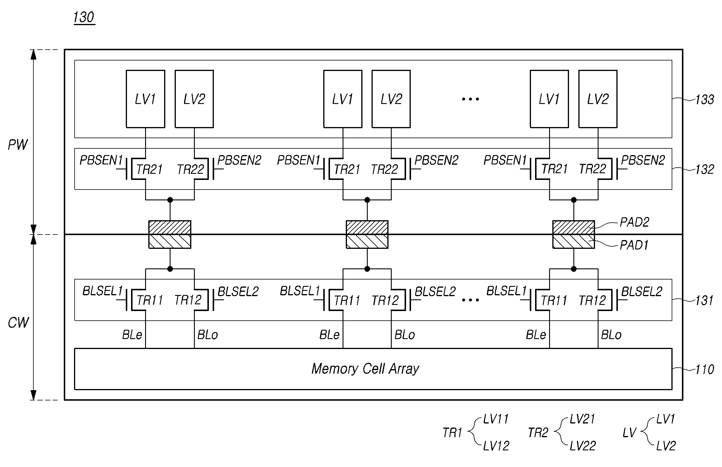
도 3을 참조하면, 페이지 버퍼 회로(130)는 비트 라인 선택 회로(131), 페이지 버퍼 고전압 회로(132) 및 페이지 버퍼 저전압 회로(133)를 포함할 수 있다.Referring to FIG. 3, the page buffer circuit (130) may include a bit line selection circuit (131), a page buffer high voltage circuit (132), and a page buffer low voltage circuit (133).
비트 라인 선택 회로(131)는 복수의 비트 라인들(BL)에 각각 연결되는 복수의 선택 트랜지스터들(TR1)을 포함할 수 있다. 선택 트랜지스터들(TR1) 각각은 비트 라인(BL)과 비트 라인 연결 노드(BLCM) 사이에 연결될 수 있다. 비트 라인 연결 노드들(BLCM) 각각에 2조의 선택 트랜지스터들(TR1)이 공통으로 연결될 수 있다. The bit line selection circuit (131) may include a plurality of selection transistors (TR1) each connected to a plurality of bit lines (BL). Each of the selection transistors (TR1) may be connected between a bit line (BL) and a bit line connection node (BLCM). Two sets of selection transistors (TR1) may be commonly connected to each of the bit line connection nodes (BLCM).
선택 트랜지스터들(TR1) 각각은 비트 라인 선택 신호에 응답하여 비트 라인(BL)과 비트 라인 연결 노드(BLCM)를 전기적으로 연결할 수 있다. 하나의 비트 라인 연결 노드(BLCM)에 공통으로 연결되는 2조의 선택 트랜지스터들(TR1)에 제공되는 비트 라인 선택 신호는 서로 다른 시점에 활성화될 수 있다. 하나의 비트 라인 연결 노드(BLCM)에 공통으로 연결되는 2조의 선택 트랜지스터들(TR1)의 하나에 제공되는 비트 라인 선택 신호가 활성화되는 경우, 다른 하나에 제공되는 비트 라인 선택 신호는 비활성화될 수 있다. Each of the selection transistors (TR1) can electrically connect a bit line (BL) and a bit line connection node (BLCM) in response to a bit line selection signal. The bit line selection signals provided to two sets of selection transistors (TR1) commonly connected to one bit line connection node (BLCM) can be activated at different times. When the bit line selection signal provided to one of the two sets of selection transistors (TR1) commonly connected to one bit line connection node (BLCM) is activated, the bit line selection signal provided to the other one can be deactivated.
페이지 버퍼 고전압 회로(132)는 복수의 비트 라인들(BL)에 각각 대응하는 복수의 센싱 트랜지스터들(TR2)을 포함할 수 있다. 센싱 트랜지스터들(TR2) 각각은 비트 라인 연결 노드(BLCM)와 센싱 노드(SO) 사이에 연결될 수 있다. 비트 라인 연결 노드들(BLCM) 각각에 2조의 센싱 트랜지스터들(TR2)이 공통으로 연결될 수 있다. The page buffer high voltage circuit (132) may include a plurality of sensing transistors (TR2) each corresponding to a plurality of bit lines (BL). Each of the sensing transistors (TR2) may be connected between a bit line connection node (BLCM) and a sensing node (SO). Two sets of sensing transistors (TR2) may be commonly connected to each of the bit line connection nodes (BLCM).
센싱 트랜지스터들(TR2) 각각은 비트 라인 센싱 신호에 응답하여 비트 라인 연결 노드(BLCM)와 센싱 노드(SO)를 전기적으로 연결할 수 있다. 하나의 비트 라인 연결 노드(BLCM)에 공통으로 연결된 2조의 센싱 트랜지스터들(TR2)에 제공되는 비트 라인 센싱 신호는 서로 다른 시점에 활성화될 수 있다. 하나의 비트 라인 연결 노드(BLCM)에 공통으로 연결된 2조의 센싱 트랜지스터들(TR2)의 하나에 제공되는 비트 라인 센싱 신호가 활성화되는 경우, 다른 하나에 제공되는 비트 라인 센싱 신호는 비활성화될 수 있다. Each of the sensing transistors (TR2) can electrically connect a bit line connection node (BLCM) and a sensing node (SO) in response to a bit line sensing signal. The bit line sensing signals provided to two sets of sensing transistors (TR2) commonly connected to one bit line connection node (BLCM) can be activated at different times. When the bit line sensing signal provided to one of the two sets of sensing transistors (TR2) commonly connected to one bit line connection node (BLCM) is activated, the bit line sensing signal provided to the other one can be deactivated.
페이지 버퍼 저전압 회로(133)는 복수의 비트 라인들(BL)에 각각 대응하는 복수의 페이지 버퍼 저전압 유닛들(LV)을 포함할 수 있다. 페이지 버퍼 저전압 유닛들(LV)은 센싱 노드들(SO)에 각각 연결될 수 있다. The page buffer low voltage circuit (133) may include a plurality of page buffer low voltage units (LV) each corresponding to a plurality of bit lines (BL). The page buffer low voltage units (LV) may be connected to sensing nodes (SO), respectively.
페이지 버퍼 저전압 유닛들(LV) 각각은 래치를 포함할 수 있다. 페이지 버퍼 저전압 유닛들(LV) 각각은 래치에 저장된 데이터에 기반하여 센싱 노드(SO)에 전압을 인가할 수 있다. 센싱 노드(SO)에 인가되는 전압은 페이지 버퍼 고전압 회로(132) 및 비트 라인 선택 회로(131)를 통해서 대응하는 비트 라인(BL)에 전달될 수 있다. Each of the page buffer low voltage units (LV) may include a latch. Each of the page buffer low voltage units (LV) may apply a voltage to a sensing node (SO) based on data stored in the latch. The voltage applied to the sensing node (SO) may be transmitted to a corresponding bit line (BL) through a page buffer high voltage circuit (132) and a bit line selection circuit (131).
페이지 버퍼 저전압 유닛들(LV)의 래치들은 센싱 노드들(SO)의 전압들에 기반하여 래치를 수행할 수 있다. 비트 라인 선택 회로(131) 및 페이지 버퍼 고전압 회로(132)를 통해서 비트 라인들(BL)로부터 센싱 노드들(SO)에 전달되는 전압들에 기반하여 래치가 수행될 수 있다. The latches of the page buffer low voltage units (LV) can perform latching based on the voltages of the sensing nodes (SO). The latching can be performed based on the voltages transmitted from the bit lines (BL) to the sensing nodes (SO) through the bit line selection circuit (131) and the page buffer high voltage circuit (132).
도 4는 본 발명의 일 실시예에 따른 메모리 장치를 개략적으로 나타낸 단면도이다.FIG. 4 is a cross-sectional view schematically illustrating a memory device according to one embodiment of the present invention.
도 4를 참조하면, 본 발명의 일 실시예에 따른 메모리 장치(100)는 셀 웨이퍼(CW) 및 셀 웨이퍼(CW) 상에 본딩된 페리 웨이퍼(PW)를 포함할 수 있다. Referring to FIG. 4, a memory device (100) according to one embodiment of the present invention may include a cell wafer (CW) and a peripheral wafer (PW) bonded on the cell wafer (CW).
셀 웨이퍼(CW)는 메모리 셀 어레이(110) 및 비트 라인 선택 회로(131)를 포함할 수 있다. 셀 웨이퍼(CW)는 페리 웨이퍼(PW)와 본딩되는 일면에 비트 라인 선택 회로(131)에 연결되는 복수의 제1 패드들(PAD1)을 포함할 수 있다. A cell wafer (CW) may include a memory cell array (110) and a bit line selection circuit (131). The cell wafer (CW) may include a plurality of first pads (PAD1) connected to the bit line selection circuit (131) on one surface of the cell wafer (CW) that is bonded to the peripheral wafer (PW).
비트 라인 선택 회로(131)의 선택 트랜지스터들(TR1)은 이븐 비트 라인들(BLe)에 연결된 제1 선택 트랜지스터들(TR11)과 오드 비트 라인들(BLo)에 연결된 제2 선택 트랜지스터들(TR12)로 구분될 수 있다. The selection transistors (TR1) of the bit line selection circuit (131) can be divided into first selection transistors (TR11) connected to even bit lines (BLe) and second selection transistors (TR12) connected to odd bit lines (BLo).
복수의 제1 패드들(PAD1) 각각은 제1 선택 트랜지스터들(TR11)의 하나 및 제2 선택 트랜지스터들(TR12)의 하나에 공통으로 연결될 수 있다. 이러한 경우, 제1 패드들(PAD1)의 개수는 비트 라인들(BL)의 개수의 절반일 수 있다.Each of the plurality of first pads (PAD1) may be commonly connected to one of the first selection transistors (TR11) and one of the second selection transistors (TR12). In this case, the number of first pads (PAD1) may be half of the number of bit lines (BL).
제1 선택 트랜지스터들(TR11)은 제1 비트 라인 선택 신호(BLSEL1)에 응답하여 이븐 비트 라인들(BLe)과 제1 패드들(PAD1)을 전기적으로 연결할 수 있다. 제2 선택 트랜지스터들(TR12)은 제2 비트 라인 선택 신호(BLSEL2)에 응답하여 오드 비트 라인들(BLo)과 제1 패드들(PAD1)을 전기적으로 연결할 수 있다. The first selection transistors (TR11) can electrically connect the even bit lines (BLe) and the first pads (PAD1) in response to the first bit line selection signal (BLSEL1). The second selection transistors (TR12) can electrically connect the odd bit lines (BLo) and the first pads (PAD1) in response to the second bit line selection signal (BLSEL2).
제1 비트 라인 선택 신호(BLSEL1)와 제2 비트 라인 선택 신호(BLSEL2)는 서로 다른 시점에 활성화될 수 있다. 제1 비트 라인 선택 신호(BLSEL1)가 활성화되고 제2 비트 라인 선택 신호(BLSEL2)가 비활성화되면, 제1 선택 트랜지스터들(TR11)은 이븐 비트 라인들(BLe)과 제1 패드들(PAD1)을 전기적으로 연결할 수 있고, 제2 선택 트랜지스터들(TR12)은 오드 비트 라인들(BLo)과 제1 패드들(PAD1)을 전기적으로 분리할 수 있다. The first bit line select signal (BLSEL1) and the second bit line select signal (BLSEL2) can be activated at different times. When the first bit line select signal (BLSEL1) is activated and the second bit line select signal (BLSEL2) is deactivated, the first select transistors (TR11) can electrically connect the even bit lines (BLe) and the first pads (PAD1), and the second select transistors (TR12) can electrically isolate the odd bit lines (BLo) and the first pads (PAD1).
역으로, 제2 비트 라인 선택 신호(BLSEL2)가 활성화되고 제1 비트 라인 선택 신호(BLSEL1)가 비활성화되면, 제2 선택 트랜지스터들(TR12)은 오드 비트 라인들(BLo)과 제1 패드들(PAD1)을 전기적으로 연결할 수 있고, 제1 선택 트랜지스터들(TR11)은 이븐 비트 라인들(BLe)과 제1 패드들(PAD1)을 전기적으로 분리할 수 있다.Conversely, when the second bit line select signal (BLSEL2) is activated and the first bit line select signal (BLSEL1) is deactivated, the second select transistors (TR12) can electrically connect the odd bit lines (BLo) and the first pads (PAD1), and the first select transistors (TR11) can electrically isolate the even bit lines (BLe) and the first pads (PAD1).
페리 웨이퍼(PW)는 페이지 버퍼 고전압 회로(132) 및 페이지 버퍼 저전압 회로(133)를 포함할 수 있다. 도시하지 않았지만, 페리 웨이퍼(PW)는 로우 디코더(도 1의 120) 및 주변 회로(도 1의 140)를 더 포함할 수 있다. The ferry wafer (PW) may include a page buffer high voltage circuit (132) and a page buffer low voltage circuit (133). Although not shown, the ferry wafer (PW) may further include a row decoder (120 of FIG. 1) and peripheral circuits (140 of FIG. 1).
페이지 버퍼 저전압 회로(133)의 페이지 버퍼 저전압 유닛들(LV)은 이븐 비트 라인들(BLe)에 대응하는 복수의 제1 페이지 버퍼 저전압 유닛들(LV1)과, 오드 비트 라인들(BLo)에 대응하는 제2 페이지 버퍼 저전압 유닛들(LV2)로 구분될 수 있다. 페리 웨이퍼(PW)는 셀 웨이퍼(CW)와 본딩되는 일측면에 복수의 제1 패드들(PAD1)에 각각 연결되는 복수의 제2 패드들(PAD2)을 포함할 수 있다. 제2 패드들(PAD2)의 개수는 제1 패드들(PAD1)의 개수와 동일할 수 있으며, 비트 라인들(BL)의 개수의 절반일 수 있다.The page buffer low voltage units (LV) of the page buffer low voltage circuit (133) may be divided into a plurality of first page buffer low voltage units (LV1) corresponding to even bit lines (BLe) and second page buffer low voltage units (LV2) corresponding to odd bit lines (BLo). The peripheral wafer (PW) may include a plurality of second pads (PAD2) respectively connected to a plurality of first pads (PAD1) on one side of the peripheral wafer (PW) bonded to the cell wafer (CW). The number of the second pads (PAD2) may be the same as the number of the first pads (PAD1) and may be half the number of the bit lines (BL).
페이지 버퍼 고전압 회로(132)의 센싱 트랜지스터들(TR2)은 이븐 비트 라인들(BLe)에 대응하는 제1 센싱 트랜지스터들(TR21) 및 오드 비트 라인들(BLo)에 대응하는 제2 센싱 트랜지스터들(TR22)로 구분될 수 있다. The sensing transistors (TR2) of the page buffer high voltage circuit (132) can be divided into first sensing transistors (TR21) corresponding to even bit lines (BLe) and second sensing transistors (TR22) corresponding to odd bit lines (BLo).
복수의 제2 패드들(PAD2) 각각은 제1 센싱 트랜지스터들(TR21)의 하나 및 제2 센싱 트랜지스터들(TR22)의 하나에 공통으로 연결될 수 있다. 제1 센싱 트랜지스터들(TR21)은 제1 페이지 버퍼 저전압 유닛들(LV1)과 제2 패드들(PAD2) 사이에 연결되며, 제1 비트 라인 센싱 신호(PBSEN1)에 응답하여 제1 페이지 버퍼 저전압 유닛들(LV1)과 제2 패드들(PAD2)을 전기적으로 연결할 수 있다. 제2 센싱 트랜지스터들(TR22)은 제2 페이지 버퍼 저전압 유닛들(LV2)과 제2 패드들(PAD2) 사이에 연결되며, 제2 비트 라인 센싱 신호(PBSEN2)에 응답하여 제2 페이지 버퍼 저전압 유닛들(LV2)과 제2 패드들(PAD2)을 전기적으로 연결할 수 있다. Each of the plurality of second pads (PAD2) may be commonly connected to one of the first sensing transistors (TR21) and one of the second sensing transistors (TR22). The first sensing transistors (TR21) are connected between the first page buffer low voltage units (LV1) and the second pads (PAD2) and may electrically connect the first page buffer low voltage units (LV1) and the second pads (PAD2) in response to a first bit line sensing signal (PBSEN1). The second sensing transistors (TR22) are connected between the second page buffer low voltage units (LV2) and the second pads (PAD2) and may electrically connect the second page buffer low voltage units (LV2) and the second pads (PAD2) in response to a second bit line sensing signal (PBSEN2).
제1 비트 라인 센싱 신호(PBSEN1)와 제2 비트 라인 센싱 신호(PBSEN2)는 서로 다른 시점에 활성화될 수 있다. 제1 비트 라인 센싱 신호(PBSEN1)가 활성화되고 제2 비트 라인 센싱 신호(PBSEN2)가 비활성화되면, 제1 센싱 트랜지스터들(TR21)은 제1 페이지 버퍼 저전압 유닛들(LV1)과 제2 패드들(PAD2)을 전기적으로 연결할 수 있고, 제2 센싱 트랜지스터들(TR22)은 제2 페이지 버퍼 저전압 유닛들(LV2)과 제2 패드들(PAD2)을 전기적으로 분리할 수 있다. The first bit line sensing signal (PBSEN1) and the second bit line sensing signal (PBSEN2) can be activated at different times. When the first bit line sensing signal (PBSEN1) is activated and the second bit line sensing signal (PBSEN2) is deactivated, the first sensing transistors (TR21) can electrically connect the first page buffer low voltage units (LV1) and the second pads (PAD2), and the second sensing transistors (TR22) can electrically separate the second page buffer low voltage units (LV2) and the second pads (PAD2).
역으로, 제2 비트 라인 센싱 신호(PBSEN2)가 활성화되고 제1 비트 라인 센싱 신호(PBSEN1)가 비활성화되면, 제2 센싱 트랜지스터들(TR22)은 제2 페이지 버퍼 저전압 유닛들(LV2)과 제2 패드들(PAD2)을 전기적으로 연결할 수 있고, 제1 센싱 트랜지스터들(TR21)은 제1 페이지 버퍼 저전압 유닛들(LV1)과 제2 패드들(PAD2)을 전기적으로 분리할 수 있다.Conversely, when the second bit line sensing signal (PBSEN2) is activated and the first bit line sensing signal (PBSEN1) is deactivated, the second sensing transistors (TR22) can electrically connect the second page buffer low voltage units (LV2) and the second pads (PAD2), and the first sensing transistors (TR21) can electrically separate the first page buffer low voltage units (LV1) and the second pads (PAD2).
도 5는 본 발명에 따른 메모리 장치의 개략적인 배치를 나타낸 도면이다. FIG. 5 is a drawing showing a schematic layout of a memory device according to the present invention.
도 5를 참조하면, 셀 웨이퍼(CW)는 기판(10)을 포함할 수 있다. 기판(10)은 활성면 및 후면을 가질 수 있다. 도 5에서 기판(10)은 활성면이 위를 향하도록 배치되어 있다. 메모리 셀 어레이(110) 및 비트 라인 선택 회로(131)는 기판(10)의 활성면 상에 배치될 수 있다Referring to FIG. 5, the cell wafer (CW) may include a substrate (10). The substrate (10) may have an active surface and a back surface. In FIG. 5, the substrate (10) is arranged with the active surface facing upward. A memory cell array (110) and a bit line selection circuit (131) may be arranged on the active surface of the substrate (10).
메모리 셀 어레이(110) 및 비트 라인 선택 회로(131) 상부에 복수의 비트 라인들(BL)이 배치될 수 있다. 비트 라인들(BL)은 메모리 셀 어레이(110) 및 비트 라인 선택 회로(131)에 연결될 수 있다. 비트 라인들(BL) 각각은 비트 라인 컨택(BLCNT)을 통해서 대응하는 선택 트랜지스터(TR1)에 연결될 수 있다. A plurality of bit lines (BL) may be arranged above a memory cell array (110) and a bit line selection circuit (131). The bit lines (BL) may be connected to the memory cell array (110) and the bit line selection circuit (131). Each of the bit lines (BL) may be connected to a corresponding selection transistor (TR1) through a bit line contact (BLCNT).
제1 패드들(PAD1)은 페리 웨이퍼(PW)와 본딩되는 셀 웨이퍼(CW)의 일면에 배치될 수 있다. 예시적으로, 제1 패드들(PAD1)은 셀 웨이퍼(CW)의 일면 가장자리에 제1 방향(FD)을 따라서 배치될 수 있다. 제1 패드들(PAD1) 각각은 제1 컨택(CNT1)을 통해서 대응하는 한 쌍의 선택 트랜지스터들(TR1)에 연결될 수 있고, 대응하는 한 쌍의 선택 트랜지스터들(TR1)을 통해서 대응하는 이븐 비트 라인(BLe) 및 대응하는 오드 비트 라인(BLo)에 연결될 수 있다. 제1 패드(PAD1)를 공유하는 이븐 비트 라인(BLe) 및 오드 비트 라인(BLo)은 서로 이웃하여 배치될 수 있다. The first pads (PAD1) may be arranged on one surface of the cell wafer (CW) to be bonded to the ferry wafer (PW). For example, the first pads (PAD1) may be arranged along the first direction (FD) at an edge of one surface of the cell wafer (CW). Each of the first pads (PAD1) may be connected to a corresponding pair of selection transistors (TR1) through a first contact (CNT1), and may be connected to a corresponding even bit line (BLe) and a corresponding odd bit line (BLo) through the corresponding pair of selection transistors (TR1). The even bit line (BLe) and the odd bit line (BLo) sharing the first pad (PAD1) may be arranged adjacent to each other.
페리 웨이퍼(PW)는 기판(30)을 포함할 수 있다. 기판(30)은 활성면 및 활성면과 대향하는 후면을 가질 수 있다. 도 5에서 기판(30)은 활성면이 아래를 향하도록 배치되어 있다. 페이지 버퍼 고전압 회로(132) 및 페이지 버퍼 저전압 회로(133)는 기판(30)의 활성면 상에 배치될 수 있다. A ferry wafer (PW) may include a substrate (30). The substrate (30) may have an active surface and a back surface facing the active surface. In FIG. 5, the substrate (30) is positioned with the active surface facing downward. A page buffer high voltage circuit (132) and a page buffer low voltage circuit (133) may be positioned on the active surface of the substrate (30).
제2 패드들(PAD2)은 셀 웨이퍼(CW)와 본딩되는 페리 웨이퍼(PW)의 일측면에 배치될 수 있다. 예시적으로, 제2 패드들(PAD2)은 페리 웨이퍼(PW)의 일측면 가장자리에 제1 방향(FD)을 따라서 배치될 수 있다. The second pads (PAD2) may be arranged on one side of the ferry wafer (PW) to be bonded to the cell wafer (CW). For example, the second pads (PAD2) may be arranged along the first direction (FD) on one side edge of the ferry wafer (PW).
제2 패드들(PAD2) 각각은 제2 컨택(CNT2)을 통해서 대응하는 한 쌍의 센싱 트랜지스터들(TR2)에 연결될 수 있으며, 대응하는 한 쌍의 센싱 트랜지스터들(TR2)을 통해서 대응하는 제1 페이지 버퍼 저전압 유닛(LV1) 및 대응하는 제2 페이지 버퍼 저전압 유닛(LV2)에 연결될 수 있다. 하나의 제1 페이지 버퍼 저전압 유닛(LV1) 및 하나의 제2 페이지 버퍼 저전압 유닛(LV2)가 하나의 제2 패드(PAD2)를 공유할 수 있다. Each of the second pads (PAD2) can be connected to a corresponding pair of sensing transistors (TR2) through a second contact (CNT2), and can be connected to a corresponding first page buffer low voltage unit (LV1) and a corresponding second page buffer low voltage unit (LV2) through the corresponding pair of sensing transistors (TR2). One first page buffer low voltage unit (LV1) and one second page buffer low voltage unit (LV2) can share one second pad (PAD2).
이해를 돕기 위하여, 도 5 및 후술되는 도 6, 도 8, 도 9에는 셀 웨이퍼(CW)와 페리 웨이퍼(PW)가 서로 분리된 것으로 도시되어 있으나, 셀 웨이퍼(CW)의 상면과 페리 웨이퍼(PW)의 하면이 서로 접하고 있는 것으로 이해되어야 할 것이다.To aid understanding, the cell wafer (CW) and the ferry wafer (PW) are depicted as being separated from each other in FIG. 5 and FIG. 6, FIG. 8, and FIG. 9 described below, but it should be understood that the upper surface of the cell wafer (CW) and the lower surface of the ferry wafer (PW) are in contact with each other.
도 6은 도 5의 선택 트랜지스터들 및 센싱 트랜지스터들의 배치를 예시하는 도면이다.FIG. 6 is a diagram illustrating the arrangement of selection transistors and sensing transistors of FIG. 5.
도 6을 참조하면, 비트 라인 선택 회로(131)에 포함된 선택 트랜지스터들(TR1)이 이븐 비트 라인들(BLe)에 연결된 제1 선택 트랜지스터들(TR11) 과 오드 비트 라인들(BLo)에 연결된 제2 선택 트랜지스터들(TR12)로 구분되어, 서로 다른 행에 배치될 수 있다. 이븐 비트 라인들(BLe)에 연결된 제1 선택 트랜지스터들(TR11)이 첫 번째 행에 배치될 수 있고, 오드 비트 라인들(BLo)에 연결된 제2 선택 트랜지스터들(TR12)이 두 번째 행에 배치될 수 있다.Referring to FIG. 6, selection transistors (TR1) included in a bit line selection circuit (131) may be divided into first selection transistors (TR11) connected to even bit lines (BLe) and second selection transistors (TR12) connected to odd bit lines (BLo), and may be arranged in different rows. The first selection transistors (TR11) connected to even bit lines (BLe) may be arranged in a first row, and the second selection transistors (TR12) connected to odd bit lines (BLo) may be arranged in a second row.
제1 선택 트랜지스터들(TR11)은 행 방향, 즉 제1 방향(FD)으로 연장되는 하나의 게이트 라인(G11)을 공유할 수 있고, 제2 선택 트랜지스터들(TR12)은 제1 방향(FD)으로 연장되는 하나의 게이트 라인(G12)을 공유할 수 있다. 제1 선택 트랜지스터들(TR11)은 게이트 라인(G11)에 인가되는 신호에 응답하여 일괄적으로 턴 온되거나 턴 오프될 수 있다. 제2 선택 트랜지스터들(TR12)은 게이트 라인(G12)에 인가되는 신호에 응답하여 일괄적으로 턴 온되거나 턴 오프될 수 있다. The first selection transistors (TR11) can share one gate line (G11) extending in the row direction, i.e., the first direction (FD), and the second selection transistors (TR12) can share one gate line (G12) extending in the first direction (FD). The first selection transistors (TR11) can be collectively turned on or off in response to a signal applied to the gate line (G11). The second selection transistors (TR12) can be collectively turned on or off in response to a signal applied to the gate line (G12).
페이지 버퍼 고전압 회로(132)에 포함된 센싱 트랜지스터들(TR2)이 이븐 비트 라인들(BLe)에 대응하는 제1 센싱 트랜지스터들(TR21)과 오드 비트 라인들(BLo)에 대응하는 제2 센싱 트랜지스터들(TR22)로 구분되어, 서로 다른 행에 배치될 수 있다. 예시적으로, 제1 페이지 버퍼 저전압 유닛들(LV1)에 연결된 제1 센싱 트랜지스터들(TR21)이 첫 번째 행에 배치될 수 있고, 제2 페이지 버퍼 저전압 유닛들(LV2)에 연결된 제2 센싱 트랜지스터들(TR22)이 두 번째 행에 배치될 수 있다.Sensing transistors (TR2) included in the page buffer high-voltage circuit (132) may be divided into first sensing transistors (TR21) corresponding to even bit lines (BLe) and second sensing transistors (TR22) corresponding to odd bit lines (BLo), and may be arranged in different rows. For example, first sensing transistors (TR21) connected to first page buffer low-voltage units (LV1) may be arranged in a first row, and second sensing transistors (TR22) connected to second page buffer low-voltage units (LV2) may be arranged in a second row.
제1 센싱 트랜지스터들(TR21)은 행 방향인 제1방향(FD)으로 연장되는 하나의 게이트 라인(G21)을 공유할 수 있다. 제2 센싱 트랜지스터들(TR22)은 제1방향(FD)으로 연장되는 하나의 게이트 라인(G22)을 공유할 수 있다. 제1 센싱 트랜지스터들(TR21)은 게이트 라인(G21)에 인가되는 신호에 응답하여 일괄적으로 턴 온되거나 턴 오프될 수 있고, 제2 센싱 트랜지스터들(TR22)은 게이트 라인(G22)에 인가되는 신호에 응답하여 일괄적으로 턴 온되거나 턴 오프될 수 있다. The first sensing transistors (TR21) can share one gate line (G21) extending in a first direction (FD), which is a row direction. The second sensing transistors (TR22) can share one gate line (G22) extending in the first direction (FD). The first sensing transistors (TR21) can be collectively turned on or off in response to a signal applied to the gate line (G21), and the second sensing transistors (TR22) can be collectively turned on or off in response to a signal applied to the gate line (G22).
도 7a는 도 6의 선택 트랜지스터들, 비트 라인 컨택 및 제1 컨택들의 배치를 예시하는 평면도이다.FIG. 7a is a plan view illustrating the arrangement of the selection transistors, bit line contacts, and first contacts of FIG. 6.
도 7a를 참조하면, 기판(10)에 복수의 활성 영역들(ACT1)이 제 1 방향(FD)을 따라서 나열될 수 있다. 게이트 라인들(G11,G12)이 제1 방향(FD)으로 활성 영역들(ACT1)을 가로지르며 서로 나란하게 배치될 수 있다. 게이트 라인들(G11,G12) 양측 활성 영역들(ACT1)에 불순물이 주입되어, 접합 영역들(Jn11-Jn13)이 형성될 수 있다. Referring to FIG. 7a, a plurality of active regions (ACT1) may be arranged along a first direction (FD) on a substrate (10). Gate lines (G11, G12) may be arranged parallel to each other while crossing the active regions (ACT1) in the first direction (FD). Impurities may be injected into the active regions (ACT1) on both sides of the gate lines (G11, G12) to form junction regions (Jn11-Jn13).
게이트 라인(G11) 및 게이트 라인(G11) 양측 접합 영역들(Jn11,Jn12)은 제1 선택 트랜지스터(TR11)를 구성할 수 있다. 게이트 라인(G12) 및 게이트 라인(G12) 양측 접합 영역들(Jn11,Jn13)은 제2 선택 트랜지스터(TR12)를 구성할 수 있다. 하나의 활성 영역(ACT1)에 배치되는 제1 선택 트랜지스터(TR11) 및 제2 선택 트랜지스터(TR12)는 하나의 접합 영역(Jn11)을 공유할 수 있다. 접합 영역(Jn11)은 컨택(CNT1)을 통해서 제1 패드(도 5의 PAD1)에 연결될 수 있다.The gate line (G11) and the junction regions (Jn11, Jn12) on both sides of the gate line (G11) can form a first selection transistor (TR11). The gate line (G12) and the junction regions (Jn11, Jn13) on both sides of the gate line (G12) can form a second selection transistor (TR12). The first selection transistor (TR11) and the second selection transistor (TR12) arranged in one active region (ACT1) can share one junction region (Jn11). The junction region (Jn11) can be connected to a first pad (PAD1 of FIG. 5) through a contact (CNT1).
제1 방향(FD)을 따라서 나열되는 복수의 활성 영역들(ACT1)에 대응하여, 복수의 제1 선택 트랜지스터들(TR11)이 게이트 라인(G11)을 따라서 제1 방향(FD)으로 나열될 수 있다. 제1 방향(FD)을 따라서 나열되는 복수의 활성 영역들(ACT1)에 대응하여, 복수의 제2 선택 트랜지스터들(TR12)이 게이트 라인(G12)을 따라서 제1 방향(FD)으로 나열될 수 있다. Corresponding to a plurality of active regions (ACT1) arranged along the first direction (FD), a plurality of first selection transistors (TR11) may be arranged along the gate line (G11) in the first direction (FD). Corresponding to a plurality of active regions (ACT1) arranged along the first direction (FD), a plurality of second selection transistors (TR12) may be arranged along the gate line (G12) in the first direction (FD).
비트 라인들(BL)이 제1,제2 선택 트랜지스터(TR11,TR12) 상에 배치될 수 있다. 비트 라인들(BL)은 제2 방향(SD)으로 신장되고 제1 방향(FD)을 따라서 나열될 수 있다. 제1 선택 트랜지스터들(TR11)의 접합 영역들(Jn2) 및 제2 선택 트랜지스터들(TR12)의 접합 영역들(Jn3) 각각은 비트 라인 컨택(BLCNT)을 통해서 대응하는 비트 라인(BL)에 연결될 수 있다. Bit lines (BL) may be arranged on the first and second selection transistors (TR11, TR12). The bit lines (BL) may extend in the second direction (SD) and be arranged along the first direction (FD). Each of the junction regions (Jn2) of the first selection transistors (TR11) and the junction regions (Jn3) of the second selection transistors (TR12) may be connected to a corresponding bit line (BL) through a bit line contact (BLCNT).
선택 트랜지스터들(TR11,TR12)이 이븐 비트 라인들(BLe)에 연결된 제1 선택 트랜지스터들(TR11)과 오드 비트 라인들(BLo)에 연결된 제2 선택 트랜지스터들(TR12)로 구분되어 서로 다른 행에 배치되므로, 제1 선택 트랜지스터들(TR11)의 접합 영역들(Jn2) 및 제2 선택 트랜지스터들(TR12)의 접합 영역들(Jn3)은 서로 다른 행에 배치될 것이다. 이에 따라, 제1 선택 트랜지스터들(TR11)의 접합 영역들(Jn2) 및 제2 선택 트랜지스터들(TR12)의 접합 영역들(Jn3)에 연결되는 비트 라인 컨택들(BLCNT)은 지그재그 형태를 이루면서 배치될 수 있다. 이러한 지그재그 형태의 배치는, 행 방향인 제1 방향(FD)으로 비트 라인 컨택들(BLCNT)이 서로 인접하지 않게 배치됨을 의미한다.Since the selection transistors (TR11, TR12) are arranged in different rows, divided into first selection transistors (TR11) connected to even bit lines (BLe) and second selection transistors (TR12) connected to odd bit lines (BLo), the junction regions (Jn2) of the first selection transistors (TR11) and the junction regions (Jn3) of the second selection transistors (TR12) will be arranged in different rows. Accordingly, the bit line contacts (BLCNT) connected to the junction regions (Jn2) of the first selection transistors (TR11) and the junction regions (Jn3) of the second selection transistors (TR12) can be arranged in a zigzag shape. This zigzag shape arrangement means that the bit line contacts (BLCNT) are arranged not adjacent to each other in the first direction (FD), which is the row direction.
메모리 장치의 집적도가 높아짐에 따라 비트 라인들(BL) 사이의 간격이 좁아지고 있다. 이러한 상황에서 동일한 행 내에서 두 비트 라인 컨택들이 서로 인접할 경우, 두 비트 라인 컨택들이 서로 단락(short)되는 불량이 발생할 가능성이 높다. 본 실시예에 의하면, 행 방향으로 비트 라인 컨택들(BLCNT)이 서로 인접하지 않게 배치되므로 비트 라인 컨택들(BLCNT)이 서로 단락되는 불량을 억제할 수 있다.As the integration of memory devices increases, the spacing between bit lines (BL) is narrowing. In this situation, if two bit line contacts are adjacent to each other in the same row, there is a high possibility that a defect in which the two bit line contacts are shorted to each other may occur. According to the present embodiment, since the bit line contacts (BLCNT) are arranged so as not to be adjacent to each other in the row direction, the defect in which the bit line contacts (BLCNT) are shorted to each other can be suppressed.
제1 방향(BL)에서 비트 라인들(BL)의 피치는 제1 크기(P1)을 가질 수 있다. 제1 방향(FD)에서 선택 트랜지스터들(TR1)의 피치는 제1 크기(P1)보다 큰 제2 크기(P2)를 가질 수 있다. In the first direction (BL), the pitch of the bit lines (BL) can have a first size (P1). In the first direction (FD), the pitch of the selection transistors (TR1) can have a second size (P2) larger than the first size (P1).
모든 선택 트랜지스터들을 비트 라인들이 나열된 방향인 제1 방향(FD)을 따라서 하나의 행에 배치할 경우, 선택 트랜지스터를 비트 라인의 피치에 대응하는 사이즈를 가지도록 구성해야 할 것이다. 이 경우, 집적도 증가로 비트 라인들의 피치가 감소하면, 선택 트랜지스터들의 사이즈가 매우 작아지게 되어 선택 트랜지스터 제조 공정의 마진이 타이트해지게 되고 제조 공정 동안에 불량이 발생할 확률이 높다. If all selection transistors are arranged in a single row along the first direction (FD) in which the bit lines are arranged, the selection transistors should be configured to have a size corresponding to the pitch of the bit lines. In this case, if the pitch of the bit lines decreases due to an increase in integration, the size of the selection transistors becomes very small, which tightens the margin of the selection transistor manufacturing process and increases the probability of defects occurring during the manufacturing process.
본 실시예에 의하면, 선택 트랜지스터들(TR1)이 제1 선택 트랜지스터들(TR11)과 제2 선택 트랜지스터들(TR12)로 구분되어 서로 다른 행에 배치되므로, 모든 선택 트랜지스터들(TR1)을 하나의 행에 배치하는 경우와 비교해서, 선택 트랜지스터(TR1)의 사이즈를 늘리는 것이 가능하다. 이에 따라, 선택 트랜지스터(TR1) 제조 공정의 마진이 향상되어, 선택 트랜지스터(TR1) 제조 공정 동안에 불량이 발생하는 것을 억제하는데 기여할 수 있다. According to the present embodiment, since the selection transistors (TR1) are divided into first selection transistors (TR11) and second selection transistors (TR12) and arranged in different rows, it is possible to increase the size of the selection transistors (TR1) compared to the case where all the selection transistors (TR1) are arranged in one row. Accordingly, the margin of the manufacturing process of the selection transistor (TR1) is improved, which can contribute to suppressing the occurrence of defects during the manufacturing process of the selection transistor (TR1).
비록, 본 실시예에서는 제1 선택 트랜지스터들(TR11)이 모두 같은 행에 배치되고, 제2 선택 트랜지스터들(TR12)이 모두 같은 행에 배치되는 경우를 나타내나, 이에 한정되는 것은 아니다. 제1 선택 트랜지스터들(TR11)이 2개 이상의 행에 나뉘어 배치되고, 제2 선택 트랜지스터들(TR12)이 2개 이상의 행에 나뉘어 배치될 수도 있다.Although the present embodiment shows a case where all of the first selection transistors (TR11) are arranged in the same row and all of the second selection transistors (TR12) are arranged in the same row, it is not limited thereto. The first selection transistors (TR11) may be arranged in two or more rows and the second selection transistors (TR12) may be arranged in two or more rows.
도 7b는 도 6의 센싱 트랜지스터들 및 제2 컨택들의 배치를 예시하는 평면도이다.FIG. 7b is a plan view illustrating the arrangement of the sensing transistors and second contacts of FIG. 6.
도 7b를 참조하면, 기판(30)에 복수의 활성 영역들(ACT2)이 제 1 방향(FD)을 따라서 나열될 수 있다. 게이트 라인들(G21,G22)이 제1 방향(FD)으로 활성 영역들(ACT2)을 가로지르며 서로 나란하게 배치될 수 있다. 게이트 라인들(G21,G22) 양측 활성 영역들(ACT2)에 불순물이 주입되어 접합 영역들(Jn21-Jn23)이 형성될 수 있다. Referring to FIG. 7b, a plurality of active regions (ACT2) may be arranged along the first direction (FD) on the substrate (30). Gate lines (G21, G22) may be arranged parallel to each other while crossing the active regions (ACT2) in the first direction (FD). Impurities may be injected into the active regions (ACT2) on both sides of the gate lines (G21, G22) to form junction regions (Jn21-Jn23).
게이트 라인(G21) 및 게이트 라인(G21) 양측 접합 영역들(Jn21,Jn22)은 제1 센싱 트랜지스터(TR21)를 구성할 수 있다. 게이트 라인(G22) 및 게이트 라인(G22) 양측 접합 영역들(Jn21,Jn23)은 제2 센싱 트랜지스터(TR22)를 구성할 수 있다. 하나의 활성 영역(ACT2)에 배치되는 제1 센싱 트랜지스터(TR21) 및 제2 센싱 트랜지스터(TR22)는 하나의 접합 영역(Jn21)을 공유할 수 있다. 접합 영역(Jn21)은 컨택(CNT2)을 통해서 제2 패드(도 5의 PAD2)에 연결될 수 있다.The gate line (G21) and the junction regions (Jn21, Jn22) on both sides of the gate line (G21) can form a first sensing transistor (TR21). The gate line (G22) and the junction regions (Jn21, Jn23) on both sides of the gate line (G22) can form a second sensing transistor (TR22). The first sensing transistor (TR21) and the second sensing transistor (TR22) arranged in one active region (ACT2) can share one junction region (Jn21). The junction region (Jn21) can be connected to a second pad (PAD2 in FIG. 5) through a contact (CNT2).
제1 방향(FD)을 따라서 나열되는 복수의 활성 영역들(ACT2)에 대응하여, 복수의 제1 센싱 트랜지스터들(TR21)이 게이트 라인(G21)을 따라서 제1 방향(FD)으로 나열될 수 있다. 제1 방향(FD)을 따라서 나열되는 복수의 활성 영역들(ACT2)에 대응하여, 복수의 제2 센싱 트랜지스터들(TR22)이 게이트 라인(G22)을 따라서 제1 방향(FD)으로 나열될 수 있다. A plurality of first sensing transistors (TR21) may be arranged in the first direction (FD) along the gate line (G21) corresponding to a plurality of active regions (ACT2) arranged along the first direction (FD). A plurality of second sensing transistors (TR22) may be arranged in the first direction (FD) along the gate line (G22) corresponding to a plurality of active regions (ACT2) arranged along the first direction (FD).
본 실시예에 의하면, 센싱 트랜지스터들(TR2)이 제1 센싱 트랜지스터들(TR21)과 제2 센싱 트랜지스터들(TR22)로 구분되어 서로 다른 행에 배치되므로, 모든 센싱 트랜지스터들(TR2)을 하나의 행에 배치하는 경우와 비교해서, 센싱 트랜지스터(TR2)의 사이즈를 늘리는 것이 가능하다. 이에 따라, 센싱 트랜지스터(TR2)의 제조 공정의 마진이 향상되고, 센싱 트랜지스터들(TR2) 제조 공정 중에 불량이 발생하는 것을 억제하는데 기여할 수 있다. According to the present embodiment, since the sensing transistors (TR2) are divided into first sensing transistors (TR21) and second sensing transistors (TR22) and arranged in different rows, it is possible to increase the size of the sensing transistors (TR2) compared to a case where all the sensing transistors (TR2) are arranged in one row. Accordingly, the margin of the manufacturing process of the sensing transistors (TR2) is improved, and it can contribute to suppressing the occurrence of defects during the manufacturing process of the sensing transistors (TR2).
비록 본 실시예에서는, 제1 센싱 트랜지스터들(TR21)이 모두 같은 행에 배치되고, 제2 센싱 트랜지스터들(TR22)이 모두 같은 행에 배치되는 경우를 나타내나, 이에 한정되는 것은 아니다. 제1 센싱 트랜지스터들(TR21)이 2개 이상의 행에 나뉘어 배치되고, 제2 센싱 트랜지스터들(TR22)이 2개 이상의 행에 나뉘어 배치될 수도 있다.Although the present embodiment shows a case where all of the first sensing transistors (TR21) are arranged in the same row and all of the second sensing transistors (TR22) are arranged in the same row, it is not limited thereto. The first sensing transistors (TR21) may be arranged in two or more rows and the second sensing transistors (TR22) may be arranged in two or more rows.
도 8은 본 발명에 따른 메모리 장치의 다른 예시를 나타내는 도면이다.FIG. 8 is a drawing showing another example of a memory device according to the present invention.
도 8을 참조하면, 복수의 제1 패드들(PAD1) 각각은 비트 라인 선택 회로(131)를 통해서 4개의 비트 라인들(BL)에 공통으로 연결될 수 있다. 이러한 경우, 4개의 비트 라인들(BL)이 하나의 제1 패드(PAD1)를 공유하는 것으로 정의될 수 있으며, 제1 패드들(PAD1)의 개수는 비트 라인들(BL)의 개수의 1/4일 수 있다. Referring to FIG. 8, each of the plurality of first pads (PAD1) may be commonly connected to four bit lines (BL) through a bit line selection circuit (131). In this case, it may be defined that the four bit lines (BL) share one first pad (PAD1), and the number of first pads (PAD1) may be 1/4 of the number of bit lines (BL).
비트 라인 선택 회로(131)의 선택 트랜지스터들(TR1)은 복수의 비트 라인 선택 그룹들로 그룹화될 수 있다. 단일 비트 라인 선택 그룹에 포함되는 선택 트랜지스터들(TR1)은 하나의 비트 라인 선택 신호에 응답하여 일괄적으로 턴 온되거나 턴오프될 수 있다. 단일 비트 라인 선택 그룹에 포함된 선택 트랜지스터들(TR1)이 동시에 턴 온되면, 턴 온된 선택 트랜지스터들(TR1)은 대응하는 비트 라인들(BL)의 데이터들을 병렬적으로 페이지 버퍼 고전압 회로(132)를 통해서 페이지 버퍼 저전압 회로(133)에 전달할 수 있다. The selection transistors (TR1) of the bit line selection circuit (131) can be grouped into a plurality of bit line selection groups. The selection transistors (TR1) included in a single bit line selection group can be turned on or off collectively in response to a single bit line selection signal. When the selection transistors (TR1) included in a single bit line selection group are turned on simultaneously, the turned-on selection transistors (TR1) can transfer data of the corresponding bit lines (BL) in parallel to the page buffer low voltage circuit (133) through the page buffer high voltage circuit (132).
하나의 제1 패드(PAD1)를 공유하는 선택 트랜지스터들(TR1)은 서로 다른 비트 라인 선택 그룹들에 포함될 수 있다. 하나의 제1 패드(PAD1)를 공유하는 선택 트랜지스터들(TR1)에 제공되는 비트 라인 선택 신호들은 서로 다른 시점에 활성화될 수 있다. 하나의 제1 패드(PAD1)를 공유하는 선택 트랜지스터들(TR1)에 제공되는 비트 라인 선택 신호들 중 어느 하나가 활성화되는 경우, 나머지들은 비활성화될 수 있다. The selection transistors (TR1) sharing one first pad (PAD1) can be included in different bit line selection groups. The bit line selection signals provided to the selection transistors (TR1) sharing one first pad (PAD1) can be activated at different times. When any one of the bit line selection signals provided to the selection transistors (TR1) sharing one first pad (PAD1) is activated, the others can be deactivated.
복수의 제2 패드들(PAD2) 각각은 제1 패드(PAD1) 및 비트 라인 선택 회로(131)를 통해서 4개의 비트 라인들(BL)에 공통으로 연결될 수 있다. 이러한 경우, 4개의 비트 라인들(BL)이 하나의 제2 패드(PAD2)를 공유하는 것으로 정의될 수 있으며, 제2 패드들(PAD2)의 개수는 비트 라인들(BL)의 개수의 1/4일 수 있다. Each of the plurality of second pads (PAD2) may be commonly connected to four bit lines (BL) through the first pad (PAD1) and the bit line selection circuit (131). In this case, it may be defined that the four bit lines (BL) share one second pad (PAD2), and the number of second pads (PAD2) may be 1/4 of the number of bit lines (BL).
페이지 버퍼 고전압 회로(132)의 센싱 트랜지스터들(TR2)은 복수의 비트 라인 센싱 그룹들로 그룹화될 수 있다. 단일 비트 라인 센싱 그룹에 포함되는 센싱 트랜지스터들(TR2)은 하나의 비트 라인 센싱 신호에 응답하여 일괄적으로 턴 온되거나 턴오프될 수 있다. 단일 비트 라인 센싱 그룹에 포함된 센싱 트랜지스터들(TR2)이 동시에 턴 온되면, 턴 온된 센싱 트랜지스터들(TR2)은 비트 라인 선택 회로(131)를 통해서 대응하는 비트 라인들(BL)로부터 제공되는 데이터들을 병렬적으로 페이지 버퍼 저전압 회로(133)에 전달할 수 있다. The sensing transistors (TR2) of the page buffer high-voltage circuit (132) can be grouped into a plurality of bit line sensing groups. The sensing transistors (TR2) included in a single bit line sensing group can be turned on or off collectively in response to a single bit line sensing signal. When the sensing transistors (TR2) included in the single bit line sensing group are turned on simultaneously, the turned-on sensing transistors (TR2) can transfer data provided from corresponding bit lines (BL) in parallel to the page buffer low-voltage circuit (133) through the bit line selection circuit (131).
하나의 제2 패드(PAD2)를 공유하는 센싱 트랜지스터들(TR2)은 서로 다른 비트 라인 센싱 그룹들에 포함될 수 있다. 하나의 제2 패드(PAD2)를 공유하는 센싱 트랜지스터들(TR2)에 제공되는 비트 라인 센싱 신호들은 서로 다른 시점에 활성화될 수 있다. 하나의 제2 패드(PAD2)를 공유하는 센싱 트랜지스터들(TR2)에 제공되는 비트 라인 센싱 신호들 중 어느 하나가 활성화되는 경우, 나머지들은 모두 비활성화될 수 있다. The sensing transistors (TR2) sharing one second pad (PAD2) can be included in different bit line sensing groups. The bit line sensing signals provided to the sensing transistors (TR2) sharing one second pad (PAD2) can be activated at different times. When any one of the bit line sensing signals provided to the sensing transistors (TR2) sharing one second pad (PAD2) is activated, the others can all be deactivated.
도 9는 도 8의 선택 트랜지스터들 및 센싱 트랜지스터들의 배치 구조를 예시하는 도면이다.FIG. 9 is a drawing illustrating the arrangement structure of the selection transistors and sensing transistors of FIG. 8.
도 9를 참조하면, 비트 라인 선택 회로(131)의 선택 트랜지스터들(TR1)이 복수의 비트 라인 선택 그룹들로 그룹화되어, 그룹 별로 서로 다른 행에 배치될 수 있다. 예시적으로, 선택 트랜지스터들(TR1)이 4개의 비트 라인 선택 그룹들로 그룹화되어, 4개의 행에 나뉘어 배치될 수 있다Referring to FIG. 9, the selection transistors (TR1) of the bit line selection circuit (131) may be grouped into a plurality of bit line selection groups and arranged in different rows for each group. For example, the selection transistors (TR1) may be grouped into four bit line selection groups and arranged in four rows.
단일 비트 라인 선택 그룹에 포함된 선택 트랜지스터들(TR1)은 행 방향, 즉 제1 방향(FD)으로 연장되는 하나의 게이트 라인(G1)을 공유할 수 있다. The selection transistors (TR1) included in a single bit line selection group can share one gate line (G1) extending in the row direction, i.e., the first direction (FD).
페이지 버퍼 고전압 회로(132)의 센싱 트랜지스터들(TR2)이 복수의 비트 라인 센싱 그룹들로 그룹화되어, 그룹 별로 서로 다른 행에 배치될 수 있다. 예시적으로, 센싱 트랜지스터들(TR2)이 4개의 비트 라인 센싱 그룹들로 그룹화되어, 4개의 행에 나뉘어 배치될 수 있다The sensing transistors (TR2) of the page buffer high voltage circuit (132) may be grouped into a plurality of bit line sensing groups and arranged in different rows for each group. For example, the sensing transistors (TR2) may be grouped into four bit line sensing groups and arranged in four rows.
하나의 비트 라인 센싱 그룹에 포함된 센싱 트랜지스터들(TR2)은 행 방향, 즉 제1 방향(FD)으로 연장되는 하나의 게이트 라인(G2)을 공유할 수 있다. Sensing transistors (TR2) included in one bit line sensing group can share one gate line (G2) extending in the row direction, i.e., the first direction (FD).
메모리 장치가 고용량화됨에 따라서 메모리 장치에 포함된 비트 라인들의 개수가 늘어나고 있다. 본 실시예에 의하면, 복수의 비트 라인들이 하나의 패드를 공유하므로, 비트 라인들이 개별적으로 패드를 사용하는 구조에 비해서, 패드의 개수를 절반으로 줄일 수 있다. 따라서, 패드의 사이즈를 늘리는 것이 가능하므로, 셀 웨이퍼와 페리 웨이퍼 간 본딩시에 패드 얼라인 마진이 향상되어 패드 연결 불량을 억제하는데 기여할 수 있다. As memory devices become more capable, the number of bit lines included in the memory devices is increasing. According to the present embodiment, since multiple bit lines share one pad, the number of pads can be reduced by half compared to a structure in which bit lines individually use pads. Accordingly, since the pad size can be increased, the pad alignment margin can be improved during bonding between the cell wafer and the peripheral wafer, which can contribute to suppressing pad connection failure.
3차원 구조의 도입으로 메모리 셀 어레이가 점유하는 레이아웃 면적은 감소되고 있다. 반면에, 성능 향상을 위하여 메모리 셀 어레이를 제어하는 로직 회로의 구조가 복잡해지고 점유 면적이 증가하고 있다. 이에 따라, 로직 회로의 배치에 필요한 레이아웃 면적이 메모리 셀 어레이의 배치에 필요한 레이아웃 면적보다 커지고 있다. 본 발명의 실시예들에 의하면, 로직 회로의 비트 라인 선택 회로를 셀 웨이퍼에 배치함으로써, 셀 웨이퍼와 페리 웨이퍼의 레이아웃 이용 효율을 높일 수 있고 이에 따라 메모리 장치의 사이즈를 축소시키는데 기여할 수 있다.With the introduction of a three-dimensional structure, the layout area occupied by a memory cell array is decreasing. On the other hand, in order to improve performance, the structure of a logic circuit that controls a memory cell array is becoming more complex and its occupied area is increasing. Accordingly, the layout area required for arranging a logic circuit is becoming larger than the layout area required for arranging a memory cell array. According to embodiments of the present invention, by arranging a bit line selection circuit of a logic circuit on a cell wafer, the layout utilization efficiency of the cell wafer and the peripheral wafer can be increased, thereby contributing to reducing the size of a memory device.
도 10은 본 발명의 실시예에 따른 메모리 장치를 포함한 메모리 시스템을 개략적으로 도시한 블록도이다.FIG. 10 is a block diagram schematically illustrating a memory system including a memory device according to an embodiment of the present invention.
도 10을 참조하면, 본 발명의 실시예에 따른 메모리 시스템(600)은 비휘발성 메모리 장치(610) 및 메모리 컨트롤러(620)를 포함할 수 있다.Referring to FIG. 10, a memory system (600) according to an embodiment of the present invention may include a nonvolatile memory device (610) and a memory controller (620).
비휘발성 메모리 장치(610)는 앞서 설명한 메모리 장치로 구성되고, 앞서 설명한 방법으로 동작될 수 있다. 메모리 컨트롤러(620)는 비휘발성 메모리 장치(610)를 제어하도록 구성될 것이다. 비휘발성 메모리 장치(610)와 메모리 컨트롤러(620)의 결합에 의해 메모리 카드 또는 반도체 디스크 장치(Solid State Disk: SSD)로 제공될 수 있을 것이다. SRAM(621)은 프로세싱 유닛(622)의 동작 메모리로써 사용된다. 호스트 인터페이스(623)는 메모리 시스템(600)과 접속되는 호스트의 데이터 교환 프로토콜을 구비한다.The nonvolatile memory device (610) is configured as the memory device described above and can be operated in the method described above. The memory controller (620) will be configured to control the nonvolatile memory device (610). The combination of the nonvolatile memory device (610) and the memory controller (620) can be provided as a memory card or a solid state disk (SSD). The SRAM (621) is used as an operating memory of the processing unit (622). The host interface (623) has a data exchange protocol of a host connected to the memory system (600).
에러 정정 블록(624)은 비휘발성 메모리 장치(610)로부터 독출된 데이터에 포함되는 에러를 검출 및 정정한다.The error correction block (624) detects and corrects errors contained in data read from the nonvolatile memory device (610).
메모리 인터페이스(625)는 본 발명의 비휘발성 메모리 장치(610)와 인터페이싱한다. 프로세싱 유닛(622)은 메모리 컨트롤러(620)의 데이터 교환을 위한 제반 제어 동작을 수행한다.The memory interface (625) interfaces with the nonvolatile memory device (610) of the present invention. The processing unit (622) performs all control operations for data exchange of the memory controller (620).
비록 도면에는 도시되지 않았지만, 본 발명에 따른 메모리 시스템(600)은 호스트(Host)와의 인터페이싱을 위한 코드 데이터를 저장하는 ROM(미도시됨) 등이 더 제공될 수 있음은 이 분야의 통상적인 지식을 습득한 자들에게 자명하다. 비휘발성 메모리 장치(620)는 복수의 플래시 메모리 칩들로 구성되는 멀티-칩 패키지로 제공될 수도 있다Although not shown in the drawing, it is obvious to those skilled in the art that the memory system (600) according to the present invention may further be provided with a ROM (not shown) for storing code data for interfacing with a host. The nonvolatile memory device (620) may also be provided as a multi-chip package composed of a plurality of flash memory chips.
이상의 본 발명의 메모리 시스템(600)은 에러의 발생 확률이 낮은 고신뢰성의 저장 매체로 제공될 수 있다. 특히, 최근 활발히 연구되고 있는 반도체 디스크 장치(Solid State Disk: 이하 SSD)와 같은 메모리 시스템에서 본 발명의 비휘발성 메모리 장치가 구비될 수 있다. 이 경우, 메모리 컨트롤러(620)는 USB, MMC, PCI-E,SATA, PATA, SCSI, ESDI, 그리고 IDE 등과 같은 다양한 인터페이스 프로토콜들 중 하나를 통해서 외부(예를 들면,호스트)와 통신하도록 구성될 것이다.The memory system (600) of the present invention can be provided as a highly reliable storage medium with a low probability of error occurrence. In particular, the nonvolatile memory device of the present invention can be provided in a memory system such as a solid state disk (SSD) that has been actively studied recently. In this case, the memory controller (620) will be configured to communicate with the outside (e.g., a host) through one of various interface protocols such as USB, MMC, PCI-E, SATA, PATA, SCSI, ESDI, and IDE.
도 11은 본 발명의 실시예에 따른 메모리 장치를 포함한 컴퓨팅 시스템을 개략적으로 보여주는 블록도이다.FIG. 11 is a block diagram schematically showing a computing system including a memory device according to an embodiment of the present invention.
도 11을 참조하면, 본 발명에 따른 컴퓨팅 시스템(700)은 시스템 버스(760)에 전기적으로 연결된 메모리 시스템(710), 마이크로프로세서(720), 램(730), 사용자 인터페이스(740), 베이스밴드 칩셋(Baseband chipset)과 같은 모뎀(750)을 포함할 수 있다 본 발명에 따른 컴퓨팅 시스템(700)이 모바일 장치인 경우, 컴퓨팅 시스템(700)의 동작 전압을 공급하기 위한 배터리(미도시됨)가 추가적으로 제공될 것이다. 비록 도면에는 도시되지 않았지만, 본 발명에 따른 컴퓨팅 시스템(700)에는 응용 칩셋(Application chipset), 카메라 이미지 프로세서(Camera Image Processor: CIS), 모바일 디램, 등이 더 제공될 수 있음은 이 분야의 통상적인 지식을 습득한 자들에게 자명하다. 메모리 시스템(710)은, 예를 들면, 데이터를 저장하는 데 비휘발성 메모리를 사용하는 SSD(Solid State Drive/Disk)를 구성할 수 있다. 또는, 메모리 시스템(710)은, 퓨전 플래시 메모리(예를 들면, 원낸드 플래시 메모리)로 제공될 수 있다.Referring to FIG. 11, a computing system (700) according to the present invention may include a memory system (710), a microprocessor (720), a RAM (730), a user interface (740), and a modem (750) such as a baseband chipset, all of which are electrically connected to a system bus (760). If the computing system (700) according to the present invention is a mobile device, a battery (not shown) for supplying an operating voltage of the computing system (700) may be additionally provided. Although not shown in the drawing, it will be apparent to those skilled in the art that the computing system (700) according to the present invention may further include an application chipset, a camera image processor (CIS), a mobile DRAM, and the like. The memory system (710) may, for example, configure an SSD (Solid State Drive/Disk) that uses nonvolatile memory to store data. Alternatively, the memory system (710) may be provided as a fusion flash memory (e.g., OneNAND flash memory).
이상에서 설명한 본 발명의 실시예는 장치 및 방법을 통해서만 구현이 되는 것은 아니며, 본 발명의 실시예 구성에 대응하는 기능을 실현하는 프로그램 또는 그 프로그램이 기록된 기록 매체를 통해서 구현될 수도 있으며, 이러한 구현은 앞서 설명한 실시예의 기재로부터 본 발명이 속하는 기술분야의 전문가라면 쉽게 구현할 수 있을 것이다.The embodiments of the present invention described above are not implemented only through devices and methods, but may also be implemented through a program that realizes a function corresponding to the configuration of the embodiments of the present invention or a recording medium on which the program is recorded, and such implementation will be easily implemented by a specialist in the technical field to which the present invention belongs based on the description of the embodiments described above.
앞서 설명한 본 발명의 상세한 설명에서는 본 발명의 실시예를 참조하여 설명하였지만, 해당 기술분야의 숙련된 당업자 또는 해당 기술분야에 통상의 지식을 갖는 자라면 후술 될 특허청구범위에 기재된 본 발명의 사상 및 기술 영역으로부터 벗어나지 않는 범위 내에서 본 발명을 다양하게 수정 및 변경시킬 수 있음을 이해할 수 있을 것이다.Although the detailed description of the present invention described above has been described with reference to embodiments of the present invention, it will be understood by those skilled in the art or having common knowledge in the art that various modifications and changes can be made to the present invention without departing from the spirit and technical scope of the present invention as set forth in the claims to be described later.
Claims (20)
상기 일면에 본딩되며 상기 셀 웨이퍼와 본딩되는 일측면에 상기 제1 패드와 연결되는 제2 패드를 구비하는 페리 웨이퍼;를 포함하며,
상기 셀 웨이퍼는, 메모리 셀 어레이;
상기 메모리 셀 어레이에 연결된 제1 비트 라인 및 제2 비트 라인; 및
상기 제1 비트 라인 및 상기 제2 비트 라인의 하나를 상기 제1 패드에 연결하는 비트 라인 선택 회로;를 포함하고,
상기 페리 웨이퍼는 상기 제1 비트 라인에 대응하는 제1 페이지 버퍼 저전압 유닛 및 상기 제2 비트 라인에 대응하는 제2 페이지 버퍼 저전압 유닛을 포함하는 페이지 버퍼 저전압 회로; 및
상기 제1 페이지 버퍼 저전압 유닛 및 상기 제2 페이지 버퍼 저전압 유닛의 하나를 상기 제2 패드에 연결하는 페이지 버퍼 고전압 회로;를 포함하는 메모리 장치.A cell wafer having a first pad on one side; and
A ferri wafer having a second pad connected to the first pad on one side thereof and bonded to the cell wafer;
The above cell wafer comprises a memory cell array;
a first bit line and a second bit line connected to the above memory cell array; and
a bit line selection circuit connecting one of the first bit line and the second bit line to the first pad;
The above ferry wafer comprises a page buffer low-voltage circuit including a first page buffer low-voltage unit corresponding to the first bit line and a second page buffer low-voltage unit corresponding to the second bit line; and
A memory device comprising: a page buffer high voltage circuit connecting one of the first page buffer low voltage unit and the second page buffer low voltage unit to the second pad.
상기 제2 비트 라인과 상기 제1 패드 사이에 연결되며 제2 비트 라인 선택 신호에 응답하여 상기 제2 비트 라인과 상기 제1 패드를 전기적으로 연결하는 제2 선택 트랜지스터;를 포함하며,
상기 제1 비트 라인 선택 신호와 상기 제2 비트 라인 선택 신호는 서로 다른 시점에 활성화되는 것을 특징으로 하는 메모리 장치.In the first paragraph, the bit line selection circuit comprises a first selection transistor connected between the first bit line and the first pad and electrically connecting the first bit line and the first pad in response to a first bit line selection signal; and
A second selection transistor is connected between the second bit line and the first pad and electrically connects the second bit line and the first pad in response to a second bit line selection signal;
A memory device, characterized in that the first bit line selection signal and the second bit line selection signal are activated at different times.
상기 제1 패드는 컨택을 통해서 상기 접합 영역에 연결되는 것을 특징으로 하는 메모리 장치.In the second paragraph, the first selection transistor and the second selection transistor share one junction region,
A memory device characterized in that the first pad is connected to the bonding area through a contact.
상기 제2 패드와 상기 제2 페이지 버퍼 저전압 유닛 사이에 연결되며 제2 비트 라인 센싱 신호에 응답하여 상기 제2 패드와 상기 제2 페이지 버퍼 저전압 유닛을 전기적으로 연결하는 제2 센싱 트랜지스터;를 포함하며,
상기 제1 비트 라인 센싱 신호와 상기 제2 비트 라인 센싱 신호는 서로 다른 시점에 활성화되는 것을 특징으로 하는 메모리 장치.In the first paragraph, the page buffer high voltage circuit is connected between the second pad and the first page buffer low voltage unit, and includes a first sensing transistor electrically connecting the second pad and the first page buffer low voltage unit in response to a first bit line sensing signal; and
A second sensing transistor is connected between the second pad and the second page buffer low voltage unit, and electrically connects the second pad and the second page buffer low voltage unit in response to a second bit line sensing signal;
A memory device, characterized in that the first bit line sensing signal and the second bit line sensing signal are activated at different times.
상기 제2 패드는 컨택을 통해서 상기 접합 영역에 연결되는 것을 특징으로 하는 메모리 장치.In the fourth paragraph, the first sensing transistor and the second sensing transistor share one junction region,
A memory device characterized in that the second pad is connected to the bonding area through a contact.
상기 복수의 전극층들 및 상기 복수의 층간절연층들을 관통하며 상기 제1 비트 라인 및 상기 제2 비트 라인에 연결된 복수의 수직 채널들;을 포함하는 것을 특징으로 하는 메모리 장치.In the first aspect, the memory cell array comprises a plurality of electrode layers and a plurality of interlayer insulating layers alternately stacked on a substrate; and
A memory device characterized by including a plurality of vertical channels penetrating the plurality of electrode layers and the plurality of interlayer insulating layers and connected to the first bit line and the second bit line.
상기 일면에 본딩되며 상기 셀 웨이퍼와 본딩되는 일측면에 상기 복수의 제1 패드들과 연결되는 복수의 제2 패드들을 구비하는 페리 웨이퍼;를 포함하며,
상기 셀 웨이퍼는, 메모리 셀 어레이;
상기 메모리 셀 어레이에 연결되며 복수의 제1 비트 라인들 및 복수의 제2 비트 라인들을 포함하는 복수의 비트 라인들; 및
상기 복수의 제1 비트 라인들 또는 상기 복수의 제2 비트 라인들을 상기 복수의 제1 패드들에 연결하는 비트 라인 선택 회로;를 포함하고,
상기 페리 웨이퍼는, 상기 복수의 제1 비트 라인들에 대응하는 복수의 제1 페이지 버퍼 저전압 유닛들 및 상기 복수의 제2 비트 라인들에 대응하는 복수의 제2 페이지 버퍼 저전압 유닛들을 포함하는 페이지 버퍼 저전압 회로; 및
상기 복수의 제1 페이지 버퍼 저전압 유닛들 또는 상기 복수의 제2 페이지 버퍼 저전압 유닛들을 상기 복수의 제2 패드들에 연결하는 페이지 버퍼 고전압 회로;를 포함하는 메모리 장치. A cell wafer having a plurality of first pads on one side; and
A ferri wafer having a plurality of second pads bonded to the one side and connected to the plurality of first pads on one side bonded to the cell wafer;
The above cell wafer comprises a memory cell array;
a plurality of bit lines connected to the memory cell array and including a plurality of first bit lines and a plurality of second bit lines; and
a bit line selection circuit connecting the plurality of first bit lines or the plurality of second bit lines to the plurality of first pads;
The above ferry wafer comprises a page buffer low-voltage circuit including a plurality of first page buffer low-voltage units corresponding to the plurality of first bit lines and a plurality of second page buffer low-voltage units corresponding to the plurality of second bit lines; and
A memory device comprising: a page buffer high voltage circuit connecting the plurality of first page buffer low voltage units or the plurality of second page buffer low voltage units to the plurality of second pads.
상기 선택 트랜지스터들은 상기 복수의 제1 비트 라인들과 상기 복수의 제1 패드들 사이에 연결되며 제1 비트 라인 선택 신호에 응답하여 상기 복수의 제1 비트 라인들과 상기 복수의 제1 패드들을 전기적으로 연결하는 복수의 제1 선택 트랜지스터들; 및
상기 복수의 제2 비트 라인들과 상기 복수의 제1 패드들 사이에 연결되며 제2 비트 라인 선택 신호에 응답하여 상기 복수의 제2 비트 라인들과 상기 복수의 제1 패드들을 전기적으로 연결하는 복수의 제2 선택 트랜지스터들;을 포함하며,
상기 제1 비트 라인 선택 신호와 상기 제2 비트 라인 선택 신호는 서로 다른 시점에 활성화되는 것을 특징으로 하는 메모리 장치.In the seventh paragraph, the bit line selection circuit includes a plurality of selection transistors,
The above selection transistors are connected between the plurality of first bit lines and the plurality of first pads, and a plurality of first selection transistors electrically connecting the plurality of first bit lines and the plurality of first pads in response to a first bit line selection signal; and
A plurality of second selection transistors connected between the plurality of second bit lines and the plurality of first pads, and electrically connecting the plurality of second bit lines and the plurality of first pads in response to a second bit line selection signal;
A memory device, characterized in that the first bit line selection signal and the second bit line selection signal are activated at different times.
상기 제1 패드들 각각은 컨택을 통해서 상기 접합 영역에 연결되는 것을 특징으로 하는 메모리 장치.In the 9th paragraph, the first selection transistor and the second selection transistor, which are commonly connected to each of the first pads, share one junction area,
A memory device, characterized in that each of the first pads is connected to the bonding area through a contact.
상기 비트 라인 선택 회로의 단일 행 내의 비트 라인 컨택들은 서로 인접하지 않도록 배치되는 것을 특징으로 하는 메모리 장치.In the 11th paragraph, each of the selection transistors is connected to a corresponding bit line through a bit line contact,
A memory device characterized in that the bit line contacts within a single row of the bit line select circuit are arranged so as not to be adjacent to each other.
상기 센싱 트랜지스터들은 상기 복수의 제1 페이지 버퍼 저전압 유닛들과 상기 복수의 제2 패드들 사이에 연결되며 제1 비트 라인 센싱 신호에 응답하여 상기 복수의 제1 페이지 버퍼 저전압 유닛들과 상기 복수의 제2 패드들을 전기적으로 연결하는 복수의 제1 센싱 트랜지스터들; 및
상기 복수의 제2 페이지 버퍼 저전압 유닛들과 상기 복수의 제2 패드들 사이에 연결되며 제2 비트 라인 센싱 신호에 응답하여 상기 복수의 제2 페이지 버퍼 저전압 유닛들과 상기 복수의 제2 패드들을 전기적으로 연결하는 복수의 제2 센싱 트랜지스터들;을 포함하며,
상기 제1 비트 라인 센싱 신호와 상기 제2 비트 라인 센싱 신호는 서로 다른 시점에 활성화되는 것을 특징으로 하는 메모리 장치.In the seventh paragraph, the page buffer high voltage circuit includes a plurality of sensing transistors,
The sensing transistors are connected between the plurality of first page buffer low-voltage units and the plurality of second pads, and the plurality of first sensing transistors electrically connect the plurality of first page buffer low-voltage units and the plurality of second pads in response to a first bit line sensing signal; and
A plurality of second sensing transistors connected between the plurality of second page buffer low-voltage units and the plurality of second pads, and electrically connecting the plurality of second page buffer low-voltage units and the plurality of second pads in response to a second bit line sensing signal;
A memory device, characterized in that the first bit line sensing signal and the second bit line sensing signal are activated at different times.
상기 제2 패드들 각각은 컨택을 통해서 상기 접합 영역에 연결되는 것을 특징으로 하는 메모리 장치.In the 14th paragraph, the first sensing transistor and the second sensing transistor, which are commonly connected to each of the second pads, share one junction area,
A memory device, characterized in that each of the second pads is connected to the bonding area through a contact.
상기 복수의 전극층들 및 상기 복수의 층간절연층들을 관통하며 상기 비트 라인들에 연결된 복수의 수직 채널들;을 포함하는 것을 특징으로 하는 메모리 장치.In the seventh paragraph, the memory cell array comprises a plurality of electrode layers and a plurality of interlayer insulating layers alternately stacked on a substrate; and
A memory device characterized by including a plurality of vertical channels penetrating the plurality of electrode layers and the plurality of interlayer insulating layers and connected to the bit lines.
제1 비트 라인 및 제2 비트 라인을 통해서 상기 메모리 셀 어레이에 연결된 페이지 버퍼 회로;를 포함하며,
상기 페이지 버퍼 회로는,
상기 메모리 셀 어레이를 포함하고 일면에 제1 패드를 구비하는 셀 웨이퍼에 제공되며, 상기 제1 비트 라인 및 상기 제2 비트 라인의 하나를 상기 제1 패드에 연결하는 비트 라인 선택 회로;
상기 셀 웨이퍼의 상기 일면에 본딩되고 상기 셀 웨이퍼와 본딩되는 일측면에 상기 제1 패드와 연결되는 제2 패드를 구비하는 페리 웨이퍼에 제공되며, 상기 제1 비트 라인에 대응하는 제1 페이지 버퍼 저전압 유닛 및 상기 제2 비트 라인에 대응하는 제2 페이지 버퍼 저전압 유닛을 포함하는 페이지 버퍼 저전압 회로; 및
상기 페리 웨이퍼에 제공되며 상기 제1 페이지 버퍼 저전압 유닛 및 제2 페이지 버퍼 저전압 유닛의 하나를 상기 제2 패드에 연결하는 페이지 버퍼 고전압 회로;를 포함하는 메모리 장치.memory cell array; and
A page buffer circuit connected to the memory cell array through a first bit line and a second bit line;
The above page buffer circuit,
A cell wafer is provided that includes the above memory cell array and has a first pad on one surface, and a bit line selection circuit that connects one of the first bit line and the second bit line to the first pad;
A page buffer low-voltage circuit provided on a ferry wafer having a first page buffer low-voltage unit corresponding to the first bit line and a second page buffer low-voltage unit corresponding to the second bit line, the first page buffer low-voltage unit being connected to the first pad on one side of the cell wafer and bonded to the first surface of the cell wafer; and
A memory device comprising: a page buffer high voltage circuit provided on the above-described ferry wafer and connecting one of the first page buffer low voltage unit and the second page buffer low voltage unit to the second pad;
상기 제2 비트 라인과 상기 제1 패드 사이에 연결되며 제2 비트 라인 선택 신호에 응답하여 상기 제2 비트 라인과 상기 제1 패드를 전기적으로 연결하는 제2 선택 트랜지스터;를 포함하며,
상기 제1 비트 라인 선택 신호와 상기 제2 비트 라인 선택 신호는 서로 다른 시점에 활성화되는 것을 특징으로 하는 메모리 장치.In the 18th paragraph, the bit line selection circuit comprises a first selection transistor connected between the first bit line and the first pad and electrically connecting the first bit line and the first pad in response to a first bit line selection signal; and
A second selection transistor is connected between the second bit line and the first pad and electrically connects the second bit line and the first pad in response to a second bit line selection signal;
A memory device, characterized in that the first bit line selection signal and the second bit line selection signal are activated at different times.
상기 제2 패드와 상기 제2 페이지 버퍼 저전압 유닛 사이에 연결되며 제2 비트 라인 센싱 신호에 응답하여 상기 제2 패드와 상기 제2 페이지 버퍼 저전압 유닛을 전기적으로 연결하는 제2 센싱 트랜지스터;를 포함하며,
상기 제1 비트 라인 센싱 신호와 상기 제2 비트 라인 센싱 신호는 서로 다른 시점에 활성화되는 것을 특징으로 하는 메모리 장치.In the 18th paragraph, the page buffer high voltage circuit is connected between the second pad and the first page buffer low voltage unit, and includes a first sensing transistor electrically connecting the second pad and the first page buffer low voltage unit in response to a first bit line sensing signal; and
A second sensing transistor is connected between the second pad and the second page buffer low voltage unit, and electrically connects the second pad and the second page buffer low voltage unit in response to a second bit line sensing signal;
A memory device, characterized in that the first bit line sensing signal and the second bit line sensing signal are activated at different times.
Priority Applications (3)
| Application Number | Priority Date | Filing Date | Title |
|---|---|---|---|
| KR1020200142698A KR102811178B1 (en) | 2020-10-30 | 2020-10-30 | Memory device having wafer to wafer bonding structure |
| US17/178,001 US11710728B2 (en) | 2020-10-30 | 2021-02-17 | Memory device having wafer-to-wafer bonding structure |
| CN202110422696.7A CN114446984A (en) | 2020-10-30 | 2021-04-16 | Memory device with inter-wafer bonding structure |
Applications Claiming Priority (1)
| Application Number | Priority Date | Filing Date | Title |
|---|---|---|---|
| KR1020200142698A KR102811178B1 (en) | 2020-10-30 | 2020-10-30 | Memory device having wafer to wafer bonding structure |
Publications (2)
| Publication Number | Publication Date |
|---|---|
| KR20220057737A KR20220057737A (en) | 2022-05-09 |
| KR102811178B1 true KR102811178B1 (en) | 2025-05-21 |
Family
ID=81362310
Family Applications (1)
| Application Number | Title | Priority Date | Filing Date |
|---|---|---|---|
| KR1020200142698A Active KR102811178B1 (en) | 2020-10-30 | 2020-10-30 | Memory device having wafer to wafer bonding structure |
Country Status (3)
| Country | Link |
|---|---|
| US (1) | US11710728B2 (en) |
| KR (1) | KR102811178B1 (en) |
| CN (1) | CN114446984A (en) |
Families Citing this family (7)
| Publication number | Priority date | Publication date | Assignee | Title |
|---|---|---|---|---|
| US11705177B2 (en) * | 2021-03-12 | 2023-07-18 | Taiwan Semiconductor Manufacturing Company, Ltd. | Semiconductor memory devices and methods of manufacturing thereof |
| KR20230091244A (en) * | 2021-12-15 | 2023-06-23 | 삼성전자주식회사 | Semiconductor devices |
| US20230395159A1 (en) * | 2022-06-02 | 2023-12-07 | Micron Technology, Inc. | Interfaces between higher voltage and lower voltage wafers and related apparatuses and methods |
| US12347510B2 (en) * | 2022-06-16 | 2025-07-01 | Samsung Electronics Co., Ltd. | Bonding defect detection for die-to-die bonding in memory devices |
| KR20240044119A (en) * | 2022-09-28 | 2024-04-04 | 삼성전자주식회사 | Non-volatile Memory Device |
| KR20240135835A (en) | 2022-12-30 | 2024-09-12 | 양쯔 메모리 테크놀로지스 씨오., 엘티디. | 3D non-volatile memory planar architecture |
| KR102909509B1 (en) | 2024-07-26 | 2026-01-08 | 서울과학기술대학교 산학협력단 | Method of bonding substrates |
Citations (3)
| Publication number | Priority date | Publication date | Assignee | Title |
|---|---|---|---|---|
| US20130044543A1 (en) * | 2006-11-27 | 2013-02-21 | Mosaid Technologies Incorporated | Non-volatile memory bank and page buffer therefor |
| US20150009757A1 (en) * | 2013-07-08 | 2015-01-08 | Macronix International Co., Ltd | Array arrangement including carrier source |
| US20200160910A1 (en) * | 2018-11-18 | 2020-05-21 | NEO Semiconductor, Inc. | Methods and apparatus for nand flash memory |
Family Cites Families (6)
| Publication number | Priority date | Publication date | Assignee | Title |
|---|---|---|---|---|
| KR100609571B1 (en) | 2004-08-18 | 2006-08-08 | 주식회사 하이닉스반도체 | Page Buffer and Reading Method of Flash Memory Cell Using the Same |
| KR20150116176A (en) * | 2014-04-07 | 2015-10-15 | 에스케이하이닉스 주식회사 | Non-volatile memory device having page buffer units under cell |
| EP4472379A3 (en) | 2017-08-21 | 2025-04-02 | Yangtze Memory Technologies Co., Ltd. | Three-dimensional memory devices and methods for forming the same |
| KR102408858B1 (en) * | 2017-12-19 | 2022-06-14 | 삼성전자주식회사 | A nonvolatile memory device, a memory system including the same and a method of operating a nonvolatile memory device |
| US10971487B2 (en) * | 2018-05-28 | 2021-04-06 | SK Hynix Inc. | Semiconductor memory device |
| JP6677786B1 (en) * | 2018-11-20 | 2020-04-08 | 力晶積成電子製造股▲ふん▼有限公司Powerchip Semiconductor Manufacturing Corporation | Page buffer circuit and nonvolatile storage device |
-
2020
- 2020-10-30 KR KR1020200142698A patent/KR102811178B1/en active Active
-
2021
- 2021-02-17 US US17/178,001 patent/US11710728B2/en active Active
- 2021-04-16 CN CN202110422696.7A patent/CN114446984A/en active Pending
Patent Citations (3)
| Publication number | Priority date | Publication date | Assignee | Title |
|---|---|---|---|---|
| US20130044543A1 (en) * | 2006-11-27 | 2013-02-21 | Mosaid Technologies Incorporated | Non-volatile memory bank and page buffer therefor |
| US20150009757A1 (en) * | 2013-07-08 | 2015-01-08 | Macronix International Co., Ltd | Array arrangement including carrier source |
| US20200160910A1 (en) * | 2018-11-18 | 2020-05-21 | NEO Semiconductor, Inc. | Methods and apparatus for nand flash memory |
Also Published As
| Publication number | Publication date |
|---|---|
| CN114446984A (en) | 2022-05-06 |
| KR20220057737A (en) | 2022-05-09 |
| US20220139895A1 (en) | 2022-05-05 |
| US11710728B2 (en) | 2023-07-25 |
Similar Documents
| Publication | Publication Date | Title |
|---|---|---|
| KR102811178B1 (en) | Memory device having wafer to wafer bonding structure | |
| US12101930B2 (en) | Memory device having vertical structure | |
| KR102811190B1 (en) | Three dimensional semiconductor memory device | |
| US11398443B2 (en) | Memory device having logic circuit distributed across two peripheral wafer | |
| US10971487B2 (en) | Semiconductor memory device | |
| US11183246B1 (en) | Memory device | |
| US11177005B2 (en) | Semiconductor memory device having plurality of memory chips | |
| US11315895B2 (en) | Semiconductor memory device having wafer-to-wafer bonding structure | |
| KR102879331B1 (en) | Semiconductor memory device having page buffer | |
| US11373701B2 (en) | Semiconductor device | |
| KR102756304B1 (en) | Semiconductor memory device having page buffer | |
| KR102789983B1 (en) | Semiconductor memory device having page buffer | |
| KR102916262B1 (en) | Semiconductor memory device | |
| KR102847045B1 (en) | Memory device with row decoder | |
| KR20210100235A (en) | Semiconductor memory device |
Legal Events
| Date | Code | Title | Description |
|---|---|---|---|
| PA0109 | Patent application |
St.27 status event code: A-0-1-A10-A12-nap-PA0109 |
|
| PG1501 | Laying open of application |
St.27 status event code: A-1-1-Q10-Q12-nap-PG1501 |
|
| P22-X000 | Classification modified |
St.27 status event code: A-2-2-P10-P22-nap-X000 |
|
| P22-X000 | Classification modified |
St.27 status event code: A-2-2-P10-P22-nap-X000 |
|
| PA0201 | Request for examination |
St.27 status event code: A-1-2-D10-D11-exm-PA0201 |
|
| D13-X000 | Search requested |
St.27 status event code: A-1-2-D10-D13-srh-X000 |
|
| D14-X000 | Search report completed |
St.27 status event code: A-1-2-D10-D14-srh-X000 |
|
| E902 | Notification of reason for refusal | ||
| PE0902 | Notice of grounds for rejection |
St.27 status event code: A-1-2-D10-D21-exm-PE0902 |
|
| E701 | Decision to grant or registration of patent right | ||
| PE0701 | Decision of registration |
St.27 status event code: A-1-2-D10-D22-exm-PE0701 |
|
| GRNT | Written decision to grant | ||
| PR0701 | Registration of establishment |
St.27 status event code: A-2-4-F10-F11-exm-PR0701 |
|
| PR1002 | Payment of registration fee |
St.27 status event code: A-2-2-U10-U11-oth-PR1002 Fee payment year number: 1 |
|
| PG1601 | Publication of registration |
St.27 status event code: A-4-4-Q10-Q13-nap-PG1601 |
|
| P22-X000 | Classification modified |
St.27 status event code: A-4-4-P10-P22-nap-X000 |
|
| P22-X000 | Classification modified |
St.27 status event code: A-4-4-P10-P22-nap-X000 |