KR102780352B1 - Method of manufacturing light emitting device package and method of manufacturing display panel using the same - Google Patents
Method of manufacturing light emitting device package and method of manufacturing display panel using the same Download PDFInfo
- Publication number
- KR102780352B1 KR102780352B1 KR1020190081599A KR20190081599A KR102780352B1 KR 102780352 B1 KR102780352 B1 KR 102780352B1 KR 1020190081599 A KR1020190081599 A KR 1020190081599A KR 20190081599 A KR20190081599 A KR 20190081599A KR 102780352 B1 KR102780352 B1 KR 102780352B1
- Authority
- KR
- South Korea
- Prior art keywords
- semiconductor
- light
- emitting
- manufacturing
- semiconductor light
- Prior art date
- Legal status (The legal status is an assumption and is not a legal conclusion. Google has not performed a legal analysis and makes no representation as to the accuracy of the status listed.)
- Active
Links
Images


Classifications
-
- H10W90/00—
-
- H—ELECTRICITY
- H10—SEMICONDUCTOR DEVICES; ELECTRIC SOLID-STATE DEVICES NOT OTHERWISE PROVIDED FOR
- H10H—INORGANIC LIGHT-EMITTING SEMICONDUCTOR DEVICES HAVING POTENTIAL BARRIERS
- H10H20/00—Individual inorganic light-emitting semiconductor devices having potential barriers, e.g. light-emitting diodes [LED]
- H10H20/01—Manufacture or treatment
- H10H20/011—Manufacture or treatment of bodies, e.g. forming semiconductor layers
- H10H20/013—Manufacture or treatment of bodies, e.g. forming semiconductor layers having light-emitting regions comprising only Group III-V materials
- H10H20/0133—Manufacture or treatment of bodies, e.g. forming semiconductor layers having light-emitting regions comprising only Group III-V materials with a substrate not being Group III-V materials
-
- H—ELECTRICITY
- H01—ELECTRIC ELEMENTS
- H01L—SEMICONDUCTOR DEVICES NOT COVERED BY CLASS H10
- H01L25/00—Assemblies consisting of a plurality of semiconductor or other solid state devices
- H01L25/03—Assemblies consisting of a plurality of semiconductor or other solid state devices all the devices being of a type provided for in a single subclass of subclasses H10B, H10D, H10F, H10H, H10K or H10N, e.g. assemblies of rectifier diodes
- H01L25/04—Assemblies consisting of a plurality of semiconductor or other solid state devices all the devices being of a type provided for in a single subclass of subclasses H10B, H10D, H10F, H10H, H10K or H10N, e.g. assemblies of rectifier diodes the devices not having separate containers
- H01L25/075—Assemblies consisting of a plurality of semiconductor or other solid state devices all the devices being of a type provided for in a single subclass of subclasses H10B, H10D, H10F, H10H, H10K or H10N, e.g. assemblies of rectifier diodes the devices not having separate containers the devices being of a type provided for in group H10H20/00
- H01L25/0753—Assemblies consisting of a plurality of semiconductor or other solid state devices all the devices being of a type provided for in a single subclass of subclasses H10B, H10D, H10F, H10H, H10K or H10N, e.g. assemblies of rectifier diodes the devices not having separate containers the devices being of a type provided for in group H10H20/00 the devices being arranged next to each other
-
- H—ELECTRICITY
- H10—SEMICONDUCTOR DEVICES; ELECTRIC SOLID-STATE DEVICES NOT OTHERWISE PROVIDED FOR
- H10H—INORGANIC LIGHT-EMITTING SEMICONDUCTOR DEVICES HAVING POTENTIAL BARRIERS
- H10H20/00—Individual inorganic light-emitting semiconductor devices having potential barriers, e.g. light-emitting diodes [LED]
- H10H20/01—Manufacture or treatment
- H10H20/011—Manufacture or treatment of bodies, e.g. forming semiconductor layers
- H10H20/013—Manufacture or treatment of bodies, e.g. forming semiconductor layers having light-emitting regions comprising only Group III-V materials
- H10H20/0137—Manufacture or treatment of bodies, e.g. forming semiconductor layers having light-emitting regions comprising only Group III-V materials the light-emitting regions comprising nitride materials
-
- H—ELECTRICITY
- H10—SEMICONDUCTOR DEVICES; ELECTRIC SOLID-STATE DEVICES NOT OTHERWISE PROVIDED FOR
- H10H—INORGANIC LIGHT-EMITTING SEMICONDUCTOR DEVICES HAVING POTENTIAL BARRIERS
- H10H20/00—Individual inorganic light-emitting semiconductor devices having potential barriers, e.g. light-emitting diodes [LED]
- H10H20/80—Constructional details
- H10H20/81—Bodies
- H10H20/819—Bodies characterised by their shape, e.g. curved or truncated substrates
-
- H—ELECTRICITY
- H10—SEMICONDUCTOR DEVICES; ELECTRIC SOLID-STATE DEVICES NOT OTHERWISE PROVIDED FOR
- H10H—INORGANIC LIGHT-EMITTING SEMICONDUCTOR DEVICES HAVING POTENTIAL BARRIERS
- H10H20/00—Individual inorganic light-emitting semiconductor devices having potential barriers, e.g. light-emitting diodes [LED]
- H10H20/80—Constructional details
- H10H20/85—Packages
- H10H20/851—Wavelength conversion means
- H10H20/8511—Wavelength conversion means characterised by their material, e.g. binder
-
- H—ELECTRICITY
- H10—SEMICONDUCTOR DEVICES; ELECTRIC SOLID-STATE DEVICES NOT OTHERWISE PROVIDED FOR
- H10H—INORGANIC LIGHT-EMITTING SEMICONDUCTOR DEVICES HAVING POTENTIAL BARRIERS
- H10H20/00—Individual inorganic light-emitting semiconductor devices having potential barriers, e.g. light-emitting diodes [LED]
- H10H20/80—Constructional details
- H10H20/85—Packages
- H10H20/852—Encapsulations
-
- H—ELECTRICITY
- H10—SEMICONDUCTOR DEVICES; ELECTRIC SOLID-STATE DEVICES NOT OTHERWISE PROVIDED FOR
- H10H—INORGANIC LIGHT-EMITTING SEMICONDUCTOR DEVICES HAVING POTENTIAL BARRIERS
- H10H29/00—Integrated devices, or assemblies of multiple devices, comprising at least one light-emitting semiconductor element covered by group H10H20/00
- H10H29/10—Integrated devices comprising at least one light-emitting semiconductor component covered by group H10H20/00
- H10H29/14—Integrated devices comprising at least one light-emitting semiconductor component covered by group H10H20/00 comprising multiple light-emitting semiconductor components
- H10H29/142—Two-dimensional arrangements, e.g. asymmetric LED layout
-
- H—ELECTRICITY
- H10—SEMICONDUCTOR DEVICES; ELECTRIC SOLID-STATE DEVICES NOT OTHERWISE PROVIDED FOR
- H10H—INORGANIC LIGHT-EMITTING SEMICONDUCTOR DEVICES HAVING POTENTIAL BARRIERS
- H10H20/00—Individual inorganic light-emitting semiconductor devices having potential barriers, e.g. light-emitting diodes [LED]
- H10H20/01—Manufacture or treatment
- H10H20/036—Manufacture or treatment of packages
- H10H20/0361—Manufacture or treatment of packages of wavelength conversion means
-
- H—ELECTRICITY
- H10—SEMICONDUCTOR DEVICES; ELECTRIC SOLID-STATE DEVICES NOT OTHERWISE PROVIDED FOR
- H10H—INORGANIC LIGHT-EMITTING SEMICONDUCTOR DEVICES HAVING POTENTIAL BARRIERS
- H10H20/00—Individual inorganic light-emitting semiconductor devices having potential barriers, e.g. light-emitting diodes [LED]
- H10H20/01—Manufacture or treatment
- H10H20/036—Manufacture or treatment of packages
- H10H20/0362—Manufacture or treatment of packages of encapsulations
-
- H—ELECTRICITY
- H10—SEMICONDUCTOR DEVICES; ELECTRIC SOLID-STATE DEVICES NOT OTHERWISE PROVIDED FOR
- H10H—INORGANIC LIGHT-EMITTING SEMICONDUCTOR DEVICES HAVING POTENTIAL BARRIERS
- H10H20/00—Individual inorganic light-emitting semiconductor devices having potential barriers, e.g. light-emitting diodes [LED]
- H10H20/01—Manufacture or treatment
- H10H20/036—Manufacture or treatment of packages
- H10H20/0363—Manufacture or treatment of packages of optical field-shaping means
-
- H—ELECTRICITY
- H10—SEMICONDUCTOR DEVICES; ELECTRIC SOLID-STATE DEVICES NOT OTHERWISE PROVIDED FOR
- H10H—INORGANIC LIGHT-EMITTING SEMICONDUCTOR DEVICES HAVING POTENTIAL BARRIERS
- H10H20/00—Individual inorganic light-emitting semiconductor devices having potential barriers, e.g. light-emitting diodes [LED]
- H10H20/01—Manufacture or treatment
- H10H20/036—Manufacture or treatment of packages
- H10H20/0364—Manufacture or treatment of packages of interconnections
-
- H—ELECTRICITY
- H10—SEMICONDUCTOR DEVICES; ELECTRIC SOLID-STATE DEVICES NOT OTHERWISE PROVIDED FOR
- H10H—INORGANIC LIGHT-EMITTING SEMICONDUCTOR DEVICES HAVING POTENTIAL BARRIERS
- H10H20/00—Individual inorganic light-emitting semiconductor devices having potential barriers, e.g. light-emitting diodes [LED]
- H10H20/80—Constructional details
- H10H20/85—Packages
- H10H20/852—Encapsulations
- H10H20/854—Encapsulations characterised by their material, e.g. epoxy or silicone resins
Landscapes
- Led Device Packages (AREA)
- Engineering & Computer Science (AREA)
- Power Engineering (AREA)
- Microelectronics & Electronic Packaging (AREA)
- Physics & Mathematics (AREA)
- Condensed Matter Physics & Semiconductors (AREA)
- General Physics & Mathematics (AREA)
- Computer Hardware Design (AREA)
Abstract
본 발명의 일 실시예는, 제1 면 및 상기 제1 면과 대향하는 제2 면을 갖는 성장용 기판의 상기 제1 면에 제1 도전형 반도체층, 활성층 및 제2 도전형 반도체층을 갖는 반도체 적층체를 형성하는 단계; 상기 반도체 적층체를 관통하도록 상기 제1 면 방향에서 식각하여 상기 성장용 기판에 소정 깊이의 트렌치를 형성함으로써, 상기 반도체 적층체를 서로 분리된 복수의 반도체 발광부로 분리하는 단계; 상기 복수의 반도체 발광부를 덮도록 유연성 있는 절연물질을 도포하여 상기 복수의 반도체 발광부를 서로 절연하며 상기 트렌치를 채우는 몰딩부를 형성하는 단계; 상기 성장용 기판을 제거하여, 상기 몰딩부에 의해 서로 분리되며 상기 복수의 반도체 발광부에 각각 대응되는 복수의 홈부를 형성하는 단계; 및 상기 복수의 홈부에 복수의 파장변환부를 형성하는 단계;를 포함하는 발광소자 패키지 제조방법을 제공한다.One embodiment of the present invention provides a method for manufacturing a light-emitting device package, including: forming a semiconductor laminate having a first conductive semiconductor layer, an active layer, and a second conductive semiconductor layer on a first surface of a growth substrate having a first surface and a second surface opposite to the first surface; etching the semiconductor laminate in the first surface direction so as to penetrate the semiconductor laminate, thereby forming a trench having a predetermined depth in the growth substrate, thereby separating the semiconductor laminate into a plurality of semiconductor light-emitting portions separated from each other; forming a molding portion filling the trench by applying a flexible insulating material to cover the plurality of semiconductor light-emitting portions, thereby insulating the plurality of semiconductor light-emitting portions from each other; removing the growth substrate, thereby forming a plurality of groove portions separated from each other by the molding portion, each groove portion corresponding to the plurality of semiconductor light-emitting portions; and forming a plurality of wavelength conversion portions in the plurality of groove portions.

Description
본 발명의 기술적 사상은 발광소자 패키지 제조방법 및 이를 이용한 디스플레이 패널 제조방법에 관한 것이다.
The technical idea of the present invention relates to a method for manufacturing a light-emitting device package and a method for manufacturing a display panel using the same.
반도체 발광다이오드(LED)는 조명 장치용 광원뿐만 아니라, 다양한 전자 제품의 광원으로 사용되고 있다. 특히, TV, 휴대폰, PC, 노트북 PC, PDA 등과 같은 각종 디스플레이 패널들을 위한 광원으로 널리 사용되고 있다. Semiconductor light-emitting diodes (LEDs) are used not only as light sources for lighting devices but also as light sources for various electronic products. In particular, they are widely used as light sources for various display panels such as TVs, mobile phones, PCs, notebook PCs, and PDAs.
종래의 디스플레이 패널은 주로 액정 디스플레이(LCD)로 구성된 디스플레이 패널과 백라이트로 구성되었으나, 최근에는 LED 소자를 그대로 하나의 픽셀로서 사용하여 백라이트가 별도로 요구되지 않는 형태로도 개발되고 있다. 이러한 디스플레이 패널은 컴팩트화할 수 있을 뿐만 아니라, 기존 LCD에 비해 광효율도 우수한 고휘도 디스플레이를 구현될 수 있다. 또한, 디스플레이 화면의 종횡비를 자유롭게 바꾸고 대면적으로 구현할 수 있으므로 다양한 형태의 대형 디스플레이로 제공할 수 있다.
Conventional display panels are mainly composed of a display panel made of a liquid crystal display (LCD) and a backlight, but recently, LED elements are being developed in a form that does not require a separate backlight by using them as a single pixel. Such display panels can be compact and can implement high-brightness displays with superior light efficiency compared to conventional LCDs. In addition, since the aspect ratio of the display screen can be freely changed and implemented on a large area, it can be provided as a large display in various forms.
본 발명의 해결하고자 하는 과제 중 하나는, 제조비용이 감소되며 소형화가 용이한 발광소자 패키지의 제조방법 및 디스플레이 패널의 제조방법을 제공하는 데 있다.One of the problems to be solved by the present invention is to provide a method for manufacturing a light-emitting device package with reduced manufacturing cost and easy miniaturization, and a method for manufacturing a display panel.
또한, 유연성을 갖는 디스플레이 패널의 제조방법을 제공하는 데 있다.
In addition, the present invention provides a method for manufacturing a flexible display panel.
본 발명의 일 실시예는, 제1 면 및 상기 제1 면과 대향하는 제2 면을 갖는 성장용 기판의 상기 제1 면에 제1 도전형 반도체층, 활성층 및 제2 도전형 반도체층을 갖는 반도체 적층체를 형성하는 단계; 상기 반도체 적층체를 관통하도록 상기 제1 면 방향에서 식각하여 상기 성장용 기판에 소정 깊이의 트렌치를 형성함으로써, 상기 반도체 적층체를 서로 분리된 복수의 반도체 발광부로 분리하는 단계; 상기 복수의 반도체 발광부를 덮도록 유연성 있는 절연물질을 도포하여 상기 복수의 반도체 발광부를 서로 절연하며 상기 트렌치를 채우는 몰딩부를 형성하는 단계; 상기 성장용 기판을 제거하여, 상기 몰딩부에 의해 서로 분리되며 상기 복수의 반도체 발광부에 각각 대응되는 복수의 홈부를 형성하는 단계; 및 상기 복수의 홈부에 복수의 파장변환부를 형성하는 단계;를 포함하는 발광소자 패키지 제조방법을 제공한다.
One embodiment of the present invention provides a method for manufacturing a light-emitting device package, including: forming a semiconductor laminate having a first conductive semiconductor layer, an active layer, and a second conductive semiconductor layer on a first surface of a growth substrate having a first surface and a second surface opposite to the first surface; etching in the first surface direction so as to penetrate the semiconductor laminate, thereby forming a trench having a predetermined depth in the growth substrate, thereby separating the semiconductor laminate into a plurality of semiconductor light-emitting portions separated from each other; forming a molding portion filling the trench by applying a flexible insulating material to cover the plurality of semiconductor light-emitting portions, thereby insulating the plurality of semiconductor light-emitting portions from each other; removing the growth substrate, thereby forming a plurality of groove portions separated from each other by the molding portion, each groove portion corresponding to the plurality of semiconductor light-emitting portions; and forming a plurality of wavelength conversion portions in the plurality of groove portions.
본 발명의 일 실시예는, 성장용 기판 상에 제1 도전형 반도체층, 활성층 및 제2 도전형 반도체층을 적층하고 상기 성장용 기판이 노출되도록 식각하여 서로 분리된 복수의 반도체 발광부를 형성하는 단계; 상기 복수의 반도체 발광부 및 상기 성장용 기판의 노출된 영역을 덮도록, 폴리이미드(polyimide, PI), 폴리사이클로핵실렌디메틸렌 테레프탈레이트(polycyclohexylenedimethylene terephthalate, PCT) 및 에폭시 몰딩 컴파운드(epoxy molding compound, EMC) 중 적어도 하나를 포함하는 물질로 이루어진 몰딩부를 형성하는 단계; 상기 성장용 기판을 제거하여 상기 복수의 반도체 발광부 상에 각각 상기 몰딩부로 이루어진 격벽구조를 형성하는 단계; 및 상기 격벽구조에 의해 정의된 홈부에 각각 파장변환부를 형성하는 단계;를 포함하는 발광소자 패키지 제조방법을 제공한다.
One embodiment of the present invention provides a method for manufacturing a light-emitting device package, including: a step of stacking a first conductive semiconductor layer, an active layer, and a second conductive semiconductor layer on a growth substrate and etching the growth substrate so as to expose the growth substrate to form a plurality of semiconductor light-emitting portions that are separated from each other; a step of forming a molding portion made of a material including at least one of polyimide (PI), polycyclohexylenedimethylene terephthalate (PCT), and epoxy molding compound (EMC) so as to cover the plurality of semiconductor light-emitting portions and the exposed regions of the growth substrate; a step of removing the growth substrate to form a partition structure made of the molding portion on each of the plurality of semiconductor light-emitting portions; and a step of forming a wavelength conversion portion in each of the grooves defined by the partition structure.
본 발명의 일 실시예는, 제1 기판 상에 각각 제1 도전형 반도체층, 활성층 및 제2 도전형 반도체층을 갖는 복수의 반도체 발광부와, 상기 복수의 반도체 발광부의 상기 제1 도전형 반도체층과 상기 제2 도전형 반도체층에 각각 접속되는 전극 패드들과, 상기 복수의 반도체 발광부를 덮으며 유연성 있는 재질로 이루어진 몰딩부를 갖는 제1 기판 구조물을 마련하는 단계; 제2 기판 상에 상기 복수의 반도체 발광부에 각각 대응되도록 배치된 복수의 TFT셀을 포함하는 제2 기판 구조물을 마련하는 단계; 상기 제1 기판 구조물의 상기 전극 패드들과 상기 제2 기판 구조물의 접속부들이 각각 대응되도록, 상기 제1 기판 구조물과 상기 제2 기판 구조물을 접합하는 단계; 상기 제1 기판을 제거하여 상기 몰딩부에 의해 분리되며 상기 복수의 반도체 발광부에 각각 대응되는 복수의 홈부를 형성하는 단계; 및 상기 복수의 홈부에 각각 복수의 파장변환부를 형성하는 단계;를 포함하며, 상기 몰딩부는 상기 반도체 발광부보다 보다 낮은 모듈러스(modulus)를 갖는 물질로 이루어진 디스플레이 패널 제조방법을 제공한다.
An embodiment of the present invention provides a method for manufacturing a display panel, including: providing a first substrate structure having a plurality of semiconductor light-emitting units, each having a first conductive semiconductor layer, an active layer, and a second conductive semiconductor layer, on a first substrate; electrode pads respectively connected to the first conductive semiconductor layers and the second conductive semiconductor layers of the plurality of semiconductor light-emitting units; and a molding unit made of a flexible material and covering the plurality of semiconductor light-emitting units; providing a second substrate structure including a plurality of TFT cells respectively arranged to correspond to the plurality of semiconductor light-emitting units on a second substrate; bonding the first substrate structure and the second substrate structure so that the electrode pads of the first substrate structure and the connecting units of the second substrate structure respectively correspond; removing the first substrate to form a plurality of grooves separated by the molding unit and respectively corresponding to the plurality of semiconductor light-emitting units; and forming a plurality of wavelength conversion units in each of the plurality of grooves; wherein the molding unit is made of a material having a lower modulus than the semiconductor light-emitting units.
본 발명의 기술적 사상에 따른 발광소자 패키지 제조방법 및 이를 이용한 디스플레이 패널을 제조하는 방법은, 제조하는 데에 소요되는 시간이 감소되며 발광소자 패키지 및 디스플레이 패널의 소형화가 용이한 효과가 있다.A method for manufacturing a light-emitting device package according to the technical idea of the present invention and a method for manufacturing a display panel using the same have the effects of reducing the time required for manufacturing and facilitating miniaturization of the light-emitting device package and the display panel.
또한, 유연성을 갖는 디스플레이 패널을 제조하는 방법을 제공할 수 있다.In addition, a method for manufacturing a flexible display panel can be provided.
다만, 본 발명의 다양하면서도 유익한 장점과 효과는 상술한 내용에 한정되지 않으며, 본 발명의 구체적인 실시 형태를 설명하는 과정에서 보다 쉽게 이해될 수 있을 것이다.
However, the various advantageous and beneficial advantages and effects of the present invention are not limited to the above-described contents, and will be more easily understood in the process of explaining specific embodiments of the present invention.
도 1은 본 발명의 일 실시예에 발광소자 패키지를 이용한 디스플레이 패널의 개략 사시도이다.
도 2는 도 1의 'A'부분을 확대하여 나타낸 평면도이다.
도 3은 도2의 하나의 픽셀을 확대한 도면이다.
도 4는 도 3의 I-I'선을 따라 절개하여 본 측 단면도이다.
도 5는 본 발명의 일 실시예에 의한 디스플레이 패널의 단면도이다.
도 6은 본 발명의 일 실시예에 의한 발광소자 패키지이다.
도 7은 본 발명의 일 실시예에 의한 발광소자 패키지를 이용한 디스플레이 패널의 구동회로도이다.
도 8 내지 도 16은 도 4의 디스플레이 패널의 주요 제조공정을 개략적으로 설명하기 위한 도면이다.
도 17 내지 도 21은 도 5의 디스플레이 패널의 주요 제조공정을 개략적으로 설명하기 위한 도면이다.FIG. 1 is a schematic perspective view of a display panel using a light-emitting device package according to one embodiment of the present invention.
Figure 2 is a plan view showing an enlarged view of part 'A' of Figure 1.
Figure 3 is an enlarged view of one pixel of Figure 2.
Figure 4 is a cross-sectional view taken along line I-I' of Figure 3.
Figure 5 is a cross-sectional view of a display panel according to one embodiment of the present invention.
Figure 6 is a light emitting device package according to one embodiment of the present invention.
Figure 7 is a driving circuit diagram of a display panel using a light-emitting element package according to one embodiment of the present invention.
Figures 8 to 16 are drawings for schematically explaining the main manufacturing process of the display panel of Figure 4.
Figures 17 to 21 are drawings for schematically explaining the main manufacturing process of the display panel of Figure 5.
이하, 첨부된 도면을 참조하여 본 발명의 다양한 실시예를 상세히 설명한다.Hereinafter, various embodiments of the present invention will be described in detail with reference to the attached drawings.
도 1은 본 발명의 일 실시예에 따른 발광소자 패키지를 갖는 디스플레이 패널의 개략 사시도이고, 도 2는 도 1의 'A'부분을 확대하여 나타낸 평면도이다. 도 3은 도2의 하나의 픽셀을 확대한 도면이고, 도 4는 도 3의 I-I'선을 따라 절개하여 본 측 단면도이다.
FIG. 1 is a schematic perspective view of a display panel having a light-emitting element package according to one embodiment of the present invention, and FIG. 2 is a plan view showing an enlarged portion of 'A' in FIG. 1. FIG. 3 is an enlarged view of one pixel in FIG. 2, and FIG. 4 is a cross-sectional view taken along line I-I' in FIG. 3.
도 1을 참조하면, 본 발명의 일 실시예에 의한 디스플레이 패널(1)은 발광소자 어레이로 이루어진 제1 기판 구조물(100)과, 제1 기판 구조물(100)의 하부에 배치되며 구동회로부를 포함하는 제2 기판 구조물(300)을 포함할 수 있다. 제1 기판 구조물(100)의 상면에는 보호층(400)이 배치될 수 있으며, 제1 기판 구조물(100)과 제2 기판 구조물(300)의 사이에는 본딩층(200)이 배치될 수 있다. 디스플레이 패널(1)은 사각형 형상이거나 다른 적합한 형상을 가질 수 있다. 디스플레이 패널(1)은 플렉시블(flexible)한 특성을 가질 수 있다. 따라서, 디스플레이 패널(1)의 상부면은 평면 이외에도 곡면의 프로파일을 가질 수 있다. 일 실시예의 디스플레이 패널(1)은 가상현실(virtual reality) 또는 증강현실(augmented reality)용 헤드셋(head set)에 사용되는 초소형 및 초고해상도의 디스플레이 패널일 수 있다.
Referring to FIG. 1, a display panel (1) according to one embodiment of the present invention may include a first substrate structure (100) formed of a light-emitting element array, and a second substrate structure (300) disposed below the first substrate structure (100) and including a driving circuit unit. A protective layer (400) may be disposed on an upper surface of the first substrate structure (100), and a bonding layer (200) may be disposed between the first substrate structure (100) and the second substrate structure (300). The display panel (1) may have a rectangular shape or another suitable shape. The display panel (1) may have a flexible characteristic. Accordingly, the upper surface of the display panel (1) may have a curved profile in addition to a flat surface. The display panel (1) according to one embodiment may be an ultra-small and ultra-high-resolution display panel used in a headset for virtual reality or augmented reality.
도 2를 참조하면, 제1 기판 구조물(100)은 픽셀 영역(10)및 픽셀 영역(10)을 둘러싸는 몰딩 영역(20)을 포함할 수 있다. 픽셀 영역(10)에는 복수의 픽셀(P)이 행(column)과 열(row)을 이루어 배치될 수 있다. 본 실시예에 따른 복수의 픽셀(P)은 15×15인 사각형태의 어레이를 이루는 것으로 도시되어 있으나, 행과 열의 개수는 임의의 적절한 개수(예, 1024×768, 1920×1080, 3840×2160, 7680×4320)로 구현될 수 있으며, 사각형 이외의 다양한 형상으로 배열될 수 있다. 복수의 픽셀(P)은 서로 연결될 수 있다. 즉, 복수의 픽셀(P)은 별개로 제조되는 것이 아니라, 동일한 공정에서 전체가 한번에 제조될 수 있다.Referring to FIG. 2, the first substrate structure (100) may include a pixel region (10) and a molding region (20) surrounding the pixel region (10). In the pixel region (10), a plurality of pixels (P) may be arranged in rows and columns. The plurality of pixels (P) according to the present embodiment are illustrated as forming a 15×15 rectangular array, but the number of rows and columns may be implemented as any appropriate number (e.g., 1024×768, 1920×1080, 3840×2160, 7680×4320) and may be arranged in various shapes other than a rectangular shape. The plurality of pixels (P) may be connected to each other. That is, the plurality of pixels (P) may not be manufactured separately, but may be manufactured all at once in the same process.
픽셀 영역(10)의 둘레에는 몰딩 영역(20)이 배치될 수 있다. 몰딩 영역(20)은 블랙 매트릭스(black matrix)를 포함할 수 있다. 예를 들어, 블랙 매트릭스는 제1 기판 구조물(100)의 둘레 영역에 배치되어 복수의 픽셀(P)이 배치되는 영역을 정의하는 가이드 라인으로서 역할을 할 수 있다. 블랙 매트릭스는 블랙(black) 색상에 한정되는 것은 아니며 제품의 용도 및 사용처 등에 따라 백색(white) 매트릭스 또는 녹색(green) 등 다른 색깔로도 사용할 수 있으며 필요에 따라서는 투명 재질의 매트릭스를 사용할 수도 있다.
A molding region (20) may be arranged around the perimeter of the pixel region (10). The molding region (20) may include a black matrix. For example, the black matrix may be arranged around the perimeter of the first substrate structure (100) to serve as a guideline for defining an area where a plurality of pixels (P) are arranged. The black matrix is not limited to a black color, and may be used in other colors such as a white matrix or green depending on the purpose and use of the product, and a matrix of a transparent material may also be used if necessary.
도 3은 하나의 픽셀(P)을 도시한 것이며, 도 4는 하나의 픽셀(P)의 단면 구조를 도시한 것이다. 도 4의 제1 내지 제3 반도체 발광부(LED1, LED2, LED3)는 각각 제1 내지 제3 서브 픽셀(SP1, SP2, SP3)에 각각 대응되는 것으로 이해될 수 있다.Fig. 3 illustrates one pixel (P), and Fig. 4 illustrates a cross-sectional structure of one pixel (P). It can be understood that the first to third semiconductor light-emitting units (LED1, LED2, LED3) of Fig. 4 correspond to the first to third sub-pixels (SP1, SP2, SP3), respectively.
도 3을 참조하면, 각각의 픽셀(P)은 서로 다른 색의 빛을 방출하도록 구성된 제1 내지 제3 서브 픽셀(SP1, SP2, SP3)을 포함할 수 있다. 각각의 픽셀(P)에 포함된 제1 내지 제3 서브 픽셀(SP1, SP2, SP3)은 서로 근접하여 배치된 구조로 제공될 수 있다. 제1 내지 제3 서브 픽셀(SP1, SP2, SP3)은 서로 다른 색을 제공하도록 구성되어, 디스플레이 패널(1)에 컬러 이미지를 표현할 수 있다. 예를 들어, 제1 내지 제3 서브 픽셀(SP1, SP2, SP3)은 각각 적색(red, R), 녹색(green, G) 및 청색(blue, G)의 빛을 방출하는 서브 픽셀로 제공될 수 있다. 다만, 제1 내지 제3 서브 픽셀(SP1, SP2, SP3)의 색은 RGB로 한정되는 것은 아니며, CYMK(Cyan, Yellow, Magenta, Black)와 같이 다양한 색이 사용될 수도 있다. 또한, 일 실시예에서는 하나의 픽셀(P)에 RGB에 각각 해당하는 3개의 서브 픽셀이 포함된 형태를 예시하였으나, 이에 한정하는 것은 아니며 4개 이상의 서브 픽셀이 포함될 수도 있다. 또한, 일 실시예는 3개의 서브 픽셀이 서로 나란하게 배치된 경우를 예로 들어 설명하였으나, 서브 픽셀의 배치는 다양하게 변형될 수 있다. 제1 내지 제3 서브 픽셀(SP1, SP2, SP3)은 각각 약 1㎛의 폭(W1)과 약 3㎛의 길이(L1)를 갖도록 마련되어, 픽셀(P)의 폭(W2)과 길이(L2)가 8000PPI(pixel per inch) 이상의 화소밀도를 가질 수 있는 크기로 제조될 수 있다.
Referring to FIG. 3, each pixel (P) may include first to third sub-pixels (SP1, SP2, SP3) configured to emit light of different colors. The first to third sub-pixels (SP1, SP2, SP3) included in each pixel (P) may be provided in a structure in which they are arranged close to each other. The first to third sub-pixels (SP1, SP2, SP3) are configured to provide different colors, so as to express a color image on the display panel (1). For example, the first to third sub-pixels (SP1, SP2, SP3) may be provided as sub-pixels that emit red (R), green (G), and blue (G) light, respectively. However, the colors of the first to third sub-pixels (SP1, SP2, SP3) are not limited to RGB, and various colors such as CYMK (Cyan, Yellow, Magenta, Black) may be used. In addition, although one embodiment exemplifies a form in which one pixel (P) includes three sub-pixels corresponding to RGB, respectively, it is not limited thereto and four or more sub-pixels may be included. In addition, one embodiment has described an example in which three sub-pixels are arranged parallel to each other, but the arrangement of the sub-pixels may be variously modified. The first to third sub-pixels (SP1, SP2, SP3) are provided to have a width (W1) of about 1 μm and a length (L1) of about 3 μm, respectively, so that the width (W2) and the length (L2) of the pixel (P) can be manufactured in a size that can have a pixel density of 8000 PPI (pixel per inch) or more.
도 3 및 4를 참조하면, 하나의 픽셀(P)은 상하로 적층된 제1 기판 구조물(100)과 제2 기판 구조물(300)을 포함할 수 있다. 제1 기판 구조물(100)과 제2 기판 구조물(300)은 본딩층(200)에 의해 접합될 수 있다. 제1 기판 구조물(100)의 상부에는 보호층(400)이 접합될 수 있다. 제1 기판 구조물(100)과 제2 기판 구조물(300)은 서로 웨이퍼 레벨에서 퓨전 본딩(fusion bonding)과 같은 웨이퍼 접합방법에 의해 접합되어 일체가 될 수 있다.
Referring to FIGS. 3 and 4, one pixel (P) may include a first substrate structure (100) and a second substrate structure (300) that are stacked vertically. The first substrate structure (100) and the second substrate structure (300) may be bonded by a bonding layer (200). A protective layer (400) may be bonded to an upper portion of the first substrate structure (100). The first substrate structure (100) and the second substrate structure (300) may be bonded to each other at the wafer level by a wafer bonding method such as fusion bonding to become one body.
제1 기판 구조물(100)은 제1 내지 제3 반도체 발광부(LED1, LED2, LED3)를 포함하는 발광소자 패키지(LK1)를 포함할 수 있다. 발광소자 패키지(LK1)는 제1 내지 제3 반도체 발광부(LED1, LED2, LED3)에 각각 접속된 제1 및 제2 전극 패드(170N, 170P), 제1 내지 제3 반도체 발광부(LED1, LED2, LED3)를 덮는 절연층(161), 절연층(161)을 덮으며 제1 내지 제3 반도체 발광부(LED1, LED2, LED3)에서 방출된 빛을 반사하는 반사층(162), 제1 내지 제3 반도체 발광부(LED1, LED2, LED3) 상에 각각 배치된 제1 내지 제3 파장변환부(190R, 190G, 190B), 제1 내지 제3 파장변환부(190R, 190G, 190B)가 서로 분리하며 되도록 배치되며 제1 내지 제3 반도체 발광부(LED1, LED2, LED3)를 봉지하는 몰딩부(180)를 포함할 수 있다. 전극 패드(170N, 170P)는 금속과 같은 도전성 물질로 이루어질 수 있다.
The first substrate structure (100) may include a light-emitting device package (LK1) including first to third semiconductor light-emitting units (LED1, LED2, LED3). The light emitting device package (LK1) may include first and second electrode pads (170N, 170P) respectively connected to first to third semiconductor light emitting units (LED1, LED2, LED3), an insulating layer (161) covering the first to third semiconductor light emitting units (LED1, LED2, LED3), a reflection layer (162) covering the insulating layer (161) and reflecting light emitted from the first to third semiconductor light emitting units (LED1, LED2, LED3), first to third wavelength conversion units (190R, 190G, 190B) respectively arranged on the first to third semiconductor light emitting units (LED1, LED2, LED3), and a molding unit (180) which encapsulates the first to third semiconductor light emitting units (LED1, LED2, LED3) while allowing the first to third wavelength conversion units (190R, 190G, 190B) to be separated from each other. The electrode pads (170N, 170P) may be made of a conductive material such as metal.
발광소자 패키지(LK1)는 제1 내지 제3 반도체 발광부(LED1, LED2, LED3)를 포함할 수 있으며, 제1 내지 제3 반도체 발광부(LED1, LED2, LED3)는 각각 제1 도전형 반도체층(131), 활성층(132) 및 제2 도전형 반도체층(133)과 같은 에피텍셜층들이 적층된 반도체 적층체(130)를 포함할 수 있다. 제1 도전형 반도체층(131) 상에는 에피텍셜층과 성장용 기판의 격자상수 차이를 완화하기 위한 버퍼층(120)이 배치될 수 있다. 이러한 에피택셜층들은 하나의 웨이퍼에서 동일한 공정에 의해 성장될 수 있다. 따라서, 제1 내지 제3 반도체 발광부(LED1, LED2, LED3)의 활성층(132)은 동일한 빛을 방출하도록 구성될 수 있다. 예를 들어, 활성층(132)은 청색광(예, 440㎚~460㎚)을 방출할 수 있다. 제1 내지 제3 반도체 발광부(LED1, LED2, LED3)는 동일한 구조를 가질 수 있다. 제2 도전형 반도체층(133)의 하면에는 절연층(142)이 배치될 수 있으며, 절연층(142)과 제2 도전형 반도체층(133)의 사이에는, 제2 도전형 반도체층(133)의 컨택(contact) 특성을 향상시키기 위한 ITO층(141)이 배치될 수 있다.
The light-emitting device package (LK1) may include first to third semiconductor light-emitting units (LED1, LED2, LED3), and the first to third semiconductor light-emitting units (LED1, LED2, LED3) may each include a semiconductor laminate (130) in which epitaxial layers, such as a first conductive semiconductor layer (131), an active layer (132), and a second conductive semiconductor layer (133), are laminated. A buffer layer (120) may be disposed on the first conductive semiconductor layer (131) to alleviate a difference in lattice constant between the epitaxial layer and the growth substrate. These epitaxial layers may be grown on one wafer by the same process. Accordingly, the active layers (132) of the first to third semiconductor light-emitting units (LED1, LED2, LED3) may be configured to emit the same light. For example, the active layer (132) may emit blue light (e.g., 440 nm to 460 nm). The first to third semiconductor light-emitting units (LED1, LED2, LED3) may have the same structure. An insulating layer (142) may be arranged on the lower surface of the second conductive semiconductor layer (133), and an ITO layer (141) may be arranged between the insulating layer (142) and the second conductive semiconductor layer (133) to improve the contact characteristics of the second conductive semiconductor layer (133).
제1 도전형 반도체층(131) 및 제2 도전형 반도체층(133)은 각각 n형 반도체층 및 p형 반도체층일 수 있다. 예를 들어, AlxInyGa(1-x-y)N(0≤x≤1, 0≤y≤1, 0≤x+y≤1)의 질화물 반도체일 수 있다. 활성층(132)은 양자우물층과 양자장벽층이 서로 교대로 적층된 다중 양자우물(MQW) 구조를 포함할 수 있다. 예를 들어, 활성층(122)은 InGaN/GaN, GaN/AlGaN와 같은 질화물계 MQW일 수 있으나, 이에 한정되지 않으며 GaAs/AlGaAs 또는 InGaP/GaP, GaP/AlGaP와 같은 다른 반도체일 수 있다.
The first conductive semiconductor layer (131) and the second conductive semiconductor layer (133) may be an n-type semiconductor layer and a p-type semiconductor layer, respectively. For example, they may be a nitride semiconductor of Al x In y Ga (1-xy) N (0≤x≤1, 0≤y≤1, 0≤x+y≤1). The active layer (132) may include a multiple quantum well (MQW) structure in which quantum well layers and quantum barrier layers are alternately stacked. For example, the active layer (122) may be a nitride-based MQW such as InGaN/GaN, GaN/AlGaN, but is not limited thereto, and may be another semiconductor such as GaAs/AlGaAs or InGaP/GaP, GaP/AlGaP.
발광소자 패키지(LK1)의 하부에는 상기 제1 내지 제3 반도체 발광부(LED1, LED2, LED3)를 각각 둘러싸도록 배치되어, 제1 내지 제3 반도체 발광부(LED1, LED2, LED3)를 서로 전기적으로 분리시키는 절연층(161)이 배치될 수 있다. 절연층(161)은 제1 내지 제3 파장변환부(190R, 190G, 190B)의 측면을 덮도록 연장될 수 있다. 절연층(161)은 전기적으로 절연성을 갖는 물질로 이루어질 수 있다. 예를 들어, 절연층(161)은 실리콘 산화물, 실리콘 산질화물, 실리콘 질화물일 수 있다. 또한, 절연층(161) 상에는 금속과 같은 고반사성 물질로 이루어진 반사층(162)이 배치될 수 있다. 예들 들어, 반사층(162)은 알루미늄(Al)으로 이루어질 수 있다. 이러한 절연층(161) 및 반사층(162)은 제1 내지 제3 반도체 발광부(LED1, LED2, LED3)의 상호 광학적 간섭을 차단할 수 있다.
An insulating layer (161) may be disposed on the lower portion of the light-emitting device package (LK1) to surround the first to third semiconductor light-emitting units (LED1, LED2, LED3) respectively and electrically isolate the first to third semiconductor light-emitting units (LED1, LED2, LED3) from each other. The insulating layer (161) may extend to cover side surfaces of the first to third wavelength conversion units (190R, 190G, 190B). The insulating layer (161) may be made of an electrically insulating material. For example, the insulating layer (161) may be silicon oxide, silicon oxynitride, or silicon nitride. In addition, a reflective layer (162) made of a highly reflective material such as a metal may be disposed on the insulating layer (161). For example, the reflective layer (162) may be made of aluminum (Al). These insulating layers (161) and reflective layers (162) can block mutual optical interference between the first to third semiconductor light-emitting units (LED1, LED2, LED3).
각각의 제1 내지 제3 반도체 발광부(LED1, LED2, LED3)는 제1 도전형 반도체층(131)과 제2 도전형 반도체층(133)에 각각 전원을 인가하는 제1 및 제2 전극(150N, 150P)을 포함할 수 있다. 제1 및 제2 전극(150N, 150P)은 각각 제1 도전형 반도체층(131)의 메사 에칭된 영역과 제2 도전형 반도체층(133)에 배치될 수 있다. 예를 들어, 제1 전극(150N)은 Al, Au, Cr, Ni, Ti, Sn 중 적어도 하나를 포함할 수 있으며, 제2 전극(150P)은 반사성 금속으로 형성될 수 있다. 예를 들어, 제2 전극(150P)은 Ag, Ni, Al, Cr, Rh, Pd, Ir, Ru, Mg, Zn, Pt, Au 등의 물질을 포함할 수 있으며, 단일층 또는 2층 이상의 구조로 채용될 수 있다.
Each of the first to third semiconductor light-emitting units (LED1, LED2, LED3) may include first and second electrodes (150N, 150P) that apply power to the first conductive semiconductor layer (131) and the second conductive semiconductor layer (133), respectively. The first and second electrodes (150N, 150P) may be disposed in the mesa-etched region of the first conductive semiconductor layer (131) and the second conductive semiconductor layer (133), respectively. For example, the first electrode (150N) may include at least one of Al, Au, Cr, Ni, Ti, and Sn, and the second electrode (150P) may be formed of a reflective metal. For example, the second electrode (150P) may include a material such as Ag, Ni, Al, Cr, Rh, Pd, Ir, Ru, Mg, Zn, Pt, and Au, and may be employed in a single layer or a structure of two or more layers.
제1 내지 제3 반도체 발광부(LED1, LED2, LED3)에는 전원을 인가하기 위한 제1 및 제2 전극 패드(170N, 170P)를 각각 포함할 수 있다. 제1 및 제2 전극 패드(170N, 170P)는 각각 제1 및 제2 전극(150N, 150P)과 접속될 수 있다.
The first to third semiconductor light emitting units (LED1, LED2, LED3) may each include first and second electrode pads (170N, 170P) for applying power. The first and second electrode pads (170N, 170P) may be connected to the first and second electrodes (150N, 150P), respectively.
제1 기판 구조물(100)은 발광소자 패키지(LK1)의 하부면을 포장하면서 제1 및 제2 전극 패드(170N, 170P)를 노출시키는 몰딩부(180)를 포함할 수 있다. 또한, 몰딩부(180)는 제1 내지 제3 파장변환부(190R, 190G, 190B)를 서로 분리하도록 제1 내지 제3 반도체 발광부(LED1, LED2, LED3) 사이로 돌출된 격벽 구조를 가질 수 있다.The first substrate structure (100) may include a molding member (180) that exposes the first and second electrode pads (170N, 170P) while wrapping the lower surface of the light emitting device package (LK1). In addition, the molding member (180) may have a partition structure that protrudes between the first to third semiconductor light emitting members (LED1, LED2, LED3) to separate the first to third wavelength conversion members (190R, 190G, 190B) from each other.
몰딩부(180)는 제1 기판 구조물(100)이 플렉시블(flexible)한 특성을 갖도록 낮은 모듈러스(modulus)를 갖는 물질로 이루어질 수 있다. 특히, 몰딩부(180)는 반도체 적층체(130) 보다 낮은 모듈러스를 가지며 높은 인장특성을 갖는 물질로 이루어 질 수 있다. 예를 들어, 몰딩부(180)는 폴리이미드(polyimide, PI), 폴리사이클로핵실렌디메틸렌 테레프탈레이트(polycyclohexylenedimethylene terephthalate, PCT) 및 에폭시 몰딩 컴파운드(epoxy molding compound, EMC) 중 하나를 포함하는 물질로 이루어질 수 있다. 몰딩부(180)는 빛을 반사시키기 위한 광반사성 입자를 포함할 수 있다. 광반사성 입자로는 이산화 티타늄(TiO2) 또는 산화 알루미늄(Al2O3)이 사용될 수 있으나, 이에 한정되는 것은 아니다. The molding portion (180) may be formed of a material having a low modulus so that the first substrate structure (100) has a flexible characteristic. In particular, the molding portion (180) may be formed of a material having a lower modulus than the semiconductor laminate (130) and a high tensile characteristic. For example, the molding portion (180) may be formed of a material including one of polyimide (PI), polycyclohexylenedimethylene terephthalate (PCT), and epoxy molding compound (EMC). The molding portion (180) may include light-reflective particles for reflecting light. As the light-reflective particles, titanium dioxide (TiO 2 ) or aluminum oxide (Al 2 O 3 ) may be used, but is not limited thereto.
몰딩부(180)는 제1 내지 제3 파장변환부(190R, 190G, 190B)가 서로 분리되도록, 제1 내지 제3 파장변환부(190R, 190G, 190B)의 측면들을 둘러싸는 격벽 구조를 이룰 수 있다. 몰딩부(180)의 측벽은 제1 내지 제3 반도체 발광부(LED1, LED2, LED3)의 상부로 돌출되어, 제1 내지 제3 파장변환부(190R, 190G, 190B)가 각각 채워지는 제1 내지 제3 광방출창(W1, W2, W3)을 이룰 수 있다. 제1 내지 제3 광방출창(W1, W2, W3)에는 각각 제1 내지 제3 파장변환부(190R, 190G, 190B)가 형성되므로, 제1 내지 제3 반도체 발광부(LED1, LED2, LED3)에서 각각 방출된 빛은 서로 광간섭을 받지 않고 제1 내지 제3 파장변환부(190R, 190G, 190B)를 통해 방출될 수 있다.
The molding part (180) can form a partition structure surrounding the side surfaces of the first to third wavelength conversion parts (190R, 190G, 190B) so that the first to third wavelength conversion parts (190R, 190G, 190B) are separated from each other. The side walls of the molding part (180) can protrude above the first to third semiconductor light-emitting parts (LED1, LED2, LED3) to form first to third light-emitting windows (W1, W2, W3) that are filled with the first to third wavelength conversion parts (190R, 190G, 190B), respectively. Since first to third wavelength conversion parts (190R, 190G, 190B) are formed in the first to third light-emitting windows (W1, W2, W3), respectively, light emitted from each of the first to third semiconductor light-emitting parts (LED1, LED2, LED3) can be emitted through the first to third wavelength conversion parts (190R, 190G, 190B) without optical interference with each other.
제1 내지 제3 파장변환부(190R, 190G, 190B)는 각각, 양자점(Quantum Dot, QD)과 같은 파장변환물질이 액상의 바인더 수지에 분산된 상태로, 몰딩부(180)의 제1 내지 제3 광방출창(W1, W2, W3)에 충전되어 경화된 것 일 수 있다. 실시예에 따라서는, 제1 내지 제3 파장변환부(190R, 190G, 190B) 중 적어도 하나는 파장변환물질 없이 바인더 수지만 포함될 수도 있다. 일 실시예의 경우, 제1 및 제2 파장변환부(190R, 190G)에는 각각 청색광을 적색광 및 녹색광으로 파장변환할 수 있는 양자점(QD1, QD2)이 포함될 수 있으며, 제3 파장변환부(190B)는 별도의 양자점 없이 바인더 수지만 포함될 수 있다.The first to third wavelength conversion units (190R, 190G, 190B) may be formed by filling the first to third light-emitting windows (W1, W2, W3) of the molding unit (180) with wavelength conversion materials, such as quantum dots (QDs), dispersed in a liquid binder resin, and curing the dispersion. Depending on the embodiment, at least one of the first to third wavelength conversion units (190R, 190G, 190B) may include only the binder resin without the wavelength conversion material. In one embodiment, the first and second wavelength conversion units (190R, 190G) may include quantum dots (QD1, QD2) capable of wavelength-converting blue light into red light and green light, respectively, and the third wavelength conversion unit (190B) may include only the binder resin without separate quantum dots.
제1 및 제2 파장변환부(190R, 190G)는 각각 적색 양자점(QD1) 및 녹색 양자점(QD2)이 바인더 수지에 분산된 액상의 감광성 수지 조성물을 제1 및 제2 광방출창(W1, W2)에 충전한 후, 경화하여 형성할 수 있다. 제3 파장변환부(190B)는 양자점이 제외된 액상의 감광성 수지 조성물을 제2 광방출창(W3)에 충전한 후, 경화하여 형성할 수 있다. 바인더 수지는 아크릴계 폴리머를 포함하는 물질로 이루어 질 수 있다. The first and second wavelength conversion units (190R, 190G) can be formed by filling a liquid photosensitive resin composition in which red quantum dots (QD1) and green quantum dots (QD2) are dispersed in a binder resin into the first and second light-emitting windows (W1, W2), and then curing the composition. The third wavelength conversion unit (190B) can be formed by filling a liquid photosensitive resin composition from which quantum dots are excluded into the second light-emitting window (W3), and then curing the composition. The binder resin can be made of a material including an acrylic polymer.
제1 내지 제3 파장변환부(190R, 190G, 190B)의 상부에는 제1 내지 제3 파장변환부(190R, 190G, 190B)의 열화를 방지하는 보호층(400)이 배치될 수 있다.
A protective layer (400) may be placed on the upper portion of the first to third wavelength conversion units (190R, 190G, 190B) to prevent deterioration of the first to third wavelength conversion units (190R, 190G, 190B).
제1 기판 구조물(100)의 하부에는 제2 기판 구조물(300)과 접합하기 위한 본딩층(200)이 배치될 수 있다. 본딩층(200)은 절연 본딩층(210) 및 도전 본딩층(220)을 포함할 수 있다. A bonding layer (200) for bonding to a second substrate structure (300) may be arranged on the lower portion of the first substrate structure (100). The bonding layer (200) may include an insulating bonding layer (210) and a conductive bonding layer (220).
절연 본딩층(210)은 제1 기판 구조물(100)과 제2 기판 구조물(300)을 접합시킬 수 있다. 절연 본딩층(210)은 제1 기판 구조물(100)의 몰딩부(180)와 동일한 조성의 물질로 이루어질 수 있다. 도전 본딩층(220)은 제1 기판 구조물(300)의 제1 및 제2 전극 패드(170N, 170P)를 제2 기판 구조물(300)의 전극들과 접합하기 위한 것으로, 제1 및 제2 전극 패드(170N, 170P)와 동일한 조성의 도전성 물질로 이루어질 수 있다. 따라서, 제1 기판 구조물(100)과 제2 기판 구조물(300)은 본딩층(200)을 통해 서로 접합되어 일체로 될 수 있다.
The insulating bonding layer (210) can bond the first substrate structure (100) and the second substrate structure (300). The insulating bonding layer (210) can be made of a material having the same composition as the molding portion (180) of the first substrate structure (100). The conductive bonding layer (220) is for bonding the first and second electrode pads (170N, 170P) of the first substrate structure (300) to the electrodes of the second substrate structure (300), and can be made of a conductive material having the same composition as the first and second electrode pads (170N, 170P). Therefore, the first substrate structure (100) and the second substrate structure (300) can be bonded to each other through the bonding layer (200) and become one body.
제2 기판 구조물(300)은 제1 기판 구조물(100)의 발광소자 패키지(LK1)를 제어하기 위한 복수의 TFT 셀을 포함하는 구동 회로(driving circuit)를 포함할 수 있다. 복수의 TFT 셀은 복수의 픽셀(P)의 구동을 제어하기 위한 TFT 회로(TFT circuitry)를 구성할 수 있다. 복수의 TFT 셀은 본딩층(200)의 도전 본딩층(220)을 통해 각각 제1 내지 제3 반도체 발광부(LED1, LED2, LED3)에 대응되도록 접속될 수 있다. 복수의 TFT 셀은 반도체 기판에 불순물을 주입하여 형성된 반도체층을 포함할 수 있다. 예를 들어, 복수의 TFT 셀을 구성하는 반도체층은 폴리실리콘과 실리콘계 반도체, 인듐 갈륨 산화아연과 같은 반도체 산화물 또는 실리콘 저마늄과 같은 화합물 반도체를 포함할 수 있다.
The second substrate structure (300) may include a driving circuit including a plurality of TFT cells for controlling the light emitting device package (LK1) of the first substrate structure (100). The plurality of TFT cells may constitute a TFT circuitry for controlling the driving of a plurality of pixels (P). The plurality of TFT cells may be connected to correspond to the first to third semiconductor light emitting units (LED1, LED2, LED3) through the conductive bonding layer (220) of the bonding layer (200), respectively. The plurality of TFT cells may include a semiconductor layer formed by injecting an impurity into a semiconductor substrate. For example, the semiconductor layer constituting the plurality of TFT cells may include polysilicon and a silicon-based semiconductor, a semiconductor oxide such as indium gallium zinc oxide, or a compound semiconductor such as silicon germanium.
도 5는 본 발명의 일 실시예에 의한 발광소자 패키지를 갖는 디스플레이 패널의 단면도이다. 도 5의 디스플레이 패널(2)은 앞서 설명한 실시예의 디스플레이 패널(1)과 비교할 때, 몰딩부가 제1 몰딩부(1161)와 제2 몰딩부(1180)는 포함하는 차이점이 있으며, 앞서 설명한 실시예의 반사층 및 반사층과 제1 내지 제3 반도체 발광부(LED1, LED2, LED3)를 서로 절연하기 위한 절연층이 제거된 차이점이 있다.
Fig. 5 is a cross-sectional view of a display panel having a light-emitting device package according to one embodiment of the present invention. The display panel (2) of Fig. 5 has a difference from the display panel (1) of the previously described embodiment in that the molding part includes a first molding part (1161) and a second molding part (1180), and the reflective layer and the insulating layer for insulating the reflective layer and the first to third semiconductor light-emitting parts (LED1, LED2, LED3) of the previously described embodiment are removed.
일 실시예는 제1 몰딩부(1161)를, 반사율이 높은 폴리사이클로핵실렌디메틸렌 테레프탈레이트 (polycyclohexylenedimethylene terephthalate, PCT) 및 백색 에폭시 몰딩 컴파운드(white epoxy molding compound, white EMC)로 형성하였으므로, 별도의 반사층이 없더라도, 제1 몰딩부(1161) 만으로도 충분한 광반사 효과를 기대할 수 있다. 다만, 이러한 물질은 230℃ 이하의 녹는점을 가지는 물질이므로, 350℃ 이상의 온도에서 이루어지는 본딩 공정에서 제1 몰딩부(1161)가 녹는 문제가 발생할 수 있다. 이 경우, 제1 몰딩부(1161)가 녹게되면 외형이 변형되어 몰딩으로서의 기능을 상실할 수 있다. 따라서, 제1 몰딩부(1161)의 하부에는, 본딩 공정에서 녹지 않는 정도의 녹는점을 가진 폴리이미드(polyimide, PI)와 같은 물질층을 제2 몰딩부(1180)로 추가하여, 제1 몰딩부(1161)가 본딩 공정에서 녹게되더라도, 외형을 유지하여 몰딩으로서의 기능을 유지하게 할 수 있다.
In one embodiment, the first molding part (1161) is formed of polycyclohexylenedimethylene terephthalate (PCT) with high reflectivity and white epoxy molding compound (white EMC), so that a sufficient light reflection effect can be expected with only the first molding part (1161) even without a separate reflective layer. However, since this material has a melting point of 230° C. or lower, there may be a problem of the first molding part (1161) melting during the bonding process performed at a temperature of 350° C. or higher. In this case, if the first molding part (1161) melts, its appearance may be deformed and its function as a molding may be lost. Accordingly, a layer of a material such as polyimide (PI) that has a melting point that does not melt during the bonding process is added to the lower portion of the first molding part (1161) as a second molding part (1180), so that even if the first molding part (1161) melts during the bonding process, the outer shape can be maintained and the function as a molding can be maintained.
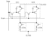
도 6은 앞서 설명한, 발광소자 패키지의 변형예로서, 제1 도전형 반도체층(2131), 활성층(2132) 및 제2 도전형 반도체층(2133)과 같은 에피텍셜층들이 적층된 반도체 적층체(2130)를 포함하고, 제1 도전형 반도체층(2131)에 하나의 제1 전극 패드(2170N)가 접속된 점은 동일하나, 하나의 반도체 발광부(LED23)에 포함된 반도체 적층체(2130)가 제1 도전형 반도체층(2131)을 공유하는 제1 및 제2 영역(LEDa, LEDb)을 가지도록 변형한 예이다. 이에 대응하여 제2 전극 패드(2170P)도 두 개의 제2 전극 패드(2170PA, 2170PB)로 분할된 것을 볼 수 있다. 따라서, 하나의 서브 픽셀(S14)에 독립적으로 구동 가능한 제1 및 제2 영역(LEDa, LEDb)을 갖는 반도체 발광부(LED23)가 배치될 수 있다. 이와 같이, 제1 및 제2 영역(LEDa, LEDb)을 갖는 반도체 발광부(LED23)는, 후술하는 구동 회로를 이용하여, 제1 및 제2 영역(LEDa, LEDb)에 선택적으로 전원을 공급할 수 있다. 따라서, 제1 및 제2 영역(LEDa, LEDb) 중 어느 하나에 문제가 발생하여 정상적으로 동작하지 못할 경우, 그 외의 영역으로 자동적으로 전환됨으로써, 발광소자 패키지의 라이프 타임(life time)을 연장할 수 있는 효과가 있다. 또한, 구동 회로 중 제1 및 제2 영역(LEDa, LEDb) 중 어느 하나를 제어하는 부분에 문제가 발생하였을 때에, 그 이외의 영역을 제어하는 구동 회로로 자동적으로 전환됨으로써 발광소자 패키지의 라이프 타임을 연장할 수도 있다.
FIG. 6 is a modified example of the light-emitting device package described above, which includes a semiconductor laminate (2130) in which epitaxial layers such as a first conductive semiconductor layer (2131), an active layer (2132), and a second conductive semiconductor layer (2133) are laminated, and while the first conductive semiconductor layer (2131) is connected to one first electrode pad (2170N), the semiconductor laminate (2130) included in one semiconductor light-emitting unit (LED23) is modified to have first and second regions (LEDa, LEDb) that share the first conductive semiconductor layer (2131). Correspondingly, it can be seen that the second electrode pad (2170P) is also divided into two second electrode pads (2170PA, 2170PB). Accordingly, a semiconductor light emitting unit (LED23) having first and second regions (LEDa, LEDb) that can be driven independently can be arranged in one sub-pixel (S14). In this way, the semiconductor light emitting unit (LED23) having the first and second regions (LEDa, LEDb) can selectively supply power to the first and second regions (LEDa, LEDb) using a driving circuit described below. Therefore, when a problem occurs in one of the first and second regions (LEDa, LEDb) and cannot operate normally, it is automatically switched to the other region, thereby having the effect of extending the life time of the light emitting element package. In addition, when a problem occurs in a part of the driving circuit that controls one of the first and second regions (LEDa, LEDb), it is also possible to extend the life time of the light emitting element package by automatically switching to the driving circuit that controls the other region.
도 7은 도 6의 발광소자 패키지(LED23)의 구동 회로이다. 하나의 서브 픽셀을 이루는 두개의 영역(LEDa, LEDb)은 각각 별도의 구동 회로(DC1, DC2)에 의해 구동될 수 있다. 두개의 영역(LEDa, LEDb)은 각각 데이터 라인(data)을 통해 데이터 신호를 수용하며, 스캔 라인(scan)을 통해 온/오프 제어될 수 있다. 이러한 구동 회로는 집적 회로 및/또는 박막 트랜지스터 회로를 사용하여 구현될 수 있다.
Fig. 7 is a driving circuit of the light emitting device package (LED23) of Fig. 6. Two regions (LEDa, LEDb) forming one sub-pixel can be driven by separate driving circuits (DC1, DC2), respectively. The two regions (LEDa, LEDb) each receive a data signal through a data line (data) and can be turned on/off controlled through a scan line (scan). Such a driving circuit can be implemented using an integrated circuit and/or a thin film transistor circuit.
이하에서는, 일 실시예에 의한 디스플레이 패널의 제조공정에 대해 설명한다. 도 8 내지 도 16은 도 4의 디스플레이 패널의 주요 제조공정을 개략적으로 설명하기 위한 도면이다.Below, a manufacturing process of a display panel according to one embodiment is described. FIGS. 8 to 16 are drawings for schematically explaining the main manufacturing process of the display panel of FIG. 4.
먼저, 도 8을 참조하면, 성장용 기판(110) 상에 버퍼층(120)을 형성하고, 버퍼층(120) 상에 반도체 적층체(130)를 형성할 수 있다. 성장용 기판(110)은 사파이어, Si, SiC, MgAl2O4, MgO, LiAlO2, LiGaO2, GaN 등의 물질을 포함할 수 있다. 성장용 기판(110)은 후속공정에서 식각 선택성을 확보하기 위해 1019 이상의 농도로 붕소(boron)가 도핑될 수 있다. 반도체 적층체(130)는 유기 금속 화학 증착(Metal Organic Chemical Vapor Deposition, MOCVD), 수소화 기상 에피택시(Hydride Vapor Phase Epitaxy, HVPE), 분자선 에피택시(Molecular Beam Epitaxy, MBE) 등과 같은 공정을 이용하여, 성장용 기판(110) 상에 순차적으로 제1 도전형 반도체층(131), 활성층(132) 및 제2 도전형 반도체층(133)을 성장시킴으로써 형성될 수 있다. 제1 도전형 반도체층(131)과 제2 도전형 반도체층(133)은 각각 n형 반도체층 및 p형 반도체층일 수 있다. 반도체 적층체(130) 상에는 제2 도전형 반도체층(133)의 컨택(contact) 특성을 향상시키기 위한 ITO층(141)이 형성될 수 있다.
First, referring to FIG. 8, a buffer layer (120) may be formed on a growth substrate (110), and a semiconductor laminate (130) may be formed on the buffer layer (120). The growth substrate (110) may include materials such as sapphire, Si, SiC, MgAl2O4 , MgO, LiAlO2 , LiGaO2 , GaN, etc. The growth substrate (110) may be doped with boron at a concentration of 10 19 or more to secure etching selectivity in a subsequent process. The semiconductor laminate (130) can be formed by sequentially growing a first conductive semiconductor layer (131), an active layer (132), and a second conductive semiconductor layer (133) on a growth substrate (110) using a process such as metal organic chemical vapor deposition (MOCVD), hydride vapor phase epitaxy (HVPE), molecular beam epitaxy (MBE), etc. The first conductive semiconductor layer (131) and the second conductive semiconductor layer (133) can be an n-type semiconductor layer and a p-type semiconductor layer, respectively. An ITO layer (141) can be formed on the semiconductor laminate (130) to improve the contact characteristics of the second conductive semiconductor layer (133).
도 9를 참조하면, 제1 도전형 반도체층(131)의 적어도 일부가 노출되도록 반도체 적층체(130)의 일부영역(E)을 식각하여 메사영역(M)을 형성할 수 있다.
Referring to FIG. 9, a part of a region (E) of a semiconductor laminate (130) may be etched to form a mesa region (M) so that at least a part of the first challenge type semiconductor layer (131) is exposed.
도 10 및 도 11을 참조하면, 반도체 적층체(130)의 상부면을 덮도록 절연층(142)을 형성하고, 일부 영역을 제거하여 제1 도전형 반도체층(131) 및 제2 도전형 반도체층(133)이 각각 저면에 노출되는 컨택홀(H1, H2)을 형성하고, 컨택홀(H1, H2)에 제1 및 제2 전극(150N, 150P)을 형성할 수 있다.
Referring to FIGS. 10 and 11, an insulating layer (142) is formed to cover the upper surface of the semiconductor laminate (130), a portion of the area is removed to form contact holes (H1, H2) in which the first conductive semiconductor layer (131) and the second conductive semiconductor layer (133) are exposed on the lower surface, respectively, and first and second electrodes (150N, 150P) can be formed in the contact holes (H1, H2).
도 12를 참조하면, 반도체 적층체(130)를 제1 내지 제3 반도체 발광부(LED1, LED2, LED3)로 분리하는 트렌치(T)를 형성할 수 있다. 트렌치(T)는 반도체 적층체(130) 뿐만 아니라 성장용 기판(110)의 일부 영역을 소정의 깊이(D)로 식각할 수 있다. 이러한, 트렌치(T)에는 후속공정에서 몰딩부가 충전되어 파장변환부를 분리하는 격벽 구조가 형성될 수 있다.
Referring to FIG. 12, a trench (T) can be formed to separate the semiconductor laminate (130) into first to third semiconductor light-emitting parts (LED1, LED2, LED3). The trench (T) can etch not only the semiconductor laminate (130) but also a portion of the growth substrate (110) to a predetermined depth (D). In the trench (T), a molding part can be filled in a subsequent process to form a partition structure that separates the wavelength conversion part.
도 13을 참조하면, 제1 내지 제3 반도체 발광부(LED1, LED2, LED3)를 덮는 절연층(161) 및 절연층(161)을 덮는 반사층(162)을 형성할 수 있다.
Referring to FIG. 13, an insulating layer (161) covering the first to third semiconductor light-emitting units (LED1, LED2, LED3) and a reflective layer (162) covering the insulating layer (161) can be formed.
도 14를 참조하면, 제1 및 제2 전극(150N, 150P)에 도금층을 형성하여 제1 및 제2 전극 패드(170N, 170P)를 형성하고, 제1 및 제2 전극 패드(170N, 170P)의 측면을 덮는 몰딩부(180)를 형성할 수 있다. 몰딩부(180)는 트렌치(T)를 채워 제1 내지 제3 반도체 발광부(LED1, LED2, LED3)를 서로 격리할 수 있다. 몰딩부(180)는 플렉시블(flexible)한 특성을 갖도록 낮은 모듈러스(modulus)를 갖는 물질로 이루어질 수 있으며, 특히, 반도체 적층체(130) 보다 낮은 모듈러스를 가지며 높은 인장특성을 갖는 물질로 이루어 질 수 있다. 예를 들어, 몰딩부(180)는 폴리이미드(polyimide, PI), 폴리사이클로핵실렌디메틸렌 테레프탈레이트(polycyclohexylenedimethylene terephthalate, PCT) 및 에폭시 몰딩 컴파운드(epoxy molding compound, EMC) 중 하나를 포함하는 물질로 이루어질 수 있다.
Referring to FIG. 14, a plating layer may be formed on the first and second electrodes (150N, 150P) to form first and second electrode pads (170N, 170P), and a molding part (180) covering side surfaces of the first and second electrode pads (170N, 170P) may be formed. The molding part (180) may fill the trench (T) to isolate the first to third semiconductor light-emitting parts (LED1, LED2, LED3) from each other. The molding part (180) may be made of a material having a low modulus so as to have flexible characteristics, and in particular, may be made of a material having a lower modulus than the semiconductor laminate (130) and high tensile characteristics. For example, the molding portion (180) may be made of a material including one of polyimide (PI), polycyclohexylenedimethylene terephthalate (PCT), and epoxy molding compound (EMC).
도 15를 참조하면, 몰딩부(180)의 하부에 본딩층(200)을 개재하여 제2 기판 구조물(300)을 부착시킬 수 있다. 제2 기판 구조물(300)은 제1 내지 제3 반도체 발광부(LED1, LED2, LED3)를 제어하기 위한 복수의 TFT 셀을 포함하는 구동 회로(driving circuit)를 포함할 수 있다. 복수의 TFT 셀은 반도체 기판에 불순물을 주입하여 형성된 반도체층을 포함할 수 있다. 예를 들어, 복수의 TFT 셀을 구성하는 반도체층은 폴리실리콘과 실리콘계 반도체, 인듐 갈륨 산화아연과 같은 반도체 산화물 또는 실리콘 저마늄과 같은 화합물 반도체를 포함할 수 있다. 반도체 기판은 성장용 기판(110)을 분리하는 후속 공정에서 식각 선택성을 확보하기 위해, 성장용 기판(110)에 도핑된 농도보다 저 농도인 1016 이하의 농도로 붕소가 도핑될 수 있다.
Referring to FIG. 15, a second substrate structure (300) may be attached to a lower portion of a molding portion (180) by interposing a bonding layer (200). The second substrate structure (300) may include a driving circuit including a plurality of TFT cells for controlling the first to third semiconductor light-emitting portions (LED1, LED2, LED3). The plurality of TFT cells may include a semiconductor layer formed by injecting an impurity into a semiconductor substrate. For example, the semiconductor layer constituting the plurality of TFT cells may include polysilicon and a silicon-based semiconductor, a semiconductor oxide such as indium gallium zinc oxide, or a compound semiconductor such as silicon germanium. In order to secure etching selectivity in a subsequent process of separating the growth substrate (110), the semiconductor substrate may be doped with boron at a concentration of 10 16 or less, which is lower than the concentration doped in the growth substrate (110).
도 16을 참조하면, 제1 내지 제3 반도체 발광부(LED1, LED2, LED3)에서 성장용 기판(110)을 분리하여, 상부에서 보았을 때 격벽 구조에 의해 정의 홈부(H5R, H5G, H5B)를 형성할 수 있다. 계속하여, 양자점(Quantum Dot, QD)과 같은 파장변환물질을 액상의 바인더 수지에 분산된 상태로 홈부(H5R, H5G, H5B)에 충전하여 파장변환부(190R, 190G, 190B)를 형성하고, 상부에 보호층(400)을 부착하면 도 4의 디스플레이 패널(1)을 제조할 수 있다.
Referring to FIG. 16, by separating the growth substrate (110) from the first to third semiconductor light-emitting units (LED1, LED2, LED3), a groove portion (H5R, H5G, H5B) defined by a partition structure can be formed when viewed from above. Subsequently, a wavelength conversion material such as a quantum dot (QD) is dispersed in a liquid binder resin and filled into the groove portion (H5R, H5G, H5B) to form a wavelength conversion unit (190R, 190G, 190B), and a protective layer (400) is attached thereto, thereby manufacturing the display panel (1) of FIG. 4.
일 실시예에 의한 디스플레이 패널의 제조공정에 대해 설명한다. 도 17 내지 도 21는 도 5의 디스플레이 패널의 주요 제조공정을 개략적으로 설명하기 위한 도면이다. 도 17의 이전 공정은 앞서 설명한 실시예의 도 12까지의 공정과 동일하므로 생략한다.
A manufacturing process of a display panel according to one embodiment is described. FIGS. 17 to 21 are drawings for schematically explaining the main manufacturing processes of the display panel of FIG. 5. The process before FIG. 17 is the same as the process up to FIG. 12 of the previously described embodiment, and therefore is omitted.
도 17을 참조하면, 제1 및 제2 전극(1150N, 1150P)에 도금층을 형성하여 제1 및 제2 전극 패드(1170N, 1170P)를 형성할 수 있다.
Referring to FIG. 17, a plating layer can be formed on the first and second electrodes (1150N, 1150P) to form first and second electrode pads (1170N, 1170P).
도 18을 참조하면, 제1 및 제2 전극 패드(1170N, 1170P)의 측면을 덮는 제1 몰딩부(1161)를 형성할 수 있다. 제1 몰딩부(1161)는 트렌치(T)를 채워 제1 내지 제3 반도체 발광부(LED11, LED12, LED13)를 서로 격리할 수 있다. 제1 몰딩부(1161)는 플렉시블(flexible)한 특성을 갖도록 낮은 모듈러스(modulus)를 갖는 물질로 이루어질 수 있으며, 특히, 반도체 적층체(1130) 보다 낮은 모듈러스를 가지며 높은 인장특성을 갖는 물질로 이루어 질 수 있다. 예를 들어, 제1 몰딩부(1161)는 PCT 및 white EMC 중 하나를 포함하는 물질로 이루어질 수 있다. PCT 및 white EMC는 앞서 설명한 실시예에서 몰딩부로 채용가능한 물질인 PI에 비하여, 반사도가 우수하므로, 제1 내지 제3 반도체 발광부(LED11, LED12, LED13)에서 방출된 빛을 반사하기 위한 별도의 반사층을 형성하는 단계를 생략할 수 있다.
Referring to FIG. 18, a first molding portion (1161) covering side surfaces of the first and second electrode pads (1170N, 1170P) can be formed. The first molding portion (1161) can fill a trench (T) to isolate the first to third semiconductor light-emitting portions (LED11, LED12, LED13) from each other. The first molding portion (1161) can be made of a material having a low modulus so as to have a flexible characteristic, and in particular, can be made of a material having a lower modulus than the semiconductor laminate (1130) and a high tensile characteristic. For example, the first molding portion (1161) can be made of a material including one of PCT and white EMC. Since PCT and white EMC have superior reflectivity compared to PI, which is a material that can be employed as a molding part in the above-described embodiment, the step of forming a separate reflective layer for reflecting light emitted from the first to third semiconductor light-emitting parts (LED11, LED12, LED13) can be omitted.
도 19를 참조하면, 제1 몰딩부(1161) 상에 PI를 포함하는 물질로 이루어진 제2 몰딩부(1180)를 형성할 수 있다. PCT 및 white EMC 중 하나를 포함하는 물질로 이루어진 제1 몰딩부(1161)는 녹는점이 230℃ 이하이므로, 350℃ 이상의 온도에서 본딩이 이루어지는 후속 공정에서 녹아 몰딩의 기능을 상실할 수 있다. 따라서, PCT 및 white EMC로 이루어진 제1 몰딩부(1161) 상에, PCT 및 white EMC에 비해 녹는점이 높은 PI로 이루어진 제2 몰딩부(1180)는 형성하면, 본딩 공정의 열에 의해 제1 몰딩부(1161)가 녹더라도 제2 몰딩부(1180)에 의해 외형이 유지될 수 있다.
Referring to FIG. 19, a second molding part (1180) made of a material including PI can be formed on the first molding part (1161). Since the first molding part (1161) made of a material including one of PCT and white EMC has a melting point of 230° C. or lower, it may melt and lose the molding function in a subsequent process in which bonding is performed at a temperature of 350° C. or higher. Therefore, if the second molding part (1180) made of PI having a higher melting point than PCT and white EMC is formed on the first molding part (1161) made of PCT and white EMC, even if the first molding part (1161) melts due to the heat of the bonding process, the outer shape can be maintained by the second molding part (1180).
도 20을 참조하면, 제2 몰딩부(1180)의 하부에 본딩층(1200)을 개재하여 제2 기판 구조물(1300)을 부착시킬 수 있다. 제2 기판 구조물(1300)은 제1 내지 제3 반도체 발광부(LED11, LED12, LED13)를 제어하기 위한 복수의 TFT 셀을 포함하는 구동 회로(driving circuit)를 포함할 수 있다.
Referring to FIG. 20, a second substrate structure (1300) may be attached by interposing a bonding layer (1200) on the lower portion of the second molding portion (1180). The second substrate structure (1300) may include a driving circuit including a plurality of TFT cells for controlling the first to third semiconductor light-emitting portions (LED11, LED12, LED13).
도 21을 참조하면, 제1 내지 제3 반도체 발광부(LED11, LED12, LED13)에서 성장용 기판(1110)을 분리하여, 상부에서 보았을 때 격벽 구조에 의해 정의 홈부(H6R, H6G, H6B)를 형성할 수 있다. 계속하여, 양자점(Quantum Dot, QD)과 같은 파장변환물질을 액상의 바인더 수지에 분산된 상태로 홈부(H6R, H6G, H6B)에 충전하여 파장변환부(1190R, 1190G, 1190B)를 형성하고, 상부에 보호층(1400)을 부착하면 도 5의 디스플레이 패널(2)을 제조할 수 있다.
Referring to FIG. 21, by separating the growth substrate (1110) from the first to third semiconductor light-emitting units (LED11, LED12, LED13), a groove portion (H6R, H6G, H6B) defined by a partition structure can be formed when viewed from above. Subsequently, a wavelength conversion material such as a quantum dot (QD) is dispersed in a liquid binder resin and filled into the groove portion (H6R, H6G, H6B) to form a wavelength conversion unit (1190R, 1190G, 1190B), and a protective layer (1400) is attached thereto, thereby manufacturing the display panel (2) of FIG. 5.
이상, 첨부된 도면을 참조하여 본 발명의 실시 예를 설명하였지만, 본 발명이 속하는 기술분야에서 통상의 지식을 가진 자는 본 발명이 그 기술적 사상이나 필수적인 특징을 변경하지 않고서 다른 구체적인 형태로 실시될 수 있다는 것을 이해할 수 있을 것이다. 그러므로 이상에서 기술한 실시 예에는 모든 면에서 예시적인 것이며 한정적이 아닌 것으로 이해해야만 한다.
Above, while the embodiments of the present invention have been described with reference to the attached drawings, those skilled in the art to which the present invention pertains will understand that the present invention can be implemented in other specific forms without changing the technical idea or essential features thereof. Therefore, it should be understood that the embodiments described above are exemplary in all respects and not restrictive.
100: 제1 기판 구조물
200: 본딩층
300: 제2 기판 구조물
400: 보호층100: First substrate structure
200: Bonding layer
300: Second substrate structure
400: Protective layer
Claims (20)
상기 반도체 적층체를 관통하도록 상기 제1 면 방향에서 식각하여 상기 성장용 기판에 소정 깊이의 트렌치를 형성함으로써, 상기 반도체 적층체를 서로 분리된 복수의 반도체 발광부로 분리하는 단계;
상기 복수의 반도체 발광부를 덮도록 유연성 있는 절연물질을 도포하여 상기 복수의 반도체 발광부를 서로 절연하며 상기 트렌치를 채우는 몰딩부를 형성하는 단계;
상기 성장용 기판을 제거하여, 상기 몰딩부에 의해 서로 분리되며 상기 복수의 반도체 발광부에 각각 대응되는 복수의 홈부를 형성하는 단계; 및
상기 복수의 홈부에 복수의 파장변환부를 형성하는 단계;를 포함하고,
상기 몰딩부는 상기 복수의 파장변환부의 측면 및 상기 복수의 반도체 발광부의 측면을 일체로 둘러싸도록 형성되는 제1 몰딩부, 및 상기 제1 몰딩부의 하면 상에 형성되는 제2 몰딩부를 포함하고,
상기 제1 몰딩부는 폴리사이클로핵실렌디메틸렌 테레프탈레이트(polycyclohexylenedimethylene terephthalate, PCT) 및 백색 에폭시 몰딩 컴파운드(white epoxy molding compound, white EMC) 중 적어도 하나를 포함하고,
상기 제2 몰딩부는 폴리이미드(polyimide, PI)를 포함하는 발광소자 패키지 제조방법.
A step of forming a semiconductor laminate having a first conductive semiconductor layer, an active layer, and a second conductive semiconductor layer on a first surface of a growth substrate having a first surface and a second surface opposite to the first surface;
A step of forming a trench of a predetermined depth in the growth substrate by etching in the first surface direction so as to penetrate the semiconductor laminate, thereby separating the semiconductor laminate into a plurality of semiconductor light-emitting portions separated from each other;
A step of forming a molding part that fills the trench and insulates the plurality of semiconductor light-emitting parts from each other by applying a flexible insulating material to cover the plurality of semiconductor light-emitting parts;
A step of removing the growth substrate, forming a plurality of grooves separated from each other by the molding part and each corresponding to the plurality of semiconductor light-emitting parts; and
A step of forming a plurality of wavelength conversion parts in the plurality of home parts;
The molding part includes a first molding part formed to integrally surround the side surfaces of the plurality of wavelength conversion parts and the side surfaces of the plurality of semiconductor light-emitting parts, and a second molding part formed on the lower surface of the first molding part.
The first molding part comprises at least one of polycyclohexylenedimethylene terephthalate (PCT) and a white epoxy molding compound (white EMC).
A method for manufacturing a light-emitting device package, wherein the second molding part includes polyimide (PI).
상기 유연성 있는 절연물질은 상기 반도체 적층체 보다 낮은 모듈러스(modulus)를 갖는 물질인 발광소자 패키지 제조방법.
In the first paragraph,
A method for manufacturing a light emitting device package, wherein the flexible insulating material has a lower modulus than the semiconductor laminate.
상기 복수의 반도체 발광부 및 복수의 파장변환부는 각각 대응하여 복수의 서브 픽셀을 이루며, 상기 복수의 서브 픽셀을 포함하는 하나의 픽셀은, 8000PPI(pixel per inch) 이상의 화소밀도를 갖는 발광소자 패키지 제조방법.
In the first paragraph,
A method for manufacturing a light-emitting device package, wherein the plurality of semiconductor light-emitting units and the plurality of wavelength conversion units respectively correspond to each other and form a plurality of sub-pixels, and one pixel including the plurality of sub-pixels has a pixel density of 8000 PPI (pixel per inch) or more.
상기 반도체 적층체를 형성하는 단계는,
상기 제2 도전형 반도체층 상에 ITO층과 절연층을 순차적으로 적층하는 단계를 더 포함하는 발광소자 패키지 제조방법.
In the first paragraph,
The step of forming the semiconductor laminate is:
A method for manufacturing a light-emitting device package further comprising the step of sequentially laminating an ITO layer and an insulating layer on the second challenge-type semiconductor layer.
상기 제2 몰딩부는 상기 제1 몰딩부보다 높은 녹는 점을 갖는 물질로 이루어진 발광소자 패키지 제조방법.
In the first paragraph,
A method for manufacturing a light emitting device package, wherein the second molding part is made of a material having a higher melting point than the first molding part.
상기 반도체 적층체를 서로 분리된 복수의 반도체 발광부로 분리하는 단계 전에, 상기 제2 도전형 반도체층 상에 ITO층을 형성하는 단계; 및
상기 ITO층 상에 절연층을 형성하는 단계;를 더 포함하는 발광소자 패키지 제조방법.
In the first paragraph,
Before the step of separating the semiconductor laminate into a plurality of semiconductor light-emitting parts separated from each other, a step of forming an ITO layer on the second conductive semiconductor layer; and
A method for manufacturing a light-emitting device package, further comprising: forming an insulating layer on the ITO layer.
제2 기판 상에 상기 복수의 반도체 발광부에 각각 대응되도록 배치된 복수의 TFT셀을 포함하는 제2 기판 구조물을 마련하는 단계;
상기 제1 기판 구조물의 상기 전극 패드들과 상기 제2 기판 구조물의 접속부들이 각각 대응되도록, 상기 제1 기판 구조물과 상기 제2 기판 구조물을 접합하는 단계;
상기 제1 기판을 제거하여 상기 몰딩부에 의해 분리되며 상기 복수의 반도체 발광부에 각각 대응되는 복수의 홈부를 형성하는 단계; 및
상기 복수의 홈부에 각각 복수의 파장변환부를 형성하는 단계;를 포함하며, 상기 몰딩부는 상기 반도체 발광부보다 보다 낮은 모듈러스(modulus)를 갖는 물질로 이루어지고,
상기 제1 기판 및 상기 제2 기판은 반도체 기판으로 이루어지며,
상기 제1 기판과 상기 제2 기판은 서로 상이한 식각 선택비를 갖는 디스플레이 패널 제조방법.
A step for providing a first substrate structure having a plurality of semiconductor light-emitting portions, each having a first conductive semiconductor layer, an active layer, and a second conductive semiconductor layer on a first substrate, electrode pads respectively connected to the first conductive semiconductor layers and the second conductive semiconductor layers of the plurality of semiconductor light-emitting portions, and a molding portion made of a flexible material and covering the plurality of semiconductor light-emitting portions;
A step of providing a second substrate structure including a plurality of TFT cells arranged to correspond to the plurality of semiconductor light-emitting units on a second substrate;
A step of bonding the first substrate structure and the second substrate structure so that the electrode pads of the first substrate structure and the connecting portions of the second substrate structure correspond to each other;
A step of removing the first substrate and forming a plurality of grooves each corresponding to the plurality of semiconductor light-emitting parts, separated by the molding part; and
A step of forming a plurality of wavelength conversion parts in each of the plurality of grooves; wherein the molding part is made of a material having a lower modulus than the semiconductor light-emitting part,
The above first substrate and the above second substrate are made of semiconductor substrates,
A method for manufacturing a display panel, wherein the first substrate and the second substrate have different etching selectivities.
상기 제1 기판은 상기 제2 기판 보다 높은 농도로 붕소(boron)가 도핑되는 디스플레이 패널 제조방법.
In Article 12,
A method for manufacturing a display panel, wherein the first substrate is doped with boron at a higher concentration than the second substrate.
상기 복수의 반도체 발광부는 실질적으로 동일한 파장의 광을 방출하도록 구성된 디스플레이 패널 제조방법.
In Article 12,
A method for manufacturing a display panel, wherein the plurality of semiconductor light-emitting units are configured to emit light of substantially the same wavelength.
상기 복수의 반도체 발광부는 실질적으로 서로 동일한 면적을 갖도록 형성되는 디스플레이 패널 제조방법.
In Article 12,
A method for manufacturing a display panel, wherein the plurality of semiconductor light-emitting units are formed to have substantially the same area.
상기 복수의 반도체 발광부 및 복수의 파장변환부는 각각 대응하여 복수의 서브 픽셀을 이루며, 상기 복수의 서브 픽셀을 포함하는 하나의 픽셀은, 8000PPI(pixel per inch) 이상의 밀도를 갖는 디스플레이 패널 제조방법.
In Article 12,
A method for manufacturing a display panel in which the plurality of semiconductor light-emitting units and the plurality of wavelength conversion units respectively correspond to each other and form a plurality of sub-pixels, and one pixel including the plurality of sub-pixels has a density of 8000 PPI (pixel per inch) or more.
상기 복수의 반도체 발광부는 각각 서로 분할된 복수의 제2 도전형 반도체층을 포함하며, 상기 복수의 제2 도전형 반도체층은 상기 제1 도전형 반도체층을 공유하는 디스플레이 패널 제조방법.
In Article 12,
A method for manufacturing a display panel, wherein the plurality of semiconductor light-emitting sections each include a plurality of second conductive semiconductor layers that are separated from each other, and the plurality of second conductive semiconductor layers share the first conductive semiconductor layer.
상기 복수의 제2 도전형 반도체층은 각각의 전극 패드들에 의해 선택적으로 전원이 인가되는 디스플레이 패널 제조방법.
In Article 18,
A method for manufacturing a display panel in which the plurality of second conductive semiconductor layers are selectively powered by respective electrode pads.
상기 몰딩부는,
상기 복수의 반도체 발광부를 덮는 제1 몰딩부; 및
상기 제1 몰딩부를 덮으며, 상기 제1 몰딩부 보다 높은 녹는점을 갖는 물질로 형성된 제2 몰딩부;를 포함하며,
상기 제2 몰딩부의 녹는점은 상기 제1 기판 구조물과 상기 제2 기판 구조물을 접합하는 단계의 공정온도보다 높은 디스플레이 패널 제조방법.
In Article 12,
The above molding part,
A first molding part covering the plurality of semiconductor light-emitting parts; and
A second molding part covering the first molding part and formed of a material having a higher melting point than the first molding part;
A method for manufacturing a display panel, wherein the melting point of the second molding portion is higher than the process temperature of the step of bonding the first substrate structure and the second substrate structure.
Priority Applications (4)
| Application Number | Priority Date | Filing Date | Title |
|---|---|---|---|
| KR1020190081599A KR102780352B1 (en) | 2019-07-05 | 2019-07-05 | Method of manufacturing light emitting device package and method of manufacturing display panel using the same |
| US16/716,752 US12336346B2 (en) | 2019-07-05 | 2019-12-17 | Method of manufacturing light emitting device package and method of manufacturing display panel using the same |
| DE102020108077.8A DE102020108077A1 (en) | 2019-07-05 | 2020-03-24 | METHOD OF MANUFACTURING A LIGHTING DEVICE PACKAGE AND METHOD OF MANUFACTURING A DISPLAY PANEL USING THE SAME |
| CN202010627430.1A CN112186078B (en) | 2019-07-05 | 2020-07-02 | Method for manufacturing light emitting device package and method for manufacturing display panel using the same |
Applications Claiming Priority (1)
| Application Number | Priority Date | Filing Date | Title |
|---|---|---|---|
| KR1020190081599A KR102780352B1 (en) | 2019-07-05 | 2019-07-05 | Method of manufacturing light emitting device package and method of manufacturing display panel using the same |
Publications (2)
| Publication Number | Publication Date |
|---|---|
| KR20210005454A KR20210005454A (en) | 2021-01-14 |
| KR102780352B1 true KR102780352B1 (en) | 2025-03-12 |
Family
ID=73919649
Family Applications (1)
| Application Number | Title | Priority Date | Filing Date |
|---|---|---|---|
| KR1020190081599A Active KR102780352B1 (en) | 2019-07-05 | 2019-07-05 | Method of manufacturing light emitting device package and method of manufacturing display panel using the same |
Country Status (4)
| Country | Link |
|---|---|
| US (1) | US12336346B2 (en) |
| KR (1) | KR102780352B1 (en) |
| CN (1) | CN112186078B (en) |
| DE (1) | DE102020108077A1 (en) |
Families Citing this family (17)
| Publication number | Priority date | Publication date | Assignee | Title |
|---|---|---|---|---|
| KR102884889B1 (en) | 2020-01-30 | 2025-11-11 | 삼성전자주식회사 | Light-emitting element package |
| KR102888284B1 (en) * | 2020-02-20 | 2025-11-19 | 엘지전자 주식회사 | Display device using semi-conductor light emitting devices |
| US11842989B2 (en) * | 2020-03-10 | 2023-12-12 | Meta Platforms Technologies, Llc | Integrating control circuits with light emissive circuits with dissimilar wafer sizes |
| GB2593699B (en) * | 2020-03-30 | 2022-10-26 | Plessey Semiconductors Ltd | Monolithic LED pixel |
| FR3112902B1 (en) * | 2020-07-22 | 2022-12-16 | Aledia | Flexible optoelectronic device and method of making same |
| CN112885932B (en) * | 2021-01-19 | 2023-07-04 | 江西锐芯微电子科技有限公司 | A kind of manufacturing method of micro-LED display chip |
| CN113097367A (en) * | 2021-03-24 | 2021-07-09 | 深圳市华星光电半导体显示技术有限公司 | QD-miniLED display panel and preparation method thereof |
| KR20220149857A (en) | 2021-04-30 | 2022-11-09 | 삼성디스플레이 주식회사 | Display device |
| EP4266388A4 (en) * | 2021-06-30 | 2024-07-31 | Samsung Electronics Co., Ltd. | INORGANIC LIGHT-EMITTING DIODE AND METHOD FOR MANUFACTURING SAME |
| TWI818318B (en) * | 2021-09-24 | 2023-10-11 | 光鋐科技股份有限公司 | Light-emitting diode chip and method for manufacturing the same |
| KR20230053028A (en) | 2021-10-13 | 2023-04-21 | 삼성디스플레이 주식회사 | Display device, method for driving the same |
| JP2025502263A (en) * | 2022-01-13 | 2025-01-24 | 昭栄化学工業株式会社 | Light emitting diode and method for its manufacture by selective growth of active layer from trench bounded region - Patents.com |
| KR20230113472A (en) | 2022-01-21 | 2023-07-31 | 삼성디스플레이 주식회사 | Display device and tiled display device |
| CN114709319B (en) * | 2022-04-11 | 2023-07-11 | 东莞市中麒光电技术有限公司 | Color conversion structure manufacturing method, color conversion structure, crystal grain manufacturing method and crystal grain |
| TWI807909B (en) * | 2022-07-08 | 2023-07-01 | 宏齊科技股份有限公司 | Wafer-level full-color display device and manufacturing thereof |
| EP4627628A1 (en) * | 2022-12-01 | 2025-10-08 | Samsung Electronics Co., Ltd. | Display including lateral-structure multicolor light emitting device pixels and method of fabrication thereof |
| WO2025086297A1 (en) * | 2023-10-27 | 2025-05-01 | 京东方科技集团股份有限公司 | Display substrate and manufacturing method therefor, and display device |
Family Cites Families (56)
| Publication number | Priority date | Publication date | Assignee | Title |
|---|---|---|---|---|
| EP0858110B1 (en) | 1996-08-27 | 2006-12-13 | Seiko Epson Corporation | Separating method, method for transferring thin film device, and liquid crystal display device manufactured by using the transferring method |
| USRE38466E1 (en) | 1996-11-12 | 2004-03-16 | Seiko Epson Corporation | Manufacturing method of active matrix substrate, active matrix substrate and liquid crystal display device |
| US7208725B2 (en) | 1998-11-25 | 2007-04-24 | Rohm And Haas Electronic Materials Llc | Optoelectronic component with encapsulant |
| JP3906654B2 (en) | 2000-07-18 | 2007-04-18 | ソニー株式会社 | Semiconductor light emitting device and semiconductor light emitting device |
| CN1241272C (en) | 2001-08-22 | 2006-02-08 | 索尼公司 | Nitride semiconductor element and production method for thereof |
| JP2003218034A (en) | 2002-01-17 | 2003-07-31 | Sony Corp | Selective growth method, semiconductor light emitting device and method of manufacturing the same |
| JP3815335B2 (en) | 2002-01-18 | 2006-08-30 | ソニー株式会社 | Semiconductor light emitting device and manufacturing method thereof |
| KR100499129B1 (en) | 2002-09-02 | 2005-07-04 | 삼성전기주식회사 | Light emitting laser diode and fabricatin method thereof |
| US7002182B2 (en) | 2002-09-06 | 2006-02-21 | Sony Corporation | Semiconductor light emitting device integral type semiconductor light emitting unit image display unit and illuminating unit |
| KR100714639B1 (en) | 2003-10-21 | 2007-05-07 | 삼성전기주식회사 | Light emitting element |
| KR100506740B1 (en) | 2003-12-23 | 2005-08-08 | 삼성전기주식회사 | Nitride semiconductor light emitting device and method of manufacturing the same |
| KR100664985B1 (en) | 2004-10-26 | 2007-01-09 | 삼성전기주식회사 | Nitride-based semiconductor device |
| EP1724844A2 (en) * | 2005-05-20 | 2006-11-22 | Semiconductor Energy Laboratory Co., Ltd. | Photoelectric conversion device, manufacturing method thereof and semiconductor device |
| KR100665222B1 (en) | 2005-07-26 | 2007-01-09 | 삼성전기주식회사 | LED package using diffusion material and manufacturing method thereof |
| KR100661614B1 (en) | 2005-10-07 | 2006-12-26 | 삼성전기주식회사 | Nitride-based semiconductor light emitting device and its manufacturing method |
| TWI294749B (en) | 2005-12-29 | 2008-03-11 | Ind Tech Res Inst | Display device and method for fabricating display device |
| KR100723247B1 (en) | 2006-01-10 | 2007-05-29 | 삼성전기주식회사 | Chip coated LED package and manufacturing method thereof |
| KR100735325B1 (en) | 2006-04-17 | 2007-07-04 | 삼성전기주식회사 | Light emitting diode package and its manufacturing method |
| KR100930171B1 (en) | 2006-12-05 | 2009-12-07 | 삼성전기주식회사 | White light emitting device and white light source module using same |
| KR100855065B1 (en) | 2007-04-24 | 2008-08-29 | 삼성전기주식회사 | Light emitting diode package |
| KR100982980B1 (en) | 2007-05-15 | 2010-09-17 | 삼성엘이디 주식회사 | Surface light source device and LCD backlight unit having same |
| KR101164026B1 (en) | 2007-07-12 | 2012-07-18 | 삼성전자주식회사 | Nitride semiconductor light emitting device and fabrication method thereof |
| KR100891761B1 (en) | 2007-10-19 | 2009-04-07 | 삼성전기주식회사 | Semiconductor light emitting device, manufacturing method thereof and semiconductor light emitting device package using same |
| KR101332794B1 (en) | 2008-08-05 | 2013-11-25 | 삼성전자주식회사 | Light emitting device, light emitting system comprising the same, and fabricating method of the light emitting device and the light emitting system |
| KR20100030470A (en) | 2008-09-10 | 2010-03-18 | 삼성전자주식회사 | Light emitting device and system providing white light with various color temperatures |
| KR101530876B1 (en) | 2008-09-16 | 2015-06-23 | 삼성전자 주식회사 | Light emitting element with increased light emitting amount, light emitting device comprising the same, and fabricating method of the light emitting element and the light emitting device |
| US8008683B2 (en) | 2008-10-22 | 2011-08-30 | Samsung Led Co., Ltd. | Semiconductor light emitting device |
| US9213181B2 (en) | 2011-05-20 | 2015-12-15 | Pixtronix, Inc. | MEMS anchor and spacer structure |
| US8796665B2 (en) | 2011-08-26 | 2014-08-05 | Micron Technology, Inc. | Solid state radiation transducers and methods of manufacturing |
| DE102011056888A1 (en) | 2011-12-22 | 2013-06-27 | Osram Opto Semiconductors Gmbh | Display device and method for producing a display device |
| US9178123B2 (en) | 2012-12-10 | 2015-11-03 | LuxVue Technology Corporation | Light emitting device reflective bank structure |
| US20140267281A1 (en) * | 2013-03-13 | 2014-09-18 | Ericom Software Ltd. | Method for displaying a remote desktop on a portable touch screen device |
| KR20150069228A (en) * | 2013-12-13 | 2015-06-23 | 서울바이오시스 주식회사 | Light emitting diode with wavelength conversion layer and method of fabricating the same |
| KR101660020B1 (en) * | 2015-08-21 | 2016-09-30 | 서울반도체 주식회사 | Wafer-level light emitting diode package and method of fabricating the same |
| GB2544728B (en) | 2015-11-17 | 2020-08-19 | Facebook Tech Llc | Redundancy in inorganic light emitting diode displays |
| JP6851166B2 (en) * | 2015-10-12 | 2021-03-31 | 株式会社半導体エネルギー研究所 | Manufacturing method of semiconductor device |
| KR102524805B1 (en) | 2016-02-12 | 2023-04-25 | 삼성전자주식회사 | Lighting source module, display panel and display apparatus |
| KR102263041B1 (en) | 2016-02-26 | 2021-06-09 | 삼성전자주식회사 | Light emitting diode(LED) device for implementing multi-colors |
| KR20170129983A (en) * | 2016-05-17 | 2017-11-28 | 삼성전자주식회사 | Led lighting device package, display apparatus using the same and method of manufacuring process the same |
| US10037981B2 (en) * | 2016-05-18 | 2018-07-31 | Globalfoundries Inc. | Integrated display system with multi-color light emitting diodes (LEDs) |
| KR102553630B1 (en) * | 2016-08-11 | 2023-07-10 | 삼성전자주식회사 | Led lighting device package and display apparatus using the same |
| JP2018063399A (en) | 2016-10-14 | 2018-04-19 | 株式会社半導体エネルギー研究所 | Display device, and method for driving display device |
| KR102650341B1 (en) | 2016-11-25 | 2024-03-22 | 엘지전자 주식회사 | Display device using semiconductor light emitting device and method for manufacturing |
| KR102611980B1 (en) * | 2016-12-14 | 2023-12-08 | 삼성전자주식회사 | Light emitting diode(LED) device for implementing multi-colors |
| KR102652087B1 (en) * | 2016-12-16 | 2024-03-28 | 삼성전자주식회사 | Semiconductor light emitting device |
| KR20180078940A (en) | 2016-12-30 | 2018-07-10 | (재)한국나노기술원 | Light emitting diode chip and manufacturing method thereof |
| WO2018169968A1 (en) * | 2017-03-16 | 2018-09-20 | Invensas Corporation | Direct-bonded led arrays and applications |
| KR102422386B1 (en) | 2017-04-21 | 2022-07-20 | 주식회사 루멘스 | Micro led display apparatus and method for fabricating the same |
| CN107359175B (en) | 2017-07-25 | 2020-02-11 | 上海天马微电子有限公司 | Micro light-emitting diode display panel and display device |
| EP3662514B1 (en) * | 2017-08-03 | 2024-07-17 | CreeLED, Inc. | High density pixelated-led chips |
| US11263933B2 (en) * | 2017-10-25 | 2022-03-01 | Samsung Electronics Co., Ltd. | LED panel and display apparatus having the same |
| KR102421729B1 (en) * | 2017-12-14 | 2022-07-15 | 삼성전자주식회사 | Led lighting device package and display apparatus using the same |
| US10566317B2 (en) * | 2018-05-20 | 2020-02-18 | Black Peak LLC | Light emitting device with small size and large density |
| KR20190137458A (en) * | 2018-06-01 | 2019-12-11 | 삼성전자주식회사 | Method of display module using light emitting diode |
| KR102039838B1 (en) * | 2018-10-19 | 2019-11-27 | 한국광기술원 | Micro led display pixel assembly and method for manufacturing the same |
| KR102746084B1 (en) * | 2019-07-08 | 2024-12-26 | 삼성전자주식회사 | Led lighting device package and display panel using the same |
-
2019
- 2019-07-05 KR KR1020190081599A patent/KR102780352B1/en active Active
- 2019-12-17 US US16/716,752 patent/US12336346B2/en active Active
-
2020
- 2020-03-24 DE DE102020108077.8A patent/DE102020108077A1/en active Pending
- 2020-07-02 CN CN202010627430.1A patent/CN112186078B/en active Active
Also Published As
| Publication number | Publication date |
|---|---|
| DE102020108077A1 (en) | 2021-01-07 |
| CN112186078B (en) | 2025-07-15 |
| US12336346B2 (en) | 2025-06-17 |
| CN112186078A (en) | 2021-01-05 |
| US20210005794A1 (en) | 2021-01-07 |
| KR20210005454A (en) | 2021-01-14 |
Similar Documents
| Publication | Publication Date | Title |
|---|---|---|
| KR102780352B1 (en) | Method of manufacturing light emitting device package and method of manufacturing display panel using the same | |
| KR102746084B1 (en) | Led lighting device package and display panel using the same | |
| US11978829B2 (en) | Light emitting device package and display device having the same | |
| US12288838B2 (en) | Unit pixel having light emitting device, pixel module and displaying apparatus | |
| EP3660900B1 (en) | Display apparatus and method of manufacturing the same | |
| CN109962081B (en) | Light emitting device package and display device using the same | |
| KR102476136B1 (en) | Display device using light emitting diode | |
| JP7673061B2 (en) | LED display device | |
| KR102582424B1 (en) | Led lighting device package and display apparatus using the same | |
| KR102797522B1 (en) | Semiconductor light emitting device and method of manufacturing the same | |
| KR102871478B1 (en) | LED chips and their manufacturing methods | |
| US11843077B2 (en) | Unit pixel having light emitting device and displaying apparatus | |
| EP4024452A1 (en) | Led display device | |
| KR102073572B1 (en) | Display apparatus and method for manufacturing thereof | |
| US20240021589A1 (en) | Led display apparatus | |
| US12324277B2 (en) | Nitride semiconductor light emitting device and display device using the same | |
| TW202425312A (en) | Light-emitting device, method for producing display device, and image display device | |
| KR102570949B1 (en) | Light emitting diode display apparatus | |
| US20250125168A1 (en) | Light-emitting element transfer stamp and method for manufacturing the same |
Legal Events
| Date | Code | Title | Description |
|---|---|---|---|
| PA0109 | Patent application |
St.27 status event code: A-0-1-A10-A12-nap-PA0109 |
|
| PG1501 | Laying open of application |
St.27 status event code: A-1-1-Q10-Q12-nap-PG1501 |
|
| A201 | Request for examination | ||
| P11-X000 | Amendment of application requested |
St.27 status event code: A-2-2-P10-P11-nap-X000 |
|
| P13-X000 | Application amended |
St.27 status event code: A-2-2-P10-P13-nap-X000 |
|
| PA0201 | Request for examination |
St.27 status event code: A-1-2-D10-D11-exm-PA0201 |
|
| D13-X000 | Search requested |
St.27 status event code: A-1-2-D10-D13-srh-X000 |
|
| D14-X000 | Search report completed |
St.27 status event code: A-1-2-D10-D14-srh-X000 |
|
| E902 | Notification of reason for refusal | ||
| PE0902 | Notice of grounds for rejection |
St.27 status event code: A-1-2-D10-D21-exm-PE0902 |
|
| E13-X000 | Pre-grant limitation requested |
St.27 status event code: A-2-3-E10-E13-lim-X000 |
|
| P11-X000 | Amendment of application requested |
St.27 status event code: A-2-2-P10-P11-nap-X000 |
|
| P13-X000 | Application amended |
St.27 status event code: A-2-2-P10-P13-nap-X000 |
|
| P22-X000 | Classification modified |
St.27 status event code: A-2-2-P10-P22-nap-X000 |
|
| E701 | Decision to grant or registration of patent right | ||
| PE0701 | Decision of registration |
St.27 status event code: A-1-2-D10-D22-exm-PE0701 |
|
| PR0701 | Registration of establishment |
St.27 status event code: A-2-4-F10-F11-exm-PR0701 |
|
| PR1002 | Payment of registration fee |
St.27 status event code: A-2-2-U10-U11-oth-PR1002 Fee payment year number: 1 |
|
| PG1601 | Publication of registration |
St.27 status event code: A-4-4-Q10-Q13-nap-PG1601 |
|
| P22-X000 | Classification modified |
St.27 status event code: A-4-4-P10-P22-nap-X000 |