KR102774704B1 - UV reflective mirror for display production - Google Patents
UV reflective mirror for display production Download PDFInfo
- Publication number
- KR102774704B1 KR102774704B1 KR1020217009045A KR20217009045A KR102774704B1 KR 102774704 B1 KR102774704 B1 KR 102774704B1 KR 1020217009045 A KR1020217009045 A KR 1020217009045A KR 20217009045 A KR20217009045 A KR 20217009045A KR 102774704 B1 KR102774704 B1 KR 102774704B1
- Authority
- KR
- South Korea
- Prior art keywords
- substrate
- mirror
- aluminum
- fom
- laser beam
- Prior art date
- Legal status (The legal status is an assumption and is not a legal conclusion. Google has not performed a legal analysis and makes no representation as to the accuracy of the status listed.)
- Active
Links
- 238000004519 manufacturing process Methods 0.000 title claims abstract description 47
- 239000000758 substrate Substances 0.000 claims abstract description 189
- 238000000034 method Methods 0.000 claims abstract description 73
- XAGFODPZIPBFFR-UHFFFAOYSA-N aluminium Chemical compound [Al] XAGFODPZIPBFFR-UHFFFAOYSA-N 0.000 claims abstract description 52
- 229910010271 silicon carbide Inorganic materials 0.000 claims abstract description 51
- HBMJWWWQQXIZIP-UHFFFAOYSA-N silicon carbide Chemical compound [Si+]#[C-] HBMJWWWQQXIZIP-UHFFFAOYSA-N 0.000 claims abstract description 50
- 239000011156 metal matrix composite Substances 0.000 claims description 53
- 239000002245 particle Substances 0.000 claims description 52
- VYPSYNLAJGMNEJ-UHFFFAOYSA-N Silicium dioxide Chemical compound O=[Si]=O VYPSYNLAJGMNEJ-UHFFFAOYSA-N 0.000 claims description 49
- 230000003287 optical effect Effects 0.000 claims description 40
- 229910052782 aluminium Inorganic materials 0.000 claims description 31
- 239000005350 fused silica glass Substances 0.000 claims description 26
- 239000002243 precursor Substances 0.000 claims description 19
- 238000000576 coating method Methods 0.000 claims description 18
- 229910000838 Al alloy Inorganic materials 0.000 claims description 17
- 230000003014 reinforcing effect Effects 0.000 claims description 17
- 235000012239 silicon dioxide Nutrition 0.000 claims description 17
- 239000011248 coating agent Substances 0.000 claims description 16
- 229910021420 polycrystalline silicon Inorganic materials 0.000 claims description 12
- 229910045601 alloy Inorganic materials 0.000 claims description 11
- 239000000956 alloy Substances 0.000 claims description 11
- 229910000622 2124 aluminium alloy Inorganic materials 0.000 claims description 9
- -1 oxides Inorganic materials 0.000 claims description 8
- 230000001052 transient effect Effects 0.000 claims description 7
- 239000000377 silicon dioxide Substances 0.000 claims description 6
- 229910010293 ceramic material Inorganic materials 0.000 claims description 3
- 238000002425 crystallisation Methods 0.000 claims description 3
- 230000008025 crystallization Effects 0.000 claims description 3
- 229910000449 hafnium oxide Inorganic materials 0.000 claims description 3
- WIHZLLGSGQNAGK-UHFFFAOYSA-N hafnium(4+);oxygen(2-) Chemical compound [O-2].[O-2].[Hf+4] WIHZLLGSGQNAGK-UHFFFAOYSA-N 0.000 claims description 3
- CJNBYAVZURUTKZ-UHFFFAOYSA-N hafnium(iv) oxide Chemical compound O=[Hf]=O CJNBYAVZURUTKZ-UHFFFAOYSA-N 0.000 claims description 3
- 150000001247 metal acetylides Chemical class 0.000 claims description 3
- 150000004767 nitrides Chemical class 0.000 claims description 3
- 229910021332 silicide Inorganic materials 0.000 claims description 3
- 229910004298 SiO 2 Inorganic materials 0.000 claims description 2
- 229940024548 aluminum oxide Drugs 0.000 claims 1
- 239000004973 liquid crystal related substance Substances 0.000 claims 1
- ATBAMAFKBVZNFJ-UHFFFAOYSA-N beryllium atom Chemical compound [Be] ATBAMAFKBVZNFJ-UHFFFAOYSA-N 0.000 abstract description 58
- 229910052790 beryllium Inorganic materials 0.000 abstract description 52
- 230000008569 process Effects 0.000 abstract description 39
- XUIMIQQOPSSXEZ-UHFFFAOYSA-N Silicon Chemical compound [Si] XUIMIQQOPSSXEZ-UHFFFAOYSA-N 0.000 abstract description 16
- 229910052710 silicon Inorganic materials 0.000 abstract description 16
- 239000010703 silicon Substances 0.000 abstract description 16
- 239000011159 matrix material Substances 0.000 abstract description 13
- 239000010408 film Substances 0.000 description 49
- 239000000463 material Substances 0.000 description 31
- 229910052751 metal Inorganic materials 0.000 description 24
- 239000002184 metal Substances 0.000 description 24
- 239000000843 powder Substances 0.000 description 22
- 239000010409 thin film Substances 0.000 description 21
- 239000000203 mixture Substances 0.000 description 16
- SOWHJXWFLFBSIK-UHFFFAOYSA-N aluminum beryllium Chemical compound [Be].[Al] SOWHJXWFLFBSIK-UHFFFAOYSA-N 0.000 description 15
- 238000001513 hot isostatic pressing Methods 0.000 description 15
- 239000010410 layer Substances 0.000 description 15
- 238000005275 alloying Methods 0.000 description 12
- 229910021417 amorphous silicon Inorganic materials 0.000 description 12
- 238000005266 casting Methods 0.000 description 12
- 239000010453 quartz Substances 0.000 description 11
- 238000003754 machining Methods 0.000 description 10
- 229920005591 polysilicon Polymers 0.000 description 10
- 238000002156 mixing Methods 0.000 description 9
- 230000008595 infiltration Effects 0.000 description 8
- 238000001764 infiltration Methods 0.000 description 8
- PXHVJJICTQNCMI-UHFFFAOYSA-N nickel Substances [Ni] PXHVJJICTQNCMI-UHFFFAOYSA-N 0.000 description 8
- 238000009694 cold isostatic pressing Methods 0.000 description 7
- 238000009826 distribution Methods 0.000 description 7
- 238000012546 transfer Methods 0.000 description 7
- 229910001094 6061 aluminium alloy Inorganic materials 0.000 description 6
- XKRFYHLGVUSROY-UHFFFAOYSA-N Argon Chemical compound [Ar] XKRFYHLGVUSROY-UHFFFAOYSA-N 0.000 description 6
- 239000011521 glass Substances 0.000 description 6
- 230000001678 irradiating effect Effects 0.000 description 6
- 238000005224 laser annealing Methods 0.000 description 6
- 229910052750 molybdenum Inorganic materials 0.000 description 6
- 230000000704 physical effect Effects 0.000 description 6
- 238000012545 processing Methods 0.000 description 6
- 238000000137 annealing Methods 0.000 description 5
- 230000008859 change Effects 0.000 description 5
- 229910052749 magnesium Inorganic materials 0.000 description 5
- 239000011777 magnesium Substances 0.000 description 5
- 229910052759 nickel Inorganic materials 0.000 description 5
- 239000012779 reinforcing material Substances 0.000 description 5
- 239000007787 solid Substances 0.000 description 5
- 238000009716 squeeze casting Methods 0.000 description 5
- 229910052721 tungsten Inorganic materials 0.000 description 5
- ZOKXTWBITQBERF-UHFFFAOYSA-N Molybdenum Chemical compound [Mo] ZOKXTWBITQBERF-UHFFFAOYSA-N 0.000 description 4
- 229910052802 copper Inorganic materials 0.000 description 4
- 239000010949 copper Substances 0.000 description 4
- 230000007423 decrease Effects 0.000 description 4
- 239000007789 gas Substances 0.000 description 4
- XEEYBQQBJWHFJM-UHFFFAOYSA-N iron Substances [Fe] XEEYBQQBJWHFJM-UHFFFAOYSA-N 0.000 description 4
- 239000011733 molybdenum Substances 0.000 description 4
- 238000005245 sintering Methods 0.000 description 4
- 229910052719 titanium Inorganic materials 0.000 description 4
- 239000010936 titanium Substances 0.000 description 4
- FYYHWMGAXLPEAU-UHFFFAOYSA-N Magnesium Chemical compound [Mg] FYYHWMGAXLPEAU-UHFFFAOYSA-N 0.000 description 3
- 229910000990 Ni alloy Inorganic materials 0.000 description 3
- 239000008186 active pharmaceutical agent Substances 0.000 description 3
- 229910052786 argon Inorganic materials 0.000 description 3
- 239000011230 binding agent Substances 0.000 description 3
- 229910052804 chromium Inorganic materials 0.000 description 3
- 239000011651 chromium Substances 0.000 description 3
- 230000009977 dual effect Effects 0.000 description 3
- 229910052735 hafnium Inorganic materials 0.000 description 3
- 239000012535 impurity Substances 0.000 description 3
- 229910052742 iron Inorganic materials 0.000 description 3
- 229910052746 lanthanum Inorganic materials 0.000 description 3
- 229910001338 liquidmetal Inorganic materials 0.000 description 3
- 238000012423 maintenance Methods 0.000 description 3
- 238000002844 melting Methods 0.000 description 3
- 230000008018 melting Effects 0.000 description 3
- 239000007769 metal material Substances 0.000 description 3
- 150000002739 metals Chemical class 0.000 description 3
- 238000004663 powder metallurgy Methods 0.000 description 3
- 239000011541 reaction mixture Substances 0.000 description 3
- 238000007711 solidification Methods 0.000 description 3
- 230000008023 solidification Effects 0.000 description 3
- WFKWXMTUELFFGS-UHFFFAOYSA-N tungsten Chemical compound [W] WFKWXMTUELFFGS-UHFFFAOYSA-N 0.000 description 3
- 239000010937 tungsten Substances 0.000 description 3
- 229910052726 zirconium Inorganic materials 0.000 description 3
- 229910001363 AlBeMet Inorganic materials 0.000 description 2
- 229910052695 Americium Inorganic materials 0.000 description 2
- IJGRMHOSHXDMSA-UHFFFAOYSA-N Atomic nitrogen Chemical compound N#N IJGRMHOSHXDMSA-UHFFFAOYSA-N 0.000 description 2
- 229910000952 Be alloy Inorganic materials 0.000 description 2
- 229910052684 Cerium Inorganic materials 0.000 description 2
- RYGMFSIKBFXOCR-UHFFFAOYSA-N Copper Chemical compound [Cu] RYGMFSIKBFXOCR-UHFFFAOYSA-N 0.000 description 2
- 229910052781 Neptunium Inorganic materials 0.000 description 2
- 229910052778 Plutonium Inorganic materials 0.000 description 2
- 229910052776 Thorium Inorganic materials 0.000 description 2
- RTAQQCXQSZGOHL-UHFFFAOYSA-N Titanium Chemical compound [Ti] RTAQQCXQSZGOHL-UHFFFAOYSA-N 0.000 description 2
- 229910052770 Uranium Inorganic materials 0.000 description 2
- MCMNRKCIXSYSNV-UHFFFAOYSA-N Zirconium dioxide Chemical compound O=[Zr]=O MCMNRKCIXSYSNV-UHFFFAOYSA-N 0.000 description 2
- 230000003466 anti-cipated effect Effects 0.000 description 2
- 238000000498 ball milling Methods 0.000 description 2
- 229910052791 calcium Inorganic materials 0.000 description 2
- 230000001413 cellular effect Effects 0.000 description 2
- 238000005056 compaction Methods 0.000 description 2
- 239000002131 composite material Substances 0.000 description 2
- 230000001186 cumulative effect Effects 0.000 description 2
- 238000005520 cutting process Methods 0.000 description 2
- 239000000395 magnesium oxide Substances 0.000 description 2
- CPLXHLVBOLITMK-UHFFFAOYSA-N magnesium oxide Inorganic materials [Mg]=O CPLXHLVBOLITMK-UHFFFAOYSA-N 0.000 description 2
- AXZKOIWUVFPNLO-UHFFFAOYSA-N magnesium;oxygen(2-) Chemical compound [O-2].[Mg+2] AXZKOIWUVFPNLO-UHFFFAOYSA-N 0.000 description 2
- 229910052748 manganese Inorganic materials 0.000 description 2
- 239000011572 manganese Substances 0.000 description 2
- 238000010943 off-gassing Methods 0.000 description 2
- 229910052763 palladium Inorganic materials 0.000 description 2
- KDLHZDBZIXYQEI-UHFFFAOYSA-N palladium Substances [Pd] KDLHZDBZIXYQEI-UHFFFAOYSA-N 0.000 description 2
- 239000004033 plastic Substances 0.000 description 2
- 229920000642 polymer Polymers 0.000 description 2
- 229920006254 polymer film Polymers 0.000 description 2
- 229910052702 rhenium Inorganic materials 0.000 description 2
- 239000004065 semiconductor Substances 0.000 description 2
- 238000007493 shaping process Methods 0.000 description 2
- 230000008646 thermal stress Effects 0.000 description 2
- 229910052720 vanadium Inorganic materials 0.000 description 2
- 229910052727 yttrium Inorganic materials 0.000 description 2
- 229910052580 B4C Inorganic materials 0.000 description 1
- ZAMOUSCENKQFHK-UHFFFAOYSA-N Chlorine atom Chemical compound [Cl] ZAMOUSCENKQFHK-UHFFFAOYSA-N 0.000 description 1
- VYZAMTAEIAYCRO-UHFFFAOYSA-N Chromium Chemical compound [Cr] VYZAMTAEIAYCRO-UHFFFAOYSA-N 0.000 description 1
- 229910000531 Co alloy Inorganic materials 0.000 description 1
- PXGOKWXKJXAPGV-UHFFFAOYSA-N Fluorine Chemical compound FF PXGOKWXKJXAPGV-UHFFFAOYSA-N 0.000 description 1
- WHXSMMKQMYFTQS-UHFFFAOYSA-N Lithium Chemical compound [Li] WHXSMMKQMYFTQS-UHFFFAOYSA-N 0.000 description 1
- 229910052581 Si3N4 Inorganic materials 0.000 description 1
- 229910000831 Steel Inorganic materials 0.000 description 1
- GWEVSGVZZGPLCZ-UHFFFAOYSA-N Titan oxide Chemical compound O=[Ti]=O GWEVSGVZZGPLCZ-UHFFFAOYSA-N 0.000 description 1
- NRTOMJZYCJJWKI-UHFFFAOYSA-N Titanium nitride Chemical compound [Ti]#N NRTOMJZYCJJWKI-UHFFFAOYSA-N 0.000 description 1
- HCHKCACWOHOZIP-UHFFFAOYSA-N Zinc Chemical compound [Zn] HCHKCACWOHOZIP-UHFFFAOYSA-N 0.000 description 1
- QCWXUUIWCKQGHC-UHFFFAOYSA-N Zirconium Chemical compound [Zr] QCWXUUIWCKQGHC-UHFFFAOYSA-N 0.000 description 1
- 239000012790 adhesive layer Substances 0.000 description 1
- 230000015572 biosynthetic process Effects 0.000 description 1
- INAHAJYZKVIDIZ-UHFFFAOYSA-N boron carbide Chemical compound B12B3B4C32B41 INAHAJYZKVIDIZ-UHFFFAOYSA-N 0.000 description 1
- 238000009924 canning Methods 0.000 description 1
- 239000003990 capacitor Substances 0.000 description 1
- 230000015556 catabolic process Effects 0.000 description 1
- 239000000919 ceramic Substances 0.000 description 1
- 239000000460 chlorine Substances 0.000 description 1
- 229910052801 chlorine Inorganic materials 0.000 description 1
- PMHQVHHXPFUNSP-UHFFFAOYSA-M copper(1+);methylsulfanylmethane;bromide Chemical compound Br[Cu].CSC PMHQVHHXPFUNSP-UHFFFAOYSA-M 0.000 description 1
- 238000006731 degradation reaction Methods 0.000 description 1
- 238000010586 diagram Methods 0.000 description 1
- 238000004512 die casting Methods 0.000 description 1
- 238000005530 etching Methods 0.000 description 1
- 238000001125 extrusion Methods 0.000 description 1
- 230000002349 favourable effect Effects 0.000 description 1
- 239000012467 final product Substances 0.000 description 1
- 229920005570 flexible polymer Polymers 0.000 description 1
- 239000011737 fluorine Substances 0.000 description 1
- 229910052731 fluorine Inorganic materials 0.000 description 1
- 238000009689 gas atomisation Methods 0.000 description 1
- 230000005484 gravity Effects 0.000 description 1
- VBJZVLUMGGDVMO-UHFFFAOYSA-N hafnium atom Chemical compound [Hf] VBJZVLUMGGDVMO-UHFFFAOYSA-N 0.000 description 1
- 238000007731 hot pressing Methods 0.000 description 1
- 229910010272 inorganic material Inorganic materials 0.000 description 1
- 239000011147 inorganic material Substances 0.000 description 1
- 229910052743 krypton Inorganic materials 0.000 description 1
- DNNSSWSSYDEUBZ-UHFFFAOYSA-N krypton atom Chemical compound [Kr] DNNSSWSSYDEUBZ-UHFFFAOYSA-N 0.000 description 1
- 229910052744 lithium Inorganic materials 0.000 description 1
- 238000001459 lithography Methods 0.000 description 1
- 230000007774 longterm Effects 0.000 description 1
- 238000000691 measurement method Methods 0.000 description 1
- 238000005551 mechanical alloying Methods 0.000 description 1
- 239000003094 microcapsule Substances 0.000 description 1
- 229910021424 microcrystalline silicon Inorganic materials 0.000 description 1
- 238000004377 microelectronic Methods 0.000 description 1
- 238000012986 modification Methods 0.000 description 1
- 230000004048 modification Effects 0.000 description 1
- 229910052758 niobium Inorganic materials 0.000 description 1
- 239000010955 niobium Substances 0.000 description 1
- GUCVJGMIXFAOAE-UHFFFAOYSA-N niobium atom Chemical compound [Nb] GUCVJGMIXFAOAE-UHFFFAOYSA-N 0.000 description 1
- 229910052757 nitrogen Inorganic materials 0.000 description 1
- 229910052756 noble gas Inorganic materials 0.000 description 1
- 230000003647 oxidation Effects 0.000 description 1
- 238000007254 oxidation reaction Methods 0.000 description 1
- TWNQGVIAIRXVLR-UHFFFAOYSA-N oxo(oxoalumanyloxy)alumane Chemical compound O=[Al]O[Al]=O TWNQGVIAIRXVLR-UHFFFAOYSA-N 0.000 description 1
- RVTZCBVAJQQJTK-UHFFFAOYSA-N oxygen(2-);zirconium(4+) Chemical compound [O-2].[O-2].[Zr+4] RVTZCBVAJQQJTK-UHFFFAOYSA-N 0.000 description 1
- 230000035515 penetration Effects 0.000 description 1
- 238000005498 polishing Methods 0.000 description 1
- 229920000307 polymer substrate Polymers 0.000 description 1
- 239000011148 porous material Substances 0.000 description 1
- 239000000047 product Substances 0.000 description 1
- 229910052594 sapphire Inorganic materials 0.000 description 1
- 239000010980 sapphire Substances 0.000 description 1
- HQVNEWCFYHHQES-UHFFFAOYSA-N silicon nitride Chemical compound N12[Si]34N5[Si]62N3[Si]51N64 HQVNEWCFYHHQES-UHFFFAOYSA-N 0.000 description 1
- 239000010935 stainless steel Substances 0.000 description 1
- 229910001220 stainless steel Inorganic materials 0.000 description 1
- 239000010959 steel Substances 0.000 description 1
- 230000000638 stimulation Effects 0.000 description 1
- 230000035882 stress Effects 0.000 description 1
- 230000003746 surface roughness Effects 0.000 description 1
- 229910052715 tantalum Inorganic materials 0.000 description 1
- GUVRBAGPIYLISA-UHFFFAOYSA-N tantalum atom Chemical compound [Ta] GUVRBAGPIYLISA-UHFFFAOYSA-N 0.000 description 1
- OGIDPMRJRNCKJF-UHFFFAOYSA-N titanium oxide Inorganic materials [Ti]=O OGIDPMRJRNCKJF-UHFFFAOYSA-N 0.000 description 1
- 230000007704 transition Effects 0.000 description 1
- MTPVUVINMAGMJL-UHFFFAOYSA-N trimethyl(1,1,2,2,2-pentafluoroethyl)silane Chemical compound C[Si](C)(C)C(F)(F)C(F)(F)F MTPVUVINMAGMJL-UHFFFAOYSA-N 0.000 description 1
- 238000009827 uniform distribution Methods 0.000 description 1
- 229910052724 xenon Inorganic materials 0.000 description 1
- FHNFHKCVQCLJFQ-UHFFFAOYSA-N xenon atom Chemical compound [Xe] FHNFHKCVQCLJFQ-UHFFFAOYSA-N 0.000 description 1
- 229910052725 zinc Inorganic materials 0.000 description 1
- 239000011701 zinc Substances 0.000 description 1
- 229910001928 zirconium oxide Inorganic materials 0.000 description 1
Classifications
-
- G—PHYSICS
- G02—OPTICS
- G02B—OPTICAL ELEMENTS, SYSTEMS OR APPARATUS
- G02B5/00—Optical elements other than lenses
- G02B5/08—Mirrors
- G02B5/0891—Ultraviolet [UV] mirrors
-
- C—CHEMISTRY; METALLURGY
- C22—METALLURGY; FERROUS OR NON-FERROUS ALLOYS; TREATMENT OF ALLOYS OR NON-FERROUS METALS
- C22C—ALLOYS
- C22C25/00—Alloys based on beryllium
-
- G—PHYSICS
- G02—OPTICS
- G02B—OPTICAL ELEMENTS, SYSTEMS OR APPARATUS
- G02B1/00—Optical elements characterised by the material of which they are made; Optical coatings for optical elements
- G02B1/02—Optical elements characterised by the material of which they are made; Optical coatings for optical elements made of crystals, e.g. rock-salt, semi-conductors
Landscapes
- Physics & Mathematics (AREA)
- Chemical & Material Sciences (AREA)
- General Physics & Mathematics (AREA)
- Optics & Photonics (AREA)
- Engineering & Computer Science (AREA)
- Materials Engineering (AREA)
- Mechanical Engineering (AREA)
- Metallurgy (AREA)
- Organic Chemistry (AREA)
- Crystallography & Structural Chemistry (AREA)
- Optical Elements Other Than Lenses (AREA)
- Powder Metallurgy (AREA)
Abstract
자외선 레이저, 및 베릴륨, 알루미늄 금속 매트릭스, 또는 탄화규소로 제조되는 기판을 갖는 적어도 하나의 반사 미러(reflective mirror)를 포함하는 장치가 개시된다. 적어도 하나의 미러는 자외선 레이저로부터 생성되는 레이저 빔을 반사하도록 구성되며, 이어서 이는 전자 디스플레이의 생산시에 사용되는 실리콘 필름 상에서 사용될 수 있다. 레이저 빔은 실리콘 필름을 어닐링하는데 사용되거나, 또는 실리콘 필름이 실장된 임시 기판으로부터 실리콘 필름을 분리하기 위한 레이저 리프트 오프 공정(laser lift-off process)에 사용될 수 있다.A device is disclosed comprising an ultraviolet laser and at least one reflective mirror having a substrate made of beryllium, aluminum metal matrix, or silicon carbide. The at least one mirror is configured to reflect a laser beam generated from the ultraviolet laser, which can then be used on a silicon film used in the production of an electronic display. The laser beam can be used to anneal the silicon film, or can be used in a laser lift-off process to separate the silicon film from a temporary substrate having the silicon film mounted thereon.
Description
관련 출원에 대한 교차 참조Cross-reference to related applications
본 출원은 2018년 9월 28일자로 출원된 미국 가특허출원 제 62/738,210 호 및 2018년 8월 27일자로 출원된 미국 가특허출원 제 62/723,102 호에 대해 우선권을 주장하며, 그의 전문은 본원에서 참고로 포함된다.This application claims priority to U.S. Provisional Patent Application No. 62/738,210, filed September 28, 2018, and U.S. Provisional Patent Application No. 62/723,102, filed August 27, 2018, the entire contents of which are incorporated herein by reference.
본 발명은 전자 디스플레이의 제조시에 사용되는 자외선 반사 미러(ultraviolet reflective mirror)에 관한 것이다. 특히, 엑시머 레이저와 같은 자외선 레이저의 빔 조향에 사용되는 미러용 기판으로서 상이한 재료를 사용하는 방법이 개시되어 있으며, 특히 이를 참조하여 설명할 것이다.The present invention relates to an ultraviolet reflective mirror used in the manufacture of electronic displays. In particular, a method of using different materials as a substrate for a mirror used for beam steering of an ultraviolet laser such as an excimer laser is disclosed, and will be described with particular reference thereto.
비정질 실리콘 필름 상에서 수행되는 엑시머 레이저 어닐링("ELA")(Excimer laser annealing) 및 레이저 리프트 오프("LLO")(Laser Lift Off, 光絶緣幕除去) 공정은 저온 다결정 실리콘 LCD("LTPS LCD") 및 유기 발광 다이오드("OLED")와 같은 패널 디스플레이의 제조시에 사용되는 일반적인 기술이 되었다. 이러한 패널 디스플레이는 모바일 또는 휴대폰, 컴퓨터 모니터, 텔레비전, 시계 등과 같은 다양한 전자 디바이스의 제조에 사용된다. 이러한 패널 디스플레이에 대한 일반적인 수요 증가로 인해 제조업체는 패널 디스플레이의 제조시에 사용되는 생산 장비에 대해 처리량을 증가시키고, 패널 디스플레이의 크기를 증가시키고, 유지 보수를 위한 가동 중단 시간(downtime)을 감소시키도록 요구하고 있다.Excimer laser annealing ("ELA") and laser lift-off ("LLO") processes performed on amorphous silicon films have become common techniques used in the manufacture of panel displays, such as low-temperature polycrystalline silicon LCDs ("LTPS LCDs") and organic light-emitting diodes ("OLEDs"). These panel displays are used in the manufacture of various electronic devices, such as mobile or cellular phones, computer monitors, televisions, watches, etc. The general increase in demand for these panel displays has required manufacturers to increase throughput, increase the size of panel displays, and reduce downtime for maintenance on the production equipment used in the manufacture of panel displays.
본 발명은 자외선 레이저 및 적어도 하나의 반사 미러를 포함하는 장치에 관한 것이다. 적어도 하나의 미러는 기판을 포함하고, 자외선 레이저로부터 생성된 레이저 빔을 기판을 향해 반사하도록 구성된다. 미러 기판은 베릴륨, 탄화규소, 또는 알루미늄 금속 매트릭스 복합체로 제조될 수 있다. 이러한 장치는 디스플레이 패널용 전자 부품의 생산시에 사용될 수 있다.The present invention relates to a device comprising an ultraviolet laser and at least one reflective mirror. The at least one mirror comprises a substrate and is configured to reflect a laser beam generated from the ultraviolet laser toward the substrate. The mirror substrate can be made of a beryllium, silicon carbide, or aluminum metal matrix composite. The device can be used in the production of electronic components for display panels.
다양한 실시형태에서: 자외선 레이저; 및 기판을 포함하는 적어도 하나의 반사 미러를 포함하며, 여기서 상기 적어도 하나의 미러는 자외선 레이저로부터 생성되는 레이저 빔을 반사하도록 구성되는 장치가 개시된다. 미러 기판은 베릴륨, 탄화규소, 또는 알루미늄 금속 매트릭스 복합체로 제조될 수 있다.In various embodiments: a device is disclosed comprising: an ultraviolet laser; and at least one reflective mirror comprising a substrate, wherein the at least one mirror is configured to reflect a laser beam generated from the ultraviolet laser. The mirror substrate can be made of a beryllium, silicon carbide, or aluminum metal matrix composite.
미러 기판이 베릴륨으로 제조되는 경우, 베릴륨 기판은 순수한 베릴륨 또는 베릴륨의 합금으로 제조될 수 있다. 일부 특정 실시형태에서, 베릴륨 기판은:(a) 99.5%의 최소 Be 함량 및 0.5%의 최대 BeO 함량을 갖는, O-50;(b) 99%의 최소 Be 함량 및 1%의 최대 BeO 함량을 갖는, S-65;(c) 99%의 최소 Be 함량 및 0.7%의 최대 BeO 함량을 갖는, I-70;(d) 98.5%의 최소 Be 함량 및 1.5%의 최대 BeO 함량을 갖는, S-200;(e) 98%의 최소 Be 함량 및 2.2%의 최대 BeO 함량을 갖는, I-220; 및(f) 97.5%의 최소 Be 함량 및 2.5%의 최대 BeO 함량을 갖는, I-250 중의 적어도 하나로부터 선택되는 베릴륨 등급으로 제조될 수 있다.When the mirror substrate is made of beryllium, the beryllium substrate can be made of pure beryllium or an alloy of beryllium. In some specific embodiments, the beryllium substrate is selected from the group consisting of: (a) O-50 having a minimum Be content of 99.5% and a maximum BeO content of 0.5%; (b) S-65 having a minimum Be content of 99% and a maximum BeO content of 1%; (c) I-70 having a minimum Be content of 99% and a maximum BeO content of 0.7%; (d) S-200 having a minimum Be content of 98.5% and a maximum BeO content of 1.5%; (e) I-220 having a minimum Be content of 98% and a maximum BeO content of 2.2%; and (f) beryllium grades selected from at least one of I-250 having a minimum Be content of 97.5% and a maximum BeO content of 2.5%.
일부 실시형태에서, 베릴륨 기판은 베릴륨과 Al, Ti, Co, Ni, Cu, Pd, Au, Nb, Ag, Ta, V, Cr, Mn, Fe, Mo, W, Re, Zr, Hf, Y, La, Ce, Th, U, Np, Pu, Am, Ca, 및 Mg로부터 선택되는 적어도 하나의 합금 원소를 포함한다. 미러는 약 50 중량% 내지 약 99.99 중량%의 베릴륨 및 약 0.01 중량% 내지 약 50 중량%의 적어도 하나의 합금 원소를 함유할 수 있다.In some embodiments, the beryllium substrate comprises beryllium and at least one alloying element selected from Al, Ti, Co, Ni, Cu, Pd, Au, Nb, Ag, Ta, V, Cr, Mn, Fe, Mo, W, Re, Zr, Hf, Y, La, Ce, Th, U, Np, Pu, Am, Ca, and Mg. The mirror can contain from about 50 wt % to about 99.99 wt % beryllium and from about 0.01 wt % to about 50 wt % of the at least one alloying element.
특정 실시형태에서, 미러 기판은 약 50 중량% 내지 약 99.99 중량%의 베릴륨 및 약 0.01 중량% 내지 약 50 중량%의 알루미늄을 함유할 수 있는 알루미늄-베릴륨 조성물로 제조된다.In certain embodiments, the mirror substrate is made of an aluminum-beryllium composition that can contain from about 50 wt % to about 99.99 wt % beryllium and from about 0.01 wt % to about 50 wt % aluminum.
미러 기판이 탄화규소 또는 알루미늄 금속 매트릭스로 제조되는 경우, 탄화규소 또는 알루미늄 금속 매트릭스 복합체는:(i) 용융 석영 기판에 대해 적어도 6의 광학 성능 지수(FoM: Figure of Merit) 공진 주파수 값;(ii) 용융 석영 기판에 대해 0.030 미만의 광학 FoM 자중 편향(self-weight delection) 값;(iii) 용융 석영 기판에 대해 0.350 미만의 광학 FoM 정상상태 열 왜곡 계수(thermal distortion coefficient) 값; 및(iv) 용융 석영 기판에 대해 0.600 미만의 광학 FoM 과도 열 왜곡 계수(transient thermal distortion coefficient) 값을 가질 수 있다.When the mirror substrate is made of a silicon carbide or aluminum metal matrix, the silicon carbide or aluminum metal matrix composite can have: (i) an optical Figure of Merit (FoM) resonant frequency value of at least 6 with respect to the fused quartz substrate; (ii) an optical FoM self-weight deflection value of less than 0.030 with respect to the fused quartz substrate; (iii) an optical FoM steady-state thermal distortion coefficient value of less than 0.350 with respect to the fused quartz substrate; and (iv) an optical FoM transient thermal distortion coefficient value of less than 0.600 with respect to the fused quartz substrate.
미러 기판은 알루미늄 합금 및 하나 이상의 강화 재료(reinforcing material)로 이루어진 알루미늄 금속 매트릭스 복합체로 제조될 수 있다. 하나 이상의 강화 재료는 탄화물, 산화물, 규화물, 붕화물 및 질화물로 이루어진 군으로부터 선택되는 적어도 하나의 세라믹 재료를 포함할 수 있다.The mirror substrate can be manufactured from an aluminum metal matrix composite comprising an aluminum alloy and one or more reinforcing materials. The one or more reinforcing materials can include at least one ceramic material selected from the group consisting of carbides, oxides, silicides, borides and nitrides.
일부 다른 특정의 실시형태에서, 하나 이상의 강화 재료는 탄화규소를 포함할 수 있다. 이러한 실시형태에서, 금속 매트릭스 복합체는 약 15 부피% 내지 약 40 부피% 탄화규소로 강화된 6061, 6063, 6082, 2009, 2618 또는 2124 알루미늄 합금을 포함할 수 있다.In some other specific embodiments, the one or more reinforcing materials can include silicon carbide. In such embodiments, the metal matrix composite can include a 6061, 6063, 6082, 2009, 2618 or 2124 aluminum alloy reinforced with about 15 vol. % to about 40 vol. % silicon carbide.
추가의 실시형태에서, 미러 기판은 알루미늄-베릴륨 금속 매트릭스 복합체의 형태로서, 여기서 알루미늄은 매트릭스 상으로서 작용하며, 베릴륨은 강화 재료/입자의 형태이다. 추가의 강화 재료/입자가 또한 이러한 금속 매트릭스 복합체 중에 존재할 수도 있다.In a further embodiment, the mirror substrate is in the form of an aluminum-beryllium metal matrix composite, wherein the aluminum acts as a matrix phase and the beryllium is in the form of a reinforcing material/particle. Additional reinforcing materials/particles may also be present in the metal matrix composite.
적어도 하나의 미러는 미러 기판 상에 증착된 자외선 반사 코팅을 추가로 포함할 수 있다. 일부 실시형태에서, 니켈 또는 니켈 합금과 같은 베이스 재료가 베어(bare) 미러 기판 상에 증착된다. 베이스 재료의 상부에, 자외선 반사 재료의 하나의 층 또는 다수의 층이 증착된다. 이러한 반사 코팅은 산화하프늄(HfO2) 및 이산화규소(SiO2) 조합과 같은 유전체일 수 있다. 대안적인 반사 코팅은 산화하프늄 및 이산화규소의 교대 코팅(alternating coating)을 가진 알루미늄 금속 바인더로 이루어진 "강화 알루미늄" 유형일 수 있다.At least one mirror can further include an ultraviolet reflective coating deposited on the mirror substrate. In some embodiments, a base material, such as nickel or a nickel alloy, is deposited on the bare mirror substrate. On top of the base material, one or more layers of an ultraviolet reflective material are deposited. This reflective coating can be a dielectric, such as a combination of hafnium oxide (HfO 2 ) and silicon dioxide (SiO 2 ). An alternative reflective coating can be a "reinforced aluminum" type consisting of an aluminum metal binder with alternating coatings of hafnium oxide and silicon dioxide.
장치는 빔 균질화기, 빔 익스팬더, 초점 렌즈 또는 빔 스플리터뿐만 아니라 이러한 구성 요소들의 조합을 추가로 포함할 수 있다.The device may additionally include a beam homogenizer, a beam expander, a focusing lens or a beam splitter, or combinations of these components.
또한, 전자 부품을 제조하는 방법이 개시되며, 상기 방법은: 자외선 레이저 및 기판을 포함하는 적어도 하나의 반사 미러를 포함하는 자외선 레이저 장치를 수용하는 단계; 상기 자외선 레이저로 레이저 빔을 생성하는 단계; 및 상기 레이저 빔을 상기 적어도 하나의 반사 미러를 사용하여 전구체 필름을 향해 반사하여 전자 부품을 생성하는 단계를 포함한다. 미러 기판은 베릴륨, 탄화규소, 또는 알루미늄 금속 매트릭스 복합체로 제조될 수 있다.Also disclosed is a method of manufacturing an electronic component, the method comprising: accommodating an ultraviolet laser device including an ultraviolet laser and at least one reflective mirror including a substrate; generating a laser beam with the ultraviolet laser; and reflecting the laser beam toward a precursor film using the at least one reflective mirror to produce the electronic component. The mirror substrate can be made of beryllium, silicon carbide, or aluminum metal matrix composite.
전구체 필름은 비정질 필름일 수 있다. 레이저 빔은 전구체 필름 상으로 직접 반사되어 비정질 필름의 결정화를 유도할 수 있다(즉, 어닐링 공정에서). 대안적으로, 전구체 필름은 임시 기판 상에 실장될 수 있으며, 레이저 빔은 상기 임시 기판을 통해 전구체 필름 상으로 반사되어 전구체 필름을 임시 기판으로부터 분리한다(즉, 레이저 리프트 오프 공정에서). 전자 부품은 OLED 디스플레이 또는 LTPS LCD 디스플레이에 사용될 수 있다. 일부 특정 실시형태에서, 전구체 필름은 비정질 실리콘 필름이다.The precursor film may be an amorphous film. The laser beam may be directly reflected onto the precursor film to induce crystallization of the amorphous film (i.e., in an annealing process). Alternatively, the precursor film may be mounted on a temporary substrate, and the laser beam may be reflected through the temporary substrate onto the precursor film to separate the precursor film from the temporary substrate (i.e., in a laser lift-off process). The electronic component may be used in an OLED display or an LTPS LCD display. In some specific embodiments, the precursor film is an amorphous silicon film.
또한, 디스플레이 제작 장치를 사용하는 방법이 개시되며, 상기 방법은: 자외선 레이저 빔을 기판을 포함하는 적어도 하나의 반사 미러를 사용하여 실리콘 필름 상으로 반사하여 패널 디스플레이에서 사용되는 전자 부품을 생성하는 단계를 포함하며; 여기서 상기 디스플레이 제작 장치는 자외선 레이저 및 기판을 포함하는 적어도 하나의 반사 미러를 포함한다. 미러 기판은 베릴륨, 탄화규소, 또는 알루미늄 금속 매트릭스 복합체로 제조될 수 있다.Also disclosed is a method of using a display manufacturing apparatus, the method comprising: reflecting an ultraviolet laser beam onto a silicon film using at least one reflective mirror comprising a substrate to produce electronic components used in a panel display; wherein the display manufacturing apparatus comprises an ultraviolet laser and at least one reflective mirror comprising a substrate. The mirror substrate can be made of a beryllium, silicon carbide, or aluminum metal matrix composite.
다시, 실리콘 필름은 비정질 실리콘 필름일 수 있다. 레이저 빔은 실리콘 필름 상으로 직접 반사되어 실리콘 필름의 결정화를 유도할 수 있다(즉, 어닐링 공정에서). 대안적으로, 실리콘 필름은 임시 기판 상에 실장될 수 있으며, 레이저 빔은 상기 임시 기판을 통해 실리콘 필름 상으로 반사되어 실리콘 필름을 임시 기판으로부터 분리한다(즉, 레이저 리프트 오프 공정에서). 전자 부품은 OLED 디스플레이 또는 LTPS LCD 디스플레이에 사용될 수 있다.Again, the silicon film may be an amorphous silicon film. The laser beam may be directly reflected onto the silicon film to induce crystallization of the silicon film (i.e., in an annealing process). Alternatively, the silicon film may be mounted on a temporary substrate, and the laser beam may be reflected through the temporary substrate onto the silicon film to separate the silicon film from the temporary substrate (i.e., in a laser lift-off process). The electronic component may be used in an OLED display or an LTPS LCD display.
또한, 자외선 반사 미러가 본원에서 개시되며, 상기 자외선 반사 미러는: 미러 기판; 및 상기 미러 기판의 전면 상에 증착된 자외선 반사 코팅을 포함한다. 미러 기판은 베릴륨, 탄화규소, 또는 알루미늄 금속 매트릭스 복합체로 제조될 수 있다.Also disclosed herein is an ultraviolet reflective mirror, comprising: a mirror substrate; and an ultraviolet reflective coating deposited on a front surface of the mirror substrate. The mirror substrate can be made of a beryllium, silicon carbide, or aluminum metal matrix composite.
미러 기판의 배면은 미러를 강화하기 위한 리브를 포함할 수 있다.The back surface of the mirror substrate may include ribs to strengthen the mirror.
본 발명은 또한 본 발명의 반사 미러에서 기판으로서 사용하기 위한 알루미늄 금속 매트릭스 복합체(MMC)를 제조하는 방법 및 공정에 관한 것이다. 일반적으로, MMC의 제조 방법으로는 분말 금속 생산(분말 야금 및 고 에너지 혼합 공정을 포함하지만, 이에 국한되지 않음) 및 주조(침투 주조(infiltration casting)를 포함하지만, 이에 국한되지 않음)와 같은 임의의 적합한 방법을 포함할 수 있다. 예를 들어, 특정 실시형태에서, 본원에서 개시되는 방법 및 공정은 금속 분말의 혼합/블렌딩을 사용할 수 있다. 이러한 혼합에 적합한 기술로는 볼 밀링, 기계적 어트리터(mechanical attritor), 티머 밀, 로터리 밀, 제립기뿐만 아니라, 분말 성분(예를 들어, 금속 분말, 강화 입자)에 고 에너지 혼합을 제공할 수 있는 기타 다른 방법을 포함한다. 대안적으로, 기판용 MMC는 침투 주조와 같은 주조 공정을 통해 제조될 수 있다. 이러한 방법 및 공정을 통해 후속하는 기계적 성능 또는 공정 요건에 대한 인터페이스 조건을 제어할 수 있다. 결과적으로, 본 발명의 방법 및 공정은 한 번에 다수의 기판을 생산할 수 있는 비용 효율적인 제조 기술을 제공한다.The present invention also relates to methods and processes for making aluminum metal matrix composites (MMCs) for use as substrates in reflective mirrors of the present invention. In general, methods for making MMCs can include any suitable method, such as powder metal production (including but not limited to powder metallurgy and high energy mixing processes) and casting (including but not limited to infiltration casting). For example, in certain embodiments, the methods and processes disclosed herein can utilize mixing/blending of metal powders. Suitable techniques for such mixing include ball milling, mechanical attritors, timber mills, rotary mills, granulators, as well as any other method capable of providing high energy mixing to the powder components (e.g., metal powders, reinforcing particles). Alternatively, the MMCs for substrates can be made by a casting process, such as infiltration casting. Such methods and processes can control interface conditions for subsequent mechanical performance or process requirements. As a result, the methods and processes of the present invention provide a cost-effective manufacturing technique capable of producing multiple substrates at one time.
본 발명의 이들 및 다른 비제한적 특징은 하기에서 보다 구체적으로 개시된다.These and other non-limiting features of the present invention are disclosed in more detail below.
다음은 본원에서 개시되는 예시적인 실시형태들을 예시할 목적으로 제시되는 도면의 간단한 설명이며, 이들을 제한하기 위한 것은 아니다.
도 1은 본 발명의 실시형태에 따른 전자 디스플레이의 형성시에 사용되는 자외선 반사 미러의 단면도이다. 상기 미러는 미러 기판 및 자외선 반사 코팅을 포함한다.
도 2는 미러 기판의 배면 상의 리브의 기계 가공을 보여주는 예시이다.
도 3은 미러 기판을 갖는 반사 미러를 포함하는 엑시머 레이저 장치의 개략도이다.
도 4는 엑시머 레이저 빔으로 실리콘 필름을 주사(scanning) 및 조사함으로써 폴리실리콘 필름을 형성하는 공정을 나타내는 사시도이다.
도 5는 박막 디스플레이 장치가 엑시머 레이저 빔을 이용한 레이저 리프트 오프 공정을 통해 분리되는 적층체를 개략적으로 예시하는 단면도이다.
도 6a 및 도 6b는 도 5의 적층체로부터 박막 디스플레이 장치를 제조하기 위한 전사 공정을 예시하는 단면도이다.
도 7은 엑시머 레이저 시스템 빔라인 시스템에서 다양한 재료의 기판에 대한 광학 성능 지수(FoM) 공진 주파수 값을 예시하는 그래프이다. y-축은 FoM 값을 나타내며 2 간격으로 0에서 14까지 실행된다. x-축은 다양한 기판 재료를 나타낸다.
도 8은 엑시머 레이저 시스템 빔라인 시스템에서 다양한 재료의 기판에 대한 광학 성능 지수(FoM) 자중 편향 값을 예시하는 그래프이다. y-축은 FoM 값을 나타내며 0.010 간격으로 0.000에서 0.060까지 실행된다. x-축은 다양한 기판 재료를 나타낸다.
도 9는 엑시머 레이저 시스템 빔라인 시스템에서 다양한 재료의 기판에 대한 광학 성능 지수(FoM) 정상상태 열 왜곡 계수 값을 예시하는 그래프이다. y-축은 FoM 값을 나타내며 0.050 간격으로 0.000에서 0.400까지 진행한다. x-축은 다양한 기판 재료를 나타낸다.
도 10은 엑시머 레이저 시스템 빔라인 시스템에서 다양한 재료의 기판에 대한 광학 성능 지수(FoM) 과도 열 왜곡 계수 값을 예시하는 그래프이다. y-축은 FoM 값을 나타내며 0.100 간격으로 0.000에서 0.700까지 실행된다. x-축은 다양한 기판 재료를 나타낸다.The following is a brief description of the drawings, which are provided for the purpose of illustrating exemplary embodiments disclosed herein, and are not intended to be limiting.
Fig. 1 is a cross-sectional view of an ultraviolet reflective mirror used in forming an electronic display according to an embodiment of the present invention. The mirror includes a mirror substrate and an ultraviolet reflective coating.
Figure 2 is an example showing the machining of ribs on the back surface of a mirror substrate.
Figure 3 is a schematic diagram of an excimer laser device including a reflective mirror having a mirror substrate.
Figure 4 is a perspective view showing a process of forming a polysilicon film by scanning and irradiating a silicon film with an excimer laser beam.
FIG. 5 is a cross-sectional view schematically illustrating a laminate from which a thin film display device is separated through a laser lift-off process using an excimer laser beam.
FIGS. 6A and 6B are cross-sectional views illustrating a transfer process for manufacturing a thin film display device from the laminate of FIG. 5.
Figure 7 is a graph illustrating the optical figure of merit (FoM) resonance frequency values for substrates of various materials in an excimer laser system beamline system. The y-axis represents the FoM value, which runs from 0 to 14 in 2-step intervals. The x-axis represents the various substrate materials.
Figure 8 is a graph illustrating the optical merit figure (FoM) self-weight deflection values for substrates of various materials in an excimer laser system beamline system. The y-axis represents the FoM values, which run from 0.000 to 0.060 in 0.010 increments. The x-axis represents the various substrate materials.
Figure 9 is a graph illustrating the optical figure of merit (FoM) steady-state thermal distortion coefficient values for substrates of various materials in an excimer laser system beamline system. The y-axis represents the FoM value, which ranges from 0.000 to 0.400 in 0.050 increments. The x-axis represents the various substrate materials.
Figure 10 is a graph illustrating the optical figure of merit (FoM) transient thermal distortion coefficient values for substrates of various materials in an excimer laser system beamline system. The y-axis represents the FoM values, which run from 0.000 to 0.700 in 0.100 increments. The x-axis represents the various substrate materials.
본원에서 개시되는 구성 요소, 공정 및 장치에 대한 보다 완전한 이해는 첨부된 도면을 참조하여 구할 수 있다. 이들 도면은 단지 본 발명의 설명의 편의성 및 용이성에 기초한 개략적인 표현일 뿐이며, 따라서 장치 또는 그들의 구성 요소의 상대적인 크기 및 치수를 나타내고/내거나 예시적인 실시형태의 범위를 정의하거나 제한하려는 의도가 아니다.A more complete understanding of the components, processes and devices disclosed herein can be obtained by reference to the accompanying drawings. These drawings are merely schematic representations based on convenience and ease of describing the invention and are therefore not intended to depict the relative sizes and dimensions of the devices or their components and/or to define or limit the scope of the exemplary embodiments.
이하의 설명에서 명확성을 위해 특정 용어를 사용하였지만, 이러한 용어들은 단지 도면을 예시하기 위해 선택된 실시형태의 특정 구조만을 지칭하기 위한 의도이며, 개시내용의 범위를 정의하거나 제한하려는 의도가 아니다. 도면 및 이하의 설명에서, 유사한 수치 지정은 유사한 기능을 갖는 구성 요소를 지칭하는 것으로 이해되어야 한다.Although certain terms are used for clarity in the description below, such terms are intended to refer only to particular structures of the embodiments selected to illustrate the drawings and are not intended to define or limit the scope of the disclosure. In the drawings and the description below, similar numerical designations should be understood to refer to components having similar functionality.
단수 형태는 문맥상 명확하게 달리 명시하지 않는 한 복수의 대상을 포함한다.The singular form includes plural objects unless the context clearly indicates otherwise.
명세서 및 청구범위에서 사용되는 바와 같이, 용어 "~을 포함하는(comprising)"은 "~로 이루어진(consisting of)" 및 "~로 본질적으로 이루어진(consisting essentially of)" 실시형태를 포함할 수 있다. 본원에서 사용되는 용어 "~을 포함한다(comprise)", "~을 포함한다(include)", "~을 갖는(having)", "~을 갖는다(has)", "~을 할 수 있다(can)", ~을 함유한다(contain)" 및 그의 변형은 명명된 구성 요소/단계의 존재를 필요로 하고 다른 구성 요소/단계의 존재를 허용하는 개방형 전이 문구, 용어 또는 단어로 의도된다. 그러나, 이러한 설명은 또한 열거된 구성 요소/단계로 "이루어진" 및 "본질적으로 이루어진" 조성물 또는 공정을 기술하는 것으로, 이는 단지 명명된 구성 요소/단계 및 그로부터 파생될 수 있는 모든 불순물의 존재를 허용하고, 다른 구성 요소/단계는 제외되는 것으로 해석되어야 한다.As used in the specification and claims, the term "comprising" can include embodiments "consisting of" and "consisting essentially of." The terms "comprise," "include," "having," "has," "can," "contain," and variations thereof, as used herein, are intended to be open-ended transition phrases, terms or words requiring the presence of the named components/steps and allowing the presence of other components/steps. However, such descriptions also should be construed as describing compositions or processes "consisting of" and "consisting essentially of" the recited components/steps, which allows for the presence of only the named components/steps and any impurities derived therefrom, but excluding other components/steps.
본 출원의 명세서 및 특허청구범위의 수치 값은 동일한 유효 숫자로 축소하였을 때의 동일한 수치 값과 이러한 값을 결정하기 위해 본 출원에서 기술되는 유형의 통상적인 측정 기술의 실험 오차 미만으로 명시된 값과 차이가 있는 수치 값을 포함하는 것으로 이해되어야 한다.It should be understood that the numerical values in the specification and claims of this application include both the same numerical value when reduced to the same significant figures and a numerical value that differs from the stated value by less than the experimental error of conventional measurement techniques of the type described in this application to determine such value.
본원에서 개시되는 모든 범위는 언급된 종점을 포함하고 독립적으로 조합 가능하다(예를 들어, "2 그램 내지 10 그램"의 범위는 종점인 2 그램 및 10 그램과 모든 중간 값을 포함한다).All ranges disclosed herein are inclusive of the endpoints stated and are independently combinable (e.g., the range "2 grams to 10 grams" includes the endpoints 2 grams and 10 grams and all intermediate values).
용어 "약"은 해당 값의 기본 기능을 변화시키지 않고 변경할 수 있는 수치 값을 포함하는데 사용될 수 있다. 범위와 함께 사용되는 경우, "약"은 또한 두 종점의 절대 값에 의해 정의되는 범위를 개시한다, 예를 들어, "약 2 내지 약 4"는 또한 "2 내지 4"의 범위를 개시한다. 용어 "약"은 표시된 숫자의 플러스 또는 마이너스 10%를 지칭할 수 있다.The term "about" may be used to include a numerical value that can be changed without changing the fundamental function of that value. When used with a range, "about" also discloses a range defined by the absolute values of the two endpoints, for example, "about 2 to about 4" also discloses a range of "2 to 4". The term "about" may refer to plus or minus 10% of the indicated number.
본원에서 사용되는 용어 "자외선"은 10 나노미터(nm) 내지 400 nm의 파장을 갖는 광을 지칭한다.The term “ultraviolet” as used herein refers to light having a wavelength of 10 nanometers (nm) to 400 nm.
엑시머 레이저와 같은 자외선(UV) 레이저는 일반적으로 전자 및 마이크로 전자 디바이스 생산을 위한 공정 및 장비에 사용된다. 이러한 장치로는 모바일 또는 휴대폰, 컴퓨터 모니터, 텔레비전, 시계 등을 포함하지만, 이에 국한되지 않는다. UV 레이저에는 출력 파장, 빔 조향 등과 같은 원하는 특성을 얻기 위해 다양한 광학 부품들이 사용된다. 엑시머 레이저와 같은 UV 레이저는 특정의 엑시머 레이저 출력 파장에서 사용하도록 설계된 코팅되거나 코팅되지 않은 광학 부품에 의존하며, 그들 중 가장 일반적인 파장은 157 nm(F2), 193 nm(ArF), 248 nm(KrF), 308 nm(XeCl) 및 353 nm(XeF)을 포함한다. 예시적인 UV 광학 부품은 빔 회전(beam turning) 또는 조향 미러, 레이저 캐비티 광학(laser cavity optics), 빔 스플리터, 렌즈, 윈도우 및 기타 부품을 포함한다.Ultraviolet (UV) lasers, such as excimer lasers, are commonly used in processes and equipment for the production of electronic and microelectronic devices. Such devices include, but are not limited to, mobile or cellular phones, computer monitors, televisions, and watches. UV lasers utilize a variety of optical components to achieve desired characteristics, such as output wavelength, beam steering, etc. UV lasers, such as excimer lasers, rely on coated or uncoated optical components designed for use at specific excimer laser output wavelengths, the most common of which include 157 nm (F2), 193 nm (ArF), 248 nm (KrF), 308 nm (XeCl), and 353 nm (XeF). Exemplary UV optical components include beam turning or steering mirrors, laser cavity optics, beam splitters, lenses, windows, and other components.
전자 디바이스의 생산시에 UV 레이저를 사용하는 두 가지 예시적인 공정은 엑시머 레이저 어닐링("ELA") 및 레이저 리프트 오프("LLO")를 포함한다. ELA에서, 엑시머 레이저는, 예를 들면, LTPS LCD 및/또는 OLED 패널과 같은 전자 디스플레이에서 사용되는 박막 트랜지스터("TFT") 및 커패시터용 폴리실리콘 필름을 생산하는데 사용된다. 일반적으로, 비정질 실리콘 필름은 비정질 실리콘 필름의 노출된 표면을 엑시머 레이저 빔으로 주사하고 조사함으로써, 즉 열처리 공정에 의해 다결정화시킨다. 다결정화 방법 중에서, ELA는, 이러한 방법이 비교적 낮은 온도에서 다결정 화할 수 있고 비교적 높은 전자 이동도를 포함한 우수한 특성을 가진 폴리실리콘 필름을 형성할 수 있기 때문에 광범위하게 사용된다.Two exemplary processes that utilize UV lasers in the production of electronic devices include excimer laser annealing ("ELA") and laser lift-off ("LLO"). In ELA, an excimer laser is used to produce polysilicon films for thin film transistors ("TFTs") and capacitors used in electronic displays such as LTPS LCDs and/or OLED panels, for example. Typically, an amorphous silicon film is polycrystallized by scanning and irradiating the exposed surface of the amorphous silicon film with an excimer laser beam, i.e., by a thermal annealing process. Among the polycrystallization methods, ELA is widely used because this method can polycrystallize at relatively low temperatures and forms polysilicon films with excellent properties, including relatively high electron mobility.
LLO 공정은 일반적으로는 엑시머 레이저로 재료-기판 계면을 조사함으로써 재료를 기판으로부터 분리하는 방법을 지칭한다. 예를 들어, 기능성 디스플레이 필름의 제조에서, 먼저 얇은 중합체 필름이 임시 유리 캐리어 기판 상에 증착된다. 회로 후면판(backplane)(즉, TFT의 매트릭스)이 폴리머 층의 상부에 증착된 다음 전극 및 마이크로캡슐을 위한 층을 함유하는 디스플레이 전면판(frontplane)이 증착된다. 이어서, LLO 처리 중에, 엑시머 레이저가 캐리어 유리 기판을 통해 중합체-기판 계면 상에 조사된다. 이는 단지 유리 기판과 직접 접촉하는 중합체만을 증발시킨다. 중합체 필름은 경질 유리 기판으로부터 박리되어 얇고 경량이며 강인한 기능성 디스플레이를 형성한다.The LLO process generally refers to a method of separating a material from a substrate by irradiating the material-substrate interface with an excimer laser. For example, in the manufacture of a functional display film, a thin polymer film is first deposited on a temporary glass carrier substrate. A circuit backplane (i.e., a matrix of TFTs) is deposited on top of the polymer layer, and then a display frontplane containing layers for electrodes and microcapsules is deposited. Then, during the LLO process, an excimer laser is irradiated through the carrier glass substrate onto the polymer-substrate interface. This vaporizes only the polymer that is in direct contact with the glass substrate. The polymer film is peeled from the rigid glass substrate to form a thin, lightweight, and robust functional display.
ELA 및 LLO 처리 모두를 위해, 미러와 같은 하나 이상의 반사성 구성 요소를 사용하여 엑시머 레이저 빔의 경로를 원하는 대로 변경할 수 있다. 예를 들어, 레이저 빔은 필요에 따라 분할하거나 조향할 수 있다. 레이저 빔이 비정질 실리콘 필름의 노출된 표면을 조사하도록 하기 위해 ELA 처리시에 빔 조향이 종종 요구된다.For both ELA and LLO processing, the path of the excimer laser beam can be modified as desired using one or more reflective components, such as mirrors. For example, the laser beam can be split or steered as required. Beam steering is often required in ELA processing to ensure that the laser beam illuminates the exposed surface of the amorphous silicon film.
엑시머 레이저에 사용되는 종래의 미러는 UV 반사 코팅이 적용된 기판 재료로서 석영을 사용하여 왔다. 그러나, 석영은 낮은 강성 및 낮은 열전도도를 가지므로, 기판 전체에서 빠른 온도 균등화를 방해하는 경향이 있다. 온도를 효율적으로 균등화하는 능력이 없으면, 석영으로 제조된 미러는 미러 상에 엑시머 레이저를 조사하여 생성되는 열 구배의 결과로 미러 왜곡이 발생할 가능성이 증가하게 된다.Conventional mirrors used in excimer lasers have used quartz as a substrate material with a UV-reflective coating applied. However, quartz has low rigidity and low thermal conductivity, which tends to hinder rapid temperature equalization across the substrate. Without the ability to efficiently equalize temperature, mirrors made of quartz are more likely to experience mirror distortion as a result of the thermal gradient generated by irradiating the excimer laser on the mirror.
베릴륨은 미러와 같은 반사성 구성 요소에 적용하기에 매우 바람직한 특성을 가진 금속이다. 이들은 높은 강성(영 모듈러스 = 303 GPa), 낮은 밀도(1.85 g/cc), 높은 탄성 모듈러스(130 GPa), 높은 비열(1925 J/kg·K), 높은 열전도도(216 W/m·K), 낮은 선형 열팽창 계수(11.4 x 10⁶/°K), 및 유리한 열 확산율(0.21 mz/h)을 포함한다. 이와 대조적으로, 석영은 더 낮은 강성(영 모듈러스 = 74.5 GPa), 더 높은 밀도(2.2 g/cc), 더 낮은 비열(741 J/kg·K), 및 더 낮은 열전도도(1.36 W/m·K)를 갖는다. 이러한 특성으로 인해 베릴륨은 열적 열화로 인한 반사 코팅의 광학 왜곡을 감소시킴으로써 석영보다 잠재적으로 더 나은 기판 재료가 된다.Beryllium is a metal with highly desirable properties for applications in reflective components such as mirrors. These include high stiffness (Young's modulus = 303 GPa), low density (1.85 g/cc), high elastic modulus (130 GPa), high specific heat (1925 J/kg K), high thermal conductivity (216 W/m K), low coefficient of linear thermal expansion (11.4 x 10 6 /°K), and favorable thermal diffusivity (0.21 mz/h). In contrast, quartz has lower stiffness (Young's modulus = 74.5 GPa), higher density (2.2 g/cc), lower specific heat (741 J/kg K), and lower thermal conductivity (1.36 W/m K). These properties make beryllium a potentially better substrate material than quartz by reducing optical distortion of reflective coatings due to thermal degradation.
베릴륨의 더 높은 비열은 주어진 중량 및 온도 변화에 대해 베릴륨이 석영에 비해 더 많은 열을 흡수할 수 있다는 것을 의미한다. 동일한 중량 기준으로, 베릴륨은 모든 금속 중에서 가장 높은 열전도도를 가지며, 그의 열팽창 계수는 스테인리스강, 티타늄, 니켈 합금, 코발트 합금 및 기타 일반적인 구조 재료의 열팽창 계수와 거의 일치한다. 이러한 열적 특성의 조합은 약 -250℃ 정도의 낮은 온도에서 약 275℃ 정도의 높은 온도까지의 온도 범위에 걸쳐 베릴륨이 미러에서 더 나은 안정성을 제공한다. 베릴륨의 열 확산성은 빠른 온도 균등화를 보장하여 열 구배의 결과로서 발생할 수 있는 왜곡을 제거하거나 크게 감소시키는 경향이 있다.Beryllium's higher specific heat capacity means that for a given weight and temperature change, beryllium can absorb more heat than quartz. On a weight-for-weight basis, beryllium has the highest thermal conductivity of all metals, and its coefficient of thermal expansion is nearly identical to that of stainless steel, titanium, nickel alloys, cobalt alloys, and other common structural materials. This combination of thermal properties gives beryllium better stability in mirrors over a temperature range from about -250°C to about 275°C. Beryllium's thermal diffusivity tends to ensure rapid temperature equalization, eliminating or greatly reducing distortion that would otherwise occur as a result of thermal gradients.
특정 실시형태에서, 알루미늄-베릴륨 조성물로부터 제조된 미러 기판은 베릴륨과 알루미늄 모두의 장점을 갖는다. 알루미늄-베릴륨 조성물은 알루미늄 또는 강철의 4배인 높은 모듈러스 대 밀도 비율을 나타낸다. 알루미늄-베릴륨 조성물의 열전도도는 대략 210 W/mK(와트/미터-켈빈) 정도로 높을 수 있으며, 이는 Al 6061과 같은 통상적인 알루미늄 금속 재료 복합체의 약 25%를 초과한다.In certain embodiments, a mirror substrate made from an aluminum-beryllium composition has the advantages of both beryllium and aluminum. The aluminum-beryllium composition exhibits a high modulus-to-density ratio that is four times that of aluminum or steel. The thermal conductivity of the aluminum-beryllium composition can be as high as about 210 W/mK (watts per meter-Kelvin), which is about 25% greater than that of conventional aluminum metal material composites such as Al 6061.
이러한 제조 공정 동안 자외선("UV") 레이저의 조향에 사용되는 장비는 전형적으로 전체 비정질 실리콘 표면의 유효 범위를 보장하는 일련의 프리즘 및 미러를 포함한다. 본 발명은 UV 레이저 광을 반사하는데 사용하기 위한 미러에 관한 것이다. 이러한 미러는 베릴륨 기판 및 자외선 반사 코팅을 포함한다. 이러한 미러는 UV 엑시머 레이저 어닐링 및 레이저 리프트 오프 공정에 사용할 수 있으며, 바람직하게는 개선된 열 응력 및 증가된 강성을 가짐으로써 레이저 가공 속도를 증가시키고 유지보수 주기들 사이의 가동 중단 시간을 감소시킬 수 있다.The equipment used to steer the ultraviolet ("UV") laser during these manufacturing processes typically includes a series of prisms and mirrors that ensure effective coverage of the entire amorphous silicon surface. The present invention relates to mirrors for use in reflecting UV laser light. The mirrors include a beryllium substrate and an ultraviolet reflective coating. The mirrors can be used in UV excimer laser annealing and laser lift-off processes, and preferably have improved thermal stress and increased stiffness, thereby increasing laser processing speeds and reducing downtime between maintenance cycles.
도 1을 참조하면, 예시적인 베릴륨 기반 미러(124)가 도시되어 있다. 미러는 전면(130) 및 배면(131)을 갖는 기판(128)을 포함한다. 자외선 반사층(135)이 전면(130) 상에 존재한다. 미러 기판은 베릴륨, 탄화규소, 또는 알루미늄 금속 매트릭스로 제조될 수 있다.Referring to FIG. 1, an exemplary beryllium-based mirror (124) is illustrated. The mirror includes a substrate (128) having a front surface (130) and a back surface (131). An ultraviolet reflective layer (135) is present on the front surface (130). The mirror substrate can be made of a beryllium, silicon carbide, or aluminum metal matrix.
일반적으로, 미러 기판이 베릴륨으로 제조되는 실시형태에서, 베릴륨 미러 기판은 순수한 베릴륨 또는 베릴륨의 합금으로 제조될 수 있다. 베릴륨은 기판(128)에 적합한 여러 등급으로 이용 가능하다. 이러한 광학 등급은 O-50(99.5%의 최소 Be 함량, 0.5%의 최대 BeO 함량); S-65(99%의 최소 Be 함량, 1%의 최대 BeO 함량; I-70(99%의 최소 Be 함량, 0.7%의 최대 BeO 함량); S-200(98.5%의 최소 Be 함량, 1.5%의 최대 BeO 함량); I-220(98%의 최소 Be 함량, 2.2%의 최대 BeO 함량); 및 I-250(97.5%의 최소 Be 함량, 2.5%의 최대 BeO 함량)을 포함한다.In general, in embodiments where the mirror substrate is made of beryllium, the beryllium mirror substrate can be made of pure beryllium or an alloy of beryllium. Beryllium is available in several grades suitable for the substrate (128). These optical grades include O-50 (minimum Be content of 99.5%, maximum BeO content of 0.5%); S-65 (minimum Be content of 99%, maximum BeO content of 1%); I-70 (minimum Be content of 99%, maximum BeO content of 0.7%); S-200 (minimum Be content of 98.5%, maximum BeO content of 1.5%); I-220 (minimum Be content of 98%, maximum BeO content of 2.2%); and I-250 (minimum Be content of 97.5%, maximum BeO content of 2.5%).
거의 모든 베릴륨 기판은 분말 야금 유래 제품이다. 베릴륨 분말은 이전에 주조된 잉곳을 치핑하고 칩을 적절한 입자 크기 분포로 기계적으로 분쇄하여 분말 야금 기술에 의해 본질적으로 완전 밀도 빌렛(full density billet)으로 통합함으로써 제조된다. 소정의 입자 크기 분포를 갖는 베릴륨 분말을 제조하는데 사용되는 기계적 분쇄 시스템은 분말로 제조된 완전 조밀체(dense body)의 특성에 영향을 미친다. 이는 실온에서 어떤 방향으로든 생성될 수 있는 최소 인장 신율(tensile elongation)의 수준에서 가장 두드러진다.Nearly all beryllium substrates are powder metallurgical products. Beryllium powder is produced by chipping a previously cast ingot and mechanically crushing the chips to a suitable particle size distribution, which is then consolidated into an essentially full density billet by powder metallurgy techniques. The mechanical crushing system used to produce beryllium powder of a given particle size distribution affects the properties of the dense body produced from the powder. This is most evident in the level of minimum tensile elongation that can be produced in any direction at room temperature.
기판(128)을 제조하는 베릴륨 분말은 1 미크론 미만의 입자 크기를 가질 수 있다. 다른 실시형태에서, 베릴륨 함유 분말은 200 미크론 미만의 입자 크기를 가질 수 있다. 특정 실시형태에서, 베릴륨 함유 분말은 약 10 나노미터 내지 약 200 미크론, 예를 들어 약 5 내지 40 미크론의 입자 크기를 가질 수 있다. 입자 크기는 D50, 또는 50 부피%의 입자의 누적 백분율이 달성되는 직경이다. 다시 말해, 소정의 입자 부피의 50%는 더 작은 직경을 갖고 입자의 50%는 더 큰 직경을 갖는다.The beryllium powder from which the substrate (128) is manufactured can have a particle size of less than 1 micron. In other embodiments, the beryllium-containing powder can have a particle size of less than 200 microns. In certain embodiments, the beryllium-containing powder can have a particle size of from about 10 nanometers to about 200 microns, for example from about 5 to 40 microns. The particle size is the diameter at which a cumulative percentage of particles of D 50 , or 50 volume percent, is achieved. In other words, 50 percent of a given volume of particles have a smaller diameter and 50 percent of the particles have a larger diameter.
일부 실시형태에서, 베릴륨 기판(128)을 형성하는데 사용되는 반응 혼합물의 베이스는 실질적으로는 단지 베릴륨 분말로만 구성된다. 다른 실시형태에서, 반응 혼합물은 베릴륨이 아닌 적어도 하나의 합금 원소를 추가로 포함한다. 합금 원소의 비제한적인 예로는 Ti, Co, Ni, Cu, Pd, Au, Nb, Ag, Ta, V, Cr, Mn, Fe, Mo, W, Re, Zr, Hf, Y, La, Ce, Th, U, Np, Pu, Am, Ca, 및 Mg를 포함한다. 특정 실시형태에서, 합금 원소는 티타늄, 지르코늄, 니오븀, 탄탈륨, 하프늄 및 몰리브덴으로 이루어진 군으로부터 선택된다.In some embodiments, the base of the reaction mixture used to form the beryllium substrate (128) consists essentially of beryllium powder. In other embodiments, the reaction mixture additionally comprises at least one alloying element other than beryllium. Non-limiting examples of alloying elements include Ti, Co, Ni, Cu, Pd, Au, Nb, Ag, Ta, V, Cr, Mn, Fe, Mo, W, Re, Zr, Hf, Y, La, Ce, Th, U, Np, Pu, Am, Ca, and Mg. In certain embodiments, the alloying element is selected from the group consisting of titanium, zirconium, niobium, tantalum, hafnium, and molybdenum.
일부 실시형태에서, 반응 혼합물은 50 내지 99.99 중량%의 베릴륨 분말 및 0.01 내지 50 중량%의 적어도 하나의 합금 원소를 함유할 수 있다. 합금 원소는 베릴륨 분말과 반응하는 것으로 생각된다.In some embodiments, the reaction mixture can contain from 50 to 99.99 wt % beryllium powder and from 0.01 to 50 wt % of at least one alloying element. The alloying element is believed to react with the beryllium powder.
다른 실시형태에서, 미러 기판은 알루미늄 금속 매트릭스 복합체(MMC)로 제조된다. 미러 기판에 MMC를 사용하는 것은 MMC의 모듈러스 및 열팽창 계수가 기판의 광학 성능 지수(FoM) 값(즉, 대체 기판에 대한 기판의 성능을 특성화하는데 사용되는 값)을 개선할 수 있기 때문에 유리할 수 있다.In another embodiment, the mirror substrate is fabricated from an aluminum metal matrix composite (MMC). The use of MMC in the mirror substrate may be advantageous because the modulus and coefficient of thermal expansion of the MMC can improve the optical figure of merit (FoM) value of the substrate (i.e., a value used to characterize the performance of the substrate relative to alternative substrates).
본 발명의 MMC는 금속 매트릭스 및 금속 매트릭스 내에 분산된 강화 입자를 포함하는 복합 재료이다. 금속 매트릭스 상은 전형적으로 연속적인 반면, 강화 입자는 전형적으로 금속 매트릭스 상 내에서 분산 상을 형성한다. 미러 기판(128)이 MMC가 되는 것이 바람직한 경우, 적절한 강화 입자가 금속 분말과 함께 나머지 부피에 첨가될 수 있으며, MMC는 압축에 의해 형성된다. 특정 실시형태에서, 압축은 열간 등압 성형(HIP: hot isostatic pressing)에 의해 수행될 수 있다. 금속 분말과 강화 입자는, 강화 입자를 생성되는 금속 매트릭스 전체에 분산시키기 위해 고 에너지 기술과 함께 혼합하여야 한다. 이러한 혼합에 적합한 기술로는 볼 밀링, 기계적 어트리터, 티머 밀, 로터리 밀, 제립기, 및 분말 성분에 고 에너지 혼합을 제공하기 위한 기타 다른 방법을 포함한다. 기계적 합금은, 예를 들면 질소 또는 아르곤 가스를 사용하여 분말의 과도한 산화를 방지하기 위해 불활성 대기에서 완결되어야 한다. 처리 파라미터는 금속 매트릭스 내에서 강화 입자의 균일한 분포를 달성하도록 선택되어야 한다. 고 에너지 혼합 단계로부터의 분말은 분말 표면에서 잔류 수분을 제거하기 위해 탈기되며, 이는 120℃ 내지 500℃에서 완결될 수 있다.The MMC of the present invention is a composite material comprising a metal matrix and reinforcing particles dispersed within the metal matrix. The metal matrix phase is typically continuous, while the reinforcing particles typically form a dispersed phase within the metal matrix phase. If it is desired that the mirror substrate (128) be an MMC, suitable reinforcing particles may be added to the remaining volume along with the metal powder, and the MMC formed by compaction. In certain embodiments, compaction may be performed by hot isostatic pressing (HIP). The metal powder and reinforcing particles should be mixed with a high energy technique to disperse the reinforcing particles throughout the resulting metal matrix. Suitable techniques for such mixing include ball milling, mechanical attritors, timber mills, rotary mills, granulators, and other methods for providing high energy mixing to the powder components. The mechanical alloying should be completed in an inert atmosphere to prevent excessive oxidation of the powder, for example, using nitrogen or argon gas. The processing parameters should be selected to achieve a uniform distribution of the reinforcing particles within the metal matrix. The powder from the high energy mixing step is degassed to remove residual moisture from the powder surface, which can be completed at 120°C to 500°C.
일반적으로, MMC의 제조 방법으로는 분말 금속 생산(상기에서 논의된 분말 야금 및 고 에너지 혼합 공정을 포함하지만, 이에 국한되지 않음) 및 주조(침투 주조를 포함하지만, 이에 국한되지 않음)와 같은 임의의 적합한 방법을 포함할 수 있다.In general, methods for manufacturing MMCs may include any suitable method, such as powder metal production (including, but not limited to, powder metallurgy and high energy mixing processes discussed above) and casting (including, but not limited to, infiltration casting).
적합한 침투 주조 공정 중 하나는 액체 금속 침투이다. 액체 금속 침투는 일반적으로는, 원료 금속 재료(들)를 필수 온도에서 용융시키고, 다공성 프리폼에 붓거나 주입하고, 프리폼 내부에서 및 주변에서 고화시키는 공정을 지칭한다. 이러한 공정은 무압 침투 주조 방법으로 간주될 수 있다.One suitable infiltration casting process is liquid metal infiltration. Liquid metal infiltration generally refers to the process of melting the raw metal material(s) at a required temperature, pouring or injecting into a porous preform, and solidifying within and around the preform. This process can be considered a pressureless infiltration casting method.
본원에서 기술되는 MMC 기판을 제조하는데 적합한 침투 주조 기술의 다른 비제한적인 예로는 스퀴즈 주조(squeeze casting), 압력 주조(pressure casting), 다이 주조(die casting), 중력 주조(gravity casting) 등을 포함한다. 예를 들어, 예시적인 스퀴즈 주조 기술을 사용하여 본 발명의 MMC 기판을 형성할 수 있다. 스퀴즈 주조는 일반적으로는 가압 고화를 기반으로 한다. 스퀴즈 주조 공정에서는, 고체 블랭크를 먼저 목적하는 온도로 예열한 다음 다이에 배치하거나, 또는 대안적으로는, 고체 블랭크를 다이 내에서 예열할 수 있다. 다음으로, 용융된 원료 금속 재료(들)(예를 들어, 알루미늄, 알루미늄 합금 및 MMC)를 고체 블랭크를 함유하는 다이에 쏟아 붓는다. 다이는 유압 프레스의 베드 상에 배치한다. 프레스는 다이 캐비티를 폐쇄하고 액체 금속을 가압하도록 진행된다. 기판의 고화가 완결될 때까지 압력을 유지한다. 이어서, 프레스를 개방하고 기판을 배출할 수 있다. 스퀴즈 주조는 고화 동안 사용되는 고압을 통해 매끄러운 표면과 우수한 미세 구조를 가진 공극이 없는 고강도의 거의 네트 형상의 주조물을 생성한다.Other non-limiting examples of infiltration casting techniques suitable for manufacturing the MMC substrates described herein include squeeze casting, pressure casting, die casting, gravity casting, and the like. For example, an exemplary squeeze casting technique may be used to form the MMC substrates of the present invention. Squeeze casting is typically based on pressure solidification. In a squeeze casting process, a solid blank is first preheated to a desired temperature and then placed in a die, or alternatively, the solid blank may be preheated within the die. Next, molten raw metal material(s) (e.g., aluminum, aluminum alloy, and MMC) is poured into the die containing the solid blank. The die is placed on a bed of a hydraulic press. The press is operated to close the die cavity and pressurize the liquid metal. The pressure is maintained until solidification of the substrate is complete. The press may then be opened and the substrate may be ejected. Squeeze casting produces high-strength, nearly net-shaped castings with a smooth surface and excellent microstructure, free of voids, through the high pressures used during solidification.
금속 분말은 특정 실시형태에서는 금속 매트릭스 내에 알루미늄 또는 알루미늄 합금을 포함할 수 있다. 알루미늄 합금은 크롬, 구리, 리튬, 마그네슘, 니켈 및 실리콘 중에서 선택되는 적어도 하나의 원소를 포함할 수 있다. 본원에서 사용되는 "알루미늄"은 단지 불순물만이 존재하는 알루미늄, 즉 순수 알루미늄을 지칭하는 반면, 본원에서 사용되는 용어 "알루미늄 합금"은 상당한 양의 다른 원소를 갖는 알루미늄의 합금을 지칭한다는 점에 유의한다.The metal powder may, in certain embodiments, comprise aluminum or an aluminum alloy within the metal matrix. The aluminum alloy may comprise at least one element selected from chromium, copper, lithium, magnesium, nickel and silicon. It is noted that as used herein, "aluminum" refers to aluminum with only impurities present, i.e., pure aluminum, whereas as used herein, the term "aluminum alloy" refers to an alloy of aluminum with significant amounts of other elements.
알루미늄 금속 매트릭스 복합체에서 사용되는 알루미늄 합금은 1차 합금 원소로서 구리를 갖는 임의의 2xxx 계열 알루미늄 합금, 1차 합금 원소로서 마그네슘을 갖는 임의의 5xxx 계열 알루미늄 합금, 1차 합금 원소로서 마그네슘 및 실리콘을 갖는 임의의 6xxx 계열 알루미늄 합금, 1차 합금 원소로서 아연을 갖는 임의의 7xxx 계열 알루미늄 합금, 또는 1차 합금 원소로서 다른 원소(예를 들어, 철 및 실리콘)를 갖는 임의의 8xxx 계열 알루미늄 합금일 수 있다.The aluminum alloy used in the aluminum metal matrix composite can be any 2xxx series aluminum alloy having copper as the primary alloying element, any 5xxx series aluminum alloy having magnesium as the primary alloying element, any 6xxx series aluminum alloy having magnesium and silicon as primary alloying elements, any 7xxx series aluminum alloy having zinc as the primary alloying element, or any 8xxx series aluminum alloy having other elements (e.g., iron and silicon) as primary alloying elements.
본 발명에서 사용하기 위해 고려되는 특정 알루미늄 합금은 하기에 나열된 조성(각각의 원소에 대한 중량%)을 갖는 2009, 2124, 2618, 6061, 6063, 및 6082 알루미늄 합금을 포함한다:Specific aluminum alloys contemplated for use in the present invention include 2009, 2124, 2618, 6061, 6063, and 6082 aluminum alloys having the compositions (in wt. % for each element) listed below:

강화 입자는, 특정 실시형태에서, 탄화물, 산화물, 규화물, 붕화물 및 질화물로부터 선택되는 적어도 하나의 세라믹 재료를 포함할 수 있다. 특정 강화 입자는 탄화규소, 탄화티타늄, 탄화붕소, 질화규소, 질화티타늄, 산화지르코늄, 산화알루미늄, 질화알루미늄 및 산화티타늄을 포함한다. 강화 입자는 0.1 마이크로미터(μm) 내지 0.5 μm의 범위, 예를 들어 약 0.3 μm의 평균 입자 크기(D50)를 가질 수 있다. 평균 입자 크기는 입자의 전체 부피의 50%(부피 기준)의 누적 백분율이 달성되는 입자 직경으로서 정의된다. 다시 말하면, 입자의 50 부피%는 평균 입자 크기보다 큰 직경을 갖고, 입자의 50 부피%는 평균 입자 크기보다 작은 직경을 갖는다.The reinforcing particles, in certain embodiments, can comprise at least one ceramic material selected from carbides, oxides, silicides, borides and nitrides. Specific reinforcing particles include silicon carbide, titanium carbide, boron carbide, silicon nitride, titanium nitride, zirconium oxide, aluminum oxide, aluminum nitride and titanium oxide. The reinforcing particles can have an average particle size (D50) in the range of 0.1 micrometer (μm) to 0.5 μm, for example about 0.3 μm. The average particle size is defined as the particle diameter at which a cumulative percentage of 50% (by volume) of the total volume of the particles is achieved. In other words, 50% by volume of the particles have a diameter greater than the average particle size, and 50% by volume of the particles have a diameter less than the average particle size.
추가의 실시형태에서, 알루미늄 금속 매트릭스 복합체는 또한 베릴륨을 함유한다. 이러한 특별한 경우, 베릴륨은 알루미늄보다 훨씬 더 높은 융점을 가지며, 따라서 베릴륨은 알루미늄에 의해 형성되는 금속 매트릭스 내에서 강화 입자로 간주될 수 있다. 상술된 바와 같은 다른 강화 입자도 또한 이러한 알루미늄-베릴륨 금속 매트릭스 복합체 내에 존재할 수 있다.In a further embodiment, the aluminum metal matrix composite also contains beryllium. In this special case, beryllium has a much higher melting point than aluminum, and thus beryllium can be considered as a reinforcing particle within the metal matrix formed by aluminum. Other reinforcing particles, as described above, may also be present within such aluminum-beryllium metal matrix composite.
특정 실시형태에서, MMC는 약 15 부피% 내지 약 40 부피%의 탄화규소로 강화된 6061, 6063, 6082, 2009, 2618 또는 2124 알루미늄 합금이다. 탄화규소 대신에 다른 강화 입자가 사용될 수도 있다.In certain embodiments, the MMC is a 6061, 6063, 6082, 2009, 2618 or 2124 aluminum alloy reinforced with about 15 vol % to about 40 vol % silicon carbide. Other reinforcing particles may be used instead of silicon carbide.
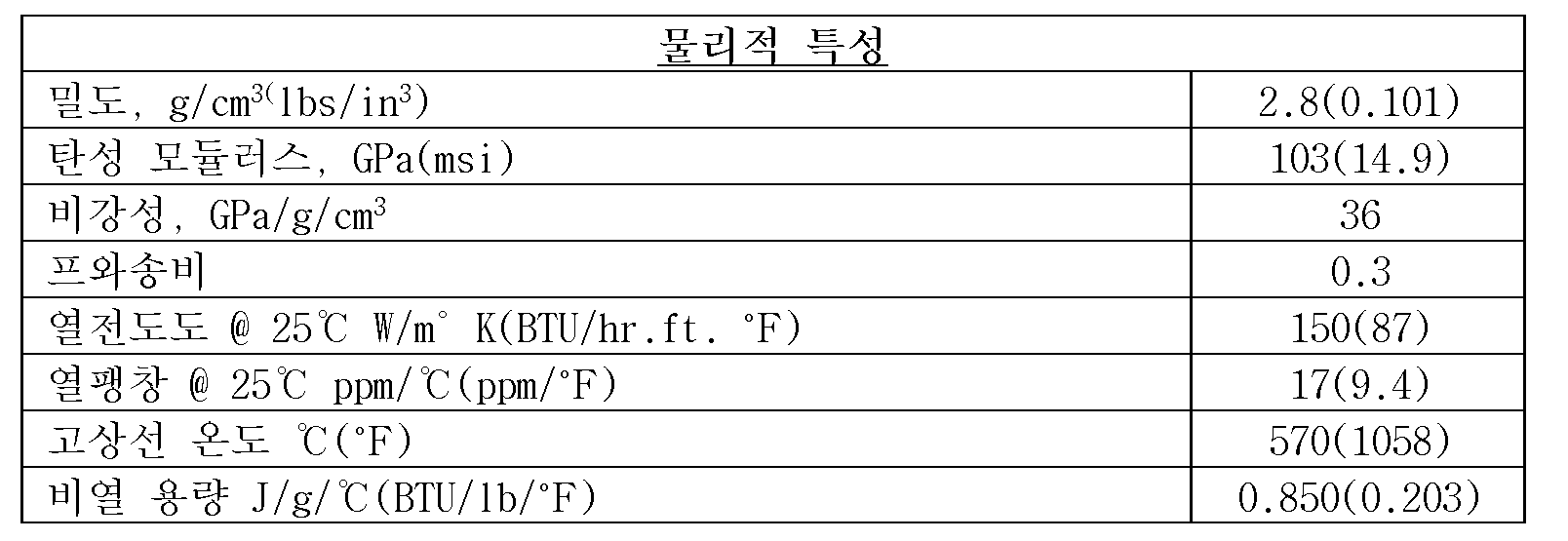
보다 특정한 실시형태에서, MMC는 40 부피%의 탄화규소 입자로 강화된 6061 알루미늄 합금으로 제조될 수 있다. 40 부피%의 탄화규소 입자로 강화된 6061 알루미늄 합금은 상품명 SupremEX 640으로 마테리온(Materion)에서 시판하고 있다. 40 부피%의 탄화규소 입자로 강화된 6061 알루미늄 합금의 물리적 특성은 다음과 같다:In a more specific embodiment, the MMC can be manufactured from a 6061 aluminum alloy reinforced with 40 vol% silicon carbide particles. The 6061 aluminum alloy reinforced with 40 vol% silicon carbide particles is commercially available from Materion under the trade name SupremEX 640. The physical properties of the 6061 aluminum alloy reinforced with 40 vol% silicon carbide particles are as follows:

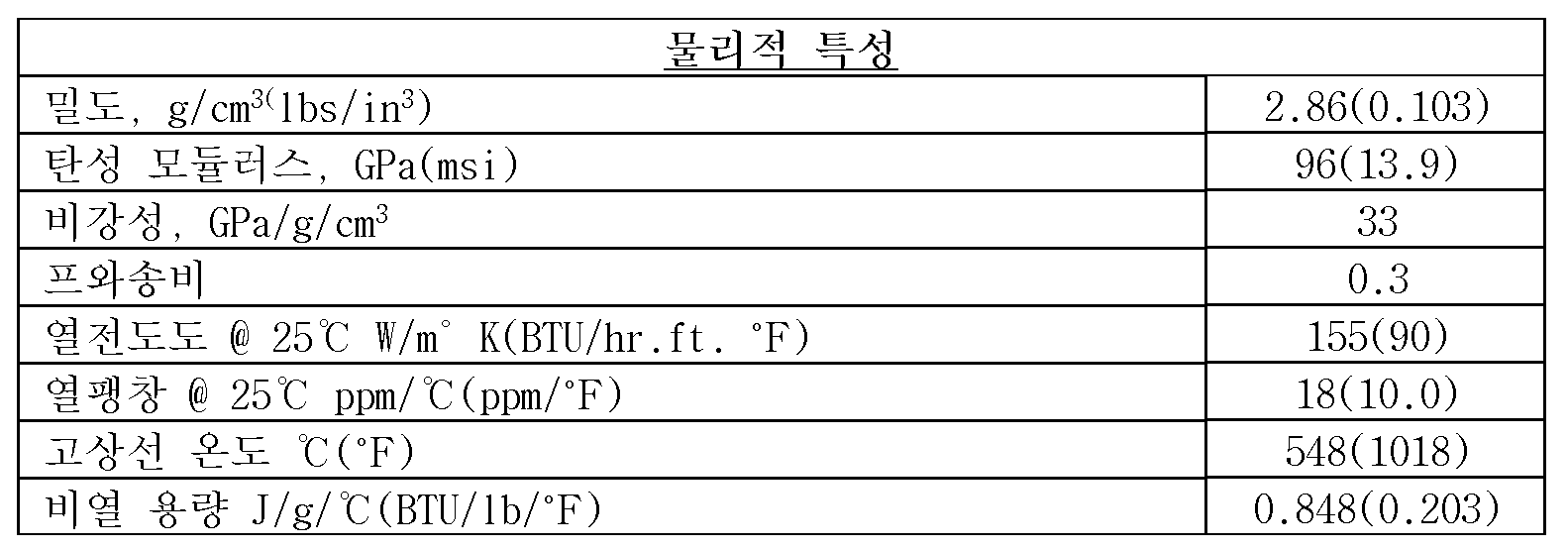
다른 특정한 실시형태에서, MMC는 20 부피%의 탄화규소 입자로 강화된 6061 알루미늄 합금으로 제조될 수 있다. 20 부피%의 탄화규소 입자로 강화된 6061 알루미늄 합금의 물리적 특성은 다음과 같다:In another specific embodiment, the MMC can be manufactured from a 6061 aluminum alloy reinforced with 20 vol.% silicon carbide particles. The physical properties of the 6061 aluminum alloy reinforced with 20 vol.% silicon carbide particles are as follows:
추가의 특정한 실시형태에서, MMC는 25 부피%의 탄화규소 입자로 강화된 2124 알루미늄 합금으로 제조될 수 있다. 25 부피%의 탄화규소 입자로 강화된 2124 알루미늄 합금은 상품명 SupremEX 225로 마테리온에서 시판하고 있다. 25 부피%의 탄화규소 입자로 강화된 2124 알루미늄 합금의 물리적 특성은 다음과 같다:In a further specific embodiment, the MMC can be manufactured from a 2124 aluminum alloy reinforced with 25 vol.% silicon carbide particles. The 2124 aluminum alloy reinforced with 25 vol.% silicon carbide particles is commercially available from Materion under the tradename SupremEX 225. The physical properties of the 2124 aluminum alloy reinforced with 25 vol.% silicon carbide particles are as follows:

특정 실시형태에서, MMC는 17 부피%의 탄화규소 입자로 강화된 2124 알루미늄 합금으로 제조될 수 있다. 17 부피%의 탄화규소 입자로 강화된 2124 알루미늄 합금은 상품명 SupremEX 217XG로 마테리온에서 시판하고 있다. 17 부피%의 탄화규소 입자로 강화된 2124 알루미늄 합금의 물리적 특성은 다음과 같다:In certain embodiments, the MMC can be manufactured from 2124 aluminum alloy reinforced with 17 vol.% silicon carbide particles. 2124 aluminum alloy reinforced with 17 vol.% silicon carbide particles is commercially available from Materion under the trade name SupremEX 217XG. The physical properties of 2124 aluminum alloy reinforced with 17 vol.% silicon carbide particles are as follows:

다른 실시형태에서, MMC는 약 10 부피% 내지 약 wt 부피%의 탄화규소 입자, 예를 들어 약 15 부피% 내지 약 30 부피%, 또는 약 20 부피% 내지 약 25 부피%의 탄화규소 입자로 강화된 6063, 6082, 2009, 또는 2618 계열 알루미늄 합금으로 제조될 수 있다.In another embodiment, the MMC can be manufactured from a 6063, 6082, 2009, or 2618 series aluminum alloy reinforced with about 10 vol % to about wt vol % silicon carbide particles, for example, about 15 vol % to about 30 vol %, or about 20 vol % to about 25 vol % silicon carbide particles.
일부 특정 실시형태에서, MMC는 15 부피%의 탄화규소 입자로 강화된 2009 계열 알루미늄 합금으로 제조된다. 15 부피%의 탄화규소 입자로 강화된 2009 계열 알루미늄 합금의 물리적 특성은 다음과 같다:In some specific embodiments, the MMC is manufactured from a 2009 series aluminum alloy reinforced with 15 vol.% silicon carbide particles. The physical properties of the 2009 series aluminum alloy reinforced with 15 vol.% silicon carbide particles are as follows:
또 다른 실시형태에서, 미러 기판은 카보런덤으로도 알려진 100% 탄화규소(입자 형태가 아님)로 제조될 수 있다. 이러한 기판은 SiC 입자들을 함께 소결하거나, 또는 당 업계에 공지된 다른 수단에 의해 제조될 수 있다.In another embodiment, the mirror substrate can be made of 100% silicon carbide (not in particle form), also known as carborundum. Such substrates can be made by sintering SiC particles together, or by other means known in the art.
또 다른 실시형태에서, 미러 기판은 알루미늄-베릴륨 조성물로 제조된다. 알루미늄-베릴륨 조성물은 베릴륨의 고 모듈러스 및 저밀도 특성을 알루미늄의 제조 및 기계적 특성 거동과 함께 겸비한다. 알루미늄-베릴륨 조성물은 우수한 비강성 및 가공 특성을 제공한다. 알루미늄-베릴륨 금속 매트릭스 복합체는 기계가공 손상(machining damage)에 민감하지 않으며 베릴륨과 같은 기계가공 후 에칭을 필요로 하지 않는다. 베릴륨은 알루미늄과 합금되어 금속 매트릭스 복합체를 형성하였을 때 통상적인 구조 재료에 비해 높은 비탄성 모듈러스, 낮은 밀도 및 높은 열용량의 조합을 생성한다.In another embodiment, the mirror substrate is manufactured from an aluminum-beryllium composition. The aluminum-beryllium composition combines the high modulus and low density properties of beryllium with the manufacturing and mechanical property behavior of aluminum. The aluminum-beryllium composition provides excellent specific stiffness and machining properties. The aluminum-beryllium metal matrix composite is insensitive to machining damage and does not require post-machining etching like beryllium. Beryllium, when alloyed with aluminum to form a metal matrix composite, produces a combination of high specific modulus, low density, and high heat capacity compared to conventional structural materials.
알루미늄-베릴륨 조성물은 약 50 중량% 내지 99.99 중량%의 베릴륨 및 0.01 내지 약 50 중량%의 알루미늄을 함유할 수 있다. 일부 실시형태에서, 알루미늄-베릴륨 조성물은 적어도 60 중량%의 베릴륨 및 적어도 30 중량%의 알루미늄을 함유한다. 베릴륨과 알루미늄의 비율은 알루미늄-베릴륨 조성물의 물리적, 열적 및 기계적 특성을 변화시키기 위해 변경될 수 있다. 생성되는 합금은 금속의 특성을 유지하는 알루미늄 및 베릴륨의 혼합물이며, 현재의 경우(알루미늄과 베릴륨 사이의 융점에서의 큰 차이로 인하여) 금속 상의 혼합물을 포함한다.The aluminum-beryllium composition can contain from about 50 wt % to 99.99 wt % beryllium and from 0.01 wt % to about 50 wt % aluminum. In some embodiments, the aluminum-beryllium composition contains at least 60 wt % beryllium and at least 30 wt % aluminum. The proportions of beryllium and aluminum can be varied to change the physical, thermal and mechanical properties of the aluminum-beryllium composition. The resulting alloy is a mixture of aluminum and beryllium that retains the properties of the metals, and in the present case (due to the large difference in melting points between aluminum and beryllium) comprises a mixture of the metals.
알루미늄-베릴륨 조성물의 일례는 약 62 중량%의 베릴륨 및 약 38 중량%의 알루미늄으로 제조되며, 이는 금속 매트릭스 복합체의 형태이다. 이러한 조성물은 상표명 AlBeMet® 162로 마테리온에서 시판하고 있다. AlBeMet® 162의 물리적 특성은 다음과 같다:An example of an aluminum-beryllium composition is made of about 62 wt% beryllium and about 38 wt% aluminum, in the form of a metal matrix composite. This composition is commercially available from Materion under the trade name AlBeMet® 162. The physical properties of AlBeMet® 162 are as follows:

도 2는 미러 기판의 배면을 나타내는 도면이다. 이와 관련하여, 미러 기판은전형적으로는 전체적으로 목적하는 형상의 미러를 갖는 고체 블랭크로서 형성된다. 다시 도 1을 참조하면, 블랭크는 두 표면 사이에 두께(133)를 갖는 전면(130) 및 배면(131)을 갖는다. 블랭크는 도 2에 도시되어 있는 바와 같이 매끄러운 전면 및 전면을 지지하는 리브(137)를 갖는 개방형 후면 미러를 형성하기 위해 다양한 절삭 공구로 기계가공될 수 있다.FIG. 2 is a drawing showing the back surface of the mirror substrate. In this regard, the mirror substrate is typically formed as a solid blank having a mirror of a desired overall shape. Referring again to FIG. 1, the blank has a front surface (130) and a back surface (131) having a thickness (133) between the two surfaces. The blank can be machined with various cutting tools to form an open back mirror having a smooth front surface and ribs (137) supporting the front surface, as shown in FIG. 2.
미러 기판 블랭크는 상기에서 논의된 분말의 열간 등압 성형("HIP")에 의해 생성될 수 있고, 이어서 미러 기판의 목적하는 형상을 얻기 위해 기계가공될 수 있다. HIP에서, 금속 분말을 적당하거나 목적하는 형상의 금속 캔 또는 용기에 쏟아 붓는다. 용기를 약 670℃ 초과의 온도에서 탈가스화(outgassing)함으로써 배기한 후, 탈가스 튜브를 밀봉한다. 이어서, 용기를 HIP 오토클레이브 장치에 넣고, 이를 가스(예를 들어, 아르곤)로 약 15 ksi 정도로 높게 가압한 다음, 약 1250℃ 이하의 온도로 가열한다. 밀봉된 진공-탈가스화된 용기에서 분말을 통합하는 HIP 프레스의 기능으로 인하여 미러 블랭크는 거의 100% 밀도로 형성될 수 있다. 이어서, 용기를 HIP 오토클레이브에서 회수하고, 추가의 어닐링 단계를 수행할 수 있다. 생성되는 블랭크는 용기와 동일한 형상을 갖는다.Mirror substrate blanks can be produced by hot isostatic pressing (“HIP”) of the powders discussed above, and then machined to obtain the desired shape of the mirror substrate. In HIP, metal powder is poured into a metal can or vessel of a suitable or desired shape. The vessel is evacuated by outgassing at a temperature in excess of about 670° C., and the outgassing tube is sealed. The vessel is then placed in a HIP autoclave, pressurized with a gas (e.g., argon) to as high as about 15 ksi, and then heated to a temperature of up to about 1250° C. Due to the ability of the HIP press to consolidate the powder in the sealed, vacuum-outgassed vessel, the mirror blank can be formed to nearly 100% density. The vessel is then removed from the HIP autoclave and a further annealing step can be performed. The resulting blank has the same shape as the vessel.
HIP 공정은 유리하게는 보이드(void)가 없는 고체 블랭크를 생성한다. 또한, HIP는 모든 방향으로 압력을 가하기 때문에, 최종 생성물의 무 방향성(non-directionality)은 일축 진공 열간 가압 성형(uniaxial vacuum hot pressing)보다 더 잘 유지된다. HIP는 일반적으로는 비교적 단순한 형태를 갖는 미러 기판 블랭크를 생성하는데 사용될 수 있다.The HIP process advantageously produces a solid blank that is void-free. In addition, since HIP applies pressure in all directions, the non-directionality of the final product is better maintained than with uniaxial vacuum hot pressing. HIP can generally be used to produce mirror substrate blanks having relatively simple geometries.
미러 기판 블랭크는 냉간 등압 성형(Cold Isostatic Pressing)에 의해서도 생성할 수 있다. 일부 실시형태에서, 재료는 미세 구조를 갖는 구형 분말을 생성하는 가스 분무 공정에 의해 생성된다. 세 가지 통합 공정은 분말을 고밀도화하여 각각 상이한 기계적 특성을 생성한다. 일부 실시형태에서, 압출봉은 등방성 구형 알루미늄-베릴륨을 반-조밀화된 빌렛으로 냉간 등압 성형(CIP)한 다음 후속 압출을 위해 빌렛을 캐닝(canning)함으로써 제조된다.The mirror substrate blanks can also be produced by Cold Isostatic Pressing. In some embodiments, the material is produced by a gas atomizing process that produces spherical powders having a microstructure. The three integrated processes densify the powders, each producing different mechanical properties. In some embodiments, the extruded rods are produced by Cold Isostatic Pressing (CIP) of isotropic spherical aluminum-beryllium into semi-densified billets, followed by canning the billets for subsequent extrusion.
미러 기판 블랭크는 또한 정밀 정형(NNS: near-net-shaping) 공정에 이어 NNS 블랭크를 기계가공하여 생성할 수도 있다. NNS 공정은 열간 및 냉간 등압 성형(HIP 및 CIP) 및 진공 소결 방법의 조합을 포함할 수 있다. CIP 공정에서, 정밀 정형 블랭크는 목적하는 블랭크 형상을 생성하도록 성형된 가요성 중합체 백(bag)을 사용하여 금속 분말로부터 제조된다. CIP 공정은 더 복잡한 기하학적 구조를 가진 부품에 유용하다. CIP 공정은 진공 소결에 이어, 100%에 근접한 밀도가 요구되는 경우, HIP를 수행한다. 소결은 표면에 연결된 공극을 밀봉하기 때문에, HIP 공정에는 용기가 전혀 필요하지 않다. 경우에 따라, 블랭크를 목적하는 최종 형상으로 열 성형할 수 있다.Mirror substrate blanks can also be produced by machining an NNS blank following a near-net-shaping (NNS) process. The NNS process can include a combination of hot and cold isostatic pressing (HIP and CIP) and vacuum sintering methods. In the CIP process, a near-net-shaping blank is manufactured from metal powder using a flexible polymer bag that is shaped to produce the desired blank shape. The CIP process is useful for parts with more complex geometries. The CIP process is followed by vacuum sintering, followed by HIP when a density close to 100% is required. Since sintering seals the pores connected to the surfaces, no container is required for the HIP process. In some cases, the blank can be thermoformed into the desired final shape.
HIP 또는 NNS에 의해 생성되는 미러 기판 블랭크를 최종 자외선 반사 미러(124)로 변환하는 단계는 일반적으로는 미러 기판(128)을 기계가공하는 단계, 상기 미러 기판의 전면(130)을 연마하는 단계, 및 상기 전면을 자외선 반사 재료(135)로 코팅하는 단계의 세 가지 기본 단계를 수반한다.The process of converting a mirror substrate blank produced by HIP or NNS into a final UV reflective mirror (124) typically involves three basic steps: machining the mirror substrate (128), polishing the front surface (130) of the mirror substrate, and coating the front surface with a UV reflective material (135).
절삭 공구 재료를 사용하는 임의의 기계가공 작업은 공작물(즉, 미러 기판(128))에 응력을 가하지 않고서 수행되어야 한다. 따라서, 일부 실시형태에서, 높은 수준의 기계가공 정밀도를 달성하기 위해 공작 기계에서 가스 베어링을 사용하는 저 응력 기계가공 기술을 사용한다. 이러한 저 응력 기계가공 기술을 사용하면, 미러 기판 표면(130)은 약 15 옹스트롬(Å)(평균 제곱근(rms: root-mean-square)) 정도로 낮은 표면 거칠기로 마감될 수 있다.Any machining operation using cutting tool material should be performed without applying stress to the workpiece (i.e., the mirror substrate (128)). Therefore, in some embodiments, a low-stress machining technique using gas bearings in the machine tool is used to achieve a high level of machining precision. Using such a low-stress machining technique, the mirror substrate surface (130) can be finished with a surface roughness as low as about 15 angstroms (Å) (root-mean-square (rms)).
이어서, 자외선 반사층(135)이 미러 기판(128)의 전면(130) 상에 적용되거나 형성된다. 일부 실시형태에서, 니켈 또는 니켈 합금과 같은 금속으로 제조된 베이스 재료가 베어 미러 기판 상에 증착된다. 이러한 베이스 층의 상부에, 자외선 반사 재료의 하나의 층 또는 다수의 층이 증착된다. 이러한 반사 코팅은 산화하프늄(HfO2) 및 이산화규소의 조합으로부터 형성되는 층과 같은 유전체일 수 있다. 대안적인 반사 코팅은(i) 알루미늄 금속 결합제 및 산화하프늄 및(ii) 알루미늄 금속 결합제 및 이산화규소의 교대 층(alternating layer)이 미러 기판에 적용되는 "강화-알루미늄" 유형일 수 있다.Next, an ultraviolet reflective layer (135) is applied or formed on the front surface (130) of the mirror substrate (128). In some embodiments, a base material made of a metal, such as nickel or a nickel alloy, is deposited on the bare mirror substrate. On top of this base layer, one or more layers of an ultraviolet reflective material are deposited. This reflective coating may be a dielectric, such as a layer formed from a combination of hafnium oxide (HfO 2 ) and silicon dioxide. An alternative reflective coating may be a "reinforced-aluminum" type, in which alternating layers of (i) an aluminum metal binder and hafnium oxide and (ii) an aluminum metal binder and silicon dioxide are applied to the mirror substrate.
이제 도 3을 참조하면, 레이저 어닐링 장치(100)가 도시되어 있다. 이러한 장치(100)는 광학 시스템(120)을 통과하는 원시 레이저 빔(LB)을 생성하는 레이저 빔 발생기(110)를 포함한다. 레이저 빔(LB)은 일반적으로는 엑시머 레이저로서, 이는 10 나노미터 내지 400 나노미터(nm)의 파장에서 자외선을 방출할 수 있는 레이저의 한 가지 형태이다. 엑시머 레이저는 전형적으로는 희가스(아르곤, 크립톤 또는 크세논) 및 반응성 가스(불소 또는 염소)의 조합을 사용한다. 전기 자극 및 고압의 적절한 조건 하에, 자외선 범위의 레이저 광이 생성된다.Referring now to FIG. 3, a laser annealing device (100) is illustrated. The device (100) includes a laser beam generator (110) that generates a raw laser beam (LB) that passes through an optical system (120). The laser beam (LB) is typically an excimer laser, which is a type of laser that can emit ultraviolet light at wavelengths from 10 nanometers to 400 nanometers (nm). Excimer lasers typically use a combination of a noble gas (argon, krypton, or xenon) and a reactive gas (fluorine or chlorine). Under appropriate conditions of electrical stimulation and high pressure, laser light in the ultraviolet range is generated.
광학 시스템(120)은 빔 균질화기 또는 빔 익스팬더(122), 반사 미러(124) 및 초점 렌즈(126)와 같은 다른 광학 구성 요소를 포함할 수 있다. 빔 스플리터가 또한 사용될 수도 있다. 장치 내의 부품의 작동 및 배열에 따라, 이러한 구성 요소들 중 하나 이상이 존재할 수 있다. 이러한 광학 구성 요소는 레이저 빔(LB)을 복수의 선형 레이저 빔으로 분할하고, 이후에 이러한 레이저 빔은 균질화되고 중첩(수렴)되어 최종적으로는 목적하는 빔 폭과 빔 길이를 갖는 단일의 선형 레이저 빔을 형성하는데 사용될 수 있다. 광학 시스템(120)은 단지 설명의 편의를 위해 이러한 방식으로 기능적으로 분할된 것으로만 도시되어 있다. 광학 시스템(120)은 일반적으로는 레이저 빔(LB)의 에너지 분포를 균질화하거나 확장할 수있는 임의의 광학 요소를 포함할 수 있다.The optical system (120) may include other optical components such as a beam homogenizer or beam expander (122), a reflective mirror (124), and a focusing lens (126). A beam splitter may also be used. Depending on the operation and arrangement of the components within the device, one or more of these components may be present. These optical components may be used to split the laser beam (LB) into a plurality of linear laser beams, which are then homogenized and superimposed (converged) to ultimately form a single linear laser beam having a desired beam width and beam length. The optical system (120) is only shown as being functionally split in this manner for convenience of illustration. The optical system (120) may generally include any optical element capable of homogenizing or expanding the energy distribution of the laser beam (LB).
광학 시스템(120)의 미러(124)는 레이저 빔 생성 유닛(110)에서 생성되는 레이저 빔의 경로를 레이저 빔(LB)의 본래의 경로와 다른 방향으로 변경한다. 도 3에 도시되어 있는 바와 같이, 미러(124)는 레이저 빔(LB)의 경로를 본래의 레이저 빔 경로에 수직인 방향으로 변경한다. 다시 말해, 미러(124)는 레이저 빔을 초점 렌즈(126) 상에 투사하기 위해 레이저 빔을 반사하거나 또는 조향함으로써, 레이저 빔은 전자 디스플레이의 생산에 사용되는 기판(140)의 노출된 표면을 조사하게 된다. 미러(124)는 레이저 빔 발생기(110)에 대해 미러의 위치를 변경할 수 있는 모터(도시되지 않음) 및 구동 시스템에 연결될 수 있다.The mirror (124) of the optical system (120) changes the path of the laser beam generated from the laser beam generating unit (110) to a direction different from the original path of the laser beam (LB). As illustrated in FIG. 3, the mirror (124) changes the path of the laser beam (LB) to a direction perpendicular to the original laser beam path. In other words, the mirror (124) reflects or steers the laser beam to project the laser beam onto the focusing lens (126), so that the laser beam irradiates the exposed surface of the substrate (140) used in the production of the electronic display. The mirror (124) may be connected to a motor (not illustrated) and a drive system that can change the position of the mirror with respect to the laser beam generator (110).
초점 렌즈(126)는 분할된 선형 레이저 빔을 집중시켜 단일의 선형 레이저 빔을 형성한다. 바람직하게는, 분할된 선형 레이저 빔은 기판(140)의 노출된 상부 표면 상에 집중된다. 즉, 분할된 선형 레이저 빔은 서로 중첩되어 단일의 선형 레이저 빔을 형성한다. 원통형 렌즈가 초점 렌즈(126)로서 사용될 수 있다. 광학 시스템(120)으로부터 출력된 단일의 선형 레이저 빔이 기판(140) 상에 투사된 후, 선형 레이저 빔은 고정된 스캔 피치를 따라 선형 레이저 빔의 길이 방향에 수직인 방향으로 이동함으로써 기판(140)의 노출된 상부 표면을 스캔한다. 대안적으로, 기판(140)을 고정하기 위한 스테이지(150)가 선형 레이저 빔이 이동하는 방향과 반대 방향으로 이동할 수 있다. 일부 실시형태에서, 기판(140)의 노출된 표면 상에 출력 레이저 빔을 조사한 결과, 비정질 실리콘 박막 필름이 어닐링되어 폴리실리콘 필름을 생성한다. 다시 말해, 엑시머 레이저 어닐링("ELA")에 의해 폴리실리콘 필름이 형성된다. 보다 일반적으로는, 비정질 필름은 엑시머 레이저 어닐링을 통해 전구체 필름으로부터 형성될 수 있다.The focusing lens (126) focuses the split linear laser beam to form a single linear laser beam. Preferably, the split linear laser beam is focused on the exposed upper surface of the substrate (140). That is, the split linear laser beams overlap each other to form a single linear laser beam. A cylindrical lens may be used as the focusing lens (126). After the single linear laser beam output from the optical system (120) is projected onto the substrate (140), the linear laser beam scans the exposed upper surface of the substrate (140) by moving in a direction perpendicular to the longitudinal direction of the linear laser beam along a fixed scan pitch. Alternatively, the stage (150) for fixing the substrate (140) may move in a direction opposite to the direction in which the linear laser beam moves. In some embodiments, as a result of irradiating the output laser beam on the exposed surface of the substrate (140), the amorphous silicon thin film is annealed to produce a polysilicon film. In other words, a polysilicon film is formed by excimer laser annealing (“ELA”). More generally, an amorphous film can be formed from a precursor film by excimer laser annealing.
도 4는 유기 발광 다이오드 디스플레이와 같은 전자 디스플레이의 제조시에 사용되는 폴리실리콘 필름을 형성하기 위한 공정의 사시도를 도시한다. 폴리실리콘 필름은 상술된 도 3의 실시형태에 따라 엑시머 레이저 빔을 스캔하고 조사하는 ELA 장치로 형성된다. 도 4에 도시되어 있는 바와 같이, 전자 디스플레이는 기판 본체(140), 기판 본체(140) 상에 형성된 버퍼층(142), 및 버퍼층(142) 상에 형성된 얇은 비정질 필름(144)을 포함한다. 기판 본체(140)는 유리, 석영, 세라믹, 플라스틱 등으로 이루어진 절연성 기판으로 또는 플라스틱으로 제조된 가요성 기판으로 형성된다. 버퍼층(142)은 불순물 원자 또는 수분과 같은 불필요한 원소의 침투를 방지하고 표면을 평탄화한다. 그러나, 버퍼층(142)이 반드시 필요한 것은 아니며 생략될 수도 있다. 비정질 필름(144)은 일반적으로는 박막 트랜지스터(도시되지 않음)의 일부로서 포함되는 반도체 층(도시되지 않음)을 제조하는데 사용된다. 비정질 필름(144)은 레이저 빔(LB)을 전구체 필름(도시되지 않음) 상에 주사하고 조사함으로써 형성된다. 실리콘 필름을 생성하기 위해, 비정질 실리콘 필름은 미세 결정질 실리콘 필름을 형성하기 위해 레이저 조사 이전에 열처리될 수 있다.FIG. 4 is a perspective view of a process for forming a polysilicon film used in the manufacture of an electronic display such as an organic light emitting diode display. The polysilicon film is formed by an ELA device that scans and irradiates an excimer laser beam according to the embodiment of FIG. 3 described above. As shown in FIG. 4, the electronic display includes a substrate body (140), a buffer layer (142) formed on the substrate body (140), and a thin amorphous film (144) formed on the buffer layer (142). The substrate body (140) is formed of an insulating substrate made of glass, quartz, ceramic, plastic, or the like, or a flexible substrate made of plastic. The buffer layer (142) prevents the penetration of unnecessary elements such as impurity atoms or moisture and flattens the surface. However, the buffer layer (142) is not necessarily required and may be omitted. The amorphous film (144) is generally used to manufacture a semiconductor layer (not shown) included as a part of a thin film transistor (not shown). An amorphous film (144) is formed by scanning and irradiating a laser beam (LB) onto a precursor film (not shown). To produce a silicon film, the amorphous silicon film may be heat treated prior to laser irradiation to form a microcrystalline silicon film.
여기에서 예시되는 바와 같이, 비교적 넓은 영역을 다결정화하기 위해, 레이저 빔(LB)이 비정질 실리콘 필름 상에 2회 이상 주사되고 조사될 수 있다. 레이저 빔(LB)은 공정 공차로 인해 폭 방향으로 부분적으로 중첩되도록 주사되고 조사될 수 있다. 여기에서 예시되는 바와 같이, 레이저 빔(LB)은 화살표 방향으로 이동하여 2개의 단일 조사 영역(SS) 및 레이저 스캐닝의 중첩을 나타내는 이중 조사 영역(DS)을 형성한다. 폴리실리콘 필름(144)은 레이저 빔(LB)으로 1회 조사되는 단일 조사 영역(SS) 및 레이저 빔(LB)으로 2회 조사되는 이중 조사 영역(DS)으로 구분될 수 있다.As exemplified herein, in order to polycrystallize a relatively wide area, the laser beam (LB) may be scanned and irradiated twice or more on the amorphous silicon film. The laser beam (LB) may be scanned and irradiated so as to partially overlap in the width direction due to process tolerance. As exemplified herein, the laser beam (LB) moves in the direction of the arrow to form two single irradiation areas (SS) and a dual irradiation area (DS) representing the overlap of laser scanning. The polysilicon film (144) may be divided into a single irradiation area (SS) irradiated once with the laser beam (LB) and a dual irradiation area (DS) irradiated twice with the laser beam (LB).
또한, 이중 조사 영역(DS)이 단일 조사 영역(SS)의 레이저 에너지와 다른 레이저 에너지를 수신하거나, 또는 선형 레이저 빔의 목적하는 에너지 분포 프로파일이 변화하는 경우(예를 들어, 기판 또는 비정질 실리콘 필름의 두께가 어닐링 동안 변화하는 경우), 선형 레이저 빔의 형상을 조정하고 에너지 분포 프로파일을 조정하는 조정 장치가 도 3의 장치(100)에 포함될 수도 있다. 특히, 장치(100)는 기판(140)에 대한 초점 렌즈(126)의 수직 거리(즉, 미러(124)에 더 가까워지거나 더 멀어짐) 및 회전 각도를 변경할 수 있는 초점 렌즈 조정 장치(도시되지 않음)를 포함할 수 있다. 따라서, 비록 레이저 빔의 목적하는 에너지 분포 프로파일은 변경될 수 있지만, 레이저 빔의 목적하는 에너지 분포 프로파일은 광학 시스템(120)을 리셋하지 않고서도 초점 렌즈 조정 장치를 사용함으로써 여전히 획득할 수 있다.Additionally, if the dual irradiation region (DS) receives different laser energy than the single irradiation region (SS), or if the desired energy distribution profile of the linear laser beam changes (e.g., if the thickness of the substrate or the amorphous silicon film changes during annealing), an adjustment device for adjusting the shape of the linear laser beam and adjusting the energy distribution profile may be included in the device (100) of FIG. 3. In particular, the device (100) may include a focus lens adjustment device (not shown) that can change the vertical distance (i.e., closer to or farther from the mirror (124)) and rotation angle of the focus lens (126) with respect to the substrate (140). Thus, although the desired energy distribution profile of the laser beam may change, the desired energy distribution profile of the laser beam can still be obtained by using the focus lens adjustment device without resetting the optical system (120).
본 발명의 반사 미러는, 예를 들면, 레이저 리프트 오프("LLO") 공정과 같은 레이저의 사용을 필요로 하는 다른 전자 디스플레이 형성 공정에서 사용될 수 있다. LLO에서, 전구체 필름은 임시 기판 상에 증착되며, 다른 처리 작업 및 구조는 박막 필름의 대향 표면 상에서 발생한다. 이어서, 레이저 빔은 임시 기판을 통해 전달되어 기판-필름 계면을 조사한다. 이는 임시 기판으로부터 전구체 필름의 제거를 가능하게 하며(즉, 필름이 기판에서 "리프트 오프"됨), 전구체 박막 필름은 목적하는 특성을 갖는 영구 기판으로 전사될 수 있다. 본 발명의 반사 미러는 또한 ELA 또는 LLO 이외의 다른 시스템, 예를 들어 UV 리소그래피, 안과 수술, 및 치과 수술 시스템에서 사용될 수도 있다.The reflective mirrors of the present invention may be used in other electronic display formation processes that require the use of a laser, such as, for example, a laser lift-off ("LLO") process. In LLO, a precursor film is deposited on a temporary substrate, and other processing operations and structures occur on the opposing surface of the thin film. A laser beam is then transmitted through the temporary substrate to irradiate the substrate-film interface. This allows removal of the precursor film from the temporary substrate (i.e., the film is "lifted off" of the substrate), so that the precursor thin film can be transferred to a permanent substrate having the desired properties. The reflective mirrors of the present invention may also be used in systems other than ELA or LLO, such as UV lithography, ophthalmic surgical, and dental surgical systems.
도 5를 참조하면, LLO 처리에 적합한 적층체가 예시되어 있다. 도 5의 적층체는 임시 기판(240) 상에 형성된 박막 필름(244)을 포함한다. 박막 필름(244)과 임시 기판(240) 사이의 계면은 도면 부호(242)로 표시된다. 계면(242)은 단순히 박막 필름(244)의 일부일 수 있거나, 또는 엑시머 레이저에 의해 분해될 수 있는 희생 물질로부터 형성되는 층일 수 있다.Referring to FIG. 5, a laminate suitable for LLO processing is illustrated. The laminate of FIG. 5 includes a thin film (244) formed on a temporary substrate (240). An interface between the thin film (244) and the temporary substrate (240) is indicated by reference numeral (242). The interface (242) may simply be a portion of the thin film (244), or may be a layer formed from a sacrificial material that can be decomposed by an excimer laser.
임시 기판(240)은 목적하는 박막 필름(244)을 형성하는 고온 필름 형성 공정에서 내구성이 있는 재료로 형성된다. 임시 기판(240)은 레이저 빔의 파장에 상응하는 밴드 갭 에너지보다 더 큰 밴드 갭 에너지를 갖는 재료로 형성되며, 따라서 레이저 빔은 임시 기판(240)을 투과할 수 있다. 임시 기판(240)은 투명 기판일 수 있다. 임시 기판(240)은 사파이어, 석영, 유리, 산화마그네슘(MgO), 란타늄 알루미네이트(LaAlO3), 용융 실리카, 또는 지르코니아 중 어느 하나로 형성될 수 있다.The temporary substrate (240) is formed of a durable material in a high temperature film forming process for forming a desired thin film (244). The temporary substrate (240) is formed of a material having a band gap energy greater than a band gap energy corresponding to a wavelength of a laser beam, so that the laser beam can transmit through the temporary substrate (240). The temporary substrate (240) may be a transparent substrate. The temporary substrate (240) may be formed of any one of sapphire, quartz, glass, magnesium oxide (MgO), lanthanum aluminate (LaAlO 3 ), fused silica, or zirconia.
박막 필름(244)을 제거하기 위해, 도 3에 도시되고 상술된 (빔 균질화기 또는 익스팬더(122), 베릴륨 미러(124), 및 초점 렌즈(126)를 포함하는) 광학 시스템(120)을 사용하여 계면(242) 상에 레이저 에너지를 집중시킬 수 있다.To remove the thin film (244), the laser energy can be focused onto the interface (242) using an optical system (120) (including a beam homogenizer or expander (122), a beryllium mirror (124), and a focusing lens (126)) as shown in FIG. 3 and described above.
박막 필름(244)은 목적하는 전자 디스플레이 장치의 기능성 유닛을 형성하는데 사용되는 구조를 갖는다. 박막 필름(244)은 반도체 또는 폴리실리콘과 같은 무기 재료 또는 금속으로 형성될 수 있다. 대안적으로, 박막 필름(244)은 디스플레이 장치용 비정질 실리콘 또는 폴리실리콘으로 형성될 수 있다. 보다 일반적으로, 이러한 박막 필름은 전구체 필름이라 지칭된다.The thin film (244) has a structure used to form a functional unit of the intended electronic display device. The thin film (244) may be formed of an inorganic material such as a semiconductor or polysilicon or a metal. Alternatively, the thin film (244) may be formed of amorphous silicon or polysilicon for the display device. More generally, such a thin film is referred to as a precursor film.
도 6a 및 도 6b는 LLO를 사용하는 디스플레이 장치를 제조하기 위한 전사 공정의 일례를 예시하는 단면도이다. 도 6a에 예시된 제 1 위치에서, 계면(242)은 박막 필름(244)이 임시 기판(240)으로부터 분리되도록 레이저 장치(100)에 의해 표적화된다. 동시에, 박막 필름(244)은 전사 롤(250)의 원주 표면에 밀착되어 일시적으로 결합될 수 있다. 이러한 공정은 전사 롤의 일측(여기서는, 하단부) 상에서 발생한다.FIGS. 6A and 6B are cross-sectional views illustrating an example of a transfer process for manufacturing a display device using LLO. At the first position illustrated in FIG. 6A, an interface (242) is targeted by a laser device (100) so that a thin film (244) is separated from a temporary substrate (240). At the same time, the thin film (244) can be temporarily bonded to and adhered to a circumferential surface of a transfer roll (250). This process occurs on one side (here, the lower end) of the transfer roll.
이와 동시에, 도 6b에 도시되어 있는 바와 같이, 전사 롤의 다른 일측 상에서는, 영구 기판(260)이 구동되어 박막 필름(244)이 전사 롤의 제 2 위치에서 전사 롤(250)로부터 영구 기판(260)의 표면으로 전사된다. 여기서, 영구 기판(260) 및 박막 필름(244)은 디스플레이 장치를 구성한다. 경우에 따라, 영구 기판(260)과 박막 필름(244) 사이의 결합을 강화하기 위해 접착제 층(270)이 영구 기판(260) 위에 추가로 코팅될 수 있다.At the same time, as illustrated in FIG. 6b, on the other side of the transfer roll, the permanent substrate (260) is driven so that the thin film (244) is transferred from the transfer roll (250) to the surface of the permanent substrate (260) at the second position of the transfer roll. Here, the permanent substrate (260) and the thin film (244) constitute a display device. In some cases, an adhesive layer (270) may be additionally coated on the permanent substrate (260) to strengthen the bonding between the permanent substrate (260) and the thin film (244).
이러한 제조 장치의 자외선 반사 미러에서 미러 기판으로 알루미늄 MMC 또는 탄화규소를 사용하면 증가된 생산 수요를 충족시키기 위해 종래의 용융 석영 기반 미러보다 개선된 성능을 제공한다. 예를 들어, 도 7 내지 도 10은 다른 기판 재료 이외에도 MMC 또는 탄화규소로 형성된 기판 및 용융 석영 기반 기판을 포함한 기판에 대한 광학 FoM 값(즉, 서로에 대한 다양한 기판 재료의 성능을 특성화하는데 사용되는 값)을 예시한다. 특히, 도 7 내지 도 10에서, 막대(1)는 소결된 탄화규소를 나타내고; 막대(2)는 상품명 SupremEX® 640XA로 마테리온에서 시판하고 있는 알루미늄 금속 매트릭스 복합 재료를 나타내고; 막대(3)는 알루미늄 및 30 부피%의 탄화규소 금속 매트릭스 복합 재료를 나타내고; 막대(4)는 용융 석영을 나타내고; 막대(5)는 몰리브덴을 나타내고; 막대(6)는 6061 알루미늄 합금을 나타내며; 막대(7)는 텅스텐을 나타낸다.The use of aluminum MMC or silicon carbide as the mirror substrate in the UV reflecting mirrors of these manufacturing devices provides improved performance over conventional fused quartz-based mirrors to meet increased production demands. For example, FIGS. 7-10 illustrate optical FoM values (i.e., values used to characterize the performance of various substrate materials relative to one another) for substrates formed of MMC or silicon carbide and fused quartz-based substrates, in addition to other substrate materials. In particular, in FIGS. 7-10 , rod (1) represents sintered silicon carbide; rod (2) represents an aluminum metal matrix composite material commercially available from Materion under the tradename SupremEX® 640XA; rod (3) represents an aluminum and 30 vol.% silicon carbide metal matrix composite material; rod (4) represents fused quartz; rod (5) represents molybdenum; rod (6) represents 6061 aluminum alloy; and rod (7) represents tungsten.
도 7은 광학 FoM 공진 주파수 값을 예시한다. 도 7에서, 더 높은 FoM 공진 주파수 값이 기판에 대해 바람직하다. 따라서, 도시되어 있는 바와 같이, 기판의 선호도는 일반적으로 좌측에서 우측으로 감소한다. 도 7의 그래프 상의 굵은 수평선은 용융 석영의 FoM 공진 주파수 값(즉, 막대(4))을 나타내는 것으로, 이는 바람직하게는 달성되어야 하는 최소값(즉, 적어도 6의 FoM 값)이다. 도 7에서 볼 수 있는 바와 같이, 몰리브덴, 알루미늄 6061, 및 텅스텐 기판은 이러한 바람직한 FoM 값을 달성하지 못하였다. 이에 비해, 소결된 탄화규소 또는 알루미늄 기반 MMC로부터 형성된 기판은 바람직한 FoM 값을 달성하였다. 다시 말해, 소결된 탄화규소 및 MMC 기판은 융합 석영 기반 기판보다 훨씬 더 우수한 성능을 발휘하였다, 즉 소결된 탄화규소가 다른 모든 기판보다 성능이 뛰어났다.Figure 7 illustrates the optical FoM resonance frequency values. In Figure 7, a higher FoM resonance frequency value is desirable for the substrate. Therefore, as shown, the preference of the substrate generally decreases from left to right. The thick horizontal line on the graph of Figure 7 represents the FoM resonance frequency value of fused quartz (i.e., bar (4)), which is the minimum value that should preferably be achieved (i.e., a FoM value of at least 6). As can be seen in Figure 7, the molybdenum, aluminum 6061, and tungsten substrates did not achieve these desirable FoM values. In comparison, the substrates formed from sintered silicon carbide or aluminum-based MMCs achieved the desirable FoM values. In other words, the sintered silicon carbide and MMC substrates performed significantly better than the fused quartz-based substrates, i.e., the sintered silicon carbide outperformed all other substrates.
도 8은 광학 FoM 자중 편향 값을 예시한다. 도 8에서, 더 낮은 FoM 자중 편향 값이 기판에 대해 바람직하다. 따라서, 도시되어 있는 바와 같이, 기판의 선호도는 다시 일반적으로 좌측에서 우측으로 감소한다. 도 8의 그래프 상의 굵은 수평선은 용융 석영의 FoM 자중 편향 값(즉, 막대(4))을 나타내는 것으로, 이는 바람직하게는 달성되어야 하는 최대값(즉, 0.030 미만의 FoM 값)이다. 도 8에서 볼 수 있는 바와 같이, 몰리브덴, 알루미늄 6061, 및 텅스텐 기판은 이러한 바람직한 FoM 값을 달성하지 못하였다. 이에 비해, 소결된 탄화규소 또는 알루미늄 기반 MMC로부터 형성된 기판은 바람직한 FoM 값을 달성하였다. 다시 말해, 소결된 탄화규소 및 MMC 기판은 다시 융합 석영 기반 기판보다 훨씬 더 우수한 성능을 발휘하였다, 즉 소결된 탄화규소가 다른 모든 기판보다 성능이 뛰어났다.Figure 8 illustrates the optical FoM self-weight deflection values. In Figure 8, a lower FoM self-weight deflection value is desirable for the substrate. Thus, as shown, the substrate preference again generally decreases from left to right. The thick horizontal line on the graph of Figure 8 represents the FoM self-weight deflection value of fused quartz (i.e., bar (4)), which is the maximum value that should preferably be achieved (i.e., a FoM value less than 0.030). As can be seen in Figure 8, the molybdenum, aluminum 6061, and tungsten substrates did not achieve these desirable FoM values. In comparison, the substrates formed from sintered silicon carbide or aluminum-based MMCs achieved the desirable FoM values. In other words, the sintered silicon carbide and MMC substrates again performed significantly better than the fused quartz-based substrate, i.e., the sintered silicon carbide outperformed all other substrates.
도 9는 광학 FoM 정상상태 열 왜곡 계수 값을 예시한다. 도 9에서, 더 낮은 FoM 정상상태 열 왜곡 계수 값이 기판에 대해 바람직하다. 따라서, 도시되어 있는 바와 같이, 기판의 선호도는 다시 일반적으로 좌측에서 우측으로 감소한다. 도 9의 그래프 상의 굵은 수평선은 용융 석영의 FoM 정상상태 열 왜곡 계수 값(즉, 막대(4))을 나타내는 것으로, 이는 바람직하게는 달성되어야 하는 최대값(즉, 0.350 미만의 FoM 값)이다. 도 9에서 볼 수 있는 바와 같이, 다른 모든 기판은 이러한 바람직한 FoM 값을 달성하였다. 다시 말해, 소결된 탄화규소 및 MMC 기판은 다시 융합 석영 기반 기판보다 훨씬 더 우수한 성능을 발휘하였다, 즉 소결된 탄화규소가 다른 모든 기판보다 성능이 뛰어났다.Figure 9 illustrates the optical FoM steady-state thermal distortion coefficient values. In Figure 9, a lower FoM steady-state thermal distortion coefficient value is desirable for a substrate. Thus, as shown, the substrate preference again generally decreases from left to right. The thick horizontal line on the graph of Figure 9 represents the FoM steady-state thermal distortion coefficient value of fused quartz (i.e., bar (4)), which is the maximum value that should preferably be achieved (i.e., a FoM value less than 0.350). As can be seen in Figure 9, all other substrates achieved these desirable FoM values. In other words, the sintered silicon carbide and MMC substrates again performed significantly better than the fused quartz based substrate, i.e., the sintered silicon carbide outperformed all other substrates.
마지막으로, 도 10은 광학 FoM 과도 열 왜곡 계수 값을 예시한다. 도 10에서, 더 낮은 FoM 과도 열 왜곡 계수 값이 기판에 대해 바람직하다. 따라서, 도시되어 있는 바와 같이, 기판의 선호도는 다시 일반적으로 좌측에서 우측으로 감소한다. 도 10의 그래프 상의 굵은 수평선은 용융 석영의 FoM 과도 열 왜곡 계수 값(즉, 막대(4))을 나타내는 것으로, 이는 바람직하게는 달성되어야 하는 최대값(즉, 0.600 미만의 FoM 값)이다. 도 10에서 볼 수 있는 바와 같이, 다른 모든 기판은 이러한 바람직한 FoM 값을 달성하였다. 다시 말해, 소결된 탄화규소 및 MMC 기판은 다시 융합 석영 기반 기판보다 훨씬 더 우수한 성능을 발휘하였다, 즉 소결된 탄화규소가 다른 모든 기판보다 성능이 뛰어났다.Finally, Fig. 10 illustrates the optical FoM transient thermal distortion coefficient values. In Fig. 10, a lower FoM transient thermal distortion coefficient value is desirable for the substrate. Thus, as shown, the substrate preference again generally decreases from left to right. The thick horizontal line on the graph of Fig. 10 represents the FoM transient thermal distortion coefficient value of fused quartz (i.e., bar (4)), which is the maximum value that should preferably be achieved (i.e., a FoM value less than 0.600). As can be seen in Fig. 10, all other substrates achieved these desirable FoM values. In other words, the sintered silicon carbide and MMC substrates again performed significantly better than the fused quartz based substrate, i.e., the sintered silicon carbide outperformed all other substrates.
이와 같이, 본 발명의 기판은 바람직하게는 (i) 용융 석영 기판에 대해 적어도 6의 광학 FoM 공진 주파수 값; (ii) 용융 석영 기판에 대해 0.030 미만의 광학 FoM 자중 편향 값; (iii) 용융 석영 기판에 대해 0.350 미만의 광학 FoM 정상상태 열 왜곡 계수 값; 및 (iv) 용융 석영 기판에 대해 0.600 미만의 광학 FoM 과도 열 왜곡 계수 값을 갖는 재료로 제조된다.As such, the substrate of the present invention is preferably made of a material having (i) an optical FoM resonant frequency value of at least 6 with respect to the fused quartz substrate; (ii) an optical FoM self-weight deflection value of less than 0.030 with respect to the fused quartz substrate; (iii) an optical FoM steady-state thermal distortion coefficient value of less than 0.350 with respect to the fused quartz substrate; and (iv) an optical FoM transient thermal distortion coefficient value of less than 0.600 with respect to the fused quartz substrate.
이러한 제조 장치의 자외선 반사 미러에서 기판에 대해 개시된 베릴륨-함유 재료를 사용하면 증가된 생산 수요를 충족시키기 위해 종래의 석영 기반 미러보다 개선된 성능을 제공한다. 예를 들어, 베릴륨의 더 높은 강성 이외에도 석영보다 더 빠르게 열을 발산하는 베릴륨의 능력은 해상도에 영향을 미치지 않고서도 본 발명의 미러를 사용하는 레이저의 래스터링 속도를 증가시킬 수 있다. 따라서, 처리량을 증가시킬 수 있고, 대형 디스플레이의 생산에 내재된 장기적인 열 응력으로 인해 석영 미러에서 발생할 수 있는 손상없이 대형 디스플레이를 생산할 수 있으며, 생산 장비의 유지 보수를 위한 가동 중단 시간을 줄일 수 있다.The use of the disclosed beryllium-containing materials for the substrate in the UV reflecting mirrors of these manufacturing devices provides improved performance over conventional quartz-based mirrors to meet increased production demands. For example, in addition to the higher stiffness of beryllium, the ability of beryllium to dissipate heat more quickly than quartz allows for increased rastering speeds of lasers using the mirrors of the present invention without affecting resolution. This can result in increased throughput, production of large displays without damage to quartz mirrors that can occur due to long-term thermal stresses inherent in the production of large displays, and reduced downtime for maintenance of production equipment.
상기 개시된 특징 및 기능 및 다른 특징 및 기능의 변형, 또는 이들의 대안은 많은 다른 상이한 시스템 또는 응용 분야에 조합될 수 있음을 이해할 것이다. 현재 예측하지 못하거나 예상치 못한 다양한 대안, 수정, 변경 또는 개선이 또한 이후에 당업자에 의해 하기 청구범위에 포함되도록 의도될 수 있다.It will be appreciated that the features and functions disclosed above, as well as variations of other features and functions, or alternatives thereof, may be combined in many different systems or applications. Various alternatives, modifications, changes or improvements, not yet anticipated or anticipated, may also be intended to be included in the scope of the claims below by those skilled in the art.
Claims (27)
상기 자외선 레이저로부터 생성되는 레이저 빔을 반사하도록 구성된 적어도 하나의 반사 미러(reflective mirror)
를 포함하는 장치로서,
상기 적어도 하나의 미러는 탄화규소 또는 알루미늄 금속 매트릭스 복합체로 제조되는 미러 기판을 포함하고,
상기 미러 기판은 용융 석영 기판에 대해 적어도 6의 광학 성능 지수(FoM: Figure of Merit) 공진 주파수 값을 갖는,
전자 부품의 생산에 사용하기 위한 장치.ultraviolet laser; and
At least one reflective mirror configured to reflect a laser beam generated from the above ultraviolet laser
As a device comprising:
wherein at least one of the mirrors comprises a mirror substrate made of a silicon carbide or aluminum metal matrix composite,
The above mirror substrate has an optical figure of merit (FoM: Figure of Merit) resonant frequency value of at least 6 with respect to the fused quartz substrate.
A device for use in the production of electronic components.
상기 미러 기판은,
용융 석영 기판에 대해 0.030 미만의 광학 FoM 자중 편향(self-weight deflection) 값;
용융 석영 기판에 대해 0.350 미만의 광학 FoM 정상상태 열 왜곡 계수(thermal distortion coefficient) 값; 및
용융 석영 기판에 대해 0.600 미만의 광학 FoM 과도 열 왜곡 계수(transient thermal distortion coefficient) 값
을 추가로 갖는, 전자 부품의 생산에 사용하기 위한 장치.In paragraph 1,
The above mirror substrate is,
Optical FoM self-weight deflection values less than 0.030 for fused quartz substrates;
An optical FoM steady-state thermal distortion coefficient value of less than 0.350 for the fused quartz substrate; and
Optical FoM transient thermal distortion coefficient values less than 0.600 for fused quartz substrates
A device for use in the production of electronic components, having an additional .
상기 미러 기판은, 알루미늄 합금 및 하나 이상의 강화 입자(reinforcing particle)로 이루어진 알루미늄 금속 매트릭스 복합체로 제조되는, 전자 부품의 생산에 사용하기 위한 장치.In paragraph 1,
A device for use in the production of electronic components, wherein the mirror substrate is manufactured from an aluminum metal matrix composite comprising an aluminum alloy and one or more reinforcing particles.
상기 하나 이상의 강화 입자는 탄화물, 산화물, 규화물, 붕화물, 및 질화물로 이루어진 군으로부터 선택되는 적어도 하나의 세라믹 재료를 포함하는, 전자 부품의 생산에 사용하기 위한 장치.In the third paragraph,
A device for use in the production of electronic components, wherein said one or more reinforcing particles comprise at least one ceramic material selected from the group consisting of carbides, oxides, silicides, borides, and nitrides.
상기 하나 이상의 강화 입자는 탄화규소를 포함하는, 전자 부품의 생산에 사용하기 위한 장치.In the third paragraph,
A device for use in the production of electronic components, wherein said one or more reinforcing particles comprise silicon carbide.
상기 금속 매트릭스 복합체는, 15 부피% 내지 40 부피%의 탄화규소로 강화된 6061, 6063, 6082, 2009, 2618 또는 2124 알루미늄 합금을 포함하는, 전자 부품의 생산에 사용하기 위한 장치.In the third paragraph,
A device for use in the production of electronic components, wherein the metal matrix composite comprises a 6061, 6063, 6082, 2009, 2618 or 2124 aluminum alloy reinforced with 15 to 40 vol% silicon carbide.
상기 미러 기판 상에 자외선 반사 코팅이 증착되고(deposited), 상기 자외선 반사 코팅은 이산화하프늄(HfO2) 및 이산화규소(SiO2)의 조합으로부터 제조되는 층이거나, 또는 상기 자외선 반사 코팅은 (i) 알루미늄 및 산화하프늄으로부터 형성되는 코팅과 (ii) 알루미늄 및 이산화규소로부터 형성되는 코팅의 교번되는 층들(alternating layers)로 형성되는, 전자 부품의 생산에 사용하기 위한 장치.In paragraph 1,
An apparatus for use in the production of electronic components, wherein an ultraviolet reflective coating is deposited on the mirror substrate, the ultraviolet reflective coating being a layer made from a combination of hafnium dioxide (HfO 2 ) and silicon dioxide (SiO 2 ), or the ultraviolet reflective coating is formed of alternating layers of (i) a coating formed from aluminum and hafnium oxide and (ii) a coating formed from aluminum and silicon dioxide.
빔 균질화기(beam homogenizer), 빔 익스팬더(beam expander), 초점 렌즈(focusing lens), 또는 빔 스플리터(beam splitter)를 추가로 포함하는, 전자 부품의 생산에 사용하기 위한 장치.In paragraph 1,
An apparatus for use in the production of electronic components, further comprising a beam homogenizer, a beam expander, a focusing lens, or a beam splitter.
자외선 레이저, 및 미러 기판을 포함하는 적어도 하나의 반사 미러를 포함하는 자외선 레이저 장치를 수용하는 단계;
상기 자외선 레이저로 레이저 빔을 생성하는 단계; 및
상기 적어도 하나의 반사 미러를 사용하여 상기 레이저 빔을 전구체 필름을 향해 반사하여 전자 부품을 생성하는 단계
를 포함하며; 이때, 상기 미러 기판은 탄화규소 또는 알루미늄 금속 매트릭스 복합체로 제조되고, 상기 미러 기판은 용융 석영 기판에 대해 적어도 6의 광학 성능 지수(FoM) 공진 주파수 값을 갖는,
전자 부품을 제조하는 방법.A method for manufacturing electronic components,
A step of accommodating an ultraviolet laser device comprising an ultraviolet laser and at least one reflective mirror including a mirror substrate;
a step of generating a laser beam using the above ultraviolet laser; and
A step of reflecting the laser beam toward the precursor film using at least one reflective mirror to produce an electronic component.
, wherein the mirror substrate is made of a silicon carbide or aluminum metal matrix composite, and the mirror substrate has an optical performance figure (FoM) resonance frequency value of at least 6 with respect to the fused quartz substrate.
Method of manufacturing electronic components.
상기 전구체 필름은 비정질(amorphous) 필름인, 전자 부품을 제조하는 방법.In Article 9,
A method for manufacturing an electronic component, wherein the precursor film is an amorphous film.
상기 레이저 빔은 상기 전구체 필름 상으로 직접 반사되어 상기 비정질 필름의 결정화를 유도하는, 전자 부품을 제조하는 방법.In Article 10,
A method for manufacturing an electronic component, wherein the laser beam is directly reflected onto the precursor film to induce crystallization of the amorphous film.
상기 전구체 필름은 임시 기판 상에 실장되며(mounted), 상기 레이저 빔은 상기 임시 기판을 통해 상기 전구체 필름 상으로 반사되어 상기 전구체 필름을 상기 임시 기판으로부터 분리하는, 전자 부품을 제조하는 방법.In Article 10,
A method for manufacturing an electronic component, wherein the precursor film is mounted on a temporary substrate, and the laser beam is reflected through the temporary substrate onto the precursor film to separate the precursor film from the temporary substrate.
상기 전자 부품은 유기 발광 다이오드(OLED) 디스플레이 또는 저온 다결정 실리콘 액정 디스플레이(LTPS LCD)에 사용되는, 전자 부품을 제조하는 방법.In Article 9,
The above electronic component is a method for manufacturing an electronic component used in an organic light-emitting diode (OLED) display or a low-temperature polycrystalline silicon liquid crystal display (LTPS LCD).
상기 미러 기판의 전면 상에 증착되는 자외선 반사 코팅
을 포함하는 자외선 반사 미러로서, 상기 미러 기판은 탄화규소 또는 알루미늄 금속 매트릭스 복합체로 제조되고, 상기 미러 기판은 용융 석영 기판에 대해 적어도 6의 광학 성능 지수(FoM) 공진 주파수 값을 갖는, 자외선 반사 미러.mirror substrate; and
A UV reflective coating deposited on the front surface of the above mirror substrate
An ultraviolet reflecting mirror comprising: a mirror substrate made of silicon carbide or an aluminum metal matrix composite; and a mirror substrate having an optical figure of merit (FoM) resonant frequency value of at least 6 with respect to a fused quartz substrate.
상기 미러 기판의 배면은 상기 미러를 강화하기 위한 리브(rib)를 포함하는, 자외선 반사 미러.In Article 14,
An ultraviolet reflecting mirror, wherein the back surface of the mirror substrate includes a rib for reinforcing the mirror.
Applications Claiming Priority (5)
| Application Number | Priority Date | Filing Date | Title |
|---|---|---|---|
| US201862723102P | 2018-08-27 | 2018-08-27 | |
| US62/723,102 | 2018-08-27 | ||
| US201862738210P | 2018-09-28 | 2018-09-28 | |
| US62/738,210 | 2018-09-28 | ||
| PCT/US2019/047871 WO2020046739A2 (en) | 2018-08-27 | 2019-08-23 | Uv reflective mirrors for display fabrication |
Publications (2)
| Publication Number | Publication Date |
|---|---|
| KR20210059731A KR20210059731A (en) | 2021-05-25 |
| KR102774704B1 true KR102774704B1 (en) | 2025-02-27 |
Family
ID=67841317
Family Applications (1)
| Application Number | Title | Priority Date | Filing Date |
|---|---|---|---|
| KR1020217009045A Active KR102774704B1 (en) | 2018-08-27 | 2019-08-23 | UV reflective mirror for display production |
Country Status (7)
| Country | Link |
|---|---|
| US (2) | US11885990B2 (en) |
| EP (1) | EP3844535A2 (en) |
| JP (2) | JP7443337B2 (en) |
| KR (1) | KR102774704B1 (en) |
| IL (1) | IL281070B2 (en) |
| TW (2) | TWI853765B (en) |
| WO (1) | WO2020046739A2 (en) |
Families Citing this family (1)
| Publication number | Priority date | Publication date | Assignee | Title |
|---|---|---|---|---|
| US11872631B2 (en) * | 2020-11-05 | 2024-01-16 | Massachusetts Institute Of Technology | Additive manufacturing of composite powders |
Citations (3)
| Publication number | Priority date | Publication date | Assignee | Title |
|---|---|---|---|---|
| JP2001083452A (en) * | 1999-09-17 | 2001-03-30 | Hitachi Ltd | Laser beam scanning method and apparatus |
| US20150124305A1 (en) * | 2013-11-06 | 2015-05-07 | Airbus Ds Gmbh | Beam Steering Mirror Device |
| US20160077346A1 (en) * | 2014-09-17 | 2016-03-17 | Corning Incorporated | High-efficiency multiwavelength beam expander employing dielectric-enhanced mirrors |
Family Cites Families (24)
| Publication number | Priority date | Publication date | Assignee | Title |
|---|---|---|---|---|
| US4659548A (en) * | 1986-02-13 | 1987-04-21 | The United States Of America As Represented By The Secretary Of The Navy | Fabrication of metal matrix composite mirror |
| JPH0797216B2 (en) * | 1986-10-29 | 1995-10-18 | インタ−ナショナル・ビジネス・マシ−ンズ・コ−ポレ−ション | Mask manufacturing method |
| JP2629693B2 (en) * | 1987-02-26 | 1997-07-09 | 松下電器産業株式会社 | Excimer laser mirror |
| JP4619462B2 (en) * | 1996-08-27 | 2011-01-26 | セイコーエプソン株式会社 | Thin film element transfer method |
| EP1049144A4 (en) * | 1997-12-17 | 2006-12-06 | Matsushita Electronics Corp | THIN SEMICONDUCTOR LAYER, METHOD AND DEVICE THEREOF, SEMICONDUCTOR COMPONENT AND METHOD FOR MANUFACTURING SAME |
| JPH11311704A (en) | 1998-02-26 | 1999-11-09 | Nikon Corp | UV light mirror |
| US6800859B1 (en) | 1998-12-28 | 2004-10-05 | Hitachi, Ltd. | Method and equipment for detecting pattern defect |
| US7843632B2 (en) * | 2006-08-16 | 2010-11-30 | Cymer, Inc. | EUV optics |
| JP2003233001A (en) | 2002-02-07 | 2003-08-22 | Canon Inc | Reflection type projection optical system, exposure apparatus and device manufacturing method |
| CN1317228C (en) | 2004-12-15 | 2007-05-23 | 中国科学院金属研究所 | A kind of aluminum titanium carbide/titanium silicide composite material and preparation method thereof |
| JP2007096244A (en) | 2005-08-29 | 2007-04-12 | Sharp Corp | Projection mask, laser processing method, laser processing apparatus, and thin film transistor element |
| EP1931809A2 (en) * | 2005-09-07 | 2008-06-18 | M Cubd Technologies, Inc. | Metal matrix composite bodies, and methods for making same |
| CN101578542B (en) * | 2006-12-28 | 2011-06-08 | 卡尔蔡司Smt有限责任公司 | Catadioptric projection objective with tilted deflection mirror, projection exposure apparatus, projection exposure method and mirror |
| CN100999018A (en) | 2007-01-11 | 2007-07-18 | 上海交通大学 | Aluminium-in situ titanium boride composite powder |
| DE102011002953A1 (en) * | 2011-01-21 | 2012-07-26 | Carl Zeiss Smt Gmbh | Substrate for mirror for extreme ultraviolet lithography, comprises base body which is alloy system that is made of intermetallic phase having crystalline component, where intermetallic phase has bravais lattice |
| WO2014105652A1 (en) * | 2012-12-31 | 2014-07-03 | Nlight Photonics Corporaton | Short pulse fiber laser for ltps crystallization |
| CN103192082B (en) | 2013-03-19 | 2015-04-22 | 北京驰宇空天技术发展有限公司 | Preparation method for light metal matrix composite material product and slurry of light metal matrix composite material product |
| DE102013215169A1 (en) | 2013-08-01 | 2015-02-05 | Carl Zeiss Smt Gmbh | OPTICAL DEVICE AND LITHOGRAPHY SYSTEM |
| CN107107187B (en) * | 2014-12-12 | 2020-06-26 | 美题隆公司 | Additive Manufacturing of Beryllium-Containing Products |
| JP6632331B2 (en) | 2015-10-30 | 2020-01-22 | キヤノン株式会社 | Reflective optical element and exposure apparatus |
| TW201809828A (en) * | 2016-06-17 | 2018-03-16 | 半導體能源研究所股份有限公司 | Display device |
| CN106048278B (en) | 2016-07-08 | 2018-02-16 | 河南理工大学 | Preparation method of cubic boron nitride particle reinforced aluminum matrix composite |
| DE102016217735A1 (en) | 2016-09-16 | 2018-03-22 | Carl Zeiss Smt Gmbh | Component for a mirror assembly for EUV lithography |
| US10991919B2 (en) * | 2018-05-09 | 2021-04-27 | Sakai Display Products Corporation | Method and apparatus for manufacturing flexible light emitting device |
-
2019
- 2019-08-23 KR KR1020217009045A patent/KR102774704B1/en active Active
- 2019-08-23 WO PCT/US2019/047871 patent/WO2020046739A2/en not_active Ceased
- 2019-08-23 US US17/272,112 patent/US11885990B2/en active Active
- 2019-08-23 EP EP19762683.1A patent/EP3844535A2/en active Pending
- 2019-08-23 JP JP2021510967A patent/JP7443337B2/en active Active
- 2019-08-23 IL IL281070A patent/IL281070B2/en unknown
- 2019-08-27 TW TW112149943A patent/TWI853765B/en active
- 2019-08-27 TW TW108130621A patent/TWI829748B/en active
-
2023
- 2023-12-11 US US18/535,383 patent/US20240118464A1/en not_active Abandoned
-
2024
- 2024-02-21 JP JP2024024569A patent/JP7697081B2/en active Active
Patent Citations (3)
| Publication number | Priority date | Publication date | Assignee | Title |
|---|---|---|---|---|
| JP2001083452A (en) * | 1999-09-17 | 2001-03-30 | Hitachi Ltd | Laser beam scanning method and apparatus |
| US20150124305A1 (en) * | 2013-11-06 | 2015-05-07 | Airbus Ds Gmbh | Beam Steering Mirror Device |
| US20160077346A1 (en) * | 2014-09-17 | 2016-03-17 | Corning Incorporated | High-efficiency multiwavelength beam expander employing dielectric-enhanced mirrors |
Also Published As
| Publication number | Publication date |
|---|---|
| TW202417893A (en) | 2024-05-01 |
| US20210318472A1 (en) | 2021-10-14 |
| JP7443337B2 (en) | 2024-03-05 |
| JP2021536595A (en) | 2021-12-27 |
| JP2024056990A (en) | 2024-04-23 |
| WO2020046739A3 (en) | 2020-04-09 |
| IL281070A (en) | 2021-04-29 |
| TWI853765B (en) | 2024-08-21 |
| US20240118464A1 (en) | 2024-04-11 |
| TW202024677A (en) | 2020-07-01 |
| TWI829748B (en) | 2024-01-21 |
| US11885990B2 (en) | 2024-01-30 |
| EP3844535A2 (en) | 2021-07-07 |
| JP7697081B2 (en) | 2025-06-23 |
| IL281070B2 (en) | 2025-08-01 |
| KR20210059731A (en) | 2021-05-25 |
| IL281070B1 (en) | 2025-04-01 |
| WO2020046739A2 (en) | 2020-03-05 |
Similar Documents
| Publication | Publication Date | Title |
|---|---|---|
| US9770760B2 (en) | Method and apparatus for three-dimensional additive manufacturing with a high energy high power ultrafast laser | |
| Uddin et al. | Processing and characterization of crack-free aluminum 6061 using high-temperature heating in laser powder bed fusion additive manufacturing | |
| Di et al. | Study on energy input and its influences on single-track, multi-track, and multi-layer in SLM | |
| CN107812941B (en) | A kind of in-situ preparation method and product of laser-enhanced aluminum alloy manufacturing | |
| US11014162B2 (en) | Dendrite-reinforced titanium-based metal matrix composites | |
| US20150050463A1 (en) | Rapid prototyping model, powder rapid prototyping apparatus and powder rapid prototyping method | |
| JP5968479B2 (en) | Method for forming a sputtering target | |
| US20160114425A1 (en) | Method for Manipulating Microstructure and Grain Size in Laser Three-Dimensional Additive Manufacturing | |
| EP2343387B1 (en) | Fabrication of L12 aluminum alloy tanks and other vessels by roll forming, spin forming, and friction stir welding | |
| JP7697081B2 (en) | UV Reflective Mirror for Display Manufacturing | |
| DE102017221388A1 (en) | Method for producing a component through which a cooling fluid can flow, optical element and EUV lithography system | |
| CN102612502A (en) | Inert high hardness material for tool lens production in imaging applications | |
| Liu et al. | Advanced hermetic electronic packaging based on lightweight silicon/aluminum composite produced by powder metallurgy technique | |
| KR940008937B1 (en) | Fabricating method of composite material | |
| Sharma | High-entropy alloys for micro-and nanojoining applications | |
| Mahela et al. | Advances in electron beam melting of aluminum alloys | |
| Yu et al. | Electron beam processing of aluminium alloys | |
| KR100453518B1 (en) | Method for fabrication of si-al alloy structural material | |
| Rekabizadeh et al. | Methods for fabrication of high-entropy alloys | |
| Jiang et al. | Properties of WCu, MoCu, and Cu/MoCu/Cu high-performance heat sink materials and manufacturing technologies | |
| JP2008231543A (en) | Metal-ceramics composite material, and its production method | |
| Wang et al. | Advances in Laser Powder Bed Fusion of Copper and Copper Alloys: Microstructure, Mechanical Behavior, and Conductivity | |
| Paquin | New technology for beryllium mirror production | |
| KR20160097565A (en) | High strength 3 dimensional structuring method by additive manufacturing and alloy material for the method | |
| KR20250060716A (en) | Functionally graded material and manufacturing method |
Legal Events
| Date | Code | Title | Description |
|---|---|---|---|
| PA0105 | International application |
Patent event date: 20210326 Patent event code: PA01051R01D Comment text: International Patent Application |
|
| PG1501 | Laying open of application | ||
| A201 | Request for examination | ||
| PA0201 | Request for examination |
Patent event code: PA02012R01D Patent event date: 20220609 Comment text: Request for Examination of Application |
|
| E902 | Notification of reason for refusal | ||
| PE0902 | Notice of grounds for rejection |
Comment text: Notification of reason for refusal Patent event date: 20240510 Patent event code: PE09021S01D |
|
| E701 | Decision to grant or registration of patent right | ||
| PE0701 | Decision of registration |
Patent event code: PE07011S01D Comment text: Decision to Grant Registration Patent event date: 20241210 |
|
| GRNT | Written decision to grant | ||
| PR0701 | Registration of establishment |
Comment text: Registration of Establishment Patent event date: 20250225 Patent event code: PR07011E01D |
|
| PR1002 | Payment of registration fee |
Payment date: 20250225 End annual number: 3 Start annual number: 1 |
|
| PG1601 | Publication of registration |