KR102767188B1 - Switching transformers and electronic systems including same - Google Patents
Switching transformers and electronic systems including same Download PDFInfo
- Publication number
- KR102767188B1 KR102767188B1 KR1020200072600A KR20200072600A KR102767188B1 KR 102767188 B1 KR102767188 B1 KR 102767188B1 KR 1020200072600 A KR1020200072600 A KR 1020200072600A KR 20200072600 A KR20200072600 A KR 20200072600A KR 102767188 B1 KR102767188 B1 KR 102767188B1
- Authority
- KR
- South Korea
- Prior art keywords
- primary
- input
- switch
- inductor
- output terminal
- Prior art date
- Legal status (The legal status is an assumption and is not a legal conclusion. Google has not performed a legal analysis and makes no representation as to the accuracy of the status listed.)
- Active
Links
- 239000003990 capacitor Substances 0.000 claims description 59
- 239000004020 conductor Substances 0.000 claims description 11
- 230000004044 response Effects 0.000 claims description 10
- 239000004065 semiconductor Substances 0.000 claims description 10
- 230000007423 decrease Effects 0.000 claims description 9
- 238000006243 chemical reaction Methods 0.000 claims description 7
- 238000010586 diagram Methods 0.000 description 16
- 238000004804 winding Methods 0.000 description 14
- 238000004891 communication Methods 0.000 description 12
- 230000008878 coupling Effects 0.000 description 10
- 238000010168 coupling process Methods 0.000 description 10
- 238000005859 coupling reaction Methods 0.000 description 10
- 230000004907 flux Effects 0.000 description 10
- 238000000034 method Methods 0.000 description 6
- 238000010295 mobile communication Methods 0.000 description 3
- 238000011017 operating method Methods 0.000 description 3
- 230000008569 process Effects 0.000 description 3
- 230000003287 optical effect Effects 0.000 description 2
- 230000002787 reinforcement Effects 0.000 description 2
- 239000000758 substrate Substances 0.000 description 2
- 238000013459 approach Methods 0.000 description 1
- 230000015572 biosynthetic process Effects 0.000 description 1
- 230000003247 decreasing effect Effects 0.000 description 1
- 238000002474 experimental method Methods 0.000 description 1
- 230000010354 integration Effects 0.000 description 1
- 238000013507 mapping Methods 0.000 description 1
- 239000000463 material Substances 0.000 description 1
- 238000012986 modification Methods 0.000 description 1
- 230000004048 modification Effects 0.000 description 1
- 230000003071 parasitic effect Effects 0.000 description 1
- 238000003786 synthesis reaction Methods 0.000 description 1
- 230000009466 transformation Effects 0.000 description 1
- 230000001131 transforming effect Effects 0.000 description 1
Images


Classifications
-
- H—ELECTRICITY
- H04—ELECTRIC COMMUNICATION TECHNIQUE
- H04B—TRANSMISSION
- H04B5/00—Near-field transmission systems, e.g. inductive or capacitive transmission systems
- H04B5/70—Near-field transmission systems, e.g. inductive or capacitive transmission systems specially adapted for specific purposes
- H04B5/79—Near-field transmission systems, e.g. inductive or capacitive transmission systems specially adapted for specific purposes for data transfer in combination with power transfer
-
- H—ELECTRICITY
- H02—GENERATION; CONVERSION OR DISTRIBUTION OF ELECTRIC POWER
- H02J—CIRCUIT ARRANGEMENTS OR SYSTEMS FOR SUPPLYING OR DISTRIBUTING ELECTRIC POWER; SYSTEMS FOR STORING ELECTRIC ENERGY
- H02J50/00—Circuit arrangements or systems for wireless supply or distribution of electric power
- H02J50/10—Circuit arrangements or systems for wireless supply or distribution of electric power using inductive coupling
- H02J50/12—Circuit arrangements or systems for wireless supply or distribution of electric power using inductive coupling of the resonant type
-
- H—ELECTRICITY
- H02—GENERATION; CONVERSION OR DISTRIBUTION OF ELECTRIC POWER
- H02J—CIRCUIT ARRANGEMENTS OR SYSTEMS FOR SUPPLYING OR DISTRIBUTING ELECTRIC POWER; SYSTEMS FOR STORING ELECTRIC ENERGY
- H02J50/00—Circuit arrangements or systems for wireless supply or distribution of electric power
- H02J50/80—Circuit arrangements or systems for wireless supply or distribution of electric power involving the exchange of data, concerning supply or distribution of electric power, between transmitting devices and receiving devices
-
- H—ELECTRICITY
- H03—ELECTRONIC CIRCUITRY
- H03F—AMPLIFIERS
- H03F1/00—Details of amplifiers with only discharge tubes, only semiconductor devices or only unspecified devices as amplifying elements
- H03F1/56—Modifications of input or output impedances, not otherwise provided for
- H03F1/565—Modifications of input or output impedances, not otherwise provided for using inductive elements
-
- H—ELECTRICITY
- H03—ELECTRONIC CIRCUITRY
- H03F—AMPLIFIERS
- H03F3/00—Amplifiers with only discharge tubes or only semiconductor devices as amplifying elements
- H03F3/189—High-frequency amplifiers, e.g. radio frequency amplifiers
- H03F3/19—High-frequency amplifiers, e.g. radio frequency amplifiers with semiconductor devices only
- H03F3/193—High-frequency amplifiers, e.g. radio frequency amplifiers with semiconductor devices only with field-effect devices
-
- H—ELECTRICITY
- H03—ELECTRONIC CIRCUITRY
- H03F—AMPLIFIERS
- H03F3/00—Amplifiers with only discharge tubes or only semiconductor devices as amplifying elements
- H03F3/189—High-frequency amplifiers, e.g. radio frequency amplifiers
- H03F3/19—High-frequency amplifiers, e.g. radio frequency amplifiers with semiconductor devices only
- H03F3/195—High-frequency amplifiers, e.g. radio frequency amplifiers with semiconductor devices only in integrated circuits
-
- H—ELECTRICITY
- H03—ELECTRONIC CIRCUITRY
- H03F—AMPLIFIERS
- H03F3/00—Amplifiers with only discharge tubes or only semiconductor devices as amplifying elements
- H03F3/20—Power amplifiers, e.g. Class B amplifiers, Class C amplifiers
- H03F3/24—Power amplifiers, e.g. Class B amplifiers, Class C amplifiers of transmitter output stages
- H03F3/245—Power amplifiers, e.g. Class B amplifiers, Class C amplifiers of transmitter output stages with semiconductor devices only
-
- H—ELECTRICITY
- H03—ELECTRONIC CIRCUITRY
- H03F—AMPLIFIERS
- H03F3/00—Amplifiers with only discharge tubes or only semiconductor devices as amplifying elements
- H03F3/72—Gated amplifiers, i.e. amplifiers which are rendered operative or inoperative by means of a control signal
-
- H—ELECTRICITY
- H04—ELECTRIC COMMUNICATION TECHNIQUE
- H04B—TRANSMISSION
- H04B1/00—Details of transmission systems, not covered by a single one of groups H04B3/00 - H04B13/00; Details of transmission systems not characterised by the medium used for transmission
- H04B1/005—Details of transmission systems, not covered by a single one of groups H04B3/00 - H04B13/00; Details of transmission systems not characterised by the medium used for transmission adapting radio receivers, transmitters andtransceivers for operation on two or more bands, i.e. frequency ranges
- H04B1/0053—Details of transmission systems, not covered by a single one of groups H04B3/00 - H04B13/00; Details of transmission systems not characterised by the medium used for transmission adapting radio receivers, transmitters andtransceivers for operation on two or more bands, i.e. frequency ranges with common antenna for more than one band
-
- H—ELECTRICITY
- H04—ELECTRIC COMMUNICATION TECHNIQUE
- H04B—TRANSMISSION
- H04B1/00—Details of transmission systems, not covered by a single one of groups H04B3/00 - H04B13/00; Details of transmission systems not characterised by the medium used for transmission
- H04B1/02—Transmitters
- H04B1/04—Circuits
- H04B1/0458—Arrangements for matching and coupling between power amplifier and antenna or between amplifying stages
-
- H—ELECTRICITY
- H04—ELECTRIC COMMUNICATION TECHNIQUE
- H04B—TRANSMISSION
- H04B5/00—Near-field transmission systems, e.g. inductive or capacitive transmission systems
- H04B5/20—Near-field transmission systems, e.g. inductive or capacitive transmission systems characterised by the transmission technique; characterised by the transmission medium
- H04B5/24—Inductive coupling
- H04B5/26—Inductive coupling using coils
-
- H—ELECTRICITY
- H03—ELECTRONIC CIRCUITRY
- H03F—AMPLIFIERS
- H03F2200/00—Indexing scheme relating to amplifiers
- H03F2200/111—Indexing scheme relating to amplifiers the amplifier being a dual or triple band amplifier, e.g. 900 and 1800 MHz, e.g. switched or not switched, simultaneously or not
-
- H—ELECTRICITY
- H03—ELECTRONIC CIRCUITRY
- H03F—AMPLIFIERS
- H03F2200/00—Indexing scheme relating to amplifiers
- H03F2200/451—Indexing scheme relating to amplifiers the amplifier being a radio frequency amplifier
-
- H—ELECTRICITY
- H03—ELECTRONIC CIRCUITRY
- H03F—AMPLIFIERS
- H03F2200/00—Indexing scheme relating to amplifiers
- H03F2200/537—A transformer being used as coupling element between two amplifying stages
-
- H—ELECTRICITY
- H03—ELECTRONIC CIRCUITRY
- H03F—AMPLIFIERS
- H03F2200/00—Indexing scheme relating to amplifiers
- H03F2200/541—Transformer coupled at the output of an amplifier
-
- H—ELECTRICITY
- H03—ELECTRONIC CIRCUITRY
- H03F—AMPLIFIERS
- H03F2203/00—Indexing scheme relating to amplifiers with only discharge tubes or only semiconductor devices as amplifying elements covered by H03F3/00
- H03F2203/72—Indexing scheme relating to gated amplifiers, i.e. amplifiers which are rendered operative or inoperative by means of a control signal
- H03F2203/7209—Indexing scheme relating to gated amplifiers, i.e. amplifiers which are rendered operative or inoperative by means of a control signal the gated amplifier being switched from a first band to a second band
-
- H—ELECTRICITY
- H04—ELECTRIC COMMUNICATION TECHNIQUE
- H04B—TRANSMISSION
- H04B1/00—Details of transmission systems, not covered by a single one of groups H04B3/00 - H04B13/00; Details of transmission systems not characterised by the medium used for transmission
- H04B1/02—Transmitters
- H04B1/04—Circuits
- H04B2001/0408—Circuits with power amplifiers
Landscapes
- Engineering & Computer Science (AREA)
- Power Engineering (AREA)
- Computer Networks & Wireless Communication (AREA)
- Signal Processing (AREA)
- Microelectronics & Electronic Packaging (AREA)
- Electronic Switches (AREA)
- Transmitters (AREA)
- Amplifiers (AREA)
Abstract
본 개시의 기술적 사상의 일측면에 따른 스위칭 트랜스포머는, 소스 신호를 증폭시킨 입력 신호를 출력하는 구동 증폭기(driving amplifier), 상기 입력 신호를 입력받는 1차 입출력 단자, 상기 1차 입출력 단자와 연결된 1차 인덕터, 스위칭 동작에 기반하여 상기 1차 인덕터의 인덕턴스를 조절하도록 구성되는 1차 스위치, 및 상기 1차 입출력 단자 및 상기 1차 스위치의 일단을 전기적으로 연결하도록 구성되는 1차 연결 도선을 포함하도록 구성되는 1차 회로 및 상기 1차 인덕터 및 상기 연결 도선과 전기적으로 상호 결합(mutual coupling)되는 2차 회로를 포함할 수 있다.A switching transformer according to one aspect of the technical idea of the present disclosure may include a primary circuit including a driving amplifier which amplifies a source signal and outputs an input signal, a primary input/output terminal which receives the input signal, a primary inductor connected to the primary input/output terminal, a primary switch configured to adjust inductance of the primary inductor based on a switching operation, and a primary connecting wire configured to electrically connect one end of the primary input/output terminal and the primary switch, and a secondary circuit which is electrically mutually coupled with the primary inductor and the connecting wire.
Description
본 개시의 기술적 사상은 스위칭 트랜스포머에 관한 것으로, 상세하게는 무선 통신을 수행하는 송신기 및/또는 수신기에 사용되는 스위칭 트랜스포머에 관한 것이다. The technical idea of the present disclosure relates to a switching transformer, and more particularly, to a switching transformer used in a transmitter and/or receiver performing wireless communication.
트랜스포머는 1차 권선과 2차 권선에 흐르는 교류 전류에 의해 유도되는 자속을 이용하여 1차 회로(primary circuit)와 2차 회로(secondary circuit)을 소정의 결합 계수(coupling coefficient)로 전자기적으로 결합시킬 수 있다. A transformer can electromagnetically couple the primary circuit and the secondary circuit with a predetermined coupling coefficient by utilizing the magnetic flux induced by the alternating current flowing in the primary and secondary windings.
무선 이동통신용 RFIC는 패키지 가격의 증가로 인해서 칩의 사이즈를 소형화시킬 필요성이 대두되고 있다. 또한, 무선 이동통신용 RFIC는 저전력으로 최적화된 출력을 내는 것이 중요하다. 최근 이동통신 방법은 3G 및 LTE에서 5G로 진화 하면서, 높은 PAPR(Peak to Average Power Ratio)을 가지는 신호 특성에서도 전력 효율을 높게 유지하기 위하여 RFIC 칩의 크기가 증가하고 있다. The need to miniaturize the size of RFICs for wireless mobile communications is increasing due to the increase in package prices. In addition, it is important for RFICs for wireless mobile communications to produce optimized output with low power. Recently, as mobile communication methods have evolved from 3G and LTE to 5G, the size of RFIC chips is increasing in order to maintain high power efficiency even with signal characteristics that have high PAPR (Peak to Average Power Ratio).
무선 통신에 사용되는 RFIC는, 5G를 지원하기 위해서 트랜스포머를 포함할 수 있으며, 여러 주파수를 지원하기 위한 복수의 체인(즉, RF chain)들을 포함할 수 있다. RFICs used for wireless communications may include transformers to support 5G and may include multiple chains (i.e., RF chains) to support multiple frequencies.
종래에는, RFIC에는 원하는 주파수의 범위를 가지기 위해서 출력단의 변압기의 커패시턴스를 조절하여서 원하는 대역폭을 얻을 수 있었다. 하지만 종래의 RFIC는 제한된 대역폭만 얻을 수 있는 단점이 존재하며, 변압기의 인덕턴스를 조절 할 수 없기 때문에 부하의 크기가 고정이 되어서 전력 효율이 저하된다. In the past, RFICs could obtain a desired bandwidth by adjusting the capacitance of the transformer at the output stage in order to have a desired frequency range. However, conventional RFICs have the disadvantage of being able to obtain only a limited bandwidth, and since the inductance of the transformer cannot be adjusted, the load size is fixed, which reduces power efficiency.
대역폭을 넓히기 위해서는 트랜스포머에 포함된 인덕턴스 또는 커패시턴스를 줄여야하지만, 구조적으로 커패시턴스 및 구동 증폭기의 드레인(Drain)측에서 관측되는 기생 커패시턴스 값을 줄이는 것은 구조적인 한계가 있다. In order to widen the bandwidth, the inductance or capacitance included in the transformer must be reduced, but there is a structural limitation in reducing the parasitic capacitance value observed on the drain side of the structural capacitance and driving amplifier.
인덕턴스를 줄이기 위해서는 트랜스포머의 인덕터들 사이에 스위치를 구비해야 하는데, 송신기는 출력 파워가 크고 선형성 특성이 중요하며, 공정이 작아짐에 따라 송신기를 구현하기 더 어려워져 기존 구조에는 인덕터들 사이에 스위치를 구비하기 어려웠다. 예컨대, 큰 출력 파워로 인하여 스위치의 신뢰성이 저하될 수 있었다. 또한, 송신기의 트랜스포머가 스위치를 구비하는 경우, 스위치로 인한 자속 손실이 발생할 수 있으며, 결합 계수를 감소시키는 문제가 있었다.In order to reduce inductance, a switch must be installed between the inductors of the transformer. However, since the transmitter has a large output power and linearity characteristics are important, and as the process becomes smaller, it becomes more difficult to implement the transmitter, so it was difficult to install a switch between the inductors in the existing structure. For example, the reliability of the switch may be reduced due to the large output power. In addition, if the transformer of the transmitter has a switch, there is a problem of flux loss due to the switch, and the coupling coefficient is reduced.
본 개시의 기술적 사상이 해결하려는 과제는, 1차 회로 및 2차 회로의 결합 계수를 개선하기 위하여 인터 디짓 구조(inter-digit structure)의 연결 도선을 포함하는 스위칭 트랜스포머 및 이를 포함하는 전자 시스템을 제공하는데 있다. The technical idea of the present disclosure is to provide a switching transformer including a connecting wire of an inter-digit structure and an electronic system including the same to improve the coupling coefficient of a primary circuit and a secondary circuit.
또한, 본 개시의 기술적 사상이 해결하려는 과제는, 스위치의 신뢰성을 개선하기 위하여, 각각의 소스/드레인 단자를 통해 서로 직렬로 연결된 복수의 트랜지스터들로 구성된 스위치를 포함하는 스위칭 트랜스포머 및 이를 포함하는 전자 시스템을 제공하는데 있다.In addition, the technical idea of the present disclosure is to solve a problem by providing a switching transformer including a switch composed of a plurality of transistors connected in series with each other through respective source/drain terminals, and an electronic system including the same, in order to improve the reliability of the switch.
한편, 본 개시의 기술적 사상이 해결하려는 과제는, 구동 증폭기(drive amplifier, DA)의 입력단 및 출력단에 각각 연결되는 회로를, 함께 임피던스 매칭하는 스위칭 트랜스포머 및 이를 포함하는 전자 시스템을 제공하는데 있다.Meanwhile, the technical idea of the present disclosure is to provide a switching transformer that impedance-matches circuits connected to the input and output terminals of a drive amplifier (DA), respectively, and an electronic system including the same.
상기와 같은 목적을 달성하기 위하여, 본 개시의 기술적 사상의 일측면에 따른 스위칭 트랜스포머는, 소스 신호를 증폭시킨 입력 신호를 출력하는 구동 증폭기(driving amplifier), 상기 입력 신호를 입력받는 1차 입출력 단자, 상기 1차 입출력 단자와 연결된 1차 인덕터, 스위칭 동작에 기반하여 상기 1차 인덕터의 인덕턴스를 조절하도록 구성되는 1차 스위치, 및 상기 1차 입출력 단자 및 상기 1차 스위치의 일단을 전기적으로 연결하도록 구성되는 1차 연결 도선을 포함하도록 구성되는 1차 회로 및 상기 1차 인덕터 및 상기 연결 도선과 전기적으로 상호 결합(mutual coupling)되는 2차 회로를 포함할 수 있다.In order to achieve the above purpose, a switching transformer according to one aspect of the technical idea of the present disclosure may include a primary circuit including a driving amplifier which amplifies a source signal and outputs an input signal, a primary input/output terminal which receives the input signal, a primary inductor connected to the primary input/output terminal, a primary switch configured to adjust the inductance of the primary inductor based on a switching operation, and a primary connecting wire configured to electrically connect one end of the primary input/output terminal and the primary switch, and a secondary circuit which is electrically mutually coupled with the primary inductor and the connecting wire.
본 개시의 기술적 사상의 일측면에 따른 전자 시스템은, 주파수 변환 동작을 수행하고 소스 신호를 출력하는 믹서, 소스 신호를 증폭시킨 입력 신호를 출력하는 구동 증폭기, 입력 커패시터 및 입력 인덕터를 포함하며, 스위칭 동작에 기반하여 상기 입력 인버덕의 인덕턴스를 조절하도록 구성되는 입력 스위치를 포함하고, 상기 구동 증폭기의 입력단에 전기적으로 연결되는 구동 입력 회로, 상기 입력 신호를 입력받는 1차 입출력 단자, 1차 인덕터, 스위칭 동작에 기반하여 상기 1차 인덕터의 인덕턴스를 조절하도록 구성되는 1차 스위치 및, 상기 1차 입출력 단자 및 상기 1차 스위치의 일단을 전기적으로 연결하도록 구성되는 1차 연결 도선을 포함하도록 구성되는 1차 회로 및 상기 입력 스위치 및 상기 1차 스위치의 스위칭 동작을 제어하는 제어 로직을 포함할 수 있다.An electronic system according to one aspect of the technical idea of the present disclosure may include a mixer which performs a frequency conversion operation and outputs a source signal, a driving amplifier which outputs an input signal which amplifies the source signal, an input capacitor and an input inductor, and an input switch which is configured to adjust inductance of the input inductor based on a switching operation, and may include a driving input circuit which is electrically connected to an input terminal of the driving amplifier, a primary input/output terminal which receives the input signal, a primary inductor, a primary switch which is configured to adjust inductance of the primary inductor based on a switching operation, and a primary connection wire which is configured to electrically connect one end of the primary input/output terminal and the primary switch, and control logic which controls the switching operation of the input switch and the primary switch.
본 개시의 기술적 사상의 일측면에 따른 전자 시스템은, 입력 신호를 입력받는 1차 입출력 단자, 상기 1차 입출력 단자와 연결된 1차 인덕터, 스위칭 동작에 기반하여 상기 1차 인덕터의 인덕턴스를 조절하도록 구성되는 1차 스위치, 및 상기 1차 입출력 단자 및 상기 1차 스위치의 일단을 전기적으로 연결하도록 구성되는 1차 연결 도선을 포함하도록 구성되는 1차 회로, 부하와 전기적으로 연결되는 2차 입출력 단자, 상기 1차 회로로부터 유도된 신호를 상기 2차 입출력 단자로 출력하도록 구성되는 2차 인덕터, 스위칭 동작에 기반하여 상기 2차 인덕터의 인덕턴스를 조절하도록 구성되는 2차 스위치, 및 상기 2차 입출력 단자 및 상기 2차 스위치의 일단을 전기적으로 연결하도록 구성되는 2차 연결 도선을 포함하며, 상기 1차 인덕터 및 상기 연결 도선과 전기적으로 상호 결합(mutual coupling)되는 2차 회로 및 상기 입력 신호의 주파수 및 상기 부하의 크기 중 적어도 하나에 기반하여, 상기 1차 스위치 및 상기 2차 스위치 중 적어도 하나를 제어하는 제어 로직을 포함할 수 있다.An electronic system according to one aspect of the technical idea of the present disclosure comprises a primary circuit configured to include a primary input/output terminal for receiving an input signal, a primary inductor connected to the primary input/output terminal, a primary switch configured to adjust inductance of the primary inductor based on a switching operation, and a primary connecting wire configured to electrically connect one end of the primary input/output terminal and the primary switch, a secondary input/output terminal electrically connected to a load, a secondary inductor configured to output a signal induced from the primary circuit to the secondary input/output terminal, a secondary switch configured to adjust inductance of the secondary inductor based on a switching operation, and a secondary connecting wire configured to electrically connect one end of the secondary input/output terminal and the secondary switch, and a secondary circuit electrically mutually coupled with the primary inductor and the connecting wire, and at least one of a frequency of the input signal and a magnitude of the load. Based on this, it may include control logic for controlling at least one of the primary switch and the secondary switch.
본 개시의 예시적 실시예에 따르면, 기존 두 개의 체인으로 동작시키는 구조를 하나로 합치게 됨으로써 RFIC 칩의 사이즈 측면에서 가장 큰 부분을 차지하는 트랜스포머의 사이즈를 줄일 수 있다. According to an exemplary embodiment of the present disclosure, the size of the transformer, which occupies the largest portion of the RFIC chip, can be reduced by combining a structure that operates in two existing chains into one.
또한, 본 개시에 따른 스위칭 트랜스포머는, 인덕터 및 커패시터를 함께 조절함으로써 가변적인 부하의 값 및 대역폭을 가질 수 있고, 베이스밴드에서의 전류 소모를 감소 시킬 수 있다.In addition, the switching transformer according to the present disclosure can have variable load values and bandwidth by controlling the inductor and capacitor together, and can reduce current consumption in the baseband.
도 1은 본 개시의 예시적 실시예에 따른 RFIC를 설명하기 위한 블록도이다.
도 2는 본 개시의 예시적 실시예에 따른 스위칭 트랜스포머 모듈을 설명하기 위한 회로도이다.
도 3은 본 개시의 예시적 실시예에 따른 입력 스위치의 스위칭 동작을 설명하기 위한 회로도이다.
도 4는 본 개시의 예시적 실시예에 따른 스위칭 트랜스포머 회로를 설명하기 위한 블록도이다.
도 5는 본 개시의 예시적 실시예에 따른 스위칭 트랜스포머 회로를 설명하기 위한 회로도이다.
도 6은 본 개시의 예시적 실시예에 따른 1차 회로를 설명하기 위함이다.
도 7은 본 개시의 예시적 실시예에 따른 스택 스위치를 설명하기 위한 회로도이다.
도 8은 본 개시의 예시적 실시예에 따른 2차 회로를 설명하기 위함이며, 도 9는 도 8에서 2차 연결 도선이 더 포함된 2차 회로를 설명하기 위함이다.
도 10 및 도 11은 본 개시의 예시적 실시예에 따른 1차 회로 및 2차 회로를 함께 설명하기 위함이다.
도 12a 내지 도 12d는 본 개시의 예시적 실시예에 따른 1차 스위치 및 2차 스위칭 동작에 따른 1차 회로 및 2차 회로의 회로도이다.
도 13은 본 개시의 예시적 실시예에 따른 통신 장치를 설명하기 위한 블록도이다.FIG. 1 is a block diagram illustrating an RFIC according to an exemplary embodiment of the present disclosure.
FIG. 2 is a circuit diagram illustrating a switching transformer module according to an exemplary embodiment of the present disclosure.
FIG. 3 is a circuit diagram for explaining the switching operation of an input switch according to an exemplary embodiment of the present disclosure.
FIG. 4 is a block diagram illustrating a switching transformer circuit according to an exemplary embodiment of the present disclosure.
FIG. 5 is a circuit diagram for explaining a switching transformer circuit according to an exemplary embodiment of the present disclosure.
FIG. 6 is intended to explain a primary circuit according to an exemplary embodiment of the present disclosure.
FIG. 7 is a circuit diagram illustrating a stack switch according to an exemplary embodiment of the present disclosure.
FIG. 8 is intended to explain a secondary circuit according to an exemplary embodiment of the present disclosure, and FIG. 9 is intended to explain a secondary circuit including a secondary connecting wire further in FIG. 8.
FIGS. 10 and 11 are intended to illustrate a primary circuit and a secondary circuit together according to an exemplary embodiment of the present disclosure.
FIGS. 12A to 12D are circuit diagrams of primary circuits and secondary circuits according to primary switch and secondary switching operations according to exemplary embodiments of the present disclosure.
FIG. 13 is a block diagram illustrating a communication device according to an exemplary embodiment of the present disclosure.
이하, 첨부한 도면을 참조하여 본 발명의 실시예에 대해 상세히 설명한다.Hereinafter, embodiments of the present invention will be described in detail with reference to the attached drawings.
도 1은 본 개시의 예시적 실시예에 따른 RFIC를 설명하기 위한 블록도이다.FIG. 1 is a block diagram illustrating an RFIC according to an exemplary embodiment of the present disclosure.
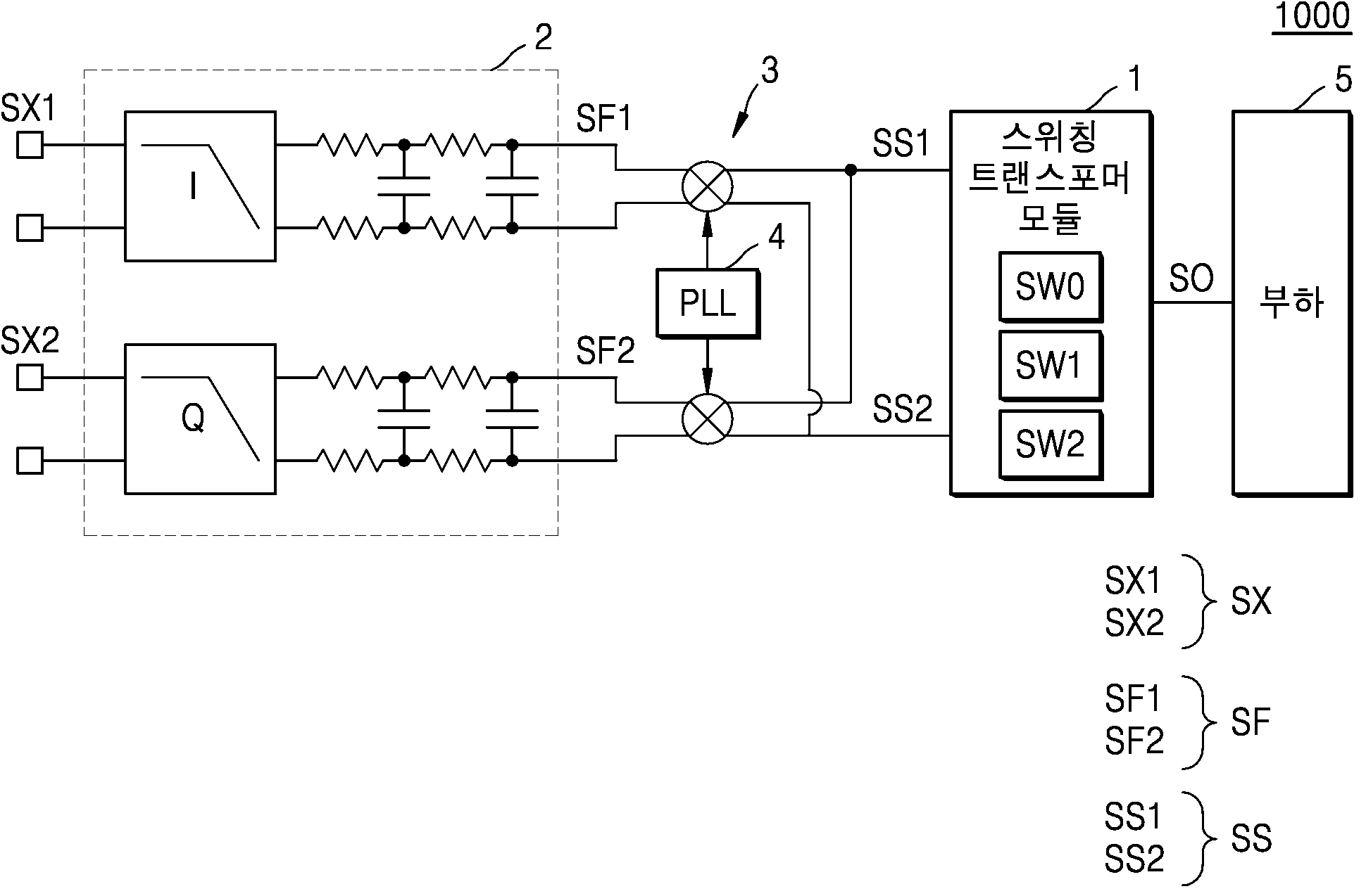
도 1을 참조하면, 전자 시스템(1000)은 스위칭 트랜스포머 모듈(1), 필터(2), 믹서(3), PLL(위상 고정 루프)(4) 및 부하(5)를 포함할 수 있다. 스위칭 트랜스포머 모듈(1)은 복수의 스위치들(SW0~SW2)을 포함할 수 있다. 예컨대, 전자 시스템(1000)은 RFIC일 수 있으며, 일 예로, 전자 시스템(1000)은 RFIC의 송신기에 포함될 수 있으며, 다른 예로, 전자 시스템(1000)은 RFIC의 수신기에 포함될 수 있으나, 이하에서는 설명의 편의상 전자 시스템(1000)은 송신기에 포함되는 것으로 예시한다.Referring to FIG. 1, the electronic system (1000) may include a switching transformer module (1), a filter (2), a mixer (3), a PLL (phase locked loop) (4), and a load (5). The switching transformer module (1) may include a plurality of switches (SW0 to SW2). For example, the electronic system (1000) may be an RFIC, and as an example, the electronic system (1000) may be included in a transmitter of the RFIC, and as another example, the electronic system (1000) may be included in a receiver of the RFIC. However, for convenience of explanation, the electronic system (1000) is exemplified as being included in a transmitter below.
본 개시의 예시적 실시예에 따른 스위칭 트랜스포머 모듈(1)은 수신된 신호에 기반하여 스위칭 동작을 수행할 수 있다. 예컨대, 스위칭 트랜스포머 모듈(1)은 수신된 신호의 주파수에 기반하여 복수의 스위치들(SW0~SW2) 중 적어도 하나를 제어함으로써, 인덕턴스 및/또는 커패시턴스 값을 조절할 수 있다. 또한, 스위칭 트랜스포머 모듈(1)은 부하의 크기에 기반하여 스위칭 동작을 수행할 수 있다. 예컨대, 스위칭 트랜스포머 모듈(1)은 부하의 임피던스 값에 기반하여 복수의 스위치들(SW0~SW2) 중 적어도 하나를 제어함으로써, 인덕턴스 및/또는 커패시턴스 값을 조절할 수 있다. A switching transformer module (1) according to an exemplary embodiment of the present disclosure can perform a switching operation based on a received signal. For example, the switching transformer module (1) can control at least one of a plurality of switches (SW0 to SW2) based on a frequency of the received signal, thereby adjusting an inductance and/or capacitance value. In addition, the switching transformer module (1) can perform a switching operation based on a size of a load. For example, the switching transformer module (1) can control at least one of a plurality of switches (SW0 to SW2) based on an impedance value of the load, thereby adjusting an inductance and/or capacitance value.
전자 시스템(1000)은 부하(5)로 신호를 전송하기 위해 필터(2)의 입력단으로부터 외부 신호(SX)를 수신할 수 있다. 예컨대, 필터(2)는 차동 입력 단자를 통해 제1 외부 신호(SX1) 및 제2 외부 신호(SX2)를 수신할 수 있다. 필터(2)는 외부 신호(SX)의 크기 및/또는 위상을 제어할 수 있도록 구성된 회로일 수 있으며 예컨대, 저역 통과 필터, 대역 통과 필터 및 고역 통과 필터 중 적어도 하나를 포함하도록 구성될 수 있다. 필터(2)는 외부 신호(SX)를 필터링한 필터 신호(filtered signal)(SF)를 출력할 수 있다. 필터(2)는 차동 출력 단자를 통해 제1 필터 신호(SF1) 및 제2 필터 신호(SF2)를 출력할 수 있다. The electronic system (1000) can receive an external signal (SX) from an input terminal of the filter (2) to transmit a signal to a load (5). For example, the filter (2) can receive a first external signal (SX1) and a second external signal (SX2) through differential input terminals. The filter (2) can be a circuit configured to control the magnitude and/or phase of the external signal (SX) and can be configured to include, for example, at least one of a low-pass filter, a band-pass filter, and a high-pass filter. The filter (2) can output a filtered signal (SF) that filters the external signal (SX). The filter (2) can output a first filtered signal (SF1) and a second filtered signal (SF2) through differential output terminals.
믹서(3)는 PLL(4)에서 출력된 기준 신호를 기반으로 필터 신호(SF)를 주파수 변환 동작을 수행하고, 주파수 변환 동작에 기반한 소스 신호(SS)를 출력할 수 있다. 예컨대, 믹서(3)는 필터 신호(SF)에 대해 상향 변환(up-conversion)을 수행할 수 있으며, 상향 변환은 PLL(4)에서 출력된 기준 신호의 주파수에 기초할 수 있다. 믹서(3)는 상향 변환된 신호인 제1 소스 신호(SS1) 및 제2 소스 신호(SS2)를 출력할 수 있다.The mixer (3) can perform a frequency conversion operation on a filter signal (SF) based on a reference signal output from the PLL (4) and output a source signal (SS) based on the frequency conversion operation. For example, the mixer (3) can perform up-conversion on the filter signal (SF), and the up-conversion can be based on the frequency of the reference signal output from the PLL (4). The mixer (3) can output a first source signal (SS1) and a second source signal (SS2), which are up-converted signals.
본 개시의 예시적 실시예에 따른 스위칭 트랜스포머 모듈(1)은 소스 신호(SS)의 주파수에 기반하여, 입력 스위치(SW0)를 개방 또는 단락함으로써, 임피던스 값을 조절할 수 있다. 예컨대, 스위칭 트랜스포머 모듈(1)은 입력 임피던스를 소스 신호(SS)의 주파수를 이용하여 공진시킴으로써, 입력 임피던스 크기를 조절할 수 있다. 입력 임피던스는, 믹서(3)로부터 스위칭 트랜스포머 모듈(1)에 포함된 구동 증폭기를 바라볼 때 관측되는 임피던스를 포함할 수 있다. 이에 따라, 구동 증폭기가 증폭 동작(또는 드라이빙 동작)을 용이하게 할 수 있다. 이와 관련하여 도 2에서 후술하기로 한다.The switching transformer module (1) according to an exemplary embodiment of the present disclosure can adjust an impedance value by opening or shorting an input switch (SW0) based on the frequency of the source signal (SS). For example, the switching transformer module (1) can adjust the input impedance size by resonating the input impedance using the frequency of the source signal (SS). The input impedance can include an impedance observed when looking at the driving amplifier included in the switching transformer module (1) from the mixer (3). Accordingly, the driving amplifier can facilitate an amplifying operation (or a driving operation). This will be described later with reference to FIG. 2.
본 개시의 예시적 실시예에 따른 스위칭 트랜스포머 모듈(1)은 소스 신호(SS)의 주파수에 기반하여, 1차 스위치(SW1) 및 2차 스위치(SW2) 중 적어도 하나를 개방 또는 단락함으로써, 1차 회로 및 2차 회로의 상호 인덕터(mutual inductor)를 조절할 수 있다. 예컨대, 스위칭 트랜스포머 모듈(1)은 1차 스위치(SW1)를 단락시킴으로써 1차 회로의 인덕턴스를 감소시킬 수 있으며, 1차 스위치(SW1)는 1차 회로에 포함된 복수의 인덕터들 중 적어도 하나에 병렬로 연결될 수 있다. 2차 스위치(SW2)도 전술한 바와 유사할 수 있다. 이와 관련하여 도 4에서 후술하기로 한다.A switching transformer module (1) according to an exemplary embodiment of the present disclosure can adjust a mutual inductor of a primary circuit and a secondary circuit by opening or short-circuiting at least one of a primary switch (SW1) and a secondary switch (SW2) based on a frequency of a source signal (SS). For example, the switching transformer module (1) can reduce an inductance of a primary circuit by short-circuiting the primary switch (SW1), and the primary switch (SW1) can be connected in parallel to at least one of a plurality of inductors included in the primary circuit. The secondary switch (SW2) can also be similar to the above-described. This will be described later with reference to FIG. 4.
도 2는 본 개시의 예시적 실시예에 따른 스위칭 트랜스포머 모듈을 설명하기 위한 회로도이다.FIG. 2 is a circuit diagram illustrating a switching transformer module according to an exemplary embodiment of the present disclosure.
도 2를 참조하면, 스위칭 트랜스포머 모듈(1)은 스위칭 트랜스포머 회로(10), 구동 증폭기(20) 및 구동 입력 회로(30)를 포함할 수 있다. 구동 입력 회로(30)는 복수의 입력 인덕터들(LI1~LI3), 입력 커패시터(CI) 및 입력 스위치(SW0)를 포함할 수 있다. 한편, 전자 시스템(1000)은 제어 로직(40)을 더 포함할 수 있다.Referring to FIG. 2, the switching transformer module (1) may include a switching transformer circuit (10), a driving amplifier (20), and a driving input circuit (30). The driving input circuit (30) may include a plurality of input inductors (LI1 to LI3), an input capacitor (CI), and an input switch (SW0). Meanwhile, the electronic system (1000) may further include a control logic (40).
본 개시의 예시적 실시예에 따르면, 구동 입력 회로(30)는 구동 증폭기(20)의 입력단에 병렬로 연결될 수 있으며, 구동 입력 회로(30)는 입력 커패시터(CI) 및 입력 스위치(SW0)를 제1 제어 명령(CTR1)에 기반하여 제어할 수 있다. 구동 입력 회로(30)는 제1 제어 명령(CTR1)에 포함된 전기적 신호에 기반하여 입력 커패시터(CI)의 커패시턴스 값을 조절할 수 있다. 한편, 입력 커패시터(CI)는 복수의 커패시터 소자들을 포함하는 커패시터 뱅크로 구현될 수 있다. 입력 스위치(SW0)는 복수의 입력 인덕터들(LI1~LI3) 중 적어도 하나와 병렬로 연결될 수 있으며, 예컨대, 제2 입력 인덕터(LI2)와 병렬로 연결될 수 있다. 입력 스위치(SW0)는 제1 제어 명령(CTR1)에 포함된 전기적 신호에 기반하여 개방 또는 단락될 수 있다. 다시 말해, 제어 로직(40)은, 입력 커패시터(CI)의 커패시턴스 값 및, 입력 스위치(SW0)의 개방 또는 단락을 지시하는 제1 제어 명령(CTR1)을 구동 입력 회로(30)로 전송할 수 있다. 일 실시예에서, 소스 신호(SS)는 구동 증폭기(20)를 통하여 입력 신호(SI)로 증폭될 수 있다. 구동 입력 회로(30)는 입력 스위치(SW0)를 조절하여 복수의 입력 인덕터들(LI1 내지 LI3)의 등가 인덕턱스 값을 가변할 수 있고, 복수의 입력 인덕터들(LI1 내지 LI3)과 병렬로 연결된 입력 커패시터(CI)의 커패시턴스 값을 조절하여 구동 증폭기(20)가 바라보는 임피던스를 제어할 수 있다. 이에 따라, 스위칭 트랜스포머 회로(10)에서 적절한 부하 임피던스를 제공 받을 수 있고, 정해진 부하 임피던스에 따라서 구동 증폭기(20)의 유닛 셀이 켜져서 원하는 출력 전압을 생성할 수 있다.According to an exemplary embodiment of the present disclosure, a driving input circuit (30) may be connected in parallel to an input terminal of a driving amplifier (20), and the driving input circuit (30) may control an input capacitor (CI) and an input switch (SW0) based on a first control command (CTR1). The driving input circuit (30) may adjust a capacitance value of the input capacitor (CI) based on an electrical signal included in the first control command (CTR1). Meanwhile, the input capacitor (CI) may be implemented as a capacitor bank including a plurality of capacitor elements. The input switch (SW0) may be connected in parallel with at least one of a plurality of input inductors (LI1 to LI3), for example, may be connected in parallel with a second input inductor (LI2). The input switch (SW0) may be opened or shorted based on an electrical signal included in the first control command (CTR1). In other words, the control logic (40) can transmit a capacitance value of the input capacitor (CI) and a first control command (CTR1) instructing opening or shorting of the input switch (SW0) to the driving input circuit (30). In one embodiment, the source signal (SS) can be amplified into an input signal (SI) through the driving amplifier (20). The driving input circuit (30) can vary the equivalent inductance values of the plurality of input inductors (LI1 to LI3) by controlling the input switch (SW0), and can control the impedance seen by the driving amplifier (20) by controlling the capacitance value of the input capacitor (CI) connected in parallel with the plurality of input inductors (LI1 to LI3). Accordingly, an appropriate load impedance can be provided from the switching transformer circuit (10), and the unit cell of the driving amplifier (20) can be turned on according to the determined load impedance to generate a desired output voltage.
도 3은 본 개시의 예시적 실시예에 따른 입력 스위치의 스위칭 동작을 설명하기 위한 회로도이다.FIG. 3 is a circuit diagram for explaining the switching operation of an input switch according to an exemplary embodiment of the present disclosure.
도 2, 도 3의 (a) 및 도 3의 (b)를 참조하면, 제어 로직(40)은 소스 신호(SS)의 주파수에 따라 입력 스위치(SW0)를 개방 또는 단락시킬 수 있으며, 입력 임피던스(ZIa, ZIb)의 크기를 조정할 수 있다. Referring to FIG. 2, FIG. 3 (a) and FIG. 3 (b), the control logic (40) can open or short the input switch (SW0) according to the frequency of the source signal (SS) and adjust the size of the input impedance (ZIa, ZIb).
제어 로직(40)은 서로 병렬로 연결된 입력 커패시터(CI) 및 복수의 입력 인덕터들(LI1~LI3)을 공진시킴으로써 구동 증폭기(20)의 전력 소모를 최소화할 수 있는 임피던스 값을 만들어 줄 수 있다. 만약, 복수의 입력 인덕터들(LI1 내지 LI3)가 없이, 입력 커패시터(CI)만 존재한다면 주파수가 높아짐에 따라서 구동 증폭기(20)을 향해 바라보는 임피던스 값이 작아질 수 있다. 상기 임피던스 값이 작아짐에 따라, 입력 전류의 크기는 증가하게 되고 전력 소모를 증가시킬 수 있다. 따라서, 복수의 입력 인덕터들(LI1~LI3)과 입력 커패시터(CI)간에 공진을 발생시켜 입력 임피던스 값을 증가시킴으로써 높은 주파수에서 입력 전류가 급격하게 증가하는 것을 방지하여 전력 소모를 감소시킬 수 있다. 또한, 믹서(3) 및 구동 증폭기(20)에 병렬로 연결된 구동 입력 회로(30)의 임피던스 값이 증가함에 따라, 입력 임피던스(ZIa)의 크기는 증가할 수 있다. 증가된 입력 임피던스(ZIa)에 기반하여, 구동 증폭기(20)는 소스 신호(SS)를 효율적으로 드라이브함으로써 입력 신호(SI)를 출력할 수 있다.The control logic (40) can create an impedance value that can minimize the power consumption of the driving amplifier (20) by resonating the input capacitor (CI) and the plurality of input inductors (LI1 to LI3) connected in parallel with each other. If only the input capacitor (CI) exists without the plurality of input inductors (LI1 to LI3), the impedance value facing the driving amplifier (20) can decrease as the frequency increases. As the impedance value decreases, the size of the input current increases, which can increase the power consumption. Therefore, by generating resonance between the plurality of input inductors (LI1 to LI3) and the input capacitor (CI) to increase the input impedance value, the input current can be prevented from increasing rapidly at high frequencies, thereby reducing the power consumption. In addition, as the impedance value of the driving input circuit (30) connected in parallel with the mixer (3) and the driving amplifier (20) increases, the size of the input impedance (ZIa) can increase. Based on the increased input impedance (ZIa), the driving amplifier (20) can output the input signal (SI) by efficiently driving the source signal (SS).
도 2 및 도 3의 (a)를 참조하면, 제어 로직(40)은 소스 신호(SS)의 주파수가 기설정된 주파수보다 낮으면, 입력 스위치(SW0)를 개방시킴으로써 원하는 주파수에서 원하는 공진 임피던스를 가질 수 있게 조절된다. 예컨대, 소스 신호(SS)의 주파수는 무선 통신에 사용되는 UHB(Ultra High Band) 대역에 포함될 수 있으며, 3.3GHz 내지 4.6GHz의 대역에 포함된 주파수일 수 있다. 개방된 입력 스위치(SW0)에 응답하여, 직렬로 연결된 복수의 입력 인덕터들(LI1~LI3)에 의해 구동 입력 회로(30)의 인덕턴스의 합은 증가할 수 있다. 소스 신호(SS)의 주파수는, 구동 입력 회로(30)의 공진 주파수일 수 있다. 제어 로직(40)은 공진 주파수가 상대적으로 낮기 때문에 인덕터를 증가시킬 필요가 있으며, 공진 주파수는 아래와 같이 인덕턴스 및 커패시턴스와 반비례 관계를 갖기 때문이다.Referring to FIG. 2 and FIG. 3 (a), the control logic (40) is adjusted to have a desired resonant impedance at a desired frequency by opening the input switch (SW0) if the frequency of the source signal (SS) is lower than a preset frequency. For example, the frequency of the source signal (SS) may be included in a UHB (Ultra High Band) band used for wireless communication, and may be a frequency included in a band of 3.3 GHz to 4.6 GHz. In response to the opened input switch (SW0), the sum of the inductances of the driving input circuit (30) may increase by a plurality of input inductors (LI1 to LI3) connected in series. The frequency of the source signal (SS) may be the resonant frequency of the driving input circuit (30). The control logic (40) needs to increase the inductor because the resonant frequency is relatively low, and the resonant frequency has an inverse relationship with the inductance and capacitance as follows.
상기 수학식 1의 는 공진 주파수(즉, 소스 신호(SS)의 주파수)이며, L은 인덕턴스(예컨대, 입력 인덕터들(LI1~LI3)의 인덕턴스 합)이고, C는 커패시턴스(즉, 입력 커패시터(CI)의 커패시턴스)일 수 있다. 즉, 인덕턱스를 증가시켜 구동 입력 회로(30)의 공진이 소스 신호(SS)의 주파수에서 발생할 수 있도록 제어할 수 있다. 상기 입력 스위치(SW0)를 제어함으로써 인덕턱스 값을 조정하는 것은 코어스 튜닝(coarse tuning)으로 지칭될 수 있다.In the above
제어 로직(40)은, 입력 스위치(SW0)를 개방함으로써 구동 입력 회로(30)의 인덕턴스를 증가시킨 이후, 입력 커패시터(CI)의 커패시턴스를 조절할 수 있다. 예컨대, 구동 입력 회로(30)가 갖는 주파수 범위를 세밀하게 조절해주기 위해, 제어 로직(40)은 커패시턴스를 조정함으로써 파인 튜닝(fine tuning)을 수행할 수 있다. 즉, 제어 로직(40)은 입력 스위치(SW0)의 개방 또는 단락을 통해 인덕턴스를 큰 범위에서 조절하여 상기 코어스 튜닝을 수행하고, 입력 커패시터(CI)의 커패시턴스를 조절함으로써 작은 범위에서 조절하여 상기 파인 튜닝을 수행할 수 있다. 예를 들어, 상기 코어스 튜닝은 큰 범위에서 인덕턴스를 제어함으로써 상기 공진 주파수를 다른 밴드의 주파수로 이동하는 것을 위한 것이며, 상기 파인 튜닝은 상기 다른 밴드의 주파수로 이동한 이후에,상기 공진 주파수를 상기 밴드 내에서 원하는 주파수로 이동하기 위한 것일 수 있다. 등가 인덕턴스를 미세하게 조절하기 위해서는 직렬로 연결된 복수의 입력 인덕터들(LI1 내지 LI3)에 스위치가 많이 붙어야 수행할 수 있으나, 이는 전력소모의 증가를 가져오게 되므로 인덕턴스를 조정하는 코어스 튜닝으로 큰 주파수 범위를 먼저 조절한 후에 가변 캐패시턴스로 미세한 주파수 범위에 접근하기 위한 파인 튜닝을 수행할 수 있다.The control logic (40) can adjust the capacitance of the input capacitor (CI) after increasing the inductance of the driving input circuit (30) by opening the input switch (SW0). For example, in order to finely adjust the frequency range of the driving input circuit (30), the control logic (40) can perform fine tuning by adjusting the capacitance. That is, the control logic (40) can perform the coarse tuning by adjusting the inductance in a large range by opening or shorting the input switch (SW0), and can perform the fine tuning by adjusting the capacitance of the input capacitor (CI) in a small range. For example, the coarse tuning may be for moving the resonant frequency to a frequency of another band by controlling the inductance in a large range, and the fine tuning may be for moving the resonant frequency to a desired frequency within the band after moving to the frequency of the other band. In order to finely adjust the equivalent inductance, it is necessary to attach many switches to multiple input inductors (LI1 to LI3) connected in series, but this leads to an increase in power consumption. Therefore, a large frequency range can be first adjusted by coarse tuning to adjust the inductance, and then fine tuning can be performed to approach a small frequency range with variable capacitance.
도 2 및 도 3의 (b)를 참조하면, 제어 로직(40)은 소스 신호(SS)의 주파수가 기설정된 주파수보다 같거나 높으면, 입력 스위치(SW0)를 단락시킬 수 있다. 예컨대, 소스 신호(SS)의 주파수는 무선 통신에 사용되는 eLAA(enhanced License Assisted Access) 대역에 포함될 수 있으며, 4.4GHz 내지 6GHz의 대역에 포함된 주파수일 수 있다. 단락된 입력 스위치(SW0)에 응답하여, 제2 입력 인덕터(LI2)로 전류 경로가 생성되지 않으며, 구동 입력 회로(30)의 인덕턴스의 합은 감소할 수 있다. 제어 로직(40)은 공진 주파수가 상대적으로 높기 때문에 인덕터를 감소시킬 수 있다.Referring to FIG. 2 and FIG. 3 (b), the control logic (40) can short-circuit the input switch (SW0) if the frequency of the source signal (SS) is equal to or higher than a preset frequency. For example, the frequency of the source signal (SS) can be included in an eLAA (enhanced License Assisted Access) band used for wireless communication, and can be a frequency included in a band of 4.4 GHz to 6 GHz. In response to the short-circuited input switch (SW0), a current path is not generated to the second input inductor (LI2), and the sum of the inductances of the driving input circuit (30) can be reduced. The control logic (40) can reduce the inductor because the resonant frequency is relatively high.
제어 로직(40)은, 입력 스위치(SW0)를 단락함으로써 구동 입력 회로(30)의 인덕턴스를 감소시킨 이후, 입력 커패시터(CI)의 커패시턴스를 조절할 수 있다. 예컨대, 구동 입력 회로(30)가 갖는 주파수 범위를 세밀하게 조절해주기 위해, 제어 로직(40)은 커패시턴스를 조정함으로써 파인 튜닝(fine tuning)을 수행할 수 있다.The control logic (40) can adjust the capacitance of the input capacitor (CI) after reducing the inductance of the driving input circuit (30) by short-circuiting the input switch (SW0). For example, in order to finely adjust the frequency range of the driving input circuit (30), the control logic (40) can perform fine tuning by adjusting the capacitance.
다시 도 2를 참조하면, 제어 로직(40)은 소스 신호(SS)의 주파수에 따라 입력 임피던스(ZI)를 최적화시키기 위하여 구동 입력 회로(30)의 입력 스위치(SW0)를 제어할 수 있다. 이에 따라, 소스 신호(SS)의 다양한 주파수 값을 구동 증폭기(20)가 커버할 수 있다. 구동 증폭기(20)는 소스 신호(SS)를 증폭시키고 입력 신호(SI)를 출력할 수 있으며, 스위칭 트랜스포머 회로(10)는 제2 제어 신호(CTR2)에 기반하여 전압 변환을 수행할 수 있다. 다양한 실시예에 따라, 제어 로직(40)은 룩업 테이블(look-up table, LUT)을 더 포함할 수 있다. 상기 LUT는 입력된 신호(예를 들어, 소스 신호(SS))의 주파수 대역마다 미리 결정된 제어 신호(CTR1, CTR2)의 값을 저장하는 매핑 테이블을 지칭할 수 있다. 예를 들어, 소스 신호(SS)의 주파수가 3.7GHz 대역의 n77 밴드에 상응하는 경우, 제어 로직(40)은 n77 밴드에 매핑된 제어 신호를 출력할 수 있다. 다른 예를 들어, 소스 신호(SS)의 주파수가 4.7GHz 대역의 n79 밴드에 상응하는 경우, 제어 로직(40)는 n79 밴드에 매핑된 제어 신호를 출력할 수 있다. 이 때, 주파수가 n77 밴드일 때 출력되는 제어 신호는 주파수가 n79 밴드일 때보다 상대적으로 낮은 주파수에서 공진을 발생시켜야 하기 때문에, 공진 입력 회로(30)의 입력 스위치(SW0)를 개방할 것을 지시하는 정보를 포함할 수 있다.Referring back to FIG. 2, the control logic (40) may control the input switch (SW0) of the driving input circuit (30) to optimize the input impedance (ZI) according to the frequency of the source signal (SS). Accordingly, the driving amplifier (20) may cover various frequency values of the source signal (SS). The driving amplifier (20) may amplify the source signal (SS) and output the input signal (SI), and the switching transformer circuit (10) may perform voltage conversion based on the second control signal (CTR2). According to various embodiments, the control logic (40) may further include a look-up table (LUT). The LUT may refer to a mapping table that stores values of predetermined control signals (CTR1, CTR2) for each frequency band of an input signal (e.g., the source signal (SS)). For example, when the frequency of the source signal (SS) corresponds to the n77 band of the 3.7 GHz band, the control logic (40) can output a control signal mapped to the n77 band. As another example, when the frequency of the source signal (SS) corresponds to the n79 band of the 4.7 GHz band, the control logic (40) can output a control signal mapped to the n79 band. At this time, since the control signal output when the frequency is the n77 band must generate resonance at a relatively lower frequency than when the frequency is the n79 band, it can include information instructing to open the input switch (SW0) of the resonance input circuit (30).
도 4는 본 개시의 예시적 실시예에 따른 스위칭 트랜스포머 회로를 설명하기 위한 블록도이다.FIG. 4 is a block diagram illustrating a switching transformer circuit according to an exemplary embodiment of the present disclosure.
도 4를 참조하면, 스위칭 트랜스포머 회로(10)는 결합계수 k에 기반하여 전기적으로 상호 결합된 1차 회로(110) 및 2차 회로(120)를 포함할 수 있으며, 1차 회로(110)는 1차 스위치(SW1)를 포함할 수 있고, 2차 회로(120)는 2차 스위치(SW2)를 포함할 수 있다.Referring to FIG. 4, a switching transformer circuit (10) may include a primary circuit (110) and a secondary circuit (120) that are electrically coupled to each other based on a coupling coefficient k, and the primary circuit (110) may include a primary switch (SW1), and the secondary circuit (120) may include a secondary switch (SW2).
구동 증폭기(20)는 입력 신호(SI)를 1차 회로(110)에 제공할 수 있다. 1차 회로(110)는 입력 신호(SI)에 기반하여 자속을 유도시킬 수 있으며, 2차 회로(120)는 유도된 자속에 기반하여 출력 신호(SO)를 출력할 수 있다. 이 경우, 제어 로직(40)은 제2 제어 신호(CTR2)를 제공함으로써, 1차 회로(110) 및 2차 회로(120) 각각의 인덕턴스를 조절하는 1차 스위치(SW1) 및 2차 스위치(SW2)를 단락 또는 개방시킬 수 있다. The driving amplifier (20) can provide an input signal (SI) to the primary circuit (110). The primary circuit (110) can induce a magnetic flux based on the input signal (SI), and the secondary circuit (120) can output an output signal (SO) based on the induced magnetic flux. In this case, the control logic (40) can short-circuit or open the primary switch (SW1) and the secondary switch (SW2) that control the inductance of each of the primary circuit (110) and the secondary circuit (120) by providing a second control signal (CTR2).
도 5는 본 개시의 예시적 실시예에 따른 스위칭 트랜스포머 회로를 설명하기 위한 회로도이다.FIG. 5 is a circuit diagram for explaining a switching transformer circuit according to an exemplary embodiment of the present disclosure.
도 5를 참조하면, 1차 회로(110)는 1차 입출력 단자(IT), 1차 커패시터(CP), 복수의 1차 인덕터들(LP1a, LP1b, LP2) 및 1차 스위치(SW1)를 포함할 수 있으며, 2차 회로(120)는 2차 입출력 단자(OT), 복수의 2차 인덕터들(LS1a, LS1b, LS2) 및 2차 스위치(SW2)를 포함할 수 있다.Referring to FIG. 5, the primary circuit (110) may include a primary input/output terminal (IT), a primary capacitor (CP), a plurality of primary inductors (LP1a, LP1b, LP2), and a primary switch (SW1), and the secondary circuit (120) may include a secondary input/output terminal (OT), a plurality of secondary inductors (LS1a, LS1b, LS2), and a secondary switch (SW2).
도 4 및 도 5를 참조하면, 1차 회로(110)는 1차 입출력 단자(IT)를 포함할 수 있으며, 1차 입출력 단자(IT)는 차동 입력 단자들(IT1, IT2)을 포함할 수 있다. 입력 신호(SI)는 제1 입력 신호(SI1) 및 제2 입력 신호(SI2)를 포함할 수 있고, 차동 입력 단자들(IT1, IT2)을 통해 1차 회로(110)는 제1 입력 신호(SI1) 및 제2 입력 신호(SI2)를 수신할 수 있다. 제1 입력 신호(SI1) 및 제2 입력 신호(SI2)는 각각 구동 증폭기(20)에서 증폭된 I 신호(In-phase Signal) 및 Q 신호(Quadrature-phase signal)에 대응될 수 있다. 한편, 2차 회로(120)는 2차 입출력 단자(OT)를 포함할 수 있으며, 2차 입출력 단자(OT)는 단일 출력 단자일 수 있다. 출력 신호(SO)는 싱글 엔드 신호(single-ended signal)일 수 있고, 2차 회로(120)는 2차 입출력 단자(OT)를 통해 출력 신호(SO)를 부하(5)로 출력할 수 있다.Referring to FIGS. 4 and 5, the primary circuit (110) may include a primary input/output terminal (IT), and the primary input/output terminal (IT) may include differential input terminals (IT1, IT2). The input signal (SI) may include a first input signal (SI1) and a second input signal (SI2), and the primary circuit (110) may receive the first input signal (SI1) and the second input signal (SI2) through the differential input terminals (IT1, IT2). The first input signal (SI1) and the second input signal (SI2) may correspond to an I signal (In-phase Signal) and a Q signal (Quadrature-phase signal) amplified by the driving amplifier (20), respectively. Meanwhile, the secondary circuit (120) may include a secondary input/output terminal (OT), and the secondary input/output terminal (OT) may be a single output terminal. The output signal (SO) may be a single-ended signal, and the secondary circuit (120) may output the output signal (SO) to the load (5) through the secondary input/output terminal (OT).
1차 커패시터(CP)는 1차 입출력 단자(IT)에 병렬로 연결될 수 있다. 예컨대, 1차 커패시터(CP)는 제1 1차 입출력 단자(IT1) 및 제2 1차 입출력 단자(IT2)에 병렬로 연결될 수 있다. 또한, 1차 커패시터(CP)는 1차 인덕터(LP)에 병렬로 연결될 수도 있다. 1차 커패시터(CP)는 후술할 1차 스위치(SW1) 및/또는 2차 스위치(SW2)의 스위칭 동작에 따른 인덕턴스 조정과 함께, 입력 신호(SI)의 주파수에 따라 커패시턴스가 조절되는 가변 커패시터일 수 있다. 예컨대, 제어 로직(40)은 제2 제어 신호(CTR2)에 기반하여 1차 커패시터(CP)의 커패시턴스 값을 조절할 수 있다. The primary capacitor (CP) may be connected in parallel to the primary input/output terminals (IT). For example, the primary capacitor (CP) may be connected in parallel to the first primary input/output terminal (IT1) and the second primary input/output terminal (IT2). In addition, the primary capacitor (CP) may be connected in parallel to the primary inductor (LP). The primary capacitor (CP) may be a variable capacitor whose capacitance is adjusted according to the frequency of the input signal (SI), along with inductance adjustment according to the switching operation of the primary switch (SW1) and/or the secondary switch (SW2) described later. For example, the control logic (40) may adjust the capacitance value of the primary capacitor (CP) based on the second control signal (CTR2).
도 6은 본 개시의 예시적 실시예에 따른 1차 회로를 설명하기 위함이다.FIG. 6 is intended to explain a primary circuit according to an exemplary embodiment of the present disclosure.
도 5, 도 6의 (a) 및 (b)을 참조하면, 1차 인덕터(LP)는 제1 1차 인덕터(LP1) 및 제2 1차 인덕터(LP2)를 포함할 수 있으며, 1차 회로(110)는 1차 연결 도선(LP3)을 포함할 수 있다. 2차 인덕터(LS)는 제1 2차 인덕터(LS1) 및 제2 2차 인덕터(LS2)를 포함할 수 있으며, 2차 회로(120)는 2차 연결 도선(LS3)을 포함할 수 있다. Referring to (a) and (b) of FIGS. 5 and 6, the primary inductor (LP) may include a first primary inductor (LP1) and a second primary inductor (LP2), and the primary circuit (110) may include a primary connecting wire (LP3). The secondary inductor (LS) may include a first secondary inductor (LS1) and a second secondary inductor (LS2), and the secondary circuit (120) may include a secondary connecting wire (LS3).
도 6의 (a) 및 (b)를 참조하면, 1차 인덕터(LP)는 1차 입출력 단자(IT)와 연결될 수 있으며, 1차 입출력 단자(IT)는 차동 단자인 제1 1차 입출력 단자(IT1) 및 제2 1차 입출력 단자(IT2)를 통해 입력 신호(SI)를 수신할 수 있다. 구체적으로, 1차 인덕터(LP)의 양단은 제1 1차 입출력 단자(IT1) 및 제2 1차 입출력 단자(IT2)와 전기적으로 연결될 수 있다.Referring to (a) and (b) of FIG. 6, a primary inductor (LP) can be connected to a primary input/output terminal (IT), and the primary input/output terminal (IT) can receive an input signal (SI) through a first primary input/output terminal (IT1) and a second primary input/output terminal (IT2), which are differential terminals. Specifically, both ends of the primary inductor (LP) can be electrically connected to the first primary input/output terminal (IT1) and the second primary input/output terminal (IT2).
1차 연결 도선(LP3)은 제1 1차 연결 도선(LP3a) 및 제2 1차 연결 도선(LP3b)을 포함할 수 있다. 제1 1차 연결 도선(LP3a)은 제1 1차 입출력 단자(IT1) 및 1차 스위치(SW1)의 일단과 제1 노드(N1)를 통해 전기적으로 연결될 수 있으며, 제2 1차 연결 도선(LP3b)은 제2 1차 입출력 단자(IT2) 및 1차 스위치(SW1)의 타단과 제2 노드(N2)를 통해 전기적으로 연결될 수 있다. The primary connecting wire (LP3) may include a first primary connecting wire (LP3a) and a second primary connecting wire (LP3b). The first primary connecting wire (LP3a) may be electrically connected to one end of the first primary input/output terminal (IT1) and the primary switch (SW1) through the first node (N1), and the second primary connecting wire (LP3b) may be electrically connected to the other end of the second primary input/output terminal (IT2) and the primary switch (SW1) through the second node (N2).
1차 연결 도선(LP3)은 제1 1차 인덕터(LP1)에 대해 인터 디짓(inter-digit) 구조를 가질 수 있다. 예컨대, 1차 연결 도선(LP3)은 제1 1차 인덕터(LP1)의 일측에 평행하게 연장되도록 형성됨으로써, 1차 연결 도선(LP3)은 제1 1차 인덕터(LP1)의 자속을 보강하는 방향으로 자속을 생성할 수 있다. 이로써, 1차 연결 도선(LP3)이 존재하지 않을 때 보다, 1차 회로(110) 및 2차 회로(120) 간의 결합 계수를 증가시킬 수 있다.The primary connecting wire (LP3) may have an inter-digit structure with respect to the first primary inductor (LP1). For example, the primary connecting wire (LP3) is formed to extend in parallel to one side of the first primary inductor (LP1), so that the primary connecting wire (LP3) can generate magnetic flux in a direction that reinforces the magnetic flux of the first primary inductor (LP1). Accordingly, the coupling coefficient between the primary circuit (110) and the secondary circuit (120) can be increased compared to when the primary connecting wire (LP3) does not exist.
1차 연결 도선(LP3)의 인덕턴스 값은 1차 인덕터(LP)의 인덕턴스 값과 실질적으로 동일할 수 있다. 다시 말해, 1차 연결 도선(LP3)의 인덕턴스 값은 제1 1차 인덕터(LP1) 및 제2 1차 인덕터(LP2) 각각의 인덕턴스 값을 합친 것과 실질적으로 동일할 수 있다. 한편, 1차 연결 도선(LP3)의 폭은, 1차 인덕터(LP)의 폭보다 얇을 수 있다. 예컨대, 제1 1차 인덕터(LP1) 및 제2 1차 인덕터(LP2)의 폭은 실질적으로 동일할 수 있으며, 1차 연결 도선(LP3)의 폭은 제1 1차 인덕터(LP1) 및 제2 1차 인덕터(LP2) 각각의 폭보다 얇을 수 있다. 전술한 바에 따른 1차 연결 도선(LP3)의 인덕턴스 값 및 폭에 의해 결합 계수가 증가함을 반복적인 실험을 통해 관측할 수 있었다.The inductance value of the primary connecting wire (LP3) may be substantially the same as the inductance value of the primary inductor (LP). In other words, the inductance value of the primary connecting wire (LP3) may be substantially the same as the sum of the inductance values of each of the first primary inductor (LP1) and the second primary inductor (LP2). Meanwhile, the width of the primary connecting wire (LP3) may be thinner than the width of the primary inductor (LP). For example, the widths of the first primary inductor (LP1) and the second primary inductor (LP2) may be substantially the same, and the width of the primary connecting wire (LP3) may be thinner than the widths of each of the first primary inductor (LP1) and the second primary inductor (LP2). Through repeated experiments, it was observed that the coupling coefficient increased with the inductance value and width of the primary connecting wire (LP3) as described above.
1차 연결 도선(LP3) 및 1차 인덕터(LP)는 제1 반도체 레이어상에 형성될 수 있으며, 1차 스위치(SW1)는 제1 반도체 레이어에 적층된 제2 반도체 레이어상에 형성될 수 있다. 이에 제한되지 않으며, 제1 반도체 레이어는 제2 반도체 레이어에 적층될 수도 있다. 예컨대, 1차 연결 도선(LP3) 및 1차 인덕터(LP)가 형성되는 제1 기판과 1차 스위치(SW1)가 형성되는 제2 기판은 서로 다른 층에 위치할 수 있다. 이로써, 1차 회로(110)의 부피를 감소시킬 수 있으며, 스위칭 트랜스포머 회로(10)의 집적도를 향상시킬 수 있다. 또한, 1차 연결 도선(LP3) 및 1차 인덕터(LP)는 비아 홀(via hole)을 채우는 도전성 비아 구조에 의해 서로 다른 레이어 상에 위치한 1차 스위치(SW1)와 연결될 수 있다. 비아 홀 및 도전성 비아 구조의 특정한 구조, 물질 및 전기적 특성에 본 개시의 기술적 사상이 제한되지는 않는다. The primary connecting conductor (LP3) and the primary inductor (LP) may be formed on a first semiconductor layer, and the primary switch (SW1) may be formed on a second semiconductor layer laminated on the first semiconductor layer. The present invention is not limited thereto, and the first semiconductor layer may also be laminated on the second semiconductor layer. For example, the first substrate on which the primary connecting conductor (LP3) and the primary inductor (LP) are formed and the second substrate on which the primary switch (SW1) is formed may be positioned on different layers. Accordingly, the volume of the primary circuit (110) can be reduced, and the integration degree of the switching transformer circuit (10) can be improved. In addition, the primary connecting conductor (LP3) and the primary inductor (LP) may be connected to the primary switch (SW1) positioned on different layers by a conductive via structure that fills a via hole. The technical ideas of the present disclosure are not limited to the specific structures, materials, and electrical properties of the via holes and the conductive via structures.
1차 스위치(SW1)는 입력 신호(SS)의 주파수에 기반하여 스위칭 동작(단락 또는 개방)을 수행할 수 있다. 1차 스위치(SW1)는 1차 인덕터(LP)의 일부와 연결됨으로써, 스위칭 동작에 기반하여 1차 인덕터(LP)의 인덕턴스의 합을 조절할 수 있다. 제어 로직(40)은 저장부에 저장된 입력 신호(SI)의 주파수에 관한 정보를 수신할 수 있으며, 다른 예로, 제어 로직(40)은 입력 신호(SI)의 주파수를 측정하고, 측정된 주파수에 관한 정보를 수신할 수 있다. 제어 로직(40)은 주파수에 관한 정보에 기반하여 제2 제어 신호(CTR2)를 1차 스위치(SW1)에 전송함으로써, 1차 스위치(SW1)를 단락 또는 개방할 수 있다.The primary switch (SW1) can perform a switching operation (short-circuiting or opening) based on the frequency of the input signal (SS). The primary switch (SW1) is connected to a part of the primary inductor (LP), so as to adjust the sum of the inductances of the primary inductor (LP) based on the switching operation. The control logic (40) can receive information about the frequency of the input signal (SI) stored in the storage unit, and as another example, the control logic (40) can measure the frequency of the input signal (SI) and receive information about the measured frequency. The control logic (40) can short-circuit or open the primary switch (SW1) by transmitting a second control signal (CTR2) to the primary switch (SW1) based on the information about the frequency.
도 6의 (a)를 참조하면, 제어 로직(40)은 입력 신호(SI)의 주파수가 기설정된 주파수보다 낮은 경우, 1차 스위치(SW1)를 개방할 수 있다. 개방된 1차 스위치(SW1)에 기반하여 1차 인덕터(LP)의 인덕턴스 값은 증가할 수 있다. 예컨대, 1차 스위치(SW1)가 개방됨에 따라, 유도 전류는 제1 1차 인덕터(LP1), 제2 1차 인덕터(LP2) 및 1차 연결 도선(LP3)에 흐를 수 있으며, 1차 스위치(SW1)에는 전류가 흐르지 않을 수 있다. 증가된 1차 인덕터(LP)의 인덕턴스 값에 기반하여, 상대적으로 낮은 입력 신호(SI)의 주파수에 따라 1차 회로(110)는 공진을 일으킬 수 있다. 다시 말해, 1차 커패시터(CP) 및 1차 인덕터(LP)는 입력 신호(SI)의 상대적으로 낮은 주파수에 의해 공진을 일으킬 수 있다. 한편, 1차 스위치(SW1)가 개방된 이후, 1차 회로(110)를 안정적인 공진 상태로 만들기 위해, 제어 로직(40)은 1차 커패시터(CP)의 커패시턴스 값을 조절할 수 있다. 다시 말해, 제어 로직(40)은 1차 커패시터(CP)를 이용해 파인 튜닝을 수행할 수 있다. Referring to (a) of FIG. 6, the control logic (40) may open the primary switch (SW1) when the frequency of the input signal (SI) is lower than the preset frequency. Based on the opened primary switch (SW1), the inductance value of the primary inductor (LP) may increase. For example, as the primary switch (SW1) is opened, the induced current may flow in the first primary inductor (LP1), the second primary inductor (LP2), and the primary connecting wire (LP3), and no current may flow in the primary switch (SW1). Based on the increased inductance value of the primary inductor (LP), the primary circuit (110) may resonate depending on the relatively low frequency of the input signal (SI). In other words, the primary capacitor (CP) and the primary inductor (LP) can resonate due to the relatively low frequency of the input signal (SI). Meanwhile, after the primary switch (SW1) is opened, the control logic (40) can adjust the capacitance value of the primary capacitor (CP) in order to make the primary circuit (110) into a stable resonance state. In other words, the control logic (40) can perform fine tuning using the primary capacitor (CP).
도 6의 (b)를 참조하면, 입력 신호(SI)의 주파수가 기설정된 주파수보다 같거나 높은 경우, 1차 스위치(SW1)를 단락할 수 있다. 단락된 1차 스위치(SW1)에 기반하여 1차 권선의 인덕턴스 값은 감소할 수 있다. 예컨대, 1차 스위치(SW1)가 단락됨에 따라, 유도 전류는 제1 1차 인덕터(LP1), 1차 스위치(SW1) 및 1차 연결 도선(LP3)에 흐를 수 있으며, 제2 1차 인덕터(LP2)에는 전류가 흐르지 않을 수 있다. 감소된 1차 인덕터(LP)의 인덕턴스 값에 기반하여, 상대적으로 높은 입력 신호(SI)의 주파수에 따라 1차 회로(110)는 공진을 일으킬 수 있다. 다시 말해, 1차 커패시터(CP) 및 1차 인덕터(LP)는 입력 신호(SI)의 상대적으로 높은 주파수에 의해 공진을 일으킬 수 있다. 한편, 1차 스위치(SW1)가 단락된 이후, 1차 회로(110)를 안정적인 공진 상태로 만들기 위해, 제어 로직(40)은 1차 커패시터(CP)의 커패시턴스 값을 조절할 수 있다.Referring to (b) of FIG. 6, when the frequency of the input signal (SI) is equal to or higher than a preset frequency, the primary switch (SW1) may be short-circuited. Based on the short-circuited primary switch (SW1), the inductance value of the primary winding may decrease. For example, when the primary switch (SW1) is short-circuited, the induced current may flow in the first primary inductor (LP1), the primary switch (SW1), and the primary connecting wire (LP3), and no current may flow in the second primary inductor (LP2). Based on the decreased inductance value of the primary inductor (LP), the primary circuit (110) may resonate according to the relatively high frequency of the input signal (SI). In other words, the primary capacitor (CP) and the primary inductor (LP) may resonate due to the relatively high frequency of the input signal (SI). Meanwhile, after the primary switch (SW1) is short-circuited, the control logic (40) can adjust the capacitance value of the primary capacitor (CP) to make the primary circuit (110) into a stable resonance state.
도 6의 (a) 및 (b)를 참조하면, 1차 스위치(SW1)는 1차 인덕터(LP)의 일부에 병렬로 연결될 수 있다. 구체적으로, 1차 스위치(SW1)는, 1차 인덕터(LP)의 일부 영역 및 1차 인덕터(LP)의 다른 일부 영역을 선택적으로 연결하기 위한, 1차 스위치(SW1)의 양단에 각각 스위치 입출력 단자들을 포함할 수 있다. 일 예로, 1차 스위치(SW1)는 제1 노드(N1) 및 제2 노드(N2)를 통해 1차 연결 도선(LP3)과 연결될 수 있으며, 1차 스위치(SW1)는 제3 노드(N3) 및 제4 노드(N4)를 통해 제1 1차 권선(LP1) 및 제2 1차 권선(LP2)과 연결될 수 있다. 한편, 전술한 바와 같이 복수의 노드들(N1~N4)은 비아 홀을 통해 형성되는 도전성 비아 구조에 의해 형성된 전기적인 노드일 수 있다.Referring to (a) and (b) of FIG. 6, the primary switch (SW1) may be connected in parallel to a portion of the primary inductor (LP). Specifically, the primary switch (SW1) may include switch input/output terminals at each end of the primary switch (SW1) for selectively connecting a portion of the primary inductor (LP) and another portion of the primary inductor (LP). For example, the primary switch (SW1) may be connected to the primary connecting wire (LP3) through the first node (N1) and the second node (N2), and the primary switch (SW1) may be connected to the first primary winding (LP1) and the second primary winding (LP2) through the third node (N3) and the fourth node (N4). Meanwhile, as described above, the plurality of nodes (N1 to N4) may be electrical nodes formed by a conductive via structure formed through a via hole.
도 7은 본 개시의 예시적 실시예에 따른 스택 스위치를 설명하기 위한 회로도이다.FIG. 7 is a circuit diagram illustrating a stack switch according to an exemplary embodiment of the present disclosure.
도 7을 참조하면, 스택 스위치(SWS)는 복수의 트랜지스터들(TR1~TR3) 및 복수의 저항들(RG, RS, RB)을 포함할 수 있다. 전술한 도면들과 함께 설명한 입력 스위치(SW0), 1차 스위치(SW1) 및 2차 스위치(SW2) 중 적어도 하나는 스택 스위치(SWS)로 구현될 수 있다. 예컨대, 1차 스위치(SW1) 및 2차 스위치(SW2)는 송신기의 큰 파워(예컨대, 구동 증폭기(20)가 출력하는 큰 파워)에 신뢰성을 가져야 할 필요가 있기 때문에, 1차 스위치(SW1) 및 2차 스위치(SW2)는 스택 스위치(SWS)로 구현될 수 있다.Referring to FIG. 7, the stack switch (SWS) may include a plurality of transistors (TR1 to TR3) and a plurality of resistors (RG, RS, RB). At least one of the input switch (SW0), the primary switch (SW1) and the secondary switch (SW2) described with the drawings described above may be implemented as the stack switch (SWS). For example, since the primary switch (SW1) and the secondary switch (SW2) need to be reliable against the large power of the transmitter (e.g., the large power output by the driving amplifier (20)), the primary switch (SW1) and the secondary switch (SW2) may be implemented as the stack switch (SWS).
복수의 트랜지스터들(TR1~TR3) 각각은 인에이블 신호(EN)가 게이트 단자로 인가될 수 있으며, 구동 전압(VDD)이 바디 단자로 인가될 수 있다. 인에이블 신호(EN) 및 구동 전압(VDD)에 응답하여 복수의 트랜지스터들(TR1~TR3)은 개방되거나 단락될 수 있다. 인에이블 신호(EN)는 전술한 제1 제어 신호(CTR1) 및 제2 제어 신호(CTR2) 중 적어도 하나에 포함될 수 있다. Each of the plurality of transistors (TR1 to TR3) can have an enable signal (EN) applied to a gate terminal and a driving voltage (VDD) applied to a body terminal. The plurality of transistors (TR1 to TR3) can be opened or shorted in response to the enable signal (EN) and the driving voltage (VDD). The enable signal (EN) can be included in at least one of the first control signal (CTR1) and the second control signal (CTR2) described above.
복수의 트랜지스터들(TR1~TR3) 각각은 소스/드레인 단자를 통해 서로 직렬로 연결될 수 있다. 예컨대, 3개의 트랜지스터들(TR1~TR3)은 서로 직렬로 연결되는 경우, 스택 스위치(SWS)는 3-스택 스위치(3-stack switch)로 칭할 수 있다. 예컨대, 제1 트랜지스터(TR1)의 소스 단자는 제2 트랜지스터(TR2)의 드레인 단자와 연결될 수 있으며, 제2 트랜지스터(TR2)의 소스 단자는 제3 트랜지스터(TR3)의 드레인 단자와 연결될 수 있다. 한편, 제1 트랜지스터(TR1)의 드레인 단자는 스택 스위치(SWS)의 일 단(T1)과 연결될 수 있으며, 제3 트랜지스터(TR3)의 소스 단자는 스택 스위치(SWS)의 타 단(T2)과 연결될 수 있다. 복수의 단자들(T1, T2)은 각각 1차 인덕터(LP)의 일부에 연결될 수 있으며, 2차 인덕터(LS)의 일부에 연결될 수 있고, 제2 입력 인덕터(LI2)와 병렬로 연결될 수도 있다.Each of the plurality of transistors (TR1 to TR3) may be connected in series with each other via source/drain terminals. For example, when three transistors (TR1 to TR3) are connected in series with each other, the stack switch (SWS) may be referred to as a 3-stack switch. For example, the source terminal of the first transistor (TR1) may be connected to the drain terminal of the second transistor (TR2), and the source terminal of the second transistor (TR2) may be connected to the drain terminal of the third transistor (TR3). Meanwhile, the drain terminal of the first transistor (TR1) may be connected to one terminal (T1) of the stack switch (SWS), and the source terminal of the third transistor (TR3) may be connected to the other terminal (T2) of the stack switch (SWS). The plurality of terminals (T1, T2) may each be connected to a portion of the primary inductor (LP), may be connected to a portion of the secondary inductor (LS), and may also be connected in parallel with the second input inductor (LI2).
도 8은 본 개시의 예시적 실시예에 따른 2차 회로를 설명하기 위함이며, 도 9는 도 8에서 2차 연결 도선이 더 포함된 2차 회로를 설명하기 위함이다. FIG. 8 is intended to explain a secondary circuit according to an exemplary embodiment of the present disclosure, and FIG. 9 is intended to explain a secondary circuit including a secondary connecting wire further in FIG. 8.
도 8을 참조하면, 2차 회로(120)는 2차 입출력 단자(OT)와 연결된 2차 인덕터(LS)를 포함할 수 있다. 2차 스위치(SW2)는 제2 제어 신호(CTR2)에 기반하여 스위칭 동작을 수행할 수 있다. 2차 스위치(SW2)는 2차 권선의 적어도 일부와 연결됨으로써, 스위칭 동작에 기반하여 2차 권선의 인덕턴스를 조절할 수 있다. 2차 인덕터(LS)는 1차 인덕터(LP)로부터 유도된 유도 신호를 제2 입출력 단자(OT)로 출력할 수 있다. 예컨대, 2차 인덕터(LS)의 일단은 제2 입출력 단자(OT)와 연결될 수 있으며, 2차 인덕터(LS)의 타단은 접지 단자(GND)와 연결될 수 있다.Referring to FIG. 8, the secondary circuit (120) may include a secondary inductor (LS) connected to a secondary input/output terminal (OT). The secondary switch (SW2) may perform a switching operation based on a second control signal (CTR2). The secondary switch (SW2) may be connected to at least a portion of the secondary winding, thereby controlling the inductance of the secondary winding based on the switching operation. The secondary inductor (LS) may output an induced signal induced from the primary inductor (LP) to the second input/output terminal (OT). For example, one end of the secondary inductor (LS) may be connected to the second input/output terminal (OT), and the other end of the secondary inductor (LS) may be connected to a ground terminal (GND).
도 9를 참조하면, 2차 회로(120)는 2차 연결 도선(LS3)을 더 포함할 수 있으며, 2차 연결 도선(LS3)은 제1 2차 연결 도선(LS3a) 및 제2 2차 연결 도선(LS3b)을 포함할 수 있다. 2차 연결 도선(LS3)은 제1 2차 인덕터(LS1)의 일측에 평행하게 연장되도록 구성될 수 있으며, 제1 2차 인덕터(LS1)의 자속을 보강하는 방향으로 자속을 생성할 수 있다. 한편, 제1 2차 연결 도선(LS3a)은 제2 입출력 단자(OT) 및 2차 스위치(SW2)의 일 단과 전기적으로 연결될 수 있으며, 제2 2차 연결 도선(LS3b)은 접지 단자(GND) 및 2차 스위치(SW2)의 타 단과 전기적으로 연결될 수 있다. Referring to FIG. 9, the secondary circuit (120) may further include a secondary connecting wire (LS3), and the secondary connecting wire (LS3) may include a first secondary connecting wire (LS3a) and a second secondary connecting wire (LS3b). The secondary connecting wire (LS3) may be configured to extend in parallel to one side of the first secondary inductor (LS1) and may generate a magnetic flux in a direction that reinforces the magnetic flux of the first secondary inductor (LS1). Meanwhile, the first secondary connecting wire (LS3a) may be electrically connected to one end of the second input/output terminal (OT) and the secondary switch (SW2), and the second secondary connecting wire (LS3b) may be electrically connected to a ground terminal (GND) and the other end of the secondary switch (SW2).
도 4, 도 8 및 도 9를 참조하면, 2차 회로(120)는 2차 인덕터(LS)는 2차 스위치(SW2)의 스위칭 동작에 기반하여 인덕턴스가 조절될 수 있다. 제어 로직(40)은 제2 제어 신호(CTR2)를 2차 회로(120)에 전송함으로써 2차 인덕터(LS)의 인덕턴스를 조절할 수 있다. 제어 로직(40)은 부하(5)의 임피던스 크기가 기설정된 값보다 작은 경우, 2차 스위치(SW2)를 개방할 수 있으며, 부하(5)의 임피던스 크기가 기설정된 값보다 같거나 큰 경우, 2차 스위치(SW2)를 개방할 수 있다. Referring to FIGS. 4, 8, and 9, the secondary circuit (120) can adjust the inductance of the secondary inductor (LS) based on the switching operation of the secondary switch (SW2). The control logic (40) can adjust the inductance of the secondary inductor (LS) by transmitting a second control signal (CTR2) to the secondary circuit (120). The control logic (40) can open the secondary switch (SW2) when the impedance size of the load (5) is smaller than a preset value, and can open the secondary switch (SW2) when the impedance size of the load (5) is equal to or greater than the preset value.
2차 스위치(SW2)는 2차 인덕터(LS)의 일부에 병렬로 연결될 수 있다. 또한, 개방된 2차 스위치(SW2)에 기반하여 2차 인덕터(LS)의 인덕턴스 값은 증가할 수 있다. 예컨대, 도 8의 (a)를 참조하면, 제1 2차 권선(LS1) 및 제2 2차 권선(LS2) 모두에 유도 전류가 흐를 수 있으며, 도 9의 (a)를 참조하면, 제1 2차 권선(LS1), 제2 2차 권선(LS2) 및 2차 연결 도선(LS3) 모두에 유도 전류가 흐를 수 있다. 한편, 단락된 2차 스위치(SW2)에 기반하여 2차 인덕터(LS)의 인덕턴스 값은 감소할 수 있다. 예컨대, 도 8의 (b)를 참조하면, 제1 2차 권선(LS1)에는 유도 전류가 흐를 수 있으며, 제2 2차 권선(LS2)에는 유도 전류가 흐르지 않을 수 있다. 도 9의 (a)를 참조하면, 제1 2차 권선(LS1) 및 2차 연결 도선(LS3)에는 유도 전류가 흐르지만, 제2 2차 권선(LS2)에는 유도 전류가 흐르지 않을 수 있다.The secondary switch (SW2) may be connected in parallel to a part of the secondary inductor (LS). In addition, the inductance value of the secondary inductor (LS) may increase based on the open secondary switch (SW2). For example, referring to (a) of FIG. 8, an induced current may flow in both the first secondary winding (LS1) and the second secondary winding (LS2), and referring to (a) of FIG. 9, an induced current may flow in all of the first secondary winding (LS1), the second secondary winding (LS2), and the secondary connecting wire (LS3). Meanwhile, the inductance value of the secondary inductor (LS) may decrease based on the short-circuited secondary switch (SW2). For example, referring to (b) of Fig. 8, an induced current may flow in the first secondary winding (LS1), but no induced current may flow in the second secondary winding (LS2). Referring to (a) of Fig. 9, an induced current may flow in the first secondary winding (LS1) and the secondary connecting wire (LS3), but no induced current may flow in the second secondary winding (LS2).
제어 로직(40)은 저장부에 저장된 부하(5)의 임피던스 크기에 관한 정보를 수신할 수 있으며, 다른 예로, 제어 로직(40)은 부하(5)의 임피던스 크기를 측정한 신호를 수신함으로써, 부하(5)의 임피던스 크기를 감지할 수 있다. 한편, 2차 회로(120)의 구체적인 구조와 특성은 1차 회로(110)에서 전술한 바와 동일 또는 유사하므로 생략하기로 한다.The control logic (40) can receive information about the impedance size of the load (5) stored in the storage unit, and as another example, the control logic (40) can detect the impedance size of the load (5) by receiving a signal measuring the impedance size of the load (5). Meanwhile, the specific structure and characteristics of the secondary circuit (120) are the same as or similar to those described above in the primary circuit (110), and thus will be omitted.
도 10 및 도 11은 본 개시의 예시적 실시예에 따른 1차 회로 및 2차 회로를 함께 설명하기 위함이다. FIGS. 10 and 11 are intended to illustrate a primary circuit and a secondary circuit together according to an exemplary embodiment of the present disclosure.
도 10의 (a) 및 (b)를 참조하면, 스위칭 트랜스포머 회로(10)는 도 6에서 전술한 1차 인덕터(LP) 및 1차 연결 도선(L3)을 포함할 수 있으며, 도 7에서 전술한 2차 인덕터(LS)를 포함할 수 있다. 다시 말해, 스위칭 트랜스포머 회로(10)는 1차 인덕터(LP), 1차 연결 도선(L3) 및 2차 인덕터(LS)가 서로 동일한 반도체 레이어 상에 형성될 수 있다. Referring to (a) and (b) of FIG. 10, the switching transformer circuit (10) may include the primary inductor (LP) and the primary connecting wire (L3) described above in FIG. 6, and may include the secondary inductor (LS) described above in FIG. 7. In other words, the switching transformer circuit (10) may be formed such that the primary inductor (LP), the primary connecting wire (L3), and the secondary inductor (LS) are formed on the same semiconductor layer.
도 11의 (a) 및 (b)를 참조하면, 스위칭 트랜스포머 회로(10)는 1차 인덕터(LP)를 포함할 수 있으며, 도 7에서 전술한 2차 인덕터(LS)를 포함할 수 있다. 다시 말해, 스위칭 트랜스포머 회로(10)는 1차 인덕터(LP) 및 2차 인덕터(LS)가 서로 동일한 반도체 레이어 상에 형성될 수 있다.Referring to (a) and (b) of FIG. 11, the switching transformer circuit (10) may include a primary inductor (LP) and may include a secondary inductor (LS) described above in FIG. 7. In other words, the switching transformer circuit (10) may be formed with the primary inductor (LP) and the secondary inductor (LS) on the same semiconductor layer.
도 10의 (a) 및 도 11의 (a)를 참조하면, 입력 신호(SI)의 주파수가 기설정된 주파수보다 낮은 경우, 1차 스위치(SW1)는 개방될 수 있으며, 1차 회로(110)의 인덕턴스는 증가할 수 있다. 또한, 부하(5)의 크기가 기설정된 크기보다 작은 경우, 2차 스위치(SW2)는 개방될 수 있으며, 2차 회로(120)의 인덕턴스는 증가할 수 있다. 도 10의 (a)를 참조하면, 스위칭 트랜스포머(10)는 1차 연결 도선(LP3)의 자속 보강으로 인해 1차 인덕터(LP) 및 2차 인덕터(LS) 간의 결합 계수(예컨대, 0.64)가 증가할 수 있다. 도 11의 (a)를 참조하면, 스위칭 트랜스포머(10)는 1차 연결 도선(LP3)의 부재로 인해 결합 계수(예컨대, 0.63)가 감소할 수 있다.Referring to (a) of FIG. 10 and (a) of FIG. 11, when the frequency of the input signal (SI) is lower than the preset frequency, the primary switch (SW1) may be opened, and the inductance of the primary circuit (110) may increase. In addition, when the size of the load (5) is smaller than the preset size, the secondary switch (SW2) may be opened, and the inductance of the secondary circuit (120) may increase. Referring to (a) of FIG. 10, the switching transformer (10) may increase the coupling coefficient (e.g., 0.64) between the primary inductor (LP) and the secondary inductor (LS) due to the magnetic flux reinforcement of the primary connecting wire (LP3). Referring to (a) of Fig. 11, the coupling coefficient (e.g., 0.63) of the switching transformer (10) may be reduced due to the absence of the primary connecting conductor (LP3).
도 10의 (b) 및 도 11의 (b)를 참조하면, 입력 신호(SI)의 주파수가 기설정된 주파수보다 높은 경우, 1차 스위치(SW1)는 단락될 수 있으며, 1차 회로(110)의 인덕턴스는 감소할 수 있다. 또한, 부하(5)의 크기가 기설정된 크기보다 같거나 큰 경우, 2차 스위치(SW2)는 단락될 수 있으며, 2차 회로(120)의 인덕턴스는 감소할 수 있다.도 10의 (b)를 참조하면, 스위칭 트랜스포머(10)는 1차 연결 도선(LP3)의 자속 보강으로 인해 1차 인덕터(LP) 및 2차 인덕터(LS) 간의 결합 계수(예컨대, 0.65)가 증가할 수 있다. 도 11의 (b)를 참조하면, 스위칭 트랜스포머(10)는 1차 연결 도선(LP3)의 부재로 인해 결합 계수(예컨대, 0.53)가 감소할 수 있다.Referring to (b) of FIG. 10 and (b) of FIG. 11, when the frequency of the input signal (SI) is higher than the preset frequency, the primary switch (SW1) may be short-circuited, and the inductance of the primary circuit (110) may decrease. In addition, when the size of the load (5) is equal to or larger than the preset size, the secondary switch (SW2) may be short-circuited, and the inductance of the secondary circuit (120) may decrease. Referring to (b) of FIG. 10, the coupling coefficient (e.g., 0.65) between the primary inductor (LP) and the secondary inductor (LS) of the switching transformer (10) may increase due to the magnetic flux reinforcement of the primary connecting wire (LP3). Referring to (b) of Fig. 11, the coupling coefficient (e.g., 0.53) of the switching transformer (10) may be reduced due to the absence of the primary connecting conductor (LP3).
도 12a 내지 도 12d는 본 개시의 예시적 실시예에 따른 1차 스위치 및 2차 스위칭 동작에 따른 1차 회로 및 2차 회로의 회로도이다. FIGS. 12A to 12D are circuit diagrams of primary circuits and secondary circuits according to primary switch and secondary switching operations according to exemplary embodiments of the present disclosure.
도 12a를 참조하면, 입력 신호(SI)의 주파수가 기설정된 주파수보다 낮을 수 있으며, 1차 스위치(SW1)는 개방될 수 있다. 또한, 부하(5)의 크기가 기설정된 값보다 작은 경우, 2차 스위치(SW2)는 개방될 수 있다. 개방된 1차 스위치(SW1)에 응답하여, 1차 스위치(SW1)에는 전류가 흐르지 않으며, 제2 1차 인덕터(LP2)에는 전류가 흐를 수 있다. 또한, 1차 회로(110)의 인덕턴스 값은, 제1 1차 인덕터(LP1), 제2 1차 인덕터(LP2) 및 1차 연결 도선(LP3)에 기반하여 상대적으로 클 수 있다. 또한, 개방된 2차 스위치(SW2)에 응답하여, 2차 스위치(SW2)에는 전류가 흐르지 않으며, 제2 2차 인덕터(LS2)에는 전류가 흐를 수 있다. 또한, 2차 회로(120)의 인덕턴스 값은, 제1 2차 인덕터(LS1), 제2 2차 인덕터(LS2) 및 2차 연결 도선(LS3)에 기반하여 상대적으로 클 수 있다.Referring to FIG. 12a, the frequency of the input signal (SI) may be lower than a preset frequency, and the primary switch (SW1) may be opened. In addition, when the size of the load (5) is smaller than a preset value, the secondary switch (SW2) may be opened. In response to the opened primary switch (SW1), no current flows through the primary switch (SW1), and current may flow through the second primary inductor (LP2). In addition, the inductance value of the primary circuit (110) may be relatively large based on the first primary inductor (LP1), the second primary inductor (LP2), and the primary connecting wire (LP3). In addition, in response to the opened secondary switch (SW2), no current flows through the secondary switch (SW2), and current may flow through the second secondary inductor (LS2). Additionally, the inductance value of the secondary circuit (120) may be relatively large based on the first secondary inductor (LS1), the second secondary inductor (LS2), and the secondary connecting wire (LS3).
도 12b를 참조하면, 입력 신호(SI)의 주파수가 기설정된 주파수보다 낮을 수 있으며, 1차 스위치(SW1)는 개방될 수 있다. 전술한 바와 같이, 1차 회로(110)의 인덕턴스 값은 상대적으로 클 수 있다. 또한, 부하(5)의 크기가 기설정된 값보다 같거나 큰 경우, 2차 스위치(SW2)는 단락될 수 있다. 단락된 2차 스위치(SW2)에 응답하여, 2차 스위치(SW2)에는 전류가 흐르며, 제2 2차 인덕터(LS2)에는 전류가 흐르지 않을 수 있다. 또한, 2차 회로(120)의 인덕턴스 값은, 제1 2차 인덕터(LS1) 및 2차 연결 도선(LS3)에 기반하여 상대적으로 작을 수 있다.Referring to FIG. 12b, the frequency of the input signal (SI) may be lower than the preset frequency, and the primary switch (SW1) may be opened. As described above, the inductance value of the primary circuit (110) may be relatively large. In addition, when the size of the load (5) is equal to or greater than the preset value, the secondary switch (SW2) may be short-circuited. In response to the short-circuited secondary switch (SW2), current may flow in the secondary switch (SW2), and no current may flow in the second secondary inductor (LS2). In addition, the inductance value of the secondary circuit (120) may be relatively small based on the first secondary inductor (LS1) and the secondary connecting wire (LS3).
도 12c를 참조하면, 입력 신호(SI)의 주파수가 기설정된 주파수보다 높을 수 있으며, 1차 스위치(SW1)는 단락될 수 있다. 단락된 1차 스위치(SW1)에 응답하여, 1차 스위치(SW1)에는 전류가 흐르며, 제2 1차 인덕터(LP2)에는 전류가 흐르지 않을 수 있다. 또한, 1차 회로(110)의 인덕턴스 값은, 제1 1차 인덕터(LP1) 및 1차 연결 도선(LP3)에 기반하여 상대적으로 작을 수 있다. 한편, 전술한 바와 같이, 부하(5)의 크기가 기설정된 값보다 작은 경우, 2차 스위치(SW2)는 개방될 수 있으며, 2차 회로(120)의 인덕턴스 값은, 제1 2차 인덕터(LS1), 제2 2차 인덕터(LS2) 및 2차 연결 도선(LS3)에 기반하여 상대적으로 클 수 있다.Referring to FIG. 12c, the frequency of the input signal (SI) may be higher than a preset frequency, and the primary switch (SW1) may be short-circuited. In response to the short-circuited primary switch (SW1), current may flow in the primary switch (SW1), and no current may flow in the second primary inductor (LP2). In addition, the inductance value of the primary circuit (110) may be relatively small based on the first primary inductor (LP1) and the primary connecting wire (LP3). Meanwhile, as described above, when the size of the load (5) is smaller than the preset value, the secondary switch (SW2) may be opened, and the inductance value of the secondary circuit (120) may be relatively large based on the first secondary inductor (LS1), the second secondary inductor (LS2), and the secondary connecting wire (LS3).
도 12d를 참조하면, 입력 신호(SI)의 주파수가 기설정된 주파수보다 높을 수 있으며, 부하(5)의 크기가 기설정된 값보다 클 수 있다. 이 경우, 1차 스위치(SW1) 및 2차 스위치(SW2)가 각각 단락됨에 응답하여, 1차 회로(110) 및 2차 회로(120 각각의 인덕턴스는 상대적으로 작을 수 있다.Referring to FIG. 12d, the frequency of the input signal (SI) may be higher than a preset frequency, and the size of the load (5) may be larger than a preset value. In this case, in response to the primary switch (SW1) and the secondary switch (SW2) being short-circuited, the inductances of the primary circuit (110) and the secondary circuit (120) may be relatively small, respectively.
도 13은 본 개시의 예시적 실시예에 따른 통신 장치를 설명하기 위한 블록도이다.FIG. 13 is a block diagram illustrating a communication device according to an exemplary embodiment of the present disclosure.
도 13을 참조하면, 통신 장치(600)는 ASIC(Application Specific Integrated Circuit)(610), ASIP(Application Specific Instruction set Processor)(630), 메모리(650), 메인 프로세서(670) 및 메인 메모리(690)를 포함할 수 있다. ASIC(610), ASIP(630) 및 메인 프로세서(670) 중 2개 이상은 상호 통신할 수 있다. 또한, ASIC(610), ASIP(630), 메모리(650), 메인 프로세서(670) 및 메인 메모리(690) 중 적어도 2개 이상은 하나의 칩에 내장될 수 있다. Referring to FIG. 13, the communication device (600) may include an ASIC (Application Specific Integrated Circuit) (610), an ASIP (Application Specific Instruction set Processor) (630), a memory (650), a main processor (670), and a main memory (690). Two or more of the ASIC (610), the ASIP (630), and the main processor (670) may communicate with each other. In addition, at least two or more of the ASIC (610), the ASIP (630), the memory (650), the main processor (670), and the main memory (690) may be embedded in one chip.
ASIP(630)은 특정한 용도를 위하여 커스텀화된 집적 회로로서, 특정 어플리케이션을 위한 전용의 명령어 세트(instruction set)를 지원할 수 있고, 명령어 세트에 포함된 명령어를 실행할 수 있다. 메모리(650)는 ASIP(630)와 통신할 수 있고, 비일시적인 저장장치로서 ASIP(630)에 의해서 실행되는 복수의 명령어들을 저장할 수도 있다. 예를 들면, 메모리(650)는, 비제한적인 예시로서 RAM(Random Access Memory), ROM(Read Only Memory), 테이프, 자기디스크, 광학디스크, 휘발성 메모리, 비휘발성 메모리 및 이들의 조합과 같이, ASIP(630)에 의해서 접근가능한 임의의 유형의 메모리를 포함할 수 있다.ASIP (630) is an integrated circuit customized for a specific purpose, and can support a dedicated instruction set for a specific application and execute instructions included in the instruction set. Memory (650) can communicate with ASIP (630) and, as a non-transitory storage device, can store a plurality of instructions executed by ASIP (630). For example, memory (650) can include any type of memory accessible by ASIP (630), such as non-limiting examples such as RAM (Random Access Memory), ROM (Read Only Memory), tape, magnetic disk, optical disk, volatile memory, non-volatile memory, and combinations thereof.
메인 프로세서(670)는 복수의 명령어들을 실행함으로써 통신 장치(600)를 제어할 수 있다. 예를 들면, 메인 프로세서(670)는 ASIC(610) 및 ASIP(630)를 제어할 수도 있고, 무선 통신 네트워크를 통해서 수신된 데이터를 처리하거나 통신 장치(600)에 대한 사용자의 입력을 처리할 수도 있다. 메인 메모리(690)는 메인 프로세서(670)와 통신할 수 있고, 비일시적인 저장장치로서 메인 프로세서(670)에 의해서 실행되는 복수의 명령어들을 저장할 수도 있다. 예를 들면, 메인 메모리(690)는, 비제한적인 예시로서 RAM(Random Access Memory), ROM(Read Only Memory), 테이프, 자기디스크, 광학디스크, 휘발성 메모리, 비휘발성 메모리 및 이들의 조합과 같이, 메인 프로세서(970)에 의해서 접근가능한 임의의 유형의 메모리를 포함할 수 있다.The main processor (670) can control the communication device (600) by executing a plurality of instructions. For example, the main processor (670) can control the ASIC (610) and the ASIP (630), process data received over a wireless communication network, or process user input to the communication device (600). The main memory (690) can communicate with the main processor (670) and can store a plurality of instructions executed by the main processor (670) as a non-transitory storage device. For example, the main memory (690) can include any type of memory accessible by the main processor (970), such as, but not limited to, a Random Access Memory (RAM), a Read Only Memory (ROM), tape, a magnetic disk, an optical disk, a volatile memory, a non-volatile memory, and combinations thereof.
스위칭 트랜스포머 모듈(1), 스위칭 트랜스포머 회로(10), 구동 입력 회로(30) 및 전자 시스템(1000) 중 적어도 하나는 도 13의 통신 장치(600)의 전부 또는 일부 구성에 포함될 수 있다. 예컨대, 스위칭 트랜스포머 회로(10) 및/또는 구동 입력 회로(30)는 입력 신호를 변압시킨 출력 신호를 필요로 하는 구성에 포함될 수 있다. 또한, 스위칭 트랜스포머 회로(10) 및/또는 구동 입력 회로(30)는 입력 신호의 주파수에 따라 제어된 변압비가 필요로 하는 구성에 포함될 수 있다. 한편, 스위칭 트랜스포머 회로(10) 및/또는 구동 입력 회로(30)의 동작 방법은, 도 13의 통신 장치(600)에 포함된 구성요소들 중 적어도 하나에 의해서 수행될 수 있다. 예컨대, 도 1의 제어 로직(40)의 동작은 메모리(650)에 저장된 복수의 명령어들로서 구현될 수 있고, ASIP(630)는 메모리(650)에 저장된 복수의 명령어들을 실행함으로써 스위칭 트랜스포머 회로(10) 및/또는 구동 입력 회로(30)의 동작 방법의 단계들 중 적어도 하나를 수행할 수 있다. 일부 실시예들에서, 스위칭 트랜스포머 회로(10) 및/또는 구동 입력 회로(30)의 동작 방법의 단계들 중 적어도 하나는 논리 합성 등을 통해서 설계된 하드웨어 블록에 의해 수행될 수 있고, 그러한 하드웨어 블록이 ASIC(610)에 포함될 수도 있다. 일부 실시예들에서, 스위칭 트랜스포머 회로(10) 및/또는 구동 입력 회로(30)의 동작 방법의 단계들 중 적어도 하나는, 메인 메모리(690)에 저장된 복수의 명령어들로서 구현될 수 있고, 메인 프로세서(670)가 메인 메모리(690)에 저장된 복수의 명령어들을 실행함으로써 스위칭 트랜스포머 회로(10) 및/또는 구동 입력 회로(30)의 동작 방법의 단계들 중 적어도 하나를 수행할 수 있다.At least one of the switching transformer module (1), the switching transformer circuit (10), the driving input circuit (30), and the electronic system (1000) may be included in all or part of the configuration of the communication device (600) of FIG. 13. For example, the switching transformer circuit (10) and/or the driving input circuit (30) may be included in a configuration that requires an output signal obtained by transforming an input signal. In addition, the switching transformer circuit (10) and/or the driving input circuit (30) may be included in a configuration that requires a controlled transformation ratio according to the frequency of the input signal. Meanwhile, the operating method of the switching transformer circuit (10) and/or the driving input circuit (30) may be performed by at least one of the components included in the communication device (600) of FIG. 13. For example, the operation of the control logic (40) of FIG. 1 may be implemented as a plurality of instructions stored in the memory (650), and the ASIP (630) may perform at least one of the steps of the operating method of the switching transformer circuit (10) and/or the driving input circuit (30) by executing the plurality of instructions stored in the memory (650). In some embodiments, at least one of the steps of the operating method of the switching transformer circuit (10) and/or the driving input circuit (30) may be performed by a hardware block designed through logic synthesis or the like, and such a hardware block may be included in the ASIC (610). In some embodiments, at least one of the steps of the method of operating the switching transformer circuit (10) and/or the driving input circuit (30) may be implemented as a plurality of instructions stored in the main memory (690), and the main processor (670) may perform at least one of the steps of the method of operating the switching transformer circuit (10) and/or the driving input circuit (30) by executing the plurality of instructions stored in the main memory (690).
이상에서와 같이 도면과 명세서에서 예시적인 실시예들이 개시되었다. 본 명세서에서 특정한 용어를 사용하여 실시예들을 설명되었으나, 이는 단지 본 개시의 기술적 사상을 설명하기 위한 목적에서 사용된 것이지 의미 한정이나 청구범위에 기재된 본 개시의 범위를 제한하기 위하여 사용된 것은 아니다. 그러므로 본 기술분야의 통상의 지식을 가진 자라면 이로부터 다양한 변형 및 균등한 타 실시예가 가능하다는 점을 이해할 것이다. 따라서, 본 개시의 진정한 기술적 보호범위는 첨부된 청구범위의 기술적 사상에 의해 정해져야 할 것이다.As described above, exemplary embodiments have been disclosed in the drawings and the specification. Although specific terms have been used in the specification to describe the embodiments, these have been used only for the purpose of explaining the technical idea of the present disclosure and have not been used to limit the meaning or the scope of the present disclosure described in the claims. Therefore, those skilled in the art will understand that various modifications and equivalent other embodiments are possible from this. Accordingly, the true technical protection scope of the present disclosure should be determined by the technical idea of the appended claims.
Claims (20)
상기 입력 신호를 입력받는 1차 입출력 단자, 상기 1차 입출력 단자와 연결된 1차 인덕터, 상기 1차 입출력 단자 및 상기 1차 인덕터에 병렬로 연결되는 1차 커패시터, 스위칭 동작에 기반하여 상기 1차 인덕터의 인덕턴스를 조절하도록 구성되는 1차 스위치, 및 상기 1차 입출력 단자 및 상기 1차 스위치의 일단을 전기적으로 연결하도록 구성되는 1차 연결 도선을 포함하도록 구성되는 1차 회로; 및
상기 1차 인덕터 및 상기 연결 도선과 전기적으로 상호 결합(mutual coupling)되는 2차 회로를 포함하는 스위칭 트랜스포머.A driving amplifier that outputs an input signal that amplifies the source signal;
A primary circuit configured to include a primary input/output terminal for receiving the input signal, a primary inductor connected to the primary input/output terminal, a primary capacitor connected in parallel to the primary input/output terminal and the primary inductor, a primary switch configured to adjust the inductance of the primary inductor based on a switching operation, and a primary connecting wire configured to electrically connect one end of the primary input/output terminal and the primary switch; and
A switching transformer including a secondary circuit electrically mutually coupled with the primary inductor and the connecting conductor.
상기 입력 신호의 주파수가 기설정된 주파수보다 낮으면 상기 1차 스위치를 개방하며, 상기 입력 신호의 주파수가 기설정된 주파수보다 같거나 높으면 상기 1차 스위치를 단락하도록 상기 1차 스위치를 제어하는 제어 로직을 더 포함하는 스위칭 트랜스포머.In the first paragraph,
A switching transformer further comprising a control logic that controls the primary switch to open the primary switch when the frequency of the input signal is lower than a preset frequency, and to close the primary switch when the frequency of the input signal is equal to or higher than the preset frequency.
상기 1차 인덕터는, 개방된 상기 1차 스위치에 응답하여 인덕턴스가 증가하며, 단락된 상기 1차 스위치에 응답하여 인덕턴스가 감소하는 것을 특징으로 하는 스위칭 트랜스포머.In the second paragraph,
A switching transformer, characterized in that the inductance of the primary inductor increases in response to the primary switch being opened, and the inductance decreases in response to the primary switch being short-circuited.
상기 제어 로직은,
상기 입력 신호의 주파수에 기반하여, 상기 1차 커패시터 및 1차 회로가 서로 공진을 일으키도록, 상기 1차 커패시터의 커패시턴스를 제어하는 특징으로 하는 스위칭 트랜스포머.In the second paragraph,
The above control logic is,
A switching transformer characterized by controlling the capacitance of the primary capacitor so that the primary capacitor and the primary circuit resonate with each other based on the frequency of the input signal.
상기 1차 스위치는,
상기 1차 인덕터의 일부 영역 및 상기 1차 인덕터의 다른 일부 영역을 선택적으로 연결하도록 포함되는 스위치 입출력 단자들을 포함하는 것을 특징으로 하는 스위칭 트랜스포머.In the first paragraph,
The above primary switch is,
A switching transformer characterized by including switch input/output terminals included to selectively connect a portion of the primary inductor and another portion of the primary inductor.
상기 2차 회로는,
2차 입출력 단자, 상기 1차 회로로부터 유도된 신호를 상기 2차 입출력 단자로 출력하도록 구성되는 2차 인덕터, 스위칭 동작에 기반하여 상기 2차 인덕터의 인덕턴스를 조절하도록 구성되는 2차 스위치, 및 상기 2차 입출력 단자 및 상기 2차 스위치의 일단을 전기적으로 연결하도록 구성되는 2차 연결 도선을 포함하는 것을 특징으로 하는 스위칭 트랜스포머.In the first paragraph,
The above secondary circuit is,
A switching transformer characterized by comprising a secondary input/output terminal, a secondary inductor configured to output a signal induced from the primary circuit to the secondary input/output terminal, a secondary switch configured to adjust the inductance of the secondary inductor based on a switching operation, and a secondary connecting wire configured to electrically connect one end of the secondary input/output terminal and the secondary switch.
상기 1차 입출력 단자는, 제1 1차 입출력 단자 및 제2 1차 입출력 단자를 포함하는 차동 단자(differential terminal)를 포함하며,
상기 1차 연결 도선은, 제1 1차 연결 도선 및 제2 1차 연결 도선을 포함하고,
상기 1차 인덕터의 양단은, 상기 제1 1차 입출력 단자 및 제2 1차 입출력 단자와 전기적으로 연결되며,
상기 제1 1차 연결 도선은, 상기 제1 1차 입출력 단자 및 상기 1차 스위치의 일단과 전기적으로 연결되며, 상기 제2 1차 연결 도선은, 상기 제2 1차 입출력 단자 및 상기 1차 스위치의 타단과 전기적으로 연결되는 것을 특징으로 하는 스위칭 트랜스포머.In the first paragraph,
The above primary input/output terminal includes a differential terminal including a first primary input/output terminal and a second primary input/output terminal,
The above primary connecting conductor includes a first primary connecting conductor and a second primary connecting conductor,
The two ends of the above primary inductor are electrically connected to the first primary input/output terminal and the second primary input/output terminal,
A switching transformer, characterized in that the first primary connecting wire is electrically connected to the first primary input/output terminal and one end of the primary switch, and the second primary connecting wire is electrically connected to the second primary input/output terminal and the other end of the primary switch.
상기 1차 연결 도선의 인덕턴스 값은, 상기 1차 인덕터의 인덕턴스 값과 실질적으로 동일한 것을 특징으로 하는 스위칭 트랜스포머.In the first paragraph,
A switching transformer, characterized in that the inductance value of the primary connecting conductor is substantially the same as the inductance value of the primary inductor.
상기 1차 인덕터 및 상기 1차 연결 도선은, 제1 반도체 레이어상에 형성되며, 상기 1차 스위치는 상기 제1 반도체 레이어에 적층된 제2 반도체 레이어상에 형성되는 것을 특징으로 하는 스위칭 트랜스포머.In the first paragraph,
A switching transformer, characterized in that the primary inductor and the primary connecting wire are formed on a first semiconductor layer, and the primary switch is formed on a second semiconductor layer laminated on the first semiconductor layer.
상기 1차 인덕터 및 상기 1차 연결 도선은, 비아 홀(via hole)을 채우는 도전성 비아 구조에 의해 상기 1차 스위치와 연결되는 것을 특징으로 하는 스위칭 트랜스포머.In Article 9,
A switching transformer, characterized in that the primary inductor and the primary connecting conductor are connected to the primary switch by a conductive via structure that fills a via hole.
상기 1차 연결 도선의 폭은, 상기 1차 인덕터보다 얇은 것을 특징으로 하는 스위칭 트랜스포머.In the first paragraph,
A switching transformer, characterized in that the width of the primary connecting wire is thinner than that of the primary inductor.
상기 1차 스위치는, 각각 인에이블 신호가 게이트 단자로 인가되고 구동 전압이 바디 단자로 인가되며, 각각의 소스/드레인 단자를 통해 서로 직렬로 연결된 복수의 트랜지스터들을 포함하는 것을 특징으로 하는 스위칭 트랜스포머.In the first paragraph,
A switching transformer characterized in that the above primary switch includes a plurality of transistors, each of which has an enable signal applied to a gate terminal and a driving voltage applied to a body terminal, and each of which is connected in series with each other through its source/drain terminals.
상기 1차 스위치는, 3 개의 트랜지스터들이 각각의 소스/드레인 단자를 통해 직렬로 연결된 3-스택 스위치를 포함하는 것을 특징으로 하는 스위칭 트랜스포머.In Article 12,
A switching transformer, wherein the above primary switch comprises a 3-stack switch in which three transistors are connected in series through their respective source/drain terminals.
소스 신호를 증폭시킨 입력 신호를 출력하는 구동 증폭기;
입력 커패시터 및 입력 인덕터를 포함하며, 스위칭 동작에 기반하여 상기 입력 인덕터의 인덕턴스를 조절하도록 구성되는 입력 스위치를 포함하고, 상기 구동 증폭기의 입력단에 전기적으로 연결되는 구동 입력 회로;
상기 입력 신호를 입력받는 1차 입출력 단자, 상기 1차 입출력 단자와 연결된 1차 인덕터, 상기 1차 입출력 단자 및 상기 1차 인덕터에 병렬로 연결되는 1차 커패시터, 스위칭 동작에 기반하여 상기 1차 인덕터의 인덕턴스를 조절하도록 구성되는 1차 스위치 및, 상기 1차 입출력 단자 및 상기 1차 스위치의 일단을 전기적으로 연결하도록 구성되는 1차 연결 도선을 포함하도록 구성되는 1차 회로; 및
상기 입력 스위치 및 상기 1차 스위치의 스위칭 동작을 제어하는 제어 로직을 포함하는 전자 시스템.A mixer that performs a frequency conversion operation and outputs a source signal;
A driving amplifier that outputs an input signal that is an amplified source signal;
A driving input circuit comprising an input capacitor and an input inductor, the input switch configured to adjust the inductance of the input inductor based on a switching operation, and electrically connected to an input terminal of the driving amplifier;
A primary circuit configured to include a primary input/output terminal for receiving the input signal, a primary inductor connected to the primary input/output terminal, a primary capacitor connected in parallel to the primary input/output terminal and the primary inductor, a primary switch configured to control the inductance of the primary inductor based on a switching operation, and a primary connecting wire configured to electrically connect one end of the primary input/output terminal and the primary switch; and
An electronic system comprising control logic for controlling switching operations of the input switch and the primary switch.
상기 제어 로직은,
상기 소스 신호의 주파수가 기설정된 값보다 작은 경우, 상기 입력 인덕터의 인덕턴스가 증가하도록 상기 1차 스위치를 제어하며, 상기 소스 신호의 주파수가 기설정된 값보다 같거나 큰 경우, 상기 입력 인덕터의 인덕턴스가 감소하도록 상기 1차 스위치를 제어하는 것을 특징으로 하는 전자 시스템.In Article 14,
The above control logic is,
An electronic system characterized in that when the frequency of the source signal is less than a preset value, the primary switch is controlled to increase the inductance of the input inductor, and when the frequency of the source signal is equal to or greater than the preset value, the primary switch is controlled to decrease the inductance of the input inductor.
2차 입출력 단자, 상기 1차 회로로부터 유도된 신호를 상기 2차 입출력 단자로 출력하도록 구성되는 2차 인덕터, 스위칭 동작에 기반하여 상기 2차 인덕터의 인덕턴스를 조절하도록 구성되는 2차 스위치 및, 상기 2차 입출력 단자 및 상기 2차 스위치의 일단을 전기적으로 연결하도록 구성되는 2차 연결 도선을 포함하도록 구성되는 2차 회로를 더 포함하는 전자 시스템.In Article 14,
An electronic system further comprising a secondary circuit configured to include a secondary input/output terminal, a secondary inductor configured to output a signal induced from the primary circuit to the secondary input/output terminal, a secondary switch configured to adjust the inductance of the secondary inductor based on a switching operation, and a secondary connecting wire configured to electrically connect one end of the secondary input/output terminal and the secondary switch.
상기 제어 로직은,
상기 2차 입출력 단자에 연결된 부하의 크기에 기반하여 상기 2차 스위치의 스위칭 동작을 제어하는 것을 특징으로 하는 전자 시스템. In Article 16,
The above control logic is,
An electronic system characterized in that the switching operation of the secondary switch is controlled based on the size of the load connected to the secondary input/output terminal.
상기 제어 로직은,
상기 부하의 크기가 기설정된 값보다 작은 경우, 상기 2차 인덕터의 인덕턴스가 증가하도록 상기 2차 스위치를 제어하며, 상기 부하의 크기가 기설정된 값보다 같거나 큰 경우, 상기 2차 인덕터의 인덕턴스가 감소하도록 상기 2차 스위치를 제어하는 것을 특징으로 하는 전자 시스템.In Article 17,
The above control logic is,
An electronic system characterized in that when the size of the load is smaller than a preset value, the secondary switch is controlled to increase the inductance of the secondary inductor, and when the size of the load is equal to or greater than the preset value, the secondary switch is controlled to decrease the inductance of the secondary inductor.
상기 1차 연결 도선은,
상기 1차 입출력 단자 및 상기 1차 스위치의 일단을 전기적으로 연결하도록 구성되는 제1 1차 연결 도선; 및
상기 1차 입출력 단자 및 상기 1차 스위치의 타단을 전기적으로 연결하도록 구성되는 제2 1차 연결 도선을 더 포함하는 것을 특징으로 하는 전자 시스템.In Article 14,
The above primary connecting wire is,
A first primary connecting wire configured to electrically connect the first input/output terminal and one end of the first switch; and
An electronic system further characterized by comprising a second primary connecting wire configured to electrically connect the first input/output terminal and the other end of the first switch.
부하와 전기적으로 연결되는 2차 입출력 단자, 상기 1차 회로로부터 유도된 신호를 상기 2차 입출력 단자로 출력하도록 구성되는 2차 인덕터, 스위칭 동작에 기반하여 상기 2차 인덕터의 인덕턴스를 조절하도록 구성되는 2차 스위치, 및 상기 2차 입출력 단자 및 상기 2차 스위치의 일단을 전기적으로 연결하도록 구성되는 2차 연결 도선을 포함하며, 상기 1차 인덕터 및 상기 연결 도선과 전기적으로 상호 결합(mutual coupling)되는 2차 회로; 및
상기 입력 신호의 주파수 및 상기 부하의 크기 중 적어도 하나에 기반하여, 상기 1차 스위치 및 상기 2차 스위치 중 적어도 하나를 제어하는 제어 로직을 포함하는 전자 시스템.A primary circuit comprising: a primary input/output terminal for receiving an input signal, a primary inductor connected to the primary input/output terminal, a primary capacitor connected in parallel to the primary input/output terminal and the primary inductor, a primary switch configured to control the inductance of the primary inductor based on a switching operation, and a primary connecting wire configured to electrically connect one end of the primary input/output terminal and the primary switch;
A secondary circuit comprising a secondary input/output terminal electrically connected to a load, a secondary inductor configured to output a signal induced from the primary circuit to the secondary input/output terminal, a secondary switch configured to adjust the inductance of the secondary inductor based on a switching operation, and a secondary connecting wire configured to electrically connect one end of the secondary input/output terminal and the secondary switch, the secondary circuit being electrically mutually coupled with the primary inductor and the connecting wire; and
An electronic system comprising control logic that controls at least one of the primary switch and the secondary switch based on at least one of the frequency of the input signal and the magnitude of the load.
Priority Applications (4)
| Application Number | Priority Date | Filing Date | Title |
|---|---|---|---|
| DE102020123684.0A DE102020123684A1 (en) | 2019-10-18 | 2020-09-11 | Switching transformers and electronic systems with the same |
| US17/060,743 US11271610B2 (en) | 2019-10-18 | 2020-10-01 | Switching transformers and electronic systems including the same |
| CN202011091329.5A CN112687456A (en) | 2019-10-18 | 2020-10-13 | Switching transformer and electronic system including the same |
| TW109135711A TWI867067B (en) | 2019-10-18 | 2020-10-15 | Switching transformers and electronic systems including the same |
Applications Claiming Priority (2)
| Application Number | Priority Date | Filing Date | Title |
|---|---|---|---|
| KR20190130187 | 2019-10-18 | ||
| KR1020190130187 | 2019-10-18 |
Publications (2)
| Publication Number | Publication Date |
|---|---|
| KR20210046527A KR20210046527A (en) | 2021-04-28 |
| KR102767188B1 true KR102767188B1 (en) | 2025-02-14 |
Family
ID=75721317
Family Applications (1)
| Application Number | Title | Priority Date | Filing Date |
|---|---|---|---|
| KR1020200072600A Active KR102767188B1 (en) | 2019-10-18 | 2020-06-15 | Switching transformers and electronic systems including same |
Country Status (3)
| Country | Link |
|---|---|
| US (1) | US11271610B2 (en) |
| KR (1) | KR102767188B1 (en) |
| TW (1) | TWI867067B (en) |
Families Citing this family (4)
| Publication number | Priority date | Publication date | Assignee | Title |
|---|---|---|---|---|
| US11177988B2 (en) * | 2020-01-23 | 2021-11-16 | Shenzhen GOODIX Technology Co., Ltd. | Receiver circuits with blocker attenuating mixer |
| US11689227B1 (en) * | 2021-12-03 | 2023-06-27 | Hangzhou Geo-Chip Technology Co., Ltd. | Broadband power amplifier device and transmitter |
| US12261581B2 (en) * | 2022-07-13 | 2025-03-25 | Apple Inc. | Tunable matching network |
| KR20250041240A (en) * | 2023-09-18 | 2025-03-25 | 충남대학교산학협력단 | Balun transformer for amplifier and amplifier having the same |
Citations (2)
| Publication number | Priority date | Publication date | Assignee | Title |
|---|---|---|---|---|
| KR101266955B1 (en) * | 2012-01-31 | 2013-05-30 | 한국과학기술원 | Switched transformer |
| US20140347154A1 (en) | 2013-05-21 | 2014-11-27 | Coherent, Inc. | Interleaved planar pcb rf transformer |
Family Cites Families (9)
| Publication number | Priority date | Publication date | Assignee | Title |
|---|---|---|---|---|
| KR100187970B1 (en) | 1995-11-03 | 1999-06-01 | 곽치영 | Upconverter for personal mobile communication base station |
| US8095082B2 (en) | 2007-10-10 | 2012-01-10 | Qualcomm, Incorporated | Dual band radio frequency transmitter |
| CN106298203B (en) | 2010-11-09 | 2018-04-27 | 朴赞雄 | For offsetting the magnetic energy transfer element and power supply of electrical noise |
| US8897726B2 (en) | 2012-06-19 | 2014-11-25 | Qualcomm Incorporated | Block sharing using three-way transformers in wireless circuits |
| US9275986B2 (en) * | 2013-11-14 | 2016-03-01 | Infineon Technologies Ag | Transistor and tunable inductance |
| KR101815768B1 (en) | 2016-01-14 | 2018-01-05 | 세종대학교산학협력단 | Impedance transformer enabling wideband matching and antenna using thereof |
| KR102115113B1 (en) * | 2016-05-27 | 2020-05-25 | 가부시키가이샤 무라타 세이사쿠쇼 | High frequency filter circuit, high frequency front end circuit and communication device |
| US10491046B2 (en) | 2016-10-20 | 2019-11-26 | Taiwan Semiconductor Manufacturing Co., Ltd. | Wireless transmitter with switchable mode |
| US11398846B2 (en) * | 2019-03-08 | 2022-07-26 | Dialog Semiconductor Korea Inc. | Transceiver having antenna-connection port and FEM-connection port |
-
2020
- 2020-06-15 KR KR1020200072600A patent/KR102767188B1/en active Active
- 2020-10-01 US US17/060,743 patent/US11271610B2/en active Active
- 2020-10-15 TW TW109135711A patent/TWI867067B/en active
Patent Citations (2)
| Publication number | Priority date | Publication date | Assignee | Title |
|---|---|---|---|---|
| KR101266955B1 (en) * | 2012-01-31 | 2013-05-30 | 한국과학기술원 | Switched transformer |
| US20140347154A1 (en) | 2013-05-21 | 2014-11-27 | Coherent, Inc. | Interleaved planar pcb rf transformer |
Also Published As
| Publication number | Publication date |
|---|---|
| TWI867067B (en) | 2024-12-21 |
| US11271610B2 (en) | 2022-03-08 |
| US20210119671A1 (en) | 2021-04-22 |
| KR20210046527A (en) | 2021-04-28 |
| TW202123617A (en) | 2021-06-16 |
Similar Documents
| Publication | Publication Date | Title |
|---|---|---|
| KR102767188B1 (en) | Switching transformers and electronic systems including same | |
| US9503025B2 (en) | Power amplifier with termination circuit and resonant circuit | |
| KR101234957B1 (en) | Apparatus for controlling power with an output network | |
| JP5191559B2 (en) | Transformer power combiner | |
| US10044400B2 (en) | Complementary metal oxide semiconductor differential antenna transmit-receive switches with power combining circuitry for orthogonal frequency-division multiplexing systems | |
| RU2416132C2 (en) | Integral version of variable inductance coil | |
| US7417515B2 (en) | On-chip TX/RX antenna switching | |
| KR101529779B1 (en) | System and circuit for transmitting a radio frequency signal through a speaker coil | |
| US20140327483A1 (en) | Complementary metal oxide semiconductor power amplifier | |
| US20070205828A1 (en) | Switched mode power amplifier using lumped element impedance inverter for parallel combining | |
| WO2020053141A1 (en) | Improvements in and relating to power divider / combiner circuits | |
| US11887765B2 (en) | Switching transformers and electronic devices including the same | |
| US11482974B2 (en) | Radio-frequency amplifier | |
| US20220337204A1 (en) | High frequency amplifier | |
| CN108141179A (en) | Power amplifier | |
| CN112614674A (en) | RF transformer for converting input RF signal to output RF signal | |
| US11387801B1 (en) | Adjustable rejection circuit with tunable impedance | |
| EP2779470B1 (en) | Integrated circuit for transmitting and receiving an RF signal | |
| CN112687456A (en) | Switching transformer and electronic system including the same | |
| US11437992B2 (en) | Low-loss mm-wave CMOS resonant switch | |
| TW201517379A (en) | Antenna tuner | |
| US20250337148A1 (en) | Directional coupler, radio frequency module, and communication device | |
| JP2003318715A (en) | High-frequency switching circuit and communication apparatus | |
| WO2025047216A1 (en) | Power amplification circuit and transmission circuit equipped with the same | |
| WO2024224809A1 (en) | High-frequency module, communication device, and control method |
Legal Events
| Date | Code | Title | Description |
|---|---|---|---|
| PA0109 | Patent application |
Patent event code: PA01091R01D Comment text: Patent Application Patent event date: 20200615 |
|
| PG1501 | Laying open of application | ||
| A201 | Request for examination | ||
| PA0201 | Request for examination |
Patent event code: PA02012R01D Patent event date: 20230615 Comment text: Request for Examination of Application Patent event code: PA02011R01I Patent event date: 20200615 Comment text: Patent Application |
|
| E902 | Notification of reason for refusal | ||
| PE0902 | Notice of grounds for rejection |
Comment text: Notification of reason for refusal Patent event date: 20240322 Patent event code: PE09021S01D |
|
| E701 | Decision to grant or registration of patent right | ||
| PE0701 | Decision of registration |
Patent event code: PE07011S01D Comment text: Decision to Grant Registration Patent event date: 20241110 |
|
| PG1601 | Publication of registration |