KR102746370B1 - Flexible display device - Google Patents
Flexible display device Download PDFInfo
- Publication number
- KR102746370B1 KR102746370B1 KR1020180156316A KR20180156316A KR102746370B1 KR 102746370 B1 KR102746370 B1 KR 102746370B1 KR 1020180156316 A KR1020180156316 A KR 1020180156316A KR 20180156316 A KR20180156316 A KR 20180156316A KR 102746370 B1 KR102746370 B1 KR 102746370B1
- Authority
- KR
- South Korea
- Prior art keywords
- region
- display device
- layer
- organic light
- filling layer
- Prior art date
- Legal status (The legal status is an assumption and is not a legal conclusion. Google has not performed a legal analysis and makes no representation as to the accuracy of the status listed.)
- Active
Links
Images


Classifications
-
- H—ELECTRICITY
- H10—SEMICONDUCTOR DEVICES; ELECTRIC SOLID-STATE DEVICES NOT OTHERWISE PROVIDED FOR
- H10K—ORGANIC ELECTRIC SOLID-STATE DEVICES
- H10K59/00—Integrated devices, or assemblies of multiple devices, comprising at least one organic light-emitting element covered by group H10K50/00
-
- G—PHYSICS
- G09—EDUCATION; CRYPTOGRAPHY; DISPLAY; ADVERTISING; SEALS
- G09F—DISPLAYING; ADVERTISING; SIGNS; LABELS OR NAME-PLATES; SEALS
- G09F9/00—Indicating arrangements for variable information in which the information is built-up on a support by selection or combination of individual elements
- G09F9/30—Indicating arrangements for variable information in which the information is built-up on a support by selection or combination of individual elements in which the desired character or characters are formed by combining individual elements
- G09F9/301—Indicating arrangements for variable information in which the information is built-up on a support by selection or combination of individual elements in which the desired character or characters are formed by combining individual elements flexible foldable or roll-able electronic displays, e.g. thin LCD, OLED
Landscapes
- Physics & Mathematics (AREA)
- General Physics & Mathematics (AREA)
- Engineering & Computer Science (AREA)
- Theoretical Computer Science (AREA)
- Electroluminescent Light Sources (AREA)
- Devices For Indicating Variable Information By Combining Individual Elements (AREA)
Abstract
본 명세서는 표시장치를 개시한다. 상기 표시장치는 접힘 영영 및 비접힘 영역을 포함하고, 상기 접힘 영역에는 내구성 향상 구조를 포함할 수 있다. 일 실시예로 상기 표시장치는, 소정의 축을 따라 접힐 수 있는 하나 이상의 제1 영역 및 상기 제1 영역에 인접한 제2 영역을 구비한 베이스 층; 상기 베이스 층의 제2 영역에 적층된 박막 트랜지스터, 유기발광 소자 및 기능 층들을 포함할 수 있다. 상기 제1 영역은, 상기 제2 영역에 적층된 박막 트랜지스터, 유기발광 소자 및 기능 층들이 존재하지 않고, 그 대신 해당 공간을 채운 충진 층을 포함한다.The present specification discloses a display device. The display device includes a foldable region and a non-foldable region, and the foldable region may include a durability-enhancing structure. In one embodiment, the display device may include a base layer having at least one first region that can be folded along a predetermined axis and a second region adjacent to the first region; a thin film transistor, an organic light-emitting element, and functional layers laminated on the second region of the base layer; the first region does not include the thin film transistor, the organic light-emitting element, and the functional layers laminated on the second region, and instead includes a filling layer filling the corresponding space.
Description
본 명세서는 플렉서블 표시장치에 관한 것이다.This specification relates to a flexible display device.
다양한 정보를 화면으로 구현해 주는 영상표시장치는 정보 통신 시대의 핵심 기술로 더 얇고 더 가볍고 휴대가 가능하면서도 고성능의 방향으로 발전하고 있다. 이에 유기발광 소자의 발광량을 제어하여 영상을 표시하는 유기발광 표시장치 등이 각광받고 있다.The video display device that implements various information on the screen is a core technology of the information and communication era and is developing in the direction of thinner, lighter, more portable, and more high-performance. Accordingly, organic light-emitting display devices that control the light emission of organic light-emitting elements to display images are in the spotlight.
유기발광 소자는 전극 사이의 얇은 발광층을 이용한 자발광 소자로 박막화가 가능하다는 장점이 있다. 일반적인 유기발광 표시장치는 기판에 화소구동 회로와 유기발광 소자가 형성된 구조를 갖고, 유기발광 소자에서 방출된 빛이 기판 또는 배리어층을 통과하면서 화상을 표시하게 된다.Organic light-emitting elements are self-luminous elements that utilize a thin light-emitting layer between electrodes, and have the advantage of being able to be made thin. A typical organic light-emitting display device has a structure in which a pixel driver circuit and an organic light-emitting element are formed on a substrate, and the light emitted from the organic light-emitting element displays an image by passing through the substrate or barrier layer.
유기발광 표시장치는 별도의 광원장치 없이 구현되기 때문에, 플렉서블(flexible), 벤더블(bendable), 폴더블(foldable) 표시장치로 구현되기에 용이하다. 이때, 플라스틱, 박막 금속(metal foil) 등의 플렉서블 재료가 유기발광 표시장치의 기판으로 사용된다.Since organic light-emitting displays are implemented without a separate light source device, they are easy to implement as flexible, bendable, and foldable displays. At this time, flexible materials such as plastic and metal foil are used as substrates for organic light-emitting displays.
최근에는, 다양한 형태로 변형될 수 있는 표시장치에 대한 수요가 증가하고 있으며, 그에 따라 유기발광 표시장치를 폴더블 혹은 롤러블 표시장치로 구현하는 연구도 활발히 진행되고 있다. 그러나 종래의 폴더블 혹은 롤러블 표시장치는 구조/재료적인 특성과 한계로 인하여 개선할 부분이 여전히 많이 존재하고 있다.Recently, the demand for display devices that can be transformed into various forms is increasing, and accordingly, research on implementing organic light-emitting display devices as foldable or rollable display devices is also actively being conducted. However, conventional foldable or rollable display devices still have many areas for improvement due to structural/material characteristics and limitations.
본 명세서는 플렉서블 표시장치의 접힘 구조 및 그에 사용되는 내구성 향상 구조를 제안하는 것을 목적으로 한다.The purpose of this specification is to propose a folding structure of a flexible display device and a durability-enhancing structure used therein.
본 명세서의 과제들은 이상에서 언급한 과제들로 제한되지 않으며, 언급되지 않은 또 다른 과제들은 아래의 기재로부터 당업자에게 명확하게 이해될 수 있을 것이다.The tasks of this specification are not limited to those mentioned above, and other tasks not mentioned will be clearly understood by those skilled in the art from the description below.
본 명세서의 일 실시예에 따라 표시장치가 제공된다. 상기 표시장치는 접힘 영영 및 비접힘 영역을 포함하고, 상기 접힘 영역에는 내구성 향상 구조를 포함할 수 있다. 일 실시예로 상기 표시장치는, 소정의 축을 따라 접힐 수 있는 하나 이상의 제1 영역 및 상기 제1 영역에 인접한 제2 영역을 구비한 베이스 층; 상기 베이스 층의 제2 영역에 적층된 박막 트랜지스터, 유기발광 소자 및 기능 층들을 포함할 수 있다. 상기 제1 영역은, 상기 제2 영역에 적층된 박막 트랜지스터, 유기발광 소자 및 기능 층들이 존재하지 않고, 그 대신 해당 공간을 채운 충진 층을 포함한다.According to one embodiment of the present disclosure, a display device is provided. The display device includes a foldable region and a non-foldable region, and the foldable region may include a durability-enhancing structure. In one embodiment, the display device may include a base layer having at least one first region that can be folded along a predetermined axis and a second region adjacent to the first region; a thin film transistor, an organic light-emitting element, and functional layers stacked on the second region of the base layer; The first region does not include the thin film transistor, the organic light-emitting element, and the functional layers stacked on the second region, and instead includes a filling layer filling the corresponding space.
타 실시예의 구체적인 사항들은 상세한 설명 및 도면들에 포함되어 있다.Specific details of other embodiments are included in the detailed description and drawings.
본 명세서의 실시예들은, 폴더블 표시장치의 접힘 부분에서 발생하는 불량을 최소화하는 안정적인 구조를 제공할 수 있다. 더 나아가, 본 명세서의 실시예들은, 폴더블/롤러블 표시장치의 구조적 견고성을 강화하는 내구성 강화 구조를 제공할 수 있다. 본 명세서의 실시예들에 따른 효과는 이상에서 예시된 내용에 의해 제한되지 않으며 더욱 다양한 효과들이 본 명세서 내에 포함되어 있다.The embodiments of the present specification can provide a stable structure that minimizes defects occurring at the folding portion of a foldable display device. Furthermore, the embodiments of the present specification can provide a durability-enhanced structure that enhances the structural rigidity of a foldable/rollable display device. The effects according to the embodiments of the present specification are not limited to the contents exemplified above, and more diverse effects are included in the present specification.
도 1은 전자장치에 포함될 수 있는 예시적인 플렉서블 표시장치를 도시한다.
도 2a 내지 2c는 본 명세서의 일 실시예에 따른 플렉서블 표시장치의 평면도이다.
도 3은 도 2c의 1-1' 선을 따른 단면도이다.
도 4는 도 2c의 2-2' 선을 따른 단면도이다.
도 5a 및 5b는 본 명세서의 다른 실시예에 따른 플렉서블 표시장치의 평면도 및 단면도이다.Figure 1 illustrates an exemplary flexible display device that may be included in an electronic device.
FIGS. 2A to 2C are plan views of a flexible display device according to one embodiment of the present specification.
Figure 3 is a cross-sectional view along line 1-1' of Figure 2c.
Figure 4 is a cross-sectional view along line 2-2' of Figure 2c.
FIGS. 5A and 5B are plan and cross-sectional views of a flexible display device according to another embodiment of the present specification.
본 명세서의 이점 및 특징, 그리고 그것들을 달성하는 방법은 첨부되는 도면과 함께 상세하게 후술되어 있는 실시예들을 참조하면 명확해질 것이다. 그러나 본 발명은 이하에서 개시되는 실시예들에 한정되는 것이 아니라 서로 다른 다양한 형태로 구현될 것이며, 단지 본 실시예들은 본 발명의 개시가 완전하도록 하며, 본 발명이 속하는 기술분야에서 통상의 지식을 가진 자에게 발명의 범주를 완전하게 알려주기 위해 제공되는 것이며, 본 발명은 청구항의 범주에 의해 정의될 뿐이다.The advantages and features of the present specification and the methods for achieving them will become clearer with reference to the embodiments described in detail below together with the accompanying drawings. However, the present invention is not limited to the embodiments disclosed below, but may be implemented in various different forms, and the present embodiments are provided only to make the disclosure of the present invention complete and to fully inform those skilled in the art of the scope of the invention, and the present invention is defined only by the scope of the claims.
본 명세서의 실시예를 설명하기 위한 도면에 개시된 형상, 크기, 비율, 각도, 개수 등은 예시적인 것이므로 본 명세서가 도시된 사항에 한정되는 것은 아니다. 명세서 전체에 걸쳐 동일 참조 부호는 동일 구성 요소를 지칭한다. 또한, 본 발명을 설명함에 있어서, 관련된 공지 기술에 대한 구체적인 설명이 본 발명의 요지를 불필요하게 흐릴 수 있다고 판단되는 경우 그 상세한 설명은 생략한다. 본 명세서 상에서 언급된 '포함한다', '갖는다', '이루어진다' 등이 사용되는 경우 '~만'이 사용되지 않는 이상 다른 부분이 추가될 수 있다. 구성 요소를 단수로 표현한 경우에 특별히 명시적인 기재 사항이 없는 한 복수를 포함하는 경우를 포함한다. 구성 요소를 해석함에 있어서, 별도의 명시적 기재가 없더라도 오차 범위를 포함하는 것으로 해석한다.The shapes, sizes, ratios, angles, numbers, etc. disclosed in the drawings for explaining the embodiments of the present specification are illustrative and therefore the present specification is not limited to the matters illustrated. Like reference numerals refer to like elements throughout the specification. In addition, in describing the present invention, if it is determined that a detailed description of a related known technology may unnecessarily obscure the gist of the present invention, the detailed description will be omitted. When the terms “includes,” “has,” “consists of,” etc. are used in this specification, other parts may be added unless “only” is used. When a component is expressed in the singular, it includes a case where the plural is included unless there is a specifically explicit description. When interpreting a component, it is interpreted to include a range of errors even if there is no separate explicit description.
위치 관계에 대한 설명일 경우, 예를 들어, '~상에', '~상부에', '~하부에', '~옆에' 등으로 두 부분의 위치 관계가 설명되는 경우, '바로' 또는 '직접'이 사용되지 않는 이상 두 부분 사이에 하나 이상의 다른 부분이 위치할 수도 있다. 소자 또는 층이 다른 소자 또는 층 "위 (on)"로 지칭되는 것은 다른 소자 바로 위에 또는 중간에 다른 층 또는 다른 소자를 개재한 경우를 모두 포함한다. 어떤 구성 요소가 다른 구성요소에 "연결", "결합" 또는 "접속"된다고 기재된 경우, 그 구성 요소는 그 다른 구성요소에 직접적으로 연결되거나 또는 접속될 수 있지만, 각 구성 요소 사이에 다른 구성 요소가 "개재"되거나, 각 구성 요소가 다른 구성 요소를 통해 "연결", "결합" 또는 "접속"될 수도 있다고 이해되어야 할 것이다. When describing a positional relationship, for example, when the positional relationship between two parts is described as "on", "above", "below", "next to", etc., one or more other parts may be located between the two parts unless "directly" or "directly" is used. When an element or layer is referred to as "on" another element or layer, it includes both cases where it is directly on the other element or where another layer or other element is interposed. When it is described that a component is "connected", "coupled", or "connected" to another component, it should be understood that the component may be directly connected or connected to the other component, but it should also be understood that other components may be "interposed" between each component, or each component may be "connected", "coupled", or "connected" through the other component.
비록 제1, 제2 등이 다양한 구성요소들을 서술하기 위해서 사용되나, 이들 구성요소들은 이들 용어에 의해 제한되지 않는다. 이들 용어들은 단지 하나의 구성요소를 다른 구성요소와 구별하기 위하여 사용하는 것이다. 따라서, 이하에서 언급되는 제1 구성요소는 본 발명의 기술적 사상 내에서 제2 구성요소일 수도 있다.Although the terms first, second, etc. are used to describe various components, these components are not limited by these terms. These terms are only used to distinguish one component from another. Accordingly, a first component referred to below may also be a second component within the technical concept of the present invention.
도면에서 나타난 각 구성의 크기 및 두께는 설명의 편의를 위해 도시된 것이며, 본 발명이 도시된 구성의 크기 및 두께에 반드시 한정되는 것은 아니다. 이하, 첨부된 도면을 참조하여 본 발명의 다양한 실시예들을 상세히 설명한다.The size and thickness of each component shown in the drawings are shown for convenience of explanation, and the present invention is not necessarily limited to the size and thickness of the components shown. Hereinafter, various embodiments of the present invention will be described in detail with reference to the attached drawings.
도 1은 전자장치에 포함될 수 있는 예시적인 플렉서블 표시장치를 도시한다.Figure 1 illustrates an exemplary flexible display device that may be included in an electronic device.
상기 플렉서블(flexible) 표시장치는 가요성(flexibility)이 부여된 표시장치를 의미하는 것으로, 접을 수 있는(foldable) 표시장치, 구부릴 수 있는(bendable) 표시장치, 말수있는(rollable) 표시장치 등과 동일한 의미로 사용될 수 있다. 도 1을 참조하면, 상기 표시장치(100)는 적어도 하나의 표시 영역(active area)을 포함할 수 있다. 예컨대, 폴더블 표시장치는 굴곡 선(bending line)을 기준으로 좌우 (또는 상하)로 구분되는 다수의 표시 영역을 가질 수 있다. 상기 표시 영역에는 픽셀들의 어레이(array)가 형성된다. 하나 이상의 비표시 영역(inactive area)이 상기 표시 영역의 주위에 배치될 수 있다. 즉, 상기 비표시 영역은, 표시 영역의 하나 이상의 측면에 인접할 수 있다. 도 1에서, 상기 비표시 영역은 사각형 형태의 표시 영역을 둘러싸고 있다. 그러나, 표시 영역의 형태 및 표시 영역에 인접한 비표시 영역의 형태/배치는 도 1에 도시된 예에 한정되지 않는다. 상기 표시 영역 및 상기 비표시 영역은, 상기 표시장치(100)를 탑재한 전자장치의 디자인에 적합한 형태일 수 있다. 상기 표시 영역의 예시적 형태는 오각형, 육각형, 원형, 타원형 등이다.The flexible display device above refers to a display device with flexibility, and can be used with the same meaning as a foldable display device, a bendable display device, a rollable display device, etc. Referring to FIG. 1, the display device (100) can include at least one display area (active area). For example, the foldable display device can have a plurality of display areas divided left and right (or up and down) based on a bending line. An array of pixels is formed in the display area. One or more inactive areas can be arranged around the display area. That is, the inactive areas can be adjacent to one or more side surfaces of the display area. In FIG. 1, the inactive areas surround a rectangular display area. However, the shape of the display area and the shape/arrangement of the inactive areas adjacent to the display area are not limited to the example illustrated in FIG. 1. The above display area and the non-display area may have shapes suitable for the design of an electronic device equipped with the display device (100). Exemplary shapes of the display area include a pentagon, a hexagon, a circle, an oval, etc.
상기 표시 영역 내의 각 픽셀은 픽셀 회로와 연관될 수 있다. 상기 픽셀 회로는, 백플레인(backplane) 상의 하나 이상의 스위칭 트랜지스터 및 하나 이상의 구동 트랜지스터를 포함할 수 있다. 각 픽셀 회로는, 상기 비표시 영역에 위치한 게이트 드라이버 및 데이터 드라이버와 같은 하나 이상의 제어 회로와 통신하기 위해, 게이트 라인 및 데이터 라인과 전기적으로 연결될 수 있다.Each pixel within the display area may be associated with a pixel circuit. The pixel circuit may include one or more switching transistors and one or more driving transistors on a backplane. Each pixel circuit may be electrically connected to a gate line and a data line to communicate with one or more control circuits, such as a gate driver and a data driver, located in the non-display area.
상기 제어 회로는, 도 1에 도시된 것처럼, 상기 비표시 영역에 TFT(thin film transistor)로 구현될 수 있다. 이러한 제어 회로는 GIP(gate-in-panel)로 지칭될 수 있다. 또한, 데이터 드라이버 IC와 같은 몇몇 부품들은, 분리된 인쇄 회로 기판에 탑재되고, FPCB(flexible printed circuit board), COF(chip-on-film), TCP(tape-carrier-package) 등과 같은 회로 필름을 이용하여 상기 비표시 영역에 배치된 연결 인터페이스(패드/범프, 핀 등)와 결합될 수 있다. The above control circuit may be implemented as a TFT (thin film transistor) in the non-display area, as illustrated in FIG. 1. Such a control circuit may be referred to as a GIP (gate-in-panel). In addition, several components, such as a data driver IC, may be mounted on a separate printed circuit board and coupled to a connection interface (pad/bump, pin, etc.) placed in the non-display area using a circuit film, such as an FPCB (flexible printed circuit board), a COF (chip-on-film), a TCP (tape-carrier-package), etc.
상기 플렉서블 표시장치(100)는, 다양한 신호를 생성하거나 표시 영역내의 픽셀을 구동하기 위한, 다양한 부가 요소들 포함할 수 있다. 상기 픽셀을 구동하기 위한 부가 요소는 인버터 회로, 멀티플렉서, 정전기 방전 회로(electro static discharge) 등을 포함할 수 있다. 상기 표시장치(100)는 픽셀 구동 이외의 기능과 연관된 부가 요소도 포함할 수 있다. 예를 들어, 상기 표시장치(100)는 터치 감지 기능, 사용자 인증 기능(예: 지문 인식), 멀티 레벨 압력 감지 기능, 촉각 피드백(tactile feedback) 기능 등을 제공하는 부가 요소들을 포함할 수 있다. 상기 언급된 부가 요소들은 상기 비표시 영역 및/또는 상기 연결 인터페이스와 연결된 외부 회로에 위치할 수 있다.The flexible display device (100) may include various additional elements for generating various signals or driving pixels within a display area. Additional elements for driving the pixels may include an inverter circuit, a multiplexer, an electro static discharge circuit, etc. The display device (100) may also include additional elements associated with functions other than pixel driving. For example, the display device (100) may include additional elements that provide a touch detection function, a user authentication function (e.g., fingerprint recognition), a multi-level pressure detection function, a tactile feedback function, etc. The above-mentioned additional elements may be located in the non-display area and/or an external circuit connected to the connection interface.
상기 표시장치(100)의 여러 부분들은 굴곡선(BL)을 따라 구부러질 수 있다. 상기 굴곡선(BL)은 수평으로(예: 도 1의 X 방향), 수직으로(예: 도 1의 Y 방향), 또는 대각선으로 연장될 수 있다 따라서, 상기 표시장치(100)는, 요구되는 디자인에 기초하여, 수평, 수직, 대각선 방향의 조합으로 구부러질 수 있다.Various parts of the display device (100) can be bent along a bend line (BL). The bend line (BL) can extend horizontally (e.g., in the X direction of FIG. 1), vertically (e.g., in the Y direction of FIG. 1), or diagonally. Accordingly, the display device (100) can be bent in a combination of horizontal, vertical, and diagonal directions based on a required design.
언급한 대로, 상기 표시장치(100)의 하나 이상의 모서리(edge)는, 상기 굴곡선(BL)을 따라 중앙 부분(central portion)에서 멀어지도록 구부러질 수 있다. 상기 굴곡선(BL)은 상기 중앙 부분을 가로질러 연장되거나, 상기 표시장치(100)의 하나 이상의 꼭지점(corner)에서 대각선으로 연장될 수 있다. 이러한 구조는 상기 표시장치(100)가 폴더블(foldable) 표시장치가 되거나, 또는 접히는 양면에 표시가 이뤄지는 표시장치가 되도록 할 수 있다. 더 나아가 다수 개의 굴곡선(BL)이 촘촘히 존재함으로써 상기 표시장치는 적어도 일 부분을 말 수도(롤러블) 있다.As mentioned, one or more edges of the display device (100) may be bent away from the central portion along the curved line (BL). The curved line (BL) may extend across the central portion, or may extend diagonally from one or more corners of the display device (100). This structure may enable the display device (100) to be a foldable display device, or a display device in which displays are formed on both sides when folded. Furthermore, since a plurality of curved lines (BL) are densely present, the display device may be rollable at least at one portion.
몇몇 실시예에서 플렉서블 표시장치(100)의 굴곡 부분은, 이미지를 표시할 수 있는 표시 영역을 포함할 수 있다. 이러한 표시 영역을 보조 표시 영역이라 호칭한다. 즉, 표시 영역의 적어도 일부 픽셀이 굴곡 부분에 포함되도록 굴곡선(BL)이 표시 영역 내에 놓일 수 있다.In some embodiments, the curved portion of the flexible display device (100) may include a display area capable of displaying an image. This display area is referred to as an auxiliary display area. That is, a curved line (BL) may be placed within the display area so that at least some pixels of the display area are included in the curved portion.
도 2a 내지 2c는 본 명세서의 일 실시예에 따른 플렉서블 표시장치의 평면도이다.FIGS. 2A to 2C are plan views of a flexible display device according to one embodiment of the present specification.
이하에서는, 유기발광 표시장치(Organic Light Emitting Display)를 일 예로 하여 본 명세서의 실시예에 따른 플렉서블 표시장치 및 그 표시 영역을 설명한다. 상기 플렉서블 표시장치(100)는, 굴곡선(BL)을 따라 배치된 내구성 향상 구조를 갖는다. 상기 내구성 향상 구조를 통해 예시된 유기발광 표시장치는 접을 수 있는(폴더블), 혹은 말 수 있는(롤러블) 표시장치에 더 적합하게 사용될 수 있다.Hereinafter, a flexible display device and its display area according to an embodiment of the present specification will be described using an Organic Light Emitting Display as an example. The flexible display device (100) has a durability-enhancing structure arranged along a bending line (BL). The organic light emitting display device exemplified by the durability-enhancing structure can be more suitably used in a foldable or rollable display device.
종래의 폴더블 혹은 롤러블 표시장치는 구조/재료적인 특성과 한계로 인하여 개선할 부분이 많이 존재하였다. 대표적으로, 폴더블 혹은 롤러블 표시장치의 두께가 얇을수록 굽혀지는 곡률은 증가하지만, 굴곡 부분에 있는 무기막 또는 금속성 소자에 손상(크랙 등)이 생기고 전파되는 현상이 발견되었다. 또한 그 대응책으로 굴곡 부분을 패터닝하면 표시장치의 강성이 약해지는 문제가 있었다. 따라서, 일정 두께 이하로 표시장치를 구현하여 최대한의 유연성을 확보하는 데에는 큰 어려움이 있었다.Conventional foldable or rollable displays have many areas for improvement due to structural/material characteristics and limitations. For example, as the thickness of a foldable or rollable display device becomes thinner, the bending curvature increases, but it has been discovered that damage (cracks, etc.) occurs and propagates in the inorganic film or metallic elements in the bending portion. In addition, when the bending portion is patterned as a countermeasure, there is a problem that the rigidity of the display device is weakened. Therefore, it has been very difficult to secure maximum flexibility by implementing a display device below a certain thickness.
이에 본 명세서의 발명자들은, 폴더블 혹은 롤러블 표시장치의 접힘 반지름을 더 작게 할 수 있고, 동시에 그로 인한 강성의 저하를 예방하는 내구성 향상 구조를 고안하였다. 상기 내구성 향상 구조는 접힘 영역(B)을 따라 마련된 식각(etched) 부분과 상기 식각 부분을 채우는 충진 층을 포함할 수 있다. Accordingly, the inventors of the present specification have devised a durability-enhancing structure that can reduce the folding radius of a foldable or rollable display device and at the same time prevent a decrease in rigidity due to the reduction. The durability-enhancing structure may include an etched portion provided along a folding area (B) and a filling layer filling the etched portion.
먼저, 도 2a를 참고하면, 본 명세서의 일 실시예에 따른 표시장치의 평면도를 볼 수 있다. 도 2a는 도 1의 플렉서블 표시장치에서 상하 부분을 일부 생략한 도면과 동일하다.First, referring to Fig. 2a, a plan view of a display device according to one embodiment of the present specification can be seen. Fig. 2a is the same as the drawing of the flexible display device of Fig. 1 with some of the upper and lower portions omitted.
표시장치(100)의 표시 영역(A/A)에는 베이스 층과, 그 위에 마련된 박막 트랜지스터, 유기발광 소자 및 기능 층(절연 층, 평탄화 층 등)들이 배치될 수 있다. 상기 표시 영역(A/A) 상에는 박막트랜지스터(102, 104, 106, 108), 유기발광소자(112, 114, 116) 및 각종 기능 층(layer)이 위치하고 있다. 박막 트랜지스터는 상기 베이스 층(101)의 일 면(제1 면)에 배치된다. 상기 베이스 층(101)이 플라스틱으로 이루어진 경우, 플라스틱 필름 또는 플라스틱 기판으로 지칭될 수 있다. 유기발광 다이오드는 상기 박막 트랜지스터 상에 배치된다. 상기 유기발광 다이오드는, 베이스 층(101) 상에 구현된 픽셀 회로 및 제어 회로, 상기 베이스 층(101) 상의 연결 인터페이스와 연결된 외부의 다른 구동회로에 의해 제어된다. 상기 유기발광 다이오드는 특정 색상(예: red, green, blue)의 광을 방출하는 유기발광물질 층을 포함한다. 몇몇 실시예에서, 상기 유기발광물질 층은 백색 광(본질적으로는 여러 색상의 광의 조합)을 방출할 수 있는 적층 구조를 가질 수 있다.In the display area (A/A) of the display device (100), a base layer, and thin film transistors, organic light-emitting elements, and functional layers (insulating layers, planarizing layers, etc.) provided thereon may be arranged. Thin film transistors (102, 104, 106, 108), organic light-emitting elements (112, 114, 116), and various functional layers are positioned on the display area (A/A). The thin film transistor is arranged on one side (the first side) of the base layer (101). When the base layer (101) is made of plastic, it may be referred to as a plastic film or a plastic substrate. An organic light-emitting diode is arranged on the thin film transistor. The organic light-emitting diode is controlled by a pixel circuit and a control circuit implemented on the base layer (101), and another external driving circuit connected to a connection interface on the base layer (101). The above organic light-emitting diode includes an organic light-emitting material layer that emits light of a specific color (e.g., red, green, blue). In some embodiments, the organic light-emitting material layer may have a laminated structure that can emit white light (essentially a combination of light of various colors).
또 표시장치(100)의 비표시 영역(I/A)에는 베이스 층 위에 마련된 제어 회로(예: GIP 등) 블록(block)과 관련 소자, 각종 신호 배선 등이 배치될 수 있다. In addition, a control circuit block (e.g., GIP, etc.) provided on the base layer, related components, various signal wiring, etc. can be placed in the non-display area (I/A) of the display device (100).
상기 표시장치(100)의 베이스 층은 제1 영역(B)과 제2 영역(C)으로 구분될 수 있다. 상기 제1 영역(B)은, 소정의 축(BL)을 따라 접힐 수 있도록 마련된 영역이다. 상기 제1 영역(B)은 표시장치에 하나 또는 그 이상 마련될 수 있다. 그리고, 상기 제2 영역(C)은 상기 제1 영역(B)에 인접한 영역으로서, 제 1 영역(B)에 비해 구부러짐의 정도가 적은 부분이다. 폴더블 표시장치의 경우 상기 제2 영역(C)은 실질적으로 굽혀지지 않는 부분이다. 즉, 상기 제2 영역(C)은 동종의 표시장치와 상응하게 형성된 영역이고, 상기 제1 영역(B)은 상기 제2 영역(C)들 사이에 있는 접힘 가능 영역이다. 여기서 상기 제1 영역(B)과 제2 영역(C)은, 도면 같이, 표시 영역(A/A)뿐만 아니라 비표시 영역(I/A)에까지 걸쳐 정의될 수 있다. 따라서 상기 제1 영역(B) 및 제2 영역(C)은 표시 영역(A/A) 및 그 양 측단의 비표시 영역(I/A)까지 포함할 수 있다. The base layer of the display device (100) can be divided into a first region (B) and a second region (C). The first region (B) is a region provided to be foldable along a predetermined axis (BL). One or more first regions (B) can be provided in the display device. In addition, the second region (C) is a region adjacent to the first region (B) and is a part that is less bent than the first region (B). In the case of a foldable display device, the second region (C) is a part that is substantially not bent. That is, the second region (C) is a region formed to correspond to a display device of the same type, and the first region (B) is a foldable region between the second regions (C). Here, the first region (B) and the second region (C) can be defined not only over the display region (A/A) but also over the non-display region (I/A), as shown in the drawing. Therefore, the first region (B) and the second region (C) may include the display region (A/A) and the non-display region (I/A) on both sides thereof.
상기 제1 영역(B)은 표시장치의 변형(접힘, 말림) 시에 실제로 굴곡되는 부분이므로 스트레스(응력)를 크게 받는다. 따라서, 상기 제1 영역(B)에는 여러 가지 스트레스 저감 구조가 적용된다. 이를 위해서, 상기 제2 영역(C)에 적층된 구성 요소 중 적어도 일부는, 상기 제1 영역(B)에 존재하지 않는다. 예를 들어, 상기 제1 영역(B)에는 박막 트랜지스터, 유기발광 다이오드 및/또는 관련된 기능 층(예: 버퍼 층, 절연 층, 평탄화 층 등)들이 배치되지 않을 수 있다. 즉, 상기 제1 영역(B)에는, 굴곡을 더 용이하게 하기 위해, 최소한의 층(layer) 들만이 배치될 수 있다. 일 예로 상기 접힘 영역(B)에는, 박막 트랜지스터, 유기발광 소자 및/또는 제어 회로부와 연관된 기능 층들이 모두 제거되고 베이스 층만 남겨질 수 있다. 상기 기능 층들은 일련의 식각(etching) 공정을 통하여 제거될 수 있다. 또한 상기 기능 층들이 제거된 빈 공간은 충진 층으로 채워질 수 있다. 상기 충진 층은 상기 제1 영역(B)에 가해지는 응력을 견디기에 충분한 탄성력을 가질 수 있다. 이와 같이 표시장치의 일 면에 일종의 슬릿(slit)을 형성하고, 그 사이를 탄성력이 있는 물질로 채우면, 변형 응력이 상기 슬릿에 집중되어 타 부분의 손상이 최소화된다. 동시에, 패터닝되어 얇아진 부분이 충진 층에 의해 보강됨으로써 표시장치 전체 강성이 커질 수 있다. 이와 같은 접힘 부분의 내구성 강화 구조를 통해, 양방향(inward/outward) 접힘이 가능한 표시장치도 더 용이하게 구현될 수 있다.The first region (B) is a portion that is actually bent when the display device is deformed (folded, rolled), and thus receives a large amount of stress. Therefore, various stress-reducing structures are applied to the first region (B). To this end, at least some of the components laminated in the second region (C) do not exist in the first region (B). For example, thin film transistors, organic light-emitting diodes, and/or related functional layers (e.g., buffer layers, insulating layers, planarization layers, etc.) may not be arranged in the first region (B). That is, only a minimum number of layers may be arranged in the first region (B) to facilitate bending. For example, in the folded region (B), all functional layers associated with the thin film transistor, the organic light-emitting diode, and/or the control circuit may be removed, leaving only the base layer. The functional layers may be removed through a series of etching processes. Additionally, the empty space from which the functional layers are removed may be filled with a filling layer. The above-mentioned filling layer may have sufficient elasticity to withstand the stress applied to the first region (B). In this way, by forming a kind of slit on one side of the display device and filling the space between them with an elastic material, deformation stress is concentrated on the slit, minimizing damage to other parts. At the same time, since the patterned and thinned part is reinforced by the filling layer, the rigidity of the entire display device can be increased. Through this structure for reinforcing the durability of the folding part, a display device capable of being folded in both directions (inward/outward) can also be more easily implemented.
상기 제1 영역(B)은, 도 2a와 같이, 접힘 축(BL)과 나란한 스트라이프(stripe) 형태일 수 있다. 또 다르게는, 상기 제1 영역(B)은, 도 2b와 같이, 서로 다른 2 방향의 접힘 축(BL1, BL2)과 나란한 메쉬(mesh) 형태일 수 있다. 즉, 상기 제1 영역(B)은 서로 다른 둘 이상의 방향으로 연장될 수도 있다. 이때 제2 영역은 더 많은 개수의 조각으로 나뉠 수 있다. The first region (B) may be in the form of a stripe parallel to the folding axis (BL), as shown in Fig. 2a. Alternatively, the first region (B) may be in the form of a mesh parallel to two different folding axes (BL1, BL2), as shown in Fig. 2b. That is, the first region (B) may extend in two or more different directions. In this case, the second region may be divided into a greater number of pieces.
상기 제1 영역(B)의 개수와 간격(pitch)은, 플렉서블 표시장치의 접힘 특성을 감안하여 설계될 수 있다. 예를 들어, 롤러블 표시장치는 한 부분만 접히는 폴더블 표시장치보다 더 많은 개수의 제1 영역(B)이 마련될 수 있다. 또한 같은 롤러블 표시장치라도 요구되는 곡률 반지름이 더 작다면, 더 좁은 간격으로 제1 영역이 배치될 수 있다.The number and pitch of the first regions (B) can be designed in consideration of the folding characteristics of the flexible display device. For example, a rollable display device can have a larger number of first regions (B) than a foldable display device that folds only one part. Also, even for the same rollable display device, if the required radius of curvature is smaller, the first regions can be arranged at a narrower interval.
상기 제1 영역(B)의 폭(width)은 접힘 곡률 반지름(folding radius)와 상관 관계가 있으므로 이를 기반하여 정해질 수 있다. 또한 상기 제1 영역(B)의 폭이 너무 크면 시인성에 문제가 생길 수 있기 때문에, 상기 제1 영역(B)의 폭은 사용자의 시인성에 영향을 주지 않는 수준으로 정해질 수 있다. The width of the first region (B) above is related to the folding radius, and thus can be determined based on this. In addition, since visibility may be impaired if the width of the first region (B) is too large, the width of the first region (B) can be determined at a level that does not affect the user's visibility.
도 2c는 도 2a의 X2 부분을 확대하여 도시한 도면이다. 전술한 것처럼 제2 영역(C)에는 표시 영역의 픽셀(R, G, B) 및 비표시 영역의 제어 회로(예: GIP)가 포함될 수 있다.Fig. 2c is a drawing showing an enlarged portion of X2 of Fig. 2a. As described above, the second region (C) may include pixels (R, G, B) of the display region and a control circuit (e.g., GIP) of the non-display region.
상기 제1 영역(B)은, 제1 영역(B)을 사이에 두고 제2 영역(C)에 배치된 픽셀(R, G, B) 사이를 연결하는 전기적 도선(108)을 포함하고 있다. 상기 도선(108)은 표시장치의 구부러짐 또는 접힘 시에 가해지는 응력(stress)을 저감시키는 형태를 가질 수 있다. 예를 들어, 상기 도선은 도 2c에 도시된 형상 외에도 물결 형상, 사각파 형상, 톱니파 형상 등 응력 분산에 적합한 형상으로 구현될 수 있다.The first region (B) above includes an electrical conductor (108) that connects pixels (R, G, B) arranged in the second region (C) with the first region (B) in between. The conductor (108) may have a shape that reduces stress applied when the display device is bent or folded. For example, the conductor may be implemented in a shape suitable for stress distribution, such as a wave shape, a square wave shape, or a sawtooth wave shape, in addition to the shape illustrated in FIG. 2C.
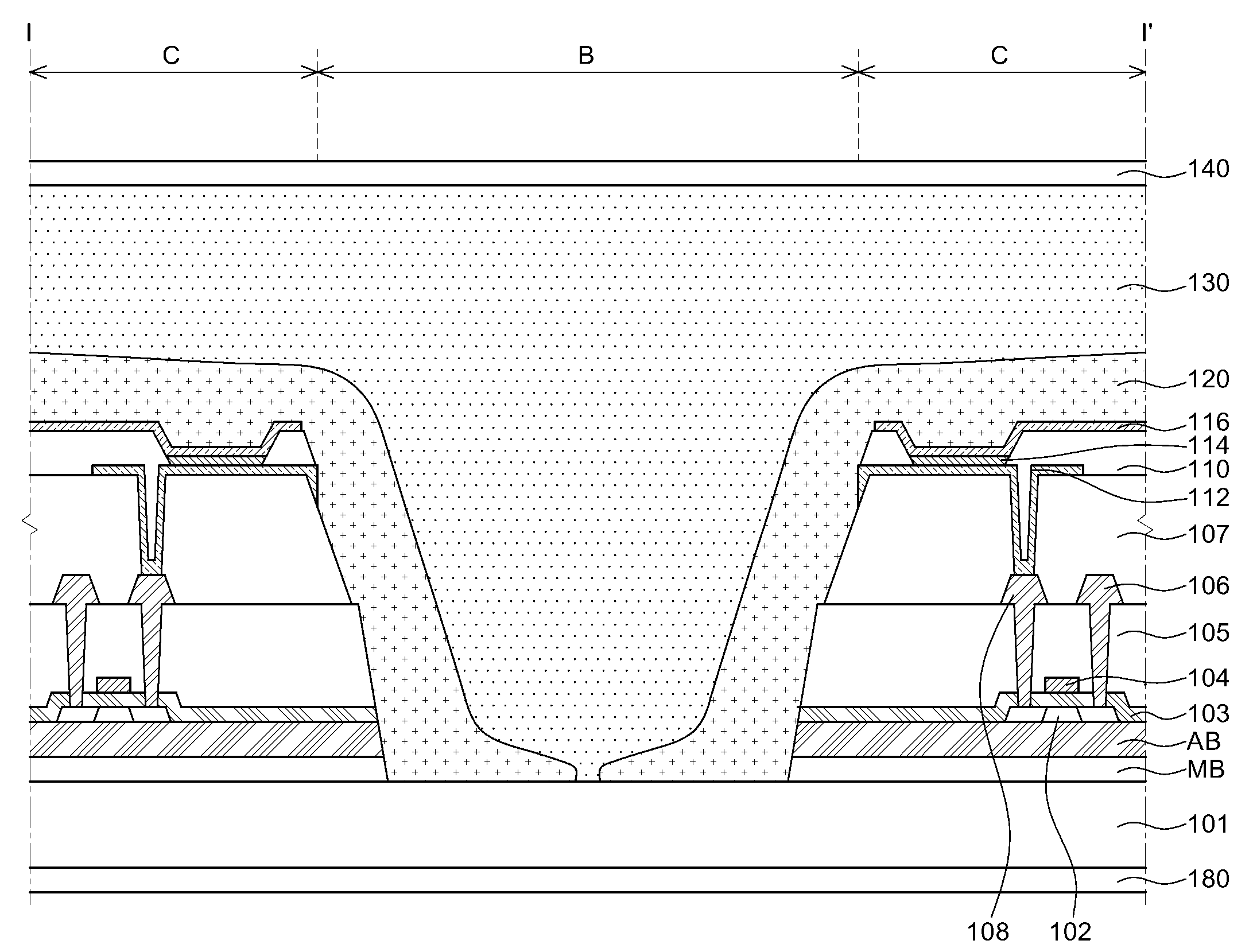
도 3 및 도 4는 도 2c의 특정 부분을 나타낸 단면도이다.Figures 3 and 4 are cross-sectional views showing specific portions of Figure 2c.
도 3은 도 2c의 1-1' 선을 따른 단면도이다. 도시된 유기발광 표시장치(100)는 내구성 강화 구조를 포함하고 있다. Fig. 3 is a cross-sectional view taken along line 1-1' of Fig. 2c. The illustrated organic light-emitting display device (100) includes a durability-enhanced structure.
상기 유기발광 표시장치(100)는 베이스 층(101) 상에 박막트랜지스터(102, 104, 106, 108), 유기발광소자(112, 114, 116) 및 각종 기능 층(layer)이 위치하고 있다. The above organic light-emitting display device (100) has thin film transistors (102, 104, 106, 108), organic light-emitting elements (112, 114, 116) and various functional layers positioned on a base layer (101).
상기 베이스 층(101)은 유기발광 표시장치(100)의 다양한 구성요소들을 지지한다. 베이스 층(101)은 투명한 절연 물질, 예를 들어 유리, 플라스틱 등과 같은 절연 물질로 형성될 수 있다. 기판(어레이 기판)은, 그 위에 형성된 소자 및 기능 층, 예를 들어 스위칭 TFT, 스위칭 TFT와 연결된 구동 TFT, 구동 TFT와 연결된 유기발광소자, 보호막 등을 포함하는 개념으로 지칭되기도 한다.The above base layer (101) supports various components of the organic light-emitting display device (100). The base layer (101) may be formed of a transparent insulating material, for example, an insulating material such as glass or plastic. The substrate (array substrate) is also referred to as a concept including elements and functional layers formed thereon, for example, a switching TFT, a driving TFT connected to the switching TFT, an organic light-emitting element connected to the driving TFT, a protective film, etc.
버퍼 층(buffer layer)이 베이스 층(101) 상에 위치할 수 있다. 상기 버퍼 층(MB, AB)은 베이스 층(101) 또는 하부의 층들에서 유출되는 알칼리 이온 등과 같은 불순물로부터 박막트랜지스터(Thin Film Transistor: TFT)를 보호하기 위한 기능 층이다. 상기 버퍼 층은 실리콘 산화물(SiOx), 실리콘 질화물(SiNx) 또는 이들의 다층으로 이루어질 수 있다. A buffer layer may be positioned on the base layer (101). The buffer layer (MB, AB) is a functional layer for protecting a thin film transistor (TFT) from impurities such as alkali ions leaking from the base layer (101) or lower layers. The buffer layer may be formed of silicon oxide (SiOx), silicon nitride (SiNx), or a multilayer thereof.
상기 베이스 층(101) 또는 버퍼 층 위에 박막트랜지스터가 놓인다. 박막트랜지스터는 반도체 층(102), 게이트 절연막(103), 게이트 전극(104), 층간 절연막(105), 소스 및 드레인 전극(106, 108)이 순차적으로 배치된 형태일 수 있다. 반도체 층(102)은 상기 베이스 층(101) 또는 버퍼 층 상에 위치한다. 반도체 층(102)은 폴리 실리콘(p-Si)으로 만들어질 수 있으며, 이 경우 소정의 영역이 불순물로 도핑될 수도 있다. 또한, 반도체 층(102)은 아몰포스 실리콘(a-Si)으로 만들어질 수도 있고, 펜타센 등과 같은 다양한 유기 반도체 물질로 만들어질 수도 있다. 나아가 반도체 층(102)은 산화물(oxide)로 만들어질 수도 있다. 게이트 절연막(103)은 실리콘 산화물(SiOx) 또는 실리콘 질화물(SiNx) 등과 같은 절연성 무기물로 형성될 수 있으며, 이외에도 절연성 유기물 등으로 형성될 수도 있다. 게이트 전극(104)은 다양한 도전성 물질, 예컨대, 마그네슘(Mg), 알루미늄(Al), 니켈(Ni), 크롬(Cr), 몰리브덴(Mo), 텅스텐(W), 금(Au) 또는 이들의 합금 등으로 형성될 수 있다.A thin film transistor is placed on the base layer (101) or buffer layer. The thin film transistor may have a form in which a semiconductor layer (102), a gate insulating film (103), a gate electrode (104), an interlayer insulating film (105), and source and drain electrodes (106, 108) are sequentially arranged. The semiconductor layer (102) is positioned on the base layer (101) or buffer layer. The semiconductor layer (102) may be made of polysilicon (p-Si), in which case a predetermined region may be doped with an impurity. In addition, the semiconductor layer (102) may be made of amorphous silicon (a-Si) or may be made of various organic semiconductor materials such as pentacene. Furthermore, the semiconductor layer (102) may be made of an oxide. The gate insulating film (103) may be formed of an insulating inorganic material such as silicon oxide (SiOx) or silicon nitride (SiNx), and may also be formed of an insulating organic material. The gate electrode (104) may be formed of various conductive materials such as magnesium (Mg), aluminum (Al), nickel (Ni), chromium (Cr), molybdenum (Mo), tungsten (W), gold (Au), or alloys thereof.
층간 절연막(105)은 실리콘 산화물(SiOx) 또는 실리콘 질화물(SiNx) 등과 같은 절연성 물질로 형성될 수 있으며, 이외에도 절연성 유기물 등으로 형성될 수도 있다. 층간 절연막(105)과 게이트 절연막(103)의 선택적 제거로 소스 및 드레인 영역이 노출되는 컨택 홀(contact hole)이 형성될 수 있다.The interlayer insulating film (105) may be formed of an insulating material such as silicon oxide (SiOx) or silicon nitride (SiNx), and may also be formed of an insulating organic material. By selectively removing the interlayer insulating film (105) and the gate insulating film (103), a contact hole exposing the source and drain regions may be formed.
소스 및 드레인 전극(106, 108)은 층간 절연막(105) 상에 전극용 물질로 단일층 또는 다층의 형상으로 형성된다.The source and drain electrodes (106, 108) are formed in a single layer or multilayer shape using electrode materials on an interlayer insulating film (105).
평탄화 층(107)이 박막트랜지스터 상에 위치할 수 있다. 평탄화 층(107)은 박막트랜지스터를 보호하고 그 상부를 평탄화한다. 평탄화 층(107)은 다양한 형태로 구성될 수 있는데, BCB(Benzocyclobutene) 또는 아크릴(Acryl) 등과 같은 유기 절연막, 또는 실리콘 질화막(SiNx), 실리콘 산화막(SiOx)와 같은 무기 절연막으로 형성될 수도 있고, 단층으로 형성되거나 이중 혹은 다중 층으로 구성될 수도 있는 등 다양한 변형이 가능하다.A planarization layer (107) may be positioned on the thin film transistor. The planarization layer (107) protects the thin film transistor and planarizes its upper portion. The planarization layer (107) may be configured in various forms, and may be formed of an organic insulating film such as BCB (Benzocyclobutene) or Acryl, or an inorganic insulating film such as a silicon nitride film (SiNx) or a silicon oxide film (SiOx), and may be formed in a single layer or configured in a double or multi-layer, and various modifications are possible.
유기발광소자는 제1 전극(112), 유기발광 층(114), 제2 전극(116)이 순차적으로 배치된 형태일 수 있다. 즉, 유기발광소자는 평탄화 층(107) 상에 형성된 제1 전극(112), 제1 전극(112) 상에 위치한 유기발광 층(114) 및 유기발광 층(114) 상에 위치한 제2 전극(116)으로 구성될 수 있다.The organic light-emitting device may be in a form in which a first electrode (112), an organic light-emitting layer (114), and a second electrode (116) are sequentially arranged. That is, the organic light-emitting device may be composed of a first electrode (112) formed on a planarization layer (107), an organic light-emitting layer (114) positioned on the first electrode (112), and a second electrode (116) positioned on the organic light-emitting layer (114).
제1 전극(112)은 컨택 홀을 통해 구동 박막트랜지스터의 드레인 전극(108)과 전기적으로 연결된다. 유기발광 표시장치(100)가 상부 발광(top emission) 방식인 경우, 이러한 제1 전극(112)은 반사율이 높은 불투명한 도전 물질로 만들어질 수 있다. 예를 들면, 제1 전극(112)은 은(Ag), 알루미늄(Al), 금(Au), 몰리브덴(Mo), 텅스텐(W), 크롬(Cr) 또는 이들의 합금 등으로 형성될 수 있다.The first electrode (112) is electrically connected to the drain electrode (108) of the driving thin film transistor through a contact hole. If the organic light-emitting display device (100) is of a top emission type, the first electrode (112) may be made of an opaque conductive material having high reflectivity. For example, the first electrode (112) may be formed of silver (Ag), aluminum (Al), gold (Au), molybdenum (Mo), tungsten (W), chromium (Cr), or an alloy thereof.
뱅크(110)는 발광 영역을 제외한 나머지 영역에 형성된다. 이에 따라, 뱅크(110)는 발광 영역과 대응되는 제1 전극(112)을 노출시키는 뱅크 홀을 가진다. 뱅크(110)는 실리콘 질화막(SiNx), 실리콘 산화막(SiOx)와 같은 무기 절연 물질 또는 BCB, 아크릴계 수지 또는 이미드계 수지와 같은 유기 절연물질로 만들어질 수 있다.The bank (110) is formed in the remaining area except for the light-emitting area. Accordingly, the bank (110) has a bank hole that exposes the first electrode (112) corresponding to the light-emitting area. The bank (110) can be made of an inorganic insulating material such as a silicon nitride film (SiNx) or a silicon oxide film (SiOx), or an organic insulating material such as BCB, an acrylic resin, or an imide resin.
유기발광 층(114)이 뱅크(110)에 의해 노출된 제1 전극(112) 상에 위치한다. 유기발광 층(114)은 발광층, 전자주입층, 전자수송층, 정공수송층, 정공주입층 등을 포함할 수 있다. 상기 유기발광 층은, 하나의 빛을 발광하는 단일 발광층 구조로 구성될 수도 있고, 복수 개의 발광층으로 구성되어 백색 광을 발광하는 구조로 구성될 수도 있다. An organic light-emitting layer (114) is positioned on the first electrode (112) exposed by the bank (110). The organic light-emitting layer (114) may include a light-emitting layer, an electron injection layer, an electron transport layer, a hole transport layer, a hole injection layer, etc. The organic light-emitting layer may be configured as a single light-emitting layer structure that emits one light, or may be configured as a structure that emits white light by being configured as a plurality of light-emitting layers.
제2 전극(116)이 유기발광층(114) 상에 위치한다. 유기발광 표시장치(100)가 상부 발광(top emission) 방식인 경우, 제2 전극(116)은 인듐 틴 옥사이드(Indium Tin Oxide; ITO) 또는 인듐 징크 옥사이드(Induim Zinc Oxide; IZO) 등과 같은 투명한 도전 물질로 형성됨으로써 유기발광 층(114)에서 생성된 광을 제2 전극(116) 상부로 방출시킨다.The second electrode (116) is positioned on the organic light-emitting layer (114). When the organic light-emitting display device (100) is of the top emission type, the second electrode (116) is formed of a transparent conductive material such as indium tin oxide (ITO) or indium zinc oxide (IZO), thereby emitting light generated in the organic light-emitting layer (114) to the upper portion of the second electrode (116).
봉지 층(120)이 제2 전극(116) 상에 위치한다. 상기 봉지 층(120)은, 발광 재료와 전극 재료의 산화를 방지하기 위하여, 외부로부터의 산소 및 수분 침투를 막는다. 유기발광소자가 수분이나 산소에 노출되면, 발광 영역이 축소되는 화소 수축(pixel shrinkage) 현상이 나타나거나, 발광 영역 내 흑점(dark spot)이 생길 수 있다. 상기 보호 층(passivation layer) 및/또는 상기 봉지 층(encapsulation layer)은 유리, 금속, 산화 알루미늄(AlOx) 또는 실리콘(Si) 계열 물질로 이루어진 무기막으로 구성되거나, 또는 유기막과 무기막이 교대로 적층된 구조일 수도 있다. 무기막은 수분이나 산소의 침투를 차단하는 역할을 하고, 유기막은 무기막의 표면을 평탄화하는 역할을 한다. 봉지 층을 여러 겹의 박막 층으로 형성하는 이유는, 단일 층에 비해 수분이나 산소의 이동 경로를 길고 복잡하게 하여, 유기발광소자까지 수분/산소의 침투를 어렵게 만들려는 것이다. 상기 봉지 층(120)은 제 1 영역에서 끊어질 수 있다. 상기 봉지 층(120)은 수분 침투를 막기 위한 무기막을 포함하기 때문에, 굴곡 부분인 제1 영역(B)에는 상기 봉지 층(120)이 최소로 존재하는 것이 바람직하다. 따라서, 상기 봉지 층은 상기 제1 영역(B)의 적어도 일부를 덮지 않는다.A passivation layer (120) is positioned on the second electrode (116). The passivation layer (120) prevents the oxidation of the light-emitting material and the electrode material, thereby preventing the penetration of oxygen and moisture from the outside. When the organic light-emitting element is exposed to moisture or oxygen, a pixel shrinkage phenomenon in which the light-emitting area is reduced may occur, or dark spots may occur within the light-emitting area. The passivation layer and/or the encapsulation layer may be composed of an inorganic film made of glass, metal, aluminum oxide (AlOx), or silicon (Si) series materials, or may have a structure in which organic films and inorganic films are alternately laminated. The inorganic film serves to block the penetration of moisture or oxygen, and the organic film serves to flatten the surface of the inorganic film. The reason for forming the encapsulation layer as multiple thin film layers is to make the movement path of moisture or oxygen longer and more complicated compared to a single layer, thereby making it difficult for moisture/oxygen to penetrate to the organic light-emitting element. The above-described encapsulating layer (120) can be broken in the first region. Since the encapsulating layer (120) includes an inorganic film to prevent moisture penetration, it is preferable that the encapsulating layer (120) is present at a minimum in the first region (B), which is a bent portion. Accordingly, the encapsulating layer does not cover at least a portion of the first region (B).
사용자의 터치 입력을 감지하기 위한 터치 층이 상기 봉지 층(120) 상면에 마련될 수 있다. 필요하다면, 터치 감지 전극 및/또는 터치 입력 감지와 연관된 다른 부품이 구비된 독립된 층이 상기 표시장치(100) 내부에 마련될 수 있다. 상기 터치 감지 전극(예: 터치 구동/감지 전극)은 인듐 주석 산화물, 그래핀(graphene)과 같은 탄소 기반 물질, 탄소 나노튜브, 전도성 고분자, 다양한 전도성/비전도성 물질의 혼합물로 만들어진 하이브리드 물질 등의 투명 전도성 물질로 형성될 수 있다. 또한, 금속 메쉬(metal mesh), 예컨대, 알루미늄 메쉬, 은 메쉬 등이 상기 터치 감지 전극으로 사용될 수 있다.A touch layer for detecting a user's touch input may be provided on an upper surface of the encapsulation layer (120). If necessary, an independent layer equipped with a touch detection electrode and/or other components related to touch input detection may be provided inside the display device (100). The touch detection electrode (e.g., touch drive/detection electrode) may be formed of a transparent conductive material, such as indium tin oxide, a carbon-based material such as graphene, carbon nanotubes, a conductive polymer, a hybrid material made of a mixture of various conductive/non-conductive materials, etc. In addition, a metal mesh, such as an aluminum mesh, a silver mesh, etc., may be used as the touch detection electrode.
커버 층(140)이 상기 봉지 층(120) 상에 마련될 수 있다. 상기 커버층(140)은 상기 표시장치(100)를 보호하기 위해 사용될 수 있으며 일 예로 커버 글래스(cover glass)일 수 있다. 한편, 표시 특성(예: 외부 광 반사, 색 정확도, 휘도 등)을 제어하기 위해 편광 층이 상기 커버 층(140)에 일체화될 수도 있다. (예: coated-pol) A cover layer (140) may be provided on the sealing layer (120). The cover layer (140) may be used to protect the display device (100) and may be, for example, a cover glass. Meanwhile, a polarizing layer may be integrated into the cover layer (140) to control display characteristics (e.g., external light reflection, color accuracy, brightness, etc.). (e.g., coated-pol)
상기 폴더블 표시장치(100)의 특정 부분에서의 강도 및/또는 견고성을 증가시키기 위해, 하나 이상의 지지 층(180)이 상기 베이스 층(101)의 하부에 제공될 수 있다. 상기 지지 층(180)은, 상기 베이스 층(101)의 양면 중 유기발광소자가 있는 면(제1 면)의 반대편 면(제2 면)에 부착된다. 상기 지지 층(180)은 폴리에틸렌 나프탈레이트(Polyethylene Naphthalate; PEN), 폴리에틸렌 테레프탈레이트(Ployethylene Terephthalate; PET), 폴리에틸렌 에테르프탈레이트 (polyethylene ether phthalate), 폴리카보네이트(polycarbonate), 폴리아릴레이트(polyarylate), 폴리에테르이미드(polyether imide), 폴리에테르술폰산(polyether sulfonate), 폴리이미드(polyimide) 폴리아크릴레이트(polyacrylate), 기타 적합한 폴리머의 조합으로 구성된 박형 플라스틱 필름으로 만들어질 수 있다. 상기 지지 층(180)의 형성에 사용될 수 있는 다른 적합한 물질은 박형 유리, 유전체로 차폐된 금속 호일(metal foil), 다층 폴리머, 나노 파티클 또는 마이크로 파티클과 조합된 고분자 물질이 포함된 고분자 필름 등일 수 있다. 상기 봉지층(120)와 커버 층(140) 사이, 그리고, 상기 베이스 층(101)과 지지 층(180) 사이에는 접착 층이 놓일 수 있다. 상기 접착 층은 열 경화형 또는 자연 경화형의 접착제일 수 있다. 예를 들어, 상기 접착 층은 OCA, B-PSA(Barrier pressure sensitive adhesive)와 같은 물질로 구성될 수 있다.In order to increase strength and/or rigidity in a specific portion of the foldable display device (100), one or more support layers (180) may be provided under the base layer (101). The support layers (180) are attached to a side (second side) of the base layer (101) opposite to a side (first side) having an organic light-emitting element among both surfaces of the base layer (101). The support layers (180) may be made of a thin plastic film composed of a combination of polyethylene naphthalate (PEN), polyethylene terephthalate (PET), polyethylene ether phthalate, polycarbonate, polyarylate, polyether imide, polyether sulfonate, polyimide, polyacrylate, and other suitable polymers. Other suitable materials that can be used to form the support layer (180) may be thin glass, a metal foil shielded with a dielectric, a multilayer polymer, a polymer film containing a polymer material combined with nano-particles or micro-particles, etc. An adhesive layer may be placed between the sealing layer (120) and the cover layer (140), and between the base layer (101) and the support layer (180). The adhesive layer may be a heat-curable or natural-curable adhesive. For example, the adhesive layer may be composed of a material such as OCA, B-PSA (Barrier pressure sensitive adhesive).
일 실시예로서, 상기 유기발광 표시장치(100)는, 소정의 축을 따라 접힐 수 있는 하나 이상의 제1 영역(B) 및 상기 제1 영역(B)에 인접한 제2 영역(C)을 구비한 베이스 층(101); 상기 베이스 층의 제2 영역(C)에 적층된 박막 트랜지스터, 유기발광 소자 및 기능 층들을 포함한다. 이때 상기 제1 영역(B)은, 상기 제2 영역(C)에 적층된 박막 트랜지스터, 유기발광 소자 및 기능 층들이 존재하지 않고, 그 대신 해당 공간을 채운 충진 층(130)을 포함한다. As an example, the organic light-emitting display device (100) includes a base layer (101) having at least one first region (B) that can be folded along a predetermined axis and a second region (C) adjacent to the first region (B); thin film transistors, organic light-emitting elements, and functional layers laminated on the second region (C) of the base layer; wherein the first region (B) does not have the thin film transistors, organic light-emitting elements, and functional layers laminated on the second region (C), and instead includes a filling layer (130) that fills the corresponding space.
상기 제1 영역(B)은, 상기 제2 영역(C)의 박막 트랜지스터 및 유기발광 소자와 연관된 기능 층들이 식각된 영역일 수 있다. 즉, 상기 제1 영역(B)은, 더 잘 굽혀질 수 있도록 그 두께가 최소화된 영역이며, 크랙 발생/전파의 원인이 되는 물질들을 미리 제거한 영역이다. 또한 상기 제1 영역(B)은, 상기 제거된 층(물질)들이 있었던 공간이 탄성 물질로 채워져서, 패터닝으로 인한 강성 약화가 보완된 영역이기도 하다.The first region (B) may be a region where functional layers associated with the thin film transistor and the organic light-emitting element of the second region (C) are etched. That is, the first region (B) is a region whose thickness is minimized so that it can be bent better, and is a region where materials that cause crack occurrence/propagation are removed in advance. In addition, the first region (B) is a region where the space where the removed layers (materials) were is filled with an elastic material, thereby compensating for the weakening of rigidity due to patterning.
상기 제2 영역(C)은 표시 영역 및 그 양 측단의 비표시 영역까지 포함할 수 있다. 일 예로, 상기 제2 영역(C)은 그 양 측단 중 적어도 일 단에 제어 회로(예: GIP) 블록을 포함할 수 있다. 상기 봉지 층(120)은 도 3과 같이 상기 제2 영역(C)에서 단절될 수 있다 즉, 상기 봉지 층(120)은 상기 제2 영역의 전부 또는 일부를 덮지 않도록 구비될 수 있다.The second region (C) may include a display region and non-display regions at both ends thereof. For example, the second region (C) may include a control circuit (e.g., GIP) block at at least one of the two end portions thereof. The sealing layer (120) may be disconnected from the second region (C) as shown in FIG. 3. That is, the sealing layer (120) may be provided so as not to cover all or part of the second region.
상기 충진 층(130)은 상기 제1 영역(B)에 가해지는 응력을 견디기에 충분한 탄성력을 가진 물질로서, 폴리이미드 등의 고분자 화합물(polymer), 레진(resin) 등일 수 있다. 이때 상기 충진 층(130)은 2 내지 15 MPa의 탄성 계수(elastic modulus)를 가질 수 있다. The above filling layer (130) is a material having sufficient elasticity to withstand the stress applied to the first region (B), and may be a polymer compound such as polyimide, resin, etc. In this case, the filling layer (130) may have an elastic modulus of 2 to 15 MPa.
또한 상기 충진 층(130)은 액체, 졸(so;) 또는 젤(gel) 상태의 물질일 수도 있다. 이 경우에, 상기 충진 층(130)은 화학적으로 안정적인 불활성 물질로 이뤄질 수 있다. 예를 들어, 상기 충진 층(130)은 폴리디메틸실록산(Polydimethylsiloxane: PDMS), 액체 흡착제(getter) 등의 물질로 구성될 수 있다. 상기 PDMS로 이루어진 충진 층(130)은 약 13~14 MPa 탄성율 및 50~1000 cps의 점도(viscosity)를 가질 수 있다. 한편 상기 충진 층(130)은 광 투과율이 90% 이상이 되도록 구비되어 시인성 저하를 최소화할 수 있다. 더 나아가 상기 충진 층(130)은 액정을 포함하여 편광판(polarizer)의 역할도 함께 수행할 수 있다. 이 경우에 표시장치의 전체 두께를 더 얇게 할 수 있어 폴더블/롤러블 특성이 향상된다.In addition, the filling layer (130) may be a material in a liquid, sol, or gel state. In this case, the filling layer (130) may be made of a chemically stable inert material. For example, the filling layer (130) may be made of a material such as polydimethylsiloxane (PDMS), a liquid getter, etc. The filling layer (130) made of PDMS may have an elastic modulus of about 13 to 14 MPa and a viscosity of 50 to 1000 cps. Meanwhile, the filling layer (130) may be provided so that the light transmittance is 90% or higher to minimize the reduction in visibility. Furthermore, the filling layer (130) may also function as a polarizer by including a liquid crystal. In this case, the overall thickness of the display device may be made thinner, thereby improving the foldable/rollable characteristics.
상기 충진 층(130)은 액체, 졸(so;) 또는 젤(gel)인 경우에, 도 5a 및 5b에 도시된 보조 구조물(190)이 더 구비될 수 있다. 상기 보조 구조물(190)은 표시장치가 접히거나 말릴 때 충진 층의 형태(높이, 분포도 등)을 일정하게 유지하기 위해 마련된다. 즉, 상기 보조 구조물(190)은 뱅크가 오픈된 개구 영역(EA)을 제외한 부분에 위치하여 충진 층의 지나친 유동을 제어한다. 상기 보조 구조물(190)은 뱅크(110)의 상부에 저온 포토 아크릴(PAC) 등의 재료로 형성될 수 있다.When the above-described filling layer (130) is a liquid, sol, or gel, the auxiliary structure (190) illustrated in FIGS. 5a and 5b may be further provided. The auxiliary structure (190) is provided to maintain the shape (height, distribution, etc.) of the filling layer constant when the display device is folded or rolled. That is, the auxiliary structure (190) is positioned in a portion excluding the opening area (EA) where the bank is open to control excessive flow of the filling layer. The auxiliary structure (190) may be formed of a material such as low-temperature photoacrylic (PAC) on the upper portion of the bank (110).
한편, 상기 충진 층(130)은, 도 3과 같이, 상기 제1 영역(B)뿐만 아니라 상기 제2 영역(C)의 상부도 덮을 수 있다. Meanwhile, the filling layer (130) can cover not only the first region (B) but also the upper part of the second region (C), as shown in FIG. 3.
도 4는 도 2c의 2-2' 선을 따른 단면도이다. 도 4에는 박막 트랜지스터가 도시되지 않았으나, 특정 실시 예에 따라서는 해당 부분에 박막 트랜지스터가 위치할 수도 있다. 도 4에 도시된 각종 기능 층들은 도 3에서 설명한 것과 동일하다.Fig. 4 is a cross-sectional view taken along line 2-2' of Fig. 2c. Although a thin film transistor is not illustrated in Fig. 4, a thin film transistor may be positioned in that portion depending on a specific embodiment. The various functional layers illustrated in Fig. 4 are the same as those described in Fig. 3.
도 4에 도시된 부분은 제1 영역(B)을 사이에 두고 제2 영역(C)에 배치된 픽셀(R, G, B) 사이를 연결하는 전기적 도선(108)을 포함하고 있다. 상기 도선(108)은 표시장치의 구부러짐 또는 접힘 시에 가해지는 응력(stress)을 저감시키는 형태를 가질 수 있다. 예를 들어, 상기 도선은 도 2c에 도시된 다이아몬드 형상 외에도 물결 형상, 삼각파 형상, 사각파 형상 등 응력 분산에 적합한 형상으로 구현될 수 있다.The part illustrated in FIG. 4 includes an electrical conductor (108) that connects pixels (R, G, B) arranged in a second region (C) with a first region (B) in between. The conductor (108) may have a shape that reduces stress applied when the display device is bent or folded. For example, the conductor may be implemented in a shape suitable for stress distribution, such as a wave shape, a triangular wave shape, a square wave shape, in addition to the diamond shape illustrated in FIG. 2c.
상기 도선(108)은 박막 트랜지스터의 소스 또는 드레인 전극과 동일한 물질로 만들어질 수 있다. 이때 상기 도선(108)은 상기 소스 또는 드레인 전극의 형성 공정에서 동시에 만들어질 수 있다.The above conductor (108) may be made of the same material as the source or drain electrode of the thin film transistor. In this case, the conductor (108) may be made simultaneously in the formation process of the source or drain electrode.
상기 표시장치(100)는 접힘 영역에 형성된 내구성 향상 구조를 포함함으로써, 접힘 신뢰성이 더욱 향상될 수 있다. The above display device (100) can further improve folding reliability by including a durability-enhancing structure formed in the folding area.
이상 첨부된 도면을 참조하여 본 명세서의 실시예들을 상세하게 설명하였으나, 본 명세서는 반드시 이러한 실시예로 국한되는 것은 아니고, 그 기술사상을 벗어나지 않는 범위 내에서 다양하게 변형 실시될 수 있다. 따라서, 본 명세서에 개시된 실시예들은 본 발명의 기술 사상을 한정하기 위한 것이 아니라 설명하기 위한 것이고, 이러한 실시예에 의하여 본 발명의 기술 사상의 범위가 한정되는 것은 아니다. 본 발명의 여러 실시예들의 각각 특징들이 부분적으로 또는 전체적으로 서로 결합 또는 조합 가능하고, 당업자에 의해 기술적으로 다양하게 연동 및 구동될 수 있으며, 각 실시예들이 서로에 대하여 독립적으로 실시되거나 연관 관계로 함께 실시될 수도 있다. 본 발명의 보호 범위는 아래의 청구범위에 의하여 해석되어야 하며, 그와 동등한 범위 내에 있는 모든 기술 사상은 본 발명의 권리범위에 포함되는 것으로 해석되어야 할 것이다.Although the embodiments of the present specification have been described in detail with reference to the attached drawings, the present specification is not necessarily limited to these embodiments, and various modifications may be made without departing from the technical idea thereof. Accordingly, the embodiments disclosed in this specification are not intended to limit the technical idea of the present invention but to explain it, and the scope of the technical idea of the present invention is not limited by these embodiments. The respective features of the various embodiments of the present invention may be partially or wholly combined or combined with each other, and may be technically linked and operated in various ways by those skilled in the art, and the respective embodiments may be implemented independently of each other or implemented together in a related relationship. The protection scope of the present invention should be interpreted by the following claims, and all technical ideas within a scope equivalent thereto should be interpreted as being included in the scope of the rights of the present invention.
Claims (17)
상기 베이스 층의 제2 영역에 적층된 박막 트랜지스터, 유기발광 소자 및 복수의 절연 층; 및
상기 제1 영역과 상기 제2 영역에 적층된 봉지 층을 포함하고,
상기 제1 영역은, 상기 제2 영역에 적층된 박막 트랜지스터, 유기발광 소자 및 복수의 절연 층이 존재하지 않고, 그 대신 해당 공간을 채운 충진 층을 포함하며,
상기 봉지 층은 상기 제2 영역에서 상기 유기발광 소자의 상부에 배치되어 상기 베이스 층과 접하도록 상기 제1 영역으로 연장되되, 상기 제1 영역의 전체 영역 중 일부에 존재하지 않고, 그 대신 상기 충진 층에 의해 채워지는 것을 특징으로 하는 표시 장치.A base layer having at least one first region foldable along a predetermined axis and a second region adjacent to the first region;
A thin film transistor, an organic light-emitting element and a plurality of insulating layers laminated in a second region of the base layer; and
Including a bag layer laminated on the first region and the second region,
The first region does not have a thin film transistor, an organic light-emitting element, and a plurality of insulating layers stacked on the second region, and instead includes a filling layer filling the space.
A display device characterized in that the encapsulating layer is disposed on top of the organic light-emitting element in the second region and extends to the first region so as to be in contact with the base layer, but does not exist in a portion of the entire area of the first region, but instead is filled by the filling layer.
상기 충진 층은 폴리이미드를 포함하는 표시장치.In the first paragraph,
A display device wherein the above filling layer comprises polyimide.
상기 충진 층은 2 내지 15 MPa의 탄성 계수를 갖는 물질인 표시장치.In the second paragraph,
A display device wherein the above filling layer is a material having an elastic modulus of 2 to 15 MPa.
상기 충진 층은 상기 제2 영역의 상부에도 있는 표시장치.In the first paragraph,
The above filling layer is a display device also located on the upper part of the second region.
상기 제1 영역은, 상기 제2 영역의 박막 트랜지스터, 유기발광 소자 및 복수의 절연 층이 식각된 영역인, 표시장치.In the first paragraph,
A display device, wherein the first region is a region in which a thin film transistor, an organic light-emitting element, and a plurality of insulating layers of the second region are etched.
상기 제2 영역은 표시 영역 및 그 양 측단의 비표시 영역까지 포함하는 표시장치.In the first paragraph,
The above second region is a display device including a display region and a non-display region on both sides thereof.
상기 제2 영역은 그 양 측단의 제어 회로 블록을 포함한 표시장치.In Article 6,
The above second region is a display device including control circuit blocks on both sides thereof.
상기 제1 영역은, 상기 제1 영역을 사이에 두고 이격된 제2 영역들에 있는 픽셀 사이를 연결하는 도선을 포함한 표시장치.In the first paragraph,
A display device including a first region and a second region that are spaced apart from the first region.
상기 도선은, 다이아몬드, 물결 형상, 사각파 형상 또는 톱니파 형상을 갖는 표시장치.In Article 8,
The above conductor is a display device having a diamond, wave shape, square wave shape or sawtooth wave shape.
상기 제1 영역은 서로 다른 두 방향으로 연장된 표시장치.In the first paragraph,
The above first region is a display device extending in two different directions.
상기 충진 층은 액체 졸(sol) 또는 젤(gel) 상태의 물질인 표시장치.In the first paragraph,
A display device in which the above-mentioned filling layer is a material in a liquid sol or gel state.
상기 충진 층은 폴리디메틸실록산(Polydimethylsiloxane)으로 구성된 표시장치.In Article 11,
The above filling layer is a display device composed of polydimethylsiloxane.
상기 충진 층은, 13 내지 14 MPa의 탄성율 및 50 내지 1000 cps의 점도를 갖는 표시장치.In Article 12,
The above-mentioned filling layer is a display device having an elastic modulus of 13 to 14 MPa and a viscosity of 50 to 1000 cps.
상기 충진 층은 액정을 더 포함하는 표시장치.In Article 11,
A display device wherein the above filling layer further includes a liquid crystal.
상기 충진 층 위에 배치된 커버 층을 더 포함하며,
상기 제2 영역의 복수의 절연 층의 최상 층은 뱅크이고,
상기 뱅크의 상부의 상기 커버 층과 상기 충진 층 사이에는 상기 커버 층과 접하는 보조 구조물이 구비된 표시장치.In Article 11,
Further comprising a cover layer disposed on the above filling layer,
The uppermost layer of the plurality of insulating layers of the second region is a bank,
A display device having an auxiliary structure in contact with the cover layer between the cover layer and the filling layer on the upper part of the bank.
상기 베이스 층의 제2 영역에 적층된 박막 트랜지스터, 유기발광 소자 및 복수의 절연 층을 포함하고,
상기 제1 영역은, 상기 제2 영역에 적층된 박막 트랜지스터, 유기발광 소자 및 복수의 절연 층이 존재하지 않고, 그 대신 해당 공간을 채운 충진 층을 포함하며,
상기 제1 영역은 서로 다른 2 방향의 접힘 축과 나란한 메쉬 패턴으로 배열되며,
상기 충진 층은 액체 졸(sol) 또는 젤(gel) 상태의 물질인, 표시 장치.A base layer having at least one first region foldable along a predetermined axis and a second region adjacent to the first region;
It comprises a thin film transistor, an organic light-emitting element and a plurality of insulating layers laminated in the second region of the base layer,
The first region does not have a thin film transistor, an organic light-emitting element, and a plurality of insulating layers stacked on the second region, and instead includes a filling layer filling the space.
The above first region is arranged in a mesh pattern parallel to the folding axes in two different directions,
A display device wherein the above-mentioned filling layer is a material in a liquid sol or gel state.
상기 베이스 층의 제2 영역에 적층된 박막 트랜지스터, 유기발광 소자 및 복수의 절연 층; 및
상기 제1 영역과 상기 제2 영역에 적층된 봉지 층을 포함하고,
상기 제1 영역은, 상기 제2 영역에 적층된 박막 트랜지스터, 유기발광 소자 및 복수의 절연 층이 존재하지 않고, 그 대신 해당 공간을 채운 충진 층을 포함하며,
상기 충진 층 위에 배치된 커버 층을 더 포함하며,
상기 제2 영역의 복수의 절연 층의 최상 층은 뱅크이고,
상기 뱅크의 상부의 상기 커버 층과 상기 봉지 층 사이에는 상기 커버 층과 접하는 보조 구조물이 구비되며,
상기 충진 층은 액체 졸(sol) 또는 젤(gel) 상태의 물질인, 표시 장치.A base layer having at least one first region foldable along a predetermined axis and a second region adjacent to the first region;
A thin film transistor, an organic light-emitting element and a plurality of insulating layers laminated in a second region of the base layer; and
Including a bag layer laminated on the first region and the second region,
The first region does not have a thin film transistor, an organic light-emitting element, and a plurality of insulating layers stacked on the second region, and instead includes a filling layer filling the space.
Further comprising a cover layer disposed on the above filling layer,
The uppermost layer of the plurality of insulating layers of the second region is a bank,
Between the cover layer and the bag layer on the upper part of the bank, an auxiliary structure in contact with the cover layer is provided.
A display device wherein the above-mentioned filling layer is a material in a liquid sol or gel state.
Priority Applications (3)
| Application Number | Priority Date | Filing Date | Title |
|---|---|---|---|
| US16/598,970 US11075347B2 (en) | 2018-10-22 | 2019-10-10 | Flexible display device |
| JP2019190125A JP6867461B2 (en) | 2018-10-22 | 2019-10-17 | Display device |
| EP19204584.7A EP3644370B1 (en) | 2018-10-22 | 2019-10-22 | Flexible display device |
Applications Claiming Priority (2)
| Application Number | Priority Date | Filing Date | Title |
|---|---|---|---|
| KR20180126003 | 2018-10-22 | ||
| KR1020180126003 | 2018-10-22 |
Publications (2)
| Publication Number | Publication Date |
|---|---|
| KR20200045382A KR20200045382A (en) | 2020-05-04 |
| KR102746370B1 true KR102746370B1 (en) | 2024-12-24 |
Family
ID=70732654
Family Applications (1)
| Application Number | Title | Priority Date | Filing Date |
|---|---|---|---|
| KR1020180156316A Active KR102746370B1 (en) | 2018-10-22 | 2018-12-06 | Flexible display device |
Country Status (1)
| Country | Link |
|---|---|
| KR (1) | KR102746370B1 (en) |
Families Citing this family (1)
| Publication number | Priority date | Publication date | Assignee | Title |
|---|---|---|---|---|
| KR102791770B1 (en) * | 2019-06-05 | 2025-04-08 | 삼성디스플레이 주식회사 | Display device |
Citations (2)
| Publication number | Priority date | Publication date | Assignee | Title |
|---|---|---|---|---|
| JP2015069861A (en) * | 2013-09-30 | 2015-04-13 | 株式会社ジャパンディスプレイ | Electroluminescent device and manufacturing method of the same |
| WO2018110529A1 (en) * | 2016-12-16 | 2018-06-21 | Dic株式会社 | Sealing material composition for display element, and display element in which said composition is used |
Family Cites Families (4)
| Publication number | Priority date | Publication date | Assignee | Title |
|---|---|---|---|---|
| KR102293835B1 (en) * | 2014-09-30 | 2021-08-25 | 엘지디스플레이 주식회사 | Organic light emitting diode display device |
| US9780157B2 (en) * | 2014-12-23 | 2017-10-03 | Lg Display Co., Ltd. | Flexible display device with gate-in-panel circuit |
| KR102399572B1 (en) * | 2015-09-15 | 2022-05-19 | 삼성디스플레이 주식회사 | Flexible display device |
| KR102639568B1 (en) * | 2016-03-11 | 2024-02-26 | 삼성디스플레이 주식회사 | Display apparatus and method of manufacturing the same |
-
2018
- 2018-12-06 KR KR1020180156316A patent/KR102746370B1/en active Active
Patent Citations (2)
| Publication number | Priority date | Publication date | Assignee | Title |
|---|---|---|---|---|
| JP2015069861A (en) * | 2013-09-30 | 2015-04-13 | 株式会社ジャパンディスプレイ | Electroluminescent device and manufacturing method of the same |
| WO2018110529A1 (en) * | 2016-12-16 | 2018-06-21 | Dic株式会社 | Sealing material composition for display element, and display element in which said composition is used |
Also Published As
| Publication number | Publication date |
|---|---|
| KR20200045382A (en) | 2020-05-04 |
Similar Documents
| Publication | Publication Date | Title |
|---|---|---|
| KR102633501B1 (en) | Foldable display device | |
| KR102762224B1 (en) | Organic light emitting display device | |
| KR20250050835A (en) | Organic light emitting display device | |
| US11075347B2 (en) | Flexible display device | |
| CN113126806A (en) | Touch display device | |
| KR102673973B1 (en) | Display Device | |
| KR102569727B1 (en) | Display device | |
| KR102664769B1 (en) | Display device | |
| KR20200052167A (en) | Foldable display device | |
| US11150753B2 (en) | Display device including a touch detecting unit having an insulating pattern | |
| KR20200058059A (en) | Organic light emitting display device | |
| KR20250166067A (en) | Flexible display device | |
| KR102811098B1 (en) | Display device | |
| KR102892291B1 (en) | Electroluminescent display device | |
| KR102746370B1 (en) | Flexible display device | |
| KR102561547B1 (en) | Electroluminescence display device | |
| CN114582933A (en) | Display device | |
| US12360627B2 (en) | Display device having discharge patterns in a pad area to discharge static electricity introduced into a driver | |
| KR102610485B1 (en) | Electroluminescent display device | |
| KR102637116B1 (en) | Organic light emitting display device | |
| KR20190017405A (en) | Flexible display device | |
| KR20220043560A (en) | Flexible display device |
Legal Events
| Date | Code | Title | Description |
|---|---|---|---|
| PA0109 | Patent application |
St.27 status event code: A-0-1-A10-A12-nap-PA0109 |
|
| PG1501 | Laying open of application |
St.27 status event code: A-1-1-Q10-Q12-nap-PG1501 |
|
| A201 | Request for examination | ||
| PA0201 | Request for examination |
St.27 status event code: A-1-2-D10-D11-exm-PA0201 |
|
| P22-X000 | Classification modified |
St.27 status event code: A-2-2-P10-P22-nap-X000 |
|
| P22-X000 | Classification modified |
St.27 status event code: A-2-2-P10-P22-nap-X000 |
|
| E902 | Notification of reason for refusal | ||
| PE0902 | Notice of grounds for rejection |
St.27 status event code: A-1-2-D10-D21-exm-PE0902 |
|
| T11-X000 | Administrative time limit extension requested |
St.27 status event code: U-3-3-T10-T11-oth-X000 |
|
| AMND | Amendment | ||
| P11-X000 | Amendment of application requested |
St.27 status event code: A-2-2-P10-P11-nap-X000 |
|
| P13-X000 | Application amended |
St.27 status event code: A-2-2-P10-P13-nap-X000 |
|
| E601 | Decision to refuse application | ||
| PE0601 | Decision on rejection of patent |
St.27 status event code: N-2-6-B10-B15-exm-PE0601 |
|
| X091 | Application refused [patent] | ||
| P11-X000 | Amendment of application requested |
St.27 status event code: A-2-2-P10-P11-nap-X000 |
|
| P13-X000 | Application amended |
St.27 status event code: A-2-2-P10-P13-nap-X000 |
|
| PX0901 | Re-examination |
St.27 status event code: A-2-3-E10-E12-rex-PX0901 |
|
| E90F | Notification of reason for final refusal | ||
| PE0902 | Notice of grounds for rejection |
St.27 status event code: A-1-2-D10-D21-exm-PE0902 |
|
| P11-X000 | Amendment of application requested |
St.27 status event code: A-2-2-P10-P11-nap-X000 |
|
| P13-X000 | Application amended |
St.27 status event code: A-2-2-P10-P13-nap-X000 |
|
| PX0701 | Decision of registration after re-examination |
St.27 status event code: A-3-4-F10-F13-rex-PX0701 |
|
| X701 | Decision to grant (after re-examination) | ||
| GRNT | Written decision to grant | ||
| PR0701 | Registration of establishment |
St.27 status event code: A-2-4-F10-F11-exm-PR0701 |
|
| PR1002 | Payment of registration fee |
St.27 status event code: A-2-2-U10-U11-oth-PR1002 Fee payment year number: 1 |
|
| PG1601 | Publication of registration |
St.27 status event code: A-4-4-Q10-Q13-nap-PG1601 |
|
| P22-X000 | Classification modified |
St.27 status event code: A-4-4-P10-P22-nap-X000 |