KR102722916B1 - Integrated circuit device and method of manufacturing the same - Google Patents
Integrated circuit device and method of manufacturing the same Download PDFInfo
- Publication number
- KR102722916B1 KR102722916B1 KR1020190058311A KR20190058311A KR102722916B1 KR 102722916 B1 KR102722916 B1 KR 102722916B1 KR 1020190058311 A KR1020190058311 A KR 1020190058311A KR 20190058311 A KR20190058311 A KR 20190058311A KR 102722916 B1 KR102722916 B1 KR 102722916B1
- Authority
- KR
- South Korea
- Prior art keywords
- memory stack
- substrate
- peripheral
- word lines
- wiring layer
- Prior art date
- Legal status (The legal status is an assumption and is not a legal conclusion. Google has not performed a legal analysis and makes no representation as to the accuracy of the status listed.)
- Active
Links
Images


Classifications
-
- H—ELECTRICITY
- H10—SEMICONDUCTOR DEVICES; ELECTRIC SOLID-STATE DEVICES NOT OTHERWISE PROVIDED FOR
- H10B—ELECTRONIC MEMORY DEVICES
- H10B41/00—Electrically erasable-and-programmable ROM [EEPROM] devices comprising floating gates
-
- H—ELECTRICITY
- H01—ELECTRIC ELEMENTS
- H01L—SEMICONDUCTOR DEVICES NOT COVERED BY CLASS H10
- H01L21/00—Processes or apparatus adapted for the manufacture or treatment of semiconductor or solid state devices or of parts thereof
- H01L21/70—Manufacture or treatment of devices consisting of a plurality of solid state components formed in or on a common substrate or of parts thereof; Manufacture of integrated circuit devices or of parts thereof
- H01L21/71—Manufacture of specific parts of devices defined in group H01L21/70
- H01L21/768—Applying interconnections to be used for carrying current between separate components within a device comprising conductors and dielectrics
- H01L21/76838—Applying interconnections to be used for carrying current between separate components within a device comprising conductors and dielectrics characterised by the formation and the after-treatment of the conductors
-
- H—ELECTRICITY
- H01—ELECTRIC ELEMENTS
- H01L—SEMICONDUCTOR DEVICES NOT COVERED BY CLASS H10
- H01L21/00—Processes or apparatus adapted for the manufacture or treatment of semiconductor or solid state devices or of parts thereof
- H01L21/70—Manufacture or treatment of devices consisting of a plurality of solid state components formed in or on a common substrate or of parts thereof; Manufacture of integrated circuit devices or of parts thereof
- H01L21/71—Manufacture of specific parts of devices defined in group H01L21/70
- H01L21/768—Applying interconnections to be used for carrying current between separate components within a device comprising conductors and dielectrics
- H01L21/76897—Formation of self-aligned vias or contact plugs, i.e. involving a lithographically uncritical step
-
- H—ELECTRICITY
- H10—SEMICONDUCTOR DEVICES; ELECTRIC SOLID-STATE DEVICES NOT OTHERWISE PROVIDED FOR
- H10B—ELECTRONIC MEMORY DEVICES
- H10B41/00—Electrically erasable-and-programmable ROM [EEPROM] devices comprising floating gates
- H10B41/10—Electrically erasable-and-programmable ROM [EEPROM] devices comprising floating gates characterised by the top-view layout
-
- H—ELECTRICITY
- H10—SEMICONDUCTOR DEVICES; ELECTRIC SOLID-STATE DEVICES NOT OTHERWISE PROVIDED FOR
- H10B—ELECTRONIC MEMORY DEVICES
- H10B41/00—Electrically erasable-and-programmable ROM [EEPROM] devices comprising floating gates
- H10B41/20—Electrically erasable-and-programmable ROM [EEPROM] devices comprising floating gates characterised by three-dimensional arrangements, e.g. with cells on different height levels
- H10B41/23—Electrically erasable-and-programmable ROM [EEPROM] devices comprising floating gates characterised by three-dimensional arrangements, e.g. with cells on different height levels with source and drain on different levels, e.g. with sloping channels
- H10B41/27—Electrically erasable-and-programmable ROM [EEPROM] devices comprising floating gates characterised by three-dimensional arrangements, e.g. with cells on different height levels with source and drain on different levels, e.g. with sloping channels the channels comprising vertical portions, e.g. U-shaped channels
-
- H—ELECTRICITY
- H10—SEMICONDUCTOR DEVICES; ELECTRIC SOLID-STATE DEVICES NOT OTHERWISE PROVIDED FOR
- H10B—ELECTRONIC MEMORY DEVICES
- H10B41/00—Electrically erasable-and-programmable ROM [EEPROM] devices comprising floating gates
- H10B41/30—Electrically erasable-and-programmable ROM [EEPROM] devices comprising floating gates characterised by the memory core region
-
- H—ELECTRICITY
- H10—SEMICONDUCTOR DEVICES; ELECTRIC SOLID-STATE DEVICES NOT OTHERWISE PROVIDED FOR
- H10B—ELECTRONIC MEMORY DEVICES
- H10B41/00—Electrically erasable-and-programmable ROM [EEPROM] devices comprising floating gates
- H10B41/40—Electrically erasable-and-programmable ROM [EEPROM] devices comprising floating gates characterised by the peripheral circuit region
-
- H—ELECTRICITY
- H10—SEMICONDUCTOR DEVICES; ELECTRIC SOLID-STATE DEVICES NOT OTHERWISE PROVIDED FOR
- H10B—ELECTRONIC MEMORY DEVICES
- H10B41/00—Electrically erasable-and-programmable ROM [EEPROM] devices comprising floating gates
- H10B41/50—Electrically erasable-and-programmable ROM [EEPROM] devices comprising floating gates characterised by the boundary region between the core region and the peripheral circuit region
-
- H—ELECTRICITY
- H10—SEMICONDUCTOR DEVICES; ELECTRIC SOLID-STATE DEVICES NOT OTHERWISE PROVIDED FOR
- H10B—ELECTRONIC MEMORY DEVICES
- H10B43/00—EEPROM devices comprising charge-trapping gate insulators
-
- H—ELECTRICITY
- H10—SEMICONDUCTOR DEVICES; ELECTRIC SOLID-STATE DEVICES NOT OTHERWISE PROVIDED FOR
- H10B—ELECTRONIC MEMORY DEVICES
- H10B43/00—EEPROM devices comprising charge-trapping gate insulators
- H10B43/10—EEPROM devices comprising charge-trapping gate insulators characterised by the top-view layout
-
- H—ELECTRICITY
- H10—SEMICONDUCTOR DEVICES; ELECTRIC SOLID-STATE DEVICES NOT OTHERWISE PROVIDED FOR
- H10B—ELECTRONIC MEMORY DEVICES
- H10B43/00—EEPROM devices comprising charge-trapping gate insulators
- H10B43/20—EEPROM devices comprising charge-trapping gate insulators characterised by three-dimensional arrangements, e.g. with cells on different height levels
- H10B43/23—EEPROM devices comprising charge-trapping gate insulators characterised by three-dimensional arrangements, e.g. with cells on different height levels with source and drain on different levels, e.g. with sloping channels
- H10B43/27—EEPROM devices comprising charge-trapping gate insulators characterised by three-dimensional arrangements, e.g. with cells on different height levels with source and drain on different levels, e.g. with sloping channels the channels comprising vertical portions, e.g. U-shaped channels
-
- H—ELECTRICITY
- H10—SEMICONDUCTOR DEVICES; ELECTRIC SOLID-STATE DEVICES NOT OTHERWISE PROVIDED FOR
- H10B—ELECTRONIC MEMORY DEVICES
- H10B43/00—EEPROM devices comprising charge-trapping gate insulators
- H10B43/30—EEPROM devices comprising charge-trapping gate insulators characterised by the memory core region
-
- H—ELECTRICITY
- H10—SEMICONDUCTOR DEVICES; ELECTRIC SOLID-STATE DEVICES NOT OTHERWISE PROVIDED FOR
- H10B—ELECTRONIC MEMORY DEVICES
- H10B43/00—EEPROM devices comprising charge-trapping gate insulators
- H10B43/40—EEPROM devices comprising charge-trapping gate insulators characterised by the peripheral circuit region
-
- H—ELECTRICITY
- H10—SEMICONDUCTOR DEVICES; ELECTRIC SOLID-STATE DEVICES NOT OTHERWISE PROVIDED FOR
- H10B—ELECTRONIC MEMORY DEVICES
- H10B43/00—EEPROM devices comprising charge-trapping gate insulators
- H10B43/50—EEPROM devices comprising charge-trapping gate insulators characterised by the boundary region between the core and peripheral circuit regions
-
- H10W20/031—
-
- H10W20/069—
-
- H10W20/2134—
-
- H10W20/42—
-
- H10W20/43—
-
- H10W72/073—
-
- H10W90/00—
-
- H10W20/20—
-
- H10W72/823—
-
- H10W90/22—
-
- H10W90/297—
-
- H10W90/734—
Landscapes
- Engineering & Computer Science (AREA)
- Microelectronics & Electronic Packaging (AREA)
- Power Engineering (AREA)
- Computer Hardware Design (AREA)
- Physics & Mathematics (AREA)
- Condensed Matter Physics & Semiconductors (AREA)
- General Physics & Mathematics (AREA)
- Semiconductor Memories (AREA)
- Geometry (AREA)
- Non-Volatile Memory (AREA)
- Manufacturing & Machinery (AREA)
- Internal Circuitry In Semiconductor Integrated Circuit Devices (AREA)
Abstract
집적회로 소자는 기판 상에 배치된 복수의 하부 워드 라인을 포함하는 하부 메모리 스택과, 상기 하부 메모리 스택 상에 배치되고 복수의 상부 워드 라인을 포함하는 상부 메모리 스택과, 상기 하부 메모리 스택과 상기 상부 메모리 스택과의 사이의 제1 수직 레벨을 따라 상기 수평 방향으로 연장되고, 상기 복수의 하부 워드 라인 중에서 선택되는 적어도 하나에 전기적으로 연결 가능하도록 구성된 적어도 하나의 제1 하부 배선층과, 상기 적어도 하나의 제1 하부 배선층을 덮는 분리 절연막과, 상기 상부 메모리 스택보다 높은 제2 수직 레벨을 따라 상기 수평 방향으로 연장되고 상기 복수의 상부 워드 라인 중에서 선택되는 적어도 하나에 전기적으로 연결 가능하도록 구성된 적어도 하나의 제1 상부 배선층을 포함한다. An integrated circuit device includes a lower memory stack disposed on a substrate, the lower memory stack including a plurality of lower word lines, an upper memory stack disposed on the lower memory stack and including a plurality of upper word lines, at least one first lower wiring layer extending in the horizontal direction along a first vertical level between the lower memory stack and the upper memory stack and configured to be electrically connectable to at least one selected from the plurality of lower word lines, an isolation insulating film covering the at least one first lower wiring layer, and at least one first upper wiring layer extending in the horizontal direction along a second vertical level higher than the upper memory stack and configured to be electrically connectable to at least one selected from the plurality of upper word lines.
Description
본 발명의 기술적 사상은 집적회로 소자 및 그 제조 방법에 관한 것으로, 특히 불휘발성 수직형 메모리 소자를 구비한 집적회로 소자 및 그 제조 방법에 관한 것이다. The technical idea of the present invention relates to an integrated circuit device and a method for manufacturing the same, and more particularly, to an integrated circuit device having a nonvolatile vertical memory device and a method for manufacturing the same.
정보 통신 장치의 다기능화에 따라 메모리 소자를 포함하는 집적회로 소자의 대용량화 및 고집적화가 요구되고 있다. 고집적화를 위한 메모리 셀 크기의 축소에 따라, 메모리 소자의 동작 및 전기적 연결을 위해 메모리 소자에 포함되는 동작 회로들 및 배선 구조들도 복잡해지고 있다. 이에 따라, 집적도를 향상시키면서 전기적 특성이 우수한 구조의 메모리 소자를 포함하는 집적회로 소자가 요구되고 있다.As information and communication devices become more multifunctional, integrated circuit devices including memory elements are required to have larger capacities and higher integration. As the memory cell size is reduced for higher integration, the operating circuits and wiring structures included in the memory elements for the operation and electrical connection of the memory elements are also becoming more complex. Accordingly, integrated circuit elements including memory elements with excellent electrical characteristics while improving integration are required.
본 발명의 기술적 사상이 이루고자 하는 기술적 과제는 수직형 메모리 소자에서 집적도 향상을 위하여 워드 라인의 적층 수가 증가되고, 워드 라인에 연결되는 콘택의 수 및 배선의 수가 증가되어도 메모리 소자의 점유 면적을 감소시켜 칩 면적을 감소시킬 수 있고 배선 배치 자유도를 향상시킬 수 있으며, 워드 라인의 적층 수가 증가되어도 콘택 형성을 위한 공정 난이도가 높아지지 않고 단순화된 공정으로 제조할 수 있는 집적회로 소자 및 그 제조 방법을 제공하는 것이다. The technical problem to be achieved by the technical idea of the present invention is to provide an integrated circuit device and a method for manufacturing the same, which can reduce the chip area by reducing the area occupied by the memory device and improve the freedom of wiring arrangement even when the number of stacked word lines increases for improving the integration level in a vertical memory device and the number of contacts and the number of wiring connected to the word lines are increased, and can be manufactured with a simplified process without increasing the difficulty of the process for forming contacts even when the number of stacked word lines increases.
본 발명의 기술적 사상에 의한 일 양태에 따른 집적회로 소자는 메모리 셀 영역 및 연결 영역을 포함하는 기판과, 상기 기판의 메모리 셀 영역 및 연결 영역 상에서 상기 기판의 주면에 평행한 수평 방향으로 연장되고 수직 방향에서 서로 오버랩되어 있는 복수의 하부 워드 라인을 포함하는 하부 메모리 스택과, 상기 하부 메모리 스택 상에 배치되고 상기 수직 방향에서 서로 오버랩되어 있는 복수의 상부 워드 라인을 포함하는 상부 메모리 스택과, 상기 연결 영역 상에서 상기 하부 메모리 스택과 상기 상부 메모리 스택과의 사이의 제1 수직 레벨을 따라 상기 수평 방향으로 연장되고, 상기 복수의 하부 워드 라인 중에서 선택되는 적어도 하나의 하부 워드 라인에 전기적으로 연결 가능하도록 구성된 적어도 하나의 제1 하부 배선층과, 상기 연결 영역 상에서 적어도 하나의 제1 하부 배선층의 상면이 다른 도전체와 접하지 않도록 상기 적어도 하나의 제1 하부 배선층을 덮는 분리 절연막과, 상기 연결 영역 상에서 상기 상부 메모리 스택보다 높은 제2 수직 레벨을 따라 상기 수평 방향으로 연장되고, 상기 복수의 상부 워드 라인 중에서 선택되는 적어도 하나의 상부 워드 라인에 전기적으로 연결 가능하도록 구성된 적어도 하나의 제1 상부 배선층을 포함한다. According to one aspect of the technical idea of the present invention, an integrated circuit device comprises: a substrate including a memory cell region and a connection region; a lower memory stack including a plurality of lower word lines extending in a horizontal direction parallel to a main surface of the substrate on the memory cell region and the connection region of the substrate and overlapping each other in a vertical direction; an upper memory stack including a plurality of upper word lines arranged on the lower memory stack and overlapping each other in the vertical direction; at least one first lower wiring layer extending in the horizontal direction along a first vertical level between the lower memory stack and the upper memory stack on the connection region and configured to be electrically connectable to at least one lower word line selected from the plurality of lower word lines; an isolation insulating film covering the at least one first lower wiring layer so that an upper surface of the at least one first lower wiring layer does not come into contact with another conductor on the connection region; and at least one first upper wiring layer extending in the horizontal direction along a second vertical level higher than the upper memory stack on the connection region and configured to be electrically connectable to at least one upper word line selected from the plurality of upper word lines. Includes.
본 발명의 기술적 사상에 의한 다른 양태에 따른 집적회로 소자는 메모리 셀 영역 및 연결 영역을 포함하는 기판과, 상기 메모리 셀 영역으로부터 이격되고 복수의 회로를 포함하는 주변회로 영역과, 상기 메모리 셀 영역 상에서 상기 기판의 주면에 평행한 수평 방향으로 연장되고 수직 방향에서 상호 오버랩되어 있는 복수의 하부 워드 라인과, 상기 복수의 하부 워드 라인에 연결되고 상기 연결 영역 상에서 계단형 하부 연결부를 구성하는 복수의 하부 패드 영역을 포함하는 하부 메모리 스택과, 상기 메모리 셀 영역 상에서 상기 하부 메모리 스택 위에 배치되고, 상기 수평 방향으로 연장되고 상기 수직 방향에서 상호 오버랩되어 있는 복수의 상부 워드 라인과, 상기 복수의 상부 워드 라인에 연결되고 상기 연결 영역 상에서 계단형 상부 연결부를 구성하는 복수의 상부 패드 영역을 포함하는 상부 메모리 스택과, 상기 연결 영역 상에서 상기 계단형 하부 연결부를 덮는 하부 절연막과, 상기 복수의 하부 패드 영역으로부터 상기 하부 절연막을 관통하여 상기 상부 메모리 스택보다 낮은 제1 수직 레벨까지 연장된 복수의 하부 콘택 플러그와, 상기 하부 메모리 스택과 상기 상부 메모리 스택과의 사이에 배치된 복수의 제1 하부 배선층을 포함하고, 상기 복수의 제1 하부 배선층 중 적어도 하나의 제1 하부 배선층은 상기 복수의 하부 콘택 플러그 중 적어도 하나에 연결되는 제1 국부와, 상기 복수의 회로 중 적어도 하나에 연결되는 제2 국부를 포함한다. According to another aspect of the technical idea of the present invention, an integrated circuit device comprises: a substrate including a memory cell region and a connection region; a peripheral circuit region spaced from the memory cell region and including a plurality of circuits; a lower memory stack including a plurality of lower word lines extending in a horizontal direction parallel to a main surface of the substrate on the memory cell region and overlapping each other in a vertical direction; and a plurality of lower pad regions connected to the plurality of lower word lines and forming a stepped lower connection portion on the connection region; an upper memory stack disposed above the lower memory stack on the memory cell region, including a plurality of upper word lines extending in the horizontal direction and overlapping each other in the vertical direction; and a plurality of upper pad regions connected to the plurality of upper word lines and forming a stepped upper connection portion on the connection region; a lower insulating film covering the stepped lower connection portion on the connection region; a plurality of lower contact plugs extending from the plurality of lower pad regions through the lower insulating film to a first vertical level lower than the upper memory stack; and a plurality of first lower wiring layers disposed between the lower memory stack and the upper memory stack. and wherein at least one first lower wiring layer of the plurality of first lower wiring layers comprises a first local portion connected to at least one of the plurality of lower contact plugs and a second local portion connected to at least one of the plurality of circuits.
본 발명의 기술적 사상에 의한 또 다른 양태에 따른 집적회로 소자는 메모리 셀 영역 및 연결 영역을 포함하는 제1 기판과, 상기 메모리 셀 영역 상에서 상기 제1 기판의 주면에 평행한 수평 방향으로 연장되고 수직 방향으로 서로 오버랩되어 있는 복수의 하부 워드 라인과, 상기 복수의 하부 워드 라인에 연결되고 상기 연결 영역 상에 배치된 복수의 하부 패드 영역을 포함하는 하부 메모리 스택과, 상기 메모리 셀 영역 상에서 상기 하부 메모리 스택 상에 배치되고 상기 수직 방향으로 서로 오버랩되어 있는 복수의 상부 워드 라인과, 상기 복수의 상부 워드 라인에 연결되고 상기 연결 영역 상에 배치된 복수의 상부 패드 영역을 포함하는 상부 메모리 스택과, 상기 연결 영역 상에서 상기 하부 메모리 스택과 상기 상부 메모리 스택과의 사이의 제1 수직 레벨을 따라 상기 수평 방향으로 연장된 적어도 하나의 제1 하부 배선층과, 상기 복수의 하부 패드 영역 중에서 선택되는 적어도 하나의 하부 패드 영역과 상기 적어도 하나의 제1 하부 배선층과의 사이에 연결된 적어도 하나의 하부 콘택 플러그와, 상기 연결 영역 상에서 상기 적어도 하나의 제1 하부 배선층의 상면이 다른 도전체와 접하지 않도록 상기 적어도 하나의 제1 하부 배선층을 덮는 분리 절연막을 포함한다. According to another aspect of the technical idea of the present invention, an integrated circuit device comprises: a first substrate including a memory cell region and a connection region; a lower memory stack including a plurality of lower word lines extending in a horizontal direction parallel to a main surface of the first substrate on the memory cell region and overlapping each other in a vertical direction; a plurality of lower pad regions connected to the lower word lines and arranged on the connection region; an upper memory stack including a plurality of upper word lines arranged on the lower memory stack on the memory cell region and overlapping each other in the vertical direction; and a plurality of upper pad regions connected to the plurality of upper word lines and arranged on the connection region; at least one first lower wiring layer extending in the horizontal direction along a first vertical level between the lower memory stack and the upper memory stack on the connection region; at least one lower contact plug connected between at least one lower pad region selected from the plurality of lower pad regions and the at least one first lower wiring layer; and a lower contact plug covering the at least one first lower wiring layer so that an upper surface of the at least one first lower wiring layer does not come into contact with another conductor on the connection region. Includes a separating insulating film.
본 발명의 기술적 사상에 의한 일 양태에 따른 집적회로 소자의 제조 방법에서는 기판을 준비한다. 상기 기판 상에서 상기 기판의 주면에 평행한 수평 방향으로 연장되고 수직 방향에서 서로 오버랩되어 있는 복수의 하부 워드 라인과, 상기 복수의 하부 워드 라인에 연결되는 복수의 하부 패드 영역을 포함하는 하부 메모리 스택을 형성한다. 상기 복수의 하부 패드 영역 중에서 선택되는 복수의 제1 하부 패드 영역에 연결되는 복수의 제1 하부 콘택 플러그를 포함하는 복수의 하부 콘택 플러그를 형성한다. 상기 기판 상에서 상기 하부 메모리 스택의 레벨보다 높은 제1 수직 레벨을 따라 상기 수평 방향으로 연장되고, 상기 복수의 제1 하부 콘택 플러그에 연결되는 복수의 제1 하부 배선층을 포함하는 복수의 하부 배선층을 형성한다. 상기 복수의 하부 배선층 위에서 상기 복수의 하부 배선층을 덮는 분리 절연막을 형성한다. 상기 분리 절연막을 사이에 두고 상기 하부 메모리 스택과 상기 수직 방향에서 이격되도록 배치되고, 상기 수직 방향에서 서로 오버랩되어 있는 복수의 상부 워드 라인과, 상기 복수의 상부 워드 라인에 연결되는 복수의 상부 패드 영역을 포함하는 상부 메모리 스택을 형성한다. 상기 복수의 상부 패드 영역에 연결되는 복수의 제1 상부 콘택 플러그를 포함하는 복수의 상부 콘택 플러그를 형성한다. 상기 제1 수직 레벨보다 높은 제2 수직 레벨을 따라 상기 수평 방향으로 연장되고, 상기 복수의 상부 콘택 플러그에 연결되는 복수의 상부 배선층을 형성한다. In one aspect of the technical idea of the present invention, a method for manufacturing an integrated circuit device is provided by preparing a substrate. On the substrate, a lower memory stack is formed, which includes a plurality of lower word lines extending in a horizontal direction parallel to a main surface of the substrate and overlapping each other in a vertical direction, and a plurality of lower pad regions connected to the plurality of lower word lines. A plurality of lower contact plugs are formed, which include a plurality of first lower contact plugs connected to a plurality of first lower pad regions selected from the plurality of lower pad regions. A plurality of lower wiring layers are formed, which include a plurality of first lower wiring layers extending in the horizontal direction along a first vertical level higher than a level of the lower memory stack on the substrate and connected to the plurality of first lower contact plugs. An isolation insulating film covering the plurality of lower wiring layers is formed over the plurality of lower wiring layers. An upper memory stack is formed, which includes a plurality of upper word lines arranged to be spaced apart from the lower memory stack in the vertical direction with the isolation insulating film interposed therebetween, and overlapping each other in the vertical direction, and a plurality of upper pad regions connected to the plurality of upper word lines. A plurality of upper contact plugs are formed, including a plurality of first upper contact plugs connected to the plurality of upper pad regions. A plurality of upper wiring layers are formed, extending in the horizontal direction along a second vertical level higher than the first vertical level, and connected to the plurality of upper contact plugs.
본 발명의 기술적 사상에 의한 다른 양태에 따른 집적회로 소자의 제조 방법에서는 기판 상에서 상기 기판의 주면에 평행한 수평 방향으로 연장되고 수직 방향에서 서로 오버랩되어 있는 복수의 하부 워드 라인과, 상기 복수의 하부 워드 라인에 연결되는 복수의 하부 패드 영역을 포함하는 하부 메모리 스택을 형성한다. 상기 기판 상에서 상기 복수의 하부 패드 영역에 연결되는 복수의 하부 콘택 플러그를 형성한다. 상기 기판 상에서 상기 하부 메모리 스택의 레벨보다 높은 제1 수직 레벨을 따라 상기 수평 방향으로 연장되고 상기 복수의 하부 콘택 플러그에 연결되는 복수의 하부 배선층을 형성한다. 상기 기판 상에서 상기 하부 메모리 스택 및 상기 복수의 하부 배선층을 덮는 분리 절연막을 형성한다. 본딩 기판 상에서 상기 수직 방향에서 서로 오버랩되어 있는 복수의 상부 워드 라인과, 상기 복수의 상부 워드 라인에 연결되는 복수의 상부 패드 영역을 포함하는 상부 메모리 스택을 형성한다. 상기 본딩 기판 상에서 상기 복수의 상부 패드 영역에 연결되는 복수의 상부 콘택 플러그를 형성한다. 상기 본딩 기판 상에서 상기 상부 메모리 스택의 레벨보다 높은 제2 수직 레벨을 따라 상기 수평 방향으로 연장되고 상기 복수의 상부 콘택 플러그에 연결되는 복수의 상부 배선층을 형성한다. 상기 하부 메모리 스택 및 상기 상부 메모리 스택이 상기 본딩 기판을 사이에 두고 서로 대면하도록 상기 분리 절연막과 상기 본딩 기판을 본딩한다. In another aspect of the technical idea of the present invention, a method for manufacturing an integrated circuit device comprises forming a lower memory stack on a substrate, the lower memory stack including a plurality of lower word lines extending in a horizontal direction parallel to a main surface of the substrate and overlapping each other in a vertical direction, and a plurality of lower pad regions connected to the lower word lines. A plurality of lower contact plugs connected to the lower pad regions are formed on the substrate. A plurality of lower wiring layers are formed on the substrate, the lower wiring layers extending in the horizontal direction along a first vertical level higher than a level of the lower memory stack and connected to the lower contact plugs. An isolation insulating film covering the lower memory stack and the lower wiring layers is formed on the substrate. An upper memory stack including a plurality of upper word lines overlapping each other in the vertical direction and a plurality of upper pad regions connected to the upper word lines is formed on a bonding substrate. A plurality of upper contact plugs connected to the upper pad regions are formed on the bonding substrate. A plurality of upper wiring layers are formed on the bonding substrate, which extend in the horizontal direction along a second vertical level higher than the level of the upper memory stack and are connected to the plurality of upper contact plugs. The isolation insulating film and the bonding substrate are bonded so that the lower memory stack and the upper memory stack face each other with the bonding substrate interposed therebetween.
본 발명의 기술적 사상에 의한 집적회로 소자에 의하면, 수직형 메모리 소자에서 집적도 향상을 위하여 워드 라인의 적층 수가 증가되고 워드 라인에 연결되는 콘택 플러그의 수 및 배선의 수가 증가되어도 메모리 소자의 점유 면적을 감소시켜 칩 면적을 감소시킬 수 있으며, 단순하고 효율적인 배선 배치가 가능하여 배선 배치 자유도를 향상시킬 수 있다. 또한, 상부 메모리 스택의 레벨보다 낮은 레벨의 영역을 하부 메모리 스택에 연결되는 배선 형성 공간으로 이용함으로써 수직 방향으로 서로 이격된 복수의 메모리 스택 각각의 계단형 연결부의 점유 면적을 줄일 수 있어 칩 사이즈를 줄이는 데 기여할 수 있다. According to the integrated circuit device according to the technical idea of the present invention, in order to improve the integration in a vertical memory device, the number of stacked word lines is increased and the number of contact plugs and the number of wiring connected to the word lines are increased, but the occupied area of the memory device is reduced to reduce the chip area, and simple and efficient wiring arrangement is possible, thereby improving the freedom of wiring arrangement. In addition, by utilizing an area at a level lower than that of the upper memory stack as a wiring formation space connected to the lower memory stack, the occupied area of each step-like connection of a plurality of memory stacks spaced apart from each other in the vertical direction can be reduced, which can contribute to reducing the chip size.
본 발명의 기술적 사상에 의한 집적회로 소자의 제조 방법에 의하면, 메모리 스택을 수직 방향을 따라 복수 개로 분할하여 형성하고, 분할된 복수의 메모리 스택에 연결되는 콘택 플러그 및 배선을 복수의 서로 다른 수직 레벨에 분할하여 형성하므로, 고도로 집적화된 수직형 메모리 소자 제조를 위하여 워드 라인의 적층 수가 증가되어도 콘택 홀 형성을 위한 식각 공정시 적절한 아스펙트 비(aspect ratio)를 유지할 수 있어 콘택 플러그 형성 및 배선 형성 공정을 단순화된 공정에 의해 효율적으로 수행할 수 있다. 또한, 워드 라인의 적층 수가 증가되어도 집적회로 소자의 제조 공정 중에 워드 라인들의 무너짐 현상에 따른 문제들을 방지할 수 있어 집적회로 소자의 제조 효율을 높이고 제조 단가를 낮출 수 있다. According to a method for manufacturing an integrated circuit device according to the technical idea of the present invention, a memory stack is formed by dividing the memory stack into a plurality of pieces along a vertical direction, and contact plugs and wirings connected to the plurality of divided memory stacks are formed by dividing them into a plurality of different vertical levels. Therefore, even if the number of word lines stacked increases for manufacturing a highly integrated vertical memory device, an appropriate aspect ratio can be maintained during an etching process for forming a contact hole, so that the contact plug formation and wiring formation processes can be efficiently performed by a simplified process. In addition, even if the number of word lines stacked increases, problems due to the collapse of word lines during the manufacturing process of the integrated circuit device can be prevented, so that the manufacturing efficiency of the integrated circuit device can be increased and the manufacturing cost can be reduced.
도 1은 본 발명의 기술적 사상에 의한 실시예들에 따른 집적회로 소자의 주요 구성 요소들을 보여주는 평면도이다.
도 2a는 도 1에 예시한 집적회로 소자의 A1 - A1' 선 단면 구성 및 A2 - A2' 선 단면 구성과, 상기 집적회로 소자의 주변회로 영역 중 일부 영역의 단면 구성을 보여주는 단면도이다. 도 2b는 도 1에 예시한 집적회로 소자의 B - B' 선 단면 구성을 보여주는 단면도이다.
도 3a 내지 도 3d는 각각 본 발명의 기술적 사상에 의한 실시예들에 따른 집적회로 소자에 포함되는 게이트 유전막의 다양한 구성을 설명하기 위한 단면도이다.
도 4는 도 1, 도 2a, 및 도 2b에 예시한 집적회로 소자의 예시적인 구성을 설명하기 위한 개략적인 블록 다이어그램이다.
도 5는 도 2a에 예시한 복수의 하부 배선층의 예시적인 평면 배치를 보여주는 평면도이다.
도 6은 도 2a에 예시한 복수의 상부 배선층의 예시적인 평면 배치를 보여주는 평면도이다.
도 7은 도 2a에 예시한 복수의 하부 주변 배선층의 예시적인 평면 배치를 보여주는 평면도이다.
도 8 내지 도 20은 각각 본 발명의 기술적 사상에 의한 다른 실시예들에 따른 집적회로 소자를 설명하기 위한 단면도이다.
도 21a 내지 도 21j는 본 발명의 기술적 사상에 의한 실시예들에 따른 집적회로 소자의 제조 방법을 설명하기 위하여 공정 순서에 따라 도시한 단면도들이다.
도 22a 및 도 22b는 본 발명의 기술적 사상에 의한 실시예들에 따른 집적회로 소자의 제조 방법을 설명하기 위하여 공정 순서에 따라 도시한 단면도들이다. FIG. 1 is a plan view showing major components of an integrated circuit device according to embodiments of the technical idea of the present invention.
FIG. 2a is a cross-sectional view showing the cross-sectional configuration of the integrated circuit element taken along line A1 - A1' and the cross-sectional configuration of the A2 - A2' of the integrated circuit element illustrated in FIG. 1, and the cross-sectional configuration of a part of a peripheral circuit area of the integrated circuit element. FIG. 2b is a cross-sectional view showing the cross-sectional configuration of the integrated circuit element taken along line B - B' of the integrated circuit element illustrated in FIG. 1.
FIGS. 3A to 3D are cross-sectional views each illustrating various configurations of a gate dielectric film included in an integrated circuit device according to embodiments of the technical idea of the present invention.
FIG. 4 is a schematic block diagram illustrating an exemplary configuration of the integrated circuit devices illustrated in FIGS. 1, 2a, and 2b.
FIG. 5 is a plan view showing an exemplary planar arrangement of a plurality of lower wiring layers as illustrated in FIG. 2a.
FIG. 6 is a plan view showing an exemplary planar arrangement of a plurality of upper wiring layers as illustrated in FIG. 2a.
FIG. 7 is a plan view showing an exemplary planar arrangement of a plurality of lower peripheral wiring layers illustrated in FIG. 2a.
FIGS. 8 to 20 are cross-sectional views each illustrating an integrated circuit device according to different embodiments of the technical idea of the present invention.
FIGS. 21A to 21J are cross-sectional views illustrating a manufacturing method of an integrated circuit device according to embodiments of the technical idea of the present invention in accordance with the process sequence.
FIGS. 22a and 22b are cross-sectional views illustrating a manufacturing method of an integrated circuit device according to embodiments of the technical idea of the present invention in accordance with the process sequence.
이하, 첨부 도면을 참조하여 본 발명의 실시예들을 상세히 설명한다. 도면상의 동일한 구성요소에 대해서는 동일한 참조부호를 사용하고, 이들에 대한 중복된 설명은 생략한다. Hereinafter, embodiments of the present invention will be described in detail with reference to the attached drawings. The same reference numerals are used for the same components in the drawings, and redundant descriptions thereof are omitted.
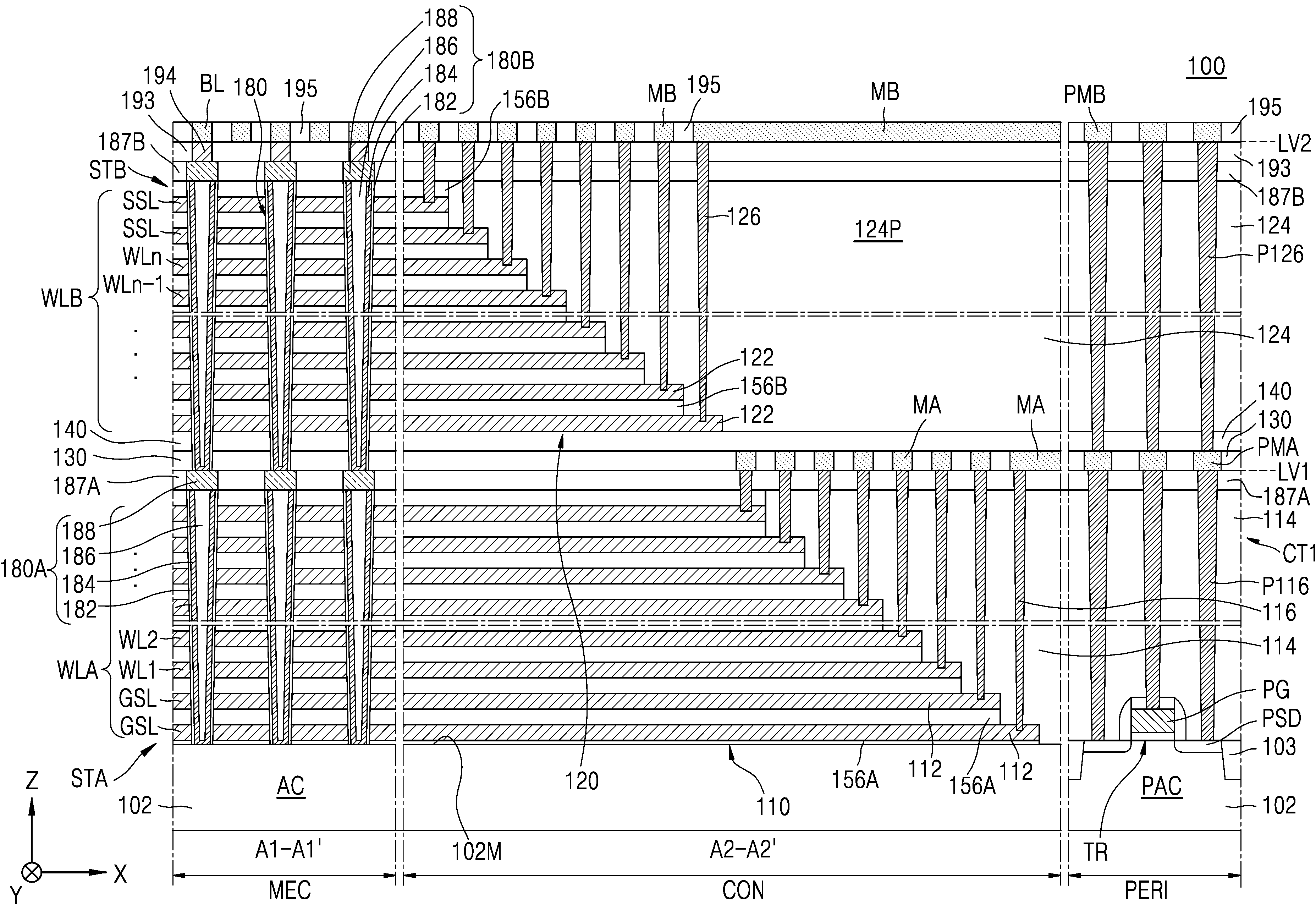
도 1은 본 발명의 기술적 사상에 의한 실시예들에 따른 집적회로 소자의 주요 구성 요소들을 보여주는 평면도이다. 도 2a는 도 1의 A1 - A1' 선 단면 구성 및 A2 - A2' 선 단면 구성과, 상기 집적회로 소자의 주변회로 영역(PERI) 중 일부 영역의 단면 구성을 보여주는 단면도이다. 도 2b는 도 1의 B - B' 선 단면 구성을 보여주는 단면도이다. FIG. 1 is a plan view showing major components of an integrated circuit device according to embodiments of the technical idea of the present invention. FIG. 2a is a cross-sectional view showing a cross-sectional configuration taken along line A1 - A1' and line A2 - A2' of FIG. 1, and a cross-sectional configuration of a portion of a peripheral circuit area (PERI) of the integrated circuit device. FIG. 2b is a cross-sectional view showing a cross-sectional configuration taken along line B - B' of FIG. 1.
도 1, 도 2a, 및 도 2b를 참조하면, 집적회로 소자(100)는 메모리 셀 영역(MEC), 연결 영역(CON), 및 주변회로 영역(PERI)을 가지는 기판(102)을 포함한다. 기판(102)은 X-Y 평면을 따르는 수평 방향으로 연장되는 주면(main surface)(102M)을 가질 수 있다. 기판(102)은 Si, Ge, 또는 SiGe를 포함할 수 있다. 메모리 셀 영역(MEC)의 활성 영역(AC) 상에 메모리 셀 어레이(MCA)가 형성될 수 있다. Referring to FIGS. 1, 2A, and 2B, an integrated circuit device (100) includes a substrate (102) having a memory cell region (MEC), a connection region (CON), and a peripheral circuit region (PERI). The substrate (102) may have a main surface (102M) extending in a horizontal direction along the X-Y plane. The substrate (102) may include Si, Ge, or SiGe. A memory cell array (MCA) may be formed on an active region (AC) of the memory cell region (MEC).
연결 영역(CON)은 메모리 셀 영역(MEC)의 에지측에 인접하게 배치될 수 있다. 메모리 셀 영역(MEC)은 연결 영역(CON)을 사이에 두고 주변회로 영역(PERI)과 이격될 수 있다. 도 1 및 도 2a에는 메모리 셀 영역(MEC)의 일측에 배치된 연결 영역(CON)만 도시되어 있으나, 메모리 셀 영역(MEC)의 제1 수평 방향(X 방향) 양측에 각각 연결 영역(CON)이 배치될 수 있다. The connection region (CON) may be arranged adjacent to the edge side of the memory cell region (MEC). The memory cell region (MEC) may be spaced apart from the peripheral circuit region (PERI) with the connection region (CON) therebetween. In FIGS. 1 and 2A, only the connection region (CON) arranged on one side of the memory cell region (MEC) is illustrated, but the connection region (CON) may be arranged on each of the first horizontal direction (X direction) sides of the memory cell region (MEC).
기판(102) 상에는 하부 메모리 스택(STA)이 배치되어 있다. 하부 메모리 스택(STA)은 복수의 하부 워드 라인(WLA)과, 복수의 하부 워드 라인(WLA)에 연결된 복수의 하부 패드 영역(112)을 포함한다. 복수의 하부 워드 라인(WLA)은 메모리 셀 영역(MEC) 상에 배치되고 기판(102)의 주면(102M)에 평행한 수평 방향으로 연장되고 수직 방향(Z 방향)에서 상호 오버랩되어 있다. 복수의 하부 패드 영역(112)은 연결 영역(CON) 상에 배치되고 계단형 하부 연결부(110)를 구성한다. A lower memory stack (STA) is arranged on a substrate (102). The lower memory stack (STA) includes a plurality of lower word lines (WLA) and a plurality of lower pad areas (112) connected to the plurality of lower word lines (WLA). The plurality of lower word lines (WLA) are arranged on a memory cell area (MEC) and extend in a horizontal direction parallel to a main surface (102M) of the substrate (102) and overlap each other in a vertical direction (Z direction). The plurality of lower pad areas (112) are arranged on a connection area (CON) and form a stepped lower connection portion (110).
하부 메모리 스택(STA) 상에는 상부 메모리 스택(STB)이 배치되어 있다. 상부 메모리 스택(STB)은 복수의 상부 워드 라인(WLB)과, 복수의 상부 워드 라인(WLB)에 연결된 복수의 상부 패드 영역(122)을 포함한다. 복수의 상부 워드 라인(WLB)은 메모리 셀 영역(MEC) 상에 배치되고 기판(102)의 주면(102M)에 평행한 수평 방향으로 연장되고 수직 방향(Z 방향)에서 상호 오버랩되어 있다. 복수의 상부 패드 영역(122)은 연결 영역(CON) 상에 배치되고 계단형 상부 연결부(120)를 구성한다. An upper memory stack (STB) is arranged on a lower memory stack (STA). The upper memory stack (STB) includes a plurality of upper word lines (WLB) and a plurality of upper pad areas (122) connected to the plurality of upper word lines (WLB). The plurality of upper word lines (WLB) are arranged on a memory cell area (MEC) and extend in a horizontal direction parallel to a main surface (102M) of a substrate (102) and overlap each other in a vertical direction (Z direction). The plurality of upper pad areas (122) are arranged on a connection area (CON) and form a stepped upper connection portion (120).
하부 메모리 스택(STA)은 48 개, 64 개, 또는 98 개의 하부 워드 라인(WLA)을 포함하고, 상부 메모리 스택(STB)은 48 개, 64 개, 또는 98 개의 상부 워드 라인(WLB)을 포함할 수 있으나, 상기 예시한 바에 한정되는 것은 아니다. 일부 실시예들에서, 복수의 하부 워드 라인(WLA)의 개수와 복수의 상부 워드 라인(WLB)의 개수의 합은 적어도 192 일 수 있다. The lower memory stack (STA) may include 48, 64, or 98 lower word lines (WLAs), and the upper memory stack (STB) may include 48, 64, or 98 upper word lines (WLBs), but is not limited to the above examples. In some embodiments, the sum of the number of the plurality of lower word lines (WLAs) and the number of the plurality of upper word lines (WLBs) may be at least 192.
복수의 하부 워드 라인(WLA) 및 복수의 상부 워드 라인(WLB)은 복수의 워드 라인(WL: WL1, WL2, …, WLn-1, WLn)과, 적어도 하나의 접지 선택 라인(GSL)과, 적어도 하나의 스트링 선택 라인(SSL)을 포함할 수 있다. 도 2a 및 도 2b에는 복수의 하부 워드 라인(WLA) 및 복수의 상부 워드 라인(WLB)에 2 개의 접지 선택 라인(GSL)과 2 개의 스트링 선택 라인(SSL)이 포함된 경우를 예시하였으나, 본 발명의 기술적 사상은 이에 한정되지 않는다. The plurality of lower word lines (WLA) and the plurality of upper word lines (WLB) may include a plurality of word lines (WL: WL1, WL2, ..., WLn-1, WLn), at least one ground select line (GSL), and at least one string select line (SSL). Although FIGS. 2A and 2B illustrate a case in which the plurality of lower word lines (WLA) and the plurality of upper word lines (WLB) include two ground select lines (GSL) and two string select lines (SSL), the technical idea of the present invention is not limited thereto.
수평 방향에서 하부 메모리 스택(STA)이 점유하는 면적은 상부 메모리 스택(STB)이 점유하는 면적보다 더 클 수 있다. 도 1 및 도 2a에 예시한 바와 같이, 수평 방향에서 계단형 하부 연결부(110)의 적어도 일부는 계단형 상부 연결부(120)보다 메모리 셀 영역(MEC)으로부터 더 멀어지는 방향으로 돌출될 수 있다. The area occupied by the lower memory stack (STA) in the horizontal direction may be larger than the area occupied by the upper memory stack (STB). As illustrated in FIGS. 1 and 2A, at least a portion of the stepped lower connector (110) in the horizontal direction may protrude further from the memory cell area (MEC) than the stepped upper connector (120).
복수의 워드 라인 컷 영역(WLC)이 기판(102)의 주면(102M)에 평행한 제1 수평 방향(X 방향)으로 연장될 수 있다. 복수의 워드 라인 컷 영역(WLC)은 제1 수평 방향(X 방향)에 수직인 제2 수평 방향(Y 방향)에서 복수의 하부 워드 라인(WLA) 및 복수의 상부 워드 라인(WLB) 각각의 폭을 한정할 수 있다. 복수의 하부 워드 라인(WLA) 및 복수의 상부 워드 라인(WLB)은 각각 복수의 워드 라인 컷 영역(WLC)에 의해 일정 간격으로 상호 이격되어 반복적으로 배치될 수 있다. A plurality of word line cut regions (WLC) can extend in a first horizontal direction (X direction) parallel to a main surface (102M) of a substrate (102). The plurality of word line cut regions (WLC) can define a width of each of the plurality of lower word lines (WLA) and the plurality of upper word lines (WLB) in a second horizontal direction (Y direction) perpendicular to the first horizontal direction (X direction). The plurality of lower word lines (WLA) and the plurality of upper word lines (WLB) can be repeatedly arranged to be spaced apart from each other at a predetermined interval by the plurality of word line cut regions (WLC), respectively.
기판(102)에는 복수의 공통 소스 영역(106)이 제1 수평 방향(X 방향)을 따라 연장될 수 있다. 일부 실시예들에서, 복수의 공통 소스 영역(106)은 n 형 불순물이 고농도로 도핑된 불순물 영역일 수 있다. 복수의 공통 소스 영역(106)은 수직형 메모리 셀들로 전류를 공급하는 소스 영역으로서 기능할 수 있다. 복수의 공통 소스 영역(106) 상에서 복수의 공통 소스 라인(CSL)이 제1 수평 방향(X 방향)을 따라 연장될 수 있다. 복수의 공통 소스 라인(CSL)은 복수의 하부 워드 라인(WLA) 및 복수의 상부 워드 라인(WLB) 각각의 일측에서 워드 라인 컷 영역(WLC)의 일부를 채우도록 형성될 수 있다. 복수의 공통 소스 라인(CSL)은 각각 하부 메모리 스택(STA)을 관통하는 하부 공통 소스 라인(CSLA)과, 상부 메모리 스택(STB)을 관통하는 상부 공통 소스 라인(CSLB)을 포함할 수 있다. 워드 라인 컷 영역(WLC) 내에서 하부 공통 소스 라인(CSLA)은 하부 절연 스페이서(192A)로 포위되고, 상부 공통 소스 라인(CSLB)은 상부 절연 스페이서(192B)로 포위될 수 있다. 하부 공통 소스 라인(CSLA) 및 하부 절연 스페이서(192A)는 하부 메모리 스택(STA)을 관통하는 하부 워드 라인 컷 구조물(WCA)을 구성하고, 상부 공통 소스 라인(CSLB) 및 상부 절연 스페이서(192B)는 상부 메모리 스택(STB)을 관통하는 상부 워드 라인 컷 구조물(WCB)을 구성할 수 있다. 상부 워드 라인 컷 구조물(WCB)의 저면은 하부 워드 라인 컷 구조물(WCA)의 상면에 접할 수 있다. 제2 수평 방향(Y 방향)에서, 상부 워드 라인 컷 구조물(WCB)의 저면의 폭은 하부 워드 라인 컷 구조물(WCA)의 상면의 폭보다 더 작을 수 있다. A plurality of common source regions (106) may extend along a first horizontal direction (X direction) on a substrate (102). In some embodiments, the plurality of common source regions (106) may be impurity regions doped with a high concentration of n-type impurities. The plurality of common source regions (106) may function as source regions that supply current to vertical memory cells. A plurality of common source lines (CSL) may extend along the first horizontal direction (X direction) on the plurality of common source regions (106). The plurality of common source lines (CSL) may be formed to fill a portion of a word line cut region (WLC) on one side of each of the plurality of lower word lines (WLA) and the plurality of upper word lines (WLB). The plurality of common source lines (CSL) may include a lower common source line (CSLA) penetrating the lower memory stack (STA) and an upper common source line (CSLB) penetrating the upper memory stack (STB), respectively. Within a word line cut region (WLC), a lower common source line (CSLA) may be surrounded by a lower insulating spacer (192A), and an upper common source line (CSLB) may be surrounded by an upper insulating spacer (192B). The lower common source line (CSLA) and the lower insulating spacer (192A) may form a lower word line cut structure (WCA) penetrating a lower memory stack (STA), and the upper common source line (CSLB) and the upper insulating spacer (192B) may form an upper word line cut structure (WCB) penetrating an upper memory stack (STB). A bottom surface of the upper word line cut structure (WCB) may be in contact with a top surface of the lower word line cut structure (WCA). In a second horizontal direction (Y direction), a width of a bottom surface of the upper word line cut structure (WCB) may be smaller than a width of a top surface of the lower word line cut structure (WCA).
제2 수평 방향(Y 방향)에서 이웃하는 2 개의 스트링 선택 라인(SSL)은 스트링 선택 라인 컷 영역(SSLC)을 사이에 두고 상호 이격될 수 있다. 스트링 선택 라인 컷 영역(SSLC)은 절연막(174)으로 채워질 수 있다. 절연막(174)은 산화막, 질화막, 또는 이들의 조합으로 이루어질 수 있다. 일부 실시예들에서, 스트링 선택 라인 컷 영역(SSLC)의 적어도 일부는 에어갭(air gap)으로 채워질 수도 있다. Two adjacent string selection lines (SSLs) in the second horizontal direction (Y direction) can be spaced apart from each other with a string selection line cut region (SSLC) therebetween. The string selection line cut region (SSLC) can be filled with an insulating film (174). The insulating film (174) can be formed of an oxide film, a nitride film, or a combination thereof. In some embodiments, at least a portion of the string selection line cut region (SSLC) can be filled with an air gap.
복수의 하부 워드 라인(WLA) 및 복수의 상부 워드 라인(WLB)은 각각 금속, 금속 실리사이드, 불순물이 도핑된 반도체, 또는 이들의 조합으로 이루어질 수 있다. 예를 들면, 복수의 하부 워드 라인(WLA) 및 복수의 상부 워드 라인(WLB)은 각각 텅스텐, 니켈, 코발트, 탄탈륨 등과 같은 금속, 텅스텐 실리사이드, 니켈 실리사이드, 코발트 실리사이드, 탄탈륨 실리사이드 등과 같은 금속 실리사이드, 불순물이 도핑된 폴리실리콘, 또는 이들의 조합을 포함할 수 있다. The plurality of lower word lines (WLA) and the plurality of upper word lines (WLB) may each be formed of a metal, a metal silicide, a doped semiconductor, or a combination thereof. For example, the plurality of lower word lines (WLA) and the plurality of upper word lines (WLB) may each include a metal such as tungsten, nickel, cobalt, tantalum, or the like, a metal silicide such as tungsten silicide, nickel silicide, cobalt silicide, tantalum silicide, or the like, doped polysilicon, or a combination thereof.
기판(102)과 접지 선택 라인(GSL)과의 사이, 한 쌍의 접지 선택 라인(GSL), 복수의 워드 라인(WL: WL1, WL2, …, WLn-1, WLn), 및 한 쌍의 스트링 선택 라인(SSL) 각각의 사이에는 복수의 절연막(156A, 156B)이 개재되어 있다. 복수의 절연막(156A, 156B)은 하부 메모리 스택(STA)을 구성하는 복수의 절연막(156A)과, 상부 메모리 스택(STB)을 구성하는 복수의 절연막(156B)을 포함할 수 있다. 하부 메모리 스택(STA)을 구성하는 복수의 절연막(156A) 중 기판(102)에 가장 가까운 절연막(156A)은 다른 절연막(156A)보다 더 작은 두께를 가질 수 있다. 상부 메모리 스택(STB)을 구성하는 복수의 절연막(156B) 중 기판(102)으로부터 가장 먼 절연막(156B)은 한 쌍의 스트링 선택 라인(SSL) 중 기판(102)으로부터 가장 먼 스트링 선택 라인(SSL)의 상면을 덮을 수 있다. 복수의 절연막(156A, 156B)은 실리콘 산화물, 실리콘 질화물, 또는 SiON으로 이루어질 수 있다. A plurality of insulating films (156A, 156B) are interposed between the substrate (102) and the ground select line (GSL), between each of a pair of ground select lines (GSL), a plurality of word lines (WL: WL1, WL2, ..., WLn-1, WLn), and a pair of string select lines (SSL). The plurality of insulating films (156A, 156B) may include a plurality of insulating films (156A) forming a lower memory stack (STA) and a plurality of insulating films (156B) forming an upper memory stack (STB). Among the plurality of insulating films (156A) forming the lower memory stack (STA), the insulating film (156A) closest to the substrate (102) may have a smaller thickness than the other insulating films (156A). Among the plurality of insulating films (156B) forming the upper memory stack (STB), the insulating film (156B) furthest from the substrate (102) may cover the upper surface of the string select line (SSL) furthest from the substrate (102) among the pair of string select lines (SSL). The plurality of insulating films (156A, 156B) may be made of silicon oxide, silicon nitride, or SiON.
하부 메모리 스택(STA)과 상부 메모리 스택(STB)과의 사이에는 층간절연막(130) 및 분리 절연막(140)이 개재될 수 있다. 층간절연막(130) 및 분리 절연막(140)은 각각 실리콘 산화막으로 이루어질 수 있다. An interlayer insulating film (130) and a separation insulating film (140) may be interposed between the lower memory stack (STA) and the upper memory stack (STB). The interlayer insulating film (130) and the separation insulating film (140) may each be formed of a silicon oxide film.
메모리 셀 영역(MEC) 상에서 복수의 채널 구조물(180)이 복수의 하부 워드 라인(WLA), 층간절연막(130), 분리 절연막(140), 복수의 상부 워드 라인(WLB), 및 복수의 절연막(156A, 156B)을 관통하여 수직 방향(Z 방향)으로 연장될 수 있다. 복수의 채널 구조물(180)은 X 방향 및 Y 방향을 따라 소정 간격을 사이에 두고 상호 이격되어 배열될 수 있다. A plurality of channel structures (180) may extend in a vertical direction (Z direction) through a plurality of lower word lines (WLA), an interlayer insulating film (130), a separation insulating film (140), a plurality of upper word lines (WLB), and a plurality of insulating films (156A, 156B) on a memory cell area (MEC). The plurality of channel structures (180) may be arranged to be spaced apart from each other with a predetermined interval between them along the X direction and the Y direction.
복수의 채널 구조물(180)은 각각 복수의 하부 워드 라인(WLA)을 관통하는 하부 채널 구조물(180A)과, 복수의 상부 워드 라인(WLB)을 관통하는 상부 채널 구조물(180B)을 포함할 수 있다. 하부 채널 구조물(180A) 및 상부 채널 구조물(180B)은 각각 게이트 유전막(182), 채널 영역(184), 매립 절연막(186), 및 드레인 영역(188)을 포함할 수 있다. 채널 영역(184)은 도핑된 폴리실리콘 및/또는 도핑되지 않은 폴리실리콘을 포함할 수 있다. 채널 영역(184)은 실린더 형상을 가질 수 있다. 채널 영역(184)의 내부 공간은 매립 절연막(186)으로 채워질 수 있다. 매립 절연막(186)은 절연 물질로 이루어질 수 있다. 예를 들면, 매립 절연막(186)은 실리콘 산화물, 실리콘 질화물, SION, 또는 이들의 조합으로 이루어질 수 있다. 일부 실시예들에서 매립 절연막(186)은 생략 가능하며, 이 경우 채널 영역(184)은 내부 공간이 없는 필라(pillar) 구조를 가질 수 있다. 드레인 영역(188)은 불순물이 도핑된 폴리실리콘, 금속, 도전성 금속 질화물, 또는 이들의 조합으로 이루어질 수 있다. 드레인 영역(188)을 구성할 수 있는 금속의 예로서 텅스텐, 니켈, 코발트, 탄탈륨 등을 들 수 있다. The plurality of channel structures (180) may each include a lower channel structure (180A) penetrating a plurality of lower word lines (WLA) and an upper channel structure (180B) penetrating a plurality of upper word lines (WLB). The lower channel structure (180A) and the upper channel structure (180B) may each include a gate dielectric film (182), a channel region (184), a buried insulating film (186), and a drain region (188). The channel region (184) may include doped polysilicon and/or undoped polysilicon. The channel region (184) may have a cylindrical shape. An internal space of the channel region (184) may be filled with a buried insulating film (186). The buried insulating film (186) may be made of an insulating material. For example, the buried insulating film (186) may be made of silicon oxide, silicon nitride, SION, or a combination thereof. In some embodiments, the buried insulating film (186) may be omitted, in which case the channel region (184) may have a pillar structure without an internal space. The drain region (188) may be formed of polysilicon doped with impurities, a metal, a conductive metal nitride, or a combination thereof. Examples of metals that may form the drain region (188) include tungsten, nickel, cobalt, tantalum, and the like.
복수의 하부 채널 구조물(180A)을 구성하는 복수의 드레인 영역(188)은 하부 중간 절연막(187A)에 의해 상호 절연되고, 복수의 상부 채널 구조물(180B)을 구성하는 복수의 드레인 영역(188)은 상부 중간 절연막(187B)에 의해 상호 절연될 수 있다. 하부 중간 절연막(187A) 및 상부 중간 절연막(187B)은 각각 산화막, 질화막, 또는 이들의 조합으로 이루어질 수 있다. 상부 채널 구조물(WLB)의 저면은 하부 채널 구조물(WLA)의 상면에 접할 수 있다. 수평 방향에서, 상부 채널 구조물(180B)의 저면의 폭은 하부 채널 구조물(180A)이 상면의 폭보다 더 작을 수 있다. A plurality of drain regions (188) constituting a plurality of lower channel structures (180A) may be mutually insulated by a lower intermediate insulating film (187A), and a plurality of drain regions (188) constituting a plurality of upper channel structures (180B) may be mutually insulated by an upper intermediate insulating film (187B). The lower intermediate insulating film (187A) and the upper intermediate insulating film (187B) may each be formed of an oxide film, a nitride film, or a combination thereof. A bottom surface of the upper channel structure (WLB) may be in contact with an upper surface of the lower channel structure (WLA). In a horizontal direction, a width of a bottom surface of the upper channel structure (180B) may be smaller than a width of an upper surface of the lower channel structure (180A).
도 2a 및 도 2b에서, 하부 채널 구조물(180A) 및 상부 채널 구조물(180B)이 게이트 유전막(182)을 포함하고, 게이트 유전막(182)은 채널 영역(184)을 따라 수직 방향(Z 방향)으로 길게 연장되는 형상을 가지는 경우를 예시하였으나, 본 발명의 기술적 사상은 이에 한정되지 않으며, 다양한 변형 및 변경이 가능하다. In FIGS. 2A and 2B, the lower channel structure (180A) and the upper channel structure (180B) include a gate dielectric film (182), and the gate dielectric film (182) has a shape that extends in a vertical direction (Z direction) along the channel region (184). However, the technical idea of the present invention is not limited thereto, and various modifications and changes are possible.
도 3a는 도 2a 및 도 2b에 예시한 게이트 유전막(182)을 보다 상세히 설명하기 위한 단면도로서, 도 2b에서 "BX"로 표시한 영역을 확대하여 도시한 것이다.FIG. 3a is a cross-sectional view for explaining the gate dielectric film (182) illustrated in FIGS. 2a and 2b in more detail, and is an enlarged view of the area indicated as “BX” in FIG. 2b.
도 3a를 참조하면, 게이트 유전막(182)은 채널 영역(184)으로부터 순차적으로 형성된 터널링 유전막(TD), 전하 저장막(CS), 및 블로킹 유전막(BD)을 포함하는 구조를 가질 수 있다. 터널링 유전막(TD), 전하 저장막(CS), 및 블로킹 유전막(BD)의 상대적인 두께는 도 3a에 예시한 바에 한정되지 않고 다양하게 변형될 수 있다. Referring to FIG. 3a, the gate dielectric film (182) may have a structure including a tunneling dielectric film (TD), a charge storage film (CS), and a blocking dielectric film (BD) sequentially formed from a channel region (184). The relative thicknesses of the tunneling dielectric film (TD), the charge storage film (CS), and the blocking dielectric film (BD) are not limited to those exemplified in FIG. 3a and may be variously modified.
터널링 유전막(TD)은 실리콘 산화물, 하프늄 산화물, 알루미늄 산화물, 지르코늄 산화물, 탄탈륨 산화물 등을 포함할 수 있다. 전하 저장막(CS)은 채널 영역(184)으로부터 터널링 유전막(TD)을 통과한 전자들이 저장될 수 있는 영역으로서, 실리콘 질화물, 보론 질화물, 실리콘 보론 질화물, 또는 불순물이 도핑된 폴리실리콘을 포함할 수 있다. 블로킹 유전막(BD)은 실리콘 산화물, 실리콘 질화물, 또는 실리콘 산화물보다 유전율이 더 큰 금속 산화물로 이루어질 수 있다. 상기 금속 산화물은 하프늄 산화물, 알루미늄 산화물, 지르코늄 산화물, 탄탈륨 산화물, 또는 이들의 조합으로 이루어질 수 있다. The tunneling dielectric film (TD) may include silicon oxide, hafnium oxide, aluminum oxide, zirconium oxide, tantalum oxide, etc. The charge storage film (CS) is a region where electrons that have passed through the tunneling dielectric film (TD) from the channel region (184) can be stored, and may include silicon nitride, boron nitride, silicon boron nitride, or polysilicon doped with impurities. The blocking dielectric film (BD) may be made of silicon oxide, silicon nitride, or a metal oxide having a higher permittivity than silicon oxide. The metal oxide may be made of hafnium oxide, aluminum oxide, zirconium oxide, tantalum oxide, or a combination thereof.
도 3b 내지 도 3d는 도 3a에 예시한 게이트 유전막(182) 대신 채용 가능한 게이트 유전막(182A, 182B, 182C)의 예시적인 구조를 보여주는 단면도들이다. FIGS. 3b to 3d are cross-sectional views showing exemplary structures of gate dielectric films (182A, 182B, 182C) that can be used instead of the gate dielectric film (182) illustrated in FIG. 3a.
일부 실시예들에서, 집적회로 소자(100)는 게이트 유전막(182) 대신 도 3b에 예시한 게이트 유전막(182A)을 포함할 수 있다. 게이트 유전막(182A)은 도 3a에 예시한 게이트 유전막(182)과 대체로 동일한 구성을 가진다. 단, 게이트 유전막(182A)은 블로킹 유전막(BD) 대신 제1 블로킹 유전막(BD1) 및 제2 블로킹 유전막(BD2)을 포함한다. 제1 블로킹 유전막(BD1)은 채널 영역(184)과 나란히 연장되고, 제2 블로킹 유전막(BD2)은 하부 워드 라인(WLA)을 포위하도록 배치될 수 있다. 제1 블로킹 유전막(BD1) 및 제2 블로킹 유전막(BD2)은 각각 실리콘 산화물, 실리콘 질화물, 또는 금속 산화물로 이루어질 수 있다. 예를 들면, 제1 블로킹 유전막(BD1)은 실리콘 산화막으로 이루어지고, 제2 블로킹 유전막(BD2)은 실리콘 산화막보다 유전율이 더 큰 금속 산화막으로 이루어질 수 있다. In some embodiments, the integrated circuit device (100) may include a gate dielectric film (182A) as illustrated in FIG. 3B instead of the gate dielectric film (182). The gate dielectric film (182A) has generally the same configuration as the gate dielectric film (182) as illustrated in FIG. 3A. However, the gate dielectric film (182A) includes a first blocking dielectric film (BD1) and a second blocking dielectric film (BD2) instead of a blocking dielectric film (BD). The first blocking dielectric film (BD1) may extend parallel to the channel region (184), and the second blocking dielectric film (BD2) may be arranged to surround the lower word line (WLA). The first blocking dielectric film (BD1) and the second blocking dielectric film (BD2) may each be made of silicon oxide, silicon nitride, or a metal oxide. For example, the first blocking dielectric film (BD1) may be made of a silicon oxide film, and the second blocking dielectric film (BD2) may be made of a metal oxide film having a higher dielectric constant than the silicon oxide film.
다른 일부 실시예들에서, 집적회로 소자(100)는 게이트 유전막(182) 대신 도 3c에 예시한 게이트 유전막(182B)을 포함할 수 있다. 게이트 유전막(182B)은 하부 워드 라인(WLA) 중 채널 영역(184)에 대면하는 표면과 절연막(156A, 156B)에 대면하는 표면들을 덮도록 형성될 수 있다. 게이트 유전막(182B)은 채널 영역(184)으로부터 순차적으로 형성된 터널링 유전막(TD), 전하 저장막(CS), 및 블로킹 유전막(BD)을 포함할 수 있다. In some other embodiments, the integrated circuit device (100) may include a gate dielectric film (182B) as illustrated in FIG. 3C instead of the gate dielectric film (182). The gate dielectric film (182B) may be formed to cover a surface of the lower word line (WLA) facing the channel region (184) and surfaces facing the insulating films (156A, 156B). The gate dielectric film (182B) may include a tunneling dielectric film (TD), a charge storage film (CS), and a blocking dielectric film (BD) sequentially formed from the channel region (184).
또 다른 일부 실시예들에서, 집적회로 소자(100)는 게이트 유전막(182) 대신 도 3d에 예시한 게이트 유전막(182C)을 포함할 수 있다. 게이트 유전막(182C)은 하부 워드 라인(WLA)과 채널 영역(184)과의 사이에 개재되어 하부 워드 라인(WLA)의 측벽을 덮고, 하부 워드 라인(WLA)의 저면 및 상면은 덮지 않을 수 있다. 게이트 유전막(182C)은 채널 영역(184)으로부터 순차적으로 형성된 터널링 유전막(TD), 전하 저장막(CS), 및 블로킹 유전막(BD)을 포함할 수 있다. In some other embodiments, the integrated circuit device (100) may include a gate dielectric film (182C) as illustrated in FIG. 3D instead of the gate dielectric film (182). The gate dielectric film (182C) may be interposed between the lower word line (WLA) and the channel region (184) to cover a sidewall of the lower word line (WLA), but may not cover a bottom surface and an upper surface of the lower word line (WLA). The gate dielectric film (182C) may include a tunneling dielectric film (TD), a charge storage film (CS), and a blocking dielectric film (BD) sequentially formed from the channel region (184).
본 발명의 기술적 사상에 의한 실시예들에 따른 집적회로 소자에 포함될 수 있는 게이트 유전막의 구성 및 형상은 도 3a 내지 도 3d에 예시한 게이트 유전막(182, 182A, 182B, 182C)에만 한정되는 것은 아니며, 본 발명의 기술적 사상의 범위 내에서 다양한 변형 및 변경이 가능하다. The configuration and shape of the gate dielectric film that can be included in the integrated circuit device according to embodiments of the technical idea of the present invention are not limited to the gate dielectric films (182, 182A, 182B, 182C) illustrated in FIGS. 3A to 3D, and various modifications and changes are possible within the scope of the technical idea of the present invention.
다시 도 1, 도 2a, 및 도 2b를 참조하면, 연결 영역(CON) 상에서 계단형 하부 연결부(110)를 구성하는 복수의 하부 패드 영역(112)과, 계단형 상부 연결부(120)를 구성하는 복수의 상부 패드 영역(122)은 각각 수평 방향에서 기판(102)으로부터 멀어짐에 따라 점차 감소되는 폭을 가질 수 있다. Referring again to FIGS. 1, 2a, and 2b, a plurality of lower pad regions (112) forming a stepped lower connection portion (110) on a connection region (CON) and a plurality of upper pad regions (122) forming a stepped upper connection portion (120) may each have a width that gradually decreases as they move away from the substrate (102) in the horizontal direction.
일부 실시예들에서, 연결 영역(CON) 상에서 계단형 하부 연결부(110) 및 계단형 상부 연결부(120)를 관통하는 복수의 더미 채널 구조물(도시 생략)이 배치될 수 있다. 상기 복수의 더미 채널 구조물은 복수의 하부 워드 라인(WLA) 및 복수의 상부 워드 라인(WLB) 각각의 에지 부분들과, 복수의 하부 패드 영역(112) 및 복수의 상부 패드 영역(122)을 지지하여, 이들 부분이 휘어지거나 부러지는 등 원하지 않는 구조적 변형이 발생되는 문제를 방지하는 역할을 할 수 있다. In some embodiments, a plurality of dummy channel structures (not shown) may be arranged to penetrate the stepped lower connectors (110) and the stepped upper connectors (120) on the connection area (CON). The plurality of dummy channel structures may support edge portions of each of the plurality of lower word lines (WLA) and the plurality of upper word lines (WLB), and the plurality of lower pad regions (112) and the plurality of upper pad regions (122), thereby preventing unwanted structural deformation, such as bending or breaking, from occurring in these portions.
메모리 셀 영역(MEC)에서, 상부 메모리 스택(STB)의 상부에는 복수의 비트 라인(BL)이 배치될 수 있다. 복수의 채널 구조물(180)과 복수의 비트 라인(BL)과의 사이에는 복수의 비트 라인 콘택 패드(194)가 개재될 수 있다. 복수의 상부 채널 구조물(180B) 각각의 드레인 영역(188)은 비트 라인 콘택 패드(194)를 통해 복수의 비트 라인(BL) 중 대응하는 하나의 비트 라인(BL)에 연결될 수 있다. 복수의 비트 라인 콘택 패드(194)는 절연막(193)에 의해 상호 절연될 수 있다. 복수의 비트 라인(BL)은 상부 층간절연막(195)에 의해 상호 절연될 수 있다. 복수의 비트 라인 콘택 패드(194) 및 복수의 비트 라인(BL)은 각각 금속, 금속 질화물, 또는 이들의 조합으로 이루어질 수 있다. 예를 들면, 복수의 비트 라인 콘택 패드(194) 및 복수의 비트 라인(BL)은 각각 텅스텐, 티타늄, 탄탈륨, 구리, 알루미늄, 티타늄 질화물, 탄탈륨 질화물, 텅스텐 질화물, 또는 이들의 조합으로 이루어질 수 있다. 절연막(193) 및 상부 층간절연막(195)은 각각 산화막, 질화막, 또는 이들의 조합으로 이루어질 수 있다. In the memory cell area (MEC), a plurality of bit lines (BL) may be arranged on an upper portion of an upper memory stack (STB). A plurality of bit line contact pads (194) may be interposed between a plurality of channel structures (180) and a plurality of bit lines (BL). A drain region (188) of each of the plurality of upper channel structures (180B) may be connected to a corresponding one of the plurality of bit lines (BL) through the bit line contact pad (194). The plurality of bit line contact pads (194) may be mutually insulated by an insulating film (193). The plurality of bit lines (BL) may be mutually insulated by an upper interlayer insulating film (195). The plurality of bit line contact pads (194) and the plurality of bit lines (BL) may each be made of a metal, a metal nitride, or a combination thereof. For example, the plurality of bit line contact pads (194) and the plurality of bit lines (BL) may each be made of tungsten, titanium, tantalum, copper, aluminum, titanium nitride, tantalum nitride, tungsten nitride, or a combination thereof. The insulating film (193) and the upper interlayer insulating film (195) may each be made of an oxide film, a nitride film, or a combination thereof.
연결 영역(CON) 상에서 기판(102)과 하부 중간 절연막(187A)과의 사이에는 계단형 하부 연결부(110)을 덮는 하부 절연막(114)이 배치되어 있다. 하부 절연막(114)은 복수의 하부 패드 영역(112) 및 절연막(156A)을 덮을 수 있다. A lower insulating film (114) covering a step-shaped lower connecting portion (110) is arranged between the substrate (102) and the lower intermediate insulating film (187A) on the connection area (CON). The lower insulating film (114) can cover a plurality of lower pad areas (112) and the insulating film (156A).
연결 영역(CON) 상에서 분리 절연막(140)과 상부 중간 절연막(187B)과의 사이에는 계단형 상부 연결부(120)를 덮는 상부 절연막(124)이 배치되어 있다. 상부 절연막(124)은 복수의 상부 패드 영역(122) 및 절연막(156B)을 덮을 수 있다. An upper insulating film (124) covering a step-shaped upper connecting portion (120) is arranged between the separating insulating film (140) and the upper intermediate insulating film (187B) on the connecting area (CON). The upper insulating film (124) can cover a plurality of upper pad areas (122) and insulating films (156B).
연결 영역(CON) 상에서 복수의 하부 콘택 플러그(116)가 계단형 하부 연결부(110)에 연결될 수 있다. 복수의 하부 콘택 플러그(116)는 복수의 하부 패드 영역(112)으로부터 하부 절연막(114) 및 하부 중간 절연막(187A)을 관통하여, 하부 메모리 스택(STA)보다 높고 상부 메모리 스택(STB)보다 낮은 제1 수직 레벨(LV1)까지 기판(102)으로부터 멀어지는 방향으로 연장될 수 있다. 복수의 하부 패드 영역(112) 중 기판(102)으로부터 가장 먼 하부 패드 영역(112)에 연결되는 하부 콘택 플러그(116)는 하부 패드 영역(112)으로부터 절연막(156A) 및 하부 중간 절연막(187A)을 관통하여 제1 수직 레벨(LV1)까지 연장될 수 있다. 본 명세서에서 사용되는 용어 "레벨"은 기판(102)의 상면으로부터 수직 방향(Z 방향 또는 -Z 방향)을 따르는 거리를 의미한다. A plurality of lower contact plugs (116) may be connected to the stepped lower connecting portion (110) on the connection area (CON). The plurality of lower contact plugs (116) may extend from the plurality of lower pad areas (112) through the lower insulating film (114) and the lower intermediate insulating film (187A) to a first vertical level (LV1) higher than the lower memory stack (STA) and lower than the upper memory stack (STB) in a direction away from the substrate (102). The lower contact plug (116) connected to a lower pad area (112) farthest from the substrate (102) among the plurality of lower pad areas (112) may extend from the lower pad area (112) through the insulating film (156A) and the lower intermediate insulating film (187A) to the first vertical level (LV1). The term “level” as used herein means a distance along a vertical direction (Z direction or −Z direction) from an upper surface of the substrate (102).
복수의 하부 콘택 플러그(116) 상에는 복수의 하부 배선층(MA)이 형성될 수 있다. 복수의 하부 배선층(MA)은 복수의 하부 콘택 플러그(116)에 연결되고 제1 수직 레벨(LV1)을 따라 수평 방향으로 길게 연장될 수 있다. 복수의 하부 배선층(MA)은 복수의 하부 콘택 플러그(116)를 통해 복수의 하부 워드 라인(WLA) 중에서 선택되는 적어도 하나의 하부 워드 라인(WLA)에 전기적으로 연결 가능하도록 구성될 수 있다. 연결 영역(CON) 상에서 복수의 하부 배선층(MA)은 층간절연막(130)에 의해 상호 절연될 수 있다. A plurality of lower wiring layers (MA) may be formed on a plurality of lower contact plugs (116). The plurality of lower wiring layers (MA) may be connected to the plurality of lower contact plugs (116) and may extend in a horizontal direction along a first vertical level (LV1). The plurality of lower wiring layers (MA) may be configured to be electrically connectable to at least one lower word line (WLA) selected from among the plurality of lower word lines (WLA) through the plurality of lower contact plugs (116). The plurality of lower wiring layers (MA) may be mutually insulated by an interlayer insulating film (130) on the connection area (CON).
도 2a에 예시한 바와 같이, 복수의 하부 배선층(MA) 각각의 상면은 다른 도전체와 접하지 않도록 분리 절연막(140)으로 덮일 수 있다. 분리 절연막(140)은 복수의 하부 배선층(MA)과 수직으로 오버랩되는 국부 영역들에서 수평 방향을 따라 끊어짐 없이 연속적으로 연장될 수 있다. As illustrated in FIG. 2a, the upper surface of each of the plurality of lower wiring layers (MA) may be covered with a separating insulating film (140) so as not to come into contact with other conductors. The separating insulating film (140) may extend continuously and without interruption in the horizontal direction in local areas that vertically overlap with the plurality of lower wiring layers (MA).
연결 영역(CON) 상에서 복수의 상부 콘택 플러그(126)가 계단형 상부 연결부(120)에 연결될 수 있다. 복수의 상부 콘택 플러그(126)는 복수의 상부 패드 영역(122)으로부터 상부 절연막(124), 상부 중간 절연막(187B), 및 절연막(193)을 관통하여 상부 메모리 스택(STB)보다 높은 제2 수직 레벨(LV2)까지 기판(102)으로부터 멀어지는 방향으로 연장될 수 있다. 복수의 상부 패드 영역(122) 중 기판(102)으로부터 가장 먼 상부 패드 영역(122)에 연결되는 상부 콘택 플러그(126)는 상부 패드 영역(122)으로부터 절연막(156B), 상부 중간 절연막(187B), 및 절연막(193)을 관통하여 제2 수직 레벨(LV1)까지 연장될 수 있다. 제2 수직 레벨(LV2)은 상부 메모리 스택(STB)을 관통하는 복수의 채널 구조물(180)의 최상면 레벨보다 더 높은 레벨일 수 있다. 복수의 상부 콘택 플러그(126) 각각의 저면은 상부 워드 라인(WLB) 중 하부 메모리 스택(STA)에 가장 가까운 최하층의 상부 워드 라인(WLB)의 저면 레벨보다 더 높은 레벨에 위치될 수 있다. 상부 절연막(124)을 관통하는 모든 상부 콘택 플러그(126)는 분리 절연막(140)을 수직 방향(Z 방향)으로 관통하지 않을 수 있다. 상부 절연막(124)을 관통하는 모든 상부 콘택 플러그(126)는 제1 수직 레벨(LV1)을 따라 연장되는 복수의 하부 배선층(MA) 중 어디에도 연결되지 않을 수 있다. A plurality of upper contact plugs (126) may be connected to the stepped upper connecting portion (120) on the connection area (CON). The plurality of upper contact plugs (126) may extend from the plurality of upper pad areas (122) toward a second vertical level (LV2) higher than the upper memory stack (STB) by penetrating the upper insulating film (124), the upper middle insulating film (187B), and the insulating film (193). An upper contact plug (126) connected to an upper pad area (122) farthest from the substrate (102) among the plurality of upper pad areas (122) may extend from the upper pad area (122) toward the second vertical level (LV1) by penetrating the insulating film (156B), the upper middle insulating film (187B), and the insulating film (193). The second vertical level (LV2) may be a level higher than the top surface level of the plurality of channel structures (180) penetrating the upper memory stack (STB). The bottom surface of each of the plurality of upper contact plugs (126) may be located at a level higher than the bottom surface level of the lowermost upper word line (WLB) that is closest to the lower memory stack (STA) among the upper word lines (WLB). All of the upper contact plugs (126) penetrating the upper insulating film (124) may not penetrate the isolation insulating film (140) in the vertical direction (Z direction). All of the upper contact plugs (126) penetrating the upper insulating film (124) may not be connected to any of the plurality of lower wiring layers (MA) extending along the first vertical level (LV1).
연결 영역(CON) 상에서 복수의 상부 콘택 플러그(126) 상에는 복수의 상부 배선층(MB)이 형성될 수 있다. 복수의 상부 배선층(MB)은 복수의 상부 콘택 플러그(126)에 연결되고 제2 수직 레벨(LV2)을 따라 수평 방향으로 길게 연장될 수 있다. 복수의 상부 배선층(MB)은 복수의 상부 콘택 플러그(126)를 통해 복수의 상부 워드 라인(WLB) 중에서 선택되는 적어도 하나의 상부 워드 라인(WLB)에 전기적으로 연결 가능하도록 구성될 수 있다. 연결 영역(CON) 상에 배치된 복수의 상부 배선층(MB)은 메모리 셀 영역(MEC) 상에 배치된 복수의 비트 라인(BL)과 동일 레벨에 형성될 수 있다. 연결 영역(CON) 상에서 복수의 상부 배선층(MB)은 상부 층간절연막(195)에 의해 상호 절연될 수 있다. A plurality of upper wiring layers (MB) may be formed on a plurality of upper contact plugs (126) on a connection area (CON). The plurality of upper wiring layers (MB) may be connected to the plurality of upper contact plugs (126) and may extend in a horizontal direction along a second vertical level (LV2). The plurality of upper wiring layers (MB) may be configured to be electrically connectable to at least one upper word line (WLB) selected from among the plurality of upper word lines (WLB) through the plurality of upper contact plugs (126). The plurality of upper wiring layers (MB) arranged on the connection area (CON) may be formed at the same level as the plurality of bit lines (BL) arranged on the memory cell area (MEC). The plurality of upper wiring layers (MB) on the connection area (CON) may be mutually insulated by an upper interlayer insulating film (195).
복수의 하부 콘택 플러그(116), 복수의 하부 배선층(MA), 복수의 상부 콘택 플러그(126), 및 복수의 상부 배선층(MB)은 각각 텅스텐, 티타늄, 탄탈륨, 구리, 알루미늄, 티타늄 질화물, 탄탈륨 질화물, 텅스텐 질화물, 또는 이들의 조합으로 이루어질 수 있다. The plurality of lower contact plugs (116), the plurality of lower wiring layers (MA), the plurality of upper contact plugs (126), and the plurality of upper wiring layers (MB) may each be made of tungsten, titanium, tantalum, copper, aluminum, titanium nitride, tantalum nitride, tungsten nitride, or a combination thereof.
도 1 및 도 2a에 예시한 바와 같이, 복수의 하부 배선층(MA)은 계단형 하부 연결부(110) 중 계단형 상부 연결부(120)보다 메모리 셀 영역(MEC)으로부터 수평 방향으로 더 멀어지는 방향으로 돌출된 부분들로부터 연장되는 하부 콘택 플러그(116) 위에 형성되어 있다. 따라서, 복수의 하부 배선층(MA)은 상부 메모리 스택(STB)과 수직으로 오버랩되는 부분을 포함하지 않을 수 있다. As illustrated in FIGS. 1 and 2A, a plurality of lower wiring layers (MA) are formed on lower contact plugs (116) extending from portions of the stepped lower connectors (110) that protrude further in the horizontal direction from the memory cell region (MEC) than the stepped upper connectors (120). Accordingly, the plurality of lower wiring layers (MA) may not include a portion that vertically overlaps the upper memory stack (STB).
도 2a에 예시한 바와 같이, 연결 영역 상에서 복수의 하부 배선층(MA)과 복수의 상부 배선층(MB)과의 사이에는 하부 배선층(MA) 및 상부 배선층(MB)를 상호 전기적으로 연결시키기 위한 배선 구조가 배치되지 않을 수 있다. 일부 실시예들에서, 상부 절연막(124) 중 복수의 하부 배선층(MA)과 수직으로 오버랩되는 국부 영역(124P)은 배선 구조가 관통하지 않을 수 있다. As illustrated in FIG. 2a, a wiring structure for electrically connecting the lower wiring layers (MA) and the upper wiring layers (MB) to each other may not be arranged between the plurality of lower wiring layers (MA) and the plurality of upper wiring layers (MB) on the connection area. In some embodiments, a local area (124P) that vertically overlaps the plurality of lower wiring layers (MA) among the upper insulating film (124) may not be penetrated by a wiring structure.
주변회로 영역(PERI) 상에는 복수의 회로(CT1)가 형성될 수 있다. 복수의 회로(CT1)는 기판(102)의 레벨과 같거나 더 높은 레벨에 형성될 수 있다. 복수의 회로(CT1)에 대한 보다 상세한 구성은 도 4를 참조하여 후술한다. A plurality of circuits (CT1) can be formed on the peripheral circuit area (PERI). The plurality of circuits (CT1) can be formed at a level equal to or higher than the level of the substrate (102). A more detailed configuration of the plurality of circuits (CT1) will be described later with reference to FIG. 4.
기판(102)의 주변회로 영역(PERI)에는 주변 활성 영역(PAC)을 정의하는 소자 분리막(103)이 형성될 수 있다. 주변 활성 영역(PAC) 상에는 주변 트랜지스터(TR)가 형성될 수 있다. 주변 트랜지스터(TR)는 주변회로 영역(PERI) 상에 형성된 복수의 회로(CT1) 중 일부를 구성할 수 있다. 주변 트랜지스터(TR)는 연결 영역(COM)에 배치되는 배선 구조물을 통해 메모리 셀 영역(MEC)과 전기적으로 연결 가능하게 구성될 수 있다. 주변 트랜지스터(TR)는 주변 게이트(PG)와, 주변 게이트(PG)의 양측에서 주변 활성 영역(PAC) 내에 형성된 주변 소스/드레인 영역(PSD)을 포함할 수 있다. 일부 실시예들에서, 주변회로 영역(PERI) 상에는 저항(resistor), 커패시터 등과 같은 단위 소자들이 더 배치될 수 있다. A device isolation film (103) defining a peripheral active region (PAC) may be formed in a peripheral circuit region (PERI) of a substrate (102). A peripheral transistor (TR) may be formed on the peripheral active region (PAC). The peripheral transistor (TR) may constitute a part of a plurality of circuits (CT1) formed on the peripheral circuit region (PERI). The peripheral transistor (TR) may be configured to be electrically connectable to the memory cell region (MEC) through a wiring structure disposed in a connection region (COM). The peripheral transistor (TR) may include a peripheral gate (PG) and a peripheral source/drain region (PSD) formed in the peripheral active region (PAC) on both sides of the peripheral gate (PG). In some embodiments, unit devices such as resistors and capacitors may be further disposed on the peripheral circuit region (PERI).
주변회로 영역(PERI) 상에는 복수의 하부 주변 콘택 플러그(P116)가 배치될 수 있다. 복수의 하부 주변 콘택 플러그(P116)는 주변 트랜지스터(TR)로부터 하부 절연막(114)을 관통하여 제1 수직 레벨(LV1)까지 수직 방향(Y)으로 연장될 수 있다. 복수의 하부 주변 콘택 플러그(P116) 상에는 복수의 하부 주변 콘택 플러그(P116)에 연결되는 복수의 하부 주변 배선층(PMA)이 배치될 수 있다. 복수의 하부 주변 배선층(PMA)은 연결 영역(CON)에 형성된 복수의 하부 배선층(MA)의 레벨과 동일 레벨인 제1 수직 레벨(LV1)에서 수평 방향을 따라 길게 연장될 수 있다. 복수의 하부 주변 배선층(PMA)은 각각 복수의 하부 주변 콘택 플러그(P116) 중 어느 하나를 통해 주변 게이트(PG) 및 주변 소스/드레인 영역(PSD) 중 어느 하나에 연결될 수 있다. 복수의 하부 주변 배선층(PMA) 중 적어도 일부는 주변회로 영역(PERI) 상에 배치되는 다른 회로 또는 배선에 연결되도록 구성될 수 있다. 복수의 하부 주변 배선층(PMA)은 층간절연막(130)에 의해 상호 절연될 수 있다. A plurality of lower peripheral contact plugs (P116) may be arranged on the peripheral circuit area (PERI). The plurality of lower peripheral contact plugs (P116) may extend in the vertical direction (Y) from the peripheral transistor (TR) through the lower insulating film (114) to a first vertical level (LV1). A plurality of lower peripheral wiring layers (PMAs) connected to the plurality of lower peripheral contact plugs (P116) may be arranged on the plurality of lower peripheral contact plugs (P116). The plurality of lower peripheral wiring layers (PMAs) may extend long in the horizontal direction at the first vertical level (LV1) which is the same level as the level of the plurality of lower wiring layers (MA) formed in the connection area (CON). The plurality of lower peripheral wiring layers (PMAs) may be connected to one of the peripheral gate (PG) and the peripheral source/drain area (PSD) through one of the plurality of lower peripheral contact plugs (P116). At least some of the plurality of lower peripheral interconnection layers (PMAs) may be configured to be connected to other circuits or interconnections disposed on a peripheral circuit area (PERI). The plurality of lower peripheral interconnection layers (PMAs) may be mutually insulated by an interlayer insulating film (130).
복수의 하부 주변 배선층(PMA) 상에는 복수의 하부 주변 배선층(PMA)에 연결되는 복수의 상부 주변 콘택 플러그(P126)가 배치될 수 있다. 복수의 상부 주변 콘택 플러그(P126)는 복수의 하부 주변 배선층(PMA)으로부터 분리 절연막(140) 및 상부 절연막(124)을 관통하여 제2 수직 레벨(LV2)까지 연장될 수 있다. 도 2a에서, 복수의 하부 주변 배선층(PMA)은 각각 복수의 상부 주변 콘택 플러그(P126) 중 어느 하나의 상부 주변 콘택 플러그(P126)에 연결되어 있는 것으로 예시되어 있으나, 본 발명의 기술적 사상은 이에 한정되지 않는다. 예를 들면, 복수의 하부 주변 배선층(PMA) 중 적어도 일부는 상부 주변 콘택 플러그(P126)에 연결되지 않을 수도 있다. 일부 실시예들에서, 도 2a에 예시된 복수의 상부 주변 콘택 플러그(P126) 중 적어도 일부는 생략 가능하다. A plurality of upper peripheral contact plugs (P126) connected to the plurality of lower peripheral wiring layers (PMAs) may be arranged on the plurality of lower peripheral wiring layers (PMAs). The plurality of upper peripheral contact plugs (P126) may extend from the plurality of lower peripheral wiring layers (PMAs) through the separating insulating film (140) and the upper insulating film (124) to the second vertical level (LV2). In FIG. 2A, the plurality of lower peripheral wiring layers (PMAs) are illustrated as being respectively connected to one of the plurality of upper peripheral contact plugs (P126), but the technical idea of the present invention is not limited thereto. For example, at least some of the plurality of lower peripheral wiring layers (PMAs) may not be connected to the upper peripheral contact plug (P126). In some embodiments, at least some of the plurality of upper peripheral contact plugs (P126) illustrated in FIG. 2A may be omitted.
복수의 상부 주변 콘택 플러그(P126) 상에는 복수의 상부 주변 콘택 플러그(P126)에 연결되는 복수의 상부 주변 배선층(PMB)이 배치될 수 있다. 복수의 상부 주변 배선층(PMB)은 연결 영역(CON) 상에 형성된 복수의 상부 배선층(MB)의 레벨과 동일 레벨인 제2 수직 레벨(LV2)에서 수평 방향을 따라 길게 연장될 수 있다. 복수의 상부 주변 배선층(PMB)은 각각 주변회로 영역(PERI) 상에 배치되는 다른 회로 또는 배선에 연결되도록 구성될 수 있다. 복수의 상부 주변 배선층(PMB)은 층간절연막(130)에 의해 상호 절연될 수 있다. A plurality of upper peripheral wiring layers (PMB) connected to the plurality of upper peripheral contact plugs (P126) may be arranged on the plurality of upper peripheral contact plugs (P126). The plurality of upper peripheral wiring layers (PMB) may extend horizontally at a second vertical level (LV2) that is the same level as the level of the plurality of upper wiring layers (MB) formed on the connection region (CON). The plurality of upper peripheral wiring layers (PMB) may be configured to be connected to other circuits or wirings arranged on the peripheral circuit region (PERI). The plurality of upper peripheral wiring layers (PMB) may be mutually insulated by an interlayer insulating film (130).
복수의 하부 주변 콘택 플러그(P116), 복수의 하부 주변 배선층(PMA), 복수의 상부 주변 콘택 플러그(P126), 및 복수의 상부 주변 배선층(PMB)은 각각 텅스텐, 티타늄, 탄탈륨, 구리, 알루미늄, 티타늄 질화물, 탄탈륨 질화물, 텅스텐 질화물, 또는 이들의 조합으로 이루어질 수 있다. The plurality of lower peripheral contact plugs (P116), the plurality of lower peripheral wiring layers (PMAs), the plurality of upper peripheral contact plugs (P126), and the plurality of upper peripheral wiring layers (PMB) can each be made of tungsten, titanium, tantalum, copper, aluminum, titanium nitride, tantalum nitride, tungsten nitride, or a combination thereof.
도 4는 도 1, 도 2a, 및 도 2b에 예시한 집적회로 소자(100)의 예시적인 구성을 설명하기 위한 개략적인 블록 다이어그램이다. FIG. 4 is a schematic block diagram for explaining an exemplary configuration of an integrated circuit device (100) illustrated in FIG. 1, FIG. 2a, and FIG. 2b.
도 4를 참조하면, 집적회로 소자(100)의 주변회로 영역(PERI)은 복수의 회로(CT1)(도 2a)를 포함한다. 복수의 회로(CT1)는 로우 디코더(row decoder)(20), 페이지 버퍼(page buffer)(30), 컬럼 디코더(column decoder)(40), 및 제어 회로(50)를 포함할 수 있다. Referring to FIG. 4, the peripheral circuit area (PERI) of the integrated circuit element (100) includes a plurality of circuits (CT1) (FIG. 2a). The plurality of circuits (CT1) may include a row decoder (20), a page buffer (30), a column decoder (40), and a control circuit (50).
메모리 셀 영역(MEC)은 복수의 메모리 블록(BLK)을 포함할 수 있다. 복수의 메모리 블록(BLK)은 각각 복수의 메모리 셀을 포함할 수 있다. 메모리 셀 영역(MEC)에 포함되는 복수의 메모리 셀은 도 1, 도 2a, 및 도 2b를 참조하여 설명한 바와 같이 하부 메모리 스택(STA) 및 상부 메모리 스택(STB)을 포함할 수 있다. 상기 복수의 메모리 셀은 복수의 하부 워드 라인(WLA) 및 복수의 상부 워드 라인(WLB), 복수의 하부 콘택 플러그(116), 복수의 하부 배선층(MA), 복수의 상부 콘택 플러그(126), 및 복수의 상부 배선층(MB)을 통해 로우 디코더(20)와 전기적으로 연결되도록 구성될 수 있으며, 복수의 비트 라인(BL)을 통해 페이지 버퍼(30) 및 컬럼 디코더(40)와 전기적으로 연결되도록 구성될 수 있다. A memory cell area (MEC) may include a plurality of memory blocks (BLK). Each of the plurality of memory blocks (BLK) may include a plurality of memory cells. The plurality of memory cells included in the memory cell area (MEC) may include a lower memory stack (STA) and an upper memory stack (STB) as described with reference to FIGS. 1, 2A, and 2B. The plurality of memory cells may be configured to be electrically connected to a row decoder (20) through a plurality of lower word lines (WLA), a plurality of upper word lines (WLB), a plurality of lower contact plugs (116), a plurality of lower wiring layers (MA), a plurality of upper contact plugs (126), and a plurality of upper wiring layers (MB), and may be configured to be electrically connected to a page buffer (30) and a column decoder (40) through a plurality of bit lines (BL).
로우 디코더(20)는 복수의 메모리 블록(BLK)에 공통으로 연결될 수 있으며, 블록 선택 신호에 따라 선택된 메모리 블록(BLK)의 복수의 워드 라인(WL: WL1, WL2, …, WLn-1, WLn)(도 2a 및 도 2b 참조)에 구동 신호를 제공할 수 있다. 예를 들면, 로우 디코더(20)는 외부로부터 어드레스 정보(ADDR)를 수신하고, 수신한 어드레스 정보(ADDR)를 디코딩하여 복수의 메모리 블록(BLK)에 전기적으로 연결된 복수의 하부 워드 라인(WLA) 및 복수의 상부 워드 라인(WLB)(도 2a 및 도 2c 참조) 중에서 선택되는 적어도 일부에 공급되는 전압을 결정할 수 있다. The row decoder (20) may be commonly connected to a plurality of memory blocks (BLK), and may provide a driving signal to a plurality of word lines (WL: WL1, WL2, ..., WLn-1, WLn) (see FIGS. 2a and 2b) of the selected memory block (BLK) according to a block selection signal. For example, the row decoder (20) may receive address information (ADDR) from the outside, decode the received address information (ADDR), and determine a voltage supplied to at least some of a plurality of lower word lines (WLA) and a plurality of upper word lines (WLB) (see FIGS. 2a and 2c) electrically connected to the plurality of memory blocks (BLK).
페이지 버퍼(30)는 복수의 비트 라인(BL)을 통해 메모리 셀 영역(MEC)과 전기적으로 연결되도록 구성될 수 있다. 페이지 버퍼(30)는 컬럼 디코더(40)로부터 디코딩된 어드레스에 따라 선택된 비트 라인(BL)과 연결될 수 있다. 페이지 버퍼(30)는 동작 모드에 따라, 메모리 셀 영역(MEC)에 포함된 복수의 메모리 셀에 저장될 데이터를 임시로 저장하거나, 상기 복수의 메모리 셀에 저장된 데이터를 감지할 수 있다. 일부 실시예들에서, 페이지 버퍼(30)는 프로그램 동작 모드시 기입 드라이버(write driver) 회로로서 동작할 수 있고, 읽기 동작 모드시 감지 증폭기(sense amplifier) 회로로서 동작할 수 있다. 페이지 버퍼(30)는 제어 로직으로부터 파워, 예를 들면 전압 또는 전류를 수신하고 선택된 비트 라인(BL)에 수신된 파워를 제공할 수 있다. The page buffer (30) may be configured to be electrically connected to the memory cell area (MEC) via a plurality of bit lines (BL). The page buffer (30) may be connected to a selected bit line (BL) according to an address decoded from a column decoder (40). Depending on the operation mode, the page buffer (30) may temporarily store data to be stored in a plurality of memory cells included in the memory cell area (MEC) or sense data stored in the plurality of memory cells. In some embodiments, the page buffer (30) may operate as a write driver circuit in a program operation mode and as a sense amplifier circuit in a read operation mode. The page buffer (30) may receive power, for example, voltage or current, from the control logic and provide the received power to the selected bit line (BL).
컬럼 디코더(40)는 메모리 콘트롤러와 같은 외부 장치와 페이지 버퍼(30)와의 사이에 데이터 전송 경로를 제공할 수 있다. 컬럼 디코더(40)는 외부에서 입력된 어드레스를 디코딩하여, 복수의 비트 라인(BL) 중 어느 하나의 비트 라인(BL)을 선택할 수 있다. 컬럼 디코더(40)는 복수의 메모리 블록(BLK)에 공통으로 연결될 수 있으며, 블록 선택 신호에 따라 선택된 메모리 블록(BLK)의 복수의 비트 라인(BL)에 데이터 정보를 제공할 수 있다. The column decoder (40) can provide a data transmission path between an external device such as a memory controller and a page buffer (30). The column decoder (40) can decode an address input from the outside and select one bit line (BL) among a plurality of bit lines (BL). The column decoder (40) can be commonly connected to a plurality of memory blocks (BLK) and can provide data information to a plurality of bit lines (BL) of a selected memory block (BLK) according to a block selection signal.
제어 회로(50)는 집적회로 소자(100)의 전반적인 동작을 제어할 수 있다. 제어 회로(50)는 제어 신호 및 외부 전압을 수신하고, 수신된 제어 신호에 따라 동작할 수 있다. 제어 회로(50)는 외부 전압을 이용하여 내부 동작에 필요한 전압, 예를 들면 프로그램 전압, 읽기 전압, 소거 전압 등을 생성하는 전압 발생기를 포함할 수 있다. 제어 회로(50)는 제어 신호들에 응답하여 읽기, 쓰기, 및/또는 소거 동작을 제어할 수 있다. The control circuit (50) can control the overall operation of the integrated circuit device (100). The control circuit (50) can receive a control signal and an external voltage, and operate according to the received control signal. The control circuit (50) can include a voltage generator that generates voltages required for internal operation, such as a program voltage, a read voltage, an erase voltage, etc., by using the external voltage. The control circuit (50) can control read, write, and/or erase operations in response to the control signals.
도 5는 도 2a에 예시한 복수의 하부 배선층(MA)의 예시적인 평면 배치를 보여주는 평면도이다. FIG. 5 is a plan view showing an exemplary planar arrangement of a plurality of lower wiring layers (MA) as illustrated in FIG. 2a.
도 2a 및 도 5를 참조하면, 복수의 하부 배선층(MA)은 연결 영역(CON) 및 주변회로 영역(PERI)에 걸쳐 연장될 수 있다. 연결 영역(CON) 상에서 복수의 하부 배선층(MA) 중 일부 하부 배선층(MA)은 하부 콘택 플러그(116)의 상면으로부터 제1 수직 레벨(LV1)을 따라 제1 방향으로 길게 연장되는 제1 수평 연장부(MA11)와, 제1 수평 연장부(MA11)로부터 제1 수직 레벨(LV1)을 따라 상기 제1 방향과 다른 제2 방향으로 길게 연장되는 제2 수평 연장부(MA12)와, 제1 수평 연장부(MA11)와 제2 수평 연장부(MA12)와의 사이에 있는 절곡부(MA13)를 포함할 수 있다. 일부 실시예들에서, 제1 수평 연장부(MA11)는 제2 수평 방향(Y 방향)으로 길게 연장되고, 제2 수평 연장부(MA12)는 제1 수평 방향(X 방향)으로 길게 연장될 수 있으나, 본 발명의 기술적 사상이 이에 한정되는 것은 아니다. 복수의 하부 배선층(MA) 중 일부의 하부 배선층(MA)은 절곡부를 포함하지 않고 상기 제1 방향 또는 상기 제2 방향을 따라 직선 형상으로 길게 연장될 수 있다. Referring to FIGS. 2A and 5, a plurality of lower wiring layers (MA) may extend across the connection area (CON) and the peripheral circuit area (PERI). Some of the lower wiring layers (MA) on the connection area (CON) may include a first horizontal extension portion (MA11) that extends in a first direction along a first vertical level (LV1) from a top surface of the lower contact plug (116), a second horizontal extension portion (MA12) that extends in a second direction different from the first direction from the first horizontal extension portion (MA11) along the first vertical level (LV1), and a bend portion (MA13) between the first horizontal extension portion (MA11) and the second horizontal extension portion (MA12). In some embodiments, the first horizontal extension (MA11) may be extended in the second horizontal direction (Y direction) and the second horizontal extension (MA12) may be extended in the first horizontal direction (X direction), but the technical idea of the present invention is not limited thereto. Some of the plurality of lower wiring layers (MA) may be extended in a straight shape along the first direction or the second direction without including a bend portion.
일부 실시예들에서, 복수의 하부 배선층(MA)은 주변회로 영역(PERI) 상에 배치되는 복수의 회로(CT1)를 구성하는 배선 구조물(도시 생략)에 전기적으로 연결 가능하도록 구성될 수 있다. 예를 들면, 복수의 하부 배선층(MA)은 연결 영역(CON) 상에서 복수의 하부 콘택 플러그(116)에 연결되는 제1 국부(P1)와, 주변회로 영역(PERI) 상에 배치된 복수의 회로(CT1) 중에서 선택되는 일부 회로에 포함된 주변 콘택(PCA)에 연결되는 제2 국부(P2)를 포함할 수 있다. 복수의 하부 배선층(MA)은 복수의 하부 콘택 플러그(116)를 통해 메모리 셀 영역(MEC) 상의 복수의 하부 워드 라인(WLA)에 연결되고, 복수의 주변 콘택(PCA)을 통해 주변회로 영역(PERI) 상에 배치된 복수의 회로(CT1)(도 2a 참조)에 연결될 수 있다. 일부 실시예들에서, 복수의 주변 콘택(PCA)이 연결되는 복수의 회로(CT1)는 도 4를 참조하여 설명한 로우 디코더(20), 페이지 버퍼(30), 컬럼 디코더(40), 및 제어 회로(50) 중에서 선택될 수 있으나, 이들에 한정되는 것은 아니다. In some embodiments, the plurality of lower wiring layers (MA) can be configured to be electrically connectable to wiring structures (not shown) that constitute a plurality of circuits (CT1) disposed on the peripheral circuit area (PERI). For example, the plurality of lower wiring layers (MA) can include a first local portion (P1) that is connected to a plurality of lower contact plugs (116) on the connection area (CON), and a second local portion (P2) that is connected to a peripheral contact (PCA) included in some circuits selected from the plurality of circuits (CT1) disposed on the peripheral circuit area (PERI). The plurality of lower wiring layers (MA) can be connected to a plurality of lower word lines (WLA) on the memory cell area (MEC) through the plurality of lower contact plugs (116) and to a plurality of circuits (CT1) (see FIG. 2a) disposed on the peripheral circuit area (PERI) through the plurality of peripheral contacts (PCAs). In some embodiments, the plurality of circuits (CT1) to which the plurality of peripheral contacts (PCAs) are connected may be selected from, but are not limited to, the row decoder (20), the page buffer (30), the column decoder (40), and the control circuit (50) described with reference to FIG. 4.
도 6은 도 2a에 예시한 복수의 상부 배선층(MB)의 예시적인 평면 배치를 보여주는 평면도이다. FIG. 6 is a plan view showing an exemplary planar arrangement of a plurality of upper wiring layers (MB) as illustrated in FIG. 2a.
도 2a 및 도 6을 참조하면, 복수의 상부 배선층(MB)은 연결 영역(CON) 및 주변회로 영역(PERI)에 걸쳐 연장될 수 있다. 연결 영역(CON) 상에서 복수의 상부 배선층(MB) 중 일부 상부 배선층(MB)은 상부 콘택 플러그(126)의 상면으로부터 제2 수직 레벨(LV2)을 따라 제1 방향으로 길게 연장되는 제1 수평 연장부(MB11)와, 제1 수평 연장부(MB11)로부터 제2 수직 레벨(LV2)을 따라 상기 제1 방향과 다른 제2 방향으로 길게 연장되는 제2 수평 연장부(MB12)와, 제1 수평 연장부(MB11)와 제2 수평 연장부(MB12)와의 사이에 있는 절곡부(MB13)를 포함할 수 있다. 일부 실시예들에서, 제1 수평 연장부(MB11)는 제2 수평 방향(Y 방향)으로 길게 연장되고, 제2 수평 연장부(MB12)는 제1 수평 방향(X 방향)으로 길게 연장될 수 있으나, 본 발명의 기술적 사상이 이에 한정되는 것은 아니다. 복수의 상부 배선층(MB) 중 일부의 상부 배선층(MB)은 절곡부를 포함하지 않고 상기 제1 방향 또는 상기 제2 방향을 따라 직선 형상으로 길게 연장될 수 있다. Referring to FIGS. 2A and 6, a plurality of upper wiring layers (MB) may extend across the connection area (CON) and the peripheral circuit area (PERI). Some of the plurality of upper wiring layers (MB) on the connection area (CON) may include a first horizontal extension portion (MB11) that extends in a first direction along a second vertical level (LV2) from a top surface of the upper contact plug (126), a second horizontal extension portion (MB12) that extends in a second direction different from the first direction along a second vertical level (LV2) from the first horizontal extension portion (MB11), and a bend portion (MB13) between the first horizontal extension portion (MB11) and the second horizontal extension portion (MB12). In some embodiments, the first horizontal extension portion (MB11) may be extended in the second horizontal direction (Y direction) and the second horizontal extension portion (MB12) may be extended in the first horizontal direction (X direction), but the technical idea of the present invention is not limited thereto. Some of the plurality of upper wiring layers (MB) may be extended in a straight shape along the first direction or the second direction without including a bent portion.
일부 실시예들에서, 복수의 상부 배선층(MB)은 주변회로 영역(PERI) 상에 배치되는 복수의 회로(CT1)를 구성하는 배선 구조물(도시 생략)에 전기적으로 연결 가능하도록 구성될 수 있다. 예를 들면, 복수의 상부 배선층(MB)은 연결 영역(CON) 상에서 복수의 상부 콘택 플러그(126)에 연결되는 제1 국부(Q1)와, 주변회로 영역(PERI) 상에 배치된 복수의 회로(CT1)(도 2a 참조) 중에서 선택되는 일부 회로에 포함된 주변 콘택(PCB)에 연결되는 제2 국부(Q2)를 포함할 수 있다. 복수의 상부 배선층(MB)은 복수의 상부 콘택 플러그(126)를 통해 메모리 셀 영역(MEC) 상의 복수의 상부 워드 라인(WLB)에 연결되고, 복수의 주변 콘택(PCB)을 통해 주변회로 영역(PERI) 상에 배치된 복수의 회로(CT1)(도 2a 참조)에 연결될 수 있다. 일부 실시예들에서, 복수의 주변 콘택(PCB)이 연결되는 복수의 회로(CT1)는 도 4를 참조하여 설명한 로우 디코더(20), 페이지 버퍼(30), 컬럼 디코더(40), 및 제어 회로(50) 중에서 선택될 수 있으나, 이들에 한정되는 것은 아니다. In some embodiments, the plurality of upper wiring layers (MB) may be configured to be electrically connectable to wiring structures (not shown) forming a plurality of circuits (CT1) disposed on a peripheral circuit area (PERI). For example, the plurality of upper wiring layers (MB) may include a first local portion (Q1) connected to a plurality of upper contact plugs (126) on a connection area (CON), and a second local portion (Q2) connected to a peripheral contact (PCB) included in some circuits selected from among the plurality of circuits (CT1) disposed on the peripheral circuit area (PERI) (see FIG. 2a). The plurality of upper wiring layers (MB) may be connected to a plurality of upper word lines (WLB) on the memory cell area (MEC) through the plurality of upper contact plugs (126), and may be connected to a plurality of circuits (CT1) (see FIG. 2a) disposed on the peripheral circuit area (PERI) through the plurality of peripheral contacts (PCB). In some embodiments, the plurality of circuits (CT1) to which the plurality of peripheral contacts (PCBs) are connected may be selected from, but are not limited to, the row decoder (20), the page buffer (30), the column decoder (40), and the control circuit (50) described with reference to FIG. 4.
도 7은 도 2a에 예시한 복수의 하부 주변 배선층(PMA)의 예시적인 평면 배치를 보여주는 평면도이다. FIG. 7 is a plan view showing an exemplary planar arrangement of a plurality of lower peripheral wiring layers (PMAs) as illustrated in FIG. 2a.
도 2a 및 도 7을 참조하면, 복수의 하부 주변 배선층(PMA)은 주변회로 영역(PERI) 상의 제1 수직 레벨(LV1)을 따라 제1 수평 방향(X 방향) 및 제2 수평 방향(Y 방향)으로 길게 연장될 수 있다. 복수의 하부 주변 배선층(PMA)은 제1 수평 연장부(PMA1)와, 제2 수평 연장부(PMA2)와, 이들 사이에 개재된 절곡부(PMA3)를 포함할 수 있다. 제1 수평 연장부(PMA1)는 제2 수평 방향(Y 방향)으로 길게 연장되고, 제2 수평 연장부(PMA2)는 제1 수평 방향(X 방향)으로 길게 연장될 수 있으나, 본 발명의 기술적 사상이 이에 한정되는 것은 아니다. 일부 실시예들에서, 복수의 하부 주변 배선층(PMA)은 각각 주변회로 영역(PERI) 상에 배치되는 복수의 회로(CT1)(도 2a 참조) 중 서로 다른 회로를 구성하는 적어도 2 개의 배선 구조물(도시 생략)에 전기적으로 연결 가능하도록 구성될 수 있다. 예를 들면, 복수의 하부 주변 배선층(PMA)은 각각 주변회로 영역(PERI) 상에서 하부 주변 콘택 플러그(P116)에 연결되는 제1 국부(R1)와, 주변회로 영역(PERI) 상에 배치된 복수의 회로(CT1)(도 2a 참조) 중에서 선택되는 일부 회로에 포함된 주변 콘택(PCC)에 연결되는 제2 국부(R2)를 포함할 수 있다. 하부 주변 배선층(PMA)은 하부 주변 콘택 플러그(P116)를 통해 주변회로 영역(PERI) 상에 배치되는 복수의 회로(CT1)(도 2a 참조) 중 어느 하나의 회로에 연결되고, 주변 콘택(PCC)을 통해 상기 복수의 회로(CT1)(도 2a 참조) 중 다른 하나의 회로에 연결될 수 있다. 일부 실시예들에서, 하부 주변 콘택 플러그(P116) 및 주변 콘택(PCC)이 연결되는 복수의 회로(CT1)는 도 4를 참조하여 설명한 로우 디코더(20), 페이지 버퍼(30), 컬럼 디코더(40), 및 제어 회로(50) 중에서 선택될 수 있으나, 이들에 한정되는 것은 아니다. Referring to FIG. 2A and FIG. 7, a plurality of lower peripheral wiring layers (PMAs) may extend in a first horizontal direction (X direction) and a second horizontal direction (Y direction) along a first vertical level (LV1) on a peripheral circuit area (PERI). The plurality of lower peripheral wiring layers (PMAs) may include a first horizontal extension portion (PMA1), a second horizontal extension portion (PMA2), and a bend portion (PMA3) interposed therebetween. The first horizontal extension portion (PMA1) may extend in the second horizontal direction (Y direction), and the second horizontal extension portion (PMA2) may extend in the first horizontal direction (X direction), but the technical idea of the present invention is not limited thereto. In some embodiments, the plurality of lower peripheral interconnection layers (PMAs) can be configured to be electrically connectable to at least two interconnection structures (not shown) constituting different circuits among the plurality of circuits (CT1) (see FIG. 2a) disposed on the peripheral circuit area (PERI), respectively. For example, the plurality of lower peripheral interconnection layers (PMAs) can include a first local portion (R1) connected to a lower peripheral contact plug (P116) on the peripheral circuit area (PERI), and a second local portion (R2) connected to a peripheral contact (PCC) included in some circuit selected from the plurality of circuits (CT1) (see FIG. 2a) disposed on the peripheral circuit area (PERI), respectively. The lower peripheral interconnection layer (PMA) may be connected to one of a plurality of circuits (CT1) (see FIG. 2a) arranged on a peripheral circuit area (PERI) via a lower peripheral contact plug (P116), and may be connected to another of the plurality of circuits (CT1) (see FIG. 2a) via a peripheral contact (PCC). In some embodiments, the plurality of circuits (CT1) to which the lower peripheral contact plug (P116) and the peripheral contact (PCC) are connected may be selected from among the row decoder (20), the page buffer (30), the column decoder (40), and the control circuit (50) described with reference to FIG. 4, but are not limited thereto.
도 8은 본 발명의 기술적 사상에 의한 다른 실시예들에 따른 집적회로 소자를 설명하기 위한 단면도이다. 도 8에는 도 1의 A1 - A1' 선 단면에 대응하는 부분의 구성 및 A2 - A2' 선 단면에 대응하는 부분의 구성과, 주변회로 영역(PERI) 중 일부 영역의 단면 구성이 예시되어 있다. FIG. 8 is a cross-sectional view for explaining an integrated circuit device according to other embodiments according to the technical idea of the present invention. FIG. 8 illustrates a configuration of a portion corresponding to a cross-section taken along line A1 - A1' of FIG. 1, a configuration of a portion corresponding to a cross-section taken along line A2 - A2', and a cross-sectional configuration of a portion of a peripheral circuit area (PERI).
도 8을 참조하면, 집적회로 소자(200)는 도 1 내지 도 7을 참조하여 설명한 집적회로 소자(100)와 대체로 동일한 구성을 가진다. 단, 집적회로 소자(200)는 복수의 하부 콘택 플러그(116)에 연결되고 제1 수직 레벨(LV1)을 따라 수평 방향으로 길게 연장되는 복수의 하부 배선층(MA2)을 포함한다. Referring to FIG. 8, the integrated circuit device (200) has substantially the same configuration as the integrated circuit device (100) described with reference to FIGS. 1 to 7. However, the integrated circuit device (200) includes a plurality of lower wiring layers (MA2) connected to a plurality of lower contact plugs (116) and extending horizontally along a first vertical level (LV1).
복수의 하부 배선층(MA2)은 복수의 하부 콘택 플러그(116) 중에서 선택되는 1 개의 하부 콘택 플러그(116)에 연결되는 제1 하부 배선층(MA21)과, 복수의 하부 콘택 플러그(116) 중에서 선택되는 복수의 하부 콘택 플러그(116)에 연결되는 제2 하부 배선층(MA22)을 포함한다. 도 8에는 제2 하부 배선층(MA22)이 2 개의 하부 콘택 플러그(116)에 연결된 경우를 예시하였으나, 본 발명의 기술적 사상은 이에 한정되지 않는다. 예를 들면, 제2 하부 배선층(MA22)은 3 개 이상의 하부 콘택 플러그(116)에 연결될 수도 있다. 일부 실시예들에서, 복수의 하부 워드 라인(WLA) 중에서 선택되는 2 개 이상의 하부 워드 라인(WLA)이 2 개 이상의 하부 콘택 플러그(116)를 통해 1 개의 제2 하부 배선층(MA22)에 연결될 수 있다. 제2 하부 배선층(MA22)에 연결되는 복수의 하부 워드 라인(WLA) 중 적어도 하나의 하부 워드 라인(WLA)은 실질적으로 메모리 셀 영역(MEC)에 형성되는 메모리 셀의 정상적 기능을 수행하지 않는 더미(dummy) 워드 라인일 수 있다. 복수의 하부 배선층(MA2)에 대한 보다 상세한 구성은 도 2a 및 도 5를 참조하여 복수의 하부 배선층(MA)에 대하여 설명한 바와 대체로 동일하다. The plurality of lower wiring layers (MA2) include a first lower wiring layer (MA21) connected to one lower contact plug (116) selected from the plurality of lower contact plugs (116), and a second lower wiring layer (MA22) connected to a plurality of lower contact plugs (116) selected from the plurality of lower contact plugs (116). In FIG. 8, the second lower wiring layer (MA22) is connected to two lower contact plugs (116), but the technical idea of the present invention is not limited thereto. For example, the second lower wiring layer (MA22) may be connected to three or more lower contact plugs (116). In some embodiments, two or more lower word lines (WLA) selected from the plurality of lower word lines (WLA) may be connected to one second lower wiring layer (MA22) via two or more lower contact plugs (116). At least one of the plurality of lower word lines (WLA) connected to the second lower wiring layer (MA22) may be a dummy word line that does not substantially perform a normal function of a memory cell formed in the memory cell region (MEC). A more detailed configuration of the plurality of lower wiring layers (MA2) is substantially the same as that described with respect to the plurality of lower wiring layers (MA) with reference to FIG. 2A and FIG. 5.
복수의 하부 배선층(MA2)은 각각 도 5를 참조하여 복수의 하부 배선층(MA)에 대하여 설명한 바와 유사하게 연결 영역(CON) 및 주변회로 영역(PERI)에 걸쳐 연장될 수 있으며, 연결 영역(CON) 상에서 하부 콘택 플러그(116)에 연결되는 제1 국부와, 주변회로 영역(PERI) 상에 배치된 복수의 회로(CT1)(도 2a 참조) 중에서 선택되는 일부 회로에 연결되는 제2 국부를 포함할 수 있다. 복수의 하부 배선층(MA2) 중 적어도 일부는 수평 방향에서 도 5에 예시한 절곡부(MA13)와 유사한 형상의 절곡부를 포함할 수 있다. The plurality of lower wiring layers (MA2) may extend across the connection area (CON) and the peripheral circuit area (PERI) similarly to what has been described with respect to the plurality of lower wiring layers (MA) with reference to FIG. 5, and may include a first portion connected to the lower contact plug (116) on the connection area (CON) and a second portion connected to some circuits selected from among the plurality of circuits (CT1) (see FIG. 2a) arranged on the peripheral circuit area (PERI). At least some of the plurality of lower wiring layers (MA2) may include a bend portion having a shape similar to the bend portion (MA13) illustrated in FIG. 5 in a horizontal direction.
도 9는 본 발명의 기술적 사상에 의한 또 다른 실시예들에 따른 집적회로 소자를 설명하기 위한 단면도이다. 도 9에는 도 1의 A1 - A1' 선 단면에 대응하는 부분의 구성 및 A2 - A2' 선 단면에 대응하는 부분의 구성과, 주변회로 영역(PERI) 중 일부 영역의 단면 구성이 예시되어 있다. FIG. 9 is a cross-sectional view for explaining an integrated circuit device according to still other embodiments according to the technical idea of the present invention. FIG. 9 illustrates a configuration of a portion corresponding to a cross-section taken along line A1 - A1' of FIG. 1, a configuration of a portion corresponding to a cross-section taken along line A2 - A2', and a cross-sectional configuration of a portion of a peripheral circuit area (PERI).
도 9를 참조하면, 집적회로 소자(300)는 도 1 내지 도 7을 참조하여 설명한 집적회로 소자(100)와 대체로 동일한 구성을 가진다. 단, 집적회로 소자(300)는 연결 영역(CON) 상에서 제2 수직 레벨(LV2)을 따라 수평 방향으로 길게 연장된 복수의 상부 배선층(MB3)을 포함한다. Referring to FIG. 9, the integrated circuit device (300) has substantially the same configuration as the integrated circuit device (100) described with reference to FIGS. 1 to 7. However, the integrated circuit device (300) includes a plurality of upper wiring layers (MB3) that extend horizontally along the second vertical level (LV2) on the connection area (CON).
복수의 상부 배선층(MB3)은 복수의 상부 워드 라인(WLB) 중에서 선택되는 적어도 하나의 상부 워드 라인(WLB)에 전기적으로 연결 가능하도록 구성된 복수의 제1 상부 배선층(MB31)과, 복수의 하부 워드 라인(WLA) 중에서 선택되는 적어도 하나의 하부 워드 라인(WLA)에 전기적으로 연결 가능하도록 구성된 적어도 하나의 제2 상부 배선층(MB32)을 포함할 수 있다. 도 9에는 복수의 상부 배선층(MB3)이 2 개의 제2 상부 배선층(MB32)을 포함하는 것으로 도시되었으나, 본 발명의 기술적 사상은 이에 한정되지 않는다. 복수의 상부 배선층(MB3)은 1 개 또는 3 개 이상의 제2 상부 배선층(MB32)을 포함할 수도 있다. The plurality of upper wiring layers (MB3) may include a plurality of first upper wiring layers (MB31) configured to be electrically connectable to at least one upper word line (WLB) selected from the plurality of upper word lines (WLB), and at least one second upper wiring layer (MB32) configured to be electrically connectable to at least one lower word line (WLA) selected from the plurality of lower word lines (WLA). Although the plurality of upper wiring layers (MB3) are illustrated in FIG. 9 as including two second upper wiring layers (MB32), the technical idea of the present invention is not limited thereto. The plurality of upper wiring layers (MB3) may include one, three or more second upper wiring layers (MB32).
복수의 제1 상부 배선층(MB31)은 복수의 제1 상부 콘택 플러그(326)를 통해 상부 워드 라인(WLB)에 전기적으로 연결 가능하도록 구성될 수 있다. 적어도 하나의 제2 상부 배선층(MB32)은 적어도 하나의 제2 상부 콘택 플러그(336)를 통해 하부 워드 라인(WLA)에 전기적으로 연결 가능하도록 구성될 수 있다. 복수의 제1 상부 콘택 플러그(326) 및 제2 상부 콘택 플러그(336)에 대한 상세한 구성은 도 2a를 참조하여 상부 콘택 플러그(126)에 대하여 설명한 바와 대체로 동일하다. 단, 제2 상부 콘택 플러그(336)는 하부 중간 절연막(187A), 층간절연막(130), 분리 절연막(140), 상부 절연막(124), 상부 중간 절연막(187B), 및 절연막(193)을 관통하여 수직 방향(Y 방향)으로 길게 연장될 수 있다. The plurality of first upper wiring layers (MB31) can be configured to be electrically connectable to the upper word line (WLB) through the plurality of first upper contact plugs (326). At least one second upper wiring layer (MB32) can be configured to be electrically connectable to the lower word line (WLA) through at least one second upper contact plug (336). The detailed configurations of the plurality of first upper contact plugs (326) and the second upper contact plugs (336) are substantially the same as those described with respect to the upper contact plug (126) with reference to FIG. 2A. However, the second upper contact plug (336) can be extended in the vertical direction (Y direction) by penetrating the lower intermediate insulating film (187A), the interlayer insulating film (130), the separation insulating film (140), the upper insulating film (124), the upper intermediate insulating film (187B), and the insulating film (193).
복수의 상부 배선층(MB3)은 각각 도 6을 참조하여 복수의 상부 배선층(MB)에 대하여 설명한 바와 유사하게 연결 영역(CON) 및 주변회로 영역(PERI)에 걸쳐 연장될 수 있으며, 연결 영역(CON) 상에서 제1 상부 콘택 플러그(326) 또는 제2 상부 콘택 플러그(336)에 연결되는 제1 국부와, 주변회로 영역(PERI) 상에 배치된 복수의 회로(CT1)(도 2a 참조) 중에서 선택되는 일부 회로에 연결되는 제2 국부를 포함할 수 있다. 복수의 상부 배선층(MB3) 중 적어도 일부는 수평 방향에서 도 6에 예시한 절곡부(MB13)와 유사한 형상의 절곡부를 포함할 수 있다. Each of the plurality of upper wiring layers (MB3) may extend across the connection area (CON) and the peripheral circuit area (PERI) similarly to what has been described with respect to the plurality of upper wiring layers (MB) with reference to FIG. 6, and may include a first local portion connected to a first upper contact plug (326) or a second upper contact plug (336) on the connection area (CON), and a second local portion connected to some circuits selected from among the plurality of circuits (CT1) (see FIG. 2a) arranged on the peripheral circuit area (PERI). At least some of the plurality of upper wiring layers (MB3) may include a bend portion having a shape similar to the bend portion (MB13) illustrated in FIG. 6 in a horizontal direction.
복수의 상부 배선층(MB3)은 각각 상부 층간절연막(195)에 의해 상호 절연될 수 있다. 제2 상부 콘택 플러그(336)는 층간절연막(130)을 사이에 두고 복수의 하부 배선층(MA)으로부터 수평 방향으로 이격될 수 있다. The plurality of upper wiring layers (MB3) may be mutually insulated by an upper interlayer insulating film (195). The second upper contact plug (336) may be horizontally spaced from the plurality of lower wiring layers (MA) with an interlayer insulating film (130) therebetween.
도 10은 본 발명의 기술적 사상에 의한 또 다른 실시예들에 따른 집적회로 소자를 설명하기 위한 단면도이다. FIG. 10 is a cross-sectional view illustrating an integrated circuit device according to further embodiments of the technical idea of the present invention.
도 10을 참조하면, 집적회로 소자(400)는 도 1 내지 도 7을 참조하여 설명한 집적회로 소자(100)와 대체로 동일한 구성을 가진다. 단, 집적회로 소자(400)는 하부 메모리 스택(STA) 상에 배치된 상부 메모리 스택(STB4)을 포함한다. 기판(102)의 주면(102M)에 평행한 수평 방향에서 상부 메모리 스택(STB4)이 점유하는 면적은 하부 메모리 스택(STA)이 점유하는 면적과 실질적으로 동일할 수 있다. Referring to FIG. 10, the integrated circuit device (400) has substantially the same configuration as the integrated circuit device (100) described with reference to FIGS. 1 to 7. However, the integrated circuit device (400) includes an upper memory stack (STB4) arranged on a lower memory stack (STA). An area occupied by the upper memory stack (STB4) in a horizontal direction parallel to the main surface (102M) of the substrate (102) may be substantially the same as an area occupied by the lower memory stack (STA).
상부 메모리 스택(STB4)은 메모리 셀 영역(MEC) 상에 배치되는 복수의 상부 워드 라인(WLB)과, 연결 영역(CON) 상에 배치되고 복수의 상부 워드 라인(WLB)에 연결되는 계단형 상부 연결부(420)를 포함한다. 계단형 상부 연결부(420)는 복수의 상부 패드 영역(422)을 포함한다. The upper memory stack (STB4) includes a plurality of upper word lines (WLBs) arranged on a memory cell area (MEC) and a stepped upper connector (420) arranged on a connection area (CON) and connected to the plurality of upper word lines (WLBs). The stepped upper connector (420) includes a plurality of upper pad areas (422).
상부 메모리 스택(STB4)은 복수의 하부 배선층(MA)의 적어도 일부와 수직으로 오버랩되는 부분을 포함할 수 있다. 상부 메모리 스택(STB4)의 계단형 상부 연결부(420) 중 적어도 일부는 복수의 하부 배선층(MA)과 복수의 상부 배선층(MB)과의 사이에 개재될 수 있다. 복수의 하부 배선층(MA) 중 적어도 하나는 상부 메모리 스택(STB4)과 수직으로 오버랩될 수 있다. 계단형 하부 연결부(110)의 적어도 일부는 기판(102)과 계단형 상부 연결부(420)와의 사이에 개재되고, 복수의 하부 배선층(MA) 중 적어도 하나는 계단형 상부 연결부(420)와 수직으로 오버랩될 수 있다. The upper memory stack (STB4) can include a portion that vertically overlaps at least a portion of the plurality of lower wiring layers (MA). At least a portion of the stepped upper connection portions (420) of the upper memory stack (STB4) can be interposed between the plurality of lower wiring layers (MA) and the plurality of upper wiring layers (MB). At least one of the plurality of lower wiring layers (MA) can vertically overlap the upper memory stack (STB4). At least a portion of the stepped lower connection portions (110) is interposed between the substrate (102) and the stepped upper connection portions (420), and at least one of the plurality of lower wiring layers (MA) can vertically overlap the stepped upper connection portions (420).
분리 절연막(140) 중 복수의 하부 배선층(MA)을 덮는 부분은 복수의 하부 배선층(MA)과 계단형 상부 연결부(420)와의 사이의 공간을 채울 수 있다. A portion of the separation insulating film (140) covering a plurality of lower wiring layers (MA) can fill the space between the plurality of lower wiring layers (MA) and the step-shaped upper connecting portion (420).
상부 메모리 스택(STB4)에 대한 보다 상세한 구성은 도 1, 도 2a, 및 도 2b를 참조하여 상부 메모리 스택(STB)에 대하여 설명한 바와 대체로 동일하다. A more detailed configuration of the upper memory stack (STB4) is substantially the same as that described for the upper memory stack (STB) with reference to FIGS. 1, 2a, and 2b.
도 11은 본 발명의 기술적 사상에 의한 또 다른 실시예들에 따른 집적회로 소자를 설명하기 위한 단면도이다. FIG. 11 is a cross-sectional view illustrating an integrated circuit device according to further embodiments of the technical idea of the present invention.
도 11을 참조하면, 집적회로 소자(500)는 도 1 내지 도 7을 참조하여 설명한 집적회로 소자(100)와 대체로 동일한 구성을 가진다. 단, 집적회로 소자(500)는 하부 메모리 스택(STA) 상에 배치된 상부 메모리 스택(STB5)을 포함한다. 기판(102)의 주면(102M)에 평행한 수평 방향에서 상부 메모리 스택(STB5)이 점유하는 면적은 하부 메모리 스택(STA)이 점유하는 면적보다 더 작을 수 있다. Referring to FIG. 11, the integrated circuit device (500) has substantially the same configuration as the integrated circuit device (100) described with reference to FIGS. 1 to 7. However, the integrated circuit device (500) includes an upper memory stack (STB5) arranged on a lower memory stack (STA). An area occupied by the upper memory stack (STB5) in a horizontal direction parallel to the main surface (102M) of the substrate (102) may be smaller than an area occupied by the lower memory stack (STA).
상부 메모리 스택(STB5)은 메모리 셀 영역(MEC) 상에 배치되는 복수의 상부 워드 라인(WLB)과, 연결 영역(CON) 상에 배치되고 복수의 상부 워드 라인(WLB)에 연결되는 계단형 상부 연결부(520)를 포함한다. 계단형 상부 연결부(520)는 복수의 상부 패드 영역(522)을 포함한다. The upper memory stack (STB5) includes a plurality of upper word lines (WLBs) arranged on a memory cell area (MEC) and a stepped upper connector (520) arranged on a connection area (CON) and connected to the plurality of upper word lines (WLBs). The stepped upper connector (520) includes a plurality of upper pad areas (522).
상부 메모리 스택(STB5)은 복수의 하부 배선층(MA)의 적어도 일부와 수직으로 오버랩되는 부분을 포함할 수 있다. 상부 메모리 스택(STB4)의 계단형 상부 연결부(520) 중 적어도 일부는 복수의 하부 배선층(MA)과 복수의 상부 배선층(MB)과의 사이에 개재될 수 있다. 복수의 하부 배선층(MA) 중 적어도 하나는 상부 메모리 스택(STB5)과 수직으로 오버랩될 수 있다. 계단형 하부 연결부(110)의 적어도 일부는 기판(102)과 계단형 상부 연결부(520)와의 사이에 개재되고, 복수의 하부 배선층(MA) 중 적어도 하나는 계단형 상부 연결부(520)와 수직으로 오버랩될 수 있다. The upper memory stack (STB5) can include a portion that vertically overlaps at least a portion of the plurality of lower wiring layers (MA). At least a portion of the stepped upper connection portions (520) of the upper memory stack (STB4) can be interposed between the plurality of lower wiring layers (MA) and the plurality of upper wiring layers (MB). At least one of the plurality of lower wiring layers (MA) can vertically overlap the upper memory stack (STB5). At least a portion of the stepped lower connection portions (110) is interposed between the substrate (102) and the stepped upper connection portions (520), and at least one of the plurality of lower wiring layers (MA) can vertically overlap the stepped upper connection portions (520).
분리 절연막(140) 중 복수의 하부 배선층(MA)을 덮는 부분은 복수의 하부 배선층(MA)과 계단형 상부 연결부(520)와의 사이의 공간을 채울 수 있다. A portion of the separation insulating film (140) covering a plurality of lower wiring layers (MA) can fill the space between the plurality of lower wiring layers (MA) and the step-shaped upper connecting portion (520).
상부 메모리 스택(STB5)에 대한 보다 상세한 구성은 도 1, 도 2a, 및 도 2b를 참조하여 상부 메모리 스택(STB)에 대하여 설명한 바와 대체로 동일하다. A more detailed configuration of the upper memory stack (STB5) is substantially the same as that described for the upper memory stack (STB) with reference to FIGS. 1, 2a, and 2b.
도 12는 본 발명의 기술적 사상에 의한 또 다른 실시예들에 따른 집적회로 소자를 설명하기 위한 단면도이다. FIG. 12 is a cross-sectional view illustrating an integrated circuit device according to further embodiments of the technical idea of the present invention.
도 12를 참조하면, 집적회로 소자(600)는 도 1 내지 도 7을 참조하여 설명한 집적회로 소자(100)와 대체로 동일한 구성을 가진다. 단, 집적회로 소자(600)는 하부 메모리 스택(STA) 상에 배치된 상부 메모리 스택(STB6)을 포함한다. 기판(102)의 주면(102M)에 평행한 수평 방향에서 상부 메모리 스택(STB6)이 점유하는 면적은 하부 메모리 스택(STA)이 점유하는 면적보다 더 클 수 있다. Referring to FIG. 12, the integrated circuit device (600) has substantially the same configuration as the integrated circuit device (100) described with reference to FIGS. 1 to 7. However, the integrated circuit device (600) includes an upper memory stack (STB6) arranged on a lower memory stack (STA). An area occupied by the upper memory stack (STB6) in a horizontal direction parallel to the main surface (102M) of the substrate (102) may be larger than an area occupied by the lower memory stack (STA).
상부 메모리 스택(STB6)은 메모리 셀 영역(MEC) 상에 배치되는 복수의 상부 워드 라인(WLB)과, 연결 영역(CON) 상에 배치되고 복수의 상부 워드 라인(WLB)에 연결되는 계단형 상부 연결부(620)를 포함한다. 계단형 상부 연결부(620)는 복수의 상부 패드 영역(622)을 포함한다. 수평 방향에서 계단형 상부 연결부(620)의 적어도 일부는 계단형 하부 연결부(110)보다 메모리 셀 영역(MEC)으로부터 더 멀어지는 방향으로 돌출될 수 있다. The upper memory stack (STB6) includes a plurality of upper word lines (WLBs) arranged on a memory cell area (MEC) and a stepped upper connector (620) arranged on a connection area (CON) and connected to the plurality of upper word lines (WLBs). The stepped upper connector (620) includes a plurality of upper pad areas (622). At least a portion of the stepped upper connector (620) in the horizontal direction may protrude in a direction further from the memory cell area (MEC) than the stepped lower connector (110).
상부 메모리 스택(STB6)은 복수의 하부 배선층(MA)과 수직으로 오버랩되는 부분을 포함할 수 있다. 일부 실시예들에서, 상부 메모리 스택(STB6)의 계단형 상부 연결부(620) 중 적어도 일부는 복수의 하부 배선층(MA)과 복수의 상부 배선층(MB)과의 사이에 개재될 수 있다. 다른 일부 실시예들에서, 복수의 상부 배선층(MB)은 수평 방향에서 계단형 하부 연결부(110)의 말단부보다 메모리 셀 영역(MEC)으로부터 더 멀어지는 방향으로 이격된 위치에 배치될 수 있다. The upper memory stack (STB6) may include a portion that vertically overlaps the plurality of lower wiring layers (MA). In some embodiments, at least some of the stepped upper connectors (620) of the upper memory stack (STB6) may be interposed between the plurality of lower wiring layers (MA) and the plurality of upper wiring layers (MB). In some other embodiments, the plurality of upper wiring layers (MB) may be arranged at a position that is spaced further from the memory cell region (MEC) in the horizontal direction than the ends of the stepped lower connectors (110).
복수의 하부 배선층(MA) 중 적어도 하나는 상부 메모리 스택(STB6)과 수직으로 오버랩될 수 있다. 계단형 하부 연결부(110)는 기판(102)과 계단형 상부 연결부(620)와의 사이에 개재되고, 복수의 하부 배선층(MA)은 계단형 상부 연결부(620)와 수직으로 오버랩될 수 있다. At least one of the plurality of lower wiring layers (MA) may vertically overlap with the upper memory stack (STB6). The stepped lower connection (110) is interposed between the substrate (102) and the stepped upper connection (620), and the plurality of lower wiring layers (MA) may vertically overlap with the stepped upper connection (620).
분리 절연막(140) 중 복수의 하부 배선층(MA)을 덮는 부분은 복수의 하부 배선층(MA)과 계단형 상부 연결부(520)와의 사이의 공간을 채울 수 있다. A portion of the separation insulating film (140) covering a plurality of lower wiring layers (MA) can fill the space between the plurality of lower wiring layers (MA) and the step-shaped upper connecting portion (520).
상부 메모리 스택(STB6)에 대한 보다 상세한 구성은 도 1, 도 2a, 및 도 2b를 참조하여 상부 메모리 스택(STB)에 대하여 설명한 바와 대체로 동일하다. A more detailed configuration of the upper memory stack (STB6) is substantially the same as that described for the upper memory stack (STB) with reference to FIGS. 1, 2a, and 2b.
도 13은 본 발명의 기술적 사상에 의한 또 다른 실시예들에 따른 집적회로 소자를 설명하기 위한 단면도이다. FIG. 13 is a cross-sectional view illustrating an integrated circuit device according to further embodiments of the technical idea of the present invention.
도 13을 참조하면, 집적회로 소자(700)는 도 1 내지 도 7을 참조하여 설명한 집적회로 소자(100)와 대체로 동일한 구성을 가진다. 단, 집적회로 소자(600)는 기판(102)의 레벨보다 낮은 레벨에 형성된 주변회로 영역(PERI7)과, 연결 영역(CON) 상에서 제1 수직 레벨(LV1)을 따라 수평 방향으로 길게 연장된 복수의 하부 배선층(MA7)을 포함한다. Referring to FIG. 13, the integrated circuit device (700) has substantially the same configuration as the integrated circuit device (100) described with reference to FIGS. 1 to 7. However, the integrated circuit device (600) includes a peripheral circuit region (PERI7) formed at a level lower than the level of the substrate (102) and a plurality of lower wiring layers (MA7) extending in a horizontal direction along a first vertical level (LV1) on a connection region (CON).
메모리 셀 영역(MEC)(도 2a 및 도 2b 참조) 및 연결 영역(CON)은 주변회로 영역(PERI7)과 수직으로 오버랩되도록 배치될 수 있다. The memory cell region (MEC) (see FIGS. 2a and 2b) and the connection region (CON) can be arranged to vertically overlap with the peripheral circuit region (PERI7).
주변회로 영역(PERI7)은 기판(102)의 하부에 배치되는 주변회로 기판(702)과, 주변회로 기판(702)과 기판(102)과의 사이에 배치되는 복수의 회로(CT2)를 포함할 수 있다. 주변회로 기판(702)에 대한 보다 상세한 구성은 도 2a 및 도 2b를 참조하여 기판(102)에 대하여 설명한 바와 대체로 동일하다. The peripheral circuit area (PERI7) may include a peripheral circuit board (702) disposed below the substrate (102) and a plurality of circuits (CT2) disposed between the peripheral circuit board (702) and the substrate (102). A more detailed configuration of the peripheral circuit board (702) is substantially the same as that described with respect to the substrate (102) with reference to FIGS. 2A and 2B.
주변회로 기판(702)에는 소자 분리막(704)에 의해 주변 회로 활성 영역(PAC7)이 정의될 수 있다. 주변 회로 활성 영역(PAC7) 위에는 복수의 트랜지스터(TR7)가 형성될 수 있다. 복수의 트랜지스터(TR7)는 각각 주변 게이트(PG7)와, 주변 게이트(PG7)의 양측에서 주변 활성 영역(PAC7) 내에 형성된 주변 소스/드레인 영역(PSD7)을 포함할 수 있다. 일부 실시예들에서, 주변회로 영역(PERI7) 상에는 저항, 커패시터 등과 같은 단위 소자들이 더 배치될 수 있다. 복수의 트랜지스터(TR7) 위에 주변 층간절연막(710)이 형성될 수 있다. 주변 층간절연막(710)은 실리콘 산화물, SiON, SiOCN 등을 포함할 수 있다. A peripheral circuit active area (PAC7) may be defined by a device isolation film (704) on a peripheral circuit board (702). A plurality of transistors (TR7) may be formed on the peripheral circuit active area (PAC7). Each of the plurality of transistors (TR7) may include a peripheral gate (PG7) and a peripheral source/drain area (PSD7) formed in the peripheral active area (PAC7) on both sides of the peripheral gate (PG7). In some embodiments, unit elements such as resistors and capacitors may be further arranged on the peripheral circuit area (PERI7). A peripheral interlayer insulating film (710) may be formed on the plurality of transistors (TR7). The peripheral interlayer insulating film (710) may include silicon oxide, SiON, SiOCN, or the like.
주변회로 영역(PERI7)은 복수의 주변회로 배선층(708)과 복수의 주변회로 콘택(709)을 포함할 수 있다. 복수의 주변회로 배선층(708) 중 일부는 복수의 트랜지스터(TR7)에 전기적으로 연결 가능하도록 구성될 수 있다. 복수의 주변회로 콘택(709)은 복수의 주변회로 배선층(708) 중에서 선택되는 일부 주변회로 배선층(708)을 상호 연결시키도록 구성될 수 있다. 복수의 주변회로 배선층(708) 및 복수의 주변회로 콘택(709)은 주변 층간절연막(710)으로 덮일 수 있다. 복수의 주변회로 배선층(708) 중 일부는 기판(102)을 사이에 두고 하부 메모리 스택(STA)과 대면할 수 있다. The peripheral circuit region (PERI7) may include a plurality of peripheral circuit wiring layers (708) and a plurality of peripheral circuit contacts (709). Some of the plurality of peripheral circuit wiring layers (708) may be configured to be electrically connectable to the plurality of transistors (TR7). The plurality of peripheral circuit contacts (709) may be configured to interconnect some peripheral circuit wiring layers (708) selected from the plurality of peripheral circuit wiring layers (708). The plurality of peripheral circuit wiring layers (708) and the plurality of peripheral circuit contacts (709) may be covered with a peripheral interlayer insulating film (710). Some of the plurality of peripheral circuit wiring layers (708) may face the lower memory stack (STA) with the substrate (102) therebetween.
복수의 주변회로 배선층(708) 및 복수의 주변회로 콘택(709)은 각각 금속, 도전성 금속 질화물, 금속 실리사이드, 또는 이들의 조합으로 이루어질 수 있다. 예를 들면, 복수의 주변회로 배선층(708) 및 복수의 주변회로 콘택(709)은 각각 텅스텐, 몰리브덴, 티타늄, 코발트, 탄탈륨, 니켈, 텅스텐 실리사이드, 티타늄 실리사이드, 코발트 실리사이드, 탄탈륨 실리사이드, 니켈 실리사이드 등과 같은 도전 물질을 포함할 수 있다. 도 13에서, 복수의 주변회로 배선층(708)이 수직 방향(Z 방향)을 따라 3 층의 배선 구조를 가지는 것으로 예시되었으나, 본 발명의 기술적 사상은 도 13에 예시된 바에 한정되는 것은 아니다. 예를 들면, 복수의 주변회로 배선층(708)은 2 층, 또는 4 층 이상의 다층 배선 구조를 가질 수도 있다. The plurality of peripheral circuit wiring layers (708) and the plurality of peripheral circuit contacts (709) may each be formed of a metal, a conductive metal nitride, a metal silicide, or a combination thereof. For example, the plurality of peripheral circuit wiring layers (708) and the plurality of peripheral circuit contacts (709) may each include a conductive material such as tungsten, molybdenum, titanium, cobalt, tantalum, nickel, tungsten silicide, titanium silicide, cobalt silicide, tantalum silicide, nickel silicide, or the like. In FIG. 13, the plurality of peripheral circuit wiring layers (708) are illustrated as having a three-layer wiring structure along the vertical direction (Z direction), but the technical idea of the present invention is not limited to what is illustrated in FIG. 13. For example, the plurality of peripheral circuit wiring layers (708) may have a multilayer wiring structure of two layers, four layers, or more.
연결 영역(CON) 상에 배치된 복수의 하부 배선층(MA7)은 복수의 하부 워드 라인(WLA) 중에서 선택되는 적어도 하나의 하부 워드 라인(WLA)에 전기적으로 연결 가능하도록 구성된 적어도 하나의 제1 하부 배선층(MA71)과, 주변회로 영역(PERI7)에 포함된 복수의 주변회로 배선층(708) 중에서 선택되는 적어도 하나의 주변회로 배선층(708)에 전기적으로 연결 가능하도록 구성된 적어도 하나의 제2 하부 배선층(MA72)과, 하부 워드 라인(WLA)과 주변회로 배선층(708)과의 사이에 연결된 제3 하부 배선층(MA73)을 포함할 수 있다. 복수의 하부 배선층(MA7)은 하부 메모리 스택(STA)과 상부 메모리 스택(STB)과의 사이에서 제1 수직 레벨(LV1)을 따라 수평 방향으로 길게 연장될 수 있다. A plurality of lower wiring layers (MA7) arranged on a connection area (CON) may include at least one first lower wiring layer (MA71) configured to be electrically connectable to at least one lower word line (WLA) selected from among a plurality of lower word lines (WLA), at least one second lower wiring layer (MA72) configured to be electrically connectable to at least one peripheral circuit wiring layer (708) selected from among a plurality of peripheral circuit wiring layers (708) included in a peripheral circuit area (PERI7), and a third lower wiring layer (MA73) connected between the lower word line (WLA) and the peripheral circuit wiring layer (708). The plurality of lower wiring layers (MA7) may extend horizontally along a first vertical level (LV1) between the lower memory stack (STA) and the upper memory stack (STB).
집적회로 소자(700)에서, 연결 영역(CON) 상에 배치된 배선 구조물들은 수직 방향 (Z 방향)으로 연장되는 적어도 하나의 연결 플러그(PP7)를 통해 주변회로 영역(PERI7)에 배치되는 복수의 주변회로 배선층(708)과 전기적으로 연결되도록 구성될 수 있다. 일부 실시예들에서, 연결 영역(CON) 상에 배치된 복수의 하부 배선층(MA7)의 적어도 일부와, 복수의 상부 배선층(MB)의 적어도 일부는 적어도 하나의 연결 플러그(PP7)를 통해 주변회로 영역(PERI7)에 배치되는 복수의 주변회로 배선층(708)과 전기적으로 연결되도록 구성될 수 있다. 다른 일부 실시예들에서, 연결 영역(CON) 상에 배치된 복수의 하부 배선층(MA7)의 적어도 일부와, 복수의 상부 배선층(MB)의 적어도 일부는 적어도 하나의 연결 플러그(PP7)를 통해 주변회로 영역(PERI7)에 배치되는 저항, 커패시터 등과 같은 단위 소자들과 전기적으로 연결되도록 구성될 수 있다. In the integrated circuit element (700), the wiring structures arranged on the connection area (CON) can be configured to be electrically connected to a plurality of peripheral circuit wiring layers (708) arranged in the peripheral circuit area (PERI7) via at least one connection plug (PP7) extending in the vertical direction (Z direction). In some embodiments, at least a portion of the plurality of lower wiring layers (MA7) arranged on the connection area (CON) and at least a portion of the plurality of upper wiring layers (MB) can be configured to be electrically connected to a plurality of peripheral circuit wiring layers (708) arranged in the peripheral circuit area (PERI7) via at least one connection plug (PP7). In some other embodiments, at least a portion of the plurality of lower wiring layers (MA7) arranged on the connection area (CON) and at least a portion of the plurality of upper wiring layers (MB) can be configured to be electrically connected to unit elements, such as resistors and capacitors, arranged in the peripheral circuit area (PERI7) via at least one connection plug (PP7).
집적회로 소자(700)에서, 기판(102)에는 복수의 관통 홀(102H)이 형성될 수 있다. 적어도 하나의 연결 플러그(PP7)는 복수의 주변회로 배선층(708) 중에서 선택되는 하나의 주변회로 배선층(708)으로부터 기판(102)을 관통하여 기판(102)의 상부까지 연장될 수 있다. 복수의 관통 홀(102H)은 기판 매립 절연막(712)으로 채워질 수 있다. 기판 매립 절연막(712)은 실리콘 산화막으로 이루어질 수 있다. In the integrated circuit device (700), a plurality of through holes (102H) may be formed in the substrate (102). At least one connecting plug (PP7) may extend through the substrate (102) from one peripheral circuit wiring layer (708) selected from among the plurality of peripheral circuit wiring layers (708) to an upper portion of the substrate (102). The plurality of through holes (102H) may be filled with a substrate-buried insulating film (712). The substrate-buried insulating film (712) may be formed of a silicon oxide film.
연결 플러그(PP7)는 복수의 하부 배선층(MA7)의 레벨과 동일 레벨인 제1 수직 레벨(LV1)에 배치된 하부 주변 배선층(PMA7)과, 복수의 상부 배선층(MB)의 레벨과 동일 레벨인 제2 수직 레벨(LV2)에 배치된 상부 주변 배선층(PMB7)을 포함할 수 있다. The connecting plug (PP7) may include a lower peripheral wiring layer (PMA7) arranged at a first vertical level (LV1) that is the same level as the level of the plurality of lower wiring layers (MA7), and an upper peripheral wiring layer (PMB7) arranged at a second vertical level (LV2) that is the same level as the level of the plurality of upper wiring layers (MB).
연결 플러그(PP7)는 하부 주변 콘택 플러그(P716)를 더 포함할 수 있다. 하부 주변 콘택 플러그(P716)는 복수의 주변회로 배선층(708) 중에서 선택되는 하나의 주변회로 배선층(708)으로부터 주변 층간절연막(710) 및 기판 매립 절연막(712)을 관통하여 하부 주변 배선층(PMA7)까지 수직 방향(Z 방향)으로 길게 연장될 수 있다. 하부 주변 콘택 플러그(P716)는 관통 홀(102H)을 통해 기판(102)을 관통하고, 관통 홀(102H) 내에서 기판 매립 절연막(712)으로 포위될 수 있다. The connecting plug (PP7) may further include a lower peripheral contact plug (P716). The lower peripheral contact plug (P716) may extend vertically (in the Z direction) from one peripheral circuit wiring layer (708) selected from among a plurality of peripheral circuit wiring layers (708) through a peripheral interlayer insulating film (710) and a substrate-buried insulating film (712) to the lower peripheral wiring layer (PMA7). The lower peripheral contact plug (P716) may penetrate the substrate (102) through a through hole (102H) and be surrounded by the substrate-buried insulating film (712) within the through hole (102H).
연결 플러그(PP7)는 상부 주변 콘택 플러그(P726)를 더 포함할 수 있다. 상부 주변 콘택 플러그(P726)는 하부 주변 배선층(PMA7)으로부터 분리 절연막(140), 상부 절연막(124), 상부 중간 절연막(187B), 및 절연막(193)을 관통하여 상부 주변 배선층(PMB7)까지 수직 방향(Z 방향)으로 길게 연장될 수 있다. The connecting plug (PP7) may further include an upper peripheral contact plug (P726). The upper peripheral contact plug (P726) may extend vertically (Z direction) from the lower peripheral wiring layer (PMA7) through the separating insulating film (140), the upper insulating film (124), the upper middle insulating film (187B), and the insulating film (193) to the upper peripheral wiring layer (PMB7).
하부 주변 배선층(PMA7)은 도 7을 참조하여 복수의 하부 주변 배선층(PMA)에 대하여 설명한 바와 유사하게, 제1 수직 레벨(LV1)을 따라 제1 수평 방향(X 방향) 및 제2 수평 방향(Y 방향)으로 길게 연장될 수 있다. 일부 실시예들에서, 하부 주변 배선층(PMA7)은 제1 수직 레벨(LV1)에서 복수의 하부 배선층(MA7) 중 적어도 하나의 하부 배선층(MA7)에 연결되는 국부를 포함할 수 있다. 이 경우, 필요에 따라 연결 플러그(PP7)에서 상부 주변 콘택 플러그(P726)가 생략될 수 있다. 하부 주변 배선층(PMA7)은 층간절연막(130)에 의해 복수의 하부 배선층(MA7)과 상호 절연될 수 있다.The lower peripheral wiring layer (PMA7) may extend in a first horizontal direction (X direction) and a second horizontal direction (Y direction) along the first vertical level (LV1), similarly to what has been described with respect to the plurality of lower peripheral wiring layers (PMAs) with reference to FIG. 7. In some embodiments, the lower peripheral wiring layer (PMA7) may include a portion connected to at least one lower wiring layer (MA7) of the plurality of lower wiring layers (MA7) at the first vertical level (LV1). In this case, the upper peripheral contact plug (P726) may be omitted from the connection plug (PP7) as needed. The lower peripheral wiring layer (PMA7) may be mutually insulated from the plurality of lower wiring layers (MA7) by an interlayer insulating film (130).
상부 주변 배선층(PMB7)은 도 7을 참조하여 복수의 하부 주변 배선층(PMA)에 대하여 설명한 바와 유사하게, 제2 수직 레벨(LV2)을 따라 제1 수평 방향(X 방향) 및 제2 수평 방향(Y 방향)으로 길게 연장될 수 있다. 일부 실시예들에서, 상부 주변 배선층(PMB7)은 제2 수직 레벨(LV2)에서 복수의 상부 배선층(MB) 중 적어도 하나의 상부 배선층(MB)에 연결되는 국부를 포함할 수 있다. 상부 주변 배선층(PMB7)은 상부 층간절연막(195)에 의해 복수의 상부 배선층(MB)과 상호 절연될 수 있다. The upper peripheral wiring layer (PMB7) may extend in the first horizontal direction (X direction) and the second horizontal direction (Y direction) along the second vertical level (LV2), similarly to what has been described with respect to the plurality of lower peripheral wiring layers (PMAs) with reference to FIG. 7. In some embodiments, the upper peripheral wiring layer (PMB7) may include a portion connected to at least one upper wiring layer (MB) of the plurality of upper wiring layers (MB) at the second vertical level (LV2). The upper peripheral wiring layer (PMB7) may be mutually insulated from the plurality of upper wiring layers (MB) by an upper interlayer insulating film (195).
연결 플러그(PP7)를 구성하는 하부 주변 배선층(PMA7), 상부 주변 배선층(PMB7), 하부 주변 콘택 플러그(P716), 및 상부 주변 콘택 플러그(P726)는 각각 텅스텐, 티타늄, 탄탈륨, 구리, 알루미늄, 티타늄 질화물, 탄탈륨 질화물, 텅스텐 질화물, 또는 이들의 조합으로 이루어질 수 있다. The lower peripheral wiring layer (PMA7), the upper peripheral wiring layer (PMB7), the lower peripheral contact plug (P716), and the upper peripheral contact plug (P726) constituting the connecting plug (PP7) may each be made of tungsten, titanium, tantalum, copper, aluminum, titanium nitride, tantalum nitride, tungsten nitride, or a combination thereof.
집적회로 소자(700)에서, 하부 메모리 스택(STA)에는 하부 메모리 스택(STA)을 관통하는 하부 메모리 스택 관통 홀(SAH)이 형성될 수 있다. 하부 메모리 스택 관통 홀(SAH)은 스택 매립 절연막(714)으로 채워질 수 있다. 스택 매립 절연막(714)은 복수의 하부 워드 라인(WLA)을 관통하여 수직 방향(Z 방향)으로 길게 연장될 수 있다. 스택 매립 절연막(714)은 실리콘 산화막으로 이루어질 수 있다. In the integrated circuit device (700), a lower memory stack through hole (SAH) penetrating the lower memory stack (STA) may be formed in the lower memory stack (STA). The lower memory stack through hole (SAH) may be filled with a stack embedded insulating film (714). The stack embedded insulating film (714) may extend in a vertical direction (Z direction) penetrating a plurality of lower word lines (WLA). The stack embedded insulating film (714) may be formed of a silicon oxide film.
집적회로 소자(700)는 복수의 하부 메모리 스택(STA) 및 기판(102)을 관통하여 주변회로 배선층(708)까지 수직 방향(Z 방향)으로 길게 연장된 적어도 하나의 관통 콘택 플러그(P718)를 더 포함할 수 있다. 제2 하부 배선층(MA72) 및 제3 하부 배선층(MA73)은 각각 관통 콘택 플러그(P718)의 상면에 접할 수 있다. 제3 하부 배선층(MA73)은 관통 콘택 플러그(P718)에 연결되는 부분과 하부 콘택 플러그(116)에 연결되는 부분을 포함할 수 있다. 제3 하부 배선층(MA73)은 하부 메모리 스택(STA)과 상부 메모리 스택(STB)과의 사이에서 제1 수직 레벨(LV1)을 따라 수평 방향으로 길게 연장될 수 있다. The integrated circuit device (700) may further include at least one through-hole contact plug (P718) that extends vertically (Z direction) through a plurality of lower memory stacks (STA) and a substrate (102) to a peripheral circuit wiring layer (708). A second lower wiring layer (MA72) and a third lower wiring layer (MA73) may each contact an upper surface of the through-hole contact plug (P718). The third lower wiring layer (MA73) may include a portion connected to the through-hole contact plug (P718) and a portion connected to the lower contact plug (116). The third lower wiring layer (MA73) may extend horizontally along a first vertical level (LV1) between the lower memory stack (STA) and the upper memory stack (STB).
관통 콘택 플러그(P718)는 하부 메모리 스택 관통 홀(SAH)을 통해 하부 메모리 스택(STA)을 관통하고, 하부 메모리 스택 관통 홀(SAH) 내에서 스택 매립 절연막(714)에 의해 포위될 수 있다. 스택 매립 절연막(714)은 상부 메모리 스택(STB)과 수직으로 오버랩될 수 있다. A through contact plug (P718) may penetrate the lower memory stack (STA) through a lower memory stack through hole (SAH) and be surrounded by a stack embedded insulating film (714) within the lower memory stack through hole (SAH). The stack embedded insulating film (714) may vertically overlap with the upper memory stack (STB).
도 14는 본 발명의 기술적 사상에 의한 또 다른 실시예들에 따른 집적회로 소자를 설명하기 위한 단면도이다. 도 14에는 도 1의 A1 - A1' 선 단면에 대응하는 부분의 구성 및 A2 - A2' 선 단면에 대응하는 부분의 구성과, 주변회로 영역(PERI) 중 일부 영역의 단면 구성이 예시되어 있다. FIG. 14 is a cross-sectional view for explaining an integrated circuit device according to still other embodiments according to the technical idea of the present invention. FIG. 14 illustrates the configuration of a portion corresponding to the cross-section taken along line A1 - A1' of FIG. 1, the configuration of a portion corresponding to the cross-section taken along line A2 - A2' of FIG. 1, and the cross-sectional configuration of a portion of a peripheral circuit area (PERI).
도 14를 참조하면, 집적회로 소자(800)는 도 1 내지 도 7을 참조하여 설명한 집적회로 소자(100)와 대체로 동일한 구성을 가진다. 단, 집적회로 소자(800)는 복수의 채널 구조물(180) 대신 복수의 채널 구조물(880)을 포함한다. Referring to FIG. 14, the integrated circuit device (800) has substantially the same configuration as the integrated circuit device (100) described with reference to FIGS. 1 to 7. However, the integrated circuit device (800) includes a plurality of channel structures (880) instead of a plurality of channel structures (180).
복수의 채널 구조물(880)은 도 2a 및 도 2b에 예시한 복수의 채널 구조물(180)에 대하여 설명한 바와 대체로 동일한 구성을 가질 수 있다. 단, 복수의 채널 구조물(880)에서 게이트 유전막(182), 채널 영역(184), 및 매립 절연막(186)은 복수의 하부 워드 라인(WLA), 층간절연막(130), 분리 절연막(140), 복수의 상부 워드 라인(WLB), 및 복수의 절연막(156A, 156B)을 관통하여 수직 방향(Z 방향)으로 길게 연장되어 있고, 드레인 영역(188)은 채널 구조물(880)의 최상부에만 배치되어 있다. 복수의 채널 구조물(880)은 각각 하부 메모리 스택(STA)과 상부 메모리 스택(STB)과의 사이의 레벨에 배치되는 드레인 영역(188)을 포함하지 않을 수 있다. The plurality of channel structures (880) may have substantially the same configuration as described with respect to the plurality of channel structures (180) illustrated in FIGS. 2A and 2B. However, in the plurality of channel structures (880), the gate dielectric film (182), the channel region (184), and the buried insulating film (186) extend in a vertical direction (Z direction) through the plurality of lower word lines (WLA), the interlayer insulating film (130), the isolation insulating film (140), the plurality of upper word lines (WLB), and the plurality of insulating films (156A, 156B), and the drain region (188) is disposed only at the uppermost portion of the channel structures (880). The plurality of channel structures (880) may not include the drain region (188) disposed at a level between the lower memory stack (STA) and the upper memory stack (STB), respectively.
복수의 채널 구조물(880) 중 하부 메모리 스택(STA)을 관통하는 부분과 상부 메모리 스택(STB)을 관통하는 부분들은 각각 기판(102)으로부터 멀어질수록 수평 방향 폭이 증가될 수 있다. 복수의 채널 구조물(880) 중 하부 메모리 스택(STA)과 상부 메모리 스택(STB)과의 사이의 일부 영역, 예를 들면 하부 메모리 스택(STA)의 복수의 절연막(156A) 중 최상부 절연막(156A)과 하부 중간 절연막(187A)과의 계면 근방에서 복수의 채널 구조물(880)의 수평 방향 폭이 비교적 급격하게 변화되는 부분을 포함할 수 있다. Among the plurality of channel structures (880), a portion penetrating the lower memory stack (STA) and a portion penetrating the upper memory stack (STB) may have a horizontal width that increases as they move away from the substrate (102). A portion of the plurality of channel structures (880) between the lower memory stack (STA) and the upper memory stack (STB), for example, near the interface between the uppermost insulating film (156A) among the plurality of insulating films (156A) of the lower memory stack (STA) and the lower middle insulating film (187A), may include a portion where the horizontal width of the plurality of channel structures (880) changes relatively rapidly.
도 15는 본 발명의 기술적 사상에 의한 또 다른 실시예들에 따른 집적회로 소자를 설명하기 위한 단면도이다. 도 15에는 도 1의 A1 - A1' 선 단면에 대응하는 부분의 구성 및 A2 - A2' 선 단면에 대응하는 부분의 구성과, 주변회로 영역(PERI) 중 일부 영역의 단면 구성이 예시되어 있다. FIG. 15 is a cross-sectional view for explaining an integrated circuit device according to still other embodiments according to the technical idea of the present invention. FIG. 15 illustrates the configuration of a portion corresponding to the cross-section taken along line A1 - A1' of FIG. 1, the configuration of a portion corresponding to the cross-section taken along line A2 - A2' of FIG. 1, and the cross-sectional configuration of a portion of a peripheral circuit area (PERI).
도 15를 참조하면, 집적회로 소자(900)는 도 1 내지 도 7을 참조하여 설명한 집적회로 소자(100)와 대체로 동일한 구성을 가진다. 단, 집적회로 소자(900)는 하부 메모리 스택(STA)과 상부 메모리 스택(STB)과의 사이에 개재된 본딩 기판(902)을 더 포함한다. 본딩 기판(902)의 저면(902B)과 분리 절연막(140)과의 사이에 본딩층(BDL)이 개재될 수 있다. 본딩 기판(902)의 상면(902T)과 상부 메모리 스택(STB)과의 사이에 상부 베이스 절연막(940)이 개재될 수 있다. Referring to FIG. 15, the integrated circuit device (900) has substantially the same configuration as the integrated circuit device (100) described with reference to FIGS. 1 to 7. However, the integrated circuit device (900) further includes a bonding substrate (902) interposed between the lower memory stack (STA) and the upper memory stack (STB). A bonding layer (BDL) may be interposed between the lower surface (902B) of the bonding substrate (902) and the isolation insulating film (140). An upper base insulating film (940) may be interposed between the upper surface (902T) of the bonding substrate (902) and the upper memory stack (STB).
본딩 기판(902)은 도 2a 및 도 2b를 참조하여 기판(102)에 대하여 설명한 바와 대체로 동일한 구성을 가질 수 있다. 본딩층(BDL)은 실리콘 산화물, 실리콘 질화물, SiCN, SiC, 폴리머, 또는 이들의 조합으로 이루어질 수 있다. 상기 폴리머는 폴리이미드(polyimide), 폴리아미드(polyamide), 폴리아크릴레이트(polyacrylate), 폴리아라마이드(polyaramide), 또는 이들의 조합으로 이루어질 수 있다. 상부 베이스 절연막(940)은 실리콘 산화막으로 이루어질 수 있다. The bonding substrate (902) may have substantially the same configuration as described with respect to the substrate (102) with reference to FIGS. 2A and 2B. The bonding layer (BDL) may be formed of silicon oxide, silicon nitride, SiCN, SiC, a polymer, or a combination thereof. The polymer may be formed of polyimide, polyamide, polyacrylate, polyaramide, or a combination thereof. The upper base insulating film (940) may be formed of a silicon oxide film.
하부 메모리 스택(STA) 및 상부 메모리 스택(STB)은 본딩 기판(902) 및 본딩층(BDL)을 사이에 두고 서로 이격될 수 있다. 복수의 하부 배선층(MA) 및 복수의 상부 배선층(MB)은 본딩 기판(902) 및 본딩층(BDL)을 사이에 두고 서로 이격될 수 있다. The lower memory stack (STA) and the upper memory stack (STB) can be spaced apart from each other with a bonding substrate (902) and a bonding layer (BDL) therebetween. A plurality of lower wiring layers (MA) and a plurality of upper wiring layers (MB) can be spaced apart from each other with a bonding substrate (902) and a bonding layer (BDL) therebetween.
메모리 셀 영역(MEC)에서 복수의 하부 채널 구조물(180A) 상에는 하부 채널 구조물(180A)의 드레인 영역(188)에 연결되는 복수의 콘택 패드(194C)와, 복수의 콘택 패드(194C)에 연결되는 복수의 도전 라인(990)이 형성될 수 있다. 복수의 콘택 패드(194C)는 복수의 하부 배선층(MA)과 동일 레벨, 즉 제1 수직 레벨(LV1)에 형성될 수 있다. 복수의 콘택 패드(194C)는 층간절연막(130)을 관통하고 하부 채널 구조물(180A)의 드레인 영역(188)의 상면에 접할 수 있다. 복수의 도전 라인(990)은 분리 절연막(140)을 관통하고 복수의 콘택 패드(194C)의 상면에 접할 수 있다. 복수의 도전 라인(990)은 도 1, 도 2a, 및 도 2b에 예시한 복수의 비트 라인(BL)과 유사하게 Y 방향을 따라 길게 연장될 수 있다. 일부 실시예들에서, 복수의 콘택 패드(194C)는 복수의 도전 라인(990)을 통해 복수의 비트 라인(BL)과 전기적으로 연결 가능하도록 구성될 수 있다. 복수의 콘택 패드(194C) 및 복수의 도전 라인(990)은 각각 금속, 금속 질화물, 또는 이들의 조합으로 이루어질 수 있다. 예를 들면, 복수의 콘택 패드(194C) 및 복수의 도전 라인(990)은 각각 텅스텐, 티타늄, 탄탈륨, 구리, 알루미늄, 티타늄 질화물, 탄탈륨 질화물, 텅스텐 질화물, 또는 이들의 조합으로 이루어질 수 있다. In a memory cell region (MEC), a plurality of contact pads (194C) connected to a drain region (188) of a lower channel structure (180A) and a plurality of conductive lines (990) connected to the plurality of contact pads (194C) may be formed on a plurality of lower channel structures (180A). The plurality of contact pads (194C) may be formed at the same level as a plurality of lower wiring layers (MA), that is, at a first vertical level (LV1). The plurality of contact pads (194C) may penetrate an interlayer insulating film (130) and contact an upper surface of a drain region (188) of a lower channel structure (180A). The plurality of conductive lines (990) may penetrate an isolation insulating film (140) and contact an upper surface of the plurality of contact pads (194C). The plurality of conductive lines (990) may extend long along the Y direction similarly to the plurality of bit lines (BL) illustrated in FIGS. 1, 2A, and 2B. In some embodiments, the plurality of contact pads (194C) may be configured to be electrically connectable to the plurality of bit lines (BL) through the plurality of conductive lines (990). The plurality of contact pads (194C) and the plurality of conductive lines (990) may each be made of a metal, a metal nitride, or a combination thereof. For example, the plurality of contact pads (194C) and the plurality of conductive lines (990) may each be made of tungsten, titanium, tantalum, copper, aluminum, titanium nitride, tantalum nitride, tungsten nitride, or a combination thereof.
주변회로 영역(PERI) 상에는 복수의 회로(CT3)가 형성될 수 있다. 복수의 회로(CT3)는 주변 트랜지스터(TR), 복수의 하부 주변 콘택 플러그(P116), 복수의 하부 주변 배선층(PMA), 복수의 상부 주변 콘택 플러그(P126), 및 복수의 상부 주변 배선층(PMB)을 포함할 수 있다. 복수의 상부 주변 콘택 플러그(P126)는 본딩 기판(902)을 관통하는 관통 홀(902H)을 통해 수직 방향(Z 방향)으로 길게 연장될 수 있다. 관통 홀(902H)은 매립 절연막(912)으로 채워질 수 있다. 복수의 상부 주변 콘택 플러그(P126)는 관통 홀(902H) 내에서 매립 절연막(912)으로 포위될 수 있다. 복수의 하부 주변 배선층(PMA) 및 복수의 상부 주변 배선층(PMB)은 본딩 기판(902) 및 본딩층(BDL)을 사이에 두고 서로 이격될 수 있다. A plurality of circuits (CT3) may be formed on a peripheral circuit area (PERI). The plurality of circuits (CT3) may include a peripheral transistor (TR), a plurality of lower peripheral contact plugs (P116), a plurality of lower peripheral wiring layers (PMAs), a plurality of upper peripheral contact plugs (P126), and a plurality of upper peripheral wiring layers (PMB). The plurality of upper peripheral contact plugs (P126) may extend in a vertical direction (Z direction) through a through hole (902H) penetrating a bonding substrate (902). The through hole (902H) may be filled with a buried insulating film (912). The plurality of upper peripheral contact plugs (P126) may be surrounded by the buried insulating film (912) within the through hole (902H). The plurality of lower peripheral wiring layers (PMAs) and the plurality of upper peripheral wiring layers (PMB) may be spaced apart from each other with the bonding substrate (902) and the bonding layer (BDL) therebetween.
일부 실시예들에서, 주변회로 영역(PERI) 상에 형성되는 복수의 회로(CT3)는 본딩 기판(902) 및 본딩층(BDL)을 관통하는 복수의 상부 주변 콘택 플러그(P126)를 포함하지 않을 수 있다. In some embodiments, the plurality of circuits (CT3) formed on the peripheral circuit area (PERI) may not include a plurality of upper peripheral contact plugs (P126) penetrating the bonding substrate (902) and the bonding layer (BDL).
도 16은 본 발명의 기술적 사상에 의한 또 다른 실시예들에 따른 집적회로 소자를 설명하기 위한 단면도이다. 도 16에는 도 1의 A2 - A2' 선 단면에 대응하는 부분의 구성과, 주변회로 영역(PERI) 중 일부 영역의 단면 구성이 예시되어 있다. Fig. 16 is a cross-sectional view for explaining an integrated circuit device according to still other embodiments according to the technical idea of the present invention. Fig. 16 illustrates the configuration of a portion corresponding to the cross-sectional view taken along line A2 - A2' of Fig. 1 and the cross-sectional configuration of a portion of a peripheral circuit area (PERI).
도 16을 참조하면, 집적회로 소자(1100)는 도 1 내지 도 7을 참조하여 설명한 집적회로 소자(100)와 대체로 동일한 구성을 가진다. 단, 집적회로 소자(1100)는 주변회로 영역(PERI) 상에 형성된 복수의 회로(CT11)를 포함한다. 복수의 회로(CT11)는 기판(102) 상에 형성된 복수의 단위 소자(UD)를 포함한다. 일부 실시예들에서, 복수의 단위 소자(UD)는 트랜지스터, 저항, 또는 커패시터일 수 있다. 다른 일부 실시예들에서, 복수의 단위 소자(UD)는 각각 도 4를 참조하여 설명한 로우 디코더(20), 페이지 버퍼(30), 컬럼 디코더(40), 및 제어 회로(50) 중에서 선택되는 어느 하나를 구성할 수 있다. Referring to FIG. 16, the integrated circuit device (1100) has generally the same configuration as the integrated circuit device (100) described with reference to FIGS. 1 to 7. However, the integrated circuit device (1100) includes a plurality of circuits (CT11) formed on a peripheral circuit area (PERI). The plurality of circuits (CT11) include a plurality of unit devices (UD) formed on a substrate (102). In some embodiments, the plurality of unit devices (UD) may be transistors, resistors, or capacitors. In some other embodiments, the plurality of unit devices (UD) may each configure one selected from the row decoder (20), the page buffer (30), the column decoder (40), and the control circuit (50) described with reference to FIG. 4.
복수의 하부 주변 콘택 플러그(P116)가 복수의 단위 소자(UD)에 연결될 수 있다. 일부 실시예들에서, 복수의 단위 소자(UD) 중 적어도 하나는 도 2a에 예시한 주변 트랜지스터(TR)이고, 복수의 단위 소자(UD) 중 하부 주변 콘택 플러그(P116)가 연결된 부분은 주변 트랜지스터(TR)의 주변 게이트(PG)일 수 있으나, 이에 한정되는 것은 아니다. A plurality of lower peripheral contact plugs (P116) may be connected to a plurality of unit elements (UD). In some embodiments, at least one of the plurality of unit elements (UD) is a peripheral transistor (TR) as illustrated in FIG. 2A, and a portion of the plurality of unit elements (UD) to which the lower peripheral contact plugs (P116) are connected may be a peripheral gate (PG) of the peripheral transistor (TR), but is not limited thereto.
복수의 하부 주변 콘택 플러그(P116) 상에는 하부 주변 배선층(PMA11)이 형성될 수 있다. 복수의 하부 주변 콘택 플러그(P116)가 1 개의 하부 주변 배선층(PMA11)에 연결될 수 있다. 도 16에는 2 개의 하부 주변 콘택 플러그(P116)가 1 개의 하부 주변 배선층(PMA11)에 연결된 경우를 예시하였으나, 본 발명의 기술적 사상은 이에 한정되지 않으며, 3 개 이상의 하부 주변 콘택 플러그(P116)가 1 개의 하부 주변 배선층(PMA11)에 연결될 수도 있다. A lower peripheral wiring layer (PMA11) may be formed on a plurality of lower peripheral contact plugs (P116). A plurality of lower peripheral contact plugs (P116) may be connected to one lower peripheral wiring layer (PMA11). FIG. 16 illustrates a case where two lower peripheral contact plugs (P116) are connected to one lower peripheral wiring layer (PMA11), but the technical idea of the present invention is not limited thereto, and three or more lower peripheral contact plugs (P116) may be connected to one lower peripheral wiring layer (PMA11).
연결 영역(CON)에 형성된 복수의 하부 배선층(MA) 중 적어도 하나는 연결 영역(CON)으로부터 주변회로 영역(PERI)까지 일체로 연장되어 있는 하부 배선층(MA11)을 포함할 수 있다. 하부 배선층(MA11)은 연결 영역(CON)에 있는 하부 콘택 플러그(116)에 연결되는 부분과, 주변회로 영역(PERI)에 있는 하부 주변 콘택 플러그(P116)에 연결되는 부분을 포함할 수 있다. 하부 주변 배선층(PMA11) 및 하부 배선층(MA11)은 각각 제1 수직 레벨(LV1)에서 수평 방향을 따라 길게 연장될 수 있다. At least one of the plurality of lower wiring layers (MA) formed in the connection area (CON) may include a lower wiring layer (MA11) that integrally extends from the connection area (CON) to the peripheral circuit area (PERI). The lower wiring layer (MA11) may include a portion connected to a lower contact plug (116) in the connection area (CON) and a portion connected to a lower peripheral contact plug (P116) in the peripheral circuit area (PERI). The lower peripheral wiring layer (PMA11) and the lower wiring layer (MA11) may each extend long in a horizontal direction at a first vertical level (LV1).
하부 배선층(MA11) 및 하부 주변 배선층(PMA11) 위에 복수의 상부 주변 콘택 플러그(P126)가 형성될 수 있다. 복수의 상부 주변 콘택 플러그(P126)는 하부 주변 배선층(PMA11)에 연결되는 상부 주변 콘택 플러그(P126)와 하부 배선층(MA11)에 연결되는 상부 주변 콘택 플러그(P126)를 포함할 수 있다. 복수의 상부 주변 콘택 플러그(P126) 상에는 복수의 상부 주변 콘택 플러그(P126)에 연결되는 복수의 상부 주변 배선층(PMB11)이 배치될 수 있다. 복수의 상부 주변 배선층(PMB11)은 연결 영역(CON) 상에 형성된 복수의 상부 배선층(MB)의 레벨과 동일 레벨인 제2 수직 레벨(LV2)에서 수평 방향을 따라 길게 연장될 수 있다. 복수의 상부 주변 배선층(PMB11)은 각각 주변회로 영역(PERI) 상에 배치되는 다른 회로 또는 배선에 연결되도록 구성될 수 있다. 복수의 상부 주변 배선층(PMB11)은 상부 층간절연막(195)에 의해 상호 절연될 수 있다. A plurality of upper peripheral contact plugs (P126) may be formed on the lower wiring layer (MA11) and the lower peripheral wiring layer (PMA11). The plurality of upper peripheral contact plugs (P126) may include an upper peripheral contact plug (P126) connected to the lower wiring layer (PMA11) and an upper peripheral contact plug (P126) connected to the lower wiring layer (MA11). A plurality of upper peripheral wiring layers (PMB11) connected to the plurality of upper peripheral contact plugs (P126) may be arranged on the plurality of upper peripheral contact plugs (P126). The plurality of upper peripheral wiring layers (PMB11) may be extended in the horizontal direction at a second vertical level (LV2) that is the same level as the level of the plurality of upper wiring layers (MB) formed on the connection area (CON). The plurality of upper peripheral wiring layers (PMB11) may be configured to be connected to other circuits or wirings arranged on the peripheral circuit area (PERI), respectively. The multiple upper peripheral wiring layers (PMB11) can be mutually insulated by the upper interlayer insulating film (195).
하부 주변 배선층(PMA11), 하부 배선층(MA11), 및 복수의 상부 주변 배선층(PMB11)은 각각 텅스텐, 티타늄, 탄탈륨, 구리, 알루미늄, 티타늄 질화물, 탄탈륨 질화물, 텅스텐 질화물, 또는 이들의 조합으로 이루어질 수 있다. The lower peripheral wiring layer (PMA11), the lower wiring layer (MA11), and the plurality of upper peripheral wiring layers (PMB11) may each be made of tungsten, titanium, tantalum, copper, aluminum, titanium nitride, tantalum nitride, tungsten nitride, or a combination thereof.
도 17은 본 발명의 기술적 사상에 의한 또 다른 실시예들에 따른 집적회로 소자를 설명하기 위한 단면도이다. 도 17에는 도 1의 A2 - A2' 선 단면에 대응하는 부분의 구성과, 주변회로 영역(PERI) 중 일부 영역의 단면 구성이 예시되어 있다. Fig. 17 is a cross-sectional view for explaining an integrated circuit element according to still other embodiments according to the technical idea of the present invention. Fig. 17 illustrates the configuration of a portion corresponding to the cross-sectional view taken along line A2 - A2' of Fig. 1 and the cross-sectional configuration of a portion of a peripheral circuit area (PERI).
도 17을 참조하면, 집적회로 소자(1200)는 도 17을 참조하여 설명한 집적회로 소자(1100)와 대체로 동일한 구성을 가진다. 단, 집적회로 소자(1200)의 주변회로 영역(PERI)에서, 복수의 하부 주변 콘택 플러그(P116)는 주변 활성 영역(PAC)에 연결되는 하부 주변 콘택 플러그(P116)를 포함할 수 있다. 일부 실시예들에서, 복수의 단위 소자(UD) 중 적어도 하나는 도 2a에 예시한 주변 트랜지스터(TR)이고, 주변 활성 영역(PAC) 중 하부 주변 콘택 플러그(P116)가 연결된 부분은 주변 트랜지스터(TR)의 주변 소스/드레인 영역(PSD)일 수 있으나, 이에 한정되는 것은 아니다. Referring to FIG. 17, the integrated circuit device (1200) has generally the same configuration as the integrated circuit device (1100) described with reference to FIG. 17. However, in the peripheral circuit area (PERI) of the integrated circuit device (1200), a plurality of lower peripheral contact plugs (P116) may include lower peripheral contact plugs (P116) connected to a peripheral active area (PAC). In some embodiments, at least one of the plurality of unit devices (UD) is a peripheral transistor (TR) as illustrated in FIG. 2A, and a portion of the peripheral active area (PAC) to which the lower peripheral contact plug (P116) is connected may be a peripheral source/drain area (PSD) of the peripheral transistor (TR), but is not limited thereto.
연결 영역(CON)에 형성된 복수의 상부 배선층(MB) 중 적어도 하나는 연결 영역(CON)으로부터 주변회로 영역(PERI)까지 일체로 연장되어 있는 상부 배선층(MB12)을 포함할 수 있다. 상부 배선층(MB12)은 연결 영역(CON)에 있는 상부 콘택 플러그(116)에 연결되는 부분과, 주변회로 영역(PERI) 상에 있는 상부 주변 콘택 플러그(P126)에 연결되는 부분을 포함할 수 있다. 상부 배선층(MB12)은 제2 수직 레벨(LV2)에서 수평 방향을 따라 길게 연장될 수 있다. At least one of the plurality of upper wiring layers (MB) formed in the connection area (CON) may include an upper wiring layer (MB12) that integrally extends from the connection area (CON) to the peripheral circuit area (PERI). The upper wiring layer (MB12) may include a portion connected to an upper contact plug (116) in the connection area (CON) and a portion connected to an upper peripheral contact plug (P126) on the peripheral circuit area (PERI). The upper wiring layer (MB12) may extend long in the horizontal direction at the second vertical level (LV2).
도 18은 본 발명의 기술적 사상에 의한 또 다른 실시예들에 따른 집적회로 소자를 설명하기 위한 단면도이다. FIG. 18 is a cross-sectional view illustrating an integrated circuit device according to further embodiments of the technical idea of the present invention.
도 18을 참조하면, 집적회로 소자(1300)는 도 13을 참조하여 설명한 집적회로 소자(700)와 대체로 동일한 구성을 가진다. 단, 집적회로 소자(1300)는 복수의 하부 배선층(MA7) 대신 복수의 하부 배선층(MA13)을 포함한다. 복수의 하부 배선층(MA13)은 하부 메모리 스택(STA)과 상부 메모리 스택(STB)과의 사이에서 제1 수직 레벨(LV1)을 따라 수평 방향으로 길게 연장될 수 있다. 복수의 하부 배선층(MA13)은 복수의 하부 워드 라인(WLA) 중에서 선택되는 적어도 하나의 하부 워드 라인(WLA)에 전기적으로 연결 가능하도록 구성된 적어도 하나의 제1 하부 배선층(MA71)과, 주변회로 영역(PERI7)에 포함된 복수의 주변회로 배선층(708) 중에서 선택되는 적어도 하나의 주변회로 배선층(708)에 전기적으로 연결 가능하도록 구성된 제2 하부 배선층(MA132)과, 하부 워드 라인(WLA)과 주변회로 배선층(708)과의 사이에 연결된 제3 하부 배선층(MA73)을 포함할 수 있다. 제2 하부 배선층(MA132)은 복수의 관통 콘택 플러그(P718)에 연결되도록 수평 방향으로 길게 연장될 수 있다. 1 개의 제2 하부 배선층(MA132)에 연결된 복수의 관통 콘택 플러그(P718)는 주변회로 영역(PERI7)에 포함된 복수의 회로(CT2)에서 선택되는 서로 다른 단위 소자, 예를 들면 서로 다른 트랜지스터, 저항, 또는 커패시터에 연결될 수 있다. 도 18에는 2 개의 관통 콘택 플러그(P718)가 1 개의 제2 하부 배선층(MA132)에 연결된 경우를 예시하였으나, 본 발명의 기술적 사상은 이에 한정되지 않으며, 3 개 이상의 관통 콘택 플러그(P718)가 1 개의 제2 하부 배선층(MA132)에 연결될 수도 있다. Referring to FIG. 18, the integrated circuit device (1300) has substantially the same configuration as the integrated circuit device (700) described with reference to FIG. 13. However, the integrated circuit device (1300) includes a plurality of lower wiring layers (MA13) instead of a plurality of lower wiring layers (MA7). The plurality of lower wiring layers (MA13) may extend horizontally along the first vertical level (LV1) between the lower memory stack (STA) and the upper memory stack (STB). The plurality of lower wiring layers (MA13) may include at least one first lower wiring layer (MA71) configured to be electrically connectable to at least one lower word line (WLA) selected from among the plurality of lower word lines (WLA), a second lower wiring layer (MA132) configured to be electrically connectable to at least one peripheral circuit wiring layer (708) selected from among the plurality of peripheral circuit wiring layers (708) included in the peripheral circuit area (PERI7), and a third lower wiring layer (MA73) connected between the lower word line (WLA) and the peripheral circuit wiring layer (708). The second lower wiring layer (MA132) may be extended in a horizontal direction so as to be connected to the plurality of through-contact plugs (P718). A plurality of through-contact plugs (P718) connected to one second lower wiring layer (MA132) may be connected to different unit elements, for example, different transistors, resistors, or capacitors, selected from a plurality of circuits (CT2) included in a peripheral circuit area (PERI7). FIG. 18 illustrates a case in which two through-contact plugs (P718) are connected to one second lower wiring layer (MA132), but the technical idea of the present invention is not limited thereto, and three or more through-contact plugs (P718) may be connected to one second lower wiring layer (MA132).
도 19는 본 발명의 기술적 사상에 의한 또 다른 실시예들에 따른 집적회로 소자를 설명하기 위한 단면도이다. FIG. 19 is a cross-sectional view illustrating an integrated circuit device according to still other embodiments of the technical idea of the present invention.
도 19를 참조하면, 집적회로 소자(1400)는 도 1 내지 도 7을 참조하여 설명한 집적회로 소자(100)와 대체로 동일한 구성을 가진다. 단, 집적회로 소자(1400)는, 도 13을 참조하여 설명한 집적회로 소자(700)와 유사하게, 기판(102)의 레벨보다 낮은 레벨에 형성된 주변회로 영역(PERI7)을 포함한다. 메모리 셀 영역(MEC)(도 2a 및 도 2b 참조) 및 연결 영역(CON)은 주변회로 영역(PERI7)과 수직으로 오버랩되도록 배치될 수 있다. Referring to FIG. 19, the integrated circuit device (1400) has a configuration substantially the same as the integrated circuit device (100) described with reference to FIGS. 1 to 7. However, the integrated circuit device (1400) includes a peripheral circuit region (PERI7) formed at a level lower than the level of the substrate (102), similarly to the integrated circuit device (700) described with reference to FIG. 13. The memory cell region (MEC) (see FIGS. 2A and 2B) and the connection region (CON) may be arranged to vertically overlap with the peripheral circuit region (PERI7).
집적회로 소자(1400)에서, 연결 영역(CON) 상에 배치된 배선 구조물들은 수직 방향(Z 방향)으로 연장되는 적어도 하나의 연결 플러그(PP14)를 통해 주변회로 영역(PERI7)에 배치되는 복수의 주변회로 배선층(708)과 전기적으로 연결되도록 구성될 수 있다. In the integrated circuit device (1400), the wiring structures arranged on the connection area (CON) can be configured to be electrically connected to a plurality of peripheral circuit wiring layers (708) arranged in the peripheral circuit area (PERI7) through at least one connection plug (PP14) extending in the vertical direction (Z direction).
연결 플러그(PP14)는 복수의 주변회로 배선층(708) 중에서 선택되는 하나의 주변회로 배선층(708)으로부터 기판(102)을 관통하여 기판(102)의 상부까지 연장될 수 있다. The connecting plug (PP14) can extend from one peripheral circuit wiring layer (708) selected from among a plurality of peripheral circuit wiring layers (708) through the substrate (102) to the upper portion of the substrate (102).
연결 플러그(PP14)는 복수의 하부 배선층(MA)의 레벨과 동일 레벨인 제1 수직 레벨(LV1)에 배치된 하부 주변 배선층(PMA14)과, 복수의 상부 배선층(MB)의 레벨과 동일 레벨인 제2 수직 레벨(LV2)에 배치된 상부 주변 배선층(PMB14)을 포함할 수 있다. 연결 플러그(PP14)는 복수의 하부 주변 콘택 플러그(P116)를 더 포함할 수 있다. 복수의 하부 주변 콘택 플러그(P116)는 각각 복수의 주변회로 배선층(708) 중에서 선택되는 하나의 주변회로 배선층(708)으로부터 주변 층간절연막(710) 및 기판 매립 절연막(712)을 관통하여 하부 주변 배선층(PMA14)까지 수직 방향(Z 방향)으로 길게 연장될 수 있다. 복수의 하부 주변 콘택 플러그(P116)는 관통 홀(102H)을 통해 기판(102)을 관통하고, 관통 홀(102H) 내에서 기판 매립 절연막(712)으로 포위될 수 있다. The connecting plug (PP14) may include a lower peripheral wiring layer (PMA14) arranged at a first vertical level (LV1) that is the same level as the level of the plurality of lower wiring layers (MA), and an upper peripheral wiring layer (PMB14) arranged at a second vertical level (LV2) that is the same level as the level of the plurality of upper wiring layers (MB). The connecting plug (PP14) may further include a plurality of lower peripheral contact plugs (P116). Each of the plurality of lower peripheral contact plugs (P116) may extend in a vertical direction (Z direction) from one peripheral circuit wiring layer (708) selected from the plurality of peripheral circuit wiring layers (708) through a peripheral interlayer insulating film (710) and a substrate-embedded insulating film (712) to the lower peripheral wiring layer (PMA14). A plurality of lower peripheral contact plugs (P116) may penetrate the substrate (102) through through holes (102H) and be surrounded by a substrate-embedded insulating film (712) within the through holes (102H).
복수의 하부 주변 콘택 플러그(P116)가 1 개의 하부 주변 배선층(PMA14)에 연결될 수 있다. 도 19에는 2 개의 하부 주변 콘택 플러그(P116)가 1 개의 하부 주변 배선층(PMA14)에 연결된 경우를 예시하였으나, 본 발명의 기술적 사상은 이에 한정되지 않으며, 3 개 이상의 하부 주변 콘택 플러그(P116)가 1 개의 하부 주변 배선층(PMA14)에 연결될 수도 있다. A plurality of lower peripheral contact plugs (P116) may be connected to one lower peripheral wiring layer (PMA14). FIG. 19 illustrates a case where two lower peripheral contact plugs (P116) are connected to one lower peripheral wiring layer (PMA14), but the technical idea of the present invention is not limited thereto, and three or more lower peripheral contact plugs (P116) may be connected to one lower peripheral wiring layer (PMA14).
연결 플러그(PP14)는 상부 주변 콘택 플러그(P126)를 더 포함할 수 있다. 상부 주변 콘택 플러그(P126)는 하부 주변 배선층(PMA14)으로부터 분리 절연막(140), 상부 절연막(124), 상부 중간 절연막(187B), 및 절연막(193)을 관통하여 상부 주변 배선층(PMB14)까지 수직 방향(Z 방향)으로 길게 연장될 수 있다. The connecting plug (PP14) may further include an upper peripheral contact plug (P126). The upper peripheral contact plug (P126) may extend vertically (Z direction) from the lower peripheral wiring layer (PMA14) through the separating insulating film (140), the upper insulating film (124), the upper middle insulating film (187B), and the insulating film (193) to the upper peripheral wiring layer (PMB14).
하부 주변 배선층(PMA14)은 도 7을 참조하여 복수의 하부 주변 배선층(PMA)에 대하여 설명한 바와 유사하게, 제1 수직 레벨(LV1)을 따라 제1 수평 방향(X 방향) 및 제2 수평 방향(Y 방향)으로 길게 연장될 수 있다. 상부 주변 배선층(PMB14)은 제2 수직 레벨(LV2)을 따라 제1 수평 방향(X 방향) 및 제2 수평 방향(Y 방향)으로 길게 연장될 수 있다. 하부 주변 배선층(PMA14) 및 상부 주변 배선층(PMB14)는 각각 텅스텐, 티타늄, 탄탈륨, 구리, 알루미늄, 티타늄 질화물, 탄탈륨 질화물, 텅스텐 질화물, 또는 이들의 조합으로 이루어질 수 있다. The lower peripheral wiring layer (PMA14) can be extended in a first horizontal direction (X direction) and a second horizontal direction (Y direction) along the first vertical level (LV1), similarly to what has been described with respect to the plurality of lower peripheral wiring layers (PMAs) with reference to FIG. 7. The upper peripheral wiring layer (PMB14) can be extended in a first horizontal direction (X direction) and a second horizontal direction (Y direction) along the second vertical level (LV2). The lower peripheral wiring layer (PMA14) and the upper peripheral wiring layer (PMB14) can each be made of tungsten, titanium, tantalum, copper, aluminum, titanium nitride, tantalum nitride, tungsten nitride, or a combination thereof.
도 20은 본 발명의 기술적 사상에 의한 또 다른 실시예들에 따른 집적회로 소자를 설명하기 위한 단면도이다. FIG. 20 is a cross-sectional view illustrating an integrated circuit device according to still other embodiments of the technical idea of the present invention.
도 20을 참조하면, 집적회로 소자(1500)는 도 19를 참조하여 설명한 집적회로 소자(1400)와 대체로 동일한 구성을 가진다. 단, 집적회로 소자(1500)에서, 주변회로 영역(PERI7)에 배치되는 복수의 주변회로 배선층(708)은 복수의 주변회로 콘택(709)에 접하는 저면을 가지는 주변회로 배선층(708A)을 포함하고, 연결 플러그(PP14)를 구성하는 복수의 하부 주변 콘택 플러그(P116) 중 하나의 하부 주변 콘택 플러그(P116)는 주변회로 배선층(708A)과 하부 주변 배선층(PMA14)를 상호 연결시키도록 이들 사이에 수직 방향으로 연장될 수 있다. Referring to FIG. 20, the integrated circuit device (1500) has substantially the same configuration as the integrated circuit device (1400) described with reference to FIG. 19. However, in the integrated circuit device (1500), a plurality of peripheral circuit wiring layers (708) arranged in the peripheral circuit region (PERI7) include a peripheral circuit wiring layer (708A) having a bottom surface that contacts a plurality of peripheral circuit contacts (709), and one lower peripheral contact plug (P116) among a plurality of lower peripheral contact plugs (P116) constituting the connecting plug (PP14) can extend vertically between the peripheral circuit wiring layer (708A) and the lower peripheral wiring layer (PMA14) to interconnect them.
도 1 내지 도 20을 참조하여 설명한 집적회로 소자(100, 200, 300, 400, 500, 600, 700, 800, 900, 1100, 1200, 1300, 1400, 1500)에 의하면, 집적회로 소자의 집적도 향상을 위하여 복수의 하부 워드 라인(WLA) 및 복수의 상부 워드 라인(WLB)에 포함되는 워드 라인(WL: WL1, WL2, …, WLn-1, WLn)의 수가 증가되고 복수의 하부 워드 라인(WLA) 및 복수의 상부 워드 라인(WLB)에 연결되는 콘택 플러그 및 배선층의 수가 증가되어도, 복수의 하부 워드 라인(WLA)에 연결되는 복수의 하부 콘택 플러그 및 복수의 하부 배선층과, 복수의 상부 워드 라인(WLB)에 연결되는 복수의 상부 콘택 플러그 및 복수의 상부 배선층을 서로 다른 수직 레벨에 배치하므로, 복수의 하부 워드 라인(WLA) 및 복수의 상부 워드 라인(WLB) 각각에 연결되는 복수의 콘택 플러그 및 복수의 배선층을 효율적으로 배치할 수 있으며, 필요한 개수의 복수의 콘택 플러그 및 복수의 배선층이 점유하는 면적이 감소되어 칩 면적을 감소시킬 수 있다. 특히, 상부 메모리 스택(STB, STB4, STB5, STB6)의 레벨보다 낮은 레벨의 영역에 하부 메모리 스택(STA)에 연결되는 복수의 하부 콘택 플러그 및 복수의 하부 배선층을 배치함으로써, 수직 방향으로 서로 이격된 복수의 메모리 스택 각각의 계단형 연결부의 점유 면적을 줄일 수 있어 칩 사이즈를 줄이는 데 기여할 수 있다. According to the integrated circuit devices (100, 200, 300, 400, 500, 600, 700, 800, 900, 1100, 1200, 1300, 1400, 1500) described with reference to FIGS. 1 to 20, in order to improve the integration of the integrated circuit devices, the number of word lines (WL: WL1, WL2, ..., WLn-1, WLn) included in the plurality of lower word lines (WLA) and the plurality of upper word lines (WLB) is increased, and the number of contact plugs and wiring layers connected to the plurality of lower word lines (WLA) and the plurality of upper word lines (WLB) is increased, but the plurality of lower contact plugs and the plurality of lower wiring layers connected to the plurality of lower word lines (WLA) and the plurality of upper contact plugs and the plurality of upper wiring layers connected to the plurality of upper word lines (WLB) are arranged at different vertical levels. Since the plurality of contact plugs and the plurality of wiring layers connected to the plurality of lower word lines (WLA) and the plurality of upper word lines (WLB) are arranged, the plurality of contact plugs and the plurality of wiring layers connected to the plurality of lower word lines (WLA) and the plurality of upper word lines (WLB) can be efficiently arranged, and the area occupied by the required number of the plurality of contact plugs and the plurality of wiring layers can be reduced, thereby reducing the chip area. In particular, by arranging the plurality of lower contact plugs and the plurality of lower wiring layers connected to the lower memory stack (STA) in an area at a level lower than the level of the upper memory stacks (STB, STB4, STB5, STB6), the area occupied by the step-like connection of each of the plurality of memory stacks spaced apart from each other in the vertical direction can be reduced, thereby contributing to reducing the chip size.
도 21a 내지 도 21j는 본 발명의 기술적 사상에 의한 실시예들에 따른 집적회로 소자의 제조 방법을 설명하기 위하여 공정 순서에 따라 도시한 단면도들이다. 본 예에서는 도 1, 도 2a, 및 도 2b에 예시한 집적회로 소자(100)의 제조 방법을 예로 들어 설명한다. FIGS. 21A to 21J are cross-sectional views illustrating a manufacturing method of an integrated circuit device according to embodiments of the technical idea of the present invention in accordance with the process sequence. In this example, the manufacturing method of the integrated circuit device (100) illustrated in FIGS. 1, 2A, and 2B is described as an example.
도 21a를 참조하면, 기판(102)의 메모리 셀 영역(MEC)에 활성 영역(AC)을 정의하고, 주변회로 영역(PERI)에 주변 활성 영역(PAC)을 정의한다. 주변 활성 영역(PAC)은 소자 분리막(103)에 의해 정의될 수 있다. Referring to FIG. 21a, an active area (AC) is defined in a memory cell area (MEC) of a substrate (102), and a peripheral active area (PAC) is defined in a peripheral circuit area (PERI). The peripheral active area (PAC) may be defined by a device isolation film (103).
기판(102)의 메모리 셀 영역(MEC) 및 연결 영역(CON) 상에는 복수의 절연막(156A) 및 복수의 희생막(PL)을 교대로 하나의 층씩 적층하고, 주변회로 영역(PERI)에는 주변 트랜지스터(TR)를 형성한다. A plurality of insulating films (156A) and a plurality of sacrificial films (PL) are alternately laminated one layer at a time on the memory cell region (MEC) and connection region (CON) of the substrate (102), and a peripheral transistor (TR) is formed in the peripheral circuit region (PERI).
복수의 희생막(PL)은 실리콘 질화물, 실리콘 카바이드, 또는 폴리실리콘으로 이루어질 수 있다. 복수의 희생막(PL)은 각각 후속 공정에서 복수의 하부 워드 라인(WLA)을 형성하기 위한 공간을 확보하는 역할을 할 수 있다. The plurality of sacrificial layers (PL) can be made of silicon nitride, silicon carbide, or polysilicon. Each of the plurality of sacrificial layers (PL) can serve to secure space for forming a plurality of lower word lines (WLA) in a subsequent process.
도 21b를 참조하면, 복수의 절연막(156A) 및 복수의 희생막(PL)이 하부 계단형 구조(STP1)를 이루도록 복수의 절연막(156A) 및 복수의 희생막(PL) 각각의 일부를 제거한 후, 기판(102) 상에 하부 계단형 구조(STP1) 및 주변 트랜지스터(TR)를 덮는 하부 절연막(114)을 형성한다. Referring to FIG. 21b, after removing a portion of each of the plurality of insulating films (156A) and the plurality of sacrificial films (PL) so that the plurality of insulating films (156A) and the plurality of sacrificial films (PL) form a lower step structure (STP1), a lower insulating film (114) covering the lower step structure (STP1) and the peripheral transistor (TR) is formed on the substrate (102).
그 후, 메모리 셀 영역(MEC)에서 복수의 절연막(156A) 및 복수의 희생막(PL)을 관통하며 수직 방향 (Z 방향)으로 연장되는 복수의 하부 채널 홀(180H1)을 형성하고, 복수의 하부 채널 홀(180H1) 각각의 내부에 게이트 유전막(182), 채널 영역(184), 및 매립 절연막(186)을 형성하여 복수의 하부 채널 홀 매립 구조물을 형성한다. Thereafter, a plurality of lower channel holes (180H1) extending in a vertical direction (Z direction) are formed while penetrating a plurality of insulating films (156A) and a plurality of sacrificial films (PL) in a memory cell region (MEC), and a gate dielectric film (182), a channel region (184), and a buried insulating film (186) are formed inside each of the plurality of lower channel holes (180H1) to form a plurality of lower channel hole buried structures.
이어서, 메모리 셀 영역(MEC), 연결 영역(CON), 및 주변회로 영역(PERI)에서 상기 복수의 하부 채널 홀 매립 구조물, 하부 계단형 구조(STP1), 및 하부 절연막(114)을 덮는 하부 중간 절연막(187A)을 형성하고, 하부 중간 절연막(187A)에 복수의 콘택 홀(187AH)을 형성하여 상기 복수의 하부 채널 홀 매립 구조물의 상면을 노출시키고, 복수의 콘택 홀(187AH) 내에 복수의 드레인 영역(188)을 형성한다. 하부 중간 절연막(187A)은 메모리 셀 영역(MEC), 연결 영역(CON), 및 주변회로 영역(PERI)에 걸쳐서 평탄화된 상면을 가지도록 형성될 수 있다. Next, a lower intermediate insulating film (187A) covering the plurality of lower channel hole buried structures, the lower stepped structure (STP1), and the lower insulating film (114) is formed in the memory cell region (MEC), the connection region (CON), and the peripheral circuit region (PERI), and a plurality of contact holes (187AH) are formed in the lower intermediate insulating film (187A) to expose upper surfaces of the plurality of lower channel hole buried structures, and a plurality of drain regions (188) are formed within the plurality of contact holes (187AH). The lower intermediate insulating film (187A) can be formed to have a planarized upper surface across the memory cell region (MEC), the connection region (CON), and the peripheral circuit region (PERI).
도 21c를 참조하면, 복수의 절연막(156A) 및 복수의 희생막(PL)(도 21b 참조)을 관통하며 기판(102)을 노출시키는 복수의 워드 라인 컷 영역(WLC)(도 1 및 도 2c 참조)을 형성한 후, 복수의 워드 라인 컷 영역(WLC)을 통해 기판(102)에 불순물 이온을 주입하여 복수의 공통 소스 영역(106)(도 2c 참조)을 형성하고, 복수의 희생막(PL)(도 21b 참조)을 복수의 하부 워드 라인(WLA)으로 치환한다. Referring to FIG. 21c, a plurality of word line cut regions (WLC) (see FIGS. 1 and 2c) are formed to expose the substrate (102) by penetrating a plurality of insulating films (156A) and a plurality of sacrificial films (PL) (see FIG. 21b), and then impurity ions are injected into the substrate (102) through the plurality of word line cut regions (WLC) to form a plurality of common source regions (106) (see FIG. 2c), and the plurality of sacrificial films (PL) (see FIG. 21b) are replaced with a plurality of lower word lines (WLA).
일부 실시예들에서, 복수의 희생막(PL)(도 21b 참조)을 복수의 하부 워드 라인(WLA)으로 치환하기 위하여, 복수의 워드 라인 컷 영역(WLC)을 통해 노출되는 복수의 희생막(PL)(도 21b 참조)을 선택적으로 제거하여 복수의 절연막(156A) 각각의 사이에 빈 공간을 마련한 후, 상기 빈 공간에 도전 물질을 매립하여 복수의 하부 워드 라인(WLA)을 형성할 수 있다. 이 경우, 복수의 하부 워드 라인(WLA)은 텅스텐, 탄탈륨, 코발트, 니켈 등의 금속 물질을 사용하여 형성될 수 있다. In some embodiments, in order to replace a plurality of sacrificial films (PL) (see FIG. 21b) with a plurality of lower word lines (WLA), a plurality of sacrificial films (PL) (see FIG. 21b) exposed through a plurality of word line cut regions (WLC) may be selectively removed to provide a space between each of a plurality of insulating films (156A), and then a conductive material may be filled in the space to form a plurality of lower word lines (WLA). In this case, the plurality of lower word lines (WLA) may be formed using a metal material such as tungsten, tantalum, cobalt, or nickel.
다른 일부 실시예들에서, 복수의 희생막(PL)이 폴리실리콘으로 이루어지는 경우, 복수의 희생막(PL)(도 21b 참조)을 복수의 하부 워드 라인(WLA)으로 치환하기 위하여, 복수의 희생막(PL)에 대하여 실리사이드화 공정을 수행할 수 있다. 이 경우, 복수의 하부 워드 라인(WLA)은 각각 텅스텐 실리사이드, 탄탈륨 실리사이드, 코발트 실리사이드, 또는 니켈 실리사이드로 이루어질 수 있다. In some other embodiments, when the plurality of sacrificial films (PL) are made of polysilicon, a silicidation process may be performed on the plurality of sacrificial films (PL) to replace the plurality of sacrificial films (PL) (see FIG. 21b) with the plurality of lower word lines (WLA). In this case, the plurality of lower word lines (WLA) may each be made of tungsten silicide, tantalum silicide, cobalt silicide, or nickel silicide.
그 후, 복수의 워드 라인 컷 영역(WLC)(도 1 및 도 2c 참조) 각각의 내부에 하부 절연 스페이서(192A) 및 하부 공통 소스 라인(CSLA)을 형성하여 하부 워드 라인 컷 구조물(WCA)을 형성할 수 있다. 하부 절연 스페이서(192A)는 실리콘 산화물, 실리콘 질화물, SiON, SiOCN, SiCN, 또는 이들의 조합으로 이루어질 수 있다. 하부 공통 소스 라인(CSLA)은 텅스텐, 구리, 또는 알루미늄 등과 같은 금속; 질화티타늄, 질화탄탈륨 등과 같은 도전성 금속질화물; 티타늄, 탄탈륨 등과 같은 전이 금속; 또는 이들의 조합으로 이루어질 수 있다. 일부 실시예들에서, 공통 소스 영역(106)과 하부 공통 소스 라인(CSLA)과의 사이에 접촉 저항을 낮추기 위한 금속 실리사이드막(도시 생략)이 개재될 수 있다. 상기 금속 실리사이드막은 코발트 실리사이드로 이루어질 수 있으나, 이에 한정되는 것은 아니다. 일부 실시예들에서, 기판(102)에 공통 소스 라인(도시 생략)이 매몰되어 있는 경우에는 복수의 워드 라인 컷 영역(WLC)은 절연물 만으로 채워질 수 있으며, 하부 공통 소스 라인(CSLA) 형성 공정은 생략 가능하다. Thereafter, a lower insulating spacer (192A) and a lower common source line (CSLA) may be formed inside each of a plurality of word line cut regions (WLC) (see FIGS. 1 and 2C) to form a lower word line cut structure (WCA). The lower insulating spacer (192A) may be made of silicon oxide, silicon nitride, SiON, SiOCN, SiCN, or a combination thereof. The lower common source line (CSLA) may be made of a metal such as tungsten, copper, or aluminum; a conductive metal nitride such as titanium nitride or tantalum nitride; a transition metal such as titanium, tantalum, or the like; or a combination thereof. In some embodiments, a metal silicide film (not shown) may be interposed between the common source region (106) and the lower common source line (CSLA) to lower the contact resistance. The metal silicide film may be made of, but is not limited to, cobalt silicide. In some embodiments, when a common source line (not shown) is buried in the substrate (102), the plurality of word line cut regions (WLC) can be filled with an insulating material only, and the lower common source line (CSLA) formation process can be omitted.
하부 계단형 구조(STP1)(도 21b 참조)에서 복수의 희생막(PL)이 복수의 하부 워드 라인(WLA)으로 치환됨으로써 연결 영역(CON) 상에 배치되는 계단형 하부 연결부(110)를 포함하는 하부 메모리 스택(STA)이 얻어질 수 있다. In the lower step structure (STP1) (see FIG. 21b), a lower memory stack (STA) including a step-like lower connection portion (110) arranged on a connection area (CON) can be obtained by replacing a plurality of sacrificial films (PL) with a plurality of lower word lines (WLA).
도 21d를 참조하면, 마스크 패턴(도시 생략)을 식각 마스크로 이용하여, 연결 영역(CON) 및 주변회로 영역(PERI) 상에서 하부 중간 절연막(187A) 및 하부 절연막(114)을 이방성 식각하여, 연결 영역(CON) 상에서 복수의 하부 패드 영역(112)을 노출시키는 복수의 하부 콘택 홀(H11)을 형성하고, 주변회로 영역(PERI) 상에서 주변 게이트(PG) 및 주변 소스/드레인 영역(PSD)을 노출시키는 복수의 주변 하부 콘택 홀(H12)을 형성한다. 복수의 하부 콘택 홀(H11) 및 복수의 주변 하부 콘택 홀(H12)은 동시에 형성될 수 있다. 복수의 하부 콘택 홀(H11) 및 복수의 주변 하부 콘택 홀(H12)을 형성하는 데 있어서, 하부 메모리 스택(STA)을 형성한 후 상부 메모리 스택(STB)(도 2a 참조)을 형성하기 전에, 복수의 하부 콘택 홀(H11) 및 복수의 주변 하부 콘택 홀(H12)을 형성하기 위한 식각 공정을 수행하므로, 상부 메모리 스택(STB)(도 2a 참조)이 형성된 후 복수의 하부 패드 영역(112)을 노출시키는 복수의 콘택 홀을 형성하기 위한 식각 공정을 수행하는 경우와 달리, 비교적 작은 아스펙트 비(aspect ratio)를 가지는 복수의 하부 콘택 홀(H11) 및 복수의 주변 하부 콘택 홀(H12)을 형성할 수 있다. 따라서, 공정 난이도가 감소될 수 있다. 복수의 하부 콘택 홀(H11)을 형성하는 동안 복수의 하부 콘택 홀(H11) 각각의 저면에서 노출되는 하부 워드 라인(WLA)의 일부가 과도식각에 의해 식각될 수 있으며, 그 결과 복수의 하부 워드 라인(WLA) 각각의 상면에는 복수의 하부 콘택 홀(H11)에 대응하는 위치에 리세스(R)가 형성될 수 있다. 경우에 따라, 복수의 하부 워드 라인(WLA) 각각의 상면에는 리세스(R)가 형성되지 않을 수도 있다. 이와 유사하게, 주변회로 영역(PERI)에서 주변 게이트(PG) 및 주변 소스/드레인 영역(PSD) 각각의 상면 중 복수의 주변 하부 콘택 홀(H12)에 대응하는 위치에 리세스(도시 생략)가 형성될 수도 있고 형성되지 않을 수도 있다. Referring to FIG. 21d, a mask pattern (not shown) is used as an etching mask to anisotropically etch a lower intermediate insulating film (187A) and a lower insulating film (114) on a connection region (CON) and a peripheral circuit region (PERI), thereby forming a plurality of lower contact holes (H11) exposing a plurality of lower pad regions (112) on the connection region (CON), and forming a plurality of peripheral lower contact holes (H12) exposing a peripheral gate (PG) and a peripheral source/drain region (PSD) on the peripheral circuit region (PERI). The plurality of lower contact holes (H11) and the plurality of peripheral lower contact holes (H12) can be formed simultaneously. In forming a plurality of lower contact holes (H11) and a plurality of peripheral lower contact holes (H12), since an etching process for forming a plurality of lower contact holes (H11) and a plurality of peripheral lower contact holes (H12) is performed before forming an upper memory stack (STB) (see FIG. 2a) after forming a lower memory stack (STA), unlike a case where an etching process for forming a plurality of contact holes exposing a plurality of lower pad regions (112) is performed after the upper memory stack (STB) (see FIG. 2a) is formed, a plurality of lower contact holes (H11) and a plurality of peripheral lower contact holes (H12) having a relatively small aspect ratio can be formed. Therefore, the process difficulty can be reduced. While forming a plurality of lower contact holes (H11), a portion of the lower word line (WLA) exposed at the bottom surface of each of the plurality of lower contact holes (H11) may be etched by over-etching, and as a result, a recess (R) may be formed at a position corresponding to the plurality of lower contact holes (H11) on the upper surface of each of the plurality of lower word lines (WLA). In some cases, the recess (R) may not be formed on the upper surface of each of the plurality of lower word lines (WLA). Similarly, a recess (not shown) may or may not be formed at a position corresponding to the plurality of peripheral lower contact holes (H12) among the upper surfaces of each of the peripheral gate (PG) and the peripheral source/drain region (PSD) in the peripheral circuit area (PERI).
도 21e를 참조하면, 복수의 하부 콘택 홀(H11) 및 복수의 주변 하부 콘택 홀(H12)을 도전 물질로 채워 복수의 하부 콘택 플러그(116) 및 복수의 하부 주변 콘택 플러그(P116)를 형성한다. Referring to FIG. 21e, a plurality of lower contact holes (H11) and a plurality of peripheral lower contact holes (H12) are filled with a conductive material to form a plurality of lower contact plugs (116) and a plurality of lower peripheral contact plugs (P116).
도 21f를 참조하면, 도 21e의 결과물 상에 층간절연막(130)을 형성하고, 층간절연막(130)을 일부 식각하여 복수의 하부 콘택 플러그(116) 및 복수의 하부 주변 콘택 플러그(P116)를 노출시키는 복수의 배선 홀(130H)를 형성한 후, 복수의 배선 홀(130H) 내에 도전 물질을 채워 복수의 하부 배선층(MA) 및 복수의 하부 주변 배선층(PMA)을 형성한다. Referring to FIG. 21f, an interlayer insulating film (130) is formed on the result of FIG. 21e, and a plurality of wiring holes (130H) are formed by partially etching the interlayer insulating film (130) to expose a plurality of lower contact plugs (116) and a plurality of lower peripheral contact plugs (P116), and then a conductive material is filled in the plurality of wiring holes (130H) to form a plurality of lower wiring layers (MA) and a plurality of lower peripheral wiring layers (PMA).
도 21g를 참조하면, 도 21f의 결과물 상에 복수의 하부 배선층(MA) 및 복수의 하부 주변 배선층(PMA)을 덮는 분리 절연막(140)을 형성한다. Referring to FIG. 21g, a separation insulating film (140) covering a plurality of lower wiring layers (MA) and a plurality of lower peripheral wiring layers (PMA) is formed on the result of FIG. 21f.
도 21h를 참조하면, 도 21g의 결과물 상에 복수의 희생막(PL) 및 복수의 절연막(156B)을 교대로 하나의 층씩 적층한 후, 복수의 희생막(PL) 및 복수의 절연막(156B)이 상부 계단형 구조(STP2) 구조를 이루도록 복수의 희생막(PL) 및 복수의 절연막(156A) 각각의 일부를 제거한다. 그 후, 연결 영역(CON) 상에서 상부 계단형 구조(STP2) 및 분리 절연막(140)을 덮고 주변회로 영역(PERI) 상에서 분리 절연막(140)을 덮는 상부 절연막(124)을 형성한다. Referring to FIG. 21h, a plurality of sacrificial films (PL) and a plurality of insulating films (156B) are alternately laminated one layer at a time on the resultant structure of FIG. 21g, and then a portion of each of the plurality of sacrificial films (PL) and the plurality of insulating films (156A) is removed so that the plurality of sacrificial films (PL) and the plurality of insulating films (156B) form an upper step-like structure (STP2). Thereafter, an upper insulating film (124) is formed that covers the upper step-like structure (STP2) and the isolation insulating film (140) on the connection area (CON) and covers the isolation insulating film (140) on the peripheral circuit area (PERI).
메모리 셀 영역(MEC)에서 복수의 절연막(156B), 복수의 희생막(PL), 분리 절연막(140), 및 층간절연막(130)을 관통하며 수직 방향 (Z 방향)으로 연장되는 복수의 상부 채널 홀(180H2)을 형성하고, 복수의 상부 채널 홀(180H2) 각각의 내부에 게이트 유전막(182), 채널 영역(184), 및 매립 절연막(186)을 형성하여 복수의 상부 채널 홀 매립 구조물을 형성한다. A plurality of upper channel holes (180H2) extending in a vertical direction (Z direction) are formed through a plurality of insulating films (156B), a plurality of sacrificial films (PL), a separation insulating film (140), and an interlayer insulating film (130) in a memory cell region (MEC), and a gate dielectric film (182), a channel region (184), and a buried insulating film (186) are formed inside each of the plurality of upper channel holes (180H2) to form a plurality of upper channel hole buried structures.
그 후, 도 21b를 참조하여 하부 중간 절연막(187A) 및 복수의 드레인 영역(188) 형성 공정에 대하여 설명한 바와 같은 방법으로, 상부 중간 절연막(187B)과 상부 중간 절연막(187B)을 관통하여 상기 복수의 상부 채널 홀 매립 구조물에 접하는 복수의 드레인 영역(188)을 형성하여 상부 채널 구조물(180B)을 형성한다. Thereafter, in the same manner as described with respect to the process of forming the lower intermediate insulating film (187A) and the plurality of drain regions (188) with reference to Fig. 21b, the upper intermediate insulating film (187B) and the plurality of drain regions (188) penetrating the upper intermediate insulating film (187B) and contacting the plurality of upper channel hole embedding structures are formed to form the upper channel structure (180B).
도 21i를 참조하면, 하부 워드 라인 컷 구조물(WCA) 위에서 복수의 절연막(156B) 및 복수의 희생막(PL)(도 21h 참조)을 관통하며 하부 워드 라인 컷 구조물(WCA)을 노출시키는 복수의 워드 라인 컷 영역(WLC)(도 1 및 도 2c 참조)을 형성한 후, 도 21c를 참조하여 설명한 복수의 하부 워드 라인(WLA) 형성 공정과 유사한 방법으로 복수의 워드 라인 컷 영역(WLC)을 통해 복수의 희생막(PL)(도 21h 참조)을 복수의 상부 워드 라인(WLB)으로 치환한다. 그 후, 도 21c를 참조하여 하부 워드 라인 컷 구조물(WCA) 형성 공정에 대하여 설명한 바와 같은 방법으로 하부 워드 라인 컷 구조물(WCA) 위에 상부 절연 스페이서(192B) 및 상부 공통 소스 라인(CSLB)을 형성하여 상부 워드 라인 컷 구조물(WCB)(도 2b 참조)을 형성할 수 있다. 상부 절연 스페이서(192B) 및 상부 공통 소스 라인(CSLB)의 구성 물질은 도 21c를 참조하여 하부 절연 스페이서(192A) 및 하부 공통 소스 라인(CSLA)에 대하여 설명한 바와 같다. Referring to FIG. 21i, a plurality of word line cut regions (WLC) (see FIGS. 1 and 2c) are formed on a lower word line cut structure (WCA) to penetrate a plurality of insulating films (156B) and a plurality of sacrificial films (PL) (see FIG. 21h) and expose the lower word line cut structure (WCA), and then, in a manner similar to the process of forming a plurality of lower word lines (WLA) described with reference to FIG. 21c, the plurality of sacrificial films (PL) (see FIG. 21h) are replaced with a plurality of upper word lines (WLBs) through the plurality of word line cut regions (WLC). Thereafter, an upper insulating spacer (192B) and an upper common source line (CSLB) may be formed on the lower word line cut structure (WCA) in a manner similar to the process of forming the lower word line cut structure (WCA) described with reference to FIG. 21c, to form an upper word line cut structure (WCB) (see FIG. 2b). The constituent materials of the upper insulating spacer (192B) and the upper common source line (CSLB) are the same as those described for the lower insulating spacer (192A) and the lower common source line (CSLA) with reference to FIG. 21c.
그 후, 복수의 드레인 영역(188) 및 상부 중간 절연막(187B)을 덮는 절연막(193)을 형성하고, 복수의 비트 라인 콘택 패드(194)와, 복수의 상부 콘택 플러그(126)와, 복수의 상부 주변 콘택 플러그(P126)를 형성한다. Thereafter, an insulating film (193) covering a plurality of drain regions (188) and an upper intermediate insulating film (187B) is formed, and a plurality of bit line contact pads (194), a plurality of upper contact plugs (126), and a plurality of upper peripheral contact plugs (P126) are formed.
일부 실시예들에서, 복수의 하부 콘택 플러그(116) 및 복수의 상부 주변 콘택 플러그(P126)는 도 21d 및 도 21e를 참조하여 복수의 하부 콘택 플러그(116) 및 복수의 하부 주변 콘택 플러그(P116) 형성 공정에 대하여 설명한 바와 유사한 방법으로 형성될 수 있다. 다른 일부 실시예들에서, 복수의 비트 라인 콘택 패드(194)를 형성하기 전에, 복수의 상부 콘택 플러그(126) 및 복수의 상부 주변 콘택 플러그(P126) 각각의 하측 일부를 먼저 형성한 후, 복수의 상부 콘택 플러그(126) 및 복수의 상부 주변 콘택 플러그(P126) 각각의 상측 일부와 복수의 비트 라인 콘택 패드(194)를 동시에 형성할 수도 있다. In some embodiments, the plurality of lower contact plugs (116) and the plurality of upper peripheral contact plugs (P126) may be formed in a similar manner as described with respect to the process of forming the plurality of lower contact plugs (116) and the plurality of lower peripheral contact plugs (P116) with reference to FIGS. 21D and 21E . In some other embodiments, prior to forming the plurality of bit line contact pads (194), a lower portion of each of the plurality of upper contact plugs (126) and the plurality of upper peripheral contact plugs (P126) may be first formed, and then an upper portion of each of the plurality of upper contact plugs (126) and the plurality of upper peripheral contact plugs (P126) and the plurality of bit line contact pads (194) may be simultaneously formed.
도 21j를 참조하면, 메모리 셀 영역(MEC), 연결 영역(CON), 및 주변회로 영역(PERI)에서 도 21i의 결과물을 덮는 상부 층간절연막(195)을 형성한 후, 상부 층간절연막(195)의 일부 영역들을 관통하는 복수의 비트 라인(BL), 복수의 상부 배선층(MB), 및 복수의 상부 주변 배선층(PMB)을 형성한다. Referring to FIG. 21j, after forming an upper interlayer insulating film (195) covering the result of FIG. 21i in the memory cell region (MEC), the connection region (CON), and the peripheral circuit region (PERI), a plurality of bit lines (BL), a plurality of upper wiring layers (MB), and a plurality of upper peripheral wiring layers (PMB) penetrating some regions of the upper interlayer insulating film (195) are formed.
도 21a 내지 도 21j를 참조하여 도 1, 도 2a, 및 도 2b에 예시한 집적회로 소자(100)의 제조 방법에 대하여 설명하였으나, 본 발명의 기술적 사상의 범위 내에서 상기 설명한 바로부터 다양한 변형 및 변경을 가하여, 도 8 내지 도 20에 예시한 집적회로 소자(200, 300, 400, 500, 600, 700, 800, 900, 1100, 1200, 1300, 1400, 1500)와, 이들로부터 본 발명의 기술적 사상의 범위 내에서 다양한 변형 및 변경이 가해진 다양한 구조들을 가지는 집적회로 소자들을 제조할 수 있음을 당업자들은 잘 알 수 있을 것이다. Although the method for manufacturing the integrated circuit device (100) illustrated in FIGS. 1, 2A, and 2B has been described with reference to FIGS. 21A to 21J, it will be readily apparent to those skilled in the art that various modifications and changes may be made within the scope of the technical idea of the present invention to manufacture the integrated circuit devices (200, 300, 400, 500, 600, 700, 800, 900, 1100, 1200, 1300, 1400, 1500) illustrated in FIGS. 8 to 20, and integrated circuit devices having various structures to which various modifications and changes have been made within the scope of the technical idea of the present invention.
도 13에 예시한 집적회로 소자(700)를 형성하기 위하여, 먼저 주변회로 기판(702) 상에 복수의 회로(CT2)가 형성된 주변회로 영역(PERI7)을 형성할 수 있다. 복수의 회로(CT2)는 복수의 트랜지스터(TR7), 복수의 주변회로 배선층(708), 및 복수의 주변회로 콘택(709)을 포함할 수 있다. 복수의 트랜지스터(TR7), 복수의 주변회로 배선층(708), 및 복수의 주변회로 콘택(709)은 주변 층간절연막(710)으로 덮일 수 있다. In order to form an integrated circuit element (700) as exemplified in Fig. 13, a peripheral circuit region (PERI7) in which a plurality of circuits (CT2) are formed may first be formed on a peripheral circuit substrate (702). The plurality of circuits (CT2) may include a plurality of transistors (TR7), a plurality of peripheral circuit wiring layers (708), and a plurality of peripheral circuit contacts (709). The plurality of transistors (TR7), the plurality of peripheral circuit wiring layers (708), and the plurality of peripheral circuit contacts (709) may be covered with a peripheral interlayer insulating film (710).
주변회로 영역(PERI7) 상에 기판(102)을 형성하고, 기판(102)에 복수의 관통 홀(102H)을 형성한 후, 복수의 관통 홀(102H)을 기판 매립 절연막(712)으로 채울 수 있다. 그 후, 도 21a 내지 도 21e를 참조하여 설명한 바와 유사한 방법으로, 기판(102)의 메모리 셀 영역(MEC) 및 연결 영역(CON) 상에 계단형 하부 연결부(110)를 포함하는 하부 메모리 스택(STA)을 형성하고, 하부 메모리 스택(STA)을 관통하는 하부 메모리 스택 관통 홀(SAH)을 형성한 후, 하부 메모리 스택 관통 홀(SAH)을 스택 매립 절연막(714)으로 채울 수 있다. 그 후, 적어도 하나의 관통 콘택 플러그(P718), 복수의 하부 콘택 플러그(116), 및 하부 주변 콘택 플러그(P716)를 동시에 형성할 수 있다. 적어도 하나의 관통 콘택 플러그(P718)는 스택 매립 절연막(714), 기판 매립 절연막(712), 및 주변 층간절연막(710)을 관통하여 주변회로 배선층(708)에 연결되도록 형성될 수 있다. 하부 주변 콘택 플러그(P716)는 하부 절연막(114), 기판 매립 절연막(712), 및 주변 층간절연막(710)을 관통하여 주변회로 배선층(708)에 연결되도록 형성될 수 있다. A substrate (102) may be formed on a peripheral circuit area (PERI7), and a plurality of through holes (102H) may be formed in the substrate (102), and the plurality of through holes (102H) may be filled with a substrate-buried insulating film (712). Thereafter, in a similar manner to that described with reference to FIGS. 21A to 21E, a lower memory stack (STA) including a stepped lower connection portion (110) may be formed on a memory cell area (MEC) and a connection area (CON) of the substrate (102), and a lower memory stack through hole (SAH) penetrating the lower memory stack (STA) may be formed, and the lower memory stack through hole (SAH) may be filled with a stack-buried insulating film (714). Thereafter, at least one through contact plug (P718), a plurality of lower contact plugs (116), and a lower peripheral contact plug (P716) may be formed simultaneously. At least one through-contact plug (P718) can be formed to penetrate the stack buried insulating film (714), the substrate buried insulating film (712), and the peripheral interlayer insulating film (710) to be connected to the peripheral circuit wiring layer (708). The lower peripheral contact plug (P716) can be formed to penetrate the lower insulating film (114), the substrate buried insulating film (712), and the peripheral interlayer insulating film (710) to be connected to the peripheral circuit wiring layer (708).
적어도 하나의 관통 콘택 플러그(P718), 복수의 하부 콘택 플러그(116), 및 하부 주변 콘택 플러그(P716)가 형성된 결과물 상에 층간절연막(130)을 형성할 수 있다. 그 후, 층간절연막(130)을 관통하는 복수의 하부 배선층(MA7) 및 하부 주변 배선층(PMA7)을 동시에 형성할 수 있다. 이어서, 기판(102)의 메모리 셀 영역(MEC) 및 연결 영역(CON) 상에서 도 21g 내지 도 21j를 참조하여 설명한 바와 같은 공정들을 수행할 수 있다. 여기서, 상부 주변 콘택 플러그(P726)는 복수의 상부 콘택 플러그(126)와 동시에 형성되고, 상부 주변 배선층(PMB7)은 복수의 상부 배선층(MB)과 동시에 형성될 수 있다. An interlayer insulating film (130) can be formed on a resultant structure in which at least one through-contact plug (P718), a plurality of lower contact plugs (116), and a lower peripheral contact plug (P716) are formed. Thereafter, a plurality of lower wiring layers (MA7) and a lower peripheral wiring layer (PMA7) penetrating the interlayer insulating film (130) can be formed simultaneously. Then, processes as described with reference to FIGS. 21g to 21j can be performed on the memory cell region (MEC) and the connection region (CON) of the substrate (102). Here, the upper peripheral contact plug (P726) can be formed simultaneously with the plurality of upper contact plugs (126), and the upper peripheral wiring layer (PMB7) can be formed simultaneously with the plurality of upper wiring layers (MB).
도 22a 및 도 22b는 본 발명의 기술적 사상에 의한 실시예들에 따른 집적회로 소자의 제조 방법을 설명하기 위하여 공정 순서에 따라 도시한 단면도들이다. 본 예에서는 도 14에 예시한 집적회로 소자(800)의 제조 방법을 예로 들어 설명한다. FIGS. 22A and 22B are cross-sectional views illustrating a manufacturing method of an integrated circuit device according to embodiments of the technical idea of the present invention in accordance with the process sequence. In this example, the manufacturing method of the integrated circuit device (800) illustrated in FIG. 14 is described as an example.
도 22a를 참조하면, 기판(102)의 메모리 셀 영역(MEC)에 활성 영역(AC)을 정의하고, 주변회로 영역(PERI)에 주변 활성 영역(PAC)을 정의한 후, 기판(102)의 메모리 셀 영역(MEC) 및 연결 영역(CON) 상에 계단형 하부 연결부(110)를 포함하는 하부 메모리 스택(STA)을 형성하고, 주변회로 영역(PERI) 상에 주변 트랜지스터(TR)를 형성하고, 하부 메모리 스택(STA) 및 주변 트랜지스터(TR)를 덮는 하부 절연막(114)을 형성할 수 있다. Referring to FIG. 22a, an active area (AC) is defined in a memory cell area (MEC) of a substrate (102), a peripheral active area (PAC) is defined in a peripheral circuit area (PERI), and then a lower memory stack (STA) including a step-like lower connection part (110) is formed on the memory cell area (MEC) and connection area (CON) of the substrate (102), a peripheral transistor (TR) is formed on the peripheral circuit area (PERI), and a lower insulating film (114) covering the lower memory stack (STA) and the peripheral transistor (TR) can be formed.
메모리 셀 영역(MEC) 상에서 하부 메모리 스택(STA)을 관통하는 복수의 하부 채널 홀(880H1)을 형성하고, 복수의 하부 채널 홀(880H1)을 희생층(880F)으로 채울 수 있다. 일부 실시예들에서, 희생층(880F)은 실리콘 산화물로 이루어질 수 있으나, 이에 한정되는 것은 아니다. 일부 실시예들에서, 하부 메모리 스택(STA)을 구성하는 복수의 하부 워드 라인(WLA)은 금속 실리사이드막으로 이루어질 수 있다. 이와 같은 구조를 형성하기 위하여, 복수의 하부 채널 홀(880H1)을 형성한 후, 복수의 하부 채널 홀(880H1)을 희생층(880F)으로 채우기 전에, 상기 금속 실리사이드막 형성을 위한 실리사이드 공정이 추가될 수 있다. A plurality of lower channel holes (880H1) penetrating a lower memory stack (STA) on a memory cell area (MEC) can be formed, and the plurality of lower channel holes (880H1) can be filled with a sacrificial layer (880F). In some embodiments, the sacrificial layer (880F) can be formed of silicon oxide, but is not limited thereto. In some embodiments, a plurality of lower word lines (WLA) constituting the lower memory stack (STA) can be formed of a metal silicide film. In order to form such a structure, after forming the plurality of lower channel holes (880H1) and before filling the plurality of lower channel holes (880H1) with the sacrificial layer (880F), a silicide process for forming the metal silicide film can be added.
도 22b를 참조하면, 도 22a의 결과물 상에 하부 중간 절연막(187A)을 형성한 후, 도 21d 내지 도 21f를 참조하여 설명한 바와 유사한 방법으로 복수의 하부 콘택 플러그(116), 복수의 하부 주변 콘택 플러그(P116), 복수의 하부 배선층(MA), 및 복수의 하부 주변 배선층(PMA)을 형성할 수 있다. 그 후, 도 21g를 참조하여 설명한 바와 유사한 방법으로 복수의 하부 배선층(MA) 및 복수의 하부 주변 배선층(PMA)을 덮는 분리 절연막(140)을 형성할 수 있다. Referring to FIG. 22b, after forming a lower intermediate insulating film (187A) on the resultant of FIG. 22a, a plurality of lower contact plugs (116), a plurality of lower peripheral contact plugs (P116), a plurality of lower wiring layers (MA), and a plurality of lower peripheral wiring layers (PMAs) can be formed in a similar manner to that described with reference to FIGS. 21d to 21f. Thereafter, a separation insulating film (140) covering the plurality of lower wiring layers (MA) and the plurality of lower peripheral wiring layers (PMAs) can be formed in a similar manner to that described with reference to FIG. 21g.
그 후, 분리 절연막(140) 상에 계단형 상부 연결부(120)를 포함하는 상부 메모리 스택(STB)과, 계단형 상부 연결부(120)를 덮는 상부 절연막(124)을 형성할 수 있다. 메모리 셀 영역(MEC) 상에서 상부 메모리 스택(STB), 분리 절연막(140), 층간절연막(130), 및 하부 중간 절연막(187A)을 관통하는 복수의 상부 채널 홀(880H2)을 형성하고, 복수의 상부 채널 홀(880H2)을 통해 희생층(880F)을 제거하여 상호 연통하는 복수의 하부 채널 홀(880H1) 및 복수의 상부 채널 홀(880H2)로 이루어지는 복수의 채널 홀(880H)을 형성할 수 있다. 복수의 하부 채널 홀(880H1) 및 복수의 상부 채널 홀(880H2)은 각각 기판(102)으로부터 멀어질수록 수평 방향 폭이 증가될 수 있다. 복수의 상부 채널 홀(880H2) 각각의 최저부의 수평 방향 폭은 복수의 하부 채널 홀(880H1) 각각의 최상부의 폭보다 더 작을 수 있다. Thereafter, an upper memory stack (STB) including a step-shaped upper connection portion (120) and an upper insulation film (124) covering the step-shaped upper connection portion (120) can be formed on a separating insulating film (140). A plurality of upper channel holes (880H2) penetrating the upper memory stack (STB), the separating insulating film (140), the interlayer insulating film (130), and the lower intermediate insulating film (187A) can be formed on a memory cell region (MEC), and a sacrificial layer (880F) can be removed through the plurality of upper channel holes (880H2) to form a plurality of channel holes (880H) composed of a plurality of lower channel holes (880H1) and a plurality of upper channel holes (880H2) that are mutually connected. The plurality of lower channel holes (880H1) and the plurality of upper channel holes (880H2) can have a horizontal width that increases as they move away from the substrate (102). The horizontal width of the lowest portion of each of the plurality of upper channel holes (880H2) may be smaller than the width of the highest portion of each of the plurality of lower channel holes (880H1).
복수의 채널 홀(880H) 내에 게이트 유전막(182), 채널 영역(184), 및 매립 절연막(186)을 형성하고, 도 21h 내지 도 21j를 참조하여 설명한 공정들을 수행하여 도 14에 예시한 집적회로 소자(800)를 제조할 수 있다. A gate dielectric film (182), a channel region (184), and a buried insulating film (186) are formed within a plurality of channel holes (880H), and the processes described with reference to FIGS. 21H to 21J are performed to manufacture an integrated circuit element (800) as exemplified in FIG. 14.
도 15에 예시한 집적회로 소자(900)를 제조하기 위하여 도 21a 내지 도 21j를 참조하여 설명한 공정들과 유사한 공정들을 수행할 수 있다. 보다 구체적으로 설명하면, 기판(102) 상에 하부 메모리 스택(STA), 복수의 하부 콘택 플러그(116), 및 복수의 하부 배선층(MA)을 포함하는 하부 구조물을 형성할 수 있다. 상기 하부 구조물을 형성하기 위하여, 도 21a 내지 도 21e를 참조하여 설명한 바와 같은 공정들을 수행한 후, 도 21f를 참조하여 설명한 바와 같은 방법으로 층간절연막(130)과, 층간절연막(130)을 관통하는 복수의 하부 배선층(MA) 및 복수의 하부 주변 배선층(PMA)을 형성할 수 있다. 단, 복수의 하부 배선층(MA) 및 복수의 하부 주변 배선층(PMA)을 형성하는 동안, 메모리 셀 영역(MEC)에서 층간절연막(130)을 관통하는 복수의 콘택 패드(194C)를 함께 형성할 수 있다. 그 후, 도 21g를 참조하여 설명한 바와 유사한 방법으로 복수의 콘택 패드(194C)를 덮는 분리 절연막(140)을 형성한 후, 메모리 셀 영역(MEC)에서 분리 절연막(140)을 관통하는 복수의 도전 라인(990)을 형성할 수 있다. In order to manufacture the integrated circuit device (900) illustrated in FIG. 15, processes similar to those described with reference to FIGS. 21a to 21j may be performed. More specifically, a lower structure including a lower memory stack (STA), a plurality of lower contact plugs (116), and a plurality of lower wiring layers (MA) may be formed on a substrate (102). In order to form the lower structure, after performing the processes described with reference to FIGS. 21a to 21e, an interlayer insulating film (130), a plurality of lower wiring layers (MA) penetrating the interlayer insulating film (130) and a plurality of lower peripheral wiring layers (PMAs) may be formed by a method described with reference to FIG. 21f. However, while forming the plurality of lower wiring layers (MA) and the plurality of lower peripheral wiring layers (PMAs), a plurality of contact pads (194C) penetrating the interlayer insulating film (130) in the memory cell region (MEC) may be formed together. Thereafter, a plurality of insulating films (140) covering a plurality of contact pads (194C) may be formed in a similar manner as described with reference to FIG. 21g, and then a plurality of conductive lines (990) penetrating the insulating films (140) in the memory cell region (MEC) may be formed.
또한, 본딩 기판(902)에 관통 홀(902H)을 형성하고, 관통 홀(902H)을 매립 절연막(912)으로 채운 후, 본딩 기판(902) 상에 상부 메모리 스택(STB)을 포함하는 상부 구조물을 형성할 수 있다. 상기 상부 구조물을 형성하기 위하여, 본딩 기판(902) 상에 상부 베이스 절연막(940)을 형성한 후, 상부 베이스 절연막(940)이 형성된 결과물 상에 도 21h 내지 도 21j를 참조하여 설명한 바와 같은 공정들을 수행할 수 있다. 단, 복수의 비트 라인 콘택 패드(194), 복수의 하부 콘택 플러그(116) 및 복수의 상부 주변 콘택 플러그(P126)를 형성하기 전에, 본딩층(BDL)을 이용하여 기판(102) 상에 형성된 상기 하부 구조물과 본딩 기판(902)을 본딩할 수 있다. 상기 하부 구조물과 본딩 기판(902)이 본딩된 결과물 상에 복수의 비트 라인 콘택 패드(194), 복수의 하부 콘택 플러그(116) 및 복수의 상부 주변 콘택 플러그(P126)를 형성한 후, 도 21j를 참조하여 설명한 공정을 수행하여 도 15에 예시한 집적회로 소자(900)를 제조할 수 있다. In addition, after forming a through hole (902H) in the bonding substrate (902) and filling the through hole (902H) with a buried insulating film (912), an upper structure including an upper memory stack (STB) can be formed on the bonding substrate (902). In order to form the upper structure, an upper base insulating film (940) can be formed on the bonding substrate (902), and then processes as described with reference to FIGS. 21H to 21J can be performed on the resultant structure on which the upper base insulating film (940) is formed. However, before forming a plurality of bit line contact pads (194), a plurality of lower contact plugs (116), and a plurality of upper peripheral contact plugs (P126), the bonding substrate (902) and the lower structure formed on the substrate (102) can be bonded using a bonding layer (BDL). After forming a plurality of bit line contact pads (194), a plurality of lower contact plugs (116), and a plurality of upper peripheral contact plugs (P126) on the resultant bonding of the above-described lower structure and the bonding substrate (902), the process described with reference to FIG. 21j can be performed to manufacture the integrated circuit element (900) illustrated in FIG. 15.
일부 실시예들에서, 주변회로 영역(PERI) 상에서 본딩 기판(902) 및 본딩층(BDL)을 관통하는 복수의 상부 주변 콘택 플러그(P126)를 형성하는 공정은 생략 가능하다. 이 경우, 본딩층(BDL)을 이용하여 기판(102) 상에 형성된 상기 하부 구조물과 본딩 기판(902)을 본딩하는 공정은 복수의 상부 배선층(MB)을 형성한 후 수행될 수 있다. In some embodiments, the process of forming a plurality of upper peripheral contact plugs (P126) penetrating the bonding substrate (902) and the bonding layer (BDL) on the peripheral circuit area (PERI) may be omitted. In this case, the process of bonding the bonding substrate (902) and the lower structure formed on the substrate (102) using the bonding layer (BDL) may be performed after forming a plurality of upper wiring layers (MB).
도 21a 내지 도 22b를 참조하여 설명한 본 발명의 기술적 사상에 의한 집적회로 소자들의 제조 방법에 의하면, 수직 방향을 따라 분할된 하부 및 상부 메모리 스택(STA, STB)을 형성하고, 하부 메모리 스택(STA)에 연결되는 콘택 플러그 및 배선과 상부 메모리 스택(STB)에 연결되는 콘택 플러그 및 배선을 복수의 서로 다른 수직 레벨에 분할하여 형성하므로, 고도로 집적화된 수직형 메모리 소자 제조를 위하여 하부 워드 라인(WLA)의 개수 및 상부 워드 라인(WLB)의 개수가 증가되어도, 콘택 홀 형성을 위한 식각 공정시 적절한 아스펙트 비를 유지할 수 있어 공정 난이도가 높아지지 않으며, 콘택 플러그 형성 및 배선 형성 공정을 단순하고 효율적인 방법으로 수행할 수 있다. 또한, 집적회로 소자의 제조 공정 중에 복수의 하부 워드 라인(WLA) 및 복수의 상부 워드 라인(WLB)의 무너짐 현상에 따른 문제들을 방지할 수 있어 집적회로 소자의 제조 효율을 높이고 제조 단가를 낮출 수 있다. According to the method for manufacturing integrated circuit devices according to the technical idea of the present invention described with reference to FIGS. 21a to 22b, lower and upper memory stacks (STA, STB) are formed that are divided along the vertical direction, and contact plugs and wiring connected to the lower memory stack (STA) and contact plugs and wiring connected to the upper memory stack (STB) are formed by dividing them into a plurality of different vertical levels, so that even if the number of lower word lines (WLA) and the number of upper word lines (WLB) increase for manufacturing highly integrated vertical memory devices, an appropriate aspect ratio can be maintained during the etching process for forming contact holes, so that the process difficulty does not increase, and the contact plug formation and wiring formation processes can be performed in a simple and efficient manner. In addition, problems due to the collapse of a plurality of lower word lines (WLA) and a plurality of upper word lines (WLB) during the manufacturing process of the integrated circuit device can be prevented, so that the manufacturing efficiency of the integrated circuit device can be increased and the manufacturing cost can be reduced.
이상, 본 발명을 바람직한 실시예를 들어 상세하게 설명하였으나, 본 발명은 상기 실시예에 한정되지 않고, 본 발명의 기술적 사상 및 범위 내에서 당 분야에서 통상의 지식을 가진 자에 의하여 여러가지 변형 및 변경이 가능하다. Although the present invention has been described in detail with reference to preferred embodiments, the present invention is not limited to the above embodiments, and various modifications and changes can be made by those skilled in the art within the technical spirit and scope of the present invention.
110: 계단형 하부 연결부, 116: 하부 콘택 플러그, 120: 계단형 상부 연결부, 126: 상부 콘택 플러그, MA: 하부 배선층, MB: 상부 배선층. 110: Stepped lower connector, 116: Lower contact plug, 120: Stepped upper connector, 126: Upper contact plug, MA: Lower wiring layer, MB: Upper wiring layer.
Claims (20)
상기 기판의 메모리 셀 영역 및 연결 영역 상에서 상기 기판의 주면에 평행한 수평 방향으로 연장되고 수직 방향에서 서로 오버랩되어 있는 복수의 하부 워드 라인을 포함하는 하부 메모리 스택과,
상기 하부 메모리 스택 상에 배치되고 상기 수직 방향에서 서로 오버랩되어 있는 복수의 상부 워드 라인을 포함하는 상부 메모리 스택과,
상기 연결 영역 상에서 상기 하부 메모리 스택과 상기 상부 메모리 스택과의 사이의 제1 수직 레벨을 따라 상기 수평 방향으로 연장되고, 상기 복수의 하부 워드 라인 중에서 선택되는 적어도 하나의 하부 워드 라인에 전기적으로 연결 가능하도록 구성된 적어도 하나의 제1 하부 배선층과,
상기 연결 영역 상에서 적어도 하나의 제1 하부 배선층의 상면이 다른 도전체와 접하지 않도록 상기 적어도 하나의 제1 하부 배선층을 덮는 분리 절연막과,
상기 연결 영역 상에서 상기 상부 메모리 스택보다 높은 제2 수직 레벨을 따라 상기 수평 방향으로 연장되고, 상기 복수의 상부 워드 라인 중에서 선택되는 적어도 하나의 상부 워드 라인에 전기적으로 연결 가능하도록 구성된 적어도 하나의 제1 상부 배선층을 포함하는 집적회로 소자. A substrate including a memory cell region and a connection region,
A lower memory stack including a plurality of lower word lines extending in a horizontal direction parallel to a main surface of the substrate and overlapping each other in a vertical direction on the memory cell area and connection area of the substrate,
An upper memory stack including a plurality of upper word lines arranged on the lower memory stack and overlapping each other in the vertical direction;
At least one first lower wiring layer extending in the horizontal direction along the first vertical level between the lower memory stack and the upper memory stack on the connection area and configured to be electrically connectable to at least one lower word line selected from the plurality of lower word lines;
A separating insulating film covering at least one first lower wiring layer so that the upper surface of at least one first lower wiring layer does not come into contact with another conductor on the above connection area;
An integrated circuit device comprising at least one first upper wiring layer extending in the horizontal direction along a second vertical level higher than the upper memory stack on the connection area and configured to be electrically connectable to at least one upper word line selected from the plurality of upper word lines.
상기 분리 절연막은 상기 적어도 하나의 제1 하부 배선층과 수직으로 오버랩되는 국부 영역에서 상기 수평 방향을 따라 끊어짐 없이 연속적으로 연장되는 집적회로 소자. In the first paragraph,
An integrated circuit element in which the above-mentioned isolation insulating film extends continuously and without interruption along the horizontal direction in a local area that vertically overlaps the at least one first lower wiring layer.
상기 연결 영역 상에서 상기 제2 수직 레벨을 따라 상기 수평 방향으로 연장되고, 상기 복수의 하부 워드 라인 중에서 선택되는 적어도 하나의 하부 워드 라인에 연결되도록 구성된 적어도 하나의 제2 상부 배선층을 더 포함하는 집적회로 소자. In the first paragraph,
An integrated circuit device further comprising at least one second upper wiring layer extending in the horizontal direction along the second vertical level on the connection area and configured to be connected to at least one lower word line selected from the plurality of lower word lines.
상기 하부 메모리 스택은 상기 복수의 하부 워드 라인에 연결된 계단형 하부 연결부를 포함하고,
상기 상부 메모리 스택은 상기 복수의 상부 워드 라인에 연결된 계단형 상부 연결부를 포함하고,
상기 계단형 상부 연결부 중 적어도 일부는 상기 적어도 하나의 제1 하부 배선층과 상기 적어도 하나의 제1 상부 배선층과의 사이에 개재되어 있는 집적회로 소자. In the first paragraph,
The lower memory stack comprises a stepped lower connector connected to the plurality of lower word lines,
The upper memory stack includes a stepped upper connector connected to the plurality of upper word lines,
An integrated circuit device wherein at least some of the stepped upper connectors are interposed between the at least one first lower wiring layer and the at least one first upper wiring layer.
상기 상부 메모리 스택은 상기 하부 메모리 스택보다 상기 메모리 셀 영역으로부터 더 멀어지는 방향으로 돌출된 부분을 포함하고,
상기 상부 메모리 스택은 상기 적어도 하나의 제1 하부 배선층과 수직으로 오버랩되는 부분을 포함하는 집적회로 소자. In the first paragraph,
The upper memory stack includes a portion that protrudes further away from the memory cell area than the lower memory stack,
An integrated circuit device wherein the upper memory stack includes a portion vertically overlapping the at least one first lower wiring layer.
상기 기판은 주변회로 영역을 더 포함하고
상기 적어도 하나의 제1 하부 배선층은
상기 연결 영역 상에서 제1 하부 콘택 플러그를 통해 상기 복수의 하부 워드 라인 중 적어도 하나의 하부 워드 라인에 연결되는 제1 국부와,
상기 주변회로 영역 상에 형성된 복수의 회로 중 어느 하나에 연결되는 제2 국부를 포함하는 집적회로 소자. In the first paragraph,
The above substrate further includes a peripheral circuit area.
At least one of the first sub-wiring layers
A first local portion connected to at least one lower word line among the plurality of lower word lines through a first lower contact plug on the above connection area,
An integrated circuit element comprising a second local portion connected to any one of a plurality of circuits formed on the peripheral circuit area.
상기 기판을 사이에 두고 상기 하부 메모리 스택과 대면하는 주변회로 배선층을 포함하는 주변회로 영역과,
상기 하부 메모리 스택 및 상기 기판을 관통하여 상기 주변회로 배선층까지 상기 수직 방향으로 길게 연장된 관통 콘택 플러그와,
상기 하부 메모리 스택과 상기 상부 메모리 스택과의 사이에서 상기 제1 수직 레벨을 따라 상기 수평 방향으로 연장되고, 상기 관통 콘택 플러그의 상면에 접하는 제2 하부 배선층을 더 포함하는 집적회로 소자. In the first paragraph,
A peripheral circuit region including a peripheral circuit wiring layer facing the lower memory stack with the substrate interposed therebetween,
A through-contact plug extending in the vertical direction through the lower memory stack and the substrate to the peripheral circuit wiring layer,
An integrated circuit device further comprising a second lower wiring layer extending in the horizontal direction along the first vertical level between the lower memory stack and the upper memory stack and contacting an upper surface of the through-contact plug.
상기 메모리 셀 영역으로부터 이격되고 복수의 회로를 포함하는 주변회로 영역과,
상기 메모리 셀 영역 상에서 상기 기판의 주면에 평행한 수평 방향으로 연장되고 수직 방향에서 상호 오버랩되어 있는 복수의 하부 워드 라인과, 상기 복수의 하부 워드 라인에 연결되고 상기 연결 영역 상에서 계단형 하부 연결부를 구성하는 복수의 하부 패드 영역을 포함하는 하부 메모리 스택과,
상기 메모리 셀 영역 상에서 상기 하부 메모리 스택 위에 배치되고, 상기 수평 방향으로 연장되고 상기 수직 방향에서 상호 오버랩되어 있는 복수의 상부 워드 라인과, 상기 복수의 상부 워드 라인에 연결되고 상기 연결 영역 상에서 계단형 상부 연결부를 구성하는 복수의 상부 패드 영역을 포함하는 상부 메모리 스택과,
상기 연결 영역 상에서 상기 계단형 하부 연결부를 덮는 하부 절연막과,
상기 복수의 하부 패드 영역으로부터 상기 하부 절연막을 관통하여 상기 상부 메모리 스택보다 낮은 제1 수직 레벨까지 연장된 복수의 하부 콘택 플러그와,
상기 하부 메모리 스택과 상기 상부 메모리 스택과의 사이에 배치된 복수의 제1 하부 배선층을 포함하고,
상기 복수의 제1 하부 배선층 중 적어도 하나의 제1 하부 배선층은 상기 복수의 하부 콘택 플러그 중 적어도 하나에 연결되는 제1 국부와, 상기 복수의 회로 중 적어도 하나에 연결되는 제2 국부를 포함하는 집적회로 소자. A substrate including a memory cell region and a connection region,
A peripheral circuit region separated from the above memory cell region and including a plurality of circuits,
A lower memory stack including a plurality of lower word lines extending in a horizontal direction parallel to a main surface of the substrate on the above memory cell area and overlapping each other in a vertical direction, and a plurality of lower pad areas connected to the plurality of lower word lines and forming a stepped lower connection portion on the connection area;
An upper memory stack disposed above the lower memory stack on the memory cell region, the upper word lines extending in the horizontal direction and overlapping each other in the vertical direction, and the upper pad regions connected to the upper word lines and forming a stepped upper connection portion on the connection region,
A lower insulating film covering the stepped lower connection portion on the above connection area,
A plurality of lower contact plugs extending from the plurality of lower pad regions through the lower insulating film to a first vertical level lower than the upper memory stack,
comprising a plurality of first lower wiring layers arranged between the lower memory stack and the upper memory stack;
An integrated circuit device, wherein at least one first lower wiring layer among the plurality of first lower wiring layers comprises a first local portion connected to at least one of the plurality of lower contact plugs and a second local portion connected to at least one of the plurality of circuits.
상기 하부 메모리 스택과 상기 상부 메모리 스택과의 사이에서 상기 복수의 제1 하부 배선층 각각의 상면을 덮는 분리 절연막과,
상기 연결 영역 상에서 상기 분리 절연막을 덮는 상부 절연막과,
상기 연결 영역 상에서 상기 상부 절연막을 관통하는 복수의 상부 콘택 플러그와,
상기 복수의 상부 콘택 플러그에 연결되고 상기 연결 영역 상에서 상기 상부 메모리 스택보다 높은 제2 수직 레벨을 따라 상기 수평 방향으로 길게 연장된 복수의 제1 상부 배선층을 더 포함하고,
상기 복수의 상부 콘택 플러그는 상기 복수의 상부 패드 영역 중에서 선택되는 적어도 하나에 연결되는 집적회로 소자. In Article 8,
A separating insulating film covering the upper surface of each of the plurality of first lower wiring layers between the lower memory stack and the upper memory stack,
An upper insulating film covering the above-mentioned separation insulating film on the above-mentioned connection area,
A plurality of upper contact plugs penetrating the upper insulating film on the above connection area,
Further comprising a plurality of first upper wiring layers connected to the plurality of upper contact plugs and extending in the horizontal direction along a second vertical level higher than the upper memory stack on the connection area,
An integrated circuit device wherein said plurality of upper contact plugs are connected to at least one selected from said plurality of upper pad regions.
상기 복수의 회로는 상기 기판의 레벨과 같거나 더 높은 레벨에 형성되어 있고,
상기 복수의 회로 중에서 선택되는 하나의 회로는
상기 주변회로 영역 상에서 상기 하부 절연막을 관통하여 상기 제1 수직 레벨까지 연장된 하부 주변 콘택 플러그와,
상기 주변회로 영역 상에서 상기 제1 수직 레벨에 배치되고 상기 하부 주변 콘택 플러그에 연결된 하부 주변 배선층을 포함하고,
상기 하부 주변 배선층은 상기 하부 주변 콘택 플러그에 연결되는 제1 국부와 상기 복수의 회로 중에서 선택되는 다른 하나의 회로에 연결되는 제2 국부를 포함하는 집적회로 소자. In Article 8,
The above plurality of circuits are formed at a level equal to or higher than the level of the substrate,
One circuit selected from the above multiple circuits is
A lower peripheral contact plug extending through the lower insulating film to the first vertical level on the peripheral circuit area,
Including a lower peripheral wiring layer arranged at the first vertical level on the above peripheral circuit area and connected to the lower peripheral contact plug,
An integrated circuit device, wherein the lower peripheral wiring layer comprises a first local portion connected to the lower peripheral contact plug and a second local portion connected to another circuit selected from the plurality of circuits.
상기 복수의 회로는 상기 기판을 사이에 두고 상기 하부 메모리 스택과 대면하는 주변회로 배선층을 포함하고,
상기 집적회로 소자는 상기 하부 메모리 스택 및 상기 기판을 각각 관통하여 상기 수직 방향으로 길게 연장되고 상기 복수의 제1 하부 배선층 중에서 선택되는 적어도 하나의 제1 하부 배선층과 상기 주변회로 배선층과의 사이에 연결된 관통 콘택 플러그를 더 포함하는 집적회로 소자. In Article 8,
The above plurality of circuits include a peripheral circuit wiring layer facing the lower memory stack with the substrate interposed therebetween,
The integrated circuit device further includes a through contact plug extending in the vertical direction through each of the lower memory stack and the substrate and connected between at least one first lower wiring layer selected from the plurality of first lower wiring layers and the peripheral circuit wiring layer.
상기 메모리 셀 영역 상에서 상기 복수의 하부 워드 라인 및 상기 복수의 상부 워드 라인을 관통하여 상기 수직 방향으로 연장되는 채널 구조물을 더 포함하고,
상기 채널 구조물은 상기 복수의 하부 워드 라인을 관통하는 하부 채널 구조물과, 상기 복수의 상부 워드 라인을 관통하는 상부 채널 구조물을 포함하고, 상기 상부 채널 구조물의 저면은 상기 하부 채널 구조물의 상면에 접하고, 상기 수평 방향에서 상기 상부 채널 구조물의 저면의 폭은 상기 하부 채널 구조물이 상면의 폭보다 더 작은 집적회로 소자. In Article 8,
Further comprising a channel structure extending in the vertical direction through the plurality of lower word lines and the plurality of upper word lines on the memory cell region,
An integrated circuit device in which the channel structure includes a lower channel structure penetrating the plurality of lower word lines and an upper channel structure penetrating the plurality of upper word lines, a bottom surface of the upper channel structure contacting an upper surface of the lower channel structure, and a width of the bottom surface of the upper channel structure in the horizontal direction is smaller than a width of the upper surface of the lower channel structure.
상기 메모리 셀 영역 상에서 상기 제1 기판의 주면에 평행한 수평 방향으로 연장되고 수직 방향으로 서로 오버랩되어 있는 복수의 하부 워드 라인과, 상기 복수의 하부 워드 라인에 연결되고 상기 연결 영역 상에 배치된 복수의 하부 패드 영역을 포함하는 하부 메모리 스택과,
상기 메모리 셀 영역 상에서 상기 하부 메모리 스택 상에 배치되고 상기 수직 방향으로 서로 오버랩되어 있는 복수의 상부 워드 라인과, 상기 복수의 상부 워드 라인에 연결되고 상기 연결 영역 상에 배치된 복수의 상부 패드 영역을 포함하는 상부 메모리 스택과,
상기 연결 영역 상에서 상기 하부 메모리 스택과 상기 상부 메모리 스택과의 사이의 제1 수직 레벨을 따라 상기 수평 방향으로 연장된 적어도 하나의 제1 하부 배선층과,
상기 복수의 하부 패드 영역 중에서 선택되는 적어도 하나의 하부 패드 영역과 상기 적어도 하나의 제1 하부 배선층과의 사이에 연결된 적어도 하나의 하부 콘택 플러그와,
상기 연결 영역 상에서 상기 적어도 하나의 제1 하부 배선층의 상면이 다른 도전체와 접하지 않도록 상기 적어도 하나의 제1 하부 배선층을 덮는 분리 절연막을 포함하는 집적회로 소자. A first substrate including a memory cell region and a connection region,
A lower memory stack including a plurality of lower word lines extending in a horizontal direction parallel to a main surface of the first substrate on the above memory cell area and vertically overlapping each other, and a plurality of lower pad areas connected to the plurality of lower word lines and arranged on the connection area,
An upper memory stack including a plurality of upper word lines arranged on the lower memory stack on the memory cell area and overlapping each other in the vertical direction, and a plurality of upper pad areas connected to the plurality of upper word lines and arranged on the connection area,
At least one first lower wiring layer extending in the horizontal direction along the first vertical level between the lower memory stack and the upper memory stack on the above connection area;
At least one lower contact plug connected between at least one lower pad region selected from the plurality of lower pad regions and the at least one first lower wiring layer;
An integrated circuit element comprising a separating insulating film covering the at least one first lower wiring layer such that the upper surface of the at least one first lower wiring layer does not come into contact with another conductor on the above connection area.
상기 연결 영역 상에서 상기 분리 절연막과 상기 복수의 상부 패드 영역을 덮는 상부 절연막과,
상기 연결 영역 상에서 상기 상부 메모리 스택보다 높은 제2 수직 레벨을 따라 상기 수평 방향으로 연장된 적어도 하나의 상부 배선층과,
상기 상부 절연막을 관통하고 상기 복수의 상부 패드 영역 중에서 선택되는 적어도 하나의 상부 패드 영역과 상기 적어도 하나의 상부 배선층과의 사이에 연결된 적어도 하나의 상부 콘택 플러그를 더 포함하고,
상기 상부 절연막은 상기 적어도 하나의 하부 배선층과 수직으로 오버랩되는 국부 영역을 포함하고, 상기 국부 영역은 배선 구조가 관통하지 않는 절연 영역인 집적회로 소자. In Article 13,
An upper insulating film covering the above-mentioned separation insulating film and the plurality of upper pad regions on the above-mentioned connection area,
At least one upper wiring layer extending in the horizontal direction along a second vertical level higher than the upper memory stack on the above connection area;
Further comprising at least one upper contact plug penetrating the upper insulating film and connected between at least one upper pad region selected from the plurality of upper pad regions and the at least one upper wiring layer,
An integrated circuit element, wherein the upper insulating film includes a local region vertically overlapping the at least one lower wiring layer, the local region being an insulating region through which a wiring structure does not penetrate.
상기 메모리 셀 영역으로부터 이격되고 복수의 회로를 포함하는 주변회로 영역을 더 포함하고,
상기 적어도 하나의 제1 하부 배선층은
상기 연결 영역에서 상기 적어도 하나의 하부 콘택 플러그에 연결되는 제1 국부와,
상기 복수의 회로 중 어느 하나의 회로에 연결되는 제2 국부를 포함하는 집적회로 소자. In Article 13,
Further comprising a peripheral circuit region spaced apart from the above memory cell region and including a plurality of circuits,
At least one of the first sub-wiring layers
A first local portion connected to at least one lower contact plug in the above connection area;
An integrated circuit device comprising a second local unit connected to any one of the plurality of circuits.
상기 메모리 셀 영역으로부터 이격되고 복수의 회로를 포함하는 주변회로 영역을 더 포함하고,
상기 복수의 회로는
상기 제1 기판 상에서 상기 수직 방향으로 연장된 하부 주변 콘택 플러그와,
상기 제1 기판 상에서 상기 제1 수직 레벨에 배치되고 상기 하부 주변 콘택 플러그에 연결된 하부 주변 배선층을 포함하고,
상기 하부 주변 배선층은 상기 하부 주변 콘택 플러그에 연결되는 제1 국부와, 상기 복수의 회로 중에서 선택되는 다른 하나의 회로에 연결되는 제2 국부를 포함하는 집적회로 소자. In Article 13,
Further comprising a peripheral circuit region spaced apart from the above memory cell region and including a plurality of circuits,
The above multiple circuits
A lower peripheral contact plug extending in the vertical direction on the first substrate,
A lower peripheral wiring layer is disposed at the first vertical level on the first substrate and connected to the lower peripheral contact plug,
An integrated circuit device, wherein the lower peripheral wiring layer comprises a first local portion connected to the lower peripheral contact plug and a second local portion connected to another circuit selected from the plurality of circuits.
상기 제1 기판을 사이에 두고 상기 하부 메모리 스택과 대면하고 상기 제1 기판과 나란히 배치된 제2 기판과, 상기 제2 기판과 상기 제1 기판과의 사이에 형성된 주변회로 배선층을 포함하는 주변 회로 영역과,
상기 하부 메모리 스택 및 상기 제1 기판을 관통하여 상기 주변회로 배선층까지 상기 수직 방향으로 길게 연장된 관통 콘택 플러그와,
상기 하부 메모리 스택과 상기 상부 메모리 스택과의 사이에서 상기 제1 수직 레벨을 따라 상기 수평 방향으로 연장되고, 상기 관통 콘택 플러그의 상면에 접하는 제2 하부 배선층을 더 포함하는 집적회로 소자. In Article 13,
A peripheral circuit region including a second substrate facing the lower memory stack and arranged parallel to the first substrate with the first substrate interposed therebetween, and a peripheral circuit wiring layer formed between the second substrate and the first substrate;
A through-contact plug extending in the vertical direction through the lower memory stack and the first substrate to the peripheral circuit wiring layer,
An integrated circuit device further comprising a second lower wiring layer extending in the horizontal direction along the first vertical level between the lower memory stack and the upper memory stack and contacting an upper surface of the through-contact plug.
상기 하부 메모리 스택과 상기 상부 메모리 스택과의 사이에 개재된 본딩 기판과,
상기 본딩 기판 상에서 상기 상부 메모리 스택보다 높은 제2 수직 레벨을 따라 상기 수평 방향으로 연장된 적어도 하나의 상부 배선층과,
상기 복수의 상부 패드 영역 중에서 선택되는 적어도 하나의 상부 패드 영역과 상기 적어도 하나의 상부 배선층과의 사이에 연결된 적어도 하나의 상부 콘택 플러그와,
상기 분리 절연막과 상기 본딩 기판과의 사이에 개재된 본딩층을 더 포함하고,
상기 적어도 하나의 제1 하부 배선층은 상기 본딩 기판을 사이에 두고 상기 적어도 하나의 상부 배선층과 이격되어 있는 집적회로 소자. In Article 13,
A bonding substrate interposed between the lower memory stack and the upper memory stack,
At least one upper wiring layer extending in the horizontal direction along a second vertical level higher than the upper memory stack on the bonding substrate;
At least one upper contact plug connected between at least one upper pad region selected from the plurality of upper pad regions and the at least one upper wiring layer;
Further comprising a bonding layer interposed between the above-mentioned separating insulating film and the above-mentioned bonding substrate,
An integrated circuit element wherein at least one of the first lower wiring layers is spaced apart from the at least one upper wiring layer with the bonding substrate interposed therebetween.
상기 기판 상에서 상기 기판의 주면에 평행한 수평 방향으로 연장되고 수직 방향에서 서로 오버랩되어 있는 복수의 하부 워드 라인과, 상기 복수의 하부 워드 라인에 연결되는 복수의 하부 패드 영역을 포함하는 하부 메모리 스택을 형성하는 단계와,
상기 복수의 하부 패드 영역 중에서 선택되는 복수의 제1 하부 패드 영역에 연결되는 복수의 제1 하부 콘택 플러그를 포함하는 복수의 하부 콘택 플러그를 형성하는 단계와,
상기 기판 상에서 상기 하부 메모리 스택의 레벨보다 높은 제1 수직 레벨을 따라 상기 수평 방향으로 연장되고, 상기 복수의 제1 하부 콘택 플러그에 연결되는 복수의 제1 하부 배선층을 포함하는 복수의 하부 배선층을 형성하는 단계와,
상기 복수의 하부 배선층 위에서 상기 복수의 하부 배선층을 덮는 분리 절연막을 형성하는 단계와,
상기 분리 절연막을 사이에 두고 상기 하부 메모리 스택과 상기 수직 방향에서 이격되도록 배치되고, 상기 수직 방향에서 서로 오버랩되어 있는 복수의 상부 워드 라인과, 상기 복수의 상부 워드 라인에 연결되는 복수의 상부 패드 영역을 포함하는 상부 메모리 스택을 형성하는 단계와,
상기 복수의 상부 패드 영역에 연결되는 복수의 제1 상부 콘택 플러그를 포함하는 복수의 상부 콘택 플러그를 형성하는 단계와,
상기 제1 수직 레벨보다 높은 제2 수직 레벨을 따라 상기 수평 방향으로 연장되고, 상기 복수의 상부 콘택 플러그에 연결되는 복수의 상부 배선층을 형성하는 단계를 포함하는 집적회로 소자의 제조 방법. Steps to prepare the substrate,
A step of forming a lower memory stack including a plurality of lower word lines extending in a horizontal direction parallel to a main surface of the substrate and overlapping each other in a vertical direction on the substrate, and a plurality of lower pad regions connected to the plurality of lower word lines;
A step of forming a plurality of lower contact plugs including a plurality of first lower contact plugs connected to a plurality of first lower pad regions selected from the plurality of lower pad regions;
A step of forming a plurality of lower wiring layers including a plurality of first lower wiring layers extending in the horizontal direction along a first vertical level higher than the level of the lower memory stack on the substrate and connected to the plurality of first lower contact plugs;
A step of forming a separating insulating film covering the plurality of lower wiring layers on the plurality of lower wiring layers,
A step of forming an upper memory stack including a plurality of upper word lines that are spaced apart from the lower memory stack in the vertical direction with the above separation insulating film interposed therebetween and overlap each other in the vertical direction, and a plurality of upper pad regions connected to the plurality of upper word lines;
A step of forming a plurality of upper contact plugs including a plurality of first upper contact plugs connected to the plurality of upper pad regions;
A method for manufacturing an integrated circuit device, comprising the step of forming a plurality of upper wiring layers extending in the horizontal direction along a second vertical level higher than the first vertical level and connected to the plurality of upper contact plugs.
상기 기판 상에서 상기 복수의 하부 패드 영역에 연결되는 복수의 하부 콘택 플러그를 형성하는 단계와,
상기 기판 상에서 상기 하부 메모리 스택의 레벨보다 높은 제1 수직 레벨을 따라 상기 수평 방향으로 연장되고 상기 복수의 하부 콘택 플러그에 연결되는 복수의 하부 배선층을 형성하는 단계와,
상기 기판 상에서 상기 하부 메모리 스택 및 상기 복수의 하부 배선층을 덮는 분리 절연막을 형성하는 단계와,
본딩 기판 상에서 상기 수직 방향에서 서로 오버랩되어 있는 복수의 상부 워드 라인과, 상기 복수의 상부 워드 라인에 연결되는 복수의 상부 패드 영역을 포함하는 상부 메모리 스택을 형성하는 단계와,
상기 본딩 기판 상에서 상기 복수의 상부 패드 영역에 연결되는 복수의 상부 콘택 플러그를 형성하는 단계와,
상기 본딩 기판 상에서 상기 상부 메모리 스택의 레벨보다 높은 제2 수직 레벨을 따라 상기 수평 방향으로 연장되고 상기 복수의 상부 콘택 플러그에 연결되는 복수의 상부 배선층을 형성하는 단계와,
상기 하부 메모리 스택 및 상기 상부 메모리 스택이 상기 본딩 기판을 사이에 두고 서로 대면하도록 상기 분리 절연막과 상기 본딩 기판을 본딩하는 단계를 포함하는 집적회로 소자의 제조 방법. A step of forming a lower memory stack including a plurality of lower word lines extending in a horizontal direction parallel to a main surface of the substrate and overlapping each other in a vertical direction, and a plurality of lower pad regions connected to the plurality of lower word lines,
A step of forming a plurality of lower contact plugs connected to the plurality of lower pad regions on the above substrate,
A step of forming a plurality of lower wiring layers extending in the horizontal direction along a first vertical level higher than the level of the lower memory stack on the substrate and connected to the plurality of lower contact plugs;
A step of forming a separating insulating film covering the lower memory stack and the plurality of lower wiring layers on the above substrate,
A step of forming an upper memory stack including a plurality of upper word lines overlapping each other in the vertical direction on a bonding substrate and a plurality of upper pad regions connected to the plurality of upper word lines,
A step of forming a plurality of upper contact plugs connected to the plurality of upper pad regions on the above bonding substrate,
A step of forming a plurality of upper wiring layers extending in the horizontal direction along a second vertical level higher than the level of the upper memory stack on the bonding substrate and connected to the plurality of upper contact plugs;
A method for manufacturing an integrated circuit device, comprising the step of bonding the separating insulating film and the bonding substrate so that the lower memory stack and the upper memory stack face each other with the bonding substrate interposed therebetween.
Priority Applications (4)
| Application Number | Priority Date | Filing Date | Title |
|---|---|---|---|
| KR1020190058311A KR102722916B1 (en) | 2019-05-17 | 2019-05-17 | Integrated circuit device and method of manufacturing the same |
| US16/749,255 US11251196B2 (en) | 2019-05-17 | 2020-01-22 | Integrated circuit device and method of fabricating the same |
| CN202010135776.XA CN111952305B (en) | 2019-05-17 | 2020-03-02 | Integrated circuit device and method for manufacturing the same |
| US17/573,015 US11581333B2 (en) | 2019-05-17 | 2022-01-11 | Integrated circuit device and method of fabricating the same |
Applications Claiming Priority (1)
| Application Number | Priority Date | Filing Date | Title |
|---|---|---|---|
| KR1020190058311A KR102722916B1 (en) | 2019-05-17 | 2019-05-17 | Integrated circuit device and method of manufacturing the same |
Publications (2)
| Publication Number | Publication Date |
|---|---|
| KR20200132570A KR20200132570A (en) | 2020-11-25 |
| KR102722916B1 true KR102722916B1 (en) | 2024-10-28 |
Family
ID=73231334
Family Applications (1)
| Application Number | Title | Priority Date | Filing Date |
|---|---|---|---|
| KR1020190058311A Active KR102722916B1 (en) | 2019-05-17 | 2019-05-17 | Integrated circuit device and method of manufacturing the same |
Country Status (3)
| Country | Link |
|---|---|
| US (2) | US11251196B2 (en) |
| KR (1) | KR102722916B1 (en) |
| CN (1) | CN111952305B (en) |
Families Citing this family (13)
| Publication number | Priority date | Publication date | Assignee | Title |
|---|---|---|---|---|
| JP2021044397A (en) * | 2019-09-11 | 2021-03-18 | キオクシア株式会社 | Semiconductor storage device |
| KR102650428B1 (en) | 2019-11-06 | 2024-03-25 | 에스케이하이닉스 주식회사 | Semiconductor memory device |
| KR102682345B1 (en) | 2020-01-17 | 2024-07-08 | 에스케이하이닉스 주식회사 | Semiconductor memory device and manufacturing method thereof |
| US11264275B2 (en) | 2020-05-12 | 2022-03-01 | Micron Technology, Inc. | Integrated assemblies and methods of forming integrated assemblies |
| US11398427B2 (en) * | 2020-05-12 | 2022-07-26 | Micron Technology, Inc. | Integrated assemblies and methods of forming integrated assemblies |
| KR102832413B1 (en) | 2020-05-29 | 2025-07-10 | 에스케이하이닉스 주식회사 | Memory device having vertical structire |
| KR102832419B1 (en) * | 2020-06-08 | 2025-07-10 | 에스케이하이닉스 주식회사 | Memory device having vertical structire |
| KR102901363B1 (en) | 2020-12-14 | 2025-12-18 | 에스케이하이닉스 주식회사 | Semiconductor device and manufacturing method of semiconductor device |
| JP2022128770A (en) * | 2021-02-24 | 2022-09-05 | キオクシア株式会社 | semiconductor storage device |
| JP2022134659A (en) * | 2021-03-03 | 2022-09-15 | キオクシア株式会社 | Semiconductor memory device |
| CN113519056B (en) | 2021-06-10 | 2022-11-04 | 长江存储科技有限责任公司 | Three-dimensional storage device and method of forming the same |
| KR20230117862A (en) * | 2022-02-03 | 2023-08-10 | 에스케이하이닉스 주식회사 | Semiconductor memory device and manufacturing method thereof |
| KR20240165526A (en) | 2023-05-16 | 2024-11-25 | 에스케이하이닉스 주식회사 | Semiconductor device and manufacturing method of semiconductor device |
Citations (2)
| Publication number | Priority date | Publication date | Assignee | Title |
|---|---|---|---|---|
| US20150236038A1 (en) | 2014-02-20 | 2015-08-20 | Sandisk Technologies Inc. | Multilevel memory stack structure and methods of manufacturing the same |
| US20180261623A1 (en) | 2017-03-10 | 2018-09-13 | Toshiba Memory Corporation | Semiconductor memory device |
Family Cites Families (12)
| Publication number | Priority date | Publication date | Assignee | Title |
|---|---|---|---|---|
| KR101527192B1 (en) | 2008-12-10 | 2015-06-10 | 삼성전자주식회사 | Nonvolatile memory device and manufacturing method thereof |
| US8236652B2 (en) | 2009-11-30 | 2012-08-07 | Hynix Semiconductor Inc. | Semiconductor device with buried bit lines and method for fabricating the same |
| KR101713228B1 (en) | 2010-06-24 | 2017-03-07 | 삼성전자주식회사 | Semiconductor memory devices having asymmetric wordline pads |
| KR20130076461A (en) | 2011-12-28 | 2013-07-08 | 에스케이하이닉스 주식회사 | Nonvolatile memory device and method for fabricating the same |
| US8828884B2 (en) | 2012-05-23 | 2014-09-09 | Sandisk Technologies Inc. | Multi-level contact to a 3D memory array and method of making |
| KR102264675B1 (en) * | 2014-12-09 | 2021-06-15 | 삼성전자주식회사 | Semiconductor device |
| US9627403B2 (en) | 2015-04-30 | 2017-04-18 | Sandisk Technologies Llc | Multilevel memory stack structure employing support pillar structures |
| US9806093B2 (en) | 2015-12-22 | 2017-10-31 | Sandisk Technologies Llc | Through-memory-level via structures for a three-dimensional memory device |
| KR102551350B1 (en) * | 2016-01-28 | 2023-07-04 | 삼성전자 주식회사 | Integrated circuit device including vertical memory device and method of manufacturing the same |
| KR102333173B1 (en) * | 2017-03-03 | 2021-12-01 | 삼성전자주식회사 | Semiconductor device |
| US10115632B1 (en) * | 2017-04-17 | 2018-10-30 | Sandisk Technologies Llc | Three-dimensional memory device having conductive support structures and method of making thereof |
| US10115681B1 (en) * | 2018-03-22 | 2018-10-30 | Sandisk Technologies Llc | Compact three-dimensional memory device having a seal ring and methods of manufacturing the same |
-
2019
- 2019-05-17 KR KR1020190058311A patent/KR102722916B1/en active Active
-
2020
- 2020-01-22 US US16/749,255 patent/US11251196B2/en active Active
- 2020-03-02 CN CN202010135776.XA patent/CN111952305B/en active Active
-
2022
- 2022-01-11 US US17/573,015 patent/US11581333B2/en active Active
Patent Citations (2)
| Publication number | Priority date | Publication date | Assignee | Title |
|---|---|---|---|---|
| US20150236038A1 (en) | 2014-02-20 | 2015-08-20 | Sandisk Technologies Inc. | Multilevel memory stack structure and methods of manufacturing the same |
| US20180261623A1 (en) | 2017-03-10 | 2018-09-13 | Toshiba Memory Corporation | Semiconductor memory device |
Also Published As
| Publication number | Publication date |
|---|---|
| US11581333B2 (en) | 2023-02-14 |
| KR20200132570A (en) | 2020-11-25 |
| US11251196B2 (en) | 2022-02-15 |
| CN111952305B (en) | 2025-04-29 |
| US20220130861A1 (en) | 2022-04-28 |
| US20200365617A1 (en) | 2020-11-19 |
| CN111952305A (en) | 2020-11-17 |
Similar Documents
| Publication | Publication Date | Title |
|---|---|---|
| KR102722916B1 (en) | Integrated circuit device and method of manufacturing the same | |
| US11942463B2 (en) | Semiconductor devices | |
| US12334471B2 (en) | Semiconductor devices and manufacturing methods of the same | |
| US20210249397A1 (en) | Semiconductor device | |
| US11411018B2 (en) | Integrated circuit device | |
| US9425209B1 (en) | Multilayer 3-D structure with mirror image landing regions | |
| KR20150026054A (en) | Semiconductor device and method for fabricating the same | |
| KR20210026617A (en) | Integrated circuit device | |
| JP4331070B2 (en) | Semiconductor memory device | |
| US20200185403A1 (en) | Semiconductor memory device | |
| KR20210156055A (en) | Three dimensional semiconductor memory device | |
| KR20210086098A (en) | Integrated circuit device | |
| US11456317B2 (en) | Memory device | |
| JP2007157855A (en) | Nonvolatile semiconductor memory device and manufacturing method thereof | |
| US20220399401A1 (en) | Vertical memory device | |
| KR20220020720A (en) | Semiconductor device and electronic system | |
| US11862624B2 (en) | Integrated circuit device with protective antenna diodes integrated therein | |
| US20220302023A1 (en) | Semiconductor device and manufacturing method thereof | |
| US20250324590A1 (en) | Semiconductor device | |
| US20230247835A1 (en) | Three-dimensional semiconductor memory device, electronic system including the same, and method of fabricating the same | |
| US20240040791A1 (en) | Three-dimensional semiconductor memory device, electronic system including the same | |
| KR20260012551A (en) | Memory device including word line contact | |
| KR20250128930A (en) | Semiconductor device |
Legal Events
| Date | Code | Title | Description |
|---|---|---|---|
| PA0109 | Patent application |
St.27 status event code: A-0-1-A10-A12-nap-PA0109 |
|
| PG1501 | Laying open of application |
St.27 status event code: A-1-1-Q10-Q12-nap-PG1501 |
|
| A201 | Request for examination | ||
| PA0201 | Request for examination |
St.27 status event code: A-1-2-D10-D11-exm-PA0201 |
|
| P22-X000 | Classification modified |
St.27 status event code: A-2-2-P10-P22-nap-X000 |
|
| P22-X000 | Classification modified |
St.27 status event code: A-2-2-P10-P22-nap-X000 |
|
| E902 | Notification of reason for refusal | ||
| PE0902 | Notice of grounds for rejection |
St.27 status event code: A-1-2-D10-D21-exm-PE0902 |
|
| P11-X000 | Amendment of application requested |
St.27 status event code: A-2-2-P10-P11-nap-X000 |
|
| P13-X000 | Application amended |
St.27 status event code: A-2-2-P10-P13-nap-X000 |
|
| E701 | Decision to grant or registration of patent right | ||
| PE0701 | Decision of registration |
St.27 status event code: A-1-2-D10-D22-exm-PE0701 |
|
| GRNT | Written decision to grant | ||
| PR0701 | Registration of establishment |
St.27 status event code: A-2-4-F10-F11-exm-PR0701 |
|
| PR1002 | Payment of registration fee |
St.27 status event code: A-2-2-U10-U11-oth-PR1002 Fee payment year number: 1 |
|
| PG1601 | Publication of registration |
St.27 status event code: A-4-4-Q10-Q13-nap-PG1601 |
|
| P22-X000 | Classification modified |
St.27 status event code: A-4-4-P10-P22-nap-X000 |