KR102673970B1 - Organic light emitting diode display and manufacturing method thereof - Google Patents
Organic light emitting diode display and manufacturing method thereof Download PDFInfo
- Publication number
- KR102673970B1 KR102673970B1 KR1020160132899A KR20160132899A KR102673970B1 KR 102673970 B1 KR102673970 B1 KR 102673970B1 KR 1020160132899 A KR1020160132899 A KR 1020160132899A KR 20160132899 A KR20160132899 A KR 20160132899A KR 102673970 B1 KR102673970 B1 KR 102673970B1
- Authority
- KR
- South Korea
- Prior art keywords
- organic light
- light emitting
- formula
- layer
- transport layer
- Prior art date
- Legal status (The legal status is an assumption and is not a legal conclusion. Google has not performed a legal analysis and makes no representation as to the accuracy of the status listed.)
- Active
Links
Images


Classifications
-
- H—ELECTRICITY
- H10—SEMICONDUCTOR DEVICES; ELECTRIC SOLID-STATE DEVICES NOT OTHERWISE PROVIDED FOR
- H10K—ORGANIC ELECTRIC SOLID-STATE DEVICES
- H10K50/00—Organic light-emitting devices
- H10K50/10—OLEDs or polymer light-emitting diodes [PLED]
- H10K50/14—Carrier transporting layers
- H10K50/15—Hole transporting layers
-
- H—ELECTRICITY
- H10—SEMICONDUCTOR DEVICES; ELECTRIC SOLID-STATE DEVICES NOT OTHERWISE PROVIDED FOR
- H10K—ORGANIC ELECTRIC SOLID-STATE DEVICES
- H10K50/00—Organic light-emitting devices
- H10K50/10—OLEDs or polymer light-emitting diodes [PLED]
- H10K50/14—Carrier transporting layers
- H10K50/16—Electron transporting layers
-
- H—ELECTRICITY
- H10—SEMICONDUCTOR DEVICES; ELECTRIC SOLID-STATE DEVICES NOT OTHERWISE PROVIDED FOR
- H10K—ORGANIC ELECTRIC SOLID-STATE DEVICES
- H10K50/00—Organic light-emitting devices
- H10K50/10—OLEDs or polymer light-emitting diodes [PLED]
- H10K50/17—Carrier injection layers
-
- H—ELECTRICITY
- H10—SEMICONDUCTOR DEVICES; ELECTRIC SOLID-STATE DEVICES NOT OTHERWISE PROVIDED FOR
- H10K—ORGANIC ELECTRIC SOLID-STATE DEVICES
- H10K50/00—Organic light-emitting devices
- H10K50/80—Constructional details
- H10K50/85—Arrangements for extracting light from the devices
- H10K50/856—Arrangements for extracting light from the devices comprising reflective means
-
- H—ELECTRICITY
- H10—SEMICONDUCTOR DEVICES; ELECTRIC SOLID-STATE DEVICES NOT OTHERWISE PROVIDED FOR
- H10K—ORGANIC ELECTRIC SOLID-STATE DEVICES
- H10K50/00—Organic light-emitting devices
- H10K50/80—Constructional details
- H10K50/85—Arrangements for extracting light from the devices
- H10K50/858—Arrangements for extracting light from the devices comprising refractive means, e.g. lenses
-
- H—ELECTRICITY
- H10—SEMICONDUCTOR DEVICES; ELECTRIC SOLID-STATE DEVICES NOT OTHERWISE PROVIDED FOR
- H10K—ORGANIC ELECTRIC SOLID-STATE DEVICES
- H10K59/00—Integrated devices, or assemblies of multiple devices, comprising at least one organic light-emitting element covered by group H10K50/00
- H10K59/10—OLED displays
-
- H—ELECTRICITY
- H10—SEMICONDUCTOR DEVICES; ELECTRIC SOLID-STATE DEVICES NOT OTHERWISE PROVIDED FOR
- H10K—ORGANIC ELECTRIC SOLID-STATE DEVICES
- H10K59/00—Integrated devices, or assemblies of multiple devices, comprising at least one organic light-emitting element covered by group H10K50/00
- H10K59/80—Constructional details
- H10K59/875—Arrangements for extracting light from the devices
- H10K59/878—Arrangements for extracting light from the devices comprising reflective means
-
- H—ELECTRICITY
- H10—SEMICONDUCTOR DEVICES; ELECTRIC SOLID-STATE DEVICES NOT OTHERWISE PROVIDED FOR
- H10K—ORGANIC ELECTRIC SOLID-STATE DEVICES
- H10K59/00—Integrated devices, or assemblies of multiple devices, comprising at least one organic light-emitting element covered by group H10K50/00
- H10K59/80—Constructional details
- H10K59/875—Arrangements for extracting light from the devices
- H10K59/879—Arrangements for extracting light from the devices comprising refractive means, e.g. lenses
-
- H—ELECTRICITY
- H10—SEMICONDUCTOR DEVICES; ELECTRIC SOLID-STATE DEVICES NOT OTHERWISE PROVIDED FOR
- H10K—ORGANIC ELECTRIC SOLID-STATE DEVICES
- H10K71/00—Manufacture or treatment specially adapted for the organic devices covered by this subclass
-
- H—ELECTRICITY
- H10—SEMICONDUCTOR DEVICES; ELECTRIC SOLID-STATE DEVICES NOT OTHERWISE PROVIDED FOR
- H10K—ORGANIC ELECTRIC SOLID-STATE DEVICES
- H10K71/00—Manufacture or treatment specially adapted for the organic devices covered by this subclass
- H10K71/10—Deposition of organic active material
- H10K71/12—Deposition of organic active material using liquid deposition, e.g. spin coating
-
- H—ELECTRICITY
- H10—SEMICONDUCTOR DEVICES; ELECTRIC SOLID-STATE DEVICES NOT OTHERWISE PROVIDED FOR
- H10K—ORGANIC ELECTRIC SOLID-STATE DEVICES
- H10K85/00—Organic materials used in the body or electrodes of devices covered by this subclass
- H10K85/10—Organic polymers or oligomers
- H10K85/111—Organic polymers or oligomers comprising aromatic, heteroaromatic, or aryl chains, e.g. polyaniline, polyphenylene or polyphenylene vinylene
- H10K85/115—Polyfluorene; Derivatives thereof
-
- H—ELECTRICITY
- H10—SEMICONDUCTOR DEVICES; ELECTRIC SOLID-STATE DEVICES NOT OTHERWISE PROVIDED FOR
- H10K—ORGANIC ELECTRIC SOLID-STATE DEVICES
- H10K85/00—Organic materials used in the body or electrodes of devices covered by this subclass
- H10K85/10—Organic polymers or oligomers
- H10K85/151—Copolymers
-
- H—ELECTRICITY
- H10—SEMICONDUCTOR DEVICES; ELECTRIC SOLID-STATE DEVICES NOT OTHERWISE PROVIDED FOR
- H10K—ORGANIC ELECTRIC SOLID-STATE DEVICES
- H10K85/00—Organic materials used in the body or electrodes of devices covered by this subclass
- H10K85/30—Coordination compounds
- H10K85/321—Metal complexes comprising a group IIIA element, e.g. Tris (8-hydroxyquinoline) gallium [Gaq3]
- H10K85/322—Metal complexes comprising a group IIIA element, e.g. Tris (8-hydroxyquinoline) gallium [Gaq3] comprising boron
-
- H—ELECTRICITY
- H10—SEMICONDUCTOR DEVICES; ELECTRIC SOLID-STATE DEVICES NOT OTHERWISE PROVIDED FOR
- H10K—ORGANIC ELECTRIC SOLID-STATE DEVICES
- H10K85/00—Organic materials used in the body or electrodes of devices covered by this subclass
- H10K85/60—Organic compounds having low molecular weight
- H10K85/615—Polycyclic condensed aromatic hydrocarbons, e.g. anthracene
-
- H—ELECTRICITY
- H10—SEMICONDUCTOR DEVICES; ELECTRIC SOLID-STATE DEVICES NOT OTHERWISE PROVIDED FOR
- H10K—ORGANIC ELECTRIC SOLID-STATE DEVICES
- H10K85/00—Organic materials used in the body or electrodes of devices covered by this subclass
- H10K85/60—Organic compounds having low molecular weight
- H10K85/631—Amine compounds having at least two aryl rest on at least one amine-nitrogen atom, e.g. triphenylamine
-
- H—ELECTRICITY
- H10—SEMICONDUCTOR DEVICES; ELECTRIC SOLID-STATE DEVICES NOT OTHERWISE PROVIDED FOR
- H10K—ORGANIC ELECTRIC SOLID-STATE DEVICES
- H10K2102/00—Constructional details relating to the organic devices covered by this subclass
- H10K2102/301—Details of OLEDs
- H10K2102/351—Thickness
-
- H—ELECTRICITY
- H10—SEMICONDUCTOR DEVICES; ELECTRIC SOLID-STATE DEVICES NOT OTHERWISE PROVIDED FOR
- H10K—ORGANIC ELECTRIC SOLID-STATE DEVICES
- H10K50/00—Organic light-emitting devices
- H10K50/10—OLEDs or polymer light-emitting diodes [PLED]
- H10K50/14—Carrier transporting layers
- H10K50/15—Hole transporting layers
- H10K50/155—Hole transporting layers comprising dopants
Landscapes
- Engineering & Computer Science (AREA)
- Chemical & Material Sciences (AREA)
- Materials Engineering (AREA)
- Physics & Mathematics (AREA)
- Optics & Photonics (AREA)
- Spectroscopy & Molecular Physics (AREA)
- Manufacturing & Machinery (AREA)
- Inorganic Chemistry (AREA)
- Electroluminescent Light Sources (AREA)
Abstract
본 발명의 일 실시예는, 기판, 상기 기판 상에 배치된 제1 전극, 상기 제1 전극 상에 배치된 정공 수송층, 상기 정공 수송층 상에 배치된 유기 발광층 및 상기 유기 발광층 상에 배치된 제2 전극을 포함하며, 상기 정공 수송층은 화학식 1로 표현되는 화합물, 화학식 2로 표현되는 화합물, 화학식 3으로 표현되는 화합물 및 화학식 4로 표현되는 화합물을 포함하는 정공 수송층 형성용 조성물로 이루어진 유기발광 표시장치를 제공한다.One embodiment of the present invention includes a substrate, a first electrode disposed on the substrate, a hole transport layer disposed on the first electrode, an organic emission layer disposed on the hole transport layer, and a second electrode disposed on the organic emission layer. An organic light emitting display device comprising an electrode, wherein the hole transport layer is made of a composition for forming a hole transport layer including a compound represented by Formula 1, a compound represented by Formula 2, a compound represented by Formula 3, and a compound represented by Formula 4. provides.
Description
본 발명은 유기발광 표시장치 및 유기발광 표시장치의 제조방법에 대한 것이다.The present invention relates to an organic light emitting display device and a method of manufacturing the organic light emitting display device.
유기발광 표시장치(organic light emitting display device)는 빛을 방출하는 유기발광소자(organic light emitting diode)를 가지고 화상을 표시하는 자발광형 표시장치이다. 유기발광 표시장치는 낮은 소비전력, 높은 휘도 및 높은 반응속도 등의 특성을 가지므로 현재 표시장치로 주목받고 있다.An organic light emitting display device is a self-luminous display device that displays images using an organic light emitting diode that emits light. Organic light emitting display devices are currently attracting attention as display devices because they have characteristics such as low power consumption, high brightness, and high response speed.
유기발광 표시장치는 유기발광소자를 포함하는 다층구조를 갖는다. 다층 구조로 인해, 유기발광소자에서 발생된 빛이 외부로 방출되는 과정에서 소멸되기 때문에, 유기발광 표시장치는 낮은 발광 효율을 갖는다. 따라서, 유기발광 표시장치의 발광 효율을 높이는 것이 필요하다.An organic light emitting display device has a multilayer structure including organic light emitting elements. Due to the multi-layer structure, the organic light emitting display device has low luminous efficiency because the light generated from the organic light emitting device is extinguished in the process of being emitted to the outside. Therefore, it is necessary to increase the luminous efficiency of the organic light emitting display device.
본 발명의 일 실시예는 우수한 발광 특성을 갖지며 긴 수명을 갖는 유기발광 표시장치 및 그 제조방법을 제공하고자 한다.One embodiment of the present invention seeks to provide an organic light emitting display device having excellent light emission characteristics and a long lifespan, and a method of manufacturing the same.
본 발명의 일 실시예는, 기판; 상기 기판 상에 배치된 제1 전극; 상기 제1 전극 상에 배치된 정공 수송층; 상기 정공 수송층 상에 배치된 유기 발광층; 및 상기 유기 발광층 상에 배치된 제2 전극;을 포함하며, 상기 정공 수송층은 하기 화학식 1로 표현되는 화합물, 하기 화학식 2로 표현되는 화합물, 하기 화학식 3으로 표현되는 화합물 및 하기 화학식 4로 표현되는 화합물을 포함하는 정공 수송층 형성용 조성물로 이루어진 유기발광 표시장치를 제공한다.One embodiment of the present invention includes: a substrate; a first electrode disposed on the substrate; a hole transport layer disposed on the first electrode; an organic light-emitting layer disposed on the hole transport layer; and a second electrode disposed on the organic light-emitting layer, wherein the hole transport layer includes a compound represented by the following Chemical Formula 1, a compound represented by the following Chemical Formula 2, a compound represented by the following Chemical Formula 3, and a compound represented by the following Chemical Formula 4: An organic light emitting display device made of a composition for forming a hole transport layer containing a compound is provided.
[화학식 1][Formula 1]
[화학식 2][Formula 2]

[화학식 3][Formula 3]

[화학식 4][Formula 4]

상기 정공 수송층은 상기 정공 수송층 형성용 조성물의 코팅 및 경화에 의해 이루어진다.The hole transport layer is formed by coating and curing the composition for forming the hole transport layer.
상기 정공 수송층 형성용 조성물은 상기 화학식 1로 표현되는 화합물 25 내지 35 중량%, 상기 화학식 2로 표현되는 화합물 10 내지 15 중량%, 상기 화학식 3으로 표현되는 화합물 5 내지 10 중량% 및 상기 화학식 4로 표현되는 화합물 40 내지 60 중량%를 포함한다.The composition for forming a hole transport layer includes 25 to 35% by weight of the compound represented by Formula 1, 10 to 15% by weight of the compound represented by Formula 2, 5 to 10% by weight of the compound represented by Formula 3, and Formula 4. It contains 40 to 60% by weight of the expressed compound.
상기 정공 수송층은 1.6 이하의 굴절률을 갖는다.The hole transport layer has a refractive index of 1.6 or less.
상기 정공 수송층은 5 내지 10nm의 두께를 갖는다.The hole transport layer has a thickness of 5 to 10 nm.
상기 정공 수송층은 100 내지 110nm의 두께를 갖는다.The hole transport layer has a thickness of 100 to 110 nm.
상기 유기 발광층은 유기 발광 물질의 증착에 의해 이루어진다.The organic light-emitting layer is formed by deposition of an organic light-emitting material.
상기 유기발광 표시장치는 상기 제1 전극과 상기 정공 수송층 사이에 배치된 정공 주입층을 더 포함한다.The organic light emitting display device further includes a hole injection layer disposed between the first electrode and the hole transport layer.
상기 정공 주입층은 정공 주입 물질을 포함하는 용액의 코팅 및 경화에 의해 이루어진다.The hole injection layer is formed by coating and curing a solution containing a hole injection material.
상기 정공 주입층은 1.6 이하의 굴절률을 갖는다.The hole injection layer has a refractive index of 1.6 or less.
상기 유기발광 표시장치는 상기 유기 발광층과 상기 제2 전극 사이에 배치된 전자 수송층을 더 포함한다.The organic light emitting display device further includes an electron transport layer disposed between the organic light emitting layer and the second electrode.
상기 제1 전극은 반사막 및 상기 반사막 상에 배치된 광투과성 도전막을 포함하며, 상기 제2 전극과 대향하는 상기 반사막의 표면과 상기 반사막과 대향하는 상기 제2 전극의 표면 사이의 광학적 거리가 L1이고, 상기 유기 발광층에서 발생되는 빛이 피크 파장이 λ1일 때, 다음 식 2를 만족한다.The first electrode includes a reflective film and a light-transmissive conductive film disposed on the reflective film, and the optical distance between the surface of the reflective film facing the second electrode and the surface of the second electrode facing the reflective film is L1, and , when the peak wavelength of the light generated from the organic light-emitting layer is λ1, the following equation 2 is satisfied.
[식 2][Equation 2]
L1 = [(2m+1)/4] x λ1L1 = [(2m+1)/4] x λ1
여기서 m은 0 이상의 정수이다.Here m is an integer greater than 0.
본 발명의 다른 일 실시예는, 기판 상에 제1 전극을 형성하는 단계; 정공 수송층 형성용 조성물을 코팅 및 경화하여 상기 제1 전극 상에 정공 수송층을 형성하는 단계; 유기 발광 물질을 증착하여 상기 정공 수송층 상에 유기 발광층을 형성하는 단계; 및 상기 유기 발광층 상에 제2 전극을 형성하는 단계;를 포함하며, 정공 수송층 형성용 조성물은 화학식 1로 표현되는 화합물, 화학식 2로 표현되는 화합물, 화학식 3으로 표현되는 화합물 및 화학식 4로 표현되는 화합물을 포함하는 유기발광 표시장치의 제조방법을 제공한다.Another embodiment of the present invention includes forming a first electrode on a substrate; forming a hole transport layer on the first electrode by coating and curing a composition for forming a hole transport layer; depositing an organic light-emitting material to form an organic light-emitting layer on the hole transport layer; and forming a second electrode on the organic emission layer, wherein the composition for forming a hole transport layer includes a compound represented by Formula 1, a compound represented by Formula 2, a compound represented by Formula 3, and a compound represented by Formula 4. A method of manufacturing an organic light emitting display device including a compound is provided.
상기 정공 수송층 형성용 조성물은 상기 화학식 1로 표현되는 화합물 25 내지 35 중량%, 상기 화학식 2로 표현되는 화합물 10 내지 15 중량%, 상기 화학식 3으로 표현되는 화합물 5 내지 10 중량% 및 상기 화학식 4로 표현되는 화합물 40 내지 60 중량%를 포함한다.The composition for forming a hole transport layer includes 25 to 35% by weight of the compound represented by Formula 1, 10 to 15% by weight of the compound represented by Formula 2, 5 to 10% by weight of the compound represented by Formula 3, and Formula 4. It contains 40 to 60% by weight of the expressed compound.
상기 제1 전극을 형성하는 단계 후 상기 정공 수송층을 형성하는 단계 전에, 상기 제1 전극 상에 정공 주입 물질을 포함하는 용액을 이용하여 정공 주입층을 형성하는 단계를 더 포함할 수 있다. After forming the first electrode and before forming the hole transport layer, the method may further include forming a hole injection layer on the first electrode using a solution containing a hole injection material.
본 발명의 일 실시예에 따르면, 용액 방법과 증착 방법을 병행하여 유기발광 표시장치를 제조할 수 있다. 본 발명의 일 실시예에 따른 유기발광 표시장치는 우수한 발광 특성을 가지며, 긴 수명을 가질 수 있다.According to an embodiment of the present invention, an organic light emitting display device can be manufactured by using a solution method and a deposition method in parallel. An organic light emitting display device according to an embodiment of the present invention has excellent light emission characteristics and can have a long lifespan.
도 1은 본 발명의 일 실시예에 따른 유기발광 표시장치의 평면도이다.
도 2는 도 1의 I-I'를 따라 자른 단면도이다.
도 3은 도 2의 A 부분에 대한 확대도이다.
도 4는 본 발명의 다른 일 실시예에 따른 유기발광 표시장치의 단면도이다.
도 5는 본 발명의 또 다른 일 실시예에 따른 유기발광 표시장치의 단면도이다.
도 6은 본 발명의 또 다른 일 실시예에 따른 유기발광 표시장치의 단면도이다.
도 7은 본 발명의 또 다른 일 실시예에 따른 유기발광 표시장치의 단면도이다.
도 8은 정공 수송층의 굴절률 및 소광 계수에 대한 그래프이다.
도 9a 내지 9i는 본 발명의 또 다른 일 실시예에 따른 유기발광 표시장치의 제조 공정에 대한 단면도이다.1 is a plan view of an organic light emitting display device according to an embodiment of the present invention.
FIG. 2 is a cross-sectional view taken along line II' of FIG. 1.
Figure 3 is an enlarged view of portion A of Figure 2.
Figure 4 is a cross-sectional view of an organic light emitting display device according to another embodiment of the present invention.
Figure 5 is a cross-sectional view of an organic light emitting display device according to another embodiment of the present invention.
Figure 6 is a cross-sectional view of an organic light emitting display device according to another embodiment of the present invention.
Figure 7 is a cross-sectional view of an organic light emitting display device according to another embodiment of the present invention.
Figure 8 is a graph of the refractive index and extinction coefficient of the hole transport layer.
9A to 9I are cross-sectional views of the manufacturing process of an organic light emitting display device according to another embodiment of the present invention.
이하, 도면을 참조하여 본 발명의 실시예들을 보다 상세히 설명한다. 그러나, 본 발명의 범위가 하기 설명하는 실시예나 도면들로 한정되는 것은 아니다. Hereinafter, embodiments of the present invention will be described in more detail with reference to the drawings. However, the scope of the present invention is not limited to the examples or drawings described below.
도면에서, 발명의 이해를 돕기 위하여 각 구성요소와 그 형상 등이 간략하게 그려지거나 또는 과장되어 그려지기도 하며, 실제 제품에 있는 구성 요소가 표현되지 않고 생략되기도 한다. 따라서 도면은 발명의 이해를 돕기 위한 것으로 해석되어야 한다. 예를 들어, 도면에서 여러 층 및 영역을 명확하게 표현하기 위하여 두께를 확대하여 나타내었다. In drawings, each component and its shape may be drawn briefly or exaggeratedly to aid understanding of the invention, and components present in the actual product may be omitted rather than expressed. Therefore, the drawings should be interpreted to aid understanding of the invention. For example, in the drawing, the thickness is enlarged to clearly express various layers and regions.
동일 또는 유사한 역할을 하는 구성요소들은 도면에서 동일한 부호로 표시된다. 즉, 명세서 전체를 통하여 유사한 부분에 대해서는 동일한 도면 부호를 붙였다. 층, 막, 영역, 판 등의 부분이 다른 부분 "위에" 또는 "상에" 있다고 할 때, 이는 다른 부분 "바로 위에" 있는 경우뿐 아니라, 그 중간에 또 다른 부분이 있는 경우도 포함한다. 반대로 어떤 부분이 다른 부분 "바로 위에" 있다고 할 때에는 중간에 다른 부분이 없는 것을 뜻한다. 또한, 층, 막, 영역, 판 등의 부분이 다른 부분 "아래에" 있다고 할 때, 이는 다른 부분 "바로 아래에" 있는 경우뿐 아니라 그 중간에 또 다른 부분이 있는 경우도 포함한다. 반대로 어떤 부분이 다른 부분 "바로 아래에" 있다고 할 때에는 중간에 다른 부분이 없는 것을 뜻한다.Components that play the same or similar roles are indicated by the same symbols in the drawings. That is, similar parts are given the same reference numerals throughout the specification. When a part of a layer, membrane, region, plate, etc. is said to be “on” or “on” another part, this includes not only cases where it is “directly above” the other part, but also cases where there is another part in between. Conversely, when a part is said to be “right on top” of another part, it means that there is no other part in between. Additionally, when a part of a layer, membrane, region, plate, etc. is said to be “beneath” another part, this includes not only cases where it is “directly below” another part, but also cases where there is another part in between. Conversely, when a part is said to be “right below” another part, it means that there is no other part in between.
공간적으로 상대적인 용어인 "아래(below)", "아래(beneath)", "하부(lower)", "위(above)", "상부(upper)" 등은, 도면에 도시되어 있는 바와 같이, 하나의 소자 또는 구성 요소들과 다른 소자 또는 구성 요소들과의 상관관계를 용이하게 기술하기 위해 사용될 수 있다. 공간적으로 상대적인 용어는 도면에 도시되어 있는 방향에 더하여 사용시 또는 동작시 소자의 서로 다른 방향을 포함하는 용어로 이해되어야 한다. 예를 들면, 도면에 도시되어 있는 소자를 뒤집을 경우, 다른 소자의 "아래(below)"또는 "아래(beneath)"로 기술된 소자는 다른 소자의 "위(above)"에 놓여질 수 있다. 따라서, 예시적인 용어인 "아래"는 아래와 위의 방향을 모두 포함할 수 있다. 소자는 다른 방향으로도 배향될 수 있고, 이에 따라 공간적으로 상대적인 용어들은 배향에 따라 해석될 수 있다.Spatially relative terms "below", "beneath", "lower", "above", "upper", etc., as shown in the drawing, It can be used to easily describe the correlation between one element or component and other elements or components. Spatially relative terms should be understood as terms that include different directions of the element during use or operation in addition to the direction shown in the drawings. For example, if an element shown in the drawings is turned over, an element described as “below” or “beneath” another element may be placed “above” the other element. Accordingly, the illustrative term “down” may include both downward and upward directions. Elements can also be oriented in other directions, so spatially relative terms can be interpreted according to orientation.
본 명세서에서 어떤 부분이 다른 부분과 연결되어 있다고 할 때, 이는 직접적으로 연결되어있는 경우뿐 아니라, 그 중간에 다른 소자를 사이에 두고 전기적으로 연결되어 있는 경우도 포함한다. 또한, 어떤 부분이 어떤 구성 요소를 포함한다고 할 때, 이는 특별히 그에 반대되는 기재가 없는 한 다른 구성요소를 제외하는 것이 아니라 다른 구성요소를 더 포함할 수 있는 것을 의미한다.In this specification, when a part is connected to another part, this includes not only the case where it is directly connected, but also the case where it is electrically connected with another element in between. Additionally, when it is said that a part includes a certain component, this does not mean that other components are excluded, but that it may further include other components, unless specifically stated to the contrary.
본 명세서에서 제 1, 제 2, 제 3 등의 용어는 다양한 구성 요소들을 설명하는데 사용될 수 있지만, 이러한 구성 요소들은 상기 용어들에 의해 한정되는 것은 아니다. 상기 용어들은 하나의 구성 요소를 다른 구성 요소들로부터 구별하는 목적으로 사용된다. 예를 들어, 본 발명의 권리 범위로부터 벗어나지 않고, 제 1 구성 요소가 제 2 또는 제 3 구성 요소 등으로 명명될 수 있으며, 유사하게 제 2 또는 제 3 구성 요소도 교호적으로 명명될 수 있다.In this specification, terms such as first, second, and third may be used to describe various components, but these components are not limited by the terms. The above terms are used for the purpose of distinguishing one component from other components. For example, without departing from the scope of the present invention, the first component may be named a second or third component, etc., and similarly, the second or third component may also be named alternately.
본 명세서에서 사용되는 용어(terminology)들은 본 발명의 실시예를 표현하기 위해 사용된 용어들로서, 이는 사용자, 운용자의 의도 또는 본 발명이 속하는 분야의 관례 등에 따라 달라질 수 있다. 따라서 본 용어들에 대한 정의는 본 명세서 전반에 걸친 내용을 토대로 내려져야 할 것이다. The terminology used in this specification is a term used to express embodiments of the present invention, and may vary depending on the intention of the user or operator or the customs of the field to which the present invention belongs. Therefore, definitions of these terms should be made based on the content throughout this specification.
이하, 도 1 내지 도 3을 참조하여 본 발명의 일 실시예를 설명한다.Hereinafter, an embodiment of the present invention will be described with reference to FIGS. 1 to 3.
도 1은 본 발명의 일 실시예에 따른 유기발광 표시장치(101)의 평면도이고, 도 2는 도 1의 I-I'를 따라 자른 단면도이고, 도 3은 도 2의 A 부분에 대한 확대도이다.FIG. 1 is a plan view of an organic light emitting
도 1 및 도 2를 참조하면, 본 발명의 일 실시예에 따른 유기발광 표시장치(101)는 기판(110), 배선부(130) 및 유기발광소자(organic light emitting diode, OLED) (210)를 포함한다.Referring to FIGS. 1 and 2 , the organic light emitting
기판(110)은 유리, 석영, 세라믹, 및 플라스틱 등으로 이루어진 군에서 선택된 절연성 재료로 만들어질 수 있다. 그러나, 본 발명의 일 실시예가 이에 한정되는 것은 아니며, 기판(110)이 스테인리스강 등의 금속성 재료로 만들어질 수도 있다.The
기판(110) 상에 버퍼층(120)이 배치된다. 버퍼층(120)은 다양한 무기막들 및 유기막들 중에서 선택된 하나 이상의 막을 포함할 수 있다. 버퍼층(120)은 불순 원소 또는 수분과 같이 불필요한 성분이 배선부(130)나 유기발광소자(210)로 침투하는 것을 방지하면서 동시에 표면을 평탄화하는 역할을 한다. 하지만, 버퍼층(120)은 반드시 필요한 것은 아니며, 생략될 수도 있다.A
배선부(130)는 버퍼층(120) 상에 배치된다. 배선부(130)는 스위칭 박막 트랜지스터(10), 구동 박막 트랜지스터(20) 및 축전 소자(80)를 포함하는 부분으로, 유기발광소자(210)를 구동한다. 유기발광소자(210)는 배선부(130)로부터 전달받은 구동 신호에 따라 빛을 방출하여 화상을 표시한다.The
도 1 및 2에, 하나의 화소에 두 개의 박막 트랜지스터(thin film transistor, TFT)(10, 20)와 하나의 축전 소자(capacitor)(80)가 구비된 2Tr-1Cap 구조의 능동 구동(active matrix, AM)형 유기발광 표시장치(101)가 도시되어 있다. 그러나, 본 발명의 일 실시예가 이러한 구조로 한정되는 것은 아니다. 예컨대, 유기발광 표시장치(101)는 하나의 화소에 셋 이상의 박막 트랜지스터와 둘 이상의 축전 소자를 포함할 수 있으며, 별도의 배선을 더 포함하는 다양한 구조를 가질 수 있다. 여기서, 화소는 화상을 표시하는 최소 단위를 말하며, 유기발광 표시장치(101)는 복수의 화소들을 통해 화상을 표시한다.1 and 2, an active matrix of a 2Tr-1Cap structure is provided in one pixel with two thin film transistors (TFT) (10, 20) and one capacitor (80). , AM) type organic light emitting
하나의 화소마다 각각 스위칭 박막 트랜지스터(10), 구동 박막 트랜지스터(20), 축전 소자(80), 및 유기발광소자(210)가 구비된다. 또한 일 방향을 따라 배치되는 게이트 라인(151), 게이트 라인(151)과 절연 교차되는 데이터 라인(171) 및 공통 전원 라인(172)도 배선부(130)에 포함된다. 하나의 화소는 게이트 라인(151), 데이터 라인(171) 및 공통 전원 라인(172)을 경계로 정의될 수 있으나, 반드시 이에 한정되는 것은 아니다. 화소 정의막(190)에 의하여 화소가 정의될 수도 있다.Each pixel is provided with a switching
축전 소자(80)는 층간 절연막(145)을 사이에 두고 배치된 한 쌍의 축전판(158, 178)을 포함한다. 여기서, 층간 절연막(145)은 유전체가 된다. 축전 소자(80)에서 축전된 전하와 두 축전판(158, 178) 사이의 전압에 의해 축전용량이 결정된다.The
스위칭 박막 트랜지스터(10)는 스위칭 반도체층(131), 스위칭 게이트 전극(152), 스위칭 소스 전극(173), 및 스위칭 드레인 전극(174)을 포함한다. 구동 박막 트랜지스터(20)는 구동 반도체층(132), 구동 게이트 전극(155), 구동 소스 전극(176), 및 구동 드레인 전극(177)을 포함한다. 반도체층(131, 132)과 게이트 전극(152, 155)은 게이트 절연막(140)에 의하여 절연된다.The switching
스위칭 박막 트랜지스터(10)는 발광시키고자 하는 화소를 선택하는 스위칭 소자로 사용된다. 스위칭 게이트 전극(152)은 게이트 라인(151)에 연결된다. 스위칭 소스 전극(173)은 데이터 라인(171)에 연결된다. 스위칭 드레인 전극(174)은 스위칭 소스 전극(173)으로부터 이격 배치되며 어느 한 축전판(158)과 연결된다.The switching
구동 박막 트랜지스터(20)는 선택된 화소 내의 유기발광소자(210)의 유기 발광층(212)을 발광시키기 위한 구동 전원을 제1 전극(211)에 인가한다. 구동 게이트 전극(155)은 스위칭 드레인 전극(174)과 연결된 축전판(158)과 연결된다. 구동 소스 전극(176) 및 다른 한 축전판(178)은 각각 공통 전원 라인(172)과 연결된다. 구동 드레인 전극(177)은 콘택홀(contact hole)을 통해 유기발광소자(210)의 화소 전극인 제1 전극(211)과 연결된다.The driving
스위칭 박막 트랜지스터(10)는 게이트 라인(151)에 인가되는 게이트 전압에 의해 작동되어 데이터 라인(171)에 인가되는 데이터 전압을 구동 박막 트랜지스터(20)로 전달하는 역할을 한다. 공통 전원 라인(172)으로부터 구동 박막 트랜지스터(20)에 인가되는 공통 전압과 스위칭 박막 트랜지스터(10)로부터 전달된 데이터 전압의 차에 해당하는 전압이 축전 소자(80)에 저장되고, 축전 소자(80)에 저장된 전압에 대응하는 전류가 구동 박막 트랜지스터(20)를 통해 유기발광소자(210)로 흘러 유기발광소자(210)가 발광한다.The switching
평탄화막(146)은 층간 절연막(145) 상에 배치된다. 평탄화막(146)은 절연 재료로 만들어지며, 배선부(130)를 보호한다. The
평탄화막(146) 상에 유기발광소자(210)가 배치된다. 유기발광소자(210)는 제1 전극(211), 제1 전극(211) 상에 배치된 정공 수송층(215), 정공 수송층(215) 상에 배치된 유기 발광층(212) 및 유기 발광층(212) 상에 배치된 제2 전극(213)을 포함한다. 제1 전극(211) 및 제2 전극(213)으로부터 각각 정공과 전자가 유기 발광층(212) 내부로 주입된다. 이렇게 주입된 정공과 전자가 결합되어 형성된 엑시톤(exiton)이 여기상태로부터 기저상태로 떨어질 때 발광이 이루어진다.The organic
본 발명의 일 실시예에서 제1 전극(211)은 정공을 주입하는 애노드(anode)이며, 제2 전극(213)은 전자를 주입하는 캐소드(cathode)이다. In one embodiment of the present invention, the
본 발명의 일 실시예에 따르면, 제1 전극(211)은 반사막(211a)을 포함하고, 제2 전극(213)은 반투과막으로 이루어진다(도 3 참조). 따라서, 유기 발광층(212)에서 발생된 빛은 제2 전극(213)을 통과해 방출된다. 즉, 본 발명의 일 실시예에 따른 유기발광 표시장치(101)는 전면 발광형(top emission type)의 구조를 갖는다.According to one embodiment of the present invention, the
도 3을 참조하면, 제1 전극(211)은 반사막(211a) 및 광투과성 도전막(211b)이 적층된 구조를 가진다. 이 때, 제1 전극(211)의 광투과성 도전막(211b)은 반사막(211a)과 정공 수송층(215) 사이에 배치된다(도 3, 도 7 및 도 9a 참조). Referring to FIG. 3, the
반사막(211a)은 마그네슘(Mg), 은(Ag), 금(Au), 칼슘(Ca), 리튬(Li), 크롬(Cr), 구리(Cu) 및 알루미늄(Al) 중 하나 이상의 금속을 포함할 수 있다. 반사막(211a)은 100nm 이상의 두께를 가질 수 있다. The
광투과성 도전막(211b)은 투명도전성산화물(Transparent Conductive Oxide; TCO)로 만들어질 수 있다. 투명도전성산화물(TCO)의 예로, ITO(Indium Tin Oxide), IZO(Indium Zinc Oxide), ZnO(Zinc Oxide), AZO(Aluminum Zinc Oxide) 및 In2O3(Indium Oxide) 등이 있다. 이러한 광투과성 도전막(211b)은 높은 일함수를 갖기 때문에, 제1 전극(211)을 통한 정공 주입이 원활해지도록 한다.The light-transmissive
또한, 제1 전극(211)은 광투과성 도전막, 반사막, 및 광투과성 도전막이 차례로 적층된 3중막 구조를 가질 수도 있다. Additionally, the
화소 정의막(190)은 복수개의 제1 전극(211)들을 서로 구분하는 역할을 한다. 화소 정의막(190)은 개구부(195)를 갖는다(도 9b 참조). 화소 정의막(190)의 개구부(195)는 제1 전극(211)의 일부를 드러낸다. 개구부(195)에 의해 노출된 제1 전극(211) 상에 정공 수송층(215), 유기 발광층(212) 및 제2 전극(213)이 차례로 적층된다. The
도 2를 참조하면, 정공 수송층(215)은 제1 전극(211) 위에 배치된다. 그러나, 본 발명의 일 실시예가 이에 한정되는 것은 아니며, 정공 수송층(215)은 제1 전극(211)뿐만 아니라 화소 정의막(190) 위에도 배치될 수 있다.Referring to FIG. 2, the
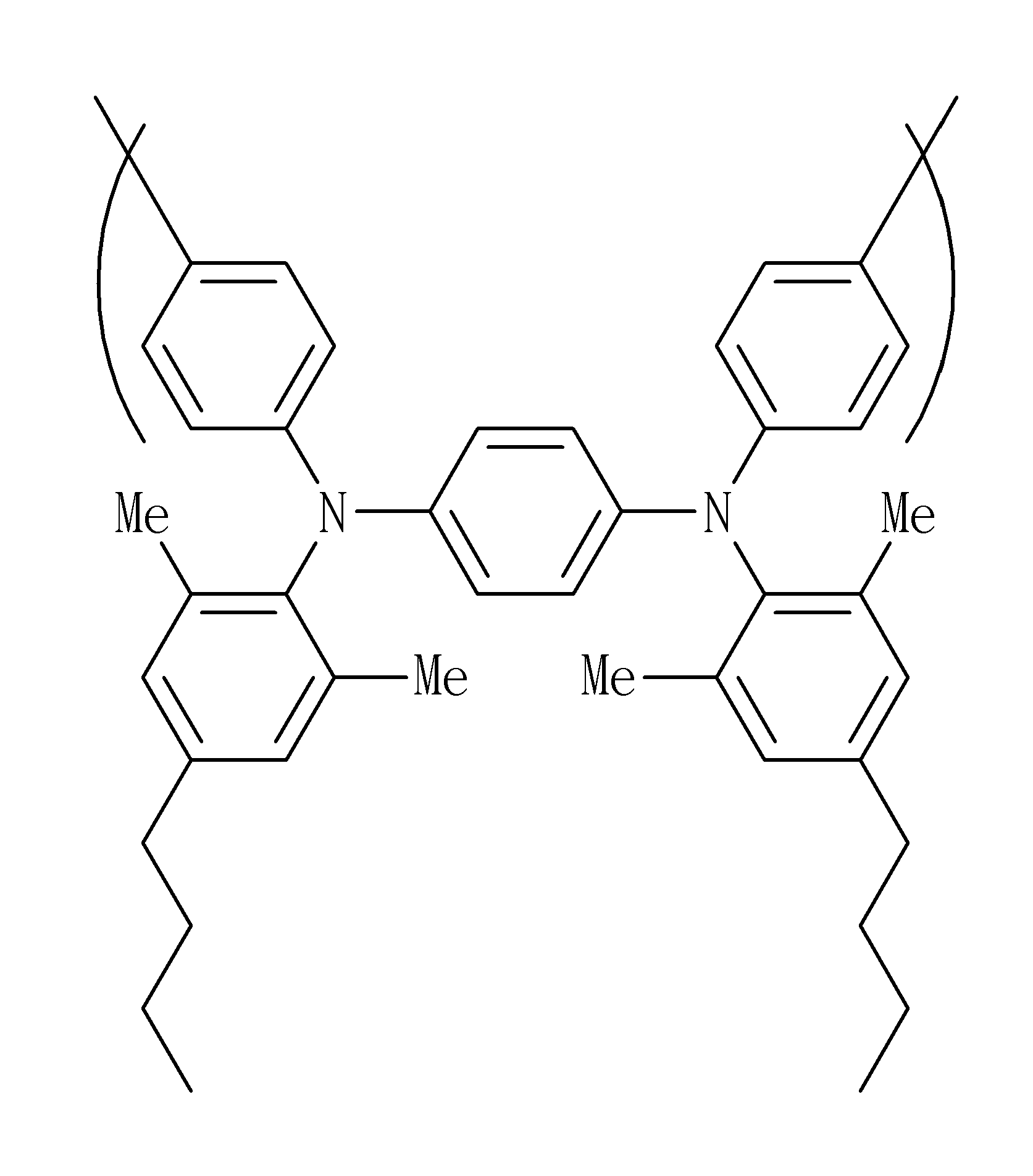
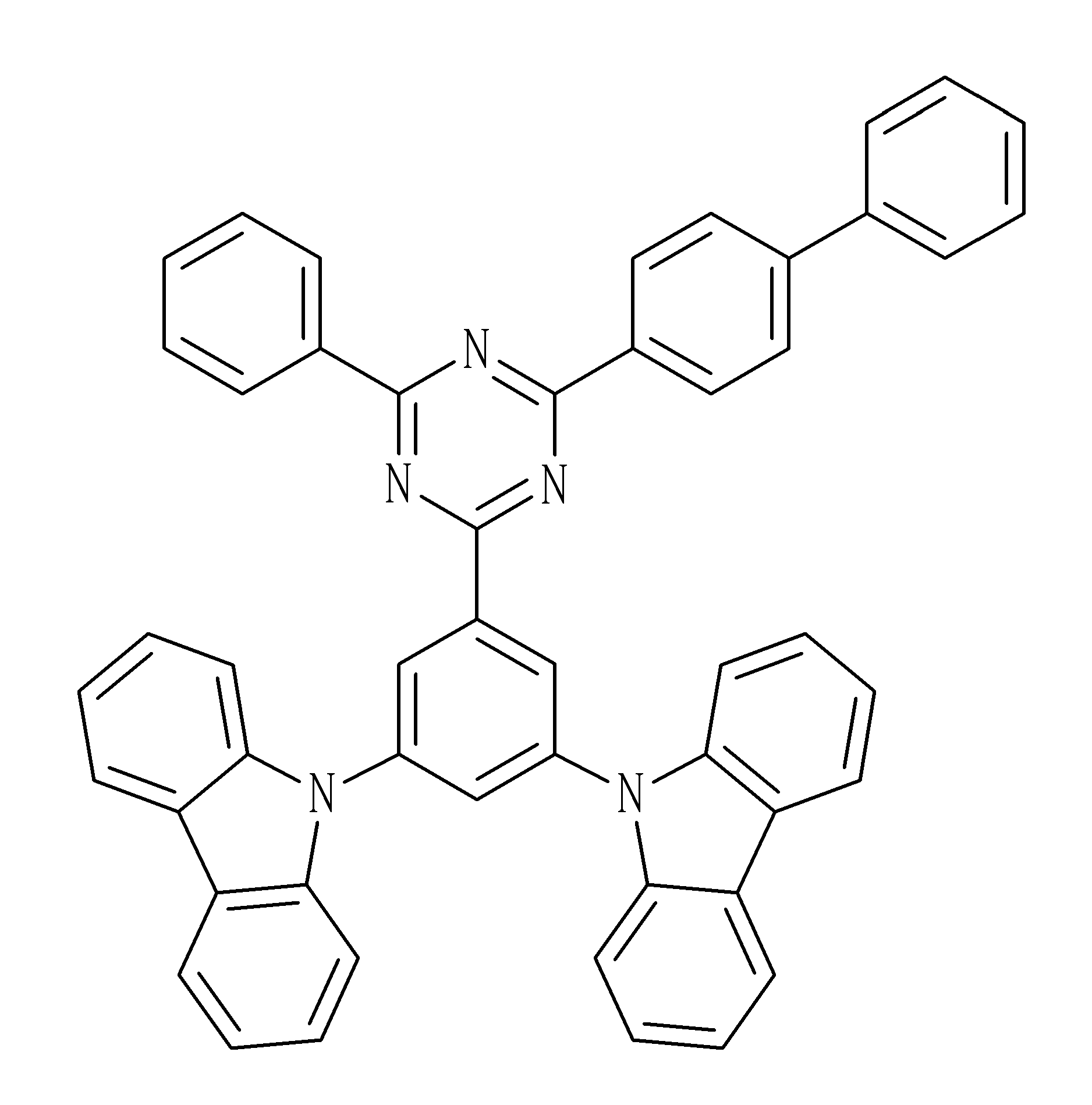
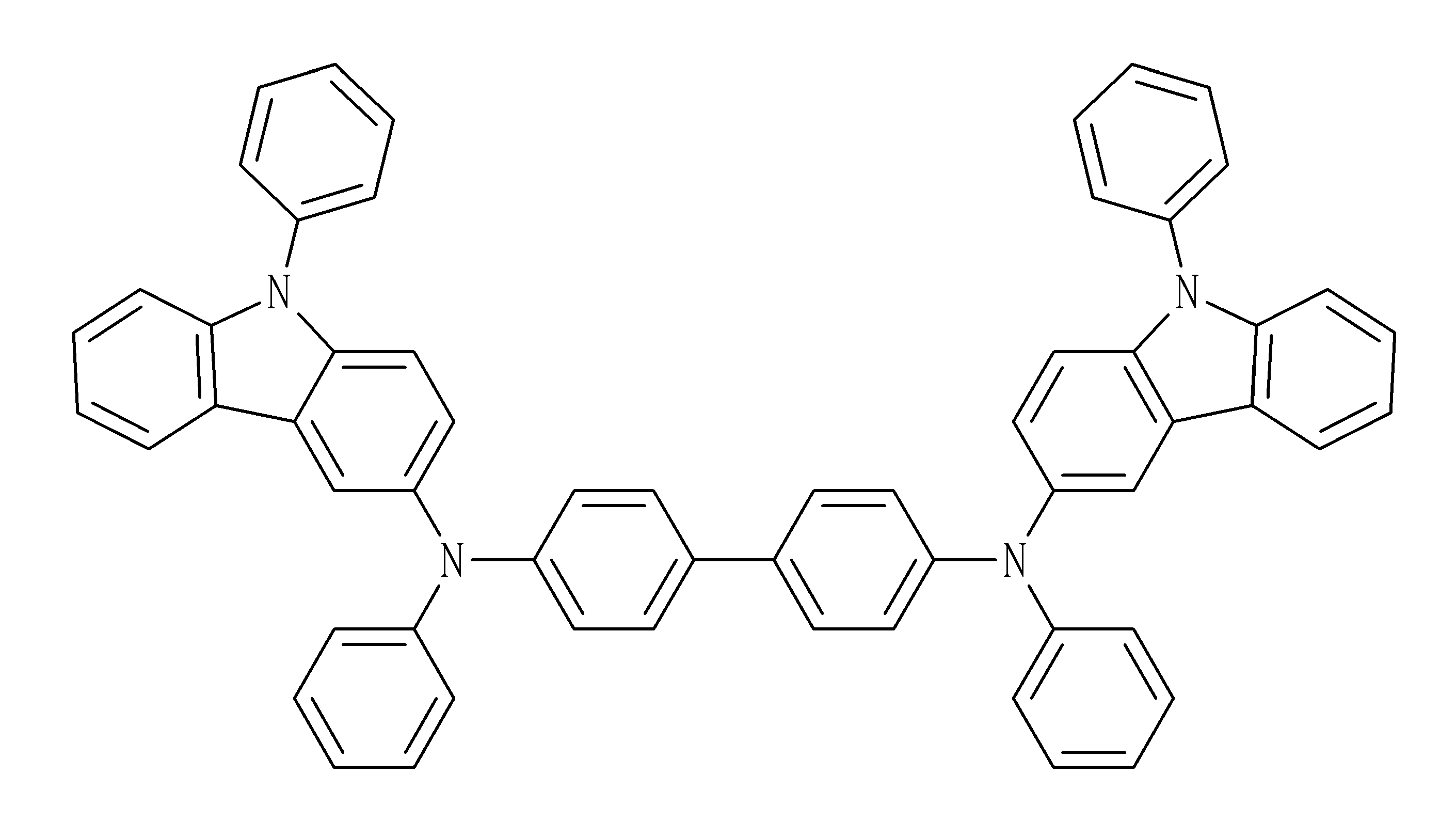
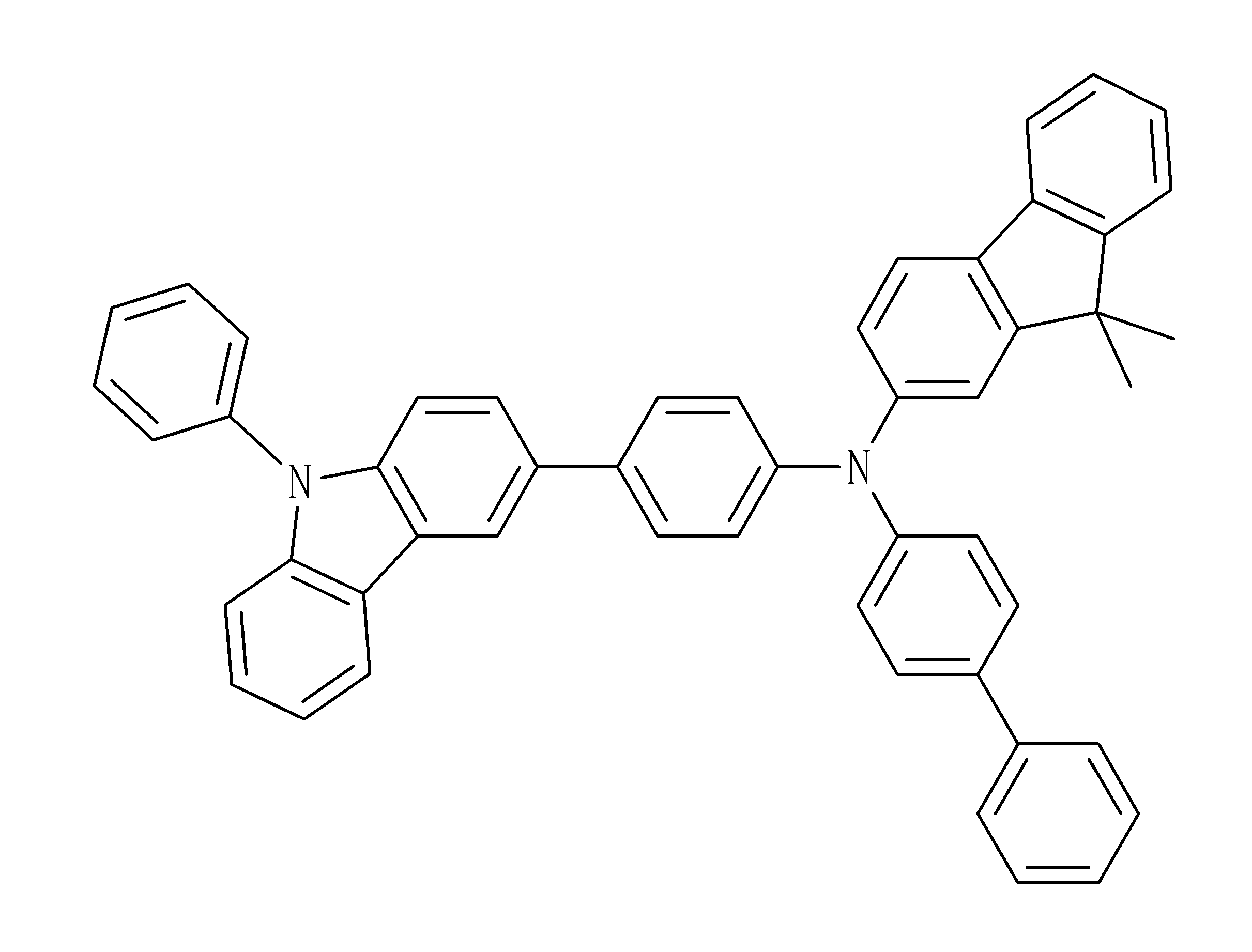
본 발명의 일 실시예에 따르면, 정공 수송층(215)은 하기 화학식 1로 표현되는 화합물, 하기 화학식 2로 표현되는 화합물, 하기 화학식 3으로 표현되는 화합물 및 하기 화학식 4로 표현되는 화합물을 포함하는 정공 수송층 형성용 조성물에 의해 만들어질 수 있다.According to one embodiment of the present invention, the
[화학식 1][Formula 1]

[화학식 2][Formula 2]

[화학식 3][Formula 3]
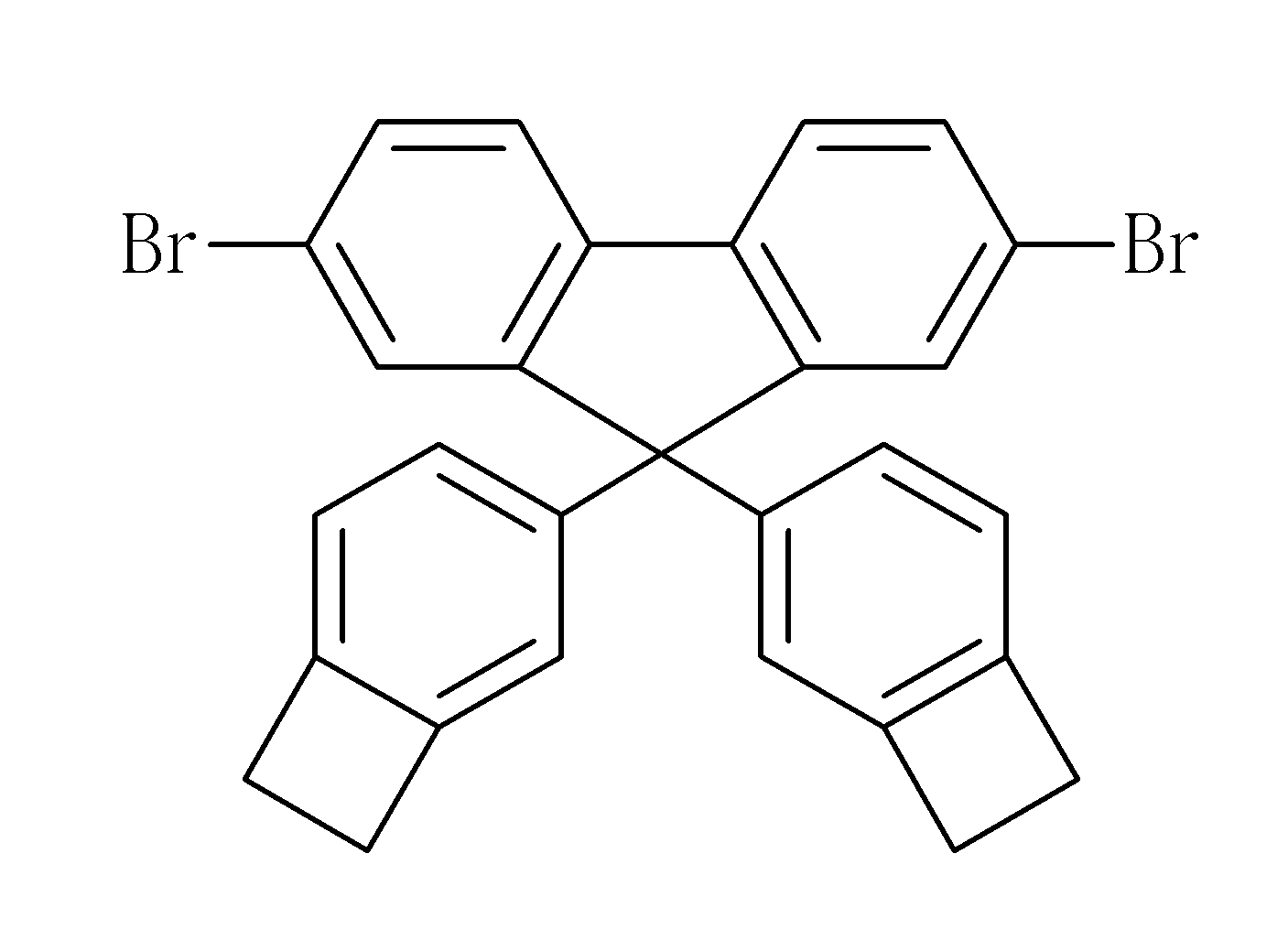
[화학식 4][Formula 4]

즉, 정공 수송층(215)은 화학식 1로 표현되는 화합물, 화학식 2로 표현되는 화합물, 화학식 3으로 표현되는 화합물 및 화학식 4로 표현되는 화합물을 포함할 수 있다. 예를 들어, 화학식 1로 표현되는 화합물, 화학식 2로 표현되는 화합물, 화학식 3으로 표현되는 화합물 및 화학식 4로 표현되는 화합물을 포함하는 정공 수송층 형성용 조성물의 코팅 및 경화에 의해 정공 수송층(215)이 만들어질 수 있다.That is, the
정공 수송층 형성용 조성물은 화학식 1로 표현되는 화합물 25 내지 35 중량%, 화학식 2로 표현되는 화합물 10 내지 15 중량%, 화학식 3으로 표현되는 화합물 5 내지 10 중량% 및 화학식 4로 표현되는 화합물 40 내지 60 중량%를 포함할 수 있다.The composition for forming a hole transport layer includes 25 to 35% by weight of the compound represented by
정공 수송층 형성용 조성물은 용액 상태일 수 있다. 용액을 이용하여 막을 형성하는 방법을 "용액법" 또는 "습식법" 이라고도 한다. 본 발명의 일 실시예에 따르면 정공 수송층(215)은 용액법으로 만들어질 수 있다.The composition for forming a hole transport layer may be in a solution state. The method of forming a film using a solution is also called the “solution method” or “wet method.” According to one embodiment of the present invention, the
정공 수송층 형성용 조성물이 용액 상태이기 때문에, 정공 수송층(215) 하부에 입자 또는 불순물이 존재하더라도 유기 발광층(212)과 접촉하는 정공 수송층(215)의 일면이 평탄해질 수 있다. 그에 따라, 유기 발광층(212)의 발광 효율이 향상될 수 있고 수명이 증가될 수 있다.Since the composition for forming the hole transport layer is in a solution state, even if particles or impurities exist in the lower part of the
예를 들어, 제1 전극(211)의 형성 과정에서 발생된 패터닝 잔사가 제1 전극(211) 표면에 붙어 있거나, 또는 다른 막 형성 과정에서 발생된 잔사 또는 입자들이 제1 전극(211) 상부에 잔존하는 경우, 표면 불균일 및 막 손상이 유발될 수 있다. 이러한 표면 불균일에 의해 유기 발광층(212)에서 발광 불량이 발생할 수 있고, 유기발광소자(210)의 수명이 단축될 수 있다.For example, patterning residues generated during the formation process of the
그러나, 본 발명의 일 실시예에 따르면, 정공 수송층(215)은 용액법으로 만들어지기 때문에, 정공 수송층(215) 하부 표면이 불균일하더라도 유기 발광층(212)과 접촉하는 정공 수송층(215)의 상부 표면이 평탄해질 수 있다. 그에 따라, 유기 발광층(212)에서의 발광 불량이 방지될 수 있고, 유기발광소자(210)의 수명이 연장될 수 있다.However, according to one embodiment of the present invention, since the
유기 발광층(212)은 정공 수송층(215) 상에 배치된다. 유기 발광층(212)은 제1 전극(211)과 중첩한다. The organic light-emitting
유기 발광층(212)은 단분자 또는 고분자 유기물로 만들어질 수 있다. 본 발명의 일 실시예에 따르면, 유기 발광층(212)은 호스트 및 발광성 도펀트를 포함할 수 있다. 유기 발광층(212)을 구성하는 호스트와 발광성 도펀트를 유기 발광 물질이라 한다.The organic
유기 발광층(212)은 유기 발광 물질의 증착에 의해 만들어질 수 있다. 구체적으로, 유기 발광층(212)은 호스트와 발광성 도펀트의 증착에 의하여 만들어질 수있다.The organic light-emitting
제2 전극(213)은 유기 발광층(212) 상에 배치된다. 도 2를 참조하면, 제2 전극(213)은 유기 발광층(212)뿐만 아니라 화소 정의막(190) 위에도 배치된다. The
제2 전극(213)은 마그네슘(Mg), 은(Ag), 금(Au), 칼슘(Ca), 리튬(Li), 크롬(Cr), 구리(Cu) 및 알루미늄(Al) 중 하나 이상의 금속을 포함하는 반투과막으로 만들어진다. 일반적으로 반투과막은 200nm 미만의 두께를 가질 수 있다. 반투과막의 두께가 얇아질수록 빛의 투과율이 높아지고, 두께가 두꺼워질수록 빛의 투과율이 낮아진다.The
본 발명의 일 실시예에 따르면, 제2 전극(213)은 마그네슘(Mg)과 은(Ag)을 포함하며, 은(Ag)의 함량이 마그네슘(Mg)의 함량보다 많다. According to one embodiment of the present invention, the
이하, 도 3을 참조하여 유기발광 표시장치(101)의 공진을 설명한다.Hereinafter, resonance of the organic light emitting
도 3을 참조하면, 제1 전극(211)은 반사막(211a) 및 반사막(211a) 상에 배치된 광투과성 도전막(211b)을 포함한다. Referring to FIG. 3, the
유기발광 표시장치(101)는 다층의 적층구조를 가지며, 유기 발광층(212)에서 발생된 빛은 다층의 적층구조를 통과하여 방출된다. The organic light emitting
두 개의 반사면 사이에서 빛이 반사를 반복하면 광학적 공진이 발생될 수 있다. 광학적 공진이 발생하면, 빛의 에너지가 증가되고, 증가된 에너지를 갖는 빛은 다층의 적층 구조를 용이하게 통과하여 외부로 방출될 수 있다. 이와 같이 두 개의 반사층 사이에서 빛이 공진될 수 있도록 만들어진 구조를 공진 구조라 하고, 공진이 이루어지는 두 개의 반사층 사이의 거리를 공진 거리라 한다. 공진 거리는 빛의 파장에 따라 달라진다.Optical resonance can occur when light is repeatedly reflected between two reflective surfaces. When optical resonance occurs, the energy of light increases, and light with increased energy can easily pass through the multi-layer laminated structure and be emitted to the outside. In this way, a structure made so that light can resonate between two reflective layers is called a resonance structure, and the distance between the two reflective layers where resonance occurs is called a resonance distance. The resonance distance varies depending on the wavelength of light.
본 발명의 일 실시예에 따르면, 유기 발광층(212)을 사이에 두고 대향하는 반사막(211a)의 상부 표면(211s)과 제2 전극(213)의 하부 표면(213s)이 반사면이 될 수 있다.According to an embodiment of the present invention, the
유기 발광층(212)에서 발생되는 빛의 피크 파장이 "λ1"이고, 반사막(211a)의 상부 표면(211s)과 제2 전극(213)의 하부 표면(213s) 사이의 광학적 거리가 "L1"이고, 유기 발광층(212)에서 발생되는 빛이 반사막(211a)의 상부 표면(211s)과 제2 전극(213)의 하부 표면(213s) 사이에서 반사할 때에 생기는 위상 시프트를 Ф라디안이라 할 때, 다음 식 1을 만족하는 범위에서 L1이 양(+)의 최소치가 되도록 설정될 수 있다.The peak wavelength of light generated from the organic
[식 1][Equation 1]
(2L1)/λ+Ф/(2π) = m (m은 정수) (2L1)/λ+Ф/(2π) = m (m is an integer)
또한, 유기 발광층(212)에서 발생되는 빛의 피크 파장이 "λ1"이고, 반사막(211a)의 상부 표면(211s)과 제2 전극(213)의 하부 표면(213s) 사이의 광학적 거리가 "L1"일 때, 공진을 위해 다음 식 2를 만족하도록 L1이 조정될 수 있다. In addition, the peak wavelength of light generated from the organic
[식 2][Equation 2]
L1 = [(2m+1)/4] x λ1L1 = [(2m+1)/4] x λ1
여기서, m은 0 이상의 정수이다.Here, m is an integer greater than or equal to 0.
또한, 광학적 거리 L1은 다음 식 3으로 구해질 수 있다.Additionally, the optical distance L1 can be obtained by the following equation 3.
[식 3][Equation 3]
L1 = d1 x n1L1 = d1 x n1
여기서, d1은 반사막(211a)의 상부 표면(211s)과 제2 전극(213)의 하부 표면(213s) 사이의 거리이고, n1은 반사막(211a)의 상부 표면(211s)과 제2 전극(213)의 하부 표면(213s) 사이의 평균 굴절률이다.Here, d1 is the distance between the
정공 수송층(215)이 작은 굴절률을 가지는 경우, 정공 수송층(215)이 큰 두께를 가지더라도 공진 거리가 확보될 수 있다. 본 발명의 일 실시예에 따르면, 정공 수송층(215)은 1.6 이하의 굴절률을 가질 수 있다. 정공 수송층(215)은, 예를 들어 1.4 내지 1.6의 낮은 굴절률을 가질 수 있다. 그에 따라, 정공 수송층(215)이 비교적 큰 두께를 가질 수 있다. When the
정공 수송층(215)의 두께가 크면 정공 수송층(215)의 우수한 표면 평탄화 특성을 가질 수 있다. 그에 따라, 그에 따라, 유기 발광층(212)의 발광 효율이 향상될 수 있다.If the
예를 들어, 정공 수송층(215)은 5 내지 10nm의 두께를 가질 수 있다. 또한, 정공 수송층(215)은 100 내지 110nm의 두께를 가질 수도 있다. 정공 수송층(215)이 5 내지 10nm의 두께를 가지는 경우, 유기 발광층(212)에서 발생된 빛의 1차 공진이 유도될 수 있다. 정공 수송층(215)은 100 내지 110nm의 두께를 가지는 경우, 유기 발광층(212)에서 발생된 빛의 2차 공진이 유도될 수 있다.For example, the
도 4는 본 발명의 다른 일 실시예에 따른 유기발광 표시장치(102)의 단면도이다. 이하, 중복을 피하기 위하여 이미 설명된 구성요소에 대한 설명은 생략된다.Figure 4 is a cross-sectional view of an organic light emitting
본 발명의 다른 일 실시예에 따른 유기발광 표시장치(102)는 유기 발광층(212)과 제2 전극(213) 사이에 배치된 전자 수송층(electron transport layer; ETL)(217)을 포함한다.The organic light emitting
전자 수송층(217)은 화학식 5로 표현되는 화합물 및 화학식 6으로 표현되는 화합물 중 적어도 하나의 증착에 의하여 만들어질 수 있다.The
[화학식 5][Formula 5]
[화학식 6][Formula 6]
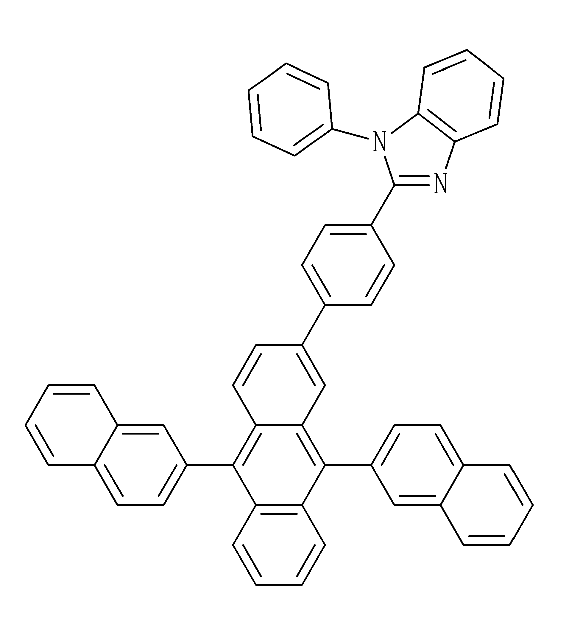
도 4에 도시되지 않았지만, 전자 수송층(217) 상에 전자 주입층(electron injection layer, EIL)이 배치될 수 있다.Although not shown in FIG. 4, an electron injection layer (EIL) may be disposed on the
도 5는 본 발명의 또 다른 일 실시예에 따른 유기발광 표시장치(103)의 단면도이다. Figure 5 is a cross-sectional view of an organic light emitting
본 발명의 또 다른 일 실시예에 따른 유기발광 표시장치(103)는 제1 전극(211)과 정공 수송층(215) 사이에 배치된 정공 주입층(hole injection layer; HIL) (214)을 포함한다.The organic light emitting
정공 주입층(214)은 정공 수송층(215)과 마찬가지로 용액법으로 만들어질 수 있다. 예를 들어, PEDOT/PSS 용액이 제1 전극(211)에 코팅된 후 경화되여 정공 주입층(214)이 만들어질 수 있다. 이러한 정공 주입층(214)은 1.5의 굴절률을 가질 수 있으며 12nm의 두께를 가질 수 있다.Like the
도 5를 참조하면, 정공 주입층(214)은 제1 전극(211) 상부에 배치된다. 그러나, 본 발명의 또 다른 일 실시예가 이에 한정되는 것은 아니며, 정공 주입층(214)은 제1 전극(211) 상부뿐만 아니라 화소 정의막(190)의 상부 에도 배치될 수 있다.Referring to FIG. 5 , the
도 6은 본 발명의 또 다른 일 실시예에 따른 유기발광 표시장치(104)의 단면도이다.Figure 6 is a cross-sectional view of an organic light emitting
도 6을 참조하면, 유기발광소자(210)를 보호하기 위해 제2 전극(213) 상에 박막봉지층(300)이 배치된다. 박막봉지층(300)은 수분이나 산소와 같은 외기가 유기발광소자(210)로 침투하는 것을 방지한다. Referring to FIG. 6, a thin
박막봉지층(300)은 교호적으로 배치된 적어도 하나의 무기막(311, 312) 및 적어도 하나의 유기막(321)을 포함한다. The thin
도 6에 도시된 박막봉지층(300)은 2개의 무기막(311, 312)과 1개의 유기막(321)을 포함하고 있다. 그러나, 박막봉지층(300)의 구조가 도 6에 의해 한정되는 것은 아니다.The thin
무기막(311, 312)은 금속 산화물, 금속 산질화물, 실리콘 산화물, 실리콘 질화물 및 실리콘 산질화물 중 적어도 하나를 포함할 수 있다.The
무기막(311, 312)은 화학증착(chemical vapor deposition, CVD)법 또는 원자층 증착(atomic layer depostion, ALD)법을 통해 형성된다. 하지만, 본 발명의 일 실시예가 이에 한정되는 것은 아니며, 무기막(311, 312)은 해당 기술 분야의 종사자에게 공지된 다양한 방법을 통해 형성될 수 있다.The
유기막(321)은, 예를 들어, 고분자(polymer) 계열의 소재로 만들어질 수 있다.The
유기막(321)은 열증착 공정을 통해 형성될 수 있다. 유기막(321)을 형성하기 위한 열증착 공정은 유기발광소자(210)를 손상시키지 않는 온도 범위 내에서 진행된다. 하지만, 본 발명의 일 실시예가 이에 한정되는 것은 아니며, 유기막(321)은 해당 기술 분야의 종사자에게 공지된 다양한 방법을 통해 형성될 수 있다.The
박막의 밀도가 치밀하게 형성된 무기막(311, 312)이 주로 수분 또는 산소의 침투를 억제한다. 대부분의 수분 및 산소는 무기막(311, 312)에 의해 유기발광소자(210)로의 침투가 차단된다.The
무기막(311, 312)을 통과한 수분 및 산소는 유기막(321)에 의해 다시 차단된다. 유기막(321)은 투습 억제 외에 무기막(311, 312)과 무기막(311, 312) 사이에서, 각 층들 간의 응력을 줄여주는 완충층의 역할도 함께 수행한다. 또한, 유기막(321)은 평탄화 특성을 가지므로, 유기막(321)에 의해 박막봉지층(300)의 최상부면이 평탄해질 수 있다.Moisture and oxygen that have passed through the
박막봉지층(300)은 50㎛ 이하의 두께를 가질 수 있으며, 필요한 경우 10㎛ 이하의 두께를 가질 수도 있다. 따라서, 매우 얇은 두께를 갖는 유기발광 표시장치(104)가 만들어질 수 있다. 이러한 유기발광 표시장치(104)는 우수한 플렉서블 특성을 가질 수 있다.The thin
그러나, 본 발명의 다른 일 실시예가 이에 한정되는 것은 아니다. 유기발광소자(210)를 보호하기 위해, 유기발광소자(210) 상에 박막봉지층(300) 대신 봉지 기판(미도시)이 배치될 수도 있다. 봉지 기판은 유리, 석영, 세라믹, 및 플라스틱 등의 투명 절연성 재료로 만들어질 수 있다. 봉지 기판은 기판(110)과 합착 밀봉되어 유기발광소자(210)를 보호한다. However, another embodiment of the present invention is not limited to this. In order to protect the organic
또한, 유기발광소자(210)와 봉지 기판 사이에 충진제(미도시)가 배치될 수도 있다. 충진제는 유기 물질, 예를 들어, 폴리머로 형성될 수 있다. 또한, 유기발광소자(210) 상에 금속 또는 무기물로 된 보호층 또는 봉지층이 배치되어, 유기발광소자(210)를 보호할 수도 있다.Additionally, a filler (not shown) may be disposed between the organic
도 7은 본 발명의 또 다른 일 실시예에 따른 유기발광 표시장치(105)의 단면도이다. Figure 7 is a cross-sectional view of an organic light emitting
도 7에 도시된 유기발광 표시장치(105)의 제1 전극(211)은 반사막(211a) 및 광투과성 도전막(211b)을 포함한다. 반사막(211a)은 마그네슘(Mg), 은(Ag), 금(Au), 칼슘(Ca), 리튬(Li), 크롬(Cr), 구리(Cu) 및 알루미늄(Al) 중 하나 이상의 금속을 포함할 수 있다. 광투과성 도전막(211b)은 투명도전성산화물(TCO)로 만들어질 수 있다. 투명도전성산화물(TCO)의 예로, ITO(Indium Tin Oxide), IZO(Indium Zinc Oxide), ZnO(Zinc Oxide), AZO(Aluminum Zinc Oxide) 및 In2O3(Indium Oxide) 등이 있다. The
도 7에 도시된 유기발광 표시장치(105)는 제1 전극(211)과 정공 수송층(215) 사이에 배치된 정공 주입층(HIL) (214)을 포함한다. 정공 주입층(214)은 PEDOT/PSS 용액에 의해 만들어질 수 있다. The organic light emitting
또한, 도 7에 도시된 유기발광 표시장치(107)는 유기 발광층(212) 상에 배치된 전자 수송층(electron transport layer; ETL)(217) 및 전자 수송층(217) 상에 배치된 전자 주입층(216)을 포함한다.In addition, the organic light emitting display device 107 shown in FIG. 7 includes an electron transport layer (ETL) 217 disposed on the organic
전자 수송층(217)은 화학식 5로 표현되는 화합물 및 화학식 6으로 표현되는 화합물 중 적어도 하나의 증착에 의하여 만들어질 수 있다. 전자 주입층(216)은 Liq(lithium quinolate)의 증착에 의하여 만들어질 수 있다.The
또한, 도 7을 참조하면, 제2 전극(213) 상에 캡핑층(230)이 배치된다. 캡핑층(230)은 유기발광소자(210)를 보호하며, 유기 발광층(212)에서 발생된 빛이 효율적으로 외부로 방출될 수 있도록 돕는 역할을 한다. 캡핑층(230)은 광투과성을 갖는 무기 물질 및 유기 물질 중 적어도 하나를 포함할 수 있다.Additionally, referring to FIG. 7 , a
도 8은 정공 수송층(215)의 굴절률 및 소광 계수에 대한 그래프이다. Figure 8 is a graph of the refractive index and extinction coefficient of the
구체적으로 도 8은, 화학식 1로 표현되는 화합물, 화학식 2로 표현되는 화합물, 화학식 3으로 표현되는 화합물 및 화학식 4로 표현되는 화합물을 포함하는 정공 수송층 형성용 조성물로 만들어진 정공 수송층(215)의 굴절률(n) 및 소광계수(k)를 측정한 결과를 나타낸다. 이 때, 빛의 파장에 따라 굴절률이 측정되었다.Specifically, Figure 8 shows the refractive index of the
도 8을 참조하면, 정공 수송층(215)은 가시광선 파장대의 빛에 대하여 약 1.4 정도의 굴절률(n)을 가지며, 0의 소광계수(k)를 갖는다. Referring to FIG. 8, the
이하, 도 9a 내지 9i를 참조하여 본 발명의 또 다른 일 실시예에 따른 유기발광 표시장치(105)의 제조방법을 설명한다.Hereinafter, a method of manufacturing an organic light emitting
구체적으로, 도 9a 내지 9i는 도 7에 도시된 유기발광 표시장치(105)의 제조 공정에 대한 단면도이다.Specifically, FIGS. 9A to 9I are cross-sectional views of the manufacturing process of the organic light emitting
도 9a를 참조하면, 기판(110) 상에 제1 전극(211)이 형성된다. 보다 구체적으로, 기판(110) 상에 버퍼층(120) 및 배선부(130)가 형성되고, 그 위에 제1 전극(211)이 형성된다. 제1 전극(211)은 배선부(130)에 배치된 구동 박막 트랜지스터(20)와 연결된다. Referring to FIG. 9A, a
제1 전극(211)은 반사막(211a) 및 광투과성 도전막(211b)을 포함한다.The
도 9b를 참조하면, 기판(110) 상에 화소 정의막(190)이 형성된다.Referring to FIG. 9B, a
화소 정의막(190)은 복수개의 제1 전극(211)들을 서로 구분하는 역할을 한다. 화소 정의막(190)은 개구부(195)를 갖는다. 화소 정의막(190)의 개구부(195)는 제1 전극(211)의 일부를 드러낸다.The
도 9c를 참조하면, 제1 전극(211) 및 화소 정의막(190) 상에 정공 주입층(214)이 형성된다. 정공 주입층(214)은 제1 전극(211) 상부에만 배치될 수 있다.Referring to FIG. 9C, a
정공 주입층(214)은 PEDOT/PSS 용액에 의해 만들어질 수 있다. PEDOT/PSS 용액으로, 예를 들어, PEDOT 함량이 0.5 중량%이고, PSS 함량이 0.8 중량%인 수용액(용매 H2O)이 사용될 수 있다. The
정공 주입층(214)은 1.5의 굴절률을 가질 수 있으며 12nm의 두께를 가질 수 있다.The
도 9d를 참조하면, 정공 주입층(214) 상에 정공 수송층(215)이 형성된다.Referring to FIG. 9D, a
정공 수송층 형성용 조성물이 정공 주입층(214) 상에 코팅 및 경화되어 정공 수송층(215)이 형성될 수 있다. The hole transport layer forming composition may be coated and cured on the
정공 수송층 형성용 조성물은 화학식 1로 표현되는 화합물, 화학식 2로 표현되는 화합물, 화학식 3으로 표현되는 화합물 및 화학식 4로 표현되는 화합물을 포함한다. 보다 구체적으로, 정공 수송층 형성용 조성물은 화학식 1로 표현되는 화합물 25 내지 35 중량%, 화학식 2로 표현되는 화합물 10 내지 15 중량%, 화학식 3으로 표현되는 화합물 5 내지 10 중량% 및 화학식 4로 표현되는 화합물 40 내지 60 중량%를 포함할 수 있다.The composition for forming a hole transport layer includes a compound represented by
도 9e를 참조하면, 정공 수송층(215) 상에 유기 발광층(212)이 형성된다. 유기 발광층(212)은 제1 전극(211)과 중첩한다. Referring to FIG. 9E, the organic light-emitting
유기 발광층(212)은 유기 발광 물질의 증착에 의하여 만들어진다. 즉, 호스트 및 발광성 도펀트 물질의 증착에 의하여 유기 발광층(212)이 만들어진다.The organic light-emitting
도 9f를 참조하면, 유기 발광층(212) 상에 전자 수송층(217)이 형성된다.Referring to FIG. 9F, an
전자 수송층(217)은 화학식 5로 표현되는 화합물 및 화학식 6으로 표현되는 화합물 중 적어도 하나의 증착에 의하여 만들어질 수 있다.The
도 9g를 참조하면, 전자 수송층(217) 상에 전자 주입층(216)이 형성된다.Referring to FIG. 9g, an
전자 수송층(217) 상에 Liq(lithium quinolate)가 증착되어 전자 주입층(216)이 만들어질 수 있다.Lithium quinolate (Liq) may be deposited on the
도 9h를 참조하면, 전자 주입층(216) 상에 제2 전극(213)이 배치된다. 그에 따라 유기발광소자(210)가 만들어진다.Referring to FIG. 9H, the
제2 전극(213)은 반투과막으로 만들어질 수 있으며, 10 내지 20nm의 두께를 가질 수 있다.The
도 9i를 참조하면, 제2 전극(213) 상에 캡핑층(230)이 형성된다. Referring to FIG. 9I, a
캡핑층(230)은 유기발광소자(210)를 보호하며, 유기 발광층(212)에서 발생된 빛이 효율적으로 외부로 방출될 수 있도록 돕는 역할을 한다.The
캡핑층(230)은 광투과성을 갖는 무기 물질 및 유기 물질 중 적어도 하나를 포함할 수 있다. 캡핑층(230)은 30nm 내지 300nm의 두께를 가질 수 있으며, 300nm 이상의 두께를 가질 수도 있다. 캡핑층(230)이 두꺼울수록 유기발광소자(210)의 보호에 유리하다. 그러나, 캡핑층(230)이 두꺼우면 유기발광 표시장치(105)의 박막화에 불리하다.The
캡핑층(230)은 당업계에서 알려진 방법으로 만들어질 수 있다. 증착에 의하여 캡핑층(230)이 만들어질 수도 있다. 예를 들어, 캡핑층(230)은 하기 화학식 7로 표현되는 화합물의 증착에 의하여 만들어질 수 있으며, 60nm의 두께를 가질 수 있다.The
[화학식 7][Formula 7]
이하, 시험예 및 비교예를 설명한다.Hereinafter, test examples and comparative examples will be described.
<시험예 1><Test Example 1>
스퍼터링 및 패터닝에 의해, 유리로 된 기판(110) 상에 100nm 두께의 은(Ag) 층과 20nm 두께의 ITO 층이 순차적으로 적층된 제1 전극(211)을 형성하였다. 은(Ag) 층은 반사막(211a)이고, 20nm 두께의 ITO 층은 광투과성 도전막(211b)이다. By sputtering and patterning, a
다음, 이소프로필 알코올(IPA)을 이용하여 반사막(211a)과 광투과성 도전막(211b)을 초음파 세척하고, 세정 및 건조하고, 다시 초음파 세정 및 전처리 (UV-O3 처리, 열처리) 하였다. 이와 같이 제조된 제1 전극(211)은 양극이다.Next, the
PEDOT/PSS 용액을 이용하여 제1 전극(211) 상에 12nm의 두께 정공 주입층(214)을 형성하였다. PEDOT/PSS 용액으로 0.5 중량%의 PEDOT 및 0.8 중량%의 PSS를 포함하는 수용액(용매 H2O)이 사용되었다. 정공 주입층(214)의 굴절률은 1.5이다.A
정공 수송층 형성용 조성물(WHT1)을 이용하여 정공 주입층(214) 상에 5nm 두께의 정공 수송층(215)을 형성하였다.A 5 nm thick
정공 수송층 형성용 조성물은 화학식 1로 표현되는 화합물 3 중량%, 화학식 2로 표현되는 화합물 12.5 중량%, 화학식 3으로 표현되는 화합물 7.5 중량% 및 화학식 4로 표현되는 화합물 50 중량%를 포함하는 용액이다. 시험예 1에 따르면 정공 수송층(215)은 용액법으로 형성된다.The composition for forming a hole transport layer is a solution containing 3% by weight of the compound represented by
정공 수송층(215) 상에 유기 발광층(212)을 형성하였다. 호스트 및 발광성 도펀트 물질의 증착에 의하여 유기 발광층(212)을 형성하였다. 화학식 8로 표현되는 안트라센 유도체 화합물이 호스트로 사용되었고, 도펀트 물질로 화학식 9로 표현되는 화합물이 사용되었다. 도펀트 물질은 전체 증착 재료에 대해 5 부피%로 사용되었다.An organic light-emitting
시험예 1에 따르면 유기 발광층(212)은 30nm의 두께를 갖는다.According to Test Example 1, the
[화학식 8][Formula 8]

[화학식 9] [Formula 9]

다음, 유기 발광층(212) 상에 화학식 5로 표현되는 화합물을 20nm의 두께로 증착하여 전자 수송층(217)을 형성하였다. Next, the compound represented by Chemical Formula 5 was deposited on the
다음, 전자 수송층(217) 상에 Liq(lithium quinolate)를 0.35nm의 두께로 증착하여 전자 주입층(216)을 형성하였다.Next, lithium quinolate (Liq) was deposited to a thickness of 0.35 nm on the
전자 주입층(216) 상에 은(Ag)과 마그네슘(Mg)을 공증착(체적비 80:20)하여 제2 전극(213)을 형성하였다. 시험예 1의 제2 전극(213)은 13nm의 두께를 가진다. The
제2 전극(213)은 반투과막이며, 음극이다.The
제2 전극(213) 상에 화학식 7로 표현되는 화합물을 60nm의 두께로 증착하여 캡핑층(230)을 형성하였다.A
이와 같이 제조된 유기발광소자 시료(시험예 1)에 10mA/cm2의 전류 밀도로 전류가 인가될 때, 구동 전압(V)과 전류 효율(cd/A, 발광 효율)을 각각 평가하였다. 그 결과는 하기 표 1에 개시되어 있다.When a current was applied to the organic light emitting device sample (Test Example 1) manufactured in this way at a current density of 10 mA/cm 2 , the driving voltage (V) and current efficiency (cd/A, luminous efficiency) were evaluated, respectively. The results are disclosed in Table 1 below.
<시험예 2><Test Example 2>
시험예 1과 동일한 방법으로 유기발광소자 시료를 제조하되, 다만, 정공 주입층(214)은 70nm의 두께, 정공 수송층(215)은 105nm의 두께, 유기 발광층(212)은 38nm의 두께로 형성되었다.An organic light emitting device sample was prepared in the same manner as Test Example 1, except that the
이와 같이 제조된 시험예 2의 유기발광소자 시료(시험예 2)에 10mA/cm2의 전류 밀도로 전류가 인가될 때, 구동 전압(V)과 전류 효율(cd/A, 발광 효율)을 각각 평가하였다. 그 결과는 하기 표 1에 개시되어 있다.When a current is applied to the organic light emitting device sample (Test Example 2) prepared in this way at a current density of 10 mA/cm 2 , the driving voltage (V) and current efficiency (cd/A, luminous efficiency) are respectively evaluated. The results are disclosed in Table 1 below.
<시험예 3><Test Example 3>
시험예 1과 동일한 방법으로 유기발광소자 시료를 제조하되, 다만, 시험예 1의 정공 수송층 형성용 조성물(WHT1)을 이용하여 1.4의 굴절률 및 12nm의 두께 두께를 갖는 정공 주입층(214)을 형성하고, 그 위에 5nm의 두께를 갖는 정공 수송층(215)을 형성하였다. 유기 발광층(212)은 시험예 1과 동일하며 30nm의 두께를 가지도록 제조되었다.An organic light emitting device sample was prepared in the same manner as Test Example 1, except that the
이와 같이 제조된 시험예 3의 유기발광소자 시료(시험예 3)에 10mA/cm2의 전류 밀도로 전류가 인가될 때, 구동 전압(V)과 전류 효율(cd/A, 발광 효율)을 각각 평가하였다. 그 결과는 하기 표 1에 개시되어 있다.When a current is applied to the organic light-emitting device sample (Test Example 3) prepared in this way at a current density of 10 mA/cm 2 , the driving voltage (V) and current efficiency (cd/A, luminous efficiency) are respectively evaluated. The results are disclosed in Table 1 below.
<비교예 1><Comparative Example 1>
제1 전극(211) 상에 화학식 7로 표현되는 화합물을 증착하여 5nm 두께를 갖는 정공 주입층(214)을 형성하고, 그 위에 화학식 10으로 표현되는 화합물을 증착하여 5nm 두께를 갖는 정공 수송층(215)을 형성하는 것을 제외하고 시험예 1과 동일한 방법으로 유기발광소자 시료(비교예 1)를 제조하였다.The compound represented by Formula 7 is deposited on the
[화학식 10][Formula 10]
이와 같이 제조된 비교예 1의 유기발광소자 시료(비교예 1)에 10mA/cm2의 전류 밀도로 전류가 인가될 때, 구동 전압(V)과 전류 효율(cd/A, 발광 효율)을 각각 평가하였다. 그 결과는 하기 표 1에 개시되어 있다.When a current is applied to the organic light emitting device sample (Comparative Example 1) manufactured in this way at a current density of 10 mA/cm 2 , the driving voltage (V) and current efficiency (cd/A, luminous efficiency) are respectively evaluated. The results are disclosed in Table 1 below.
<비교예 2><Comparative Example 2>
제1 전극(211) 상에 화학식 7로 표현되는 화합물을 증착하여 12nm 두께를 갖는 정공 주입층(214)을 형성하고, 그 위에 화학식 10으로 표현되는 화합물을 증착하여 5nm 두께를 갖는 정공 수송층(215)을 형성하는 것을 제외하고 시험예 1과 동일한 방법으로 유기발광소자 시료(비교예 2)를 제조하였다.The compound represented by Formula 7 is deposited on the
이와 같이 제조된 유기발광소자 시료(비교예 2)에 10mA/cm2의 전류 밀도로 전류가 인가될 때, 구동 전압(V)과 전류 효율(cd/A, 발광 효율)을 각각 평가하였다. 그 결과는 하기 표 1에 개시되어 있다.When a current was applied to the organic light emitting device sample (Comparative Example 2) prepared in this way at a current density of 10 mA/cm 2 , the driving voltage (V) and current efficiency (cd/A, luminous efficiency) were evaluated, respectively. The results are disclosed in Table 1 below.
(V)driving voltage
(V)
(cd/A)Luminous efficiency
(cd/A)
표 1을 참조하면, 증착에 의해 얇은 두께를 갖는 정공 주입층 및 정공 수송층이 형성되는 경우, 단락(short)이 발생된다(비교예 1). 또한, 증착에 의해 큰 두께를 갖는 정공 주입층 및 정공 수송층이 형성되는 경우, 구동 전압이 증가한다(비교예 2).Referring to Table 1, when a hole injection layer and a hole transport layer having a thin thickness are formed by deposition, a short occurs (Comparative Example 1). Additionally, when a hole injection layer and a hole transport layer having a large thickness are formed by deposition, the driving voltage increases (Comparative Example 2).
반면, 용액법에 의하여 정공 수송층이 형성되는 경우(시험예 1 내지 3), 유기발광소자에서 단락(short)이 발생되지 않고, 유기발광소자가 저전압으로 구동되며, 높은 효율을 가진다. 용액법에 의하여 정공 수송층이 형성되는 경우, 정공 수송층이 제1 전극의 표면, 특히 ITO 표면의 요철이나 이물을 피복할 수 있기 때문에, 이러한 효과가 발생될 수 있다.On the other hand, when the hole transport layer is formed by a solution method (Test Examples 1 to 3), a short circuit does not occur in the organic light-emitting device, the organic light-emitting device is driven at a low voltage, and has high efficiency. When the hole transport layer is formed by a solution method, this effect can occur because the hole transport layer can cover irregularities or foreign substances on the surface of the first electrode, especially the ITO surface.
또한, 시험예 1 내지 3에 따르면, 정공 주입층 및 정공 수송층의 굴절률이 1.6 이하로 작기 때문에, 정공 주입층 및 정공 수송층의 두께가 두꺼워도 1차 공진을 위한 광학적 거리를 확보할 수 있다.In addition, according to Test Examples 1 to 3, since the refractive index of the hole injection layer and the hole transport layer is as small as 1.6 or less, the optical distance for the primary resonance can be secured even if the thickness of the hole injection layer and the hole transport layer is thick.
따라서, 본 발명의 실시예들에 따르면, 낮는 구동 전압을 가져 긴 수명을 가지며, 고효율을 갖는 유기발광 표시장치가 제조될 수 있다. Therefore, according to embodiments of the present invention, an organic light emitting display device having a low driving voltage, a long lifespan, and high efficiency can be manufactured.
이상, 도면 및 실시예를 중심으로 본 발명을 설명하였다. 상기 설명된 도면과 실시예는 예시적인 것에 불과하며, 당해 기술 분야에서 통상의 지식을 가진 자라면 이로부터 다양한 변형 및 균등한 다른 실시예를 생각해 내는 것이 가능할 것이다. 따라서, 본 발명의 보호 범위는 첨부된 특허청구범위의 기술적 사상에 의하여 정해져야 할 것이다.Above, the present invention has been described focusing on the drawings and examples. The drawings and examples described above are merely illustrative, and those skilled in the art will be able to come up with various modifications and other equivalent embodiments therefrom. Therefore, the scope of protection of the present invention should be determined by the technical spirit of the appended claims.
110: 기판 130: 배선부
190: 화소 정의막 210: 유기발광소자
211: 제1 전극 211a: 반사막
211b: 광투과성 도전막 212: 유기 발광층
213: 제2 전극 214: 정공 주입층
215: 정공 수송층 216: 전자 주입층
217: 전자 수송층 230: 캡핑층
300: 박막봉지층 110: board 130: wiring part
190: pixel defining layer 210: organic light emitting device
211:
211b: Light-transmissive conductive film 212: Organic light-emitting layer
213: second electrode 214: hole injection layer
215: hole transport layer 216: electron injection layer
217: electron transport layer 230: capping layer
300: Thin film encapsulation layer
Claims (15)
상기 기판 상에 배치된 제1 전극;
상기 제1 전극 상에 배치된 정공 수송층;
상기 정공 수송층 상에 배치된 유기 발광층; 및
상기 유기 발광층 상에 배치된 제2 전극;을 포함하며,
상기 정공 수송층은 하기 화학식 1로 표현되는 화합물, 하기 화학식 2로 표현되는 화합물, 하기 화학식 3으로 표현되는 화합물 및 하기 화학식 4로 표현되는 화합물을 포함하는 정공 수송층 형성용 조성물로 이루어진 유기발광 표시장치.
[화학식 1]

[화학식 2]
[화학식 3]

[화학식 4]
a first electrode disposed on the substrate;
a hole transport layer disposed on the first electrode;
an organic light-emitting layer disposed on the hole transport layer; and
It includes a second electrode disposed on the organic light-emitting layer,
The hole transport layer is an organic light emitting display device made of a composition for forming a hole transport layer including a compound represented by the following Chemical Formula 1, a compound represented by the following Chemical Formula 2, a compound represented by the following Chemical Formula 3, and a compound represented by the following Chemical Formula 4.
[Formula 1]
[Formula 2]
[Formula 3]
[Formula 4]
상기 제1 전극은 반사막 및 상기 반사막 상에 배치된 광투과성 도전막을 포함하며,
상기 제2 전극과 대향하는 상기 반사막의 표면과 상기 반사막과 대향하는 상기 제2 전극의 표면 사이의 광학적 거리가 L1이고, 상기 유기 발광층에서 발생되는 빛이 피크 파장이 λ1일 때, 다음 식 2를 만족하는 유기발광 표시장치:
[식 2]
L1 =[(2m+1)/4] x λ1
여기서 m은 0 이상의 정수이다.According to paragraph 1,
The first electrode includes a reflective film and a light-transmissive conductive film disposed on the reflective film,
When the optical distance between the surface of the reflective film facing the second electrode and the surface of the second electrode facing the reflective film is L1, and the peak wavelength of the light generated from the organic light-emitting layer is λ1, the following equation 2 Organic light emitting display devices that satisfy:
[Equation 2]
L1 =[(2m+1)/4] x λ1
Here m is an integer greater than 0.
정공 수송층 형성용 조성물을 코팅 및 경화하여 상기 제1 전극 상에 정공 수송층을 형성하는 단계;
유기 발광 물질을 증착하여 상기 정공 수송층 상에 유기 발광층을 형성하는 단계; 및
상기 유기 발광층 상에 제2 전극을 형성하는 단계;를 포함하며,
정공 수송층 형성용 조성물은 하기 화학식 1로 표현되는 화합물, 하기 화학식 2로 표현되는 화합물, 하기 화학식 3으로 표현되는 화합물 및 하기 화학식 4로 표현되는 화합물을 포함하는 유기발광 표시장치의 제조방법.
[화학식 1]

[화학식 2]

[화학식 3]

[화학식 4]

forming a hole transport layer on the first electrode by coating and curing a composition for forming a hole transport layer;
depositing an organic light-emitting material to form an organic light-emitting layer on the hole transport layer; and
It includes forming a second electrode on the organic light-emitting layer,
The composition for forming a hole transport layer is a method of manufacturing an organic light emitting display device including a compound represented by the following Chemical Formula 1, a compound represented by the following Chemical Formula 2, a compound represented by the following Chemical Formula 3, and a compound represented by the following Chemical Formula 4.
[Formula 1]
[Formula 2]
[Formula 3]
[Formula 4]
상기 제1 전극 상에 정공 주입 물질을 포함하는 용액을 이용하여 정공 주입층을 형성하는 단계를 더 포함하는 유기발광 표시장치의 제조방법.The method of claim 13, wherein after forming the first electrode and before forming the hole transport layer,
A method of manufacturing an organic light emitting display device further comprising forming a hole injection layer on the first electrode using a solution containing a hole injection material.
Priority Applications (2)
| Application Number | Priority Date | Filing Date | Title |
|---|---|---|---|
| KR1020160132899A KR102673970B1 (en) | 2016-10-13 | 2016-10-13 | Organic light emitting diode display and manufacturing method thereof |
| US15/722,543 US10103346B2 (en) | 2016-10-13 | 2017-10-02 | Organic light emitting diode display device and manufacturing method thereof |
Applications Claiming Priority (1)
| Application Number | Priority Date | Filing Date | Title |
|---|---|---|---|
| KR1020160132899A KR102673970B1 (en) | 2016-10-13 | 2016-10-13 | Organic light emitting diode display and manufacturing method thereof |
Publications (2)
| Publication Number | Publication Date |
|---|---|
| KR20180041298A KR20180041298A (en) | 2018-04-24 |
| KR102673970B1 true KR102673970B1 (en) | 2024-06-11 |
Family
ID=61902299
Family Applications (1)
| Application Number | Title | Priority Date | Filing Date |
|---|---|---|---|
| KR1020160132899A Active KR102673970B1 (en) | 2016-10-13 | 2016-10-13 | Organic light emitting diode display and manufacturing method thereof |
Country Status (2)
| Country | Link |
|---|---|
| US (1) | US10103346B2 (en) |
| KR (1) | KR102673970B1 (en) |
Families Citing this family (2)
| Publication number | Priority date | Publication date | Assignee | Title |
|---|---|---|---|---|
| KR102509038B1 (en) * | 2018-01-26 | 2023-03-13 | 삼성디스플레이 주식회사 | Display apparatus |
| CN112786663A (en) * | 2019-11-08 | 2021-05-11 | 株式会社半导体能源研究所 | Light-emitting device, electronic apparatus, and lighting device |
Family Cites Families (12)
| Publication number | Priority date | Publication date | Assignee | Title |
|---|---|---|---|---|
| EP2154737A3 (en) | 1999-11-22 | 2012-06-20 | Sony Corporation | Display device |
| CN100484353C (en) * | 2008-01-29 | 2009-04-29 | 清华大学 | Organic electroluminescent part |
| KR101757444B1 (en) * | 2010-04-30 | 2017-07-13 | 삼성디스플레이 주식회사 | Organic light-emitting device |
| JP6069708B2 (en) | 2010-07-02 | 2017-02-01 | 日産化学工業株式会社 | Hole transport composition and related devices and methods (I) |
| US9493613B2 (en) * | 2011-07-04 | 2016-11-15 | Cambridge Display Technology, Ltd. | Organic light emitting composition, device and method |
| GB201200619D0 (en) * | 2012-01-16 | 2012-02-29 | Cambridge Display Tech Ltd | Polymer |
| GB201223369D0 (en) * | 2012-12-24 | 2013-02-06 | Cambridge Display Tech Ltd | Polymer and device |
| GB201314497D0 (en) * | 2013-08-13 | 2013-09-25 | Cambridge Display Tech Ltd | An Electrode for an Organic Electronic Device |
| JP5962844B2 (en) * | 2013-09-11 | 2016-08-03 | 住友化学株式会社 | Polymer compound and light emitting device using the same |
| WO2015082056A1 (en) | 2013-12-06 | 2015-06-11 | Merck Patent Gmbh | Compounds and organic electronic devices |
| KR20160060170A (en) | 2014-10-21 | 2016-05-30 | 엘지디스플레이 주식회사 | Organic electro-luminescent device |
| KR102343572B1 (en) * | 2015-03-06 | 2021-12-28 | 삼성디스플레이 주식회사 | Organic light emitting device |
-
2016
- 2016-10-13 KR KR1020160132899A patent/KR102673970B1/en active Active
-
2017
- 2017-10-02 US US15/722,543 patent/US10103346B2/en active Active
Also Published As
| Publication number | Publication date |
|---|---|
| US10103346B2 (en) | 2018-10-16 |
| US20180108858A1 (en) | 2018-04-19 |
| KR20180041298A (en) | 2018-04-24 |
Similar Documents
| Publication | Publication Date | Title |
|---|---|---|
| KR102833518B1 (en) | Organic light emitting diode display | |
| US10553827B2 (en) | Display device | |
| KR102719753B1 (en) | Organic light emitting diode display | |
| KR102518130B1 (en) | Organic light emitting diode display | |
| KR101094287B1 (en) | Organic light emitting display | |
| KR102207914B1 (en) | Organic light emitting display device | |
| KR101826849B1 (en) | Organic light emitting diode display | |
| KR101363022B1 (en) | Organic light emitting diode display | |
| CN105374847B (en) | Organic light emitting display | |
| CN102450102B (en) | Organic EL display device and manufacturing method thereof | |
| KR101135539B1 (en) | Organic light emitting diode display | |
| KR101939366B1 (en) | Organic light emitting diode display | |
| KR20150052490A (en) | Organic light emitting diode device and manufacturing method thereof | |
| KR101084243B1 (en) | Organic light emitting display | |
| US8610149B2 (en) | Organic light emitting diode display | |
| KR20120082670A (en) | Organic light emitting display device | |
| KR102386509B1 (en) | Organic light emitting diode display | |
| CN103972415B (en) | A kind of OLED luminescent device and preparation method thereof, display unit | |
| KR102673970B1 (en) | Organic light emitting diode display and manufacturing method thereof | |
| KR101974089B1 (en) | Organic light emitting device | |
| JP4893816B2 (en) | OPTICAL SUBSTRATE, LIGHT EMITTING ELEMENT, DISPLAY DEVICE AND METHOD FOR PRODUCING THEM | |
| KR20120042435A (en) | Organic electroluminescent device and method of fabricating the same | |
| KR100811502B1 (en) | Organic electroluminescent display | |
| JP2019079725A (en) | Organic el element, lighting device including organic el element, surface light source, and display device | |
| JP2018032590A (en) | ORGANIC EL ELEMENT, AND LIGHTING DEVICE, SURFACE LIGHT SOURCE, AND DISPLAY DEVICE INCLUDING THE ORGANIC EL ELEMENT |
Legal Events
| Date | Code | Title | Description |
|---|---|---|---|
| PA0109 | Patent application |
St.27 status event code: A-0-1-A10-A12-nap-PA0109 |
|
| R17-X000 | Change to representative recorded |
St.27 status event code: A-3-3-R10-R17-oth-X000 |
|
| PG1501 | Laying open of application |
St.27 status event code: A-1-1-Q10-Q12-nap-PG1501 |
|
| R18-X000 | Changes to party contact information recorded |
St.27 status event code: A-3-3-R10-R18-oth-X000 |
|
| R17-X000 | Change to representative recorded |
St.27 status event code: A-3-3-R10-R17-oth-X000 |
|
| A201 | Request for examination | ||
| PA0201 | Request for examination |
St.27 status event code: A-1-2-D10-D11-exm-PA0201 |
|
| P22-X000 | Classification modified |
St.27 status event code: A-2-2-P10-P22-nap-X000 |
|
| P22-X000 | Classification modified |
St.27 status event code: A-2-2-P10-P22-nap-X000 |
|
| E902 | Notification of reason for refusal | ||
| PE0902 | Notice of grounds for rejection |
St.27 status event code: A-1-2-D10-D21-exm-PE0902 |
|
| P11-X000 | Amendment of application requested |
St.27 status event code: A-2-2-P10-P11-nap-X000 |
|
| P13-X000 | Application amended |
St.27 status event code: A-2-2-P10-P13-nap-X000 |
|
| E701 | Decision to grant or registration of patent right | ||
| PE0701 | Decision of registration |
St.27 status event code: A-1-2-D10-D22-exm-PE0701 |
|
| GRNT | Written decision to grant | ||
| PR0701 | Registration of establishment |
St.27 status event code: A-2-4-F10-F11-exm-PR0701 |
|
| PR1002 | Payment of registration fee |
St.27 status event code: A-2-2-U10-U11-oth-PR1002 Fee payment year number: 1 |
|
| PG1601 | Publication of registration |
St.27 status event code: A-4-4-Q10-Q13-nap-PG1601 |
|
| P22-X000 | Classification modified |
St.27 status event code: A-4-4-P10-P22-nap-X000 |