KR102668555B1 - Electronic device - Google Patents
Electronic device Download PDFInfo
- Publication number
- KR102668555B1 KR102668555B1 KR1020160176017A KR20160176017A KR102668555B1 KR 102668555 B1 KR102668555 B1 KR 102668555B1 KR 1020160176017 A KR1020160176017 A KR 1020160176017A KR 20160176017 A KR20160176017 A KR 20160176017A KR 102668555 B1 KR102668555 B1 KR 102668555B1
- Authority
- KR
- South Korea
- Prior art keywords
- touch
- display module
- force
- housing
- electronic device
- Prior art date
- Legal status (The legal status is an assumption and is not a legal conclusion. Google has not performed a legal analysis and makes no representation as to the accuracy of the status listed.)
- Active
Links
Images


Classifications
-
- G—PHYSICS
- G06—COMPUTING OR CALCULATING; COUNTING
- G06F—ELECTRIC DIGITAL DATA PROCESSING
- G06F3/00—Input arrangements for transferring data to be processed into a form capable of being handled by the computer; Output arrangements for transferring data from processing unit to output unit, e.g. interface arrangements
- G06F3/01—Input arrangements or combined input and output arrangements for interaction between user and computer
- G06F3/03—Arrangements for converting the position or the displacement of a member into a coded form
- G06F3/041—Digitisers, e.g. for touch screens or touch pads, characterised by the transducing means
- G06F3/044—Digitisers, e.g. for touch screens or touch pads, characterised by the transducing means by capacitive means
- G06F3/0445—Digitisers, e.g. for touch screens or touch pads, characterised by the transducing means by capacitive means using two or more layers of sensing electrodes, e.g. using two layers of electrodes separated by a dielectric layer
-
- G—PHYSICS
- G06—COMPUTING OR CALCULATING; COUNTING
- G06F—ELECTRIC DIGITAL DATA PROCESSING
- G06F3/00—Input arrangements for transferring data to be processed into a form capable of being handled by the computer; Output arrangements for transferring data from processing unit to output unit, e.g. interface arrangements
- G06F3/01—Input arrangements or combined input and output arrangements for interaction between user and computer
- G06F3/03—Arrangements for converting the position or the displacement of a member into a coded form
- G06F3/041—Digitisers, e.g. for touch screens or touch pads, characterised by the transducing means
- G06F3/0414—Digitisers, e.g. for touch screens or touch pads, characterised by the transducing means using force sensing means to determine a position
- G06F3/04144—Digitisers, e.g. for touch screens or touch pads, characterised by the transducing means using force sensing means to determine a position using an array of force sensing means
-
- G—PHYSICS
- G06—COMPUTING OR CALCULATING; COUNTING
- G06F—ELECTRIC DIGITAL DATA PROCESSING
- G06F3/00—Input arrangements for transferring data to be processed into a form capable of being handled by the computer; Output arrangements for transferring data from processing unit to output unit, e.g. interface arrangements
- G06F3/01—Input arrangements or combined input and output arrangements for interaction between user and computer
- G06F3/03—Arrangements for converting the position or the displacement of a member into a coded form
- G06F3/041—Digitisers, e.g. for touch screens or touch pads, characterised by the transducing means
- G06F3/0416—Control or interface arrangements specially adapted for digitisers
-
- G—PHYSICS
- G06—COMPUTING OR CALCULATING; COUNTING
- G06F—ELECTRIC DIGITAL DATA PROCESSING
- G06F3/00—Input arrangements for transferring data to be processed into a form capable of being handled by the computer; Output arrangements for transferring data from processing unit to output unit, e.g. interface arrangements
- G06F3/01—Input arrangements or combined input and output arrangements for interaction between user and computer
- G06F3/03—Arrangements for converting the position or the displacement of a member into a coded form
- G06F3/041—Digitisers, e.g. for touch screens or touch pads, characterised by the transducing means
- G06F3/044—Digitisers, e.g. for touch screens or touch pads, characterised by the transducing means by capacitive means
-
- G—PHYSICS
- G06—COMPUTING OR CALCULATING; COUNTING
- G06F—ELECTRIC DIGITAL DATA PROCESSING
- G06F2203/00—Indexing scheme relating to G06F3/00 - G06F3/048
- G06F2203/041—Indexing scheme relating to G06F3/041 - G06F3/045
- G06F2203/04102—Flexible digitiser, i.e. constructional details for allowing the whole digitising part of a device to be flexed or rolled like a sheet of paper
-
- G—PHYSICS
- G06—COMPUTING OR CALCULATING; COUNTING
- G06F—ELECTRIC DIGITAL DATA PROCESSING
- G06F2203/00—Indexing scheme relating to G06F3/00 - G06F3/048
- G06F2203/041—Indexing scheme relating to G06F3/041 - G06F3/045
- G06F2203/04111—Cross over in capacitive digitiser, i.e. details of structures for connecting electrodes of the sensing pattern where the connections cross each other, e.g. bridge structures comprising an insulating layer, or vias through substrate
Landscapes
- Engineering & Computer Science (AREA)
- General Engineering & Computer Science (AREA)
- Theoretical Computer Science (AREA)
- Human Computer Interaction (AREA)
- Physics & Mathematics (AREA)
- General Physics & Mathematics (AREA)
- Liquid Crystal (AREA)
- Position Input By Displaying (AREA)
- Devices For Indicating Variable Information By Combining Individual Elements (AREA)
Abstract
본 발명은 포스 터치에 따른 정전 용량 변화를 통해 터치 포스를 센싱할 수 있는 전자 기기를 제공하는 것으로, 본 발명에 따른 전자 기기는 복수의 터치 전극을 갖는 디스플레이 모듈, 디스플레이 모듈의 전면(前面)을 덮는 커버 윈도우, 전기적인 전도성을 가지면서 상기 디스플레이 모듈의 후면 아래에 배치된 하우징 플레이트 및 상기 디스플레이 모듈의 측면의 적어도 일부를 감싸거나 상기 디스플레이 모듈을 지지하는 하우징 측벽을 갖는 하우징, 및 하나 이상의 터치 전극과 상기 하우징 플레이트 사이의 거리 변화에 따라 상기 하나 이상의 터치 전극과 상기 하우징 플레이트 사이의 정전 용량 변화를 센싱하는 구동 회로부를 포함한다.The present invention provides an electronic device capable of sensing touch force through a change in capacitance according to force touch. The electronic device according to the present invention includes a display module having a plurality of touch electrodes and a front surface of the display module. A housing having a cover window that covers, a housing plate that is electrically conductive and disposed below the rear of the display module, and a housing side wall that surrounds at least a portion of a side of the display module or supports the display module, and one or more touch electrodes. and a driving circuit unit that senses a change in capacitance between the one or more touch electrodes and the housing plate according to a change in the distance between the housing plates.
Description
본 발명은 포스 터치 기능을 갖는 전자 기기에 관한 것이다.The present invention relates to an electronic device having a force touch function.
터치 스크린 장치는 각종 전자 기기에서 별도의 입력 장치 없이 디스플레이 장치의 화면 접촉을 통해 정보를 입력하는 입력 장치의 한 종류이다. 이러한 터치 스크린 장치는 전자 수첩, 전자 책, PMP(Portable Multimedia Player), 네비게이션, UMPC(Ultra Mobile PC), 모바일 폰, 스마트 폰(smart phone), 스마트 와치(smart watch), 태블릿 PC(Personal Computer), 와치 폰(watch phone) 및 이동 통신 단말기 등과 같은 휴대용 전자 기기뿐만 아니라 텔레비전, 노트북 및 모니터 등의 다양한 제품의 입력 장치로 사용되고 있다.A touch screen device is a type of input device that inputs information through contact with the screen of a display device in various electronic devices without a separate input device. These touch screen devices include electronic organizers, e-books, Portable Multimedia Players (PMPs), navigation, Ultra Mobile PCs (UMPCs), mobile phones, smart phones, smart watches, and tablet PCs (Personal Computers). , It is used as an input device for various products such as televisions, laptops, and monitors, as well as portable electronic devices such as watch phones and mobile communication terminals.
최근에는, 포스 터치에 대한 터치 정보를 필요로 하는 어플리케이션 등의 사용자 인터페이스 환경이 구축됨에 따라 포스 터치를 센싱할 수 있는 포스 터치 기능을 갖는 전자 기기가 개발 및 연구되고 있다.Recently, as user interface environments such as applications that require touch information about force touch are being established, electronic devices having a force touch function that can sense force touch are being developed and researched.
예를 들어, 한국 공개특허공보 제10-2014-0026934호는 인가된 터치 포스에 따라 저항값이 변화하는 압저항 물질을 이루어진 센싱 전극들을 이용하여 포스 터치를 센싱하는 터치 디스플레이 장치를 개시하고 있다.For example, Korean Patent Publication No. 10-2014-0026934 discloses a touch display device that senses a force touch using sensing electrodes made of a piezoresistive material whose resistance value changes depending on the applied touch force.
그러나, 종래의 터치 디스플레이 장치는 압저항 물질의 저항 변화를 통해 포스 터치를 센싱하기 때문에 일정한 임계 값 이상의 터치 압력에 대해선 포스 터치를 센싱할 수 없으며, 터치 처리부와 센싱 전극들이 일대일로 연결되기 때문에 전극 채널 수가 증가하게 되고, 이로 인하여 데이터 처리 시간이 증가하게 된다. 또한, 종래의 터치 디스플레이 장치는 디스플레이 패널 상에 터치 스크린 패널이 배치되기 때문에 외부 충격에 의해 터치 스크린 패널이 손상될 수 있다.However, because conventional touch display devices sense force touch through changes in resistance of piezoresistive materials, they cannot sense force touch for touch pressures above a certain threshold, and because the touch processing unit and the sensing electrodes are connected one-to-one, the electrodes The number of channels increases, which increases data processing time. Additionally, because a conventional touch display device has a touch screen panel disposed on a display panel, the touch screen panel may be damaged by external impact.
본 발명은 전술한 문제점을 해결하고자 안출된 것으로, 포스 터치에 따른 정전 용량 변화를 통해 포스 터치를 센싱할 수 있는 전자 기기를 제공하는 것을 기술적 과제로 한다.The present invention was developed to solve the above-mentioned problems, and its technical task is to provide an electronic device that can sense force touch through a change in capacitance according to force touch.
또한, 별도의 포스 센싱 패널 없이 디스플레이 패널에 마련된 터치 전극과 금속 기구물 사이의 정전 용량 변화를 통해 포스 터치를 센싱할 수 있는 전자 기기를 제공하는 것을 기술적 과제로 한다.In addition, the technical task is to provide an electronic device that can sense force touch through changes in capacitance between a touch electrode provided on a display panel and a metal fixture without a separate force sensing panel.
전술한 기술적 과제를 달성하기 위한 일 예에 따른 전자 기기는 복수의 터치 전극을 갖는 디스플레이 모듈, 디스플레이 모듈의 전면(前面)을 덮는 커버 윈도우, 전기적인 전도성을 가지면서 상기 디스플레이 모듈의 후면 아래에 배치된 하우징 플레이트 및 상기 디스플레이 모듈의 측면의 적어도 일부를 감싸거나 상기 디스플레이 모듈을 지지하는 하우징 측벽을 갖는 하우징, 및 하나 이상의 터치 전극과 상기 하우징 플레이트 사이의 거리 변화에 따라 상기 하나 이상의 터치 전극과 상기 하우징 플레이트 사이의 정전 용량 변화를 센싱하는 구동 회로부를 포함한다.An electronic device according to an example for achieving the above-described technical problem includes a display module having a plurality of touch electrodes, a cover window covering the front of the display module, and having electrical conductivity disposed below the rear of the display module. a housing having a housing plate and a housing side wall that surrounds at least a portion of a side of the display module or supports the display module, and the one or more touch electrodes and the housing according to a change in the distance between the one or more touch electrodes and the housing plate It includes a driving circuit that senses changes in capacitance between plates.
일 예에 따른 전자 기기에서, 디스플레이 모듈은 게이트 라인과 데이터 라인 및 디스플레이 모드 동안 공통 전극으로 사용되는 터치 전극을 포함하는 하부 기판, 하부 기판과 합착된 상부 기판, 및 하부 기판과 상부 기판 사이의 액정층을 포함할 수 있다.In an electronic device according to one example, a display module includes a lower substrate including a gate line, a data line, and a touch electrode used as a common electrode during a display mode, an upper substrate bonded to the lower substrate, and a liquid crystal between the lower substrate and the upper substrate. May include layers.
일 예에 따른 전자 기기에서, 디스플레이 모듈은 하부 기판의 후면에 마련된 투명 전도층을 더 포함한다.In an electronic device according to one example, the display module further includes a transparent conductive layer provided on the rear surface of the lower substrate.
전술한 기술적 과제를 달성하기 위한 일 예에 따른 전자 기기는 터치 센서를 갖는 디스플레이 모듈과 디스플레이 모듈의 후면을 덮는 하우징 플레이트를 갖는 하우징 및 터치 센서를 통해서 터치 센서와 하우징 사이의 거리 변화에 따른 정전 용량 변화를 센싱하는 구동 회로부를 포함한다.An electronic device according to an example for achieving the above-described technical problem includes a display module having a touch sensor, a housing having a housing plate covering the rear of the display module, and a capacitance according to a change in the distance between the touch sensor and the housing through the touch sensor. It includes a driving circuit that senses changes.
일 예에 따른 전자 기기에서, 디스플레이 모듈은 디스플레이 패널을 포함하고, 디스플레이 패널은 게이트 라인과 데이터 라인 및 게이트 라인과 데이터 라인에 의해 정의되는 서브 픽셀 영역에 마련된 공통 전극을 포함하는 하부 기판을 구비하고, 터치 센서는 공통 전극으로 사용되는 터치 전극이다.In an electronic device according to one example, a display module includes a display panel, and the display panel has a lower substrate including a gate line, a data line, and a common electrode provided in a subpixel region defined by the gate line and the data line, , the touch sensor is a touch electrode used as a common electrode.
일 예에 따른 전자 기기에서, 디스플레이 패널은 하부 기판의 후면에 마련된 투명 전도층을 더 포함한다.In an electronic device according to one example, the display panel further includes a transparent conductive layer provided on the rear side of the lower substrate.
일 예에 따른 전자 기기에서, 터치 센서는 디스플레이 패널에 내장된 터치 전극 및 디스플레이 패널의 후면에 마련된 포스 터치 전극을 포함한다.In an electronic device according to one example, the touch sensor includes a touch electrode built into the display panel and a force touch electrode provided on the back of the display panel.
일 예에 따른 전자 기기에서, 디스플레이 패널은 게이트 라인과 데이터 라인 및 게이트 라인과 데이터 라인에 의해 정의되는 서브 픽셀 영역에 마련된 공통 전극을 포함하는 하부 기판을 구비하며, 공통 전극은 터치 전극으로 사용되고, 포스 터치 전극은 하부 기판의 후면에 마련된다.In an electronic device according to one example, a display panel has a lower substrate including a gate line, a data line, and a common electrode provided in a subpixel area defined by the gate line and the data line, the common electrode being used as a touch electrode, The force touch electrode is provided on the rear side of the lower substrate.
일 예에 따른 전자 기기는 디스플레이 모듈의 후면으로부터 이격되도록 하우징 플레이트에 배치된 완충 부재를 더 포함하고, 완충 부재는 디스플레이 모듈의 후면 에지부를 제외한 나머지 부분과 중첩된다.The electronic device according to one example further includes a buffering member disposed on the housing plate to be spaced apart from the rear of the display module, and the buffering member overlaps the remaining portion except the rear edge portion of the display module.
일 예에 따른 전자 기기는 디스플레이 모듈의 후면 에지부와 하우징 플레이트 사이에 수직하게 마련된 모듈 지지 부재를 더 포함한다.The electronic device according to one example further includes a module support member provided vertically between a rear edge portion of the display module and the housing plate.
본 발명에 따르면, 사용자의 터치시 터치 센서와 하우징 플레이트 사이의 거리 변화에 따른 정전 용량의 변화량을 통해 터치 위치와 터치 포스를 센싱할 수 있으며, 특히 별도의 포스 센싱 패널 없이도 사용자의 포스 터치를 센싱할 수 있다.According to the present invention, the touch position and touch force can be sensed through the change in capacitance according to the change in distance between the touch sensor and the housing plate when the user touches it. In particular, the user's force touch can be sensed without a separate force sensing panel. can do.
위에서 언급된 본 발명의 효과 외에도, 본 발명의 다른 특징 및 이점들이 이하에서 기술되거나, 그러한 기술 및 설명으로부터 본 발명이 속하는 기술분야에서 통상의 지식을 가진 자에게 명확하게 이해될 수 있을 것이다.In addition to the effects of the present invention mentioned above, other features and advantages of the present invention are described below, or can be clearly understood by those skilled in the art from such description and description.
도 1은 일 예에 따른 전자 기기를 나타내는 사시도이다.
도 2는 도 1에 도시된 선 I-I' 및 선 II-II'의 단면도이다.
도 3은 도 2에 도시된 A 부분의 확대도이다.
도 4는 도 2에 도시된 디스플레이 패널을 설명하기 위한 도면이다.
도 5는 일 예에 따른 전자 기기에 대해 터치 압력에 따른 정전 용량의 변화를 설명하기 위한 도면이다.
도 6은 일 예에 따른 전자 기기의 구동 파형도이다.
도 7은 일 예에 따른 전자 기기에 대해 터치 포스에 따른 터치 로우 데이터의 변화를 설명하기 위한 도면이다.
도 8은 도 2에 도시된 완충 부재를 설명하기 위한 평면도이다.
도 9는 도 8에 도시된 완충 부재의 일 예를 설명하기 위한 평면도이다.
도 10은 도 8에 도시된 완충 부재의 일 예를 설명하기 위한 평면도이다.
도 11a 및 도 11b는 일 예에 따른 전자 기기에 대해 터치 압력에 따른 터치 감도를 실험한 시뮬레이션 결과를 설명하기 위한 도면이다.
도 12a 및 도 12는 본 발명과 비교 예에 따른 터치 감도를 실험한 시뮬레이션 결과를 설명하기 위한 도면이다.
도 13은 도 1에 도시된 선 I-I'의 다른 단면도이다.
도 14a 및 도 14b는 일 예에 따른 전자 기기에 대해 터치 압력에 따른 터치 감도를 실험한 시뮬레이션 결과를 설명하기 위한 도면이다.
도 15는 도 1에 도시된 선 I-I'의 다른 단면도이다.
도 16은 도 15에 도시된 전자 기기의 구동 파형도이다.
도 17은 도 15에 도시된 전자 기기의 다른 구동 파형도이다.
도 18은 도 15에 도시된 포스 터치 전극의 변형 예를 설명하기 위한 도면이다.
도 19는 도 1에 도시된 선 I-I' 및 선 II-II'의 다른 단면도이다.
도 20은 일 예에 따른 전자 기기를 나타내는 사시도이다.
도 21은 도 20에 도시된 선 III-III'의 단면도이다.
도 22는 일 예에 따른 전자 기기를 나타내는 사시도이다.
도 23은 도 22에 도시된 선 IV-IV'의 단면도이다.1 is a perspective view showing an electronic device according to an example.
FIG. 2 is a cross-sectional view taken along line II' and line II-II' shown in FIG. 1.
Figure 3 is an enlarged view of portion A shown in Figure 2.
FIG. 4 is a diagram for explaining the display panel shown in FIG. 2.
FIG. 5 is a diagram illustrating a change in capacitance according to touch pressure for an electronic device according to an example.
6 is a driving waveform diagram of an electronic device according to an example.
FIG. 7 is a diagram illustrating changes in touch raw data according to touch force for an electronic device according to an example.
FIG. 8 is a plan view for explaining the buffer member shown in FIG. 2.
FIG. 9 is a plan view for explaining an example of the buffer member shown in FIG. 8.
FIG. 10 is a plan view for explaining an example of the buffering member shown in FIG. 8.
FIGS. 11A and 11B are diagrams illustrating simulation results of testing touch sensitivity according to touch pressure for an electronic device according to an example.
FIGS. 12A and 12 are diagrams for explaining simulation results of testing touch sensitivity according to the present invention and a comparative example.
FIG. 13 is another cross-sectional view taken along line II' shown in FIG. 1.
FIGS. 14A and 14B are diagrams illustrating simulation results of testing touch sensitivity according to touch pressure for an electronic device according to an example.
FIG. 15 is another cross-sectional view taken along line II' shown in FIG. 1.
FIG. 16 is a driving waveform diagram of the electronic device shown in FIG. 15.
FIG. 17 is another driving waveform diagram of the electronic device shown in FIG. 15.
FIG. 18 is a diagram for explaining a modified example of the force touch electrode shown in FIG. 15.
FIG. 19 is another cross-sectional view of line II' and line II-II' shown in FIG. 1.
Figure 20 is a perspective view showing an electronic device according to an example.
FIG. 21 is a cross-sectional view taken along line III-III' shown in FIG. 20.
Figure 22 is a perspective view showing an electronic device according to an example.
FIG. 23 is a cross-sectional view taken along line IV-IV' shown in FIG. 22.
본 명세서에서 서술되는 용어의 의미는 다음과 같이 이해되어야 할 것이다. The meaning of terms described in this specification should be understood as follows.
단수의 표현은 문맥상 명백하게 다르게 정의하지 않는 한 복수의 표현을 포함하는 것으로 이해되어야 하고, "제 1", "제 2" 등의 용어는 하나의 구성요소를 다른 구성요소로부터 구별하기 위한 것으로, 이들 용어들에 의해 권리범위가 한정되어서는 아니 된다. "포함하다" 또는 "가지다" 등의 용어는 하나 또는 그 이상의 다른 특징이나 숫자, 단계, 동작, 구성요소, 부분품 또는 이들을 조합한 것들의 존재 또는 부가 가능성을 미리 배제하지 않는 것으로 이해되어야 한다. "적어도 하나"의 용어는 하나 이상의 관련 항목으로부터 제시 가능한 모든 조합을 포함하는 것으로 이해되어야 한다. 예를 들어, "제 1 항목, 제 2 항목 및 제 3 항목 중에서 적어도 하나"의 의미는 제 1 항목, 제 2 항목 또는 제 3 항목 각각 뿐만 아니라 제 1 항목, 제 2 항목 및 제 3 항목 중에서 2개 이상으로부터 제시될 수 있는 모든 항목의 조합을 의미한다. "상에"라는 용어는 어떤 구성이 다른 구성의 바로 상면에 형성되는 경우뿐만 아니라 이들 구성들 사이에 제3의 구성이 개재되는 경우까지 포함하는 것을 의미한다.Singular expressions should be understood to include plural expressions unless the context clearly defines otherwise, and terms such as “first” and “second” are used to distinguish one element from another element. The scope of rights should not be limited by these terms. Terms such as “include” or “have” should be understood as not precluding the presence or addition of one or more other features, numbers, steps, operations, components, parts, or combinations thereof. The term “at least one” should be understood to include all possible combinations from one or more related items. For example, “at least one of the first, second, and third items” means each of the first, second, or third items, as well as two of the first, second, and third items. It means a combination of all items that can be presented from more than one. The term “on” means not only the case where a component is formed directly on top of another component, but also the case where a third component is interposed between these components.
이하에서는 본 발명에 따른 전자 기기의 바람직한 예를 첨부된 도면을 참조하여 상세히 설명한다. 각 도면의 구성요소들에 참조부호를 부가함에 있어서, 동일한 구성요소들에 대해서는 비록 다른 도면상에 부가되더라도 가능한 한 동일한 부호를 가질 수 있다. 또한, 본 발명을 설명함에 있어, 관련된 공지 구성 또는 기능에 대한 구체적인 설명이 본 발명의 요지를 흐릴 수 있다고 판단되는 경우에는 그 상세한 설명은 생략할 수 있다.Hereinafter, preferred examples of electronic devices according to the present invention will be described in detail with reference to the attached drawings. In adding reference numerals to components in each drawing, the same components may have the same reference numerals as much as possible even if they are added to different drawings. Additionally, when describing the present invention, if it is determined that a detailed description of a related known configuration or function may obscure the gist of the present invention, the detailed description may be omitted.
도 1은 일 예에 따른 전자 기기를 나타내는 사시도이며, 도 2는 도 1에 도시된 선 I-I' 및 선 II-II'의 단면도이고, 도 3은 도 2에 도시된 A 부분의 확대도이며, 도 4는 도 2에 도시된 디스플레이 패널을 설명하기 위한 도면이다.FIG. 1 is a perspective view showing an electronic device according to an example, FIG. 2 is a cross-sectional view taken along line II-I' and line II-II' shown in FIG. 1, and FIG. 3 is an enlarged view of portion A shown in FIG. 2. FIG. 4 is a diagram for explaining the display panel shown in FIG. 2.
도 1 내지 도 4를 참조하면, 일 예에 따른 전자 기기는 디스플레이 모듈(100), 커버 윈도우(300), 하우징(500), 완충 부재(700), 및 구동 회로부(900)를 포함한다.Referring to FIGS. 1 to 4 , an electronic device according to an example includes a
상기 디스플레이 모듈(100)은 구동 회로부(900)의 제어에 따라 디스플레이 모드로 구동되거나 터치 센싱 모드로 구동된다. 즉, 디스플레이 모듈(100)은 디스플레이 모드시 구동 회로부(900)로부터 공급되는 영상 신호에 대응되는 영상을 표시한다. 그리고, 디스플레이 모듈(100)은 터치 센싱 모드시, 구동 회로부에 의해 사용자 터치에 대한 터치 위치 및 터치 포스 중 적어도 하나를 센싱하기 위한 터치 센서를 포함한다.The
일 예에 따른 디스플레이 모듈(100)은 디스플레이 패널(110), 백라이트 유닛(130), 및 가이드 프레임(150)을 포함한다.The
상기 디스플레이 패널(110)은 액정 분자의 구동을 이용하여 영상을 표시하는 액정 디스플레이 패널로서, 액정층을 사이에 두고 대향 합착된 하부 기판(111)과 상부 기판(113)을 포함한다. 이러한 디스플레이 패널(110)은 백라이트 유닛(130)으로부터 조사되는 광을 이용하여 소정의 영상을 표시한다.The
상기 하부 기판(111)은 박막 트랜지스터 어레이 기판으로서, 복수의 게이트 라인(GL)과 복수의 데이터 라인(DL)의 교차에 의해 정의되는 픽셀 영역마다 마련된 서브 픽셀(SP)들을 포함한다. 각 서브 픽셀(SP)은 게이트 라인과 데이터 라인에 접속된 박막 트랜지스터, 박막 트랜지스터에 접속된 픽셀 전극 및 픽셀 전극에 인접하도록 형성되어 공통 전압이 공급되는 공통 전극을 포함할 수 있다.The
상기 하부 기판(111)의 하측 에지부에는 각 신호 라인에 접속되어 있는 패드부가 마련되고, 패드부는 구동 회로부(900)와 연결된다. 또한, 상기 하부 기판(111)의 좌측 또는/및 우측 에지부에는 디스플레이 패널(110)의 게이트 라인을 구동하기 위한 내장 게이트 구동 회로가 마련될 수도 있다. 이 경우, 상기 내장 게이트 구동 회로는 각 게이트 라인(GL)에 접속되도록 박막 트랜지스터의 제조 공정과 함께 형성된다. 이러한 내장 게이트 구동 회로는 구동 회로부(900)로부터 공급되는 게이트 제어 신호에 따라 순차적으로 쉬프트되는 게이트 신호를 생성해 해당하는 게이트 라인(GL)에 공급한다.A pad portion connected to each signal line is provided on the lower edge portion of the
상기 상부 기판(113)은 하부 기판(111)에 마련된 각 픽셀 영역에 중첩되는 개구 영역을 정의하는 픽셀 정의 패턴 및 개구 영역에 형성된 컬러 필터를 포함한다. 이러한 상부 기판(113)은 실런트(sealant)에 의해 액정층을 사이에 두고 하부 기판(111)과 대향 합착되어 하부 기판(111)의 패드부를 제외한 나머지 하부 기판(111)의 전체를 덮는다.The
상기 하부 기판(111)과 상부 기판(113) 중 적어도 하나는 액정의 프리틸트 각을 설정하기 위한 배향막이 형성된다. 상기 액정층은 하부 기판(111) 및 상부 기판(113) 사이에 개재되는 것으로, 각 서브 픽셀(SP)마다 픽셀 전극에 인가되는 데이터 전압과 공통 전압에 의해 형성되는 횡전계에 따라 액정 분자들이 수평 방향으로 배열되는 액정으로 이루어진다.An alignment film for setting the pretilt angle of the liquid crystal is formed on at least one of the
상기 하부 기판(111)의 후면에는 제 1 편광축을 갖는 하부 편광 부재(115)가 부착되어 있고, 상기 상부 기판(113)의 전면(前面)에는 제 1 편광축과 교차하는 제 2 편광축을 갖는 상부 편광 부재(117)가 부착되어 있다.A lower
상기 디스플레이 패널(110)에서, 터치 센서는 터치 센싱 모드시 상기 공통 전극으로 사용되는 터치 전극(TE)이고, 상기 공통 전극은 디스플레이 모드시 공통 전압을 공급받음으로써 픽셀 전극과 함께 액정 구동 전극으로 사용된다. 즉, 디스플레이 패널(110)은 인-셀 터치형 액정 디스플레이 패널일 수 있으며, 보다 구체적으로는 자기 정전 용량 방식의 인-셀 터치형 액정 디스플레이 패널일 수 있다.In the
일 예에 따른 터치 전극(TE)은 인접한 복수의 서브 픽셀(SP) 단위로 패터닝됨으로써 적어도 하나의 게이트 라인(GL)과 적어도 하나의 데이터 라인(DL)과 중첩된다. 상기 픽셀 전극 및 터치 전극(TE)은 ITO(Indium Tin Oxide)와 같은 투명 전도성 물질로 형성된다. 이러한 터치 전극(TE)은 터치 라우팅 라인(TL)을 통해서 구동 회로부(900)에 연결된다.The touch electrode TE according to an example is patterned in units of a plurality of adjacent subpixels SP, thereby overlapping at least one gate line GL and at least one data line DL. The pixel electrode and the touch electrode (TE) are formed of a transparent conductive material such as ITO (Indium Tin Oxide). This touch electrode (TE) is connected to the
하나의 터치 전극(TE)은 복수의 서브 픽셀(SP)들과 대응되는 면적을 가질 수 있다. 예를 들어, 하나의 터치 전극(TE)은 게이트 라인(GL)의 길이 방향과 나란한 가로 방향으로 40개의 픽셀 및 데이터 라인(DL)의 길이 방향과 나란한 세로 방향으로 12개 픽셀과 대응되는 면적을 가질 수 있다. 이 경우, 하나의 터치 전극(TE)은 480개 픽셀과 대응하는 면적을 가질 수 있다. 그러나, 이에 한정되지 않고, 터치 전극(TE)의 크기는 디스플레이 패널(110)의 크기(또는 해상도) 및 터치 해상도에 따라 달라질 수 있다. 또한, 디스플레이 패널(110)에는 복수의 터치 전극(TE)이 격자 형태로 배치되는데, 이때 복수의 터치 전극(TE) 각각은 모두 동일한 크기를 가지는 것은 아니며, 디스플레이 패널(110)의 중앙부에 배치된 제 1 터치 전극들보다 디스플레이 패널(110)의 에지부에 배치된 제 2 터치 전극들의 크기가 작을 수 있다. 이 경우, 디스플레이 패널(110)의 중앙부와 에지부 간의 터치 감도를 균일하게 할 수 있다.One touch electrode (TE) may have an area corresponding to a plurality of subpixels (SP). For example, one touch electrode (TE) has an area corresponding to 40 pixels in the horizontal direction parallel to the length direction of the gate line (GL) and 12 pixels in the vertical direction parallel to the length direction of the data line (DL). You can have it. In this case, one touch electrode (TE) may have an area corresponding to 480 pixels. However, it is not limited to this, and the size of the touch electrode TE may vary depending on the size (or resolution) of the
상기 백라이트 유닛(130)은 디스플레이 패널(110) 아래에 배치되어 디스플레이 패널(110)에 광을 조사한다. 일 예에 따른 백라이트 유닛(130)은 도광판(131), 광원부(미도시), 반사 시트(133) 및 광학 시트부(135)를 포함한다.The
상기 도광판(131)은 적어도 일측면에 마련된 입광부를 포함한다. 이러한 도광판(131)은 입광부를 통해 입사되는 광을 상면 방향, 즉 디스플레이 패널(110) 쪽으로 진행시킨다.The
상기 광원부는 도광판(131)의 입광부와 마주보도록 배치되어 도광판(131)의 입광부에 광을 조사한다. 일 예에 따른 광원부는 도광판(131)의 입광부와 인접하도록 배치된 인쇄 회로 기판 및 인쇄 회로 기판에 실장된 복수의 발광 다이오드 패키지를 포함할 수 있다.The light source unit is arranged to face the light incident part of the
상기 반사 시트(133)는 하우징(500) 내부에 배치되어 도광판(131)의 후면을 덮는다. 이러한 반사 시트(133)는 도광판(131)의 하면을 통과하여 입사되는 광을 도광판(131)의 내부 쪽으로 반사시킴으로써 광의 손실을 최소화한다.The
상기 광학 시트부(135)는 도광판(131)의 상에 배치되어 도광판(131)으로부터 출사되는 광의 휘도 특성을 향상시키는 역할을 한다. 예를 들어, 광학 시트부(135)는 확산 시트, 프리즘 시트 및 이중 휘도 강화 필름(dual brightness en-hancement film)을 포함하여 이루어질 수 있으나, 이에 한정되지 않고, 확산 시트, 프리즘 시트, 이중 휘도 강화 필름 및 렌티큘러 시트 중에서 선택된 2개 이상의 적층 조합으로 이루어질 수 있다.The
추가적으로, 디스플레이 모듈(100)은 디스플레이 패널(110)과 광학 시트부(135) 사이에 배치된 시야각 제어 필름을 더 포함할 수 있다. 상기 시야각 제어 필름은 복수의 서브 픽셀(SP) 각과 중첩되도록 마련되어 복수의 서브 픽셀(SP) 각각의 광 방출 각도를 제한함으로써 디스플레이 패널(110)의 시야각을 미리 설정된 범위로 제한한다.Additionally, the
상기 가이드 프레임(150)은 사각띠 형태로 형성되어 디스플레이 패널(110)의 후면 에지부에 부착된다. 이러한 가이드 프레임(150)은 백라이트 유닛(130)의 각 측면을 둘러쌈으로써 백라이트 유닛(130)의 유동을 최소화한다. 일 예에 따른 가이드 프레임(150)은 시트 지지부(151) 및 패널 지지부(153)를 포함한다.The
상기 시트 지지부(151)는 백라이트 유닛(130), 즉 광학 시트부(135)의 에지부와 중첩되도록 사각띠 형태로 형성되어 광학 시트부(135)의 에지부를 지지한다. 이러한 시트 지지부(151)의 하면은 부착 부재(150a)에 의해 반사 시트(133)의 확장 영역에 부착될 수 있다.The
추가적으로, 시트 지지부(151)는 내측면으로부터 도광판(131)과 중첩되도록 돌출된 도광판 지지부를 더 포함할 수 있으며, 도광판 지지부는 도광판(131)의 하면 에지부를 지지한다.Additionally, the
상기 패널 지지부(153)는 시트 지지부(151)의 상면 에지부로부터 사각띠 형태로 돌출되어 패널 부착 부재(160)를 통해 디스플레이 패널(110)의 후면 에지부에 부착된다. 여기서, 패널 부착 부재(160)는 양면 테이프, 열 경화성 수지, 광 경화성 수지, 또는 양면 부착성 폼 패드(foam pad) 등을 포함할 수 있다.The
이와 같은, 가이드 프레임(150)은 디스플레이 패널(110)에 부착되어 백라이트 유닛(130)을 지지함으로써 백라이트 유닛(130)이 디스플레이 패널(110)의 후면에 매달리도록 한다.As such, the
상기 커버 윈도우(300)는 디스플레이 패널(110)의 전면 전체에 부착되어 하우징(500)에 지지된다. 이때, 커버 윈도우(300)는 하우징(500)에 유동 가능하게 지지되어 사용자의 터치 압력에 따라 하우징(500) 쪽으로 오목하게 변형된다.The
일 예에 따른 커버 윈도우(300)는 투명 점착 부재(200)에 의해 디스플레이 패널(110), 보다 구체적으로는 상부 편광 부재(117)의 전면 전체에 부착됨으로써 디스플레이 패널(110)을 지지하면서 외부 충격으로부터 디스플레이 패널(110)을 보호한다. 여기서, 투명 점착 부재(200)는 OCA(optical clear adhesive) 또는 OCR(optical clear resin)을 포함할 수 있다.The
일 예에 따른 커버 윈도우(300)는 강화 글라스(Glass), 투명 플라스틱, 또는 투명 필름으로 이루어질 수 있다. 일 예로서, 커버 윈도우(300)는 사파이어 글라스(Sapphire Glass) 및 고릴라 글라스(Gorilla Glass) 중 적어도 하나를 포함할 수 있다. 다른 예로서, 커버 윈도우(300)는 PET(polyethyleneterephthalate), PC(polycarbonate), PES(polyethersulfone), PEN(polyethylenenapnthalate) 및 PNB(polynorbornene) 중 어느 하나의 재질을 포함할 수 있다. 이러한 커버 윈도우(300)는 긁힘과 투명도를 고려하여 상기 강화 글라스를 포함하는 것이 보다 바람직하다.The
상기 하우징(500)은 디스플레이 모듈(100)을 수납하면서 커버 윈도우(300)를 지지한다. 즉, 하우징(500)은 커버 윈도우(300)에 부착된 디스플레이 모듈(100)을 후면과 각 측면을 직접적으로 감싼다.The
일 예에 따른 하우징(500)은 하우징 플레이트(510) 및 하우징 측벽(530)에 의해 정의되는 수납 공간을 가지는 것으로, 상면이 개구된 상자 형태를 포함할 수 있다. 하우징(500)은 전도성 재질 또는 금속 재질을 포함할 수 있다. 예를 들어, 하우징(500)은 알루미늄(Al) 재질, 인바(invar) 재질 또는 마그네슘(Mg) 재질을 포함할 수 있다. 일 예에 따른 하우징(500)은 전원 공급 회로에 전기적으로 연결되고 전원 공급 회로로부터 일정한 전압 레벨을 갖는 직류 전압을 공급받거나 또는 교류 전압을 공급받거나 전기적으로 접지(GND)될 수 있으며, 이하의 설명에서는 하우징(500)이 전기적으로 접지된 것으로 가정하여 설명하기로 한다.The
상기 하우징 플레이트(510)는 수납 공간의 바닥면으로서 백라이트 유닛(130)의 후면을 덮는다.The
상기 하우징 플레이트(510)의 후면에는 적어도 하나의 시스템 수납 공간(500s)이 마련될 수 있다. 시스템 수납 공간(500s)에는 구동 전원을 제공하는 배터리(800), 통신 모듈, 전원 회로, 메모리, 및 전자 기기의 구동 회로부(900) 등이 수납될 수 있다. 이러한 시스템 수납 공간(500s)은 후면 커버(600)에 의해 은폐된다. 상기 후면 커버(600)는 배터리(800)의 교체를 위해, 하우징(500)의 후면에 개폐 가능하게 결합될 수 있지만, 이에 한정되지 않고, 전자 기기가 내장형 배터리를 사용하는 경우, 후면 커버(600)는 사용자에 의한 개폐가 불가능하도록 하우징(500)의 후면과 결합되어 있다.At least one
상기 하우징 측벽(530)은 하우징 플레이트(510)의 각 측면에 수직하게 마련된다. 이러한 하우징 측벽(530)은 커버 윈도우(300)를 지지함으로써 커버 윈도우(300)에 매달린 디스플레이 모듈(100)의 각 측면을 직접적으로 감싼다. 이때, 하우징 측벽(530)의 상부는 커버 윈도우(300)의 각 측면을 직접적으로 감싼다.The
상기 하우징 측벽(530)은 디스플레이 모듈(100)의 전체 높이(또는 두께)보다 높은 높이를 가짐으로써 커버 윈도우(300)에 매달린 디스플레이 모듈(100)을 하우징 플레이트(510)로부터 이격시킨다. 이에 따라, 일 예 따른 전자 기기는 커버 윈도우(300)의 후면에 매달린 디스플레이 모듈(100)과 상기 하우징 플레이트(510) 사이에 마련된 에어 갭(AG)을 포함한다.The
상기 에어 갭(AG)은 하우징 측벽(530)의 높이에 의해 하우징 플레이트(510)로부터 이격된 디스플레이 모듈(100)의 후면과 하우징 플레이트(510) 사이의 이격 공간으로 정의될 수 있다. 이에 따라, 에어 갭(AG)은 사용자의 터치 압력에 의해 디스플레이 모듈(100)이 상하 방향(Z)으로 유동될 수 있는 공간을 제공함으로써 사용자의 터치 압력에 따라 커버 윈도우(300)와 디스플레이 모듈(100)이 곡면 형태로 변형될 수 있도록 한다.The air gap AG may be defined as a space between the
상기 하우징 측벽(530)은 상부 내측면에 마련된 홈부(550)를 포함하며, 상기 홈부(550)에는 탄성 부재(570)가 설치된다.The
상기 탄성 부재(570)는 홈부(550)에 부착되어 커버 윈도우(300)의 후면 에지부와 홈부(500)의 바닥면 사이에 배치됨으로써 사용자의 터치 압력에 의해 커버 윈도우(300)가 상하 방향(Z)으로 유동될 수 있도록 한다. 일 예에 따른 탄성 부재(570)는 탄성 복원력을 갖는 탄성 패드, 양면 부착성 폼 패드, 또는 스프링을 포함할 수 있다. 이렇게, 커버 윈도우(300)는 하우징 측벽(530)의 홈부(550)에 배치된 탄성 부재(570)와 결합되어 디스플레이 모듈(100)과 하우징 측벽(530) 사이의 공간과 디스플레이 모듈(100)의 전면 전체를 덮음으로써 충격으로부터 디스플레이 모듈(100)을 보호하면서 디스플레이 모듈(100)과 하우징 측벽(530) 사이의 공간으로 이물질이 침투하는 것을 차단한다.The
이와 같은, 하우징(500)은 전도성 재질을 포함하기 때문에, 상기 터치 전극(TE)과 하우징 플레이트(510) 사이에는 사용자의 포스 터치를 센싱하기 위한 터치 센서, 즉 정전 용량(Cm)이 형성된다. 상기 정전 용량(Cm)은, 도 5에 도시된 바와 같이, 터치 전극(TE)과 하우징 플레이트(510) 간의 거리(D)가 감소할수록 선형적으로 증가하게 된다. 즉, 상기 정전 용량(Cm)의 변화는 거리 변화(D')에 반비례하기 때문에 디스플레이 패널(110)이 커버 윈도우(300)에 가해지는 터치 압력(TP)에 따라 휘어져 하우징 플레이트(510)에 근접할수록 터치 전극(TE)과 하우징 플레이트(510) 간의 거리(D')가 감소함에 따라 증가하게 된다. 이에 따라, 포스 터치의 센싱 감도를 향상시키기 위해, 커버 윈도우(300)에 터치 압력(TP)이 가해지지 않는 상태에서, 디스플레이 모듈(100)의 후면과 하우징 플레이트(510) 사이의 이격 거리는 적어도 500um 이상으로 설정되는 것이 바람직하다. 여기서, 디스플레이 모듈(100)의 후면과 하우징 플레이트(510) 사이의 이격 거리가 500um 미만일 경우, 터치 압력(TP)의 크기 변화 대비 정전 용량(Cm)의 변화가 매우 적기 때문에 상대적으로 강한 터치 압력(TP)에 대해 정전 용량(Cm)의 변화가 미미하여 터치 압력(TP)을 구분하기 어려워 포스 터치의 센싱 감도가 저하될 수 있다.Since the
상기 완충 부재(700)는 디스플레이 모듈(100)의 후면으로부터 이격되도록 상기 하우징 플레이트(510)에 배치된다. 즉, 완충 부재(700)는 하우징 플레이트(510)의 전면(前面)에 부착되어 에어 갭(AG)을 사이에 두고 디스플레이 모듈(100)의 후면과 대향된다. 이러한 완충 부재(700)는 디스플레이 모듈(100)의 변형시, 디스플레이 모듈(100)과 하우징 플레이트(510) 간의 물리적으로 접촉에 따른 디스플레이 모듈(100)의 후면 손상을 방지한다. 다시 말하여, 완충 부재(700)는 하우징 플레이트(510)로부터 디스플레이 모듈(100)의 후면에 가해지는 충격을 흡수하여 디스플레이 모듈(100)의 손상을 방지한다. 이를 위해, 일 예에 따른 완충 부재(700)는 소프트 재질, 예를 들어 PU(polyurethane) 재질을 포함할 수 있다.The
상기 구동 회로부(900)는 하부 기판(113)에 마련된 패드부에 연결되어 디스플레이 패널(110)을 디스플레이 모드와 터치 센싱 모드로 시분할 구동한다. 디스플레이 모드시, 구동 회로부(900)는 디스플레이 패널(110)에 영상을 표시한다. 그리고, 터치 센싱 모드시, 구동 회로부(900)는 터치 전극(TE)을 통해서 사용자 터치 및/또는 포스 터치를 센싱하여 터치 위치 및 터치 포스 레벨 중 적어도 하나를 산출하고, 산출된 터치 위치 또는/및 터치 포스 레벨에 상응하는 어플리케이션을 실행한다. 일 예로서, 구동 회로부(900)는 사용자 손가락 또는 전도성 물체에 의한 사용자 터치에 대해 터치 전극(TE)의 자기 정전 용량 변화를 센싱하여 터치 위치 및 터치 포스 레벨 중 적어도 하나를 산출할 수 있다. 다른 예로서, 구동 회로부(900)는 사용자 손가락 또는 전도성 물체에 의한 사용자 터치에 대해 터치 전극(TE)과 하우징(500) 사이의 정전 용량(Cm) 변화를 센싱하여 터치 포스 레벨을 산출하거나, 터치 포스 레벨에 해당되는 터치 전극(TE)의 위치로부터 터치 위치를 추가로 산출할 수 있다.The driving
일 예에 따른 구동 회로부(900)는 호스트 제어부(910), 터치 구동부(930), 로드 프리 신호 생성부(950) 및 패널 구동부(970)를 포함한다.The driving
상기 호스트 제어부(910)는 MCU(Micro Controller Unit)으로서, 도 6에 도시된 바와 같이, 디스플레이 패널(110)을 디스플레이 모드(DM)와 터치 센싱 모드(TM)로 구동시킨다. 즉, 호스트 제어부(910)는 디스플레이 패널(110)을 디스플레이 모드(DM)로 구동시키기 위한 제 1 논리 상태를 갖는 모드 신호(MS)와 디스플레이 패널(110)을 터치 센싱 모드(DM)로 구동시키기 위한 제 2 논리 상태를 갖는 모드 신호(MS)를 생성한다. 예를 들어, 호스트 제어부(910)는 디스플레이 패널(110)의 프레임 동기 신호(또는 수직 동기 신호)에 기초하여 디스플레이 패널(110)의 매 프레임을 적어도 하나의 서브 프레임으로 시분할하고, 서브 프레임을 디스플레이 모드(DM)와 터치 센싱 모드(TM)로 구동하기 위한 모드 신호(MS)를 생성할 수 있다. 이때, 한 프레임의 영상은 서브 프레임의 개수에 대응되도록 분할되어 적어도 하나의 서브 프레임에 나누어 표시될 수 있다. 그리고, 각 서브 프레임의 터치 센싱 모드 동안, 서브 프레임의 개수에 기초한 적어도 하나의 터치 전극(TE)에 대한 터치 센싱이 이루어지거나 모든 터치 전극(TE)에 대한 터치 센싱이 이루어질 수 있다.The
상기 디스플레이 모드(DM)시 호스트 제어부(910)는 제 1 논리 상태의 모드 제어 신호(MS)와 디지털 영상 데이터 및 타이밍 동기 신호를 생성하여 터치 구동부(930)와 로드 프리 신호 생성부(950) 및 패널 구동부(970)에 각각 공급한다.In the display mode (DM), the
상기 터치 센싱 모드(TM)시 호스트 제어부(910)는 제 2 논리 상태의 모드 제어 신호(MS)를 생성하여 터치 구동부(930)와 로드 프리 신호 생성부(950) 및 패널 구동부(970)에 각각 공급한다.In the touch sensing mode (TM), the
상기 터치 센싱 모드(TM)시 호스트 제어부(910)는 터치 구동부(930)로부터 제공되는 터치 로우 데이터를 기반으로 터치 위치 및 터치 포스 레벨 중 적어도 하나를 산출하여 터치 위치 및 터치 포스 레벨 중 적어도 하나에 해당되는 어플리케이션을 실행한다. 여기서, 어플리케이션은 전자 기기에 탑재된 터치 위치 기반의 응용 프로그램 및 터치 포스 기반의 응용 프로그램일 수 있다. 상기 터치 위치 기반의 응용 프로그램은 터치 위치에 표시된 프로그램 아이콘에 해당하는 응용 프로그램일 수 있다. 터치 포스 기반의 응용 프로그램은 잠금 기능 또는 잠금 해제 기능을 수행하는 보안 응용 프로그램 또는 터치 위치에 표시된 프로그램 아이콘에 설정된 포스 레벨에 해당하는 응용 프로그램일 수 있다.In the touch sensing mode (TM), the
구체적으로, 상기 터치 센싱 모드(TM)시 호스트 제어부(910)는 기준 로우 데이터와 터치 구동부(930)로부터 제공되는 터치 로우 데이터를 비교하여 터치 위치를 산출하거나 터치 위치와 터치 포스 레벨을 산출한다.Specifically, in the touch sensing mode (TM), the
일 예로서, 터치 전극(TE)과 하우징 플레이트(510) 사이에 형성되는 정전 용량(Cm)은 터치 압력이 증가할수록 선형적으로 증가하기 때문에 사용자의 포스 터치시 터치 로우 데이터는 사용자의 단순 터치시보다 더 높은 값을 가지게 된다. 이에 따라, 호스트 제어부(910)는 미리 설정된 기준 로우 데이터를 기준으로, 터치 로우 데이터를 이용하여 터치 위치와 터치 포스 레벨을 구분하여 산출할 수 있다. 예를 들어, 호스트 제어부(910)는 미리 설정된 기준 로우 데이터를 기준으로, 기준 로우 데이터 미만의 터치 로우 데이터를 터치 위치 센싱용 터치 로우 데이터로 구분하고, 기준 로우 데이터를 초과하는 터치 로우 데이터를 포스 터치 센싱용 로우 데이터로 구분할 수 있다. 따라서, 일 예에 따른 호스트 제어부(910)는 기준 로우 데이터 미만의 터치 로우 데이터를 기반으로 터치 위치를 산출하며, 이 경우, 기준 로우 데이터 미만의 터치 로우 데이터를 갖는 터치 전극의 위치를 이용하여 터치 위치(또는 2차원 터치 정보)를 산출할 수 있다. 그리고, 호스트 제어부(910)는 기준 로우 데이터를 초과하는 터치 로우 데이터를 기반으로 터치 포스 레벨 또는/및 터치 위치를 산출하며, 이 경우, 기준 로우 데이터를 초과하는 터치 로우 데이터에 대응되는 터치 포스 레벨을 산출하거나 상기 터치 포스 레벨과 더불어 기준 로우 데이터를 초과하는 터치 로우 데이터를 갖는 터치 전극의 위치를 이용하여 터치 위치를 포함하는 3차원 터치 정보를 산출할 수 있다.As an example, since the capacitance (Cm) formed between the touch electrode (TE) and the
다른 예로서, 호스트 제어부(910)는 기준 로우 데이터를 이용하지 않고, 터치 로우 데이터를 이용하여 터치 위치와 터치 포스 레벨을 함께 산출할 수 있다. 다만, 사용자가 의도적으로 터치 압력을 가하는 포스 터치 이외의 단순 위치 터치시 터치 포스 레벨을 산출하는 불필요한 연산으로 인한 전력 소모를 방지하기 위하여, 상기 기준 로우 데이터를 이용하여 단순 위치 터치와 포스 터치를 구분하여 터치 위치와 터치 포스 레벨을 산출하는 것이 바람직하다.As another example, the
상기 터치 구동부(930)는 호스트 제어부(910)로부터 공급되는 제 1 논리 상태의 모드 신호(MS)에 응답하여 디스플레이 모드(DM) 동안 복수의 터치 라우팅 라인(TL) 각각을 통해서 복수의 터치 전극(TE) 각각에 공통 전압(Vcom)을 공급한다. 즉, 터치 구동부(930)는 제 1 논리 상태의 모드 신호(MS)에 따른 디스플레이 모드(DM) 동안 복수의 터치 전극(TE) 각각이 공통 전극으로 사용되도록 복수의 터치 전극(TE) 각각에 공통 전압(Vcom)을 공급한다.The
상기 터치 구동부(930)는 호스트 제어부(910)로부터 공급되는 제 2 논리 상태의 모드 신호(MS)에 응답하여 터치 센싱 모드(TM) 동안 복수의 터치 라우팅 라인(TL) 각각을 통해서 복수의 터치 전극(TE) 각각에 터치 구동 신호(TDS)를 개별적으로 공급한 후, 다시 복수의 터치 라우팅 라인(TL) 각각을 통해서 터치 구동 신호(TDS)가 공급된 터치 전극(TE)에 대해 사용자 터치에 따른 정전 용량 변화를 센싱하여 터치 로우 데이터를 생성하고, 터치 로우 데이터를 호스트 제어부(910)에 제공한다. 여기서, 터치 구동부(930)는 정전 용량 방식의 센싱 회로를 통해 터치 전극(TE)의 자기 정전 용량 변화를 센싱하여 터치 로우 데이터를 생성할 수 있다.The
상기 터치 로우 데이터는 사용자 손가락 또는 별도의 터치 기구에 의한 사용자의 터치 압력시 터치 전극(TE)에서 발생되는 자기 정전 용량의 변화뿐만 아니라 터치 전극(TE)과 하우징 플레이트(510) 사이에 형성되는 정전 용량(Cm)의 변화에 따라 터치 압력의 증가할수록 큰 데이터 값을 가질 수 있다. 일 예로서, 터치 구동부(930)는 사용자 손가락 또는 전도성 물체에 의한 사용자 터치에 따른 터치 전극(TE)의 자기 정전 용량 변화에 대응되는 터치 로우 데이터를 생성할 수 있다. 다른 예로서, 터치 구동부(930)는 사용자 손가락 또는 비전도성 물체에 의한 사용자 터치에 대해 터치 전극(TE)에서 발생되는 자기 정전 용량의 변화뿐만 아니라 터치 전극(TE)과 하우징 플레이트(510) 사이에 형성되는 정전 용량(Cm)의 변화에 대응되는 터치 로우 데이터를 생성할 수 있다.The touch raw data includes not only the change in self-capacitance generated in the touch electrode (TE) upon the user's touch pressure by the user's finger or a separate touch device, but also the electrostatic capacity formed between the touch electrode (TE) and the
상기 터치 구동 신호(TDS)는 충전량, 회로 구성 또는 소비전력 등을 고려하여 교류 구동 파형, 직류 구동 전압 및 접지 전압 중 어느 하나로 선택될 수 있다. 여기서, 교류 구동 파형은 펄스파, 사인파, 감쇄 사인파, 정사각파, 직사각파, 톱니파, 삼각파, 또는 스텝파를 포함할 수 있다.The touch driving signal (TDS) may be selected as one of an alternating current driving waveform, a direct current driving voltage, and a ground voltage in consideration of charging amount, circuit configuration, or power consumption. Here, the AC driving waveform may include a pulse wave, a sine wave, an attenuated sine wave, a square wave, a rectangular wave, a sawtooth wave, a triangle wave, or a step wave.
상기 터치 구동부(930)는 사용자 터치에 따른 터치 전극(TE)의 자기 정전 용량 변화를 센싱한다. 이때, 자기 정전 용량 방식의 터치 센싱은 터치 라우팅 라인(TL)을 통해서 터치 전극(TE)에 터치 구동 신호(TDS)를 인가한 후, 터치 구동 신호(TDS)가 공급된 터치 전극(TE)의 자기 정전 용량 변화를 다시 터치 라우팅 라인(TL)을 통해서 센싱하는데, 이때, 터치 전극(TE)이 게이트 라인(GL)과 데이터 라인(DL)에 중첩됨에 따라 터치 전극(TE)과 게이트 라인(GL) 및 데이터 라인(DL) 사이의 기생 커패시턴스가 형성되고, 이러한 기생 커패시턴스는 터치 구동의 큰 부하로 작용하여 터치 센싱의 정확도를 감소시키거나 터치 센싱을 불가능하게 한다. 이러한 문제점을 해결하기 위해, 로드 프리 신호 생성부(950)는 터치 센싱 모드(TM)시, 호스트 제어부(910)로부터 공급되는 제 2 논리 상태의 모드 신호(MS)에 응답하여 터치 구동 신호(TDS)와 동일한 위상과 동일한 전위차를 갖는 로드 프리 신호(LFS1, LFS2)를 생성하여 패널 구동부(970)에 제공한다. 즉, 상기 로드 프리 신호 생성부(950)는 터치 구동 신호(TDS)와 동일한 위상과 동일한 전위차를 갖는 로드 프리 신호(LFS1, LFS2)를 생성하고, 게이트 라인들(GL1 ~ GLm) 및 데이터 라인들(DL1 ~ DLn)에 로드 프리 신호(LFS1, LFS2)를 동시에 공급함으로써 터치 전극(TE)과 게이트 라인(GL) 및 데이터 라인(DL) 사이의 기생 커패시턴스에 따른 터치 전극(TE)의 로드(load)를 감소시킨다. 이렇게, 터치 전극(TE)과 게이트 라인(GL) 및 데이터 라인(DL) 각각에 로드 프리 신호(LFS1, LFS2)가 동시에 인가되게 되면, 터치 전극(TE)과 게이트 라인들(GL1 ~ GLm) 및 데이터 라인들(DL1 ~ DLn) 사이의 전위차가 발생되지 않으므로 터치 전극(TE)과 게이트 라인들(GL1 ~ GLm) 및 데이터 라인들(DL1 ~ DLn) 사이의 기생 커패시턴스가 형성되지 않게 된다. 이를 통해, 본 예는 터치 위치 센싱 및 포스 터치 센싱의 감도를 향상시킬 수 있다.The
일 예에 따른 로드 프리 신호 생성부(950)는 터치 구동 신호(TDS)와 동일한 위상을 가지면서 동일한 전압 차이로 스윙하는 전압 스윙 폭을 갖는 제 1 로드 프리 신호(LFS1) 및 제 2 로드 프리 신호(LFS2)를 각각 생성하여 패널 구동부(970)에 제공한다. 제 1 로드 프리 신호(LFS1)는 패널 구동부(970)를 통하여 데이터 라인(DL)에 공급될 수 있고, 제 2 로드 프리 신호(LFS2)는 패널 구동부(970)를 통하여 게이트 라인(GL)에 공급될 수 있다.The load-
일 예에 따른 제 1 로드 프리 신호(LFS1)는 제 1 하이 전압과 제 1 로우 전압 사이의 제 1 전압 스윙 폭을 가질 수 있다.The first load free signal LFS1 according to an example may have a first voltage swing width between a first high voltage and a first low voltage.
일 예에 따른 제 2 로드 프리 신호(LFS2)는 제 1 로드 프리 신호(LFS1)와 동일한 위상을 가지되, 제 2 하이 전압과 제 2 로우 전압 사이의 상기 제 1 전압 스윙 폭을 가질 수 있다. 이때, 제 1 하이 전압은 제 2 하이 전압보다 높으며, 제 1 로우 전압은 제 2 로우 전압보다 높게 설정된다. 특히, 제 2 로드 프리 신호(LFS2)의 제 2 하이 전압은 디스플레이 모드시 박막 트랜지스터를 턴-온시키기 위해 게이트 라인(GL)에 공급되는 게이트 신호의 게이트 하이 전압보다 낮은 전압 레벨로 설정되는 것으로, 이는 터치 센싱 모드시, 게이트 라인(GL)에 공급되는 제 2 로드 프리 신호(LFS2)로 인하여 박막 트랜지스터의 턴-온되는 것을 방지하기 위함이다. 그리고, 제 2 로드 프리 신호(LFS2)의 제 2 로우 전압은 제 2 하이 전압으로부터 상기 제 1 전압 스윙 폭만큼 낮은 전압 레벨로 설정되고, 이로 인하여 제 2 로드 프리 신호(LFS2)는 제 1 로드 프리 신호(LFS1)와 동일한 위상을 가지면서 동일한 전압 스윙 폭을 갖게 된다.The second load free signal LFS2 according to an example may have the same phase as the first load free signal LFS1, but may have the first voltage swing width between the second high voltage and the second low voltage. At this time, the first high voltage is set higher than the second high voltage, and the first low voltage is set higher than the second low voltage. In particular, the second high voltage of the second load free signal (LFS2) is set to a lower voltage level than the gate high voltage of the gate signal supplied to the gate line (GL) to turn on the thin film transistor in the display mode, This is to prevent the thin film transistor from turning on due to the second load free signal (LFS2) supplied to the gate line (GL) in the touch sensing mode. And, the second low voltage of the second load free signal (LFS2) is set to a voltage level as low as the first voltage swing width from the second high voltage, and as a result, the second load free signal (LFS2) is set to a voltage level lower than the first load free signal (LFS2). It has the same phase as the signal (LFS1) and the same voltage swing width.
상기 패널 구동부(970)는 호스트 제어부(910)로부터 공급되는 제 1 논리 상태의 모드 신호(MS)와 디지털 영상 데이터 및 타이밍 동기 신호를 기반으로, 디스플레이 모드(DM) 동안 게이트 신호(GS)를 생성하여 해당하는 게이트 라인(GL1 ~ GLm)에 공급함과 동기되도록 서브 픽셀별 디지털 영상 데이터를 디지털-아날로그 변환하여 데이터 신호(Vdata)를 생성해 해당하는 데이터 라인(DL1 ~ DLn)에 공급함으로써 데이터 신호와 공통 전압(Vcom)에 의해 형성되는 전계를 이용해 액정을 구동하여 디스플레이 패널(110)에 영상을 표시한다. 여기서, 디스플레이 패널(110)의 하부 기판(111)에 내장 게이트 구동 회로부가 마련되어 있는 경우, 패널 구동부(970)는 타이밍 동기 신호를 기반으로 게이트 제어 신호를 생성해 내장 게이트 구동 회로부에 제공하고, 내장 게이트 구동 회로부는 게이트 제어 신호에 따라 게이트 신호(GS)를 생성해 게이트 라인(GL1 ~ GLm)에 공급하게 된다.The
상기 패널 구동부(970)는 호스트 제어부(910)로부터 공급되는 제 2 논리 상태의 모드 신호(MS)를 기반으로, 로드 프리 신호 생성부(950)로부터 제공되는 로드 프리 신호(LFS1, LFS2)를 디스플레이 패널(110)에 공급함으로써 터치 전극(TE)의 로드(load)를 감소시킨다. 즉, 상기 패널 구동부(970)는 로드 프리 신호 생성부(950)로부터 제공되는 제 1 및 제 2 로드 프리 신호(LFS1, LFS2) 각각을 수신하고, 제 1 로드 프리 신호(LFS1)를 데이터 라인(DL1 ~ DLn)에 공급하고, 이와 동기되도록 제 2 로드 프리 신호(LFS2)를 게이트 라인(GL1 ~ GLm)에 공급한다. 여기서, 디스플레이 패널(110)의 하부 기판(111)에 내장 게이트 구동 회로부가 마련되어 있는 경우, 제 2 로드 프리 신호(LFS2)는 패널 구동부(970)를 통해서 내장 게이트 구동 회로부에 공급되거나 로드 프리 신호 생성부(950)로부터 내장 게이트 구동 회로부에 직접적으로 공급될 수 있다. 이 경우, 내장 게이트 구동 회로부는 패널 구동부(970)로부터 전달되거나 로드 프리 신호 생성부(950)로부터 직접적으로 공급되는 제 2 로드 프리 신호(LFS2)를 게이트 라인(GL1 ~ GLm)에 공급할 수 있다.The
이와 같은, 일 예에 따른 구동 회로부(900)에서 호스트 제어부(910)와 터치 구동부(930)와 로드 프리 신호 생성부(950) 및 패널 구동부(970) 각각은 별도의 집적 회로로 구현될 수 있다. 또한, 호스트 제어부(910)와 터치 구동부(930)와 패널 구동부(970)는 하나의 집적 회로로 구현될 수 있다. 또한, 터치 구동부(930)와 패널 구동부(970)는 하나의 집적 회로로 구현될 수 있다. 또한, 터치 구동부(930)는 호스트 제어부(910)에 내장될 수 있다. 그리고, 로드 프리 신호 생성부(950)는 호스트 제어부(910)와 터치 구동부(930)와 패널 구동부(970) 중 어느 하나에 내장될 수 있다.In this example, in the
도 7은 일 예에 따른 전자 기기에 대해 터치 포스에 따른 터치 로우 데이터의 변화를 설명하기 위한 실험 예이다.Figure 7 is an example of an experiment to explain changes in touch raw data according to touch force for an electronic device according to an example.
도 3과 도 5 및 도 7을 참조하면, 본 예에 따른 하우징(500)의 하우징 플레이트(510)는 전기적으로 접지(GND) 상태이므로, 사용자의 터치 압력(또는 터치 포스)이 가해질 경우, 터치 전극(TE)과 하우징 플레이트(510) 사이에 정전 용량(Cm)이 형성되고, 터치 압력시 증가할수록 터치 전극(TE)과 하우징 플레이트(510) 사이의 거리(D)가 감소함에 따라 정전 용량(Cm)의 전하량이 선형적으로 증가하게 된다.Referring to FIGS. 3, 5, and 7, the
도 7에서 알 수 있듯이, 터치 구동부에서 생성되는 터치 로우 데이터의 값은 터치 압력이 증가할수록 선형적으로 증가하게 되며, 이는, 도 5에서와 같이, 터치 압력이 증가할수록 터치 전극(TE)과 하우징 플레이트(510) 간의 거리(D')가 감소함으로써 터치 전극(TE)과 하우징 플레이트(510) 사이에 발생되는 정전 용량(Cm)이 크게 변화되는 것을 확인할 수 있다.As can be seen in FIG. 7, the value of the touch raw data generated by the touch driver increases linearly as the touch pressure increases. As shown in FIG. 5, as the touch pressure increases, the touch electrode (TE) and the housing decrease. It can be seen that as the distance D' between the
따라서, 호스트 제어부(910)는 터치 압력의 정도에 따라 단계적으로 설정된 터치 압력별 터치 포스 레벨에 기초하여 터치 로우 데이터의 값에 따른 터치 포스 레벨을 산출한다.Accordingly, the
이와 같은, 본 예는 하우징(500)을 전도성 재질로 형성하여 전기적으로 접지(GND)시키고, 사용자의 터치시 터치 전극(TE)과 하우징 플레이트(510) 사이의 거리 변화(D')에 따른 정전 용량(Cm)의 변화량을 통해 터치 위치 및/또는 터치 포스를 센싱할 수 있으며, 특히 별도의 포스 센싱 패널 없이도 하우징 플레이트(510)와 터치 위치 센싱을 위한 터치 전극(TE)를 이용하여 사용자의 포스 터치를 센싱할 수 있다.In this example, the
도 8은 도 2에 도시된 완충 부재를 설명하기 위한 평면도이다.FIG. 8 is a plan view for explaining the buffer member shown in FIG. 2.
도 2 및 도 8을 참조하면, 본 예에 따른 완충 부재(700)는 디스플레이 모듈(100)의 후면 에지부를 제외한 나머지 부분과 중첩되도록 마련된다. 즉, 상기 완충 부재(700)는 하우징 플레이트(510)와 동일한 사각 형태의 단면을 가지되, 하우징 플레이트(510)보다 작은 크기를 가지도록 마련되고, 하우징 플레이트(510)의 에지부를 제외한 나머지 부분에 부착된다. 여기서, 완충 부재(700)는 디스플레이 모듈(100)의 중앙부를 중심으로 하는 사각 단면(또는 사각 평면) 형태를 가질 수 있다. 이에 따라, 완충 부재(700)의 각 측면은 하우징(500)의 하우징 측벽(530)으로부터 이격됨으로써 하우징 플레이트(510)의 에지부는 완충 부재(700)에 의해 덮이지 않고, 디스플레이 모듈(100)의 후면 에지부와 직접적으로 대향된다. 예를 들어, 완충 부재(700)는 디스플레이 패널(110)을 지지하는 가이드 프레임(150)의 하면과 중첩되지 않는 크기를 갖는다.Referring to FIGS. 2 and 8 , the
이와 같은, 본 예에 따른 완충 부재(700)는 디스플레이 모듈(100)과 하우징 플레이트(510) 간의 물리적인 접촉에 의한 디스플레이 모듈(100)의 손상을 방지하면서, 디스플레이 모듈(100)의 에지부에 대한 터치 감도를 증가시킨다.As such, the
구체적으로, 디스플레이 모듈(100)은 사용자의 터치 압력에 의해 오목한 형태로 변형되는데, 이때 하우징 측벽(530)에 의해 지지되는 디스플레이 모듈(100)의 에지부로부터 중앙부로 갈수록 큰 변형량을 갖게 된다. 즉, 디스플레이 모듈(100)의 중앙부는 하우징 측벽(530)으로부터 이격되어 있기 때문에 터치 압력에 따라 완충 부재(700)와 접촉될 수 있는 제 1 변형 거리를 가질 수 있다. 이와 달리, 디스플레이 모듈(100)의 에지부는 하우징 측벽(530)에 인접하기 때문에 디스플레이 모듈(100)의 중앙부와 동일한 터치 압력에 대해 상기 제 1 변형 거리보다 작은 제 2 변형 거리를 갖게 된다. 이에 따라, 디스플레이 모듈(100)의 에지부와 디스플레이 모듈(100)의 중앙부 각각에 동일한 터치 압력을 가할 경우, 상기와 같은 변형 거리의 편차로 인하여 터치 감도의 편차가 발생하게 된다. 이러한 터치 감도의 편차를 보상하기 위하여, 본 예는 디스플레이 모듈(100)의 후면 에지부를 제외한 나머지 부분과 중첩되도록 완충 부재(700)를 배치하여 디스플레이 모듈(100)의 에지부에 대한 제 2 변형 거리를 완충 부재(700)의 두께만큼 증가시킴으로써 디스플레이 모듈(100)의 에지부에 대한 터치 감도의 저하를 보상할 수 있다.Specifically, the
추가적으로, 도 9에 도시된 바와 같이, 본 예에 따른 완충 부재(700)의 각 모서리 부분은 곡면 형태로 라운딩(RP)될 수 있다. 즉, 디스플레이 모듈(100)의 에지부 중 각 모서리 부분은 사용자 터치 압력에 따른 변형이 가장 적기 때문에 디스플레이 모듈(100)의 모서리 부분에 대한 터치 감도 저하를 추가로 향상시키기 위하여, 사각 형태의 단면을 갖는 완충 부재(700)의 각 모서리 부분은 곡면 형태로 라운딩(RP)될 수 있다.Additionally, as shown in FIG. 9, each corner portion of the
또한, 도 10에 도시된 바와 같이, 본 예에 따른 완충 부재(700)는 원 형태의 단면을 가질 수 있다. 원 형태를 갖는 완충 부재(700)의 중심부는 디스플레이 모듈(100)의 정중앙부와 중첩될 수 있다. 여기서, 완충 부재(700)는 디스플레이 모듈(100)의 중앙부를 중심으로 하는 원판 형태를 가질 수 있다. 이러한, 원 형태를 갖는 완충 부재(700)는 디스플레이 모듈(100)의 에지부에 대한 제 2 변형 거리를 완충 부재(700)의 두께만큼 증가시킴으로써 디스플레이 모듈(100)의 에지부에 대한 터치 감도의 저하를 보상할 수 있으며, 특히, 디스플레이 모듈(100)의 모서리 부분에 대한 터치 감도 저하를 추가로 향상시킬 수 있다.Additionally, as shown in FIG. 10, the
도 11a 및 도 11b는 일 예에 따른 전자 기기에 대해 터치 압력에 따른 터치 감도를 실험한 시뮬레이션 결과를 설명하기 위한 것으로, 시뮬레이션 결과는 2mm의 직경을 갖는 전도성 물체(또는 전도성 팁)를 이용한 단순 위치 터치에 따른 터치 로우 데이터와 포스 터치에 따른 터치 로우 데이터를 각각 나타낸다.FIGS. 11A and 11B are for explaining simulation results of an experiment on touch sensitivity according to touch pressure for an electronic device according to an example. The simulation results are for simple positioning using a conductive object (or conductive tip) with a diameter of 2 mm. It represents touch raw data according to touch and touch raw data according to force touch, respectively.
먼저, 도 11a에서 알 수 있듯이, 전도성 물체에 의해 압력이 가해지지 않았을 경우(예를 들어, 소프트 터치), 터치 로우 데이터는 “105”로 측정되었다. 반면에, 도 11b에서 알 수 있듯이, 전도성 물체에 의해 압력이 가해졌을 경우(예를 들어, 하드 터치), 터치 로우 데이터는 “210”로 측정되었다.First, as can be seen in FIG. 11A, when no pressure was applied by a conductive object (e.g., soft touch), the touch raw data was measured as “105.” On the other hand, as can be seen in FIG. 11B, when pressure was applied by a conductive object (e.g., hard touch), the touch raw data was measured as “210”.
따라서, 본 예는 터치 압력에 따른 터치 로우 데이터로부터 포스 터치를 센싱할 수 있다.Therefore, in this example, force touch can be sensed from touch raw data according to touch pressure.
도 12a 및 도 12b는 디스플레이 모듈의 코너부에 터치 포스를 가했을 경우, 본 발명과 비교 예에 따른 터치 감도를 실험한 시뮬레이션 결과를 설명하기 위한 것으로, 시뮬레이션 결과는 손가락을 이용하여 디스플레이 모듈의 코너부에 터치 포스를 가했을 경우 본 발명과 비교 예에 따른 터치 로우 데이터를 각각 나타낸다.FIGS. 12A and 12B are for illustrating simulation results of testing touch sensitivity according to the present invention and a comparative example when a touch force is applied to the corner of the display module. The simulation results show that the simulation results show that the touch sensitivity of the present invention and the comparative example is tested when a touch force is applied to the corner of the display module using a finger. When a touch force is applied to , touch raw data according to the present invention and a comparative example are shown, respectively.
도 12a는 비교 예로서, 하우징 플레이트의 전체에 완충 부재를 마련하고, 손가락을 이용하여 도 9에 도시된 디스플레이 모듈의 코너부(B)에 터치 포스(TF)를 가하여 측정한 터치 로우 데이터이다. 그리고, 도 12b는 본 발명의 예로서, 하우징 플레이트(510)의 에지부를 제외한 나머지 부분에 완충 부재를 마련하고, 손가락을 이용하여 도 9에 도시된 디스플레이 모듈의 코너부(B)에 터치 포스(TF)를 가하여 측정한 터치 로우 데이터이다.FIG. 12A is a comparative example, showing touch raw data measured by providing a buffering member over the entire housing plate and applying a touch force (TF) to the corner portion (B) of the display module shown in FIG. 9 using a finger. 12B is an example of the present invention, in which a buffering member is provided on the remaining portion of the
도 12a에서 알 수 있듯이, 비교 예에 따른 터치 로우 데이터는 “527”로 측정되었다. 반면에, 도 12b에서 알 수 있듯이, 본 발명에 따른 터치 로우 데이터는 “582”로 측정되었다.As can be seen in FIG. 12A, the touch raw data according to the comparative example was measured as “527”. On the other hand, as can be seen in Figure 12b, the touch raw data according to the present invention was measured as “582”.
따라서, 본 예는 하우징 플레이트(510)의 에지부에 마련되는 완충 부재의 에지부를 제거함으로써 디스플레이 모듈의 코너부(B)에서의 터치 감도 저하를 최소화할 수 있다.Therefore, in this example, the decrease in touch sensitivity at the corner B of the display module can be minimized by removing the edge portion of the buffer member provided at the edge portion of the
도 13은 도 1에 도시된 선 I-I'의 다른 단면도로서, 이는 도 2 내지 도 10에 도시된 디스플레이 패널에 투명 전도층을 추가로 구성한 것이다. 이에 따라, 이하의 설명에서는 투명 전도층 및 이와 관련된 구성에 대해서는 설명하기로 하고, 나머지 구성에 대한 중복 설명은 생략하기로 한다.FIG. 13 is another cross-sectional view taken along line II' shown in FIG. 1, which is a transparent conductive layer added to the display panel shown in FIGS. 2 to 10. Accordingly, in the following description, the transparent conductive layer and its related components will be described, and redundant description of the remaining components will be omitted.
도 13을 참조하면, 본 예에 따른 디스플레이 패널(110)은 투명 전도층(119)을 더 포함한다.Referring to FIG. 13, the
상기 투명 전도층(119)은 디스플레이 패널(110)의 하부 기판(111)과 하부 편광 부재(115) 사이에 마련된다. 즉, 투명 전도층(119)은 하우징 플레이트(510) 쪽으로 향하는 하부 기판(111)의 후면 전체에 마련된다. 투명 전도층(119)은 전기적으로 플로팅(floating)된다. 이러한 투명 전도층(119)은 전기적으로 플로팅(floating)되기 때문에 터치 전극(TE)과 함께 포스 터치를 센싱하기 위한 터치 전극의 역할을 한다. 이에 따라, 투명 전도층(119)으로 인하여 터치 전극(TE)과 하우징 플레이트(510) 사이의 거리가 더 감소함으로써 터치 전극(TE)과 하우징 플레이트(310) 사이에 상대적으로 큰 정전 용량(Cm)이 형성된다. 따라서, 본 예는 동일한 터치 압력을 가해질 경우, 투명 전도층(119)으로 인하여 터치 전극(TE)과 하우징 플레이트(510) 사이의 거리가 더욱 감소함에 따라 정전 용량(Cm)의 전하량이 더욱 증가함으로써 터치 압력에 따라 터치 포스 레벨을 효율적으로 구분할 수 있고, 이로 인하여 포스 터치 감도가 향상될 수 있다.The transparent
추가적으로, 투명 전도층(119)은 터치 전극(TE)과 하우징 플레이트(510) 사이에 배치되어 전기적으로 플로팅됨으로써 사용자 손가락 또는 전도성 물체에 의한 터치에 의해서 터치 전극(TE)의 주변에 형성되는 프린징 필드(fringing field)를 상쇄시켜 터치 전극(TE)과 하우징 플레이트(510) 사이에 형성되는 정전 용량(Cm)의 변화가 효과적으로 센싱될 수 있도록 한다. 또한, 투명 전도층(119)은 하우징(500)에 수납된 구동 회로부(900)에서 발생되는 정전기 또는 주파수 노이즈가 디스플레이 패널(110)의 내부로 유입되는 것을 차단하는 노이즈 차폐층의 역할도 한다.Additionally, the transparent
도 14a 및 도 14b는 일 예에 따른 전자 기기에 대해 터치 압력에 따른 터치 감도를 실험한 시뮬레이션 결과를 설명하기 위한 도면으로서, 시뮬레이션 결과는 2mm의 직경을 갖는 전도성 물체를 이용한 단순 위치 터치에 따른 터치 로우 데이터와 포스 터치에 따른 터치 로우 데이터를 각각 나타낸다.FIGS. 14A and 14B are diagrams to explain simulation results of an experiment on touch sensitivity according to touch pressure for an electronic device according to an example. The simulation results show a touch according to a simple positional touch using a conductive object with a diameter of 2 mm. It represents raw data and touch raw data according to force touch, respectively.
먼저, 도 14a에서 알 수 있듯이, 전도성 물체에 의해 압력이 가해지지 않았을 경우(예를 들어, 소프트 터치), 터치 로우 데이터는 “115”로 측정되었다. 반면에, 도 14b에서 알 수 있듯이, 전도성 물체에 의해 압력이 가해졌을 경우(예를 들어, 하드 터치), 터치 로우 데이터는 “357”로 측정되었다. 이에 따라, 본 발명은 터치 전극(TE)과 하우징 플레이트(510) 사이에 전기적으로 플로팅된 투명 전도층(119)으로 인하여 터치 전극(TE)과 하우징 플레이트(510) 사이의 거리가 더욱 감소함에 따라 터치 로우 데이터의 값이 3배로 증가되는 것을 확인할 수 있다.First, as can be seen in FIG. 14A, when no pressure was applied by a conductive object (e.g., soft touch), the touch raw data was measured as “115”. On the other hand, as can be seen in FIG. 14B, when pressure was applied by a conductive object (e.g., hard touch), the touch raw data was measured as “357”. Accordingly, the present invention further reduces the distance between the touch electrode (TE) and the
따라서, 본 예는 투명 전도층(119)의 추가로 인하여 터치 압력에 따라 터치 포스 레벨을 보다 효율적으로 구분할 수 있고, 이를 통해 포스 터치 감도를 향상시킬 수 있다.Therefore, in this example, the touch force level can be more efficiently distinguished according to the touch pressure due to the addition of the transparent
도 15는 도 1에 도시된 선 I-I'의 다른 단면도이고, 도 16은 도 15에 도시된 전자 기기의 구동 파형도로서, 이는 도 13에 도시된 디스플레이 패널의 투명 전도층을 패널 구동부에 연결하여 구성한 것이다. 이에 따라, 이하의 설명에서는 투명 전도층과 연결되는 구동 회로부에 대해서는 설명하기로 하고, 나머지 구성에 대한 중복 설명은 생략하기로 한다.FIG. 15 is another cross-sectional view taken along the line II' shown in FIG. 1, and FIG. 16 is a driving waveform diagram of the electronic device shown in FIG. 15, which shows the transparent conductive layer of the display panel shown in FIG. 13 being connected to the panel driver. It is made up of connections. Accordingly, in the following description, the driving circuit portion connected to the transparent conductive layer will be described, and redundant description of the remaining components will be omitted.
도 15 및 도 16을 참조하면, 본 예에 따른 전자 기기에서, 디스플레이 모듈(100)에 마련된 터치 센서는 디스플레이 패널(110)에 내장되어 공통 전극으로 사용되는 터치 전극(TE), 및 디스플레이 패널(110)에 마련된 투명 전도층(119)으로 이루어진 포스 터치 전극(FTE)을 포함한다. 여기서, 디스플레이 패널(110)에 마련된 투명 전도층(119)은 구동 회로부(900)와 연결됨으로써 포스 터치 전극(FTE)으로 사용된다. 이에 따라, 본 예에 따른 구동 회로부(900)는 디스플레이 모듈(100), 즉 디스플레이 패널(110)의 후면에 마련된 투명 전도층(119)을 이용해 사용자 터치에 대한 포스 터치를 센싱한다. 이에 따라, 이하에서는 디스플레이 패널(110)의 후면에 마련된 투명 전도층(119)을 포스 터치 전극(FTE)이라 정의하기로 한다.15 and 16, in the electronic device according to this example, the touch sensor provided in the
일 예에 따른 구동 회로부(900)는 디스플레이 모드(DM) 사이의 터치 센싱 모드(TM)시 터치 전극(TE)을 통해서 사용자의 터치 위치를 센싱하고, 이와 동시에 포스 터치 전극(FTE)을 통해서 사용자의 포스 터치를 센싱한다. 즉, 일 예에 따른 구동 회로부(900)는 터치 센싱 모드(TM)시 사용자 손가락 또는 전도성 물체에 의한 사용자 터치에 대해 터치 전극(TE)의 자기 정전 용량 변화를 센싱하여 터치 위치를 산출함과 동시에 포스 터치 전극(FTE)과 하우징(500) 사이의 정전 용량(Cm) 변화를 센싱하여 터치 포스 레벨을 산출한다.The driving
일 예에 따른 구동 회로부(900)는 호스트 제어부(910), 터치 구동부(930), 로드 프리 신호 생성부(950), 패널 구동부(970), 및 포스 터치 구동부(990)를 포함한다. 이러한 구성을 갖는 구동 회로부(900)는 포스 터치 구동부(990)를 더 포함하는 것을 제외하고는 도 3 또는 도 13에 도시된 구동 회로부와 동일하므로, 이하에서는 포스 터치 구동부(990)에 대해서 구체적으로 설명하고, 터치 구동부(990)와 관련된 구성에 대해서는 간략하게 설명하기로 한다.The driving
먼저, 상기 호스트 제어부(910)는 MCU(Micro Controller Unit)으로서, 디스플레이 패널(110)을 디스플레이 모드(DM)와 터치 센싱 모드(TM)로 구동시킨다. 즉, 호스트 제어부(910)는 디스플레이 패널(110)을 디스플레이 모드(DM)로 구동시키기 위한 제 1 논리 상태를 갖는 모드 신호(MS)와 디스플레이 패널(110)을 터치 센싱 모드(DM)로 구동시키기 위한 제 2 논리 상태를 갖는 모드 신호(MS)를 생성한다.First, the
상기 터치 센싱 모드(TM)시 호스트 제어부(910)는 터치 구동부(930)로부터 제공되는 터치 로우 데이터를 기반으로 터치 위치를 산출하고, 포스 터치 구동부(990)로부터 제공되는 포스 로우 데이터를 기반으로 터치 포스 레벨을 산출하여 터치 위치 및 터치 포스 레벨 중 적어도 하나에 해당되는 어플리케이션을 실행한다.In the touch sensing mode (TM), the
구체적으로, 상기 터치 센싱 모드(TM)시 호스트 제어부(910)는 터치 구동부(930)로부터 제공되는 터치 로우 데이터를 수신하고, 기준 로우 데이터와 터치 로우 데이터를 비교하여 터치 위치를 산출한다. 예를 들어, 호스트 제어부(910)는 기준 로우 데이터를 초과하는 터치 로우 데이터를 기반으로 터치 위치를 산출하며, 이 경우, 기준 로우 데이터를 초과하는 터치 로우 데이터를 갖는 터치 전극의 위치를 이용하여 터치 위치(또는 2차원 터치 정보)를 산출할 수 있다. 이와 동시에, 호스트 제어부(910)는 포스 터치 구동부(990)로부터 제공되는 포스 로우 데이터를 수신하고, 기준 로우 데이터와 포스 로우 데이터를 비교하여 터치 포스 레벨을 산출한다. 예를 들어, 호스트 제어부(910)는 기준 로우 데이터를 초과하는 터치 포스 데이터를 기반으로, 터치 압력의 정도에 따라 단계적으로 설정된 터치 압력별 터치 포스 레벨에 기초하여 포스 로우 데이터의 값에 따른 터치 포스 레벨을 산출한다. 그리고, 호스트 제어부(910)는 산출된 터치 위치 및 터치 포스 레벨 중 적어도 하나에 해당되는 어플리케이션을 실행한다.Specifically, in the touch sensing mode (TM), the
상기 터치 구동부(930)는 호스트 제어부(910)로부터 공급되는 제 1 논리 상태의 모드 신호(MS)에 응답하여 디스플레이 모드(DM) 동안 복수의 터치 라우팅 라인(TL) 각각을 통해서 복수의 터치 전극(TE) 각각에 공통 전압(Vcom)을 공급한다.The
상기 터치 구동부(930)는 호스트 제어부(910)로부터 공급되는 제 2 논리 상태의 모드 신호(MS)에 응답하여 터치 센싱 모드(TM) 동안 복수의 터치 라우팅 라인(TL) 각각을 통해서 복수의 터치 전극(TE) 각각에 터치 구동 신호(TDS)를 개별적으로 공급한 후, 다시 복수의 터치 라우팅 라인(TL) 각각을 통해서 사용자 터치에 따른 터치 전극(TE)의 자기 정전 용량 변화를 센싱하여 터치 로우 데이터를 생성하고, 터치 로우 데이터를 호스트 제어부(910)에 제공한다.The
상기 로드 프리 신호 생성부(950)는 터치 센싱 모드(TM)시, 호스트 제어부(910)로부터 공급되는 제 2 논리 상태의 모드 신호(MS)에 응답하여 터치 구동 신호(TDS)와 동일한 위상과 동일한 전위차를 갖는 제 1 및 제 2 로드 프리 신호(LFS1, LFS2)를 각각 생성하고, 제 1 로드 프리 신호(LFS1)를 데이터 라인(DL)에 공급함과 동시에 제 2 로드 프리 신호(LFS2)를 게이트 라인(GL)에 공급한다.In the touch sensing mode (TM), the load
상기 패널 구동부(970)는 호스트 제어부(910)로부터 공급되는 제 1 논리 상태의 모드 신호(MS)와 디지털 영상 데이터 및 타이밍 동기 신호를 기반으로, 디스플레이 모드(DM) 동안 게이트 신호(GS)를 생성하여 해당하는 게이트 라인(GL1 ~ GLm)에 공급함과 동기되도록 서브 픽셀별 디지털 영상 데이터를 디지털-아날로그 변환하여 데이터 신호(Vdata)를 생성해 해당하는 데이터 라인(DL1 ~ DLn)에 공급함으로써 데이터 신호와 공통 전압(Vcom)에 의해 형성되는 전계를 이용해 액정을 구동하여 디스플레이 패널(110)에 영상을 표시한다.The
상기 패널 구동부(970)는 호스트 제어부(910)로부터 공급되는 제 2 논리 상태의 모드 신호(MS)를 기반으로, 터치 센싱 모드(TM) 동안 로드 프리 신호 생성부(950)로부터 제공되는 제 1 및 제 2 로드 프리 신호(LFS1, LFS2) 각각을 수신하고, 제 1 로드 프리 신호(LFS1)를 데이터 라인(DL1 ~ DLn)에 공급하고, 이와 동기되도록 제 2 로드 프리 신호(LFS2)를 게이트 라인(GL1 ~ GLm)에 공급한다.The
상기 포스 터치 구동부(990)는 호스트 제어부(910)로부터 공급되는 모드 신호(MS)에 응답하여, 디스플레이 모드(DM) 동안 포스 터치 전극(FTE)을 전기적으로 하이 임피던스 상태로 전환하고, 터치 센싱 모드(TM) 동안 포스 터치 전극(FTE)과 하우징(500) 사이의 정전 용량(Cm) 변화를 센싱하여 포스 로우 데이터를 생성해 호스트 제어부(910)에 제공한다.The
일 예에 따른 포스 터치 구동부(990)는 호스트 제어부(910)로부터 공급되는 제 1 논리 상태의 모드 신호(MS)에 응답하여, 디스플레이 모드(DM) 동안 포스 라우팅 라인(FL)을 통해서 포스 터치 전극(FTE)을 전기적으로 하이 임피던스 상태로 전환한다. 즉, 포스 터치 구동부(990)는 디스플레이 모드(DM) 동안 포스 터치 전극(FTE)을 전기적으로 플로팅(floating)시킨다. 이에 따라, 포스 터치 전극(FTE)은 디스플레이 모드(DM) 동안 전기적으로 플로팅됨으로써 하우징(500)에 수납된 구동 회로부(900)에서 발생되는 정전기 또는 주파수 노이즈가 디스플레이 패널(110)의 내부로 유입되는 것을 차단하는 노이즈 차폐층의 역할을 한다.The
일 예에 따른 포스 터치 구동부(990)는 호스트 제어부(910)로부터 공급되는 제 2 논리 상태의 모드 신호(MS)에 응답하여, 터치 센싱 모드(TM) 동안 포스 터치 전극(FTE)과 하우징(500) 사이의 정전 용량(Cm) 변화를 센싱하여 포스 로우 데이터를 생성해 호스트 제어부(910)에 제공한다. 즉, 포스 터치 구동부(990)는 터치 센싱 모드(TM) 동안 포스 라우팅 라인(FL)을 통해서 포스 터치 전극(FTE)에 터치 구동 신호(TDS)를 공급한 후, 다시 포스 라우팅 라인(FL)을 통해서 포스 터치 전극(FE)과 하우징 플레이트(510) 사이의 정전 용량 변화(Cm)를 센싱하여 포스 로우 데이터를 생성하고, 포스 로우 데이터를 호스트 제어부(910)에 제공한다. 이때, 사용자의 포스 터치시, 터치 전극(TE)의 주변에 생성되는 프린징 필드(fringing field)는 터치 전극(TE)이 접지(GND) 상태인 하우징 플레이트(510) 쪽으로 접근할수록 약화되고, 포스 터치 전극(FTE)에 인가되는 터치 구동 신호(TDS)에 의해 상쇄됨으로써 포스 터치 전극(FTE)과 하우징(500) 사이에 형성되는 정전 용량(Cm)의 변화에 영향을 주지 않는다. 일 예로서, 포스 터치 구동부(990)에 의해 포스 터치 전극(FTE)에 공급된 터치 구동 신호(TDS)는 터치 구동부(930)에 의해 터치 전극(TE)에 공급된 터치 구동 신호(TDS)와 동일할 수 있다. 다른 예로서, 포스 터치 구동부(990)는 터치 구동부(930)에 의해 터치 전극(TE)에 공급된 터치 구동 신호(TDS)와 다른 포스 터치 구동 신호를 공급할 수 있다.The
이와 같은, 본 예에 따른 전자 기기는 터치 센싱 모드(TM) 동안 디스플레이 패널(110)의 내부에 마련된 터치 전극(TE)의 자기 정전 용량 변화를 센싱하여 터치 위치를 산출함과 동시에 디스플레이 패널(110)의 후면에 마련된 포스 터치 전극(FTE)과 하우징(500) 사이의 정전 용량(Cm) 변화를 센싱하여 터치 포스 레벨을 산출함으로써 터치 전극(TE)을 이용한 터치 위치 센싱과 포스 터치 전극(FTE)을 이용한 포스 터치 센싱을 독립적으로 동시에 수행할 수 있으며, 이를 통해 데이터 처리 시간이 감소될 수 있다.As such, the electronic device according to the present example senses the change in self-capacitance of the touch electrode (TE) provided inside the
특히, 본 예에 따른 전자 기기는 터치 위치 센싱을 위한 터치 전극(TE)과 포스 터치 센싱을 위한 포스 터치 전극(FTE)이 분리됨에 따라 일정한 임계 값 이상의 터치 압력에 대해서도 포스 터치를 센싱할 수 있다. 예를 들어, 터치 전극(TE)을 이용한 터치 위치 센싱과 터치 포스 센싱의 경우, 사용자의 터치에 대한 터치 로우 데이터가 터치 전극(TE)과 하우징 플레이트(510) 사이의 정전 용량 변화만큼 더 높은 값을 가지기 때문에 일정한 임계 값 이상의 터치 압력에 대한 터치 로우 데이터는 일정한 값으로 포화될 수 있고, 이 경우 일정한 임계 값 이상의 터치 압력을 구분할 수 없게 된다. 이와 달리, 본 예는 터치 전극(TE)이 아닌 포스 터치 전극(FTE)을 통해서 사용자의 포스 터치를 센싱하기 때문에 일정한 임계 값 이상의 터치 압력에 대해서도 포스 터치를 센싱할 수 있다.In particular, the electronic device according to this example can sense force touch even for touch pressure above a certain threshold value as the touch electrode (TE) for touch position sensing and the force touch electrode (FTE) for force touch sensing are separated. . For example, in the case of touch position sensing and touch force sensing using a touch electrode (TE), the touch raw data for the user's touch has a higher value by the change in capacitance between the touch electrode (TE) and the
도 17은 도 15에 도시된 전자 기기의 다른 구동 파형도로서, 이는 도 15에 도시된 전자 기기의 터치 센싱 모드를 변경한 것이다. 이에 따라, 이하에서는, 터치 센싱 모드와 관련된 구동 회로부에 대해서만 설명하기로 한다.FIG. 17 is another driving waveform diagram of the electronic device shown in FIG. 15, which is a change in the touch sensing mode of the electronic device shown in FIG. 15. Accordingly, hereinafter, only the driving circuit unit related to the touch sensing mode will be described.
도 15 및 도 17을 참조하면, 본 예에 따른 전자 기기에서, 구동 회로부(900)는 디스플레이 모드(DM) 사이의 터치 센싱 모드(TM)를 제 1 터치 센싱 구간(P1)과 제 2 터치 센싱 구간(P2)으로 시분할 구동하여 터치 위치와 포스 터치를 센싱한다. 여기서, 제 1 터치 센싱 구간(P1)은 상기 터치 센싱 모드(TM)의 구간 중 일부 구간으로 정의되고, 제 2 터치 센싱 구간(P2)은 터치 센싱 모드(TM)의 구간 중 일부 구간을 제외한 나머지 구간으로 정의될 수 있다. 예를 들어, 제 1 터치 센싱 구간(P1)과 제 2 터치 센싱 구간(P2)은 터치 센싱 모드(TM) 내에서 서로 같거나 다른 시간을 가질 수 있다. 이와 같은, 제 1 터치 센싱 구간(P1)과 제 2 터치 센싱 구간(P2)을 위해, 구동 회로부(900)의 호스트 제어부(910)는 제 2 논리 상태의 모드 신호(MS)를 시분할하여 터치 센싱 구간 신호(TSPS)와 포스 센싱 구간 신호(FSPS)를 생성할 수 있다.15 and 17, in the electronic device according to this example, the driving
상기 터치 센싱 구간 신호(TSPS)는 터치 센싱 모드(TM)의 제 1 터치 센싱 구간(P1)을 정의하는 것으로, 제 1 터치 센싱 구간(P1)에만 제 1 논리 상태를 가질 수 있다. 상기 포스 센싱 구간 신호(FSPS)는 터치 센싱 모드(TM)의 제 2 터치 센싱 구간(P2)을 정의하는 것으로, 제 2 터치 센싱 구간(P2)에만 제 1 논리 상태를 가질 수 있다.The touch sensing section signal TSPS defines the first touch sensing section P1 of the touch sensing mode TM, and may have the first logic state only in the first touch sensing section P1. The force sensing section signal (FSPS) defines the second touch sensing section (P2) of the touch sensing mode (TM), and may have the first logic state only in the second touch sensing section (P2).
상기 구동 회로부(900)는 터치 센싱 모드(TM)의 제 1 터치 센싱 구간(P1) 동안, 사용자 손가락 또는 전도성 물체에 의한 사용자 터치에 대해 터치 전극(TE)의 자기 정전 용량 변화를 센싱하여 터치 위치를 산출한다. 즉, 구동 회로부(900)는 복수의 터치 라우팅 라인 각각을 통해서 복수의 터치 전극(TE) 각각에 터치 구동 신호(TDS)를 개별적으로 공급한 후, 다시 복수의 터치 라우팅 라인 각각을 통해서 사용자 터치에 따른 터치 전극(TE)의 자기 정전 용량 변화를 센싱하여 터치 위치를 산출한다. 이때, 상기 구동 회로부(900)는 터치 센싱 모드(TM)의 제 1 터치 센싱 구간(P1) 동안, 포스 터치 전극(FTE)을 전기적으로 플로팅시킴으로써 하우징(500)에 수납된 구동 회로부(900)에서 발생되는 정전기 또는 주파수 노이즈가 터치 전극(TE)으로 유입되는 것을 차단한다. 여기서, 상기 터치 전극(TE)의 자기 정전 용량 변화는 터치 센싱 모드(TM)에서 발생되는 터치 센싱 구간 신호(TSPS)에 따라 전술한 터치 구동부(930)에 의해 센싱되고, 상기 터치 위치는 전술한 호스트 제어부(910)에서 산출되므로, 이들에 대한 중복 설명은 생략하기로 한다.The driving
상기 구동 회로부(900)는 터치 센싱 모드(TM)의 제 2 터치 센싱 구간(P2) 동안, 사용자 터치에 대해 포스 터치 전극(FTE)과 하우징(510) 사이의 정전 용량(Cm) 변화를 센싱하여 터치 포스 레벨을 산출한다. 즉, 구동 회로부(900)는 포스 라우팅 라인(FL)을 통해서 포스 터치 전극(FTE)에 터치 구동 신호(TDS)를 공급한 후, 다시 포스 라우팅 라인(FL) 각각을 통해서 사용자 터치에 따른 포스 터치 전극(FTE)과 하우징(510) 사이의 정전 용량(Cm) 변화를 센싱하여 터치 포스 레벨을 산출한다. 이때, 상기 구동 회로부(900)는 터치 센싱 모드(TM)의 제 2 터치 센싱 구간(P2) 동안, 터치 전극(TE)을 전기적으로 플로팅시킴으로써 사용자 터치에 의해서 터치 전극(TE)의 주변에 형성되는 프린징 필드(fringing field)를 상쇄시켜 포스 터치 전극(FTE)과 하우징(510) 사이에 형성되는 정전 용량(Cm)의 변화가 효과적으로 센싱될 수 있도록 한다. 여기서, 상기 포스 터치 전극(FTE)과 하우징(510) 사이의 정전 용량(Cm) 변화는 터치 센싱 모드(TM)에서 발생되는 포스 센싱 구간 신호(FSPS)에 따라 전술한 포스 터치 구동부(990)에 의해 센싱되고, 상기 터치 포스 레벨은 전술한 호스트 제어부(910)에서 산출되므로, 이들에 대한 중복 설명은 생략하기로 한다.The driving
선택적으로, 상기 구동 회로부(900)는 터치 센싱 모드(TM)의 제 1 터치 센싱 구간(P1) 동안, 터치 전극(TE)의 자기 정전 용량 변화를 센싱해 터치 로우 데이터를 생성하고, 터치 로우 데이터를 기반으로 터치 위치를 산출한 다음, 산출된 터치 위치에 대응되는 터치 로우 데이터가 포스 터치 기준 값 이상일 경우, 터치 센싱 모드(TM)의 제 2 터치 센싱 구간(P2) 동안 포스 터치 전극(FTE)과 하우징(510) 사이의 정전 용량(Cm) 변화를 센싱하여 터치 포스 레벨을 산출할 수 있다. 즉, 상기 구동 회로부(900)는 제 1 터치 센싱 구간(P1) 동안 센싱되는 터치 로우 데이터를 기반으로 사용자의 의도적인 포스 터치 여부를 판단하고, 그 판단 결과 사용자의 의도적인 포스 터치일 경우에만 제 2 터치 센싱 구간(P2) 동안 포스 터치를 센싱할 수 있다.Optionally, the driving
이와 같은, 본 예에 따른 전자 기기는 터치 센싱 모드(TM) 동안 시분할 구동을 통해 디스플레이 패널(110)의 내부에 마련된 터치 전극(TE)의 자기 정전 용량 변화를 센싱하여 터치 위치를 산출함과 동시에 디스플레이 패널(110)의 후면에 마련된 포스 터치 전극(FTE)과 하우징(500) 사이의 정전 용량(Cm) 변화를 센싱하여 터치 포스 레벨을 산출함으로써 터치 전극(TE)을 이용한 터치 위치 센싱과 포스 터치 전극(FTE)을 이용한 포스 터치 센싱의 데이터 처리 시간이 감소될 수 있다.As such, the electronic device according to the present example senses the change in self-capacitance of the touch electrode (TE) provided inside the
또한, 본 예에 따른 전자 기기는 터치 위치 센싱시 포스 터치 전극(FTE)이 전기적인 플로팅되고, 터치 포스 센싱시 포스 터치 전극(FTE)에 터치 구동 신호(TDS)가 인가됨으로써 하우징(500)에 수납된 구동 회로부(900)에서 발생되는 정전기 또는 주파수 노이즈의 영향 없이 터치 위치와 포스 터치를 센싱할 수 있다.In addition, in the electronic device according to this example, the force touch electrode (FTE) is electrically floated when sensing the touch position, and the touch driving signal (TDS) is applied to the force touch electrode (FTE) when sensing the touch force, thereby driving the force touch electrode (FTE) to the
도 18은 도 15에 도시된 포스 터치 전극의 변형 예를 설명하기 위한 도면이다.FIG. 18 is a diagram for explaining a modified example of the force touch electrode shown in FIG. 15.
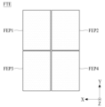
도 18을 도 15 내지 도 17과 결부하면, 본 예에 따른 전자 기기에서, 포스 터치 전극(FTE)은 복수의 포스 전극 패턴(FEP1, FEP2, FEP3, FEP4)을 포함한다.18 to 15 to 17, in the electronic device according to this example, the force touch electrode (FTE) includes a plurality of force electrode patterns (FEP1, FEP2, FEP3, FEP4).
상기 복수의 포스 전극 패턴(FEP1, FEP2, FEP3, FEP4) 각각은 하우징 플레이트(510)과 중첩되도록 디스플레이 패널(110), 즉 하부 기판(111)의 후면에 서로 분리되도록 격자 형태로 마련될 수 있다. 이에 따라, 복수의 포스 전극 패턴(FEP1, FEP2, FEP3, FEP4) 각각과 하우징 플레이트(510) 사이에는 복수의 정전 용량이 마련된다. 이때, 복수의 정전 용량 각각은 해당하는 포스 전극 패턴(FEP1, FEP2, FEP3, FEP4)과 하우징 플레이트(510) 사이의 거리 변화에 따라 변화된다. 이와 같은, 복수의 포스 전극 패턴(FEP1, FEP2, FEP3, FEP4) 각각은 터치 센싱 모드(TM)에서 멀티 포스 터치를 센싱하기 위해 사용된다.Each of the plurality of force electrode patterns (FEP1, FEP2, FEP3, and FEP4) may be provided in a grid form to be separated from each other on the back of the
상기 복수의 포스 전극 패턴(FEP1, FEP2, FEP3, FEP4) 각각은 복수의 포스 라우팅 라인을 통해서 구동 회로부(900), 즉 포스 터치 구동부(990)에 개별적으로 연결된다.Each of the plurality of force electrode patterns (FEP1, FEP2, FEP3, and FEP4) is individually connected to the
일 예에 따른 포스 터치 구동부(990)는, 도 16에 도시된 바와 같이, 호스트 제어부(910)로부터 공급되는 제 1 논리 상태의 모드 신호(MS)에 응답하여, 디스플레이 모드(DM) 동안 복수의 포스 전극 패턴(FEP1, FEP2, FEP3, FEP4) 각각을 전기적으로 하이 임피던스 상태로 전환한다. 이에 따라, 디스플레이 모드(DM) 동안 복수의 포스 전극 패턴(FEP1, FEP2, FEP3, FEP4) 각각은 전기적으로 하이 임피던스 상태, 즉 전기적으로 플로팅(floating)됨으로써 하우징(500)에 수납된 구동 회로부(900)에서 발생되는 정전기 또는 주파수 노이즈가 디스플레이 패널(110)의 내부로 유입되는 것을 차단하는 노이즈 차폐층의 역할을 한다.As shown in FIG. 16, the
그리고, 일 예에 따른 포스 터치 구동부(990)는, 도 16에 도시된 바와 같이, 호스트 제어부(910)로부터 공급되는 제 2 논리 상태의 모드 신호(MS)에 응답하여, 터치 센싱 모드(TM) 동안 복수의 포스 라우팅 라인을 통해서 복수의 포스 전극 패턴(FEP1, FEP2, FEP3, FEP4) 각각에 터치 구동 신호(TDS)를 인가한 후, 다시 복수의 포스 라우팅 라인을 통해서 복수의 포스 전극 패턴(FEP1, FEP2, FEP3, FEP4) 각각과 하우징(500) 사이의 정전 용량 변화를 센싱하여 복수의 포스 로우 데이터를 순차적으로 생성해 호스트 제어부(910)에 제공한다.And, as shown in FIG. 16, the
일 예에 따른 포스 터치 구동부(990)는 도 17에 도시된 호스트 제어부(910)로부터 공급되는 제 1 논리 상태의 모드 신호(MS)에 응답하여, 디스플레이 모드(DM) 동안 복수의 포스 라우팅 라인을 통해서 복수의 포스 전극 패턴(FEP1, FEP2, FEP3, FEP4) 각각을 전기적으로 하이 임피던스 상태, 즉 전기적으로 플로팅시킨다. 이에 따라, 디스플레이 모드(DM) 동안 복수의 포스 전극 패턴(FEP1, FEP2, FEP3, FEP4) 각각은 전기적으로 플로팅됨으로써 하우징(500)에 수납된 구동 회로부(900)에서 발생되는 정전기 또는 주파수 노이즈가 디스플레이 패널(110)의 내부로 유입되는 것을 차단하는 노이즈 차폐층의 역할을 한다.The
일 예에 따른 포스 터치 구동부(990)는, 도 17에 도시된 바와 같이, 호스트 제어부(910)로부터 공급되는 제 2 논리 상태의 모드 신호(MS)의 제 1 터치 센싱 구간(P1) 또는 터치 센싱 구간 신호(TSPS)에 따라 제 1 터치 센싱 구간(P1) 동안 복수의 포스 라우팅 라인을 통해서 복수의 포스 전극 패턴(FEP1, FEP2, FEP3, FEP4) 각각을 전기적으로 플로팅시킴으로써 하우징(500)에 수납된 구동 회로부(900)에서 발생되는 정전기 또는 주파수 노이즈가 터치 전극(TE)으로 유입되는 것을 차단한다.As shown in FIG. 17, the
그리고, 일 예에 따른 포스 터치 구동부(990)는, 도 17에 도시된 바와 같이, 호스트 제어부(910)로부터 공급되는 제 2 논리 상태의 모드 신호(MS)의 제 2 터치 센싱 구간(P2) 또는 포스 센싱 구간 신호(FSPS)에 따라 제 2 터치 센싱 구간(P2) 동안 복수의 포스 라우팅 라인을 통해서 복수의 포스 전극 패턴(FEP1, FEP2, FEP3, FEP4) 각각에 터치 구동 신호(TDS)를 공급한 후, 다시 복수의 포스 라우팅 라인을 통해서 복수의 포스 전극 패턴(FEP1, FEP2, FEP3, FEP4) 각각과 하우징(500) 사이의 정전 용량 변화를 센싱하여 복수의 포스 로우 데이터를 순차적으로 생성해 호스트 제어부(910)에 제공한다.And, as shown in FIG. 17, the
이와 같은, 본 예에 따른 전자 기기는 복수의 포스 전극 패턴(FEP1, FEP2, FEP3, FEP4) 각각을 통해 터치 포스를 개별적으로 센싱함으로써 멀티 포스 터치를 센싱할 수 있으며, 포스 터치의 위치와 위치별 터치 포스를 산출하고 이에 상응하는 다양한 어플리케이션을 실행할 수 있다. 특히, 본 예는 복수의 포스 전극 패턴(FEP1, FEP2, FEP3, FEP4) 각각에 대한 위치별 터치 포스를 세분화하여 포스 터치 기반의 보안 어플리케이션에 적용할 경우, 전자 기기의 보안성을 높일 수 있다. 여기서, 보안 어플리케이션은 전자 기기의 잠금 기능 또는 잠금 해제 기능을 수행하는 어플리케이션일 수 있다.As such, the electronic device according to the present example can sense multi-force touch by individually sensing the touch force through each of the plurality of force electrode patterns (FEP1, FEP2, FEP3, and FEP4), and the position of the force touch and each position. You can calculate touch force and run various applications corresponding to it. In particular, in this example, the security of electronic devices can be improved when applied to a force touch-based security application by subdividing the touch force by location for each of the plurality of force electrode patterns (FEP1, FEP2, FEP3, and FEP4). Here, the security application may be an application that performs a locking or unlocking function of an electronic device.
도 19는 도 1에 도시된 선 I-I' 및 선 II-II'의 다른 단면도로서, 이는 도 2에 도시된 전자 기기에 모듈 지지 부재를 추가로 구성한 것이다.FIG. 19 is another cross-sectional view taken along lines II-I' and II-II' shown in FIG. 1, in which a module support member is added to the electronic device shown in FIG. 2.
도 19를 도 1과 결부하면, 본 예에 따른 전자 기기의 모듈 지지 부재(250)는 디스플레이 모듈(100)의 후면 에지부와 하우징 플레이트(510)의 전면 에지부 사이에 일정한 높이를 가지도록 수직하게 마련되어 디스플레이 모듈(100)의 후면과 하우징 플레이트(510) 사이에 에어 갭(AG)을 마련한다. 즉, 상기 모듈 지지 부재(250)는 반사 시트(133)의 후면 에지부와 하우징 플레이트(510)의 전면 에지부 사이에 마련되어 하우징 플레이트(510)의 전면 에지부를 지지대로 하여 디스플레이 모듈(100)의 반사 시트(133)를 하우징 플레이트(510)의 전면으로부터 일정한 간격으로 이격시킴으로써 디스플레이 모듈(100)의 후면과 하우징 플레이트(510) 사이에 에어 갭(AG)을 마련한다.19 with FIG. 1, the
상기 에어 갭(AG)은 디스플레이 모듈(100)의 반사 시트(133)와 하우징 플레이트(510) 사이의 이격 공간으로 정의될 수 있다. 이러한, 에어 갭(AG)은 사용자의 터치 압력에 의해 디스플레이 모듈(100)이 상하 방향(Z)으로 유동될 수 있는 공간을 제공함으로써 사용자의 터치 압력에 따라 커버 윈도우(300)와 디스플레이 모듈(100)이 곡면 형태로 변형될 수 있도록 한다.The air gap AG may be defined as a space between the
일 예에 따른 모듈 지지 부재(250)는 탄성 복원력을 갖는 탄성 패드, 양면 부착성 폼 패드, 또는 스프링을 포함할 수 있다. 이러한 모듈 지지 부재(250)는 디스플레이 모듈(100)을 탄성 지지하면서 디스플레이 모듈(100)을 하우징 플레이트(510)에 부착시키는 역할도 함께 한다.The
추가적으로, 본 예에서, 커버 윈도우(300)는 투명 점착 부재에 의해 디스플레이 패널(110)의 전면 전체에 부착되지 않고 지지되면서 하우징(500)에 지지될 수 있다. 예를 들어, 커버 윈도우(300)는 하우징 측벽(530)의 홈부(550)에 배치된 탄성 부재(570)와 결합될 수 있다. 이에 따라, 커버 윈도우(300)는 디스플레이 모듈(100)과 하우징 측벽(530) 사이의 공간과 디스플레이 모듈(100)의 전면 전체를 덮음으로써 충격으로부터 디스플레이 모듈(100)을 보호하면서 디스플레이 모듈(100)과 하우징 측벽(530) 사이의 공간으로 이물질이 침투하는 것을 차단한다.Additionally, in this example, the
이와 같은, 본 예에 따른 전자 기기는 디스플레이 모듈(100)과 하우징 플레이트(510) 사이에 모듈 지지 부재(250)를 배치하여 디스플레이 모듈(100)과 하우징 플레이트(510) 사이에 에어 갭(AG)을 마련함으로써 상기 에어 갭(AG)을 마련하기 위해 디스플레이 모듈(100)을 커버 윈도우(300)에 부착시킬 필요가 없다. 이에 따라, 본 예는 도 2에 도시된 전자 기기와 같이, 광학 점착 부재(200)를 생략할 수 있다.As such, the electronic device according to this example arranges the
한편, 본 예에 따른 모듈 지지 부재(250)는 도 13 및 도 15 각각에 도시된 전자 기기의 디스플레이 모듈(100)과 하우징 플레이트(510) 사이에 마련되어 디스플레이 모듈(100)과 하우징 플레이트(510) 사이에 에어 갭(AG)을 마련할 수 있으며, 이 경우, 광학 점착 부재(200)는 생략되며, 커버 윈도우(300)는 디스플레이 패널(110)의 전면 전체에 부착되지 않고 지지되면서 하우징(500)에 지지될 수 있다.Meanwhile, the
도 20은 일 예에 따른 전자 기기를 나타내는 사시도이며, 도 21은 도 20에 도시된 선 III-III'의 단면도로서, 이는 디스플레이 모듈의 지지 구조를 변경한 것이다. 이에 따라, 이하에서는 디스플레이 모듈의 지지 구조와 관련된 구성들을 제외한 나머지 구성들은 도 1 내지 도 19와 동일하므로, 동일한 구성들에 대한 중복 설명은 생략하기로 한다.FIG. 20 is a perspective view showing an electronic device according to an example, and FIG. 21 is a cross-sectional view taken along line III-III' shown in FIG. 20, which shows a change in the support structure of the display module. Accordingly, hereinafter, the remaining configurations except for the configurations related to the support structure of the display module are the same as those in FIGS. 1 to 19, and thus duplicate descriptions of the same configurations will be omitted.
도 20 및 도 21을 참조하면, 일 예에 따른 전자 기기에서, 디스플레이 모듈(100)은 하우징(500)의 하우징 측벽(530)에 직접적으로 지지된다. 즉, 하우징 측벽(530)은 디스플레이 모듈(100), 보다 구체적으로, 디스플레이 패널(110)의 각 측면을 감싸지 않고 디스플레이 패널(110)의 후면 가장자리 부분을 지지한다. 하우징 측벽(530)의 최외곽 측면은 디스플레이 패널(110)의 최외곽 측면과 동일한 수직 선상(VL)에 위치할 수도 있고, 수직 선상(VL)보다 외부 방향으로 약간 돌출되어 위치할 수도 있고, 수직 선상(VL)보다 내부에 위치할 수도 있다. 따라서, 사용자(또는 시청자)가 위치한 디스플레이 패널(110)의 전방에서 바라볼 때, 하우징 측벽(530)은 디스플레이 패널(110)에 의해 거의 은폐될 수 있다.Referring to FIGS. 20 and 21 , in the electronic device according to one example, the
일 예에 따른 하우징 측벽(530)은 디스플레이 패널(110), 보다 구체적으로는 하부 편광 부재(115)의 후면 가장자리를 직접적으로 지지할 수 있다. 이 경우, 하부 편광 부재(115)는 디스플레이 패널(110)에 가해지는 충격을 완충하는 역할을 할 수 있다.The
일 예에 따른 하우징 측벽(530)은 하부 기판(111)의 후면 가장자리를 직접적으로 지지할 수 있으며, 이를 위해, 하부 편광 부재(115)의 가장자리는 제거될 수 있다. 이 경우, 본 예에 따른 전자 기기는 하부 편광 부재(115)만큼 슬림화될 수 있다.The
상기 하우징 측벽(530)은 지지 부재(580)를 통해서 디스플레이 패널(110)의 후면 가장자리 부분을 지지할 수도 있다. 일 예에 따른 지지 부재(580)는 탄성 복원력을 갖는 탄성 패드 또는 양면 부착성 폼 패드를 포함할 수 있다. 이러한 지지 부재(580)는 디스플레이 패널(110)과 하우징 측벽(530) 간의 직접적인 접촉을 방지하면서 디스플레이 패널(110)과 하우징 측벽(530) 사이의 공간으로 이물질이 침투하는 것을 차단할 수 있다.The
선택적으로, 본 예에 디스플레이 모듈(100)은 디스플레이 패널(110)의 각 외측면을 덮는 측면 실링 부재(170)를 더 포함한다.Optionally, the
상기 측면 실링 부재(170)는 하부 편광 부재(115)과 하부 기판(111) 및 상부 기판(113) 각각의 최외곽 측면을 덮도록 마련된다. 이러한 측면 실링 부재(170)는 디스플레이 패널(110)의 측면 빛샘, 즉 상부 기판(113) 내에서 최외곽 측면으로 진행하는 광에 의해 측면 빛샘을 방지하는 역할을 한다.The
상기 측면 실링 부재(170)는 실리콘 계열 또는 자외선(UV) 경화 계열의 실링제(또는 수지(Resin))로 이루어질 수 있으나, 공정 택 타임(Tack Time)을 고려하면 자외선(UV) 경화 계열의 실링제로 이루어지는 것이 바람직하다. 또한, 상기 측면 실링 부재(170)는 유색(예를 들어, 청색, 적색, 청록색, 또는 흑색)이 될 수 있으나, 이에 한정되지 않고, 측면 빛샘을 방지하기 위한 유색 수지 또는 광 차단 수지로 이루어지는 것이 바람직하다.The
상기 측면 실링 부재(170)의 상면 일부는 상부 편광 부재(117)에 의해 덮일 수 있다. 이를 위해, 상부 편광 부재(117)는 측면 실링 부재(170)의 전면(前面) 일부를 덮도록 연장되어 측면 실링 부재(170)의 전면(前面) 일부에 부착된 연장부(117a)를 포함한다. 이에 따라, 측면 실링 부재(170)와 디스플레이 패널(110) 사이의 접합면은 상부 편광 부재(117)의 연장부(117a)에 의해 은폐될 수 있다.A portion of the upper surface of the
추가적으로, 측면 실링 부재(170)는 하부 편광 부재(115)과 하부 기판(111) 및 상부 기판(113) 각각의 최외곽 측면뿐만 아니라 상부 편광 부재(117) 및 커버 윈도우(300)의 각 측면을 덮도록 마련될 수도 있다. 이 경우, 측면 실링 부재(170)는 커버 윈도우(300) 내에서 최외곽 측면으로 진행하는 측면 빛샘을 방지하는 역할을 한다.Additionally, the
이와 같은, 본 예는 하우징 측벽(530)을 통해 디스플레이 패널(110)의 후면을 지지함으로써 하우징 측벽(530)에 의한 전자 기기의 베젤 폭을 제거할 수 있으며, 이를 통해 제로 베젤 디스플레이를 제공할 수 있다.In this example, by supporting the rear of the
도 22는 일 예에 따른 전자 기기를 나타내는 사시도이며, 도 23은 도 22에 도시된 선 IV-IV'의 단면도로서, 이는 하우징의 전기적 연결 구조를 설명하기 위한 것이다. 이에 따라, 이하에서는 하우징의 전기적 연결 구조와 관련된 구성들을 제외한 나머지 구성들은 도 1 내지 도 21과 동일하므로, 동일한 구성들에 대한 중복 설명은 생략하기로 한다.FIG. 22 is a perspective view showing an electronic device according to an example, and FIG. 23 is a cross-sectional view taken along line IV-IV' shown in FIG. 22, which is for explaining the electrical connection structure of the housing. Accordingly, in the following, the remaining configurations except for the configurations related to the electrical connection structure of the housing are the same as those in FIGS. 1 to 21, so duplicate descriptions of the same configurations will be omitted.
도 22 및 도 23을 참조하면, 일 예에 따른 전자 기기는 인쇄 회로 기판(980), 전원 공급 회로(990), 플렉서블 회로 필름(991), 및 도전성 연결 부재(993)을 더 포함한다.Referring to FIGS. 22 and 23 , the electronic device according to one example further includes a printed
상기 인쇄 회로 기판(980)은 하우징(500)의 시스템 수납 공간(500s)에 수납되어 전원 공급 회로(990)를 지지하며, 전술한 본 예에 따른 구동 회로부(900)를 지지한다.The printed
상기 전원 공급 회로(990)는 외부 전원 또는 배터리로부터 공급되는 입력 전원을 이용하여 접지 전압과 디스플레이 패널(110)에 영상을 표시하기 위해 필요한 직류 전압 및 교류 전압을 포함하는 구동 전압을 생성하여 출력한다.The
상기 플렉서블 회로 필름(991)은 디스플레이 패널(110)의 하부 기판(111)에 마련된 패드부(PP)와 인쇄 회로 기판(980)을 연결한다. 이러한 플렉서블 회로 필름(991)의 일단은 하우징 플레이트(510)에 마련된 필름 관통 홀(500h)을 통과하여 패드부(PP)에 전기적으로 연결된다. 그리고, 플렉서블 회로 필름(991)의 타단은 인쇄 회로 기판(980)에 전기적으로 연결한다. 이러한 플렉서블 회로 필름(991)은 구동 회로부(900)에서 출력되는 신호를 패드부(PP)를 통해 하부 기판(111)에 마련된 신호 라인에 공급한다.The
선택적으로, 구동 회로부(900)에 포함된 패널 구동부(970)는 플렉서블 회로 필름(991)에 실장되어 패드부(PP)를 통해서 하부 기판(111)에 마련된 신호 라인과 전기적으로 연결될 수도 있다. 또한, 패널 구동부(970)는 하부 기판(111)에 마련된 회로 실장 영역에 배치되어 패드부(PP)와 전기적으로 연결됨과 아울러 하부 기판(111)에 마련된 신호 라인과 전기적으로 연결될 수도 있다.Optionally, the
상기 도전성 연결 부재(993)는 전원 공급 회로(990)로부터 공급되는 접지 전압 또는 일정한 전압 레벨을 갖는 직류 또는 교류 전압을 하우징(500)에 공급함으로써 하우징(500)이 전기적으로 접지(GND)되거나 일정한 전압 레벨로 유지되도록 한다.The
일 예에 따른 도전성 연결 부재(993)는 하우징 측벽(530)과 나란한 플렉서블 회로 필름(991)에 마련된 전원 패드(991a)와 하우징 측벽(530)을 전기적으로 연결한다. 도전성 연결 부재(993)의 일측은 플렉서블 회로 필름(991)에 마련된 전원 패드(991a)에 전기적으로 연결되고, 도전성 연결 부재(993)의 타측은 하우징 측벽(530)의 내측벽에 전기적으로 연결된다. 이때, 도전성 연결 부재(993)는 전도성 접착제를 매개로 하여 전원 패드(991a)와 하우징 측벽(530) 각각과 전기적으로 연결될 수 있다. 따라서, 도전성 연결 부재(993)는 전원 공급 회로(900)로부터 전원 패드(991a)에 공급되는 접지 전압 또는 일정한 전압 레벨을 갖는 직류 또는 교류 전압을 하우징 측벽(530)에 인가한다. 이 경우, 도전성 연결 부재(993)는 도전성 와이어, 도전성 테이프, 또는 도전성 페이스트 등이 될 수 있다.The
일 예에 따른 도전성 연결 부재(993)는 플렉서블 회로 필름(991)에 마련된 전원 패드(991a)와 하우징 측벽(530)을 전기적으로 연결하지 않고, 인쇄 회로 기판(980)에 마련된 전원 패드(981)와 하우징 플레이트(510)을 전기적으로 연결할 수도 있다. 즉, 도전성 연결 부재(993)의 일측은 하우징 플레이트(510)와 마주하는 인쇄 회로 기판(980)의 제 1 면 또는 제 1 면과 반대되는 제 2 면에 마련된 전원 패드(981)에 전기적으로 연결되고, 도전성 연결 부재(993)의 타측은 인쇄 회로 기판(980)과 마주하는 하우징 플레이트(510)의 후면에 전기적으로 연결된다. 이때, 도전성 연결 부재(993)는 전도성 접착제를 매개로 하여 전원 패드(991a)와 하우징 플레이트(510)의 후면 각각과 전기적으로 연결될 수 있다. 따라서, 도전성 연결 부재(993)는 전원 공급 회로(900)로부터 전원 패드(991a)에 공급되는 접지 전압 또는 일정한 전압 레벨을 갖는 직류 또는 교류 전압을 하우징 플레이트(510)에 인가한다. 이 경우, 도전성 연결 부재(993)는 도전성 와이어 또는 도전성 테이프 등이 될 수 있다.The
이와 같은, 본 예는 도전성 연결 부재(993)를 통해서 하우징(500)에 접지 전원 또는 일정한 전압 레벨을 갖는 직류 또는 교류 전압을 공급함으로써 하우징(500)에 공급되는 전압을 기반으로 하우징 플레이트(510)와 터치 전극(TE) 간의 거리 변화에 따른 정전 용량 변화를 용이하게 센싱할 수 있다.In this example, the
부가적으로, 도 1에는 일 예에 따른 전자 기기로서 스마트 폰(smart phone)이 도시되었지만, 이에 한정되지 않고, 본 발명의 예는 자기 정전 용량 방식의 인-셀 터치 패널을 포함하는 디스플레이 모듈과 디스플레이 모듈을 수납하는 금속 재질의 하우징을 포함하는 모든 전자 기기에 동일하게 적용될 수 있다. 여기서, 전자 기기는 전자 수첩, 전자 책, PMP(Portable Multimedia Player), 네비게이션, UMPC(Ultra Mobile PC), 모바일 폰, 태블릿 PC(Personal Computer), 스마트 와치(smart watch), 와치 폰(watch phone), 웨어러블 기기(Wearable device), 및 이동 통신 단말기 등과 같은 휴대용 전자 기기, 텔레비전, 노트북, 모니터, 카메라, 캠코더, 또는 디스플레이를 갖는 가전 기기 등이 될 수 있다. 또한, 본 예에 따른 전자 기기는 액정층을 갖는 디스플레이 패널 이외에 유기 발광 소자를 갖는 인-셀 터치 패널을 포함하는 유기 발광 디스플레이 모듈과 디스플레이 모듈을 수납하는 금속 재질의 하우징을 포함하는 유기 발광 표시 장치에도 동일하게 적용될 수 있다.Additionally, in FIG. 1, a smart phone is shown as an electronic device according to an example, but it is not limited thereto, and an example of the present invention includes a display module including a self-capacitance in-cell touch panel and It can be equally applied to all electronic devices that include a metal housing that stores a display module. Here, the electronic devices include electronic notebooks, e-books, PMPs (Portable Multimedia Players), navigation, UMPCs (Ultra Mobile PCs), mobile phones, tablet PCs (Personal Computers), smart watches, and watch phones. , wearable devices, and portable electronic devices such as mobile communication terminals, televisions, laptops, monitors, cameras, camcorders, or home appliances with displays. In addition, the electronic device according to the present example includes an organic light emitting display module including an in-cell touch panel having an organic light emitting element in addition to a display panel having a liquid crystal layer, and an organic light emitting display device including a housing made of metal for storing the display module. The same can be applied to .
이상에서 설명한 본 발명은 전술한 실시 예 및 첨부된 도면에 한정되는 것이 아니고, 본 발명의 기술적 사항을 벗어나지 않는 범위 내에서 여러 가지 치환, 변형 및 변경이 가능하다는 것이 본 발명이 속하는 기술 분야에서 통상의 지식을 가진 자에게 있어 명백할 것이다. 그러므로, 본 발명의 범위는 후술하는 특허청구범위에 의하여 나타내어지며, 특허청구범위의 의미 및 범위 그리고 그 등가 개념으로부터 도출되는 모든 변경 또는 변형된 형태가 본 발명의 범위에 포함되는 것으로 해석되어야 한다.The present invention described above is not limited to the above-described embodiments and the accompanying drawings, and it is commonly known in the technical field to which the present invention pertains that various substitutions, modifications, and changes can be made without departing from the technical details of the present invention. It will be clear to those who have the knowledge of. Therefore, the scope of the present invention is indicated by the claims described later, and all changes or modified forms derived from the meaning and scope of the claims and their equivalent concepts should be interpreted as being included in the scope of the present invention.
100: 디스플레이 모듈 110: 디스플레이 패널
111: 하부 기판 119: 투명 전도층
200: 투명 점착 부재 250: 모듈 지지 부재
300: 커버 윈도우 500: 하우징
510: 하우징 플레이트 530: 하우징 측벽
600: 후면 커버 700: 완충 부재
900: 구동 회로부 910: 호스트 제어부
930: 터치 구동부 950: 로드 프리 신호 생성부
970: 패널 구동부 990: 포스 터치 구동부
100: display module 110: display panel
111: lower substrate 119: transparent conductive layer
200: Transparent adhesive member 250: Module support member
300: cover window 500: housing
510: housing plate 530: housing side wall
600: Rear cover 700: Shock absorbing member
900: Driving circuit unit 910: Host control unit
930: Touch driving unit 950: Load-free signal generating unit
970: Panel driving unit 990: Force touch driving unit
Claims (22)
상기 디스플레이 모듈의 전면(前面)을 덮는 커버 윈도우;
전기적인 전도성을 가지면서 상기 디스플레이 모듈의 후면 아래에 배치된 하우징 플레이트 및 상기 디스플레이 모듈의 측면의 적어도 일부를 감싸거나 상기 디스플레이 모듈을 지지하는 하우징 측벽을 갖는 하우징; 및
하나 이상의 터치 전극과 상기 하우징 플레이트 사이의 거리 변화에 따라 상기 하나 이상의 터치 전극과 상기 하우징 플레이트 사이의 정전 용량 변화를 센싱하는 구동 회로부를 포함하고,
상기 구동 회로부는,
터치 센싱 모드의 제 1 터치 센싱 기간 동안 상기 하나 이상의 터치 전극에 터치 구동 신호를 공급하고 상기 하나 이상의 터치 전극의 정전 용량 변화를 센싱하여 터치 로우 데이터를 생성하는 터치 구동부;
터치 센싱 모드의 제 2 터치 센싱 기간 동안 상기 투명 전도층에 포스 터치 구동 신호를 공급하고 상기 투명 전도층과 상기 하우징 플레이트 사이의 정전 용량 변화를 센싱하여 포스 터치 로우 데이터를 생성하는 포스 터치 구동부; 및
상기 터치 로우 데이터를 기반으로 터치 위치를 산출하고 상기 포스 터치 로우 데이터를 기반으로 터치 포스 레벨을 산출하는 호스트 제어부를 갖는, 전자 기기.A display module having a plurality of touch electrodes disposed between an upper substrate and a lower substrate, and a transparent conductive layer disposed on the back of the lower substrate;
a cover window covering the front of the display module;
a housing that is electrically conductive and has a housing plate disposed below the rear of the display module and a housing side wall that surrounds at least a portion of a side of the display module or supports the display module; and
A driving circuit unit that senses a change in capacitance between the one or more touch electrodes and the housing plate according to a change in the distance between the one or more touch electrodes and the housing plate,
The driving circuit unit,
a touch driver that supplies a touch driving signal to the one or more touch electrodes and generates touch raw data by sensing a change in capacitance of the one or more touch electrodes during a first touch sensing period of the touch sensing mode;
A force touch driver that supplies a force touch driving signal to the transparent conductive layer and senses a change in capacitance between the transparent conductive layer and the housing plate to generate force touch raw data during the second touch sensing period of the touch sensing mode; and
An electronic device having a host control unit that calculates a touch position based on the touch raw data and a touch force level based on the force touch raw data.
상기 디스플레이 모듈은,
게이트 라인과 데이터 라인 및 디스플레이 모드 동안 공통 전극으로 사용되는 상기 터치 전극을 포함하는 상기 하부 기판;
상기 하부 기판과 합착된 상기 상부 기판; 및
상기 하부 기판과 상기 상부 기판 사이의 액정층을 포함하는, 전자 기기.According to claim 1,
The display module is,
the lower substrate including a gate line, a data line, and the touch electrode used as a common electrode during a display mode;
The upper substrate bonded to the lower substrate; and
An electronic device comprising a liquid crystal layer between the lower substrate and the upper substrate.
상기 투명 전도층은 전기적으로 플로팅된, 전자 기기.According to claim 1,
The electronic device of claim 1, wherein the transparent conductive layer is electrically floating.
디스플레이 모드 동안, 상기 터치 전극에는 공통 전압이 공급되고, 상기 투명 전도층은 전기적으로 플로팅되는, 전자 기기.According to claim 1,
During the display mode, the touch electrode is supplied with a common voltage and the transparent conductive layer is electrically floating.
디스플레이 모드 동안 상기 터치 전극에는 공통 전압이 공급되고, 상기 제 2 터치 센싱 구간 동안 상기 터치 전극은 전기적으로 플로팅되며,
상기 투명 전도층은 상기 디스플레이 모드 동안 전기적으로 플로팅되고, 상기 제 1 터치 센싱 기간 동안 전기적으로 플로팅되는, 전자 기기.According to claim 1,
A common voltage is supplied to the touch electrode during the display mode, and the touch electrode is electrically floating during the second touch sensing period,
wherein the transparent conductive layer is electrically floating during the display mode and electrically floating during the first touch sensing period.
상기 디스플레이 모듈의 후면으로부터 이격되도록 상기 하우징 플레이트 상에 배치되고, 상기 디스플레이 모듈의 후면 에지부를 제외한 나머지 부분과 중첩되는 완충 부재를 더 포함하는, 전자 기기.According to claim 1,
The electronic device further includes a buffer member disposed on the housing plate to be spaced from the rear of the display module and overlapping with the remaining portion except for the rear edge of the display module.
상기 완충부재는 상기 디스플레이 모듈의 중앙부를 중심으로 하는 원 형태의 단면을 갖는, 전자 기기.According to clause 9,
The electronic device wherein the buffer member has a circular cross-section centered on the central part of the display module.
상기 완충 부재는 상기 디스플레이 모듈의 중앙부를 중심으로 하는 사각 형태의 단면을 갖는, 전자 기기.According to clause 9,
The electronic device wherein the buffer member has a square cross-section centered on the central portion of the display module.
상기 사각 형태의 단면을 갖는 상기 완충 부재의 하나 이상의 모서리 부분은 라운드되는, 전자 기기.According to claim 11,
An electronic device, wherein at least one corner of the cushioning member having a square cross-section is rounded.
상기 완충 부재는 PU(polyurethane) 재질을 포함하는, 전자 기기.According to clause 9,
The electronic device wherein the cushioning member includes a PU (polyurethane) material.
상기 하우징 측벽은 내부면에 마련된 홈부, 및 상기 홈부의 바닥면과 상기 커버 윈도우의 후면 가장자리 사이에 배치된 탄성 부재를 포함하고,
상기 커버 윈도우는 상기 디스플레이 모듈의 전면(前面) 전체 및 상기 디스플레이 모듈과 상기 하우징 측벽 사이의 공간을 덮는, 전자 기기.According to claim 1,
The housing side wall includes a groove provided on the inner surface, and an elastic member disposed between the bottom surface of the groove and the rear edge of the cover window,
The cover window covers the entire front of the display module and the space between the display module and the side wall of the housing.
상기 디스플레이 모듈과 상기 하우징 측벽 사이의 지지 부재를 더 포함하고,
상기 하우징 측벽은 상기 지지 부재를 매개로 하여 상기 디스플레이 모듈의 후면 가장자리를 지지하는, 전자 기기.According to claim 1,
Further comprising a support member between the display module and the housing sidewall,
The housing side wall supports the rear edge of the display module via the support member.
상기 지지 부재는 탄성 패드 또는 접착 폼 패드를 포함하는, 전자 기기.According to claim 15,
The electronic device, wherein the support member includes an elastic pad or an adhesive foam pad.
상기 디스플레이 모듈의 외측면을 덮는 측면 실링 부재를 더 포함하는, 전자 기기.According to claim 1,
An electronic device further comprising a side sealing member covering an outer surface of the display module.
상기 측면 실링 부재는 자외선(UV) 경화성 실런트를 포함하는, 전자 기기.According to claim 17,
The electronic device, wherein the side sealing member includes an ultraviolet (UV) curable sealant.
상기 디스플레이 모듈의 적어도 일부는 상기 측면 실링 부재의 전면(前面)을 덮는, 전자 기기.According to claim 17,
At least a portion of the display module covers a front surface of the side sealing member.
상기 디스플레이 모듈의 후면 가장자리와 상기 하우징 플레이트의 전면(前面) 가장자리 사이에 수직하게 마련되고 상기 디스플레이 모듈의 후면과 상기 하우징 플레이트 사이에 에어 갭을 마련하는 모듈 지지 부재를 더 포함하는, 전자 기기.According to claim 1,
The electronic device further includes a module support member provided vertically between the rear edge of the display module and the front edge of the housing plate and providing an air gap between the rear edge of the display module and the housing plate.
상기 하우징 플레이트 아래에 배치되고 구동 회로부가 실장된 인쇄 회로 기판; 및
상기 디스플레이 모듈과 상기 인쇄 회로 기판을 전기적으로 연결하는 플렉서블 회로 필름을 더 포함하고,
상기 플렉서블 회로 필름은 상기 인쇄 회로 기판으로부터 상기 하우징 플레이트에 마련된 필름 관통 홀을 통과하여 상기 디스플레이 모듈의 일부로 연장된, 전자 기기.According to claim 1,
a printed circuit board disposed below the housing plate and on which a driving circuit unit is mounted; and
Further comprising a flexible circuit film electrically connecting the display module and the printed circuit board,
The flexible circuit film extends from the printed circuit board through a film through-hole provided in the housing plate to a part of the display module.
상기 하우징 플레이트를 상기 인쇄 회로 기판에 전기적으로 연결하는 전도성 연결 부재를 더 포함하며,
상기 하우징 플레이트는 상기 전도성 연결 부재를 통해 접지된, 전자 기기.
According to claim 21,
Further comprising a conductive connection member electrically connecting the housing plate to the printed circuit board,
The electronic device of claim 1, wherein the housing plate is grounded through the conductive connection member.
Priority Applications (3)
| Application Number | Priority Date | Filing Date | Title |
|---|---|---|---|
| US15/394,692 US10209819B2 (en) | 2015-12-31 | 2016-12-29 | Electronic device |
| CN201611245299.2A CN107015693B (en) | 2015-12-31 | 2016-12-29 | Electronic device |
| DE102016125907.1A DE102016125907A1 (en) | 2015-12-31 | 2016-12-30 | Electronic device |
Applications Claiming Priority (2)
| Application Number | Priority Date | Filing Date | Title |
|---|---|---|---|
| KR20150191783 | 2015-12-31 | ||
| KR1020150191783 | 2015-12-31 |
Publications (2)
| Publication Number | Publication Date |
|---|---|
| KR20170080482A KR20170080482A (en) | 2017-07-10 |
| KR102668555B1 true KR102668555B1 (en) | 2024-05-23 |
Family
ID=59356075
Family Applications (1)
| Application Number | Title | Priority Date | Filing Date |
|---|---|---|---|
| KR1020160176017A Active KR102668555B1 (en) | 2015-12-31 | 2016-12-21 | Electronic device |
Country Status (2)
| Country | Link |
|---|---|
| KR (1) | KR102668555B1 (en) |
| CN (1) | CN107015693B (en) |
Families Citing this family (8)
| Publication number | Priority date | Publication date | Assignee | Title |
|---|---|---|---|---|
| KR102382639B1 (en) | 2017-10-31 | 2022-04-05 | 엘지디스플레이 주식회사 | Display device with touch sensor and manufacturing method for the same |
| KR102567559B1 (en) * | 2017-11-21 | 2023-08-14 | 엘지디스플레이 주식회사 | Electronic apparatus |
| CN107957814B (en) * | 2017-12-13 | 2020-12-29 | 业成科技(成都)有限公司 | Touch display device and touch module thereof |
| CN108664163A (en) * | 2018-04-26 | 2018-10-16 | 北京集创北方科技股份有限公司 | Control method and touch display system |
| CN108803929A (en) * | 2018-06-05 | 2018-11-13 | 北京小米移动软件有限公司 | Pressure touch screen, pressure touch method and electronic equipment |
| KR102589247B1 (en) * | 2018-12-20 | 2023-10-12 | 엘지디스플레이 주식회사 | Display apparatus |
| KR102703646B1 (en) * | 2018-12-28 | 2024-09-06 | 엘지디스플레이 주식회사 | Display device having a touch panel disposed between a display panel and a cover window |
| TWI809636B (en) * | 2021-12-30 | 2023-07-21 | 財團法人工業技術研究院 | Pixel structure |
Citations (1)
| Publication number | Priority date | Publication date | Assignee | Title |
|---|---|---|---|---|
| KR101565822B1 (en) * | 2015-06-22 | 2015-11-04 | 주식회사 하이딥 | Smartphone |
Family Cites Families (7)
| Publication number | Priority date | Publication date | Assignee | Title |
|---|---|---|---|---|
| KR20090112118A (en) * | 2008-04-23 | 2009-10-28 | 엘지이노텍 주식회사 | Display |
| JP5493739B2 (en) * | 2009-03-19 | 2014-05-14 | ソニー株式会社 | Sensor device and information processing device |
| CN103988156B (en) * | 2011-12-08 | 2017-10-31 | 索尼移动通信株式会社 | Input interface, portable electric device and the method for manufacturing input interface |
| US9459738B2 (en) * | 2012-03-06 | 2016-10-04 | Apple Inc. | Calibration for pressure effects on touch sensor panels |
| KR101855027B1 (en) * | 2014-02-12 | 2018-05-04 | 애플 인크. | Force determination employing sheet sensor and capacitive array |
| US9671915B2 (en) * | 2015-06-30 | 2017-06-06 | Synaptics Incorporated | Avoidance of bending effects in a touch sensor device |
| CN105183230B (en) * | 2015-09-18 | 2017-09-19 | 京东方科技集团股份有限公司 | Display device, pressure detection method and pressure detection device |
-
2016
- 2016-12-21 KR KR1020160176017A patent/KR102668555B1/en active Active
- 2016-12-29 CN CN201611245299.2A patent/CN107015693B/en active Active
Patent Citations (1)
| Publication number | Priority date | Publication date | Assignee | Title |
|---|---|---|---|---|
| KR101565822B1 (en) * | 2015-06-22 | 2015-11-04 | 주식회사 하이딥 | Smartphone |
Also Published As
| Publication number | Publication date |
|---|---|
| CN107015693A (en) | 2017-08-04 |
| CN107015693B (en) | 2019-12-03 |
| KR20170080482A (en) | 2017-07-10 |
Similar Documents
| Publication | Publication Date | Title |
|---|---|---|
| US10209819B2 (en) | Electronic device | |
| KR102668555B1 (en) | Electronic device | |
| CN106557196B (en) | Electronic device with pressure touch function | |
| KR102657011B1 (en) | Touch display device and its driving method | |
| KR102747669B1 (en) | Display device | |
| US9569030B2 (en) | Touch screen display device with in-set signals, driver circuit for the touch screen display device, and method for driving the touch screen display device | |
| KR102518377B1 (en) | Finger sensor integrated type touch screen device | |
| EP3040828B1 (en) | Touch panel and display device including the same | |
| CN106125997B (en) | Force sensor substrate | |
| KR102045809B1 (en) | Touch sensor integrated type display device | |
| US20110267305A1 (en) | Integrated capacitive sensing and displaying | |
| KR20170010935A (en) | Finger sensor integrated type touch screen device | |
| US9594458B2 (en) | Shielding with display elements | |
| CN114647330A (en) | Electronic device and driving method thereof | |
| KR102504495B1 (en) | Touch sensor integrated type display device | |
| US20120229420A1 (en) | Mems display with touch control function | |
| EP3226112B1 (en) | Touch display device | |
| KR102395112B1 (en) | Touch panel and electronic device comprisong the same | |
| CN205229993U (en) | Display device | |
| KR102082684B1 (en) | Touch panel and display device using the same | |
| KR102483875B1 (en) | Electronic device and method for touch sensing the same | |
| KR102685938B1 (en) | Display apparatus and electronic device comprising the same | |
| KR20170062646A (en) | Touch screen panel and display device comprising the same | |
| KR102371166B1 (en) | Display device |
Legal Events
| Date | Code | Title | Description |
|---|---|---|---|
| PA0109 | Patent application |
Patent event code: PA01091R01D Comment text: Patent Application Patent event date: 20161221 |
|
| PG1501 | Laying open of application | ||
| A201 | Request for examination | ||
| PA0201 | Request for examination |
Patent event code: PA02012R01D Patent event date: 20211123 Comment text: Request for Examination of Application Patent event code: PA02011R01I Patent event date: 20161221 Comment text: Patent Application |
|
| E902 | Notification of reason for refusal | ||
| PE0902 | Notice of grounds for rejection |
Comment text: Notification of reason for refusal Patent event date: 20231016 Patent event code: PE09021S01D |
|
| E701 | Decision to grant or registration of patent right | ||
| PE0701 | Decision of registration |
Patent event code: PE07011S01D Comment text: Decision to Grant Registration Patent event date: 20240424 |
|
| GRNT | Written decision to grant | ||
| PR0701 | Registration of establishment |
Comment text: Registration of Establishment Patent event date: 20240520 Patent event code: PR07011E01D |
|
| PR1002 | Payment of registration fee |
Payment date: 20240520 End annual number: 3 Start annual number: 1 |
|
| PG1601 | Publication of registration |