KR102633028B1 - Semiconductor device and display device having thereof - Google Patents
Semiconductor device and display device having thereof Download PDFInfo
- Publication number
- KR102633028B1 KR102633028B1 KR1020170016228A KR20170016228A KR102633028B1 KR 102633028 B1 KR102633028 B1 KR 102633028B1 KR 1020170016228 A KR1020170016228 A KR 1020170016228A KR 20170016228 A KR20170016228 A KR 20170016228A KR 102633028 B1 KR102633028 B1 KR 102633028B1
- Authority
- KR
- South Korea
- Prior art keywords
- layer
- semiconductor layer
- substrate
- disposed
- conductivity type
- Prior art date
- Legal status (The legal status is an assumption and is not a legal conclusion. Google has not performed a legal analysis and makes no representation as to the accuracy of the status listed.)
- Active
Links
Images


Classifications
-
- H01L33/02—
-
- H—ELECTRICITY
- H10—SEMICONDUCTOR DEVICES; ELECTRIC SOLID-STATE DEVICES NOT OTHERWISE PROVIDED FOR
- H10H—INORGANIC LIGHT-EMITTING SEMICONDUCTOR DEVICES HAVING POTENTIAL BARRIERS
- H10H20/00—Individual inorganic light-emitting semiconductor devices having potential barriers, e.g. light-emitting diodes [LED]
- H10H20/80—Constructional details
- H10H20/81—Bodies
-
- H01L33/005—
-
- H01L33/06—
-
- H01L33/36—
-
- H—ELECTRICITY
- H05—ELECTRIC TECHNIQUES NOT OTHERWISE PROVIDED FOR
- H05B—ELECTRIC HEATING; ELECTRIC LIGHT SOURCES NOT OTHERWISE PROVIDED FOR; CIRCUIT ARRANGEMENTS FOR ELECTRIC LIGHT SOURCES, IN GENERAL
- H05B33/00—Electroluminescent light sources
- H05B33/12—Light sources with substantially two-dimensional radiating surfaces
-
- H—ELECTRICITY
- H10—SEMICONDUCTOR DEVICES; ELECTRIC SOLID-STATE DEVICES NOT OTHERWISE PROVIDED FOR
- H10H—INORGANIC LIGHT-EMITTING SEMICONDUCTOR DEVICES HAVING POTENTIAL BARRIERS
- H10H20/00—Individual inorganic light-emitting semiconductor devices having potential barriers, e.g. light-emitting diodes [LED]
- H10H20/01—Manufacture or treatment
-
- H—ELECTRICITY
- H10—SEMICONDUCTOR DEVICES; ELECTRIC SOLID-STATE DEVICES NOT OTHERWISE PROVIDED FOR
- H10H—INORGANIC LIGHT-EMITTING SEMICONDUCTOR DEVICES HAVING POTENTIAL BARRIERS
- H10H20/00—Individual inorganic light-emitting semiconductor devices having potential barriers, e.g. light-emitting diodes [LED]
- H10H20/80—Constructional details
- H10H20/81—Bodies
- H10H20/811—Bodies having quantum effect structures or superlattices, e.g. tunnel junctions
- H10H20/812—Bodies having quantum effect structures or superlattices, e.g. tunnel junctions within the light-emitting regions, e.g. having quantum confinement structures
-
- H—ELECTRICITY
- H10—SEMICONDUCTOR DEVICES; ELECTRIC SOLID-STATE DEVICES NOT OTHERWISE PROVIDED FOR
- H10H—INORGANIC LIGHT-EMITTING SEMICONDUCTOR DEVICES HAVING POTENTIAL BARRIERS
- H10H20/00—Individual inorganic light-emitting semiconductor devices having potential barriers, e.g. light-emitting diodes [LED]
- H10H20/80—Constructional details
- H10H20/83—Electrodes
-
- H—ELECTRICITY
- H01—ELECTRIC ELEMENTS
- H01L—SEMICONDUCTOR DEVICES NOT COVERED BY CLASS H10
- H01L2924/00—Indexing scheme for arrangements or methods for connecting or disconnecting semiconductor or solid-state bodies as covered by H01L24/00
- H01L2924/10—Details of semiconductor or other solid state devices to be connected
- H01L2924/11—Device type
- H01L2924/12—Passive devices, e.g. 2 terminal devices
- H01L2924/1204—Optical Diode
- H01L2924/12041—LED
Landscapes
- Led Devices (AREA)
Abstract
실시 예는, 기판; 상기 기판 상에 배치되는 결합층; 제1 도전형 반도체층, 제2 도전형 반도체층 및 상기 제1 도전형 반도체층과 상기 제2 도전형 반도체층 사이에 배치되는 활성층을 포함하고 상기 결합층 상에 배치되는 발광구조물; 상기 제1 도전형 반도체층과 연결되는 제1 전극; 상기 제2 도전형 반도체층과 연결되는 제2 전극; 및 상기 결합층 및 상기 발광구조물을 덮는 보호층;을 포함하는 반도체 소자를 개시한다.Examples include: a substrate; a bonding layer disposed on the substrate; A light emitting structure comprising a first conductive semiconductor layer, a second conductive semiconductor layer, and an active layer disposed between the first conductive semiconductor layer and the second conductive semiconductor layer, and disposed on the bonding layer; a first electrode connected to the first conductive semiconductor layer; a second electrode connected to the second conductive semiconductor layer; and a protective layer covering the bonding layer and the light emitting structure.
Description
실시 예는 반도체 소자 및 이를 포함하는 디스플레이 장치에 관한 것이다.The embodiment relates to a semiconductor device and a display device including the same.
발광 다이오드(Light Emitting Diode: LED)는 전류가 인가되면 광을 방출하는 발광 소자 중 하나이다. 발광 다이오드는 저 전압으로 고효율의 광을 방출할 수 있어 에너지 절감 효과가 뛰어나다. 최근, 발광 다이오드의 휘도 문제가 크게 개선되어, 액정표시장치의 백라이트 유닛(Backlight Unit), 전광판, 표시기, 가전 제품 등과 같은 각종 기기에 적용되고 있다.Light Emitting Diode (LED) is one of the light emitting devices that emits light when current is applied. Light-emitting diodes can emit high-efficiency light at low voltage, providing excellent energy savings. Recently, the luminance problem of light emitting diodes has been greatly improved, and they are being applied to various devices such as backlight units of liquid crystal displays, electronic signs, indicators, and home appliances.
AlGaInP를 갖는 발광 다이오드는 GaAs 기판을 성장기판으로 사용하나, 반도체 칩 타입으로 제작하기 위해서는 광 흡수를 방지하기 위해 GaAs 기판을 제거할 필요가 있다. 그러나, GaAs 기판은 기존의 LLO(Laser Lift-Off) 공정으로 제거하기 어려우며, 공정 중에 유해 가스가 배출되는 문제가 존재한다.Light emitting diodes with AlGaInP use a GaAs substrate as a growth substrate, but in order to manufacture it as a semiconductor chip type, the GaAs substrate needs to be removed to prevent light absorption. However, the GaAs substrate is difficult to remove using the existing LLO (Laser Lift-Off) process, and there is a problem of harmful gases being emitted during the process.
실시 예는 수직형 칩 타입의 적색 반도체 소자, 반도체 칩, 및 이를 포함하는 디스플레이 장치 및 이의 제조 방법을 제공한다.The embodiment provides a vertical chip-type red semiconductor device, a semiconductor chip, a display device including the same, and a method of manufacturing the same.
실시 예의 반도체 소자는 적색 파장 대역의 광을 제공한다.The semiconductor device of the embodiment provides light in a red wavelength band.
또한, 광 추출 효율이 우수한 반도체 소자를 제공한다.Additionally, a semiconductor device with excellent light extraction efficiency is provided.
또한, 유해 가스가 제거하는 반도체 레이저 리프트 오프 장치를 제공한다.Additionally, a semiconductor laser lift-off device that removes harmful gases is provided.
또한, 용이하게 제조 가능한 반도체 소자를 제공한다.Additionally, a semiconductor device that can be easily manufactured is provided.
본 발명의 일 실시 예에 따른 반도체 소자는 기판; 상기 기판 상에 배치되는 결합층; 제1 도전형 반도체층, 제2 도전형 반도체층 및 상기 제1 도전형 반도체층과 상기 제2 도전형 반도체층 사이에 배치되는 활성층을 포함하고 상기 결합층 상에 배치되는 적어도 하나의 발광구조물; 상기 제1 도전형 반도체층과 연결되는 제1 전극; 상기 제2 도전형 반도체층과 연결되는 제2 전극; 및 상기 결합층 및 상기 발광구조물을 덮는 보호층;을 포함한다.A semiconductor device according to an embodiment of the present invention includes a substrate; a bonding layer disposed on the substrate; At least one light emitting structure including a first conductive semiconductor layer, a second conductive semiconductor layer, and an active layer disposed between the first conductive semiconductor layer and the second conductive semiconductor layer, and disposed on the bonding layer; a first electrode connected to the first conductive semiconductor layer; a second electrode connected to the second conductive semiconductor layer; and a protective layer covering the bonding layer and the light emitting structure.
상기 보호층은, 상기 제1 전극의 일부 및 상기 제2 전극의 일부를 덮을 수 있다.The protective layer may cover a portion of the first electrode and a portion of the second electrode.
상기 보호층은, 상기 결합층의 측면을 덮을 수 있다.The protective layer may cover a side surface of the bonding layer.
제2 도전형 반도체층은,The second conductive semiconductor layer is,
상기 활성층 상에 배치되는 제2-1 도전형 반도체층; 및 상기 제2-1 도전형 반도체층 상에 배치되는 제2-2 도전형 반도체층;을 포함할 수 있다.a 2-1 conductivity type semiconductor layer disposed on the active layer; and a 2-2 conductivity type semiconductor layer disposed on the 2-1 conductivity type semiconductor layer.
상기 활성층 및 상기 제1 도전형 반도체층 사이에 제1 클래드층을 더 포함할 수 있다.A first clad layer may be further included between the active layer and the first conductive semiconductor layer.
상기 결합층의 상부 및 상기 결합층의 하부 중 적어도 하나에 배치되는 희생층;을 더 포함할 수 있다.It may further include a sacrificial layer disposed on at least one of an upper portion of the bonding layer and a lower portion of the bonding layer.
상기 발광구조물은 복수 개일 수 있다.There may be a plurality of light emitting structures.
본 발명의 일실시예에 따른 디스플레이 장치는 결합층, 제1 도전형 반도체층, 제2 도전형 반도체층 및 상기 제1 도전형 반도체층과 상기 제2 도전형 반도체층 사이에 배치되는 활성층을 포함하고 상기 결합층 상에 배치되는 발광구조물, 상기 제1 도전형 반도체층과 연결되는 제1 전극, 상기 제2 도전형 반도체층과 연결되는 제2 전극 및 상기 결합층 및 상기 발광구조물을 덮는 보호층을 포함하는 반도체 칩; 상기 반도체 칩 하부에 배치되는 패널 기판; 및 상기 반도체 칩과 전기적으로 연결되는 구동 소자;를 포함한다.A display device according to an embodiment of the present invention includes a bonding layer, a first conductivity type semiconductor layer, a second conductivity type semiconductor layer, and an active layer disposed between the first conductivity type semiconductor layer and the second conductivity type semiconductor layer. and a light emitting structure disposed on the bonding layer, a first electrode connected to the first conductivity type semiconductor layer, a second electrode connected to the second conductivity type semiconductor layer, and a protective layer covering the bonding layer and the light emitting structure. A semiconductor chip containing; a panel substrate disposed below the semiconductor chip; and a driving element electrically connected to the semiconductor chip.
본 발명의 일실시예에 따른 반도체 소자 제조 방법은 기판 상부에 결합층을 배치하고, 제1 도전형 반도체층, 제2 도전형 반도체층 및 상기 제1 도전형 반도체층과 상기 제2 도전형 반도체층 사이에 배치되는 활성층을 포함하고 상기 결합층 상에 배치되는 발광구조물을 배치하는 단계; 상기 발광구조물 상에 제2 기판을 배치하는 단계; 상기 제1 기판을 분리하는 단계; 상기 발광구조물 상에 결합층을 배치하고, 상기 결합층 상에 제3 기판을 배치하는 단계; 상기 제2 기판을 분리하는 단계; 상기 발광구조물의 제1 도전형 반도체층의 일부 영역까지 1차 식각하는 단계; 상기 제1 도전형 반도체층 상에 제1 전극을 배치하고, 상기 제2 도전형 반도체층 상에 제2 전극을 배치하는 단계; 상기 제3 기판 상부까지 2차 식각하는 단계; 및 상기 결합층 및 상기 발광구조물을 덮는 보호층을 배치하는 단계;를 포함할 수 있다.A method of manufacturing a semiconductor device according to an embodiment of the present invention includes disposing a bonding layer on an upper part of a substrate, a first conductivity type semiconductor layer, a second conductivity type semiconductor layer, and the first conductivity type semiconductor layer and the second conductivity type semiconductor. Disposing a light emitting structure including an active layer disposed between layers and disposed on the bonding layer; Placing a second substrate on the light emitting structure; separating the first substrate; Disposing a bonding layer on the light emitting structure and disposing a third substrate on the bonding layer; separating the second substrate; Primary etching a portion of the first conductive semiconductor layer of the light emitting structure; Disposing a first electrode on the first conductivity type semiconductor layer and disposing a second electrode on the second conductivity type semiconductor layer; Secondary etching to the upper part of the third substrate; and disposing a protective layer covering the bonding layer and the light emitting structure.
상기 발광구조물 상에 결합층을 배치하고, 상기 결합층 상에 제3 기판을 배치하는 단계에서, 상기 결합층과 상기 제3 기판 사이에 희생층을 배치하는 단계를 더 포함할 수 있다.The step of disposing a bonding layer on the light emitting structure and a third substrate on the bonding layer may further include disposing a sacrificial layer between the bonding layer and the third substrate.
발광구조물을 배치하는 단계는,The step of placing the light emitting structure is,
상기 결합층 상부에 제1 도전형 반도체층을 배치하고, 상기 제1 도전형 반도체층 상부에 활성층을 배치하고, 상기 활성층 상부에 제2 도전형 반도체층 배치할 수 있다.A first conductive semiconductor layer may be disposed on the bonding layer, an active layer may be disposed on the first conductive semiconductor layer, and a second conductive semiconductor layer may be disposed on the active layer.
본 발명의 일실시예에 따른 디스플레이 장치 제조 방법은 기판 상에 배치된 복수 개의 반도체 칩을 포함하는 반도체 소자에 레이저를 조사하는 단계; 상기 복수 개의 반도체 칩 중 적어도 하나를 기판으로부터 분리하고 반송 기구의 하부에 배치된 제1 접합층과 접합하는 단계; 상기 복수 개의 반도체 칩 중 적어도 하나를 패널 기판 상에 배치하고, 상기 패널 기판 상의 제2 접합층과 접합하는 단계; 및 광을 조사하여 제1 접합층과 상기 복수 개의 반도체 칩 중 적어도 하나를 분리하고 상기 제2 접합층과 경화하는 단계;를 포함한다.A display device manufacturing method according to an embodiment of the present invention includes irradiating a laser to a semiconductor device including a plurality of semiconductor chips disposed on a substrate; separating at least one of the plurality of semiconductor chips from the substrate and bonding them to a first bonding layer disposed below the transport mechanism; Placing at least one of the plurality of semiconductor chips on a panel substrate and bonding them to a second bonding layer on the panel substrate; and separating the first bonding layer and at least one of the plurality of semiconductor chips by irradiating light and curing the second bonding layer with the second bonding layer.
상기 반도체 소자는, 기판; 상기 기판 상에 배치되는 결합층; 제1 도전형 반도체층, 제2 도전형 반도체층 및 상기 제1 도전형 반도체층과 상기 제2 도전형 반도체층 사이에 배치되는 활성층을 포함하고 상기 결합층 상에 배치되는 발광구조물; 상기 제1 도전형 반도체층과 연결되는 제1 전극; 상기 제2 도전형 반도체층과 연결되는 제2 전극; 및 상기 결합층 및 상기 발광구조물을 덮는 보호층;을 포함할 수 있다.The semiconductor device includes: a substrate; a bonding layer disposed on the substrate; A light emitting structure comprising a first conductive semiconductor layer, a second conductive semiconductor layer, and an active layer disposed between the first conductive semiconductor layer and the second conductive semiconductor layer, and disposed on the bonding layer; a first electrode connected to the first conductive semiconductor layer; a second electrode connected to the second conductive semiconductor layer; and a protective layer covering the bonding layer and the light emitting structure.
제1 접합층과 접합하는 단계에서, 상기 제1 전극과 상기 제2 전극 및 상기 보호층의 일부는 상기 제1 접합층과 접합할 수 있다.In the step of bonding to the first bonding layer, the first electrode, the second electrode, and a portion of the protective layer may be bonded to the first bonding layer.
상기 제2 접합층과 경화하는 단계에서, 상기 반송 기구는 상기 복수 개의 반도체 칩 중 적어도 하나로부터 분리될 수 있다.In the step of curing the second bonding layer, the transport mechanism may be separated from at least one of the plurality of semiconductor chips.
본 발명의 일시시예에 따른 레이저 리프트 오프 장치는 레이저광을 조사하는 레이저부; 상기 레이저광을 조사 위치로 인도하는 광학부; 상기 조사 위치에 반도체 소자를 유지하는 스테이지; 및 상기 스테이지를 둘러싸는 수용부;를 포함하고, 상기 수용부는 상기 반도체 소자로부터 배출되는 가스를 방출하는 제1 배기부를 포함할 수 있다.A laser lift-off device according to an embodiment of the present invention includes a laser unit that irradiates laser light; An optical unit that guides the laser light to the irradiation position; a stage for maintaining the semiconductor element at the irradiation position; and an accommodating portion surrounding the stage, wherein the accommodating portion may include a first exhaust portion that discharges gas discharged from the semiconductor device.
상기 제1 배기부는 상기 수용부의 측면에 배치될 수 있다.The first exhaust part may be disposed on a side of the receiving part.
상기 레이저부, 상기 광학부, 상기 스테이지 및 상기 수용부를 둘러싸는 하우징을 더 포함할 수 있다.It may further include a housing surrounding the laser unit, the optical unit, the stage, and the receiving unit.
상기 하우징은,The housing is,
상부에 배치되는 제2 배기부를 포함할 수 있다.It may include a second exhaust unit disposed at the top.
상기 제1 배기부는 복수 개의 배기홀을 포함하는 레이저 리프트 오프 장치.The first exhaust unit is a laser lift-off device including a plurality of exhaust holes.
상기 스테이지는 복수 개의 영역을 포함하고,The stage includes a plurality of areas,
상기 수용부는 상기 복수 개의 영역과 상기 복수 개의 배기홀 사이에 형성된 복수 개의 유로를 포함할 수 있다.The receiving portion may include a plurality of flow paths formed between the plurality of areas and the plurality of exhaust holes.
실시 예에 따르면, 적색 반도체 소자를 복수의 수직형 반도체 칩을 포함하는 형태로 구현할 수 있다.According to an embodiment, a red semiconductor device may be implemented in a form including a plurality of vertical semiconductor chips.
또한, 광 추출 효율이 우수한 반도체 소자를 제작할 수 있다.Additionally, semiconductor devices with excellent light extraction efficiency can be manufactured.
본 발명의 다양하면서도 유익한 장점과 효과는 상술한 내용에 한정되지 않으며, 본 발명의 구체적인 실시형태를 설명하는 과정에서 보다 쉽게 이해될 수 있을 것이다.The various and beneficial advantages and effects of the present invention are not limited to the above-described content, and may be more easily understood through description of specific embodiments of the present invention.
도 1은 제1 실시예에 따른 반도체 소자의 평면도와 단면도를 도시한 도면이고,
도 2a 내지 2i는 제1 실시예에 따른 반도체 소자의 제조 방법을 도시한 도면이고,
도 3는 본 발명의 제2 실시예에 따른 반도체 소자의 평면도와 단면도를 도시한 도면이고,
도 4는 제1 실시예에 다른 반도체 소자의 변형예의 단면도를 도시한 도면이고,
도 5는 제3 실시예에 따른 반도체 소자의 단면도이고
도 6a 내지 도 6f는 제3 실시예에 따른 반도체 소자의 제조 방법을 도시한 도면이고,
도 7a 내지 도 7d는 제1 실시예에 따른 반도체 소자를 이용하여 디스플레이 장치를 제조하는 방법을 도시한 도면이고,
도 8는 반도체 칩을 포함하는 디스플레이 장치의 단면도를 도시한 도면이고,
도 9은 실시예에 따른 레이저 리프트 오프 장치를 도시한 도면이고,
도 10은 실시예에 따른 레이저 리프트 오프 장치의 평면도이고,
도 11은 도 10의 레이저 리프트 오프 장치의 평면도의 변형이고,
도 12는 실시예에 따른 레이저 리프트 오프 장치의 단면도를 도시한 도면이고,
도 13은 도 12의 실시예에 다른 레이저 리프트 오프 장치의 단면도의 변형예를 도시한 도면이다.1 is a plan view and a cross-sectional view of a semiconductor device according to a first embodiment;
2A to 2I are diagrams showing a method of manufacturing a semiconductor device according to the first embodiment;
3 is a plan view and cross-sectional view of a semiconductor device according to a second embodiment of the present invention;
4 is a cross-sectional view of a modified example of a semiconductor device according to the first embodiment;
5 is a cross-sectional view of a semiconductor device according to a third embodiment.
6A to 6F are diagrams showing a method of manufacturing a semiconductor device according to a third embodiment;
7A to 7D are diagrams showing a method of manufacturing a display device using a semiconductor device according to the first embodiment;
8 is a cross-sectional view of a display device including a semiconductor chip;
9 is a diagram showing a laser lift-off device according to an embodiment,
10 is a plan view of a laser lift-off device according to an embodiment;
Figure 11 is a variation of the top view of the laser lift-off device of Figure 10;
Figure 12 is a cross-sectional view of a laser lift-off device according to an embodiment;
FIG. 13 is a diagram showing a modified example of a cross-sectional view of a laser lift-off device according to the embodiment of FIG. 12.
본 실시 예들은 다른 형태로 변형되거나 여러 실시 예가 서로 조합될 수 있으며, 본 발명의 범위가 이하 설명하는 각각의 실시 예로 한정되는 것은 아니다. The present embodiments may be modified in other forms or various embodiments may be combined with each other, and the scope of the present invention is not limited to each embodiment described below.
특정 실시 예에서 설명된 사항이 다른 실시 예에서 설명되어 있지 않더라도, 다른 실시 예에서 그 사항과 반대되거나 모순되는 설명이 없는 한, 다른 실시 예에 관련된 설명으로 이해될 수 있다. Even if matters described in a specific embodiment are not explained in other embodiments, they may be understood as descriptions related to other embodiments, as long as there is no explanation contrary to or contradictory to the matter in the other embodiments.
예를 들어, 특정 실시 예에서 구성 A에 대한 특징을 설명하고 다른 실시 예에서 구성 B에 대한 특징을 설명하였다면, 구성 A와 구성 B가 결합된 실시 예가 명시적으로 기재되지 않더라도 반대되거나 모순되는 설명이 없는 한, 본 발명의 권리범위에 속하는 것으로 이해되어야 한다.For example, if a feature for configuration A is described in a specific embodiment and a feature for configuration B is described in another embodiment, the description is contrary or contradictory even if an embodiment in which configuration A and configuration B are combined is not explicitly described. Unless otherwise stated, it should be understood as falling within the scope of the rights of the present invention.
실시 예의 설명에 있어서, 어느 한 element가 다른 element의 "상(위) 또는 하(아래)(on or under)"에 형성되는 것으로 기재되는 경우에 있어, 상(위) 또는 하(아래)(on or under)는 두 개의 element가 서로 직접(directly)접촉되거나 하나 이상의 다른 element가 상기 두 element 사이에 배치되어(indirectly) 형성되는 것을 모두 포함한다. 또한 "상(위) 또는 하(아래)(on or under)"으로 표현되는 경우 하나의 element를 기준으로 위쪽 방향뿐만 아니라 아래쪽 방향의 의미도 포함할 수 있다.In the description of the embodiment, when an element is described as being formed “on or under” another element, or under) includes both elements that are in direct contact with each other or one or more other elements that are formed (indirectly) between the two elements. Additionally, when expressed as "on or under," it can include not only the upward direction but also the downward direction based on one element.
이하에서는 첨부한 도면을 참고로 하여 본 발명의 실시 예에 대하여 본 발명이 속하는 기술 분야에서 통상의 지식을 가진 자가 용이하게 실시할 수 있도록 상세히 설명한다.Hereinafter, with reference to the attached drawings, embodiments of the present invention will be described in detail so that those skilled in the art can easily implement the present invention.
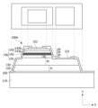
도 1은 제1 실시예에 따른 반도체 소자의 평면도와 단면도를 도시한 도면이다.1 is a diagram illustrating a plan view and a cross-sectional view of a semiconductor device according to a first embodiment.
도 1을 참조하면, 제1 실시예에 따른 반도체 소자(100A)는 기판(110), 기판(110) 상에 배치되는 희생층(120), 희생층(120) 상에 배치되는 결합층(130), 제1 도전형 반도체층(141), 제2-2 도전형 반도체층(143b) 및 제1 도전형 반도체층(141)과 제2-2 도전형 반도체층(143b) 사이에 배치되는 활성층(142)을 포함하고 결합층(130) 상에 배치되는 발광구조물(140), 제1 도전형 반도체층(141)과 연결되는 제1 전극(151), 제2-2 도전형 반도체층(143b)과 연결되는 제2 전극(152) 및 결합층(130)과 발광구조물(140)을 덮는 보호층(160)을 포함할 수 있다.Referring to FIG. 1, the
기판(110)은 도전성 물질로 이루어질 수 있다. 예시적으로 기판(110)은 금속 또는 반도체 물질을 포함할 수 있다. 기판(110)은 전기 전도도 및/또는 열 전도도가 우수한 금속일 수 있다. 이 경우 반도체 소자(100A) 동작시 발생하는 열을 신속이 외부로 방출할 수 있다.The
기판(110)은 아래 도 2a 내지 도 2i에서 설명하는 제3 기판과 동일하다. 기판(110)은 GaAs, 사파이어(Al2O3), SiC, Si, GaN, ZnO, GaP, InP, Ge, 및 Ga203 중 어느 하나를 포함할 수 있다. The
희생층(120)은 기판(110) 상에 배치될 수 있다. 희생층(120)은 반도체 장치를 디스플레이 장치로 전사하면서 제거될 수 있다. 예컨대, 반도체 장치가 디스플레이 장치로 전사되는 경우 희생층(120)은 전사 시 조사되는 레이저에 의해 분리될 수 있다. 이 때, 희생층(120)은 조사된 레이저의 파장에서 분리되도록 형성될 수 있다. 또한, 레이저의 파장은 532㎚ 또는 1064㎚일 수 있다.The
희생층(120)은 산화물(oxide) 또는 질화물(nitride)을 포함할 수 있다. 다만, 이에 한정되는 것은 아니다.희생층(120)은 SOG 박막(Spin on Glass)인 경우, 실리케이트 또는 실릭산 타입일 수 있다. 희생층(120)은 SOD(Spin On Dielectrics) 박막인 경우, silicate, siloxane, methyl silsequioxane(MSQ), hydrogen silsequioxane(HSQ), MQS + HSQ, perhydrosilazane(TCPS) 또는 polysilazane을 포함할 수 있다. 다만, 이에 한정되는 것은 아니다.The
희생층(120)은 E-빔 증착법(E-beam evaporator), 열 증착법(thermal evaporator), MOCVD(Metal Organic Chemical Vapor Deposition), 스퍼터링(Sputtering) 및 PLD(Pulsed Laser Deposition)법으로 형성될 수 있으나, 이에 한정되지 않는다.The
결합층(130)은 희생층(120) 상에 배치될 수 있다. 다만, 이에 한정되는 것은 아니며, 희생층(120) 하부에 배치될 수도 있다. 결합층(130)은 C, O, N 및 H 중 어느 하나를 포함할 수 있으며, 결합층(130)은 레진을 포함할 수 있으나, 이에 한정되는 것은 아니다.The
결합층(130)의 두께(d1)는 1.8㎛ 내지 2.2㎛일 수 있다. 다만, 이에 한정되는 것은 아니다. 여기서, 두께는 Y축 방향의 길이일 수 있다.The thickness d1 of the
발광구조물(140)은 결합층(130) 상에 배치될 수 있다.The
발광구조물(140)은 제1 도전형 반도체층(141), 제2-2 도전형 반도체층(143b) 및 제1 도전형 반도체층(141)과 제2-2 도전형 반도체층(143b) 사이에 배치되는 활성층(142)을 포함할 수 있다.The
제1 도전형 반도체층(141)은 결합층(130) 상에 배치될 수 있다. 제1 도전형 반도체층(141)의 두께(d2)는 1.8㎛ 내지 2.2㎛일 수 있다. 다만, 이에 한정되는 것은 아니다.The first
제1 도전형 반도체층(141)은 Ⅲ-Ⅴ족, Ⅱ-Ⅵ족 등의 화합물 반도체로 구현될 수 있으며, 제1도펀트가 도핑될 수 있다. 제1 도전형 제1 반도체층(112)은 InxAlyGa1-x-yP (0≤x≤1, 0≤y≤1, 0≤x+y≤1) 또는 InxAlyGa1-x-yN (0≤x≤1, 0≤y≤1, 0≤x+y≤1)의 조성식을 갖는 반도체 물질을 포함할 수 있다.The first
그리고, 제1 도펀트는 Si, Ge, Sn, Se, Te와 같은 n형 도펀트일 수 있다. 제1 도펀트가 n형 도펀트인 경우, 제1 도펀트가 도핑된 제1 도전형 반도체층(141)은 n형 반도체층일 수 있다.And, the first dopant may be an n-type dopant such as Si, Ge, Sn, Se, or Te. When the first dopant is an n-type dopant, the first
제1 도전형 반도체층(141)은 AlGaP, InGaP, AlInGaP, InP, GaN, InN, AlN, InGaN, AlGaN, InAlGaN, AlInN, AlGaAs, InGaAs, AlInGaAs, GaP 중 어느 하나 이상을 포함할 수 있다. The first
제1 도전형 반도체층(141)은 화학증착방법(CVD) 혹은 분자선 에피택시 (MBE) 혹은 스퍼터링 혹은 수산화물 증기상 에피택시(HVPE) 등의 방법을 사용하여 형성될 수 있으나, 이에 한정되는 것은 아니다.The first
제1 도전형 반도체층(141) 상에 제1 전극(151)이 배치될 수 있다. 제1 도전형 반도체층(141)은 제1 전극(151)과 전기적으로 연결될 수 있다.A
제1 전극(151)은 제1 도전형 반도체층(141) 상면의 일부분에 배치될 수 있다. 제1 전극(151)은 제2 전극(152)보다 하부에 배치될 수 있다.The
제1 전극(151)은 ITO(indium tin oxide), IZO(indium zinc oxide), IZTO(indium zinc tin oxide), IAZO(indium aluminum zinc oxide), IGZO(indium gallium zinc oxide), IGTO(indium gallium tin oxide), AZO(aluminum zinc oxide), ATO(antimony tin oxide), GZO(gallium zinc oxide), IZON(IZO Nitride), AGZO(Al-Ga ZnO), IGZO(In-Ga ZnO), ZnO, IrOx, RuOx, NiO, RuOx/ITO, Ni/IrOx/Au, 또는 Ni/IrOx/Au/ITO, Ag, Ni, Cr, Ti, Al, Rh, Pd, Ir, Sn, In, Ru, Mg, Zn, Pt, Au, Hf 중 적어도 하나를 포함하여 형성될 수 있으나, 이러한 재료에 한정되는 않는다. The
제1 전극(151)은 스터퍼링, 코팅, 증착 등과 같이 통상적으로 사용되는 전극 형성 방법이 모두 적용될 수 있다. The
제1 클래드층(144)은 제1 도전형 반도체층(141) 상에 배치될 수 있다. 제1 클래드층(144)은 제1 도전형 반도체층(141)과 활성층(142) 사이에 배치될 수 있다. 제1 클래드층(144)은 복수 개의 층을 포함할 수 있다. 제1 클래드층(144)은 AlInP 계열층/AlInGaP 계열층을 포함할 수 있다. The first
제1 클래드층(144)의 두께(d3)는 0.45㎛ 내지 0.55㎛일 수 있다. 다만, 이에 한정되는 것은 아니다.The thickness d3 of the first
활성층(142)은 제1 클래드층(144) 상에 배치될 수 있다. 활성층(142)은 제1 도전형 반도체층(141)과 제2-2 도전형 반도체층(143b) 사이에 배치될 수 있다. 활성층(142)은 제1 도전형 반도체층(141)을 통해서 주입되는 전자(또는 정공)와 제2-1 도전형 반도체층(143a)을 통해서 주입되는 정공(또는 전자)이 만나는 층이다. 활성층(142)은 전자와 정공이 재결합함에 따라 낮은 에너지 준위로 천이하며, 자외선 파장을 가지는 빛을 생성할 수 있다.The
활성층(142)은 단일 우물 구조, 다중 우물 구조, 단일 양자 우물 구조, 다중 양자 우물(Multi Quant㎛ Well; MQW) 구조, 양자점 구조 또는 양자선 구조 중 어느 하나의 구조를 가질 수 있으며, 활성층(142)의 구조는 이에 한정하지 않는다.The
활성층(142)은 GaInP/AlGaInP, GaP/AlGaP, InGaP/AlGaP, InGaN/GaN, InGaN/InGaN, GaN/AlGaN, InAlGaN/GaN, GaAs/AlGaAs,InGaAs/AlGaAs 중 어느 하나 이상의 페어 구조로 형성될 수 있으나 이에 한정되지 않는다. The
활성층(142)의 두께(d4)는 0.54㎛ 내지 0.66일 수 있다. 다만, 이에 한정되는 것은 아니다.The thickness d4 of the
제1 클래드층(144)에서 전자가 냉각되어 활성층(142)은 더 많은 발광재결합(Radiation Recombination)을 발생시킬 수 있다.As electrons are cooled in the first
제2 도전형 반도체층(143)은 활성층(142) 상에 배치될 수 있다. 제2 도전형 반도체층(143)은 제2-1 도전형 반도체층(143a)과 제2-2 도전형 반도체층(143b)을 포함할 수 있다.The second
제2-1 도전형 반도체층(143a)은 활성층(142) 상에 배치될 수 있다. 제2-2 도전형 반도체층(143b)은 제2-1 도전형 반도체층(143a) 상에 배치될 수 있다.The 2-1 conductivity
제2-1 도전형 반도체층(143a)은 TSBR, P-AllnP를 포함할 수 있다. 제2-1 도전형 반도체층(143a)의 두께(d5)는 0.57㎛ 내지 0.70㎛일 수 있다. 다만, 이에 한정되는 것은 아니다.The 2-1st conductivity
제2-1 도전형 반도체층(143a)은 Ⅲ-Ⅴ족, Ⅱ-Ⅵ족 등의 화합물 반도체로 구현될 수 있다. 제2-1 도전형 반도체층(143a)에 제2 도펀트가 도핑될 수 있다. The 2-1 conductivity
제2-1 도전형 반도체층(143a)은 InxAlyGa1-x-yP (0≤x≤1, 0≤y≤1, 0≤x+y≤1) 또는 InxAlyGa1-x-yN (0≤x≤1, 0≤y≤1, 0≤x+y≤1)의 조성식을 갖는 반도체 물질을 포함할 수 있다. 제2 도전형 반도체층(143)이 p형 반도체층인 경우, p형 도펀트로서, Mg, Zn, Ca, Sr, Ba 등을 포함할 수 있다.The 2-1 conductivity
제2-1 도전형 반도체층(143a)은 제2 도펀트가 도핑된 제2-1 도전형 반도체층(143a)은 p형 반도체층일 수 있다.The 2-1st conductivity
제2-2 도전형 반도체층(143b)은 제2-1 도전형 반도체층(143a) 상에 배치될 수 있다. 제2-2 도전형 반도체층(143b)은 p형 GaP 계열층을 포함할 수 있다.The 2-2nd conductivity
제2-2 도전형 반도체층(143b)은 GaP층/InxGa1-xP층(단, 0≤x≤1)의 초격자구조를 포함할 수 있다.The 2-2nd conductivity
예를 들어, 제2-2 도전형 반도체층(143b)에는 약 10X10-18 농도의 Mg이 도핑될 수 있으나, 이에 한정되지 않는다.For example, the 2-2 conductivity
또한, 제2-2 도전형 반도체층(143b)은 복수의 층으로 이루어져 일부 층에만 Mg이 도핑될 수도 있다.Additionally, the 2-2nd conductivity
제2-2 도전형 반도체층(143b)의 두께(d6)는 0.9㎛ 내지 1.1㎛일 수 있다. 다만, 이에 한정되는 것은 아니다.The thickness d6 of the 2-2 conductive
제2 전극(152)은 제2-2 도전형 반도체층(143b) 상에 배치될 수 있다. 제2 전극(152)은 제2-2 도전형 반도체층(143b)과 전기적으로 연결될 수 있다.The
제2 전극(152)은 ITO(indium tin oxide), IZO(indium zinc oxide), IZTO(indium zinc tin oxide), IAZO(indium aluminum zinc oxide), IGZO(indium gallium zinc oxide), IGTO(indium gallium tin oxide), AZO(aluminum zinc oxide), ATO(antimony tin oxide), GZO(gallium zinc oxide), IZON(IZO Nitride), AGZO(Al-Ga ZnO), IGZO(In-Ga ZnO), ZnO, IrOx, RuOx, NiO, RuOx/ITO, Ni/IrOx/Au, 또는 Ni/IrOx/Au/ITO, Ag, Ni, Cr, Ti, Al, Rh, Pd, Ir, Sn, In, Ru, Mg, Zn, Pt, Au, Hf 중 적어도 하나를 포함하여 형성될 수 있으나, 이러한 재료에 한정되는 않는다. The
제2 전극(152)은 스터퍼링, 코팅, 증착 등과 같이 통상적으로 사용되는 전극 형성 방법이 모두 적용될 수 있다. The
보호층(160)은 결합층(130), 희생층(120) 및 발광구조물(140) 덮을 수 있다. 보호층(160)은 희생층(120)의 측면, 결합층(130)의 측면 및 발광구조물(140)의 측면을 덮을 수 있다. 결합층(130), 희생층(120) 및 발광구조물(140)은 노출되지 않을 수 있다.The
보호층(160)은 제1 전극(151)의 상면의 일부를 덮을 수 있다. 또한, 보호층(160)은 제2 전극(152)의 상면의 일부를 덮을 수 있다. 제1 전극(151)의 상면 일부는 노출될 수 있다. 제2 전극(152)의 상면 일부는 노출될 수 있다.The
보호층(160)은 절연층일 수 있다. 보호층(160)은 SiO2, SixOy, Si3N4, SixNy, SiOxNy, Al2O3, TiO2, AlN 등으로 이루어진 군에서 적어도 하나가 선택되어 형성될 수 있으나, 이에 한정하지 않는다. The
도 2a 내지 2i는 제1 실시예에 따른 반도체 소자의 제조 방법을 도시한 도면이다. 2A to 2I are diagrams showing a method of manufacturing a semiconductor device according to the first embodiment.
제1 실시예에 따른 반도체 소자의 제조 방법은 기판 상부에 결합층(130)을 배치하고, 제1 도전형 반도체층(141), 제2 도전형 반도체층(143) 및 제1 도전형 반도체층(141)과 제2 도전형 반도체층(143) 사이에 배치되는 활성층(142)을 포함하고 결합층(130) 상에 배치되는 발광구조물(140)을 배치하는 단계; 발광구조물(140) 상에 제2 기판(2)을 배치하는 단계; 제1 기판(1)을 분리하는 단계; 발광구조물(140) 상에 결합층(130)을 배치하고, 결합층(130) 상에 제3 기판(110)을 배치하는 단계; 제2 기판(2)을 분리하는 단계; 발광구조물(140)의 제1 도전형 반도체층(141)의 일부 영역까지 1차 식각하는 단계; 제1 도전형 반도체층(141) 상에 제1 전극(151)을 배치하고, 제2 도전형 반도체층(143) 상에 제2 전극(152)을 배치하는 단계; 제3 기판(110) 상부까지 2차 식각하는 단계; 및 결합층(130) 및 발광구조물(140)을 덮는 보호층(160)을 배치하는 단계;를 포함할 수 있다.The method of manufacturing a semiconductor device according to the first embodiment includes disposing the
먼저, 도 2a를 참조하면, 반도체 소자는 제1 기판(1)과 발광구조물(140)을 포함할 수 있다. 제1 기판(1) 및 제1 기판(1) 상에 발광구조물(140)을 배치할 수 있다. First, referring to FIG. 2A, the semiconductor device may include a
발광구조물(140)은 제1 도전형 반도체층(141), 제1 도전형 반도체층(141) 상에 배치되는 제1 클래드층(144), 제1 클래드층(144) 상에 배치되는 활성층(142), 활성층(142) 상에 배치되는 제2-1 도전형 반도체층(143a), 제2-1 도전형 반도체층(143a) 상에 배치되는 제2-2 도전형 반도체층(143b)을 포함할 수 있다.The
제1 기판(1)은 열전도성이 뛰어난 물질을 포함할 수 있다. 제1 기판(1)은 전도성 기판 또는 절연성 기판일수 있다. 예를 들어, 제1 기판(1)은 GaAs, 사파이어(Al2O3), SiC, Si, GaN, ZnO, GaP, InP, Ge, 및 Ga203 중 적어도 하나를 사용할 수 있다.The
제1 기판(1) 상에 요철 구조가 형성될 수 있으나, 이에 대해 한정하지는 않는다. 제1 기판(1)에 대해 습식세척을 하여 표면의 불순물을 제거할 수 있다.A concavo-convex structure may be formed on the
제1 기판(1) 상에 제1 도전형 반도체층(141)이 배치될 수 있다. 그리고 제1 도전형 반도체층(141) 상에 제1 클래드층(144)이 배치될 수 있다. 제1 도전형 제1 반도체층은 화학증착방법(CVD) 혹은 분자선 에피택시 (MBE) 혹은 스퍼터링 혹은 수산화물 증기상 에피택시(HVPE) 등의 방법에 의해 형성될 수 있으나, 이에 한정되는 것은 아니다.A first
그리고 활성층(142)은 제1 클래드층(144) 상에 배치될 수 있다. 또한, 제2 도전형 반도체층(143)은 활성층(142) 상에 배치될 수 있다. 제2-1 도전형 반도체층(143a)이 활성층(142) 상에 배치될 수 있다. 그리고 제2-2 도전형 반도체층(143b)은 제2-1 도전형 반도체층(143a) 상에 배치될 수 있다.And the
그 다음 도 2b를 참조하면, 제2 기판(2)은 반도체 소자(100A) 상부에 배치될 수 있다. 제2 기판(2)은 제2-2 도전형 반도체층(143b) 상에 배치될 수 있다. 제2 기판(2)은 도전성 기판 및/또는 절연성 기판일 수 있다. 제2 기판(2)은 사파이어 기판을 포함할 수 있으나, 이에 한정되는 것은 아니다.Next, referring to FIG. 2B, the
도 2c 및 도 2d를 참조하면, 제1 기판(1)은 반도체 소자(100A)로부터 분리될 수 있다. 예시적으로, 제1 기판(1)은 레이저 리프트 오프 등의 공정에 의해 제거될 수 있다. Referring to FIGS. 2C and 2D , the
그리고 제1 도전형 반도체층(141) 상에 결합층(130)이 배치될 수 있다. 그리고 결합층(130) 상에 희생층(120)이 배치될 수 있다. 또한, 희생층(120) 상에 제3 기판(110)이 배치될 수 있다. And the
희생층(120)은 SiO2, SiNx, TiO2, 폴리이미드 등을 물질을 포함할 수 있다. 희생층(120)은 PECVD, MOCVD 등과 같은 통상의 에피텍셜 박막 형성법이나 스핀 코팅법(폴리이미드의 경우)에 의해 형성될 수 있다. 다만, 이에 한정되는 것은 아니다.The
결합층(130)은 레진을 포함할 수 있으나, 이에 한정되는 것은 아니다.The
제3 기판(110)은 희생층(120) 상에 배치될 수 있다. 제3 기판(110)은 발광구조물(140), 결합층(130) 및 희생층(120)을 지지하는 지지체의 역할을 수행할 수 있다. Au, Ni, Al, Cu, W, Si, Se, O, GaAs 중 어느 하나를 포함하는 물질, 예컨대, 제3 기판(110)은 사파이어 기판일 수 있으나, 이에 한정되는 것은 아니다. 또한, 제3 기판(110)은 디스플레이 장치로 전사되는 경우에 조사되는 레이저가 투과되도록 형성될 수 있다. 예컨대, 조사되는 레이저 파장이 532㎚ 또는 1064㎚인 경우, 제 532㎚ 또는 1064㎚ 파장의 레이저는 제3 기판(110)를 투과하여 희생층(120)에서 흡수되고, 희생층(120)은 조사된 레이저에 의해 분리될 수 있다.The
도 2e를 참조하면, 제2 기판(2)은 레이저 리프트 오프(Laser Lift Off, LLO)에 의해 제거될 수 있다. Referring to FIG. 2E, the
도 2f를 참조하면, 발광구조물(140)의 상부에서 제1 도전형 반도체층(141)의 일부까지 1차 식각이 수행될 수 있다. Referring to FIG. 2F, a primary etch may be performed from the top of the
1차 식각은 습식식각 또는 건식식각에 의할 수 있으나 이에 한정되는 것은 아니다. The first etching may be wet etching or dry etching, but is not limited thereto.
도 2g를 참조하면, 발광구조물(140) 상부에 제2 전극(152)이 배치될 수 있다. 제2 전극(152)은 제2-2 도전형 반도체층(143b)과 전기적으로 연결될 수 있다. Referring to FIG. 2G, the
제1 전극(151) 및 제2 전극(152)은 스터퍼링, 코팅, 증착 등과 같이 통상적으로 사용되는 전극 형성 방법이 모두 적용될 수 있다. 다만, 이에 한정되지 않는다.The
제1 전극(151)과 제2 전극(152)은 제3 기판(110)으로부터 서로 상이한 위치에 배치될 수 있다. 제1 전극(151)은 제1 도전형 반도체층(141) 상에 배치될 수 있다. 제2 전극(152)은 제2-2 도전형 반도체층(143b) 상에 배치될 수 있다. 이에, 제1 전극(151)보다 상부에 제2 전극(152)이 배치될 수 있다. 다만, 이에 한정되지 않는다.The
예를 들어, 제2 도전형 반도체층(143) 상에 제1 도전형 반도체층(141)이 배치되는 경우, 제1 전극(151)이 제2 전극(152)보다 상부에 배치될 수 있다.For example, when the first conductivity
제1 도전형 반도체층(141) 상에 이 배치될 수 있다. 제1 전극(151)은 제1 도전형 반도체층(141)과 전기적으로 연결될 수 있다.It may be disposed on the first
도 2h를 참조하면, 제3 기판(110)의 상면까지 2차 식각이 수행될 수 있다. 2차 식각은 습식식각 또는 건식식각에 의할 수 있으나 이에 한정되는 것은 아니다. Referring to FIG. 2H, secondary etching may be performed up to the top surface of the
2차 식각은 1차 식각보다 큰 두께를 식각할 수 있으나, 이에 한정되지 않는다. 예컨대, 2차 식각은 희생층(120) 또는 결합층(130)까지 수행될 수 있다.The secondary etching may etch a greater thickness than the primary etching, but is not limited to this. For example, secondary etching may be performed up to the
2차 식각을 통해 제3 기판(110) 상에 배치된 반도체 소자는 복수 개의 칩(chip) 형태로 아이솔레이션(Isolation)될 수 있다. Semiconductor devices disposed on the
도 2i를 참조하면, 희생층(120), 결합층(130) 및 발광구조물(140)을 덮도록 보호층(160)을 덮을 수 있다. Referring to FIG. 2I, the
보호층(160)은 희생층(120), 결합층(130) 및 발광구조물(140)의 측면을 덮을 수 있다. 보호층(160)은 제1 전극(151)의 상면 일부까지 덮을 수 있다. 제1 전극(151)의 상면 일부는 노출될 수 있다.The
보호층(160)은 제2 전극(152)의 상면 일부까지 덮을 수 있다. 제2 전극(152)의 상면 일부는 노출될 수 있다.The
보호층(160)의 일부는 제3 기판(110)의 상면에 배치될 수 있다. 인접한 반도체 칩 사이에 보호층(160)의 일부가 배치될 수 있다.A portion of the
도 3는 본 발명의 제2 실시예에 따른 반도체 소자(100B)의 평면도와 단면도를 도시한 도면이다.FIG. 3 is a plan view and cross-sectional view of a
도 3을 참조하면, 본 발명의 제2 실시예에 반도체 소자(100B)는 기판, 기판 상에 배치되는 희생층(120), 희생층(120) 상에 배치되는 결합층(130), 제1 도전형 반도체층(141), 제2-2 도전형 반도체층(143b) 및 제1 도전형 반도체층(141)과 제2-2 도전형 반도체층(143b) 사이에 배치되는 활성층(142)을 포함하고 결합층(130) 상에 배치되는 발광구조물(140), 제1 도전형 반도체층(141)과 연결되는 제1 전극(151), 제2-2 도전형 반도체층(143b)과 연결되는 제2 전극(152) 및 결합층(130)과 발광구조물(140)을 덮는 보호층(160)을 포함할 수 있다.Referring to FIG. 3, in the second embodiment of the present invention, the
기판, 희생층(120) 및 결합층(130)은 도 1에서 설명한 바와 동일하게 적용될 수 있다.The substrate,
발광구조물(140)은 결합층(130) 상에 배치될 수 있다.The
발광구조물(140)은 제1 도전형 반도체층(141), 제2-2 도전형 반도체층(143b) 및 제1 도전형 반도체층(141)과 제2-2 도전형 반도체층(143b) 사이에 배치되는 활성층(142)을 포함할 수 있다.The
제2-2 도전형 반도체층(143b)은 결합층(130) 상에 배치될 수 있다. 제2-2 도전형 반도체층(143b)의 두께(d7)는 3.15㎛ 내지 3.85㎛일 수 있다. 다만, 이에 한정되는 것은 아니다.The 2-2nd conductivity
제2-2 도전형 반도체층(143b)은 제2-1 도전형 반도체층(143a) 상에 배치될 수 있다. 제2-2 도전형 반도체층(143b)은 p형 GaP 계열층을 포함할 수 있다.The 2-2nd conductivity
제2-2 도전형 반도체층(143b)은 GaP층/InxGa1-xP층(단, 0≤x≤1)의 초격자구조를 포함할 수 있다.The 2-2nd conductivity
제2-2 도전형 반도체층(143b) 상에 제2 전극(152)이 배치될 수 있다. 제2-2 도전형 반도체층(143b)은 제2 전극(152)과 전기적으로 연결될 수 있다.The
제2 전극(152)은 제2-2 도전형 반도체층(143b) 상면의 일측에 배치될 수 있다. 제2 전극(152)은 제1 전극(151)보다 하부에 위치할 수 있다.The
제2-1 도전형 반도체층(143a)은 제2-2 도전형 반도체층(143b) 상에 배치될 수 있다. 제2-1 도전형 반도체층(143a)은 제2-2 도전형 반도체층(143b)과 활성층(142) 사이에 배치될 수 있다.The 2-1st conductivity
제2-1 도전형 반도체층(143a)의 두께(d8)는 0.57㎛ 내지 0.69㎛일 수 있다. 다만, 이에 한정되는 것은 아니다. 제2-1 도전형 반도체층(143a)은 InxAlyGa1-x-yP (0≤x≤1, 0≤y≤1, 0≤x+y≤1) 또는 InxAlyGa1-x-yN (0≤x≤1, 0≤y≤1, 0≤x+y≤1)의 조성식을 갖는 반도체 물질을 포함할 수 있다. 상기 제2 도전형 반도체층(143)이 p형 반도체층인 경우, p형 도펀트로서, Mg, Zn, Ca, Sr, Ba 등을 포함할 수 있다.The thickness d8 of the 2-1 conductivity
제2-1 도전형 반도체층(143a)은 제2 도펀트가 도핑된 제2-1 도전형 반도체층(143a)은 p형 반도체층일 수 있다. 제2-1 도전형 반도체층(143a)은 TSBR, AlInP를 포함할 수 있다.The 2-1st conductivity
활성층(142)은 제2-1 도전형 반도체층(143a) 상에 배치될 수 있다. 활성층(142)은 제1 도전형 반도체층(141)을 통해서 주입되는 전자(또는 정공)와 제2-1 도전형 반도체층(143a)을 통해서 주입되는 정공(또는 전자)이 만나는 층이다. 활성층(142)은 전자와 정공이 재결합함에 따라 낮은 에너지 준위로 천이하며, 자외선 파장을 가지는 빛을 생성할 수 있다.The
활성층(142)은 단일 우물 구조, 다중 우물 구조, 단일 양자 우물 구조, 다중 양자 우물(Multi Quant㎛ Well; MQW) 구조, 양자점 구조 또는 양자선 구조 중 어느 하나의 구조를 가질 수 있으며, 활성층(142)의 구조는 이에 한정하지 않는다.The
활성층(142)은 GaInP/AlGaInP, GaP/AlGaP, InGaP/AlGaP, InGaN/GaN, InGaN/InGaN, GaN/AlGaN, InAlGaN/GaN, GaAs/AlGaAs,InGaAs/AlGaAs 중 어느 하나 이상의 페어 구조로 형성될 수 있으나 이에 한정되지 않는다. The
활성층(142)의 두께(d9)는 0.54㎛ 내지 0.66일 수 있다. 다만, 이에 한정되는 것은 아니다.The thickness d9 of the
제1 클래드층(144)은 활성층(142) 상에 배치될 수 있다. 제1 클래드는 활성층(142)과 제1 도전형 반도체층(141) 사이에 배치될 수 있다.The first
제1 클래드층(144)은 AlInP를 포함할 수 있다. 제1 클래드층(144)의 두께(d10)는 0.45㎛ 내지 0.55㎛일 수 있다. 다만, 이에 한정되는 것은 아니다.The first
제1 도전형 반도체층(141)은 제1 클래드층(144) 상에 배치될 수 있다. 제1 도전형 반도체층(141)은 Ⅲ-Ⅴ족, Ⅱ-Ⅵ족 등의 화합물 반도체로 구현될 수 있으며, 제1도펀트가 도핑될 수 있다. 제1 도전형 제1 반도체층(112)은 InxAlyGa1-x-yP (0≤x≤1, 0≤y≤1, 0≤x+y≤1) 또는 InxAlyGa1-x-yN (0≤x≤1, 0≤y≤1, 0≤x+y≤1)의 조성식을 갖는 반도체 물질을 포함할 수 있다.The first
그리고, 제1도펀트는 Si, Ge, Sn, Se, Te와 같은 n형 도펀트일 수 있다. 제1 도펀트가 n형 도펀트인 경우, 제1 도펀트가 도핑된 제1 도전형 반도체층(141)은 n형 반도체층일 수 있다.And, the first dopant may be an n-type dopant such as Si, Ge, Sn, Se, or Te. When the first dopant is an n-type dopant, the first
제1 도전형 반도체층(141)은 AlGaP, InGaP, AlInGaP, InP, GaN, InN, AlN, InGaN, AlGaN, InAlGaN, AlInN, AlGaAs, InGaAs, AlInGaAs, GaP 중 어느 하나 이상을 포함할 수 있다. The first
제1 도전형 반도체층(141)은 화학증착방법(CVD) 혹은 분자선 에피택시 (MBE) 혹은 스퍼터링 혹은 수산화물 증기상 에피택시(HVPE) 등의 방법을 사용하여 형성될 수 있으나 이에 한정되는 것은 아니다.The first
제1 도전형 반도체층(141)의 두께(d11)는 0.45㎛ 내지5.5㎛일 수 있다. 다만, 이에 한정되는 것은 아니다.The thickness d11 of the first
제1 전극(151)은 제1 도전형 반도체층(141) 상에 배치될 수 있다. 제1 전극(151)은 제1 도전형 반도체층(141)과 전기적으로 연결될 수 있다. 제1 전극(151)은 제2 전극(152) 상부에 위치할 수 있다.The
보호층(160)은 희생층(120), 결합층(130) 및 발광구조물(140)을 덮을 수 있다. 보호층(160)은 희생층(120), 결합층(130) 및 발광구조물(140)의 측면을 덮을 수 있다.The
보호층(160)은 제1 전극(151)의 상면의 일부를 덮을 수 있다. 제1 전극(151)의 상면 일부는 노출될 수 있다.The
보호층(160)은 제2 전극(152)의 상면의 일부를 덮을 수 있다. 제2 전극(152)의 상면 일부는 노출될 수 있다.The
도 4는 제1 실시예에 따른 반도체 소자의 변형예의 단면도를 도시한 도면이다.FIG. 4 is a cross-sectional view of a modified example of the semiconductor device according to the first embodiment.
도 4를 참조하면, 제1 실시예에 따른 반도체 소자의 변형예(100A')에서 결합층(130)과 희생층(120)은 위치가 서로 바뀔 수 있다. 그리고 결합층(130)과 희생층(120)은 반도체 소자로부터 분리될 수 있다. 이러한 구성에 의해, 디스플레이 장치의 패널로 배치되는 반도체 칩은 발광구조물(140)만을 포함하거나, 발광구조물(140)과 결합층 및 희생층 중 중 어느 하나를 포함한 형태일 수 있다.Referring to FIG. 4, in the modified example 100A' of the semiconductor device according to the first embodiment, the positions of the
도 5는 제3 실시예에 따른 반도체 소자의 단면도이고, 도 6a 내지 도 6f는 제3 실시예에 따른 반도체 소자의 제조 방법을 도시한 도면이다.FIG. 5 is a cross-sectional view of a semiconductor device according to a third embodiment, and FIGS. 6A to 6F are diagrams showing a method of manufacturing a semiconductor device according to a third embodiment.
도 5를 참조하면, 제3 실시예에 따른 반도체 소자(100C)는 기판(110), 기판(110) 상에 배치되는 희생층(120), 희생층(120) 상에 배치되는 결합층(130), 결합층(130) 상에 배치되는 제4 기판(170), 제1 도전형 반도체층(141), 제2-2 도전형 반도체층(143b) 및 제1 도전형 반도체층(141)과 제2-2 도전형 반도체층(143b) 사이에 배치되는 활성층(142)을 포함하고 제4 기판(170) 상에 배치되는 발광구조물(140), 제1 도전형 반도체층(141)과 연결되는 제1 전극(151), 제2-2 도전형 반도체층(143b)과 연결되는 제2 전극(152) 및 결합층(130)과 발광구조물(140)을 덮는 보호층(160)을 포함할 수 있다.Referring to FIG. 5, the
기판(110), 희생층(120), 결합층(130) 및 발광구조물(140), 제1 전극(151) 및 제2 전극은 도 1에서 설명한 바와 동일하게 적용될 수 있다. 여기서, 제4 기판은 GaAs 기판일 수 있다.The
도 6a를 참조하면, 제4 기판(170)에 이온을 주입하여 제4 기판(170)은 이온층(I)을 포함할 수 있다. 이온은 수소(H)이온을 포함할 수 있으나, 이에 한정되는 것은 아니다.Referring to FIG. 6A , ions are implanted into the
이온층(I)은 제4 기판(170)의 일면으로부터 소정의 거리 이격 배치될 수 있다. 이에, 제4 기판(170)은 제4-1 기판(170a)와 제4-2 기판(170b)를 포함할 수 있다. 이온층(I)은 제4 기판(170)의 일면으로부터 0.4㎛ 내지 0.6㎛ 이격되어 형성될 수 있다. 즉, 제4-1 기판(170a)의 두께는 0.4㎛ 내지 0.6㎛일 수 있다.The ion layer (I) may be disposed at a predetermined distance from one surface of the
도 6b를 참조하면, 앞서 도2d에서 설명한 바와 같이 기판(110)과 결합층(130) 사이에 희생층(120)이 배치될 수 있다. 그리고 결합층(130) 상에 제4-1 기판(170a)이 배치되고, 결합층(130)과 제4-1 기판(170a)가 결합할 수 있다.Referring to FIG. 6B, the
결합층(130)은 SiO2를 포함할 수 있으며, 결합층(130)은 제4-1 기판(170a)와 O2 플라즈마 처리를 통해 결합될 수 있다.The
이로써, 기판(110) 상에 희생층(120)이 배치되고, 희생층(120) 상에 결합층(130)이 배치되고, 결합층(130) 상에 제4-1 기판(170a)이 배치되고, 제4-1 기판(170a) 상에 이온층(I) 및 제4-2 기판(170b)이 배치될 수 있다.Accordingly, the
도 6c를 참조하면, 결합층(130) 상에 제4 기판(170)이 배치될 수 있다. 도 6b의 이온층(I)은 유체 분사 절삭(Fluid jet cleaving)에 의해 제거되어, 제4-2 기판(170b)은 제4-1 기판(170a)과 분리될 수 있다.Referring to FIG. 6C, the
분리된 제4-2 기판(170b)은 기판으로 재사용될 수 있다. 이로써, 제조 비용 및 원가 절감의 효과를 제공할 수 있다.The separated 4-2
이에 따라, 결합층(130) 상에 배치된 제4 기판(170)은 도 6b의 제4-1 기판(170a)을 의미하나, 이하에서 제4 기판(170)으로 설명하겠다. 그리고 제4 기판(170) 상에 발광구조물(140)이 배치될 수 있다. 제4 기판(170)이 발광구조물(140)과 접촉하는 제4 기판(170)의 상면에 연마가 이루어져 제4 기판(170)의 상면은 평탄할 수 있다. 예컨대, 제4 기판(170)의 상면에 화학적 기계적 평탄화(Chemical Mechanical Planarization)가 수행되고, 평탄화 이후에 제4 기판(170)의 상면에 발광구조물(140)이 배치될 수 있다.Accordingly, the
도 6d를 참조하면, 발광구조물(140)의 상부에서 제1 도전형 반도체층(141)의 일부까지 1차 식각이 수행될 수 있다. 이는 도 2f와 동일하게 적용될 수 있다.Referring to FIG. 6D, a primary etch may be performed from the top of the
1차 식각은 습식식각 또는 건식식각에 의할 수 있으나 이에 한정되는 것은 아니다. The first etching may be wet etching or dry etching, but is not limited thereto.
도 6e를 참조하면, 발광구조물(140) 상부에 제2 전극(152)이 배치될 수 있다. 제2 전극(152)은 제2-2 도전형 반도체층(143b)과 전기적으로 연결될 수 있다. Referring to FIG. 6E, the
제1 전극(151) 및 제2 전극(152)은 스터퍼링, 코팅, 증착 등과 같이 통상적으로 사용되는 전극 형성 방법이 모두 적용될 수 있다. 다만, 이에 한정되지 않는다.The
제1 전극(151)과 제2 전극(152)은 제3 기판(110)으로부터 서로 상이한 위치에 배치될 수 있다. 제1 전극(151)은 제1 도전형 반도체층(141) 상에 배치될 수 있다. 제2 전극(152)은 제2-2 도전형 반도체층(143b) 상에 배치될 수 있다. 이에, 제1 전극(151)보다 상부에 제2 전극(152)이 배치될 수 있다. 다만, 이에 한정되지 않는다.The
예를 들어, 제2 도전형 반도체층(143) 상에 제1 도전형 반도체층(141)이 배치되는 경우, 제1 전극(151)이 제2 전극(152)보다 상부에 배치될 수 있다.For example, when the first conductivity
제1 도전형 반도체층(141) 상에 이 배치될 수 있다. 제1 전극(151)은 제1 도전형 반도체층(141)과 전기적으로 연결될 수 있다. 이는 도 2g에서 설명한 내용이 동일하게 적용될 수 있다.It may be disposed on the first
그리고 제3 기판(110)의 상면까지 2차 식각이 수행될 수 있다. 2차 식각은 습식식각 또는 건식식각에 의할 수 있으나 이에 한정되는 것은 아니다. And secondary etching may be performed up to the top surface of the
2차 식각은 1차 식각보다 큰 두께를 식각할 수 있으나, 이에 한정되지 않는다.The secondary etching may etch a greater thickness than the primary etching, but is not limited to this.
2차 식각을 통해 제3 기판(110) 상에 배치된 반도체 소자는 복수 개의 칩(chip) 형태로 아이솔레이션(Isolation)될 수 있다. 이는 도 2h에서 설명한 내용이 동일하게 적용될 수 있다.Semiconductor devices disposed on the
도 6f를 참조하면, 희생층(120), 결합층(130), 제4 기판(170) 및 발광구조물(140)을 덮도록 보호층(160)을 덮을 수 있다. Referring to FIG. 6F, the
보호층(160)은 희생층(120), 결합층(130), 제4 기판(170) 및 발광구조물(140)의 측면을 덮을 수 있다. 보호층(160)은 제1 전극(151)의 상면 일부까지 덮을 수 있다. 제1 전극(151)의 상면 일부는 노출될 수 있다.The
보호층(160)은 제2 전극(152)의 상면 일부까지 덮을 수 있다. 제2 전극(152)의 상면 일부는 노출될 수 있다. 그리고 보호층(160)의 일부는 제3 기판(110)의 상면에 배치될 수 있다. 인접한 반도체 칩 사이에 보호층(160)의 일부가 배치될 수 있다.도 7a 내지 도 7d는 제1 실시예에 따른 반도체 소자를 이용하여 디스플레이 장치를 제조하는 방법을 도시한 도면이다.The
일실시예에 따른 디스플레이 장치 제조 방법은 기판 상에 배치된 복수 개의 반도체 칩(10)을 포함하는 반도체 소자에 선택적으로 레이저를 조사하여 기판으로부터 반도체 칩(10)을 분리하는 단계, 및 분리된 반도체 칩(10)을 패널 기판에 배치하는 단계를 포함하고, 분리하는 단계에서 발생하는 가스를 배출할 수 있다.A method of manufacturing a display device according to an embodiment includes separating the semiconductor chips 10 from the substrate by selectively irradiating a laser to a semiconductor device including a plurality of
여기서 기판은 상기 제1 실시예에 다른 반도체 소자의 제3 기판(110)일 수 있다. 그리고 분리하는 단계는 복수 개의 반도체 칩(10) 중 적어도 하나를 반송 기구(210)의 하부에 배치된 제1 접합층(211)과 접합하고 기판으로부터 분리할 수 있다.Here, the substrate may be the
또한, 패널 기판에 배치하는 단계는 복수 개의 반도체 칩(10) 중 적어도 하나를 패널 기판 상에 배치하고, 패널 기판 상의 제2 접합층과 접합하는 단계 및 광을 조사하여 제1 접합층(211)과 복수 개의 반도체 칩(10) 중 적어도 하나를 분리하고 제2 접합층과 경화하는 단계를 포함할 수 있다.In addition, the step of placing on the panel substrate includes placing at least one of the plurality of
여기서, 반도체 소자는, 기판; 상기 기판 상에 배치되는 결합층(130); 제1 도전형 반도체층(141), 제2 도전형 반도체층(143) 및 상기 제1 도전형 반도체층(141)과 상기 제2 도전형 반도체층(143) 사이에 배치되는 활성층(142)을 포함하고 상기 결합층(130) 상에 배치되는 발광구조물(140); 상기 제1 도전형 반도체층(141)과 연결되는 제1 전극(151); 상기 제2 도전형 반도체층(143)과 연결되는 제2 전극(152); 및 상기 결합층(130) 및 상기 발광구조물(140)을 덮는 보호층(160);을 포함할 수 있다.Here, the semiconductor device includes: a substrate; A
또한, 기판으로부터 분리하는 단계에서 제1 전극(151)과 제2 전극(152) 및 보호층(160)의 일부는 제1 접합층(211)과 접합할 수 있다.Additionally, in the step of separating from the substrate, the
또한, 제2 접합층(310)과 경화하는 단계에서 반송 기구(210)는 복수 개의 반도체 칩(10) 중 적어도 하나로부터 분리될 수 있다.Additionally, in the step of curing the
상기 디스플레이 장치의 제조 방법과 관련하여 이하 도 7a 내지 도 7d를 바탕으로 설명하겠다.The manufacturing method of the display device will be described below based on FIGS. 7A to 7D.
도 7a를 참조하면, 제1 실시예에 따른 반도체 소자의 제3 기판(110) 상에 레이저광이 조사될 수 있다.Referring to FIG. 7A, laser light may be irradiated onto the
제3 기판(110)을 분리시키기 위하여, 강한 에너지원인 레이저광을 투명한 사파이어 후면(back-side)을 통해서 조사시킬 수 있다. 레이저광은 반도체 소자의 일부 반도체 칩(10)에 조사될 수 있다. 다만, 이에 한정되는 것은 아니며 반도체 소자(100A) 전체 반도체 칩(10)에 조사될 수도 있다.In order to separate the
제3 기판(110)과 결합층(130) 사이에서 레이저 흡수가 일어나고, 이로 인해서 제3 기판(110)과 결합층(130) 사이에 배치된 희생층(120)에서 열화학 분해(thermo-chemical dissolution) 반응이 일어날 수 있다. 이로 인해 일부 반도체 칩(10)은 제3 기판(110)으로부터 분리(lift-off)될 수 있다. 이 때, 희생층(120)의 반응으로 유해 가스가 발생될 수 있다.Laser absorption occurs between the
예시적으로, 유해 가스는 비소(As), 인(P)을 포함할 수 있으며, 이에 한정되지 않는다.By way of example, the harmful gas may include arsenic (As) and phosphorus (P), but is not limited thereto.
실시예에 따른 레이저 리프트 오프 장치를 도시한 도면인 도 9을 참조하면, 실시예에 따른 레이저 리프트 오프 장치(500)는 레이저광을 조사하는 레이저부(510), 레이저광을 조사 위치로 인도하는 광학부(520), 조사 위치에 반도체 소자(100A)가 배치되는 스테이지(530) 및 스테이지(530)를 둘러싸는 수용부(540), 외부를 둘러싸는 하우징(550)을 포함할 수 있다.Referring to FIG. 9 , which is a diagram illustrating a laser lift-off device according to an embodiment, the laser lift-
레이저부(510)는 레이저광을 출사할 수 있다. 예시적으로, 레이저부(510)는 KrF 엑시머 레이저일 수 있으나, 이에 한정되는 것은 아니다.The
레이저원은 펄스 발진일 수 있으나, 이에 한정되는 것은 아니다.The laser source may be pulse oscillating, but is not limited thereto.
광학부(520)는 레이저광을 원하는 패턴으로 조사하기 위한 마스크(522), 마스크(522)에 조사하는 레이저광의 빔을 적당히 확대하거나 정형하는 렌즈군(521)을 포함할 수 있다.The
마스크(522)는 조사 패턴의 형상의 개구를 포함할 수 있다. 예시적으로, 조사 패턴이 방형이면 마스크(522)의 개구도 방형을 가질 수 있다.The
스테이지(530)는 상면에 반도체 소자 위치를 유지하는 부재일 수 있다. 여기서, 반도체 소자(100A)는 상기 언급한 제1 실시예에 따른 반도체 소자일 수 있다. 스테이지(530)는 반도체 소자를 진공 흡착하여 유지하는 기구가 필요에 따라 설치될 수 있으나, 이에 한정되지 않는다.The
또한, 스테이지(530)는 다양한 형상일 수 있다. 예시적으로, 반도체 소자(100A)와 같이 원형일 수 있으나, 이에 한정하지 않는다.Additionally, the
스테이지(530) 상에 배치된 반도체 소자(100A)에 레이저광이 조사될 수 있다. 구체적으로, 제3 기판(110)과 결합층(130) 사이에서 레이저광 흡수가 일어날 수 있다. 제3 기판(110)과 결합층(130) 사이에 배치된 희생층(120)에서 열화학 분해(thermo-chemical dissolution) 반응이 일어날 수 있다. 반도체 소자(100A)에 포함된 복수 개의 반도체 칩(10)은 제3 기판(110)으로부터 분리(lift-off)될 수 있다. 이 때, 희생층(120)의 반응으로 유해 가스가 방출될 수 있다.Laser light may be irradiated to the
도 10은 실시예에 따른 레이저 리프트 오프 장치(500)의 평면도이고, 도 11은 도 10의 레이저 리프트 오프 장치(500)의 평면도의 변형예이다.FIG. 10 is a top view of a laser lift-
도 10및 도 11을 참조하면, 스테이지(530)는 복수 개의 영역으로 구획될 수 있다. 예시적으로 4개의 부분으로 구획될 수 있다.Referring to FIGS. 10 and 11 , the
수용부(540)는 스테이지(530) 외면에 배치되고, 스테이지(530)를 둘러쌀 수 있다. 수용부(540)는 반도체 소자(100A)의 희생층으로부터 배출되는 가스를 방출하는 제1 배기부(541)를 포함할 수 있다.The receiving
제1 배기부(541)는 수용부(540)의 측면에 배치될 수 있다. 또한, 제1 배기부(541)는 복수 개의 배기홀(541a, 541b, 541c, 541d)을 포함할 수 있다.The
복수 개의 배기홀(541a, 541b, 541c, 541d)의 형상은 다양할 수 있다.The shapes of the plurality of
수용부(540)는 스테이지(530)의 복수 개의 영역(S1, S2, S3, S4)과 복수 개의 배기홀(541a, 541b, 541c, 541d) 사이에 형성되는 복수 개의 유로(L1, L2, L3, L4) 를 포함할 수 있다.The receiving
스테이지(530)의 복수 개의 영역(S1, S2, S3, S4)으로부터 배출되는 가스는 복수 개의 유로(L1, L2, L3, L4) 중 어느 하나를 통해 배출될 수 있다.Gas discharged from the plurality of areas (S1, S2, S3, and S4) of the
수용부(540)는 복수 개의 유로(L1, L2, L3, L4) 를 형성하도록 스테이지(530)와 배기홀(541a, 541b, 541c, 541d) 사이에 형성된 복수 개의 격벽(P1, P2, P3, P4)을 포함할 수 있다.The receiving
예시적으로, 제1 영역(S1)으로부터 배출되는 가스는 제1 배기홀(541a)를 통해서만 배출될 수 있다. 다만, 이에 한정되는 것은 아니며 격벽(P1, P2, P3, P4)의 위치 및 수용부의 형상에 따라 다양하게 적용될 수 있다.For example, gas discharged from the first area S1 may be discharged only through the
스테이지(530)에 대해 레이저광의 조사 위치를 이동시키는 이동 기구(미도시됨)를 더 포함할 수 있다.It may further include a moving mechanism (not shown) that moves the irradiation position of the laser light with respect to the
하우징(550)은 레이저부(510), 광학부(520), 스테이지(530) 및 수용부(540)를 둘러쌀 수 있다.The
하우징(550)은 상부에 배치되는 제2 배기부(551)를 포함할 수 있다. 제2 배기부(551)는 제1 배기부(541)를 통해 배출된 가스 중 남아 있는 가스를 배출할 수 있다. 제2 배기부(551)도 복수 개의 배기홀을 포함할 수 있으나, 이에 한정되지 않는다.The
도 12는 실시예에 따른 레이저 리프트 오프 장치(500)의 단면도를 도시한 도면이다.FIG. 12 is a cross-sectional view of a laser lift-
도 12를 참조하면, 반도체 소자(100A)는 스테이지(530) 상에 배치되도록 이동될 수 있다. 이 경우, 반도체 소자(100A)는 이동 장치(미도시됨)에 의해 수용부(540)의 배기홀 상부를 지나 스테이지(530) 상으로 로딩될 수 있다. 그리고 레이저광은 스테이지(530) 상의 반도체 소자(100A)에 조사되고, 희생층(120)은 레이저광의 조사로 제거될 수 있다. 그리고 희생층(120)이 제거되면서, 유해 가스가 방출될 수 있다. 유해 가스는 배기홀로 배출될 수 있다.Referring to FIG. 12, the
도 13은 도 12의 실시예에 다른 레이저 리프트 오프 장치(500)의 단면도의 변형예를 도시한 도면이다.FIG. 13 is a diagram showing a modified example of a cross-sectional view of the laser lift-
도 13을 참조하면, 반도체 소자는 이동 장치(미도시됨)에 의해 배기홀 하부를 지나 스테이지(530) 상으로 로딩될 수 있다. 배기홀 하부에는 이동 슬릿(542)이 배치될 수 있다. Referring to FIG. 13, the semiconductor device may be loaded onto the
이동 슬릿(542)은 반도체 소자(100A)를 스테이지(530) 상으로 로딩하는 경우에 개폐될 수 있다. 레이저광은 스테이지(530) 상의 반도체 소자(100A)에 조사되고, 희생층(120)은 레이저광의 조사로 제거될 수 있다. 그리고 희생층(120)이 희생층(120)이 제거되면서 방출되는 유해 가스는 이동 슬릿(542) 상의 배기부(541)로 배출될 수 있다.The moving
희생층(120)의 제거로 제3 기판(110)으로부터 반도체 칩이 분리될 수 있다. 여기서, 반도체 칩은 상기 도 7a에서 언급한 반도체 칩일 수 있다. 그 다음 반송 기구(210)의 하부에 배치된 제1 접합층(211)은 보호층(160)의 일부, 제1 전극(151) 상면 및 제2 전극(152)의 상면과 접합할 수 있다.The semiconductor chip may be separated from the
반송 기구(210)는 제1 접합층(211) 상부에 배치된 반송툴(212)을 포함할 수 있다.The
예시적으로, 반송툴(212)은 요철구조로, 반도체 칩과 제1 접합층(211)을 용이하게 접합시킬 수 있다. 다만, 이에 한정되는 것은 아니다.As an example, the
도 7b를 참조하면, 반도체 칩(10)은 반송 기구(210)의 제1 접합층(211)과 접합된 상태로 제3 기판(110)으로부터 분리될 수 있다. 이로써, 인접합 반도체 칩(10) 사이의 보호층(160)은 분리될 수 있다.Referring to FIG. 7B , the
반도체 소자(100A)에서 일부 반도체 칩(10)은 제3 기판(110) 상에 배치될 수 있다. 즉, 반송 기구(210)의 제1 접합층(211)과 접합되지 않는 반도체 칩(10)은 제3 기판(110) 상에 배치될 수 있다.In the
도 7c를 참조하면, 반송 기구(210)에 접합된 반도체 칩(10)은 패널 상으로 반송될 수 있다. 패널 상에 제2 접합층(310)이 배치될 수 있다.Referring to FIG. 7C, the
반송 기구(210)에 접합된 반도체 칩(10)은 패널 상의 제2 접합층(310)과 접합할 수 있다.The
제2 접합층(310)은 반도체 칩(10) 하부의 결합층(130) 및 보호층(160) 일부와 접합할 수 있다. 반송 기구(210) 상에서 제1 접합층(211)과 제2 접합층(310)으로 광이 조사될 수 있다.The
광은 반도체 칩(10)과 접합한 제1 접합층(211) 사이를 분리할 수 있다. 반대로, 광은 제2 접합층(310)은 경화시킬 수 있다. 이로써, 반도체 칩(10)과 제2 접합층(310) 사이의 접합은 강화시킬 수 있다.Light can separate the
도 7d를 참조하면, 반송 기구(210)는 반도체 칩(10)과 분리될 수 있다. 그리고 반도체 칩(10)은 패널 상에 배치될 수 있다.Referring to FIG. 7D , the
이 때, 결합층(130)의 두께에 따라 디스플레이 장치에 배치되는 다른 반도체 칩과 동일한 상면을 형성할 수 있다.At this time, depending on the thickness of the
도 7a 내지 도 7d에서 설명한 공정을 반복하여 디스플레이 장치를 제조할 수 있다. 또한, 7a 내지 7d에서 설명한 디스플레이 장치를 제조하는 공정은 제1 실시예에 따른 반도체 소자뿐만 아니라, 도 3, 도4 및 도 5에서 설명한 반도체 소자에도 동일하게 적용될 수 있다.A display device can be manufactured by repeating the processes described in FIGS. 7A to 7D. Additionally, the process of manufacturing the display device described in FIGS. 7a to 7d can be equally applied to the semiconductor device described in FIGS. 3, 4, and 5 as well as the semiconductor device according to the first embodiment.
그리고 도 7b와 같이 기판(110)과 희생층(120) 사이의 분리가 발생할 뿐만 아니라, 결합층(130)과 기판(110) 사이에서 분리가 일어날 수 있다.And, as shown in FIG. 7B, separation may occur not only between the
도 8는 반도체 칩을 포함하는 디스플레이 장치의 단면도를 도시한 도면이다.FIG. 8 is a cross-sectional view of a display device including a semiconductor chip.
도 8를 참조하면, 실시예로 반도체 칩을 포함하는 디스플레이 장치는 제2 패널 기판(410), 구동 박막 트랜지스터(T2), 평탄화층(430), 공통전극(CE), 화소전극(AE) 및 반도체 칩을 포함할 수 있다.Referring to FIG. 8, in an embodiment, a display device including a semiconductor chip includes a
구동 박막 트랜지스터(T2)는 게이트 전극(GE), 반도체층(SCL), 오믹 컨택층(OCL), 소스 전극(SE), 및 드레인 전극(DE)을 포함한다.The driving thin film transistor T2 includes a gate electrode (GE), a semiconductor layer (SCL), an ohmic contact layer (OCL), a source electrode (SE), and a drain electrode (DE).
구동 박막 트랜지스터는 구동 소자로, 반도체 칩과 전기적으로 연결되어 반도체 칩을 구동할 수 있다.A driving thin film transistor is a driving element that is electrically connected to a semiconductor chip and can drive the semiconductor chip.
게이트 전극(GE)은 게이트 라인과 함께 형성될 수 있다. 이러한, 게이트 전극(GE)은 게이트 절연층(440)로 덮일 수 있다.The gate electrode GE may be formed together with the gate line. This gate electrode GE may be covered with the
게이트 절연층(440)은 무기 물질로 이루어진 단일층 또는 복수의 층으로 구성될 수 있으며, 실리콘 산화물(SiOx), 실리콘 질화물(SiNx) 등으로 이루어질 수 있다.The
반도체층(SCL)은 게이트 전극(GE)과 중첩(overlap)되도록 게이트 절연층(440) 상에 미리 설정된 패턴(또는 섬) 형태로 배치될 수 있다. 반도체층(SCL)은 비정질 실리콘(amorphous silicon), 다결정 실리콘(polycrystalline silicon), 산화물(oxide) 및 유기물(organic material) 중 어느 하나로 이루어진 반도체 물질로 구성될 수 있으나, 이에 한정되지 않는다.The semiconductor layer (SCL) may be disposed in a preset pattern (or island) shape on the
오믹 컨택층(OCL)은 반도체층(SCL) 상에 미리 설정된 패턴(또는 섬) 형태로 배치될 수 있다. 오믹 컨택층(PCL)은 반도체층(SCL)과 소스/드레인 전극(SE, DE) 간의 오믹 컨택을 위한 것일 수 있다.The ohmic contact layer (OCL) may be arranged in a preset pattern (or island) form on the semiconductor layer (SCL). The ohmic contact layer (PCL) may be for ohmic contact between the semiconductor layer (SCL) and the source/drain electrodes (SE, DE).
소스 전극(SE)은 반도체층(SCL)의 일측과 중첩되도록 오믹 컨택층(OCL)의 타측 상에 형성된다.The source electrode SE is formed on the other side of the ohmic contact layer OCL so as to overlap one side of the semiconductor layer SCL.
드레인 전극(DE)은 반도체층(SCL)의 타측과 중첩되면서 소스 전극(SE)과 이격되도록 오믹 컨택층(OCL)의 타측 상에 형성될 수 있다. 드레인 전극(DE)은 소스 전극(SE)과 함께 형성될 수 있다.The drain electrode DE may be formed on the other side of the ohmic contact layer OCL so as to overlap the other side of the semiconductor layer SCL and be spaced apart from the source electrode SE. The drain electrode (DE) may be formed together with the source electrode (SE).
평탄화막은 제2 패널 기판(410) 상의 전면(全面)에 배치될 수 있다. 평탄화막의 내부에 구동 박막 트랜지스터(T2)가 배치될 수 있다. 일 예에 따른 평탄화막은 벤조사이클로부텐(benzocyclobutene) 또는 포토 아크릴(photo acryl)과 같은 유기 물질을 포함할 수 있으나, 이에 한정되지 않는다.The planarization film may be disposed on the entire surface of the
그루브(450)는 소정의 발광 영역으로, 반도체 칩이 배치될 수 있다. 여기서, 발광 영역은 디스플레이 장치에서 회로 영역을 제외한 나머지 영역으로 정의될 수 있다.The
그루브(450)는 평탄화층(430)에서 오목하게 형성될 수 있다, 다만, 이에 한정되지 않는다.The
반도체 칩은 그루브(450)에 배치될 수 있다. 반도체 칩의 제 1 및 제 2 전극은 디스플레이 장치의 회로(미도시됨)와 연결될 수 있다. A semiconductor chip may be placed in the
반도체 칩은 접착층(420)을 통해 그루브(450)에 접착될 수 있다. 여기서, 접착층(420)은 상기 제2 접합층일 수 있으나, 이에 한정하지 않는다.The semiconductor chip may be adhered to the
반도체 칩의 제 2 전극(152)은 화소전극(AE)을 통해 구동 박막 트랜지스터(T2)의 소스 전극(SE)에 전기적으로 연결될 수 있다. 그리고 반도체 칩의 제1 전극(151)은 공통전극(CE)을 통해 공통 전원 라인(CL)에 연결될 수 있다.The
제 1 및 제 2 전극(151, 152)은 서로 단차질 수 있으며, 제 1 및 제 2 전극(151, 152) 중 상대적으로 낮은 위치에 있는 전극(151)은 평탄화층(430)의 상면과 동일한 수평 선상에 위치할 수 있다. 다만, 이에 한정되지 않는다.The first and
화소전극(AE)은 구동 박막 트랜지스터(T2)의 소스 전극(SE)과 반도체 칩의 제2 전극을 전기적으로 연결할 수 있다.The pixel electrode (AE) may electrically connect the source electrode (SE) of the driving thin film transistor (T2) and the second electrode of the semiconductor chip.
공통전극(CE)은 공통 전원 라인(CL)과 반도체 칩의 제1 전극을 전기적으로 연결할 수 있다.The common electrode (CE) may electrically connect the common power line (CL) and the first electrode of the semiconductor chip.
화소전극(AE)과 공통전극(CE)은 각각 투명 도전성 물질을 포함할 수 있다. 투명 도전성 물질은 ITO(Indium Tin Oxide) 또는 IZO(Indium Zinc Oxide) 등의 물질을 포함할 수 있으나, 이에 한정되지 않는다.The pixel electrode (AE) and the common electrode (CE) may each include a transparent conductive material. The transparent conductive material may include, but is not limited to, materials such as ITO (Indium Tin Oxide) or IZO (Indium Zinc Oxide).
본 발명의 실시예에 따른 디스플레이 장치는 SD(Standard Definition)급 해상도(760×480), HD(High definition)급 해상도(1180×720), FHD(Full HD)급 해상도(1920×1080), UH(Ultra HD)급 해상도(3480×2160), 또는 UHD급 이상의 해상도(예: 4K(K=1000), 8K 등)으로 구현될 수 있다. 이때, 실시 예에 따른 반도체 칩은 해상도에 맞게 복수로 배열되고 연결될 수 있다.A display device according to an embodiment of the present invention has standard definition (SD) resolution (760×480), high definition (HD) resolution (1180×720), full HD (FHD) resolution (1920×1080), and UH resolution (1920×1080). It can be implemented at (Ultra HD) level resolution (3480×2160), or at UHD level or higher resolution (e.g. 4K (K=1000), 8K, etc.). At this time, semiconductor chips according to the embodiment may be arranged and connected in plural numbers according to the resolution.
디스플레이 장치는 대각선 크기가 100인치 이상의 전광판이나 TV일 수 있으며, 픽셀을 발광다이오드(LED)로 구현할 수도 있다. 따라서, 전력 소비가 낮아지며 낮은 유지 비용으로 긴 수명으로 제공될 수 있고, 고휘도의 자발광 디스플레이로 제공될 수 있다.The display device may be an electronic signboard or TV with a diagonal size of 100 inches or more, and pixels may be implemented as light emitting diodes (LEDs). Accordingly, power consumption is lowered, a long lifespan can be provided with low maintenance costs, and a high-brightness self-luminous display can be provided.
실시 예는 반도체 칩을 이용하여 영상 및 이미지를 구현하므로 색순도(color purity) 및 색재현성(color reproduction)이 우수한 장점을 갖는다.The embodiment implements video and images using a semiconductor chip, so it has the advantage of excellent color purity and color reproduction.
실시 예는 직진성이 우수한 발광소자 패키지를 이용하여 영상 및 이미지를 구현하므로 선명한 100인치 이상의 대형 표시장치를 구현할 수 있다.In the embodiment, videos and images are implemented using a light emitting device package with excellent straightness, so a clear large display device of 100 inches or more can be implemented.
실시 예는 저비용으로 고해상도의 100인치 이상의 대형 표시장치를 구현할 수 있다.The embodiment can implement a large display device of 100 inches or more with high resolution at low cost.
실시 예에 따른 반도체 칩은 도광판, 프리즘 시트, 확산 시트 등의 광학 부재를 더 포함하여 이루어져 백라이트 유닛으로 기능할 수 있다. 또한, 실시 예의 반도체 칩은 디스플레이 장치, 조명 장치, 지시 장치에 더 적용될 수 있다.The semiconductor chip according to the embodiment may further include optical members such as a light guide plate, a prism sheet, and a diffusion sheet, and may function as a backlight unit. Additionally, the semiconductor chip of the embodiment may be further applied to display devices, lighting devices, and indicator devices.
이 때, 디스플레이 장치는 바텀 커버, 반사판, 발광 모듈, 도광판, 광학 시트, 디스플레이 패널, 화상 신호 출력 회로 및 컬러 필터를 포함할 수 있다. 바텀 커버, 반사판, 발광 모듈, 도광판 및 광학 시트는 백라이트 유닛(Backlight Unit)을 이룰 수 있다.At this time, the display device may include a bottom cover, a reflector, a light emitting module, a light guide plate, an optical sheet, a display panel, an image signal output circuit, and a color filter. The bottom cover, reflector, light emitting module, light guide plate, and optical sheet can form a backlight unit.
반사판은 바텀 커버 상에 배치되고, 발광 모듈은 광을 방출한다. 도광판은 반사판의 전방에 배치되어 발광 모듈에서 발산되는 빛을 전방으로 안내하고, 광학 시트는 프리즘 시트 등을 포함하여 이루어져 도광판의 전방에 배치된다. 디스플레이 패널은 광학 시트 전방에 배치되고, 화상 신호 출력 회로는 디스플레이 패널에 화상 신호를 공급하며, 컬러 필터는 디스플레이 패널의 전방에 배치된다. A reflector is placed on the bottom cover, and the light emitting module emits light. The light guide plate is placed in front of the reflector and guides the light emitted from the light emitting module to the front, and the optical sheet includes a prism sheet and the like and is placed in front of the light guide plate. A display panel is disposed in front of the optical sheet, an image signal output circuit supplies an image signal to the display panel, and a color filter is disposed in front of the display panel.
그리고, 조명 장치는 기판과 실시 예의 반도체 칩을 포함하는 광원 모듈, 광원 모듈의 열을 발산시키는 방열부 및 외부로부터 제공받은 전기적 신호를 처리 또는 변환하여 광원 모듈로 제공하는 전원 제공부를 포함할 수 있다. 더욱이 조명 장치는, 램프, 해드 램프, 또는 가로등 등을 포함할 수 있다.In addition, the lighting device may include a light source module including a substrate and a semiconductor chip of the embodiment, a heat dissipation unit that dissipates heat from the light source module, and a power supply unit that processes or converts an electrical signal provided from the outside and provides the light source module to the light source module. . Furthermore, the lighting device may include a lamp, head lamp, or street lamp.
또한, 이동 단말의 카메라 플래시는 실시 예의 반도체 칩을 포함하는 광원 모듈을 포함할 수 있다. Additionally, the camera flash of the mobile terminal may include a light source module including the semiconductor chip of the embodiment.
이상에서 설명한 본 발명 실시 예는 상술한 실시 예 및 첨부된 도면에 한정되는 것이 아니고, 실시 예의 기술적 사상을 벗어나지 않는 범위 내에서 여러 가지 치환, 변형 및 변경이 가능하다는 것이 본 발명 실시 예가 속하는 기술분야에서 종래의 지식을 가진 자에게 있어 명백할 것이다.The embodiments of the present invention described above are not limited to the above-described embodiments and the accompanying drawings, and various substitutions, modifications, and changes are possible without departing from the technical spirit of the embodiments. It will be clear to those with prior knowledge.
1: 제1 기판
2: 제2 기판
100A, 100B: 반도체 소자
110: 제3 기판
120: 희생층
130: 결합층
140: 발광구조물
141: 제1 도전형 반도체층
142: 활성층
143: 제2 도전형 반도체층
143a: 제2-1 도전형 반도체층
143b: 제2-2 도전형 반도체층
144: 제1 클래드층
151: 제1 전극
152: 제2 전극
160: 보호층
210: 반송 기구
211: 제1 접합층
212: 반송툴
10: 반도체 칩
300: 패널 기판
310: 제2 접합층
410: 패널 기판
420: 접착층
430: 평탄화층
440: 게이트 절연층
450: 그루브
500: 레이저 리프트 오프 장치
510: 레이저부
520: 광학부
521: 렌즈군
522: 마스크
530: 스테이지
540: 수용부
541: 제1 배기부
542: 이동 슬릿
550: 하우징
551: 제2 배기부1: first substrate
2: Second substrate
100A, 100B: semiconductor device
110: third substrate
120: victim layer
130: bonding layer
140: Light-emitting structure
141: First conductive semiconductor layer
142: active layer
143: Second conductive semiconductor layer
143a: 2-1 conductive semiconductor layer
143b: 2-2 conductive semiconductor layer
144: first clad layer
151: first electrode
152: second electrode
160: protective layer
210: Conveyance mechanism
211: first bonding layer
212: Return tool
10: Semiconductor chip
300: panel board
310: second bonding layer
410: panel board
420: Adhesive layer
430: Flattening layer
440: Gate insulating layer
450: groove
500: Laser lift-off device
510: Laser unit
520: Optics unit
521: Lens group
522: mask
530: stage
540: Receiving part
541: first exhaust section
542: moving slit
550: housing
551: second exhaust section
Claims (17)
상기 기판 상에 배치되는 결합층;
제1 도전형 반도체층, 제2 도전형 반도체층 및 상기 제1 도전형 반도체층과 상기 제2 도전형 반도체층 사이에 배치되는 활성층을 포함하고 상기 결합층 상에 배치되는 적어도 하나의 발광구조물;
상기 제1 도전형 반도체층과 연결되는 제1 전극;
상기 제2 도전형 반도체층과 연결되는 제2 전극;
상기 결합층 및 상기 발광구조물을 덮는 보호층; 및
상기 결합층의 상부 및 상기 결합층의 하부 중 적어도 하나에 배치되는 희생층;을 포함하고,
상기 보호층은 상기 희생층의 측면을 덮는 반도체 소자.
Board;
a bonding layer disposed on the substrate;
At least one light emitting structure including a first conductivity type semiconductor layer, a second conductivity type semiconductor layer, and an active layer disposed between the first conductivity type semiconductor layer and the second conductivity type semiconductor layer, and disposed on the bonding layer;
a first electrode connected to the first conductive semiconductor layer;
a second electrode connected to the second conductive semiconductor layer;
a protective layer covering the bonding layer and the light emitting structure; and
A sacrificial layer disposed on at least one of an upper portion of the bonding layer and a lower portion of the bonding layer,
A semiconductor device wherein the protective layer covers a side surface of the sacrificial layer.
상기 보호층은,
상기 제1 전극의 일부 및 상기 제2 전극의 일부를 덮는 반도체 소자.
According to paragraph 1,
The protective layer is,
A semiconductor device covering a portion of the first electrode and a portion of the second electrode.
상기 보호층은,
상기 결합층의 측면을 덮는 반도체 소자.
According to paragraph 1,
The protective layer is,
A semiconductor device covering a side surface of the bonding layer.
제2 도전형 반도체층은,
상기 활성층 상에 배치되는 제2-1 도전형 반도체층; 및
상기 제2-1 도전형 반도체층 상에 배치되는 제2-2 도전형 반도체층;을 포함하는 반도체 소자.
According to paragraph 1,
The second conductive semiconductor layer is,
a 2-1 conductivity type semiconductor layer disposed on the active layer; and
A semiconductor device comprising a 2-2 conductivity type semiconductor layer disposed on the 2-1 conductivity type semiconductor layer.
상기 활성층 및 상기 제1 도전형 반도체층 사이에 제1 클래드층을 더 포함하는 반도체 소자.
According to paragraph 1,
A semiconductor device further comprising a first clad layer between the active layer and the first conductive semiconductor layer.
상기 발광구조물은 복수 개인 반도체 소자.
According to paragraph 1,
The light emitting structure is a plurality of semiconductor devices.
제1 도전형 반도체층, 제2 도전형 반도체층 및 상기 제1 도전형 반도체층과 상기 제2 도전형 반도체층 사이에 배치되는 활성층을 포함하고 상기 결합층 상에 배치되는 발광구조물,
상기 제1 도전형 반도체층과 연결되는 제1 전극,
상기 제2 도전형 반도체층과 연결되는 제2 전극,
상기 결합층 및 상기 발광구조물을 덮는 보호층; 및
상기 결합층의 상부 및 상기 결합층의 하부 중 적어도 하나에 배치되는 희생층;을 포함하는 반도체 칩;
상기 반도체 칩 하부에 배치되는 패널 기판; 및
상기 반도체 칩과 전기적으로 연결되는 구동 소자;를 포함하고,
상기 보호층은 상기 희생층의 측면을 덮는 반도체 소자를 이용한 디스플레이 장치.
bonding layer,
A light emitting structure comprising a first conductive semiconductor layer, a second conductive semiconductor layer, and an active layer disposed between the first conductive semiconductor layer and the second conductive semiconductor layer, and disposed on the bonding layer,
A first electrode connected to the first conductive semiconductor layer,
A second electrode connected to the second conductive semiconductor layer,
a protective layer covering the bonding layer and the light emitting structure; and
a semiconductor chip including a sacrificial layer disposed on at least one of an upper portion of the bonding layer and a lower portion of the bonding layer;
a panel substrate disposed below the semiconductor chip; and
Includes a driving element electrically connected to the semiconductor chip,
A display device using a semiconductor device wherein the protective layer covers a side of the sacrificial layer.
상기 발광구조물 상에 제2 기판을 배치하는 단계;
상기 제1 기판을 분리하는 단계;
상기 발광구조물 상에 결합층을 배치하고, 상기 결합층 상에 제3 기판을 배치하는 단계;
상기 제2 기판을 분리하는 단계;
상기 발광구조물의 제1 도전형 반도체층의 일부 영역까지 1차 식각하는 단계;
상기 제1 도전형 반도체층 상에 제1 전극을 배치하고, 상기 제2 도전형 반도체층 상에 제2 전극을 배치하는 단계;
상기 제3 기판 상부까지 2차 식각하는 단계; 및
상기 결합층 및 상기 발광구조물을 덮는 보호층을 배치하는 단계;를 포함하고,
상기 발광구조물 상에 결합층을 배치하고, 상기 결합층 상에 제3 기판을 배치하는 단계에서,
상기 결합층과 상기 제3 기판 사이에 희생층을 배치하는 단계를 더 포함하고,
상기 보호층은 희생층의 측면을 덮는 반도체 소자 제조 방법.
Disposing a light emitting structure including a first conductivity type semiconductor layer, a second conductivity type semiconductor layer, and an active layer disposed between the first conductivity type semiconductor layer and the second conductivity type semiconductor layer on a first substrate;
Placing a second substrate on the light emitting structure;
separating the first substrate;
Disposing a bonding layer on the light emitting structure and disposing a third substrate on the bonding layer;
separating the second substrate;
Primary etching a portion of the first conductive semiconductor layer of the light emitting structure;
Disposing a first electrode on the first conductivity type semiconductor layer and disposing a second electrode on the second conductivity type semiconductor layer;
Secondary etching to the upper part of the third substrate; and
Comprising: disposing a protective layer covering the bonding layer and the light emitting structure,
In the step of disposing a bonding layer on the light emitting structure and disposing a third substrate on the bonding layer,
Further comprising disposing a sacrificial layer between the bonding layer and the third substrate,
A semiconductor device manufacturing method wherein the protective layer covers a side of the sacrificial layer.
발광구조물을 배치하는 단계는,
상기 결합층 상부에 제1 도전형 반도체층을 배치하고, 상기 제1 도전형 반도체층 상부에 활성층을 배치하고, 상기 활성층 상부에 제2 도전형 반도체층 배치하는 반도체 소자 제조 방법.
According to clause 9,
The step of placing the light emitting structure is,
A method of manufacturing a semiconductor device comprising disposing a first conductivity type semiconductor layer on top of the bonding layer, disposing an active layer on top of the first conductivity type semiconductor layer, and disposing a second conductivity type semiconductor layer on top of the active layer.
Priority Applications (3)
| Application Number | Priority Date | Filing Date | Title |
|---|---|---|---|
| KR1020170016228A KR102633028B1 (en) | 2017-02-06 | 2017-02-06 | Semiconductor device and display device having thereof |
| PCT/KR2018/001518 WO2018143751A1 (en) | 2017-02-06 | 2018-02-05 | Semiconductor device and display device including same |
| TW107104166A TWI767986B (en) | 2017-02-06 | 2018-02-06 | Semiconductor device and display apparatus having the same |
Applications Claiming Priority (1)
| Application Number | Priority Date | Filing Date | Title |
|---|---|---|---|
| KR1020170016228A KR102633028B1 (en) | 2017-02-06 | 2017-02-06 | Semiconductor device and display device having thereof |
Publications (2)
| Publication Number | Publication Date |
|---|---|
| KR20180091277A KR20180091277A (en) | 2018-08-16 |
| KR102633028B1 true KR102633028B1 (en) | 2024-02-02 |
Family
ID=63443702
Family Applications (1)
| Application Number | Title | Priority Date | Filing Date |
|---|---|---|---|
| KR1020170016228A Active KR102633028B1 (en) | 2017-02-06 | 2017-02-06 | Semiconductor device and display device having thereof |
Country Status (1)
| Country | Link |
|---|---|
| KR (1) | KR102633028B1 (en) |
Families Citing this family (3)
| Publication number | Priority date | Publication date | Assignee | Title |
|---|---|---|---|---|
| KR102569480B1 (en) * | 2018-12-18 | 2023-08-21 | 엘지디스플레이 주식회사 | Display device and method of manufacturing the same |
| EP4105995B1 (en) * | 2020-02-13 | 2025-12-10 | LG Electronics, Inc. | Display device using semiconductor light emitting element, and method for manufacturing same |
| WO2025053309A1 (en) * | 2023-09-08 | 2025-03-13 | 엘지전자 주식회사 | Semiconductor light-emitting device for display pixel, and display module and display device including same |
Citations (2)
| Publication number | Priority date | Publication date | Assignee | Title |
|---|---|---|---|---|
| JP3962282B2 (en) * | 2002-05-23 | 2007-08-22 | 松下電器産業株式会社 | Manufacturing method of semiconductor device |
| JP2014056984A (en) * | 2012-09-13 | 2014-03-27 | Stanley Electric Co Ltd | Semiconductor light-emitting element, lighting fixture for vehicle, and method of manufacturing semiconductor light-emitting element |
Family Cites Families (2)
| Publication number | Priority date | Publication date | Assignee | Title |
|---|---|---|---|---|
| TWI308397B (en) * | 2004-06-28 | 2009-04-01 | Epistar Corp | Flip-chip light emitting diode and fabricating method thereof |
| KR20110113822A (en) * | 2010-04-12 | 2011-10-19 | 서울옵토디바이스주식회사 | Substrate assembly for crystal growth and manufacturing method of light emitting device using same |
-
2017
- 2017-02-06 KR KR1020170016228A patent/KR102633028B1/en active Active
Patent Citations (2)
| Publication number | Priority date | Publication date | Assignee | Title |
|---|---|---|---|---|
| JP3962282B2 (en) * | 2002-05-23 | 2007-08-22 | 松下電器産業株式会社 | Manufacturing method of semiconductor device |
| JP2014056984A (en) * | 2012-09-13 | 2014-03-27 | Stanley Electric Co Ltd | Semiconductor light-emitting element, lighting fixture for vehicle, and method of manufacturing semiconductor light-emitting element |
Also Published As
| Publication number | Publication date |
|---|---|
| KR20180091277A (en) | 2018-08-16 |
Similar Documents
| Publication | Publication Date | Title |
|---|---|---|
| US11398581B2 (en) | Semiconductor device | |
| US8384106B2 (en) | Light emitting device and light emitting device package having the same | |
| US20120001222A1 (en) | Light emitting device, and light emitting device package | |
| CN102263182A (en) | Light emitting device, method for fabricating the light emitting device, light emitting device package, and lighting unit | |
| CN102315346B (en) | Luminescent device and manufacture method thereof | |
| CN103035803A (en) | Light emitting diode, light emitting diode package and lighting apparatus including the same | |
| KR102483533B1 (en) | Semiconductor device array and method of manufacturing semiconductor device array using the same | |
| TWI767986B (en) | Semiconductor device and display apparatus having the same | |
| KR20170143336A (en) | Semiconductor device and display device having thereof | |
| CN102214759B (en) | Luminescent device, light emitting device package and illuminator | |
| US20120298953A1 (en) | Light emitting device | |
| KR102633028B1 (en) | Semiconductor device and display device having thereof | |
| US10333029B2 (en) | Light-emitting element | |
| US11450788B2 (en) | Semiconductor device | |
| KR102385209B1 (en) | Semiconductor device | |
| KR102528386B1 (en) | Semiconductor device | |
| CN102881798A (en) | Light emitting device, light emitting device package, and light unit | |
| KR20130139016A (en) | Light emitting element | |
| KR102332450B1 (en) | Semiconductor device | |
| KR20130139018A (en) | Light emitting device | |
| KR102367758B1 (en) | Semiconductor device | |
| TW201842687A (en) | Semiconductor device | |
| KR20130139017A (en) | Light emitting device | |
| KR102462718B1 (en) | Semiconductor device | |
| KR102415244B1 (en) | Semiconductor device |
Legal Events
| Date | Code | Title | Description |
|---|---|---|---|
| PA0109 | Patent application |
Patent event code: PA01091R01D Comment text: Patent Application Patent event date: 20170206 |
|
| PG1501 | Laying open of application | ||
| A201 | Request for examination | ||
| PA0201 | Request for examination |
Patent event code: PA02012R01D Patent event date: 20220117 Comment text: Request for Examination of Application Patent event code: PA02011R01I Patent event date: 20170206 Comment text: Patent Application |
|
| E902 | Notification of reason for refusal | ||
| PE0902 | Notice of grounds for rejection |
Comment text: Notification of reason for refusal Patent event date: 20230801 Patent event code: PE09021S01D |
|
| E701 | Decision to grant or registration of patent right | ||
| PE0701 | Decision of registration |
Patent event code: PE07011S01D Comment text: Decision to Grant Registration Patent event date: 20231107 |
|
| GRNT | Written decision to grant | ||
| PR0701 | Registration of establishment |
Comment text: Registration of Establishment Patent event date: 20240130 Patent event code: PR07011E01D |
|
| PR1002 | Payment of registration fee |
Payment date: 20240131 End annual number: 3 Start annual number: 1 |
|
| PG1601 | Publication of registration |