KR102533402B1 - Antenna for near filed communication, accessory and electronic apparatus including the same - Google Patents
Antenna for near filed communication, accessory and electronic apparatus including the same Download PDFInfo
- Publication number
- KR102533402B1 KR102533402B1 KR1020160068226A KR20160068226A KR102533402B1 KR 102533402 B1 KR102533402 B1 KR 102533402B1 KR 1020160068226 A KR1020160068226 A KR 1020160068226A KR 20160068226 A KR20160068226 A KR 20160068226A KR 102533402 B1 KR102533402 B1 KR 102533402B1
- Authority
- KR
- South Korea
- Prior art keywords
- coil
- mobile device
- accessory
- antenna
- inductor
- Prior art date
- Legal status (The legal status is an assumption and is not a legal conclusion. Google has not performed a legal analysis and makes no representation as to the accuracy of the status listed.)
- Active
Links
Images


Classifications
-
- H—ELECTRICITY
- H01—ELECTRIC ELEMENTS
- H01Q—ANTENNAS, i.e. RADIO AERIALS
- H01Q1/00—Details of, or arrangements associated with, antennas
- H01Q1/12—Supports; Mounting means
- H01Q1/22—Supports; Mounting means by structural association with other equipment or articles
- H01Q1/2208—Supports; Mounting means by structural association with other equipment or articles associated with components used in interrogation type services, i.e. in systems for information exchange between an interrogator/reader and a tag/transponder, e.g. in Radio Frequency Identification [RFID] systems
- H01Q1/2216—Supports; Mounting means by structural association with other equipment or articles associated with components used in interrogation type services, i.e. in systems for information exchange between an interrogator/reader and a tag/transponder, e.g. in Radio Frequency Identification [RFID] systems used in interrogator/reader equipment
-
- H—ELECTRICITY
- H01—ELECTRIC ELEMENTS
- H01Q—ANTENNAS, i.e. RADIO AERIALS
- H01Q1/00—Details of, or arrangements associated with, antennas
- H01Q1/12—Supports; Mounting means
- H01Q1/22—Supports; Mounting means by structural association with other equipment or articles
- H01Q1/24—Supports; Mounting means by structural association with other equipment or articles with receiving set
- H01Q1/241—Supports; Mounting means by structural association with other equipment or articles with receiving set used in mobile communications, e.g. GSM
- H01Q1/242—Supports; Mounting means by structural association with other equipment or articles with receiving set used in mobile communications, e.g. GSM specially adapted for hand-held use
-
- H—ELECTRICITY
- H01—ELECTRIC ELEMENTS
- H01Q—ANTENNAS, i.e. RADIO AERIALS
- H01Q1/00—Details of, or arrangements associated with, antennas
- H01Q1/36—Structural form of radiating elements, e.g. cone, spiral, umbrella; Particular materials used therewith
- H01Q1/38—Structural form of radiating elements, e.g. cone, spiral, umbrella; Particular materials used therewith formed by a conductive layer on an insulating support
-
- H—ELECTRICITY
- H01—ELECTRIC ELEMENTS
- H01Q—ANTENNAS, i.e. RADIO AERIALS
- H01Q7/00—Loop antennas with a substantially uniform current distribution around the loop and having a directional radiation pattern in a plane perpendicular to the plane of the loop
-
- H—ELECTRICITY
- H01—ELECTRIC ELEMENTS
- H01Q—ANTENNAS, i.e. RADIO AERIALS
- H01Q9/00—Electrically-short antennas having dimensions not more than twice the operating wavelength and consisting of conductive active radiating elements
- H01Q9/04—Resonant antennas
- H01Q9/0407—Substantially flat resonant element parallel to ground plane, e.g. patch antenna
-
- H—ELECTRICITY
- H04—ELECTRIC COMMUNICATION TECHNIQUE
- H04M—TELEPHONIC COMMUNICATION
- H04M1/00—Substation equipment, e.g. for use by subscribers
- H04M1/02—Constructional features of telephone sets
- H04M1/0202—Portable telephone sets, e.g. cordless phones, mobile phones or bar type handsets
- H04M1/026—Details of the structure or mounting of specific components
Landscapes
- Engineering & Computer Science (AREA)
- Signal Processing (AREA)
- Computer Networks & Wireless Communication (AREA)
- Near-Field Transmission Systems (AREA)
Abstract
본 발명은 모바일 장치 및 액세서리를 포함하는 NFC을 위한 전자장치에 관한 것이다. 본 발명의 실시 예에 따른 전자장치는 NFC 안테나, 모바일 장치를 포함할 수 있다. NFC 안테나는 제 1 코일 및 제 1 코일과 분리된 제 2 코일을 포함할 수 있다. 모바일 장치는 제 1 코일을 포함할 수 있다. 제 2 코일은 모바일 장치의 외부에 배치될 수 있다. 본 발명의 실시 예에 따른 전자장치는 액세서리를 이용하여 안테나의 배치 자유도를 증가시킬 수 있다.The present invention relates to electronics for NFC including mobile devices and accessories. An electronic device according to an embodiment of the present invention may include an NFC antenna and a mobile device. The NFC antenna may include a first coil and a second coil separated from the first coil. The mobile device may include a first coil. The second coil may be disposed outside of the mobile device. An electronic device according to an embodiment of the present invention can increase the degree of freedom of antenna arrangement by using an accessory.
Description
본 발명은 모바일 장치 및 액세서리를 포함하는 근거리무선통신(Near Field Communication, 이하 NFC라 한다)을 위한 전자장치에 관한 것이다.The present invention relates to an electronic device for near field communication (hereinafter referred to as NFC) including a mobile device and an accessory.
RFID(Radio Frequency Identification) 시스템은 전파를 이용한 자동 인식 분야에 속하며, 초단파나 장파 등의 전파를 이용하여 미리 저장되어 있는 소정의 정보를 무선으로 인식하는 무선주파수 식별 시스템이라고도 한다. RFID 시스템의 동작 원리에 따르면, 리더기는 태그(Tag)에 저장된 정보를 수신하고 분석하여 태그가 장착된 물품의 고유 정보를 취득할 수 있다.An RFID (Radio Frequency Identification) system belongs to the field of automatic recognition using radio waves, and is also referred to as a radio frequency identification system that wirelessly recognizes pre-stored predetermined information using radio waves such as very short waves or long waves. According to the operating principle of the RFID system, a reader can receive and analyze information stored in a tag to obtain unique information of a tag-mounted item.
이러한 RFID 시스템은 일반적으로 리더기, 안테나, 태그로 구성되어 있고, 안테나는 태그와 리더기 사이에서 중계 역할을 담당한다. 리더기는 소정 주파수의 신호를 이용하여 태그로 전력과 신호를 전송하여 태그를 활성화시키거나 활성화된 태그로부터 응답을 받을 수 있다.These RFID systems generally consist of a reader, an antenna, and a tag, and the antenna serves as a relay between the tag and the reader. The reader may activate the tag or receive a response from the activated tag by transmitting power and a signal to the tag using a signal of a predetermined frequency.
한편, RFID의 한 분야인 NFC(Near Field Communication)는 13.56㎒의 주파수가 사용되고, 근거리에서 데이터를 전송하는 무선통신으로서 ISO 18092에 표준으로 규정되어 있다. NFC는 13.56㎒의 주파수 이외에도 125㎑, 135㎑ 및 900㎒를 비롯하여 다양한 주파수 신호를 사용하여 근거리 무선통신을 수행할 수 있다.On the other hand, NFC (Near Field Communication), a field of RFID, uses a frequency of 13.56 MHz and is defined as a standard in ISO 18092 as a wireless communication that transmits data in a short distance. NFC can perform short-range wireless communication using various frequency signals including 125 kHz, 135 kHz, and 900 MHz in addition to a frequency of 13.56 MHz.
NFC는 인접한 장치들 사이의 데이터 송수신이 가능하게 할 수 있다. 예를 들면, 장치는 스마트폰, 태블릿 PC, 노트북, 디지털 카메라, 또는 스마트 워치 등이 될 수 있다. 예를 들면, 데이터는 신용 카드 정보, 교통 카드 정보, 모바일 쿠폰 정보, 티켓 정보, 또는 영상 정보 등이 될 수 있다. 소정의 주파수 대역을 사용하는 NFC는 안정성이 높아 교통카드 등의 모바일 지불 또는 결제에 사용될 수 있다. NFC는 소정의 정보를 저장한 태그에 접근하면 각종 정보를 얻는 정보단말기에서도 활용될 수 있다.NFC can enable data transmission and reception between adjacent devices. For example, the device may be a smart phone, a tablet PC, a laptop computer, a digital camera, or a smart watch. For example, the data may be credit card information, transportation card information, mobile coupon information, ticket information, or image information. NFC using a predetermined frequency band has high stability and can be used for mobile payment or payment such as a transportation card. NFC can also be used in an information terminal that obtains various types of information when approaching a tag storing predetermined information.
NFC는 P2P(Peer to Peer), 카드 에뮬레이션(Card Emulation), 또는 리더(Reader) 모드로 작동할 수 있다. P2P 모드는 NFC를 지원하는 두 장치들 사이에 데이터 송수신할 수 있는 모드이다. 카드 에뮬레이션 모드는 NFC를 지원하는 장치가 기존의 RFID 카드의 태그처럼 동작할 수 있는 모드이다. 리더 모드는 NFC를 지원하는 장치가 특정 태그로부터 정보를 읽을 수 있는 모드이다.NFC can operate in peer to peer (P2P), card emulation, or reader mode. The P2P mode is a mode in which data can be transmitted and received between two devices that support NFC. The card emulation mode is a mode in which a device supporting NFC can operate like a tag of an existing RFID card. The reader mode is a mode in which a device supporting NFC can read information from a specific tag.
종래 모바일 장치는 배터리가 분리될 수 있어, 배터리 또는 배터리를 분리하기 위한 케이스에 안테나를 배치할 수 있었다. 이를 위해 종래 모바일 장치는 배터리, 배터리를 분리하기 위한 케이스, 또는 모바일 장치에 접촉 단자를 배치할 수 있다. 최근 모바일 장치들은 배터리가 일체형으로 제작되어 종래 방식으로 안테나를 배치할 수 없는 문제점이 있다. 또한, 모바일 장치 내부에는 배터리, 카메라, PCB 또는 USIM 칩 리더기 등으로 인하여 안테나를 자유롭게 배치할 수 없는 문제점이 있다. 상술한 문제점들로 인해, 모바일 장치들은 모바일 지불과 결제 기능을 모두 지원하지 못하는 문제점이 있다.In a conventional mobile device, a battery may be separated, and an antenna may be disposed in a battery or a case for removing the battery. To this end, a conventional mobile device may arrange a battery, a case for separating the battery, or a contact terminal on the mobile device. Recently, mobile devices have a problem in that an antenna cannot be disposed in a conventional manner because the battery is integrally manufactured. In addition, there is a problem in that an antenna cannot be freely disposed inside the mobile device due to a battery, a camera, a PCB or a USIM chip reader, and the like. Due to the above problems, mobile devices have a problem in that they cannot support both mobile payment and payment functions.
예를 들면, NFC 칩을 내장하고 있는 스마트폰들은 개인의 카드 정보를 스마트폰에 입력하여 구매 수단으로 사용될 수 있다. 그러나 NFC 칩을 내장하고 있는 스마트폰들은 안테나의 크기 및 성능 제약 때문에 외부의 모바일 카드 또는 신용 카드를 인식하여 결제할 수 없는 문제점이 있다.For example, smart phones with a built-in NFC chip can be used as a purchase means by inputting personal card information into the smart phone. However, smart phones having an NFC chip cannot perform payment by recognizing an external mobile card or credit card due to antenna size and performance limitations.
본 발명은 상술한 기술적 과제를 해결하기 위한 것으로, 본 발명은 안테나가 액세서리에 배치될 수 있는 전자장치를 제공하는데 있다.The present invention is to solve the above-described technical problem, the present invention is to provide an electronic device in which an antenna can be disposed in an accessory.
본 발명의 실시 예에 따른 전자장치는 NFC 안테나, 모바일 장치를 포함할 수 있다. NFC 안테나는 제 1 코일 및 제 1 코일과 분리된 제 2 코일을 포함할 수 있다. 모바일 장치는 제 1 코일을 포함할 수 있다. 제 2 코일은 모바일 장치의 외부에 배치될 수 있다.An electronic device according to an embodiment of the present invention may include an NFC antenna and a mobile device. The NFC antenna may include a first coil and a second coil separated from the first coil. The mobile device may include a first coil. The second coil may be disposed outside of the mobile device.
본 발명의 실시 예에 따른 액세서리는 NFC 안테나에 포함된 제 1 코일 및 제 2 코일 중 적어도 하나를 포함할 수 있다. 액세서리는 모바일 장치에 부착되거나 모바일 장치로부터 탈착될 수 있다.An accessory according to an embodiment of the present invention may include at least one of a first coil and a second coil included in an NFC antenna. An accessory can be attached to or detached from a mobile device.
본 발명의 실시 예에 따른 NFC 안테나는 제 1 코일 및 제 2 코일을 포함할 수 있다. 제 1 코일은 모바일 장치에 배치될 수 있다. 제 2 코일은 제 1 코일과 분리되고, 모바일 장치의 외부에 배치될 수 있다. 제 1 코일 및 제 2 코일 사이의 간격은 0~10mm 이내일 수 있다.An NFC antenna according to an embodiment of the present invention may include a first coil and a second coil. The first coil may be disposed in a mobile device. The second coil may be separated from the first coil and disposed outside the mobile device. The distance between the first coil and the second coil may be within a range of 0 to 10 mm.
본 발명의 실시 예에 따른 전자장치는 액세서리를 이용하여 안테나의 배치 자유도를 증가시킬 수 있다.An electronic device according to an embodiment of the present invention can increase the degree of freedom of antenna arrangement by using an accessory.
도 1은 본 발명의 실시 예에 따른 전자장치를 예시적으로 보여주는 블록도이다.
도 2 및 도 3은 도 1에서 도시한 안테나를 예시적으로 보여주는 도면이다.
도 4는 본 발명의 실시 예에 따른 안테나의 등가회로를 예시적으로 보여주는 도면이다.
도 5는 본 발명의 실시 예에 따른 매칭 회로를 예시적으로 보여주는 도면이다.
도 6은 본 발명의 실시 예에 따른 전자장치를 예시적으로 보여주는 블록도이다.
도 7 내지 도 13은 도 6에서 도시한 안테나를 예시적으로 보여주는 도면이다.
도 14는 도 7 및 도 8에서 도시된 본 발명의 실시 예에 따른 안테나의 등가회로를 예시적으로 보여주는 도면이다.
도 15는 도 10 및 도 11에서 도시된 본 발명의 실시 예에 따른 안테나의 등가회로를 예시적으로 보여주는 도면이다.
도 16은 도 12 및 도 13에서 도시된 본 발명의 실시 예에 따른 안테나의 등가회로를 예시적으로 보여주는 도면이다.
도 17은 본 발명에 실시 예에 따른 매칭 회로를 예시적으로 보여주는 도면이다.
도 18은 본 발명의 실시 예에 따른 모바일 장치를 예시적으로 보여주는 블록도이다.
도 19 내지 도 30은 본 발명의 적용 예를 예시적으로 보여주는 도면이다.
도 31은 본 발명의 실시 예에 따른 모바일 결제 방법을 예시적으로 보여주는 순서도이다.
도 32는 도 31에서 도시된 S200 단계에서 실행되는 결제를 수행하기 위한 사용자 인터페이스를 예시적으로 보여주는 도면이다.
도 33은 도 31에서 도시된 S300 단계에서 실행되는 접촉을 위한 사용자 인터페이스를 예시적으로 보여주는 도면이다.
도 34 및 도 35는 도 31에서 도시된 S400 단계에서 실행되는 결제를 완료하기 위한 사용자 인터페이스를 예시적으로 보여주는 도면이다.1 is a block diagram showing an electronic device according to an embodiment of the present invention by way of example.
2 and 3 are diagrams showing the antenna shown in FIG. 1 as an example.
4 is a diagram exemplarily showing an equivalent circuit of an antenna according to an embodiment of the present invention.
5 is a diagram showing a matching circuit according to an embodiment of the present invention by way of example.
6 is a block diagram showing an electronic device according to an embodiment of the present invention by way of example.
7 to 13 are diagrams showing the antenna shown in FIG. 6 by way of example.
14 is a diagram showing an equivalent circuit of the antenna according to the embodiment of the present invention shown in FIGS. 7 and 8 by way of example.
15 is a diagram showing an equivalent circuit of the antenna according to the embodiment of the present invention shown in FIGS. 10 and 11 by way of example.
16 is a diagram showing an equivalent circuit of the antenna according to the embodiment of the present invention shown in FIGS. 12 and 13 by way of example.
17 is a diagram showing a matching circuit according to an embodiment of the present invention by way of example.
18 is a block diagram showing a mobile device according to an embodiment of the present invention by way of example.
19 to 30 are diagrams showing application examples of the present invention by way of example.
31 is a flowchart exemplarily showing a mobile payment method according to an embodiment of the present invention.
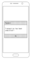
FIG. 32 is a diagram showing a user interface for performing payment executed in step S200 shown in FIG. 31 by way of example.
FIG. 33 is a diagram showing a user interface for contact executed in step S300 shown in FIG. 31 as an example.
34 and 35 exemplarily show a user interface for completing a payment executed in step S400 shown in FIG. 31 .
아래에서는, 본 발명의 기술 분야에서 통상의 지식을 가진 자가 본 발명을 용이하게 실시할 수 있을 정도로, 본 발명의 실시 예들이 명확하고 상세하게 기재될 것이다.In the following, embodiments of the present invention will be described clearly and in detail to the extent that a person skilled in the art can easily practice the present invention.
도 1은 본 발명의 실시 예에 따른 전자장치를 예시적으로 보여주는 블록도이다. 도 1을 참조하면, 전자장치(100)는 모바일 장치(110) 및 액세서리(120)를 포함할 수 있다.1 is a block diagram showing an electronic device according to an embodiment of the present invention by way of example. Referring to FIG. 1 , an
모바일 장치(110)는 휴대폰, 스마트폰, 태블릿 PC, 노트북, 디지털 카메라, 스마트 링, 또는 스마트 워치 등이 될 수 있다. 모바일 장치(110)는 NFC를 지원할 수 있다. 모바일 장치(110)는 다른 모바일 장치와 데이터의 송수신이 가능할 수 있다.The
액세서리(120)는 모바일 장치(110)의 일부 또는 전부에 부착될 수 있다. 액세서리(120)는 모바일 장치(110)와 탈부착이 가능할 수 있다. 예를 들면, 액세서리(120)는 가죽, 우레탄, 플라스틱 또는 메탈(Metal) 등으로 제조될 수 있다. 예를 들면, 액세서리(120)는 모바일 장치(110)의 일면에 완전히 부착되는 필름일 수도 있다. 예를 들면, 액세서리(120)는 커버, 스티커, 미끄럼 방지 패드, 필름, 보조배터리, 또는 스마트그립(Smart Grip) 등일 수 있다. 액세서리(120)는 상술한 내용에 한정되지 않고, 모바일 장치(110)를 보호하기 위해 다양한 형태로 제조될 수 있다. 액세서리(120)는 모바일 장치(110)의 미적 감각(Aesthetic Sense)을 향상시키기 위해 다양한 형태로 제조될 수 있다.
도 1을 참조하면, 모바일 장치(110)는 어플리케이션 프로세서(Application Processor, AP, 111), NFC 송수신기(NFC Transceiver, 112), 매칭 회로(Matching Circuit, 113), 및 단자들(114, 115)을 포함할 수 있다.Referring to FIG. 1, the
어플리케이션 프로세서(111)는 하드웨어 회로들(예를 들면, 하나 또는 그 보다 많은 프로세서들)을 포함하며, 전자장치(100)에 의해서 제공되는 다양한 사용자 응용들을 제공하도록 동작할 수 있다. 사용자 응용들은 음성 호출 동작들, 데이터 전송 등을 포함할 수 있다.The
어플리케이션 프로세서(111)는 전자장치(100)가 다른 모바일 장치와 사진, 동영상 등의 정보를 송수신할 수 있는 프로그램들을 실행할 수 있다. 어플리케이션 프로세서(111)는 전자장치(100)가 카드와 같이 동작할 수 있는 프로그램들을 실행할 수 있다. 어플리케이션 프로세서(111)는 모바일 포스(Mobile Point of Sales: mPOS)를 위한 프로그램들을 실행할 수 있다. 이러한 프로그램들은 전자장치(100)를 이용한 신용카드 구매 및 결제 기능들을 제공할 수 있다.The
NFC 송수신기(112)는 무선 통신을 위해 유도 결합(Inductive Coupling)을 이용하여 NFC 신호들을 송수신하도록 구성될 수 있다. NFC 송수신기(112)는 NFC 신호들을 매칭 회로(113)를 거쳐 안테나(130)에 제공할 수 있다. 안테나(130)는 유도 결합을 통해 NFC 신호들을 전송할 수 있다. 안테나(130)는 NFC 신호들(NFC 신호들의 송수신이 가능한 다른 전자장치(미도시)로부터 제공됨)을 수신할 수 있다. 안테나(130)는 수신된 NFC 신호들을 매칭 회로(113)를 거쳐 NFC 송수신기(112)에 제공할 수 있다.The
NFC 송수신기(112)는 NFC 인터페이스 및 프로토콜-1 (NFCIP-1)과 NFC 인터페이스 및 프로토콜-2 (NFCIP-2)에 설명되고 ECMA-340, ISO/IEC 18092, ETSI TS 102 190, ISO 21481, ECMA 352, ETSI TS 102 312 등에 표준화된 규정들과 일치하게 동작할 수 있다.The
매칭 회로(113)는 NFC 송수신기(112) 및 안테나(130)와 연결될 수 있다. 매칭 회로(113)는 전자장치(100)가 NFC를 수행하는 경우, 13.56MHz 주파수 하모닉(Harmonic) 성분을 줄이는 EMC 필터(Electromagnetic Compatibility Filter)를 포함할 수 있다. 매칭 회로(113)는 임피던스(Impedance) 매칭을 위해 커패시터(Capacitor) 등을 포함할 수 있다. 임피던스 매칭은 NFC 송수신기(112)와 안테나(130) 사이의 신호의 송수신을 위해 필요할 수 있다. 매칭 회로(113)의 상세한 구조는 도 5에서 후술한다.The
단자들(114, 115)은 매칭 회로(113)와 연결될 수 있다. 단자들(114, 115)은 후술할 액세서리의 단자들(124, 125)과 물리적 또는 전기적으로 연결될 수 있다. 예를 들면, 단자들(114, 115)은 단자들(124, 125)과 직접 연결될 수 있고 또는 와이어를 이용하여 연결될 수도 있다.
도 1을 참조하면, 액세서리(120)는 단자들(124, 125) 및 안테나(130)를 포함할 수 있다. 단자들(124, 125)은 안테나(130)와 연결될 수 있다. 단자들(124, 125)은 모바일 장치의 단자들(114, 115)과 물리적 또는 전기적으로 연결될 수 있다. 예를 들면, 단자들(124, 125)은 단자들(114, 115)과 직접 연결될 수 있고 또는 와이어를 이용하여 연결될 수도 있다.Referring to FIG. 1 ,
안테나(130)는 단자들(124, 125)과 연결될 수 있다. 안테나(130)는 단자들(114, 115, 124, 125)을 통해 매칭 회로(113)와도 연결될 수 있다. 안테나(130)는 어플리케이션 프로세서(111)에서 생성된 신호들을 NFC 송수신기(112) 및 매칭 회로(113)를 통해 전달받을 수 있다. 안테나(130)는 외부의 NFC 신호들을 전달받는데 사용될 수 있다. 안테나(130)는 다른 모바일 장치, 카드, 또는 카드 리더기 등에 NFC 신호들을 전송하기 위해 사용될 수 있다. 안테나(130)는 유도 결합에 의해 NFC 신호들의 전송 및 수신을 위해 사용될 수 있다.
도 1을 참조하면, 본 발명의 실시 예에 따른 전자장치(100)는 액세서리(120) 내에 배치되는 안테나(130)를 포함할 수 있다. 이를 통해, 안테나(130)의 배치 자유도는 향상될 수 있다.Referring to FIG. 1 , an
도 2 및 도 3은 도 1에서 도시한 안테나를 예시적으로 보여주는 도면이다. 도 2 및 도 3을 참조하면, 안테나(130)는 제 1 코일(Coil, 131) 및 제 2 코일(132)을 포함할 수 있다. 제 1 코일(131)은 단자들(124, 125)과 연결될 수 있다. 제 1 코일(131)과 제 2 코일(132)은 서로 분리되어 배치될 수 있다. 도 2를 참조하면, 제 1 코일(131) 및 제 2 코일(132)은 렉텡귤러 스파이럴(Rectangular Spiral) 형태로 구현될 수 있다. 도 3을 참조하면, 제 1 코일(131) 및 제 2 코일(132)은 헬리컬(Helical) 형태로 구현될 수 있다.2 and 3 are diagrams showing the antenna shown in FIG. 1 as an example. Referring to FIGS. 2 and 3 , the
각 코일의 길이, 두께, 폭, 위치, 또는 턴 수, 또는 코일들간의 폭은 공진주파수에 필요한 인덕턴스(Inductance) 또는 커패시턴스(Capacitance)에 의해 결정될 수 있다. 제 1 코일(131) 및 제 2 코일(132) 각각의 턴 수, 폭, 길이, 위치, 및 두께 등은 도 2 및 도 3에서 도시된 것에 한정되지 않는다. 또한 도 2 및 도 3을 참조하면, 코일들(131, 132)이 겹쳐지는 영역이 있다. 겹쳐지는 영역은 절연물질을 통해 분리될 수 있다. 예를 들면, 코일은 비아(Via, 미도시)를 통해 복수의 층들(Layers)에 배치될 수 있고, 각 층 사이에는 절연물질이 배치될 수 있다.The length, thickness, width, position, or number of turns of each coil, or the width between coils may be determined by inductance or capacitance required for a resonant frequency. The number of turns, width, length, location, and thickness of each of the
제 1 코일(131) 또는 제 2 코일(132)은 여러 재질을 이용하여 제작될 수 있다. 예를 들면, 구리나 리츠 와이어(Litz-Wire)가 사용될 수 있다. 제 1 코일(131) 및 제 2 코일(132)은 PCB(Printed Circuit Board) 또는 FPCB(Flexible Printed Circuit Board)에서 구현될 수 있다. 본 발명의 실시 예에 따른 제 1 코일(131) 또는 제 2 코일(132)은 도 2 및 도 3에 도시된 것에 한정되지 않고 다양한 형태 또는 재질로 제작될 수 있다.The
도 2 및 도 3을 참조하면, 제 2 코일(132) 양단에는 커패시터가 더 연결될 수 있다. 커패시터는 주파수 튜닝(Tuning)을 위해 제 2 코일(132)에 덧붙여질 수 있다. 도시되진 않았지만, 제 2 코일(132)이 커패시터를 포함하지 않는 경우, 제 2 코일(132)의 양단은 곧바로 연결될 수 있다. 도시되진 않았지만, 제 2 코일(132)과 마찬가지로, 제 1 코일(131)도 커패시터를 더 포함할 수 있다. 이하, 안테나(130)의 등가회로에 대해 설명한다.Referring to FIGS. 2 and 3 , a capacitor may be further connected to both ends of the
도 4는 본 발명의 실시 예에 따른 안테나의 등가회로를 예시적으로 보여주는 도면이다. 도 4는 도 2 및 도 3을 참조하여 설명될 것이다. 도 4를 참조하면, 안테나(130)는 제 1 인덕터(Inductor, L1), 제 2 인덕터(L2), 제 1 커패시터(C1), 또는 제 2 커패시터(C2)를 포함하는 등가회로로 나타낼 수 있다. 제 1 인덕터(L1)는 제 1 코일(131)의 인덕터 성분을 의미한다. 제 1 커패시터(C1)는 제 1 코일(131)의 커패시터 성분을 의미한다. 제 2 인덕터(L2)는 제 2 코일(132)의 인덕터 성분을 의미한다. 제 2 커패시터(C2)는 제 2 코일(132)의 커패시터 성분을 의미한다.4 is a diagram exemplarily showing an equivalent circuit of an antenna according to an embodiment of the present invention. FIG. 4 will be described with reference to FIGS. 2 and 3 . Referring to FIG. 4 , the
제 1 인덕터(L1)와 제 1 커패시터(C1)는 병렬 공진기를 구성할 수 있다. 제 2 인덕터(L2)와 제 2 커패시터(C2)는 병렬 공진기를 구성할 수 있다. 각 인덕터는 각 코일의 형태, 두께, 또는 배치되는 공간 등에 따라 결정될 수 있다. 각 커패시터는 기생(Parasitic) 커패시터 또는 집중정수 소자(Lumped Element)일 수 있다. 각 커패시터가 집중정수 소자인 경우, 제 1 코일(131) 및 제 2 코일(132) 각각은 양단에 커패시터들을 추가로 더 포함할 수 있다.The first inductor L1 and the first capacitor C1 may form a parallel resonator. The second inductor L2 and the second capacitor C2 may constitute a parallel resonator. Each inductor may be determined according to the shape, thickness, or space of each coil. Each capacitor may be a parasitic capacitor or a lumped element. When each capacitor is a lumped constant element, each of the
도 4를 참조하면, 각 인덕터와 각 커패시터는 병렬로 연결될 수 있다. 도시되진 않았지만, 각 인덕터와 각 커패시터는 직렬로 연결될 수도 있다. 도시되진 않았지만, 제 1 코일(131) 및 제 2 코일(132)은 각각 레지스터(Resistor)를 더 포함할 수도 있다.Referring to FIG. 4 , each inductor and each capacitor may be connected in parallel. Although not shown, each inductor and each capacitor may be connected in series. Although not shown, each of the
전자장치(100)가 NFC 신호들을 전송하는 경우, 제 1 인덕터(L1)에 흐르는 전류로 인하여, 제 1 인덕터(L1) 주변에 자기장이 형성될 수 있다. 형성된 자기장에 의하여 제 2 인덕터(L2)에 유도 전류가 흐를 수 있다. 즉, 제 2 인덕터(L2)는 자기 유도(Magnetic Induction)에 의해 제 1 인덕터(L1)로부터 전력을 공급받을 수 있다. 제 2 인덕터(L2)와 제 2 커패시터(C2)는 상술한 전력에 의해서, NFC 신호에 의해 점유되는 주파수들의 밴드 중 중심 주파수(예를 들면, 13.56MHz)에서 공진될 수 있다.When the
전자장치(100)가 NFC 신호들을 수신하는 경우, 제 2 인덕터(L2)와 제 2 커패시터(C2)로 이루어진 병렬 공진기는 외부 장치에서 전송된 NFC 신호에 의해 공진될 수 있다. 제 1 인덕터(L1)는 자기 유도에 의해 제 2 인덕터(L2)로부터 전력을 공급받을 수 있다. 제 1 인덕터(L1)와 제 1 커패시터(C1)는 상술한 전력에 의해 공진될 수 있다. NFC 신호들은 매칭 회로(113) 및 NFC 송수신기(112)를 거쳐 어플리케이션 프로세서(111)로 전달될 수 있다.When the
도 4에 도시된 바와 같이, 제 1 인덕터(L1)와 제 2 인덕터(L2)는 NFC 신호들의 송수신을 위해 분리되어 배치될 수 있다. 제 1 인덕터(L1)와 제 2 인덕터(L2)가 분리되어 있어, 양자간에 전자기 유도(Inductive Coupling) 현상이 발생될 수 있다. 제 1 인덕터(L1)와 제 2 인덕터(L2)가 분리되어 있어, 전자장치(100)는 NFC 신호들의 송수신 성능(Quality Factor)을 향상시킬 수 있다. 도시되진 않았지만, 안테나(130)는 제 1 코일(도 2 및 도 3 참조, 131)만을 포함할 수 있다. 안테나(130)는 제 1 코일(도 2 및 도 3 참조, 131)에 더해 제 2 코일(도 2 및 도 3 참조, 132)도 포함할 수 있다. 즉, 안테나(130)의 송수신 성능 향상을 위해, 안테나(130)는 제 2 코일(도 2 및 도 3 참조, 132)을 더 포함할 수 있다.As shown in FIG. 4 , the first inductor L1 and the second inductor L2 may be separately disposed for transmitting and receiving NFC signals. Since the first inductor L1 and the second inductor L2 are separated, an electromagnetic induction phenomenon may occur between them. Since the first inductor L1 and the second inductor L2 are separated, the
안테나 사이즈(또는, 안테나가 형성되는 영역)는 용도 또는 목적에 따라 변경될 수 있다. 예를 들면, 신용카드 결제를 위한 mPOS 방식에 사용되는 안테나 사이즈는 데이터 통신을 위한 P2P 방식에 사용되는 안테나 사이즈와 다를 수 있다.The size of the antenna (or the area where the antenna is formed) may be changed according to the use or purpose. For example, the antenna size used in the mPOS method for credit card payment may be different from the antenna size used in the P2P method for data communication.
본 발명의 실시 예에 따른 전자장치(100)는 액세서리(120) 내부에 배치되는 안테나(130)를 포함할 수 있다. 즉, 제 1 코일(131) 및 제 2 코일(132)은 액세서리(120) 내부에 배치될 수 있다. 이를 통해, 안테나(130)의 배치 자유도는 향상될 수 있다. 본 발명의 실시 예에 따른 전자장치(100)는 안테나(130)를 액세서리(120)에 배치함으로써, NFC의 P2P 모드, 리더 모드, 카드 에뮬레이션 모드들을 지원할 수 있다.The
도 5는 본 발명의 실시 예에 따른 매칭 회로를 예시적으로 보여주는 도면이다. 도 5를 참조하면, 매칭 회로(113)는 인덕터들(L7, L8) 및 커패시터들(C7, C8, C9, C10)을 포함할 수 있다. 인덕터들(L7, L8)과 커패시터들(C7, C8)은 EMC 필터(Electromagnetic Compatibility Filter)로 구성할 수 있다. EMC 필터 (Electromagnetic Compatibility Filter)는 NFC 신호들의 13.56MHz 주파수의 하모닉(Harmonic) 성분을 줄일 수 있다. 인덕터들(L7, L8)과 커패시터들(C7, C8)의 크기들은 하모닉 성분을 고려하여 결정될 수 있다.5 is a diagram showing a matching circuit according to an embodiment of the present invention by way of example. Referring to FIG. 5 , the
커패시터들(C9, C10)은 임피던스 매칭을 위해 사용될 수 있다. 커패시터들(C9, C10)의 크기는 NFC 송수신기(112), 단자들(114, 115, 124, 125), 또는 안테나(130)의 각 부하를 고려하여 결정될 수 있다. 커패시터들(C7, C8)과 인덕터들(L7, L8)의 크기는 커패시터들(C9, C10)과 NFC 송수신기(112)의 각 부하를 고려하여 결정될 수 있다.Capacitors C9 and C10 may be used for impedance matching. The size of the capacitors C9 and C10 may be determined considering each load of the
도 6은 본 발명의 실시 예에 따른 전자장치를 예시적으로 보여주는 블록도이다. 도 6은 도 1을 참조하여 설명될 것이다. 도 6을 참조하면, 전자장치(200)는 모바일 장치(210) 또는 액세서리(220)를 포함할 수 있다. 전자장치(200)의 모바일 장치(210) 및 액세서리(220)는 앞서 설명한 전자장치(100)의 모바일 장치(110) 및 액세서리(120)와 각각 동일한 기능을 수행할 수 있다.6 is a block diagram showing an electronic device according to an embodiment of the present invention by way of example. FIG. 6 will be described with reference to FIG. 1 . Referring to FIG. 6 , the
도 6을 참조하면, 모바일 장치(210)는 어플리케이션 프로세서(211), NFC 송수신기(212), 및 매칭 회로(213)를 포함할 수 있다. 모바일 장치(210)의 어플리케이션 프로세서(211), NFC 송수신기(212), 및 매칭 회로(213)는 앞서 설명한 모바일 장치(110)의 어플리케이션 프로세서(111), NFC 송수신기(112), 및 매칭 회로(113)와 각각 동일한 기능을 수행하므로 이에 대한 설명은 생략하기로 한다. 도 6을 참조하면, 도 1에서 도시된 안테나(130)는 액세서리(120)에 배치된 것과 달리, 안테나(230)는 모바일 장치(210) 및 액세서리(220)에 배치될 수 있다. 예를 들면, 안테나(230)는 복수의 코일들로 구성될 수 있다. 안테나(230)의 일부 코일들은 모바일 장치(210)에 배치될 수 있고, 안테나(230)의 나머지 코일들은 액세서리(220)에 배치될 수 있다.Referring to FIG. 6 , a
도 7 내지 도 13은 도 6에서 도시한 안테나를 예시적으로 보여주는 도면이다. 도 7 및 도 8을 참조하면, 안테나(230)는 제 1 코일(231) 및 제 2 코일(232)을 포함할 수 있다. 제 1 코일(231)은 모바일 장치(210)에 배치될 수 있다. 제 2 코일(232)은 액세서리(220)에 배치될 수 있다. 제 1 코일(231) 및 제 2 코일(232)은 서로 분리되어 배치될 수 있다. 도 7을 참조하면, 제 1 코일(231) 및 제 2 코일(232)은 렉텡귤러 스파이럴 형태로 구현될 수 있다. 도 8를 참조하면, 제 1 코일(231) 및 제 2 코일(232)은 헬리컬 형태로 구현될 수 있다. 제 1 코일(231) 및 제 2 코일(232) 각각의 턴 수, 폭, 길이, 위치, 및 두께 등은 도 7 및 도 8에서 도시된 것에 한정되지 않는다. 또한 도 7 내지 도 13을 참조하면, 코일들(231, 232)이 겹쳐지는 영역이 있고, 제 3 코일(233)과 제 2 코일(232)에 겹쳐지는 영역이 있다. 겹쳐지는 영역은 절연물질을 통해 분리될 수 있다. 예를 들면, 코일은 비아(Via, 미도시)를 통해 복수의 층들(Layers)에 배치될 수 있고, 각 층 사이에는 절연물질이 배치될 수 있다.도 7 및 도 8을 참조하면, 제 2 코일(232) 양단에는 커패시터가 더 연결될 수 있다. 커패시터는 주파수 튜닝을 위해 제 2 코일(232)에 덧붙여질 수 있다. 도시되진 않았지만, 제 2 코일(232)이 커패시터를 포함하지 않는 경우, 제 2 코일(232)의 양단은 곧바로 연결될 수 있다. 도시되진 않았지만, 제 2 코일(232)과 마찬가지로, 제 1 코일(231)도 커패시터를 더 포함할 수 있다.7 to 13 are diagrams showing the antenna shown in FIG. 6 by way of example. Referring to FIGS. 7 and 8 , the
도 7 및 도 8을 참조하면, 모바일 장치(210)와 액세서리(220) 사이의 거리는 d1이다. 제 1 코일(231)과 제 2 코일(232) 사이의 거리는 d2이다. 도 9는 모바일 장치(210)와 액세서리(220) 사이의 거리(d1) 및 제 1 코일(231)과 제 2 코일(232) 사이의 거리(d2)를 이해하기 쉽게 나타낸 도면이다. d1, d2는 제 1 코일(231)의 인덕터와 제 2 코일(232)의 인덕터 사이에 전자기 유도 현상을 일으키기 위해 적절하게 설정될 수 있다. 예를 들면, d1은 5mm 이하일 수 있다. 예를 들면, d2는 10mm 이하일 수 있다.Referring to FIGS. 7 and 8 , the distance between the
제 1 코일(231) 및 제 2 코일(232)은 앞서 서술한 제 1 코일(131) 및 제 2 코일(132)과 배치되는 위치만 상이하고 각각 동일한 기능을 수행하므로 이에 대한 상세한 설명은 생략하기로 한다.Since the
도 10 및 도 11을 참조하면, 안테나(230)는 제 1 코일(231), 제 2 코일(232), 및 제 3 코일(233)을 포함할 수 있다. 제 1 코일(231)은 모바일 장치(210)에 배치될 수 있다. 제 2 코일(232) 및 제 3 코일(233)은 액세서리(220)에 배치될 수 있다 도 7 및 도 8과 비교하여, NFC 신호들의 송수신 성능을 높이기 위해, 안테나(230)는 제 2 코일(232)과 분리된 제 3 코일(233)을 더 포함할 수 있다. 제 3 코일(233)의 인덕터에도 제 2 코일(232)의 인덕터 및 제 1 코일(231)의 인덕터와 같이 자기 유도 현상이 발생될 수 있다. 도 10을 참조하면, 제 3 코일(233)은 렉텡귤러 스파이럴 형태로 구현될 수 있다. 도 11을 참조하면, 제 3 코일(233)은 헬리컬 형태로 구현될 수 있다. 제 3 코일(233)의 턴 수, 폭, 길이, 위치, 및 두께 등은 도 10 및 도 11에서 도시된 것에 한정되지 않는다. Referring to FIGS. 10 and 11 , the
도 10 및 도 11을 참조하면, 제 3 코일(233) 양단에는 커패시터가 더 연결될 수 있다. 커패시터는 주파수 튜닝을 위해 제 3 코일(233)에 덧붙여질 수 있다. 도시되진 않았지만, 제 3 코일(233)이 커패시터를 포함하지 않는 경우, 제 3 코일(233)의 양단은 곧바로 연결될 수 있다. 제 1 코일(231) 및 제 2 코일(232)은 앞서 서술한 제 1 코일(131) 및 제 2 코일(132)과 배치되는 위치만 상이하고 각각 동일한 기능을 수행하므로 이에 대한 상세한 설명은 생략하기로 한다. 제 3 코일(233)은 제 2 코일(232)과 분리되어 배치될 수 있다. 제 3 코일(233)은 제 2 코일(232)과 배치되는 위치만 상이하고 동일한 기능을 수행하므로 이에 대한 상세한 설명은 생략하기로 한다.Referring to FIGS. 10 and 11 , a capacitor may be further connected to both ends of the
도 10 및 도 11을 참조하면, 모바일 장치(210)와 액세서리(220) 사이의 거리는 d1이다. 제 1 코일(231)과 제 2 코일(232) 사이의 거리는 d2이다. d1, d2는 제 1 코일(231)의 인덕터와 제 2 코일(232)의 인덕터 사이에 전자기 유도 현상을 일으키기 위해 적절하게 설정될 수 있다. 예를 들면, d1은 5mm 이하일 수 있다. 예를 들면, d2는 10mm 이하일 수 있다.Referring to FIGS. 10 and 11 , the distance between the
도 12 및 도 13을 참조하면, 안테나(230)는 제 1 코일(231), 제 2 코일(232), 제 3 코일(233), 및 제 4 코일(234)을 포함할 수 있다. 제 1 코일(231)은 모바일 장치(210)에 배치될 수 있다. 제 2 코일(232), 제 3 코일(233), 및 제 4 코일(234)은 액세서리(220)에 배치될 수 있다. 이 경우, 액세서리(220)는 모바일 장치(210)의 플립 커버일 수 있다. 도 10 및 도 11과 비교하여, NFC 신호들의 송수신 성능을 높이기 위해, 안테나(230)는 제 3 코일(233)과 연결된 제 4 코일(234)을 더 포함할 수 있다. 도시되진 않았지만, 제 4 코일(234)는 제 3 코일(233)과 연결되지 않을 수도 있다. 플립 커버가 닫히는 경우, 제 4 코일(234)의 인덕터에도 제 3 코일(233), 제 2 코일(232), 및 제 1 코일(231)의 인덕터와 같이 전자기 유도 현상이 발생될 수 있다. 도 12를 참조하면, 제 4 코일(234)은 렉텡귤러 스파이럴 형태로 구현될 수 있다. 도 13을 참조하면, 제 4 코일(234)은 헬리컬 형태로 구현될 수 있다. 제 4 코일(234)의 턴 수, 폭, 길이, 위치, 및 두께 등은 도 12 및 도 13에서 도시된 것에 한정되지 않는다. Referring to FIGS. 12 and 13 , the
도 12 및 도 13을 참조하면, 제 4 코일(234) 양단에는 커패시터가 더 연결될 수 있다. 커패시터는 주파수 튜닝을 위해 제 4 코일(234)에 덧붙여질 수 있다. 도시되진 않았지만, 제 4 코일(234)이 커패시터를 포함하지 않는 경우, 제 4 코일(234)의 양단은 곧바로 연결될 수 있다.Referring to FIGS. 12 and 13 , a capacitor may be further connected to both ends of the
제 1 코일(231), 제 2 코일(232), 및 제 3 코일(233)은 도 10 및 도 11에서 서술한 제 1 코일(231), 제 2 코일(232), 및 제 3 코일(233)과 각각 동일한 기능을 수행하므로 이에 대한 상세한 설명은 생략하기로 한다. 제 3 코일(233)은 플립커버 후면에 배치될 수 있다. 제 4 코일(234)은 제 3 코일(233)과 연결되어 플립커버 전면에 배치될 수 있다. 제 4 코일(234)은 제 3 코일(233)과 배치되는 위치만 상이하고 동일한 기능을 수행하므로 이에 대한 상세한 설명은 생략하기로 한다.The
도 12 및 도 13을 참조하면, 제 2 코일(232) 및 제 3 코일(233)은 플립커버 후면에 배치될 수 있고, 제 4 코일(234)은 플립커버 전면에 배치될 수 있다. 도시되진 않았으나, 제 2 코일(232), 제 3 코일(233), 및 제 4 코일(234)은 모두 플립커버 전면 또는 플립커버 후면에 배치될 수도 있다. 도시되진 않았으나, 제 2 코일(232) 및 제 3 코일(233)은 플립커버 전면에 배치될 수 있고, 제 4 코일(234)은 플립커버 후면에 배치될 수도 있다.Referring to FIGS. 12 and 13 , the
도 12 및 도 13을 참조하면, 모바일 장치(210)와 액세서리(220) 사이의 거리는 d1이다. 제 1 코일(231)과 제 2 코일(232) 사이의 거리는 d2이다. d1, d2는 제 1 코일(231)의 인덕터와 제 2 코일(232)의 인덕터 사이에 전자기 유도 현상을 일으키기 위해 적절하게 설정될 수 있다. 예를 들면, d1은 5mm 이하일 수 있다. 예를 들면, d2는 10mm 이하일 수 있다.Referring to FIGS. 12 and 13 , the distance between the
도 7 내지 도 13을 참조하면, 모바일 장치(210)는 휴대폰, 스마트폰, 태블릿 PC, 노트북, 디지털 카메라, 스마트 링, 또는 스마트 워치 등이 될 수 있다. 액세서리(220)는 모바일 장치(210)의 일부 또는 전부에 부착될 수 있다. 액세서리(220)는 모바일 장치(210)와 탈부착이 가능할 수 있다. 예를 들면, 액세서리(220)는 가죽, 우레탄, 플라스틱 또는 메탈(Metal) 등으로 제조될 수 있다. 예를 들면, 액세서리(220)는 모바일 장치(210)의 일면에 완전히 부착되는 필름일 수도 있다. 예를 들면, 액세서리(220)는 커버, 스티커, 미끄럼 방지 패드, 필름, 보조배터리, 또는 스마트그립 등일 수 있다. 액세서리(220)는 상술한 내용에 한정되지 않고, 모바일 장치(210)를 보호하기 위해 다양한 형태로 제조될 수 있다. 액세서리(220)는 모바일 장치(210)의 미적 감각을 향상시키기 위해 다양한 형태로 제조될 수 있다.Referring to FIGS. 7 to 13 , the
도 7 내지 도 13을 참조하면, 코일들(231, 232, 233, 234)은 모바일 장치(210) 또는 액세서리(220)의 중앙에 배치될 수 있고, 렉텡귤러 스파이럴 형태 또는 헬리컬 형태로 구현될 수 있지만, 본 발명은 여기에 제한되지 않을 것이다. 즉, 코일들(231, 232, 233, 234)은 모바일 장치(210) 또는 액세서리(220)의 모든 공간을 활용하여 배치될 수도 있다. 상술한 공간에서 코일들(231, 232, 233, 234)은 루프(Loop)를 형성하는 모든 형태로 구현될 수 있다.7 to 13, the
도 14는 도 7 및 도 8에서 도시된 본 발명의 실시 예에 따른 안테나의 등가회로를 예시적으로 보여주는 도면이다. 도 14는 도 7 및 도 8을 참조하여 설명될 것이다. 도 14를 참조하면, 안테나(230)는 제 1 인덕터(L3), 제 2 인덕터(L4), 제 1 커패시터(C3), 또는 제 2 커패시터(C4)를 포함하는 등가회로로 나타낼 수 있다. 제 1 인덕터(L3)는 제 1 코일(231)의 인덕터 성분을 의미한다. 제 1 커패시터(C3)는 제 1 코일(231)의 커패시터 성분을 의미한다. 제 2 인덕터(L4)는 제 2 코일(232)의 인덕터 성분을 의미한다. 제 2 커패시터(C4)는 제 2 코일(232)의 커패시터 성분을 의미한다.14 is a diagram showing an equivalent circuit of the antenna according to the embodiment of the present invention shown in FIGS. 7 and 8 by way of example. 14 will be described with reference to FIGS. 7 and 8 . Referring to FIG. 14 , the
제 1 인덕터(L3)와 제 1 커패시터(C3)는 병렬 공진기를 구성할 수 있다. 제 2 인덕터(L4)와 제 2 커패시터(C4)는 병렬 공진기를 구성할 수 있다. 각 인덕터는 각 코일의 형태, 두께, 또는 배치되는 공간 등에 따라 결정될 수 있다. 각 커패시터는 기생(Parasitic) 커패시터 또는 집중정수 소자(Lumped Element)일 수 있다. 각 커패시터가 집중정수 소자인 경우, 제 1 코일(231) 및 제 2 코일(232) 각각은 커패시터들을 추가로 더 포함할 수 있다.The first inductor L3 and the first capacitor C3 may constitute a parallel resonator. The second inductor L4 and the second capacitor C4 may constitute a parallel resonator. Each inductor may be determined according to the shape, thickness, or space of each coil. Each capacitor may be a parasitic capacitor or a lumped element. When each capacitor is a lumped constant element, each of the
도 14를 참조하면, 각 인덕터와 각 커패시터는 병렬로 연결될 수 있다. 도시되진 않았지만, 각 인덕터와 각 커패시터는 직렬로 연결될 수 있다. 도시되진 않았지만, 제 1 코일(231) 및 제 2 코일(232)은 각각 레지스터를 더 포함할 수도 있다.Referring to FIG. 14 , each inductor and each capacitor may be connected in parallel. Although not shown, each inductor and each capacitor may be connected in series. Although not shown, each of the
전자장치(200)가 NFC 신호들을 전송하는 경우, 제 1 인덕터(L3)에 흐르는 전류로 인하여, 제 1 인덕터(L3) 주변에 자기장이 형성될 수 있다. 형성된 자기장에 의하여 제 2 인덕터(L4)에는 유도 전류가 흐를 수 있다. 즉, 제 2 인덕터(L4)는 자기 유도(Magnetic Induction)에 의해 제 1 인덕터(L3)로부터 전력을 공급받을 수 있다. 제 2 인덕터(L4)와 제 2 커패시터(C4)는 상술한 전력에 의해서, NFC 신호에 의해 점유되는 주파수들의 밴드 중 중심 주파수(예를 들면, 13.56MHz)에서 공진될 수 있다.When the
전자장치(200)가 NFC 신호들을 수신하는 경우, 제 2 인덕터(L4)와 제 2 커패시터(C4)로 이루어진 병렬 공진기는 외부 장치에서 전송된 NFC 신호에 의해 공진될 수 있다. 제 1 인덕터(L3)는 자기 유도에 의해 제 2 인덕터(L4)로부터 전력을 공급받을 수 있다. 제 1 인덕터(L3)와 제 1 커패시터(C3)는 상술한 전력에 의해 공진될 수 있다. NFC 신호들은 매칭 회로(213) 및 NFC 송수신기(212)를 거쳐 어플리케이션 프로세서(211)로 전달될 수 있다.When the
도 14에 도시된 바와 같이, 제 1 인덕터(L3)와 제 2 인덕터(L4)는 NFC 신호들의 송수신을 위해 분리되어 배치될 수 있다. 제 1 인덕터(L3)와 제 2 인덕터(L4)가 분리되어 있어, 양자간에 전자기 유도 현상이 발생될 수 있다. 제 1 인덕터(L3)와 제 2 인덕터(L4)가 분리되어 있어, 전자장치(200)는 NFC 신호들의 송수신 성능을 향상시킬 수 있다. 도시되진 않았지만, 안테나(230)는 제 1 코일(도 7 및 도 8 참조, 231)만을 포함할 수 있다. 안테나(230)는 제 1 코일(도 7 및 도 8 참조, 231)에 더해 제 2 코일(도 7 및 도 8 참조, 232)도 포함할 수 있다. 즉, 제 1 코일(도 7 및 도 8 참조, 231) 및 제 2 코일(도 7 및 도 8 참조, 232) 사이의 전자기 유도 현상을 통해, 안테나(230)의 송수신 성능이 향상될 수 있다.As shown in FIG. 14 , the first inductor L3 and the second inductor L4 may be disposed separately for transmission and reception of NFC signals. Since the first inductor L3 and the second inductor L4 are separated, an electromagnetic induction phenomenon may occur between them. Since the first inductor L3 and the second inductor L4 are separated, the
도 15는 도 10 및 도 11에서 도시된 본 발명의 실시 예에 따른 안테나의 등가회로를 예시적으로 보여주는 도면이다. 도 15는 도 10 및 도 11을 참조하여 설명될 것이다. 도 15를 참조하면, 안테나(230)는 제 1 인덕터(L3), 제 2 인덕터(L4), 제 3 인덕터(L5), 제 1 커패시터(C3), 제 2 커패시터(C4), 또는 제 3 커패시터(C5)를 포함하는 등가회로로 나타낼 수 있다. 제 1 인덕터(L3), 제 2 인덕터(L4), 제 1 커패시터(C3), 및 제 2 커패시터(C4) 각각은 도 14에서 상술한 것과 동일한 기능을 수행하므로 이에 대한 설명은 생략하기로 한다.15 is a diagram showing an equivalent circuit of the antenna according to the embodiment of the present invention shown in FIGS. 10 and 11 by way of example. 15 will be described with reference to FIGS. 10 and 11 . Referring to FIG. 15, the
도 15를 참조하면, 제 3 인덕터(L5)는 제 3 코일(도 10 및 도 11 참조, 233)의 인덕터 성분을 의미한다. 제 3 커패시터(C5)는 제 3 코일(도 10 및 도 11 참조, 233)의 커패시터 성분을 의미한다. 제 3 인덕터(L5)와 제 3 커패시터(C5)는 병렬 공진기를 구성할 수 있다. 제 3 커패시터가 집중정수 소자인 경우, 안테나(230)는 제 3 코일(도 10 및 도 11 참조, 233)에 연결된 커패시터들을 추가로 더 포함할 수 있다. 도시되진 않았지만, 제 3 인덕터(L5)와 제 3 커패시터(C5)는 직렬로 연결될 수 있다. 도시되진 않았지만, 제 3 코일(도 10 및 도 11 참조, 233)은 레지스터를 더 포함할 수도 있다.Referring to FIG. 15 , the third inductor L5 means an inductor component of the third coil (refer to FIGS. 10 and 11 , 233 ). The third capacitor C5 means a capacitor component of the third coil (see FIGS. 10 and 11, 233). The third inductor L5 and the third capacitor C5 may form a parallel resonator. When the third capacitor is a lumped constant element, the
전자장치(200)가 NFC 신호들을 전송하는 경우, 제 1 인덕터(L3)에 흐르는 전류로 인하여, 제 1 인덕터(L3) 주변에 자기장이 형성될 수 있다. 형성된 자기장에 의하여 제 2 인덕터(L4) 및 제 3 인덕터(L5)에는 유도 전류가 흐를 수 있다. 즉, 제 2 인덕터(L4) 및 제 3 인덕터(L5)는 자기 유도(Magnetic Induction)에 의해 제 1 인덕터(L3)로부터 전력을 공급받을 수 있다. 제 2 인덕터(L4)와 제 2 커패시터(C4)는 상술한 전력에 의해서, NFC 신호에 의해 점유되는 주파수들의 밴드 중 중심 주파수(예를 들면, 13.56MHz)에서 공진될 수 있다. 제 3 인덕터(L5)와 제 3 커패시터(C5)는 상술한 전력에 의해서, NFC 신호에 의해 점유되는 주파수들의 밴드 중 중심 주파수(예를 들면, 13.56MHz)에서 공진될 수 있다.When the
전자장치(200)가 NFC 신호들을 수신하는 경우, 제 2 인덕터(L4)와 제 2 커패시터(C4)로 이루어진 병렬 공진기는 외부 장치에서 전송된 NFC 신호에 의해 공진될 수 있다. 전자장치(200)가 NFC 신호들을 수신하는 경우, 제 3 인덕터(L5)와 제 3 커패시터(C5)로 이루어진 병렬 공진기는 외부 장치에서 전송된 NFC 신호에 의해 공진될 수 있다. 제 1 인덕터(L3)는 자기 유도에 의해 제 2 인덕터(L4) 및 제 3 인덕터(L5)로부터 전력을 공급받을 수 있다. 제 1 인덕터(L3)와 제 1 커패시터(C3)는 상술한 전력에 의해 공진될 수 있다. NFC 신호들은 매칭 회로(213) 및 NFC 송수신기(212)를 거쳐 어플리케이션 프로세서(211)로 전달될 수 있다. When the
도 15에 도시된 바와 같이, 제 1 인덕터(L3), 제 2 인덕터(L4), 및 제 3 인덕터(L5) 각각은 NFC 신호들의 송수신을 위해 분리되어 배치될 수 있다. 제 1 인덕터(L3), 제 2 인덕터(L4), 및 제 3 인덕터(L5) 각각은 분리되어 있어, 전자장치(200)는 NFC 신호들의 송수신 성능을 향상시킬 수 있다. 도시되진 않았지만, 안테나(230)는 제 1 코일(도 10 및 도 11 참조, 231)만을 포함할 수 있다. 안테나(230)는 제 1 코일(도 10 및 도 11 참조, 231)에 더해 제 2 코일(도 10 및 도 11 참조, 232) 및 제 3 코일(도 10 및 도 11 참조, 233)도 포함할 수 있다. 즉, 안테나(230)의 송수신 성능 향상을 위해, 안테나(230)는 제 2 코일(도 10 및 도 11 참조, 232) 및 제 3 코일(도 10 및 도 11 참조, 233)을 더 포함할 수 있다.As shown in FIG. 15 , each of the first inductor L3, the second inductor L4, and the third inductor L5 may be separately disposed for transmitting and receiving NFC signals. Since the first inductor L3, the second inductor L4, and the third inductor L5 are separated from each other, the
도 16은 도 12 및 도 13에서 도시된 본 발명의 실시 예에 따른 안테나의 등가회로를 예시적으로 보여주는 도면이다. 도 16은 도 12 및 도 13을 참조하여 설명될 것이다. 도 16을 참조하면, 안테나(230)의 등가회로는 제 1 인덕터(L3), 제 2 인덕터(L4), 제 3 인덕터(L5), 제 4 인덕터(L6), 제 1 커패시터(C3), 제 2 커패시터(C4), 제 3 커패시터(C5), 또는 제 4 커패시터(C6)를 포함할 수 있다. 제 1 인덕터(L3), 제 2 인덕터(L4), 제 1 커패시터(C3), 및 제 2 커패시터(C4) 각각은 도 14에서 상술한 것과 동일한 기능을 수행하므로 이에 대한 설명은 생략하기로 한다. 제 3 인덕터(L5) 및 제 3 커패시터(C5) 각각은 도 15에서 상술한 것과 동일한 기능을 수행하므로 이에 대한 설명은 생략하기로 한다.16 is a diagram showing an equivalent circuit of the antenna according to the embodiment of the present invention shown in FIGS. 12 and 13 by way of example. 16 will be described with reference to FIGS. 12 and 13 . Referring to FIG. 16, the equivalent circuit of the
도 16을 참조하면, 제 4 인덕터(L6)는 제 4 코일(도 12 및 도 13 참조, 234)의 인덕터 성분을 의미한다. 제 4 커패시터(C6)는 제 4 코일(도 12 및 도 13 참조, 234)의 커패시터 성분을 의미한다. 제 4 인덕터(L6)와 제 4 커패시터(C6)는 병렬 공진기를 구성할 수 있다. 제 4 커패시터가 집중정수 소자인 경우, 안테나(230)는 제 4 코일(도 12 및 도 13 참조, 234)에 연결된 커패시터들을 추가로 더 포함할 수 있다. 도시되진 않았지만, 제 4 인덕터(L6)와 제 4 커패시터(C6)는 직렬로 연결될 수 있다. 도시되진 않았지만, 제 4 코일(도 12 및 도 13 참조, 234)은 레지스터를 더 포함할 수도 있다.Referring to FIG. 16 , the fourth inductor L6 means an inductor component of the fourth coil (see FIGS. 12 and 13 , 234 ). The fourth capacitor C6 means a capacitor component of the fourth coil (see FIGS. 12 and 13, 234). The fourth inductor L6 and the fourth capacitor C6 may form a parallel resonator. When the fourth capacitor is a lumped constant element, the
전자장치(200)가 NFC 신호들을 전송하는 경우, 제 1 인덕터(L3)에 흐르는 전류로 인하여, 제 1 인덕터(L3) 주변에 자기장이 형성될 수 있다. 형성된 자기장에 의하여 제 2 인덕터(L4), 제 3 인덕터(L5), 및 제 4 인덕터(L6)에는 유도 전류가 흐를 수 있다. 즉, 제 2 인덕터(L4), 제 3 인덕터(L5), 및 제 4 인덕터(L6)는 자기 유도(Magnetic Induction)에 의해 제 1 인덕터(L3)로부터 전력을 공급받을 수 있다. 제 2 인덕터(L4)와 제 2 커패시터(C4)는 상술한 전력에 의해서, NFC 신호에 의해 점유되는 주파수들의 밴드 중 중심 주파수(예를 들면, 13.56MHz)에서 공진될 수 있다. 제 3 인덕터(L5)와 제 3 커패시터(C5)는 상술한 전력에 의해서, NFC 신호에 의해 점유되는 주파수들의 밴드 중 중심 주파수(예를 들면, 13.56MHz)에서 공진될 수 있다. 제 4 인덕터(L6)와 제 4 커패시터(C6)는 상술한 전력에 의해서, NFC 신호에 의해 점유되는 주파수들의 밴드 중 중심 주파수(예를 들면, 13.56MHz)에서 공진될 수 있다.When the
전자장치(200)가 NFC 신호들을 수신하는 경우, 제 2 인덕터(L4)와 제 2 커패시터(C4)로 이루어진 병렬 공진기는 외부 장치에서 전송된 NFC 신호에 의해 공진될 수 있다. 전자장치(200)가 NFC 신호들을 수신하는 경우, 제 3 인덕터(L5)와 제 3 커패시터(C5)로 이루어진 병렬 공진기는 외부 장치에서 전송된 NFC 신호에 의해 공진될 수 있다. 전자장치(200)가 NFC 신호들을 수신하는 경우, 제 4 인덕터(L6)와 제 4 커패시터(C6)로 이루어진 병렬 공진기는 외부 장치에서 전송된 NFC 신호에 의해 공진될 수 있다. 제 1 인덕터(L3)는 자기 유도에 의해 제 2 인덕터(L4), 제 3 인덕터(L5), 및 제 4 인덕터(L6)로부터 전력을 공급받을 수 있다. 제 1 인덕터(L3)와 제 1 커패시터(C3)는 상술한 전력에 의해 공진될 수 있다. NFC 신호들은 매칭 회로(213) 및 NFC 송수신기(212)를 거쳐 어플리케이션 프로세서(211)로 전달될 수 있다. When the
도 16에 도시된 바와 같이, 제 1 인덕터(L3), 제 2 인덕터(L4), 제 3 인덕터(L5), 및 제 4 인덕터(L6) 각각은 NFC 신호들의 송수신을 위해 분리되어 배치될 수 있다. 제 1 인덕터(L3), 제 2 인덕터(L4), 제 3 인덕터(L5), 및 제 4 인덕터(L6) 각각은 분리되어 있어, 전자장치(200)는 NFC 신호들의 송수신 성능을 향상시킬 수 있다. 도시되진 않았지만, 안테나(230)는 제 1 코일(도 12 및 도 13 참조, 231)만을 포함할 수 있다. 안테나(230)는 제 1 코일(도 12 및 도 13 참조, 231)에 더해 제 2 코일(도 12 및 도 13 참조, 232), 제 3 코일(도 12 및 도 13 참조, 233), 및 제 4 코일(도 12 및 도 13 참조, 234)도 포함할 수 있다. 즉, 안테나(230)의 송수신 성능 향상을 위해, 안테나(230)는 제 2 코일(도 12 및 도 13 참조, 232), 제 3 코일(도 12 및 도 13 참조, 233), 및 제 4 코일(도 12 및 도 13 참조, 234)을 더 포함할 수 있다.As shown in FIG. 16, each of the first inductor L3, the second inductor L4, the third inductor L5, and the fourth inductor L6 may be separately disposed for transmitting and receiving NFC signals. . Since each of the first inductor L3, the second inductor L4, the third inductor L5, and the fourth inductor L6 are separated, the
본 발명의 실시 예에 따른 액세서리(220)의 내부에는 안테나(230)를 구성하는 코일들의 일부가 배치될 수 있다. 즉, 액세서리(220)의 내부에는 제 2 코일(232), 제 3 코일(233), 또는 제 4 코일(234)이 배치될 수 있다. 이를 통해, 안테나(230)의 배치 자유도가 증가될 수 있다. 본 발명의 실시 예에 따른 전자장치(200)는 안테나(230)의 일부를 액세서리(220)에 배치함으로써, NFC의 P2P 모드, 리더 모드, 카드 에뮬레이션 모드들을 지원할 수 있다.Some of the coils constituting the
다시 도 6 및 도 1을 참조하면, 도 1의 전자장치(100)와 달리, 전자장치(200)는 모바일 장치(210) 및 액세서리(220)에 단자들을 필요로 하지 않는다. 도 1에서, 전자장치(100)는 매칭 회로(113)와 안테나(130)의 전기적인 연결을 위해 단자들(114, 115, 124, 125)이 필요할 수 있다. 도 6에서, 전자장치(200)는 안테나(230)를 구성하는 코일들의 일부가 모바일 장치(210)에 배치되고, 안테나(230)를 구성하는 나머지 코일들이 액세서리(220)에 배치될 수 있다. 상술한 코일들 사이에는 전자기 유도 현상이 발생되므로, 도 1 에서 상술한 단자들이 전자장치(200)에는 불필요할 수 있다.Referring again to FIGS. 6 and 1 , unlike the
도 17은 본 발명에 실시 예에 따른 매칭 회로를 예시적으로 보여주는 도면이다. 도 17을 참조하면, 매칭 회로(213)는 인덕터들(L11, L12) 그리고 커패시터들(C11, C12, C13, C14)을 포함할 수 있다. 매칭 회로(213)의 인덕터들(L11, L12) 그리고 커패시터들(C11, C12, C13, C14)은 앞서 설명한 매칭 회로(113)의 인덕터들(L7, L8) 그리고 커패시터들(C7, C8, C9, C10)과 각각 동일한 기능을 수행하므로 이에 대한 설명은 생략하기로 한다.17 is a diagram showing a matching circuit according to an embodiment of the present invention by way of example. Referring to FIG. 17 , the
도 18은 본 발명의 실시 예에 따른 모바일 장치를 예시적으로 보여주는 블록도이다. 도 18을 참조하면, 전자장치(300)는 모바일 장치(310) 및 액세서리(320)를 포함할 수 있다.18 is a block diagram showing a mobile device according to an embodiment of the present invention by way of example. Referring to FIG. 18 , an
모바일 장치(310)는 어플리케이션 프로세서(311), NFC 송수신기(312), 매칭 회로(313), 홀센서 IC(Hall Sensor Integrated Circuit, 314), 메모리(315), 네트워크 모듈(316), 디스플레이 구동 회로(Display Driver IC, DDI, 317), 디스플레이 모듈(Display Module, 318), 또는 씨모스 이미지 센서(CMOS Image Sensor, CIS, 319)를 포함할 수 있다. 액세서리(320)는 자석(321)을 포함할 수 있다. 모바일 장치(310)의 NFC 송수신기(312), 및 매칭 회로(313)는 도 6에서 도시된 모바일 장치(210)의 NFC 송수신기(212), 및 매칭 회로(213)와 각각 동일한 역할을 수행하므로, 이에 대한 상세한 설명은 생략하기로 한다. 도 6에서 전술한대로, 도 18을 참조하면, 안테나(330)는 복수의 코일들로 구성될 수 있다. 안테나(330)의 일부 코일들은 모바일 장치(310)에 배치될 수 있고, 안테나(330)의 나머지 코일들은 액세서리(320)에 배치될 수 있다.The
홀센서 IC(Hall Sensor Integrated Circuit, 314)는 모바일 장치(310)에 배치될 수 있다. 홀센서 IC(314)는 액세서리(320)가 모바일 장치(310)에 부착되었는지 여부를 판단할 수 있다. 예를 들면, 홀센서 IC(314)는 액세서리(320)에 부착된 자석(321)을 통해 액세서리(320)가 모바일 장치(310)에 부착되었는지 여부를 판단할 수 있다. 자석(321)은 홀센서 IC(314)의 위치를 참조하여 배치될 수 있다. 자석(321)은 액세서리(320)가 모바일 장치(310)에 부착되게도 할 수 있다. 홀센서 IC(314)는 액세서리(320)의 부착 여부에 대한 정보를 어플리케이션 프로세서(311)로 전달할 수 있다.A Hall Sensor Integrated Circuit (IC) 314 may be disposed in the
어플리케이션 프로세서(311)는 상술한 정보를 참조하여 액세서리(320)가 부착된 경우, NFC 송수신기(312), 매칭 회로(313), 및 안테나(330)를 동작시킬 수 있다. 어플리케이션 프로세서(311)는 모바일 장치(310)의 프로그램을 구동할 수 있다. 예를 들면, 어플리케이션 프로세서(311)는 P2P 프로그램, 카드 에뮬레이션 프로그램, 또는 리더 프로그램을 구동할 수 있다. 어플리케이션 프로세서(311)는 상술한 프로그램을 사용자가 제어할 수 있게 인터페이스(Interface)를 모바일 장치(310)의 디스플레이부(미도시)에 제공할 수 있다.The
어플리케이션 프로세서(311)는 상술한 정보를 참조하여 액세서리(320)가 부착되지 않은 경우, NFC 송수신기(312), 매칭 회로(313), 및 안테나(330)를 동작시키지 않을 수 있다. 어플리케이션 프로세서(311)는 액세서리(320)가 부착되어야 작동될 수 있는 프로그램의 동작을 차단할 수 있다. 이를 통해, 어플리케이션 프로세서(311)는 불필요한 전력 소모를 방지할 수 있다.The
메모리(315)에는 어플리케이션 프로세서(311)에 의해 사용될 명령 또는 데이터가 저장될 수 있다. 메모리(315)는 하드웨어로 구현될 수 있다. 예를 들면, 메모리(315)는 EPROM (Electrically Erasable and Programmable ROM), 낸드 플래시 메모리(Nand Flash Memory), 노어 플래시 메모리(Nor Flash Memory), PRAM(Phase-Change Random Access Memory), ReRAM(Resistive Random Access Memory), FeRAM(Ferroelectric Random Access Memory), STT-MRAM(Spin-Torque Magnetic Random Access Memory), 또는 DRAM(Dynamic Random Access Memory) 등일 수 있다.Instructions or data to be used by the
네트워크 모듈(316)은 외부 장치들과 통신을 수행할 수 있다. 네트워크 모듈(316)은 내부적으로 수신기 및 송신기를 포함할 수 있다(미도시). 예시적으로, 네트워크 모듈(44)은 CDMA(Code Division Multiple Access), GSM(Global System for Mobile Communication), WCDMA(Wideband CDMA), CDMA-2000, TDMA(Time Division Multiple Access), LTE(Long Term Evolution), Wimax(Worldwide Interoperability for Microwave Access), WLAN(Wireless LAN), UWB(Ultra Wide Band), 블루투스(Bluetooth), WI-DI(Wireless Display) 등과 같은 무선 통신을 지원할 수 있다.The
디스플레이 구동 회로(317)는 디스플레이 모듈(318)을 구동할 수 있다. 디스플레이 구동 회로(317)은 어플리케이션 프로세서(311)에서 전송된 디스플레이 데이터를 처리하고, 처리된 디스플레이 데이터를 디스플레이 모듈(318)로 전송할 수 있다. 디스플레이 구동 회로(317)은 집적 회로(Integrated Circuit)로 구현될 수 있다. 디스플레이 구동 회로(317)는 어플리케이션 프로세서(311) 내부에서 구현될 수도 있고, 외부에서 별도로 구현될 수도 있다.The
디스플레이 모듈(318)은 영상을 표시할 수 있다. 디스플레이 모듈(318)은 디스플레이 구동 회로(317)로부터 디스플레이 데이터를 전송 받을 수 있다. 디스플레이 모듈(318)은 유기 발광 패널(Organic Light Emitting Display Panel), 액정 표시 패널(Liquid Crystal Display Panel), 플라즈마 표시 패널(Plasma Display Panel), 전기영동 표시 패널(Electrophoretic Display Panel), 또는 일렉트로웨팅 표시 패널(Electrowetting Display Panel) 등을 포함할 수 있다.The
씨모스 이미지 센서(319)는 어플리케이션 프로세서(311)의 제어에 응답하여 외부의 영상 정보를 캡쳐(Capture)할 수 있다. 씨모스 이미지 센서(319)는 외부 영상 정보를 수신하고 수신한 정보를 어플리케이션 프로세서(311)로 전달할 수 있다. 어플리케이션 프로세서(311)은 수신한 정보를 메모리(315)에 저장할 수 있다.The
도 19 내지 도 30은 본 발명의 적용 예를 예시적으로 보여주는 도면이다. 도 19 및 도 20을 참조하면, 전자장치(400)는 모바일 장치(410), 액세서리(420) 및 안테나(430)를 포함할 수 있다. 예를 들면, 모바일 장치(410)는 스마트폰이 될 수 있고, 액세서리(420)는 스마트폰의 커버가 될 수 있다. 안테나(430)는 제 1 코일(431) 및 제 2 코일(432)을 포함할 수 있다. 제 1 코일(431)은 모바일 장치(410)에 배치될 수 있고, 제 2 코일(432)은 액세서리(420)에 배치될 수 있다.19 to 30 are diagrams showing application examples of the present invention by way of example. Referring to FIGS. 19 and 20 , an
액세서리(420)가 모바일 장치(410)와 부착되면, 모바일 장치(410)와 액세서리(420) 각각에 배치된 제 1 코일(431)의 인덕터와 제 2 코일(432)의 인덕터 사이에 전자기 유도 현상이 발생될 수 있다. 전자장치(400)는 전자기 유도 현상을 통해 NFC 신호들을 송수신 할 수 있다. 도 19를 참조하면 제 1 코일(431) 및 제 2 코일(432) 각각은 렉텡귤러 스파이럴 형태로 구현될 수 있다. 도 20을 참조하면 제 1 코일(431) 및 제 2 코일(432) 각각은 헬리컬 형태로 구현될 수 있다. 제 1 코일(431) 및 제 2 코일(432) 각각의 턴 수, 폭, 길이, 위치, 및 두께 등은 도 19 및 도 20에서 도시된 것에 한정되지 않는다. 또한 도 19 및 도 20을 참조하면, 코일들(431, 432)이 겹쳐지는 영역이 있다. 겹쳐지는 영역은 절연물질을 통해 분리될 수 있다. 예를 들면, 코일은 비아(Via, 미도시)를 통해 복수의 층들(Layers)에 배치될 수 있고, 각 층 사이에는 절연물질이 배치될 수 있다.도 19 및 도 20을 참조하면, 제 2 코일(432) 양단에는 커패시터가 더 연결될 수 있다. 커패시터는 주파수 튜닝(Tuning)을 위해 제 2 코일(432)에 덧붙여질 수 있다. 도시되진 않았지만, 제 2 코일(432)이 커패시터를 포함하지 않는 경우, 제 2 코일(432)의 양단은 곧바로 연결될 수 있다. 도시되진 않았지만, 제 2 코일(432)과 마찬가지로, 제 1 코일(431)도 커패시터를 더 포함할 수 있다.When the
도 21 및 도 22를 참조하면, 전자장치(400)는 모바일 장치(410), 액세서리(420), 및 안테나(430)를 포함할 수 있다. 예를 들면, 모바일 장치(410)는 스마트폰이 될 수 있고, 액세서리(420)는 스마트폰의 커버가 될 수 있다. 도 19 및 도 20과 비교하여, 안테나(430)는 제 3 코일(433)을 더 포함할 수 있다. 제 3 코일(433)은 액세서리(420)에 배치될 수 있다.Referring to FIGS. 21 and 22 , an
액세서리(420)가 모바일 장치(410)와 부착되면, 모바일 장치(410)와 액세서리(420) 각각에 배치된 제 1 코일(431)의 인덕터, 제 2 코일(432)의 인덕터, 및 제 3 코일(433)의 인덕터 사이에 전자기 유도 현상이 발생될 수 있다. 전자장치(400)는 전자기 유도 현상을 통해 NFC 신호들을 송수신 할 수 있다. 도 21를 참조하면 제 3 코일(433)은 렉텡귤러 스파이럴 형태로 구현될 수 있다. 도 22를 참조하면 제 3 코일(433)은 헬리컬 형태로 구현될 수 있다. 제 3 코일(433)의 턴 수, 폭, 길이, 위치, 및 두께 등은 도 21 및 도 22에서 도시된 것에 한정되지 않는다.When the
도 21 및 도 22를 참조하면, 제 3 코일(433) 양단에는 커패시터가 더 연결될 수 있다. 커패시터는 주파수 튜닝(Tuning)을 위해 제 3 코일(433)에 덧붙여질 수 있다. 도시되진 않았지만, 제 3 코일(433)이 커패시터를 포함하지 않는 경우, 제 3 코일(433)의 양단은 곧바로 연결될 수 있다.Referring to FIGS. 21 and 22 , a capacitor may be further connected to both ends of the
도 23 내지 도 26을 참조하면, 전자장치(400)는 모바일 장치(410), 액세서리(420), 및 안테나(430)를 포함할 수 있다. 예를 들면, 모바일 장치(410)는 스마트폰이 될 수 있고, 액세서리(420)는 스마트폰의 플립(Flip) 커버가 될 수 있다. 도 21 및 도 22와 비교하여, 안테나(430)는 제 4 코일(434)을 더 포함할 수 있다. 제 4 코일(434)은 액세서리(420)에 배치될 수 있다.23 to 26 , an
액세서리(420)가 모바일 장치(410)와 부착되면, 모바일 장치(410)와 액세서리(420) 각각에 배치된 제 1 코일(431)의 인덕터, 제 2 코일(432)의 인덕터, 제 3 코일(433)의 인덕터, 제 4 코일(434)의 인덕터 사이에 전자기 유도 현상이 발생될 수 있다. 전자장치(400)는 전자기 유도 현상을 통해 NFC 신호들을 송수신 할 수 있다. 도 23 및 도 25를 참조하면, 제 4 코일(434)은 렉텡귤러 스파이럴 형태로 구현될 수 있다. 도 23 및 도 26을 참조하면, 제 4 코일(434)은 헬리컬 형태로 구현될 수 있다. 제 4 코일(434)의 턴 수, 폭, 길이, 위치, 및 두께 등은 도 23 내지 도 26에서 도시된 것에 한정되지 않는다. 도 23 내지 도 26을 참조하면, 제 3 코일(433)이 제 2 코일(432)과 겹쳐지는 영역이 있다. 겹쳐지는 영역은 절연물질을 통해 분리될 수 있다. 예를 들면, 코일은 비아(Via, 미도시)를 통해 복수의 층들(Layers)에 배치될 수 있고, 각 층 사이에는 절연물질이 배치될 수 있다.When the
도 23 내지 도 26을 참조하면, 제 4 코일(434) 양단에는 커패시터가 더 연결될 수 있다. 커패시터는 주파수 튜닝(Tuning)을 위해 제 4 코일(434)에 덧붙여질 수 있다. 도시되진 않았지만, 제 4 코일(434)이 커패시터를 포함하지 않는 경우, 제 4 코일(434)의 양단은 곧바로 연결될 수 있다. 도 23 내지 도 26을 참조하면, 제 4 코일(434)은 제 3 코일(433)과 연결될 수 있다. 도시되진 않았지만, 제 4 코일(434)은 제 3 코일(433)과 분리되어 배치될 수도 있다.Referring to FIGS. 23 to 26 , a capacitor may be further connected to both ends of the
도 23 및 도 24를 참조하면, 제 2 코일(432) 및 제 3 코일(433)은 플립커버의 후면에 배치될 수 있고, 제 4 코일(434)은 플립커버의 전면에 배치될 수 있다. 도 25 및 도 26을 참조하면, 제 2 코일(432) 및 제 3 코일(433)은 플립커버의 전면에 배치될 수 있고, 제 4 코일(434)은 플립커버의 후면에 배치될 수 있다.Referring to FIGS. 23 and 24 , the
도 19 내지 도 26을 참조하면, 모바일 장치(410)를 스마트폰으로 예시적으로 도시하였으나, 모바일 장치(410)는 스마트폰에 한정되지 않는다. 액세서리(420)를 스마트폰의 커버 또는 플립커버로 예시적으로 도시하였으나, 액세서리(420)는 스마트폰 커버 또는 플립커버에 한정되지 않는다.Referring to FIGS. 19 to 26 , the
도 27을 참조하면, 전자장치(500)는 모바일 장치(510)와 액세서리(520)를 포함할 수 있다. 예를 들면, 모바일 장치(510)는 스마트폰이 될 수 있고, 액세서리(520)는 스마트폰의 커버가 될 수 있다. 도 27에서는 모바일 장치(510)와 액세서리(520) 사이의 거리(d1)가 도시된다. 거리(d1)는 각 코일 내 인덕터 간 전자기 유도 현상을 이용하기 위해 적절하게 설정될 수 있다. 예를 들면, 5mm 이하로 설정될 수 있다. 또한, 모바일 장치(510)와 액세서리(520)의 내부에 배치된 각 코일의 거리(미도시)는 전자기 유도 현상을 이용하기 위해 적절하게 설정될 수 있다. 예를 들면, 10mm 이하로 설정될 수 있다. Referring to FIG. 27 , an
도 28를 참조하면, 전자장치(600)는 모바일 장치(610)와 액세서리(620)을 포함할 수 있다. 예를 들면, 모바일 장치(610)는 스마트폰이 될 수 있고, 액세서리(620)는 스마트폰의 필름 또는 스티커가 될 수 있다. 액세서리(620)는 모바일 장치(610)의 스크래치나 충격 등을 방지하기 위한 필름일 수 있다. 액세서리(620)는 모바일 장치(610)의 미적 감각을 향상시키기 위한 스티커일 수 있다.Referring to FIG. 28 , an
도 28를 참조하면, 액세서리(620)가 모바일 장치(610)의 화면이 표시된 앞면이 아니라 후면에 부착될 수 있다. 도 28에서 도시되진 않았으나, 액세서리(620)의 형상은 도 28의 경우와 같이 모바일 장치(610)의 모양과 유사하게 제작될 수도 있고 상이하게 제작될 수도 있다. 도 28에서 도시된 바와 달리, 액세서리(620)는 모바일 장치(610)의 화면이 표시된 앞면에 부착될 수도 있다. 도 28에서 도시된 바와 달리, 액세서리(620)는 모바일 장치(610)의 옆면에 부착될 수도 있다. 또한 도 28를 참조하면, 모바일 장치(610)를 스마트폰으로 예시적으로 도시하였으나, 모바일 장치(610)는 스마트폰에 한정되지 않는다. 도 28를 참조하면, 액세서리(620)를 스마트폰의 필름 또는 스티커로 예시적으로 도시하였으나, 액세서리(620)는 스마트폰의 필름 또는 스티커에 한정되지 않는다.Referring to FIG. 28 , the
도 28에서는 모바일 장치6510)와 액세서리(620) 사이의 거리(d1)가 도시된다. 거리(d1)는 각 코일 내 인덕터 간 전자기 유도 현상을 이용하기 위해 적절하게 설정될 수 있다. 예를 들면, 5mm 이하로 설정될 수 있다. 또한, 모바일 장치(610)와 액세서리(620)의 내부에 배치된 각 코일의 거리(미도시)는 전자기 유도 현상을 이용하기 위해 적절하게 설정될 수 있다. 예를 들면, 10mm 이하로 설정될 수 있다.28 shows a distance d1 between mobile device 6510 and
도 29를 참조하면, 전자장치(700)는 모바일 장치(710)와 액세서리(720)를 포함할 수 있다. 예를 들면, 모바일 장치(710)는 스마트폰이 될 수 있고, 액세서리(720)는 보조배터리가 될 수 있다. 도 29를 참조하면, 모바일 장치(710)를 스마트폰으로 예시적으로 도시하였으나, 모바일 장치(710)는 스마트폰에 한정되지 않는다. 도 29를 참조하면, 액세서리(720)를 보조배터리로 예시적으로 도시하였으나, 액세서리(720)는 보조배터리에 한정되지 않는다.Referring to FIG. 29 , an
도 29에서는 모바일 장치(710)와 액세서리(720) 사이의 거리(d1)가 도시된다. 거리(d1)는 각 코일 내 인덕터 간 전자기 유도 현상을 이용하기 위해 적절하게 설정될 수 있다. 예를 들면, 5mm 이하로 설정될 수 있다. 또한, 모바일 장치(710)와 액세서리(720)의 내부에 배치된 각 코일의 거리(미도시)는 전자기 유도 현상을 이용하기 위해 적절하게 설정될 수 있다. 예를 들면, 10mm 이하로 설정될 수 있다. In FIG. 29 , the distance d1 between the
도 30을 참조하면, 전자장치(800)는 모바일 장치(810)와 액세서리(820)를 포함할 수 있다. 예를 들면, 모바일 장치(810)는 스마트폰이 될 수 있고, 액세서리(820)는 스마트 그립이 될 수 있다.Referring to FIG. 30 , an
도 30을 참조하면, 액세서리(820)는 안테나(830)의 일부를 포함할 수 있다. 스마트 그립의 형상을 고려하면, 제 2 코일(832)의 형상은 헬리컬 형상일 수 있다. 모바일 장치(810)는 안테나(830)의 일부를 포함할 수 있다. 여기서, 제 2 코일(832)의 인덕터와 제 1 코일(831)의 인덕터 간 전자기 유도 현상을 고려하면, 제 1 코일(831)의 형상은 헬리컬 형상일 수 있다. 모바일 장치(810)와 액세서리(820) 사이 거리(미도시)는 각 코일 내 인덕터 간 전자기 유도 현상을 이용하기 위해 적절하게 설정될 수 있다. 예를 들면, 5mm 이하로 설정될 수 있다. 또한, 모바일 장치(810)와 액세서리(820)의 내부에 배치된 각 코일의 거리(미도시)는 전자기 유도 현상을 이용하기 위해 적절하게 설정될 수 있다. 예를 들면, 10mm 이하로 설정될 수 있다.Referring to FIG. 30 , accessory 820 can include a portion of antenna 830 . Considering the shape of the smart grip, the shape of the
이상에서와 같이 본 발명의 적용 예를 도 19 내지 도 30에서 예시적으로 나타내었다. 도 19 내지 도 30에서 도시한 것과 달리 모바일 장치는 스마트폰 외에도 각종 모바일 기기들이 가능하다. 예를 들면, 태블릿 PC, 노트북, 디지털 카메라, 스마트 링, 또는 스마트 워치(Smart Watch) 등일 수 있다. 또한, 액세서리는 모바일 장치와 부착될 수 있는 각종 액세서리들이 가능하다. 예를 들면, 커버, 필름, 스티커, 미끄럼 방지 패드, 스마트 그립, 보조배터리 등일 수 있다.As described above, application examples of the present invention are exemplarily shown in FIGS. 19 to 30 . Unlike those shown in FIGS. 19 to 30 , the mobile device may be various mobile devices other than a smart phone. For example, it may be a tablet PC, a laptop computer, a digital camera, a smart ring, or a smart watch. In addition, the accessory may be various accessories that can be attached to the mobile device. For example, it may be a cover, film, sticker, non-slip pad, smart grip, auxiliary battery, and the like.
도 31은 본 발명의 실시 예에 따른 모바일 결제 방법을 예시적으로 보여주는 순서도이다. 도 31를 참조하면, 모바일 결제 방법은 본 발명의 실시 예에 따른 전자장치(도 18 참조, 300)를 통해 실행될 수 있다. 전자장치(도 18 참조, 300)는 도 19 내지 도 30에서 도시된 적용 예와 같이 구현될 수도 있다. 도 31은 도 18, 도 32 내지 도 35을 참조하여 설명될 것이다.31 is a flowchart exemplarily showing a mobile payment method according to an embodiment of the present invention. Referring to FIG. 31 , the mobile payment method may be executed through an electronic device (see FIG. 18 , 300 ) according to an embodiment of the present invention. The electronic device (see FIG. 18, 300) may be implemented as the application examples shown in FIGS. 19 to 30. 31 will be described with reference to FIGS. 18 and 32 to 35.
S100 단계에서, 전자장치(300)는 안테나(330)를 통해 외부로부터 결제를 요청 받을 수 있다. 결제를 요청 받는 방법은 다양할 수 있다. 예를 들면, 네트워크 모듈(316)의 유무선 통신을 통해, 전자장치(300)는 외부로부터 결제를 요청 받을 수 있다. 이후, 액세서리(320)는 모바일 장치(310)에 부착될 수 있다. 혹은 액세서리(320)는 사전에 모바일 장치(310)에 부착되어 있을 수도 있다.In step S100, the
S200 단계에서, 결제를 수행하기 위한 사용자 인터페이스(User Interface)가 실행될 수 있다. 이 때, 디스플레이 모듈(318)에 상술한 사용자 인터페이스가 표시될 수 있다. 액세서리(320)가 모바일 장치(310)에 부착된 경우, 결제를 수행하기 위한 사용자 인터페이스는 어플리케이션 프로세서(311)에 의해 실행될 수 있다. 액세서리(320)가 모바일 장치(310)로부터 탈착된 경우, 결제를 수행하기 위한 사용자 인터페이스는 실행되지 않을 수도 있다. 또는 결제를 수행하기 위한 사용자 인터페이스는 액세서리(320)가 모바일 장치(310)에 부착되었는지 여부에 관계없이 외부로부터의 결제 요청에 따라 실행될 수도 있다. 도 32는 도 31에서 도시된 S200 단계에서 실행되는 결제를 수행하기 위한 사용자 인터페이스를 예시적으로 보여주는 도면이다. 그러나 S200 단계에서 실행되는 사용자 인터페이스는 도 32에서 도시된 것에 한정되지 않는다.In step S200, a user interface for performing payment may be executed. At this time, the above-described user interface may be displayed on the
S300 단계에서, 액세서리(320)에 NFC 태그가 접촉될 수 있다. 여기서, NFC 태그는 신용 카드, 교통 카드, 또는 다른 모바일 장치일 수 있다. NFC 태그 정보는 안테나(330)를 통해 모바일 장치(310)로 수신될 수 있다. 예를 들어, NFC 태그 정보는 신용 카드의 유효 정보, 유효 기간, 사용 금액 또는 한도 금액 등의 각종 정보를 의미할 수 있다. 어플리케이션 프로세서(311)는 수신된 정보를 바탕으로 결재를 진행할 수 있다. 도 33은 도 31에서 도시된 S300 단계에서 실행되는 접촉을 위한 사용자 인터페이스를 예시적으로 보여주는 도면이다. 그러나 S300 단계에서 실행되는 인터페이스는 도 33에서 도시된 것에 한정되지 않는다.In step S300, the NFC tag may be in contact with the
S400 단계에서, 결제를 완료하기 위한 사용자 인터페이스가 실행될 수 있다. 결제를 완료하기 위한 사용자 인터페이스는 NFC 태그의 유저가 서명을 할 수 있는 화면을 포함할 수 있다. 결제를 완료하기 위한 사용자 인터페이스는 결제가 완료되었다는 화면을 포함할 수도 있다. 도 34 및 도 35는 도 31에서 도시된 S400 단계에서 실행되는 결제를 완료하기 위한 사용자 인터페이스를 예시적으로 보여주는 도면이다. 그러나 S400 단계에서 실행되는 결제 완료를 위한 사용자 인터페이스는 도 34 및 도 35에서 도시된 것에 한정되지 않는다.In step S400, a user interface for completing payment may be executed. A user interface for completing payment may include a screen on which the user of the NFC tag can sign. The user interface for completing payment may include a screen indicating that payment has been completed. 34 and 35 exemplarily show a user interface for completing a payment executed in step S400 shown in FIG. 31 . However, the user interface for payment completion executed in step S400 is not limited to those shown in FIGS. 34 and 35 .
위에서 설명한 내용은 본 발명을 실시하기 위한 구체적인 예들이다. 본 발명에는 위에서 설명한 실시 예들뿐만 아니라, 단순하게 설계 변경하거나 용이하게 변경할 수 있는 실시 예들도 포함될 것이다. 또한, 본 발명에는 상술한 실시 예들을 이용하여 앞으로 용이하게 변형하여 실시할 수 있는 기술들도 포함될 것이다.What has been described above are specific examples for carrying out the present invention. The present invention will include not only the above-described embodiments, but also embodiments that can be simply or easily changed in design. In addition, the present invention will also include techniques that can be easily modified and implemented in the future using the above-described embodiments.
100, 200, 300, 400, 500, 600, 700, 800: 전자장치
110, 210, 310, 410, 510, 610, 710, 810: 모바일 장치
120, 220, 320, 420, 520, 620, 720, 820: 액세서리
111, 211, 311: 어플리케이션 프로세서
112, 212, 312: NFC 송수신기
113, 213, 313: 매칭 회로
130, 230, 330, 430: 안테나
131, 231, 431, 831: 제 1 코일
132, 232, 432, 832: 제 2 코일100, 200, 300, 400, 500, 600, 700, 800: electronic device
110, 210, 310, 410, 510, 610, 710, 810: mobile device
120, 220, 320, 420, 520, 620, 720, 820: Accessories
111, 211, 311: application processor
112, 212, 312: NFC transceiver
113, 213, 313: matching circuit
130, 230, 330, 430: antenna
131, 231, 431, 831: first coil
132, 232, 432, 832: second coil
Claims (22)
상기 제 1 코일을 포함하는 모바일 장치를 포함하되,
상기 제 2 코일 및 상기 제 3 코일은 상기 모바일 장치의 외부에 배치되고, 상기 제 1 코일과 전기적으로 분리되며,
상기 제 3 코일은 상기 제 2 코일과 전기적으로 분리되고, 상기 제 2 코일에 의해 정의되는 폐쇄된 영역 내에 배치되는 전자장치.A near field communication (Near Field Communication, hereinafter NFC) antenna including a first coil, a second coil, and a third coil separated from each other; and
Including a mobile device including the first coil,
The second coil and the third coil are disposed outside the mobile device and are electrically separated from the first coil;
The third coil is electrically separated from the second coil and disposed in an enclosed area defined by the second coil.
상기 제 1 코일은 렉텡귤러 스파이럴(Rectangular Spiral) 형태 또는 헬리컬(Helical) 형태를 갖고, 상기 제 2 코일은 렉텡귤러 스파이럴 형태 또는 헬리컬 형태를 갖는 전자장치.According to claim 1,
The electronic device of claim 1 , wherein the first coil has a rectangular spiral shape or a helical shape, and the second coil has a rectangular spiral shape or a helical shape.
상기 제 2 코일은, 상기 모바일 장치 외부에 배치되어 상기 모바일 장치에 부착되거나 상기 모바일 장치로부터 탈착되는 액세서리에 포함되는 전자장치.According to claim 1,
The second coil is disposed outside the mobile device and is included in an accessory attached to or detached from the mobile device.
상기 액세서리가 상기 모바일 장치와 부착된 경우, 상기 제 1 코일 및 상기 제 2 코일 사이의 간격은 0~10mm 이내이고, 상기 제 1 코일 및 상기 제 2 코일 사이에 전자기 유도 현상이 발생되는 전자장치.According to claim 3,
When the accessory is attached to the mobile device, the distance between the first coil and the second coil is within 0 to 10 mm, and an electromagnetic induction phenomenon occurs between the first coil and the second coil.
상기 모바일 장치는:
외부 장치와 데이터 교환 프로그램, 카드 프로그램, 또는 카드 리더 프로그램을 제공하는 어플리케이션 프로세서;
상기 어플리케이션 프로세서의 제어에 따라 NFC 신호들을 송수신하는 NFC 송수신기; 및
상기 NFC 송수신기와 상기 안테나의 상기 제 1 코일과 연결되는 매칭 회로를 포함하는 전자장치.According to claim 1,
The mobile device:
an application processor that provides a data exchange program, a card program, or a card reader program with an external device;
an NFC transceiver for transmitting and receiving NFC signals under the control of the application processor; and
An electronic device comprising a matching circuit connected to the NFC transceiver and the first coil of the antenna.
상기 매칭 회로는:
인덕터 소자들과 커패시터 소자들을 포함하는 EMC(Electromagnetic Compatibility Filter) 필터; 및
상기 NFC 송수신기와 상기 안테나 사이의 임피던스 매칭을 위한 커패시터 소자들을 포함하는 전자장치.According to claim 5,
The matching circuit is:
an EMC (Electromagnetic Compatibility Filter) filter including inductor elements and capacitor elements; and
An electronic device including capacitor elements for impedance matching between the NFC transceiver and the antenna.
상기 모바일 장치는, 상기 모바일 장치 외부에 배치되어 상기 모바일 장치에 부착되거나 상기 모바일 장치로부터 탈착되는 액세서리를 감지하는 홀센서 IC(Hall Sensor Integrated Circuit)를 더 포함하는 전자장치.According to claim 5,
The electronic device of claim 1 , wherein the mobile device further includes a Hall Sensor Integrated Circuit (IC) disposed outside the mobile device and detecting an accessory attached to or detached from the mobile device.
상기 제 1 코일은 렉텡귤러 스파이럴 형태 또는 헬리컬 형태를 갖고, 상기 제 2 코일은 렉텡귤러 스파이럴 형태 또는 헬리컬 형태를 갖고, 상기 제 3 코일은 렉텡귤러 스파이럴 형태 또는 헬리컬 형태를 갖는 전자장치.According to claim 1,
The electronic device of claim 1 , wherein the first coil has a rectangular spiral shape or a helical shape, the second coil has a rectangular spiral shape or a helical shape, and the third coil has a rectangular spiral shape or a helical shape.
상기 제 3 코일은, 상기 모바일 장치 외부에 배치되어 상기 모바일 장치에 부착되거나 상기 모바일 장치로부터 탈착되는 액세서리에 포함되는 전자장치.According to claim 1,
The third coil is disposed outside the mobile device and included in an accessory attached to or detached from the mobile device.
상기 액세서리가 상기 모바일 장치와 부착된 경우, 상기 제 1 코일, 상기 제 2 코일, 및 상기 제 3 코일 사이에 전자기 유도 현상이 발생되는 전자장치.According to claim 10,
An electronic device in which an electromagnetic induction phenomenon occurs between the first coil, the second coil, and the third coil when the accessory is attached to the mobile device.
상기 제 1 코일 및 상기 제 2 코일은 상기 모바일 장치에 포함되는 제 3 코일과 전기적으로 분리되고,
상기 제 2 코일은 상기 제 1 코일과 전기적으로 분리되고, 상기 제 1 코일에 의해 정의되는 폐쇄된 영역 내에 배치되는 액세서리.It includes a first coil and a second coil included in a near field communication (hereinafter referred to as NFC) antenna, and is attached to or detached from the mobile device,
The first coil and the second coil are electrically separated from a third coil included in the mobile device,
The accessory of claim 1 , wherein the second coil is electrically separated from the first coil and disposed within an enclosed area defined by the first coil.
상기 제 1 코일과 상기 제 2 코일은 분리되는 액세서리.According to claim 12,
An accessory in which the first coil and the second coil are separated.
상기 모바일 장치와 부착된 경우, 상기 제 1 코일과 상기 제 2 코일 사이의 간격은 0~10mm 이내인 액세서리.According to claim 13,
When attached to the mobile device, the distance between the first coil and the second coil is within 0 to 10 mm.
상기 NFC 안테나는 상기 제 1 코일 및 상기 제 2 코일과 분리된 제 3 코일을 더 포함하는 액세서리.According to claim 13,
The NFC antenna further comprises a third coil separated from the first coil and the second coil.
상기 제 1 코일과 분리되고, 상기 모바일 장치의 외부에 배치되는 제 2 코일 및 제 3 코일을 포함하되,
상기 제 1 코일 및 상기 제 2 코일 사이의 간격은 0~10mm 이내이고,
상기 제 2 코일 및 상기 제 3 코일은 상기 제 1 코일과 전기적으로 분리되고,
상기 제 3 코일은 상기 제 2 코일과 전기적으로 분리되고, 상기 제 2 코일에 의해 정의되는 폐쇄된 영역 내에 배치되는 근거리무선통신(Near Field Communication, 이하 NFC) 안테나.A first coil disposed in the mobile device; and
A second coil and a third coil separated from the first coil and disposed outside the mobile device,
The distance between the first coil and the second coil is within 0 to 10 mm,
The second coil and the third coil are electrically separated from the first coil,
The third coil is electrically separated from the second coil and disposed in a closed area defined by the second coil.
상기 제 2 코일은, 상기 모바일 장치 외부에 배치되어 상기 모바일 장치에 부착되거나 상기 모바일 장치로부터 탈착되는 액세서리에 포함되는 NFC 안테나.17. The method of claim 16,
The second coil is disposed outside the mobile device and included in an accessory attached to or detached from the mobile device.
상기 제 1 코일은 렉텡귤러 스파이럴(Rectangular Spiral) 형태 또는 헬리컬(Helical) 형태를 갖고, 상기 제 2 코일은 렉텡귤러 스파이럴 형태 또는 헬리컬 형태를 갖는 NFC 안테나.18. The method of claim 17,
The first coil has a rectangular spiral shape or a helical shape, and the second coil has a rectangular spiral shape or a helical shape.
상기 제 3 코일은, 상기 모바일 장치 외부에 배치되어 상기 모바일 장치에 부착되거나 상기 모바일 장치로부터 탈착되는 액세서리에 포함되는 NFC 안테나.17. The method of claim 16,
The third coil is disposed outside the mobile device and included in an accessory attached to or detached from the mobile device.
Priority Applications (3)
| Application Number | Priority Date | Filing Date | Title |
|---|---|---|---|
| EP17162162.6A EP3223437B1 (en) | 2016-03-21 | 2017-03-21 | Antenna for near field communication, accessory and electronic device including the same |
| US15/464,845 US10148321B2 (en) | 2016-03-21 | 2017-03-21 | Antenna for near field communication, accessory and electronic device including the same |
| CN201710169143.9A CN107221738B (en) | 2016-03-21 | 2017-03-21 | Antenna for near field communication, accessory and electronic device comprising same |
Applications Claiming Priority (2)
| Application Number | Priority Date | Filing Date | Title |
|---|---|---|---|
| US201662311006P | 2016-03-21 | 2016-03-21 | |
| US62/311,006 | 2016-03-21 |
Publications (2)
| Publication Number | Publication Date |
|---|---|
| KR20170109993A KR20170109993A (en) | 2017-10-10 |
| KR102533402B1 true KR102533402B1 (en) | 2023-05-18 |
Family
ID=60190049
Family Applications (1)
| Application Number | Title | Priority Date | Filing Date |
|---|---|---|---|
| KR1020160068226A Active KR102533402B1 (en) | 2016-03-21 | 2016-06-01 | Antenna for near filed communication, accessory and electronic apparatus including the same |
Country Status (1)
| Country | Link |
|---|---|
| KR (1) | KR102533402B1 (en) |
Families Citing this family (5)
| Publication number | Priority date | Publication date | Assignee | Title |
|---|---|---|---|---|
| KR102445771B1 (en) * | 2017-12-14 | 2022-09-21 | 엘지디스플레이 주식회사 | display device |
| KR102153350B1 (en) * | 2019-12-17 | 2020-09-08 | 한국단자공업 주식회사 | Cell phone case having shielding plate and card loss detection device using the same |
| KR102152220B1 (en) * | 2019-12-17 | 2020-09-04 | 한국단자공업 주식회사 | Cell phone case and card loss detection device using the same |
| KR102193423B1 (en) * | 2020-05-26 | 2020-12-21 | 한국단자공업 주식회사 | Cell phone case having shielding plate and card loss detection device using the same |
| WO2024101825A1 (en) * | 2022-11-07 | 2024-05-16 | 삼성전자 주식회사 | Case including shielding member and electronic device mounted thereon |
Family Cites Families (2)
| Publication number | Priority date | Publication date | Assignee | Title |
|---|---|---|---|---|
| KR101052115B1 (en) * | 2009-06-10 | 2011-07-26 | 엘지이노텍 주식회사 | NFC Antenna Using Double Resonance |
| KR102184679B1 (en) * | 2013-12-20 | 2020-11-30 | 삼성전자주식회사 | Smart nfc antenna matching network system having multiple antennas and user device including the same |
-
2016
- 2016-06-01 KR KR1020160068226A patent/KR102533402B1/en active Active
Also Published As
| Publication number | Publication date |
|---|---|
| KR20170109993A (en) | 2017-10-10 |
Similar Documents
| Publication | Publication Date | Title |
|---|---|---|
| EP3223437B1 (en) | Antenna for near field communication, accessory and electronic device including the same | |
| US9438313B2 (en) | Smart NFC antenna matching network system having multiple antennas and user device including the same | |
| KR102144360B1 (en) | Smart nfc antenna matching network system and user device including the same | |
| KR102533402B1 (en) | Antenna for near filed communication, accessory and electronic apparatus including the same | |
| US9882415B2 (en) | Wireless charging architecture for mobile communication device with single piece metal housing | |
| KR102388353B1 (en) | Near field communication antenna, near field communication device and mobile device having the same | |
| US9294871B2 (en) | Electronic mobile device | |
| US9934895B2 (en) | Spiral near field communication (NFC) coil for consistent coupling with different tags and devices | |
| KR101485569B1 (en) | Near Field Communication antenna for mobile handset with metallic case | |
| WO2013182160A2 (en) | Wireless multifunctional apparatus and electronic device | |
| KR20150136800A (en) | Antenna by Using Conductor and Device | |
| KR101291044B1 (en) | Antenna module for portable device | |
| KR101494148B1 (en) | Parallel antenna and tag with the parallel antenna | |
| US9294156B2 (en) | Handheld device having multiple NFC reading directions | |
| US20170352951A1 (en) | Coil-type loop antenna for mobile device | |
| JP2007088661A (en) | Information processing apparatus and loop antenna | |
| KR20160057281A (en) | Near field communication chip embedded in a wearable electronic device and wearable electronic device | |
| US20130176094A1 (en) | Antenna assembly and communication device having same | |
| US20160165444A1 (en) | Terminal cover and wireless communication device including wireless authentication module | |
| US8779982B2 (en) | System for reducing antenna gain deterioration | |
| WO2006088422A1 (en) | Antenna device for a portable radio communication device | |
| KR101723843B1 (en) | Portable electronic appliance | |
| US9722312B2 (en) | Loop antenna with a magnetically coupled element | |
| TWI599103B (en) | Multifunctional antenna and electronic apparatus | |
| KR20110057325A (en) | Handheld terminal with RFID tag |
Legal Events
| Date | Code | Title | Description |
|---|---|---|---|
| PA0109 | Patent application |
St.27 status event code: A-0-1-A10-A12-nap-PA0109 |
|
| P11-X000 | Amendment of application requested |
St.27 status event code: A-2-2-P10-P11-nap-X000 |
|
| P13-X000 | Application amended |
St.27 status event code: A-2-2-P10-P13-nap-X000 |
|
| PG1501 | Laying open of application |
St.27 status event code: A-1-1-Q10-Q12-nap-PG1501 |
|
| A201 | Request for examination | ||
| E13-X000 | Pre-grant limitation requested |
St.27 status event code: A-2-3-E10-E13-lim-X000 |
|
| P11-X000 | Amendment of application requested |
St.27 status event code: A-2-2-P10-P11-nap-X000 |
|
| P13-X000 | Application amended |
St.27 status event code: A-2-2-P10-P13-nap-X000 |
|
| PA0201 | Request for examination |
St.27 status event code: A-1-2-D10-D11-exm-PA0201 |
|
| D13-X000 | Search requested |
St.27 status event code: A-1-2-D10-D13-srh-X000 |
|
| D14-X000 | Search report completed |
St.27 status event code: A-1-2-D10-D14-srh-X000 |
|
| E902 | Notification of reason for refusal | ||
| PE0902 | Notice of grounds for rejection |
St.27 status event code: A-1-2-D10-D21-exm-PE0902 |
|
| E13-X000 | Pre-grant limitation requested |
St.27 status event code: A-2-3-E10-E13-lim-X000 |
|
| P11-X000 | Amendment of application requested |
St.27 status event code: A-2-2-P10-P11-nap-X000 |
|
| P13-X000 | Application amended |
St.27 status event code: A-2-2-P10-P13-nap-X000 |
|
| E701 | Decision to grant or registration of patent right | ||
| PE0701 | Decision of registration |
St.27 status event code: A-1-2-D10-D22-exm-PE0701 |
|
| PR0701 | Registration of establishment |
St.27 status event code: A-2-4-F10-F11-exm-PR0701 |
|
| PR1002 | Payment of registration fee |
St.27 status event code: A-2-2-U10-U11-oth-PR1002 Fee payment year number: 1 |
|
| PG1601 | Publication of registration |
St.27 status event code: A-4-4-Q10-Q13-nap-PG1601 |