KR102524706B1 - Tunable Reactance Circuit for Wireless Power Systems - Google Patents
Tunable Reactance Circuit for Wireless Power Systems Download PDFInfo
- Publication number
- KR102524706B1 KR102524706B1 KR1020227028147A KR20227028147A KR102524706B1 KR 102524706 B1 KR102524706 B1 KR 102524706B1 KR 1020227028147 A KR1020227028147 A KR 1020227028147A KR 20227028147 A KR20227028147 A KR 20227028147A KR 102524706 B1 KR102524706 B1 KR 102524706B1
- Authority
- KR
- South Korea
- Prior art keywords
- tunable
- circuit
- reactance
- reactance circuit
- tunable reactance
- Prior art date
- Legal status (The legal status is an assumption and is not a legal conclusion. Google has not performed a legal analysis and makes no representation as to the accuracy of the status listed.)
- Active
Links
Images


Classifications
-
- H—ELECTRICITY
- H03—ELECTRONIC CIRCUITRY
- H03H—IMPEDANCE NETWORKS, e.g. RESONANT CIRCUITS; RESONATORS
- H03H11/00—Networks using active elements
- H03H11/02—Multiple-port networks
-
- H—ELECTRICITY
- H02—GENERATION; CONVERSION OR DISTRIBUTION OF ELECTRIC POWER
- H02J—CIRCUIT ARRANGEMENTS OR SYSTEMS FOR SUPPLYING OR DISTRIBUTING ELECTRIC POWER; SYSTEMS FOR STORING ELECTRIC ENERGY
- H02J50/00—Circuit arrangements or systems for wireless supply or distribution of electric power
- H02J50/10—Circuit arrangements or systems for wireless supply or distribution of electric power using inductive coupling
- H02J50/12—Circuit arrangements or systems for wireless supply or distribution of electric power using inductive coupling of the resonant type
-
- H—ELECTRICITY
- H03—ELECTRONIC CIRCUITRY
- H03K—PULSE TECHNIQUE
- H03K17/00—Electronic switching or gating, i.e. not by contact-making and –breaking
- H03K17/51—Electronic switching or gating, i.e. not by contact-making and –breaking characterised by the components used
- H03K17/56—Electronic switching or gating, i.e. not by contact-making and –breaking characterised by the components used by the use, as active elements, of semiconductor devices
- H03K17/687—Electronic switching or gating, i.e. not by contact-making and –breaking characterised by the components used by the use, as active elements, of semiconductor devices the devices being field-effect transistors
- H03K17/6871—Electronic switching or gating, i.e. not by contact-making and –breaking characterised by the components used by the use, as active elements, of semiconductor devices the devices being field-effect transistors the output circuit comprising more than one controlled field-effect transistor
- H03K17/6874—Electronic switching or gating, i.e. not by contact-making and –breaking characterised by the components used by the use, as active elements, of semiconductor devices the devices being field-effect transistors the output circuit comprising more than one controlled field-effect transistor in a symmetrical configuration
-
- H—ELECTRICITY
- H02—GENERATION; CONVERSION OR DISTRIBUTION OF ELECTRIC POWER
- H02M—APPARATUS FOR CONVERSION BETWEEN AC AND AC, BETWEEN AC AND DC, OR BETWEEN DC AND DC, AND FOR USE WITH MAINS OR SIMILAR POWER SUPPLY SYSTEMS; CONVERSION OF DC OR AC INPUT POWER INTO SURGE OUTPUT POWER; CONTROL OR REGULATION THEREOF
- H02M3/00—Conversion of DC power input into DC power output
- H02M3/01—Resonant DC/DC converters
- H02M3/015—Resonant DC/DC converters with means for adaptation of resonance frequency, e.g. by modification of capacitance or inductance of resonance circuit
Landscapes
- Engineering & Computer Science (AREA)
- Power Engineering (AREA)
- Computer Networks & Wireless Communication (AREA)
- Transmitters (AREA)
- Charge And Discharge Circuits For Batteries Or The Like (AREA)
Abstract
전력이 공급될 때 동조 가능한 또는 가변 용량성 리액턴스를 제시하도록 구성된 동조 가능한 리액턴스 회로가 본 명세서에 개시된다. 회로는 게이트 드라이버에 의해 제어되도록 구성된 스위치 - 게이트 드라이버는 스위치의 온-타임을 나타내는 제어 신호를 수신하도록 구성됨 -; 스위치에 역병렬로 결합된 다이오드; 및 다이오드에 병렬로 결합된 하나 이상의 커패시터를 포함한다. 동조 가능한 용량성 리액턴스는 스위치의 온-타임과 하나 이상의 커패시터의 총 커패시턴스 값을 기반으로 할 수 있다. 예시적인 동조 가능한 리액턴스 회로는 효율적인 전력 송신 및/또는 특정 레벨의 전력을 부하에 전달하기 위해 무선 전력 송신기 및/또는 수신기에서 사용될 수 있다.A tunable reactance circuit configured to present a tunable or variable capacitive reactance when power is applied is disclosed herein. The circuit comprises a switch configured to be controlled by a gate driver, the gate driver configured to receive a control signal indicative of an on-time of the switch; A diode coupled in anti-parallel to the switch; and one or more capacitors coupled in parallel to the diode. The tunable capacitive reactance can be based on the on-time of the switch and the total capacitance value of one or more capacitors. The example tunable reactance circuit can be used in a wireless power transmitter and/or receiver for efficient power transmission and/or delivery of a specified level of power to a load.
Description
관련 출원에 대한 상호 참조CROSS REFERENCES TO RELATED APPLICATIONS
본 출원은 "무선 전력 시스템을 위한 동조 가능한 리액턴스 회로"라는 제목으로 2020년 1월 23일에 출원된 미국 가출원 번호 62/964,774에 대한 우선권을 주장하며, 이의 전체 내용은 본 출원에 참조로 통합된다.This application claims priority to U.S. Provisional Application Serial No. 62/964,774, entitled "Tuneable Reactance Circuit for Wireless Power Systems," filed on January 23, 2020, the entire contents of which are incorporated herein by reference. .
기술분야technology field
이하의 개시는 동조 가능한 임피던스 회로, 보다 구체적으로 무선 전력 시스템을 위한 동조 가능한 리액턴스 회로에 관한 것이다.The following disclosure relates to tunable impedance circuits, and more specifically to tunable reactance circuits for wireless power systems.
무선 전력 시스템은 발진 전자기장을 통해 하나 이상의 무선 전력 수신기에 전력을 송신하도록 구성된 하나 이상의 무선 전력 송신기를 포함할 수 있다. 무선 전력 수신기는 수신된 전력이 배터리를 충전하는 데 사용되도록 하나 이상의 배터리에 결합될 수 있다. 무선 전력 시스템은 다양한 전자 디바이스(예를 들어, 전화, 랩톱, 의료 디바이스, 차량, 로봇 등)에 전력을 공급하도록 구성될 수 있다.A wireless power system may include one or more wireless power transmitters configured to transmit power to one or more wireless power receivers via an oscillating electromagnetic field. A wireless power receiver may be coupled to one or more batteries such that the received power is used to charge the batteries. A wireless power system can be configured to power a variety of electronic devices (eg, phones, laptops, medical devices, vehicles, robots, etc.).
일 양태에서, 본 개시는 전력이 공급될 때(energized) 동조 가능하거나 가변 용량성 리액턴스를 제시하도록 구성된 예시적인 동조 가능한 리액턴스 회로를 특징으로 한다. 예시적인 동조 가능한 리액턴스 회로는 게이트 드라이버에 의해 제어되도록 구성된 스위치, - 상기 게이트 드라이버는 스위치의 온-타임을 나타내는 제어 신호를 수신하도록 구성됨(예를 들어, 구동 전류의 기간 동안)- ; 상기 스위치에 역병렬로 결합된 다이오드; 및 상기 다이오드에 병렬로 결합된 하나 이상의 커패시터를 포함할 수 있고, 상기 동조 가능한 용량성 리액턴스는 상기 스위치의 온-타임 및 상기 하나 이상의 커패시터의 총 커패시턴스 값에 기초할 수 있다.In one aspect, the present disclosure features an exemplary tunable reactance circuit configured to present a tunable or variable capacitive reactance when energized. An exemplary tunable reactance circuit includes a switch configured to be controlled by a gate driver, the gate driver configured to receive a control signal indicative of an on-time of the switch (eg, during a period of drive current); a diode coupled in anti-parallel to the switch; and one or more capacitors coupled in parallel to the diode, wherein the tunable capacitive reactance may be based on an on-time of the switch and a total capacitance value of the one or more capacitors.
예시적인 동조 가능한 리액턴스 회로의 다양한 실시예는 이하의 특징 중 하나 이상을 포함할 수 있다. 상기 동조 가능한 리액턴스 회로는 교류에 의해 전력이 공급될 때 동조 가능한 용량성 리액턴스를 제시하도록 구성된다. 동조 가능한 리액턴스 회로의 커패시턴스 값 Ceq는 다음과 같이 정의할 수 있다:Various embodiments of the exemplary tunable reactance circuit may include one or more of the following features. The tunable reactance circuit is configured to present a tunable capacitive reactance when powered by alternating current. The capacitance value C eq of a tunable reactance circuit can be defined as:

여기서, Ctotal은 총 커패시턴스 값이고, φ는 위상각이다. 일부 실시예에서, 위상각은 90°와 180° 사이이다. 일부 실시예에서, 위상각은 0°와 180° 사이이다. 상기 스위치의 온-타임은 위상각에 기초할 수 있다. 상기 동조 가능한 리액턴스 회로는 제1 용량성 리액턴스와 제2 용량성 리액턴스 사이에서 연속적으로 동조 가능한 용량성 리액턴스를 제시하도록 구성될 수 있다. 상기 동조 가능한 리액턴스 회로는 제1 용량성 리액턴스와 제2 용량성 리액턴스 사이에 이산적으로 동조 가능한 용량성 리액턴스를 제시하도록 구성될 수 있다. 스위치는 금속 산화물 반도체 전계 효과 트랜지스터(MOSFET)일 수 있다.Here, C total is the total capacitance value and φ is the phase angle. In some embodiments, the phase angle is between 90° and 180°. In some embodiments, the phase angle is between 0° and 180°. The on-time of the switch may be based on phase angle. The tunable reactance circuit may be configured to present a tunable capacitive reactance continuously between the first capacitive reactance and the second capacitive reactance. The tunable reactance circuit may be configured to present a discrete tunable capacitive reactance between the first capacitive reactance and the second capacitive reactance. The switch may be a metal oxide semiconductor field effect transistor (MOSFET).
다른 양태에서, 본 개시는 전력이 공급될 때 동조 가능한 용량성 리액턴스를 제시하도록 구성된 적어도 하나의 동조 가능한 리액턴스 회로를 포함하는 시스템을 특징으로 한다. 예시적인 동조 가능한 리액턴스 회로는 게이트 드라이버에 의해 제어되도록 구성된 스위치, - 상기 게이트 드라이버는 스위치의 온-타임을 나타내는 제어 신호를 수신하도록 구성됨(예를 들어, 구동 전류의 기간 동안)-; 상기 스위치에 역병렬로 결합된 다이오드; 및 상기 다이오드에 병렬로 결합된 하나 이상의 커패시터를 포함할 수 있다. 상기 동조 가능한 용량성 리액턴스는 상기 스위치의 온-타임 및 상기 하나 이상의 커패시터의 총 커패시턴스 값에 기초할 수 있다.In another aspect, the present disclosure features a system that includes at least one tunable reactance circuit configured to present a tunable capacitive reactance when powered. An exemplary tunable reactance circuit includes a switch configured to be controlled by a gate driver, the gate driver configured to receive a control signal indicative of an on-time of the switch (eg, during a period of drive current); a diode coupled in anti-parallel to the switch; and one or more capacitors coupled in parallel to the diode. The tunable capacitive reactance may be based on an on-time of the switch and a total capacitance value of the one or more capacitors.
예시적인 시스템의 다양한 실시예는 이하의 특징 중 하나 이상을 포함할 수 있다. 동조 가능한 리액턴스 회로의 커패시턴스 값 Ceq는 다음과 같이 정의된다:Various embodiments of the example system may include one or more of the following features. The capacitance value C eq of the tunable reactance circuit is defined as:
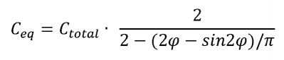
여기서, Ctotal은 총 커패시턴스 값이고, φ는 (i) 90°와 180° 사이 또는 (ii) 0°와 180° 사이의 위상각이며, 상기 스위치의 온-타임은 위상각을 기반으로 한다. 상기 동조 가능한 리액턴스 회로는 제1 용량성 리액턴스와 제2 용량성 리액턴스 사이에 연속적으로 또는 이산적으로 동조 가능한 용량성 리액턴스를 제시하도록 구성될 수 있다. 상기 스위치는 MOSFET일 수 있고, 상기 다이오드는 MOSFET의 바디 다이오드(body diode)이다. 예시적인 시스템은 동작 주파수에서 구동 신호를 출력하도록 구성된 구동 회로, 및 상기 구동 신호에 기초하여 전자기장을 생성하도록 구성된 공진기를 포함할 수 있다. 상기 동조 가능한 리액턴스 회로는 교류에 의해 전력이 공급될 때 동조 가능한 용량성 리액턴스를 제시하도록 구성된다.where C total is the total capacitance value, φ is the phase angle (i) between 90° and 180° or (ii) between 0° and 180°, and the on-time of the switch is based on the phase angle. The tunable reactance circuit may be configured to present a tunable capacitive reactance either continuously or discretely between the first capacitive reactance and the second capacitive reactance. The switch may be a MOSFET, and the diode is a body diode of the MOSFET. An example system can include a drive circuit configured to output a drive signal at an operating frequency, and a resonator configured to generate an electromagnetic field based on the drive signal. The tunable reactance circuit is configured to present a tunable capacitive reactance when powered by alternating current.
상기 게이트 드라이버는 부트스트랩 파워 서플라이에 결합될 수 있으며, 여기서 부트스트랩 파워 서플라이는 상기 구동 회로의 적어도 일부의 전도 (예를 들어, 로우 사이드(low-side) 스위치 전도 시간) 동안 충전하도록 구성된 부트스트랩 커패시터를 포함할 수 있다. 상기 구동 회로는 인버터일 수 있다. 상기 송신기는 상기 인버터의 하나 이상의 게이트 드라이버 및 상기 동조 가능한 리액턴스 회로의 게이트 드라이버에 전력을 공급하도록 구성된 보조 전원을 더 포함할 수 있다. 상기 보조 전원은 절연 DC-DC 컨버터일 수 있다. 상기 동조 가능한 리액턴스 회로는 송신기에서 반사된 임피던스를 기반으로 용량성 리액턴스를 제시하도록 구성될 수 있다. 상기 동조 가능한 리액턴스 회로는 상기 송신기의 전력 특성을 기반으로 용량성 리액턴스를 제시하도록 구성될 수 있다. 상기 송신기는 상기 동조 가능한 리액턴스 회로와 상기 공진기 사이에 결합된 인덕터를 더 포함할 수 있다.The gate driver may be coupled to a bootstrap power supply, wherein the bootstrap power supply is configured to charge during conduction (e.g., low-side switch conduction time) of at least a portion of the drive circuitry. Capacitors may be included. The driving circuit may be an inverter. The transmitter may further include an auxiliary power supply configured to supply power to one or more gate drivers of the inverter and gate drivers of the tunable reactance circuit. The auxiliary power source may be an isolated DC-DC converter. The tunable reactance circuit may be configured to present a capacitive reactance based on the impedance reflected from the transmitter. The tunable reactance circuit may be configured to present a capacitive reactance based on the power characteristics of the transmitter. The transmitter may further include an inductor coupled between the tunable reactance circuit and the resonator.
상기 동조 가능한 리액턴스 회로는 제1 용량성 리액턴스와 제2 용량성 리액턴스 사이에서 연속적으로 동조 가능한 용량성 리액턴스를 제시하도록 구성될 수 있다. 상기 동조 가능한 리액턴스 회로는 제1 용량성 리액턴스와 제2 용량성 리액턴스 사이에 이산적으로 동조 가능한 용량성 리액턴스를 제시하도록 구성될 수 있다. 상기 스위치는 금속 산화물 반도체 전계 효과 트랜지스터(MOSFET)일 수 있다. 상기 송신기의 출력 전력은 상기 동조 가능한 리액턴스 회로의 출력 리액턴스를 기반으로 할 수 있다. 상기 적어도 하나의 동조 가능한 리액턴스 회로는 제1 동조 가능한 리액턴스 회로 및 제2 동조 가능한 리액턴스 회로를 포함하고, 상기 구동 회로는 상기 제2 동조 가능한 리액턴스 회로의 입력에 결합된 제2 출력 노드를 갖고, 상기 공진기는 상기 제2 동조 가능한 리액턴스 회로의 출력에 결합된 제2 입력 노드를 갖는다. 상기 제1 동조 가능한 리액턴스 회로의 커패시턴스 값은 상기 제2 동조 가능한 리액턴스 회로의 커패시턴스 값과 동일하다.The tunable reactance circuit may be configured to present a tunable capacitive reactance continuously between the first capacitive reactance and the second capacitive reactance. The tunable reactance circuit may be configured to present a discrete tunable capacitive reactance between the first capacitive reactance and the second capacitive reactance. The switch may be a metal oxide semiconductor field effect transistor (MOSFET). The output power of the transmitter may be based on the output reactance of the tunable reactance circuit. wherein the at least one tunable reactance circuit includes a first tunable reactance circuit and a second tunable reactance circuit, the drive circuit having a second output node coupled to an input of the second tunable reactance circuit; The resonator has a second input node coupled to the output of the second tunable reactance circuit. A capacitance value of the first tunable reactance circuit is equal to a capacitance value of the second tunable reactance circuit.
상기 시스템은 상기 동조 가능한 리액턴스 회로의 입력에 결합된 제1 출력 노드를 갖는 공진기; 및 상기 동조 가능한 리액턴스 회로의 출력에 결합된 정류기를 포함한다. 상기 동조 가능한 리액턴스 회로는 교류에 의해 전력이 공급될 때 동조 가능한 용량성 리액턴스를 제시하도록 구성된다. 상기 게이트 드라이버는 부트스트랩 파워 서플라이에 결합될 수 있으며, 여기서 상기 부트스트랩 파워 서플라이는 상기 정류기의 적어도 일부의 전도 동안(예를 들어, 로우 사이드 다이오드 전도 시간 동안) 충전하도록 구성된 부트스트랩 커패시터를 포함할 수 있다. 상기 수신기는 상기 동조 가능한 리액턴스 회로의 게이트 드라이버에 전력을 공급하도록 구성된 보조 전원을 포함할 수 있다. 상기 보조 전원은 절연 DC-DC 컨버터일 수 있다. 상기 동조 가능한 리액턴스 회로는 상기 수신기의 반사 임피던스를 수정하기 위한 용량성 리액턴스를 제시하도록 구성될 수 있다. 상기 동조 가능한 리액턴스 회로는 상기 수신기의 전력 특성을 기반으로 용량성 리액턴스를 제시하도록 구성될 수 있다. 상기 수신기는 상기 동조 가능한 리액턴스 회로와 상기 공진기 사이에 결합된 인덕터를 포함할 수 있다.The system includes a resonator having a first output node coupled to the input of the tunable reactance circuit; and a rectifier coupled to the output of the tunable reactance circuit. The tunable reactance circuit is configured to present a tunable capacitive reactance when powered by alternating current. The gate driver may be coupled to a bootstrap power supply, wherein the bootstrap power supply may include a bootstrap capacitor configured to charge during conduction of at least a portion of the rectifier (eg, during low side diode conduction time). can The receiver may include an auxiliary power supply configured to supply power to a gate driver of the tunable reactance circuit. The auxiliary power source may be an isolated DC-DC converter. The tunable reactance circuit may be configured to present a capacitive reactance to modify the reflected impedance of the receiver. The tunable reactance circuit may be configured to present a capacitive reactance based on the power characteristics of the receiver. The receiver may include an inductor coupled between the tunable reactance circuit and the resonator.
상기 동조 가능한 리액턴스 회로는 제1 용량성 리액턴스와 제2 용량성 리액턴스 사이에서 연속적으로 동조 가능한 용량성 리액턴스를 제시하도록 구성될 수 있다. 상기 동조 가능한 리액턴스 회로는 제1 용량성 리액턴스와 제2 용량성 리액턴스 사이에 이산적으로 동조 가능한 용량성 리액턴스를 제시하도록 구성될 수 있다. 상기 스위치는 금속 산화물 반도체 전계 효과 트랜지스터(MOSFET)일 수 있다. 부하에 전달되는 전력은 상기 동조 가능한 리액턴스 회로의 출력 리액턴스를 기반으로 할 수 있다. 상기 적어도 하나의 동조 가능한 리액턴스 회로는 제1 동조 가능한 리액턴스 회로 및 제2 동조 가능한 리액턴스 회로를 포함할 수 있고, 상기 공진기는 상기 제2 동조 가능한 리액턴스 회로의 입력에 결합된 제2 출력 노드를 갖고 상기 정류기는 상기 제2 동조 가능한 리액턴스 회로의 출력에 결합된 제2 입력 노드를 갖는다. 상기 제1 동조 가능한 리액턴스 회로의 커패시턴스 값은 상기 제2 동조 가능한 리액턴스 회로의 커패시턴스 값과 동일하다.The tunable reactance circuit may be configured to present a tunable capacitive reactance continuously between the first capacitive reactance and the second capacitive reactance. The tunable reactance circuit may be configured to present a discrete tunable capacitive reactance between the first capacitive reactance and the second capacitive reactance. The switch may be a metal oxide semiconductor field effect transistor (MOSFET). The power delivered to the load may be based on the output reactance of the tunable reactance circuit. The at least one tunable reactance circuit may include a first tunable reactance circuit and a second tunable reactance circuit, wherein the resonator has a second output node coupled to an input of the second tunable reactance circuit and wherein the resonator has a second output node coupled to an input of the second tunable reactance circuit. The rectifier has a second input node coupled to the output of the second tunable reactance circuit. A capacitance value of the first tunable reactance circuit is equal to a capacitance value of the second tunable reactance circuit.
도 1은 본 명세서에 설명된 하나 이상의 예시적인 동조 가능한 리액턴스 회로를 포함하는 예시적인 무선 전력 시스템의 블록도이다.
도 2는 다이오드에 병렬로 결합된 하나 이상의 커패시터를 포함하는 예시적인 단일 스위치 동조 가능한 리액턴스 회로의 개략도이다.
도 3a는 동조 가능한 리액턴스 회로를 제어하도록 구성된 PWM 제어 신호를 나타내는 전압 신호의 플롯이다. 도 3b는 예시적인 무선 전력 송신기의 동조 가능한 리액턴스 회로로의 인버터로부터의 전류를 나타내는 전류 신호의 플롯이다. 도 3c는 (i) 도 2의 회로의 스위치에서 전류를 나타내는 전류 신호; (ii) 도 2의 회로의 커패시터(들)에서의 전류를 나타내는 전류 신호; 및 (iii) 도 2의 회로의 다이오드의 전류를 나타내는 전류 신호의 플롯이다. 도 3d는 도 2의 회로의 노드들 사이의 전압 신호의 플롯이다.
도 4a-4b는 도 3a-3d에 도시된 위상 지연 phi(각도 단위)의 함수로서 단일 스위치 동조 가능한 리액턴스 회로의 리액턴스의 리액턴스 플롯이다.
도 5a-5b는 부트스트랩 기반 파워 서플라이의 커패시터를 충전하는 동안 송신기를 도시하는, 하나 이상의 예시적인 단일 스위치 동조 가능한 리액턴스 회로를 포함하는 예시적인 무선 전력 송신기의 일부에 대한 개략도이다.
도 6a는 (i) 램프업(ramp-up) 동안 제1 하부 스위치의 게이트와 접지 사이의 전압차를 나타내는 전압 신호; 및 (ii) 램프업 동안 제2 하부 스위치의 게이트와 접지 사이의 전압차를 나타내는 전압 신호의 플롯이다. 도 6b는 (i) 램프업 동안 제1 부트스트랩 커패시터 양단의 전압 신호 및 (ii) 램프업 동안 제2 부트스트랩 커패시터 양단의 전압 신호의 플롯이다. 도 6c는 (i) 램프업 동안 제1 부트스트랩 다이오드를 통한 전류 신호 및 (ii) 램프업 동안 제2 부트스트랩 다이오드를 통한 전류 신호의 플롯이다.
도 7a는 (i) 정상 상태 동안 제1 하부 스위치의 게이트와 접지 사이의 전압 차이를 나타내는 전압 신호; 및 (ii) 정상 상태 동안 제2 하부 스위치의 게이트와 접지 사이의 전압 차를 나타내는 전압 신호의 플롯이다. 도 7b는 (i) 정상 상태 동안 제1 부트스트랩 커패시터 양단의 전압 신호 및 (ii) 정상 상태 동안 제2 부트스트랩 커패시터 양단의 전압 신호의 플롯이다. 도 7c는 (i) 정상 상태 동안 제1 부트스트랩 다이오드를 통한 전류 신호 및 (ii) 정상 상태 동안 제2 부트스트랩 다이오드를 통한 전류 신호의 플롯이다.
도 8은 하나 이상의 예시적인 단일 스위치 동조 가능한 리액턴스 회로를 포함하는 예시적인 무선 전력 수신기의 일부의 개략도이다.
도 9는 동조 가능한 리액턴스 회로의 실시예의 개략도이다.
도 10a-10b는 동조 가능한 리액턴스 회로가 있거나 없는 무선 전력 송신기에 대한 동조 가능한 리액턴스 범위를 도시하는 표이다.
도 11은 도 9의 동조 가능한 리액턴스 회로를 포함하는 송신기의 일부의 개략도이다.
도 12는 도 9의 동조 가능한 리액턴스 회로를 포함하는 수신기의 일부의 개략도이다.
도 13은 도 9의 동조 가능한 리액턴스 회로를 포함하는 수신기의 일부의 개략도이다.
도 14a-14d는 도 13의 수신기 부분에서 신호의 플롯이다.
도 15a-15d는 도 13의 수신기 부분에서 신호의 플롯이다.
도 16a-16b는 도 13의 수신기 부분에서 위상각의 함수로서 신호의 플롯이다.
도 17은 본 명세서에 설명된 시스템 및 방법을 구현하는데 사용될 수 있는 예시적인 컴퓨터 시스템의 블록도이다.1 is a block diagram of an example wireless power system that includes one or more example tunable reactance circuits described herein.
2 is a schematic diagram of an exemplary single switch tunable reactance circuit including one or more capacitors coupled in parallel to a diode.
3A is a plot of a voltage signal representing a PWM control signal configured to control a tunable reactance circuit. 3B is a plot of a current signal representing current from an inverter into a tunable reactance circuit of an exemplary wireless power transmitter. Figure 3c shows (i) a current signal representing the current in the switch of the circuit of Figure 2; (ii) a current signal representative of the current in the capacitor(s) of the circuit of FIG. 2; and (iii) a plot of the current signal representing the current of the diode of the circuit of FIG. 2. 3D is a plot of voltage signals between nodes of the circuit of FIG. 2;
Figures 4a-4b are reactance plots of the reactance of the single switch tunable reactance circuit as a function of the phase delay phi (in degrees) shown in Figures 3a-3d.
5A-5B are schematic diagrams of a portion of an exemplary wireless power transmitter including one or more exemplary single switch tunable reactance circuits showing the transmitter while charging a capacitor of a bootstrap based power supply.
6A shows (i) a voltage signal representing a voltage difference between the gate of the first lower switch and ground during ramp-up; and (ii) a voltage signal representing the voltage difference between the gate of the second lower switch and ground during ramp-up. 6B is a plot of (i) the voltage signal across the first bootstrap capacitor during ramp-up and (ii) the voltage signal across the second bootstrap capacitor during ramp-up. 6C is a plot of (i) the current signal through the first bootstrap diode during ramp-up and (ii) the current signal through the second bootstrap diode during ramp-up.
7A shows (i) a voltage signal representing a voltage difference between the gate of the first lower switch and ground during a steady state; and (ii) a voltage signal representing the voltage difference between the gate of the second lower switch and ground during steady state. 7B is a plot of (i) the voltage signal across the first bootstrap capacitor during steady state and (ii) the voltage signal across the second bootstrap capacitor during steady state. 7C is a plot of (i) the current signal through the first bootstrap diode during steady state and (ii) the current signal through the second bootstrap diode during steady state.
8 is a schematic diagram of a portion of an example wireless power receiver that includes one or more example single switch tunable reactance circuits.
9 is a schematic diagram of an embodiment of a tunable reactance circuit.
10A-10B are tables showing tunable reactance ranges for a wireless power transmitter with and without a tunable reactance circuit.
11 is a schematic diagram of a portion of a transmitter that includes the tunable reactance circuit of FIG. 9;
12 is a schematic diagram of a portion of a receiver that includes the tunable reactance circuit of FIG. 9;
13 is a schematic diagram of a portion of a receiver that includes the tunable reactance circuit of FIG. 9;
14a-14d are plots of signals in the receiver portion of FIG. 13;
15a-15d are plots of signals in the receiver portion of FIG. 13;
16a-16b are plots of the signal as a function of phase angle in the receiver portion of FIG. 13;
17 is a block diagram of an exemplary computer system that can be used to implement the systems and methods described herein.
동조 가능한 임피던스, 보다 구체적으로 동조 가능한 리액턴스를 제공하기 위한 전자 회로, 시스템 및 방법이 본 명세서에 개시된다. 동조 가능한 리액턴스 회로의 실시예는 특정 레벨의 전력을 및/또는 특정 효율로 부하, 예를 들어 배터리에 전달하기 위한 무선 전력 송신기 및/또는 수신기를 포함하는 무선 전력 시스템에서 활용될 수 있다.Disclosed herein are electronic circuits, systems and methods for providing tunable impedance, and more specifically tunable reactance. Embodiments of tunable reactance circuits may be utilized in wireless power systems that include wireless power transmitters and/or receivers for delivering specific levels of power and/or specific efficiencies to a load, such as a battery.
무선 전력 시스템wireless power system
도 1은 하나 이상의 예시적인 동조 가능한 리액턴스 회로를 포함하는 예시적인 무선 전력 시스템(100)의 블록도이다. 시스템(100)은 무선 전력 송신기(102) 및 무선 전력 수신기(104)를 포함한다. 송신기(102)에서, 파워 서플라이(105)(예를 들어, AC 주전원, 배터리 등)는 인버터(108)에 전력을 제공한다. 추가 컴포넌트는 인버터 스테이지(108) 이전에 역률 보정(PFC) 회로(106)를 포함할 수 있다. 인버터(108)는 임피던스 정합 네트워크(110)(고정 및/또는 동조 가능한 네트워크 컴포넌트 포함)를 통해 송신기 공진기 코일 및 용량성 컴포넌트(112)("공진기")를 구동한다. 송신기 공진기는 수신기 공진기에서 전류 및/또는 전압을 유도하는 발진 자기장을 생성한다. 수신된 에너지는 임피던스 정합 네트워크(116)(고정 및/또는 동조 가능한 네트워크 컴포넌트 포함)를 통해 정류기(118)에 제공된다. 궁극적으로, 정류된 전력은 부하(120)(예를 들어, 전기 또는 하이브리드 차량의 하나 이상의 배터리)에 제공된다. 일부 실시예들에서, 배터리 전압 레벨은 무선 전력 시스템(100)의 다양한 파라미터들(예를 들어, 임피던스)에 영향을 미칠 수 있다. 따라서, 배터리 전압 레벨은 무선 전력 시스템(100)의 다른 부분들에 대한 입력으로서 제공되도록 수신, 결정 또는 측정될 수 있다. 예를 들어, 전기 자동차의 전형적인 배터리 전압 범위는 280-420V이다.1 is a block diagram of an example
일부 실시예에서, 송신기(102)의 하나 이상의 컴포넌트는 수신기(104)의 통신 모듈(예를 들어, Wi-Fi, 라디오, 블루투스, 대역내(in-band) 시그널링 메커니즘 등)과 통신하도록 구성된 통신 모듈을 포함할 수 있는 제어기(122)에 결합될 수 있다. 일부 실시예에서, 송신기(102)의 하나 이상의 컴포넌트는 하나 이상의 센서(124)(예를 들어, 전류 센서, 전압 센서, 전력 센서, 온도 센서, 고장 센서 등)에 결합될 수 있다. 제어기(122) 및 센서(들)(124)는 센서(들)(124) 및/또는 센서(들)(128)로부터의 피드백 신호에 기초하여 송신기(102)의 제어 부분에 작동 가능하게 결합될 수 있다.In some embodiments, one or more components of
일부 실시예에서, 수신기(104)의 하나 이상의 컴포넌트는 송신기(102)의 통신 모듈(예를 들어, Wi-Fi, 라디오, 블루투스, 대역내 시그널링 메커니즘 등)과 통신하도록 구성된 통신 모듈을 포함할 수 있는 제어기(126)에 결합될 수 있다. 일부 실시예에서, 송신기(104)의 하나 이상의 컴포넌트는 하나 이상의 센서(128)(예를 들어, 전류 센서, 전압 센서, 전력 센서, 온도 센서, 고장 센서 등)에 결합될 수 있다. 제어기(126) 및 센서(들)(128)는 센서(들)(128) 및/또는 센서(들)(124)로부터의 피드백 신호에 기초하여 송신기(102)의 제어 부분에 작동 가능하게 결합될 수 있다.In some embodiments, one or more components of
무선 전력 시스템의 예는 "무선 에너지 전달 시스템"이라는 제목으로 2010년 6월 10일에 공개된 미국 특허 출원 공개 번호 2010/0141042 및 "차량용 무선 에너지 전송"이라는 제목으로 2012년 5월 10일에 공개된 미국 특허 출원 공개 번호 2012/0112535에서 찾을 수 있고, 이들 둘 모두는 전체 내용이 참고로 본 명세서에 통합된다.Examples of wireless power systems are US Patent Application Publication No. 2010/0141042, published on June 10, 2010, entitled "Wireless Energy Transfer Systems," and published May 10, 2012, entitled "Wireless Energy Transmission for Vehicles." Published US Patent Application No. 2012/0112535, both of which are incorporated herein by reference in their entirety.
고전력 무선 전력 송신기는 고전력에 의존하는 차량, 산업 기계, 로봇 또는 전자 디바이스의 전력 공급 및/또는 배터리 충전과 같은 애플리케이션에서 무선 전력을 송신하도록 구성될 수 있다. 예시의 목적으로, 이하의 개시는 차량용 무선 전력 송신에 초점을 맞춘다. 그러나, 본 명세서에 설명된 실시예 중 임의의 하나 이상이 무선 전력이 활용될 수 있는 다른 애플리케이션에 적용될 수 있다는 것이 이해된다.A high power wireless power transmitter may be configured to transmit wireless power in applications such as powering and/or battery charging of vehicles, industrial machinery, robots or electronic devices that rely on high power. For purposes of illustration, the following disclosure focuses on vehicular wireless power transmission. However, it is understood that any one or more of the embodiments described herein may be applied to other applications in which wireless power may be utilized.
동조 가능한 임피던스 정합 네트워크Tunable Impedance Matching Network
일부 실시예에서, 예시적인 임피던스 정합 네트워크(IMN)(110, 116)는 하나 이상의 가변 임피던스 성분을 포함할 수 있다. 하나 이상의 가변 임피던스 성분은 본 명세서에서 함께 "동조 가능한 정합 네트워크(TMN)"로 지칭될 수 있다. 임피던스는 다음과 같이 데카르트 형식(Cartesian form)으로 표현될 수 있다:In some embodiments, exemplary impedance matching networks (IMNs) 110, 116 may include one or more variable impedance components. One or more variable impedance components may together be referred to herein as a “tunable matching network (TMN)”. Impedance can be expressed in Cartesian form as:
![]()
![]()
여기서, 임피던스의 실수부는 저항 R이고, 허수부는 리액턴스 X이다. TMN은 무선 전력 송신기(102) 및/또는 수신기(104)의 임피던스(예를 들어, 리액턴스 X를 포함)를 조정하는 데 사용될 수 있다.Here, the real part of the impedance is the resistance R, and the imaginary part is the reactance X. TMN may be used to adjust the impedance (eg, including reactance X) of the
일부 실시예에서, 동조 가능한 정합 네트워크(들)는 "동조 가능한 리액턴스 회로(들)"로 지칭될 수 있다. 일부 애플리케이션, 예를 들어, 무선 전력 송신에서, 무선 전력 송신기(102)에 의해 보여지고/보이거나 수신기(104)에 의해 제시되는 임피던스는 동적으로 변할 수 있다. 그러한 애플리케이션에서, 수신기 공진기 코일(114)과 부하(120) 사이, 그리고 송신기 공진기 코일(112)과 파워 서플라이(105) 사이의 임피던스 정합은 불필요한 에너지 손실과 과도한 열을 방지하는 데 유리할 수 있다. 공진기 코일에 의해 또는 공진기 코일 상에서 반사되는 임피던스는 동적일 수 있으며, 이 경우 동적 임피던스 정합 네트워크는 시스템 (100)의 성능(예를 들어, 효율성, 전력 전달 등)을 개선하기 위해 가변 임피던스를 보상하도록 조정될 수 있다. 무선 전력 시스템(100)의 인버터(108)의 경우, 인버터(108)에 의해 보여지는 임피던스는 전력을 수신하는 부하(120)(예를 들어, 배터리 또는 배터리 충전 회로부(circuitry))의 변화와 송신기(102)와 수신기(104) 사이의 결합의 변화로(예를 들어, 송신기 및 수신기 공진기 코일의 상대 위치의 변화에 의해 유발됨) 인해 매우 가변적일 수 있다. 유사하게, 수신기 공진기(114)에 부하를 가하는 임피던스는 전력을 수신하는 부하(120)의 변화로 인해 동적으로 변화될 수 있다. 또한, 수신기 공진기(114)에 대한 원하는 임피던스 정합은 다른 결합 조건 및/또는 전력 공급 조건에 따라 상이할 수 있다.In some embodiments, the tunable matching network(s) may be referred to as “tunable reactance circuit(s)”. In some applications, eg, wireless power transmission, the impedance seen by
따라서, 예를 들어 고 공진 무선 전력 전송을 통해 전력을 송신 및/또는 수신하는 전력 전송 시스템은 효율적인 전력 송신을 유지하고 및/또는 특정 레벨의 전력을 부하(120)에 전달하기 위해 동조 가능하거나 가변적인 임피던스 정합 네트워크(110, 116)를 활용할 수 있다. 예를 들어, TMN의 하나 이상의 컴포넌트는 TMN의 특정 컴포넌트에 의해 달성 가능한 최소 임피던스와 최대 임피던스 사이의 임피던스를 제시하도록 구성될 수 있다. 다양한 실시예에서, 달성 가능한 임피던스는 무선 전력 시스템(100)의 동작 주파수(예를 들어, 80kHz 내지 90kHz)에 의존할 수 있다. 동조(tuning)는 연속적으로, 간헐적으로, 또는 전력 송신의 특정 지점(예를 들어, 전력 송신 시작에서 또는 전력 송신 동안). 동조 가능한 정합 네트워크의 예는 "무선 전력 전송 시스템 제어"라는 제목으로 2017년 8월 3일에 공개된 미국 특허 출원 공개 번호 2017/0217325와 "PWM 커패시터 제어"라는 제목으로 2017년 8월 10일에 공개된 미국 특허 출원 공개 번호 2017/0229917에서 찾아볼 수 있고, 둘 모두의 전체 내용이 참고로 본 출원에 통합된다.Thus, a power transfer system that transmits and/or receives power, for example via high resonant wireless power transfer, may be tunable or variable to maintain efficient power transmission and/or deliver a specific level of power to load 120. In
본 명세서에 사용되는, 용어 "커패시터" 또는 그에 대한 기호는 커패시턴스(예를 들어, 패럿(Farad) 단위) 및/또는 커패시턴스 리액턴스(예를 들어, 옴(Ohm) 단위)를 갖는 하나 이상의 전기 컴포넌트를 지칭할 수 있다. 예를 들어, 커패시터는 수십, 수백 등의 이산 커패시터 정도일 수 있는 하나 이상의 커패시터(예를 들어, 커패시터의 "뱅크(bank)"에)를 포함할 수 있다. 원하는 커패시턴스 및/또는 원하는 커패시턴스 리액턴스를 얻기 위해 2개 이상의 커패시터가 직렬 또는 병렬로 결합될 수 있다. 용량성 리액턴스는 본 명세서에서 음의 값으로 표현될 수 있음을 유의한다. 그러나, 당업자는 일부 관례에서 용량성 리액턴스가 또한 양의 값으로 표현될 수 있음을 인식할 것이다. 도면을 포함하는 개시가 다양한 전기 컴포넌트에 대한 예시적인 값을 제공할 수 있지만, 컴포넌트들의 값은 특정 애플리케이션에 대해 맞춤화될 수 있는 것으로 이해된다. 예를 들어, 무선 전력 송신기가 차량 배터리(수천 와트 정도) 또는 휴대폰 배터리(전형적으로 5와트 미만)를 충전하기 위한 전력을 송신하는 데 사용되는지 여부에 따라 다양한 전자 컴포넌트의 값이 달라질 수 있다.As used herein, the term “capacitor” or symbols for it refer to one or more electrical components having capacitance (eg, in Farads) and/or capacitance reactance (eg, in Ohms). can be referred to For example, the capacitors may include one or more capacitors (eg, in a “bank” of capacitors) which may be on the order of tens, hundreds, etc. of discrete capacitors. Two or more capacitors may be coupled in series or parallel to obtain a desired capacitance and/or desired capacitance reactance. Note that capacitive reactance can be expressed as a negative value herein. However, one skilled in the art will recognize that in some conventions capacitive reactance can also be expressed as a positive value. Although the disclosure, including the drawings, may provide example values for various electrical components, it is understood that the values of components may be tailored for a particular application. For example, depending on whether the wireless power transmitter is being used to transmit power to charge a vehicle battery (on the order of thousands of watts) or a cell phone battery (typically less than 5 watts), various electronic components may have different values.
단일 스위치 동조 가능한 리액턴스 회로Single switch tunable reactance circuit
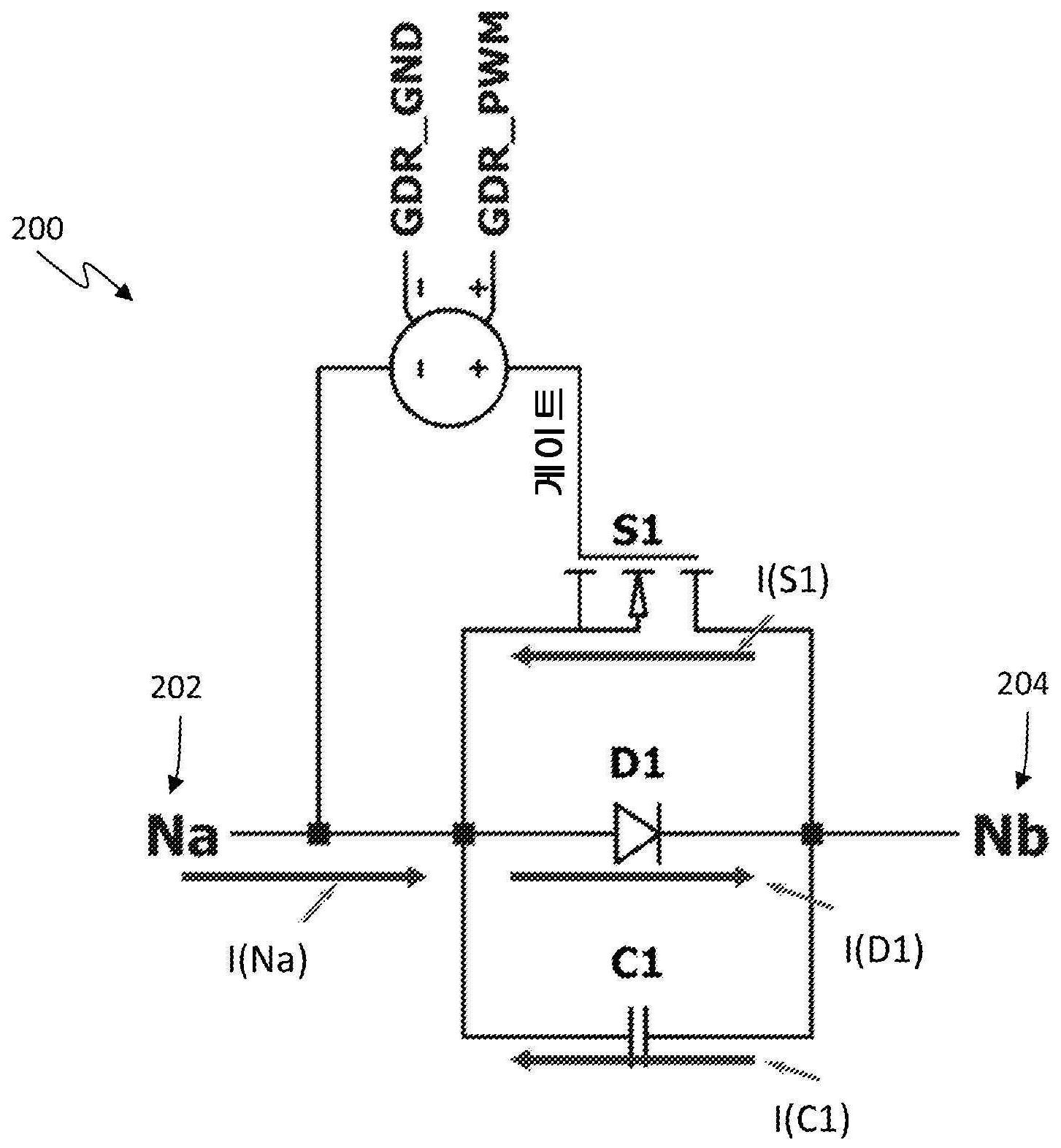
도 2는 다이오드 D1에 병렬로 결합된 하나 이상의 커패시터 C1을 포함하는 단일 스위치 동조 가능한 리액턴스 회로(200)를 도시한다. 다이오드 D1는 스위치 S1에 역병렬로 결합된다. 스위치 S1은 트랜지스터(예를 들어, 전계 효과 트랜지스터(FET), 금속 산화물 반도체 FET(MOSFET), 절연 게이트 바이폴라 트랜지스터(IGBT), 바이폴라 접합 트랜지스터(BJT) 등)일 수 있다. 스위치(S1)가 양의 전류만을 전달하도록 구성되는 경우, 다이오드 D1는 도 3a-3d에 대해 추가로 후술되는 바와 같이, 음의 전류 동안 전류가 흐르는 경로를 제공하도록 결합된다. 일부 실시예에서, 스위치는 음의 전류를 전도할 수 있는 MOSFET일 수 있다. MOSFET의 경우, 다이오드 D1은 MOSFET의 바디 다이오드이다.2 shows a single switch
스위치 S1은 펄스 폭 변조(PWM) 제어 신호("GDR_PWM")에 의해 제어될 수 있다. PWM 제어 신호는 동작 주파수 기간의 50%의 듀티 사이클을 가질 수 있으며, 여기서 스위칭 기간은 무선 전력 시스템(100)의 동작 주파수(예를 들어, 80 내지 90kHz 사이)의 역수로 정의된다. 스위치 S1에 대한 스위치 게이팅 기능은 노드 "Na"(202)로의 전류의 제로 크로싱(zero crossing)과 동기화될 수 있다.Switch S1 may be controlled by a pulse width modulation (PWM) control signal (“GDR_PWM”). The PWM control signal may have a duty cycle of 50% of the operating frequency period, where the switching period is defined as the reciprocal of the operating frequency of the wireless power system 100 (eg, between 80 and 90 kHz). The switch gating function for switch S1 can be synchronized with the zero crossing of the current into node “Na” (202).
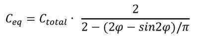
일부 실시예에서, 스위치 S1 온-타임(on-time)은 무선 전력 송신기(102) 또는 수신기(104)의 동작에서 주어진 시간에 원하는 등가 커패시턴스에 기초할 수 있다. 등가 커패시턴스 Ceq는 다음과 같이 결정될 수 있다:In some embodiments, switch S1 on-time may be based on a desired equivalent capacitance at a given time in operation of

여기서, C1은 상기에서 논의된 하나 이상의 커패시터의 값이고, φ는 노드 Na로부터 동조 가능한 리액턴스 회로로의 전류 I(Na)의 제로 크로싱과 스위치 S1의 턴-오프 사이의 위상 지연이다. 따라서 스위치 S1 온-타임은 위상 지연 φ를 기반으로 한다.where C1 is the value of one or more of the capacitors discussed above, and φ is the phase delay between the zero crossing of the current I(Na) from node Na into the tunable reactance circuit and the turn-off of switch S1. Therefore, the switch S1 on-time is based on the phase delay φ.
도 3a는 PWM 제어 신호를 나타내는 전압 신호 V(GDR_PWM)의 플롯이다. 도 3b는 인버터(108)로부터 송신기(102)의 동조 가능한 리액턴스 회로(200)로의 전류를 나타내는 전류 신호 I(Na)의 플롯이다. 도 3c는 (i) 스위치 S1에서의 전류를 나타내는 전류 신호 I(S1); (ii) 커패시터(들) C1에서의 전류(예를 들어, 커패시터(들)(C1)의 측 상의 노드에서 측정된 전류, 계산된 전류(전류 I = C*dV/dt) 등)를 나타내는 전류 신호 I(C1); 및 (iii) 다이오드 D1의 전류를 나타내는 전류 신호(I(D1))의 플롯이다. 도 3d는 노드 Na(202)와 노드 Nb(204) 사이의 전압 신호 V(Na,Nb)의 플롯이다. 도시된 바와 같이, 위상 지연 φ는 전류 I(Na)의 제로 크로싱과 전압 신호 V(GDR_PWM)의 턴-오프 사이의 차이이다. 노드 Na로부터 동조 가능한 리액턴스 회로(200)로의 거의 사인파 I(Na) 전류를 가정하면, 스위치 S1의 턴-온과 노드 Na에 대한 동조 가능한 리액턴스 회로(200)로의 전류 I(Na)의 제로 크로싱 사이의 위상 지연 0˚에서 φ까지 어디에서나 될 수 있다. 제로 크로싱 위상 지연에 대한 턴-온이 φ와 같으면, 게이트 구동 신호의 온-타임이 제로 크로싱과 중앙 정렬된다. 실제로 그리고 도 3a 내지 도 3d에 도시된 바와 같이, 턴-온 지연(302)이 추가되어 스위치가 턴 온 되기 전에 스위치 S1 양단의 전압(V(Na, Nb))이 제로에 도달하는 것을 보장하고 다이오드 전도 시간을 최소화하기 위해, 제로 교차 위상 지연에 대한 턴-온(turn-on)이 φ보다 약간 작도록 한다. 표기법 ![]()
![]()
도 4a는 전술한 바와 같이 위상 지연 φ(각도)의 함수로서 단일 스위치 동조 가능한 리액턴스 회로(200)의 리액턴스의 플롯이다. 특히, 커패시터(들)의 예시적인 커패시턴스 C1 = 187nF 및 90°와 180°의 φ에 대해, 회로(200)는 85kHz에서 대략 -5 내지 0 옴의 용량성 리액턴스를 생성할 수 있다. 도 4b를 참조하면, 커패시터(들)의 예시적인 커패시턴스 C1 = 187 nF 및 0°와 180° 사이의 φ에 대해, 회로(200)는 85kHz에서 대략 -10 내지 0 옴의 용량성 리액턴스를 생성할 수 있다. 이 예에서, 송신기(102)에 대해 187nF의 커패시턴스는 각각의 뱅크가 38개의 병렬 커패시터들을 갖는 직렬로 2개의 커패시터 뱅크들을 포함함으로써 10nF의 베이스 커패시턴스 값으로 획득될 수 있다.Figure 4a is a plot of the reactance of the single switch
일부 실시예에서, 단일 스위치 동조 가능한 리액턴스 회로(200)의 스위치 S1의 게이트 드라이버는 게이트 드라이버에 대해 절연된 DC-DC 컨버터들을 요구하는 대신에, 추가로 후술되는 바와 같이, 접지에 참조된 서플라이에 의해 충전되는 부트스트랩 회로(bootstrap circuit)에 의해 전력 공급될 수 있다.In some embodiments, the gate driver of switch S1 of single switch
무선 전력 시스템을 위한 단일 스위치 동조 가능한 리액턴스 회로Single switch tunable reactance circuit for wireless power systems
도 5a-5b는 예시적인 단일 스위치 동조 가능한 리액턴스 회로(502a, 502b)를 포함하는 예시적인 무선 전력 송신기의 부분(500a, 500b)(집합적으로 500으로 지칭됨)의 개략도이다. 예시적인 송신기 부분(500)에서, 단일 스위치 동조 가능한 리액턴스 회로(502a, 502ba)는 각각 상단 지로(upper branch)와 하단 지로(lower branch) 상에 채용된다. 상단 지로에서, 동조 가능한 리액턴스 회로(502a)는 인버터(108)(도 5a 참조)의 제1 출력 노드 NAA와 송신기 IMN(503)의 제1 입력 노드(NBA) 사이에 결합된다. 하단 지로에서, 동조 가능한 리액턴스 회로는 (502b_는 인버터(108)의 제2 출력 노드(NAB)와 송신기 IMN(503)의 제2 입력 노드(NBB) 사이에 결합된다. IMN(503)은 동조 가능한 리액턴스 회로(502a, 502b)와 송신기 공진기(501) 사이에 결합된다. 동조 가능한 리액턴스 회로(502a, 502b)가 부트스트랩 파워 서플라이(504a, 504b)에 의존하는 경우, 인버터(108)와 동조 가능한 리액턴스 회로(502a, 502b) 사이에는 어떠한 임피던스도 있을 수 없다는 것에 유의한다. 일부 실시예에서, 송신기 부분(500)은 동조 가능한 리액턴스 회로(502a 또는 502b)와 공진기(501) 사이에 결합된 인덕터를 더 포함할 수 있다.5A-5B are schematic diagrams of
2개의 개별 회로(502a, 502b)를 활용함으로써, 원하는 리액턴스가 2개의 지로에 걸쳐 "분할(split)" 되어서 송신기(102)에 균형 잡힌(balanced) 리액턴스가 제공된다. 90°와 180° 사이의 φ를 갖는 상기 예를 참조하면, C1= 187nF를 활용하는 개별 회로에 대해, 회로들(502a, 502b) 내의 대응하는 "분할된" 각각의 커패시터들(C1A, C1B)은 각각 대략 374nF와 동일할 수 있고, 따라서 총 직렬 등가 커패시턴스는 187nF이다. 상단 지로 회로(502a)는 하단 지로 회로(502b)와 직렬로 되어 있다는 것에 유의한다. 0°와 180° 사이의 φ가 있는 위의 예를 참조하면, C1= 187nF를 활용하는 개별 회로(200)에 대해, 회로(502a, 502b)의 대응하는 "분할된" 각각의 커패시터 (C1A, C1B)는 각각 대략 187nF와 동일할 수 있고, 따라서 총 직렬 등가 커패시턴스는 93.5nF이다.By utilizing two
부트스트랩 파워 서플라이(504a, 504b)는 각각 송신기(102)에서 회로(502a, 502b)를 구동할 수 있다. 부트스트랩 파워 서플라이(504a)는 노드 NAA와 부트스트랩 다이오드 DBOOT_A1의 출력 사이에 결합된 부트스트랩 커패시터 CBOOT_A1을 포함할 수 있다. 다이오드 DBOOT_A1은 DC 파워 서플라이 VDD에 의해 구동된다. 부트스트랩 파워 서플라이(504b)는 노드 NAB와 부트스트랩 다이오드 DBOOT_A1의 출력 사이에 결합된 부트스트랩 커패시터 CBOOT_B1를 포함할 수 있다. 다이오드 DBOOT_A1은 DC 파워 서플라이 VDD에 의해 구동된다. 서플라이 VDD는 하나 이상의 DC 파워 서플라이를 지칭할 수 있다는 것에 유의한다. 이 예에서, 부트스트랩 파워 서플라이(504a, 504b)는 (504a, 504b)에 의한 공급 및 스위치 S1A 및 S1B의 각 게이트를 구동하기 위한 단일 집적 회로(IC)(505)에 결합된다(예를 들어, 제어를 위한 PWM 신호 제공). 그러나, 다른 실시예에서, 서플라이(504a, 504b)는 각각 제어 목적을 위해 별도의 IC를 가질 수 있다. 다양한 실시예에서, 회로(502a)에 대한 제어 신호와 회로(502b)에 대한 제어 신호는 동기화된다. 이것은 여러 지로 이유로 유리하다. 동기화된 제어 신호는 섀시(chassis) 및/또는 접지에 대한 전위를 최소화하는 (송신기(500) 내의) 균형 잡힌 네트워크를 보장하기 위해 커패시턴스 값 C1A 및 C1B이 동일해질 수 있게 한다. 또한, 동기화된 제어 신호는 공진기(501)의 중심이 접지에 대해 제로 전위가 되도록 하며, 이는 전자기 간섭(EMI)을 특정 임계치 아래로 줄이거나 유지하는 데 중요할 수 있다. 일부 실시예에서, 회로(502a, 502b)는 상이한 커패시턴스 값 C1A 및 C1B을 초래하는 상이한 제어 신호로 구동될 수 있다. 회로(502a, 502b)가 2개의 개별 IC에 의해 제어되는 경우, IC가 동일한 제어 신호를 생성하도록 2개의 IC가 연결될 수 있다. 예를 들어, 동기화된 PWM 신호를 수신하기 위해 2개의 IC를 마스터 노드(예를 들어, 제어기, IC, 프로세서 등)에 결합하여 이를 수행할 수 있다.
다양한 실시예에서, 동조 가능한 리액턴스 회로(502a, 502b)는 송신기(102)의 동작 동안 하나 이상의 모드에서 동작할 수 있다. 예를 들어, 인버터(108)가 원하는 동작 상태(예를 들어, 전력, 특정 위상 편이(shift) 등)까지 램프업(ramp up)할 때, 회로(502a, 502b)는 단락되고 따라서 0 옴의 리액턴스를 갖는 무한 커패시턴스를 제공한다. 인버터(108)가 원하는 위상 편이(예를 들어, 최대 위상 편이 또는 180도)에 있으면, 회로(502a, 502b)는 0 옴에서 최소 용량성 리액턴스 -Xtx_minΩ(예를 들어, 90°의 φ에 대해 -5 옴(Ohms), 0°의 φ에 대해 -10 옴)과 및 최대 용량성 리액턴스 -Xtx_max Ω(예를 들어, 0 옴) 사이의 일부 값으로 조정할 수 있다.In various embodiments, the
도 6a 내지 도 6c는 송신기(102)의 램프업(또는 "스타트업(start-up)") 동안 송신기의 다양한 신호를 도시한다. 도 6a는 (i) 제1 하단 스위치 Slower1 의 게이트와 접지 PGND_GA사이의 전압차를 나타내는 전압 신호 V(Slower1-RGS2); 및 (ii) 제2 하단 스위치 Slower2의 게이트와 접지 PGND_GA 사이의 전압차를 나타내는 전압 신호 V(Slower2-RGS4)의 플롯이다. 전압 신호 V(Slower1-RGS2)의 지속 시간(602)은 Slower1 스위치의 온-타임을 나타내고, 전압 신호 V(Slower2-RGS4)의 지속 시간(604)은 Slower2 스위치의 온-타임을 나타낸다. 도 6b는 (i) 커패시터 CBOOT_A1 양단의 전압 신호 V(CBOOT_A1) 및 (ii) 커패시터 CBOOT_B1 양단의 전압 신호 V(CBOOT_B1)의 플롯이다. 전압 신호 V(CBOOT_A1)의 상승은 스위치 Slower2(지속 시간 604)의 온-타임 동안 발생하고, 전압 신호 V(CBOOT_A1)의 상승은 스위치 Slower1(지속 시간 602)의 온-타임 동안 발생한다. 도 6c는 (i) 부트스트랩 다이오드 DBOOT_A1을 통한 전류 신호 I(DBOOT_A1) 및 (ii) 부트스트랩 다이오드 DBOOT_A1을 통한 전류 신호 I(DBOOT_B1)의 플롯이다. 전류 신호 I(DBOOT_A1)의 하강은 스위치 Slower2의 온-타임(지속 시간 604) 동안 발생하고, 전류 신호 I(DBOOT_A1)의 하강은 스위치 Slower1의 온-타임(지속 시간 602) 동안 발생한다는 것에 유의한다.6A-6C show various signals of the
정상 상태에서, 회로(502a, 502b)는 특정 전력 레벨을 달성하거나 유지하기 위해 및/또는 원하는 범위 내에서 인버터 위상을 달성하거나 유지하기 위해 연속적으로, 간헐적으로 또는 주기적으로 조정될 수 있다. 예를 들어, 회로(들)(502a, 502b)의 리액턴스의 증가는 송신기(500)에 의한 증가된 출력 전력 및/또는 감소된 인버터 VI 위상 (예를 들어, 인버터(108)로부터의 전류 신호와 전압 신호 사이의 위상차)를 초래할 수 있다. 역으로, 회로(들)(502a, 502b)의 리액턴스의 감소는 송신기(500)에 의한 감소된 출력 전력 및/또는 증가된 인버터 위상을 초래할 수 있다. 회로(502a, 502b)는 사용된 전자 컴포넌트의 특성(예를 들어, C1 커패시턴스)에 기초하여 특정 최대 리액턴스 Xtx_max 및 최소 리액턴스 Xtx_min을 가질 수 있다.In steady state,
도 7a 내지 도 7c는 송신기(102)의 정상 상태 동작 동안 송신기의 다양한 신호를 도시한다. 도 7a는 전술한 (i) 전압 신호 V(Slower1-RGS2); 및 (ii) 전압 신호 V(Slower2-RGS4)의 플롯이다. V(Slower2-RGS4) 하강 에지와 V(Slower1-RGS2) 상승 에지 사이의 지속 시간(702)은 스위치Supper1과 Slower1 사이의 데드 타임(dead-time)을 나타낸다. V(Slower1-RGS2) 하강 에지와 V(Slower2-RGS4) 상승 에지 사이의 지속 시간 (704)은 Supper2와 Slower2 스위치 사이의 데드 타임을 나타낸다. 도 7b는 전술한 (i) 전압 신호 V(CBOOT_A1) 및 (ii) 전압 신호 V(CBOOT_B1)의 플롯이다. 전압 신호 V(CBOOT_A1)는 데드 타임(704) 동안 상승하기 시작하고, 전압 신호 V(CBOOT_B1)는 데드 타임(702) 동안 상승하기 시작한다는 것에 유의한다. 도 7c는 전술한 (i) 전류 신호 I(DBOOT_A1) 및 (ii) 전류 신호 I(DBOOT_B1)의 플롯이다. 전류 신호 I(DBOOT_A1)은 데드 타임(704) 동안 하강하고 전류 신호 I(DBOOT_B1)은 데드 타임(702) 동안 하강한다는 것에 유의한다.7A-7C show various signals of the
도 5b는 부트스트랩 기반 파워 서플라이(504a, 504b)의 부트스트랩 커패시터 CBOOT_A1, CBOOT_B1를 충전하는 동안 송신기 부분(500)을 추가로 도시한다. 실선(506)으로 표시된 바와 같이, 부트스트랩 커패시터 CBOOT_A1, CBOOT_B1의 충전은 인버터(108)의 로우 사이드(low-side) 스위치 Slower1 및 Slower2의 로우 사이드 전도("온-타임") 동안 발생할 수 있다. 부트스트랩 커패시터 CBOOT_A1, CBOOT_B1의 방전은 점선(508)으로 표시된다. 도시된 바와 같이, 동조 가능한 리액턴스 회로(502a, 502b)는 부트스트랩 커패시터 CBOOT_A1, CBOOT_B1을 충전하기 위해 인버터 스위치의 전도에 의존할 수 있으며, 이에 따라 인버터 게이트 드라이브 서플라이가 동조 가능한 리액턴스 회로(502a, 502b)을 위한 게이트 드라이브를 공급할 수 있게 한다.5B further illustrates the transmitter portion 500 during charging of the bootstrap capacitors C BOOT_A1 , C BOOT_B1 of the bootstrap based
도 8은 단일 스위치 동조 가능한 리액턴스 회로(802a, 802b)를 포함하는 예시적인 무선 전력 수신기(104)의 일부(800)의 개략도이다. 상단 지로에서, 동조 가능한 리액턴스 회로(802a)는 수신기 IMN(803)의 제1 출력 노드(NBA)와 정류기(118)의 제1 입력 노드(NAA) 사이에 결합된다. 하단 지로에서, 동조 가능한 리액턴스 회로(802b)는 수신기 IMN(803)의 제2 출력 노드(NBB)와 정류기(118)의 제2 입력 노드(NAB) 사이에 결합된다. IMN(803)은 동조 가능한 리액턴스 회로(802a, 802b)와 수신기 공진기(801) 사이에 결합된다. 동조 가능한 리액턴스 회로(802a, 802b)가 부트스트랩 파워 서플라이(804a, 804b)에 의존하는 경우, 정류기(803)와 동조 가능한 리액턴스 회로들(802a, 802b) 사이에 임의의 임피던스가 있을 수 없다는 것에 유의한다. 동조 가능 리액턴스 게이트 드라이버가 전용 절연 DC-DC 컨버터에 의해 전력을 공급받는 경우, 수신기(800)는 정류기(118)와 동조 가능한 리액턴스 회로(들)(802a, 802b) 사이에 결합된 인덕터를 포함할 수 있다.8 is a schematic diagram of a
회로(802a, 802b)는 본 명세서에 설명된 부트스트랩 파워 서플라이(804a, 804b)에 의해 전력을 공급 받을 수 있다. 부트스트랩 파워 서플라이(804a)는 노드 NAA와 부트스트랩 다이오드 DBOOT_A1의 출력 사이에 결합된 부트스트랩 커패시터 CBOOT_A1를 포함할 수 있다. 다이오드 DBOOT_A1은 DC 파워 서플라이 VDD에 의해 구동된다. 부트스트랩 파워 서플라이(804b)은 노드 NAB와 부트스트랩 다이오드 DBOOT_A1의 출력 사이에 결합된 부트스트랩 커패시터 CBOOT_B1를 포함할 수 있다. 다이오드 DBOOT_A1은 DC 파워 서플라이 VDD에 의해 구동된다. 서플라이 VDD는 하나 이상의 DC 파워 서플라이로 지칭될 수 있다는 것에 유의한다. 이 예에서, 부트스트랩 파워 서플라이(804a, 804b)는 서플라이(804a, 804b)를 제어하기 위해 단일 IC에 결합되어서 스위치 S1A 및 S1B의 각각의 게이트를 제어한다(예를 들어, 제어를 위한 PWM 신호 제공). 그러나, 다른 실시예에서, 서플라이(804a, 804b)는 각각 제어 목적을 위해 별도의 IC를 가질 수 있다. 예를 들어, 부트스트랩 커패시터 CBOOT_A1, CBOOT_B1은 정류기 (118)의 다이오드 Dlower_1, Dlower_2의 로우 사이드 전도 동안 충전된다.
다양한 실시예에서, 동조 가능한 리액턴스 회로(802a, 802b)는 수신기(104)의 동작 동안 하나 이상의 모드에서 동작할 수 있다. 초기 "파워-업(power-up)" 또는 "램프-업(ramp-up)" 동안(예를 들어, 부하(120)로의 전력이 2 kW 미만일 때), 회로(802a, 802b)는 단락되어서 0 옴(Ohms)의 리액턴스를 갖는 무한 커패시턴스를 제시한다. 부하 전력이 2kW에 도달하면, 회로(802a, 802b)의 스위치 S1A, S1B가 폐쇄에서 개방으로 전환된다(예를 들어, 제로(0) Ω의 리액턴스에서 -Xrx_minΩ의 최소 리액턴스로). 다음으로, 제어기(예를 들어, 제어기(122))는 원하는 전력 및/또는 효율이 달성될 때까지 위상 지연(φ)을 -Xrx_minΩ에서 점진적으로 증가시킬 수 있다. 회로(802a, 802b)는 사용된 전자 컴포넌트의 특성(예를 들어, C1 커패시턴스)에 기초하여 특정 최대 리액턴스 -Xrx_max 및 최소 리액턴스 -Xrx_min을 가질 수 있다는 것에 유의한다.In various embodiments, the
단일 스위치 동조 가능한 리액턴스 회로의 등가 커패시턴스 유도Derivation of the equivalent capacitance of a single switch tunable reactance circuit
다양한 실시예에서, 예시적인 단일 스위치 동조 가능한 리액턴스 회로에 대한 등가 커패시턴스 Ceq의 유도는 다음과 같다:In various embodiments, the derivation of the equivalent capacitance C eq for the exemplary single switch tunable reactance circuit is as follows:

동조 가능한 리액턴스 회로 (200) 전압에 대한 푸리에 급수(기본 주파수):Fourier series (fundamental frequency) for tunable reactance circuit (200) voltage:
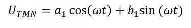
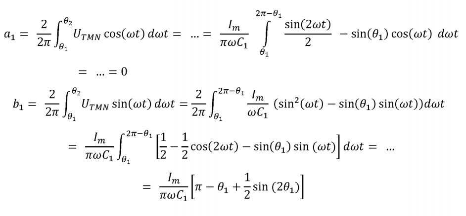
따라서 등가 커패시턴스 C eq 는 다음과 같다:Therefore, the equivalent capacitance C eq is:

동조 가능한 리액턴스 회로의 추가 실시예Additional Embodiments of Tunable Reactance Circuits
도 9는 제2 동조 가능한 리액턴스(904)와 직렬로 결합된 제1 동조 가능한 리액턴스 회로(902)를 포함하는 동조 가능한 리액턴스 회로(900)의 실시예를 도시한다. 회로(902, 904) 각각은 동조 가능한 리액턴스 회로(200)를 포함할 수 있다. 일부 경우에, 예제 리액턴스 회로(900)는 단일 동조 가능한 리액턴스 회로(200) 보다 더 큰 임피던스 범위(예를 들어, 더 큰 리액턴스 범위)를 가능하게 할 수 있다. 이런 식으로, 리액턴스 회로(900)를 채용한 시스템(예를 들어, 주어진 세트의 인버터 및 정류기 제한들을 갖는 무선 전력 시스템)은 (송신기 위치에 대한) 수신기 위치의 더 큰 변화로부터 더 넓은 범위의 결합으로 인해 시스템에 의해 관찰되는 더 넓은 범위의 반사 임피던스에 적응 및/또는 응답할 수 있다. 예를 들어, 동조 가능한 리액턴스 회로(900)를 갖는 무선 전력 송신기(102)는 수신기 위치의 주어진 범위에 걸쳐 더 높은 레벨의 전력을 송신할 수 있고/있거나 동조 가능한 리액턴스 회로가 없는 송신기보다 더 큰 효율로 동작할 수 있다. 다른 예에서, 동조 가능한 리액턴스 회로(900)를 갖는 무선 전력 송신기(102)는 수신기 위치의 주어진 범위에 걸쳐 더 높은 레벨의 전력을 송신할 수 있고/있거나 동조 가능한 리액턴스 회로(200)를 갖는 송신기보다 더 큰 효율로 동작할 수 있다.9 shows an embodiment of a
위의 개념은 도 10a - 10b의 표에 추가로 예시되어 있다. 예를 들어, 도 10a에서, 예시적인 송신기(1002)는 동조 가능한 리액턴스 회로(예를 들어, 200 또는 900)를 갖지 않을 수 있다. 대신, 일부 경우에, 그 자리에 송신기(1002)는 고정 리액턴스 X1을 갖는 컴포넌트(예를 들어, 인덕터 또는 커패시터)를 가질 수 있다. 다른 경우에, 그러한 컴포넌트가 없을 수 있다(이 경우 리액턴스가 제로(0)이다). 예시적인 송신기(1004)는 X2-X3의 리액턴스 범위에 걸쳐 동조 가능한 리액턴스 회로(200)를 가질 수 있다. 예시적인 송신기(1006)는 동조 가능한 리액턴스 회로(200)와 동일한 스위칭 컴포넌트가 회로(900)에서 사용된다고 가정할 때 X2-X3의 두 배인 X4-X5의 리액턴스 범위에 걸쳐 동조 가능한 리액턴스 회로(900)를 가질 수 있다. 동조 가능한 리액턴스 회로(200)가 직렬로 추가되면(예를 들어, 직렬로 3개 회로, 4개 회로, 5개 회로 등), 리액턴스 범위는 비례적으로 증가한다(예를 들어, 단일 동조 가능한 리액턴스 회로(200)의 3배, 4배, 5배 등).The above concept is further illustrated in the tables of FIGS. 10A - 10B. For example, in FIG. 10A , the
도 10a에 제공된 예에서, 임피던스 범위는 서로에 속하며, 예를 들어, 리액턴스 범위 X1-X2는 리액턴스 범위 X3-X4에 속한다. 일부 실시예에서, "내포된(nested)" 리액턴스 범위는 동일한 평균 값을 가질 수 있다. 일부 실시예에서, 리액턴스 범위는 다른 수단을 가질 수 있다. 도 10b를 참조하면, 일부 경우에, 리액턴스 범위가 부분적으로 중첩할 수 있다. 예를 들어, 송신기(1008)의 리액턴스 범위 X1-X2는 리액턴스 범위 X3-X4와 부분적으로 중첩될 수 있고/있거나 리액턴스 범위 X3-X4는 리액턴스 범위 X5-X6과 부분적으로 중첩될 수 있다. 그러나 도 10a - 도 10b는 무선 전력 송신기에 대한 것으로, 무선 전력 수신기에도 동일 또는 유사한 개념이 적용될 수 있다는 것에 유의한다.In the example provided in Fig. 10a, the impedance ranges belong to each other, eg the reactance range X1-X2 belongs to the reactance range X3-X4. In some embodiments, the “nested” reactance ranges may have the same average value. In some embodiments, the reactance range may have other means. Referring to FIG. 10B , in some cases, reactance ranges may partially overlap. For example, reactance range X1-X2 of
일부 실시예에서, 동조 가능한 리액턴스 회로(900)를 활용하는 무선 전력 송신기(102)는 송신기(102)의 전술한 부트스트랩 파워 서플라이와 별개의 전용 절연 DC-DC 컨버터(예를 들어, 인버터(108)의 일부의 전도 동안 충전하도록 구성된 부트스트랩 커패시터)를 활용할 수 있다. 동조 가능한 리액턴스 게이트 드라이버가 전용 절연 DC-DC 컨버터에 의해 전력이 공급되는 경우, 송신기는 구동 회로와 동조 가능한 리액턴스 회로 사이에 결합된 인덕터를 더 포함할 수 있다는 것에 유의한다.In some embodiments,
도 11은 동조 가능한 리액턴스 회로(1102a, 1102b)(집합적으로 회로(1102)로 지칭됨)를 포함하는 무선 전력 송신기의 부분(1100)의 개략도이다. 예시적인 송신기 부분(1100)에서, 단일 스위치 동조 가능한 리액턴스 회로(1102a, 1102b)는 상단 지로 및 하단 지로에 각각 사용된다. 회로(1102a, 1102b)는 인버터(108)와 고정 정합 네트워크(1103) 사이에 결합된다. 두 개의 개별 회로(1102a, 1102b)를 활용함으로써, 원하는 리액턴스가 2개의 지로에 걸쳐 "분할"되어서 송신기에 균형 잡힌 리액턴스를 제공한다. C1= 187nF 및 90°와 180° 사이의 위상각 φ를 사용하는 개별 회로(200)의 예를 참조하며, 대응하는 "분할" 개별 커패시터 (1) C1A1, C1A2(함께 1102a)는 대략 187nF의 총 커패시턴스 값을 갖고, (2) C1B1, C1B2(함께 1102b)는 대략 187nF의 총 커패시턴스 값을 가지므로, 총 직렬 등가 커패시턴스는 93.5nF이다. C1= 187nF 및 0°와 180° 사이의 위상각 φ를 사용하는 개별 회로(200)의 예를 참조하면, 대응하는 "분할" 개별 커패시터 (1) C1A1, C1A2(함께 1102a)는 약 93.5nF의 총 커패시턴스 값을 가지며 (2) C1B1, C1B2(함께 1102b)는 대략 93.5nF의 총 커패시턴스 값을 가지므로, 총 직렬 등가 커패시턴스는 46.75nF이다.11 is a schematic diagram of a
회로(1102a, 1102b)는 별도의 전용 절연 DC-DC 컨버터(1104)에 의해 전력을 공급받을 수 있다. 일부 실시예에서, 회로(1102a, 1102b)는 제어기(1106)에 의해 제어될 수 있다. 제어기(1106)는 제어기(122)의 일부이거나 제어기와 동일할 수 있다. 인버터(108)는 별도의 파워 서플라이(1108)에 의해 전력이 공급되고 별도의 제어기(1110)에 의해 제어될 수 있다. 제어기(1106 및 1110)는 함께 패키징될 수 있고, 서로 연결될 수 있고/있거나 동일한 제어기(예를 들어, 122)의 일부 있다는 것에 유의한다.
일부 실시예에서, 동조 가능한 리액턴스 회로(900)를 활용하는 무선 전력 수신기(104)는 상기에서 설명된 부트스트랩 파워 서플라이(예를 들어, 정류기(118)의 일부의 전도 동안 충전하도록 구성된 부트스트랩 커패시터)과 별개의 절연된 DC-DC 컨버터를 활용할 수 있다. 도 12는 동조 가능한 리액턴스 회로(1202a, 1202b)(집합적으로 회로(1202)로 지칭됨)를 포함하는 무선 전력 수신기의 부분(1200)의 개략도이다. 예시적인 수신기 부분(1200)에서, 단일 스위치 동조 가능한 리액턴스 회로(1202a 및 1202b)는 상단 지로 및 하단 지로에 각각 활용된다. 회로(1202a, 1202b)는 고정 정합 네트워크(1203)와 정류기(118) 사이에 결합된다. 두 개의 개별 회로(1202a, 1202b)를 활용함으로써, 원하는 리액턴스가 2개의 지로에 걸쳐 "분할"되어 수신기에 균형 잡힌 리액턴스를 제공한다. C1=135nF 및 90°와 180° 사이의 위상각 φ를 활용하는 개별 회로(200)의 예를 참조하면, 대응하는 "분할" 개별 커패시터(1) C1A1, C1A2(함께 1202a)는 대략 135nF의 총 커패시턴스 값을 가지며, (2) C1B1, C1B2(함께 1202b)는 대략 135nF의 총 커패시턴스 값을 가지므로, 총 직렬 등가 커패시턴스는 67.5nF이다. C1=135nF 및 0°와 180° 사이의 위상각 φ를 활용하는 개별 회로(200)의 예를 참조하면, 대응하는 "분할" 개별 커패시터 (1) C1A1, C1A2(함께 1202a)는 약 67.5nF의 총 커패시턴스 값을 가지며 (2) C1B1, C1B2(함께 1202b)는 대략 67.5nF의 총 커패시턴스 값을 가지므로 총 직렬 등가 커패시턴스 33.75nF이다.In some embodiments, the
도 13은 동조 가능한 리액턴스 회로(900)를 포함하는 무선 전력 수신기 부분(1300)의 개략도이다. 특히, 상단 지로에서, 수신기 부분(1300)은 제1 동조 가능 리액턴스 서브회로(1302a) 및 제2 동조 가능 리액턴스 서브회로(1304a)를 포함한다. 서브회로(1302a)의 스위치는 게이트 저항기(1306a)에 결합된다. 서브회로(1304b)의 스위치는 고전압 디커플링(decoupling) 다이오드 Dga, 게이트 저항기 Rg2a, 및 풀다운(pull-down) 저항기 Rgsa를 포함하는 게이트 회로(1308a)에 결합된다. 저항기(1306a) 및 게이트 회로(1308a)의 입력은 부트스트랩 회로(1312a)에 의해 전력을 공급받는 레벨 편이 게이트 드라이버(level-shifting gate driver)(1310a)의 출력에 결합된다. 부트스트랩 회로(1312a)는 정류기(118)의 입력에 결합된다.13 is a schematic diagram of a wireless
하단 지로에서, 수신기 부분(1300)은 제1 조정가능 리액턴스 서브회로(1302b) 및 제2 조정가능 리액턴스 서브회로(1304b)를 포함한다. 서브회로(1302b)의 스위치는 게이트 저항기(1306b)에 결합된다. 서브회로(1304b)의 스위치는 고전압 디커플링 다이오드 Dgb, 게이트 저항기 Rg2b, 및 풀다운 저항기 Rgsb를 포함하는 게이트 회로(1308b)에 결합된다. 저항기(1306b) 및 게이트 회로(1308b)의 입력은 부트스트랩 회로(1312a)에 의해 전력을 공급받는 편이 게이트 드라이버(shifting gate driver)(1310b)의 출력에 결합된다. 부트스트랩 회로(1312a)는 정류기(118)의 입력에 결합된다.In the lower branch,
도 14a 내지 도 14d는 수신기 부분(1300)의 다양한 신호를 예시한다. 도 14a를 참조하면, 게이트 회로(1308a, 1308b)에서, 고전압 디커플링 다이오드 전압(1402)은 제1 조정가능 리액턴스 서브회로(1302a, 1302b)에 걸친 전압을 각각 차단한다. 도 14b에서, 고전압 디커플링 다이오드 전류(1404)는 FET 커패시턴스를 충전하기 위한 초기 피크(1406)를 가지며, 그런 다음, 피크(1406) 이후의 시간(1408) 동안, 온-타임 동안 게이트 저항기 플러스 풀다운(pull-down) 저항기에 의해 나누어진 게이트 구동 전압과 동일하다. 회로(1312a)의 각각의 부트스트랩 커패시터(Cba) 또는 회로(1312b)의 부트스트랩 커패시터(Cbb)는 이 전류가 게이트 구동 전압을 저하시키지 않도록 충분히 크게 구성된다. 도 14c에서, 동조 가능한 리액턴스 서브회로(1308a 또는 1308b)의 FET의 결과적인 게이트-소스 전압(1410)은 빠른 상승 시간(1412) 및 FET 게이트-소스 커패시턴스 및 풀다운 저항기에 기초한 수동 방전을 갖는다. 도 14d에서, 동조 가능한 리액턴스 서브회로(1308a 또는 1308b)의 FET의 결과적인 드레인-소스 전압(1414)은 동조 가능한 리액턴스 서브회로(1306a 또는 1306b)의 FET의 드레인-소스 전압과 거의 동일하여 리액턴스를 효과적으로 두 배로 증가시킨다.14A-14D illustrate various signals of the
도 15a 내지 도 15d는 수신기 부분(1300)의 다양한 신호를 예시한다. 도 15a는 동조 가능한 리액턴스 네트워크(예를 들어, 200, 900, 1302a, 1304a)로의 전류 I(Na)를 예시한다. 도 15b에서, 동조 가능한 리액턴스 서브회로(1302a 또는 1302b)의 FET 양단의 드레인-소스 전압(1502)은 단일 스위치 동조 가능한 리액턴스 회로(200)와 동일하다. 도 15c에서, FET의 드레인-소스 전압(1504) 동조 가능한 리액턴스 하위 회로(1304a 또는 1304bis)의 동조 가능한 리액턴스 하위 회로(1302a 또는 1302b)의 FET의 드레인-소스 전압은 각각 거의 동일하다. 도 15d를 참조하면, 직렬 동조 가능 리액턴스 서브회로(1302a 및 1304a)(또는 1302b 및 1304b)의 각 지로에 걸친 결과적인 총 직렬 전압은 단일 스위치 동조 가능 리액턴스 구현(200)의 거의 두 배이며, 리액턴스를 효과적으로 두 배로 만든다.15A-15D illustrate various signals of the
도 16a는 동조 가능한 리액턴스 서브회로(1302a, 1304a)를 갖는 상단 지로 및 동조 가능한 리액턴스 서브회로들(1302b, 1304b)을 갖는 하단 지로를 포함하는, 수신기 부분(1300)의 각각의 지로에 걸친 총 직렬 전압을 나타내는 5개의 신호들(1602, 1604, 1606, 1608, 1610), 예를 들어 90°와 180° 사이의 5개의 예시적인 위상 각도들 φ의 플롯이다. 5개의 상이한 위상각이 아래 표 1에 제공된다. 위상각 φ가 90에서 180으로 증가함에 따라 전압도 증가한다. 도 16b는 동조 가능한 리액턴스 서브회로(1302a, 1304a)을 갖는 상단 지로 및 동조 가능한 리액턴스 서브회로들(1302b, 1304b)을 갖는 하단 지로를 포함하는, 수신기 부분(1300)의 각각의 지로에 걸친 총 직렬 전압을 나타내는 5개의 신호들, 예를 들어 0°와 180° 사이의 5개의 예시적인 위상 각도들 φ의 플롯이다. 5개의 상이한 위상각이 아래 표 2에 제공된다. 위상각 φ가 0에서 180으로 증가함에 따라 전압도 증가한다.16A shows the total series across each branch of
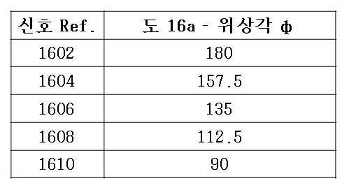
표 1. 도 16a의 전압 신호에 대한 90°와 180° 사이의 위상각 φ.Table 1. Phase angle φ between 90° and 180° for the voltage signal in FIG. 16A.

표 2. 도 16b의 전압 신호에 대한 0°와 180° 사이의 위상각 φ.Table 2. Phase angle φ between 0° and 180° for the voltage signal in FIG. 16B.
하드웨어 및 소프트웨어구현Hardware and software implementation
도 17은 본 명세서에 설명된 시스템 및 방법을 구현하는데 사용될 수 있는 예시적인 컴퓨터 시스템(1700)의 블록도이다. 범용 컴퓨터, 네트워크 기기, 모바일 디바이스, 또는 다른 전자 시스템은 또한 시스템(1700)의 적어도 일부를 포함할 수 있다. 시스템(1700)은 프로세서(1710), 메모리(1720), 저장 디바이스(1730), 및 입력/출력 디바이스(1740)를 포함한다. 컴포넌트(1710, 1720, 1730, 1740) 각각은 예를 들어, 시스템 버스(1750)를 사용하여 상호 연결될 수 있다. 프로세서(1710)는 시스템(1700) 내에서 실행을 위한 명령들을 처리할 수 있다. 일부 구현예들에서, 프로세서(1710)는 단일 스레드(single-threaded) 프로세서이다. 일부 구현예들에서, 프로세서(1710)는 멀티 스레드(multi-threaded) 프로세서이다. 프로세서(1710)는 메모리(1720) 또는 저장 디바이스(1730)에 저장된 명령들을 처리할 수 있다.17 is a block diagram of an
메모리(1720)는 시스템(1700) 내에 정보를 저장한다. 일부 구현예들에서, 메모리(1720)는 비일시적 컴퓨터 판독가능 매체이다. 일부 구현예들에서, 메모리(1720)는 휘발성 메모리 유닛이다. 일부 구현예들에서, 메모리(1720)는 비휘발성 메모리 유닛이다. 일부 예에서, 상기에서 설명된 데이터의 일부 또는 전부는 개인용 컴퓨팅 디바이스, 하나 이상의 중앙 집중식 컴퓨팅 디바이스에서 호스팅되는 데이터 저장소에, 또는 클라우드 기반 저장소를 통해 저장될 수 있다. 일부 예에서 일부 데이터는 한 위치에 저장되고, 다른 데이터는 다른 위치에 저장된다. 일부 예에서 양자 컴퓨팅이 사용될 수 있다. 일부 예에서는 함수형 프로그래밍 언어를 사용할 수 있다. 일부 예에서, 플래시 기반 메모리와 같은 전기 메모리가 사용될 수 있다.Memory 1720 stores information within
저장 디바이스(1730)는 시스템(1700)을 위한 대용량 저장 디바이스를 제공할 수 있다. 일부 구현예에서, 저장 디바이스(1730)는 비일시적 컴퓨터 판독 가능 매체이다. 다양한 상이한 구현예들에서, 저장 디바이스(1730)는, 예를 들어, 하드 디스크 디바이스, 광 디스크 디바이스, 솔리드-데이트 드라이브, 플래시 드라이브, 또는 일부 다른 대용량 저장 디바이스를 포함할 수 있다. 예를 들어, 저장 디바이스는 장기 데이터(예를 들어, 데이터베이스 데이터, 파일 시스템 데이터 등)를 저장할 수 있다. 입력/출력 디바이스(1740)는 시스템(1700)에 대한 입력/출력 동작을 제공한다. 일부 구현예에서, 입력/출력 디바이스(1740)는 하나 이상의 네트워크 인터페이스 디바이스, 예를 들어 이더넷 카드, 직렬 통신 디바이스, 예를 들어, RS-232 포트 및/또는 무선 인터페이스 디바이스 예를 들어, 802.11 카드, 3G 무선 모뎀 또는 4G 무선 모뎀을 포함할 수 있다. 일부 구현예에서, 입력/출력 디바이스는 입력 데이터를 수신하고 출력 데이터를 다른 입력/출력 디바이스, 예를 들어, 키보드, 프린터 및 디스플레이 디바이스(1760)로 발송하도록 구성된 드라이버 디바이스를 포함할 수 있다. 일부 예에서, 모바일 컴퓨팅 디바이스, 모바일 통신 디바이스, 기타 디바이스가 사용될 수 있다.
일부 구현예에서, 상기에서 설명된 접근 방식의 적어도 일부는 실행 시 하나 이상의 처리 디바이스가 상기에서 설명된 프로세스 및 기능을 수행하게 하는 명령에 의해 실현될 수 있다. 이러한 명령은 예를 들어, 스크립트 명령 또는 실행 코드와 같은 해석된 명령, 또는 비일시적 컴퓨터 판독 가능 매체에 저장된 다른 명령을 포함할 수 있다. 저장 디바이스(1730)는 서버 팜 또는 널리 분산된 서버의 세트와 같은 네트워크를 통해 분산 방식으로 구현되거나 단일 컴퓨팅 디바이스로 구현될 수 있다.In some implementations, at least some of the approaches described above may be realized by instructions that, when executed, cause one or more processing devices to perform the processes and functions described above. Such instructions may include, for example, interpreted instructions such as script instructions or executable code, or other instructions stored on a non-transitory computer readable medium.
예시적인 처리 시스템이 도 17에 설명되었지만, 본 명세서에 설명된 주제, 기능 동작 및 프로세스의 실시예는 본 명세서에 개시된 구조 및 이들의 구조적 등가물, 또는 이들 중 하나 이상의 조합을 포함하는 다른 유형의 디지털 전자 회로부로, 유형적으로 구현된 컴퓨터 소프트웨어 또는 펌웨어로, 컴퓨터 하드웨어로 구현될 수 있다. 본 명세서에 기술된 주제의 실시예는 하나 이상의 컴퓨터 프로그램, 즉, 데이터 처리 장치에 의해 실행되거나 데이터 처리 장치의 동작을 제어하기 위해 유형의 비휘발성 프로그램 캐리어에 인코딩된 컴퓨터 프로그램 명령의 하나 이상의 모듈로 구현될 수 있다. 대안으로 또는 추가로, 프로그램 명령은 인공적으로 생성된 전파 신호, 예를 들어, 데이터 처리 장치에 의한 실행을 위해 적절한 수신기 디바이스로의 송신을 위한 정보를 인코딩하기 위해 생성되는 기계 생성 전기, 광학 또는 전자기 신호에 인코딩될 수 있다. 컴퓨터 저장 매체는 기계 판독 가능 저장 디바이스, 기계 판독 가능 저장 기판, 랜덤 또는 직렬 액세스 메모리 디바이스, 또는 이들 중 하나 이상의 조합일 수 있다.While an exemplary processing system is illustrated in FIG. 17 , embodiments of the subject matter, functional operations, and processes described herein may be useful for other types of digital devices, including the structures disclosed herein and their structural equivalents, or combinations of one or more thereof. It may be implemented as electronic circuitry, as tangibly implemented computer software or firmware, or as computer hardware. Embodiments of the subject matter described herein may be directed to one or more modules of computer programs, i.e., computer program instructions executed by a data processing device or encoded in a tangible, non-volatile program carrier for controlling the operation of a data processing device. can be implemented Alternatively or additionally, the program instructions may be artificially generated radio signals, e.g. machine generated electrical, optical or electromagnetic generated to encode information for transmission to a suitable receiver device for execution by a data processing apparatus. can be encoded into the signal. A computer storage medium may be a machine-readable storage device, a machine-readable storage substrate, a random or serial access memory device, or a combination of one or more of these.
용어 "시스템"은 예를 들어, 프로그램 가능한 프로세서, 컴퓨터, 또는 다수의 프로세서 또는 컴퓨터를 포함하여 데이터를 처리하기 위한 모든 종류의 장치, 디바이스 및 기계를 포함할 수 있다. 처리 시스템은 FPGA(field programmable gate array) 또는 ASIC(application specific integrated circuit)과 같은 특수 목적 논리 회로부를 포함할 수 있다. 처리 시스템은 하드웨어에 추가하여, 해당 컴퓨터 프로그램에 대한 실행 환경을 생성하는 코드, 예를 들어, 프로세서 펌웨어, 프로토콜 스택, 데이터베이스 관리 시스템, 운영 체제 또는 이들 중 하나 이상의 조합을 구성하는 코드를 포함할 수 있다.The term "system" may include all kinds of apparatus, devices and machines for processing data including, for example, a programmable processor, a computer, or multiple processors or computers. The processing system may include special purpose logic circuitry such as a field programmable gate array (FPGA) or application specific integrated circuit (ASIC). A processing system may include, in addition to hardware, code that creates an execution environment for a corresponding computer program, such as code that makes up a processor firmware, a protocol stack, a database management system, an operating system, or a combination of one or more of these. there is.
컴퓨터 프로그램(프로그램, 소프트웨어, 소프트웨어 애플리케이션, 모듈, 소프트웨어 모듈, 스크립트 또는 코드라고도 함)은 컴파일되거나 해석된 언어, 또는 선언적 또는 절차적 언어를 포함하는 모든 형태의 프로그래밍 언어로 기록될 수 있고, 독립 실행형 프로그램으로서 또는 컴퓨팅 환경에서 사용하기에 적합한 모듈, 컴포넌트, 서브루틴 또는 다른 유닛으로서 임의의 형태로 배치될 수 있다. 컴퓨터 프로그램은 파일 시스템의 파일에 대응할 수 있지만 반드시 그런 것은 아니다. 프로그램은 다른 프로그램 또는 데이터를 보유하는 파일의 일부(예를 들어, 마크업 언어 문서에 저장된 하나 이상의 스크립트), 해당 프로그램에 전용된 단일 파일, 또는 다수의 조정된 파일(예를 들어, 하나 이상의 모듈, 서브 프로그램, 또는 코드의 일부를 저장하는 파일)에 저장될 수 있다. 컴퓨터 프로그램은 하나의 컴퓨터 또는 한 사이트에 위치되거나 다수의 사이트에 분산되고 통신 네트워크로 상호 연결된 다수의 컴퓨터 상에서 실행되도록 배치될 수 있다.A computer program (also referred to as a program, software, software application, module, software module, script, or code) may be written in any form of programming language, including compiled or interpreted language, or declarative or procedural language, and may be independently executed. deployed in any form as a type program or as a module, component, subroutine or other unit suitable for use in a computing environment. Computer programs can, but not necessarily, correspond to files in a file system. A program may be part of a file holding other programs or data (for example, one or more scripts stored in a markup language document), a single file dedicated to that program, or a number of coordinated files (for example, one or more modules). , a subprogram, or a file that stores part of the code). A computer program may be deployed to be executed on one computer or on multiple computers located at one site or distributed across multiple sites and interconnected by a communication network.
본 명세서에 설명된 프로세스 및 논리 흐름은 입력 데이터에 대해 동작하고 출력을 생성함으로써 기능을 수행하기 위해 하나 이상의 컴퓨터 프로그램을 실행하는 하나 이상의 프로그래밍 가능한 컴퓨터에 의해 수행될 수 있다. 프로세스 및 논리 흐름은 또한 특수 목적 논리 회로부 예를 들어, FPGA(field programmable gate array) 또는 ASIC(application specific integrated circuit)에 의해 수행될 수 있고 장치도 이들로서 구현될 수 있다.The processes and logic flows described herein can be performed by one or more programmable computers executing one or more computer programs to perform functions by operating on input data and generating output. The processes and logic flows may also be performed by special purpose logic circuitry, such as a field programmable gate array (FPGA) or an application specific integrated circuit (ASIC), and devices may be implemented as such.
컴퓨터 프로그램의 실행에 적합한 컴퓨터는 예를 들어, 범용 또는 특수 목적 마이크로프로세서 또는 둘 모두, 또는 임의의 다른 종류의 중앙 처리 유닛을 포함할 수 있다. 일반적으로, 중앙 처리 유닛은 판독 전용 메모리나 랜덤 액세스 메모리 또는 둘 모두에서 명령과 데이터를 수신할 것이다. 컴퓨터는 일반적으로 명령을 수행하거나 실행하기 위한 중앙 처리 유닛과 명령 및 데이터를 저장하기 위한 하나 이상의 메모리 디바이스를 포함한다. 일반적으로, 컴퓨터는 또한 데이터를 저장하기 위한 하나 이상의 대용량 저장 디바이스, 예를 들어 자기, 광자기 디스크 또는 광 디스크로부터 데이터를 수신하거나 이들로 데이터를 전송하거나 둘 모두를 포함하거나 데이터를 수신, 전송 또는 둘 모두를 위해 작동 가능하게 결합된다. 그러나 컴퓨터는 이러한 디바이스를 필요로 하지 않는다. 더욱이 컴퓨터는 다른 디바이스 예컨대, 몇 가지를 들자면, 휴대전화, PDA(Personal Digital Assistant), 모바일 오디오 또는 비디오 플레이어, 게임 콘솔, GPS(Global Positioning System) 수신기 또는 휴대용 저장 디바이스(예를 들어, USB(범용 직렬 버스) 플래시 드라이브)에 내장될 수 있다.A computer suitable for the execution of a computer program may include, for example, a general purpose or special purpose microprocessor or both, or any other type of central processing unit. Typically, a central processing unit will receive instructions and data from either read-only memory or random access memory or both. A computer generally includes a central processing unit for carrying out or executing instructions and one or more memory devices for storing instructions and data. In general, a computer also receives data from, transmits data to, or includes or receives, transmits, or receives data from one or more mass storage devices for storing data, such as magnetic, magneto-optical, or optical disks. operatively coupled for both. However, computers do not need these devices. Moreover, a computer can be used as another device such as a cell phone, a personal digital assistant (PDA), a mobile audio or video player, a game console, a Global Positioning System (GPS) receiver, or a portable storage device (e.g., a USB (universal), to name a few). serial bus) can be embedded in a flash drive).
컴퓨터 프로그램 명령 및 데이터를 저장하기에 적합한 컴퓨터 판독 가능 매체는 예를 들어 EPROM, EEPROM 및 플래시 메모리 디바이스와 같은 반도체 메모리 디바이스; 자기 디스크, 예를 들어, 내부 하드 디스크 또는 이동식 디스크; 자기 광 디스크; 및 CD-ROM 및 DVD-ROM 디스크를 포함하는 모든 형태의 비휘발성 메모리, 매체 및 메모리 디바이스를 포함한다. 프로세서와 메모리는 특수 목적 논리 회로부에 의해 보완되거나 통합될 수 있다.Computer readable media suitable for storing computer program instructions and data include, for example, semiconductor memory devices such as EPROM, EEPROM and flash memory devices; magnetic disks such as internal hard disks or removable disks; magnetic optical disk; and all forms of non-volatile memory, media and memory devices including CD-ROM and DVD-ROM disks. The processor and memory may be complemented or integrated by special purpose logic circuitry.
본 명세서에 설명된 주제의 실시예는 예를 들어, 데이터 서버와 같은 백엔드 컴포넌트를 포함하거나 예를 들어, 애플리케이션 서버와 같은 미들웨어 컴포넌트를 포함하거나 프론트엔드 컴포넌트 예를 들어, 사용자가 본 명세서에 설명된 주제의 구현예와 상호 작용할 수 있는 그래픽 사용자 인터페이스 또는 웹 브라우저를 갖는 클라이언트 컴퓨터를 포함하거나, 또는 하나 이상의 이러한 백엔드, 미들웨어 또는 프론트 엔드 컴포넌트의 임의의 조합을 포함하는 컴퓨팅 시스템에서 구현될 수 있다. 시스템의 컴포넌트는 통신 네트워크와 같은 디지털 데이터 통신의 임의의 형태 또는 매체에 의해 상호 연결될 수 있다. 통신 네트워크의 예는 근거리 통신망("LAN") 및 광역 통신망("WAN"), 예를 들어 인터넷을 포함한다.Embodiments of the subject matter described herein may include a backend component, eg, a data server, or include a middleware component, eg, an application server, or a frontend component, eg, a user described herein. It may be implemented on a computing system that includes a client computer having a graphical user interface or web browser capable of interacting with implementations of the subject matter, or that includes any combination of one or more of these backend, middleware, or frontend components. Components of the system may be interconnected by any form or medium of digital data communication, such as a communication network. Examples of communication networks include local area networks ("LAN") and wide area networks ("WAN"), such as the Internet.
컴퓨팅 시스템은 클라이언트와 서버를 포함할 수 있다. 클라이언트와 서버는 일반적으로 서로 멀리 떨어져 있으며, 전형적으로 통신 네트워크를 통해 상호 작용한다. 클라이언트와 서버의 관계는 각각의 컴퓨터에서 실행되고 서로 클라이언트-서버 관계를 갖는 컴퓨터 프로그램 덕분에 발생한다.A computing system may include a client and a server. Clients and servers are generally remote from each other and typically interact through a communication network. The relationship of client and server arises by virtue of computer programs running on the respective computers and having a client-server relationship to each other.
본 명세서는 많은 특정 구현 세부사항을 포함하지만, 이들은 청구될 수 있는 범위에 대한 제한으로 해석되어서는 안 되며 오히려 특정 실시예에 특정될 수 있는 특징부의 설명으로 해석되어야 한다. 별도의 실시예와 관련하여 본 명세서에 설명된 특정 특징부는 단일 실시예에서 조합하여 구현될 수도 있다. 역으로, 단일 실시예의 맥락에서 설명된 다양한 특징부는 또한 개별적으로 또는 임의의 적절한 서브 조합으로 다수의 실시예에서 구현될 수 있다. 더욱이, 특징부가 특정 조합으로 작용하는 것으로 위에서 설명될 수 있고 심지어 초기에 그렇게 청구될 수도 있지만, 청구된 조합의 하나 이상의 특징부가 일부 경우에 조합에서 제거될 수 있고 청구된 조합은 서브 조합으로 또는 서브 조합의 변형에 관한 것일 수 있다.Although this specification contains many specific implementation details, they should not be construed as limitations on the scope of what may be claimed, but rather as descriptions of features that may be specific to a particular embodiment. Certain features that are described in this specification in the context of separate embodiments may also be implemented in combination in a single embodiment. Conversely, various features that are described in the context of a single embodiment can also be implemented in multiple embodiments separately or in any suitable subcombination. Moreover, while features may be described above as acting in particular combinations and may even be initially claimed as such, one or more features of a claimed combination may in some cases be removed from the combination and the claimed combination may be in a subcombination or in a subcombination. It may be about the transformation of
유사하게, 동작들이 도면에 특정 순서로 도시되어 있지만, 이는 바람직한 결과를 달성하기 위해 그러한 동작이 도시된 특정 순서 또는 순차적인 순서로 수행되거나 도시된 모든 동작이 수행되어야 함을 요구하는 것으로 이해되어서는 안 된다. 특정 상황에서는 멀티 태스킹과 병렬 처리가 유리할 수 있다. 더욱이, 상기에서 설명된 실시예에서 다양한 시스템 컴포넌트의 분리는 모든 실시예에서 그러한 분리를 요구하는 것으로 이해되어서는 안 되며, 설명된 프로그램 컴포넌트 및 시스템은 일반적으로 단일 제품으로 함께 통합되거나 여러 제품으로 패키징될 수 있음을 이해해야 한다.Similarly, while actions are shown in a particular order in the drawings, this should not be construed as requiring that such acts be performed in the particular order or sequential order shown, or that all acts shown be performed in order to achieve a desired result. Can not be done. Multitasking and parallel processing can be advantageous in certain circumstances. Moreover, the separation of various system components in the embodiments described above should not be understood as requiring such separation in all embodiments, and the described program components and systems are generally integrated together into a single product or packaged into multiple products. You have to understand that it can be.
주제의 특정 실시예가 설명되었다. 다른 실시예는 다음 청구항의 범위 내에 있다. 예를 들어, 청구항에 언급된 액션들은 상이한 순서로 수행될 수 있으며 여전히 바람직한 결과를 달성할 수 있다. 일 예로서, 첨부 도면에 도시된 프로세스는 바람직한 결과를 달성하기 위해 도시된 특정 순서 또는 순차적인 순서를 반드시 필요로 하는 것은 아니다. 특정 구현예에서, 멀티 태스킹 및 병렬 처리가 유리할 수 있다. 설명된 프로세스에서 다른 단계 또는 스테이지가 제공되거나 단계 또는 스테이지가 제거될 수 있다. 따라서, 다른 구현예는 다음 청구항의 범위 내에 있다.Specific embodiments of the subject matter have been described. Other embodiments are within the scope of the following claims. For example, the actions recited in the claims can be performed in a different order and still achieve desirable results. As an example, the processes depicted in the accompanying figures do not necessarily require the specific order shown or sequential order to achieve desirable results. In certain implementations, multitasking and parallel processing may be advantageous. Other steps or stages may be provided or steps or stages may be eliminated in the described process. Accordingly, other implementations are within the scope of the following claims.
용어Terms
본 명세서에 사용된 어구 및 용어는 설명을 위한 것이며 제한하는 것으로 간주되어서는 안 된다.The phraseology and terminology used herein is for descriptive purposes and should not be regarded as limiting.
명세서 및 청구범위에 사용된 용어 "대략", 문구 "대략적으로 동일" 및 다른 유사한 문구(예를 들어, "X는 대략 Y의 값을 갖는다" 또는 "X는 대략 Y와 동일하다")는 하나의 값(X)이 다른 값(Y)의 미리 결정된 범위 내에 있음을 의미하는 것으로 이해되어야 한다. 미리 결정된 범위는 달리 표시되지 않는 한 플러스 또는 마이너스 20%, 10%, 5%, 3%, 1%, 0.1%, 또는 0.1% 미만일 수 있다.As used in the specification and claims, the term "approximately", the phrase "approximately equal to" and other similar phrases (e.g., "X has a value of approximately Y" or "X equals approximately Y") mean one It should be understood to mean that the value (X) of is within a predetermined range of other values (Y). The predetermined range may be plus or minus 20%, 10%, 5%, 3%, 1%, 0.1%, or less than 0.1% unless otherwise indicated.
명세서 및 청구범위에 사용된 부정관사 "a" 및 "an"은 명백하게 반대로 표시되지 않는 한 "적어도 하나"를 의미하는 것으로 이해되어야 한다. 명세서 및 청구범위에 사용된 문구 "및/또는 그렇게 결합된 요소, 즉 일부 경우에 결합적으로 존재하고, 다른 경우에 분리적으로 존재하는 요소의 "어느 하나 또는 둘 모두"를 의미하는 것으로 이해되어야 한다. "및/또는"으로 나열된 다수의 요소는 동일한 방식으로 즉, 그렇게 결합된 요소 중 "하나 이상"으로 해석되어야 한다. "및/또는" 절에 의해 구체적으로 식별된 요소 외에, 구체적으로 식별된 요소들과 관련되거나 관련되지 않은 다른 요소가 선택적으로 존재할 수 있다. 따라서, 비제한적인 예로서, "A 및/또는 B"에 대한 언급은 "포함하는"과 같은 개방형 언어와 함께 사용될 때, 일 실시예에서 A만을 (선택적으로 B 이외의 요소를 포함함); 다른 실시예에서, B만을 (선택적으로 A 이외의 요소를 포함함); 또 다른 실시예에서, A 및 B 둘 모두 (선택적으로 다른 요소를 포함함); 등을 지칭할 수 있다.As used in the specification and claims, the indefinite articles “a” and “an” should be understood to mean “at least one” unless clearly indicated to the contrary. The phrase "and/or" as used in the specification and claims should be understood to mean "either or both" of the elements so conjoined, i.e., present jointly in some cases and separately present in other cases. Multiple elements listed with "and/or" shall be construed in the same manner, i.e., as "one or more" of the elements so conjoined. Other elements may optionally be present, either related or unrelated to the elements described in. Thus, as a non-limiting example, reference to "A and/or B" when used in conjunction with open-ended language such as "comprising": In one embodiment, only A (optionally including elements other than B); in another embodiment, only B (optionally including elements other than A); in yet another embodiment, both A and B (optionally (including other elements); and the like.
명세서 및 청구범위에서 사용된 "또는"은 위에서 정의된 "및/또는"과 동일한 의미를 갖는 것으로 이해되어야 한다. 예를 들어, 목록에서 항목을 분리할 때 "또는" 또는 "및/또는"은 포괄적 즉, 요소들의 수 또는 목록 중 적어도 하나를 포함하지만 하나 이상을 또한 포함하고, 선택적으로, 추가적인 열거되지 않은 항목들을 포함하는 것으로 해석되어야 한다. "단지 하나" 또는 "정확히 하나"와 같이, 반대로 명확하게 표시된 용어들만이, 또는 청구항들에서 사용될 때, "이루어진"은, 요소들의 수 또는 목록 중 정확히 하나의 요소를 포함하는 것을 지칭할 것이다. 일반적으로 사용된 용어 "또는"은 "어느 하나", "중 하나", "중 하나만" 또는 "정확히 하나"와 같은 배타성 용어에 의해 선행될 때 배타적 대안(즉, "어느 하나 또는 다른 하나, 둘 모두는 아님")을 나타내는 것으로 해석되어야 한다. 청구범위에서 사용될 때 "필수적으로 구성되는 것"은 특허법 분야에서 사용되는 통상적인 의미를 갖는다.As used in the specification and claims, “or” should be understood to have the same meaning as “and/or” as defined above. For example, "or" or "and/or" when separating items from a list is inclusive, that is, includes at least one of the number or list of elements but also includes one or more, and optionally additional unlisted items. should be construed as including Only terms explicitly indicated to the contrary, such as "only one" or "exactly one", or when used in the claims, "consisting of" shall refer to the inclusion of exactly one element of a number or list of elements. The commonly used term "or" is an exclusive alternative (i.e., "either one or the other, two but not all"). As used in the claims, “consisting essentially of” has its ordinary meaning as used in the field of patent law.
명세서 및 청구범위에 사용된, 하나 이상의 요소의 목록과 관련하여 "적어도 하나의"라는 문구는 목록의 요소 중 임의의 하나 이상의 요소로부터 선택된 하나 이상의 요소, 그러나 요소 목록에 구체적으로 나열된 각각의 모든 요소 중 적어도 하나를 반드시 포함해야 하는 것은 아니며 요소 목록 내의 요소의 임의의 조합을 제외할 필요는 없는 것을 의미하는 것으로 이해되어야 한다. 이 정의는 또한 "적어도 하나"라는 문구가 언급하는 요소 목록 내에서 구체적으로 식별된 요소 이외에, 구체적으로 식별된 요소와 관련되거나 관련되지 않은 요소가 선택적으로 존재할 수 있음을 허용한다. 따라서, 비제한적인 예로서, "A 및 B 중 적어도 하나"(또는 동등하게 "A 또는 B 중 적어도 하나", 또는 동등하게 "A 및/또는 B 중 적어도 하나")는 한 실시예에서, B가 존재하지 않고 (선택적으로 B 이외의 요소를 포함함) 하나 초과의 A를 선택적으로 포함하는 적어도 하나; 또 다른 실시예에서, A가 존재하지 않고 (선택적으로 A 이외의 요소를 포함함) 하나 초과의 B를 선택적으로 포함하는 적어도 하나; 또 다른 실시예에서, 선택적으로 하나 초과의 A, 및 선택적으로 하나 초과의 B를 포함하는(그리고 선택적으로 다른 요소들을 포함하는) 적어도 하나를 지칭할 수 있다.As used in the specification and claims, the phrase "at least one" in reference to a list of one or more elements means one or more elements selected from any one or more of the elements in the list, but each and every element specifically listed in the list of elements. It should be understood that it does not necessarily include at least one of the elements and does not necessarily exclude any combination of elements in the element list. This definition also permits that, in addition to the elements specifically identified within the list of elements to which the phrase “at least one” refers, there may optionally be elements that may be related or unrelated to the elements specifically identified. Thus, as a non-limiting example, “at least one of A and B” (or equivalently “at least one of A or B”, or equivalently “at least one of A and/or B”) in one embodiment means that B is absent (optionally including elements other than B) and at least one optionally including more than one A; In another embodiment, at least one, optionally including more than one B, with no A present (optionally including elements other than A); In another embodiment, may refer to at least one that optionally includes more than one A, and optionally more than one B (and optionally includes other elements).
"포함하는", "구성하는", "갖는", "함유하는", "수반하는" 및 이들의 변형의 사용은 이후에 나열된 항목 및 추가 항목을 포괄하는 의미이다.The use of "comprising", "comprising", "having", "including", "involving" and variations thereof is meant to encompass the items listed thereafter and additional items.
청구 요소를 수정하기 위한 청구범위에서 "제1", "제2", "제3" 등과 같은 서수 용어의 사용은 그 자체로 하나의 청구 요소가 다른 청구 요소보다 우선권, 우선 순위 또는 순서 또는 방법의 작용이 수행되는 시간적 순서를 의미하지 않는다. 서수 용어는 단지 특정 이름을 가진 하나의 청구 요소를 동일한 이름을 가진 다른 요소(그러나 서수 용어의 사용을 위한)와 구별하여 청구 요소를 구별하기 위한 라벨로서 사용된다.The use of ordinal terms, such as "first," "second," "third," etc., in the claims to modify a claim element, per se gives priority, priority, or order or manner in which one claim element takes precedence over another. does not imply the chronological order in which the actions of An ordinal term is only used as a label to distinguish a claim element by distinguishing one claim element having a particular name from another element having the same name (but for the use of an ordinal term).
Claims (20)
전력이 공급될 때(energized) 제1 용량성 리액턴스와 제2 용량성 리액턴스 사이에서 연속적으로 또는 이산적으로 동조 가능한 용량성 리액턴스를 제시하도록 구성된 적어도 하나의 동조 가능한 리액턴스 회로를 포함하고, 각각의 회로는,
게이트 드라이버에 의해 제어되도록 구성된 스위치 - 상기 게이트 드라이버는 상기 스위치의 온-타임(on-time)을 나타내는 제어 신호를 수신하도록 구성됨 -;
상기 스위치에 역병렬로 결합된 다이오드; 및
상기 다이오드에 병렬로 결합된 하나 이상의 커패시터
를 포함하고,
상기 동조 가능한 용량성 리액턴스는 상기 스위치의 온-타임 및 상기 하나 이상의 커패시터의 총 커패시턴스 값에 기초하는, 시스템.As a system,
at least one tunable reactance circuit configured to present a continuously or discretely tunable capacitive reactance between the first capacitive reactance and the second capacitive reactance when energized, wherein each circuit Is,
a switch configured to be controlled by a gate driver, the gate driver configured to receive a control signal indicative of an on-time of the switch;
a diode coupled in anti-parallel to the switch; and
One or more capacitors coupled in parallel to the diode
including,
wherein the tunable capacitive reactance is based on an on-time of the switch and a total capacitance value of the one or more capacitors.
상기 동조 가능한 리액턴스 회로의 커패시턴스 값 Ceq는,
에 의해 정의되고, 여기서, Ctotal은 총 커패시턴스 값이고, φ는 (i) 90°와 180° 사이 또는 (ii) 0°와 180° 사이의 위상각(phase angle)이며, 상기 스위치의 온-타임은 상기 위상각을 기반으로 하는, 시스템.The method of claim 1,
The capacitance value C eq of the tunable reactance circuit is
where C total is the total capacitance value, φ is the phase angle between (i) 90° and 180° or (ii) 0° and 180°, and the on- Time is based on the phase angle.
상기 스위치는 MOSFET이고, 상기 다이오드는 상기 MOSFET의 바디 다이오드(body diode)인, 시스템.The method of claim 1,
wherein the switch is a MOSFET and the diode is a body diode of the MOSFET.
동작 주파수에서 구동 신호를 출력하도록 구성된 구동 회로 - 상기 구동 회로는 상기 동조 가능한 리액턴스 회로의 입력에 결합된 제1 출력 노드를 가짐 -; 및
상기 구동 신호에 기초하여 전자기장을 생성하도록 구성된 공진기 - 상기 공진기는 상기 동조 가능한 리액턴스 회로의 출력에 결합된 제1 입력 노드를 가짐 - 를 더 포함하는, 시스템.The method of claim 1,
a drive circuit configured to output a drive signal at an operating frequency, the drive circuit having a first output node coupled to an input of the tunable reactance circuit; and
and a resonator configured to generate an electromagnetic field based on the drive signal, the resonator having a first input node coupled to an output of the tunable reactance circuit.
상기 구동 회로는 인버터이고, 상기 시스템은,
상기 인버터의 하나 이상의 게이트 드라이버 및 상기 동조 가능한 리액턴스 회로의 게이트 드라이버에 전력을 공급하도록 구성된 보조 전원을 더 포함하는, 시스템.The method of claim 4,
The drive circuit is an inverter, and the system comprises:
and an auxiliary power supply configured to supply power to at least one gate driver of the inverter and a gate driver of the tunable reactance circuit.
상기 적어도 하나의 동조 가능한 리액턴스 회로는 제1 동조 가능한 리액턴스 회로 및 제2 동조 가능한 리액턴스 회로를 포함하고, 그리고
상기 구동 회로는 상기 제2 동조 가능한 리액턴스 회로의 입력에 결합된 제2 출력 노드를 갖고, 상기 공진기는 상기 제2 동조 가능한 리액턴스 회로의 출력에 결합된 제2 입력 노드를 갖는, 시스템.The method of claim 4,
the at least one tunable reactance circuit includes a first tunable reactance circuit and a second tunable reactance circuit; and
wherein the drive circuit has a second output node coupled to the input of the second tunable reactance circuit, and wherein the resonator has a second input node coupled to the output of the second tunable reactance circuit.
상기 제1 동조 가능한 리액턴스 회로의 커패시턴스 값은 상기 제2 동조 가능한 리액턴스 회로의 커패시턴스 값과 동일한, 시스템.The method of claim 6,
wherein the capacitance value of the first tunable reactance circuit is equal to the capacitance value of the second tunable reactance circuit.
상기 동조 가능한 리액턴스 회로의 입력에 결합된 제1 출력 노드를 갖는 공진기; 및
상기 동조 가능한 리액턴스 회로의 출력에 결합된 제1 입력 노드를 갖는 정류기를 더 포함하는, 시스템.The method of claim 1,
a resonator having a first output node coupled to the input of the tunable reactance circuit; and
and a rectifier having a first input node coupled to the output of the tunable reactance circuit.
상기 게이트 드라이버는 부트스트랩 파워 서플라이에 결합되고, 상기 부트스트랩 파워 서플라이는 상기 정류기의 적어도 부분의 전도 동안 충전하도록 구성된 부트스트랩 커패시터를 포함하는, 시스템.The method of claim 8,
wherein the gate driver is coupled to a bootstrap power supply, the bootstrap power supply comprising a bootstrap capacitor configured to charge during conduction of at least a portion of the rectifier.
상기 동조 가능한 리액턴스 회로의 상기 게이트 드라이버에 전력을 공급하도록 구성된 보조 전원을 더 포함하는, 시스템.The method of claim 8,
and an auxiliary power supply configured to supply power to the gate driver of the tunable reactance circuit.
상기 보조 전원은 절연 DC-DC 컨버터인, 시스템.According to claim 5 or claim 10,
Wherein the auxiliary power source is an isolated DC-DC converter.
상기 동조 가능한 용량성 리액턴스는 상기 시스템의 반사 임피던스에 기초하는, 시스템.According to claim 4 or claim 8,
wherein the tunable capacitive reactance is based on a reflected impedance of the system.
상기 동조 가능한 용량성 리액턴스는 상기 시스템의 전력 특성에 기초하는, 시스템.According to claim 4 or claim 8,
wherein the tunable capacitive reactance is based on power characteristics of the system.
상기 적어도 하나의 동조 가능한 리액턴스 회로는 제1 동조 가능한 리액턴스 회로 및 제2 동조 가능한 리액턴스 회로를 포함하고, 그리고
상기 공진기는 상기 제2 동조 가능한 리액턴스 회로의 입력에 결합된 제2 출력 노드를 갖고, 상기 정류기는 상기 제2 동조 가능한 리액턴스 회로의 출력에 결합된 제2 입력 노드를 갖는, 시스템.The method of claim 8,
the at least one tunable reactance circuit includes a first tunable reactance circuit and a second tunable reactance circuit; and
wherein the resonator has a second output node coupled to the input of the second tunable reactance circuit and the rectifier has a second input node coupled to the output of the second tunable reactance circuit.
상기 제1 동조 가능한 리액턴스 회로의 커패시턴스 값은 상기 제2 동조 가능한 리액턴스 회로의 커패시턴스 값과 동일한, 시스템.
The method of claim 14,
wherein the capacitance value of the first tunable reactance circuit is equal to the capacitance value of the second tunable reactance circuit.
Applications Claiming Priority (3)
| Application Number | Priority Date | Filing Date | Title |
|---|---|---|---|
| US202062964774P | 2020-01-23 | 2020-01-23 | |
| US62/964,774 | 2020-01-23 | ||
| PCT/US2021/014621 WO2021150896A1 (en) | 2020-01-23 | 2021-01-22 | Tunable reactance circuits for wireless power systems |
Publications (2)
| Publication Number | Publication Date |
|---|---|
| KR20220123310A KR20220123310A (en) | 2022-09-06 |
| KR102524706B1 true KR102524706B1 (en) | 2023-04-21 |
Family
ID=74626231
Family Applications (1)
| Application Number | Title | Priority Date | Filing Date |
|---|---|---|---|
| KR1020227028147A Active KR102524706B1 (en) | 2020-01-23 | 2021-01-22 | Tunable Reactance Circuit for Wireless Power Systems |
Country Status (5)
| Country | Link |
|---|---|
| US (1) | US11356079B2 (en) |
| EP (1) | EP4094344A1 (en) |
| KR (1) | KR102524706B1 (en) |
| CN (1) | CN114982092A (en) |
| WO (1) | WO2021150896A1 (en) |
Cited By (2)
| Publication number | Priority date | Publication date | Assignee | Title |
|---|---|---|---|---|
| KR20250018823A (en) | 2023-07-31 | 2025-02-07 | 한국과학기술원 | Apparatus for receiving wireless power |
| KR20250018872A (en) | 2023-07-31 | 2025-02-07 | 한국과학기술원 | Apparatus for detecting zero current |
Families Citing this family (4)
| Publication number | Priority date | Publication date | Assignee | Title |
|---|---|---|---|---|
| US12143083B2 (en) * | 2020-08-27 | 2024-11-12 | Etherdyne Technologies, Inc. | Continuously variable active reactance systems and methods |
| JP7731106B2 (en) * | 2022-02-17 | 2025-08-29 | 株式会社デンソー | Electrical Circuit |
| KR20240016002A (en) * | 2022-07-28 | 2024-02-06 | 삼성전자주식회사 | Electronic device including a rectifier circuit |
| US12504463B2 (en) | 2023-08-21 | 2025-12-23 | Teradyne, Inc. | Electrical isolation circuitry |
Citations (1)
| Publication number | Priority date | Publication date | Assignee | Title |
|---|---|---|---|---|
| WO2017070009A1 (en) * | 2015-10-22 | 2017-04-27 | Witricity Corporation | Dynamic tuning in wireless energy transfer systems |
Family Cites Families (58)
| Publication number | Priority date | Publication date | Assignee | Title |
|---|---|---|---|---|
| GB1506633A (en) | 1974-05-21 | 1978-04-05 | Senger N | Electrical isolating circuits |
| US5640082A (en) * | 1996-01-31 | 1997-06-17 | Hughes Electronics | Duty cycle controlled switch variable capacitor circuit |
| US5784269A (en) | 1997-02-21 | 1998-07-21 | Lucent Technologies, Inc. | Three phase high power factor converter using phase selection circuit |
| JPH11127580A (en) | 1997-10-22 | 1999-05-11 | Yaskawa Electric Corp | Rectifier circuit |
| US6483730B2 (en) | 1999-08-13 | 2002-11-19 | Powerware Corporation | Power converters with AC and DC operating modes and methods of operation thereof |
| EP1297613A1 (en) | 2000-04-12 | 2003-04-02 | Wolfgang Croce | Switched-mode power supply |
| CA2502798C (en) | 2004-03-31 | 2011-06-14 | University Of New Brunswick | Single-stage buck-boost inverter |
| WO2006119362A2 (en) | 2005-05-03 | 2006-11-09 | Massachusetts Institute Of Technology | Methods and apparatus for resistance compression networks |
| US7825543B2 (en) | 2005-07-12 | 2010-11-02 | Massachusetts Institute Of Technology | Wireless energy transfer |
| AU2006269374C1 (en) | 2005-07-12 | 2010-03-25 | Massachusetts Institute Of Technology | Wireless non-radiative energy transfer |
| TW200709544A (en) | 2005-08-29 | 2007-03-01 | Ind Tech Res Inst | Transformer-free power conversion circuit for parallel connection with commercial electricity system |
| US7276886B2 (en) | 2005-10-03 | 2007-10-02 | Texas Instruments Incorporated | Dual buck-boost converter with single inductor |
| JP2008277882A (en) | 2007-04-25 | 2008-11-13 | Matsushita Electric Ind Co Ltd | Amplifier circuit and wireless communication device |
| NZ563188A (en) | 2007-11-05 | 2010-03-26 | Auckland Uniservices Ltd | Power control |
| US20120112535A1 (en) | 2008-09-27 | 2012-05-10 | Aristeidis Karalis | Wireless energy transfer for vehicles |
| KR101789904B1 (en) | 2008-09-27 | 2017-10-25 | 위트리시티 코포레이션 | Wireless energy transfer systems |
| US9601266B2 (en) | 2008-09-27 | 2017-03-21 | Witricity Corporation | Multiple connected resonators with a single electronic circuit |
| US8643326B2 (en) | 2008-09-27 | 2014-02-04 | Witricity Corporation | Tunable wireless energy transfer systems |
| US10343535B2 (en) | 2010-04-08 | 2019-07-09 | Witricity Corporation | Wireless power antenna alignment adjustment system for vehicles |
| US10090885B2 (en) | 2011-04-13 | 2018-10-02 | Qualcomm Incorporated | Antenna alignment and vehicle guidance for wireless charging of electric vehicles |
| JP5838768B2 (en) | 2011-11-30 | 2016-01-06 | ソニー株式会社 | Sensing device, power receiving device, non-contact power transmission system, and sensing method |
| JP5764082B2 (en) | 2012-03-06 | 2015-08-12 | 株式会社アドバンテスト | Wireless power receiving device, wireless power feeding device, and wireless power transmission system |
| US8830710B2 (en) | 2012-06-25 | 2014-09-09 | Eta Devices, Inc. | RF energy recovery system |
| US9287607B2 (en) | 2012-07-31 | 2016-03-15 | Witricity Corporation | Resonator fine tuning |
| KR101436063B1 (en) | 2012-10-18 | 2014-08-29 | (주)기술과가치 | Wiress Power Transmission Apparatus |
| US9608454B2 (en) | 2012-12-03 | 2017-03-28 | WIPQTUS Inc. | Wireless power system with a self-regulating wireless power receiver |
| CN103414255B (en) | 2013-06-05 | 2015-06-24 | 中国人民解放军国防科学技术大学 | Self-tuning magnetic-coupling resonance wireless energy transmission system and self-tuning method thereof |
| US10320234B2 (en) | 2013-08-02 | 2019-06-11 | Integrated Device Technology, Inc. | Multimode wireless power receivers and related methods |
| US9857821B2 (en) | 2013-08-14 | 2018-01-02 | Witricity Corporation | Wireless power transfer frequency adjustment |
| US9438064B2 (en) | 2013-08-30 | 2016-09-06 | Qualcomm Incorporated | System and method for alignment and compatibility detection for a wireless power transfer system |
| EP3072212A4 (en) | 2013-11-11 | 2017-04-26 | PowerbyProxi Limited | Contactless power receiver and method for operating same |
| CN105580238B (en) | 2013-12-10 | 2018-08-28 | 中国电力株式会社 | Power receiving device, power supply system |
| US9815379B2 (en) | 2014-01-21 | 2017-11-14 | Qualcomm Incorporated | Systems and methods for electric vehicle induction coil alignment |
| US20170098961A1 (en) | 2014-02-07 | 2017-04-06 | Powerbyproxi Limited | Inductive power receiver with resonant coupling regulator |
| CN106030972B (en) | 2014-02-23 | 2020-03-31 | 苹果公司 | Tuning filter in coupled coil system |
| JP2015159667A (en) | 2014-02-24 | 2015-09-03 | キヤノン株式会社 | power supply device |
| JP6464520B2 (en) | 2014-04-23 | 2019-02-06 | パナソニックIpマネジメント株式会社 | Non-contact power transmission device, non-contact power reception device, and non-contact power transmission system |
| WO2015173847A1 (en) | 2014-05-14 | 2015-11-19 | ネオテス株式会社 | Contactless power transfer device |
| TWI626827B (en) | 2015-02-26 | 2018-06-11 | 立錡科技股份有限公司 | Resonant wireless power receiving circuit and control method thereof |
| TWI587598B (en) * | 2015-09-19 | 2017-06-11 | 立錡科技股份有限公司 | Resonant wireless power transmit circuit and control method thereof |
| US20170093168A1 (en) | 2015-09-24 | 2017-03-30 | Qualcomm Incorporated | Wireless power transfer receiver having closed loop voltage control |
| WO2017075568A1 (en) | 2015-10-29 | 2017-05-04 | Witricity Corporation | Controllers for wireless power systems |
| CA3012325A1 (en) | 2016-02-02 | 2017-08-10 | Witricity Corporation | Controlling wireless power transfer systems |
| JP6888017B2 (en) * | 2016-02-08 | 2021-06-16 | ワイトリシティ コーポレーションWitricity Corporation | PWM capacitor control |
| US20170256991A1 (en) | 2016-03-07 | 2017-09-07 | Witricity Corporation | Cross-Connection Detection in Wireless Power Transmission Systems |
| KR101842712B1 (en) | 2016-04-14 | 2018-03-29 | 주식회사 맵스 | Monitoring apparatus and method for wireless power transmitter |
| CN109219914B (en) | 2016-05-05 | 2022-08-02 | 韦特里西提公司 | Method and apparatus for impedance matching by voltage regulation |
| CN109478798B (en) | 2016-05-27 | 2022-09-16 | 韦特里西提公司 | Voltage regulation for wireless power receivers |
| EP3479472B1 (en) | 2016-06-30 | 2020-12-02 | WiTricity Corporation | Diode conduction sensor |
| US20180056800A1 (en) | 2016-07-28 | 2018-03-01 | Witricity Corporation | Relative position determination and vehicle guidance in wireless power transfer systems |
| CN109804526B (en) | 2016-08-24 | 2020-07-14 | 韦特里西提公司 | Wireless power transfer system with interleaved rectifier |
| US10461587B2 (en) | 2016-09-19 | 2019-10-29 | Witricity Corporation | Methods and apparatus for positioning a vehicle using foreign object detection |
| US10369891B2 (en) | 2017-02-20 | 2019-08-06 | Ford Global Technologies, Llc | Wireless power transfer system parameter estimation |
| US10320224B2 (en) | 2017-05-25 | 2019-06-11 | Nxp B.V. | Wireless charging transmitter and method for operating the wireless charging transmitter |
| CN110914100A (en) | 2017-07-28 | 2020-03-24 | Abb瑞士股份有限公司 | wireless charging system |
| DE102017124301A1 (en) | 2017-10-18 | 2019-04-18 | Infineon Technologies Austria Ag | Voltage regulator, voltage regulator and related procedures |
| WO2020092934A1 (en) | 2018-11-01 | 2020-05-07 | Witricity Corporation | Systems and methods for determining coil current in wireless power systems |
| CN109889075B (en) * | 2019-04-11 | 2025-01-07 | 广东美的制冷设备有限公司 | Drive control circuits and home appliances |
-
2021
- 2021-01-22 KR KR1020227028147A patent/KR102524706B1/en active Active
- 2021-01-22 US US17/155,855 patent/US11356079B2/en active Active
- 2021-01-22 CN CN202180010633.9A patent/CN114982092A/en active Pending
- 2021-01-22 EP EP21705807.2A patent/EP4094344A1/en not_active Withdrawn
- 2021-01-22 WO PCT/US2021/014621 patent/WO2021150896A1/en not_active Ceased
Patent Citations (1)
| Publication number | Priority date | Publication date | Assignee | Title |
|---|---|---|---|---|
| WO2017070009A1 (en) * | 2015-10-22 | 2017-04-27 | Witricity Corporation | Dynamic tuning in wireless energy transfer systems |
Cited By (2)
| Publication number | Priority date | Publication date | Assignee | Title |
|---|---|---|---|---|
| KR20250018823A (en) | 2023-07-31 | 2025-02-07 | 한국과학기술원 | Apparatus for receiving wireless power |
| KR20250018872A (en) | 2023-07-31 | 2025-02-07 | 한국과학기술원 | Apparatus for detecting zero current |
Also Published As
| Publication number | Publication date |
|---|---|
| KR20220123310A (en) | 2022-09-06 |
| CN114982092A (en) | 2022-08-30 |
| US20210234534A1 (en) | 2021-07-29 |
| WO2021150896A1 (en) | 2021-07-29 |
| EP4094344A1 (en) | 2022-11-30 |
| US11356079B2 (en) | 2022-06-07 |
Similar Documents
| Publication | Publication Date | Title |
|---|---|---|
| KR102524706B1 (en) | Tunable Reactance Circuit for Wireless Power Systems | |
| CN104410252B (en) | Source electrode drive circuit and its control method | |
| CN110266184B (en) | Hybrid switched capacitor converter with zero voltage switching | |
| EP2915245B1 (en) | Self-oscillating resonant power converter | |
| US9985516B2 (en) | DC/DC converter and method for zero voltage switching | |
| US9923382B2 (en) | Active rectifier for efficient wireless power transfer | |
| Knecht et al. | ZVS modulation scheme for reduced complexity clamp-switch TCM DC–DC boost converter | |
| CN114651381B (en) | Active Rectification Control in Wireless Power Systems | |
| EP3097636B1 (en) | Electronic apparatus and control method for high frequency ac to dc conversion | |
| WO2016080045A1 (en) | Wireless power supply system | |
| GB2467551A (en) | Electromagnetic field energy recycling | |
| CN109196775A (en) | Switching amplifier and power converter | |
| WO2009099342A2 (en) | Electromagnetic field energy recycling | |
| Colak et al. | A novel phase control of single switch active rectifier for inductive power transfer applications | |
| US12068615B2 (en) | Free-boost class-E amplifier | |
| Tebianian et al. | High frequency full-bridge Class-D inverter using eGaN® FET with dynamic dead-time control | |
| CN111194513B (en) | Primary unit of an inductive charging system and method for operating the primary unit | |
| Funato et al. | Capacitive power transfer system using a cascaded improved one-pulse switching active capacitor | |
| Wei et al. | A novel approach for achieving ZVS operation in class-D ZVS inverter | |
| Jensen et al. | Resonant full-bridge synchronous rectifier utilizing 15 V GaN transistors for wireless power transfer applications following AirFuel standard operating at 6.78 MHz | |
| Song et al. | Class E active rectifier with controlled output voltage for MHz wireless power transfer | |
| Sarnago et al. | Full-bridge quasi-resonant class-DE inverter for optimized high frequency operation with GaN HEMT devices | |
| Ulrich | Multi-level flying capacitor zvs clamp-switch boost converter | |
| Lu et al. | Power amplifiers for WPT | |
| Yamada et al. | Resonant converter designs applying computation algorithms of bifurcation values |
Legal Events
| Date | Code | Title | Description |
|---|---|---|---|
| A201 | Request for examination | ||
| A302 | Request for accelerated examination | ||
| E13-X000 | Pre-grant limitation requested |
St.27 status event code: A-2-3-E10-E13-lim-X000 |
|
| P11-X000 | Amendment of application requested |
St.27 status event code: A-2-2-P10-P11-nap-X000 |
|
| P13-X000 | Application amended |
St.27 status event code: A-2-2-P10-P13-nap-X000 |
|
| PA0105 | International application |
St.27 status event code: A-0-1-A10-A15-nap-PA0105 |
|
| PA0201 | Request for examination |
St.27 status event code: A-1-2-D10-D11-exm-PA0201 |
|
| PA0302 | Request for accelerated examination |
St.27 status event code: A-1-2-D10-D17-exm-PA0302 St.27 status event code: A-1-2-D10-D16-exm-PA0302 |
|
| PG1501 | Laying open of application |
St.27 status event code: A-1-1-Q10-Q12-nap-PG1501 |
|
| E902 | Notification of reason for refusal | ||
| PE0902 | Notice of grounds for rejection |
St.27 status event code: A-1-2-D10-D21-exm-PE0902 |
|
| E13-X000 | Pre-grant limitation requested |
St.27 status event code: A-2-3-E10-E13-lim-X000 |
|
| P11-X000 | Amendment of application requested |
St.27 status event code: A-2-2-P10-P11-nap-X000 |
|
| P13-X000 | Application amended |
St.27 status event code: A-2-2-P10-P13-nap-X000 |
|
| E701 | Decision to grant or registration of patent right | ||
| PE0701 | Decision of registration |
St.27 status event code: A-1-2-D10-D22-exm-PE0701 |
|
| GRNT | Written decision to grant | ||
| PR0701 | Registration of establishment |
St.27 status event code: A-2-4-F10-F11-exm-PR0701 |
|
| PR1002 | Payment of registration fee |
St.27 status event code: A-2-2-U10-U12-oth-PR1002 Fee payment year number: 1 |
|
| PG1601 | Publication of registration |
St.27 status event code: A-4-4-Q10-Q13-nap-PG1601 |
|
| PN2301 | Change of applicant |
St.27 status event code: A-5-5-R10-R11-asn-PN2301 |
|
| R11 | Change to the name of applicant or owner or transfer of ownership requested |
Free format text: ST27 STATUS EVENT CODE: A-5-5-R10-R11-ASN-PN2301 (AS PROVIDED BY THE NATIONAL OFFICE) |
|
| PN2301 | Change of applicant |
St.27 status event code: A-5-5-R10-R14-asn-PN2301 |