KR102506135B1 - Data storage device and data processing system having the same - Google Patents
Data storage device and data processing system having the same Download PDFInfo
- Publication number
- KR102506135B1 KR102506135B1 KR1020150035868A KR20150035868A KR102506135B1 KR 102506135 B1 KR102506135 B1 KR 102506135B1 KR 1020150035868 A KR1020150035868 A KR 1020150035868A KR 20150035868 A KR20150035868 A KR 20150035868A KR 102506135 B1 KR102506135 B1 KR 102506135B1
- Authority
- KR
- South Korea
- Prior art keywords
- scale
- controller
- memory devices
- nonvolatile memory
- buffer
- Prior art date
- Legal status (The legal status is an assumption and is not a legal conclusion. Google has not performed a legal analysis and makes no representation as to the accuracy of the status listed.)
- Active
Links
Images


Classifications
-
- G—PHYSICS
- G06—COMPUTING OR CALCULATING; COUNTING
- G06F—ELECTRIC DIGITAL DATA PROCESSING
- G06F3/00—Input arrangements for transferring data to be processed into a form capable of being handled by the computer; Output arrangements for transferring data from processing unit to output unit, e.g. interface arrangements
- G06F3/06—Digital input from, or digital output to, record carriers, e.g. RAID, emulated record carriers or networked record carriers
- G06F3/0601—Interfaces specially adapted for storage systems
- G06F3/0602—Interfaces specially adapted for storage systems specifically adapted to achieve a particular effect
- G06F3/0604—Improving or facilitating administration, e.g. storage management
- G06F3/0605—Improving or facilitating administration, e.g. storage management by facilitating the interaction with a user or administrator
-
- G—PHYSICS
- G06—COMPUTING OR CALCULATING; COUNTING
- G06F—ELECTRIC DIGITAL DATA PROCESSING
- G06F12/00—Accessing, addressing or allocating within memory systems or architectures
- G06F12/02—Addressing or allocation; Relocation
- G06F12/0223—User address space allocation, e.g. contiguous or non contiguous base addressing
- G06F12/023—Free address space management
- G06F12/0238—Memory management in non-volatile memory, e.g. resistive RAM or ferroelectric memory
- G06F12/0246—Memory management in non-volatile memory, e.g. resistive RAM or ferroelectric memory in block erasable memory, e.g. flash memory
-
- G—PHYSICS
- G06—COMPUTING OR CALCULATING; COUNTING
- G06F—ELECTRIC DIGITAL DATA PROCESSING
- G06F13/00—Interconnection of, or transfer of information or other signals between, memories, input/output devices or central processing units
- G06F13/14—Handling requests for interconnection or transfer
- G06F13/16—Handling requests for interconnection or transfer for access to memory bus
- G06F13/1668—Details of memory controller
- G06F13/1673—Details of memory controller using buffers
-
- G—PHYSICS
- G06—COMPUTING OR CALCULATING; COUNTING
- G06F—ELECTRIC DIGITAL DATA PROCESSING
- G06F3/00—Input arrangements for transferring data to be processed into a form capable of being handled by the computer; Output arrangements for transferring data from processing unit to output unit, e.g. interface arrangements
- G06F3/06—Digital input from, or digital output to, record carriers, e.g. RAID, emulated record carriers or networked record carriers
- G06F3/0601—Interfaces specially adapted for storage systems
- G06F3/0628—Interfaces specially adapted for storage systems making use of a particular technique
- G06F3/0638—Organizing or formatting or addressing of data
- G06F3/064—Management of blocks
-
- G—PHYSICS
- G06—COMPUTING OR CALCULATING; COUNTING
- G06F—ELECTRIC DIGITAL DATA PROCESSING
- G06F3/00—Input arrangements for transferring data to be processed into a form capable of being handled by the computer; Output arrangements for transferring data from processing unit to output unit, e.g. interface arrangements
- G06F3/06—Digital input from, or digital output to, record carriers, e.g. RAID, emulated record carriers or networked record carriers
- G06F3/0601—Interfaces specially adapted for storage systems
- G06F3/0668—Interfaces specially adapted for storage systems adopting a particular infrastructure
- G06F3/0671—In-line storage system
- G06F3/0683—Plurality of storage devices
- G06F3/0688—Non-volatile semiconductor memory arrays
-
- G—PHYSICS
- G06—COMPUTING OR CALCULATING; COUNTING
- G06F—ELECTRIC DIGITAL DATA PROCESSING
- G06F12/00—Accessing, addressing or allocating within memory systems or architectures
- G06F12/02—Addressing or allocation; Relocation
- G06F12/08—Addressing or allocation; Relocation in hierarchically structured memory systems, e.g. virtual memory systems
- G06F12/10—Address translation
-
- G—PHYSICS
- G06—COMPUTING OR CALCULATING; COUNTING
- G06F—ELECTRIC DIGITAL DATA PROCESSING
- G06F2212/00—Indexing scheme relating to accessing, addressing or allocation within memory systems or architectures
- G06F2212/26—Using a specific storage system architecture
- G06F2212/261—Storage comprising a plurality of storage devices
-
- G—PHYSICS
- G06—COMPUTING OR CALCULATING; COUNTING
- G06F—ELECTRIC DIGITAL DATA PROCESSING
- G06F2212/00—Indexing scheme relating to accessing, addressing or allocation within memory systems or architectures
- G06F2212/72—Details relating to flash memory management
- G06F2212/7201—Logical to physical mapping or translation of blocks or pages
-
- G—PHYSICS
- G06—COMPUTING OR CALCULATING; COUNTING
- G06F—ELECTRIC DIGITAL DATA PROCESSING
- G06F2212/00—Indexing scheme relating to accessing, addressing or allocation within memory systems or architectures
- G06F2212/72—Details relating to flash memory management
- G06F2212/7208—Multiple device management, e.g. distributing data over multiple flash devices
Landscapes
- Engineering & Computer Science (AREA)
- Theoretical Computer Science (AREA)
- Physics & Mathematics (AREA)
- General Engineering & Computer Science (AREA)
- General Physics & Mathematics (AREA)
- Human Computer Interaction (AREA)
- Memory System (AREA)
- Techniques For Improving Reliability Of Storages (AREA)
Abstract
본 발명의 실시 예에 따른 스케일-아웃 구조를 갖는 데이터 저장 장치는 본 발명의 실시 예에 따른 데이터 저장 장치는 컨트롤러와, 제1불휘발성 메모리 장치들과, 상기 컨트롤러와 제1불휘발성 메모리 장치들에 접속된 제1스케일-아웃 장치를 포함한다.A data storage device having a scale-out structure according to an embodiment of the present invention includes a controller, first nonvolatile memory devices, the controller and first nonvolatile memory devices. and a first scale-out device connected to.
Description
본 발명의 개념에 따른 실시 예는 데이터 저장 장치에 관한 것으로, 특히 분산형 스케일-아웃 구조를 갖는 데이터 저장 장치와 이를 포함하는 데이터 처리 시스템에 관한 것이다.An embodiment according to the concept of the present invention relates to a data storage device, and more particularly, to a data storage device having a distributed scale-out structure and a data processing system including the same.
메모리 장치는 데이터를 저장하는데 사용되고, 상기 메모리 장치는 휘발성 메모리 장치와 불휘발성 메모리 장치로 구분된다. 플래시 메모리 장치는 복수의 메모리 셀들이 한 번의 프로그램 작동으로 소거(erase) 또는 프로그램(program)되는 EEPROM의 일 예이다.A memory device is used to store data, and the memory device is divided into a volatile memory device and a nonvolatile memory device. A flash memory device is an example of an EEPROM in which a plurality of memory cells are erased or programmed in one program operation.
불휘발성 메모리 장치들(예컨대, 플래시 메모리 장치들)을 포함하는 종래의 드라이브의 경우, 상기 드라이브의 용량을 증가시키기 위해서는 상기 불휘발성 메모리 장치들의 개수가 증가해야 한다.In the case of a conventional drive including nonvolatile memory devices (eg, flash memory devices), the number of nonvolatile memory devices must be increased to increase the capacity of the drive.
상기 드라이브에 포함된 상기 불휘발성 메모리 장치들의 개수가 증가하면, 논리 어드레스들(logical addresses)을 물리 어드레스들(physical addresses)로 변환하는 정보를 포함하는 매핑 테이블의 용량(또는 크기)도 증가해야 한다. 그러나, 매핑 테이블을 저장하는 메모리의 용량과 상기 메모리의 처리 속도를 고려하면, 불휘발성 메모리 장치들의 개수는 무한정 증가할 수 없다.If the number of nonvolatile memory devices included in the drive increases, the capacity (or size) of a mapping table including information for converting logical addresses into physical addresses should also increase. . However, considering the capacity of a memory storing a mapping table and the processing speed of the memory, the number of nonvolatile memory devices cannot be increased indefinitely.
데이터 저장 장치, 예컨대, 데이터 서버의 데이터 처리 능력을 증가하는 방법으로 스케일 업(scale up)과 스케일 아웃(scale out)이 있다. 상기 스케일 업은 상기 데이터 서버 그 자체의 용량을 증가시켜 상기 데이터 서버의 데이터 처리 능력을 향상시키는 것으로서 수직 스케일링으로 불리기도 한다. 상기 스케일 아웃은 접속된 데이터 서버의 개수를 늘려 상기 데이터 서버를 포함하는 시스템의 데이터 처리 능력을 향상시키는 것으로서 수평 스케일링으로 불리기도 한다.As a method of increasing the data processing capacity of a data storage device, for example, a data server, there are scale up and scale out. The scale-up improves data processing capability of the data server by increasing the capacity of the data server itself, and is also referred to as vertical scaling. The scale-out refers to increasing the number of connected data servers to improve data processing capability of a system including the data servers, and is also referred to as horizontal scaling.
스케일 업(scale up) 구조는 갖는 데이터 저장 장치에서, 상기 데이터 저장 장치에 포함된 불휘발성 메모리 장치들의 개수가 증가하면, 상기 불휘발성 메모리 장치들을 제어하는 컨트롤러와 상기 불휘발성 메모리 장치들 사이에 구현된 인터페이스의 로딩 커패시턴스(loading capacitance)가 증가한다. 이에 따라, 상기 데이터 저장 장치의 데이터 처리 속도가 저하될 수 있다.In a data storage device having a scale-up structure, when the number of nonvolatile memory devices included in the data storage device increases, a controller controlling the nonvolatile memory devices and the nonvolatile memory devices are implemented. The loading capacitance of the interface increases. Accordingly, the data processing speed of the data storage device may decrease.
본 발명이 이루고자 하는 기술적인 과제는 데이터 처리 속도를 저하시키지 않고도 저장 용량을 용이하게 확장할 수 있는 스케일-아웃 구조를 갖는 데이터 저장 장치와 이를 포함하는 데이터 처리 시스템을 제공하는 것이다.A technical problem to be achieved by the present invention is to provide a data storage device having a scale-out structure capable of easily expanding storage capacity without lowering data processing speed, and a data processing system including the same.
본 발명의 실시 예에 따른 데이터 저장 장치는 컨트롤러와, 제1불휘발성 메모리 장치들과, 상기 컨트롤러와 제1불휘발성 메모리 장치들에 접속된 제1스케일-아웃 장치를 포함한다.A data storage device according to an embodiment of the present invention includes a controller, first nonvolatile memory devices, and a first scale-out device connected to the controller and the first nonvolatile memory devices.
상기 데이터 저장 장치는 상기 제1스케일-아웃 장치는 스케일-아웃 컨트롤러와 휘발성 메모리를 포함하고, 상기 스케일-아웃 컨트롤러는 상기 제1불휘발성 메모리 장치들과 상기 휘발성 메모리를 제어한다.In the data storage device, the first scale-out device includes a scale-out controller and a volatile memory, and the scale-out controller controls the first nonvolatile memory devices and the volatile memory.
상기 컨트롤러는 제1FTL(Flash Translation Layer) 코드를 실행하는 제1CPU를 포함하고, 상기 스케일-아웃 컨트롤러는 제2FTL 코드를 실행하는 제2CPU를 포함한다.The controller includes a first CPU executing a first Flash Translation Layer (FTL) code, and the scale-out controller includes a second CPU executing a second FTL code.
상기 데이터 저장 장치는 상기 제1스케일-아웃 장치에 접속된 제2불휘발성 메모리 장치들을 더 포함하고, 상기 제1스케일-아웃 장치는 스케일-아웃 컨트롤러와 휘발성 메모리를 포함하고, 상기 스케일-아웃 컨트롤러는 상기 제1불휘발성 메모리 장치들, 상기 제2불휘발성 메모리 장치들, 및 상기 휘발성 메모리를 제어한다.The data storage device further includes second nonvolatile memory devices connected to the first scale-out device, the first scale-out device including a scale-out controller and a volatile memory, and the scale-out controller controls the first nonvolatile memory devices, the second nonvolatile memory devices, and the volatile memory.
상기 데이터 저장 장치는 제2불휘발성 메모리 장치들과, 상기 컨트롤러와 제2불휘발성 메모리 장치들에 접속된 제2스케일-아웃 장치를 더 포함한다.The data storage device further includes second nonvolatile memory devices and a second scale-out device connected to the controller and the second nonvolatile memory devices.
상기 제1스케일-아웃 장치는 제1스케일-아웃 컨트롤러와 제1휘발성 메모리를 포함하고, 상기 제2스케일-아웃 장치는 제2스케일-아웃 컨트롤러와 제2휘발성 메모리를 포함하고, 상기 제1스케일-아웃 컨트롤러는 상기 제1불휘발성 메모리 장치들과 상기 제1휘발성 메모리를 제어하고, 상기 제2스케일-아웃 컨트롤러는 상기 제2불휘발성 메모리 장치들과 상기 제2휘발성 메모리를 제어한다.The first scale-out device includes a first scale-out controller and a first volatile memory, the second scale-out device includes a second scale-out controller and a second volatile memory, - The out controller controls the first nonvolatile memory devices and the first volatile memory, and the second scale-out controller controls the second nonvolatile memory devices and the second volatile memory.
상기 제1휘발성 메모리는 상기 제1불휘발성 메모리 장치들에 대한 논리 어드레스-물리 어드레스 매핑 테이블을 저장하고, 상기 제2휘발성 메모리는 상기 제2불휘발성 메모리 장치들에 대한 논리 어드레스-물리 어드레스 매핑 테이블을 저장한다.The first volatile memory stores a logical address-physical address mapping table for the first nonvolatile memory devices, and the second volatile memory stores a logical address-physical address mapping table for the second nonvolatile memory devices. Save the
상기 제1스케일-아웃 장치는 스케일-아웃 컨트롤러를 포함하는 제1칩과, 제1휘발성 메모리를 포함하는 제2칩을 포함한다. 상기 제1스케일 아웃 장치는 상기 제1칩과 상기 제2칩을 포함하는 멀티-칩 패키지로 구현된다.The first scale-out device includes a first chip including a scale-out controller and a second chip including a first volatile memory. The first scale-out device is implemented as a multi-chip package including the first chip and the second chip.
상기 제1스케일-아웃 장치는 제2휘발성 메모리를 포함하는 제3칩을 포함하고, 상기 제3칩은 상기 제2칩의 위에 적층된다.The first scale-out device includes a third chip including a second volatile memory, and the third chip is stacked on the second chip.
상기 컨트롤러는 호스트와 통신할 수 있는 제1인터페이스와, 제1FTL 코드를 실행하는 제1CPU(central processing unit)와, 제1휘발성 메모리의 작동을 제어하는 제1버퍼 컨트롤러와, 상기 제1스케일-아웃 컨트롤러와 통신할 수 있는 제2인터페이스를 포함한다. 상기 제1스케일-아웃 컨트롤러는 상기 제2인터페이스와 통신할 수 있는 제3인터페이스와, 제2FTL 코드를 실행하는 제2CPU와, 제2휘발성 메모리의 작동을 제어하는 제2버퍼 컨트롤러와, 상기 제1불휘발성 메모리 장치들과 통신할 수 있는 제4인터페이스를 포함한다.The controller includes a first interface capable of communicating with a host, a first central processing unit (CPU) executing a first FTL code, a first buffer controller controlling an operation of a first volatile memory, and the first scale-out. It includes a second interface capable of communicating with the controller. The first scale-out controller includes a third interface capable of communicating with the second interface, a second CPU executing a second FTL code, a second buffer controller controlling operations of a second volatile memory, and the first scale-out controller. and a fourth interface capable of communicating with nonvolatile memory devices.
상기 제1스케일-아웃 장치는 스케일-아웃 컨트롤러와 DRAM을 포함하고, 상기 스케일-아웃 컨트롤러는 상기 DRAM에 접속된 DRAM 인터페이스와, 상기 컨트롤러에 접속된 제1단자와, 상기 제1불휘발성 메모리 장치들에 접속된 제2단자들을 포함한다.The first scale-out device includes a scale-out controller and a DRAM, and the scale-out controller includes a DRAM interface connected to the DRAM, a first terminal connected to the controller, and the first nonvolatile memory device. and second terminals connected to the
본 발명의 실시 예에 따른 데이터 처리 시스템은 데이터 저장 장치와, 상기 데이터 저장 장치에 접속된 프로세서를 포함한다. 상기 데이터 저장 장치는 컨트롤러와, 제1불휘발성 메모리 장치들과, 상기 컨트롤러와 제1불휘발성 메모리 장치들에 접속된 제1스케일-아웃 장치를 포함한다.A data processing system according to an embodiment of the present invention includes a data storage device and a processor connected to the data storage device. The data storage device includes a controller, first nonvolatile memory devices, and a first scale-out device connected to the controller and the first nonvolatile memory devices.
상기 데이터 저장 장치는 상기 제1스케일-아웃 장치는 스케일-아웃 컨트롤러와 휘발성 메모리를 포함하고, 상기 스케일-아웃 컨트롤러는 상기 제1불휘발성 메모리 장치들과 상기 휘발성 메모리를 제어한다.In the data storage device, the first scale-out device includes a scale-out controller and a volatile memory, and the scale-out controller controls the first nonvolatile memory devices and the volatile memory.
상기 데이터 저장 장치는 상기 제1스케일-아웃 장치에 접속된 제2불휘발성 메모리 장치들을 더 포함하고, 상기 제1스케일-아웃 장치는 스케일-아웃 컨트롤러와 휘발성 메모리를 포함하고, 상기 스케일-아웃 컨트롤러는 상기 제1불휘발성 메모리 장치들, 상기 제2불휘발성 메모리 장치들, 및 상기 휘발성 메모리를 제어한다.The data storage device further includes second nonvolatile memory devices connected to the first scale-out device, the first scale-out device including a scale-out controller and a volatile memory, and the scale-out controller controls the first nonvolatile memory devices, the second nonvolatile memory devices, and the volatile memory.
상기 데이터 저장 장치는 제2불휘발성 메모리 장치들과, 상기 컨트롤러와 제2불휘발성 메모리 장치들에 접속된 제2스케일-아웃 장치를 더 포함하고, 상기 제1스케일-아웃 장치는 제1스케일-아웃 컨트롤러와 제1휘발성 메모리를 포함하고, 상기 제2스케일-아웃 장치는 제2스케일-아웃 컨트롤러와 제2휘발성 메모리를 포함하고, 상기 제1스케일-아웃 컨트롤러는 상기 제1불휘발성 메모리 장치들과 상기 제1휘발성 메모리를 제어하고, 상기 제2스케일-아웃 컨트롤러는 상기 제2불휘발성 메모리 장치들과 상기 제2휘발성 메모리를 제어한다. 상기 데이터 처리 시스템은 데이터 센터 또는 인터넷 데이터 센터일 수 있다.The data storage device further includes second nonvolatile memory devices and a second scale-out device connected to the controller and the second nonvolatile memory devices, wherein the first scale-out device comprises a first scale-out device. an out controller and a first volatile memory, the second scale-out device includes a second scale-out controller and a second volatile memory, and the first scale-out controller includes the first nonvolatile memory devices and the first volatile memory, and the second scale-out controller controls the second nonvolatile memory devices and the second volatile memory. The data processing system may be a data center or an internet data center.
상기 제1불휘발성 메모리 장치들은 NAND-타입 플래시 메모리 장치들일 수 있다. 상기 제1불휘발성 메모리 장치들 각각은 3차원적인 수직(three-dimensional Vertical) NAND-타입 플래시 메모리 셀들을 포함할 수 있다.The first nonvolatile memory devices may be NAND-type flash memory devices. Each of the first nonvolatile memory devices may include three-dimensional vertical NAND-type flash memory cells.
본 발명의 실시 예에 따른 스케일-아웃 구조를 갖는 데이터 저장 장치는 데이터 처리 속도를 저하시키지 않고도 저장 용량을 용이하게 확장할 수 있는 효과가 있다.A data storage device having a scale-out structure according to an embodiment of the present invention has an effect of easily expanding storage capacity without lowering data processing speed.
상기 스케일-아웃 구조를 갖는 데이터 저장 장치는 확장성(scalability)에 기초하여 상기 데이터 저장 장치에 포함된 불휘발성 메모리 장치들에 대한 관리 소프트웨어 또는 관리 펌웨어를 계층 구조로 또는 분산 구조로 지원할 수 있는 효과가 있다. 이에 따라, 상기 스케일-아웃 구조를 갖는 데이터 저장 장치는 증가한 용량에 대한 소프트웨어 오버헤드 또는 펌웨어 오버헤드를 분산시킬 수 있는 효과가 있다.The data storage device having the scale-out structure can support management software or management firmware for nonvolatile memory devices included in the data storage device in a hierarchical or distributed structure based on scalability. there is Accordingly, the data storage device having the scale-out structure has an effect of distributing software overhead or firmware overhead for the increased capacity.
본 발명의 상세한 설명에서 인용되는 도면을 보다 충분히 이해하기 위하여 각 도면의 상세한 설명이 제공된다.
도 1은 본 발명의 일 실시 예에 따른 데이터 처리 시스템의 블록도를 나타낸다.
도 2는 도 1에 도시된 데이터 저장 장치의 상세 블록도이다.
도 3은 도 2에 도시된 스케일-아웃 장치의 블록도이다.
도 4는 도 1에 도시된 제1클러스터의 일 실시 예를 나타내는 블록도이다.
도 5는 도 1에 도시된 제1클러스터의 다른 실시 예를 나타내는 블록도이다.
도 6은 도 1에 도시된 제1클러스터의 또 다른 실시 예를 나타내는 블록도이다.
도 7은 도 1에 도시된 제1클러스터의 또 다른 실시 예를 나타내는 블록도이다.
도 8은 도 1에 도시된 제1클러스터의 또 다른 실시 예를 나타내는 블록도이다.
도 9는 도 2부터 도 8에 도시된 스케일-아웃 장치의 개략도이다.
도 10은 도 9에 도시된 스케일-아웃 컨트롤러의 블록도이다.
도 11은 도 1에 도시된 제3인터페이스의 블록도이다.
도 12는 본 발명의 실시 예에 따른 논리 어드레스-물리 어드레스 매핑 테이블들의 실시 예들이다.
도 13은 본 발명의 다른 실시 예에 따른 데이터 처리 시스템의 블록도를 나타낸다.
도 14는 본 발명의 또 다른 실시 예에 따른 데이터 처리 시스템의 블록도를 나타낸다.
도 15는 본 발명의 실시 예에 따른 데이터 저장 장치를 제조하는 방법을 설명하는 플로우차트이다.A detailed description of each drawing is provided in order to more fully understand the drawings cited in the detailed description of the present invention.
1 shows a block diagram of a data processing system according to one embodiment of the present invention.
FIG. 2 is a detailed block diagram of the data storage device shown in FIG. 1 .
3 is a block diagram of the scale-out device shown in FIG. 2;
FIG. 4 is a block diagram illustrating an embodiment of the first cluster shown in FIG. 1 .
FIG. 5 is a block diagram illustrating another embodiment of the first cluster shown in FIG. 1 .
FIG. 6 is a block diagram illustrating another embodiment of the first cluster shown in FIG. 1 .
FIG. 7 is a block diagram illustrating another embodiment of the first cluster shown in FIG. 1 .
FIG. 8 is a block diagram illustrating another embodiment of the first cluster shown in FIG. 1 .
Figure 9 is a schematic diagram of the scale-out device shown in Figures 2 to 8;
FIG. 10 is a block diagram of the scale-out controller shown in FIG. 9 .
11 is a block diagram of a third interface shown in FIG. 1;
12 illustrates examples of logical address-physical address mapping tables according to an embodiment of the present invention.
13 shows a block diagram of a data processing system according to another embodiment of the present invention.
14 shows a block diagram of a data processing system according to another embodiment of the present invention.
15 is a flowchart illustrating a method of manufacturing a data storage device according to an embodiment of the present invention.
본 명세서에 개시되어 있는 본 발명의 개념에 따른 실시 예들에 대해서 특정한 구조적 또는 기능적 설명은 단지 본 발명의 개념에 따른 실시 예들을 설명하기 위한 목적으로 예시된 것으로서, 본 발명의 개념에 따른 실시 예들은 다양한 형태들로 실시될 수 있으며 본 명세서에 설명된 실시 예들에 한정되지 않는다.Specific structural or functional descriptions of the embodiments according to the concept of the present invention disclosed in this specification are only illustrated for the purpose of explaining the embodiments according to the concept of the present invention, and the embodiments according to the concept of the present invention It can be embodied in various forms and is not limited to the embodiments described herein.
본 발명의 개념에 따른 실시 예들은 다양한 변경들을 가할 수 있고 여러 가지 형태들을 가질 수 있으므로 실시 예들을 도면에 예시하고 본 명세서에서 상세하게 설명하고자 한다. 그러나, 이는 본 발명의 개념에 따른 실시 예들을 특정한 개시 형태들에 대해 한정하려는 것이 아니며, 본 발명의 사상 및 기술 범위에 포함되는 모든 변경, 균등물, 또는 대체물을 포함한다.Embodiments according to the concept of the present invention can apply various changes and have various forms, so the embodiments are illustrated in the drawings and described in detail in this specification. However, this is not intended to limit the embodiments according to the concept of the present invention to specific disclosure forms, and includes all changes, equivalents, or substitutes included in the spirit and technical scope of the present invention.
제1 또는 제2 등의 용어는 다양한 구성 요소들을 설명하는데 사용될 수 있지만, 상기 구성 요소들은 상기 용어들에 의해 한정되어서는 안 된다. 상기 용어들은 하나의 구성 요소를 다른 구성 요소로부터 구별하는 목적으로만, 예컨대 본 발명의 개념에 따른 권리 범위로부터 벗어나지 않은 채, 제1구성 요소는 제2구성 요소로 명명될 수 있고 유사하게 제2구성 요소는 제1구성 요소로도 명명될 수 있다.Terms such as first or second may be used to describe various components, but the components should not be limited by the terms. The above terms are used only for the purpose of distinguishing one component from another, e.g. without departing from the scope of rights according to the concept of the present invention, a first component may be termed a second component and similarly a second component may be termed a second component. A component may also be referred to as a first component.
어떤 구성 요소가 다른 구성 요소에 "연결되어" 있다거나 "접속되어" 있다고 언급된 때에는, 그 다른 구성 요소에 직접적으로 연결되어 있거나 또는 접속되어 있을 수도 있지만, 중간에 다른 구성 요소가 존재할 수도 있다고 이해되어야 할 것이다. 반면에, 어떤 구성 요소가 다른 구성 요소에 "직접 연결되어" 있다거나 "직접 접속되어" 있다고 언급된 때에는 중간에 다른 구성 요소가 존재하지 않는 것으로 이해되어야 할 것이다. 구성 요소들 간의 관계를 설명하는 다른 표현들, 즉 "~사이에"와 "바로 ~사이에" 또는 "~에 이웃하는"과 "~에 직접 이웃하는" 등도 마찬가지로 해석되어야 한다.It is understood that when an element is referred to as being "connected" or "connected" to another element, it may be directly connected or connected to the other element, but other elements may exist in the middle. It should be. On the other hand, when a component is referred to as “directly connected” or “directly connected” to another component, it should be understood that no other component exists in the middle. Other expressions describing the relationship between components, such as "between" and "directly between" or "adjacent to" and "directly adjacent to", etc., should be interpreted similarly.
본 명세서에서 사용한 용어는 단지 특정한 실시 예를 설명하기 위해 사용된 것으로서, 본 발명을 한정하려는 의도가 아니다. 단수의 표현은 문맥상 명백하게 다르게 뜻하지 않는 한, 복수의 표현을 포함한다. 본 명세서에서, "포함하다" 또는 "가지다" 등의 용어는 본 명세서에 기재된 특징, 숫자, 단계, 동작, 구성 요소, 부분품 또는 이들을 조합한 것이 존재함을 지정하려는 것이지, 하나 또는 그 이상의 다른 특징들이나 숫자, 단계, 동작, 구성 요소, 부분품 또는 이들을 조합한 것들의 존재 또는 부가 가능성을 미리 배제하지 않는 것으로 이해되어야 한다.Terms used in this specification are used only to describe specific embodiments, and are not intended to limit the present invention. Singular expressions include plural expressions unless the context clearly dictates otherwise. In this specification, terms such as "comprise" or "having" are intended to indicate that there is a feature, number, step, operation, component, part, or combination thereof described in this specification, but one or more other features It should be understood that it does not preclude the possibility of the presence or addition of numbers, steps, operations, components, parts, or combinations thereof.
다르게 정의되지 않는 한, 기술적이거나 과학적인 용어를 포함해서 여기서 사용되는 모든 용어들은 본 발명이 속하는 기술 분야에서 통상의 지식을 가진 자에 의해 일반적으로 이해되는 것과 동일한 의미를 나타낸다. 일반적으로 사용되는 사전에 정의되어 있는 것과 같은 용어들은 관련 기술의 문맥상 가지는 의미와 일치하는 의미를 갖는 것으로 해석되어야 하며, 본 명세서에서 명백하게 정의하지 않는 한, 이상적이거나 과도하게 형식적인 의미로 해석되지 않는다.Unless defined otherwise, all terms used herein, including technical and scientific terms, have the same meaning as commonly understood by one of ordinary skill in the art to which the present invention belongs. Terms such as those defined in commonly used dictionaries should be interpreted as having a meaning consistent with the meaning in the context of the related art, and unless explicitly defined in this specification, it should not be interpreted in an ideal or excessively formal meaning. don't
이하, 본 명세서에 첨부된 도면들을 참조하여 본 발명의 실시 예들을 상세히 설명한다.Hereinafter, embodiments of the present invention will be described in detail with reference to the accompanying drawings.
도 1은 본 발명의 일 실시 예에 따른 데이터 처리 시스템의 블록도를 나타낸다. 도 1을 참조하면, 데이터 처리 시스템(100)은 호스트(200)와, 인터페이스(110)를 통해 호스트(200)와 명령 및/또는 데이터를 주거나 받을 수 있는 데이터 저장 장치(300)를 포함할 수 있다. 본 발명의 실시 예에 따른 데이터 저장 장치(300)는 스케일-아웃(scale-out) 구조를 가질 수 있다.1 shows a block diagram of a data processing system according to one embodiment of the present invention. Referring to FIG. 1 , the
실시 예들에 따라, 데이터 처리 시스템(100)은 PC(personal computer), 워크스테이션, 데이터 센터(data center), 인터넷 데이터 센터, 기업형 데이터 저장 시스템, SAN(storage area network), 또는 NAS(Network attached storage)에서 사용될 수 있는 데이터 처리 시스템을 의미할 수 있으나 본 발명의 기술적 사상이 이에 한정되는 것은 아니다.According to embodiments, the
인터페이스(110)는 SATA(serial advanced technology attachment) 인터페이스, SATAe(SATA express) 인터페이스, SAS(serial attached small computer system interface(SCSI)), PCIe(peripheral component interconnect express) 인터페이스, NVMe(non-volatile memory Express) 인터페이스, AHCI(advanced host controller interface) 또는 이들의 결합으로 구현될 수 있으나 이에 한정되는 것은 아니다. 실시 예들에 따라, 인터페이스(110)는 전기 신호들 또는 광신호들을 전송할 수 있다.The
호스트(200)는, 인터페이스(110)를 통해, 데이터 저장 장치(300)의 데이터 처리 작동(예컨대, 라이트 작동(또는 프로그램 작동) 또는 리드 작동)을 제어할 수 있다.The
호스트(200)는, 버스 구조(210)를 통해, 명령 및/또는 데이터를 서로 주거나 받을 수 있는 CPU(220)와 제1인터페이스(230)를 포함할 수 있다. 도 1에 도시된 호스트(200)의 블록도는 예시적으로 도시된 것으로서, 본 발명의 기술적 사상이 도 1에 도시된 블록도에 한정되는 것은 아니다.The
실시 예에 따라, 호스트(200)는 집적 회로(integrated circuit(IC)), 마더보드(motherboard), 시스템 온 칩(system on chip(SoC)), 애플리케이션 프로세서 (application processor(AP)), 모바일(mobile) AP, 또는 데이터베이스 서버로 구현될 수 있으나 이에 한정되는 것은 아니다.According to an embodiment, the
예컨대, 버스 구조(또는 버스; 210)는 AMBA(advanced microcontroller bus architecture), AHB(advanced high-performance bus), APB(advanced peripheral bus), AXI(advanced eXtensible interface), ASB(advanced system bus) 또는 이들의 결합으로 구현될 수 있으나 버스 구조(210)가 이에 한정되는 것은 아니다.For example, the bus structure (or bus) 210 may be an advanced microcontroller bus architecture (AMBA), an advanced high-performance bus (AHB), an advanced peripheral bus (APB), an advanced eXtensible interface (AXI), an advanced system bus (ASB), or these However, the
CPU(central processing unit; 220)는 데이터 저장 장치(300)의 라이트 작동 (write operation)을 제어할 수 있는 라이트 요청 또는 데이터 저장 장치(300)의 리드 작동(read operation)을 제어할 수 있는 리드 요청을 생성할 수 있으나 요청들이 이들에 한정되는 것은 아니다. 예컨대, 상기 라이트 요청은 라이트 어드레스를 포함할 수 있고, 상기 리드 요청은 리드 어드레스를 포함할 수 있다. 예컨대, CPU(220)는 하나 또는 그 이상의 코어들(cores)을 포함할 수 있다.A central processing unit (CPU) 220 receives a write request capable of controlling a write operation of the
제1인터페이스(230)는 데이터 저장 장치(300)로 전송될 명령 및/또는 데이터의 포맷(format)을 변경하고, 변경된 포맷을 갖는 명령 및/또는 변경된 포맷을 갖는 데이터를 인터페이스(110)를 통해 데이터 저장 장치(300)로 전송할 수 있다. 또한, 제1인터페이스(230)는 데이터 저장 장치(300)로부터 전송된 응답 및/또는 데이터의 포맷을 변경하고, 변경된 응답 및/또는 변경된 포맷을 갖는 데이터를 버스 구조(210)를 통해 CPU(220)로 전송할 수 있다. 실시 예에 따라, 제1인터페이스(230)는 명령 및/또는 데이터를 송수신할 수 있는 송수신기를 포함할 수 있다.The
제1인터페이스(230)의 구조와 작동은 인터페이스(110)의 구조와 작동에 적합하게 구현될 수 있다.The structure and operation of the
데이터 저장 장치(300)는 컨트롤러(310), 외부 버퍼(360), 및 메모리 클러스터(또는 메모리 장치; 400)를 포함할 수 있다.The
데이터 저장 장치(300)는 플래시 메모리-기반 메모리 장치로 구현될 수 있으나 데이터 저장 장치(300)가 이에 한정되는 것은 아니다. 예컨대, 데이터 저장 장치(300)는 SSD(solid-state drive or solid-state disk), 임베디드 SSD(embedded SSD (eSSD)), 유니버셜 플래시 스토리지(universal flash storage(UFS)), 멀티미디어 카드(multimedia card(MMC)), 또는 임베디드 MMC(embedded MMC(eMMC))로 구현될 수 있으나 데이터 저장 장치(300)가 이에 한정되는 것은 아니다. 플래시 메모리-기반 메모리 장치는 NAND-타입 플래시 메모리 장치 또는 NOR-타입 플래시 메모리 장치로 구현될 수 있다.The
다른 실시 예들에 따라, 데이터 저장 장치(300)는 하드 디스크 드라이브 (hard disk drive(HDD)), PRAM(phase change random access memory(RAM)) 장치, MRAM(magnetoresistive RAM) 장치, STT-MRAM(spin-transfer torque MRAM) 장치, FRAM(ferroelectric RAM) 장치 또는 RRAM(resistive RAM) 장치로 구현될 수 있으나 데이터 저장 장치(300)가 이에 한정되는 것은 아니다.According to other embodiments, the
컨트롤러(310)는 호스트(200), 외부 버퍼(360), 및 메모리 클러스터(400) 사이에서 주거나 받는 명령 및/또는 데이터를 제어할 수 있다. 실시 예들에 따라, 컨트롤러(310)는 IC, SoC, 또는 패키지로 구현될 수 있다.The
컨트롤러(310)는 버스 구조(또는 버스; 311), 내부 메모리(315), 제2인터페이스(320), 적어도 하나의 CPU(330 및/또는 331), 버퍼 컨트롤러(340), 및 제3인터페이스(350)를 포함할 수 있다. 컨트롤러(310)는 버퍼 컨트롤러(340)에 의해 제어되는 내부 버퍼(341)를 더 포함할 수 있다. 비록, 도 1에서는 내부 버퍼(341)가 버퍼 컨트롤러(340)의 내부에 구현된 실시 예가 도시되어 있으나 내부 버퍼(341)는 컨트롤러(310) 내부에 구현될 수 있다.The
버스 구조(311)는 AMBA, AHB, APB, AXI, ASB, 또는 이들의 결합으로 구현될 수 있으나 버스 구조(311)가 이에 한정되는 것은 아니다.The
내부 메모리(315)는 컨트롤러(310)의 작동에 필요한 데이터 또는 컨트롤러 (310)에 의해 수행된 데이터 처리 작동(예컨대, 라이트 작동 또는 리드 작동)에 의해 생성된 데이터를 저장할 수 있다. 예컨대, 내부 메모리(315)는 CPU(330 및/또는 331)에 의해 실행될 수 있는 제1FTL(flash translation layer) 코드(FTL1)를 저장할 수 있다. 예컨대, 부팅 시에, 제1FTL 코드(FTL1)는 메모리 클러스터(400)로부터 내부 메모리(315)로 로드될 수 있다.The
실시 예들에 따라, 내부 메모리(315)는 RAM(ramdom access memory), DRAM (dynamic RAM), SRAM(static RAM), 버퍼(buffer), 버퍼 메모리, 캐시(cache), 또는 강하게 결합된 메모리(tightly coupled memory (TCM))로 구현될 수 있으나 내부 메모리(315)가 이에 한정되는 것은 아니다.According to embodiments, the
제2인터페이스(320)는 호스트(200)로 전송될 응답 및/또는 데이터의 포맷을 변경하고, 변경된 응답 및/또는 변경된 데이터를 인터페이스(110)를 통해 호스트 (200)로 전송할 수 있다. 또한, 제2인터페이스(320)는 호스트(200)로부터 전송된 명령 및/또는 데이터를 수신하고, 수신된 명령 및/또는 데이터의 포맷을 변경하고, 변경된 명령 및/또는 변경된 데이터를 적어도 하나의 CPU(330 및/또는 331) 및/또는 버퍼 컨트롤러(340)로 전송할 수 있다. 실시 예에 따라, 제2인터페이스(320)는 신호 및/또는 데이터를 송수신할 수 있는 송수신기를 포함할 수 있다.The
제2인터페이스(320)의 구조와 작동은 인터페이스(110)의 구조와 작동에 적합하게 구현될 수 있다. 예컨대, 제2인터페이스(320)는 SATA 인터페이스, SATAe 인터페이스, SAS, PCIe 인터페이스, NVMe 인터페이스, AHCI , NAND-타입 플래시 메모리 인터페이스, 또는 NOR-타입 플래시 메모리 인터페이스로 구현될 수 있으나 제2인터페이스(320)가 이에 한정되는 것은 아니다.The structure and operation of the
하나 또는 그 이상의 CPU(330 및/또는 331)는, 버스 구조(311)를 통해, 내부 메모리(315), 제2인터페이스(320), 버퍼 컨트롤러(340), 및 제3인터페이스(350)를 제어할 수 있다. 각 CPU(330과 331)는 하나 또는 그 이상의 코어들을 포함할 수 있다.One or
예컨대, 제1CPU(330)는 제2인터페이스(320)를 통해 호스트(200)와의 상호 작동을 제어할 수 있고, 제2CPU(331)는 제3인터페이스(350)를 통해 메모리 클러스터 (400)와의 상호 작동을 제어할 수 있다. 실시 예에 따라, 제1CPU(330)와 제2CPU (331)는 멀티-CPU를 구성할 수 있다. 실시 예에 따라, 제1CPU(330)는 제2CPU(331)를 제어할 수 있으나 이에 한정되는 것은 아니다.For example, the
버퍼 컨트롤러(340)는, 제1CPU(330) 또는 제2CPU(331)의 제어에 따라, 버퍼 (360)에 데이터를 라이트하거나 버퍼(360)에 저장된 데이터를 리드할 수 있다. 버퍼 컨트롤러(340)는 버퍼(360)에 대한 라이트 작동과 리드 작동을 제어할 수 있는 컨트롤러 또는 버퍼 매니저(buffer manager)로 불릴 수 있다. 내부 버퍼(341)는 SRAM과 같은 휘발성 메모리로 구현될 수 있다.The
예컨대, 라이트 작동 시에 호스트(200)로부터 전송된 데이터는 버퍼 컨트롤러(340)를 통해 외부 버퍼(360)에 일시적으로 저장된 후, 외부 버퍼(360)로부터 출력된 데이터는 버퍼 컨트롤러(340)와 제3인터페이스(350)를 통해 메모리 클러스터 (400)에 라이트될 수 있다. 리드 작동 시에, 메모리 클러스터(400)로부터 전송된 데이터는 제3인터페이스(350)와 내부 버퍼(341)를 통해 호스트(200)로 전송될 수 있다.For example, data transmitted from the
제3인터페이스(350)는, 제1CPU(330) 또는 제2CPU(331)의 제어에 따라, 복수의 메인 채널들(CHA, CHB, ..., CHC) 중에서 해당하는 메인 채널을 통해 메모리 클러스터(400)에 대한 데이터 처리 작동들(예컨대, 라이트 작동들(또는 프로그램 작동) 또는 리드 작동들)을 제어할 수 있다.The
실시 예들에 따라 제3인터페이스(350)는 SATA 인터페이스, SATAe 인터페이스, SAS, PCIe 인터페이스, NVMe 인터페이스, AHCI , NAND-타입 플래시 메모리 인터페이스, 또는 NOR-타입 플래시 메모리 인터페이스로 구현될 수 있으나 제3인터페이스(350)가 이에 한정되는 것은 아니다.According to embodiments, the
에러 정정 코드(error correction code(ECC)) 엔진(351)은 메모리 클러스터 (400)에 저장될 데이터 및/또는 메모리 클러스터(400)로부터 출력된 데이터에 포함된 에러를 정정할 수 있다. 비록, 도 1에서는 ECC 엔진(351)이 제3인터페이스(350)의 내부에 구현된 실시 예가 도시되어 있으나 ECC 엔진(351)은 컨트롤러(310)의 내부에 구현될 수 있다.The error correction code (ECC)
버퍼 컨트롤러(340)는 데이터를 외부 버퍼(360)에 라이트하거나 외부 버퍼 (360)로부터 데이터를 리드할 수 있다. 실시 예들에 따라, 휘발성 메모리로 구현될 수 있는 외부 버퍼(360)는 RAM, SRAM, DRAM, 또는 버퍼 메모리로 구현될 수 있으나 외부 버퍼(360)가 이에 한정되는 것은 아니다.The
외부 버퍼(360)는 복수의 클러스터들(410, 430, ... 450)에 대한 논리 어드레스(logical address)-물리 어드레스(physical address) 변환을 위한 매핑 테이블을 저장하는 제1영역과, 데이터 처리를 위한 캐시(cache)의 기능을 수행할 수 있는 제2영역을 포함할 수 있다. 외부 버퍼(360)에 저장되는 테이블(TABLE1)은 도 12의 (a)를 참조하여 설명될 것이다.The
실시 예에 따라, 컨트롤러(310)와 외부 버퍼(360) 각각이 서로 다른 반도체 칩(chip)으로 구현될 때, 컨트롤러(310)와 외부 버퍼(360)는 하나의 패키지, 예컨대, 패키지-온-패키지(package-on-package(PoP)), 멀티-칩 패키지(multi-chip package(MCP)) 또는 시스템-인 패키지(system-in package(SiP))로 구현될 수 있으나 본 발명의 기술적 사상이 이에 한정되는 것은 아니다. 예컨대, 외부 버퍼(360)를 포함하는 제1칩은 컨트롤러(310)를 포함하는 제2칩의 위(above)에 스택 볼들 (stack balls)을 통해 적층될 수 있다.According to an embodiment, when the
메모리 클러스터(400)는 복수의 클러스터들(410, 430, ... 450)을 포함할 수 있다. 예컨대, 제1클러스터(410)는 제1메인 채널(CHA)에 접속될 수 있고, 제2클러스터(430)는 제2메인 채널(CHB)에 접속될 수 있고, 제3클러스터(450)는 제3메인 채널(CHC)에 접속될 수 있다.The
메인 채널은 컨트롤러(310)와 해당 클러스터 사이에 존재하는 독립적인 데이터 패스(data path)를 의미할 수 있다. 상기 데이터 패스는 데이터 및/또는 제어 신호들을 전송할 수 있는 복수의 전송 라인들을 포함할 수 있다.The main channel may refer to an independent data path existing between the
웨이(way)는 동일한 메인 채널을 공유하는 하나 또는 그 이상의 불휘발성 메모리들의 그룹을 의미할 수 있다. 따라서, 하나의 메인 채널에는 복수의 웨이들이 접속될 수 있다. 각 클러스터(410, 430, ..., 450)의 구조와 작동은 도 2부터 도 8을 참조하여 상세히 설명될 것이다.A way may mean a group of one or more nonvolatile memories sharing the same main channel. Accordingly, a plurality of ways may be connected to one main channel. The structure and operation of each
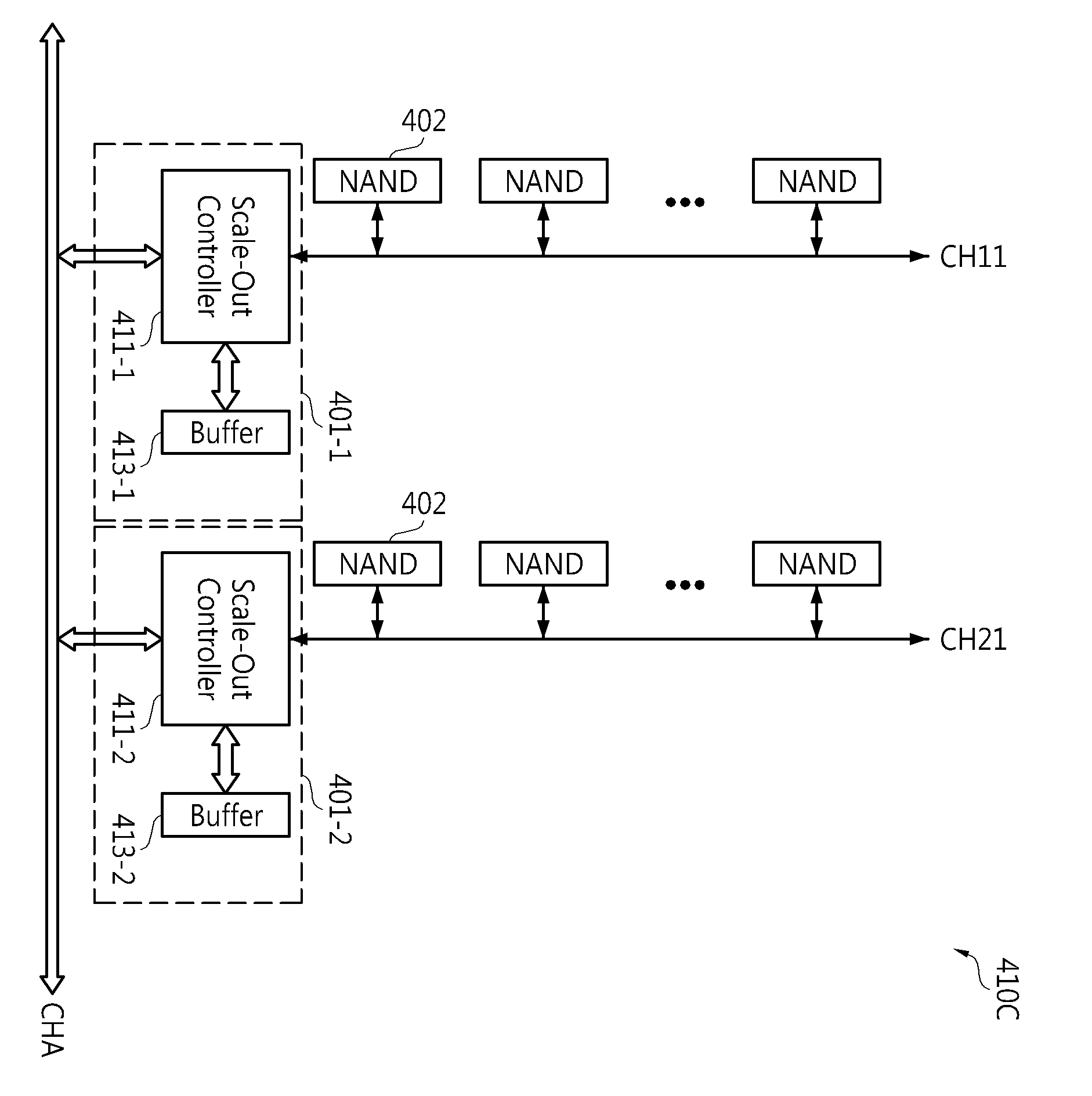
도 2는 도 1에 도시된 데이터 저장 장치의 상세 블록도이다. 도 2를 참조하면, 메모리 클러스터(400)는 복수의 스케일-아웃 장치들(401)과 복수의 불휘발성 메모리 장치들(402) 또는 복수의 불휘발성 메모리 패키지들(402)을 포함할 수 있다. 스케일-아웃 장치(401)는 하나의 채널 또는 하나의 웨이에 접속될 수 있다.FIG. 2 is a detailed block diagram of the data storage device shown in FIG. 1 . Referring to FIG. 2 , a
예컨대, 컨트롤러(310)가 A-채널*B-웨이를 지원할 때, 스케일-아웃 장치들 (401)의 개수는 A*B개일 수 있으나 이에 한정되는 것은 아니다. 여기서, A와 B 각각은 2 이상의 자연수이다. 예컨대, A와 B 각각이 8일 때, 메모리 클러스터(400)에 포함되는 스케일-아웃 장치들(401)의 개수는 64개일 수 있다.For example, when the
스케일-아웃 장치(401)는 C-채널*D-웨이로 확장 가능한 구조를 가지며, C*D 배로 확장된 불휘발성 메모리 장치들에 대한 논리 어드레스-물리 어드레스 매핑 정보를 저장하기 위한 고속-휘발성 메모리 인터페이스 기능을 지원할 수 있다. 예컨대, 스케일-아웃 장치(401)는 고속-휘발성 메모리 인터페이스 기능을 지원하기 위해 버퍼(예컨대, DRAM)를 포함할 수 있다. 여기서, C와 D 각각은 2 이상의 자연수이다.The scale-
도 3은 도 2에 도시된 스케일-아웃 장치의 블록도이다. 도 3을 참조하면, 스케일-아웃 장치(401)는 반도체 기판(401-3)의 위(on)에 부착된 스케일-아웃 컨트롤러(401-1)와 반도체 기판(401-3)의 위(on)에 부착된 하나 또는 그 이상의 버퍼들 (401-2)을 포함할 수 있다. 예컨대, 스케일-아웃 장치(401)는 멀티-칩 패키지 (multi-chip package(MCP))로 구현될 수 있으나 스케일-아웃 장치(401)의 구조가 이에 한정되는 것은 아니다. 예컨대, 버퍼는 DRAM으로 구현될 수 있다. 복수의 DRAM들은 스택 구조로 형성될 수 있다. 이때, 상기 복수의 DRAM들 각각은 본딩 와이어들을 통해 스케일-아웃 컨트롤러(401-1)와 통신할 수 있다.3 is a block diagram of the scale-out device shown in FIG. 2; Referring to FIG. 3, a scale-
도 4는 도 1에 도시된 제1클러스터의 일 실시 예를 나타내는 블록도이다. 도 1부터 도 4를 참조하면, 각 클러스터(410, 430, ..., 450)의 구조와 작동은 실질적으로 동일 또는 유사하므로, 제1클러스터(410A)의 구조와 작동이 대표적으로 설명된다.FIG. 4 is a block diagram illustrating an embodiment of the first cluster shown in FIG. 1 . Referring to FIGS. 1 through 4 , since the structure and operation of each
제1클러스터(410A)는 제1메인 채널(CHA)과 복수의 불휘발성 메모리 장치들 (NAND) 사이에 접속된 스케일-아웃 장치(401)를 포함할 수 있다. 스케일-아웃 장치 (401)는 스케일-아웃 컨트롤러(411-1)와 휘발성 메모리(413-1)를 포함할 수 있다.The
스케일-아웃 컨트롤러(411-1)는 제1메인 채널(CHA), 채널(CH11), 및 휘발성 메모리(413-1)에 접속될 수 있다. 스케일-아웃 컨트롤러(411-1)는 휘발성 메모리 (413-1)의 작동을 제어할 수 있고, 채널(CH11)에 접속된 불휘발성 메모리 장치들, 예컨대, NAND-타입 플래시 메모리들(NAND) 각각의 작동을 제어할 수 있다.The scale-out controller 411-1 may be connected to the first main channel CHA, the channel CH11, and the volatile memory 413-1. The scale-out controller 411-1 may control the operation of the volatile memory 413-1, and each of nonvolatile memory devices such as NAND-type flash memories (NAND) connected to the channel CH11 operation can be controlled.
불휘발성 메모리 장치들 각각은 PRAM 장치, MRAM 장치, STT-MRAM 장치, FRAM 장치, 또는 RRAM 장치로 구현될 수 있으나, 본 명세서에서는 설명의 편의를 위해 불휘발성 메모리 장치들의 실시 예로서 NAND-타입 플래시 메모리들을 예시적으로 도시하고 설명한다.Each of the nonvolatile memory devices may be implemented as a PRAM device, an MRAM device, an STT-MRAM device, a FRAM device, or an RRAM device, but in this specification, NAND-type flash is used as an embodiment of nonvolatile memory devices for convenience of description. Memories are shown and described by way of example.
NAND-타입 플래시 메모리(NAND)는 다이(die), 칩 다이(chip die), 칩 또는 패키지를 의미할 수 있다. NAND-타입 플래시 메모리(NAND)는 복수의 메모리 셀들을 포함하는 메모리 셀 어레이와, 상기 메모리 셀 어레이에 대한 데이터 처리 작동(예컨대, 프로그램 작동, 리드 작동, 또는 이레이즈 작동)을 제어할 수 있는 액세스 컨트롤(access control) 회로를 포함할 수 있다.A NAND-type flash memory (NAND) may refer to a die, a chip die, a chip, or a package. A NAND-type flash memory (NAND) includes a memory cell array including a plurality of memory cells and access capable of controlling a data processing operation (eg, a program operation, a read operation, or an erase operation) for the memory cell array. It may include access control circuitry.
상기 복수의 메모리 셀들 각각은 1-비트에 해당하는 정보를 저장할 수 있는 싱글-레벨 셀(single-level cell(SLC)) 또는 2-비트 이상에 해당하는 정보를 저장할 수 있는 멀티-레벨 셀(multi-level cell(MLC))을 의미할 수 있다.Each of the plurality of memory cells is a single-level cell (SLC) capable of storing information corresponding to 1-bit or a multi-level cell (multi-level cell) capable of storing information corresponding to 2-bits or more. -level cell (MLC)).
실시 예에 따라, 상기 메모리 셀 어레이는 2차원적으로 배열된 NAND-타입 플래시 메모리 셀들을 포함할 수 있다. 실시 예에 따라, 상기 메모리 셀 어레이는 3차원적인 수직(three-dimensional Vertical) NAND-타입 플래시 메모리 셀들을 포함할 수 있다.According to an embodiment, the memory cell array may include two-dimensionally arranged NAND-type flash memory cells. According to an embodiment, the memory cell array may include three-dimensional vertical NAND-type flash memory cells.
채널(CH11)은 스케일-아웃 컨트롤러(411-1)와 NAND-타입 플래시 메모리들 (NAND) 사이에 존재하는 독립적인 데이터 패스를 의미할 수 있다. 상기 데이터 패스는 데이터 및/또는 제어 신호들을 전송할 수 있는 전송 라인들을 포함할 수 있다. 웨이(way)는 채널(CH11)을 공유하는 하나 또는 그 이상의 NAND-타입 플래시 메모리들의 그룹을 의미할 수 있다. 따라서, 하나의 채널(CH11)에는 복수의 웨이들이 접속될 수 있다.Channel CH11 may mean an independent data path existing between the scale-out controller 411-1 and NAND-type flash memories (NAND). The data path may include transmission lines capable of transmitting data and/or control signals. A way may refer to a group of one or more NAND-type flash memories sharing the channel CH11. Accordingly, a plurality of ways may be connected to one channel CH11.
실시 예들에 따라, 스케일-아웃 컨트롤러(411-1)는, 컨트롤러(310)의 제어에 따라 또는 독립적으로, NAND-타입 플래시 메모리들(NAND) 각각에 대한 데이터 처리 작동 및/또는 휘발성 메모리(413-1)에 대한 데이터 처리 작동을 제어할 수 있다.According to embodiments, the scale-out controller 411-1 performs data processing operations and/or
휘발성 메모리(413-1)는 버퍼 또는 버퍼 메모리를 의미할 수 있고, RAM, SRAM, 또는 DRAM으로 구현될 수 있으나 휘발성 메모리(413-1)가 이에 한정되는 것은 아니다.The volatile memory 413-1 may mean a buffer or buffer memory, and may be implemented as RAM, SRAM, or DRAM, but the volatile memory 413-1 is not limited thereto.
실시 예에 따라, 휘발성 메모리(413-1)는 채널(CH11)에 접속된 NAND-타입 플래시 메모리들(NAND)에 대한 논리 어드레스-물리 어드레스 매핑 정보(또는 매핑 테이블)를 저장할 수 있는 제1메모리 영역을 포함할 수 있다. 또한, 휘발성 메모리 (413-1)는 채널(CH11)에 접속된 NAND-타입 플래시 메모리들(NAND) 중에서 적어도 하나에 라이트될 데이터 또는 NAND-타입 플래시 메모리들(NAND) 중에서 적어도 하나로부터 출력된 데이터를 임시로 저장할 수 있는 제2메모리 영역(또는 캐시 영역)을 더 포함할 수 있다.According to an embodiment, the volatile memory 413-1 is a first memory capable of storing logical address-physical address mapping information (or a mapping table) for the NAND-type flash memories NAND connected to the channel CH11. area can be included. In addition, the volatile memory 413-1 stores data to be written in at least one of the NAND-type flash memories (NAND) connected to the channel (CH11) or data output from at least one of the NAND-type flash memories (NAND). It may further include a second memory area (or cache area) capable of temporarily storing .
도 5는 도 1에 도시된 제1클러스터의 다른 실시 예를 나타내는 블록도이다.FIG. 5 is a block diagram illustrating another embodiment of the first cluster shown in FIG. 1 .
도 1부터 도 3, 및 도 5를 참조하면, 각 클러스터(410, 430, ..., 450)의 구조와 작동은 실질적으로 동일 또는 유사하므로, 제1클러스터(410B)의 구조와 작동이 대표적으로 설명된다.Referring to FIGS. 1 through 3 and 5, since the structure and operation of each
제1클러스터(410B)는 제1메인 채널(CHA)과 복수의 불휘발성 메모리 장치들 (NAND) 사이에 접속된 스케일-아웃 장치(401)를 포함할 수 있다. 스케일-아웃 장치 (401)는 스케일-아웃 컨트롤러(411-1)와 휘발성 메모리(413-1)를 포함할 수 있다.The
스케일-아웃 컨트롤러(411-1)는 제1메인 채널(CHA), 채널들(CH11~CH1m), 및 휘발성 메모리(413-1)에 접속될 수 있다. 스케일-아웃 컨트롤러(411-1)는 휘발성 메모리(413-1)의 작동을 제어할 수 있고, 각 채널(CH11~CH1m)에 접속된 불휘발성 메모리 장치들, 예컨대, NAND-타입 플래시 메모리들(NAND) 각각의 작동을 제어할 수 있다.The scale-out controller 411-1 may be connected to a first main channel CHA, channels CH11 to CH1m, and a volatile memory 413-1. The scale-out controller 411-1 can control the operation of the volatile memory 413-1, and non-volatile memory devices connected to each channel CH11 to CH1m, for example, NAND-type flash memories ( NAND) can control each operation.
제1그룹의 NAND-타입 플래시 메모리들(NAND)은 채널(CH11)에 접속될 수 있고, 제m그룹의 NAND-타입 플래시 메모리들(NAND)은 채널(CH1m)에 접속될 수 있다. 예컨대, 복수의 웨이들은 채널(CH11)에 접속될 수 있고, 복수의 웨이들은 채널 (CH1m)에 접속될 수 있다.The first group of NAND-type flash memories NAND may be connected to the channel CH11, and the mth group of NAND-type flash memories NAND may be connected to the channel CH1m. For example, a plurality of ways may be connected to a channel CH11, and a plurality of ways may be connected to a channel CH1m.
스케일-아웃 컨트롤러(411-1)는, 컨트롤러(310)의 제어에 따라 또는 독립적으로, 각 채널(CH11~CH1m)에 접속된 NAND-타입 플래시 메모리들(NAND) 각각에 대한 데이터 처리 작동 및/또는 휘발성 메모리(413-1)에 대한 데이터 처리 작동을 제어할 수 있다.The scale-out controller 411-1 performs data processing for each of the NAND-type flash memories (NAND) connected to each channel (CH11 to CH1m) under the control of the
실시 예에 따라, 휘발성 메모리(413-1)는 각 채널(CH11~CH1m)에 접속된 NAND-타입 플래시 메모리들(NAND)에 대한 논리 어드레스-물리 어드레스 매핑 정보(또는 매핑 테이블)를 저장할 수 있는 제1메모리 영역을 포함할 수 있다. 또한, 휘발성 메모리(413-1)는 각 채널(CH11~CH1m)에 접속된 NAND-타입 플래시 메모리들 (NAND) 중에서 적어도 하나에 라이트될 데이터 또는 각 채널(CH11~CH1m)에 접속된 NAND-타입 플래시 메모리들(NAND) 중에서 적어도 하나로부터 출력된 데이터를 임시로 저장할 수 있는 제2메모리 영역(또는 캐시 영역)을 더 포함할 수 있다.According to an embodiment, the volatile memory 413-1 may store logical address-physical address mapping information (or a mapping table) for NAND-type flash memories (NAND) connected to each channel (CH11 to CH1m). It may include a first memory area. In addition, the volatile memory 413-1 includes data to be written in at least one of the NAND-type flash memories (NAND) connected to each channel (CH11 to CH1m) or a NAND-type connected to each channel (CH11 to CH1m). A second memory area (or cache area) capable of temporarily storing data output from at least one of the flash memories NAND may be further included.
도 6은 도 1에 도시된 제1클러스터의 또 다른 실시 예를 나타내는 블록도이다. 도 1부터 도 3, 및 도 6을 참조하면, 각 클러스터(410, 430, ..., 450)의 구조와 작동은 실질적으로 동일 또는 유사하므로, 제1클러스터(410C)의 구조와 작동이 대표적으로 설명된다.FIG. 6 is a block diagram illustrating another embodiment of the first cluster shown in FIG. 1 . 1 through 3 and 6, since the structure and operation of each
제1클러스터(410C)는 스케일-아웃 장치들(401-1과 401-2)과 복수의 불휘발성 메모리 장치들(NAND)을 포함할 수 있다. The
제1클러스터(410C)는 제1메인 채널(CHA)과 채널(CH11) 사이에 접속된 제1스케일-아웃 컨트롤러(411-1), 제1스케일-아웃 컨트롤러(411-1)에 접속된 제1휘발성 메모리(413-1), 채널(CH11)에 접속된 NAND-타입 플래시 메모리들(NAND), 제1메인 채널(CHA)과 채널(CH21) 사이에 접속된 제2스케일-아웃 컨트롤러(411-2), 제2스케일-아웃 컨트롤러(411-2)에 접속된 제2휘발성 메모리(413-2), 채널(CH21)에 접속된 NAND-타입 플래시 메모리들(NAND)을 포함할 수 있다.The
해당하는 NAND-타입 플래시 메모리들(NAND)은 채널(CH11)에 접속되고, 해당하는 NAND-타입 플래시 메모리들(NAND)은 채널(CH21)에 접속된다. 예컨대, 복수의 웨이들은 채널(CH11)에 접속될 수 있고, 복수의 웨이들은 채널(CH21)에 접속될 수 있다.Corresponding NAND-type flash memories NAND are connected to channel CH11, and corresponding NAND-type flash memories NAND are connected to channel CH21. For example, a plurality of ways may be connected to the channel CH11, and a plurality of ways may be connected to the channel CH21.
제1스케일-아웃 컨트롤러(411-1)는, 컨트롤러(310)의 제어에 따라 또는 독립적으로, 채널(CH11)에 접속된 NAND-타입 플래시 메모리들(NAND) 각각에 대한 데이터 처리 작동 및/또는 제1휘발성 메모리(413-1)에 대한 데이터 처리 작동을 제어할 수 있다.The first scale-out controller 411-1 performs data processing for each of the NAND-type flash memories NAND connected to the channel CH11 under the control of the
실시 예에 따라, 제1휘발성 메모리(413-1)는 채널(CH11)에 접속된 NAND-타입 플래시 메모리들(NAND)에 대한 논리 어드레스-물리 어드레스 매핑 정보(또는 매핑 테이블)를 저장할 수 있는 제1메모리 영역을 포함할 수 있다. 또한, 제1휘발성 메모리(413-1)는 채널(CH11)에 접속된 NAND-타입 플래시 메모리들(NAND) 중에서 적어도 하나에 라이트될 데이터 또는 NAND-타입 플래시 메모리들(NAND) 중에서 적어도 하나로부터 출력된 데이터를 임시로 저장할 수 있는 제2메모리 영역(또는 캐시 영역)을 더 포함할 수 있다.According to an embodiment, the first volatile memory 413-1 may store logical address-physical address mapping information (or a mapping table) for the NAND-type flash memories NAND connected to the channel CH11. It can contain 1 memory area. In addition, the first volatile memory 413-1 includes data to be written to at least one of the NAND-type flash memories (NAND) connected to the channel (CH11) or output from at least one of the NAND-type flash memories (NAND). It may further include a second memory area (or cache area) capable of temporarily storing stored data.
제2스케일-아웃 컨트롤러(411-2)는, 컨트롤러(310)의 제어에 따라 또는 독립적으로, 채널(CH21)에 접속된 NAND-타입 플래시 메모리들(NAND) 각각에 대한 데이터 처리 작동 및/또는 제2휘발성 메모리(413-2)에 대한 데이터 처리 작동을 제어할 수 있다.The second scale-out controller 411-2 performs data processing for each of the NAND-type flash memories NAND connected to the channel CH21 under the control of the
실시 예에 따라, 제2휘발성 메모리(413-2)는 채널(CH21)에 접속된 NAND-타입 플래시 메모리들(NAND)에 대한 논리 어드레스-물리 어드레스 매핑 정보(또는 매핑 테이블)를 저장할 수 있는 제1메모리 영역을 포함할 수 있다. 또한, 제2휘발성 메모리(413-2)는 채널(CH21)에 접속된 NAND-타입 플래시 메모리들(NAND) 중에서 적어도 하나에 라이트될 데이터 또는 NAND-타입 플래시 메모리들(NAND) 중에서 적어도 하나로부터 출력된 데이터를 임시로 저장할 수 있는 제2메모리 영역(또는 캐시 영역)을 더 포함할 수 있다.According to an embodiment, the second volatile memory 413-2 may store logical address-physical address mapping information (or a mapping table) for the NAND-type flash memories NAND connected to the channel CH21. It can contain 1 memory area. In addition, the second volatile memory 413-2 includes data to be written in at least one of the NAND-type flash memories (NAND) connected to the channel CH21 or output from at least one of the NAND-type flash memories (NAND). It may further include a second memory area (or cache area) capable of temporarily storing stored data.
도 7은 도 1에 도시된 제1클러스터의 또 다른 실시 예를 나타내는 블록도이다. 도 1부터 도 3, 및 도 5를 참조하면, 각 클러스터(410, 430, ..., 450)의 구조와 작동은 실질적으로 동일 또는 유사하므로, 제1클러스터(410D)의 구조와 작동이 대표적으로 설명된다.FIG. 7 is a block diagram illustrating another embodiment of the first cluster shown in FIG. 1 . Referring to FIGS. 1 through 3 and 5, since the structure and operation of each
제1클러스터(410D)는 스케일-아웃 장치들(401-1과 401-2)과 복수의 불휘발성 메모리 장치들(NAND)을 포함할 수 있다. 제1스케일-아웃 장치(401-1)는 제1스케일-아웃 컨트롤러(411-1)와 제1휘발성 메모리(413-1)를 포함하고, 제2스케일-아웃 장치(401-2)는 제2스케일-아웃 컨트롤러(411-2)와 제2휘발성 메모리(413-2)를 포함할 수 있다.The
제1스케일-아웃 컨트롤러(411-1)는 메인 채널(CHA), 채널들(CH11~CH1m), 및 제1휘발성 메모리(413-1)에 접속될 수 있다. 각 채널(CH11~CH1m)에는 대응되는 NAND-타입 플래시 메모리들(NAND)이 접속될 수 있다.The first scale-out controller 411-1 may be connected to the main channel CHA, the channels CH11 to CH1m, and the first volatile memory 413-1. Corresponding NAND-type flash memories NAND may be connected to each channel CH11 to CH1m.
제1휘발성 메모리(413-1)는 각 채널(CH11~CH1m)에 접속된 대응되는 NAND-타입 플래시 메모리들(NAND)에 대한 논리 어드레스-물리 어드레스 매핑 정보(또는 매핑 테이블)를 저장할 수 있는 제1메모리 영역을 포함할 수 있다. 또한, 제1휘발성 메모리(413-1)는 각 채널(CH11~CH1m)에 접속된 대응되는 NAND-타입 플래시 메모리들(NAND) 중에서 적어도 하나에 라이트될 데이터 또는 각 채널(CH11~CH1m)에 접속된 대응되는 NAND-타입 플래시 메모리들(NAND) 중에서 적어도 하나로부터 출력된 데이터를 임시로 저장할 수 있는 제2메모리 영역(또는 캐시 영역)을 더 포함할 수 있다.The first volatile memory 413-1 may store logical address-physical address mapping information (or a mapping table) for corresponding NAND-type flash memories NAND connected to each channel CH11 to CH1m. It can contain 1 memory area. In addition, the first volatile memory 413-1 is connected to data to be written in at least one of the corresponding NAND-type flash memories NAND connected to each channel CH11 to CH1m or to each channel CH11 to CH1m. A second memory area (or cache area) capable of temporarily storing data output from at least one of the corresponding NAND-type flash memories (NAND) may be further included.
제2스케일-아웃 컨트롤러(411-2)는 메인 채널(CHA), 채널들(CH21~CH2m), 및 제2휘발성 메모리(413-2)에 접속될 수 있다. 각 채널(CH21~CH2m)에는 대응되는 NAND-타입 플래시 메모리들(NAND)이 접속될 수 있다.The second scale-out controller 411-2 may be connected to the main channel CHA, the channels CH21 to CH2m, and the second volatile memory 413-2. Corresponding NAND-type flash memories NAND may be connected to each channel CH21 to CH2m.
제2휘발성 메모리(413-2)는 각 채널(CH21~CH2m)에 접속된 대응되는 NAND-타입 플래시 메모리들(NAND)에 대한 논리 어드레스-물리 어드레스 매핑 정보(또는 매핑 테이블)를 저장할 수 있는 제1메모리 영역을 포함할 수 있다. 또한, 제3휘발성 메모리(413-2)는 각 채널(CH21~CH2m)에 접속된 대응되는 NAND-타입 플래시 메모리들(NAND) 중에서 적어도 하나에 라이트될 데이터 또는 각 채널(CH21~CH2m)에 접속된 대응되는 NAND-타입 플래시 메모리들(NAND) 중에서 적어도 하나로부터 출력된 데이터를 임시로 저장할 수 있는 제2메모리 영역(또는 캐시 영역)을 더 포함할 수 있다.The second volatile memory 413-2 may store logical address-physical address mapping information (or a mapping table) for corresponding NAND-type flash memories NAND connected to each channel CH21 to CH2m. It can contain 1 memory area. In addition, the third volatile memory 413-2 is connected to data to be written in at least one of the corresponding NAND-type flash memories NAND connected to each channel CH21 to CH2m or to each channel CH21 to CH2m. A second memory area (or cache area) capable of temporarily storing data output from at least one of the corresponding NAND-type flash memories (NAND) may be further included.
도 8은 도 1에 도시된 제1클러스터의 또 다른 실시 예를 나타내는 블록도이다. 도 1부터 도 3, 및 도 8을 참조하면, 각 클러스터(410, 430, ..., 450)의 구조와 작동은 실질적으로 동일 또는 유사하므로, 제1클러스터(410E)의 구조와 작동이 대표적으로 설명된다.FIG. 8 is a block diagram illustrating another embodiment of the first cluster shown in FIG. 1 . 1 to 3 and 8, since the structure and operation of each
제1클러스터(410E)는 스케일-아웃 장치들(401-1~401-k)과 복수의 불휘발성 메모리 장치들(NAND)을 포함할 수 있다.The
제1스케일-아웃 컨트롤러(411-1)는 메인 채널(CHA), 채널들(CH11~CH1m), 및 제1휘발성 메모리(413-1)에 접속될 수 있다. 각 채널(CH11~CH1m)에는 대응되는 NAND-타입 플래시 메모리들(NAND)이 접속될 수 있다.The first scale-out controller 411-1 may be connected to the main channel CHA, the channels CH11 to CH1m, and the first volatile memory 413-1. Corresponding NAND-type flash memories NAND may be connected to each channel CH11 to CH1m.
제1휘발성 메모리(413-1)는 각 채널(CH11~CH1m)에 접속된 대응되는 NAND-타입 플래시 메모리들(NAND)에 대한 논리 어드레스-물리 어드레스 매핑 정보(또는 매핑 테이블)를 저장할 수 있는 제1메모리 영역을 포함할 수 있다. 또한, 제1휘발성 메모리(413-1)는 각 채널(CH11~CH1m)에 접속된 대응되는 NAND-타입 플래시 메모리들(NAND) 중에서 적어도 하나에 라이트될 데이터 또는 각 채널(CH11~CH1m)에 접속된 대응되는 NAND-타입 플래시 메모리들(NAND) 중에서 적어도 하나로부터 출력된 데이터를 임시로 저장할 수 있는 제2메모리 영역(또는 캐시 영역)을 더 포함할 수 있다.The first volatile memory 413-1 may store logical address-physical address mapping information (or a mapping table) for corresponding NAND-type flash memories NAND connected to each channel CH11 to CH1m. It can contain 1 memory area. In addition, the first volatile memory 413-1 is connected to data to be written in at least one of the corresponding NAND-type flash memories NAND connected to each channel CH11 to CH1m or to each channel CH11 to CH1m. A second memory area (or cache area) capable of temporarily storing data output from at least one of the corresponding NAND-type flash memories (NAND) may be further included.
제2스케일-아웃 컨트롤러(411-2)는 메인 채널(CHA), 채널들(CH21~CH2m), 및 제2휘발성 메모리(413-2)에 접속될 수 있다. 각 채널(CH21~CH2m)에는 대응되는 NAND-타입 플래시 메모리들(NAND)이 접속될 수 있다.The second scale-out controller 411-2 may be connected to the main channel CHA, the channels CH21 to CH2m, and the second volatile memory 413-2. Corresponding NAND-type flash memories NAND may be connected to each channel CH21 to CH2m.
제2휘발성 메모리(413-2)는 각 채널(CH21~CH2m)에 접속된 대응되는 NAND-타입 플래시 메모리들(NAND)에 대한 논리 어드레스-물리 어드레스 매핑 정보(또는 매핑 테이블)를 저장할 수 있는 제1메모리 영역을 포함할 수 있다. 또한, 제2휘발성 메모리(413-2)는 각 채널(CH21~CH2m)에 접속된 대응되는 NAND-타입 플래시 메모리들(NAND) 중에서 적어도 하나에 라이트될 데이터 또는 각 채널(CH21~CH2m)에 접속된 대응되는 NAND-타입 플래시 메모리들(NAND) 중에서 적어도 하나로부터 출력된 데이터를 임시로 저장할 수 있는 제2메모리 영역(또는 캐시 영역)을 더 포함할 수 있다.The second volatile memory 413-2 may store logical address-physical address mapping information (or a mapping table) for corresponding NAND-type flash memories NAND connected to each channel CH21 to CH2m. It can contain 1 memory area. In addition, the second volatile memory 413-2 is connected to data to be written in at least one of the corresponding NAND-type flash memories (NAND) connected to each channel (CH21 to CH2m) or to each channel (CH21 to CH2m). A second memory area (or cache area) capable of temporarily storing data output from at least one of the corresponding NAND-type flash memories (NAND) may be further included.
제k스케일-아웃 컨트롤러(411-k)는 메인 채널(CHA), 채널들(CHk1~CHkm), 및 제k휘발성 메모리(413-k)에 접속될 수 있다. 각 채널(CHk1~CHkm)에는 대응되는 NAND-타입 플래시 메모리들(NAND)이 접속될 수 있다.The kth scale-out controller 411-k may be connected to the main channel CHA, the channels CHk1 to CHkm, and the kth volatile memory 413-k. Corresponding NAND-type flash memories NAND may be connected to each channel CHk1 to CHkm.
제k휘발성 메모리(413-2)는 각 채널(CHk1~CHkm)에 접속된 대응되는 NAND-타입 플래시 메모리들(NAND)에 대한 논리 어드레스-물리 어드레스 매핑 정보(또는 매핑 테이블)를 저장할 수 있는 제1메모리 영역을 포함할 수 있다. 또한, 제k휘발성 메모리(413-k)는 각 채널(CHk1~CHkm)에 접속된 대응되는 NAND-타입 플래시 메모리들(NAND) 중에서 적어도 하나에 라이트될 데이터 또는 각 채널(CHk1~CHkm)에 접속된 대응되는 NAND-타입 플래시 메모리들(NAND) 중에서 적어도 하나로부터 출력된 데이터를 임시로 저장할 수 있는 제2메모리 영역(또는 캐시 영역)을 더 포함할 수 있다.The k-th volatile memory 413-2 may store logical address-physical address mapping information (or a mapping table) for corresponding NAND-type flash memories NAND connected to each channel CHk1 to CHkm. It can contain 1 memory area. In addition, the kth volatile memory 413-k is connected to data to be written in at least one of the corresponding NAND-type flash memories NAND connected to each channel CHk1 to CHkm or to each channel CHk1 to CHkm. A second memory area (or cache area) capable of temporarily storing data output from at least one of the corresponding NAND-type flash memories (NAND) may be further included.
메인 채널(CHA)에 접속될 수 있는 클러스터(410)는 도 4부터 도 8을 참조하며 설명한 클러스터들(410A~410E) 중에서 어느 하나로 구현될 수 있고, 메인 채널 (CHB)에 접속될 수 있는 클러스터(430)는 도 4부터 도 8을 참조하며 설명한 클러스터들(410A~410E) 중에서 어느 하나로 구현될 수 있고, 메인 채널(CHC)에 접속될 수 있는 클러스터(450)는 도 4부터 도 8을 참조하며 설명한 클러스터들(410A~410E) 중에서 어느 하나로 구현될 수 있다.The
각 휘발성 메모리(413-1~413-k)는 버퍼 또는 버퍼 메모리를 의미할 수 있고, RAM, SRAM, 또는 DRAM으로 구현될 수 있으나 이에 한정되는 것은 아니다.Each of the volatile memories 413-1 to 413-k may mean a buffer or buffer memory, and may be implemented as RAM, SRAM, or DRAM, but is not limited thereto.
도 9는 도 2부터 도 8에 도시된 스케일-아웃 장치의 개략도이고, 도 10은 도 9에 도시된 스케일-아웃 컨트롤러의 블록도이다.9 is a schematic diagram of the scale-out device shown in FIGS. 2 to 8 , and FIG. 10 is a block diagram of the scale-out controller shown in FIG. 9 .
도 1부터 도 10을 참조하면, 각 스케일-아웃 컨트롤러(411-1~411-k)의 구조와 작동은 실질적으로 동일 또는 유사하므로, 제1스케일-아웃 컨트롤러(411-1)의 구조와 작동이 대표적으로 설명될 것이다.1 to 10, since the structure and operation of each scale-out controller 411-1 to 411-k are substantially the same or similar, the structure and operation of the first scale-out controller 411-1 This will be explained representatively.
제1스케일-아웃 컨트롤러(411-1)는 컨트롤러(310), 제1휘발성 메모리(413-1), 및 NAND-타입 플래시 메모리들(NAND) 사이에서 주거나 받는 명령 및/또는 데이터를 제어할 수 있다. 실시 예들에 따라, 제1스케일-아웃 컨트롤러(411-1)는 칩, IC 또는 SoC로 구현될 수 있다. 제1휘발성 메모리(413-1)가 DRAM으로 구현될 때, 제1스케일-아웃 컨트롤러(411-1)는 DRAM 인터페이스를 포함할 수 있다.The first scale-out controller 411-1 may control commands and/or data sent or received between the
제1스케일-아웃 컨트롤러(411-1)는 하나의 채널 또는 하나의 웨이에 접속되는 입력 단자(또는 입력 포트), 복수의 채널들 또는 복수의 웨이들에 접속될 수 있는 출력 단자들(또는 출력 포트들), 및 제1휘발성 메모리(413-1)에 접속될 수 있는 인터페이스를 포함할 수 있다.The first scale-out controller 411-1 includes an input terminal (or input port) connected to one channel or one way, and output terminals (or output terminals) that can be connected to a plurality of channels or a plurality of ways. ports), and an interface that can be connected to the first volatile memory 413-1.
제1스케일-아웃 컨트롤러(411-1)는 버스 구조(또는 버스; 420), 제4인터페이스(421), 적어도 하나의 CPU(423-1 및/또는 423-2), 내부 메모리(425), 버퍼 컨트롤러(427), 및 제5인터페이스(429)를 포함할 수 있다.The first scale-out controller 411-1 includes a bus structure (or bus) 420, a
버스 구조(420)는 AMBA, AHB, APB, AXI, ASB, 또는 이들의 결합으로 구현될 수 있으나 이에 한정되는 것은 아니다.The
제4인터페이스(421)는 컨트롤러(310)로 전송될 응답 및/또는 데이터의 포맷을 변경하고, 변경된 응답 및/또는 변경된 데이터를 메인 채널(CHA)을 통해 컨트롤러(310)로 전송할 수 있다. 또한, 제4인터페이스(421)는 컨트롤러(310)로부터 전송된 명령 및/또는 데이터를 수신하고, 수신된 명령 및/또는 데이터의 포맷을 변경하고, 변경된 명령 및/또는 변경된 데이터를 적어도 하나의 CPU(423-1 및/또는 423-2) 및/또는 버퍼 컨트롤러(427)로 전송할 수 있다. 실시 예에 따라, 제4인터페이스(421)는 신호 및/또는 데이터를 송수신할 수 있는 송수신기를 포함할 수 있다.The
제4인터페이스(421)의 구조와 작동은 제3인터페이스(350)의 구조와 작동에 적합하게 구현될 수 있다. 예컨대, 제4인터페이스(421)는 SATA 인터페이스, SATAe 인터페이스, SAS, PCIe 인터페이스, NVMe 인터페이스, AHCI, NAND-타입 플래시 메모리 인터페이스, 또는 NOR-타입 플래시 메모리 인터페이스로 구현될 수 있으나 이에 한정되는 것은 아니다. 실시 예에 따라, 제4인터페이스(421)는 하나의 채널 또는 하나의 웨이에 접속될 수 있다.The structure and operation of the
하나 또는 그 이상의 CPU(423-1 및/또는 423-3)는, 버스 구조(420)를 통해, 제4인터페이스(421), 내부 메모리(425), 버퍼 컨트롤러(427), 및 제5인터페이스 (429)를 제어할 수 있다. 각 CPU(423-1 및/또는 423-3)는 하나 또는 그 이상의 코어들을 포함할 수 있다.One or more CPUs 423-1 and/or 423-3 connect a
예컨대, 제1CPU(423-1)는 제4인터페이스(421)를 통해 제3인터페이스(350)와의 상호 작동을 제어할 수 있고, 제2CPU(423-2)는 제5인터페이스(429)를 통해 각 채널(CH11~CH1m)에 접속된 NAND-타입 플래시 메모리들(NAND)과의 상호 작동을 제어할 수 있다. 실시 예에 따라, 제1CPU(423-1)와 제2CPU(423-2)는 멀티-CPU를 구성할 수 있다. 실시 예에 따라, 제1CPU(423-1)는 제2CPU(423-2)를 제어할 수 있다.For example, the first CPU 423-1 may control mutual operation with the
내부 메모리(425)는 제1스케일-아웃 컨트롤러(411-1)의 작동에 필요한 데이터 또는 제1스케일-아웃 컨트롤러(411-1)에 의해 수행된 데이터 처리 작동(예컨대, 라이트 작동 또는 리드 작동)에 의해 생성된 데이터를 저장할 수 있다. 내부 메모리(425)는 CPU(423-1 및/또는 423-2)에 의해 실행될 수 있는 제2FTL 코드(FTL2)를 저장할 수 있다. 실시 예들에 따라, 내부 메모리(425)는 RAM, DRAM, SRAM, 버퍼, 버퍼 메모리, 캐시, 또는 TCM으로 구현될 수 있으나 이에 한정되는 것은 아니다.The
버퍼 컨트롤러(427)는, 제1CPU(423-1) 또는 제2CPU(423-2)의 제어에 따라, 제1휘발성 메모리(413-1)에 데이터를 라이트하거나 제1휘발성 메모리(413-1)에 저장된 데이터를 리드할 수 있다. 버퍼 컨트롤러(427)는 제1휘발성 메모리(413-1)에 대한 라이트 작동과 리드 작동을 제어할 수 있는 컨트롤러 또는 버퍼 매니저로 불릴 수 있다.The
스케일-아웃 컨트롤러(411-1)는 버퍼 컨트롤러(427)에 의해 제어되는 내부 버퍼(427-1)를 더 포함할 수 있다. 비록, 도 10에서는 내부 버퍼(427-1)가 버퍼 컨트롤러(427)의 내부에 구현된 실시 예가 도시되어 있으나 내부 버퍼(427-1)는 스케일-아웃 컨트롤러(411-1) 내부에 구현될 수 있다. 예컨대, 내부 버퍼(427-1)는 SRAM으로 구현될 수 있다. 제1휘발성 메모리(413-1)는 외부 버퍼의 기능을 수행할 수 있고 DRAM으로 구현될 수 있다.The scale-out controller 411-1 may further include an internal buffer 427-1 controlled by the
제5인터페이스(429)는, 제1CPU(423-1) 또는 제2CPU(423-2)의 제어에 따라, 복수의 채널들(CH11~CH1m) 중에서 해당하는 채널을 통해 NAND-타입 플래시 메모리들(NAND)에 대한 데이터 처리 작동들을 제어할 수 있다.The
도 4부터 도 8을 참조하여 설명한 바와 같이, 복수의 채널들 및/또는 복수의 웨이들은 제5인터페이스(429)에 접속될 수 있다.As described with reference to FIGS. 4 through 8 , a plurality of channels and/or a plurality of ways may be connected to the
실시 예들에 따라 제5인터페이스(429)는 SATA 인터페이스, SATAe 인터페이스, SAS, PCIe 인터페이스, NVMe 인터페이스, AHCI, NAND-타입 플래시 메모리 인터페이스, 또는 NOR-타입 플래시 메모리 인터페이스로 구현될 수 있으나 제5인터페이스(429)가 이에 한정되는 것은 아니다.According to embodiments, the
ECC 엔진(429-1)은 불휘발성 메모리 장치들(NAND)에 저장될 데이터 및/또는 불휘발성 메모리 장치들(NAND)로부터 출력된 데이터에 포함된 에러를 정정할 수 있다. 비록, 도 10에서는 ECC 엔진(429-1)이 제5인터페이스(429)의 내부에 구현된 실시 예가 도시되어 있으나 ECC 엔진(429-1)은 스케일-아웃 컨트롤러(411-1)의 내부에 구현될 수 있다.The ECC engine 429 - 1 may correct errors included in data to be stored in the nonvolatile memory devices NAND and/or data output from the nonvolatile memory devices NAND. Although FIG. 10 shows an embodiment in which the ECC engine 429-1 is implemented inside the
실시 예에 따라, 제1스케일-아웃 컨트롤러(411-1)와 제1휘발성 메모리(413-1) 각각이 서로 다른 반도체 칩으로 구현될 때, 제1스케일-아웃 컨트롤러(411-1)와 제1휘발성 메모리(413-1)는 하나의 패키지, 예컨대, PoP, MCP, 또는 SiP로 구현될 수 있으나 이에 한정되는 것은 아니다. 예컨대, 제1휘발성 메모리(413-1)를 포함하는 제1칩은 제1스케일-아웃 컨트롤러(411-1)를 포함하는 제2칩의 위(above)에 스택 볼들을 통해 적층될 수 있다.According to an embodiment, when the first scale-out controller 411-1 and the first volatile memory 413-1 are implemented as different semiconductor chips, the first scale-out controller 411-1 and the first scale-out controller 411-1 One volatile memory 413-1 may be implemented as one package, for example, PoP, MCP, or SiP, but is not limited thereto. For example, the first chip including the first volatile memory 413-1 may be stacked above the second chip including the first scale-out controller 411-1 through stack balls.
도 4부터 도 8에 도시된 NAND-타입 플래시 메모리(NAND)가 스케일-아웃 컨트롤러(411-1)와 휘발성 메모리(413-1)를 포함하는 스케일-아웃 장치(401)로 대체되면, 메모리 클러스터(400)에 대한 용량의 확장성(scalability)은 증가할 수 있다.When the NAND-type flash memory (NAND) shown in FIGS. 4 to 8 is replaced with a scale-
도 11은 도 1에 도시된 제3인터페이스의 블록도이다.11 is a block diagram of a third interface shown in FIG. 1;
도 1과 도 11을 참조하면, 제3인터페이스(350)는 복수의 DMA(direct memory access) 컨트롤러들(351-1~351-n; n은 3 이상의 자연수), 복수의 ECC 엔진들(352-1~352-n), 및 복수의 NAND 컨트롤러들(353-1~353-n)을 포함할 수 있다.1 and 11, the
제1채널(Channel#1)은 제1메인 채널(CHA)에 대응되고, 제2채널(Channel#2)은 제2메인 채널(CHB)에 대응되고, 제n채널(Channel#n)은 제n메인 채널(CHC)에 대응된다고 가정한다.The first channel (Channel#1) corresponds to the first main channel (CHA), the second channel (Channel#2) corresponds to the second main channel (CHB), and the nth channel (Channel#n) corresponds to the It is assumed that n corresponds to the main channel (CHC).
제1채널(Channel#1)에 접속된 제1NAND 컨트롤러(353-1)는, 제1DMA 컨트롤러 (351-1)와 버퍼 컨트롤러(340)를 이용하여, 외부 버퍼(360)에 데이터를 라이트하거나 외부 버퍼(360)로부터 데이터를 리드할 수 있다. 제2채널(Channel#2)에 접속된 제2NAND 컨트롤러(353-2)는, 제2DMA 컨트롤러(351-2)와 버퍼 컨트롤러(340)를 이용하여, 외부 버퍼(360)에 데이터를 라이트하거나 외부 버퍼(360)로부터 데이터를 리드할 수 있다. 제n채널(Channel#n)에 접속된 제nNAND 컨트롤러(353-n)는, 제nDMA 컨트롤러(351-n)와 버퍼 컨트롤러(340)를 이용하여, 외부 버퍼(360)에 데이터를 라이트하거나 외부 버퍼(360)로부터 데이터를 리드할 수 있다.The first NAND controller 353-1 connected to the first channel (Channel#1) writes data to the
상술한 바와 같이, 제3인터페이스(350)는 SATA 인터페이스, SATAe 인터페이스, SAS, PCIe 인터페이스, NVMe 인터페이스, AHCI, NAND-타입 플래시 메모리 인터페이스, 또는 NOR-타입 플래시 메모리 인터페이스로 구현될 수 있으나, 도 11에서는 NAND-타입 플래시 메모리 인터페이스로 구현된 제3인터페이스(350)가 예시적으로 도시되어 있다.As described above, the
실시 예들에 따라, 도 10에 도시된 제5인터페이스(429)의 구조는 도 11에 도시된 제3인터페이스(350)의 구조와 실질적으로 동일 또는 유사하게 구현될 수 있다. 각 ECC 엔진(352-1~352-n)은 데이터에 대한 에러를 정정할 수 있다.According to embodiments, the structure of the
도 12는 본 발명의 실시 예에 따른 논리 어드레스-물리 어드레스 매핑 테이블들의 실시 예들이다.12 illustrates examples of logical address-physical address mapping tables according to an embodiment of the present invention.
도 1부터 도 12의 (a)를 참조하면, 외부 버퍼(360)는 제1테이블(TABLE1)을 저장할 수 있다. 즉, 제1FTL 코드(FTL1)는, 제1테이블(TABLE1)을 이용하여, 해당하는 논리 어드레스들을 해당하는 스케일-아웃 컨트롤러에 할당할 수 있다.Referring to (a) of FIG. 1 to FIG. 12 , the
예컨대, 논리 블록 어드레스들(logical block addresses; LBA0~LBA999)은 제1스케일-아웃 컨트롤러(Scale-Out Controller#1)에 할당될 수 있고, 논리 블록 어드레스들 (LBA1000~LBA1999)은 제2스케일-아웃 컨트롤러(Scale-Out Controller#2)에 할당될 수 있고, 논리 블록 어드레스들(LBA2000~LBA2999)은 제3스케일-아웃 컨트롤러 (Scale-Out Controller#3)에 할당될 수 있고, 논리 블록 어드레스들 (LBA3000~LBA3999)은 제4스케일-아웃 컨트롤러(Scale-Out Controller#4)에 할당될 수 있다.For example, logical block addresses (LBA0 to LBA999) may be assigned to a first scale-out controller (Scale-Out Controller#1), and logical block addresses (LBA1000 to LBA1999) may be assigned to a second scale-out controller (Scale-Out Controller#1). It can be allocated to the out controller (Scale-Out Controller#2), and the logical block addresses (LBA2000 to LBA2999) can be allocated to the third scale-out controller (Scale-Out Controller#3), and the logical block addresses (LBA3000 to LBA3999) may be assigned to the fourth scale-out controller (Scale-Out Controller#4).
각 스케일-아웃 컨트롤러(Scale-Out Controller#1~Scale-Out Controller#4)는 클러스터들(410, 430, ..., 450) 중에서 적어도 하나에 포함될 수 있다.Each of the scale-out controllers (Scale-
데이터 저장 장치(300)는 복수의 클러스터들(410~450)을 포함할 수 있고, 각 클러스터(410~450)는 각 스케일-아웃 컨트롤러와 각 휘발성 메모리를 포함할 수 있다.The
종래의 데이터 저장 장치는 컨트롤러(310)에 대응되는 하나의 레거시 (legacy) 컨트롤러와 외부 버퍼(360)에 대응되는 하나의 버퍼를 포함하고, 하나의 FTL는 상기 하나의 레거시 컨트롤러에 의해 관리되었다.A conventional data storage device includes one legacy controller corresponding to the
그러나, 데이터 저장 장치(300)는 하나의 컨트롤러(310) 이외에 복수의 클러스터들(410~450) 중에서 적어도 하나에 포함된 적어도 하나의 스케일-아웃 컨트롤러를 포함하므로, 하나의 FTL은 상기 적어도 하나의 스케일-아웃 컨트롤러에 분산되어 저장되고 실행될 수 있다.However, since the
즉, 스케일-아웃 컨트롤러들 각각은 분산된 FTL을 포함하고, 상기 분산된 FTL은 복수의 채널들 및/또는 복수의 웨이들에 접속된 불휘발성 메모리 장치들, 예컨대, NAND-타입 플래시 메모리 장치들을 관리할 수 있다. 각 스케일-아웃 컨트롤러에 분산된 각 FTL은 각 스케일-아웃 컨트롤러에 포함된 CPU에 의해 실행될 수 있다.That is, each of the scale-out controllers includes a distributed FTL, and the distributed FTL includes non-volatile memory devices, eg, NAND-type flash memory devices connected to a plurality of channels and/or a plurality of ways. can manage Each FTL distributed to each scale-out controller can be executed by the CPU included in each scale-out controller.
각 스케일-아웃 컨트롤러에 분산된 각 FTL은 레거시 컨트롤러(예컨대, 레거시 SSD 컨트롤러)와 계층적으로 또는 분산적 구조로 조합 가능하다.Each FTL distributed to each scale-out controller can be combined with a legacy controller (eg, a legacy SSD controller) in a hierarchical or distributed structure.
또한, 본 발명의 실시 예에 따른 각 스케일-아웃 컨트롤러(411-1~411-k)는, 각 스케일-아웃 컨트롤러(411-1~411-k)에 접속된 각 휘발성 메모리(413-1~413-k)에, 각 스케일-아웃 컨트롤러(411-1~411-k)에 의해 제어되는 불휘발성 메모리 장치들, 예컨대, NAND-타입 플래시 메모리 장치들(NAND)에 대한 논리 어드레스-물리 어드레스 매핑 정보(logical addrsss-to-physical address mapping information)를 저장할 수 있다. 각 스케일-아웃 컨트롤러에 포함된 CPU는 상기 논리 어드레스-물리 어드레스 매핑 정보를 이용하여 라이트 작동 또는 리드 작동에 대한 제어를 수행할 수 있다.In addition, each scale-out controller 411-1 to 411-k according to an embodiment of the present invention includes each volatile memory 413-1 to 411-k connected to each scale-out controller 411-1 to 411-k. 413-k), logical address-physical address mapping for nonvolatile memory devices, eg, NAND-type flash memory devices (NAND), controlled by each of the scale-out controllers 411-1 to 411-k. Information (logical address-to-physical address mapping information) may be stored. A CPU included in each scale-out controller may control a write operation or a read operation using the logical address-physical address mapping information.
즉, 각 스케일-아웃 컨트롤러에 접속된 각 휘발성 메모리는 각 스케일-아웃 컨트롤러에 의해 제어되는 NAND-타입 플래시 메모리 장치들(NAND)에 대한 논리 어드레스-물리 어드레스 매핑 정보만 저장하면 된다. 따라서, 데이터 저장 장치(300)에 포함된 모든 NAND-타입 플래시 메모리 장치들(NAND)에 대한 논리 어드레스-물리 어드레스 매핑 정보는 각 스케일-아웃 컨트롤러에 접속된 각 휘발성 메모리에 분산되어 저장되는 효과가 있다.That is, each volatile memory connected to each scale-out controller only needs to store logical address-physical address mapping information for NAND-type flash memory devices (NANDs) controlled by each scale-out controller. Therefore, logical address-physical address mapping information for all NAND-type flash memory devices (NAND) included in the
도 12의 (b)를 참조하면, 제2테이블(TABLE2)은, 제1스케일-아웃 컨트롤러 (144-1)의 제어에 따라, 제1휘발성 메모리(413-1)에 저장될 수 있다. 제2테이블 (TABLE2)은 제1스케일-아웃 컨트롤러(144-1)에 의해 제어되는 불휘발성 메모리 장치들(NAND)에 대한 매핑 정보를 저장할 수 있다. 도 12의 (b)에서 PPN은 물리적 주소, 예컨대, 물리적 페이지 번호(physical page number)를 나타낸다.Referring to (b) of FIG. 12 , the second table TABLE2 may be stored in the first volatile memory 413-1 under the control of the first scale-out controller 144-1. The second table TABLE2 may store mapping information for the nonvolatile memory devices NAND controlled by the first scale-out controller 144-1. In (b) of FIG. 12, PPN represents a physical address, eg, a physical page number.
도 12의 (a)와 (b)를 참조하면, LBA200은 제1스케일-아웃 컨트롤러(411-1)에 할당되고, LBA200은 제1스케일-아웃 컨트롤러(411-1)에 의해 제어되는 불휘발성 메모리 장치(NAND)의 PPN200에 매핑된다. 즉, 제1FTL 코드(FTL1)에 의해 LBA200에 해당하는 제1스케일-아웃 컨트롤러(411-1)가 결정되고, 제2FTL 코드(FTL2)에 의해 LBA200에 해당하는 PPN200이 결정될 수 있다.Referring to (a) and (b) of FIG. 12, LBA200 is assigned to the first scale-out controller 411-1, and LBA200 is non-volatile controlled by the first scale-out controller 411-1. It is mapped to PPN200 of the memory device (NAND). That is, the first scale-out controller 411-1 corresponding to LBA200 may be determined by the first FTL code FTL1, and the PPN200 corresponding to LBA200 may be determined by the second FTL code FTL2.
도 12의 (a)에 도시된 바와 같이, 본 발명의 실시 예에 따른 데이터 저장 장치(300)는 메모리 클러스터(400)에 포함된 모든 불휘발성 메모리 장치들(NAND)에 대한 LBA-PPN 매핑 정보를 외부 버퍼(360)에 저장하지 않고 스케일-아웃 컨트롤러들의 ID들만을 저장할 수 있다. 즉, 데이터 저장 장치(300)는 적은 크기는 갖는 제1테이블(TABLE1)을 외부 버퍼(360)에 저장할 수 있으므로, 외부 버퍼(360)의 메모리 용량을 줄일 수 있는 효과가 있다.As shown in (a) of FIG. 12, the
도 1부터 도 12를 참조하여 설명한 바와 같이, 하나의 FTL은 복수의 스케일-아웃 컨트롤러들에 분산되어 저장되고, 상기 복수의 스케일-아웃 컨트롤러들 각각에 접속된 휘발성 메모리는 분산된 논리 어드레스-물리 어드레스 매핑 정보, 예컨대 매핑 테이블을 저장할 수 있다. 따라서, 데이터 저장 장치(300)는 분산형 스케일-아웃 구조를 갖는 데이터 저장 장치로 구현될 수 있다.As described with reference to FIGS. 1 to 12, one FTL is distributed and stored in a plurality of scale-out controllers, and a volatile memory connected to each of the plurality of scale-out controllers has a distributed logical address-physical Address mapping information, for example, a mapping table may be stored. Accordingly, the
도 13은 본 발명의 다른 실시 예에 따른 데이터 처리 시스템의 블록도를 나타낸다. 도 1부터 도 11을 참조하면, 데이터 처리 시스템(500)은 데이터베이스 (520), 데이터베이스 서버(530), 제2네트워크(540), 및 복수의 클라이언트 컴퓨터들(550과 551)을 포함할 수 있다.13 shows a block diagram of a data processing system according to another embodiment of the present invention. 1 to 11, the
데이터 센터, 인터넷 데이터 센터, 또는 클라우드 데이터 센터(510)는 데이터베이스(520)와 데이터베이스 서버(530)를 포함할 수 있다.The data center, internet data center, or
데이터베이스(520)는 복수의 데이터 저장 장치들(300)을 포함할 수 있다. 복수의 데이터 저장 장치들(300)은 랙(rack)에 설치될 수 있다. 각 데이터 저장 장치 (300)의 구조와 작동은 도 1부터 도 12를 참조하여 설명된 데이터 저장 장치(300)의 구조와 작동과 실질적으로 동일 또는 유사하다.The
데이터베이스 서버(530)는 복수의 데이터 저장 장치들(300) 각각의 작동을 제어할 수 있다. 데이터베이스 서버(530)는 제1네트워크, 예컨대 LAN(Local Area Network; 535)을 통해 제2무선 네트워크(540), 예컨대, 인터넷에 접속될 수 있다. 예컨대, 데이터베이스 서버(530)는 웹서버 또는 메일 서버로 구현될 수 있으나 데이터베이스 서버(530)가 이에 한정되는 것은 아니다.The
복수의 클라이언트 컴퓨터들(550과 551) 각각은 제2네트워크(540)를 통해 데이터베이스 서버(530)에 접속할 수 있다.Each of the plurality of
도 14는 본 발명의 또 다른 실시 예에 따른 데이터 처리 시스템의 블록도를 나타낸다. 데이터 처리 시스템(100)은 호스트(200)와 DRAM이 없는(DRAM-less) 데이터 저장 장치(300-1)를 포함할 수 있다. 예컨대, 데이터 처리 시스템(100)은 태블릿 PC 또는 eMMC로 구현될 수 있다. DRAM이 없는(DRAM-less) 데이터 저장 장치 (300-1)는 컨트롤러(310-1)와 메모리 클러스터(400)를 포함할 수 있다. 14 shows a block diagram of a data processing system according to another embodiment of the present invention. The
버퍼 컨트롤러(340-1)는 외부 버퍼에 대한 데이터 처리를 수행하지 않는다. 라이트 작동 시 또는 리드 작동 시, 버퍼 컨트롤러(340-1)는 내부 버퍼(341)를 이용하여 데이터를 제2인터페이스(320) 또는 제3인터페이스(350)로 전송할 수 있다. 버퍼 컨트롤러(340-1)의 작동을 제외하면, 도 14의 컨트롤러(310-1)의 구조와 작동은 도 1의 컨트롤러(310)의 구조와 작동과 실질적으로 동일 또는 유사하므로, 컨트롤러(310-1)에 대한 상세한 설명은 생략한다.The buffer controller 340-1 does not process data for an external buffer. When a write operation or a read operation occurs, the buffer controller 340 - 1 may transmit data to the
메모리 클러스터(400)는 도 2와 도 9를 참조하여 설명된 스케일-아웃 장치들 (401)을 포함할 수 있다. The
도 15는 본 발명의 실시 예에 따른 데이터 저장 장치를 제조하는 방법을 설명하는 플로우차트이다.15 is a flowchart illustrating a method of manufacturing a data storage device according to an embodiment of the present invention.
도 1부터 도 15를 참조하면, 스케일-아웃 장치들(401)이 준비된다(S110). 스케일-아웃 장치들(401) 각각은 컨트롤러(310 또는 310-1)와 복수의 불휘발성 메모리 장치들(NAND) 사이에 배치된다(S120). 데이터 저장 장치(300 또는 300-1)가 제조된다.Referring to FIGS. 1 to 15 , scale-out
본 발명은 도면에 도시된 실시 예를 참고로 설명되었으나 이는 예시적인 것에 불과하며, 본 기술 분야의 통상의 지식을 가진 자라면 이로부터 다양한 변형 및 균등한 타 실시 예가 가능하다는 점을 이해할 것이다. 따라서, 본 발명의 진정한 기술적 보호 범위는 첨부된 등록청구범위의 기술적 사상에 의해 정해져야 할 것이다.Although the present invention has been described with reference to the embodiments shown in the drawings, this is only exemplary, and those skilled in the art will understand that various modifications and equivalent other embodiments are possible therefrom. Therefore, the true technical protection scope of the present invention should be determined by the technical spirit of the attached claims.
100: 데이터 처리 시스템
110: 인터페이스
200: 호스트
300, 300-1: 데이터 저장 장치
310, 310-1: 컨트롤러
340: 버퍼 컨트롤러
341: 내부 버퍼
360: 외부 버퍼
400: 메모리 클러스터
401: 스케일-아웃 장치
402: 불휘발성 메모리 장치
410, 430, ..., 450: 클러스터
CHA, CHB, ..., CHC: 메인 채널
411-1~411-k: 스케일-아웃 컨트롤러
413-1~413-k: 휘발성 메모리
CH11~CH1m, CH21~CH2m, CHk1~CHkm: 채널100: data processing system
110: interface
200: host
300, 300-1: data storage device
310, 310-1: controller
340: buffer controller
341 internal buffer
360: external buffer
400: memory cluster
401: scale-out device
402: non-volatile memory device
410, 430, ..., 450: cluster
CHA, CHB, ..., CHC: main channels
411-1 through 411-k: Scale-out controllers
413-1~413-k: Volatile memory
CH11~CH1m, CH21~CH2m, CHk1~CHkm: channels
Claims (20)
호스트 인터페이스를 통해 외부 호스트와 통신하도록 구성된 제1 컨트롤러;
제1 메인 채널을 통해 상기 제1 컨트롤러와 각각 연결된 제1 및 제2 스케일-아웃 장치들;
상기 외부 호스트 또는 상기 제1 및 제2 스케일-아웃 장치들로부터 전송된 데이터를 임시 저장하도록 구성된 제1 버퍼;
상기 제1 스케일 아웃 장치와 복수의 제1 채널들을 통해 통신하도록 구성된 복수의 제1 불휘발성 메모리 장치들; 및
상기 제2 스케일 아웃 장치와 복수의 제2 채널들을 통해 통신하도록 구성된 복수의 제2 불휘발성 메모리 장치들을 포함하고,
상기 제1 스케일-아웃 장치는:
상기 제1 메인 채널을 통해 상기 제1 컨트롤러와 통신하고, 상기 복수의 제1 채널들을 통해 상기 복수의 불휘발성 메모리 장치들과 통신하도록 구성된 제2 컨트롤러; 및
제2 버퍼를 포함하고,
상기 제2 스케일 아웃 장치는:
상기 제1 메인 채널을 통해 상기 제1 컨트롤러와 통신하고, 상기 복수의 제2 채널들을 통해 상기 복수의 제2 불휘발성 메모리 장치들과 통신하도록 구성된 제3 컨트롤러; 및
제3 버퍼를 포함하고,
상기 제2 버퍼는:
상기 복수의 제1 불휘발성 메모리 장치들로부터 읽은 데이터 또는 상기 복수의 제1 불휘발성 메모리 장치들에 기입될 데이터를 임시 저장하도록 구성되고;
제1 논리 어드레스들 및 상기 복수의 제1 불휘발성 메모리 장치들의 제1 물리 어드레스들 사이의 매핑 정보를 포함하는 제1 테이블을 저장하도록 구성되고,
상기 제3 버퍼는:
상기 복수의 제2 불휘발성 메모리 장치들로부터 읽은 데이터 또는 상기 복수의 제2 불휘발성 메모리 장치들에 기입될 데이터를 임시 저장하도록 구성되고;
제2 논리 어드레스 및 상기 복수의 제2 불휘발성 메모리 장치들의 제2 물리 어드레스들 사이의 매핑 정보를 포함하는 제2 테이블을 저장하도록 구성된 데이터 스토리지 장치.
In the data storage device,
a first controller configured to communicate with an external host through a host interface;
first and second scale-out devices respectively connected to the first controller through a first main channel;
a first buffer configured to temporarily store data transmitted from the external host or the first and second scale-out devices;
a plurality of first nonvolatile memory devices configured to communicate with the first scale-out device through a plurality of first channels; and
a plurality of second nonvolatile memory devices configured to communicate with the second scale-out device through a plurality of second channels;
The first scale-out device:
a second controller configured to communicate with the first controller through the first main channel and communicate with the plurality of nonvolatile memory devices through the plurality of first channels; and
a second buffer;
The second scale-out device:
a third controller configured to communicate with the first controller through the first main channel and communicate with the plurality of second nonvolatile memory devices through the plurality of second channels; and
a third buffer;
The second buffer is:
configured to temporarily store data read from the plurality of first nonvolatile memory devices or data to be written into the plurality of first nonvolatile memory devices;
configured to store a first table including mapping information between first logical addresses and first physical addresses of the plurality of first nonvolatile memory devices;
The third buffer is:
configured to temporarily store data read from the plurality of second nonvolatile memory devices or data to be written into the plurality of second nonvolatile memory devices;
A data storage device configured to store a second table including mapping information between a second logical address and second physical addresses of the plurality of second nonvolatile memory devices.
상기 복수의 제1 불휘발성 메모리 장치들 중 제1 그룹은 상기 복수의 제1 채널들 중 대응하는 하나를 통해 상기 제2 컨트롤러와 통신하고,
상기 복수의 제1 불휘발성 메모리 장치들 중 제2 그룹은 상기 복수의 제1 채널들을 중 대응하는 다른 하나를 통해 상기 제2 컨트롤러와 통신하는 데이터 스토리지 장치.
According to claim 1,
A first group of the plurality of first nonvolatile memory devices communicates with the second controller through a corresponding one of the plurality of first channels;
A data storage device in which a second group of the plurality of first nonvolatile memory devices communicates with the second controller through a corresponding other one of the plurality of first channels.
상기 제2 컨트롤러 및 상기 제2 버퍼는 반도체 기판 상에 형성되는 데이터 스토리지 장치.
According to claim 1,
The second controller and the second buffer are formed on a semiconductor substrate.
상기 제2 버퍼는 상기 반도체 기판 상에 적층된 적어도 2개의 DRAM(Dynamic Random Access) 장치들을 포함하는 데이터 스토리지 장치.
According to claim 3,
The data storage device of claim 1 , wherein the second buffer includes at least two dynamic random access (DRAM) devices stacked on the semiconductor substrate.
상기 제2 컨트롤러 및 상기 제2 버퍼는 패키지 형태로 형성되고,
상기 패키지는 패키지-온-패키지(package-on-package(PoP)), 멀티-칩 패키지(multi-chip package(MCP)), 및 시스템-인 패키지(system-in package(SiP)) 중 하나인 데이터 스토리지 장치.
According to claim 3,
The second controller and the second buffer are formed in a package form,
The package is one of a package-on-package (PoP), a multi-chip package (MCP), and a system-in package (SiP). data storage device.
상기 제2 컨트롤러는 제1 칩으로 구현되고, 상기 제2 버퍼는 제2 칩으로 구현되고,
상기 제2 칩은 상기 제1 칩 상에 스택 볼들을 사용하여 적층되는 데이터 스토리지 장치.
According to claim 1,
The second controller is implemented as a first chip, and the second buffer is implemented as a second chip;
The data storage device of claim 1 , wherein the second chip is stacked on the first chip using stack balls.
상기 복수의 제2 메모리 장치들 중 제1 그룹은 상기 복수의 제2 채널들 중 대응하는 하나를 통해 상기 제3 컨트롤러와 통신하도록 구성되고,
상기 복수의 제2 메모리 장치들 중 제2 그룹은 상기 복수의 제2 채널들 중 대응하는 다른 하나를 통해 상기 제3 컨트롤러와 통신하도록 구성되는 데이터 스토리지 장치.
According to claim 1,
a first group of the plurality of second memory devices is configured to communicate with the third controller through a corresponding one of the plurality of second channels;
and a second group of the plurality of second memory devices is configured to communicate with the third controller through a corresponding other one of the plurality of second channels.
상기 제1 버퍼는 상기 제1 및 제2 스케일-아웃 장치들의 식별자들 및 상기 제1 및 제2 논리 어드레스들 사이의 매핑 정보를 포함하는 글로벌 테이블을 저장하도록 더 구성되는 데이터 스토리지 장치.
According to claim 1,
wherein the first buffer is further configured to store a global table including mapping information between identifiers of the first and second scale-out devices and the first and second logical addresses.
상기 호스트 인터페이스는 SATA(serial advanced technology attachment) 인터페이스, SATAe(SATA express) 인터페이스, SAS(serial attached SCSI(small computer system interface)) 인터페이스, PCIe(peripheral component interconnect express) 인터페이스, NVMe(non-volatile memory Express) 인터페이스, 및 AHCI(advanced host controller interface) 중 하나이고,
상기 제1 메인 채널들, 상기 복수의 제1 채널들, 및 상기 복수의 제2 채널들은 NAND-타입 플래시 인터페이스에 기반된 데이터 스토리지 장치.
According to claim 1,
The host interface may include a serial advanced technology attachment (SATA) interface, a SATA express (SATAe) interface, a serial attached small computer system interface (SAS) interface, a peripheral component interconnect express (PCIe) interface, and a non-volatile memory Express (NVMe) interface. ) interface, and an advanced host controller interface (AHCI),
The first main channels, the plurality of first channels, and the plurality of second channels are based on a NAND-type flash interface.
제1 메인 채널을 통해 외부 컨트롤러와 통신하도록 구성된 제1 스케일-아웃 장치;
상기 제1 스케일-아웃 장치와 복수의 제1 채널들을 통해 통신하도록 구성된 복수의 제1 불휘발성 메모리 장치들;
상기 제1 메인 채널을 통해 상기 외부 컨트롤러와 통신하도록 구성된 제2 스케일-아웃 장치;
상기 제2 스케일-아웃 장치와 복수의 제2 채널들을 통해 통신하도록 구성된 복수의 제2 불휘발성 메모리 장치들;제2 메인 채널을 통해 상기 외부 컨트롤러와 통신하도록 구성된 제3 스케일-아웃 장치;
상기 제3 스케일-아웃 장치와 복수의 제3 채널들을 통해 통신하도록 구성된 복수의 제3 불휘발성 메모리 장치들;
상기 제2 메인 채널을 통해 상기 외부 컨트롤러와 통신하도록 구성된 제4 스케일-아웃 장치; 및
상기 제4 스케일-아웃 장치와 복수의 제4 채널들을 통해 통신하도록 구성된 복수의 제4 불휘발성 메모리 장치들을 포함하고,
상기 제1 내지 제4 스케일-아웃 장치들 각각은:
상기 제1 및 제2 메인 채널들 중 대응하는 하나를 통해 상기 외부 컨트롤러와 통신하도록 구성된 컨트롤러; 및
버퍼;
상기 제1 스케일-아웃 장치의 상기 버퍼는:
상기 복수의 제1 불휘발성 메모리 장치들로부터 읽어진 데이터 또는 상기 복수의 제1 불휘발성 메모리 장치들에 기입될 데이터를 임시 저장하도록 구성되고;
제1 논리 어드레스들 및 상기 복수의 제1 불휘발성 메모리 장치들의 제1 물리 어드레스들 사이의 매핑 정보를 포함하는 제1 테이블을 저장하도록 구성되고,
상기 제2 스케일-아웃 장치의 상기 버퍼는:
상기 복수의 제2 불휘발성 메모리 장치들로부터 읽어진 데이터 또는 상기 복수의 제2 불휘발성 메모리 장치들에 기입될 데이터를 임시 저장하도록 구성되고;
제2 논리 어드레스들 및 상기 복수의 제2 불휘발성 메모리 장치들의 제2 물리 어드레스들 사이의 매핑 정보를 포함하는 제2 테이블을 저장하도록 구성되고,
상기 제3 스케일-아웃 장치의 상기 버퍼는:
상기 복수의 제3 불휘발성 메모리 장치들로부터 읽어진 데이터 또는 상기 복수의 제3 불휘발성 메모리 장치들에 기입될 데이터를 임시 저장하도록 구성되고;
제3 논리 어드레스들 및 상기 복수의 제3 불휘발성 메모리 장치들의 제3 물리 어드레스들 사이의 매핑 정보를 포함하는 제3 테이블을 저장하도록 구성되고,
상기 제4 스케일-아웃 장치의 상기 버퍼는:
상기 복수의 제4 불휘발성 메모리 장치들로부터 읽어진 데이터 또는 상기 복수의 제4 불휘발성 메모리 장치들에 기입될 데이터를 임시 저장하도록 구성되고;
제4 논리 어드레스들 및 상기 복수의 제4 불휘발성 메모리 장치들의 제4 물리 어드레스들 사이의 매핑 정보를 포함하는 제4 테이블을 저장하도록 구성되는 메모리 클러스터.
In the memory cluster,
a first scale-out device configured to communicate with an external controller through a first main channel;
a plurality of first nonvolatile memory devices configured to communicate with the first scale-out device through a plurality of first channels;
a second scale-out device configured to communicate with the external controller through the first main channel;
a plurality of second nonvolatile memory devices configured to communicate with the second scale-out device through a plurality of second channels; a third scale-out device configured to communicate with the external controller through a second main channel;
a plurality of third nonvolatile memory devices configured to communicate with the third scale-out device through a plurality of third channels;
a fourth scale-out device configured to communicate with the external controller through the second main channel; and
a plurality of fourth nonvolatile memory devices configured to communicate with the fourth scale-out device through a plurality of fourth channels;
Each of the first to fourth scale-out devices:
a controller configured to communicate with the external controller via a corresponding one of the first and second main channels; and
buffer;
The buffer of the first scale-out device is:
configured to temporarily store data read from the plurality of first nonvolatile memory devices or data to be written to the plurality of first nonvolatile memory devices;
configured to store a first table including mapping information between first logical addresses and first physical addresses of the plurality of first nonvolatile memory devices;
The buffer of the second scale-out device is:
configured to temporarily store data read from the plurality of second nonvolatile memory devices or data to be written into the plurality of second nonvolatile memory devices;
configured to store a second table including mapping information between second logical addresses and second physical addresses of the plurality of second nonvolatile memory devices;
The buffer of the third scale-out device is:
configured to temporarily store data read from the plurality of third nonvolatile memory devices or data to be written into the plurality of third nonvolatile memory devices;
configured to store a third table including mapping information between third logical addresses and third physical addresses of the plurality of third nonvolatile memory devices;
The buffer of the fourth scale-out device is:
configured to temporarily store data read from the plurality of fourth nonvolatile memory devices or data to be written into the plurality of fourth nonvolatile memory devices;
A memory cluster configured to store a fourth table including mapping information between fourth logical addresses and fourth physical addresses of the plurality of fourth nonvolatile memory devices.
상기 제1 스케일-아웃 장치의 상기 컨트롤러는 제1 칩으로 구현되고, 상기 제1 스케일-아웃 장치의 상기 버퍼는 제2 칩으로 구현되고, 상기 제1 칩 및 상기 제2 칩은 제1 패키지의 형태로 구현되고,
상기 제2 스케일-아웃 장치의 상기 컨트롤러는 제3 칩으로 구현되고, 상기 제2 스케일-아웃 장치의 상기 버퍼는 제4 칩으로 구현되고, 상기 제3 칩 및 상기 제4 칩은 제2 패키지의 형태로 구현되고,
상기 제3 스케일-아웃 장치의 상기 컨트롤러는 제5 칩으로 구현되고, 상기 제3 스케일-아웃 장치의 상기 버퍼는 제6 칩으로 구현되고, 상기 제5 칩 및 상기 제6 칩은 제3 패키지의 형태로 구현되고,
상기 제4 스케일-아웃 장치의 상기 컨트롤러는 제7 칩으로 구현되고, 상기 제4 스케일-아웃 장치의 상기 버퍼는 제8 칩으로 구현되고, 상기 제7 칩 및 상기 제8 칩은 제4 패키지의 형태로 구현되고,
상기 제1 패키지, 상기 제2 패키지, 상기 제3 패키지, 및 상기 제4 패키지 각각은 패키지-온-패키지(package-on-package(PoP)), 멀티-칩 패키지(multi-chip package(MCP)), 및 시스템-인 패키지(system-in package(SiP)) 중 하나인 메모리 클러스터.
According to claim 10,
The controller of the first scale-out device is implemented by a first chip, the buffer of the first scale-out device is implemented by a second chip, and the first chip and the second chip are implemented in a first package. implemented in the form
The controller of the second scale-out device is implemented by a third chip, the buffer of the second scale-out device is implemented by a fourth chip, and the third chip and the fourth chip are implemented in a second package. implemented in the form
The controller of the third scale-out device is implemented by a fifth chip, the buffer of the third scale-out device is implemented by a sixth chip, and the fifth chip and the sixth chip are implemented in a third package. implemented in the form
The controller of the fourth scale-out device is implemented by a seventh chip, the buffer of the fourth scale-out device is implemented by an eighth chip, and the seventh chip and the eighth chip are implemented in a fourth package. implemented in the form
Each of the first package, the second package, the third package, and the fourth package may be a package-on-package (PoP) or a multi-chip package (MCP). ), and a memory cluster that is one of a system-in package (SiP).
호스트 인터페이스를 통해 외부 호스트 장치와 통신하도록 구성된 메인 컨트롤러;
각각이 A-채널들을 포함하는 메인 인터페이스를 통해 상기 메인 컨트롤러와 통신하도록 구성된 복수의 스케일-아웃 장치들, 상기 A-채널들 각각은 B-웨이들과 접속되고, 단 A 및 B 각각은 2보다 큰 자연수;
상기 외부 호스트 장치 또는 상기 복수의 스케일-아웃 장치들로부터 전송된 데이터를 임시 저장하고, 논리 어드레스들 및 상기 복수의 스케일-아웃 장치들의 식별자들 사이의 매핑 정보를 포함하는 제1 테이블을 저장하도록 구성된 제1 버퍼; 및
상기 복수의 스케일-아웃 장치들 각각과 C-채널들을 포함하는 제3 인터페이스를 통해 통신하도록 구성된 복수의 불휘발성 메모리 장치들을 포함하고, 상기 C-채널들 각각은 D-웨이들과 접속되고, 단 C 및 D 각각은 2보다 큰 자연수이고,
상기 복수의 스케일-아웃 장치들 각각은:
상기 A-채널들 중 대응하는 하나를 통해 상기 메인 컨트롤러와 통신하도록 구성된 제1 컨트롤러; 및
상기 복수의 불휘발성 메모리 장치들로부터 읽어진 데이터 또는 상기 복수의 불휘발성 메모리 장치들에 기입될 데이터를 임시 저장하고, 상기 논리 어드레스들의 대응하는 서브세트 및 상기 불휘발성 메모리 장치들의 물리 어드레스들 사이의 매핑 정보를 포함하는 제2 테이블을 포함하는 제2 버퍼를 포함하고,
상기 복수의 스케일-아웃 장치들의 개수는 A×B이고, 상기 복수의 불휘발성 메모리 장치들의 개수는 A×B×C×D인 데이터 스토리지 장치.
In the data storage device,
a main controller configured to communicate with an external host device through a host interface;
A plurality of scale-out devices configured to communicate with the main controller through a main interface, each comprising A-channels, each of the A-channels being connected with B-ways, where each of A and B is greater than two large natural number;
configured to temporarily store data transmitted from the external host device or the plurality of scale-out devices and to store a first table including mapping information between logical addresses and identifiers of the plurality of scale-out devices; a first buffer; and
and a plurality of nonvolatile memory devices configured to communicate with each of the plurality of scale-out devices through a third interface including C-channels, each of the C-channels being connected to D-ways, C and D are each a natural number greater than 2;
Each of the plurality of scale-out devices:
a first controller configured to communicate with the main controller over a corresponding one of the A-channels; and
Temporarily stores data read from the plurality of nonvolatile memory devices or data to be written into the plurality of nonvolatile memory devices, and provides an interface between a corresponding subset of the logical addresses and physical addresses of the nonvolatile memory devices. A second buffer including a second table including mapping information;
The data storage device of claim 1 , wherein the number of the plurality of scale-out devices is A×B, and the number of the plurality of nonvolatile memory devices is A×B×C×D.
상기 복수의 스케일-아웃 장치들 각각의 상기 제1 컨트롤러 및 상기 제2 버퍼는 제1 패키지로 구현되고,
상기 제1 패키지는 패키지-온-패키지(package-on-package(PoP)), 멀티-칩 패키지(multi-chip package(MCP)), 및 시스템-인 패키지(system-in package(SiP)) 중 하나인 데이터 스토리지 장치.
According to claim 12,
The first controller and the second buffer of each of the plurality of scale-out devices are implemented in a first package,
The first package is selected from among a package-on-package (PoP), a multi-chip package (MCP), and a system-in package (SiP). One data storage device.
상기 메인 인터페이스 및 상기 제3 인터페이스는 NAND-타입 플래시 메모리 인터페이스인 데이터 스토리지 장치.
According to claim 12,
wherein the main interface and the third interface are NAND-type flash memory interfaces.
Priority Applications (4)
| Application Number | Priority Date | Filing Date | Title |
|---|---|---|---|
| KR1020150035868A KR102506135B1 (en) | 2015-03-16 | 2015-03-16 | Data storage device and data processing system having the same |
| US15/069,568 US10452269B2 (en) | 2015-03-16 | 2016-03-14 | Data storage devices having scale-out devices to map and control groups of non-volatile memory devices |
| DE102016204283.1A DE102016204283A1 (en) | 2015-03-16 | 2016-03-16 | Data storage devices, data processing systems having the same, methods of operation and method of making the same. |
| US16/658,823 US11287978B2 (en) | 2015-03-16 | 2019-10-21 | Data storage devices, having scale-out devices to map and control groups on non-volatile memory devices |
Applications Claiming Priority (1)
| Application Number | Priority Date | Filing Date | Title |
|---|---|---|---|
| KR1020150035868A KR102506135B1 (en) | 2015-03-16 | 2015-03-16 | Data storage device and data processing system having the same |
Publications (2)
| Publication Number | Publication Date |
|---|---|
| KR20160111124A KR20160111124A (en) | 2016-09-26 |
| KR102506135B1 true KR102506135B1 (en) | 2023-03-07 |
Family
ID=56924949
Family Applications (1)
| Application Number | Title | Priority Date | Filing Date |
|---|---|---|---|
| KR1020150035868A Active KR102506135B1 (en) | 2015-03-16 | 2015-03-16 | Data storage device and data processing system having the same |
Country Status (3)
| Country | Link |
|---|---|
| US (2) | US10452269B2 (en) |
| KR (1) | KR102506135B1 (en) |
| DE (1) | DE102016204283A1 (en) |
Families Citing this family (11)
| Publication number | Priority date | Publication date | Assignee | Title |
|---|---|---|---|---|
| US10289544B2 (en) * | 2016-07-19 | 2019-05-14 | Western Digital Technologies, Inc. | Mapping tables for storage devices |
| US10719470B2 (en) * | 2016-09-26 | 2020-07-21 | Wave Computing, Inc. | Reconfigurable fabric direct memory access with multiple read or write elements |
| US9977622B1 (en) | 2016-11-22 | 2018-05-22 | Micron Technology, Inc. | Buffer operations in memory |
| KR102725115B1 (en) * | 2017-02-17 | 2024-11-05 | 삼성전자주식회사 | Storage device and operating method of storage device |
| US10289561B2 (en) | 2017-08-08 | 2019-05-14 | Samsung Electronics Co., Ltd. | Nonvolatile memory devices and methods of controlling the same |
| KR102637166B1 (en) | 2018-04-17 | 2024-02-16 | 삼성전자주식회사 | Network storage device storing large amount of data |
| US10901840B2 (en) * | 2018-06-28 | 2021-01-26 | Western Digital Technologies, Inc. | Error correction decoding with redundancy data |
| KR102881165B1 (en) * | 2019-12-02 | 2025-11-06 | 삼성전자주식회사 | Storage device, storage system and method of operating storage device |
| KR20220064230A (en) | 2020-11-11 | 2022-05-18 | 삼성전자주식회사 | System, device and method for accessing memory based on multi-protocol |
| TWI751904B (en) * | 2021-02-04 | 2022-01-01 | 群聯電子股份有限公司 | Encoding control method, memory storage device and memory control circuit unit |
| KR102837434B1 (en) * | 2021-06-07 | 2025-07-25 | 에스케이하이닉스 주식회사 | Memory system and operating method of the memory system |
Citations (2)
| Publication number | Priority date | Publication date | Assignee | Title |
|---|---|---|---|---|
| KR101086855B1 (en) * | 2008-03-10 | 2011-11-25 | 주식회사 팍스디스크 | High speed semiconductor storage system and its control method |
| US20150347296A1 (en) | 2014-05-30 | 2015-12-03 | Sandisk Enterprise Ip Llc | Prioritizing Garbage Collection and Block Allocation Based on I/O History for Logical Address Regions |
Family Cites Families (47)
| Publication number | Priority date | Publication date | Assignee | Title |
|---|---|---|---|---|
| US8037234B2 (en) | 2003-12-02 | 2011-10-11 | Super Talent Electronics, Inc. | Command queuing smart storage transfer manager for striping data to raw-NAND flash modules |
| US8266367B2 (en) | 2003-12-02 | 2012-09-11 | Super Talent Electronics, Inc. | Multi-level striping and truncation channel-equalization for flash-memory system |
| US8341332B2 (en) | 2003-12-02 | 2012-12-25 | Super Talent Electronics, Inc. | Multi-level controller with smart storage transfer manager for interleaving multiple single-chip flash memory devices |
| US7688621B2 (en) | 2003-06-03 | 2010-03-30 | Samsung Electronics Co., Ltd. | Memory system, memory device and apparatus including writing driver circuit for a variable resistive memory |
| US8176238B2 (en) | 2003-12-02 | 2012-05-08 | Super Talent Electronics, Inc. | Command queuing smart storage transfer manager for striping data to raw-NAND flash modules |
| US20090193184A1 (en) | 2003-12-02 | 2009-07-30 | Super Talent Electronics Inc. | Hybrid 2-Level Mapping Tables for Hybrid Block- and Page-Mode Flash-Memory System |
| TWI485064B (en) | 2006-03-10 | 2015-05-21 | 羅門哈斯電子材料有限公司 | Compositions and processes for photolithography |
| US7958280B2 (en) | 2006-10-27 | 2011-06-07 | Stec, Inc. | Parallel data transfer in solid-state storage |
| KR101226685B1 (en) | 2007-11-08 | 2013-01-25 | 삼성전자주식회사 | Vertical type semiconductor device and Method of manufacturing the same |
| US7743292B2 (en) | 2008-06-13 | 2010-06-22 | Silicon Motion Inc. | Apparatus and method for memory card testing |
| US8954654B2 (en) | 2008-06-18 | 2015-02-10 | Super Talent Technology, Corp. | Virtual memory device (VMD) application/driver with dual-level interception for data-type splitting, meta-page grouping, and diversion of temp files to ramdisks for enhanced flash endurance |
| US8732388B2 (en) * | 2008-09-16 | 2014-05-20 | Micron Technology, Inc. | Embedded mapping information for memory devices |
| KR20100050789A (en) | 2008-11-06 | 2010-05-14 | 삼성전자주식회사 | Memory device and memory system including the same |
| US20100157478A1 (en) | 2008-12-18 | 2010-06-24 | Hewlett-Packard Development Company, L.P. | System and method for storage of digital assets |
| KR101023883B1 (en) | 2009-02-13 | 2011-03-22 | (주)인디링스 | Storage systems that use high-speed storage as a cache |
| EP2417524A4 (en) | 2009-04-10 | 2013-03-06 | Kaminario Tehnologies Ltd | A mass-storage system utilizing auxiliary solid-state storage subsystem |
| US8219776B2 (en) | 2009-09-23 | 2012-07-10 | Lsi Corporation | Logical-to-physical address translation for solid state disks |
| US8566511B2 (en) | 2009-07-23 | 2013-10-22 | Stec, Inc. | Solid-state storage device with multi-level addressing |
| US8285946B2 (en) | 2009-12-15 | 2012-10-09 | International Business Machines Corporation | Reducing access contention in flash-based memory systems |
| US8346935B2 (en) | 2010-01-15 | 2013-01-01 | Joyent, Inc. | Managing hardware resources by sending messages amongst servers in a data center |
| KR101691092B1 (en) | 2010-08-26 | 2016-12-30 | 삼성전자주식회사 | Nonvolatile memory device, operating method thereof and memory system including the same |
| US8553466B2 (en) | 2010-03-04 | 2013-10-08 | Samsung Electronics Co., Ltd. | Non-volatile memory device, erasing method thereof, and memory system including the same |
| US9536970B2 (en) | 2010-03-26 | 2017-01-03 | Samsung Electronics Co., Ltd. | Three-dimensional semiconductor memory devices and methods of fabricating the same |
| US8433695B2 (en) | 2010-07-02 | 2013-04-30 | Futurewei Technologies, Inc. | System architecture for integrated hierarchical query processing for key/value stores |
| KR101682666B1 (en) | 2010-08-11 | 2016-12-07 | 삼성전자주식회사 | Nonvolatile memory devicwe, channel boosting method thereof, programming method thereof, and memory system having the same |
| TWI579692B (en) * | 2010-10-29 | 2017-04-21 | 三星電子股份有限公司 | Memory system, data storage system, user device and data management method thereof |
| US8949568B2 (en) * | 2011-05-24 | 2015-02-03 | Agency For Science, Technology And Research | Memory storage device, and a related zone-based block management and mapping method |
| US9417803B2 (en) | 2011-09-20 | 2016-08-16 | Apple Inc. | Adaptive mapping of logical addresses to memory devices in solid state drives |
| WO2013084257A1 (en) | 2011-12-06 | 2013-06-13 | Hitachi, Ltd. | Storage subsystem and method thereof for executing on-line verification |
| US9740439B2 (en) * | 2011-12-23 | 2017-08-22 | International Business Machines Corporation | Solid-state storage management |
| KR101942272B1 (en) * | 2011-12-27 | 2019-01-28 | 삼성전자주식회사 | A method for controlling nonvolatile memory, a nonvolatile memory controller thereof, and a memory system having the same |
| KR20130084846A (en) * | 2012-01-18 | 2013-07-26 | 삼성전자주식회사 | Storage device based on a flash memory, user device including the same, and data read method thereof |
| JP5907739B2 (en) * | 2012-01-26 | 2016-04-26 | 株式会社日立製作所 | Nonvolatile memory device |
| WO2013188382A2 (en) | 2012-06-12 | 2013-12-19 | Centurylink Intellectual Property Llc | High performance cloud storage |
| US20140101370A1 (en) | 2012-10-08 | 2014-04-10 | HGST Netherlands B.V. | Apparatus and method for low power low latency high capacity storage class memory |
| US9612955B2 (en) * | 2013-01-09 | 2017-04-04 | Wisconsin Alumni Research Foundation | High-performance indexing for data-intensive systems |
| US9495288B2 (en) * | 2013-01-22 | 2016-11-15 | Seagate Technology Llc | Variable-size flash translation layer |
| US9383795B2 (en) | 2013-03-10 | 2016-07-05 | Seagate Technololgy Llc | Storage device power failure infrastructure |
| US9189389B2 (en) * | 2013-03-11 | 2015-11-17 | Kabushiki Kaisha Toshiba | Memory controller and memory system |
| US8838936B1 (en) * | 2013-11-27 | 2014-09-16 | NXGN Data, Inc. | System and method for efficient flash translation layer |
| US9772781B2 (en) * | 2013-11-27 | 2017-09-26 | Ngd Systems, Inc. | System and method for supporting atomic writes in a flash translation layer |
| KR20150121560A (en) * | 2014-04-21 | 2015-10-29 | 삼성전자주식회사 | Storage device, storage system and operating method of storage system |
| US20160019160A1 (en) * | 2014-07-17 | 2016-01-21 | Sandisk Enterprise Ip Llc | Methods and Systems for Scalable and Distributed Address Mapping Using Non-Volatile Memory Modules |
| US9524105B2 (en) * | 2014-09-02 | 2016-12-20 | Sandisk Technologies Llc | Process and apparatus to reduce declared capacity of a storage device by altering an encoding format |
| US9483413B2 (en) * | 2014-10-24 | 2016-11-01 | Samsung Electronics Co., Ltd. | Nonvolatile memory devices and methods of controlling the same |
| US9558125B2 (en) * | 2014-10-27 | 2017-01-31 | Sandisk Technologies Llc | Processing of un-map commands to enhance performance and endurance of a storage device |
| US9817752B2 (en) * | 2014-11-21 | 2017-11-14 | Sandisk Technologies Llc | Data integrity enhancement to protect against returning old versions of data |
-
2015
- 2015-03-16 KR KR1020150035868A patent/KR102506135B1/en active Active
-
2016
- 2016-03-14 US US15/069,568 patent/US10452269B2/en active Active
- 2016-03-16 DE DE102016204283.1A patent/DE102016204283A1/en active Pending
-
2019
- 2019-10-21 US US16/658,823 patent/US11287978B2/en active Active
Patent Citations (2)
| Publication number | Priority date | Publication date | Assignee | Title |
|---|---|---|---|---|
| KR101086855B1 (en) * | 2008-03-10 | 2011-11-25 | 주식회사 팍스디스크 | High speed semiconductor storage system and its control method |
| US20150347296A1 (en) | 2014-05-30 | 2015-12-03 | Sandisk Enterprise Ip Llc | Prioritizing Garbage Collection and Block Allocation Based on I/O History for Logical Address Regions |
Non-Patent Citations (1)
| Title |
|---|
| Chanik Park 외 6명, "A High Performance Controller for NAND Flash-based Solid State Disk (NSSD)", 2006 21st IEEE Non-Volatile Semiconductor Memory Workshop, 12-16 Feb. 2006. |
Also Published As
| Publication number | Publication date |
|---|---|
| KR20160111124A (en) | 2016-09-26 |
| US11287978B2 (en) | 2022-03-29 |
| DE102016204283A1 (en) | 2016-10-13 |
| US20160274794A1 (en) | 2016-09-22 |
| US20200050374A1 (en) | 2020-02-13 |
| US10452269B2 (en) | 2019-10-22 |
Similar Documents
| Publication | Publication Date | Title |
|---|---|---|
| KR102506135B1 (en) | Data storage device and data processing system having the same | |
| CN106294194B (en) | Data storage device and data processing system having the same | |
| US10534560B2 (en) | Data storage device and data processing system having the same | |
| KR102527992B1 (en) | Data storage device and data processing system having the same | |
| US10481799B2 (en) | Data storage device and method including receiving an external multi-access command and generating first and second access commands for first and second nonvolatile memories | |
| US9996282B2 (en) | Method of operating data storage device and method of operating system including the same | |
| KR102417182B1 (en) | Data storage device and data processing system having the same | |
| US20160203091A1 (en) | Memory controller and memory system including the same | |
| US20160291869A1 (en) | Data storage device and data processing system including the same | |
| US10114555B2 (en) | Semiconductor device having register sets and data processing device including the same | |
| US10466938B2 (en) | Non-volatile memory system using a plurality of mapping units and operating method thereof | |
| KR102397582B1 (en) | Data storage device, data processing system having the same and method thereof | |
| US10416886B2 (en) | Data storage device that reassigns commands assigned to scale-out storage devices and data processing system having the same | |
| KR102450556B1 (en) | Data storage device for controlling nonvolatile memory devices and data processing system having same | |
| US20170031633A1 (en) | Method of operating object-oriented data storage device and method of operating system including the same |
Legal Events
| Date | Code | Title | Description |
|---|---|---|---|
| PA0109 | Patent application |
St.27 status event code: A-0-1-A10-A12-nap-PA0109 |
|
| PG1501 | Laying open of application |
St.27 status event code: A-1-1-Q10-Q12-nap-PG1501 |
|
| P22-X000 | Classification modified |
St.27 status event code: A-2-2-P10-P22-nap-X000 |
|
| R17-X000 | Change to representative recorded |
St.27 status event code: A-3-3-R10-R17-oth-X000 |
|
| A201 | Request for examination | ||
| PA0201 | Request for examination |
St.27 status event code: A-1-2-D10-D11-exm-PA0201 |
|
| D13-X000 | Search requested |
St.27 status event code: A-1-2-D10-D13-srh-X000 |
|
| D14-X000 | Search report completed |
St.27 status event code: A-1-2-D10-D14-srh-X000 |
|
| E902 | Notification of reason for refusal | ||
| PE0902 | Notice of grounds for rejection |
St.27 status event code: A-1-2-D10-D21-exm-PE0902 |
|
| E13-X000 | Pre-grant limitation requested |
St.27 status event code: A-2-3-E10-E13-lim-X000 |
|
| P11-X000 | Amendment of application requested |
St.27 status event code: A-2-2-P10-P11-nap-X000 |
|
| P13-X000 | Application amended |
St.27 status event code: A-2-2-P10-P13-nap-X000 |
|
| E90F | Notification of reason for final refusal | ||
| PE0902 | Notice of grounds for rejection |
St.27 status event code: A-1-2-D10-D21-exm-PE0902 |
|
| P11-X000 | Amendment of application requested |
St.27 status event code: A-2-2-P10-P11-nap-X000 |
|
| P13-X000 | Application amended |
St.27 status event code: A-2-2-P10-P13-nap-X000 |
|
| E701 | Decision to grant or registration of patent right | ||
| PE0701 | Decision of registration |
St.27 status event code: A-1-2-D10-D22-exm-PE0701 |
|
| GRNT | Written decision to grant | ||
| PR0701 | Registration of establishment |
St.27 status event code: A-2-4-F10-F11-exm-PR0701 |
|
| PR1002 | Payment of registration fee |
St.27 status event code: A-2-2-U10-U11-oth-PR1002 Fee payment year number: 1 |
|
| PG1601 | Publication of registration |
St.27 status event code: A-4-4-Q10-Q13-nap-PG1601 |
|
| PR1001 | Payment of annual fee |
St.27 status event code: A-4-4-U10-U11-oth-PR1001 Fee payment year number: 4 |