KR102500313B1 - Electronic device and method of determining a touch in the electronic device - Google Patents
Electronic device and method of determining a touch in the electronic device Download PDFInfo
- Publication number
- KR102500313B1 KR102500313B1 KR1020160119429A KR20160119429A KR102500313B1 KR 102500313 B1 KR102500313 B1 KR 102500313B1 KR 1020160119429 A KR1020160119429 A KR 1020160119429A KR 20160119429 A KR20160119429 A KR 20160119429A KR 102500313 B1 KR102500313 B1 KR 102500313B1
- Authority
- KR
- South Korea
- Prior art keywords
- conductive member
- sensor
- circuit
- capacitance
- electronic device
- Prior art date
- Legal status (The legal status is an assumption and is not a legal conclusion. Google has not performed a legal analysis and makes no representation as to the accuracy of the status listed.)
- Active
Links
Images


Classifications
-
- H—ELECTRICITY
- H03—ELECTRONIC CIRCUITRY
- H03K—PULSE TECHNIQUE
- H03K17/00—Electronic switching or gating, i.e. not by contact-making and –breaking
- H03K17/94—Electronic switching or gating, i.e. not by contact-making and –breaking characterised by the way in which the control signals are generated
- H03K17/945—Proximity switches
- H03K17/955—Proximity switches using a capacitive detector
-
- G—PHYSICS
- G06—COMPUTING OR CALCULATING; COUNTING
- G06F—ELECTRIC DIGITAL DATA PROCESSING
- G06F3/00—Input arrangements for transferring data to be processed into a form capable of being handled by the computer; Output arrangements for transferring data from processing unit to output unit, e.g. interface arrangements
- G06F3/01—Input arrangements or combined input and output arrangements for interaction between user and computer
- G06F3/03—Arrangements for converting the position or the displacement of a member into a coded form
- G06F3/041—Digitisers, e.g. for touch screens or touch pads, characterised by the transducing means
- G06F3/044—Digitisers, e.g. for touch screens or touch pads, characterised by the transducing means by capacitive means
-
- G—PHYSICS
- G01—MEASURING; TESTING
- G01R—MEASURING ELECTRIC VARIABLES; MEASURING MAGNETIC VARIABLES
- G01R27/00—Arrangements for measuring resistance, reactance, impedance, or electric characteristics derived therefrom
- G01R27/02—Measuring real or complex resistance, reactance, impedance, or other two-pole characteristics derived therefrom, e.g. time constant
- G01R27/26—Measuring inductance or capacitance; Measuring quality factor, e.g. by using the resonance method; Measuring loss factor; Measuring dielectric constants ; Measuring impedance or related variables
- G01R27/2605—Measuring capacitance
-
- G—PHYSICS
- G06—COMPUTING OR CALCULATING; COUNTING
- G06F—ELECTRIC DIGITAL DATA PROCESSING
- G06F1/00—Details not covered by groups G06F3/00 - G06F13/00 and G06F21/00
- G06F1/16—Constructional details or arrangements
- G06F1/1613—Constructional details or arrangements for portable computers
- G06F1/1633—Constructional details or arrangements of portable computers not specific to the type of enclosures covered by groups G06F1/1615 - G06F1/1626
- G06F1/1684—Constructional details or arrangements related to integrated I/O peripherals not covered by groups G06F1/1635 - G06F1/1675
- G06F1/1698—Constructional details or arrangements related to integrated I/O peripherals not covered by groups G06F1/1635 - G06F1/1675 the I/O peripheral being a sending/receiving arrangement to establish a cordless communication link, e.g. radio or infrared link, integrated cellular phone
-
- G—PHYSICS
- G06—COMPUTING OR CALCULATING; COUNTING
- G06F—ELECTRIC DIGITAL DATA PROCESSING
- G06F1/00—Details not covered by groups G06F3/00 - G06F13/00 and G06F21/00
- G06F1/26—Power supply means, e.g. regulation thereof
- G06F1/32—Means for saving power
- G06F1/3203—Power management, i.e. event-based initiation of a power-saving mode
- G06F1/3206—Monitoring of events, devices or parameters that trigger a change in power modality
- G06F1/3231—Monitoring the presence, absence or movement of users
-
- G—PHYSICS
- G06—COMPUTING OR CALCULATING; COUNTING
- G06F—ELECTRIC DIGITAL DATA PROCESSING
- G06F1/00—Details not covered by groups G06F3/00 - G06F13/00 and G06F21/00
- G06F1/26—Power supply means, e.g. regulation thereof
- G06F1/32—Means for saving power
- G06F1/3203—Power management, i.e. event-based initiation of a power-saving mode
- G06F1/3234—Power saving characterised by the action undertaken
- G06F1/3287—Power saving characterised by the action undertaken by switching off individual functional units in the computer system
-
- G—PHYSICS
- G06—COMPUTING OR CALCULATING; COUNTING
- G06F—ELECTRIC DIGITAL DATA PROCESSING
- G06F3/00—Input arrangements for transferring data to be processed into a form capable of being handled by the computer; Output arrangements for transferring data from processing unit to output unit, e.g. interface arrangements
- G06F3/01—Input arrangements or combined input and output arrangements for interaction between user and computer
- G06F3/03—Arrangements for converting the position or the displacement of a member into a coded form
- G06F3/041—Digitisers, e.g. for touch screens or touch pads, characterised by the transducing means
- G06F3/0416—Control or interface arrangements specially adapted for digitisers
- G06F3/0418—Control or interface arrangements specially adapted for digitisers for error correction or compensation, e.g. based on parallax, calibration or alignment
-
- G—PHYSICS
- G04—HOROLOGY
- G04G—ELECTRONIC TIME-PIECES
- G04G21/00—Input or output devices integrated in time-pieces
- G04G21/08—Touch switches specially adapted for time-pieces
-
- H—ELECTRICITY
- H03—ELECTRONIC CIRCUITRY
- H03K—PULSE TECHNIQUE
- H03K17/00—Electronic switching or gating, i.e. not by contact-making and –breaking
- H03K17/94—Electronic switching or gating, i.e. not by contact-making and –breaking characterised by the way in which the control signals are generated
- H03K17/945—Proximity switches
- H03K2017/9455—Proximity switches constructional details
-
- H—ELECTRICITY
- H03—ELECTRONIC CIRCUITRY
- H03K—PULSE TECHNIQUE
- H03K2217/00—Indexing scheme related to electronic switching or gating, i.e. not by contact-making or -breaking covered by H03K17/00
- H03K2217/94—Indexing scheme related to electronic switching or gating, i.e. not by contact-making or -breaking covered by H03K17/00 characterised by the way in which the control signal is generated
- H03K2217/9401—Calibration techniques
- H03K2217/94026—Automatic threshold calibration; e.g. threshold automatically adapts to ambient conditions or follows variation of input
-
- Y—GENERAL TAGGING OF NEW TECHNOLOGICAL DEVELOPMENTS; GENERAL TAGGING OF CROSS-SECTIONAL TECHNOLOGIES SPANNING OVER SEVERAL SECTIONS OF THE IPC; TECHNICAL SUBJECTS COVERED BY FORMER USPC CROSS-REFERENCE ART COLLECTIONS [XRACs] AND DIGESTS
- Y02—TECHNOLOGIES OR APPLICATIONS FOR MITIGATION OR ADAPTATION AGAINST CLIMATE CHANGE
- Y02D—CLIMATE CHANGE MITIGATION TECHNOLOGIES IN INFORMATION AND COMMUNICATION TECHNOLOGIES [ICT], I.E. INFORMATION AND COMMUNICATION TECHNOLOGIES AIMING AT THE REDUCTION OF THEIR OWN ENERGY USE
- Y02D10/00—Energy efficient computing, e.g. low power processors, power management or thermal management
-
- Y—GENERAL TAGGING OF NEW TECHNOLOGICAL DEVELOPMENTS; GENERAL TAGGING OF CROSS-SECTIONAL TECHNOLOGIES SPANNING OVER SEVERAL SECTIONS OF THE IPC; TECHNICAL SUBJECTS COVERED BY FORMER USPC CROSS-REFERENCE ART COLLECTIONS [XRACs] AND DIGESTS
- Y02—TECHNOLOGIES OR APPLICATIONS FOR MITIGATION OR ADAPTATION AGAINST CLIMATE CHANGE
- Y02D—CLIMATE CHANGE MITIGATION TECHNOLOGIES IN INFORMATION AND COMMUNICATION TECHNOLOGIES [ICT], I.E. INFORMATION AND COMMUNICATION TECHNOLOGIES AIMING AT THE REDUCTION OF THEIR OWN ENERGY USE
- Y02D30/00—Reducing energy consumption in communication networks
- Y02D30/50—Reducing energy consumption in communication networks in wire-line communication networks, e.g. low power modes or reduced link rate
Landscapes
- Engineering & Computer Science (AREA)
- Theoretical Computer Science (AREA)
- General Engineering & Computer Science (AREA)
- Physics & Mathematics (AREA)
- General Physics & Mathematics (AREA)
- Human Computer Interaction (AREA)
- Computer Hardware Design (AREA)
- Computing Systems (AREA)
- Electronic Switches (AREA)
- Support Of Aerials (AREA)
- User Interface Of Digital Computer (AREA)
Abstract
본 발명의 다양한 실시 예들은, 전자 장치에 있어서, 제1 면, 상기 제1 면의 반대로 향하는 제2 면, 및 상기 제1 면 및 제2 면 사이의 공간을 적어도 일부 둘러싸는 측면을 포함하는 하우징; 상기 하우징의 내부에 배치된 무선 통신 회로; 상기 하우징의 제1 면, 제2 면, 및/또는 측면 중 적어도 하나의 적어도 일부를 형성하고, 상기 무선 통신 회로와 전기적으로 연결된 안테나 방사체; 상기 안테나 방사체에 외부 물체의 접촉 또는 근접을 감지하도록 구성된 센서; 상기 안테나 방사체에 전기적으로 연결된 제1 단자, 및 상기 센서에 전기적으로 연결된 제2 단자를 포함하는 스위칭 회로; 상기 센서 및 상기 스위칭 회로와 전기적으로 연결된 프로세서; 및 상기 프로세서와 전기적으로 연결된 메모리를 포함하고, 상기 메모리는, 실행시에, 상기 프로세서가, 상기 스위칭 회로에 의하여, 상기 안테나 방사체 및 상기 센서가 전기적으로 연결될 때, 상기 센서로부터의 제1 측정 값(measurement value)을 수신하고, 상기 스위칭 회로에 의하여, 상기 안테나 방사체 및 상기 센서가 전기적으로 분리될 때, 상기 센서로부터의 제2 측정 값을 수신하도록 하는 인스트럭션들을 저장할 수 있다.
본 발명의 다양한 실시 예들은 다른 실시 예들이 가능할 수 있다.According to various embodiments of the present disclosure, in an electronic device, a housing including a first surface, a second surface opposite to the first surface, and a side surface that at least partially surrounds a space between the first surface and the second surface. ; a wireless communication circuit disposed inside the housing; an antenna radiator that forms at least a portion of at least one of the first, second, and/or side surfaces of the housing and is electrically connected to the wireless communication circuit; a sensor configured to detect contact or proximity of an external object to the antenna radiator; a switching circuit including a first terminal electrically connected to the antenna radiator and a second terminal electrically connected to the sensor; a processor electrically connected to the sensor and the switching circuit; and a memory electrically connected to the processor, wherein the memory, in execution, causes the processor to, by the switching circuit, when the antenna radiator and the sensor are electrically connected, a first measurement value from the sensor. It may store instructions for receiving a measurement value and receiving a second measurement value from the sensor when the antenna radiator and the sensor are electrically separated by the switching circuit.
Various embodiments of the present invention may be capable of other embodiments.
Description
본 발명의 다양한 실시 예들은 전자 장치 및 전자 장치에서의 터치 판단 방법에 관한 것이다.Various embodiments of the present disclosure relate to an electronic device and a touch determination method in the electronic device.
전자 장치라 함은, 가전제품으로부터, 전자 수첩, 휴대용 멀티미디어 재생기, 이동통신 단말기, 태블릿 PC, 영상/음향 장치, 데스크톱/랩톱 컴퓨터, 차량용 내비게이션 등, 탑재된 프로그램에 따라 특정 기능을 수행하는 장치를 의미한다. 예를 들면, 이러한 전자 장치들은 저장된 정보를 음향이나 영상으로 출력할 수 있다. 전자 장치의 집적도가 높아지고, 초고속, 대용량 무선 통신이 보편화 되면서, 최근에는, 이동통신 단말기 하나에 다양한 기능이 탑재되고 있다.Electronic devices include devices that perform specific functions according to loaded programs, such as home appliances, electronic notebooks, portable multimedia players, mobile communication terminals, tablet PCs, video/audio devices, desktop/laptop computers, and car navigation systems. it means. For example, these electronic devices may output stored information as sound or image. BACKGROUND As the degree of integration of electronic devices increases and ultra-high-speed, high-capacity wireless communication becomes common, recently, a single mobile communication terminal is equipped with various functions.
예를 들면, 통신 기능뿐만 아니라, 게임과 같은 엔터테인먼트 기능, 음악/동영상 재생과 같은 멀티미디어 기능, 모바일 뱅킹 등을 위한 통신 및 보안 기능, 일정 관리나 전자 지갑 등의 기능이 하나의 전자 장치에 집약되고 있다.For example, not only communication functions, but also entertainment functions such as games, multimedia functions such as music/video playback, communication and security functions for mobile banking, and functions such as schedule management and electronic wallets are integrated into one electronic device. there is.
예컨대, 전자 장치에서는 다양한 유형의 센서들을 구비함으로써 센싱된 정보를 이용한 다양한 서비스들이 제공되고 있다.For example, electronic devices are equipped with various types of sensors to provide various services using sensed information.
터치 센서 등과 같이 정전 용량의 변화를 통해 센싱하는 정전 센서(capacitive sensor)를 캘리브레이션할 때, 임계 정전 용량을 설정하는 방법은 제조 시간을 증가시켜 생산성을 저하시키며, 공정 작업자의 실수로 인해 부정확한 임계값이 설정될 수 있다.When calibrating a capacitive sensor that senses through a change in capacitance, such as a touch sensor, the method of setting the threshold capacitance increases manufacturing time, lowers productivity, and causes inaccurate thresholds due to mistakes of process workers. A value can be set.
또한, 웨어러블 장치에서의 착용 인식 방법으로서 IR 센서(infrared rays sensor)의 광 인식 정확도를 높이기 위해 LED(light emitting diode)를 턴 온시킬 경우 LED의 점멸 동작으로 인해 감지 과정에서 추가적인 소모 전류가 발생할 수 있다. 또한, 문신된 피부에서는 혈류 측정을 할 수 없는 오동작이 검출될 수 있다.In addition, as a wearing recognition method in a wearable device, when an LED (light emitting diode) is turned on to increase the light recognition accuracy of an IR sensor (infrared rays sensor), additional current consumption may occur during the detection process due to the blinking operation of the LED. there is. In addition, an erroneous operation in which blood flow cannot be measured may be detected in the tattooed skin.
또한, 웨어러블 장치와 같이 초소형 장치 설계에 있어, 센싱 패드와 터치 센서의 전기적 연결을 위한 커넥터 또는 접촉 단자 등의 추가 설계로 인해 실장 효율성이 저하될 수 있다. In addition, in the design of a subminiature device such as a wearable device, mounting efficiency may be reduced due to additional design of a connector or contact terminal for electrically connecting a sensing pad and a touch sensor.
본 발명의 다양한 실시 예들은, 전자 장치에 구비된 터치 센싱 패드에 입력된 터치 입력에 대한 인식률을 개선할 수 있는 전자 장치 및 전자 장치에서의 터치 판단 방법을 제공할 수 있다.Various embodiments of the present disclosure may provide an electronic device capable of improving a recognition rate of a touch input input to a touch sensing pad provided in the electronic device and a method for determining a touch in the electronic device.
전술한 과제 또는 다른 과제를 해결하기 위한, 한 실시 예에 따른 전자 장치는, 제1 면, 상기 제1 면의 반대로 향하는 제2 면, 및 상기 제1 면 및 제2 면 사이의 공간을 적어도 일부 둘러싸는 측면을 포함하는 하우징; 상기 하우징의 내부에 배치된 무선 통신 회로; 상기 하우징의 제1 면, 제2 면, 및/또는 측면 중 적어도 하나의 적어도 일부를 형성하고, 상기 무선 통신 회로와 전기적으로 연결된 안테나 방사체; 상기 안테나 방사체의 적어도 일부를 형성하거나, 상기 안테나 방사체로부터 이격되어 배치된 제 1 도전성 부재; 상기 하우징의 내부에 배치된 스위칭 회로; 상기 제1 도전성 부재와 상기 스위칭 회로를 통하여 전기적으로 연결 가능하고, 상기 제1 도전성 부재에 대한 외부 물체의 접촉 또는 근접을 감지하도록 구성된 센서; 상기 무선 통신 회로, 상기 스위칭 회로, 및 상기 센서와 전기적으로 연결된 프로세서; 및 상기 프로세서와 전기적으로 연결된 메모리를 포함하고, 상기 메모리는, 실행시에, 상기 프로세서가, 상기 전자 장치의 적어도 일부가 활성화 되었는지 여부를 판단하고, 상기 스위칭 회로를 이용하여, 상기 전자 장치의 적어도 일부가 비활성화 된 경우, 상기 센서와 상기 제1 도전성 부재를 전기적으로 분리하는 제1 상태를 제공하고, 상기 전자 장치의 적어도 일부가 활성화된 경우, 상기 센서와 상기 제1 도전성 부재를 전기적으로 연결하는 제2 상태를 제공하도록 하는 인스트럭션들을 저장할 수 있다.In order to solve the above-described or other problems, an electronic device according to an embodiment includes a first surface, a second surface opposite to the first surface, and a space between the first surface and the second surface at least partially. a housing comprising an enclosing side; a wireless communication circuit disposed inside the housing; an antenna radiator that forms at least a portion of at least one of the first, second, and/or side surfaces of the housing and is electrically connected to the wireless communication circuit; a first conductive member that forms at least a part of the antenna radiator or is spaced apart from the antenna radiator; a switching circuit disposed inside the housing; a sensor electrically connectable to the first conductive member through the switching circuit and configured to detect a contact or proximity of an external object to the first conductive member; a processor electrically connected to the wireless communication circuit, the switching circuit, and the sensor; and a memory electrically connected to the processor, wherein the memory, when executed, determines whether at least a portion of the electronic device is activated, and, by using the switching circuit, at least one of the electronic device Providing a first state in which the sensor and the first conductive member are electrically separated when a part is inactivated, and when at least a part of the electronic device is activated, electrically connecting the sensor and the first conductive member It may store instructions to provide the second state.
또는, 다양한 실시 예 중 어느 하나에 따른 전자 장치는, 제1 면, 상기 제1 면의 반대로 향하는 제2 면, 및 상기 제1 면 및 제2 면 사이의 공간을 적어도 일부 둘러싸는 측면을 포함하는 하우징; 상기 하우징의 내부에 배치된 무선 통신 회로; 상기 하우징의 제1 면, 제2 면, 및/또는 측면 중 적어도 하나의 적어도 일부를 형성하고, 상기 무선 통신 회로와 전기적으로 연결된 안테나 방사체; 상기 안테나 방사체에 외부 물체의 접촉 또는 근접을 감지하도록 구성된 센서; 상기 안테나 방사체에 전기적으로 연결된 제1 단자, 및 상기 센서에 전기적으로 연결된 제2 단자를 포함하는 스위칭 회로; 상기 센서 및 상기 스위칭 회로와 전기적으로 연결된 프로세서; 및 상기 프로세서와 전기적으로 연결된 메모리를 포함하고, 상기 메모리는, 실행시에, 상기 프로세서가, 상기 스위칭 회로에 의하여, 상기 안테나 방사체 및 상기 센서가 전기적으로 연결될 때, 상기 센서로부터의 제1 측정 값(measurement value)을 수신하고, 상기 스위칭 회로에 의하여, 상기 안테나 방사체 및 상기 센서가 전기적으로 분리될 때, 상기 센서로부터의 제2 측정 값을 수신하도록 하는 인스트럭션들을 저장할 수 있다.Alternatively, the electronic device according to any one of various embodiments includes a first surface, a second surface facing away from the first surface, and a side surface at least partially enclosing a space between the first surface and the second surface. housing; a wireless communication circuit disposed inside the housing; an antenna radiator that forms at least a portion of at least one of the first, second, and/or side surfaces of the housing and is electrically connected to the wireless communication circuit; a sensor configured to detect contact or proximity of an external object to the antenna radiator; a switching circuit including a first terminal electrically connected to the antenna radiator and a second terminal electrically connected to the sensor; a processor electrically connected to the sensor and the switching circuit; and a memory electrically connected to the processor, wherein the memory, in execution, causes the processor to, by the switching circuit, when the antenna radiator and the sensor are electrically connected, a first measurement value from the sensor. It may store instructions for receiving a measurement value and receiving a second measurement value from the sensor when the antenna radiator and the sensor are electrically separated by the switching circuit.
또는, 다양한 실시 예 중 어느 하나에 따른 전자 장치는, 도전성 물질로 구성된 적어도 하나의 센싱 패드; 상기 센싱 패드를 통해 판단된 값에 의해 상기 센싱 패드에 대한 물체의 터치 또는 근접을 센싱하는 정전 센서; 상기 센싱 패드와 상기 정전 센서 사이에 연결되는 스위칭 회로; 및 미리 설정된 조건에 따라 상기 스위칭 회로의 온 또는 오프 상태를 제어하는 프로세서;를 포함할 수 있다.Alternatively, an electronic device according to any one of various embodiments may include at least one sensing pad made of a conductive material; an electrostatic sensor that senses a touch or proximity of an object to the sensing pad based on a value determined through the sensing pad; a switching circuit connected between the sensing pad and the electrostatic sensor; and a processor controlling an on or off state of the switching circuit according to a preset condition.
다양한 실시 예에 따른 전자 장치 및 전자 장치에서의 터치 판단 방법은, 웨어러블 장치에서의 자가 정전 용량 측정 방식을 이용한 저전력 착용 인식 기능을 제공할 수 있다.An electronic device and a touch determination method in the electronic device according to various embodiments may provide a low-power wearing recognition function using a self-capacitance measurement method in a wearable device.
또한, 다양한 실시 예에 따른 전자 장치 및 전자 장치에서의 터치 판단 방법은, 단일 감지 채널의 센싱 패드 구조를 이용한 웨어러블 장치에서의 부품 실장 효율을 개선할 수 있다.In addition, an electronic device and a method for determining a touch in the electronic device according to various embodiments may improve component mounting efficiency in a wearable device using a sensing pad structure of a single sensing channel.
또한, 다양한 실시 예에 따른 전자 장치 및 전자 장치에서의 터치 판단 방법은, 주 센싱 패드와 부 센싱 패드로 분리된 센싱 패드 구조에서 전체 정전 용량 측정을 통한 웨어러블 장치의 다양한 착용 형태 인식 기능을 제공할 수 있다.In addition, an electronic device and a method for determining a touch in an electronic device according to various embodiments provide a function of recognizing various wearing shapes of a wearable device by measuring overall capacitance in a sensing pad structure separated into a main sensing pad and a sub sensing pad. can
도 1은 본 발명의 종래 기술에 따른 터치 감지 방법을 나타내는 도면이다.
도 2는 본 발명의 종래 기술에 따른 각종 센서를 구비한 웨어러블 장치를 나타내는 도면이다.
도 3은 본 발명의 종래 기술에 따른 각종 센서를 구비한 웨어러블 장치를 나타내는 도면이다.
도 4는 본 발명의 종래 기술에 따른 터치 센서를 이용한 터치 키를 나타내는 도면이다.
도 5는 본 발명의 다양한 실시 예에 따른 전자 장치의 구성 예를 나타내는 블록도이다.
도 6은 본 발명의 다양한 실시 예에 따른 전자 장치의 구성 예를 나타내는 블록도이다.
도 7은 본 발명의 다양한 실시 예에 따른 전자 장치의 구성 예를 나타내는 블록도이다.
도 8은 본 발명의 다양한 실시 예에 따른 전자 장치의 구성 예를 나타내는 블록도이다.
도 9는 본 발명의 다양한 실시 예에 따른 전자 장치의 구성 예를 나타내는 블록도이다.
도 10은 본 발명의 다양한 실시 예에 따른 스위칭 회로의 동작 스케줄링을 나타내는 도면이다.
도 11은 본 발명의 다양한 실시 예에 따른 전자 장치의 부품 실장 구조를 나타내는 도면이다.
도 12는 본 발명의 다양한 실시 예에 따른 전자 장치의 부품 실장 구조를 나타내는 도면이다.
도 13은 본 발명의 다양한 실시 예에 따른 전자 장치의 부품 실장 구조를 나타내는 도면이다.
도 14는 본 발명의 다양한 실시 예에 따른 웨어러블 장치의 부품 실장 구조를 나타내는 도면이다.
도 15는 본 발명의 다양한 실시 예에 따른 웨어러블 장치의 부품 실장 구조를 나타내는 도면이다.
도 16은 본 발명의 다양한 실시 예에 따른 웨어러블 장치의 부품 실장 구조를 나타내는 도면이다.
도 17은 본 발명의 다양한 실시 예에 따른 웨어러블 장치의 부품 실장 구조를 나타내는 도면이다.
도 18은 본 발명의 다양한 실시 예에 따른 웨어러블 장치의 부품 실장 구조를 나타내는 도면이다.
도 19는 본 발명의 다양한 실시 예에 따른 웨어러블 장치의 부품 실장 구조를 나타내는 도면이다.
도 20은 본 발명의 다양한 실시 예에 따른 센싱 패드에 대한 기생 정전 용량들을 나타내는 도면이다.
도 21은 본 발명의 다양한 실시 예에 따른 기생 정전 용량의 등가 회로를 나타내는 도면이다.
도 22는 본 발명의 다양한 실시 예에 따른 기생 정전 용량의 등가 회로를 나타내는 도면이다.
도 23은 본 발명의 다양한 실시 예에 따른 웨어러블 장치에서의 센싱 패드 설계 구조를 나타내는 도면이다.
도 24는 본 발명의 다양한 실시 예에 따른 전자 장치에서의 터치 판단 절차를 나타내는 흐름도이다.
도 25는 본 발명의 다양한 실시 예에 따른 전자 장치에서의 터치 판단 절차를 나타내는 흐름도이다.
도 26은 본 발명의 실시 예에 따른 전자 장치의 세부 구조를 나타내는 블록도이다.
도 27은 본 발명의 다양한 실시 예에 따른 프로그램 모듈의 블록도이다.1 is a diagram illustrating a touch sensing method according to the prior art of the present invention.
2 is a diagram showing a wearable device having various sensors according to the prior art of the present invention.
3 is a view showing a wearable device having various sensors according to the prior art of the present invention.
4 is a view showing a touch key using a touch sensor according to the prior art of the present invention.
5 is a block diagram illustrating a configuration example of an electronic device according to various embodiments of the present disclosure.
6 is a block diagram illustrating a configuration example of an electronic device according to various embodiments of the present disclosure.
7 is a block diagram illustrating a configuration example of an electronic device according to various embodiments of the present disclosure.
8 is a block diagram illustrating a configuration example of an electronic device according to various embodiments of the present disclosure.
9 is a block diagram illustrating a configuration example of an electronic device according to various embodiments of the present disclosure.
10 is a diagram illustrating operation scheduling of a switching circuit according to various embodiments of the present disclosure.
11 is a diagram illustrating a component mounting structure of an electronic device according to various embodiments of the present disclosure.
12 is a diagram illustrating a component mounting structure of an electronic device according to various embodiments of the present disclosure.
13 is a diagram illustrating a component mounting structure of an electronic device according to various embodiments of the present disclosure.
14 is a diagram illustrating a component mounting structure of a wearable device according to various embodiments of the present disclosure.
15 is a diagram illustrating a component mounting structure of a wearable device according to various embodiments of the present disclosure.
16 is a diagram illustrating a component mounting structure of a wearable device according to various embodiments of the present disclosure.
17 is a diagram illustrating a component mounting structure of a wearable device according to various embodiments of the present disclosure.
18 is a diagram illustrating a component mounting structure of a wearable device according to various embodiments of the present disclosure.
19 is a diagram illustrating a component mounting structure of a wearable device according to various embodiments of the present disclosure.
20 is a diagram illustrating parasitic capacitances of a sensing pad according to various embodiments of the present disclosure.
21 is a diagram illustrating an equivalent circuit of parasitic capacitance according to various embodiments of the present disclosure.
22 is a diagram illustrating an equivalent circuit of parasitic capacitance according to various embodiments of the present disclosure.
23 is a diagram illustrating a design structure of a sensing pad in a wearable device according to various embodiments of the present disclosure.
24 is a flowchart illustrating a touch determination procedure in an electronic device according to various embodiments of the present disclosure.
25 is a flowchart illustrating a touch determination procedure in an electronic device according to various embodiments of the present disclosure.
26 is a block diagram illustrating a detailed structure of an electronic device according to an embodiment of the present invention.
27 is a block diagram of program modules according to various embodiments of the present disclosure.
이하, 본 발명의 다양한 실시 예가 첨부된 도면을 참조하여 기재된다. 그러나, 이는 본 발명을 특정한 실시 형태에 대해 한정하려는 것이 아니며, 본 발명의 실시 예의 다양한 변경(modification), 균등물(equivalent), 및/또는 대체물(alternative)을 포함하는 것으로 이해되어야 한다. 도면의 설명과 관련하여, 유사한 구성요소에 대해서는 유사한 참조 부호가 사용될 수 있다.Hereinafter, various embodiments of the present invention will be described with reference to the accompanying drawings. However, it should be understood that this is not intended to limit the present invention to the specific embodiments, and includes various modifications, equivalents, and/or alternatives of the embodiments of the present invention. In connection with the description of the drawings, like reference numerals may be used for like elements.
본 문서에서, "가진다", "가질 수 있다", "포함한다", 또는 "포함할 수 있다" 등의 표현은 해당 특징(예: 수치, 기능, 동작, 또는 부품 등의 구성요소)의 존재를 가리키며, 추가적인 특징의 존재를 배제하지 않는다.In this document, expressions such as "has", "may have", "includes", or "may include" refer to the presence of a corresponding feature (eg, numerical value, function, operation, or component such as a part). , which does not preclude the existence of additional features.
본 문서에서, "A 또는 B", "A 또는/및 B 중 적어도 하나", 또는 "A 또는/및 B 중 하나 또는 그 이상" 등의 표현은 함께 나열된 항목들의 모든 가능한 조합을 포함할 수 있다. 예를 들면, "A 또는 B", " A 및 B 중 적어도 하나", 또는 " A 또는 B 중 적어도 하나"는, (1) 적어도 하나의 A를 포함, (2) 적어도 하나의 B를 포함, 또는 (3) 적어도 하나의 A 및 적어도 하나의 B 모두를 포함하는 경우를 모두 지칭할 수 있다.In this document, expressions such as "A or B", "at least one of A and/and B", or "one or more of A or/and B" may include all possible combinations of the items listed together. . For example, "A or B", "at least one of A and B", or "at least one of A or B" includes (1) at least one A, (2) at least one B, Or (3) may refer to all cases including at least one A and at least one B.
다양한 실시 예에서 사용된 "제1", "제2", "첫째", 또는 "둘째" 등의 표현들은 다양한 구성요소들을, 순서 및/또는 중요도에 상관없이 수식할 수 있고, 해당 구성요소들을 한정하지 않는다. 상기 표현들은 한 구성요소를 다른 구성요소와 구분하기 위해 사용될 수 있다. 예를 들면, 제1 사용자 기기와 제2 사용자 기기는, 순서 또는 중요도와 무관하게, 서로 다른 사용자 기기를 나타낼 수 있다. 예를 들면, 본 발명의 권리 범위를 벗어나지 않으면서 제1 구성요소는 제2 구성요소로 명명될 수 있고, 유사하게 제2 구성요소도 제1 구성요소로 바꾸어 명명될 수 있다.Expressions such as "first", "second", "first", or "second" used in various embodiments may modify various elements regardless of order and/or importance, and the elements Not limited. The above expressions may be used to distinguish one component from another. For example, a first user device and a second user device may represent different user devices regardless of order or importance. For example, without departing from the scope of the present invention, a first element may be termed a second element, and similarly, the second element may also be renamed to the first element.
어떤 구성요소(예: 제1 구성요소)가 다른 구성요소(예: 제2 구성요소)에 "(기능적으로 또는 통신적으로) 연결되어((operatively or communicatively) coupled with/to)" 있다거나 "접속되어(connected to)" 있다고 언급된 때에는, 상기 어떤 구성요소가 상기 다른 구성요소에 직접적으로 연결되거나, 다른 구성요소(예: 제3 구성요소)를 통하여 연결될 수 있다고 이해되어야 할 것이다. 반면에, 어떤 구성요소(예: 제1 구성요소)가 다른 구성요소(예: 제2 구성요소)에 "직접 연결되어" 있다거나 "직접 접속되어" 있다고 언급된 때에는, 상기 어떤 구성요소와 상기 다른 구성요소 사이에 다른 구성요소(예: 제3 구성요소)가 존재하지 않는 것으로 이해될 수 있다.A component (e.g., a first component) is "(operatively or communicatively) coupled with/to" another component (e.g., a second component); When referred to as "connected to", it should be understood that the certain component may be directly connected to the other component or connected through another component (eg, a third component). On the other hand, when an element (eg, a first element) is referred to as being “directly connected” or “directly connected” to another element (eg, a second element), the element and the above It may be understood that other components (eg, a third component) do not exist between the other components.
본 문서에서 사용된 표현 "~하도록 구성된(또는 설정된)(configured to)"은 상황에 따라, 예를 들면, "~에 적합한(suitable for)", "~하는 능력을 가지는(having the capacity to)", "~하도록 설계된(designed to)", "~하도록 변경된(adapted to)", "~하도록 만들어진(made to)", 또는 "~를 할 수 있는(capable of)"과 바꾸어 사용될 수 있다. 용어 "~하도록 구성(또는 설정)된"은 하드웨어적으로 "특별히 설계된(specifically designed to)" 것만을 반드시 의미하지 않을 수 있다. 대신, 어떤 상황에서는, "~하도록 구성된 장치"라는 표현은, 그 장치가 다른 장치 또는 부품들과 함께 "~할 수 있는" 것을 의미할 수 있다. 예를 들면, 문구 "A, B, 및 C를 수행하도록 구성(또는 설정)된 프로세서"는 해당 동작을 수행하기 위한 전용 프로세서(예: 임베디드 프로세서), 또는 메모리 장치에 저장된 하나 이상의 소프트웨어 프로그램들을 실행함으로써, 해당 동작들을 수행할 수 있는 범용 프로세서(generic-purpose processor)(예: CPU 또는 애플리케이션 프로세서(application processor))를 의미할 수 있다.As used in this document, the expression "configured to" means "suitable for", "having the capacity to", depending on the situation. ", "designed to", "adapted to", "made to", or "capable of" can be used interchangeably. The term "configured (or set) to" may not necessarily mean only "specifically designed to" hardware. Instead, in some contexts, the phrase "device configured to" may mean that the device is "capable of" in conjunction with other devices or components. For example, the phrase "a processor configured (or set) to perform A, B, and C" may include a dedicated processor (eg, an embedded processor) to perform those operations, or one or more software programs stored in a memory device that executes By doing so, it may mean a general-purpose processor (eg, CPU or application processor) capable of performing corresponding operations.
본 문서에서 사용된 용어들은 단지 특정한 실시 예를 설명하기 위해 사용된 것으로, 다른 실시 예의 범위를 한정하려는 의도가 아닐 수 있다. 단수의 표현은 문맥상 명백하게 다르게 뜻하지 않는 한, 복수의 표현을 포함할 수 있다. 기술적이거나 과학적인 용어를 포함해서 여기서 사용되는 모든 용어들은 본 발명의 기술 분야에서 통상의 지식을 가진 자에 의해 일반적으로 이해되는 것과 동일한 의미를 가질 수 있다. 일반적으로 사용되는 사전에 정의된 용어들은 관련 기술의 문맥상 가지는 의미와 동일 또는 유사한 의미를 가지는 것으로 해석될 수 있으며, 본 문서에서 명백하게 정의되지 않는 한, 이상적이거나 과도하게 형식적인 의미로 해석되지 않는다. 경우에 따라서, 본 문서에서 정의된 용어일지라도 본 발명의 실시 예들을 배제하도록 해석될 수 없다.Terms used in this document are only used to describe a specific embodiment, and may not be intended to limit the scope of other embodiments. Singular expressions may include plural expressions unless the context clearly dictates otherwise. All terms used herein, including technical or scientific terms, may have the same meaning as commonly understood by a person of ordinary skill in the art of the present invention. Terms defined in commonly used dictionaries may be interpreted as having the same or similar meanings as those in the context of the related art, and unless explicitly defined in this document, they are not interpreted in ideal or excessively formal meanings. . In some cases, even terms defined in this document cannot be interpreted to exclude embodiments of the present invention.
본 발명의 다양한 실시 예들에 따른 전자 장치는, 예를 들면, 전자 장치는 스마트폰(smartphone), 태블릿 PC(tablet personal computer), 이동 전화기(mobile phone), 화상 전화기, 전자북 리더기(e-book reader), 데스크탑 PC(desktop personal computer), 랩탑 PC(laptop personal computer), 넷북 컴퓨터(netbook computer), 워크스테이션(workstation), 서버, PDA(personal digital assistant), PMP(portable multimedia player), MP3 플레이어, 모바일 의료기기, 카메라(camera), 또는 웨어러블 장치(wearable device)(예: 스마트 안경, 머리 착용형 장치(head-mounted-device(HMD)), 전자 의복, 전자 팔찌, 전자 목걸이, 전자 앱세서리(appcessory), 전자 문신, 스마트 미러, 또는 스마트 와치(smart watch))중 적어도 하나를 포함할 수 있다.Electronic devices according to various embodiments of the present disclosure include, for example, a smartphone, a tablet personal computer (PC), a mobile phone, a video phone, and an e-book reader. reader), desktop personal computer (laptop personal computer), netbook computer, workstation, server, personal digital assistant (PDA), portable multimedia player (PMP), MP3 player , mobile medical devices, cameras, or wearable devices (e.g., smart glasses, head-mounted-device (HMD)), electronic garments, electronic bracelets, electronic necklaces, electronic accessories (appcessory), electronic tattoo, smart mirror, or smart watch).
어떤 실시 예들에서, 전자 장치는 스마트 가전 제품(smart home appliance)일 수 있다. 스마트 가전 제품은, 예를 들면, 텔레비전, DVD(digital video disk) 플레이어, 오디오, 냉장고, 에어컨, 청소기, 오븐, 전자레인지, 세탁기, 공기 청정기, 셋톱 박스(set-top box), 홈 오토매이션 컨트롤 패널(home automation control panel), 보안 컨트롤 패널(security control panel), TV 박스(예: 삼성 HomeSync™, 애플TV™, 또는 구글 TV™), 게임 콘솔(예: Xbox™, PlayStation™), 전자 사전, 전자 키, 캠코더(camcorder), 또는 전자 액자 중 적어도 하나를 포함할 수 있다.In some embodiments, the electronic device may be a smart home appliance. Smart home appliances include, for example, televisions, digital video disk (DVD) players, audio systems, refrigerators, air conditioners, vacuum cleaners, ovens, microwave ovens, washing machines, air purifiers, set-top boxes, and home automation. Home automation control panel, security control panel, TV box (e.g. Samsung HomeSync™, Apple TV™, or Google TV™), game console (e.g. Xbox™, PlayStation™), electronics It may include at least one of a dictionary, an electronic key, a camcorder, or an electronic photo frame.
다른 실시 예에서, 전자 장치는, 각종 의료기기(예: 각종 휴대용 의료측정기기(혈당 측정기, 심박 측정기, 혈압 측정기, 또는 체온 측정기 등), MRA(magnetic resonance angiography), MRI(magnetic resonance imaging), CT(computed tomography), 촬영기, 또는 초음파기 등), 네비게이션(navigation) 장치, GPS 수신기(global positioning system receiver), EDR(event data recorder), FDR(flight data recorder), 자동차 인포테인먼트(infotainment) 장치, 선박용 전자 장비(예: 선박용 항법 장치, 자이로 콤파스 등), 항공 전자기기(avionics), 보안 기기, 차량용 헤드 유닛(head unit), 산업용 또는 가정용 로봇, 금융 기관의 ATM(automatic teller's machine), 상점의 POS(point of sales), 또는 사물 인터넷 장치(internet of things; IoT)(예: 전구, 각종 센서, 전기 또는 가스 미터기, 스프링클러 장치, 화재경보기, 온도조절기(thermostat), 가로등, 토스터(toaster), 운동기구, 온수탱크, 히터, 보일러 등) 중 적어도 하나를 포함할 수 있다.In another embodiment, the electronic device may include various types of medical devices (e.g., various portable medical measuring devices (blood glucose meter, heart rate monitor, blood pressure monitor, body temperature monitor, etc.), magnetic resonance angiography (MRA), magnetic resonance imaging (MRI), CT (computed tomography), imager, or ultrasonicator, etc.), navigation device, GPS receiver (global positioning system receiver), EDR (event data recorder), FDR (flight data recorder), automobile infotainment device, ship Electronic equipment (e.g. navigation systems for ships, gyrocompasses, etc.), avionics, security devices, head units for vehicles, robots for industrial or domestic use, automatic teller's machines (ATMs) in financial institutions, POS in stores point of sales, or internet of things (IoT) devices (e.g. light bulbs, sensors, electric or gas meters, sprinkler devices, smoke alarms, thermostats, street lights, toasters, exercise appliances, hot water tanks, heaters, boilers, etc.).
어떤 실시 예에 따르면, 전자 장치는 가구(furniture) 또는 건물/구조물의 일부, 전자 보드(electronic board), 전자 사인 수신 장치(electronic signature receiving device), 프로젝터(projector), 또는 각종 계측 기기(예: 수도, 전기, 가스, 또는 전파 계측 기기 등) 중 적어도 하나를 포함할 수 있다. 다양한 실시 예에서, 전자 장치는 전술한 다양한 장치들 중 하나 또는 그 이상의 조합일 수 있다. 어떤 실시 예에 따른 전자 장치는 플렉서블 전자 장치일 수 있다. 또한, 본 발명의 실시 예에 따른 전자 장치는 전술한 기기들에 한정되지 않으며, 기술 발전에 따른 새로운 전자 장치를 포함할 수 있다.According to some embodiments, the electronic device may be a piece of furniture or a building/structure, an electronic board, an electronic signature receiving device, a projector, or various measuring devices (eg, Water, electricity, gas, radio wave measuring devices, etc.) may include at least one. In various embodiments, the electronic device may be one or a combination of more than one of the various devices described above. An electronic device according to some embodiments may be a flexible electronic device. In addition, the electronic device according to an embodiment of the present invention is not limited to the above devices, and may include new electronic devices according to technological development.
후술하는 본 발명의 다양한 실시 예들은 전자 장치에 구비된 터치 센서의 터치 여부를 판단하는 방법들을 개시한다. 후술하는 실시 예에서 '터치(touch)'는 터치 패드 등과 같은 센싱 패드(sensing pad)에 외부 물체가 직접적으로 접촉하는 것뿐만 아니라 호버링(hovering) 등과 같이 센싱 패드에 외부 물체가 근접하는 것도 포함될 수 있다. 또한, 사람이 센싱 패드를 손으로 잡을 경우 상기 센싱 패드를 통해 터치 여부를 판단하는 터치 센서는 그립 센서(grip sensor)의 기능을 포함할 수도 있다.Various embodiments of the present disclosure described below disclose methods for determining whether a touch sensor included in an electronic device is touched. In an embodiment described later, 'touch' may include not only direct contact of an external object to a sensing pad such as a touch pad, but also proximity of an external object to the sensing pad such as hovering. there is. In addition, when a person holds the sensing pad with his or her hand, a touch sensor that determines whether or not a person touches the sensing pad may include a function of a grip sensor.
예컨대, 후술하는 본 발명의 다양한 실시 예들에서는 상기 센싱 패드를 도전성 부재로 구성하고, 상기 센싱 패드에 정전 용량의 변화를 유발시킬 수 있는 외부 물체가 접촉하거나 근접함에 따라 상기 센싱 패드를 통해 측정된 정전 용량의 변화를 판단함으로써 상기 센싱 패드에 대한 외부 물체의 터치 여부를 판단할 수 있다.For example, in various embodiments of the present invention described below, the sensing pad is made of a conductive member, and as an external object that can cause a change in capacitance contacts or approaches the sensing pad, the measured static electricity through the sensing pad It is possible to determine whether an external object touches the sensing pad by determining the capacitance change.
후술하는 본 발명의 다양한 실시 예들에서는 상기 센싱 패드를 통해 측정된 정전 용량의 변화를 판단하여 외부 물체의 터치 또는 근접 여부를 판단하는 터치 센서를 '정전 센서(capacitive sensor)' 또는 '정전 터치 센서(capacitive touch sensor)' 또는 '정전 근접 센서(capacitive proximity sensor)'라 칭하기로 한다. 그러나, 본 발명의 다양한 실시 예들에 따른 터치 센서가 상기 용어로 한정되는 것은 아니며, 이와 동일한 또는 유사한 기능을 하는 어떠한 유형의 센서들도 본 발명의 다양한 실시예에 따른 정전 센서에 포함될 수 있다.In various embodiments of the present invention, which will be described later, a touch sensor that determines whether an external object is touched or approached by determining a change in capacitance measured through the sensing pad is referred to as a 'capacitive sensor' or a 'capacitive touch sensor ( It will be referred to as 'capacitive touch sensor' or 'capacitive proximity sensor'. However, the touch sensor according to various embodiments of the present disclosure is not limited to the above terms, and any type of sensor having the same or similar function may be included in the capacitive sensor according to various embodiments of the present disclosure.
본 발명의 다양한 실시 예에서는 정전 센서의 캘리브레이션(calibration) 과정에서 발생되는 임계값(threshold value)의 설정 오류 또는 센싱 패드의 기생 정전 용량(parasitic capacitance) 편차에 의한 터치 감지 오류 동작을 해결하기 위한 센서 회로 및 장치 구조를 개시한다. 또한, 본 발명의 다양한 실시 예에서는 웨어러블 장치에서의 착용 인식을 개선하기 위한 저전력 센서 회로 및 장치 구조를 개시한다.In various embodiments of the present invention, a sensor for solving a touch detection error operation due to a setting error of a threshold value or a deviation of parasitic capacitance of a sensing pad generated during a calibration process of a capacitive sensor Circuit and device structures are disclosed. In addition, various embodiments of the present disclosure disclose a low-power sensor circuit and device structure for improving wearing recognition in a wearable device.
본 발명의 다양한 실시 예들을 설명하기에 앞서, 도 1 내지 도 4를 참조하여 정전 센서 또는 터치 센서를 통해 터치 여부를 판단하는 다양한 개념들을 설명하기로 한다.Prior to describing various embodiments of the present invention, various concepts of determining whether or not a touch is touched through an electrostatic sensor or a touch sensor will be described with reference to FIGS. 1 to 4 .
본 발명의 다양한 실시 예에 따른 전자 장치는 외부 물체 또는 신체의 접촉 또는 근접 입력을 수신하는 센싱 패드(예컨대, 터치 패드(touch pad)), 터치 패드와 터치 센서(정전 센서) 회로를 전기적으로 연결하는 스위칭 회로(switch circuit), 터치 패드의 정전 용량의 변화를 감지하여 터치 여부를 판단하는 터치 센서(정전 센서) 등을 포함하여 구성될 수 있다.An electronic device according to various embodiments of the present disclosure electrically connects a sensing pad (eg, a touch pad) receiving a contact or proximity input of an external object or body, and a touch sensor (capacitive sensor) circuit to the touch pad. It may be configured to include a switch circuit (switch circuit), a touch sensor (electrostatic sensor) for detecting a change in capacitance of the touch pad to determine whether or not a touch has been made, and the like.
상기 센싱 패드는 하나의 주 센싱 패드, 및 상기 주 센싱 패드와 설정된 간격으로 이격된 적어도 하나의 부 센싱 패드를 포함하여 구성될 수 있다. 상기 주 센싱 패드는 정전 센서의 단일 센싱 채널(single sensing channel)에 연결되며, 상기 적어도 하나의 부 센싱 패드는 상기 센싱 채널에 직접적으로 연결되지 않는 대신, 상기 주 센싱 패드 간의 이격된 면적 및 커플링(coupling) 계수 등을 고려하여 이격시킴으로써 다양한 위치에서의 정전 용량 변화를 감지할 수 있다.The sensing pad may include one main sensing pad and at least one sub sensing pad spaced apart from the main sensing pad by a set interval. The main sensing pad is connected to a single sensing channel of an electrostatic sensor, and the at least one sub sensing pad is not directly connected to the sensing channel, but a spaced area and coupling between the main sensing pads Capacitance change at various positions can be sensed by spacing them apart in consideration of the coupling coefficient.
본 발명의 다양한 실시 예에서는 임계 정전 용량 값을 설정하기 위해 상기 스위칭 회로를 제어하고, 센싱 패드와 정전 센서가 서로 전기적으로 차단된 상태에서 정전 센서를 통해 감지된 정전 용량 값을 제1 임계 값으로 설정하고, 전자 장치의 비활성 상태에서 발생된 정전 용량의 변화를 전자 장치의 활성화 전환 후에도 인식할 수 있도록 한다.In various embodiments of the present disclosure, the switching circuit is controlled to set a threshold capacitance value, and the capacitance value detected through the capacitance sensor is set as a first threshold value in a state in which the sensing pad and the capacitance sensor are electrically disconnected from each other. It is set, and the capacitance change generated in the inactive state of the electronic device can be recognized even after the electronic device is turned on.
또한, 본 발명의 다양한 실시 예에 따라 상기 센싱 패드와 정전 센서가 전기적으로 연결된 상태에서 감지된 정전 용량 값을 제2 임계 값으로 설정하고, 전자 장치의 비활성 상태에서 발생된 정전 용량 변화를 인식할 수 있도록 한다.In addition, according to various embodiments of the present disclosure, a capacitance value detected when the sensing pad and the capacitive sensor are electrically connected is set as a second threshold value, and a change in capacitance generated in an inactive state of the electronic device can be recognized. make it possible
본 발명에서 다양한 실시 예들에서 적용될 수 있는 그립 센서 또는 터치 센서는 전술한 바와 같이 정전 센서(capacitive sensor)에 포함될 수 있으며, 상기 정전 센서는 도전체(conductive object)(예컨대, 사용자의 손, 인체, 전자 펜 등)가 상기 센싱 패드에 근접 또는 접촉할 때 발생되는 정전 용량의 변화를 감지할 수 있다.A grip sensor or a touch sensor that can be applied in various embodiments of the present invention may be included in a capacitive sensor as described above, and the capacitive sensor may be a conductive object (eg, a user's hand, human body, A change in capacitance generated when an electronic pen, etc.) approaches or contacts the sensing pad may be detected.
상기 정전 센서는 저항 또는 정전 용량을 감지하는 형태로 분류될 수 있고, 본 발명의 다양한 실시 예에서는 정전 용량을 감지하는 정전 센서를 사용하여 시계 형태의 웨어러블 장치에서의 사용자의 다양한 착용 형태를 감지할 수 있다.The capacitance sensor may be classified as a type that detects resistance or capacitance, and in various embodiments of the present invention, a capacitance-sensing capacitance sensor may be used to detect various wearing patterns of a user in a watch type wearable device. can
본 발명의 다양한 실시 예들 중 어느 하나의 실시 예에서는 정전 용량의 감지 방법에 있어, 자가 정전 용량(self-capacitance) 측정을 이용한 감지 방법을 사용할 수 있으나, 본 발명의 실시 예들이 이에 한정되는 것은 아니며, 상호 정전 용량(mutual capacitance) 측정 방법을 사용할 수도 있다.In any one of the various embodiments of the present invention, in the capacitance sensing method, a sensing method using self-capacitance measurement may be used, but the embodiments of the present invention are not limited thereto. , a mutual capacitance measurement method may be used.
예컨대, 상기 자가 정전 용량 측정 방법은 단일 평면상에서의 인체 접촉에 대한 기생 정전 용량(parasitic capacitance)을 측정함에 따라, 구조를 단순화시킬 수 있으며, 초소형 센서 회로 설계에 적용될 수 있다.For example, the self-capacitance measuring method measures parasitic capacitance with respect to a human body contact on a single plane, so that the structure can be simplified and applied to a micro-sensor circuit design.
도 1은 본 발명의 종래 기술에 따른 터치 감지 방법을 나타내는 도면이다. 도 1을 참조하면, 정전 센서(예컨대, 터치 센서)는 하나의 센싱 패드에 연결된 하나의 감지 채널을 통해 주기적인 펄스 전압 신호를 입력하고, 인체 접촉 시 기생 정전 용량(Cp) 증가(101)에 의해 지연 펄스 파형이 발생되며, 클록 카운터(dlock counter)(103)는 비교기(102)의 출력값으로부터 지연된 시간 주기 동안의 증가된 클록을 카운팅하여 정전 용량의 변화를 감지함으로써 외부 물체 또는 신체의 접촉 또는 근접 여부를 판단할 수 있다.1 is a diagram illustrating a touch sensing method according to the prior art of the present invention. Referring to FIG. 1, an electrostatic sensor (eg, a touch sensor) inputs a periodic pulse voltage signal through one sensing channel connected to one sensing pad, and causes a parasitic capacitance (Cp) increase (101) upon human contact. A delay pulse waveform is generated, and the
다른 예로서 상호 정전 용량 방식은 수신기(receiver(RX)) 채널과 송신기(transceiver(TX)) 채널에 연결된 두 전극을 필요로 하며, 다수의 X, Y 채널을 이용하여 좌표를 감지하고 멀티 터치 인식이 가능한 장점이 있다.As another example, the mutual capacitance method requires two electrodes connected to a receiver (RX) channel and a transmitter (TX) channel, and uses multiple X and Y channels to detect coordinates and recognize multi-touch. There are possible advantages to this.
정전 센서(예컨대, 터치 센서 또는 그립 센서)의 캘리브레이션을 위해 임계값을 설정하여야 할 경우, 전자 장치의 제조 단계에서 캘리브레이션 과정을 통해 임계 정전 용량을 설정하도록 한다.When a threshold value needs to be set for calibration of an electrostatic sensor (eg, a touch sensor or a grip sensor), the threshold capacitance is set through a calibration process in the manufacturing stage of the electronic device.
전자 장치가 비활성화인 상태에서 센싱 패드에 외부의 전도성 물체가 접촉되게 되면, 전자 장치가 활성화 상태로 전환되더라도 정전 용량의 변화가 없기 때문에 외부 물체를 감지하기 어렵다. 따라서, 제조 공정에서 전도성 물체가 센싱 패드에 접촉된 상태와 접촉되지 않은 상태를 구분하여 임계 값으로 설정한다.When an external conductive object comes into contact with the sensing pad while the electronic device is inactive, it is difficult to detect the external object because there is no change in capacitance even when the electronic device is switched to an active state. Therefore, in the manufacturing process, a state in which the conductive object is in contact with the sensing pad and a state in which it is not contacted are distinguished and set as a threshold value.
예컨대, 제조 공정에서 전도성 물체가 비 접촉된 상태에서 측정된 값인 '155000(155pF)'을 제1 임계 값으로 저장하고, 전도성 물체가 접촉된 상태에서 측정된 값인 '158000(158pF)'을 제2 임계 값으로 저장할 수 있다. 상기 제1 임계 값을 하한값으로, 상기 제2 임계 값을 상한값으로 하여 임계 구간을 설정할 수 있다. (예컨대, 155000 < value < 158000)For example, '155000 (155 pF)', a value measured in a non-contact state in a manufacturing process, is stored as a first threshold value, and '158000 (158 pF)', a value measured in a state in which a conductive object is in contact, is stored as a second threshold value. It can be saved as a threshold value. The threshold section may be set by using the first threshold value as a lower limit value and the second threshold value as an upper limit value. (e.g. 155000 < value < 158000)
시계형 웨어러블 장치에서 인체 착용을 인식하기 위한 방법으로서 도 2에 도시된 바와 같이 시계(200) 하부에 각종 센서들(210, 220)이 구비될 수 있다. 또한, 도 3에 도시된 바와 같이 시계(300) 하부 면에 IR 센서 및 LED로 구성된 HRM(heart rate monitor) 센서(310)가 구비될 수 있다. 상기 HRM 센서(310)를 통해 심장 박동을 측정하고, 측정 결과의 유무에 따라 인체 착용을 감지할 수 있다. LED는 주로 유색 광으로 녹색 또는 적색 광을 사용하며, 혈류를 정확히 측정하기 위한 착색 역할을 수행할 수 있다. IR 센서를 통한 주기적인 신호 수신에 의해 착색된 혈류의 흐름(예컨대, 심장 박동)을 측정할 수 있다.As a method for recognizing wear on a human body in a watch-type wearable device,
도 4를 참조하면, 자가 정전 용량 방식의 터치 센서를 이용하여 다수의 터치 지점을 인식하기 위해서는 다수의 센싱 패드(420, 430)와 각 패드 및 정전 센서(예컨대, 터치 회로(410))를 연결하는 센싱 채널(421, 431)을 필요로 한다.Referring to FIG. 4 , in order to recognize multiple touch points using a self-capacitance touch sensor, a plurality of
각각의 센싱 패드는 독립된 패드와 센싱 채널을 이용하여 터치 입력이 발생된 지점을 인식할 수 있다. 예컨대, 도 4에 도시된 바와 같이 메뉴 키에 대응하는 센싱 패드(420)와 뒤로 가기 키에 대응하는 센싱 패드(430)가 별도의 센싱 채널로 연결됨으로써 각 터치 입력을 구분할 수 있다.Each sensing pad may recognize a point where a touch input is generated using an independent pad and a sensing channel. For example, as shown in FIG. 4 , a
전자 장치의 센서 회로에 구성된 캐패시터 또는 다이오드 등과 같은 회로 부품들은 약 ±10% 정도의 정전 용량 편차를 가지게 되며, 이로 인해 다수의 단말 간에 설정된 제1 임계 값과 제2 임계 값에 대해 편차가 발생할 수 있다.Circuit components such as capacitors or diodes configured in sensor circuits of electronic devices have capacitance deviations of about ±10%, which may cause deviations from the first threshold value and the second threshold value set between a plurality of terminals. there is.
하기 <표 1>은 단말(set) A, B, C에 대해 설정된 도전체 접촉 유무에 따른 제1 임계 값과 제2 임계 값을 설명한다.Table 1 below describes a first threshold value and a second threshold value according to the presence or absence of contact with a conductor set for terminals A, B, and C.
(without conductor)first threshold
(without conductor)
(with conductor)second threshold
(with conductor)
(Always Contacted)Undetectable
(Always Contacted)
(Always Uncontacted)Undetectable
(Always Uncontacted)
예를 들어, 상기 <표 1>에서와 같이 ‘Power On Grip’ 입력에 대해 다수의 단말에 대해 일률적으로 ‘157000(nF)’ 값이 측정된다고 가정할 경우, SET B는 설정된 임계값 구간보다 낮아 도전체가 항상 접촉된 상태로 인식될 수 있고, SET C는 임계값 구간보다 높아 도전체가 항상 접촉되지 않은 상태로 인식되어 터치 센서의 오동작이 발생할 수 있다.For example, assuming that a value of '157000 (nF)' is uniformly measured for a number of terminals for 'Power On Grip' input as shown in <Table 1>, SET B is lower than the set threshold range. The conductor may always be recognized as being in contact, and SET C is higher than the threshold range, so the conductor may be always recognized as being in a non-contact state, resulting in malfunction of the touch sensor.
또한, 웨어러블 장치 등에서 HRM 센서를 이용한 착용 인식 방법은 IR 센서의 광 인식 정확도를 높이기 위해 LED 턴 온 동작이 필요하다. LED 점멸 동작으로 인해 감지 과정에서 추가적인 소모 전류가 발생하며, 문신된 피부에서는 혈류 측정을 할 수 없는 오동작이 검출될 수 있다. 하기 <표 2>는 웨어러블 장치에서 사용 가능한 3종류의 감지 센서별 단위 시간당 소모전류를 비교 설명한다.In addition, the wearing recognition method using the HRM sensor in a wearable device requires an LED turn-on operation to increase the light recognition accuracy of the IR sensor. Due to the LED blinking operation, additional current consumption is generated in the sensing process, and a malfunction in which blood flow cannot be measured may be detected on the tattooed skin. Table 2 below compares current consumption per unit time for each of the three types of detection sensors usable in the wearable device.
다른 예로서, 다채널 자가 정전 용량 터치 센서는 다수의 터치 지점을 설계할 때 효율적일 수 있다. 상기 다채널 자가 정전 용량 터치 센서는 원하는 터치 인식 지점에 센싱 패드를 위치시키고, 터치 센서에 독립적인 센싱 채널을 연결한다.As another example, multi-channel self-capacitance touch sensors can be effective when designing multiple touch points. The multi-channel self-capacitance touch sensor places a sensing pad at a desired touch recognition point and connects an independent sensing channel to the touch sensor.
시계형 웨어러블 장치와 같이 초소형 장치 설계에 있어, 센싱 패드와 터치 센서의 전기적 연결을 위한 연결 회로 또는 접속 단자 등의 추가 설계로 인해 실장 효율성이 나빠질 수 있다.In the design of a subminiature device such as a watch-type wearable device, mounting efficiency may deteriorate due to additional design of a connection circuit or connection terminal for electrically connecting a sensing pad and a touch sensor.
후술하는 본 발명의 다양한 실시 예들에서는, 자가 정전 용량 방식의 터치 센서가 비활성 상태일 때, 터치 센싱 패드에 입력된 터치 입력에 대한 인식률을 개선할 수 있다. 또한, 후술하는 다양한 실시 예들에서는 예컨대 웨어러블 장치에서의 착용 인식 개선을 위한 저전력 센서 회로 및 장치 구조를 개시한다.In various embodiments of the present disclosure, which will be described later, when a self-capacitance type touch sensor is in an inactive state, a recognition rate of a touch input input to a touch sensing pad may be improved. In addition, in various embodiments to be described later, a low-power sensor circuit and device structure for improving wearing recognition in, for example, a wearable device are disclosed.
또한, 본 발명의 다양한 실시 예에 따라 상기 웨어러블 장치의 초소형 설계를 위해 단일 채널 또는 다수의 터치 센싱 패드를 이용한 구조를 통해 부품의 실장 효율을 개선할 수 있다.In addition, according to various embodiments of the present disclosure, component mounting efficiency may be improved through a structure using a single channel or a plurality of touch sensing pads for the micro-design of the wearable device.
이하, 도 5 내지 도 9를 참조하여, 본 발명의 다양한 실시 예들에 따른 전자 장치의 세부 구성들을 설명하기로 한다.Hereinafter, detailed configurations of an electronic device according to various embodiments of the present disclosure will be described with reference to FIGS. 5 to 9 .
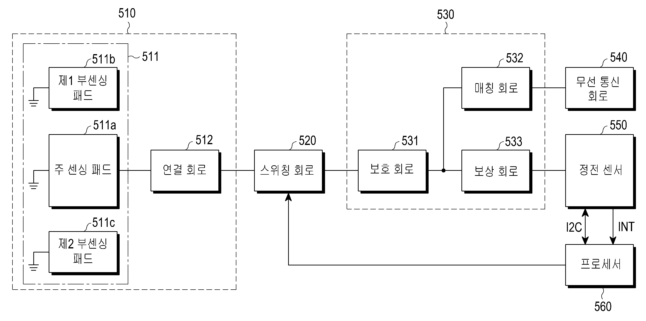
도 5는 본 발명의 다양한 실시 예에 따른 전자 장치의 구성 예를 나타내는 블록도이다. 도 5를 참조하면, 본 발명의 다양한 실시 예에 따른 전자 장치는 적어도 하나의 센싱 패드를 포함하는 센싱 패드부(sensing pad unit)(511), 연결 회로connecting circuit)(512), 스위칭 회로(switching circuit)(520), 보호 회로(protecting circuit)(531), 매칭 회로(impedance matching circuit)(532), 보상 회로(offset compensation circuit)(533), 무선 통신 회로(RF communication circuit)(540), 정전 센서(capacitive sensor)(550), 프로세서(processor)(560) 중 적어도 하나를 포함할 수 있다.5 is a block diagram illustrating a configuration example of an electronic device according to various embodiments of the present disclosure. Referring to FIG. 5 , an electronic device according to various embodiments of the present disclosure includes a
상기 센싱 패드부(511)는 연결 회로(512)에 직접 연결되는 주 센싱 패드(511a) 및 상기 주 센싱 패드(511a)와 각각 미리 설정된 만큼의 공간을 두고 이격된 적어도 하나의 부 센싱 패드(511b, 511c)를 포함하여 구성될 수 있다. 상기 센싱 패드부(511) 및 상기 연결 회로(512) 중 적어도 하나는 외부 정전 용량(external capacitance)(510)을 형성할 수 있다. 또한, 상기 보호 회로(531), 매칭 회로(532) 및 보상 회로(533) 중 적어도 하나는 내부 정전 용량(530)을 형성할 수 있다.The
본 발명의 다양한 실시 예에 따라, 상기 외부 정전 용량(510)을 구성하는 연결 회로(512)와 상기 내부 정전 용량(530)을 구성하는 보호 회로(531)는 스위칭 회로(520)에 의해 연결 또는 차단될 수 있다. 예컨대, 프로세서(560)의 제어 신호에 따라 상기 스위칭 회로(520)는 온(ON) 또는 오프(OFF)될 수 있다.According to various embodiments of the present disclosure, the
상기 센싱 패드부(511)의 각 센싱 패드(511a, 511b, 511c)는 전도성 물질(conductive material)로 구성될 수 있다. 상기 각 센싱 패드(511a, 511b, 511c)는 플레이트(plate) 또는 라인(line) 형태로 구성될 수 있으며, 측정 가능한 정전 용량(capacitance)을 형성할 수 있다. 또한, 전술한 바와 같이 상기 센싱 패드부(511) 중 주 센싱 패드(511a)는 연결 회로(512)와 단일 채널을 통해 직접 연결될 수 있으며, 적어도 하나의 부 센싱 패드(511b, 511c)는 상기 주 센싱 패드(511a)와 미리 설정된 공간만큼(예컨대, 커플링 정전 용량(coupling capacitance)이 형성될 수 있는 거리만큼) 이격되어 배치될 수 있다.Each of the
본 발명의 다양한 실시 예에 따라, 상기 주 센싱 패드(511a), 제1 부 센싱 패드(511b), 또는 제2 부 센싱 패드(511c) 중 적어도 하나는 안테나(또는 안테나 방사체)의 기능을 수행하도록 구성될 수도 있다. 또한, 전자 장치에 구비된 안테나를 센싱 패드로 이용할 수도 있다. 예컨대, 전자 장치의 외부에 노출되거나, 외부와 인접하여 구비되는 금속(metal) 안테나는 본 발명의 다양한 실시 예에 따른 센싱 패드의 기능을 수행할 수도 있다.According to various embodiments of the present disclosure, at least one of the
본 발명의 다양한 실시 예에 따라, 상기 센싱 패드부(511)의 각 센싱 패드(511a, 511b, 511c)는 FPCB(flexible printed circuit board) 형태로서 전자 장치(예컨대, 웨어러블 장치)의 내부에 배치될 수 있으며, 상기 FPCB의 형태로서 무선 충전 코일과 공용으로 설계되는 것도 가능하다.According to various embodiments of the present disclosure, each of the
상기 연결 회로(512)는 접촉 단자(contact terminal)를 통해 상기 주 센싱 패드(511a)와 센서 회로(예컨대, 각종 회로들을 포함하는 회로 기판)를 연결할 수 있다. 상기 연결 회로(512)는 탄성이 있는 구조(예컨대, C-클립)로 구성되거나, 솔더(solder) 또는 커넥터(connector) 결합에 의한 전기적 연결이 가능하며, 특정 재질 또는 형태로 한정되는 것은 아니다.The
상기 스위칭 회로(520)는 상기 프로세서(560)에 의해 연결 회로(512)와 보호 회로(531) 간의 연결을 온/오프시킬 수 있는 적어도 하나의 스위칭 소자를 포함할 수 있다. 본 발명의 다양한 실시 예에 따라, 전자 장치가 비활성인 상태에서는 OFF 상태로 제어되고, 전자 장치가 활성인 상태에서는 ON 상태로 제어될 수 있다.The
상기 도 5에 도시된 바와 같이 상기 스위칭 회로(520)를 기준으로 외부 정전 용량(510) 및 내부 정전 용량(530)으로 구분될 수 있다. 예컨대, 상기 프로세서(560)에 의해 상기 스위칭 회로(520)를 제어함으로써 인위적으로 정전 용량의 차이를 발생시킬 수 있다.As shown in FIG. 5 , the
상기 보호 회로(531)는 DC 블록용 직렬 캐패시터(capacitor), 바리스터(varistor), 다이오드(diode) 중 적어도 하나를 포함하여 구성될 수 있다. 상기 보호 회로(531)는 본 발명의 다양한 실시 예에 따라 상기 주 센싱 패드(511a)를 금속 안테나와 겸하여 사용할 경우, 감전을 방지하는 기능을 제공할 수 있다. 또한, 상기 보호 회로(531)는 정전기에 의한 부품 파손을 방지하는 기능을 제공할 수 있다.The
도 5에 도시된 바와 같이, 정전 센서(550)는 보상 회로(533)를 통해 상기 보호 회로(531)와 연결될 수 있다. 또한, 무선 통신 회로(540)와 연결되는 매칭 회로(532)는 상기 보상 회로(533)와 병렬로 상기 보호 회로(531)와 연결될 수 있다.As shown in FIG. 5 , the
상기 매칭 회로(532)는 상기 주 센싱 패드(511a)를 안테나로 사용할 경우 RF 전송 선로에 대한 임피던스 매칭을 제공할 수 있다. 예컨대, 상기 매칭 회로(532)는 저항, 코일, 캐패시터 중 적어도 하나를 포함하여 구성될 수 있다.The
상기 보상 회로(533)는 센싱 라인의 전체 정전 용량이 정전 센서(550)의 허용 범위를 벗어나는 것을 방지하기 위하여 정전 용량의 보상 기능을 제공할 수 있다. 상기 보상 회로(533)는 적어도 하나의 캐패시터(capacitor)를 포함하여 구성될 수 있다.The
상기 무선 통신 회로(540)는 상기 주 센싱 패드(511a)를 금속 안테나로 사용할 경우, 상기 주 센싱 패드(511a)로부터 수신된 신호를 무선 처리하는 기능을 수행할 수 있다.The
상기 정전 센서(550)는 전술한 바와 같이 정전 용량의 변화를 감지하여 외부 물체에 의한 터치, 근접, 호버링, 그립 등을 판단할 수 있다. 상기 정전 센서(550)는 본 발명의 다양한 실시 예에 따라 캘리브레이션을 수행한 적어도 하나의 임계값을 기준으로 외부 물체를 감지할 수 있다.As described above, the
상기 프로세서(560)는 본 발명의 다양한 실시 예에 따라, 상기 정전 센서(550)로부터 수신된 데이터를 분석하여 대응하는 동작을 수행할 수 있다. 또한, 상기 프로세서(560)는 본 발명의 다양한 실시 예에 따라 스위칭 회로(520)의 온/오프를 제어할 수 있다. 상기 프로세서(560)의 동작에 대한 구체적인 실시 예는 후술하기로 한다.The
전자 장치가 비활성 상태에서 외부 물체가 센싱 패드부(510)에 접촉될 경우, 전자 장치가 활성화 상태로 전환되더라도 상기 외부 물체로 인한 정전 용량의 변화가 발생되지 않아 상기 외부 물체의 접촉 유무를 판단할 수 없게 되는 상황이 발생할 수 있다.When an external object contacts the
본 발명의 다양한 실시 예에 따라, 상기 프로세서(560)는 전자 장치가 비활성 상태일 때 상기 스위칭 회로(520)를 오프 상태로 제어하고, 상기 정전 센서(550)는 활성화시켜 외부 정전 용량(510)을 제외한 내부 정전 용량(530)을 센싱하도록 구현될 수 있다.According to various embodiments of the present disclosure, the
상기 센싱된 내부 정전 용량(530)은 상기 정전 센서(550)의 터치 판단 시 오프셋(offset) 값으로 저장될 수 있으며, 내부 회로 부품 등의 정전 용량 편차로 인해 발생되는 측정값의 편차를 보정할 수 있다.The sensed
또한, 본 발명의 다양한 실시 예에 따라, 상기 프로세서(560)는 전자 장치가 활성화 상태로 전환될 때 상기 스위칭 회로(520)를 온 상태로 제어할 수 있으며, 상기 스위칭 회로(520)의 제어를 통해 상기 정전 센서(550)에서 센싱되는 정전 용량에 내부 정전 용량(530) 또는 외부 정전 용량(510)이 반영되도록 제어할 수 있다.In addition, according to various embodiments of the present disclosure, the
상기 정전 센서(550)는 본 발명의 다양한 실시 예에 따라 자가 정전 용량(self-capacitance) 측정 방식의 터치 센서로 구현될 수 있으며, 상기 프로세서(560)에 의한 스위칭 회로(520)의 제어에 따라, 상기 스위칭 회로(520)가 온 상태일 경우 센싱 패드부(511)의 정전 용량 또는 외부 정전 용량(510)을 측정할 수 있다.The
또한, 본 발명의 다양한 실시 예에 따라, 상기 스위칭 회로(520)가 오프 상태일 경우에는 상기 정전 센서(550)는 상기 센싱 패드부(511)와의 전기적 연결이 차단되고, 회로 부품과 PCB 내부의 스트립 라인(strip-line) 등에 의해 발생된 내부 정전 용량(530)을 측정할 수 있다.Also, according to various embodiments of the present disclosure, when the
이하, 도 6 내지 도 9를 참조하여 상기 도 5에 도시된 회로의 변형된 다양한 실시 예들을 설명하기로 한다. 예컨대, 후술하는 실시 예들에서는 회로 내 구성부의 추가, 삭제, 위치 변화 등을 통해 외부 정전 용량 또는 내부 정전 용량을 다양하게 구성할 수 있다. 후술하는 실시 예들에서도 전술한 도 5의 회로와 마찬가지로 프로세서에 의해 스위칭 회로를 제어함으로써 내부 정전 용량에 대한 오차를 터치 판단에 반영할 수 있다.Hereinafter, various modified embodiments of the circuit shown in FIG. 5 will be described with reference to FIGS. 6 to 9 . For example, in embodiments to be described later, external capacitance or internal capacitance may be configured in various ways by adding, deleting, or changing the position of components in a circuit. In embodiments to be described later, as in the circuit of FIG. 5 described above, an error in internal capacitance may be reflected in a touch determination by controlling a switching circuit by a processor.
예컨대, 연결 회로와 스위칭 회로 사이에 기생 정전 용량을 갖는 소자를 추가로 배치하거나, 스트립 라인(strip line) 설계를 최소화할 수 있다. 또한, 다양한 실시 예에 따라, 스위칭 회로 이후 회로에 기생 정전 용량을 갖는 소자를 배치하거나 스트립 라인 설계를 최대화하여 구성할 수도 있다.For example, an element having parasitic capacitance may be additionally disposed between the connection circuit and the switching circuit, or a strip line design may be minimized. Also, according to various embodiments, an element having parasitic capacitance may be placed in a circuit after the switching circuit or a strip line design may be maximized.
도 6은 본 발명의 다양한 실시 예에 따른 전자 장치의 구성 예를 나타내는 블록도이다. 도 6을 참조하면, 본 발명의 다양한 실시 예에 따른 전자 장치는 적어도 하나의 센싱 패드를 포함하는 센싱 패드부(611), 연결 회로(612), 보호 회로(613), 스위칭 회로(620), 매칭 회로(631), 보상 회로(632), 무선 통신 회로(640), 정전 센서(650), 프로세서(660) 중 적어도 하나를 포함할 수 있다.6 is a block diagram illustrating a configuration example of an electronic device according to various embodiments of the present disclosure. Referring to FIG. 6 , an electronic device according to various embodiments of the present disclosure includes a
상기 센싱 패드부(611)는 연결 회로(612)에 직접 연결되는 주 센싱 패드(611a) 및 상기 주 센싱 패드(611a)와 각각 미리 설정된 만큼의 공간을 두고 이격된 적어도 하나의 부 센싱 패드(611b, 611c)를 포함하여 구성될 수 있다. 상기 센싱 패드부(611), 상기 연결 회로(612), 및 상기 보호 회로(613) 중 적어도 하나는 외부 정전 용량(external capacitance)(610)을 형성할 수 있다. 또한, 매칭 회로(631) 및 보상 회로(632) 중 적어도 하나는 내부 정전 용량(630)을 형성할 수 있다.The
본 발명의 다양한 실시 예에 따라, 상기 외부 정전 용량(610)을 구성하는 보호 회로(613)와 상기 내부 정전 용량(630)을 구성하는 보상 회로(532)는 스위칭 회로(620)에 의해 연결 또는 차단될 수 있다. 예컨대, 프로세서(660)의 제어 신호에 따라 상기 스위칭 회로(620)는 온(ON) 또는 오프(OFF)될 수 있다.According to various embodiments of the present disclosure, the
상기 도 6의 각 구성부들의 기능 중 전술한 도 5의 각 구성부와 동일 또는 유사한 기능을 수행하는 기능들의 중복된 설명은 생략하기로 한다.Among the functions of each component of FIG. 6 , duplicate descriptions of functions performing the same or similar functions as those of each component of FIG. 5 will be omitted.
도 6을 참조하면, 보호 회로(613)를 스위칭 회로(620)의 전단으로 이동시켜, 외부 정전 용량(610)에 포함되도록 구성함으로써, 주 센싱 패드(611a)가 금속 안테나의 역할을 할 경우, 전기적 쇼크(electrical shock)를 방지할 수 있다. 상기 보호 회로(613)의 기생 정전 용량은 도시된 바와 같이 외부 정전 용량(610)에 반영될 수 있다.Referring to FIG. 6 , when the
도 7은 본 발명의 다양한 실시 예에 따른 전자 장치의 구성 예를 나타내는 블록도이다. 도 7을 참조하면, 본 발명의 다양한 실시 예에 따른 전자 장치는 적어도 하나의 센싱 패드를 포함하는 센싱 패드부(711), 연결 회로(712), 보호 회로(713), 스위칭 회로(720), 매칭 회로(730), 무선 통신 회로(740), 보상 회로(751), 정전 센서(760), 프로세서(770) 중 적어도 하나를 포함할 수 있다.7 is a block diagram illustrating a configuration example of an electronic device according to various embodiments of the present disclosure. Referring to FIG. 7 , an electronic device according to various embodiments of the present disclosure includes a
상기 센싱 패드부(711)는 연결 회로(712)에 직접 연결되는 주 센싱 패드(711a) 및 상기 주 센싱 패드(711a)와 각각 미리 설정된 만큼의 공간을 두고 이격된 적어도 하나의 부 센싱 패드(711b, 711c)를 포함하여 구성될 수 있다. 상기 센싱 패드부(711), 상기 연결 회로(712), 및 상기 보호 회로(713) 중 적어도 하나는 외부 정전 용량(external capacitance)(710)을 형성할 수 있다. 또한, 상기 보상 회로(751)는 내부 정전 용량(750)을 형성할 수 있다.The
본 발명의 다양한 실시 예에 따라, 상기 외부 정전 용량(710)을 구성하는 보호 회로(713)와 상기 내부 정전 용량(750)을 구성하는 보상 회로(751) 또는 매칭 회로(730)는 스위칭 회로(720)에 의해 연결 또는 차단될 수 있다. 예컨대, 프로세서(770)의 제어 신호에 따라 상기 스위칭 회로(720)는 상기 보호 회로(713)가 상기 보상 회로(751)와 연결되도록 스위칭할 수도 있으며, 상기 보호 회로(713)가 상기 매칭 회로(730)와 연결되도록 스위칭할 수도 있다.According to various embodiments of the present disclosure, the
상기 도 7의 각 구성부들의 기능 중 전술한 도 5 또는 도 6의 각 구성부와 동일 또는 유사한 기능을 수행하는 기능들의 중복된 설명은 생략하기로 한다.Among the functions of each component of FIG. 7 , duplicate descriptions of functions that perform the same or similar functions as those of each component of FIG. 5 or 6 will be omitted.
도 7을 참조하면, 보호 회로(713)는 도 6에서와 마찬가지로 스위칭 회로(720)의 전단으로 이동시켜, 외부 정전 용량(710)에 포함되도록 구성함으로써, 주 센싱 패드(711a)가 금속 안테나의 역할을 할 경우, 전기적 쇼크(electrical shock)를 방지할 수 있다. 상기 보호 회로(713)의 기생 정전 용량은 도시된 바와 같이 외부 정전 용량(710)에 반영될 수 있다.Referring to FIG. 7 , the
또한, 도 7을 참조하면, 본 발명의 다양한 실시 예에 따라, 스위칭 회로(720)는 무선 통신 회로(740)를 통한 경로와 정전 센서(760)로 흐르는 경로를 분리시킬 수 있다. 예컨대, 상기 주 센싱 패드(711a)가 센서로서의 기능을 수행할 경우, 프로세서(770)는 보호 회로(713)가 보상 회로(751)로 연결되도록 상기 스위칭 회로(720)를 제어할 수 있다. 또한, 상기 주 센싱 패드(711a)가 금속 안테나로서의 기능을 수행할 경우, 프로세서(770)는 보호 회로(713)가 매칭 회로(730)로 연결되도록 상기 스위칭 회로(720)를 제어할 수 있다. 상기 도 7과 같이 회로를 구성할 경우, 내부 정전 용량(750)을 구성하는 기생 정전 용량 소자의 개수를 줄일 수 있다.Also, referring to FIG. 7 , according to various embodiments of the present disclosure, the
도 8은 본 발명의 다양한 실시 예에 따른 전자 장치의 구성 예를 나타내는 블록도이다. 도 8을 참조하면, 본 발명의 다양한 실시 예에 따른 전자 장치는 적어도 하나의 센싱 패드를 포함하는 센싱 패드부(811), 연결 회로(812), 스위칭 회로(820), 보호 회로(831), 간섭 보호 회로(interference protecting circuit)(832), 매칭 회로(833), 보상 회로(834), 무선 통신 회로(840), 정전 센서(850), 프로세서(860) 중 적어도 하나를 포함할 수 있다.8 is a block diagram illustrating a configuration example of an electronic device according to various embodiments of the present disclosure. Referring to FIG. 8 , an electronic device according to various embodiments of the present disclosure includes a
상기 센싱 패드부(811)는 연결 회로(812)에 직접 연결되는 주 센싱 패드(811a) 및 상기 주 센싱 패드(811a)와 각각 미리 설정된 만큼의 공간을 두고 이격된 적어도 하나의 부 센싱 패드(811b, 811c)를 포함하여 구성될 수 있다. 상기 센싱 패드부(811) 및 상기 연결 회로(812) 중 적어도 하나는 외부 정전 용량(external capacitance)(810)을 형성할 수 있다. 또한, 상기 보호 회로(831), 간섭 보호 회로(832), 매칭 회로(833) 및 보상 회로(834) 중 적어도 하나는 내부 정전 용량(830)을 형성할 수 있다.The
본 발명의 다양한 실시 예에 따라, 상기 외부 정전 용량(810)을 구성하는 연결 회로(812)와 상기 내부 정전 용량(830)을 구성하는 보호 회로(831)는 스위칭 회로(820)에 의해 연결 또는 차단될 수 있다. 예컨대, 프로세서(860)의 제어 신호에 따라 상기 스위칭 회로(820)는 온(ON) 또는 오프(OFF)될 수 있다.According to various embodiments of the present disclosure, the
상기 도 8의 각 구성부들의 기능 중 전술한 도 5 또는 도 6의 각 구성부와 동일 또는 유사한 기능을 수행하는 기능들의 중복된 설명은 생략하기로 한다.Among the functions of each component of FIG. 8 , overlapping descriptions of functions performing the same or similar functions as those of each component of FIG. 5 or 6 will be omitted.
도 8을 참조하면, 본 발명의 다양한 실시 예에 따라, 보호 회로(831)와 매칭 회로(833) 사이에 간섭 보호 회로(832)를 추가함으로써 RF 회로와 센서 회로 간의 신호 간섭으로 인해 발생되는 노이즈 신호를 방지할 수 있다.Referring to FIG. 8 , noise generated due to signal interference between an RF circuit and a sensor circuit by adding an
예컨대, 주 센싱 패드(811a)가 센서의 역할을 할 때 스위칭 회로(820) 및 보호 회로(831)를 통해 보상 회로(834) 및 정전 센서(850)로 유입되는 센서 신호와 상기 주 센싱 패드(811a)가 안테나의 역할을 할 때 스위칭 회로(820) 및 보호 회로(831)를 통해 매칭 회로(833) 및 무선 통신 회로(840)로 유입되는 RF 신호를 분리시킴으로서 상호 간의 간섭을 제거할 수 있다. 본 발명의 다양한 실시 예에 따라 상기 간섭 보호 회로(832)는 인덕터(inductor) 또는 비드(bead) 등과 같이 특정 주파수 대역을 필터링하거나 차단시키는 특성을 갖는 소자로 구성될 수 있다.For example, when the
도 9는 본 발명의 다양한 실시 예에 따른 전자 장치의 구성 예를 나타내는 블록도이다. 도 9를 참조하면, 본 발명의 다양한 실시 예에 따른 전자 장치는 적어도 하나의 센싱 패드를 포함하는 센싱 패드부(911), 연결 회로(912), 스위칭 회로(920), 보호 회로(931), 보상 회로(932), 정전 센서(940), 프로세서(950) 중 적어도 하나를 포함할 수 있다.9 is a block diagram illustrating a configuration example of an electronic device according to various embodiments of the present disclosure. Referring to FIG. 9 , an electronic device according to various embodiments of the present disclosure includes a
상기 센싱 패드부(911)는 연결 회로(912)에 직접 연결되는 주 센싱 패드(911a) 및 상기 주 센싱 패드(911a)와 각각 미리 설정된 만큼의 공간을 두고 이격된 적어도 하나의 부 센싱 패드(911b, 911c)를 포함하여 구성될 수 있다. 상기 센싱 패드부(911) 및 상기 연결 회로(912) 중 적어도 하나는 외부 정전 용량(external capacitance)(910)을 형성할 수 있다. 또한, 상기 보호 회로(931), 및 보상 회로(932) 중 적어도 하나는 내부 정전 용량(930)을 형성할 수 있다.The
본 발명의 다양한 실시 예에 따라, 상기 외부 정전 용량(910)을 구성하는 연결 회로(912)와 상기 내부 정전 용량(930)을 구성하는 보호 회로(931)는 스위칭 회로(920)에 의해 연결 또는 차단될 수 있다. 예컨대, 프로세서(960)의 제어 신호에 따라 상기 스위칭 회로(920)는 온(ON) 또는 오프(OFF)될 수 있다.According to various embodiments of the present disclosure, the
상기 도 9의 각 구성부들의 기능 중 전술한 도 5 또는 도 6의 각 구성부와 동일 또는 유사한 기능을 수행하는 기능들의 중복된 설명은 생략하기로 한다.Among the functions of each component of FIG. 9 , overlapping descriptions of functions performing the same or similar functions as those of each component of FIG. 5 or 6 will be omitted.
도 9를 참조하면, 본 발명의 다양한 실시 예에 따라, 전자 장치가 웨어러블 장치의 형태로 구현될 경우, 상기 주 센싱 패드(911a)는 안테나의 기능 없이 센싱 패드로서의 기능만을 수행할 수도 있다. 상기 프로세서(950)는 전술한 바와 같이 정전 센서(940)에 대한 캘리브레이션이 필요할 경우 스위칭 회로(920)를 온/오프 제어함으로써 내부 정전 용량(930) 또는 외부 정전 용량(910)을 판단하고, 상기 판단한 내부 정전 용량(930) 또는 외부 정전 용량(910)을 기반으로 터치 판단을 위한 임계값을 결정할 수 있다.Referring to FIG. 9 , according to various embodiments of the present disclosure, when an electronic device is implemented in the form of a wearable device, the
본 발명의 다양한 실시 예 중 어느 하나에 따른 전자 장치는, 제1 면, 상기 제1 면의 반대로 향하는 제2 면, 및 상기 제1 면 및 제2 면 사이의 공간을 적어도 일부 둘러싸는 측면을 포함하는 하우징; 상기 하우징의 내부에 배치된 무선 통신 회로; 상기 하우징의 제1 면, 제2 면, 및/또는 측면 중 적어도 하나의 적어도 일부를 형성하고, 상기 무선 통신 회로와 전기적으로 연결된 안테나 방사체; 상기 안테나 방사체의 적어도 일부를 형성하거나, 상기 안테나 방사체로부터 이격되어 배치된 제 1 도전성 부재; 상기 하우징의 내부에 배치된 스위칭 회로; 상기 제1 도전성 부재와 상기 스위칭 회로를 통하여 전기적으로 연결 가능하고, 상기 제1 도전성 부재에 대한 외부 물체의 접촉 또는 근접을 감지하도록 구성된 센서; 상기 무선 통신 회로, 상기 스위칭 회로, 및 상기 센서와 전기적으로 연결된 프로세서; 및 상기 프로세서와 전기적으로 연결된 메모리를 포함하고, 상기 메모리는, 실행시에, 상기 프로세서가, 상기 전자 장치의 적어도 일부가 활성화 되었는지 여부를 판단하고, 상기 스위칭 회로를 이용하여, 상기 전자 장치의 적어도 일부가 비활성화 된 경우, 상기 센서와 상기 제1 도전성 부재를 전기적으로 분리하는 제1 상태를 제공하고, 상기 전자 장치의 적어도 일부가 활성화된 경우, 상기 센서와 상기 제1 도전성 부재를 전기적으로 연결하는 제2 상태를 제공하도록 하는 인스트럭션들을 저장할 수 있다.An electronic device according to any one of various embodiments of the present disclosure includes a first surface, a second surface facing opposite to the first surface, and a side surface at least partially enclosing a space between the first surface and the second surface. housing to; a wireless communication circuit disposed inside the housing; an antenna radiator that forms at least a portion of at least one of the first, second, and/or side surfaces of the housing and is electrically connected to the wireless communication circuit; a first conductive member that forms at least a part of the antenna radiator or is spaced apart from the antenna radiator; a switching circuit disposed inside the housing; a sensor electrically connectable to the first conductive member through the switching circuit and configured to detect a contact or proximity of an external object to the first conductive member; a processor electrically connected to the wireless communication circuit, the switching circuit, and the sensor; and a memory electrically connected to the processor, wherein the memory, when executed, determines whether at least a part of the electronic device is activated, and, by using the switching circuit, at least one of the electronic device Providing a first state in which the sensor and the first conductive member are electrically separated when a part is inactivated, and when at least a part of the electronic device is activated, electrically connecting the sensor and the first conductive member It may store instructions to provide the second state.
본 발명의 다양한 실시 예에 따라, 상기 인스트럭션들은, 상기 프로세서가, 상기 센서를 이용하여, 상기 제1 상태에서 제1 데이터를 획득하고, 상기 제2 상태에서 제2 데이터를 획득하도록 할 수 있다.According to various embodiments of the present disclosure, the instructions may cause the processor to obtain first data in the first state and second data in the second state by using the sensor.
본 발명의 다양한 실시 예에 따라, 상기 인스트럭션들은, 상기 프로세서가, 상기 제1 데이터 및 상기 제2 데이터에 적어도 일부 기초하여, 상기 제1 도전성 부재에 대한 사용자의 신체의 접촉 또는 근접 여부를 판단하도록 할 수 있다.According to various embodiments of the present disclosure, the instructions may cause the processor to determine whether the user's body is in contact with or close to the first conductive member based at least in part on the first data and the second data. can do.
본 발명의 다양한 실시 예에 따라, 상기 인스트럭션들은, 상기 프로세서가, 상기 제1 데이터 및 상기 제2 데이터의 차이가 쓰레쉬홀드 값 미만인 경우, 상기 제1 도전성 부재로부터 상기 사용자의 신체가 이격되었다고 판단하고, 상기 제1 데이터 및 상기 제2 데이터의 차이가 상기 쓰레쉬홀드 값 이상인 경우, 상기 제1 도전성 부재에 상기 사용자의 신체가 접촉 또는 근접하다고 판단하도록 할 수 있다.According to various embodiments of the present disclosure, in the instructions, the processor determines that the user's body is separated from the first conductive member when a difference between the first data and the second data is less than a threshold value. and when the difference between the first data and the second data is greater than or equal to the threshold value, it may be determined that the user's body is in contact with or close to the first conductive member.
본 발명의 다양한 실시 예에 따라, 상기 인스트럭션들은, 상기 프로세서가, 상기 제1 데이터에 적어도 일부 기초하여, 상기 제 2 데이터를 보정하고, 상기 보정된 제 2 데이터에 적어도 일부 기초하여, 상기 제 1 도전성 부재에 대한 사용자의 신체의 접촉 또는 근접 여부를 판단하도록 할 수 있다.According to various embodiments of the present disclosure, the instructions may cause the processor to correct the second data based at least in part on the first data, and based on at least a portion of the corrected second data, to perform the correcting of the first data. It is possible to determine whether the user's body is in contact or proximity to the conductive member.
본 발명의 다양한 실시 예에 따라, 상기 전자 장치는, 상기 스위칭 회로 및 상기 센서 사이에 전기적으로 연결되고, 상기 제1 데이터를 적어도 일부 저장하도록 구성된 보상 회로를 더 포함하고, 상기 인스트럭션들은, 상기 프로세서가, 상기 보상 회로를 이용하여, 상기 제2 데이터를 보정하도록 할 수 있다.According to various embodiments of the present disclosure, the electronic device further includes a compensation circuit electrically connected between the switching circuit and the sensor and configured to store at least a portion of the first data, and the instructions include: the processor The second data may be corrected using the compensation circuit.
본 발명의 다양한 실시 예에 따라, 상기 회로는 상기 도전성 부재를 통하여 감지된 상기 전자 장치의 주변 온도에 기초하여, 상기 외부 물질의 상기 온도를 보정하도록 구성될 수 있다.According to various embodiments of the present disclosure, the circuit may be configured to correct the temperature of the external material based on the ambient temperature of the electronic device sensed through the conductive member.
본 발명의 다양한 실시 예에 따라, 상기 전자 장치는, 상기 제1 도전성 부재로부터 절연된 제2 도전성 부재를 더 포함할 수 있다.According to various embodiments of the present disclosure, the electronic device may further include a second conductive member insulated from the first conductive member.
본 발명의 다양한 실시 예에 따라, 상기 제1 도전성 부재 및 상기 제 2 도전성 부재 사이에 형성된 캐패시턴스 CC, 상기 제1 도전성 부재 및/또는 상기 제2 도전성 부재와, 사용자의 신체 사이에 형성된 캐패시턴스 Cf, 상기 제1 도전성 부재에서 형성된 기생 캐패시턴스 CP1, 및 상기 제2 도전성 부재에서 형성된 기생 캐패시턴스 CP2 는, CP1> CP2, Cf≥≥CP2, 또는 Cf≤≤Cc 중 적어도 하나의 관계를 만족할 수 있다.According to various embodiments of the present disclosure, a capacitance C C formed between the first conductive member and the second conductive member, a capacitance C formed between the first conductive member and/or the second conductive member and the user's body f , the parasitic capacitance C P1 formed in the first conductive member, and the parasitic capacitance C P2 formed in the second conductive member are at least C P1 > C P2 , C f ≥≥ C P2 , or C f ≤≤ C c One relationship can be satisfied.
본 발명의 다양한 실시 예에 따라, 상기 전자 장치는, 상기 제1 도전성 부재 및 상기 제2 도전성 부재로부터 절연된, 제3 도전성 부재를 더 포함할 수 있다.According to various embodiments of the present disclosure, the electronic device may further include a third conductive member insulated from the first conductive member and the second conductive member.
본 발명의 다양한 실시 예에 따라, 상기 제1 도전성 부재 및 상기 제2 도전성 부재 사이에 형성된 캐패시턴스 CC1, 상기 제1 도전성 부재 및 상기 제3 도전성 부재 사이에 형성된 캐패시턴스 CC2, 상기 제2 도전성 부재 및 상기 제3 도전성 부재 사이에 형성된 캐패시턴스 CC3, 상기 제1 도전성 부재, 상기 제2 도전성 부재, 및/또는 상기 제3 도전성 부재와 사용자의 신체 사이에 형성된 캐패시턴스 Cf, 상기 제1 도전성 부재에서 형성된 기생 캐패시턴스 CP1, 상기 제2 도전성 부재에서 형성된 기생 캐패시턴스 CP2, 및 상기 제3 도전성 부재에서 형성된 기생 캐패시턴스 CP3 는, CP1> CP2 or CP3, Cf≥≥CP2 or CP3, Cf≤≤Cc1 or CC2, CP2≠CP3, 또는 Cc1≠Cc2≠Cc3 중 적어도 하나의 관계를 만족할 수 있다.According to various embodiments of the present disclosure, a capacitance C C1 formed between the first conductive member and the second conductive member, a capacitance C C2 formed between the first conductive member and the third conductive member, and a capacitance C C2 formed between the second conductive member and a capacitance C C3 formed between the third conductive member, a capacitance C f formed between the first conductive member, the second conductive member, and/or the third conductive member and the user's body, in the first conductive member. The formed parasitic capacitance C P1 , the parasitic capacitance C P2 formed in the second conductive member, and the parasitic capacitance C P3 formed in the third conductive member are: C P1 > C P2 or C P3 , C f ≥≥C P2 or C P3 , C f ≤≤C c1 or C C2 , C P2 ≠ C P3 , or C c1 ≠ C c2 ≠ C c3 .
본 발명의 다양한 실시 예에 따라, 상기 전자 장치는, 상기 하우징 내부에 배치된 인쇄회로기판; 및 상기 제1 도전성 부재와 인쇄회로기판 사이에 전기적으로 연결된 연결 부재를 더 포함할 수 있다.According to various embodiments of the present disclosure, the electronic device may include a printed circuit board disposed inside the housing; and a connection member electrically connected between the first conductive member and the printed circuit board.
본 발명의 다양한 실시 예에 따라, 상기 무선 통신 회로, 상기 센서, 상기 스위칭 회로, 상기 프로세서, 또는 상기 메모리 중 적어도 하나는 상기 인쇄회로기판에 배치될 수 있다.According to various embodiments of the present disclosure, at least one of the wireless communication circuit, the sensor, the switching circuit, the processor, and the memory may be disposed on the printed circuit board.
본 발명의 다양한 실시 예에 따라, 상기 전자 장치는, 상기 인쇄회로기판 및 상기 제1 도전성 부재 사이에 전기적으로 연결되고, 상기 안테나 방사체에 인가되어 상기 인쇄회로기판으로 유입되는 정전기를 적어도 일부 차단하도록 구성된 보호 회로를 더 포함할 수 있다.According to various embodiments of the present disclosure, the electronic device is electrically connected between the printed circuit board and the first conductive member, and is applied to the antenna radiator to at least partially block static electricity flowing into the printed circuit board. It may further include a configured protection circuit.
본 발명의 다양한 실시 예에 따라, 상기 스위칭 회로는, 적어도 하나의 트랜지스터를 포함하고, 상기 적어도 하나의 트랜지스터에 인가된 적어도 하나의 신호에 기초하여 스위칭하도록 구성될 수 있다.According to various embodiments of the present disclosure, the switching circuit may include at least one transistor and may be configured to switch based on at least one signal applied to the at least one transistor.
본 발명의 다양한 실시 예에 따라, 상기 센서는, 상기 센서로부터 발생되어, 상기 제1 도전성 부재를 통하여 돌아온 신호에 기초하여, 상기 제1 도전성 부재 및 외부 물체 사이에 형성된 정전용량의 변화를 검출하도록 구성될 수 있다.According to various embodiments of the present disclosure, the sensor is configured to detect a change in capacitance formed between the first conductive member and an external object based on a signal generated from the sensor and returned through the first conductive member. can be configured.
본 발명의 다양한 실시 예 중 어느 하나에 따른 전자 장치는, 제1 면, 상기 제1 면의 반대로 향하는 제2 면, 및 상기 제1 면 및 제2 면 사이의 공간을 적어도 일부 둘러싸는 측면을 포함하는 하우징; 상기 하우징의 내부에 배치된 무선 통신 회로; 상기 하우징의 제1 면, 제2 면, 및/또는 측면 중 적어도 하나의 적어도 일부를 형성하고, 상기 무선 통신 회로와 전기적으로 연결된 안테나 방사체; 상기 안테나 방사체에 외부 물체의 접촉 또는 근접을 감지하도록 구성된 센서; 상기 안테나 방사체에 전기적으로 연결된 제1 단자, 및 상기 센서에 전기적으로 연결된 제2 단자를 포함하는 스위칭 회로; 상기 센서 및 상기 스위칭 회로와 전기적으로 연결된 프로세서; 및 상기 프로세서와 전기적으로 연결된 메모리를 포함하고, 상기 메모리는, 실행시에, 상기 프로세서가,상기 스위칭 회로에 의하여, 상기 안테나 방사체 및 상기 센서가 전기적으로 연결될 때, 상기 센서로부터의 제1 측정 값(measurement value)을 수신하고, 상기 스위칭 회로에 의하여, 상기 안테나 방사체 및 상기 센서가 전기적으로 분리될 때, 상기 센서로부터의 제2 측정 값을 수신하도록 하는 인스트럭션들을 저장할 수 있다.An electronic device according to any one of various embodiments of the present disclosure includes a first surface, a second surface facing opposite to the first surface, and a side surface at least partially enclosing a space between the first surface and the second surface. housing to; a wireless communication circuit disposed inside the housing; an antenna radiator that forms at least a portion of at least one of the first, second, and/or side surfaces of the housing and is electrically connected to the wireless communication circuit; a sensor configured to detect contact or proximity of an external object to the antenna radiator; a switching circuit including a first terminal electrically connected to the antenna radiator and a second terminal electrically connected to the sensor; a processor electrically connected to the sensor and the switching circuit; and a memory electrically connected to the processor, wherein the memory, when executed, causes the processor to, by the switching circuit, when the antenna radiator and the sensor are electrically connected, a first measurement value from the sensor It may store instructions for receiving a measurement value and receiving a second measurement value from the sensor when the antenna radiator and the sensor are electrically separated by the switching circuit.
본 발명의 다양한 실시 예에 따라, 상기 인스트럭션들은, 상기 프로세서가, 상기 제2 측정 값을 상기 메모리 상에 적어도 임시로 저장할 수 있다.According to various embodiments of the present disclosure, in the instructions, the processor may at least temporarily store the second measurement value in the memory.
본 발명의 다양한 실시 예에 따라, 상기 인스트럭션들은, 상기 프로세서가, 상기 제1 측정 값 및 제2 측정 값을 이용하여, 외부 물체가 상기 안테나 방사체에 접촉 또는 근접하였는지를 결정하도록 할 수 있다.According to various embodiments of the present disclosure, the instructions may cause the processor to determine whether an external object has contacted or approached the antenna radiator by using the first measurement value and the second measurement value.
본 발명의 다양한 실시 예에 따라, 상기 무선 통신 회로는 임피던스 매칭 회로를 포함하고, 상기 임피던스 매칭 회로는 상기 스위칭 회로의 제2 단자에 전기적으로 연결될 수 있다.According to various embodiments of the present disclosure, the wireless communication circuit may include an impedance matching circuit, and the impedance matching circuit may be electrically connected to the second terminal of the switching circuit.
본 발명의 다양한 실시 예 중 어느 하나에 따른 전자 장치는, 도전성 물질로 구성된 적어도 하나의 센싱 패드; 상기 센싱 패드를 통해 판단된 값에 의해 상기 센싱 패드에 대한 물체의 터치 또는 근접을 센싱하는 정전 센서; 상기 센싱 패드와 상기 정전 센서 사이에 연결되는 스위칭 회로; 및 미리 설정된 조건에 따라 상기 스위칭 회로의 온 또는 오프 상태를 제어하는 프로세서;를 포함할 수 있다.An electronic device according to any one of various embodiments of the present disclosure may include at least one sensing pad made of a conductive material; an electrostatic sensor that senses a touch or proximity of an object to the sensing pad based on a value determined through the sensing pad; a switching circuit connected between the sensing pad and the electrostatic sensor; and a processor controlling an on or off state of the switching circuit according to a preset condition.
본 발명의 다양한 실시 예에 따라, 상기 프로세서는, 상기 전자 장치가 비활성 상태일 경우, 상기 스위칭 회로를 오프 상태로 제어할 수 있다.According to various embodiments of the present disclosure, when the electronic device is in an inactive state, the processor may control the switching circuit to be turned off.
본 발명의 다양한 실시 예에 따라, 상기 프로세서는, 상기 전자 장치가 비활성 상태일 경우, 상기 정전 센서로부터 내부 정전 용량을 판단할 수 있다.According to various embodiments of the present disclosure, the processor may determine internal capacitance from the electrostatic sensor when the electronic device is in an inactive state.
본 발명의 다양한 실시 예에 따라, 상기 프로세서는, 상기 판단한 내부 정전 용량으로부터 상기 정전 센서의 측정 값 보정을 위한 오프셋 값을 결정할 수 있다.According to various embodiments of the present disclosure, the processor may determine an offset value for correcting the measured value of the capacitance sensor from the determined internal capacitance.
본 발명의 다양한 실시 예에 따라, 상기 전자 장치는, 상기 정전 센서와 상기 스위칭 회로를 통해 연결되는 주 센싱 패드; 및 상기 주 센싱 패드와 미리 설정된 거리만큼 이격하여 배치되는 적어도 하나의 부 센싱 패드;를 포함할 수 있다.According to various embodiments of the present disclosure, the electronic device may include a main sensing pad connected to the electrostatic sensor through the switching circuit; and at least one sub-sensing pad disposed apart from the main sensing pad by a preset distance.
본 발명의 다양한 실시 예에 따라, 상기 부 센싱 패드는 상기 주 센싱 패드와 미리 설정된 커플링 정전 용량이 형성되는 거리만큼 이격하여 배치될 수 있다.According to various embodiments of the present disclosure, the sub sensing pad may be spaced apart from the main sensing pad by a distance at which a preset coupling capacitance is formed.
본 발명의 다양한 실시 예에 따라, 상기 센싱 패드는 안테나로 사용되며, 상기 전자 장치는, 상기 스위칭 회로와 상기 정전 센서 사이에서 상기 정전 센서와 병렬 연결되고, 상기 센싱 패드를 통해 수신된 무선 신호를 처리하는 무선 통신 회로;를 더 포함할 수 있다.According to various embodiments of the present disclosure, the sensing pad is used as an antenna, and the electronic device is connected in parallel with the electrostatic sensor between the switching circuit and the electrostatic sensor, and transmits a wireless signal received through the sensing pad. A wireless communication circuit for processing; may further include.
본 발명의 다양한 실시 예에 따라, 상기 프로세서는, 상기 스위칭 회로와 상기 무선 통신 회로 사이에 간섭 보호 회로;를 더 포함할 수 있다.According to various embodiments of the present disclosure, the processor may further include an interference protection circuit between the switching circuit and the wireless communication circuit.
본 발명의 다양한 실시 예에 따라, 상기 간섭 보호 회로는, 캐패시터, 배리스터, 또는 다이오드 중 적어도 하나를 포함할 수 있다.According to various embodiments of the present disclosure, the interference protection circuit may include at least one of a capacitor, a varistor, and a diode.
본 발명의 다양한 실시 예에 따라, 상기 전자 장치는, 상기 스위칭 회로와 상기 정전 센서 사이에서 정전 용량이 임계값을 벗어나는 것을 방지하기 위한 보상 회로;를 더 포함할 수 있다.According to various embodiments of the present disclosure, the electronic device may further include a compensation circuit for preventing capacitance between the switching circuit and the electrostatic sensor from deviating from a threshold value.
이하, 도 10을 참조하여, 전술한 각 회로들에서 프로세서(660, 770, 860, 950)가 스위칭 회로(620, 720, 820, 920)를 제어하기 위한 조건 및 상황에 대한 다양한 실시 예들을 상세히 설명한다.Hereinafter, with reference to FIG. 10 , various embodiments of conditions and circumstances for the
도 10은 본 발명의 다양한 실시 예에 따른 스위칭 회로의 동작 스케줄링을 나타내는 도면이다. 도 10을 참조하면, 상기 스위칭 회로는 센싱 패드에 무선 통신 회로가 연결되는지 여부에 따라 온/오프 시점의 트리거(trigger)가 달라질 수 있다.10 is a diagram illustrating operation scheduling of a switching circuit according to various embodiments of the present disclosure. Referring to FIG. 10 , the switching circuit may have a trigger at an on/off time depending on whether a wireless communication circuit is connected to a sensing pad.
예컨대, 상기 센싱 패드에 RF 회로가 연결되어 있는 경우, 단말과 기지국 간의 아이들(idle) 주기에 영향을 받을 수 있다. 본 발명의 다양한 실시 예에 따라 상기 스위칭 회로의 온/오프 시점은 RF 회로의 온/오프 시점과 연동되어, RF 회로가 오프 되는 시점 또는 슬립 모드에 들어가는 시점 동안 스위치가 온 상태가 될 수 있다. 다시 RF 회로가 온 되는 시점 또는 아이들 모드에 들어가는 시점 동안 스위칭 회로는 오프 상태가 될 수 있다.For example, when an RF circuit is connected to the sensing pad, it may be affected by an idle period between a terminal and a base station. According to various embodiments of the present disclosure, the on/off timing of the switching circuit may be interlocked with the on/off timing of the RF circuit, so that the switch may be in an on state when the RF circuit is turned off or enters a sleep mode. The switching circuit may be in an off state at a time when the RF circuit is turned on again or at a time when the RF circuit enters an idle mode.
이러한 스위칭 회로의 온/오프 시점을 RF 회로의 매 아이들/슬립 주기에 맞춰서 진행할 경우, 소모 전류가 높기 때문에 독립적인 주기에 따라 긴 주기 시간 간격에 따라 온/오프될 수도 있다.If the switching circuit is turned on/off according to every idle/sleep period of the RF circuit, it may be turned on/off according to a long cycle time interval according to an independent cycle because current consumption is high.
또한, 본 발명의 다양한 실시 예에 따라 웨어러블 장치와 같이 RF 회로와 연결되지 않는 경우, RF 회로의 온/오프 시점이 아닌 프로세서의 온/오프 시점과 연동될 수 있다.In addition, according to various embodiments of the present disclosure, if it is not connected to an RF circuit like a wearable device, it may be interlocked with the on/off timing of the processor instead of the on/off timing of the RF circuit.
또한, 본 발명의 다양한 실시 예에 따라 스위칭 회로는 화면이 꺼져있느냐, 켜져 있느냐에 따라 온/오프 시점의 트리거(trigger)가 결정될 수 있다. 예컨대, 프로세서가 온이 되는 순간 스위칭 회로가 온이 되고, 프로세서가 오프 상태가 되는 순간, 스위칭 회로가 오프되며, 전술한 바와 같이 내부 정전 용량을 측정하여 보상할 수 있다.Also, according to various embodiments of the present disclosure, a trigger of an on/off time of the switching circuit may be determined depending on whether the screen is off or on. For example, the switching circuit is turned on when the processor is turned on, and the switching circuit is turned off when the processor is turned off. As described above, the internal capacitance may be measured and compensated for.
*전술한 바를 표로 나타내면 하기 <표 3> 및 <표 4>와 같이 나타낼 수 있다. <표 3>은 도 6 내지 도 8에 도시된 바와 같이 RF 회로가 구비된 실시 예에 대응할 수 있으며, <표 4>는 도 9에 도시된 바와 같이 RF 회로가 구비되지 않은 실시 예에 대응할 수 있다.* The above can be expressed as Table 3 and Table 4 below. <Table 3> may correspond to an embodiment with an RF circuit as shown in FIGS. 6 to 8 , and <Table 4> may correspond to an embodiment without an RF circuit as shown in FIG. 9 . there is.
Component
(내부 Capacitance 측정)Status #1
(internal capacitance measurement)
(외부 Capacitance 측정)Status #2
(external capacitance measurement)
Component
(내부 Capacitance 측정)Status #1
(internal capacitance measurement)
(외부 Capacitance 측정)Status #2
(external capacitance measurement)
이하, 도 11 내지 도 19를 참조하여, 전술한 전자 회로의 각 구성부들이 전자 장치 또는 웨어러블 장치 등에 구현된 다양한 실시 예들을 설명하기로 한다.Hereinafter, with reference to FIGS. 11 to 19 , various embodiments in which each component of the electronic circuit described above is implemented in an electronic device or a wearable device will be described.
전술한 센싱 패드부 또는 각 센싱 패드들은 다양한 형태로 구성될 수 있으며, 상기 각 센싱 패드들은 전자 장치의 접지부(ground)에 연결될 수 있다.The aforementioned sensing pad unit or each sensing pad may be configured in various forms, and each sensing pad may be connected to a ground of an electronic device.
후술하는 본 발명의 다양한 실시 예들에서는 전자 장치의 외부 하우징을 이용하여 센싱 패드를 구성하거나, 상기 전자 장치의 외부 하우징과 인접한 상기 전자 장치의 내부에 FPCB 형태로 센싱 패드를 구성할 수도 있다. 상기 센싱 패드가 하우징의 일부를 이용하여 구성할 경우, 복수의 연결 회로가 존재할 수도 있으며, 상기 복수의 연결 회로들 중 적어도 하나의 연결 회로를 통해 접지부와 연결될 수 있다.In various embodiments of the present disclosure described below, a sensing pad may be configured using an external housing of the electronic device, or a sensing pad may be configured in an FPCB type inside the electronic device adjacent to the external housing of the electronic device. When the sensing pad is configured using a part of the housing, a plurality of connection circuits may exist, and may be connected to a ground through at least one connection circuit among the plurality of connection circuits.
도 11은 본 발명의 다양한 실시 예에 따른 전자 장치의 부품 실장 구조를 나타내는 도면이다. 도 11을 참조하면, 전자 장치의 하우징의 일부가 금속 안테나로 구성될 경우, 상기 하우징의 적어도 일부는 주 센싱 패드(1101a), 제1 부 센싱 패드(1101b), 제2 부 센싱 패드(1101c)를 구성할 수 있다. 상기 각 부 센싱 패드(1101b, 1101c)는 상기 주 센싱 패드(1101a)와 미리 설정된 공간(예컨대, 커플링 영역)을 두고 이격되도록 구성될 수 있다. 또한, 본 발명의 다양한 실시 예에 따라, 상기 주 센싱 패드(1101a)와 각 부 센싱 패드(1101b, 1101c) 사이에는 유전체로 구성될 수도 있다. 후술하는 도 11의 회로 구성은 도 5의 블록도에 대응할 수 있다.11 is a diagram illustrating a component mounting structure of an electronic device according to various embodiments of the present disclosure. Referring to FIG. 11 , when a part of a housing of an electronic device is configured as a metal antenna, at least a part of the housing includes a
상기 하우징의 내부에는 연결 회로(1110), 스위칭 회로(1120), 보호 회로(1130), 매칭 회로(1140), 보상 회로(1150), 무선 통신 회로(1160), 정전 센서(1170)를 포함하여 구성될 수 있다. 상기 주 센싱 패드(1101a)는 연결 회로(1110)를 거쳐 스위칭 회로(1120)에 연결될 수 있다. 스위칭 회로(1120)는 프로세서의 제어 신호에 따라 온 또는 오프 상태로 제어될 수 있다. 상기 하우징 내부에 구성된 각 회로들은 PCB 상에서 구현될 수 있다.The inside of the housing includes a
상기 도 11에서 상기 금속 하우징의 일부를 구성하는 주 센싱 패드(1101a)는 연결 회로(1110)를 통해 내부 부품들과 전기적으로 연결될 수 있다. 또한, 본 발명의 다양한 실시 예에 따라, 상기 각 센싱 패드들(1101a, 1101b, 1101c))은 FPCB 형태로 구성되어 솔더(solder) 또는 커넥터(connector) 등과 같은 연결 회로에 의해 PCB와 결합될 수도 있다.In FIG. 11 , the
전술한 바와 같이 상기 스위칭 회로(1120)의 일 단은 연결 회로(1110)를 통해 주 센싱 패드(1101a)와 직접적으로 연결될 수 있으며, 상기 스위칭 회로(1120)의 타 단은 다른 회로 부품들과 연결되도록 구현될 수 있다.As described above, one end of the
도 12는 본 발명의 다양한 실시 예에 따른 전자 장치의 부품 실장 구조를 나타내는 도면이다. 도 12를 참조하면, 전자 장치의 하우징의 일부가 금속 안테나로 구성될 경우, 상기 하우징의 적어도 일부는 주 센싱 패드(1201a), 제1 부 센싱 패드(1201b), 제2 부 센싱 패드(1201c)를 구성할 수 있다. 상기 각 부 센싱 패드(1201b, 1201c)는 상기 주 센싱 패드(1201a)와 미리 설정된 공간(예컨대, 커플링 영역)을 두고 이격되도록 구성될 수 있다. 또한, 본 발명의 다양한 실시 예에 따라, 상기 주 센싱 패드(1201a)와 각 부 센싱 패드(1201b, 1201c) 사이에는 유전체로 구성될 수도 있다. 후술하는 도 12의 회로 구성은 도 6의 블록도에 대응할 수 있다.12 is a diagram illustrating a component mounting structure of an electronic device according to various embodiments of the present disclosure. Referring to FIG. 12 , when a part of a housing of an electronic device is configured as a metal antenna, at least a part of the housing includes a
상기 하우징의 내부에는 연결 회로(1210), 보호 회로(1220), 스위칭 회로(1230), 매칭 회로(1240), 보상 회로(1250), 무선 통신 회로(1260), 정전 센서(1270)를 포함하여 구성될 수 있다. 상기 주 센싱 패드(1201a)는 연결 회로(1210) 및 보호 회로(1220)를 거쳐 스위칭 회로(1230)에 연결될 수 있다. 스위칭 회로(1230)는 프로세서의 제어 신호에 따라 온 또는 오프 상태로 제어될 수 있다. 상기 하우징 내부에 구성된 각 회로들은 PCB 상에서 구현될 수 있다.The inside of the housing includes a
상기 도 12에서 상기 금속 하우징의 일부를 구성하는 주 센싱 패드(1201a)는 연결 회로(1210)를 통해 내부 부품들과 전기적으로 연결될 수 있다. 또한, 본 발명의 다양한 실시 예에 따라, 상기 각 센싱 패드들(1101a, 1101b, 1101c))은 FPCB 형태로 구성되어 솔더(solder) 또는 커넥터(connector) 등과 같은 연결 회로에 의해 PCB와 결합될 수도 있다.In FIG. 12 , the
전술한 바와 같이 상기 스위칭 회로(1230)의 일 단은 보호 회로(1220) 및 연결 회로(1210)를 통해 주 센싱 패드(1201a)와 직접적으로 연결될 수 있으며, 상기 스위칭 회로(1230)의 타 단은 다른 회로 부품들과 연결되도록 구현될 수 있다.As described above, one end of the
도 12에 도시된 바와 같이 스위칭 회로(1230)의 입력단에 보호 회로(1220)를 배치할 수 있다. 상기 도 12와 같이 구현할 경우, 주 센싱 패드(1201a)와 스위칭 회로(1230) 사이에 위치한 회로 부품(예컨대, 보호 회로(1220))의 기생 정전 용량으로 인해, 정전 센서(1270)에서 측정되는 외부 정전 용량의 측정 편차를 최소화할 필요가 있다. 본 발명의 다양한 실시 예들에서는 회로 부품의 정전 용량 편차에 의한 내부 정전 용량을 최대한 오프셋 값에 반영함으로써 정전 센서의 정확도를 높일 수 있다.As shown in FIG. 12 , a
후살하는 본 발명의 다양한 실시 예에 따라 회로 구성을 PCB 및 FPCB로 분리하여 구성할 수 있다. 예컨대, 프로세서 및 무선 통신 회로는 PCB에 구성하고, 나머지 회로 구성들은 FPCB에 구성할 수 있다.According to various embodiments of the present invention to be described later, the circuit configuration can be configured by separating the PCB and FPCB. For example, a processor and a wireless communication circuit may be configured on a PCB, and other circuit components may be configured on an FPCB.
도 13은 본 발명의 다양한 실시 예에 따른 전자 장치의 부품 실장 구조를 나타내는 도면이다. 도 13을 참조하면, 주 센싱 패드(1301a), 제1 부 센싱 패드(1301b), 제2 부 센싱 패드(1301c)는 하우징의 적어도 일부를 구성할 수 있으며, 각 센싱 패드들은 커플링 영역(coupling area)(1302a, 1302b)을 사이에 두고 서로 구분될 수 있다.13 is a diagram illustrating a component mounting structure of an electronic device according to various embodiments of the present disclosure. Referring to FIG. 13 , the
상기 주 센싱 패드(1301a)는 하우징 내부의 FPCB에 구성된 연결 회로(1380)를 통해 스위칭 회로(1370)와 연결될 수 있다. 상기 FPCB에는 연결 회로(1380), 스위칭 회로(1370), 보호 회로(1360), 매칭 회로(1350), 보상 회로(1340), 정전 센서(1330)가 배치될 수 있다.The
예컨대, 상기 보호 회로(1360)에서는 병렬로 분기하여 보상 회로(1340) 및 매칭 회로(1350)가 연결될 수 있다. 상기 보상 회로(1340)는 정전 센서(1330)와 연결되고, 상기 정전 센서(1330)는 PCB에 배치된 프로세서(1310)와 연결될 수 있다. 또한, 상기 FPCB는 커넥터를 통해 PCB 회로와 전기적으로 연결될 수 있으며, 상기 매칭 회로(1350)는 무선 동축 케이블(RF coaxial cable)을 통해 PCB에 배치된 무선 통신 회로(1320)에 연결될 수 있다. 상기 도 13에서 자가 정전 용량(self-capacitance)의 생성을 위해 연결 회로(1380) 중 적어도 하나는 FPCB나 PCB 상의 접지부(ground)와 연결될 수 있다.For example, in the
이하, 도 14 내지 도 19를 참조하여, 본 발명의 다양한 실시 예들이 웨어러블 장치(예컨대, 시계형 웨어러블 장치)에 구현될 실시 예들을 설명하기로 한다.Hereinafter, various embodiments of the present invention will be described with reference to FIGS. 14 to 19 , which will be implemented in a wearable device (eg, a watch-type wearable device).
도 14는 본 발명의 다양한 실시 예에 따른 웨어러블 장치의 부품 실장 구조를 나타내는 도면이다. 도 14를 참조하면, 웨어러블 장치의 몸체(1400) 내부 바닥면에는 무선 충전 코일(wireless charging coil)(1410), 접촉 패드(contact pad)(1420), 센싱 패드(sensing pad)(1431), 접촉 단자(contact terminal)(1430)를 포함하여 구성할 수 있다.14 is a diagram illustrating a component mounting structure of a wearable device according to various embodiments of the present disclosure. 14, a
도 15는 본 발명의 다양한 실시 예에 따른 웨어러블 장치의 부품 실장 구조를 나타내는 도면이다. 도 15를 참조하면, 도 14에 도시된 센싱 패드는 주 센싱 패드(1531a) 및 적어도 하나의 부 센싱 패드(1531b, 1531c)로 구분되어 구성될 수 있다.15 is a diagram illustrating a component mounting structure of a wearable device according to various embodiments of the present disclosure. Referring to FIG. 15 , the sensing pad shown in FIG. 14 may be configured by being divided into a
예컨대, 단일 감지 채널로 연결된 주 센싱 패드와 일정 간격 분리된 부 센싱 패드로 구성된 센싱 패드 구조는 도시된 바와 같이 웨어러블 장치와 같은 초소형 장치 설계에 있어 최적화된 구조일 수 있다. 상기 웨어러블 장치는 인체 착용을 위해 초소형으로 설계되기 때문에, 상기 센싱 패드와 인쇄 회로 기판(PCB)을 전기적으로 연결하기 위한 접촉 터미널 또는 솔더 패드(solder pad)의 실장 공간 확보가 어려울 수 있다. 도 15에서는 이러한 구조를 최적화하여 웨어러블 장치의 몸체(1500) 내에 실장할 수 있다.For example, a sensing pad structure composed of a main sensing pad connected by a single sensing channel and sub sensing pads separated by a predetermined distance may be an optimized structure for designing a subminiature device such as a wearable device. Since the wearable device is designed to be worn on a human body, it may be difficult to secure a mounting space for a contact terminal or a solder pad for electrically connecting the sensing pad and a printed circuit board (PCB). In FIG. 15, this structure can be optimized and mounted in the
도 15를 참조하면, 웨어러블 장치의 몸체(1500) 내부 바닥면에는 무선 충전 코일(1510), 접촉 패드(1520), 복수의 센싱 패드들(1531a, 1531b, 1531c)을 포함하여 구성할 수 있다.Referring to FIG. 15 , a
도 16은 본 발명의 다양한 실시 예에 따른 웨어러블 장치의 부품 실장 구조를 나타내는 도면이다. 도 16을 참조하면, 웨어러블 장치의 몸체(1600) 내에 FPCB(1620)가 실장되며, 상기 FPCB(1620)는 PCB의 접촉 터미널(1630)과 연결될 수 있다. 본 발명의 다양한 실시 예에 따라, 복수의 센싱 패드들은 상기 몸체(1600)의 하부 바닥면에 구비될 수 있으며, 상기 FPCB의 적어도 일부인 접촉 패드와 접촉될 수 있다. 상기 몸체(1600)의 바닥면에는 윈도우 데코(window deco)(1640)가 더 구비될 수 있다. 16 is a diagram illustrating a component mounting structure of a wearable device according to various embodiments of the present disclosure. Referring to FIG. 16 , an
상기 도 16에 도시된 웨어러블 장치에서 원형 FPCB의 센싱 패드를 실장하고, 주 센싱 패드 및 부 센싱 패드의 분리된 구조를 형성함으로써 웨어러블 장치의 다양한 사용자 착용 상태를 인식할 수 있다. 예컨대, 본 발명의 다양한 실시 예에 따라 주 센싱 패드 및 적어도 하나의 부 센싱 패드를 포함하는 센싱 패드부를 구성하고, 각 센싱 패드의 터치, 접촉, 근접 등에 의한 정전 용량 변화를 판단함으로써 신체의 접촉 지점 또는 밀착 정도를 판단하여 보다 다양한 사용자의 착용 상태를 인식할 수 있다.In the wearable device shown in FIG. 16 , by mounting a sensing pad of a circular FPCB and forming a separate structure of a main sensing pad and a sub sensing pad, it is possible to recognize various wearing states of the wearable device. For example, according to various embodiments of the present disclosure, a sensing pad unit including a main sensing pad and at least one sub-sensing pad is configured, and capacitance change due to touch, contact, or proximity of each sensing pad is determined to determine the contact point of the body. Alternatively, it is possible to recognize more various wearing states of users by determining the degree of close contact.
상기 도 16에서 원형의 FPCB(1620)는 무선 충전 코일, 센싱 패드 등을 포함할 수 있으며, PCB와 연결하기 위한 복수의 접촉 단자들(예컨대, 무선 충전을 위한 2개의 접촉 단자 및 정전 센서를 위한 2개의 접촉 단자)을 필요로 할 수 있다.In FIG. 16, the
만약, 각 센싱 패드를 독립된 감지 채널에 연결할 경우, 접촉 단자는 3개의 센싱 패드와 접지부 연결을 위한 1개의 패드가 필요하여 2개의 접촉 단자를 추가적으로 필요로 할 수 있다.If each sensing pad is connected to an independent sensing channel, the contact terminal may additionally require two contact terminals since three sensing pads and one pad for connecting to the ground are required.
본 발명의 다양한 실시 예에 따라, 이하 도 17 내지 도 19에 도시된 바와 같이 웨어러블 장치 금속 외관을 이용하여 센싱 패드를 구성할 수도 있다. 도 17은 무선 충전 코일이 위치한 윈도우 데코 부분을 고려하여 가장 자리에 분리된 복수의 센싱 패드들을 배치한 실시 예이며, 도 18은 센싱 패드를 이용하여 심전도(ECG) 신호를 측정할 수 있도록 분리된 센싱 패드를 설계한 실시 예이다.According to various embodiments of the present disclosure, as illustrated in FIGS. 17 to 19 , a sensing pad may be configured using a metal exterior of a wearable device. 17 is an embodiment in which a plurality of separated sensing pads are arranged at the edge in consideration of the window decoration part where the wireless charging coil is located, and FIG. This is an embodiment in which the sensing pad is designed.
도 17은 본 발명의 다양한 실시 예에 따른 웨어러블 장치의 부품 실장 구조를 나타내는 도면이다. 도 17을 참조하면, 웨어러블 장치(1700)의 몸체 하부에는 무선 충전 코일(1710) 및 복수의 센싱 패드들(1721a, 1721b, 1721c)이 배치될 수 있다. 상기 복수의 센싱 패드들(1721a, 1721b, 1721c)은 유전체 공간(1730)을 두고 서로 이격되어 배치될 수 있다.17 is a diagram illustrating a component mounting structure of a wearable device according to various embodiments of the present disclosure. Referring to FIG. 17 , a
도 18은 본 발명의 다양한 실시 예에 따른 웨어러블 장치의 부품 실장 구조를 나타내는 도면이다. 도 18을 참조하면, 웨어러블 장치(1800)의 몸체 하부에는 복수의 센싱 패드들(1810, 1820)이 배치될 수 있다. 상기 복수의 센싱 패드들(1810, 1820)은 유전체 공간(1830)을 두고 서로 이격되어 배치될 수 있다. 본 발명의 다양한 실시 예에 따라 주 센싱 패드(1810)가 중심부에 위치하고, 부 센싱 패드(1820)는 상기 주 센싱 패드(1810)를 둘러싸도록 구성될 수 있다. 상기 복수의 센싱 패드(1810, 1820)들 중 적어도 하나의 센싱 패드는 심전도(ECG) 신호를 측정하도록 구성될 수 있다.18 is a diagram illustrating a component mounting structure of a wearable device according to various embodiments of the present disclosure. Referring to FIG. 18 , a plurality of
도 19는 본 발명의 다양한 실시 예에 따른 웨어러블 장치의 부품 실장 구조를 나타내는 도면이다. 도 19를 참조하면, 사용자의 다양한 착용 상태를 인식하기 위해 웨어러블 장치의 몸체(body)와 스트랩(strap)을 이용하여 센싱 패드를 구성할 수 있다.19 is a diagram illustrating a component mounting structure of a wearable device according to various embodiments of the present disclosure. Referring to FIG. 19 , a sensing pad may be configured using a body and a strap of a wearable device in order to recognize various wearing states of a user.
예컨대, 몸체(1900) 내부에는 무선 충전 코일(1910) 및 주 센싱 패드(1911a)가 배치될 수 있다. 상기 몸체(1900) 내에 무선 충전 코일(1910) 및 주 센싱 패드(1911a)가 배치된 FPCB는 몸체 양쪽으로 연결된 스트랩까지 확장될 수 있다. 예컨대, 상기 FPCB는 몸체와 스트랩이 연결되는 부분에 확장 패드(1920b, 1920c)를 가질 수 있으며, 상기 FPCB의 양쪽 스트랩 확장 영역(1930b, 1930c)에는 각각 부 센싱 패드(1911b, 1911c)가 배치될 수 있다. 이와 같이, 스트랩 부분에 센싱 패드를 구성할 경우, 유연한(flexible) 특성을 고려하여 확장 패드가 삽입된 FPCB 형태로 제품을 구성할 수 있다. 또한, 상기 확장 패드(1920b, 1920c)를 통해 주 센싱 패드(1911a)와 각 부 센싱 패드(1911b, 1911c)는 일정 거리만큼 이격되어 배치될 수 있다.For example, a
본 발명의 다양한 실시 예에 따라 주 센싱 패드와 적어도 하나의 부 센싱 패드를 이용하여 센싱 패드부를 구성할 경우, 전자 장치(예컨대, 웨어러블 장치) 내의 실장 가능 공간에 따라 각 센싱 패드의 면적 및 간격에 대한 효과적인 설계가 필요하다.According to various embodiments of the present disclosure, when configuring the sensing pad unit by using the main sensing pad and at least one sub-sensing pad, the area and spacing of each sensing pad may vary according to a mountable space in an electronic device (eg, a wearable device). effective design is needed.
또한, 주 센싱 패드와 달리, 부 센싱 패드는 직접 회로와 연결되지 않고 상기 주 센싱 패드와의 커플링 현상을 이용하기 때문에, 상기 주 센싱 패드와 부 센싱 패드 간에는 일정한 상관 관계가 형성될 수 있다.In addition, unlike the main sensing pad, since the sub sensing pad is not directly connected to a circuit and uses a coupling phenomenon with the main sensing pad, a certain correlation may be formed between the main sensing pad and the sub sensing pad.
상기 주 센싱 패드와 부 센싱 패드는 적어도 하나의 동일 레이어(layer)에서 일정한 평면을 가지고, 최소한의 단면적을 가진 형태로 설계될 수 있으며, 각 센싱 패드 간의 상관관계는 후술하는 설명에서와 같은 계산식을 기반으로 해석될 수 있다.The main sensing pad and the sub sensing pad may be designed to have a constant plane in at least one same layer and have a minimum cross-sectional area, and the correlation between each sensing pad is calculated using the same calculation formula as described below. can be interpreted based on
먼저 도 20을 참조하여 주 센싱 패드와 부 센싱 패드에서의 각각의 터치 이벤트에 대한 기생 정전 용량을 설명하고, 다음으로 도 21 및 도 22를 참조하여 상기 각각의 터치 이벤트에 대한 등가 회로를 설명한다.First, parasitic capacitance for each touch event in the main sensing pad and sub-sensing pad will be described with reference to FIG. 20, and then an equivalent circuit for each touch event will be described with reference to FIGS. 21 and 22. .
도 20은 본 발명의 다양한 실시 예에 따른 센싱 패드에 대한 기생 정전 용량들을 나타내는 도면이다. 도 20을 참조하면, 주 센싱 패드(2011a)는 스위칭 회로(2020)를 통해 정전 센서(2030)와 직접적으로 연결될 수 있다. 또한, 적어도 하나의 부 센싱 패드(2011b)는 상기 주 센싱 패드(2011a)와 미리 설정된 거리만큼 이격되어 배치될 수 있다. 예컨대, 상기 주 센싱 패드(2011a)와 상기 부 센싱 패드(2011b) 사이에는 일정한 커플링에 의한 커플링 정전 용량(2012)이 형성될 수 있다.20 is a diagram illustrating parasitic capacitances of a sensing pad according to various embodiments of the present disclosure. Referring to FIG. 20 , the
만약, 사용자가 주 센싱 패드(2011a)를 터치할 경우에는 도 21과 같은 등가 회로가 계산될 수 있으며, 사용자가 부 센싱 패드(2011b)를 터치할 경우에는 도 22와 같은 등가 회로가 계산될 수 있다.If the user touches the
도 21은 본 발명의 다양한 실시 예에 따른 기생 정전 용량의 등가 회로를 나타내는 도면이다. 도 21을 참조하면, 도 20의 회로에서 사용자가 주 센싱 패드(2011a)를 터치할 경우, 정전 센서(2120)에서 측정되는 전체 기생 정전 용량(Ctotal)은 사용자의 손가락에 의한 정전 용량(2111)(Cf), 주 센싱 패드에 의한 정전 용량(2112)(Cp1), 부 센싱 패드에 의한 정전 용량(2113)(Cp2) 및 두 센싱 패드 사이에 형성된 커플링에 의한 커플링 정전 용량(2114)(Cc)의 조합으로서 하기 <수학식 1>과 같이 산출될 수 있다.21 is a diagram illustrating an equivalent circuit of parasitic capacitance according to various embodiments of the present disclosure. Referring to FIG. 21 , in the circuit of FIG. 20 , when the user touches the

도 22는 본 발명의 다양한 실시 예에 따른 기생 정전 용량의 등가 회로를 나타내는 도면이다. 도 22를 참조하면, 도 20의 회로에서 사용자가 부 센싱 패드(2011b)를 터치할 경우, 정전 센서(2220)에서 측정되는 전체 기생 정전 용량(Ctotal)은 사용자의 손가락에 의한 정전 용량(2213)(Cf), 주 센싱 패드에 의한 정전 용량(2111)(Cp1), 부 센싱 패드에 의한 정전 용량(2112)(Cp2) 및 두 센싱 패드 사이에 형성된 커플링에 의한 커플링 정전 용량(2214)(Cc)의 조합으로서 하기 <수학식 2>와 같이 산출될 수 있다.22 is a diagram illustrating an equivalent circuit of parasitic capacitance according to various embodiments of the present disclosure. Referring to FIG. 22 , in the circuit of FIG. 20 , when the user touches the
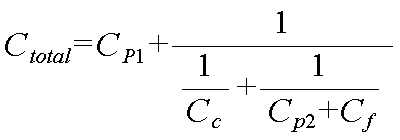
상기 <수학식 1> 및 <수학식 2>를 참조하면, 사용자가 복수의 센싱 패드들이 각각 회로에 연결되어 있지 않더라도 정전 용량의 변화량에 따라 어느 센싱 패드에서 터치가 발생하였는지를 판단할 수 있다. 이하, 보다 구체적인 실시 예를 설명하기로 한다.Referring to <Equation 1> and <Equation 2>, the user can determine which sensing pad has been touched based on the change in capacitance even if the plurality of sensing pads are not connected to the circuit. Hereinafter, a more specific embodiment will be described.
예컨대, 상기 <수학식 1> 및 <수학식 2>를 이용하여, 각 기생 정전 용량에 대해 특정 값을 삽입함으로써 주 센싱 패드와 부 센싱 패드 간의 상관관계를 분석할 수 있다. 후술하는 실시 예에서 주 센싱 패드와 손가락에 의한 기생 정전 용량은 각각 Cp1=155, Cf=3 의 고정 값을 사용하기로 한다. 나머지 Cp2와 Cc 값을 조절하여 하기 <표 5>와 같이 상관관계를 설명할 수 있다.For example, a correlation between the main sensing pad and the sub sensing pad may be analyzed by inserting a specific value for each parasitic capacitance using Equation 1 and Equation 2 above. In an embodiment to be described later, fixed values of C p1 =155 and C f =3 are used for the parasitic capacitance caused by the main sensing pad and the finger, respectively. The correlation can be explained as shown in Table 5 below by adjusting the remaining C p2 and C c values.
Cap.(pF)Total
Cap.(pF)
(limit=0.2)Detectable
(limit=0.2)
상기 <표 5>에서 delta=|Default-Total Cap| 값이 정전 센서의 잡음 레벨(noise level) (limit=0.2pF) 보다 높을 경우 터치 또는 그립 여부를 인식할 수 있다. 따라서, 상기 <표 5>의 Cf=CP2=Cc 상태에서는 각 센싱 패드의 터치 또는 그립 여부에 대한 식별이 가능하다.In <Table 5> above, delta=|Default-Total Cap| If the value is higher than the noise level (limit=0.2pF) of the capacitive sensor, whether the touch or grip can be recognized. Therefore, in the state of C f =C P2 =C c in Table 5, it is possible to identify whether each sensing pad has been touched or gripped.
하기 <표 6>은 다른 조건에서의 터치 또는 그립 감지 결과를 설명한다.Table 6 below describes touch or grip detection results under different conditions.
Cap.(pF)Total
Cap.(pF)
(limit=0.2)Detectable
(limit=0.2)
If. C f ≤ C P2
상기 <표 6>에서의 계산식을 통한 센싱 패드의 설계 조건 하기 <수학식 3>과 같이 설정될 수 있다.The design condition of the sensing pad through the calculation formula in <Table 6> can be set as shown in <Equation 3> below.

상기 <수학식 3>을 참조하면, Cf≤Cc 를 위해 주 센싱 패드와 부 센싱 패드의 간격을 커플링 발생 가능 거리 내에서 근접하도록 설계하고, Cf≥CP2 를 위해 부 센싱 패드의 평면적을 주 센싱 패드에 비해 상대적으로 작은 선 형태로 설계할 수 있다.Referring to Equation 3 above, for C f ≤ C c , the distance between the main sensing pad and the sub sensing pad is designed to be close within a coupling possible distance, and for C f ≥ C P2 , the distance between the main sensing pad and the sub sensing pad is The plane area can be designed in a relatively small line shape compared to the main sensing pad.
도 23은 본 발명의 다양한 실시 예에 따른 웨어러블 장치에서의 센싱 패드 설계 구조를 나타내는 도면이다. 도 23을 참조하면, 웨어러블 장치 내에서 주 센싱 패드(2311a) 및 복수의 부 센싱 패드들(2311b, 2311c)을 원형으로 구성할 수 있다.23 is a diagram illustrating a design structure of a sensing pad in a wearable device according to various embodiments of the present disclosure. Referring to FIG. 23 , a
상기 주 센싱 패드(2311a)는 정전 센서(2320)와 연결될 수 있으며, 다른 부 센싱 패드들(2311b, 2311c)과는 미리 설정된 거리만큼 이격되어 배치될 수 있다. 도시된 바와 같이 센싱 패드들이 이격되어 배치됨에 따라 상기 각 센싱 패드들 사이에는 커플링 정전 용량(2312a, 2312b, 2312c)이 생성될 수 있다.The
상기 주 센싱 패드(2311a)의 정전 용량(Cp1), 부 센싱 패드들(2311b, 2311c)의 정전 용량(Cp2, Cp3), 각 센싱 패드들 사이의 커플링 정전 용량(Cc1, Cc2, Cc3)은 하기 <수학식 4> 및 <수학식 5>와 같은 조건을 만족하도록 구성될 수 있다.The capacitance (C p1 ) of the

상기 <수학식 4>의 조건을 만족하는 경우, 터치 입력의 위치를 판단하기 위해 각 센싱 패드 간에는 하기 <수학식 5>와 같은 차등 조건이 추가될 수 있다.When the condition of <Equation 4> is satisfied, a differential condition as shown in <Equation 5> below may be added between each sensing pad to determine the location of a touch input.
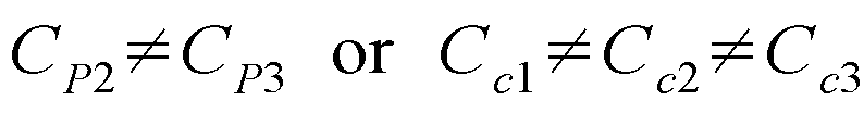
도 24는 본 발명의 다양한 실시 예에 따른 전자 장치에서의 터치 판단 절차를 나타내는 흐름도이다. 도 24를 참조하면, 동작 2402에서 프로세서를 통해 전자 장치의 상태 변화를 감지할 수 있다. 본 발명의 다양한 실시 예에 따라 상기 전자 장치의 상태 변화에 대응하여 프로세서를 통해 스위치를 온 또는 오프 상태로 제어할 수 있다.24 is a flowchart illustrating a touch determination procedure in an electronic device according to various embodiments of the present disclosure. Referring to FIG. 24 , in
예컨대, 동작 2404에서 상기 전자 장치가 비활성 상태이면, 동작 2406에서 상기 프로세서는 스위치를 오프 상태로 제어할 수 있다. 동작 2408에서 정전 센서를 구동시키면, 동작 2410에서 내부 정전 용량을 감지할 수 있다.For example, if the electronic device is in an inactive state in
동작 2412에서 상기 감지된 내부 정전 용량에 기반하여 오프셋 값을 저장함으로써 정전 센서에 대한 캘리브레이션을 수행할 수 있다.In
상기 동작 2404에서 전자 장치가 비활성 상태가 아니면, 동작 2414에서 스위치를 온 상태로 제어하고, 동작 2416에서는 정전 용량의 차이를 판단함으로써 터치 여부를 판단할 수 있다. If the electronic device is not in an inactive state in
전술한 바와 같이 본 발명의 다양한 실시 예에서는, 스위칭 회로를 제어함으로써 정전 센서를 통해 내부 정전 용량 및 외부 정전 용량을 측정할 수 있다. 본 발명의 다양한 실시 예에 따라 상기 내부 정전 용량 및 외부 정전 용량의 측정 결과에 대응하여 미리 설정된 특정 기능을 실행할 수 있다. 상기 기능은 전술한 바와 같이 터치 판단의 기준이 되는 오프셋 및 임계값을 업데이트하는 기능을 포함할 수 있으며, 내부 정전 용량 및 외부 정전 용량의 차이를 계산하고 사용자의 터치 또는 그립 여부를 판단하는 기능을 포함할 수 있다.As described above, in various embodiments of the present disclosure, internal capacitance and external capacitance may be measured through an electrostatic sensor by controlling a switching circuit. According to various embodiments of the present disclosure, a predetermined specific function may be executed in response to the measurement result of the internal capacitance and the external capacitance. As described above, the function may include a function of updating an offset and a threshold value that are criteria for determining a touch, and a function of calculating a difference between internal capacitance and external capacitance and determining whether a user touches or grips. can include
도 25는 본 발명의 다양한 실시 예에 따른 전자 장치에서의 터치 판단 절차를 나타내는 흐름도이다. 도 25를 참조하면, 동작 2502에서 전자 장치의 상태를 확인한다. 동작 2504에서 전자 장치의 상태가 슬립 이벤트로 판단되는 경우, 동작 2506에서 스위치를 오프 상태로 제어할 수 있다. 상기 스위치가 오프 상태로 됨에 따라 동작 2508에서 내부 정전 용량을 측정하고, 동작 2510에서 오프셋 및 임계값을 업데이트할 수 있다.25 is a flowchart illustrating a touch determination procedure in an electronic device according to various embodiments of the present disclosure. Referring to FIG. 25 , in
동작 2512에서 전자 장치가 비활성화되고, 동작 2514에서 웨이크업 이벤트가 발생하면, 동작 2516에서 다시 전자 장치를 활성화시킬 수 있다.If the electronic device is deactivated in
상기 동작 2504에서 슬립 이벤트가 아니거나, 상기 동작 2514에서 웨이크업 이벤트가 발생한 경우, 동작 2516에서 전자 장치는 활성화되고, 동작 2518에서 스위치를 온 상태로 제어할 수 있다. 동작 2520에서 정전 용량의 차이를 계산하고, 상기 계산된 정전 용량의 차이에 기반하여 동작 2522에서 터치 또는 그립 여부를 판단할 수 있다.If there is no sleep event in
이하, 도 26 및 도 27을 참조하여, 전자 장치 또는 웨어러블 장치의 구현 예를 설명한다.Hereinafter, implementation examples of an electronic device or a wearable device will be described with reference to FIGS. 26 and 27 .
도 26은 다양한 실시 예에 따른 전자 장치(2601)의 블록도(2600)이다. 상기 전자 장치(2601)는, 예를 들면, 도 5 내지 도 9에 도시된 전자 장치의 전체 또는 일부를 포함할 수 있다. 상기 전자 장치(2601)는 하나 이상의 애플리케이션 프로세서(AP: application processor)(2610), 통신 모듈(2620), SIM(subscriber identification module) 카드(2624), 메모리(2630), 센서 모듈(2640), 입력 장치(2650), 디스플레이(2660), 인터페이스(2670), 오디오 모듈(2680), 카메라 모듈(2691), 전력 관리 모듈(2695), 배터리(2696), 인디케이터(2697), 및 모터(2698)를 포함할 수 있다.26 is a block diagram 2600 of an electronic device 2601 according to various embodiments. The electronic device 2601 may include all or part of the electronic devices shown in FIGS. 5 to 9 , for example. The electronic device 2601 includes one or more application processors (APs) 2610, a
상기 AP(2610)는, 예를 들면, 운영 체제 또는 응용 프로그램을 구동하여 상기 AP(2610)에 연결된 다수의 하드웨어 또는 소프트웨어 구성요소들을 제어할 수 있고, 각종 데이터 처리 및 연산을 수행할 수 있다. 상기 AP(2610)는, 예를 들면, SoC(system on chip)로 구현될 수 있다. 한 실시 예에 따르면, 상기 AP(2610)는 GPU(graphic processing unit) 및/또는 이미지 신호 프로세서(image signal processor)를 더 포함할 수 있다. 상기 AP(2610)는 도 26에 도시된 구성요소들 중 적어도 일부(예: 셀룰러 모듈(2621))를 포함할 수도 있다. 상기 AP(2610)는 다른 구성요소들(예: 비휘발성 메모리) 중 적어도 하나로부터 수신된 명령 또는 데이터를 휘발성 메모리에 로드(load)하여 처리하고, 다양한 데이터를 비휘발성 메모리에 저장(store)할 수 있다.The
상기 통신 모듈(2620)은, 통신 인터페이스와 동일 또는 유사한 구성을 가질 수 있다. 상기 통신 모듈(2620)은, 예를 들면, 셀룰러 모듈(2621), WIFI 모듈(2623), BT 모듈(2625), GPS 모듈(2627), NFC 모듈(2628) 및 RF(radio frequency) 모듈(2629)을 포함할 수 있다.The
상기 셀룰러 모듈(2621)은, 예를 들면, 통신망을 통해서 음성 통화, 영상 통화, 문자 서비스, 또는 인터넷 서비스 등을 제공할 수 있다. 한 실시 예에 따르면, 상기 셀룰러 모듈(2621)은 가입자 식별 모듈(예: SIM 카드(2624))을 이용하여 통신 네트워크 내에서 전자 장치(2601)의 구별 및 인증을 수행할 수 있다. 한 실시 예에 따르면, 상기 셀룰러 모듈(2621)은 상기 AP(2610)가 제공할 수 있는 기능 중 적어도 일부 기능을 수행할 수 있다. 한 실시 예에 따르면, 상기 셀룰러 모듈(2621)은 커뮤니케이션 프로세서(CP: communication processor)를 포함할 수 있다.The
상기 WIFI 모듈(2623), 상기 BT 모듈(2625), 상기 GPS 모듈(2627) 또는 상기 NFC 모듈(2628) 각각은, 예를 들면, 해당하는 모듈을 통해서 송수신되는 데이터를 처리하기 위한 프로세서를 포함할 수 있다. 어떤 실시 예에 따르면, 셀룰러 모듈(2621), WIFI 모듈(2623), BT 모듈(2625), GPS 모듈(2627) 또는 NFC 모듈(2628) 중 적어도 일부(예: 두 개 이상)는 하나의 집적 칩(integrated chip)(IC) 또는 IC 패키지 내에 포함될 수 있다.Each of the
상기 RF 모듈(2629)은, 예를 들면, 통신 신호(예: RF 신호)를 송수신할 수 있다. 상기 RF 모듈(2629)은, 예를 들면, 트랜시버(transceiver), PAM(power amp module), 주파수 필터(frequency filter), LNA(low noise amplifier), 또는 안테나 등을 포함할 수 있다. 다른 실시 예에 따르면, 셀룰러 모듈(2621), WIFI 모듈(2623), BT 모듈(2625), GPS 모듈(2627) 또는 NFC 모듈(2628) 중 적어도 하나는 별개의 RF 모듈을 통하여 RF 신호를 송수신할 수 있다.The
상기 SIM 카드(2624)는, 예를 들면, 가입자 식별 모듈을 포함하는 카드 및/또는 내장 SIM(embedded SIM)을 포함할 수 있으며, 고유한 식별 정보(예: ICCID (integrated circuit card identifier)) 또는 가입자 정보(예: IMSI (international mobile subscriber identity))를 포함할 수 있다. The
상기 메모리(2630)는, 예를 들면, 내장 메모리(2632) 또는 외장 메모리(2634)를 포함할 수 있다. 상기 내장 메모리(2632)는, 예를 들면, 휘발성 메모리(예: DRAM(dynamic RAM), SRAM(static RAM), 또는 SDRAM(synchronous dynamic RAM) 등), 비휘발성 메모리(non-volatile Memory)(예: OTPROM(one time programmable ROM), PROM(programmable ROM), EPROM(erasable and programmable ROM), EEPROM(electrically erasable and programmable ROM), mask ROM, flash ROM, 플래시 메모리(예: NAND flash 또는 NOR flash 등), 하드 드라이브, 또는 솔리드 스테이트 드라이브(solid state drive (SSD)) 중 적어도 하나를 포함할 수 있다.The
상기 외장 메모리(2634)는 플래시 드라이브(flash drive), 예를 들면, CF(compact flash), SD(secure digital), Micro-SD(micro secure digital), Mini-SD(mini secure digital), xD(extreme digital), 또는 메모리 스틱(memory stick) 등을 더 포함할 수 있다. 상기 외장 메모리(2634)는 다양한 인터페이스를 통하여 상기 전자 장치(2601)와 기능적으로 및/또는 물리적으로 연결될 수 있다.The
상기 센서 모듈(2640)은, 예를 들면, 물리량을 계측하거나 전자 장치(2601)의 작동 상태를 감지하여, 계측 또는 감지된 정보를 전기 신호로 변환할 수 있다. 상기 센서 모듈(2640)은, 예를 들면, 제스처 센서(2640A), 자이로 센서(2640B), 기압 센서(2640C), 마그네틱 센서(2640D), 가속도 센서(2640E), 그립 센서(2640F), 근접 센서(2640G), 컬러(color) 센서(예: RGB(red, green, blue) 센서(2640H)), 생체 센서(2640I), 온/습도 센서(2640J), 조도 센서(2640K), 또는 UV(ultra violet) 센서(2640M) 중의 적어도 하나를 포함할 수 있다. 추가적으로 또는 대안적으로, 상기 센서 모듈(2640)은, 예를 들면, 후각 센서(E-nose sensor), EMG 센서(electromyography sensor), EEG 센서(electroencephalogram sensor), ECG 센서(electrocardiogram sensor), IR(infrared) 센서, 홍채 센서 및/또는 지문 센서를 포함할 수 있다. 상기 센서 모듈(2640)은 그 안에 속한 적어도 하나 이상의 센서들을 제어하기 위한 제어 회로를 더 포함할 수 있다. 어떤 실시 예에서는, 전자 장치(2601)는 AP(2610)의 일부로서 또는 별도로, 센서 모듈(2640)을 제어하도록 구성된 프로세서를 더 포함하여, 상기 AP(2610)가 슬립 (sleep) 상태에 있는 동안, 센서 모듈(2640)을 제어할 수 있다.The
상기 입력 장치(2650)는, 예를 들면, 터치 패널 (touch panel)(2652), (디지털) 펜 센서(pen sensor)(2654), 키 (key)(2656), 또는 초음파(ultrasonic) 입력 장치(2658)를 포함할 수 있다. 상기 터치 패널(2652)은, 예를 들면, 정전식, 감압식, 적외선 방식, 또는 초음파 방식 중 적어도 하나의 방식을 사용할 수 있다. 또한, 상기 터치 패널(2652)은 제어 회로를 더 포함할 수도 있다. 상기 터치 패널(2652)은 택타일 레이어(tactile layer)를 더 포함하여, 사용자에게 촉각 반응을 제공할 수 있다.The
상기 (디지털) 펜 센서(2654)는, 예를 들면, 터치 패널의 일부이거나, 별도의 인식용 쉬트(sheet)를 포함할 수 있다. 상기 키(2656)는, 예를 들면, 물리적인 버튼, 광학식 키, 또는 키패드를 포함할 수 있다. 상기 초음파 입력 장치(2658)는 초음파 신호를 발생하는 입력 도구를 통해, 전자 장치(2601)에서 마이크(예: 마이크(2688))로 음파를 감지하여 데이터를 확인할 수 있다.The (digital)
상기 디스플레이(2660)(예: 디스플레이(160))는 패널(2662), 홀로그램 장치(2664), 또는 프로젝터(2666)를 포함할 수 있다. 상기 패널(2662)은, 예를 들면, 유연하게 (flexible), 투명하게 (transparent), 또는 착용할 수 있게 (wearable) 구현될 수 있다. 상기 패널(2662)은 상기 터치 패널(2652)과 하나의 모듈로 구성될 수도 있다. 상기 홀로그램 장치(2664)는 빛의 간섭을 이용하여 입체 영상을 허공에 보여줄 수 있다. 상기 프로젝터(2666)는 스크린에 빛을 투사하여 영상을 표시할 수 있다. 상기 스크린은, 예를 들면, 상기 전자 장치(2601)의 내부 또는 외부에 위치할 수 있다. 한 실시 예에 따르면, 상기 디스플레이(2660)는 상기 패널(2662), 상기 홀로그램 장치(2664), 또는 프로젝터(2666)를 제어하기 위한 제어 회로를 더 포함할 수 있다.The display 2660 (eg, the display 160) may include a
상기 인터페이스(2670)는, 예를 들면, HDMI(high-definition multimedia interface)(2672), USB(universal serial bus)(2674), 광 인터페이스(optical interface)(2676), 또는 D-sub(D-subminiature)(2678)를 포함할 수 있다. 상기 인터페이스(2670)는 예를 들면, MHL(mobile high-definition link) 인터페이스, SD(secure digital) 카드/MMC(multi-media card) 인터페이스, 또는 IrDA(infrared data association) 규격 인터페이스를 포함할 수 있다.The
상기 오디오 모듈(2680)은, 예를 들면, 소리(sound)와 전기 신호를 쌍방향으로 변환시킬 수 있다. 상기 오디오 모듈(2680)의 적어도 일부 구성요소는, 예를 들면, 스피커(2682), 리시버(2684), 이어폰(2686), 또는 마이크(2688) 등을 통해 입력 또는 출력되는 소리 정보를 처리할 수 있다.The
상기 카메라 모듈(2691)은, 예를 들면, 정지 영상 및 동영상을 촬영할 수 있는 장치로서, 한 실시 예에 따르면, 하나 이상의 이미지 센서(예: 전면 센서 또는 후면 센서), 렌즈, ISP(image signal processor), 또는 플래쉬(flash)(예: LED 또는 xenon lamp)를 포함할 수 있다.The
상기 전력 관리 모듈(2695)은, 예를 들면, 상기 전자 장치(2601)의 전력을 관리할 수 있다. 한 실시 예에 따르면, 상기 전력 관리 모듈(2695)은 PMIC(power management integrated circuit), 충전 IC(charger integrated circuit), 또는 배터리 또는 연료 게이지(battery or fuel gauge)를 포함할 수 있다. 상기 PMIC는, 유선 및/또는 무선 충전 방식을 가질 수 있다. 무선 충전 방식은, 예를 들면, 자기공명 방식, 자기유도 방식 또는 전자기파 방식 등을 포함하며, 무선 충전을 위한 부가적인 회로, 예를 들면, 코일 루프, 공진 회로, 또는 정류기 등을 더 포함할 수 있다. 상기 배터리 게이지는, 예를 들면, 상기 배터리(2696)의 잔량, 충전 중 전압, 전류, 또는 온도를 측정할 수 있다. 상기 배터리(2696)는, 예를 들면, 충전식 전지(rechargeable battery) 및/또는 태양 전지(solar battery)를 포함할 수 있다.The
상기 인디케이터(2697)는 상기 전자 장치(2601) 혹은 그 일부(예: AP(2610))의 특정 상태, 예를 들면, 부팅 상태, 메시지 상태 또는 충전 상태 등을 표시할 수 있다. 상기 모터(2698)는 전기적 신호를 기계적 진동으로 변환할 수 있고, 진동(vibration), 또는 햅틱(haptic) 효과 등을 발생시킬 수 있다. 도시되지는 않았으나, 상기 전자 장치(2601)는 모바일 TV 지원을 위한 처리 장치(예: GPU)를 포함할 수 있다. 상기 모바일 TV 지원을 위한 처리 장치는, 예를 들면, DMB(digital multimedia broadcasting), DVB(digital video broadcasting), 또는 미디어 플로우 (media flow) 등의 규격에 따른 미디어 데이터를 처리할 수 있다.The
상기 전자 장치의 전술한 구성요소들 각각은 하나 또는 그 이상의 부품 (component)으로 구성될 수 있으며, 해당 구성 요소의 명칭은 전자 장치의 종류에 따라서 달라질 수 있다. 다양한 실시 예에서, 전자 장치는 전술한 구성요소 중 적어도 하나를 포함하여 구성될 수 있으며, 일부 구성요소가 생략되거나 또는 추가적인 다른 구성요소를 더 포함할 수 있다. 또한, 다양한 실시 예에 따른 전자 장치의 구성 요소들 중 일부가 결합되어 하나의 개체(entity)로 구성됨으로써, 결합되기 이전의 해당 구성 요소들의 기능을 동일하게 수행할 수 있다.Each of the aforementioned components of the electronic device may be composed of one or more components, and the name of the corresponding component may vary depending on the type of electronic device. In various embodiments, an electronic device may include at least one of the above-described components, and some components may be omitted or additional components may be further included. In addition, some of the components of the electronic device according to various embodiments are combined to form one entity, so that the functions of the corresponding components before being combined can be performed the same.
도 27은 다양한 실시 예에 따른 프로그램 모듈(2710)의 블록도(2700)이다. 한 실시 예에 따르면, 상기 프로그램 모듈(2710)은 전자 장치(예: 도 5 내지 도 9의 전자 장치)에 관련된 자원을 제어하는 운영 체제(operation system (OS)) 및/또는 운영 체제상에서 구동되는 다양한 애플리케이션을 포함할 수 있다. 상기 운영 체제는, 예를 들면, 안드로이드(android), iOS, 윈도우즈(windows), 심비안(symbian), 타이젠(tizen), 또는 바다(bada) 등이 될 수 있다.27 is a block diagram 2700 of a
프로그램 모듈(2710)은 커널(2720), 미들웨어(2730), API(application programming interface)(2760), 및/또는 애플리케이션(2770)을 포함할 수 있다. 상기 프로그램 모듈(2710)의 적어도 일부는 전자 장치상에 프리로드(preload) 되거나, 서버(예: 서버(106))로부터 다운로드(download) 가능하다.The
상기 커널(2720)은, 예를 들면, 시스템 리소스 매니저(2721) 또는 디바이스 드라이버(2723)를 포함할 수 있다. 상기 시스템 리소스 매니저(2721)는 시스템 리소스의 제어, 할당, 또는 회수 등을 수행할 수 있다. 한 실시 예에 따르면, 상기 시스템 리소스 매니저(2721)는 프로세스 관리부, 메모리 관리부, 또는 파일 시스템 관리부 등을 포함할 수 있다. 상기 디바이스 드라이버(2723)는, 예를 들면, 디스플레이 드라이버, 카메라 드라이버, 블루투스 드라이버, 공유 메모리 드라이버, USB 드라이버, 키패드 드라이버, WIFI 드라이버, 오디오 드라이버, 또는 IPC(inter-process communication) 드라이버를 포함할 수 있다. The
상기 미들웨어(2730)는, 예를 들면, 상기 애플리케이션(2770)이 공통적으로 필요로 하는 기능을 제공하거나, 상기 애플리케이션(2770)이 전자 장치 내부의 제한된 시스템 자원을 효율적으로 사용할 수 있도록 상기 API(2760)를 통해 다양한 기능들을 상기 애플리케이션(2770)으로 제공할 수 있다. 한 실시 예에 따르면, 상기 미들웨어(2730)(예: 미들웨어 (143))는 런타임 라이브러리(2735), 애플리케이션 매니저(application manager)(2741), 윈도우 매니저(window manager)(2742), 멀티미디어 매니저(multimedia manager)(2743), 리소스 매니저(resource manager)(2744), 파워 매니저(power manager)(2745), 데이터베이스 매니저(database manager)(2746), 패키지 매니저(package manager)(2747), 연결 매니저(connectivity manager)(2748), 통지 매니저(notification manager)(2749), 위치 매니저 (location manager)(2750), 그래픽 매니저(graphic manager)(2751), 또는 보안 매니저(security manager)(2752) 중 적어도 하나를 포함할 수 있다.The
상기 런타임 라이브러리(2735)는, 예를 들면, 상기 애플리케이션(2770)이 실행되는 동안에 프로그래밍 언어를 통해 새로운 기능을 추가하기 위해 컴파일러가 사용하는 라이브러리 모듈을 포함할 수 있다. 상기 런타임 라이브러리(2735)는 입출력 관리, 메모리 관리, 또는 산술 함수에 대한 기능 등을 수행할 수 있다.The
상기 애플리케이션 매니저(2741)는, 예를 들면, 상기 애플리케이션(2770) 중 적어도 하나의 애플리케이션의 라이프 사이클(life cycle)을 관리할 수 있다. 상기 윈도우 매니저(2742)는 화면에서 사용하는 GUI 자원을 관리할 수 있다. 상기 멀티미디어 매니저(2743)는 다양한 미디어 파일들의 재생에 필요한 포맷을 파악하고, 해당 포맷에 맞는 코덱(codec)을 이용하여 미디어 파일의 인코딩(encoding) 또는 디코딩(decoding)을 수행할 수 있다. 상기 리소스 매니저(2744)는 상기 애플리케이션(2770) 중 적어도 어느 하나의 애플리케이션의 소스 코드, 메모리 또는 저장 공간 등의 자원을 관리할 수 있다.The
상기 파워 매니저(2745)는, 예를 들면, 바이오스(BIOS: basic input/output system) 등과 함께 동작하여 배터리(battery) 또는 전원을 관리하고, 전자 장치의 동작에 필요한 전력 정보 등을 제공할 수 있다. 상기 데이터베이스 매니저(2746)는 상기 애플리케이션(2770) 중 적어도 하나의 애플리케이션에서 사용할 데이터베이스를 생성, 검색, 또는 변경할 수 있다. 상기 패키지 매니저(2747)는 패키지 파일의 형태로 배포되는 애플리케이션의 설치 또는 업데이트를 관리할 수 있다.The
상기 연결 매니저(2748)는, 예를 들면, WIFI 또는 블루투스 등의 무선 연결을 관리할 수 있다. 상기 통지 매니저(2749)는 도착 메시지, 약속, 근접성 알림 등의 사건 (event)을 사용자에게 방해되지 않는 방식으로 표시 또는 통지할 수 있다. 상기 위치 매니저(2750)는 전자 장치의 위치 정보를 관리할 수 있다. 상기 그래픽 매니저(2751)는 사용자에게 제공될 그래픽 효과 또는 이와 관련된 사용자 인터페이스를 관리할 수 있다. 상기 보안 매니저(2752)는 시스템 보안 또는 사용자 인증 등에 필요한 제반 보안 기능을 제공할 수 있다. 한 실시 예에 따르면, 전자 장치가 전화 기능을 포함한 경우, 상기 미들웨어(2730)는 상기 전자 장치의 음성 또는 영상 통화 기능을 관리하기 위한 통화 매니저(telephony manager)를 더 포함할 수 있다.The
상기 미들웨어(2730)는 전술한 구성요소들의 다양한 기능의 조합을 형성하는 미들웨어 모듈을 포함할 수 있다. 상기 미들웨어(2730)는 차별화된 기능을 제공하기 위해 운영 체제의 종류별로 특화된 모듈을 제공할 수 있다. 또한, 상기 미들웨어(2730)는 동적으로 기존의 구성요소를 일부 삭제하거나 새로운 구성요소들을 추가할 수 있다.The
상기 API(2760)는, 예를 들면, API 프로그래밍 함수들의 집합으로, 운영 체제에 따라 다른 구성으로 제공될 수 있다. 예를 들면, 안드로이드 또는 iOS의 경우, 플랫폼별로 하나의 API 셋을 제공할 수 있으며, 타이젠(tizen)의 경우, 플랫폼별로 두 개 이상의 API 셋을 제공할 수 있다.The
상기 애플리케이션(2770)은, 예를 들면, 홈(2771), 다이얼러(2772), SMS/MMS(2773), IM(instant message)(2774), 브라우저(2775), 카메라(2776), 알람(2777), 컨택트(2778), 음성 다이얼(2779), 이메일(2780), 달력(2781), 미디어 플레이어(2782), 앨범(2783), 또는 시계(2784), 건강 관리(health care)(예: 운동량 또는 혈당 등을 측정), 또는 환경 정보 제공(예: 기압, 습도, 또는 온도 정보 등을 제공) 등의 기능을 제공할 수 있는 하나 이상의 애플리케이션을 포함할 수 있다.The
한 실시 예에 따르면, 상기 애플리케이션(2770)은 상기 전자 장치와 외부 전자 장치 사이의 정보 교환을 지원하는 애플리케이션(이하, 설명의 편의 상, "정보 교환 애플리케이션")을 포함할 수 있다. 상기 정보 교환 애플리케이션은, 예를 들면, 상기 외부 전자 장치에 특정 정보를 전달하기 위한 알림 전달(notification relay) 애플리케이션, 또는 상기 외부 전자 장치를 관리하기 위한 장치 관리(device management) 애플리케이션을 포함할 수 있다.According to one embodiment, the
예를 들면, 상기 알림 전달 애플리케이션은 상기 전자 장치의 다른 애플리케이션(예: SMS/MMS 애플리케이션, 이메일 애플리케이션, 건강 관리 애플리케이션, 또는 환경 정보 애플리케이션 등)에서 발생된 알림 정보를 외부 전자 장치로 전달하는 기능을 포함할 수 있다. 또한, 상기 알림 전달 애플리케이션은, 예를 들면, 외부 전자 장치로부터 알림 정보를 수신하여 사용자에게 제공할 수 있다. 상기 장치 관리 애플리케이션은, 예를 들면, 상기 전자 장치와 통신하는 외부 전자 장치의 적어도 하나의 기능(예: 외부 전자 장치 자체(또는, 일부 구성 부품)의 턴-온/턴-오프 또는 디스플레이의 밝기(또는, 해상도) 조절), 상기 외부 전자 장치에서 동작하는 애플리케이션 또는 상기 외부 전자 장치에서 제공되는 서비스(예: 통화 서비스 또는 메시지 서비스)를 관리(예: 설치, 삭제, 또는 업데이트)할 수 있다.For example, the notification delivery application functions to deliver notification information generated from other applications (eg, an SMS/MMS application, an email application, a health management application, or an environment information application) of the electronic device to an external electronic device. can include Also, the notification delivery application may receive notification information from an external electronic device and provide the notification information to the user. The device management application may, for example, perform at least one function of an external electronic device communicating with the electronic device (eg, turn-on/turn-off of the external electronic device itself (or some components) or brightness of a display). (or resolution), management (eg, installation, deletion, or update) of an application operating in the external electronic device or a service (eg, call service or message service) provided by the external electronic device.
한 실시 예에 따르면, 상기 애플리케이션(2770)은 상기 외부 전자 장치의 속성(예: 전자 장치의 속성으로서, 전자 장치의 종류가 모바일 의료 기기)에 따라 지정된 애플리케이션(예: 건강 관리 애플리케이션)을 포함할 수 있다. 한 실시 예에 따르면, 상기 애플리케이션(2770)은 외부 전자 장치로부터 수신된 애플리케이션을 포함할 수 있다. 한 실시 예에 따르면, 상기 애플리케이션(2770)은 프리로드 애플리케이션(preloaded application) 또는 서버로부터 다운로드 가능한 제3자 애플리케이션(third party application)을 포함할 수 있다. 도시된 실시 예에 따른 프로그램 모듈(2710)의 구성요소들의 명칭은 운영 체제의 종류에 따라서 달라질 수 있다.According to an embodiment, the
다양한 실시 예에 따르면, 상기 프로그램 모듈(2710)의 적어도 일부는 소프트웨어, 펌웨어, 하드웨어, 또는 이들 중 적어도 둘 이상의 조합으로 구현될 수 있다. 상기 프로그램 모듈(2710)의 적어도 일부는, 예를 들면, 프로세서(예: AP(2610))에 의해 구현(implement)(예: 실행)될 수 있다. 상기 프로그램 모듈(2710)의 적어도 일부는 하나 이상의 기능을 수행하기 위한, 예를 들면, 모듈, 프로그램, 루틴, 명령어 세트(sets of instructions) 또는 프로세스 등을 포함할 수 있다.According to various embodiments, at least a part of the
본 문서에서 사용된 용어 "모듈" 또는 "기능부"는, 예를 들면, 하드웨어, 소프트웨어 또는 펌웨어(firmware) 중 하나 또는 둘 이상의 조합을 포함하는 단위(unit)를 의미할 수 있다. "모듈" 또는 "기능부"는, 예를 들면, 유닛(unit), 로직(logic), 논리 블록(logical block), 부품(component), 또는 회로(circuit) 등의 용어와 바꾸어 사용(interchangeably use)될 수 있다. "모듈" 또는 "기능부"는, 일체로 구성된 부품의 최소 단위 또는 그 일부가 될 수 있다. "모듈"은 하나 또는 그 이상의 기능을 수행하는 최소 단위 또는 그 일부가 될 수도 있다. "모듈" 또는 "기능부"는 기계적으로 또는 전자적으로 구현될 수 있다. 예를 들면, "모듈" 또는 "기능부"는, 알려졌거나 앞으로 개발될, 어떤 동작들을 수행하는 ASIC(application-specific integrated circuit) 칩, FPGAs(field-programmable gate arrays) 또는 프로그램 가능 논리 장치(programmable-logic device) 중 적어도 하나를 포함할 수 있다.The term "module" or "functional unit" used in this document may refer to a unit including one or a combination of two or more of, for example, hardware, software, or firmware. "Module" or "functional unit" is used interchangeably with terms such as, for example, unit, logic, logical block, component, or circuit. ) can be A “module” or “functional unit” may be a minimum unit or part of an integrally formed part. A “module” may be a minimal unit or part thereof that performs one or more functions. A “module” or “functional unit” may be implemented mechanically or electronically. For example, a "module" or "functional unit" is a known or future developed application-specific integrated circuit (ASIC) chip, field-programmable gate arrays (FPGAs), or programmable logic device that performs certain operations. -logic device).
다양한 실시 예에 따른 장치(예: 모듈들 또는 그 기능들) 또는 방법(예: 동작들)의 적어도 일부는, 예컨대, 프로그램 모듈의 형태로 컴퓨터로 읽을 수 있는 저장매체(computer-readable storage media)에 저장된 명령어로 구현될 수 있다. 상기 명령어는, 프로세서 (예: 프로세서(560, 660, 770, 860, 950)에 의해 실행될 경우, 상기 하나 이상의 프로세서가 상기 명령어에 해당하는 기능을 수행할 수 있다. 컴퓨터로 읽을 수 있는 저장매체는, 예를 들면, 메모리가 될 수 있다.At least some of devices (eg, modules or functions thereof) or methods (eg, operations) according to various embodiments of the present disclosure are, for example, computer-readable storage media in the form of program modules. It can be implemented as a command stored in . When the instruction is executed by a processor (eg, the
상기 컴퓨터로 판독 가능한 기록 매체는, 하드디스크, 플로피디스크, 마그네틱 매체(magnetic media)(예: 자기테이프), 광기록 매체(optical media)(예: CD-ROM(compact disc read only memory), DVD(digital versatile disc), 자기-광 매체(magneto-optical media)(예: 플롭티컬 디스크(floptical disk)), 하드웨어 장치(예: ROM(read only memory), RAM(random access memory), 또는 플래시 메모리 등) 등을 포함할 수 있다. 또한, 프로그램 명령에는 컴파일러에 의해 만들어지는 것과 같은 기계어 코드뿐만 아니라 인터프리터 등을 사용해서 컴퓨터에 의해서 실행될 수 있는 고급 언어 코드를 포함할 수 있다. 상술한 하드웨어 장치는 다양한 실시 예의 동작을 수행하기 위해 하나 이상의 소프트웨어 모듈로서 작동하도록 구성될 수 있으며, 그 역도 마찬가지다.The computer-readable recording medium includes a hard disk, a floppy disk, magnetic media (eg, magnetic tape), optical media (eg, CD-ROM (compact disc read only memory), DVD (digital versatile disc), magneto-optical media (such as floptical disk), hardware devices (such as read only memory (ROM), random access memory (RAM), or flash memory) etc.), etc. In addition, program instructions may include not only machine code generated by a compiler, but also high-level language code that can be executed by a computer using an interpreter, etc. The above-described hardware device may include It may be configured to act as one or more software modules to perform the operations of various embodiments, and vice versa.
다양한 실시 예에 따른 모듈 또는 프로그램 모듈은 전술한 구성요소들 중 적어도 하나 이상을 포함하거나, 일부가 생략되거나, 또는 추가적인 다른 구성요소를 더 포함할 수 있다. 다양한 실시 예에 따른 모듈, 프로그램 모듈 또는 다른 구성요소에 의해 수행되는 동작들은 순차적, 병렬적, 반복적 또는 휴리스틱(heuristic)한 방법으로 실행될 수 있다. 또한, 일부 동작은 다른 순서로 실행되거나, 생략되거나, 또는 다른 동작이 추가될 수 있다.A module or program module according to various embodiments may include at least one or more of the aforementioned components, some may be omitted, or additional components may be further included. Operations performed by modules, program modules, or other components according to various embodiments may be executed in a sequential, parallel, repetitive, or heuristic manner. Also, some actions may be performed in a different order, omitted, or other actions may be added.
그리고 본 명세서와 도면에 발명된 본 발명의 실시 예들은 본 발명의 실시 예에 따른 기술 내용을 쉽게 설명하고 본 발명의 실시 예의 이해를 돕기 위해 특정 예를 제시한 것일 뿐이며, 본 발명의 실시 예의 범위를 한정하고자 하는 것은 아니다. 따라서 본 발명의 다양한 실시 예의 범위는 여기에 발명된 실시 예들 이외에도 본 발명의 다양한 실시 예의 기술적 사상을 바탕으로 도출되는 모든 변경 또는 변형된 형태가 본 발명의 다양한 실시 예의 범위에 포함되는 것으로 해석되어야 한다.In addition, the embodiments of the present invention described in the present specification and drawings are only presented as specific examples to easily explain the technical content according to the embodiments of the present invention and help understanding of the embodiments of the present invention, and the scope of the embodiments of the present invention is not intended to limit Therefore, the scope of various embodiments of the present invention should be construed as including all changes or modified forms derived based on the technical spirit of various embodiments of the present invention in addition to the embodiments disclosed herein are included in the scope of various embodiments of the present invention. .
101 : 기생 정전 용량 102 : 비교기
103 : 클록 카운터 200, 300 : 웨어러블 장치
210, 311, 312 : IR 센서 220, 321, 322: LED
410 : 터치 회로 420 , 430 : 센싱 패드
421, 431 : 센싱 채널 510 : 외부 정전 용량
511 : 센싱 패드부 511a : 주 센싱 패드
511b, 511c : 부 센싱 패드 512 : 연결 회로
520 : 스위칭 회로 530 : 내부 정전 용량
531 : 보호 회로 532 : 매칭 회로
533 : 보상 회로 540 : 무선 통신 회로
550 : 정전 센서 560 : 프로세서101: parasitic capacitance 102: comparator
103:
210, 311, 312:
410:
421, 431: sensing channel 510: external capacitance
511: sensing
511b, 511c: sub-sensing pad 512: connection circuit
520: switching circuit 530: internal capacitance
531: protection circuit 532: matching circuit
533: compensation circuit 540: wireless communication circuit
550: electrostatic sensor 560: processor
Claims (20)
제1 면, 상기 제1 면의 반대로 향하는 제2 면, 및 상기 제1 면 및 제2 면 사이의 공간을 적어도 일부 둘러싸는 측면을 포함하는 하우징;
상기 하우징의 내부에 배치된 무선 통신 회로;
상기 하우징의 제1 면, 제2 면, 및/또는 측면 중 적어도 하나의 적어도 일부를 형성하고, 상기 무선 통신 회로와 전기적으로 연결된 안테나 방사체;
상기 안테나 방사체의 적어도 일부를 형성하거나, 상기 안테나 방사체로부터 이격되어 배치된 제 1 도전성 부재;
상기 하우징의 내부에 배치된 스위칭 회로;
상기 제1 도전성 부재와 상기 스위칭 회로를 통하여 전기적으로 연결 가능하고, 상기 제1 도전성 부재에 대한 외부 물체의 접촉 또는 근접을 감지하도록 구성된 센서;
상기 무선 통신 회로, 상기 스위칭 회로, 및 상기 센서와 전기적으로 연결된 프로세서; 및
상기 프로세서와 전기적으로 연결된 메모리를 포함하고,
상기 메모리는, 실행시에, 상기 프로세서가,
상기 전자 장치의 적어도 일부가 활성화 되었는지 여부를 판단하고,
상기 스위칭 회로를 이용하여,
상기 전자 장치의 적어도 일부가 비활성화 된 경우, 상기 센서와 상기 제1 도전성 부재를 전기적으로 분리하는 제1 상태를 제공하고,
상기 전자 장치의 적어도 일부가 활성화된 경우, 상기 센서와 상기 제1 도전성 부재를 전기적으로 연결하는 제2 상태를 제공하도록 하는 인스트럭션들을 저장하는 것을 특징으로 하는 장치.In electronic devices,
a housing including a first surface, a second surface opposite to the first surface, and a side surface at least partially enclosing a space between the first surface and the second surface;
a wireless communication circuit disposed inside the housing;
an antenna radiator that forms at least a portion of at least one of the first, second, and/or side surfaces of the housing and is electrically connected to the wireless communication circuit;
a first conductive member that forms at least a part of the antenna radiator or is spaced apart from the antenna radiator;
a switching circuit disposed inside the housing;
a sensor electrically connectable to the first conductive member through the switching circuit and configured to detect a contact or proximity of an external object to the first conductive member;
a processor electrically connected to the wireless communication circuit, the switching circuit, and the sensor; and
A memory electrically connected to the processor;
The memory, when executed, the processor,
determining whether at least a part of the electronic device is activated;
Using the switching circuit,
providing a first state in which the sensor and the first conductive member are electrically separated when at least a part of the electronic device is inactivated;
and storing instructions to provide a second state electrically connecting the sensor and the first conductive member when at least a part of the electronic device is activated.
상기 제1 상태에서 제1 데이터를 획득하고,
상기 제2 상태에서 제2 데이터를 획득하며,
상기 제1 데이터 및 상기 제2 데이터에 적어도 일부 기초하여, 상기 제1 도전성 부재에 대한 사용자의 신체의 접촉 또는 근접 여부를 판단하도록 하는 것을 특징으로 하는 장치.The method of claim 1, wherein the instructions, the processor, using the sensor,
Obtaining first data in the first state;
Obtaining second data in the second state;
and determining whether a user's body is in contact with or approaching the first conductive member based at least in part on the first data and the second data.
상기 제1 데이터 및 상기 제2 데이터의 차이가 쓰레쉬홀드 값 미만인 경우, 상기 제1 도전성 부재로부터 상기 사용자의 신체가 이격되었다고 판단하고,
상기 제1 데이터 및 상기 제2 데이터의 차이가 상기 쓰레쉬홀드 값 이상인 경우, 상기 제1 도전성 부재에 상기 사용자의 신체가 접촉 또는 근접하다고 판단하도록 하는 것을 특징으로 하는 장치.The method of claim 2, wherein the instructions, the processor,
When a difference between the first data and the second data is less than a threshold value, it is determined that the user's body is separated from the first conductive member;
and when a difference between the first data and the second data is greater than or equal to the threshold value, it is determined that the user's body is in contact with or approaching the first conductive member.
상기 제1 데이터에 적어도 일부 기초하여, 상기 제2 데이터를 보정하고,
상기 보정된 제2 데이터에 적어도 일부 기초하여, 상기 제1 도전성 부재에 대한 사용자의 신체의 접촉 또는 근접 여부를 판단하며,
상기 전자 장치는,
상기 스위칭 회로 및 상기 센서 사이에 전기적으로 연결되고, 상기 제1 데이터를 적어도 일부 저장하도록 구성된 보상 회로를 더 포함하고,
상기 인스트럭션들은, 상기 프로세서가, 상기 보상 회로를 이용하여, 상기 제2 데이터를 보정하도록 하는 것을 특징으로 하는 장치.The method of claim 2, wherein the instructions, the processor,
Correcting the second data based at least in part on the first data;
Based at least in part on the corrected second data, determining whether or not the user's body is in contact or proximity to the first conductive member;
The electronic device,
a compensation circuit electrically coupled between the switching circuit and the sensor and configured to store at least a portion of the first data;
The instructions may cause the processor to correct the second data using the compensation circuit.
상기 제1 도전성 부재로부터 절연된 제2 도전성 부재를 더 포함하며,
상기 제1 도전성 부재 및 상기 제 2 도전성 부재 사이에 형성된 캐패시턴스 CC,
상기 제1 도전성 부재 및/또는 상기 제2 도전성 부재와, 사용자의 신체 사이에 형성된 캐패시턴스 Cf,
상기 제1 도전성 부재에서 형성된 기생 캐패시턴스 CP1, 및
상기 제2 도전성 부재에서 형성된 기생 캐패시턴스 CP2 는,
CP1> CP2, Cf≥CP2, 또는 Cf≤Cc 중 적어도 하나의 관계를 만족하는 것을 특징으로 하는 장치.The method of claim 1, wherein the electronic device,
Further comprising a second conductive member insulated from the first conductive member,
A capacitance C C formed between the first conductive member and the second conductive member,
A capacitance C f formed between the first conductive member and/or the second conductive member and the user's body;
A parasitic capacitance C P1 formed in the first conductive member, and
The parasitic capacitance C P2 formed in the second conductive member is
C P1 > C P2 , C f ≥ C P2 , or C f ≤ C c The device characterized in that it satisfies at least one relationship.
상기 제1 도전성 부재로부터 절연된 제2 도전성 부재 및 상기 제2 도전성 부재로부터 절연된, 제3 도전성 부재를 더 포함하며,
상기 제1 도전성 부재 및 상기 제2 도전성 부재 사이에 형성된 캐패시턴스 CC1,
상기 제1 도전성 부재 및 상기 제3 도전성 부재 사이에 형성된 캐패시턴스 CC2,
상기 제2 도전성 부재 및 상기 제3 도전성 부재 사이에 형성된 캐패시턴스 CC3,
상기 제1 도전성 부재, 상기 제2 도전성 부재, 및/또는 상기 제3 도전성 부재와 사용자의 신체 사이에 형성된 캐패시턴스 Cf,
상기 제1 도전성 부재에서 형성된 기생 캐패시턴스 CP1,
상기 제2 도전성 부재에서 형성된 기생 캐패시턴스 CP2, 및
상기 제3 도전성 부재에서 형성된 기생 캐패시턴스 CP3 는,
CP1> CP2 or CP3, Cf≥CP2 or CP3, Cf≤Cc1 or CC2, CP2≠CP3, 또는 Cc1≠Cc2≠Cc3 중 적어도 하나의 관계를 만족하는 것을 특징으로 하는 장치.The method of claim 1, wherein the electronic device,
Further comprising a second conductive member insulated from the first conductive member and a third conductive member insulated from the second conductive member,
A capacitance C C1 formed between the first conductive member and the second conductive member;
A capacitance C C2 formed between the first conductive member and the third conductive member;
A capacitance C C3 formed between the second conductive member and the third conductive member;
A capacitance C f formed between the first conductive member, the second conductive member, and/or the third conductive member and the user's body;
Parasitic capacitance C P1 formed in the first conductive member;
A parasitic capacitance C P2 formed in the second conductive member, and
The parasitic capacitance C P3 formed in the third conductive member is
C P1 > C P2 or C P3 , C f ≥ C P2 or C P3 , C f ≤ C c1 or C C2 , C P2 ≠ C P3 , or C c1 ≠ C c2 ≠ C c3 device characterized in that
인쇄회로기판 및 상기 제1 도전성 부재 사이에 전기적으로 연결되고, 상기 안테나 방사체에 인가되어 상기 인쇄회로기판으로 유입되는 정전기를 적어도 일부 차단하도록 구성된 보호 회로를 더 포함하며,
상기 스위칭 회로는, 적어도 하나의 트랜지스터를 포함하고,
상기 적어도 하나의 트랜지스터에 인가된 적어도 하나의 신호에 기초하여 스위칭하도록 구성되며,
상기 센서는, 상기 센서로부터 발생되어, 상기 제1 도전성 부재를 통하여 돌아온 신호에 기초하여, 상기 제1 도전성 부재 및 외부 물체 사이에 형성된 정전용량의 변화를 검출하도록 구성된 것을 특징으로 하는 장치.The method of claim 1, wherein the electronic device,
A protective circuit electrically connected between the printed circuit board and the first conductive member and configured to block at least some static electricity applied to the antenna radiator and flowing into the printed circuit board,
The switching circuit includes at least one transistor,
configured to switch based on at least one signal applied to the at least one transistor;
wherein the sensor is configured to detect a change in capacitance formed between the first conductive member and an external object based on a signal generated from the sensor and returned through the first conductive member.
제1 면, 상기 제1 면의 반대로 향하는 제2 면, 및 상기 제1 면 및 제2 면 사이의 공간을 적어도 일부 둘러싸는 측면을 포함하는 하우징;
상기 하우징의 내부에 배치된 무선 통신 회로;
상기 하우징의 제1 면, 제2 면, 및/또는 측면 중 적어도 하나의 적어도 일부를 형성하고, 상기 무선 통신 회로와 전기적으로 연결된 안테나 방사체;
상기 안테나 방사체에 외부 물체의 접촉 또는 근접을 감지하도록 구성된 센서;
상기 안테나 방사체에 전기적으로 연결된 제1 단자, 및 상기 센서에 전기적으로 연결된 제2 단자를 포함하는 스위칭 회로;
상기 센서 및 상기 스위칭 회로와 전기적으로 연결된 프로세서; 및
상기 프로세서와 전기적으로 연결된 메모리를 포함하고,
상기 메모리는, 실행시에, 상기 프로세서가,
상기 스위칭 회로에 의하여, 상기 안테나 방사체 및 상기 센서가 전기적으로 연결될 때, 상기 센서로부터의 제1 측정 값(measurement value)을 수신하고,
상기 스위칭 회로에 의하여, 상기 안테나 방사체 및 상기 센서가 전기적으로 분리될 때, 상기 센서로부터의 제2 측정 값을 수신하도록 하는 인스트럭션들을 저장하는 것을 특징으로 하는 장치.In electronic devices,
a housing including a first surface, a second surface opposite to the first surface, and a side surface at least partially enclosing a space between the first surface and the second surface;
a wireless communication circuit disposed inside the housing;
an antenna radiator that forms at least a portion of at least one of the first, second, and/or side surfaces of the housing and is electrically connected to the wireless communication circuit;
a sensor configured to detect contact or proximity of an external object to the antenna radiator;
a switching circuit including a first terminal electrically connected to the antenna radiator and a second terminal electrically connected to the sensor;
a processor electrically connected to the sensor and the switching circuit; and
A memory electrically connected to the processor;
The memory, when executed, the processor,
Receiving a first measurement value from the sensor when the antenna radiator and the sensor are electrically connected by the switching circuit;
and storing instructions for receiving a second measurement value from the sensor when the antenna radiator and the sensor are electrically separated by the switching circuit.
상기 인스트럭션들은, 상기 프로세서가, 상기 제1 측정 값 및 제2 측정 값을 이용하여, 외부 물체가 상기 안테나 방사체에 접촉 또는 근접하였는지를 결정하도록 하는 것을 특징으로 하는 장치.18. The method of claim 17, wherein the instructions cause the processor to at least temporarily store the second measurement value on the memory;
The instructions may cause the processor to determine whether an external object is in contact with or close to the antenna radiator using the first measurement value and the second measurement value.
Priority Applications (4)
| Application Number | Priority Date | Filing Date | Title |
|---|---|---|---|
| KR1020160119429A KR102500313B1 (en) | 2015-11-10 | 2016-09-19 | Electronic device and method of determining a touch in the electronic device |
| EP16197416.7A EP3168721B1 (en) | 2015-11-10 | 2016-11-04 | Electronic device and method of determining touch in electronic device |
| CN201610987112.XA CN106990879B (en) | 2015-11-10 | 2016-11-09 | Electronic device and method of determining touch in electronic device |
| US15/348,234 US10230367B2 (en) | 2015-11-10 | 2016-11-10 | Electronic device and method of determining touch in electronic device |
Applications Claiming Priority (2)
| Application Number | Priority Date | Filing Date | Title |
|---|---|---|---|
| KR1020150157750 | 2015-11-10 | ||
| KR1020160119429A KR102500313B1 (en) | 2015-11-10 | 2016-09-19 | Electronic device and method of determining a touch in the electronic device |
Related Parent Applications (1)
| Application Number | Title | Priority Date | Filing Date |
|---|---|---|---|
| KR1020150157750 Division | 2015-11-10 | 2015-11-10 |
Publications (2)
| Publication Number | Publication Date |
|---|---|
| KR20170054981A KR20170054981A (en) | 2017-05-18 |
| KR102500313B1 true KR102500313B1 (en) | 2023-02-15 |
Family
ID=57391763
Family Applications (1)
| Application Number | Title | Priority Date | Filing Date |
|---|---|---|---|
| KR1020160119429A Active KR102500313B1 (en) | 2015-11-10 | 2016-09-19 | Electronic device and method of determining a touch in the electronic device |
Country Status (4)
| Country | Link |
|---|---|
| US (1) | US10230367B2 (en) |
| EP (1) | EP3168721B1 (en) |
| KR (1) | KR102500313B1 (en) |
| CN (1) | CN106990879B (en) |
Families Citing this family (26)
| Publication number | Priority date | Publication date | Assignee | Title |
|---|---|---|---|---|
| KR20180016866A (en) * | 2016-08-08 | 2018-02-20 | 엘지전자 주식회사 | Watch type terminal |
| KR102371777B1 (en) * | 2017-07-21 | 2022-03-08 | 주식회사 아모센스 | Wearable smart key |
| KR102460507B1 (en) * | 2017-11-03 | 2022-10-28 | 삼성전자 주식회사 | Method and electronic device for calibrating sensing value of sensor of the same |
| KR102599771B1 (en) * | 2018-01-19 | 2023-11-09 | 삼성전자주식회사 | Apparatus and method for determining timing of calibration for blood pressure in electronic device |
| CN108874224B (en) * | 2018-06-27 | 2025-08-12 | 武汉天马微电子有限公司 | Flexible touch display panel and folding angle detection method and system thereof |
| KR20200055983A (en) * | 2018-11-14 | 2020-05-22 | 삼성전자주식회사 | Method for estimating electromagnatic signal radiated from device and an electronic device thereof |
| CN113711064B (en) * | 2019-04-10 | 2024-03-08 | Iee国际电子工程股份公司 | Multichannel capacitance sensing measurement circuit |
| KR102732511B1 (en) * | 2019-08-07 | 2024-11-21 | 삼성전자주식회사 | Electronic device including display and sensor |
| TWI719636B (en) * | 2019-09-16 | 2021-02-21 | 友達光電股份有限公司 | Wearable device and operating method thereof |
| CN110514905B (en) * | 2019-09-20 | 2021-11-16 | 青岛海信移动通信技术股份有限公司 | Mobile terminal and method for detecting capacitor |
| EP3798745B1 (en) * | 2019-09-30 | 2022-07-13 | ETA SA Manufacture Horlogère Suisse | Watch case back with electronic device for wireless charging of a power source |
| KR102483988B1 (en) * | 2020-02-13 | 2023-01-04 | 주식회사 에이티센스 | Biosignal measuring apparatus and method of operating thereof |
| US12191029B2 (en) * | 2020-02-19 | 2025-01-07 | Samsung Electronics Co., Ltd | Electronic device and method for recognizing context thereof |
| US12325381B2 (en) * | 2020-03-11 | 2025-06-10 | Aptiv Technologies AG | Detection device |
| US11914820B2 (en) | 2020-04-14 | 2024-02-27 | Synaptics Incorporated | Distributed analog display noise suppression circuit |
| US11106317B1 (en) * | 2020-04-14 | 2021-08-31 | Synaptics Incorporated | Common mode noise suppression with restoration of common mode signal |
| KR20220005740A (en) | 2020-07-07 | 2022-01-14 | 삼성전기주식회사 | Method for generating operation signal of electronic device, computer program and an electronic device for the same |
| US11428752B2 (en) | 2020-09-16 | 2022-08-30 | Landis+Gyr Innovations, Inc. | In-situ testing of electric double layer capacitors in electric meters |
| US11968630B2 (en) * | 2020-11-06 | 2024-04-23 | Samsung Electronics Co., Ltd. | Electronic device having slidable structure |
| CN112649777B (en) * | 2020-11-27 | 2022-12-16 | 杨新芳 | Dynamic calibration method, device and computer readable storage medium |
| CN115704919A (en) * | 2021-08-03 | 2023-02-17 | 南京矽力微电子(香港)有限公司 | mobile device |
| WO2023249236A1 (en) * | 2022-06-20 | 2023-12-28 | 삼성전자 주식회사 | Electronic device comprising sensor and method for operating same |
| EP4485124A4 (en) | 2022-06-20 | 2025-06-11 | Samsung Electronics Co., Ltd | ELECTRONIC DEVICE COMPRISING A SENSOR AND METHOD OF OPERATING THE SAME |
| CN119547035A (en) * | 2022-07-11 | 2025-02-28 | 三星电子株式会社 | Wearable device and electronic device including printed circuit board including conductive pattern |
| EP4390612A1 (en) * | 2022-12-22 | 2024-06-26 | EM Microelectronic-Marin SA | Skin contact sensing device |
| WO2025249849A1 (en) * | 2024-05-29 | 2025-12-04 | 삼성전자 주식회사 | Electronic device comprising grip sensor |
Citations (1)
| Publication number | Priority date | Publication date | Assignee | Title |
|---|---|---|---|---|
| US20130182867A1 (en) | 2012-01-12 | 2013-07-18 | Plantronics, Inc. | Wearing Position Derived Device Operation |
Family Cites Families (11)
| Publication number | Priority date | Publication date | Assignee | Title |
|---|---|---|---|---|
| US8373664B2 (en) * | 2006-12-18 | 2013-02-12 | Cypress Semiconductor Corporation | Two circuit board touch-sensor device |
| US8830201B2 (en) | 2008-03-25 | 2014-09-09 | Elan Microelectronics Corporation | Equalized capacitive touchpad and touch positioning method |
| US8974115B2 (en) * | 2012-04-27 | 2015-03-10 | Kinsa, Inc. | Temperature measurement system and method |
| US9478870B2 (en) * | 2012-08-10 | 2016-10-25 | Ethertronics, Inc. | Antenna with proximity sensor function |
| US9063731B2 (en) | 2012-08-27 | 2015-06-23 | Samsung Electronics Co., Ltd. | Ultra low power apparatus and method to wake up a main processor |
| US9793616B2 (en) * | 2012-11-19 | 2017-10-17 | Apple Inc. | Shared antenna structures for near-field communications and non-near-field communications circuitry |
| US9091715B2 (en) | 2013-02-25 | 2015-07-28 | Google Technology Holdings LLC | Wearable device with capacitive sensor and method of operation therefor |
| TWM460421U (en) * | 2013-05-07 | 2013-08-21 | Pegatron Corp | Antenna module having near field sensing function |
| JP5780438B2 (en) * | 2013-05-21 | 2015-09-16 | カシオ計算機株式会社 | Electronic device, position designation method and program |
| US9948002B2 (en) * | 2014-08-26 | 2018-04-17 | Pulse Finland Oy | Antenna apparatus with an integrated proximity sensor and methods |
| US9490885B1 (en) * | 2015-05-01 | 2016-11-08 | Amazon Technologies, Inc. | Proximity sensor and antenna system arrangement for metal housing |
-
2016
- 2016-09-19 KR KR1020160119429A patent/KR102500313B1/en active Active
- 2016-11-04 EP EP16197416.7A patent/EP3168721B1/en active Active
- 2016-11-09 CN CN201610987112.XA patent/CN106990879B/en not_active Expired - Fee Related
- 2016-11-10 US US15/348,234 patent/US10230367B2/en active Active
Patent Citations (1)
| Publication number | Priority date | Publication date | Assignee | Title |
|---|---|---|---|---|
| US20130182867A1 (en) | 2012-01-12 | 2013-07-18 | Plantronics, Inc. | Wearing Position Derived Device Operation |
Also Published As
| Publication number | Publication date |
|---|---|
| US10230367B2 (en) | 2019-03-12 |
| EP3168721A3 (en) | 2017-07-12 |
| CN106990879A (en) | 2017-07-28 |
| EP3168721B1 (en) | 2020-01-01 |
| KR20170054981A (en) | 2017-05-18 |
| CN106990879B (en) | 2021-12-14 |
| US20170134022A1 (en) | 2017-05-11 |
| EP3168721A2 (en) | 2017-05-17 |
Similar Documents
| Publication | Publication Date | Title |
|---|---|---|
| KR102500313B1 (en) | Electronic device and method of determining a touch in the electronic device | |
| EP3270297B1 (en) | Electronic device supporting usb interface and control method for usb interface | |
| US9897696B2 (en) | Method of recognizing surrounding environment and electronic device for the same | |
| KR102348486B1 (en) | Electronic device | |
| US10256658B2 (en) | Operating method of an electronic device and electronic device supporting the same | |
| EP3096210B1 (en) | Method and apparatus for processing input using touch screen | |
| US10198092B2 (en) | Electronic device including electronic pen and method for recognizing insertion of the electronic pen therein | |
| US10466813B2 (en) | Electronic device including electronic pen and method for recognizing the electronic pen therein | |
| KR102469281B1 (en) | Electronic device including antenna | |
| KR102353770B1 (en) | Electronic device including force sensor integrated with display | |
| KR102426880B1 (en) | An electronic device including an antenna apparatus | |
| KR102433402B1 (en) | Antenna and electronic device comprising thereof | |
| KR20180103591A (en) | Method for detecting swelling of battery using pressure sensor and electronic device using the same | |
| KR20180000088A (en) | Method for switching of antenna for reducing specific absorption rate and electronic device supporting the same | |
| CN108292797B (en) | Antenna equipment and electronic equipment including the same | |
| KR20170097396A (en) | antenna apparatus and electronic device including the same | |
| US10854375B2 (en) | Electronic device including slotted conductive housing for eddy current control during wireless charging | |
| US10365168B2 (en) | Electronic device and method for determining temperature in the electronic device | |
| KR20160048589A (en) | Antenna for Using Coupling and Device thereof | |
| CN106059555A (en) | Method and apparatus for operating sensor of electronic device | |
| KR20150146013A (en) | An electronic device using electronic field | |
| KR20170096427A (en) | Electronic device supporting usb interface and control method for the usb interface | |
| KR20170019733A (en) | Electronic device and method for improving performance of antenna of the same | |
| KR20170083900A (en) | Electronic device including metal housing antenna | |
| KR20170141012A (en) | Method for processing user input and electronic device thereof |
Legal Events
| Date | Code | Title | Description |
|---|---|---|---|
| A107 | Divisional application of patent | ||
| PA0107 | Divisional application |
St.27 status event code: A-0-1-A10-A16-div-PA0107 St.27 status event code: A-0-1-A10-A18-div-PA0107 |
|
| PG1501 | Laying open of application |
St.27 status event code: A-1-1-Q10-Q12-nap-PG1501 |
|
| A201 | Request for examination | ||
| PA0201 | Request for examination |
St.27 status event code: A-1-2-D10-D11-exm-PA0201 |
|
| P22-X000 | Classification modified |
St.27 status event code: A-2-2-P10-P22-nap-X000 |
|
| E902 | Notification of reason for refusal | ||
| PE0902 | Notice of grounds for rejection |
St.27 status event code: A-1-2-D10-D21-exm-PE0902 |
|
| E13-X000 | Pre-grant limitation requested |
St.27 status event code: A-2-3-E10-E13-lim-X000 |
|
| P11-X000 | Amendment of application requested |
St.27 status event code: A-2-2-P10-P11-nap-X000 |
|
| P13-X000 | Application amended |
St.27 status event code: A-2-2-P10-P13-nap-X000 |
|
| E701 | Decision to grant or registration of patent right | ||
| PE0701 | Decision of registration |
St.27 status event code: A-1-2-D10-D22-exm-PE0701 |
|
| PR0701 | Registration of establishment |
St.27 status event code: A-2-4-F10-F11-exm-PR0701 |
|
| PR1002 | Payment of registration fee |
Fee payment year number: 1 St.27 status event code: A-2-2-U10-U11-oth-PR1002 |
|
| PG1601 | Publication of registration |
St.27 status event code: A-4-4-Q10-Q13-nap-PG1601 |
|
| PR1001 | Payment of annual fee |
St.27 status event code: A-4-4-U10-U11-oth-PR1001 Fee payment year number: 4 |