KR102468751B1 - Memory system and operating method of memory system - Google Patents
Memory system and operating method of memory system Download PDFInfo
- Publication number
- KR102468751B1 KR102468751B1 KR1020180052919A KR20180052919A KR102468751B1 KR 102468751 B1 KR102468751 B1 KR 102468751B1 KR 1020180052919 A KR1020180052919 A KR 1020180052919A KR 20180052919 A KR20180052919 A KR 20180052919A KR 102468751 B1 KR102468751 B1 KR 102468751B1
- Authority
- KR
- South Korea
- Prior art keywords
- memory
- program
- program voltage
- pages
- fail bits
- Prior art date
Links
- 230000015654 memory Effects 0.000 title claims abstract description 555
- 238000011017 operating method Methods 0.000 title 1
- 238000009826 distribution Methods 0.000 claims abstract description 241
- 230000004044 response Effects 0.000 claims description 13
- 230000002093 peripheral effect Effects 0.000 claims description 4
- 238000012795 verification Methods 0.000 claims 4
- 238000012545 processing Methods 0.000 abstract description 40
- 238000000034 method Methods 0.000 abstract description 12
- 238000005516 engineering process Methods 0.000 abstract description 4
- 239000000872 buffer Substances 0.000 description 44
- 238000004891 communication Methods 0.000 description 18
- 238000012937 correction Methods 0.000 description 18
- 238000010586 diagram Methods 0.000 description 17
- 238000007726 management method Methods 0.000 description 12
- 230000006870 function Effects 0.000 description 10
- 230000008569 process Effects 0.000 description 6
- 238000013500 data storage Methods 0.000 description 5
- 230000005291 magnetic effect Effects 0.000 description 5
- 239000004065 semiconductor Substances 0.000 description 5
- 238000013403 standard screening design Methods 0.000 description 5
- 239000007787 solid Substances 0.000 description 4
- 230000008859 change Effects 0.000 description 3
- 238000013507 mapping Methods 0.000 description 3
- 238000012546 transfer Methods 0.000 description 3
- 229920001621 AMOLED Polymers 0.000 description 2
- 101000934888 Homo sapiens Succinate dehydrogenase cytochrome b560 subunit, mitochondrial Proteins 0.000 description 2
- 102100025393 Succinate dehydrogenase cytochrome b560 subunit, mitochondrial Human genes 0.000 description 2
- 230000008901 benefit Effects 0.000 description 2
- 230000003139 buffering effect Effects 0.000 description 2
- 230000015556 catabolic process Effects 0.000 description 2
- 238000006731 degradation reaction Methods 0.000 description 2
- 230000006866 deterioration Effects 0.000 description 2
- 230000007774 longterm Effects 0.000 description 2
- 238000010295 mobile communication Methods 0.000 description 2
- 230000003068 static effect Effects 0.000 description 2
- VYZAMTAEIAYCRO-UHFFFAOYSA-N Chromium Chemical compound [Cr] VYZAMTAEIAYCRO-UHFFFAOYSA-N 0.000 description 1
- 238000012790 confirmation Methods 0.000 description 1
- 230000007423 decrease Effects 0.000 description 1
- 230000005294 ferromagnetic effect Effects 0.000 description 1
- 238000007667 floating Methods 0.000 description 1
- 238000002347 injection Methods 0.000 description 1
- 239000007924 injection Substances 0.000 description 1
- 239000004973 liquid crystal related substance Substances 0.000 description 1
- 238000012986 modification Methods 0.000 description 1
- 230000004048 modification Effects 0.000 description 1
- 238000011084 recovery Methods 0.000 description 1
- 230000009897 systematic effect Effects 0.000 description 1
- 238000013519 translation Methods 0.000 description 1
- 230000003936 working memory Effects 0.000 description 1
Images


Classifications
-
- G—PHYSICS
- G11—INFORMATION STORAGE
- G11C—STATIC STORES
- G11C16/00—Erasable programmable read-only memories
- G11C16/02—Erasable programmable read-only memories electrically programmable
- G11C16/06—Auxiliary circuits, e.g. for writing into memory
- G11C16/10—Programming or data input circuits
-
- G—PHYSICS
- G06—COMPUTING; CALCULATING OR COUNTING
- G06F—ELECTRIC DIGITAL DATA PROCESSING
- G06F11/00—Error detection; Error correction; Monitoring
- G06F11/07—Responding to the occurrence of a fault, e.g. fault tolerance
- G06F11/08—Error detection or correction by redundancy in data representation, e.g. by using checking codes
- G06F11/10—Adding special bits or symbols to the coded information, e.g. parity check, casting out 9's or 11's
- G06F11/1008—Adding special bits or symbols to the coded information, e.g. parity check, casting out 9's or 11's in individual solid state devices
- G06F11/1068—Adding special bits or symbols to the coded information, e.g. parity check, casting out 9's or 11's in individual solid state devices in sector programmable memories, e.g. flash disk
-
- G—PHYSICS
- G11—INFORMATION STORAGE
- G11C—STATIC STORES
- G11C11/00—Digital stores characterised by the use of particular electric or magnetic storage elements; Storage elements therefor
- G11C11/56—Digital stores characterised by the use of particular electric or magnetic storage elements; Storage elements therefor using storage elements with more than two stable states represented by steps, e.g. of voltage, current, phase, frequency
- G11C11/5621—Digital stores characterised by the use of particular electric or magnetic storage elements; Storage elements therefor using storage elements with more than two stable states represented by steps, e.g. of voltage, current, phase, frequency using charge storage in a floating gate
- G11C11/5628—Programming or writing circuits; Data input circuits
-
- G—PHYSICS
- G11—INFORMATION STORAGE
- G11C—STATIC STORES
- G11C16/00—Erasable programmable read-only memories
- G11C16/02—Erasable programmable read-only memories electrically programmable
- G11C16/04—Erasable programmable read-only memories electrically programmable using variable threshold transistors, e.g. FAMOS
- G11C16/0483—Erasable programmable read-only memories electrically programmable using variable threshold transistors, e.g. FAMOS comprising cells having several storage transistors connected in series
-
- G—PHYSICS
- G11—INFORMATION STORAGE
- G11C—STATIC STORES
- G11C16/00—Erasable programmable read-only memories
- G11C16/02—Erasable programmable read-only memories electrically programmable
- G11C16/06—Auxiliary circuits, e.g. for writing into memory
- G11C16/34—Determination of programming status, e.g. threshold voltage, overprogramming or underprogramming, retention
- G11C16/3436—Arrangements for verifying correct programming or erasure
- G11C16/3454—Arrangements for verifying correct programming or for detecting overprogrammed cells
- G11C16/3459—Circuits or methods to verify correct programming of nonvolatile memory cells
-
- G—PHYSICS
- G11—INFORMATION STORAGE
- G11C—STATIC STORES
- G11C29/00—Checking stores for correct operation ; Subsequent repair; Testing stores during standby or offline operation
- G11C29/52—Protection of memory contents; Detection of errors in memory contents
-
- G—PHYSICS
- G11—INFORMATION STORAGE
- G11C—STATIC STORES
- G11C29/00—Checking stores for correct operation ; Subsequent repair; Testing stores during standby or offline operation
- G11C29/04—Detection or location of defective memory elements, e.g. cell constructio details, timing of test signals
- G11C2029/0409—Online test
-
- G—PHYSICS
- G11—INFORMATION STORAGE
- G11C—STATIC STORES
- G11C29/00—Checking stores for correct operation ; Subsequent repair; Testing stores during standby or offline operation
- G11C29/04—Detection or location of defective memory elements, e.g. cell constructio details, timing of test signals
- G11C2029/0411—Online error correction
-
- Y—GENERAL TAGGING OF NEW TECHNOLOGICAL DEVELOPMENTS; GENERAL TAGGING OF CROSS-SECTIONAL TECHNOLOGIES SPANNING OVER SEVERAL SECTIONS OF THE IPC; TECHNICAL SUBJECTS COVERED BY FORMER USPC CROSS-REFERENCE ART COLLECTIONS [XRACs] AND DIGESTS
- Y02—TECHNOLOGIES OR APPLICATIONS FOR MITIGATION OR ADAPTATION AGAINST CLIMATE CHANGE
- Y02D—CLIMATE CHANGE MITIGATION TECHNOLOGIES IN INFORMATION AND COMMUNICATION TECHNOLOGIES [ICT], I.E. INFORMATION AND COMMUNICATION TECHNOLOGIES AIMING AT THE REDUCTION OF THEIR OWN ENERGY USE
- Y02D10/00—Energy efficient computing, e.g. low power processors, power management or thermal management
Landscapes
- Engineering & Computer Science (AREA)
- Theoretical Computer Science (AREA)
- Quality & Reliability (AREA)
- Physics & Mathematics (AREA)
- General Engineering & Computer Science (AREA)
- General Physics & Mathematics (AREA)
- Microelectronics & Electronic Packaging (AREA)
- Computer Hardware Design (AREA)
- Techniques For Improving Reliability Of Storages (AREA)
- Read Only Memory (AREA)
Abstract
본 기술은, 메모리 장치로 데이터를 처리하는 메모리 시스템 및 메모리 시스템의 동작 방법에 관한 것으로, 데이터가 저장되는 복수의 페이지들과, 상기 페이지들이 포함된 복수의 메모리 블록들을, 포함하는 메모리 장치; 및 호스트(host)로부터 수신된 라이트 커맨드들에 해당하는 프로그램 동작들을, 상기 메모리 블록들에서 수행하는 컨트롤러;를 포함하며, 상기 메모리 장치는, 상기 프로그램 동작들에 상응하여 상기 메모리 블록들에서의 프로그램 전압 분포(distribution)들을 확인하고, 상기 프로그램 전압 분포들에서의 페일 비트(fail bit)들을 확인하며, 상기 컨트롤러는, 상기 프로그램 동작들에서 부분(partial) 프로그램 성공을 확인하고, 상기 부분 프로그램 성공에 해당하는 제1데이터에 대해 카피 동작을, 상기 메모리 블록들에서 수행할 수 있다.The present technology relates to a memory system for processing data with a memory device and a method of operating the memory system, including a memory device including a plurality of pages in which data is stored and a plurality of memory blocks including the pages; and a controller configured to perform, in the memory blocks, program operations corresponding to write commands received from a host, wherein the memory device includes a program operation in the memory blocks corresponding to the program operations. Checking voltage distributions, checking fail bits in the program voltage distributions, the controller checks partial program success in the program operations, and determines the partial program success. A copy operation may be performed on the corresponding first data in the memory blocks.

Description
본 발명은 메모리 시스템에 관한 것으로, 보다 구체적으로는 메모리 장치로 데이터를 처리하는 메모리 시스템 및 메모리 시스템의 동작 방법에 관한 것이다.The present invention relates to a memory system, and more particularly, to a memory system for processing data with a memory device and a method of operating the memory system.
최근 컴퓨터 환경에 대한 패러다임(paradigm)이 언제, 어디서나 컴퓨터 시스템을 사용할 수 있도록 하는 유비쿼터스 컴퓨팅(ubiquitous computing)으로 전환되고 있다. 이로 인해 휴대폰, 디지털 카메라, 노트북 컴퓨터 등과 같은 휴대용 전자 장치의 사용이 급증하고 있다. 이와 같은 휴대용 전자 장치는 일반적으로 메모리 장치를 이용하는 메모리 시스템, 다시 말해 데이터 저장 장치를 사용한다. 데이터 저장 장치는 휴대용 전자 장치의 주 기억 장치 또는 보조 기억 장치로 사용된다.Recently, a paradigm for a computer environment is shifting to ubiquitous computing that allows a computer system to be used anytime and anywhere. As a result, the use of portable electronic devices such as mobile phones, digital cameras, and notebook computers is rapidly increasing. Such a portable electronic device generally uses a memory system using a memory device, that is, a data storage device. Data storage devices are used as main storage devices or auxiliary storage devices in portable electronic devices.
메모리 장치를 이용한 데이터 저장 장치는 기계적인 구동부가 없어서 안정성 및 내구성이 뛰어나며, 또한 정보의 액세스 속도가 매우 빠르고 전력 소모가 적다는 장점이 있다. 이러한 장점을 갖는 메모리 시스템의 일 예로 데이터 저장 장치는, USB(Universal Serial Bus) 메모리 장치, 다양한 인터페이스를 갖는 메모리 카드, 솔리드 스테이트 드라이브(SSD: Solid State Drive) 등을 포함한다.A data storage device using a memory device has an advantage in that it has excellent stability and durability because it does not have a mechanical driving unit, and also has a very fast information access speed and low power consumption. As an example of a memory system having such an advantage, the data storage device includes a universal serial bus (USB) memory device, a memory card having various interfaces, a solid state drive (SSD), and the like.
본 발명의 실시 예들은, 메모리 시스템의 복잡도 및 성능 저하를 최소화하며, 메모리 장치의 사용 효율을 최대화하여, 메모리 장치로 데이터를 신속하게 안정적으로 처리할 수 있는 메모리 시스템 및 메모리 시스템의 동작 방법을 제공한다.Embodiments of the present invention provide a memory system capable of quickly and stably processing data with a memory device by minimizing the complexity and performance degradation of the memory system and maximizing the use efficiency of the memory device, and a method of operating the memory system. do.
본 발명의 실시 예들에 따른 메모리 시스템은, 데이터가 저장되는 복수의 페이지들과, 상기 페이지들이 포함된 복수의 메모리 블록들을, 포함하는 메모리 장치; 및 호스트(host)로부터 수신된 라이트 커맨드들에 해당하는 프로그램 동작들을, 상기 메모리 블록들에서 수행하는 컨트롤러;를 포함하며, 상기 메모리 장치는, 상기 프로그램 동작들에 상응하여 상기 메모리 블록들에서의 프로그램 전압 분포(distribution)들을 확인하고, 상기 프로그램 전압 분포들에서의 페일 비트(fail bit)들을 확인하며, 상기 컨트롤러는, 상기 프로그램 동작들에서 부분(partial) 프로그램 성공을 확인하고, 상기 부분 프로그램 성공에 해당하는 제1데이터에 대해 카피 동작을, 상기 메모리 블록들에서 수행할 수 있다.A memory system according to embodiments of the present invention includes a memory device including a plurality of pages in which data is stored and a plurality of memory blocks including the pages; and a controller configured to perform, in the memory blocks, program operations corresponding to write commands received from a host, wherein the memory device includes a program operation in the memory blocks corresponding to the program operations. Checking voltage distributions, checking fail bits in the program voltage distributions, the controller checks partial program success in the program operations, and determines the partial program success. A copy operation may be performed on the corresponding first data in the memory blocks.
여기서, 상기 메모리 장치는, 상기 프로그램 전압 분포들 별로 상기 페일 비트들을 각각 확인하고, 상기 프로그램 전압 분포들 별 상기 페일 비트들을 카운팅하며, 상기 페일 비트들의 페일 비트 수에 상응하여, 상기 프로그램 동작들에서 상기 부분 프로그램 성공을 확인할 수 있다.Here, the memory device identifies the fail bits for each of the program voltage distributions, counts the fail bits for each of the program voltage distributions, and corresponds to the number of fail bits of the fail bits in the program operations. Success of the partial program may be confirmed.
그리고, 상기 메모리 장치는, 상기 프로그램 전압 분포들 별 상기 페일 비트 수를, 프로그램 전압 그룹들 별로 합산하고, 상기 프로그램 전압 그룹들 별 합산 페일 비트 수가 임계값보다 작은 프로그램 전압 분포 그룹들을, 상기 부분 프로그램 성공에 해당하는 부분 프로그램 전압 분포 그룹으로 확인할 수 있다.In addition, the memory device sums the number of fail bits for each program voltage distribution for each program voltage group, and selects program voltage distribution groups in which the summed number of fail bits for each program voltage group is less than a threshold value, and the partial program This can be confirmed by a group of partial program voltage distributions corresponding to success.
또한, 상기 메모리 장치는, 상기 프로그램 전압 분포들 별 상기 페일 비트 수를, 제1프로그램 전압 분포 그룹의 제1합산 페일 비트 수와 제2프로그램 전압 분포 그룹의 제2합산 페일 비트 수 및 제3프로그램 전압 분포의 제3합산 페일 비트 수로 합산할 수 있다.Also, the memory device may determine the number of fail bits for each of the program voltage distributions, the first summed number of fail bits of the first program voltage distribution group, the second summed number of fail bits of the second program voltage distribution group, and the third program voltage distribution group. The third summation of the voltage distribution may be summed by the number of fail bits.
아울러, 상기 제1프로그램 전압 분포 그룹은, 상기 메모리 블록들에서 LSB(Least Significant Bit) 페이지들에 해당하는 프로그램 전압 분포들을 포함하고; 상기 제2프로그램 전압 분포 그룹은, 상기 메모리 블록들에서 CSB(Central Significant Bit) 페이지들에 해당하는 프로그램 전압 분포들을 포함하며; 상기 제3프로그램 전압 분포 그룹은, 상기 메모리 블록들에서 MSB(Most Significant Bit) 페이지들에 해당하는 프로그램 전압 분포들을 포함할 수 있다.In addition, the first program voltage distribution group includes program voltage distributions corresponding to least significant bit (LSB) pages in the memory blocks; the second program voltage distribution group includes program voltage distributions corresponding to central significant bit (CSB) pages in the memory blocks; The third program voltage distribution group may include program voltage distributions corresponding to most significant bit (MSB) pages in the memory blocks.
그리고, 상기 임계값은, 상기 컨트롤러에서 정정 가능한 에러 비트에 상응하여 결정될 수 있다.And, the threshold value may be determined corresponding to an error bit correctable by the controller.
또한, 상기 컨트롤러는, 상기 부분 프로그램 성공을 지시하는 상태 신호를 상기 메모리 장치로부터 수신하고, 상기 상태 신호에 상응하여 상기 프로그램 동작들에서 상기 부분 프로그램 성공을 확인하며, 상기 부분 프로그램 전압 분포 그룹에 해당하는 제1메모리 블록의 제1페이지들을 확인하고, 상기 제1페이지들에 저장된 상기 제1데이터를 리드한 후 에러 정정할 수 있다.In addition, the controller receives a status signal indicating success of the partial program from the memory device, confirms success of the partial program in the program operations in accordance with the status signal, and corresponds to the partial program voltage distribution group. After checking the first pages of the first memory block, and reading the first data stored in the first pages, the error can be corrected.
아울러, 상기 컨트롤러는, 상기 에러 정정된 상기 제1데이터를, 상기 제1메모리 블록의 제2페이지들과 제2메모리 블록의 제1페이지들, 중 적어도 하나에 저장할 수 있다.In addition, the controller may store the error-corrected first data in at least one of second pages of the first memory block and first pages of the second memory block.
그리고, 상기 제1데이터는, 상기 제1페이지들에 저장된 전체 데이터, 및 상기 제1페이지들에서 페일 비트들이 포함된 페이지들에 저장된 데이터, 중 하나일 수 있다.The first data may be one of total data stored in the first pages and data stored in pages including fail bits in the first pages.
또한, 상기 메모리 장치는, 상기 프로그램 전압 분포들에서 최상위 레벨의 프로그램 전압 분포를 확인하고, 상기 최상위 레벨의 프로그램 전압 분포가 패스(pass)일 경우, 상기 프로그램 전압 분포들에서의 페일 비트를 확인할 수 있다.Also, the memory device may check a program voltage distribution of the highest level among the program voltage distributions, and if the program voltage distribution of the highest level is pass, check a fail bit in the program voltage distributions. have.
아울러, 전류 감지 회로(CSC: Current Sensing Circuit)를 통해 상기 메모리 블록들에서의 프로그램 전압 분포들을 확인하고, 상기 부분 프로그램 성공을 지시하는 상태 신호를 상기 컨트롤러로 출력하는 체크 유닛;을 더 포함하며; 상기 체크 유닛은, 상기 전류 감지 회로를 포함하고, 상기 프로그램 전압 분포들을 확인하는 동작 체크 유닛; 상기 프로그램 전압 분포들에서의 페일 비트들을 카운팅하는 카운팅 유닛; 상기 카운팅된 페일 비트들의 페일 비트 수를 합산하는 합산 유닛; 상기 페일 비트 수의 합산 페일 비트 수와 임계값을 비교하는 비교 유닛; 및 상기 페일 비트 수, 상기 합산 페일 비트 수, 및 상기 임계값을 저장하는 저장 유닛;을 포함할 수 있다.In addition, the check unit checks program voltage distributions in the memory blocks through a current sensing circuit (CSC) and outputs a status signal indicating success of the partial program to the controller; The check unit includes: an operation check unit including the current sensing circuit and checking the program voltage distributions; a counting unit counting fail bits in the program voltage distributions; a summing unit summing the number of fail bits of the counted fail bits; a comparison unit which compares the total number of fail bits with a threshold value; and a storage unit configured to store the number of fail bits, the total number of fail bits, and the threshold value.
본 발명의 실시 예들에 따른 메모리 시스템의 동작 방법은, 데이터가 저장되는 복수의 페이지들과 상기 페이지들이 포함된 복수의 메모리 블록들을 포함하는 메모리 장치에 대해, 호스트(host)로부터 수신된 라이트 커맨드들에 해당하는 프로그램 동작들을, 상기 메모리 블록들에서 수행하는 단계; 상기 프로그램 동작들에 상응하여 상기 메모리 블록들에서의 프로그램 전압 분포(distribution)들을 확인하는 단계; 상기 프로그램 전압 분포들에서의 페일 비트(fail bit)들을 확인하는 단계; 상기 프로그램 동작들에서 상기 페일 비트들에 상응하여 부분(partial) 프로그램 성공을 확인하는 단계; 및 상기 부분 프로그램 성공에 해당하는 제1데이터에 대해 카피 동작을, 상기 메모리 블록들에서 수행하는 단계;를 포함할 수 있다.A method of operating a memory system according to example embodiments of the inventive concepts includes write commands received from a host for a memory device including a plurality of pages in which data is stored and a plurality of memory blocks including the pages. performing program operations corresponding to in the memory blocks; checking program voltage distributions in the memory blocks corresponding to the program operations; checking fail bits in the program voltage distributions; confirming partial program success corresponding to the fail bits in the program operations; and performing a copy operation on the first data corresponding to the partial program success in the memory blocks.
여기서, 상기 페일 비트들을 확인하는 단계는, 상기 프로그램 전압 분포들 별로 상기 페일 비트들을 각각 확인하는 단계; 상기 프로그램 전압 분포들 별 상기 페일 비트들을 카운팅하는 단계; 및 상기 프로그램 전압 분포들 별 상기 페일 비트 수를, 프로그램 전압 그룹들 별로 합산하는 단계;를 포함할 수 있다.Here, the checking of the fail bits may include checking the fail bits for each of the program voltage distributions; counting the fail bits for each program voltage distribution; and summing the number of fail bits for each program voltage distribution for each program voltage group.
그리고, 상기 부분 프로그램 성공을 확인하는 단계는, 상기 페일 비트 수에 상응하여, 상기 프로그램 동작들에서 상기 부분 프로그램 성공을 확인하는 단계; 및 상기 프로그램 전압 그룹들 별 합산 페일 비트 수가 임계값보다 작은 프로그램 전압 분포 그룹들을, 상기 부분 프로그램 성공에 해당하는 부분 프로그램 전압 분포 그룹으로 확인하는 단계;를 포함할 수 있다.The checking of success of the partial program may include: checking success of the partial program in the program operations corresponding to the number of fail bits; and identifying program voltage distribution groups in which the total number of fail bits for each program voltage group is less than a threshold value as a partial program voltage distribution group corresponding to the partial program success.
또한, 상기 임계값은, 상기 메모리 장치의 컨트롤러에서 정정 가능한 에러 비트에 상응하여 결정될 수 있다.Also, the threshold value may be determined corresponding to an error bit correctable by a controller of the memory device.
아울러, 상기 카피 동작을 수행하는 단계는, 상기 부분 프로그램 성공을 지시하는 상태 신호를 송수신하는 단계; 상기 상태 신호에 상응하여 상기 부분 프로그램 전압 분포 그룹에 해당하는 제1메모리 블록의 제1페이지들을 확인하는 단계; 상기 제1페이지들에 저장된 상기 제1데이터를 리드한 후 에러 정정하는 단계; 및 상기 에러 정정된 상기 제1데이터를, 상기 제1메모리 블록의 제2페이지들과 제2메모리 블록의 제1페이지들, 중 적어도 하나에 저장하는 단계;를 포함할 수 있다.In addition, the performing of the copy operation may include transmitting and receiving a status signal indicating success of the partial program; checking first pages of a first memory block corresponding to the partial program voltage distribution group in response to the state signal; correcting an error after reading the first data stored in the first pages; and storing the error-corrected first data in at least one of second pages of the first memory block and first pages of the second memory block.
그리고, 상기 제1데이터는, 상기 제1페이지들에 저장된 전체 데이터, 및 상기 제1페이지들에서 페일 비트들이 포함된 페이지들에 저장된 데이터, 중 하나일 수 있다.The first data may be one of total data stored in the first pages and data stored in pages including fail bits in the first pages.
또한, 상기 프로그램 전압 그룹들 별로 합산하는 단계는, 상기 프로그램 전압 분포들 별 상기 페일 비트 수를, 제1프로그램 전압 분포 그룹의 제1합산 페일 비트 수와 제2프로그램 전압 분포 그룹의 제2합산 페일 비트 수 및 제3프로그램 전압 분포의 제3합산 페일 비트 수로 합산하는 단계;를 더 포함할 수 있다.In addition, the summing of the program voltage groups may include the number of fail bits for each of the program voltage distributions, the first sum of the number of fail bits of the first program voltage distribution group and the second sum of fail bits of the second program voltage distribution group. The method may further include summing the number of bits and the third program voltage distribution into a third summed number of fail bits.
아울러, 상기 제1프로그램 전압 분포 그룹은, 상기 메모리 블록들에서 LSB(Least Significant Bit) 페이지들에 해당하는 프로그램 전압 분포들을 포함하고; 상기 제2프로그램 전압 분포 그룹은, 상기 메모리 블록들에서 CSB(Central Significant Bit) 페이지들에 해당하는 프로그램 전압 분포들을 포함하며; 상기 제3프로그램 전압 분포 그룹은, 상기 메모리 블록들에서 MSB(Most Significant Bit) 페이지들에 해당하는 프로그램 전압 분포들을 포함할 수 있다.In addition, the first program voltage distribution group includes program voltage distributions corresponding to least significant bit (LSB) pages in the memory blocks; the second program voltage distribution group includes program voltage distributions corresponding to central significant bit (CSB) pages in the memory blocks; The third program voltage distribution group may include program voltage distributions corresponding to most significant bit (MSB) pages in the memory blocks.
그리고, 상기 페일 비트들을 확인하는 단계는, 상기 프로그램 전압 분포들에서 최상위 레벨의 프로그램 전압 분포를 확인하는 단계; 및 상기 최상위 레벨의 프로그램 전압 분포가 패스(pass)일 경우, 상기 프로그램 전압 분포들에서의 페일 비트를 확인하는 단계;를 포함할 수 있다.The checking of the fail bits may include checking a program voltage distribution of the highest level among the program voltage distributions; and checking a fail bit in the program voltage distributions when the highest level program voltage distribution is pass.
본 발명의 실시 예들에 따른, 메모리 시스템 및 메모리 시스템의 동작 방법은, 메모리 시스템의 복잡도 및 성능 저하를 최소화하며, 메모리 장치의 사용 효율을 최대화하여, 메모리 장치로 데이터를 신속하게 안정적으로 처리할 수 있다.A memory system and a method of operating the memory system according to embodiments of the present disclosure minimize complexity and performance degradation of the memory system, maximize use efficiency of the memory device, and quickly and stably process data with the memory device. have.
도 1은 본 발명의 실시 예에 따른 메모리 시스템을 포함하는 데이터 처리 시스템의 일 예를 개략적으로 도시한 도면.
도 2는 본 발명의 실시 예에 따른 메모리 시스템에서 메모리 장치의 일 예를 개략적으로 도시한 도면.
도 3은 본 발명의 실시 예에 따른 메모리 장치에서 메모리 블록들의 메모리 셀 어레이 회로를 개략적으로 도시한 도면.
도 4는 본 발명의 실시 예에 따른 메모리 시스템에서 메모리 장치 구조를 개략적으로 도시한 도면.
도 5 내지 도 9는 본 발명의 실시 예에 따른 메모리 시스템에서 데이터 처리 동작의 일 예를 개략적으로 설명하기 위한 도면.
도 10은 본 발명의 실시 예에 따른 메모리 시스템에서의 데이터를 처리하는 동작 과정을 개략적으로 도시한 도면.
도 11 내지 도 19는 본 발명의 실시 예에 따른 메모리 시스템을 포함하는 데이터 처리 시스템의 다른 일 예들을 개략적으로 도시한 도면.1 is a diagram schematically illustrating an example of a data processing system including a memory system according to an embodiment of the present invention;
2 schematically illustrates an example of a memory device in a memory system according to an embodiment of the present invention;
3 schematically illustrates a memory cell array circuit of memory blocks in a memory device according to an embodiment of the present invention;
4 schematically illustrates a structure of a memory device in a memory system according to an embodiment of the present invention;
5 to 9 are views schematically illustrating an example of a data processing operation in a memory system according to an embodiment of the present invention;
10 schematically illustrates an operation process of processing data in a memory system according to an embodiment of the present invention;
11 to 19 schematically illustrate other examples of a data processing system including a memory system according to an embodiment of the present invention.
이하, 본 발명에 따른 바람직한 실시 예를 첨부한 도면을 참조하여 상세히 설명한다. 하기의 설명에서는 본 발명에 따른 동작을 이해하는데 필요한 부분만이 설명되며 그 이외 부분의 설명은 본 발명의 요지를 흩뜨리지 않도록 생략될 것이라는 것을 유의하여야 한다.Hereinafter, a preferred embodiment according to the present invention will be described in detail with reference to the accompanying drawings. It should be noted that in the following description, only parts necessary for understanding the operation according to the present invention are described, and descriptions of other parts will be omitted so as not to obscure the subject matter of the present invention.
이하, 도면들을 참조하여 본 발명의 실시 예들에 대해서 보다 구체적으로 설명하기로 한다.Hereinafter, embodiments of the present invention will be described in more detail with reference to the drawings.
도 1은 본 발명의 실시 예에 따른 메모리 시스템을 포함하는 데이터 처리 시스템의 일 예를 개략적으로 도시한 도면이다.1 is a diagram schematically illustrating an example of a data processing system including a memory system according to an embodiment of the present invention.
도 1을 참조하면, 데이터 처리 시스템(100)은, 호스트(Host)(102) 및 메모리 시스템(110)을 포함한다.Referring to FIG. 1 , a
그리고, 호스트(102)는, 전자 장치, 예컨대 휴대폰, MP3 플레이어, 랩탑 컴퓨터 등과 같은 휴대용 전자 장치들, 또는 데스크탑 컴퓨터, 게임기, TV, 프로젝터 등과 같은 전자 장치들을 포함, 즉 유무선 전자 장치들을 포함한다.In addition, the
또한, 호스트(102)는, 적어도 하나의 운영 시스템(OS: operating system)를 포함하며, 운영 시스템은, 호스트(102)의 기능 및 동작을 전반적으로 관리 및 제어하고, 데이터 처리 시스템(100) 또는 메모리 시스템(110)을 사용하는 사용자와 호스트(102) 간에 상호 동작을 제공한다. 여기서, 운영 시스템은, 사용자의 사용 목적 및 용도에 상응한 기능 및 동작을 지원하며, 예컨대, 호스트(102)의 이동성(mobility)에 따라 일반 운영 시스템과 모바일 운용 시스템으로 구분할 수 있다. 또한, 운영 시스템에서의 일반 운영 시스템 시스템은, 사용자의 사용 환경에 따라 개인용 운영 시스템과 기업용 운영 시스템으로 구분할 수 있으며, 일 예로, 개인용 운영 시스템은, 일반 사용자를 위한 서비스 제공 기능을 지원하도록 특성화된 시스템으로, 윈도우(windows) 및 크롬(chrome) 등을 포함하고, 기업용 운영 시스템은, 고성능을 확보 및 지원하도록 특성화된 시스템으로, 윈도 서버(windows server), 리눅스(linux) 및 유닉스(unix) 등을 포함할 수 있다. 아울러, 운영 시스템에서의 모바일 운영 시스템은, 사용자들에게 이동성 서비스 제공 기능 및 시스템의 절전 기능을 지원하도록 특성화된 시스템으로, 안드로이드(android), iOS, 윈도 모바일(windows mobile) 등을 포함할 수 있다. 이때, 호스트(102)는, 복수의 운영 시스템들을 포함할 수 있으며, 또한 사용자 요청(user request)에 상응한 메모리 시스템(110)과의 동작 수행을 위해 운영 시스템을 실행한다. 여기서, 호스트(102)는, 사용자 요청에 해당하는 복수의 커맨드들을 메모리 시스템(110)으로 전송하며, 그에 따라 메모리 시스템(110)에서는 커맨드들에 해당하는 동작들, 즉 사용자 요청에 상응하는 동작들을 수행한다.In addition, the
또한, 메모리 시스템(110)은, 호스트(102)의 요청에 응답하여 동작하며, 특히 호스트(102)에 의해서 액세스(access)되는 데이터를 저장한다. 다시 말해, 메모리 시스템(110)은, 호스트(102)의 주 기억 장치 또는 보조 기억 장치로 사용될 수 있다. 여기서, 메모리 시스템(110)은 호스트(102)와 연결되는 호스트 인터페이스 프로토콜에 따라, 다양한 종류의 저장 장치들 중 어느 하나로 구현될 수 있다. 예를 들면, 메모리 시스템(110)은, 솔리드 스테이트 드라이브(SSD: Solid State Drive), MMC, eMMC(embedded MMC), RS-MMC(Reduced Size MMC), micro-MMC 형태의 멀티 미디어 카드(MMC: Multi Media Card), SD, mini-SD, micro-SD 형태의 시큐어 디지털(SD: Secure Digital) 카드, USB(Universal Storage Bus) 저장 장치, UFS(Universal Flash Storage) 장치, CF(Compact Flash) 카드, 스마트 미디어(Smart Media) 카드, 메모리 스틱(Memory Stick) 등과 같은 다양한 종류의 저장 장치들 중 어느 하나로 구현될 수 있다.In addition, the
아울러, 메모리 시스템(110)을 구현하는 저장 장치들은, DRAM(Dynamic Random Access Memory), SRAM(Static RAM) 등과 같은 휘발성 메모리 장치와, ROM(Read Only Memory), MROM(Mask ROM), PROM(Programmable ROM), EPROM(Erasable ROM), EEPROM(Electrically Erasable ROM), FRAM(Ferromagnetic ROM), PRAM(Phase change RAM), MRAM(Magnetic RAM), RRAM(Resistive RAM), 플래시 메모리 등과 같은 비휘발성 메모리 장치로 구현될 수 있다.In addition, storage devices implementing the
그리고, 메모리 시스템(110)은, 호스트(102)에 의해서 액세스되는 데이터를 저장하는 메모리 장치(150), 및 메모리 장치(150)로의 데이터 저장을 제어하는 컨트롤러(130)를 포함한다.The
여기서, 컨트롤러(130) 및 메모리 장치(150)는 하나의 반도체 장치로 집적될 수 있다. 일 예로, 컨트롤러(130) 및 메모리 장치(150)는 하나의 반도체 장치로 집적되어 SSD를 구성할 수 있다. 메모리 시스템(110)이 SSD로 이용되는 경우, 메모리 시스템(110)에 연결되는 호스트(102)의 동작 속도는 보다 개선될 수 있다. 아울러, 컨트롤러(130) 및 메모리 장치(150)는, 하나의 반도체 장치로 집적되어 메모리 카드를 구성할 수도 있으며, 일 예로 PC 카드(PCMCIA: Personal Computer Memory Card International Association), 컴팩트 플래시 카드(CF), 스마트 미디어 카드(SM, SMC), 메모리 스틱, 멀티미디어 카드(MMC, RS-MMC, MMCmicro), SD 카드(SD, miniSD, microSD, SDHC), 유니버설 플래시 기억 장치(UFS) 등과 같은 메모리 카드를 구성할 수 있다.Here, the
또한, 다른 일 예로, 메모리 시스템(110)은, 컴퓨터, UMPC(Ultra Mobile PC), 워크스테이션, 넷북(net-book), PDA(Personal Digital Assistants), 포터블(portable) 컴퓨터, 웹 타블렛(web tablet), 태블릿 컴퓨터(tablet computer), 무선 전화기(wireless phone), 모바일 폰(mobile phone), 스마트폰(smart phone), e-북(e-book), PMP(portable multimedia player), 휴대용 게임기, 네비게이션(navigation) 장치, 블랙박스(black box), 디지털 카메라(digital camera), DMB(Digital Multimedia Broadcasting) 재생기, 3차원 텔레비전(3-dimensional television), 스마트 텔레비전(smart television), 디지털 음성 녹음기(digital audio recorder), 디지털 음성 재생기(digital audio player), 디지털 영상 녹화기(digital picture recorder), 디지털 영상 재생기(digital picture player), 디지털 동영상 녹화기(digital video recorder), 디지털 동영상 재생기(digital video player), 데이터 센터를 구성하는 스토리지, 정보를 무선 환경에서 송수신할 수 있는 장치, 홈 네트워크를 구성하는 다양한 전자 장치들 중 하나, 컴퓨터 네트워크를 구성하는 다양한 전자 장치들 중 하나, 텔레매틱스 네트워크를 구성하는 다양한 전자 장치들 중 하나, RFID(radio frequency identification) 장치, 또는 컴퓨팅 시스템을 구성하는 다양한 구성 요소들 중 하나 등을 구성할 수 있다.In addition, as another example, the
한편, 메모리 시스템(110)에서의 메모리 장치(150)는, 전원이 공급되지 않아도 저장된 데이터를 유지할 수 있으며, 특히 라이트(write) 동작을 통해 호스트(102)로부터 제공된 데이터를 저장하고, 리드(read) 동작을 통해 저장된 데이터를 호스트(102)로 제공한다. 여기서, 메모리 장치(150)는, 복수의 메모리 블록(memory block)들(152,154,156)을 포함하며, 각각의 메모리 블록들(152,154,156)은, 복수의 페이지들(pages)을 포함하며, 또한 각각의 페이지들은, 복수의 워드라인(WL: Word Line)들이 연결된 복수의 메모리 셀들을 포함한다. 또한, 메모리 장치(150)는, 복수의 메모리 블록들(152,154,156)이 각각 포함된 복수의 플래인들(plane)을 포함하며, 특히 복수의 플래인들이 각각 포함된 복수의 메모리 다이(memory die)들을 포함할 수 있다. 아울러, 메모리 장치(150)는, 비휘발성 메모리 장치, 일 예로 플래시 메모리가 될 수 있으며, 이때 플래시 메모리는 3차원(dimension) 입체 스택(stack) 구조가 될 수 있다.Meanwhile, the
여기서, 메모리 장치(150)의 구조 및 메모리 장치(150)의 3차원 입체 스택 구조에 대해서는, 이하 도 2 내지 도 4에서 보다 구체적으로 설명하며, 복수의 메모리 블록들(152,154,156)을 각각 포함하는 복수의 플래인들, 복수의 플래인들을 각각 포함하는 복수의 메모리 다이들, 및 복수의 메모리 다이들을 포함하는 메모리 장치(150)에 대해서는, 이하 도 6에서 보다 구체적으로 설명할 것임으로, 여기서는 그에 관한 구체적인 설명을 생략하기로 한다.Here, the structure of the
그리고, 메모리 시스템(110)에서의 컨트롤러(130)는, 호스트(102)로부터의 요청에 응답하여 메모리 장치(150)를 제어한다. 예컨대, 컨트롤러(130)는, 메모리 장치(150)로부터 리드된 데이터를 호스트(102)로 제공하고, 호스트(102)로부터 제공된 데이터를 메모리 장치(150)에 저장하며, 이를 위해 컨트롤러(130)는, 메모리 장치(150)의 리드, 라이트, 프로그램(program), 이레이즈(erase) 등의 동작을 제어한다.The
보다 구체적으로 설명하면, 컨트롤러(130)는, 호스트 인터페이스(Host I/F) 유닛(132), 프로세서(Processor)(134), 에러 정정 코드(ECC: Error Correction Code) 유닛(138), 파워 관리 유닛(PMU: Power Management Unit)(140), 메모리 인터페이스(Memory I/F) 유닛(142), 및 메모리(Memory)(144)를 포함한다.More specifically, the
또한, 호스트 인터페이스 유닛(132)은, 호스트(102)의 커맨드(command) 및 데이터를 처리하며, USB(Universal Serial Bus), MMC(Multi-Media Card), PCI-E(Peripheral Component Interconnect-Express), SAS(Serial-attached SCSI), SATA(Serial Advanced Technology Attachment), PATA(Parallel Advanced Technology Attachment), SCSI(Small Computer System Interface), ESDI(Enhanced Small Disk Interface), IDE(Integrated Drive Electronics), MIPI(Mobile Industry Processor Interface) 등과 같은 다양한 인터페이스 프로토콜들 중 적어도 하나를 통해 호스트(102)와 통신하도록 구성될 수 있다. 여기서, 호스트 인터페이스 유닛(132)은, 호스트(102)와 데이터를 주고 받는 영역으로 호스트 인터페이스 계층(HIL: Host Interface Layer, 이하 'HIL'이라 칭하기로 함)이라 불리는 펌웨어(firmware)를 통해 구동될 수 있다.In addition, the
아울러, ECC 유닛(138)은, 메모리 장치(150)에서 처리되는 데이터의 에러 비트를 정정하며, ECC 인코더와 ECC 디코더를 포함할 수 있다. 여기서, ECC 인코더(ECC encoder)는 메모리 장치(150)에 프로그램될 데이터를 에러 정정 인코딩(error correction encoding)하여, 패리티(parity) 비트가 부가된 데이터를 생성하며, 패리티 비트가 부가된 데이터는, 메모리 장치(150)에 저장될 수 있다. 그리고, ECC 디코더(ECC decoder)는, 메모리 장치(150)에 저장된 데이터를 리드할 경우, 메모리 장치(150)로부터 리드된 데이터에 포함되는 에러를 검출 및 정정한다. 다시 말해, ECC 유닛(138)은, 메모리 장치(150)로부터 리드한 데이터를 에러 정정 디코딩(error correction decoding)한 후, 에러 정정 디코딩의 성공 여부를 판단하고, 판단 결과에 따라 지시 신호, 예컨대 에러 정정 성공(success)/실패(fail) 신호를 출력하며, ECC 인코딩 과정에서 생성된 패리티(parity) 비트를 사용하여 리드된 데이터의 에러 비트를 정정할 수 있다. 이때, ECC 유닛(138)은, 에러 비트 개수가 정정 가능한 에러 비트 한계치 이상 발생하면, 에러 비트를 정정할 수 없으며, 에러 비트를 정정하지 못함에 상응하는 에러 정정 실패 신호를 출력할 수 있다.In addition, the
여기서, ECC 유닛(138)은, LDPC(low density parity check) 코드(code), BCH(Bose, Chaudhri, Hocquenghem) 코드, 터보 코드(turbo code), 리드-솔로몬 코드(Reed-Solomon code), 컨벌루션 코드(convolution code), RSC(recursive systematic code), TCM(trellis-coded modulation), BCM(Block coded modulation) 등의 코디드 모듈레이션(coded modulation)을 사용하여 에러 정정을 수행할 수 있으며, 이에 한정되는 것은 아니다. 또한, ECC 유닛(138)는 오류 정정을 위한 회로, 모듈, 시스템, 또는 장치를 모두 포함할 수 있다.Here, the
그리고, PMU(140)는, 컨트롤러(130)의 파워, 즉 컨트롤러(130)에 포함된 구성 요소들의 파워를 제공 및 관리한다.And, the PMU (140) provides and manages the power of the
또한, 메모리 인터페이스 유닛(142)은, 컨트롤러(130)가 호스트(102)로부터의 요청에 응답하여 메모리 장치(150)를 제어하기 위해, 컨트롤러(130)와 메모리 장치(150) 간의 인터페이싱을 수행하는 메모리/스토리지(storage) 인터페이스가 된다. 여기서, 메모리 인터페이스 유닛(142)은, 메모리 장치(150)가 플래시 메모리, 특히 일 예로 메모리 장치(150)가 NAND 플래시 메모리일 경우에 NAND 플래시 컨트롤러(NFC: NAND Flash Controller)로서, 프로세서(134)의 제어에 따라, 메모리 장치(150)의 제어 신호를 생성하고 데이터를 처리한다. 그리고, 메모리 인터페이스 유닛(142)은, 컨트롤러(130)와 메모리 장치(150) 간의 커맨드 및 데이터를 처리하는 인터페이스, 일 예로 NAND 플래시 인터페이스의 동작, 특히 컨트롤러(130)와 메모리 장치(150) 간 데이터 입출력을 지원하며, 메모리 장치(150)와 데이터를 주고 받는 영역으로 플래시 인터페이스 계층(FIL: Flash Interface Layer, 이하 'FIL'이라 칭하기로 함)이라 불리는 펌웨어(firmware)를 통해 구동될 수 있다.In addition, the
아울러, 메모리(144)는, 메모리 시스템(110) 및 컨트롤러(130)의 동작 메모리로서, 메모리 시스템(110) 및 컨트롤러(130)의 구동을 위한 데이터를 저장한다. 보다 구체적으로 설명하면, 메모리(144)는, 컨트롤러(130)가 호스트(102)로부터의 요청에 응답하여 메모리 장치(150)를 제어, 예컨대 컨트롤러(130)가, 메모리 장치(150)로부터 리드된 데이터를 호스트(102)로 제공하고, 호스트(102)로부터 제공된 데이터를 메모리 장치(150)에 저장하며, 이를 위해 컨트롤러(130)가, 메모리 장치(150)의 리드, 라이트, 프로그램, 이레이즈(erase) 등의 동작을 제어할 경우, 이러한 동작을 메모리 시스템(110), 즉 컨트롤러(130)와 메모리 장치(150) 간이 수행하기 위해 필요한 데이터를 저장한다.In addition, the
여기서, 메모리(144)는, 휘발성 메모리로 구현될 수 있으며, 예컨대 정적 랜덤 액세스 메모리(SRAM: Static Random Access Memory), 또는 동적 랜덤 액세스 메모리(DRAM: Dynamic Random Access Memory) 등으로 구현될 수 있다. 아울러, 메모리(144)는, 도 1에서 도시한 바와 같이, 컨트롤러(130)의 내부에 존재하거나, 또는 컨트롤러(130)의 외부에 존재할 수 있으며, 이때 메모리 인터페이스를 통해 컨트롤러(130)로부터 데이터가 입출력되는 외부 휘발성 메모리로 구현될 수도 있다.Here, the
또한, 메모리(144)는, 전술한 바와 같이, 호스트(102)와 메모리 장치(150) 간 데이터 라이트 및 리드 등의 동작을 수행하기 위해 필요한 데이터, 및 데이터 라이트 및 리드 등의 동작 수행 시의 데이터를 저장하며, 이러한 데이터 저장을 위해, 프로그램 메모리, 데이터 메모리, 라이트 버퍼(buffer)/캐시(cache), 리드 버퍼/캐시, 데이터 버퍼/캐시, 맵(map) 버퍼/캐시 등을 포함한다.In addition, as described above, the
그리고, 프로세서(134)는, 메모리 시스템(110)의 전체적인 동작을 제어하며, 특히 호스트(102)로부터의 라이트 요청 또는 리드 요청에 응답하여, 메모리 장치(150)에 대한 프로그램 동작 또는 리드 동작을 제어한다. 여기서, 프로세서(134)는, 메모리 시스템(110)의 제반 동작을 제어하기 위해 플래시 변환 계층(FTL: Flash Translation Layer, 이하 'FTL'이라 칭하기로 함)이라 불리는 펌웨어(firmware)를 구동한다. 또한, 프로세서(134)는, 마이크로프로세서 또는 중앙 처리 장치(CPU) 등으로 구현될 수 있다.Also, the
일 예로, 컨트롤러(130)는, 마이크로프로세서 또는 중앙 처리 장치(CPU) 등으로 구현된 프로세서(134)를 통해, 호스트(102)로부터 요청된 동작을 메모리 장치(150)에서 수행, 다시 말해 호스트(102)로부터 수신된 커맨드에 해당하는 커맨드 동작을, 메모리 장치(150)와 수행한다. 여기서, 컨트롤러(130)는, 호스트(102)로부터 수신된 커맨드에 해당하는 커맨드 동작으로 포그라운드(foreground) 동작을 수행, 예컨대 라이트 커맨드에 해당하는 프로그램 동작, 리드 커맨드에 해당하는 리드 동작, 이레이즈 커맨드(erase command)에 해당하는 이레이즈 동작, 셋 커맨드(set command)로 셋 파라미터 커맨드(set parameter command) 또는 셋 픽쳐 커맨드(set feature command)에 해당하는 파라미터 셋 동작 등을 수행할 수 있다.For example, the
그리고, 컨트롤러(130)는, 마이크로프로세서 또는 중앙 처리 장치(CPU) 등으로 구현된 프로세서(134)를 통해, 메모리 장치(150)에 대한 백그라운드(background) 동작을 수행할 수도 있다. 여기서, 메모리 장치(150)에 대한 백그라운드 동작은, 메모리 장치(150)의 메모리 블록들(152,154,156)에서 임의의 메모리 블록에 저장된 데이터를 다른 임의의 메모리 블록으로 카피(copy)하여 처리하는 동작, 일 예로 가비지 컬렉션(GC: Garbage Collection) 동작, 메모리 장치(150)의 메모리 블록들(152,154,156) 간 또는 메모리 블록들(152,154,156)에 저장된 데이터 간을 스왑(swap)하여 처리하는 동작, 일 예로 웨어 레벨링(WL: Wear Leveling) 동작, 컨트롤러(130)에 저장된 맵 데이터를 메모리 장치(150)의 메모리 블록들(152,154,156)로 저장하는 동작, 일 예로 맵 플러시(map flush) 동작, 또는 메모리 장치(150)에 대한 배드 관리(bad management)하는 동작, 일 예로 메모리 장치(150)에 포함된 복수의 메모리 블록들(152,154,156)에서 배드 블록을 확인하여 처리하는 배드 블록 관리(bad block management) 동작 등을 포함한다.Also, the
또한, 본 발명의 실시 예에 따른 메모리 시스템에서는, 호스트(102)로부터 수신된 복수의 커맨드들에 해당하는 복수의 커맨드 동작들을 메모리 장치(150)에서 수행할 경우, 메모리 장치(150)에서 수행된 커맨드 동작들에 대한 성공(success)/실패(fail) 여부를 확인한다. 여기서, 본 발명의 실시 예에 따른 메모리 시스템에서는, 호스트(102)로부터 수신된 복수의 라이트 커맨드들에 해당하는 프로그램 동작들을, 메모리 장치(150)의 메모리 블록들에서 수행할 경우, 메모리 장치(150)의 메모리 블록들에서 프로그램 동작들의 수행에 상응한 프로그램 전압 분포(distribution)를, 전류 감지 회로(CSC: Current Sensing Circuit)를 통해 확인함으로써, 프로그램 전압 분포의 패스(pass)/페일(fail)을 확인하며, 그에 따라 메모리 장치(150)의 메모리 블록들에서 수행된 프로그램 동작들의 성공/실패 여부를 확인한다. 특히, 본 발명의 실시 예에 따른 메모리 시스템에서는, 프로그램 동작들의 수행에 따라, 메모리 블록들에서의 프로그램 상태들을 각각 지시하는 프로그램 전압 분포들 별로, 패스/페일을 확인하며, 프로그램 전압 분포들의 패스/페일을 통해 프로그램 동작들의 성공/실패를 확인함으로써, 추가적인 프로그램 동작들의 수행을 최소화한다. 여기서, 본 발명의 실시 예에 따른 메모리 시스템에서, 메모리 장치(150)에 포함된 메모리 블록들에서 프로그램 동작들의 수행 동작, 및 프로그램 동작들의 성공/실패 여부의 확인 동작에 대해서는, 이하 도 5 내지 도 10에서 보다 구체적으로 설명할 것이므로, 여기서는 그에 관한 구체적인 설명을 생략하기로 한다.In addition, in the memory system according to an embodiment of the present invention, when the
아울러, 컨트롤러(130)의 프로세서(134)에는, 메모리 장치(150)의 배드 관리를 수행하기 위한 관리 유닛(도시하지 않음)이 포함될 수 있으며, 관리 유닛은, 메모리 장치(150)에 포함된 복수의 메모리 블록들(152,154,156)에서 배드 블록을 확인한 후, 확인된 배드 블록을 배드 처리하는 배드 블록 관리를 수행한다. 여기서, 배드 블록 관리는, 메모리 장치(150)가 플래시 메모리, 예컨대 낸드 플래시 메모리일 경우, 낸드의 특성으로 인해 데이터 라이트, 예컨대 데이터 프로그램(program) 시에 프로그램 실패(program fail)가 발생할 수 있으며, 프로그램 실패가 발생한 메모리 블록을 배드(bad) 처리한 후, 프로그램 실패된 데이터를 새로운 메모리 블록에 라이트, 즉 프로그램하는 것을 의미한다. 또한, 메모리 장치(150)가, 전술한 바와 같이, 3차원 입체 스택 구조를 가질 경우에는, 프로그램 실패에 따라 해당 메모리 블록을 배드 블록으로 처리하면, 메모리 장치(150)의 사용 효율 및 메모리 시스템(100)의 신뢰성이 급격하게 저하되므로, 보다 신뢰성 있는 배드 블록 관리 수행이 필요하다. 그러면 이하에서는, 도 2 내지 도 4를 참조하여 본 발명의 실시 예에 따른 메모리 시스템에서의 메모리 장치에 대해서 보다 구체적으로 설명하기로 한다.In addition, the
도 2는 본 발명의 실시 예에 따른 메모리 시스템에서 메모리 장치의 일 예를 개략적으로 도시한 도면이고, 도 3은 본 발명의 실시 예에 따른 메모리 장치에서 메모리 블록들의 메모리 셀 어레이 회로를 개략적으로 도시한 도면이며, 도 4는 본 발명의 실시 예에 따른 메모리 시스템에서 메모리 장치 구조를 개략적으로 도시한 도면으로, 메모리 장치가 3차원 비휘발성 메모리 장치로 구현될 경우의 구조를 개략적으로 도시한 도면이다.2 schematically illustrates an example of a memory device in a memory system according to an exemplary embodiment, and FIG. 3 schematically illustrates a memory cell array circuit of memory blocks in a memory device according to an exemplary embodiment. FIG. 4 is a diagram schematically showing the structure of a memory device in a memory system according to an embodiment of the present invention, in which case the memory device is implemented as a 3D non-volatile memory device. .
우선, 도 2를 참조하면, 메모리 장치(150)는, 복수의 메모리 블록들, 예컨대 블록0(BLK(Block)0), 블록1(BLK1), 블록2(BLK2), 및 블록N-1(BLKN-1)을 포함하며, 각각의 블록들은, 복수의 페이지들(Pages), 예컨대 2M개의 페이지들(2MPages)을 포함한다. 여기서, 설명의 편의를 위해, 복수의 메모리 블록들이 각각 2M개의 페이지들을 포함하는 것을 일 예로 하여 설명하지만, 복수의 메모리들은, 각각 M개의 페이지들을 포함할 수도 있다. 그리고, 각각의 페이지들은, 복수의 워드라인(WL: Word Line)들이 연결된 복수의 메모리 셀들을 포함한다.First, referring to FIG. 2 , the
또한, 메모리 장치(150)는, 복수의 메모리 블록들을, 하나의 메모리 셀에 저장 또는 표현할 수 있는 비트의 수에 따라, 단일 레벨 셀(SLC: Single Level Cell) 메모리 블록 및 멀티 레벨 셀(MLC: Multi Level Cell) 메모리 블록 등으로 포함할 수 있다. 여기서, SLC 메모리 블록은, 하나의 메모리 셀에 1 비트 데이터를 저장하는 메모리 셀들에 의해 구현된 복수의 페이지들을 포함하며, 데이터 연산 성능이 빠르며 내구성이 높다. 그리고, MLC 메모리 블록은, 하나의 메모리 셀에 멀티 비트 데이터(예를 들면, 2 비트 또는 그 이상의 비트)를 저장하는 메모리 셀들에 의해 구현된 복수의 페이지들을 포함하며, SLC 메모리 블록보다 큰 데이터 저장 공간을 가짐, 다시 말해 고집적화할 수 있다. 특히, 메모리 장치(150)는, MLC 메모리 블록으로, 하나의 메모리 셀에 2 비트 데이터를 저장할 수 있는 메모리 셀들에 의해 구현된 복수의 페이지들을 포함하는 MLC 메모리 블록뿐만 아니라, 하나의 메모리 셀에 3 비트 데이터를 저장할 수 있는 메모리 셀들에 의해 구현된 복수의 페이지들을 포함하는 트리플 레벨 셀(TLC: Triple Level Cell) 메모리 블록, 하나의 메모리 셀에 4 비트 데이터를 저장할 수 있는 메모리 셀들에 의해 구현된 복수의 페이지들을 포함하는 쿼드러플 레벨 셀(QLC: Quadruple Level Cell) 메모리 블록, 또는 하나의 메모리 셀에 5 비트 또는 그 이상의 비트 데이터를 저장할 수 있는 메모리 셀들에 의해 구현된 복수의 페이지들을 포함하는 다중 레벨 셀(multiple level cell) 메모리 블록 등을 포함할 수 있다.Also, the
여기서, 본 발명의 실시 예에서는, 설명의 편의를 위해, 메모리 장치(150)가, 플래시 메모리, 예컨대 NAND 플래시 메모리 등과 같은 비휘발성 메모리 등으로 구현되는 것을 일 예로 설명하지만, 상변환 메모리(PCRAM: Phase Change Random Access Memory), 저항 메모리(RRAM(ReRAM): Resistive Random Access Memory), 강유전체 메모리(FRAM: Ferroelectrics Random Access Memory), 및 스핀 주입 자기 메모리(STT-RAM(STT-MRAM): Spin Transfer Torque Magnetic Random Access Memory) 등과 같은 메모리들 중 어느 하나의 메모리로 구현될 수도 있다.Here, in the embodiment of the present invention, for convenience of explanation, the
그리고, 각각의 메모리 블록들은, 프로그램 동작을 통해 호스트(102)로부터 제공된 데이터를 저장하고, 리드 동작을 통해 저장된 데이터를 호스트(102)에게 제공한다.Also, each memory block stores data provided from the
다음으로, 도 3을 참조하면, 메모리 시스템(110)의 메모리 장치(150)에 포함된 복수의 메모리 블록들(152,154,156)에서 각 메모리 블록(330)은, 메모리 셀 어레이로 구현되어 비트라인들(BL0 to BLm-1)에 각각 연결된 복수의 셀 스트링들(340)을 포함할 수 있다. 각 열(column)의 셀 스트링(340)은, 적어도 하나의 드레인 선택 트랜지스터(DST)와, 적어도 하나의 소스 선택 트랜지스터(SST)를 포함할 수 있다. 선택 트랜지스터들(DST, SST) 사이에는, 복수 개의 메모리 셀들, 또는 메모리 셀 트랜지스터들(MC0 to MCn-1)이 직렬로 연결될 수 있다. 각각의 메모리 셀(MC0 to MCn-1)은, 셀 당 복수의 비트들의 데이터 정보를 저장하는 MLC로 구성될 수 있다. 셀 스트링들(340)은 대응하는 비트라인들(BL0 to BLm-1)에 각각 전기적으로 연결될 수 있다.Next, referring to FIG. 3 , each
여기서, 도 3은, 낸드 플래시 메모리 셀로 구성된 각 메모리 블록(330)을 일 예로 도시하고 있으나, 본 발명의 실시 예에 따른 메모리 장치(150)에 포함된 복수의 메모리 블록(152,154,156)은, 낸드 플래시 메모리에만 국한되는 것은 아니라 노어 플래시 메모리(NOR-type Flash memory), 적어도 두 종류 이상의 메모리 셀들이 혼합된 하이브리드 플래시 메모리, 메모리 칩 내에 컨트롤러가 내장된 One-NAND 플래시 메모리 등으로도 구현될 수 있다. 아울러, 본 발명의 실시 예에 따른 메모리 장치(150)는, 전하 저장층이 전도성 부유 게이트로 구성된 플래시 메모리 장치는 물론, 전하 저장층이 절연막으로 구성된 차지 트랩형 플래시(Charge Trap Flash; CTF) 메모리 장치 등으로도 구현될 수 있다.Here, although FIG. 3 shows each
그리고, 메모리 장치(150)의 전압 공급부(310)는, 동작 모드에 따라서 각각의 워드라인들로 공급될 워드라인 전압들(예를 들면, 프로그램 전압, 리드 전압, 패스 전압 등)과, 메모리 셀들이 형성된 벌크(예를 들면, 웰 영역)로 공급될 전압을 제공할 수 있으며, 이때 전압 공급 회로(310)의 전압 발생 동작은 제어 회로(도시하지 않음)의 제어에 의해 수행될 수 있다. 또한, 전압 공급부(310)는, 다수의 리드 데이터를 생성하기 위해 복수의 가변 리드 전압들을 생성할 수 있으며, 제어 회로의 제어에 응답하여 메모리 셀 어레이의 메모리 블록들(또는 섹터들) 중 하나를 선택하고, 선택된 메모리 블록의 워드라인들 중 하나를 선택할 수 있으며, 워드라인 전압을 선택된 워드라인 및 비선택된 워드라인들로 각각 제공할 수 있다.Also, the
아울러, 메모리 장치(150)의 리드/라이트(read/write) 회로(320)는, 제어 회로에 의해서 제어되며, 동작 모드에 따라 감지 증폭기(sense amplifier)로서 또는 라이트 드라이버(write driver)로서 동작할 수 있다. 예를 들면, 검증/정상 리드 동작의 경우 리드/라이트 회로(320)는, 메모리 셀 어레이로부터 데이터를 리드하기 위한 감지 증폭기로서 동작할 수 있다. 또한, 프로그램 동작의 경우 리드/라이트 회로(320)는, 메모리 셀 어레이에 저장될 데이터에 따라 비트라인들을 구동하는 라이트 드라이버로서 동작할 수 있다. 리드/라이트 회로(320)는, 프로그램 동작 시 셀 어레이에 라이트될 데이터를 버퍼(미도시)로부터 수신하고, 입력된 데이터에 따라 비트라인들을 구동할 수 있다. 이를 위해, 리드/라이트 회로(320)는, 열(column)들(또는 비트라인들) 또는 열쌍(column pair)(또는 비트라인 쌍들)에 각각 대응되는 복수 개의 페이지 버퍼들(PB)(322,324,326)을 포함할 수 있으며, 각각의 페이지 버퍼(page buffer)(322,324,326)에는 복수의 래치들(도시하지 않음)이 포함될 수 있다.In addition, the read/
또한, 메모리 장치(150)는, 2차원 또는 3차원의 메모리 장치로 구현될 수 있으며, 특히 도 4에 도시한 바와 같이, 3차원 입체 스택 구조의 비휘발성 메모리 장치로 구현될 수 있으며, 3차원 구조로 구현될 경우, 복수의 메모리 블록들(BLK0 to BLKN-1)을 포함할 수 있다. 여기서, 도 4는, 도 1에 도시한 메모리 장치(150)의 메모리 블록들(152,154,156)을 보여주는 블록도로서, 각각의 메모리 블록들(152,154,156)은, 3차원 구조(또는 수직 구조)로 구현될 수 있다. 예를 들면, 각각의 메모리 블록들(152,154,156)은 제1방향 내지 제3방향들, 예컨대 x-축 방향, y-축 방향, 및 z-축 방향을 따라 신장된 구조물들을 포함하여, 3차원 구조로 구현될 수 있다.In addition, the
그리고, 메모리 장치(150)에 포함된 각 메모리 블록(330)은, 제2방향을 따라 신장된 복수의 낸드 스트링들(NS)을 포함할 수 있으며, 제1방향 및 제3방향들을 따라 복수의 낸드 스트링들(NS)이 제공될 수 있다. 여기서, 각 낸드 스트링(NS)은, 비트라인(BL), 적어도 하나의 스트링 선택라인(SSL), 적어도 하나의 접지 선택라인(GSL), 복수의 워드라인들(WL), 적어도 하나의 더미 워드라인(DWL), 그리고 공통 소스라인(CSL)에 연결될 수 있으며, 복수의 트랜지스터 구조들(TS)을 포함할 수 있다.Also, each
즉, 메모리 장치(150)의 복수의 메모리 블록들(152,154,156)에서 각 메모리 블록(330)은, 복수의 비트라인들(BL), 복수의 스트링 선택라인들(SSL), 복수의 접지 선택라인들(GSL), 복수의 워드라인들(WL), 복수의 더미 워드라인들(DWL), 그리고 복수의 공통 소스라인(CSL)에 연결될 수 있으며, 그에 따라 복수의 낸드 스트링들(NS)을 포함할 수 있다. 또한, 각 메모리 블록(330)에서, 하나의 비트라인(BL)에 복수의 낸드 스트링들(NS)이 연결되어, 하나의 낸드 스트링(NS)에 복수의 트랜지스터들이 구현될 수 있다. 아울러, 각 낸드 스트링(NS)의 스트링 선택 트랜지스터(SST)는, 대응하는 비트라인(BL)과 연결될 수 있으며, 각 낸드 스트링(NS)의 접지 선택 트랜지스터(GST)는, 공통 소스라인(CSL)과 연결될 수 있다. 여기서, 각 낸드 스트링(NS)의 스트링 선택 트랜지스터(SST) 및 접지 선택 트랜지스터(GST) 사이에 메모리 셀들(MC)이 제공, 즉 메모리 장치(150)의 복수의 메모리 블록들(152,154,156)에서 각 메모리 블록(330)에는 복수의 메모리 셀들이 구현될 수 있다. 그러면 이하에서는, 도 5 내지 도 10을 참조하여 본 발명의 실시 예에 따른 메모리 시스템에서의 메모리 장치로의 데이터 처리 동작, 특히 메모리 장치에 대한 커맨드 동작을 수행할 경우의 데이터 처리 동작에 대해서 보다 구체적으로 설명하기로 한다.That is, each
도 5 내지 도 9는 본 발명의 실시 예에 따른 메모리 시스템에서 데이터 처리 동작의 일 예를 개략적으로 설명하기 위한 도면이다. 여기서, 본 발명의 실시 예에서는, 설명의 편의를 위해, 도 1에 도시한 메모리 시스템(110)에서 호스트(102)로부터 복수의 커맨드들을 수신하여 커맨드들에 해당하는 커맨드 동작들을 수행할 경우를, 일 예로 하여 보다 구체적으로 설명하기로 한다. 예컨대, 본 발명의 실시 예에서는, 호스트(102)로부터 복수의 라이트 커맨드(write command)들을 수신하여 라이트 커맨드들에 해당하는 프로그램 동작들을 수행할 경우, 데이터 처리 동작에 대해서 보다 구체적으로 설명하기로 한다.5 to 9 are diagrams schematically illustrating an example of a data processing operation in a memory system according to an embodiment of the present invention. Here, in an embodiment of the present invention, for convenience of description, a case in which the
또한, 본 발명의 실시 예에서는, 호스트(102)로부터 수신된 복수의 라이트 커맨드들에 해당하는 라이트 데이터를, 컨트롤러(130)의 메모리(144)에 포함된 버퍼(buffer)/캐시(cache)에 저장한 후, 버퍼/캐시에 저장된 라이트 데이터를 메모리 장치(150)에 포함된 복수의 메모리 블록들에 프로그램하여 저장하며, 또한 복수의 메모리 블록들로 라이트 데이터의 저장에 상응하여 맵 데이터를 업데이트한 후, 업데이트된 맵 데이터를 메모리 장치(150)에 포함된 복수의 메모리 블록들에 저장할 경우를, 일 예로 하여 설명하기로 한다. 즉, 본 발명의 실시 예에서는, 호스트(102)로부터 수신된 복수의 라이트 커맨드들에 해당하는 프로그램 동작들을 수행할 경우를 일 예로 하여 설명하기로 한다. 여기서, 본 발명의 실시 예에서는, 설명의 편의를 위해, 메모리 시스템(110)에서의 커맨드 동작들을, 컨트롤러(130)가 수행하는 것을 일 예로 하여 설명하지만, 전술한 바와 같이, 컨트롤러(130)에 포함된 프로세서(134)가, 예컨대 FTL을 통해, 수행할 수도 있다. 또한, 본 발명의 실시 예에서는, 컨트롤러(130)가, 호스트(102)로부터 수신된 라이트 커맨드들에 해당하는 유저 데이터(user data) 및 메타 데이터(meta data)를, 메모리 장치(150)에 포함된 복수의 메모리 블록들의 임의의 메모리 블록들에 프로그램하여 저장한다.In addition, in an embodiment of the present invention, write data corresponding to a plurality of write commands received from the
여기서, 메타 데이터에는, 프로그램 동작에 상응하여, 메모리 블록들에 저장된 데이터에 대한 논리적/물리적(L2P: Logical to Physical) 정보(이하, '논리적(logical) 정보'라 칭하기로 함)가 포함된 제1맵 데이터, 및 물리적/논리적(P2L: Physical to Logical) 정보(이하, '물리적(physical) 정보'라 칭하기로 함)가 포함된 제2맵 데이터가 포함되며, 또한 호스트(102)로부터 수신된 커맨드에 해당하는 커맨드 데이터에 대한 정보, 커맨드에 해당하는 커맨드 동작에 대한 정보, 커맨드 동작이 수행되는 메모리 장치(150)의 메모리 블록들에 대한 정보, 및 커맨드 동작에 상응한 맵 데이터 등에 대한 정보가 포함될 수 있다. 다시 말해, 메타 데이터에는, 호스트(102)로부터 수신된 커맨드에 해당하는 유저 데이터를 제외한 나머지 모든 정보들 및 데이터가 포함될 수 있다.Here, the meta data includes logical/physical (L2P) information (hereinafter, referred to as 'logical information') for data stored in memory blocks, corresponding to a program operation. 1 map data, and 2nd map data including physical/logical (P2L: Physical to Logical) information (hereinafter referred to as 'physical information'), and also received from the
즉, 본 발명의 실시 예에서는, 컨트롤러(130)가 호스트(102)로부터 복수의 라이트 커맨드들을 수신할 경우, 라이트 커맨드들에 해당하는 프로그램 동작들을 수행하며, 이때 라이트 커맨드들에 해당하는 유저 데이터를, 메모리 장치(150)의 메모리 블록들에서 이레이즈 동작이 수행된 빈 메모리 블록(empty memory block)들, 오픈 메모리 블록(open memory block)들, 또는 프리 메모리 블록(free memory block)들에 라이트하여 저장하고, 또한 메모리 블록들에 저장된 유저 데이터에 대한 논리적 어드레스(logical address)와 물리적 어드레스(physical address) 간 매핑 정보로, 논리적 정보가 기록된 L2P 맵 테이블 또는 L2P 맵 리스트를 포함한 제1맵 데이터와, 유저 데이터가 저장된 메모리 블록들에 대한 물리적 어드레스와 논리적 어드레스 간 매핑 정보로, 물리적 정보가 기록된 P2L 맵 테이블 또는 P2L 맵 리스트를 포함한 제2맵 데이터를, 메모리 장치(150)의 메모리 블록들에서의 빈 메모리 블록들, 오픈 메모리 블록들, 또는 프리 메모리 블록들에 라이트하여 저장한다.That is, in an embodiment of the present invention, when the
여기서, 컨트롤러(130)는, 호스트(102)로부터 라이트 커맨드들을 수신할 경우, 라이트 커맨드들에 해당하는 유저 데이터를 메모리 블록들에 라이트하여 저장하고, 메모리 블록들에 저장된 유저 데이터에 대한 제1맵 데이터와 제2맵 데이터 등을 포함하는 메타 데이터를 메모리 블록들에 저장한다. 특히, 컨트롤러(130)는, 유저 데이터의 데이터 세그먼트(data segment)들이 메모리 장치(150)의 메모리 블록들에 저장됨에 상응하여, 메타 데이터의 메타 세그먼트(meta segment)들에서, 맵 데이터의 맵 세그먼트(map segment)들로 제1맵 데이터의 L2P 세그먼트들과 제2맵 데이터의 P2L 세그먼트들을, 생성 및 업데이트한 후, 메모리 장치(150)의 메모리 블록들에 저장하며, 이때 메모리 장치(150)의 메모리 블록들에 저장된 맵 세그먼트들을, 컨트롤러(130)에 포함된 메모리(144)에 로딩한 후, 맵 세그먼트들을 업데이트한다.Here, when receiving write commands from the
또한, 본 발명의 실시 예에 따른 메모리 시스템에서는, 전술한 바와 같이, 메모리 장치(150)의 메모리 블록들에서 프로그램 동작들을 수행한 후, 메모리 장치(150)의 메모리 블록들에서 수행된 프로그램 동작들의 성공(success)/실패(fail) 여부를 확인한다. 여기서, 본 발명의 실시 예에 따른 메모리 시스템에서는, 호스트(102)로부터 수신된 복수의 라이트 커맨드들에 해당하는 프로그램 동작들을, 메모리 장치(150)의 메모리 블록들에서 수행할 경우, 메모리 장치(150)의 메모리 블록들에서 프로그램 동작들의 수행에 상응한 프로그램 전압 분포(distribution)를, 전류 감지 회로(CSC: Current Sensing Circuit)를 통해 확인함으로써, 프로그램 전압 분포의 패스(pass)/페일(fail)을 확인하며, 그에 따라 프로그램 동작들의 성공/실패 여부를 확인한다. 특히, 본 발명의 실시 예에 따른 메모리 시스템에서는, 메모리 장치(150)의 메모리 블록들에서 프로그램 동작들의 수행에 따라, 메모리 블록들에서 프로그램 상태들을 각각 지시하는 프로그램 전압 분포들 별로, 패스/페일을 확인하며, 프로그램 전압 분포들의 패스/페일을 통해 프로그램 동작들의 성공/실패 여부를 확인함으로써, 메모리 장치(150)의 메모리 블록들에서 추가적인 프로그램 동작들의 수행을 최소화한다. 그러면 이하에서는, 도 5 내지 도 9를 참조하여 본 발명의 메모리 시스템에서의 데이터 처리 동작에 대해 보다 구체적으로 설명하기로 한다.Also, in the memory system according to an embodiment of the present invention, as described above, after program operations are performed on memory blocks of the
우선, 도 5를 참조하면, 컨트롤러(130)는, 호스트(102)로부터 수신된 복수의 커맨드들에 해당하는 커맨드 동작들을 수행, 예컨대 호스트(102)로부터 수신된 복수의 라이트 커맨드들에 해당하는 프로그램 동작들을 수행하며, 이때 라이트 커맨드들에 해당하는 유저 데이터를, 메모리 장치(150)의 메모리 블록들에 프로그램하여 저장하고, 또한 메모리 블록들로의 프로그램 동작에 상응하여, 유저 데이터에 대한 메타 데이터를 생성 및 업데이트한 후, 메모리 장치(150)의 메모리 블록들에 저장한다.First, referring to FIG. 5 , the
여기서, 컨트롤러(130)는, 유저 데이터가 메모리 장치(150)의 메모리 블록들에 포함된 페이지들에 저장됨을 지시하는 정보가 포함된 제1맵 데이터와 제2맵 데이터를 생성 및 업데이트한다. 다시 말해, 컨트롤러(130)는, 제1맵 데이터의 논리적 세그먼트들인 L2P 세그먼트들과, 제2맵 데이터의 물리적 세그먼트들인 P2L 세그먼트들을, 생성 및 업데이트한 후, 메모리 장치(150)의 메모리 블록들에 포함된 페이지들에 저장한다.Here, the
예컨대, 컨트롤러(130)는, 호스트(102)로부터 수신된 라이트 커맨드들에 해당하는 유저 데이터를, 컨트롤러(130)의 메모리(144)에 포함된 제1버퍼(510)에 캐싱(caching) 및 버퍼링(buffering)한다. 특히, 컨트롤러(130)는, 유저 데이터의 데이터 세그먼트들(512)을 데이터 버퍼/캐시인 제1버퍼(510)에 저장한 후, 제1버퍼(510)에 저장된 데이터 세그먼트들(512)을, 메모리 장치(150)의 메모리 블록들에 포함된 페이지들에 저장한다. 그리고, 컨트롤러(130)는, 호스트(102)로부터 수신된 라이트 커맨드들에 해당하는 유저 데이터의 데이터 세그먼트들(512)이, 메모리 장치(150)의 메모리 블록들에 포함된 페이지들에 프로그램되어 저장됨에 따라, 제1맵 데이터와 제2맵 데이터를 생성 및 업데이트한 후, 컨트롤러(130)의 메모리(144)에 포함된 제2버퍼(520)에 저장한다. 특히, 컨트롤러(130)는, 유저 데이터에 대한 제1맵 데이터의 L2P 세그먼트들(522)과 제2맵 데이터의 P2L 세그먼트들(524)을, 맵 버퍼/캐시인 제2버퍼(520)에 저장한다. 여기서, 컨트롤러(130)의 메모리(144)에서 제2버퍼(520)에는, 전술한 바와 같이, 제1맵 데이터의 L2P 세그먼트들(522)과 제2맵 데이터의 P2L 세그먼트들(524)이 저장되거나, 제1맵 데이터의 L2P 세그먼트들(522)에 대한 맵 리스트와, 제2맵 데이터의 P2L 세그먼트들(524)에 대한 맵 리스트가 저장될 수 있다. 아울러, 컨트롤러(130)는, 제2버퍼(520)에 저장된 제1맵 데이터의 L2P 세그먼트들(522)과 제2맵 데이터의 P2L 세그먼트들(524)을, 메모리 장치(150)의 메모리 블록들에 포함된 페이지들에 저장한다.For example, the
아울러, 컨트롤러(130)는, 전술한 바와 같이, 메모리 장치(150)의 메모리 블록들에서 프로그램 동작들을 수행할 경우, 메모리 장치(150)의 메모리 블록들에서 수행된 프로그램 동작들에 대한 성공/실패 여부를 확인한다. 여기서, 컨트롤러(13)는, 메모리 장치(150)의 메모리 블록들에서 수행된 프로그램 동작들에 대한 성공/실패 여부의 결과를, 메모리 장치(150)로부터 수신함으로써, 프로그램 동작들의 성공/실패 여부를 확인하며, 실패된 프로그램 동작들에 대해서는 추가적인 프로그램 동작들을 메모리 장치(150)의 메모리 블록들에서 수행한다. 이때, 메모리 장치(150)는, 메모리 블록들에서 수행된 프로그램 동작들에 상응한, 프로그램 전압 분포들의 패스/페일을 확인함으로써, 프로그램 동작들의 성공/실패 여부를 확인한 후, 프로그램 동작들에 대한 성공/실패 여부 결과를 컨트롤러(130)로 전송한다. 그리고, 컨트롤러(130)는, 메모리 블록들에서의 프로그램 상태들에 대한 프로그램 전압 분포들 별 패스/페일을 통해, 프로그램 동작들의 성공/실패를 확인함으로써, 추가적인 프로그램 동작들의 수행을 최소화한다.In addition, the
또한, 도 6을 참조하면, 메모리 장치(150)는, 복수의 메모리 다이(memory die)들, 예컨대 메모리 다이0, 메모리 다이1, 메모리 다이2, 메모리 다이3을 포함하며, 각각의 메모리 다이들은, 복수의 플래인(plane)들을 포함, 예컨대 플래인0, 플래인1, 플래인2, 플래인3을, 각각 포함한다. 그리고, 메모리 장치(150)에 포함된 메모리 다이들에서의 각각의 플래인들은, 복수의 메모리 블록들을 포함하며, 예컨대 앞서 도 2에서 설명한 바와 같이, 복수의 페이지들, 예컨대 2M개의 페이지들(2MPages)을 포함하는 N개의 블록들(BLK0, BLK1, …, BLKN-1)을 포함한다. 아울러, 메모리 장치(150)는, 각각의 메모리 다이들에 대응하는 복수의 버퍼들, 예컨대 메모리 다이0에 대응하는 버퍼0, 메모리 다이1에 대응하는 버퍼1, 메모리 다이2에 대응하는 버퍼2, 및 메모리 다이3에 대응하는 버퍼3을 포함한다.Also, referring to FIG. 6 , the
그리고, 메모리 장치(150)에 포함된 버퍼들에는, 호스트(102)로부터 수신된 복수의 커맨드들에 해당하는 커맨드 동작들을 수행할 경우, 커맨드 동작들에 상응하는 데이터가 저장된다. 예컨대, 프로그램 동작들을 수행할 경우에는, 프로그램 동작들에 상응하는 데이터가 버퍼들에 저장된 후, 메모리 다이들의 메모리 블록들에 포함된 페이지들에 저장되며, 리드 동작들을 수행할 경우에는, 리드 동작들에 상응하는 데이터가 메모리 다이들의 메모리 블록들에 포함된 페이지들에서 리드되어 버퍼들에 저장된 후, 컨트롤러(130)를 통해 호스트(102)로 제공된다.Also, when command operations corresponding to a plurality of commands received from the
여기서, 본 발명의 실시 예에서는, 설명의 편의를 위해, 메모리 장치(150)에 포함된 버퍼들이 각각 대응하는 메모리 다이들의 외부에 존재하는 것을 일 예로 하여 설명하지만, 각각 대응하는 메모리 다이들의 내부에 존재할 수도 있으며, 또한 버퍼들은, 각 메모리 다이들에서 각 플래인들, 또는 각 메모리 블록들에 대응할 수도 있다. 그리고, 본 발명의 실시 예에서는, 설명의 편의를 위해, 메모리 장치(150)에 포함된 버퍼들이, 앞서 도 3에서 설명한 바와 같이, 메모리 장치(150)에 포함된 복수의 페이지 버퍼(322,324,326)들인 것을 일 예로 설명하지만, 메모리 장치(150)에 포함된 복수의 캐시들 또는 복수의 레지스터(register)들이 될 수도 있다.Here, in the embodiment of the present invention, for convenience of explanation, it is described as an example that the buffers included in the
또한, 메모리 장치(150)에 포함된 복수의 메모리 블록들은, 복수의 슈퍼 메모리 블록(Super Memory Block)들로 그룹핑된 후, 복수의 슈퍼 메모리 블록들에서 커맨드 동작들이 수행될 수 있다. 여기서, 각각의 슈퍼 메모리 블록들은, 복수의 메모리 블록들을 포함하며, 일 예로 제1메모리 블록 그룹과 제2메모리 블록 그룹에 포함된 메모리 블록들을 포함하고, 이때 제1메모리 블록 그룹이 임의의 제1메모리 다이의 제1플래인에 포함될 경우, 제2메모리 블록 그룹은, 제1메모리 다이의 제1플래인에 포함되거나, 제1메모리 다이의 제2플래인에 포함되거나, 또는 제2메모리 다이의 플래인들에 포함될 수 있다. 그러면 이하에서는, 도 7 내지 도 9를 참조하여, 본 발명의 실시 예에 따른 메모리 시스템에서, 전술한 바와 같이, 메모리 장치(150)의 메모리 블록들에서 프로그램 동작들을 수행할 경우, 메모리 블록들에서 수행된 프로그램 동작들의 성공/실패 여부를 확인함에 대해서는, 일 예를 통해 보다 구체적으로 설명하기로 한다.Also, after the plurality of memory blocks included in the
우선, 컨트롤러(130)가 메모리 장치(150)의 메모리 블록들에서 프로그램 동작을 수행할 경우, 메모리 블록들의 페이지들에 구현된 메모리 셀들에 데이터 비트들이 프로그램되며, 예컨대 하나의 메모리 셀에 k개의 데이터 비트를 프로그램하려면, 2k개의 문턱 전압들 중 어느 하나가 상기 메모리 셀에 형성된다. 여기서, 메모리 셀들 간의 미세한 전기적 특성의 차이로 인해, 동일한 데이터가 프로그램된 메모리 셀들의 문턱 전압들은, 일정한 범위의 문턱 전압 분포(threshold voltage distribution)를 형성한다. 또한, 각각의 문턱 전압 분포는, k개의 데이터 비트에 의해 생성될 수 있는 2k개의 데이터 값들에 각각에 대응된다. 아울러, 문턱 전압 산포들이 배치될 수 있는 전압 윈도우(voltage window)는 제한되어 있으므로, 데이터 비트 수 k가 증가할수록 인접한 문턱 전압 분포들 간의 거리는 감소하며, 그에 따라, 인접한 문턱 전압 분포들이 서로 중첩될 수 있으며, 이러한 인접한 문턱 전압 분포들이 중첩됨에 따라, 많은 에러 비트들이 포함될 수 있다.First, when the
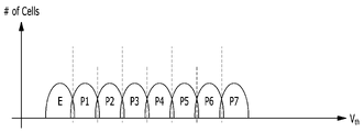
일 예로, 트리플 레벨 셀 메모리 블록들에서는, 프로그램 상태 및 이레이즈 상태를 지시하는 문턱 전압 분포가, 도 7에 도시한 바와 같이, 이상적으로 나타나며, 메모리 셀들에서 특성 열화가 발생할 경우에는, 도 8에 도시한 바와 같이, 프로그램 상태 및 이레이즈 상태를 지시하는 문턱 전압 분포가 변형되어 나타난다. 보다 구체적으로 설명하면, 트리플 레벨 셀 메모리 블록들에 포함된 싱글 메모리 셀에 3개의 데이터 비트(즉, k=3)를 프로그램할 경우, 23개(즉, 8개)의 문턱 전압 분포들 중 어느 하나의 문턱 전압 분포가 싱글 메모리 셀에 형성된다. 여기서, 복수의 메모리 셀들 간의 다수의 메모리 셀들 간의 미세한 전기적 특성의 차이로 인해, 동일한 데이터가 프로그램된 메모리 셀들 각각의 문턱 전압들은 일정한 범위의 문턱 전압 분포를 형성한다. 예컨대, 트리플 레벨 셀 메모리 블록들에서는, 7개의 프로그램 상태(state)의 문턱 전압 분포들(P1, P2, P3, P4, P5, P6, P7)과 하나의 이레이즈 상태(state)의 문턱 전압 분포(E)가 형성된다. 여기서, 트리플 레벨 셀 메모리 블록들에서의 문턱 전압 분포들은, 도 7에 도시한 바와 같이, 각각의 문턱 전압 분포들 간이 하나도 겹치지 않은 이상적인 문턱 전압 분포를 가지거나, 도 8에 도시한 바와 같이, 메모리 셀들의 특성 열화로 인해 문턱 전압 분포들이 이동 또는 변형되어, 각각의 문턱 전압 분포들 간이 중첩된 문턱 전압 분포를 가진다.For example, in triple-level cell memory blocks, the threshold voltage distribution indicating the program state and erase state appears ideal as shown in FIG. As shown, the threshold voltage distribution indicating the program state and the erase state is modified. More specifically, when three data bits (ie, k=3) are programmed in a single memory cell included in triple-level cell memory blocks, among 2 3 (ie, 8) threshold voltage distributions Any one threshold voltage distribution is formed in a single memory cell. Here, due to minute differences in electrical characteristics between the plurality of memory cells, threshold voltages of each of the memory cells programmed with the same data form a threshold voltage distribution within a certain range. For example, in triple level cell memory blocks, threshold voltage distributions of seven program states (P1, P2, P3, P4, P5, P6, P7) and one erase state (threshold voltage distribution) (E) is formed. Here, the threshold voltage distributions in the triple-level cell memory blocks have an ideal threshold voltage distribution in which each threshold voltage distribution does not overlap at all, as shown in FIG. 7, or as shown in FIG. The threshold voltage distributions are shifted or deformed due to the deterioration of characteristics of the cells, so that each threshold voltage distribution has an overlapping threshold voltage distribution.
여기서, 메모리 장치(150)의 메모리 블록들에서의 문턱 전압 분포가, 도 8에 도시한 바와 같이, 중첩된 문턱 전압 분포를 가질 경우에는 많은 에러 비트들이 포함될 수 있으며, 메모리 블록들에서 프로그램 상태들을 각각 지시하는 프로그램 전압 분포가 도 8에 도시한 바와 같이 중첩된 문턱 전압 분포를 가질 경우에는, 많은 에러 비트들로 인해 메모리 블록들에서 프로그램 동작들을 실패로 확인한 후, 메모리 블록들에서 실패된 프로그램 동작들에 대해서는 추가적인 프로그램 동작들을 수행한다. 이때, 본 발명의 실시 예에 따른 메모리 시스템에서는, 호스트(102)로부터 수신된 복수의 라이트 커맨드들에 해당하는 프로그램 동작들을, 메모리 장치(150)의 메모리 블록들에서 수행할 경우, 메모리 장치(150)의 메모리 블록들에서 프로그램 동작들의 수행에 상응한 프로그램 전압 분포를, 전류 감지 회로를 통해 확인한다. 특히, 본 발명의 실시 예에서는, 프로그램 동작들의 수행에 상응한 프로그램 전압 분포들이, 도 7 또는 도 8에 도시한 문턱 전압 분포들을 가질 경우, 전류 감지 회로를 통해 각각의 프로그램 전압 분포들의 패스/페일을 확인하며, 메모리 장치(150)의 메모리 블록들에서 수행된 프로그램 동작들의 성공/실패 여부를 확인한다. 그러면 여기서, 도 9를 참조하여, 본 발명의 실시 예에 따른 메모리 시스템에서 프로그램 동작들의 성공/실패 확인 동작에 대해, 보다 구체적으로 설명하기로 한다.Here, when the threshold voltage distribution in the memory blocks of the
도 9를 참조하면, 컨트롤러(130)는, 호스트(102)로부터 수신된 복수의 라이트 커맨드들에 해당하는 데이터를, 컨트롤러(130)의 메모리(144)에 저장한 후, 메모리(144)에 저장된 데이터를, 메모리 장치(150)의 메모리 다이들에 포함된 메모리 블록들에 프로그램하여 저장한다. 여기서, 컨트롤러(130)는, 메모리(144)에 저장된 제1데이터(910)를, 버퍼0을 통해 메모리 장치(150)의 메모리 다이0에 포함된 메모리 블록들에 프로그램하고, 메모리(144)에 저장된 제2데이터(920)를, 버퍼1을 통해 메모리 장치(150)의 메모리 다이1에 포함된 메모리 블록들에 프로그램한다. 또한, 컨트롤러(130)는, 호스트(102)로부터 수신된 복수의 리드 커맨드들에 해당하는 데이터를, 메모리 장치(150)의 메모리 다이들에 포함된 메모리 블록들에서 리드하고, 리드된 데이터를 컨트롤러(130)의 메모리(144)에 저장한 후 호스트(102)로 제공한다. 여기서, 컨트롤러(130)는, 버퍼0을 통해 메모리 장치(150)의 메모리 다이0에 포함된 메모리 블록들에서 데이터를 리드한 후, 리드된 데이터를 메모리(144)에 저장하며, 또한 버퍼1을 통해 메모리 장치(150)의 메모리 다이1에 포함된 메모리 블록들에서 데이터를 리드한 후, 리드된 데이터를 메모리(144)에 저장한다. 그리고, 컨트롤러(130)는, ECC 유닛(138)을 통해 메모리(144)에 저장된 제1데이터(910) 및 제2데이터(920)의 에러 비트를 정정한 후 호스트(102)로 제공한다.Referring to FIG. 9 , the
특히, 컨트롤러(130)는, 메모리(144)에 저장된 제1데이터(910) 및 제2데이터(920)를 메모리 장치(150)의 메모리 다이0 및 메모리 다이1에 포함된 메모리 블록들에 프로그램하여 저장한 후, 메모리 블록들에서 수행된 프로그램 동작들에 대한 성공/실패 여부를 확인한다. 일 예로, 컨트롤러(130)는, 메모리(144)에 저장된 제1데이터(910)를 메모리 다이0의 메모리 블록들에 프로그램하여 저장한 후, 메모리 다이0의 메모리 블록들에서 수행된 프로그램 동작들에 대한 성공/실패 여부의 결과를 메모리 장치(150)로부터 수신한다. 여기서, 메모리 장치(150)는, 제1데이터(910)에 대해 프로그램 동작이 수행된 메모리 다이0의 메모리 블록들에서의 문턱 전압 분포들을, 체크 유닛0을 통해 확인하며, 문턱 전압 분포들에 상응하여 프로그램 전압 분포들의 패스/페일을 확인함으로써, 프로그램 동작들의 성공/실패 여부를 확인한 후, 성공/실패 여부의 결과를 컨트롤러(130)로 전송한다. 또한, 컨트롤러(130)는, 메모리(144)에 저장된 제2데이터(920)를 메모리 다이1의 메모리 블록들에 프로그램하여 저장한 후, 메모리 다이1의 메모리 블록들에서 수행된 프로그램 동작들에 대한 성공/실패 여부의 결과를 메모리 장치(150)로부터 수신한다. 여기서, 메모리 장치(150)는, 제2데이터(920)에 대해 프로그램 동작이 수행된 메모리 다이1의 메모리 블록들에서의 문턱 전압 분포들을, 체크 유닛1을 통해 확인하며, 문턱 전압 분포들에 상응하여 프로그램 전압 분포들의 패스/페일을 확인함으로써, 프로그램 동작들의 성공/실패 여부를 확인한 후, 성공/실패 여부의 결과를 컨트롤러(130)로 전송한다.In particular, the
여기서, 본 발명의 실시 예에서는, 설명의 편의를 위해, 체크 유닛들이 메모리 장치(150)에 포함된 각각의 메모리 다이들에 대응되도록 존재하는 것을 일 예로 하여 설명하지만, 메모리 장치(150)를 구현하는 메모리 셀 어레이 전체에 대응되도록 존재하거나, 또는 각각의 메모리 다이들에 포함된 플래인들 또는 각각의 플래인들에 포함된 메모리 블록들에 각각 대응되도록 존재할 수도 있다. 또한, 본 발명의 실시 예에서는, 설명의 편의를 위해, 체크 유닛들이, 메모리 장치(150)의 내부 및 메모리 다이들 외부에 존재하는 것을 일 예로 하여 설명하지만, 메모리 장치(150)의 외부 또는 메모리 다이들 내부 등에 존재할 수도 있으며, 아울러 컨트롤러(130)의 내부에 존재할 수도 있다.Here, in the embodiment of the present invention, for convenience of explanation, it is described as an example that the check units exist to correspond to each of the memory dies included in the
또한, 체크 유닛들은, 메모리 장치(150) 또는 각각의 메모리 다이들 내에 구현된 메모리 셀 어레이에서의 동작 상태를 확인하는 동작 체크 유닛, 동작 체크 유닛을 통해 확인한 페일 비트(fail bit)들을 카운팅하는 카운팅 유닛, 카운팅 유닛을 통해 카운팅된 페일 비트 수를 합산하는 합산 유닛, 합산 페일 비트 수와 임계값 간을 비교하는 비교 유닛, 및 페일 비트 수와 합산 페일 비트 수 및 임계값 등을 저장하는 저장 유닛을, 포함한다. 여기서, 동작 체크 유닛은, 전류 감지 회로를 포함하며, 전류 감지 회로를 통해 메모리 셀 어레이에서의 문턱 전압 분포들을 확인함으로써, 프로그램 동작들이 수행된 메모리 블록들에서의 프로그램 전압 분포들을 확인하며, 또한 프로그램 동작들이 수행된 메모리 블록들에서 프로그램 전압 분포들의 패스/페일을 지시하는 신호를 생성한다. 또한, 카운팅 유닛은, 동작 체크 유닛을 통해 확인한 프로그램 전압 분포들의 패스/페일에서, 프로그램 전압 분포들이 페일인 메모리 셀들을 카운팅하며, 그에 따라 동작 체크 유닛을 통해 확인한 프로그램 전압 분포들에서 페일 비트들을 카운팅한다. 그리고, 합산 유닛은, 카운팅 유닛을 통해 카운팅된 페일 비트 수를 합산하며, 특히 임의의 페이지 그룹들 별로 페일 비트 수를 각각 합산한다. 아울러, 비교 유닛은, 페일 비트 수와 임계값 간을 비교하며, 특히 합산 페일 비트 수와 임계값 간을 비교한 후, 비교 결과에 따라 프로그램 동작들의 성공/실패를 지시하는 신호를 컨트롤러(130)로 전송한다. 그리고, 저장 유닛은, 페일 비트 수와 합산 페일 비트 수 및 임계값 뿐만 아니라, 동작 체크 유닛에서 확인된 프로그램 전압 분포들의 패스/페일에 대한 신호값과, 비교 유닛에서 확인된 프로그램 동작들의 성공/실패에 대한 신호값을 저장하며, 또한 메모리 장치(150)의 버퍼들에 포함될 수 있으며, 특히 메모리 장치(150)에서 레지스터들로 구현된 버퍼들에 포함될 수 있다. 여기서, 본 발명의 실시 예에서는, 설명의 편의를 위해, 메모리 장치(150)에 포함된 트리플 레벨 셀 메모리 블록들에서 프로그램 동작들이 수행될 경우, 도 7 및 도 8의 문턱 전압 분포들을 갖는 프로그램 전압 분포들의 패스/페일을 확인한 후, 프로그램 동작들의 성공/실패를 확인함을 일 예로 하여, 보다 구체적으로 설명하기로 한다.In addition, the check units include an operation check unit for checking an operating state of the memory cell array implemented in the
예컨대, 체크 유닛들은, 메모리 장치(150)의 메모리 블록들에서 프로그램 동작들을 수행한 후, 프로그램 동작들이 수행된 메모리 블록들에서의 문턱 전압 분포들을, 프로그램 전압 분포들로 확인한다. 여기서, 체크 유닛들은, 프로그램 전압 분포들에서 최상위 레벨의 프로그램 전압 분포(P7) 또는 최하위 레벨의 프로그램 전압 분포(P1)에 대한 패스/페일을 확인하며, 특히 최상위 레벨의 프로그램 전압 분포(P7)에 대한 패스/페일을 확인한 후, 최상위 레벨의 프로그램 전압 분포(P7)가 패스일 경우, 나머지 다른 프로그램 전압 분포들(P1, P2, P3, P4, P5, P6)에 대한 패스/페일을 확인한다. 여기서, 체크 유닛들은, 최상위 레벨의 프로그램 전압 분포(P7)가 페일일 경우, 메모리 장치(150)의 메모리 블록들에서 수행된 프로그램 동작들이 모두 실패임을 지시하는 신호, 예컨대 프로그램 실패 상태(program fail status) 신호를 컨트롤러(130)로 전송한다.For example, after performing program operations on memory blocks of the
또한, 체크 유닛들은, 최상위 레벨의 프로그램 전압 분포(P7)뿐만 아니라, 나머지 다른 프로그램 전압 분포들(P1, P2, P3, P4, P5, P6), 즉 모든 프로그램 전압 분포들(P1, P2, P3, P4, P5, P6, P7)이 패스일 경우, 메모리 장치(150)의 메모리 블록들에서 수행한 프로그램 동작들의 성공을 지시하는 신호를 컨트롤러(130)로 전송한다. 여기서, 체크 유닛들은, 모든 프로그램 전압 분포들(P1, P2, P3, P4, P5, P6, P7)이 패스일 경우, 메모리 장치(150)의 메모리 블록들에서 수행된 프로그램 동작들이 모두 정상(normal) 성공임을 지시하는 신호, 예컨대 프로그램 성공 상태1(program success status1) 신호를 컨트롤러(130)로 전송한다.In addition, the check units are not only the top level program voltage distribution (P7), but also the other program voltage distributions (P1, P2, P3, P4, P5, P6), that is, all program voltage distributions (P1, P2, P3). , P4, P5, P6, and P7) are pass, signals indicating success of program operations performed in the memory blocks of the
그리고, 체크 유닛들은, 최상위 레벨의 프로그램 전압 분포(P7)가 패스이고, 나머지 다른 프로그램 전압 분포들(P1, P2, P3, P4, P5, P6) 중 적어도 하나의 프로그램 전압 분포가 페일일 경우, 프로그램 전압 분포의 페일이 발생한 프로그램 전압 분포들에 대한 페일 비트들을 각각 확인한 후, 프로그램 전압 분포들(P1, P2, P3, P4, P5, P6, P7)에서의 페일 비트들을 카운팅한다. 여기서, 본 발명의 실시 예에 따른 메모리 시스템에서는, 모든 프로그램 전압 분포들(P1, P2, P3, P4, P5, P6, P7)에서, 적어도 하나의 페일이 발생한 프로그램 전압 분포가 존재할 경우, 모든 프로그램 전압 분포들(P1, P2, P3, P4, P5, P6, P7)에서 패스가 될 때까지, 기 설정된 최대 루프(max loop)만큼 추가적인 프로그램 동작들을 수행하지 않고, 모든 프로그램 전압 분포들(P1, P2, P3, P4, P5, P6, P7)에서의 페일 비트들을 각각 확인하며, 추가적인 프로그램 동작들의 수행을 최소화함으로써, 메모리 셀들의 특성 열화 및 동작 속도 증가를 감소시키며, 아울러 메모리 장치(150)의 워드라인들에서 스트링 스트레스(string stress)를 최소화하여 메모리 장치(150)의 신뢰도를 향상시킨다.Further, in the check units, when the highest level program voltage distribution P7 is a pass and at least one of the other program voltage distributions P1, P2, P3, P4, P5, and P6 is a fail, After checking each of the fail bits of the program voltage distributions in which the failure of the program voltage distribution occurred, the fail bits in the program voltage distributions P1 , P2 , P3 , P4 , P5 , P6 , and P7 are counted. Here, in the memory system according to an exemplary embodiment of the present invention, when at least one program voltage distribution in which a failure occurs is present among all program voltage distributions P1, P2, P3, P4, P5, P6, and P7, all program voltage distributions exist. All program voltage distributions (P1, P2, P3, P4, P5, P6, and P7) respectively check the fail bits, and by minimizing the execution of additional program operations, the deterioration of the characteristics of the memory cells and the increase in the operating speed are reduced, and in addition, the performance of the
다시 말해, 체크 유닛들은, 모든 프로그램 전압 분포들(P1, P2, P3, P4, P5, P6, P7)에서, 적어도 하나의 페일이 발생한 프로그램 전압 분포가 존재할 경우, 제1프로그램 전압 분포(P1)에서의 제1페일 비트들을 확인한 후 카운팅하고, 제2프로그램 전압 분포(P2)에서의 제2페일 비트들을 확인한 후 카운팅하며, 제3프로그램 전압 분포(P3)에서의 제3페일 비트들을 확인한 후 카운팅하고, 제4프로그램 전압 분포(P4)에서의 제4페일 비트들을 확인한 후 카운팅하며, 제5프로그램 전압 분포(P5)에서의 제5페일 비트들을 확인한 후 카운팅하고, 제6프로그램 전압 분포(P6)에서의 제6페일 비트들을 확인한 후 카운팅하며, 제7프로그램 전압 분포(P7)에서의 제7페일 비트들을 확인한 후 카운팅한다.In other words, the check units determine the first program voltage distribution P1 when at least one program voltage distribution in which a failure occurs exists among all program voltage distributions P1 , P2 , P3 , P4 , P5 , P6 , and P7 . Counting after checking the first fail bits in P2, counting after checking the second fail bits in the second program voltage distribution P2, counting after checking the third fail bits in the third program voltage distribution P3 counting after checking the 4th fail bits in the 4th program voltage distribution P4, counting after checking the 5th fail bits in the 5th program voltage distribution P5, and counting after checking the 6th program voltage distribution P6 Counting is performed after checking the 6th fail bits in , and counting is performed after checking the 7th fail bits in the 7th program voltage distribution P7 .
그리고, 체크 유닛들은, 모든 프로그램 전압 분포들(P1, P2, P3, P4, P5, P6, P7)에서 카운팅된 페일 비트 수들을 합산한다. 여기서, 체크 유닛들은, 모든 프로그램 전압 분포들(P1, P2, P3, P4, P5, P6, P7)에서의 페일 비트 수들을, 프로그램 전압 분포 그룹들 별로 합산한다. 여기서, 체크유닛들은, 메모리 장치(150)에 포함된 메모리 블록들에 상응하여 프로그램 전압 분포 그룹들 별로 합산하며, 특히 1비트 또는 2비트 이상의 멀티 비트를 저장하는 메모리 블록들에 상응하여, 단일 프로그램 전압 분포 그룹 또는 멀티 프로그램 전압 분포 그룹들(일 예로, 단일 레벨 셀 메모리 블록에서는 단일 프로그램 전압 분포 그룹, 멀티 레벨 셀 메모리 블록에서는 2개의 프로그램 전압 분포 그룹, 트리플 레벨 셀 메모리 블록에서는 3개의 프로그램 전압 분포 그룹, 및 쿼드러플 레벨 셀 메모리 블록에서는 4개의 프로그램 전압 분포 그룹) 별로, 합산한다.And, the check units sum up the counted number of fail bits in all program voltage distributions P1, P2, P3, P4, P5, P6, and P7. Here, the check units sum up the number of fail bits in all program voltage distributions P1 , P2 , P3 , P4 , P5 , P6 , and P7 for each program voltage distribution group. Here, the check units are summed for each program voltage distribution group corresponding to the memory blocks included in the
예컨대, 체크 유닛들은, 제1프로그램 전압 분포 그룹에 포함되는 프로그램 전압 분포들(P3, P7)의 페일 비트 수들을 합산하고, 제2프로그램 전압 분포 그룹에 포함되는 프로그램 전압 분포들(P2, P4, P6)의 페일 비트 수들을 합산하며, 제3프로그램 전압 분포 그룹에 포함되는 프로그램 전압 분포들(P1, P5)의 페일 비트 수들을 합산한다. 여기서, 제1프로그램 전압 분포 그룹은, 프로그램 동작들이 수행된 메모리 장치(150)의 메모리 블록들에서 LSB(Least Significant Bit) 페이지들에 해당하는 프로그램 전압 분포들(P3, P7)을 포함하고, 제2프로그램 전압 분포 그룹은, 프로그램 동작들이 수행된 메모리 장치(150)의 메모리 블록들에서 CSB(Central Significant Bit) 페이지들에 해당하는 프로그램 전압 분포들(P2, P4, P6)을 포함하며, 제3프로그램 전압 분포 그룹은, 프로그램 동작들이 수행된 메모리 장치(150)의 메모리 블록들에서 MSB(Most Significant Bit) 페이지들에 해당하는 프로그램 전압 분포들을 포함한다. 즉, 체크 유닛들은, 메모리 블록들에서 LSB 페이지들에 해당하는, 제3프로그램 전압 분포(P3)에서의 제3페일 비트들을 카운팅한 제3페일 비트 수와, 제7프로그램 전압 분포(P7)에서의 제7페일 비트들을 카운팅한 제7페일 비트 수를, 합산한다. 그리고, 체크 유닛들은, 메모리 블록들에서 CSB 페이지들에 해당하는, 제2프로그램 전압 분포(P2)에서의 제2페일 비트들을 카운팅한 제2페일 비트 수와, 제4프로그램 전압 분포(P4)에서의 제4페일 비트들을 카운팅한 제4페일 비트 수, 및 제6프로그램 전압 분포(P6)에서의 제6페일 비트들을 카운팅한 제6페일 비트 수를, 합산한다. 아울러, 체크 유닛들은, 메모리 블록들에서 MSB 페이지들에 해당하는, 제1프로그램 전압 분포(P1)에서의 제1페일 비트들을 카운팅한 제1페일 비트 수와, 제5프로그램 전압 분포(P5)에서의 제5페일 비트들을 카운팅한 제5페일 비트 수를, 합산한다.For example, the check units sum the number of fail bits of the program voltage distributions P3 and P7 included in the first program voltage distribution group, and the program voltage distributions P2, P4, and P4 included in the second program voltage distribution group. The number of fail bits of P6) is summed, and the numbers of fail bits of program voltage distributions P1 and P5 included in the third program voltage distribution group are summed. Here, the first program voltage distribution group includes program voltage distributions P3 and P7 corresponding to Least Significant Bit (LSB) pages in memory blocks of the
또한, 체크 유닛들은, 모든 프로그램 전압 분포들(P1, P2, P3, P4, P5, P6, P7)에서 카운팅된 페일 비트 수들과 임계값을 비교한다. 특히, 체크 유닛들은, 모든 프로그램 전압 분포들(P1, P2, P3, P4, P5, P6, P7)에서 프로그램 전압 분포 그룹들 별로 각각 합산된 합산 비트 수와, 임계값을 비교한 후, 비교 결과에 상응하여 메모리 장치(150)의 메모리 블록들에서 수행된 프로그램 동작들에 대한 성공/실패를 지시하는 신호를 컨트롤러(130)로 전송한다. 여기서, 체크 유닛들은, 제1프로그램 전압 분포 그룹의 제3페일비트 수와 제7페일 비트 수를 합산된 제1합산 비트 수와, 임계값을 비교하고, 제2프로그램 전압 분포 그룹의 제2페일 비트 수와 제4페일 비트 수 및 제6페일 비트 수가 합산된 제2합산 비트 수와, 임계값을 비교하며, 제3프로그램 전압 분포 그룹의 제1페일 비트 수와 제5페일 비트 수가 합산된 제3합산 비트 수와, 임계값을 비교한다. 여기서, 임계값은, ECC 유닛(138)을 통해 정정 가능한 에러 비트 한계치에 상응하여 결정되며, 또한 컨트롤러(130)에서 결정되거나 또는 체크 유닛들에서 결정된 후 저장 유닛에 저장되며, 컨트롤러(130)에서 결정될 경우 프로세서(134) 또는 ECC 유닛(138)에서 결정될 수 있다.Also, the check units compare the number of fail bits counted in all program voltage distributions P1, P2, P3, P4, P5, P6, and P7 with the threshold value. In particular, the check units compare the total number of bits added for each program voltage distribution group in all program voltage distributions (P1, P2, P3, P4, P5, P6, P7) with a threshold value, and then compare the comparison result. Correspondingly, signals indicating success/failure of program operations performed in the memory blocks of the
그리고, 체크 유닛들은, 제1합산 비트 수와 임계값, 제2합산 비트 수와 입계값, 및 제3합산 비트 수와 임계값 간, 각각의 비교 결과, 적어도 하나의 합산 비트 수가 임계값을 초과할 경우, 메모리 장치(150)의 메모리 블록들에서 수행된 프로그램 동작들이 모두 실패임을 지시하는 신호, 예컨대 프로그램 실패 상태 신호를 컨트롤러(130)로 전송한다. 여기서, 합산 비트 수가 임계값을 초과하는 프로그램 전압 분포 그룹(이하, '페일 프로그램 전압 분포 그룹'이라 칭하기로 함)에는, 많은 에러 비트들, 특히 임계값 이상의 에러 비트들을 갖는 프로그램 전압 분포들이 포함되며, 페일 프로그램 전압 분포 그룹에 포함된 에러 비트들은, ECC 유닛(138)을 통해 정정 가능한 에러 비트 한계치를 초과한다. 즉, 메모리 블록들에서 페일 프로그램 전압 분포 그룹에 해당하는 페이지들에는, ECC 유닛(138)을 통해 정정 가능한 에러 비트 한계치를 초과한 에러 비트들이 프로그램된 상태이므로, 체크 유닛들은 프로그램 실패 상태 신호를 컨트롤러(130)로 전송한다.In addition, the check units may perform a comparison between the first sum bit number and the threshold value, the second sum bit number and the threshold value, and the third sum bit number and the threshold value, and as a result of each comparison, at least one sum bit number exceeds the threshold value. In this case, a signal indicating that all program operations performed in the memory blocks of the
또한, 체크 유닛들은, 제1합산 비트 수와 임계값, 제2합산 비트 수와 입계값, 및 제3합산 비트 수와 임계값 간, 각각의 비교 결과, 각각의 합산 비트 수가 임계값보다 모두 작을 경우, 메모리 장치(150)의 메모리 블록들에서 수행된 프로그램 동작들이 부분(partial) 성공임을 지시하는 신호, 예컨대 프로그램 성공 상태2(program success status2) 신호를 컨트롤러(130)로 전송한다. 여기서, 각각의 합산 비트 수가 임계값보다 모두 작은 프로그램 전압 분포 그룹들(이하, '부분 프로그램 전압 분포 그룹'이라 칭하기로 함)에는, 적은 에러 비트들, 특히 임계값 이하의 에러 비트들을 갖는 프로그램 전압 분포들이 포함되며, 부분 프로그램 전압 분포 그룹에 포함된 에러 비트들은, ECC 유닛(138)을 통해 정정 가능한 에러 비트 한계치 이내가 된다. 즉, 메모리 블록들에서 부분 프로그램 전압 분포 그룹에 해당하는 페이지들에는, ECC 유닛(138)을 통해 정정 가능한 에러 비트 한계치 이내의 에러 비트들이 프로그램된 상태이므로, 체크 유닛들은 프로그램 성공 상태2 신호를 컨트롤러(130)로 전송한다.In addition, the check units determine whether, as a result of comparison between the first summed number of bits and the threshold value, the second summed number of bits and the threshold value, and the third summed number of bits and the threshold value, each summed number of bits is smaller than the threshold value. In this case, a signal indicating that the program operations performed in the memory blocks of the
아울러, 컨트롤러(130)는, 메모리 장치(150)의 체크 유닛들로부터 프로그램 실패 상태 신호를 수신할 경우, 메모리 장치(150)의 메모리 블록들에서 수행된 프로그램 동작들이 모두 실패임을 확인하며, 실패된 프로그램 동작들에 대한 프로그램 동작들을 다시 수행하거나, 또는 호스트(102)로부터 수신된 라이트 커맨드들의 응답으로 실패를 지시하는 신호를 호스트(102)로 전송한다. 또한, 컨트롤러(130)는, 메모리 장치(150)의 체크 유닛들로부터 프로그램 성공 상태1 신호를 수신할 경우, 메모리 장치(150)의 메모리 블록들에서 수행된 프로그램 동작들이 모두 정상 성공임을 확인하며, 호스트(102)로부터 수신된 라이트 커맨드들의 응답으로 성공을 지시하는 신호를 호스트(102)로 전송하고, 또한 호스트(102)로부터 수신된 다른 커맨드들에 해당하는 커맨드 동작들을 수행한다.In addition, when receiving a program failure status signal from the check units of the
그리고, 컨트롤러(130)는, 메모리 장치(150)의 체크 유닛들로부터 프로그램 성공 상태2 신호를 수신할 경우, 메모리 장치(150)의 메모리 블록들에서 수행된 프로그램 동작들이 부분 성공임을 확인하며, 호스트(102)로부터 수신된 라이트 커맨드들의 응답으로 성공을 지시하는 신호를 호스트(102)로 전송한다. 아울러, 컨트롤러(130)는, 메모리 장치(150)의 체크 유닛들로부터 수신된 프로그램 성공 상태2 신호에 상응하여, 메모리 장치(150)의 메모리 블록들에서 부분 성공 프로그램 동작들에 해당하는 데이터(이하, '부분 성공 프로그램 데이터'라 칭하기로 함)에 대한, 카피 동작을 수행한다. 여기서, 컨트롤러(130)는, 메모리 장치(150)의 메모리 블록들에서 부분 프로그램 전압 분포 그룹에 해당하는 페이지들을 확인하고, 부분 프로그램 전압 분포 그룹의 페이지들에 저장된 부분 성공 프로그램 데이터를 리드한 후, 리드된 부분 성공 프로그램 데이터를 메모리 장치(150)의 메모리 블록들에 저장한다. 이때, 컨트롤러(130)는, 리드된 부분 성공 프로그램 데이터를 컨트롤러(130)의 메모리(144)에 저장한 후, ECC 유닛(138)을 통해 에러 정정 동작을 수행하며, 에러 정정된 부분 성공 프로그램 데이터를 메모리 장치(150)의 메모리 블록들에 저장한다.Further, when receiving the
여기서, 부분 프로그램 전압 분포 그룹의 페이지들이, 제1메모리 블록의 제1LSB 페이지들과 제1CSB 페이지들 및 제1MSB 페이지들일 경우, 컨트롤러(130)는, 제1LSB 페이지들과 제1CSB 페이지들 및 제1MSB 페이지들에 저장된 부분 성공 프로그램 데이터를, 제1메모리 블록의 제2LSB 페이지들과 제2CSB 페이지들 및 제2MSB 페이지들에 저장하거나, 제2메모리 블록의 제1LSB 페이지들과 제1CSB 페이지들 및 제1MSB 페이지들에 저장한다. 또한, 부분 프로그램 전압 분포 그룹의 페이지들이, 제1메모리 블록의 제1LSB 페이지들과 제1CSB 페이지들 및 제1MSB 페이지들일 경우, 컨트롤러(130)는, 제1LSB 페이지들과 제1CSB 페이지들 및 제1MSB 페이지들 중에서 임의의 페이지들에 저장된 부분 성공 프로그램 데이터, 예컨대 제1MSB 페이지들에 저장된 부분 성공 프로그램 데이터를, 제1메모리 블록의 제2MSB 페이지들에 저장하거나, 제2메모리 블록의 제1MSB 페이지들에 저장한다. 여기서, 제1메모리 블록의 제1LSB 페이지들과 제1CSB 페이지들 및 제1MSB 페이지들 중에서 임의의 페이지들은, 페일 비트들이 포함된 페이지들이고, 나머지 페이지들은 페일 비트들이 포함되지 않은 페이지들이 된다. 즉, 컨트롤러(130)는, 부분 성공 프로그램 데이터의 전체 데이터에 대한 카피 동작을 수행하거나, 부분 성공 프로그램 데이터에서 페일 비트들이 포함된 부분 데이터에 대한 카피 동작을 수행한다. 그러면 여기서, 도 10을 참조하여 본 발명의 실시 예에 따른 메모리 시스템에서의 데이터를 처리하는 동작에 대해서 보다 구체적으로 설명하기로 한다.Here, when the pages of the partial program voltage distribution group are the 1st LSB pages, the 1st CSB pages, and the 1st MSB pages of the first memory block, the
도 10은 본 발명의 실시 예에 따른 메모리 시스템에서의 데이터를 처리하는 동작 과정을 개략적으로 도시한 도면이다.10 is a diagram schematically illustrating an operation process of processing data in a memory system according to an embodiment of the present invention.
도 10을 참조하면, 메모리 시스템(110)은, 1005단계에서, 호스트(102)로부터 수신된 복수의 라이트 커맨드들에 해당하는 프로그램 동작들을, 메모리 장치(150)의 메모리 블록들에서 수행한다.Referring to FIG. 10 , in
그리고, 메모리 시스템(110)은, 1010단계에서, 메모리 장치(150)의 메모리 블록들에서 수행된 프로그램 동작들에 대한 프로그램 전압 분포들을 확인하며, 1015단계에서, 프로그램 전압 분포들에 대한 패스/페일을 확인한다.In
또한, 메모리 시스템(110)은, 프로그램 전압 분포들에 대한 패스/페일을 확인한 결과, 모든 프로그램 전압 분포들이 패스일 경우, 1020단계에서, 메모리 장치(150)의 메모리 블록들에서 수행된 프로그램 동작들이 모두 성공임을 확인한다.In addition, as a result of checking pass/fail for the program voltage distributions, the
아울러, 메모리 시스템(110)은, 프로그램 전압 분포들에 대한 패스/페일을 확인한 결과, 프로그램 전압 분포들에서 페일이 발생할 경우, 1025단계에서, 프로그램 전압 분포들에서의 페일 비트들을 각각 확인한 후 페일 비트들을 카운팅한다.In addition, as a result of checking the pass/fail of the program voltage distributions, the
그런 다음, 메모리 시스템(110)은, 1030단계에서, 카운팅된 페일 비트 수와 임계값을 비교하며, 특히 프로그램 전압 분포들에서의 페일 비트 수를, 프로그램 전압 분포 그룹들 별로 각각 합산한 후, 합산 페일 비트 수와 임계값을 비교한다.Then, in
그리고, 메모리 시스템은, 프로그램 전압 분포들에서의 페일 비트 수, 특히 합산 페일 비트 수가 임계값을 초과할 경우, 1035단계에서, 메모리 장치(150)의 메모리 블록들에서 수행된 프로그램 동작들이 모두 실패임을 확인한다.The memory system determines that all program operations performed in the memory blocks of the
또한, 메모리 시스템은, 프로그램 전압 분포들에서의 페일 비트 수, 특히 합산 페일 비트 수가 임계값보다 작을 경우에는, 메모리 장치(150)의 메모리 블록들에서 수행된 프로그램 동작들이 부분 성공임을 확인하며, 부분 성공 프로그램 데이터에 대한 카피 동작을 수행한다.In addition, when the number of fail bits in the program voltage distributions, in particular, the sum of the number of fail bits is smaller than the threshold value, the memory system confirms that the program operations performed in the memory blocks of the
여기서, 메모리 장치(150)의 메모리 블록들에서 호스트(102)로부터 수신된 복수의 라이트 커맨드들에 해당하는 프로그램 동작들을 수행할 경우, 프로그램 동작들의 수행에 따른 프로그램 전압 분포들 별로 패스/페일을 확인하고, 프로그램 전압 분포들 별 패스/페일을 통해 메모리 장치(150)의 메모리 블록들에서 수행된 프로그램 동작들의 성공/실패 여부를 확인하며, 프로그램 동작들의 성공/실패에 따른 추가적인 프로그램 동작들의 수행에 대해서는, 앞서 도 5 내지 도 9를 참조하여 구체적으로 설명하였으므로, 여기서는 그에 관한 구체적인 설명을 생략하기로 한다. 그러면 이하에서는, 도 11 내지 도 19를 참조하여, 본 발명의 실시 예에 따라 도 1 내지 도 10에서 설명한 메모리 장치(150) 및 컨트롤러(130)를 포함하는 메모리 시스템(110)이 적용된 데이터 처리 시스템 및 전자 기기들에 대해서 보다 구체적으로 설명하기로 한다.Here, when program operations corresponding to the plurality of write commands received from the
도 11은 본 발명의 실시 예에 따른 메모리 시스템을 포함하는 데이터 처리 시스템의 다른 일 예를 개략적으로 도시한 도면이다. 여기서, 도 11은 본 발명의 실시 예에 따른 메모리 시스템이 적용된 메모리 카드 시스템을 개략적으로 도시한 도면이다.11 is a diagram schematically illustrating another example of a data processing system including a memory system according to an embodiment of the present invention. Here, FIG. 11 is a diagram schematically illustrating a memory card system to which a memory system according to an embodiment of the present invention is applied.
도 11을 참조하면, 메모리 카드 시스템(6100)은, 메모리 컨트롤러(6120), 메모리 장치(6130), 및 커넥터(6110)를 포함한다.Referring to FIG. 11 , a
보다 구체적으로 설명하면, 메모리 컨트롤러(6120)는, 비휘발성 메모리로 구현된 메모리 장치(6130)와 연결되며, 메모리 장치(6130)를 액세스하도록 구현된다. 예컨대, 메모리 컨트롤러(6120)는, 메모리 장치(6130)의 리드, 라이트, 이레이즈, 및 백그라운드(background) 동작 등을 제어하도록 구현된다. 그리고, 메모리 컨트롤러(6120)는, 메모리 장치(6130) 및 호스트(Host) 사이에 인터페이스를 제공하도록 구현되며, 메모리 장치(6130)를 제어하기 위한 펌웨어(firmware)를 구동하도록 구현된다. 즉, 메모리 컨트롤러(6120)는, 도 1에서 설명한 메모리 시스템(110)에서의 컨트롤러(130)에 대응되며, 메모리 장치(6130)는, 도 1에서 설명한 메모리 시스템(110)에서의 메모리 장치(150)에 대응될 수 있다.More specifically, the
그에 따라, 메모리 컨트롤러(6120)는, 램(RAM: Random Access Memory), 프로세싱 유닛(processing unit), 호스트 인터페이스(host interface), 메모리 인터페이스(memory interface), 에러 정정부와 같은 구성 요소들을 포함할 수 있다.Accordingly, the
아울러, 메모리 컨트롤러(6120)는, 커넥터(6110)를 통해 외부 장치, 예컨대 도 1에서 설명한 호스트(102)와 통신할 수 있다. 예컨대, 메모리 컨트롤러(6120)는, 도 1에서 설명한 바와 같이, USB(Universal Serial Bus), MMC(multimedia card), eMMC(embeded MMC), PCI(peripheral component interconnection), PCIe(PCI express), ATA(Advanced Technology Attachment), Serial-ATA, Parallel-ATA, SCSI(small computer small interface), ESDI(enhanced small disk interface), IDE(Integrated Drive Electronics), 파이어와이어(Firewire), UFS(Universal Flash Storage), WIFI, Bluetooth 등과 같은 다양한 통신 규격들 중 적어도 하나를 통해 외부 장치와 통신하도록 구성될 수 있으며, 그에 따라 유선/무선 전자 기기들, 특히 모바일 전자 기기 등에 본 발명의 실시 예에 따른 메모리 시스템 및 데이터 처리 시스템이 적용될 수 있다.In addition, the
그리고, 메모리 장치(6130)는, 비휘발성 메모리로 구현, 예컨대 EPROM(Electrically Erasable and Programmable ROM), 낸드 플래시 메모리, 노어 플래시 메모리, PRAM(Phase-change RAM), ReRAM(Resistive RAM), FRAM(Ferroelectric RAM), STT-MRAM(Spin-Torque Magnetic RAM) 등과 같은 다양한 비휘발성 메모리들로 구현될 수 있다.In addition, the
아울러, 메모리 컨트롤러(6120) 및 메모리 장치(6130)는, 하나의 반도체 장치로 집적될 수 있으며, 일 예로 하나의 반도체 장치로 집적되어 솔리드 스테이트 드라이브(SSD: Solid State Drive)를 구성할 수 있으며, PC 카드(PCMCIA), 컴팩트 플래시 카드(CF), 스마트 미디어 카드(SM, SMC), 메모리 스틱, 멀티미디어 카드(MMC, RS-MMC, MMCmicro, eMMC), SD 카드(SD, miniSD, microSD, SDHC), 유니버설 플래시 기억장치(UFS) 등과 같은 메모리 카드를 구성할 수 있다.In addition, the
도 12는 본 발명의 실시 예에 따른 메모리 시스템을 포함하는 데이터 처리 시스템의 다른 일 예를 개략적으로 도시한 도면이다.12 is a diagram schematically illustrating another example of a data processing system including a memory system according to an embodiment of the present invention.
도 12를 참조하면, 데이터 처리 시스템(6200)은, 적어도 하나의 비휘발성 메모리로 구현된 메모리 장치(6230), 및 메모리 장치(6230)를 제어하는 메모리 컨트롤러(6220)를 포함한다. 여기서, 도 10에 도시한 데이터 처리 시스템(6200)은, 도 1에서 설명한 바와 같이, 메모리 카드(CF, SD, microSD, 등), USB 저장 장치 등과 같은 저장 매체가 될 수 있으며, 메모리 장치(6230)는, 도 1에서 설명한 메모리 시스템(110)에서의 메모리 장치(150)에 대응되고, 메모리 컨트롤러(6220)는, 도 1에서 설명한 메모리 시스템(110)에서의 컨트롤러(130)에 대응될 수 있다.Referring to FIG. 12 , the
그리고, 메모리 컨트롤러(6220)는, 호스트(6210)의 요청에 응답하여 메모리 장치(6230)에 대한 리드, 라이트, 이레이즈 동작 등을 제어하며, 메모리 컨트롤러(6220)는 적어도 하나의 CPU(6221), 버퍼 메모리, 예컨대 RAM(6222), ECC 회로(6223), 호스트 인터페이스(6224), 및 메모리 인터페이스, 예컨대 NVM 인터페이스(6225)를 포함한다.The
여기서, CPU(6221)는, 메모리 장치(6230)에 대한 전반적인 동작, 예컨대 읽기, 쓰기, 파일 시스템 관리, 배드 페이지 관리 등)을 제어할 수 있다. 그리고, RAM(6222)는, CPU(6221)의 제어에 따라 동작하며, 워크 메모리(work memory), 버퍼 메모리(buffer memory), 캐시 메모리(cache memory) 등으로 사용될 수 있다. 여기서, RAM(6222)이 워크 메모리로 사용되는 경우에, CPU(6221)에서 처리된 데이터가 임시 저장되며, RAM(6222)이 버퍼 메모리로 사용되는 경우에는, 호스트(6210)에서 메모리 장치(6230)로 또는 메모리 장치(6230)에서 호스트(6210)로 전송되는 데이터의 버퍼링을 위해 사용되며, RAM(6222)이 캐시 메모리로 사용되는 경우에는 저속의 메모리 장치(6230)가 고속으로 동작하도록 사용될 수 있다.Here, the
아울러, ECC 회로(6223)는, 도 1에서 설명한 컨트롤러(130)의 ECC 유닛(138)에 대응하며, 도 1에서 설명한 바와 같이, 메모리 장치(6230)로부터 수신된 데이터의 페일 비트(fail bit) 또는 에러 비트(error bit)를 정정하기 위한 에러 정정 코드(ECC: Error Correction Code)를 생성한다. 또한, ECC 회로(6223)는, 메모리 장치(6230)로 제공되는 데이터의 에러 정정 인코딩을 수행하여, 패리티(parity) 비트가 부가된 데이터를 형성한다. 여기서, 패리티 비트는, 메모리 장치(6230)에 저장될 수 있다. 또한, ECC 회로(6223)는, 메모리 장치(6230)로부터 출력된 데이터에 대하여 에러 정정 디코딩을 수행할 수 있으며, 이때 ECC 회로(6223)는 패리티(parity)를 사용하여 에러를 정정할 수 있다. 예컨대, ECC 회로(6223)는, 도 1에서 설명한 바와 같이, LDPC code, BCH code, turbo code, 리드-솔로몬 코드, convolution code, RSC, TCM, BCM 등의 다양한 코디드 모듈레이션(coded modulation)을 사용하여 에러를 정정할 수 있다.In addition, the
그리고, 메모리 컨트롤러(6220)는, 호스트 인터페이스(6224)를 통해 호스트(6210)와 데이터 등을 송수신하며, NVM 인터페이스(6225)를 통해 메모리 장치(6230)와 데이터 등을 송수신한다. 여기서, 호스트 인터페이스(6224)는, PATA 버스, SATA 버스, SCSI, USB, PCIe, 낸드 인터페이스 등을 통해 호스트(6210)와 연결될 수 있다. 또한, 메모리 컨트롤러(6220)는, 무선 통신 기능, 모바일 통신 규격으로 WiFi 또는 LTE(Long Term Evolution) 등이 구현되어, 외부 장치, 예컨대 호스트(6210) 또는 호스트(6210) 이외의 다른 외부 장치와 연결된 후, 데이터 등을 송수신할 수 있으며, 특히 다양한 통신 규격들 중 적어도 하나를 통해 외부 장치와 통신하도록 구성됨에 따라, 유선/무선 전자 기기들, 특히 모바일 전자 기기 등에 본 발명의 실시 예에 따른 메모리 시스템 및 데이터 처리 시스템이 적용될 수 있다.The
도 13은 본 발명의 실시 예에 따른 메모리 시스템을 포함하는 데이터 처리 시스템의 다른 일 예를 개략적으로 도시한 도면이다. 여기서, 도 13은 본 발명의 실시 예에 따른 메모리 시스템이 적용된 솔리드 스테이트 드라이브(SSD: Solid State Drive)를 개략적으로 도시한 도면이다.13 is a diagram schematically illustrating another example of a data processing system including a memory system according to an embodiment of the present invention. Here, FIG. 13 is a diagram schematically illustrating a solid state drive (SSD) to which a memory system according to an embodiment of the present invention is applied.
도 13을 참조하면, SSD(6300)는, 복수의 비휘발성 메모리들을 포함하는 메모리 장치(6340) 및 컨트롤러(6320)를 포함한다. 여기서, 컨트롤러(6320)는, 도 1에서 설명한 메모리 시스템(110)에서의 컨트롤러(130)에 대응되며, 메모리 장치(6340)는, 도 1에서 설명한 메모리 시스템(110)에서의 메모리 장치(150)에 대응될 수 있다.Referring to FIG. 13 , an
보다 구체적으로 설명하면, 컨트롤러(6320)는, 복수의 채널들(CH1, CH2, CH3, …, CHi)을 통해 메모리 장치(6340)와 연결된다. 그리고, 컨트롤러(6320)는, 적어도 하나의 프로세서(6321), 버퍼 메모리(6325), ECC 회로(6322), 호스트 인터페이스(6324), 및 메모리 인터페이스, 예컨대 비휘발성 메모리 인터페이스(6326)를 포함한다.More specifically, the
여기서, 버퍼 메모리(6325)는, 호스트(6310)로부터 수신된 데이터 또는 메모리 장치(6340)에 포함된 복수의 플래시 메모리들(NVMs)로부터 수신된 데이터를 임시 저장하거나, 복수의 플래시 메모리들(NVMs)의 메타 데이터, 예컨대 매핑 테이블을 포함하는 맵 데이터를 임시 저장한다. 또한, 버퍼 메모리(6325)는, DRAM, SDRAM, DDR SDRAM, LPDDR SDRAM, GRAM 등과 같은 휘발성 메모리 또는 FRAM, ReRAM, STT-MRAM, PRAM 등과 같은 비휘발성 메모리들로 구현될 수 있으며, 도 13에서는 설명의 편의를 위해 컨트롤러(6320) 내부에 존재하지만, 컨트롤러(6320) 외부에도 존재할 수 있다.Here, the
그리고, ECC 회로(6322)는, 프로그램 동작에서 메모리 장치(6340)로 프로그램될 데이터의 에러 정정 코드 값을 계산하고, 리드 동작에서 메모리 장치(6340)로부터 리드된 데이터를 에러 정정 코드 값에 근거로 하여 에러 정정 동작을 수행하며, 페일된 데이터의 복구 동작에서 메모리 장치(6340)로부터 복구된 데이터의 에러 정정 동작을 수행한다.In addition, the
또한, 호스트 인터페이스(6324)는, 외부의 장치, 예컨대 호스트(6310)와 인터페이스 기능을 제공하며, 비휘발성 메모리 인터페이스(6326)는, 복수의 채널들을 통해 연결된 메모리 장치(6340)와 인터페이스 기능을 제공한다.In addition, the
아울러, 도 1에서 설명한 메모리 시스템(110)이 적용된 SSD(6300)는, 복수개가 적용되어 데이터 처리 시스템, 예컨대 RAID(Redundant Array of Independent Disks) 시스템을 구현할 수 있으며, 이때 RAID 시스템에는, 복수의 SSD(6300)들과, 복수의 SSD(6300)들을 제어하는 RAID 컨트롤러가 포함될 수 있다. 여기서, RAID 컨트롤러는, 호스트(6310)로부터 라이트 커맨드를 수신하여, 프로그램 동작을 수행할 경우, 라이트 커맨드에 해당하는 데이터를, 복수의 RAID 레벨들, 즉 복수의 SSD(6300)들에서 호스트(6310)로부터 수신된 라이트 커맨드의 RAID 레벨 정보에 상응하여, 적어도 하나의 메모리 시스템, 다시 말해 SSD(6300)을 선택한 후, 선택한 SSD(6300)로 출력할 수 있다. 또한, RAID 컨트롤러는, 호스트(6310)로부터 리드 커맨드를 수신하여 리드 동작을 수행할 경우, 복수의 RAID 레벨들, 즉 복수의 SSD(6300)들에서 호스트(6310)로부터 수신된 리드 커맨드의 RAID 레벨 정보에 상응하여, 적어도 하나의 메모리 시스템, 다시 말해 SSD(6300)을 선택한 후, 선택한 SSD(6300)로부터 데이터를 호스트(6310)로 제공할 수 있다.In addition, a plurality of SSDs 6300 to which the
도 14는 본 발명의 실시 예에 따른 메모리 시스템을 포함하는 데이터 처리 시스템의 다른 일 예를 개략적으로 도시한 도면이다. 여기서, 도 14는 본 발명의 실시 예에 따른 메모리 시스템이 적용된 eMMC(embedded multimedia card)를 개략적으로 도시한 도면이다.14 is a diagram schematically illustrating another example of a data processing system including a memory system according to an embodiment of the present invention. Here, FIG. 14 is a diagram schematically illustrating an embedded multimedia card (eMMC) to which a memory system according to an embodiment of the present invention is applied.
도 14를 참조하면, eMMC(6400)는, 적어도 하나의 낸드 플래시 메모리로 구현된 메모리 장치(6440), 및 컨트롤러(6430)를 포함한다. 여기서, 컨트롤러(6430)는, 도 1에서 설명한 메모리 시스템(110)에서의 컨트롤러(130)에 대응되며, 메모리 장치(6440)는, 도 1에서 설명한 메모리 시스템(110)에서의 메모리 장치(150)에 대응될 수 있다.Referring to FIG. 14 , the
보다 구체적으로 설명하면, 컨트롤러(6430)는, 복수의 채널들을 통해, 메모리 장치(2100)와 연결된다. 그리고, 컨트롤러(6430)는, 적어도 하나의 코어(6432), 호스트 인터페이스(6431), 및 메모리 인터페이스, 예컨대 낸드 인터페이스(6433)를 포함한다.More specifically, the
여기서, 코어(6432)는, eMMC(6400)의 전반적인 동작을 제어하며, 호스트 인터페이스(6431)는, 컨트롤러(6430)와 호스트(6410) 간의 인터페이스 기능을 제공하며, 낸드 인터페이스(6433)는, 메모리 장치(6440)와 컨트롤러(6430) 간의 인터페이스 기능을 제공한다. 예컨대, 호스트 인터페이스(6431)는, 도 1에서 설명한 바와 같이, 병렬 인터페이스, 일 예로 MMC 인터페이스가 될 수 있으며, 아울러 직렬 인터페이스, 일 예로 UHS((Ultra High Speed)-Ⅰ/UHS-Ⅱ, UFS 인터페이스가 될 수 있다.Here, the
도 15 내지 도 18은 본 발명의 실시 예에 따른 메모리 시스템을 포함하는 데이터 처리 시스템의 다른 일 예를 개략적으로 도시한 도면이다. 여기서, 도 15 내지 도 18은 본 발명의 실시 예에 따른 메모리 시스템이 적용된 UFS(Universal Flash Storage)를 개략적으로 도시한 도면이다.15 to 18 are diagrams schematically illustrating another example of a data processing system including a memory system according to an embodiment of the present invention. Here, FIGS. 15 to 18 are diagrams schematically illustrating a universal flash storage (UFS) to which a memory system according to an embodiment of the present invention is applied.
도 15 내지 도 18을 참조하면, 각각의 UFS 시스템들(6500,6600,6700,6800)은, 호스트들(6510,6610,6710,6810), UFS 장치들(6520,6620,6720,6820), 및 UFS 카드들(6530,6630,6730,6830)을 각각 포함할 수 있다. 여기서, 각각의 호스트(6510,6610,6710,6810)은, 유선/무선 전자 기기들, 특히 모바일 전자 기기 등의 어플리케이션 프로세서가 될 수 있으며, 또한 각각의 UFS 장치들(6520,6620,6720,6820)은, 임베디드 UFS(Embedded UFS) 장치들이 되고, 아울러 각각의 UFS 카드들(6530,6630,6730,6830)은, 외부 임베디드 UFS(External Embedded UFS) 장치 또는 리무벌 UFS 카드(Removable UFS Card)가 될 수 있다.15 to 18, each of the
또한, 각 UFS 시스템들(6500,6600,6700,6800)에서, 각각의 호스트들(6510,6610,6710,6810), UFS 장치들(6520,6620,6720,6820), 및 UFS 카드들(6530,6630,6730,6830) 간은, 각각 UFS 프로토콜을 통해 외부의 장치들, 예컨대 유선/무선 전자 기기들, 특히 모바일 전자 기기 등과 통신할 수 있으며, UFS 장치들(6520,6620,6720,6820)과 UFS 카드들(6530,6630,6730,6830)은, 도 1에서 설명한 메모리 시스템(110)으로 구현될 수 있다. 예컨대, 각 UFS 시스템들(6500,6600,6700,6800)에서, UFS 장치들(6520,6620,6720,6820)은, 도 12 내지 도 14에서 설명한 데이터 처리 시스템(6200), SSD(6300), 또는 eMMC(6400) 형태로 구현될 수 있으며, UFS 카드들(6530,6630,6730,6830)은, 도 11에서 설명한 메모리 카드 시스템(6100) 형태로 구현될 수 있다.In addition, in each of the UFS systems (6500, 6600, 6700, and 6800), each of the hosts (6510, 6610, 6710, and 6810), UFS devices (6520, 6620, 6720, and 6820), and UFS cards (6530). , 6630, 6730, and 6830) can communicate with external devices, such as wired/wireless electronic devices, particularly mobile electronic devices, through the UFS protocol, respectively, and the UFS devices (6520, 6620, 6720, and 6820) and the
아울러, 각 UFS 시스템들(6500,6600,6700,6800)에서, 각각의 호스트들(6510,6610,6710,6810), UFS 장치들(6520,6620,6720,6820), 및 UFS 카드들(6530,6630,6730,6830) 간은, UFS(Universal Flash Storage) 인터페이스, 예컨대 MIPI(Mobile Industry Processor Interface)에서의 MIPI M-PHY 및 MIPI UniPro(Unified Protocol)을 통해 통신을 수행할 수 있으며, 아울러 UFS 장치들(6520,6620,6720,6820)과 UFS 카드들(6530,6630,6730,6830) 간은, UFS 프로토콜이 아닌 다른 프로토콜을 통해 통신할 수 있으며, 예컨대 다양한 카드 프로토콜, 일 예로 UFDs, MMC, SD(secure digital), mini SD, Micro SD 등을 통해 통신할 수 있다.In addition, in each of the UFS systems (6500, 6600, 6700, and 6800), each of the hosts (6510, 6610, 6710, and 6810), UFS devices (6520, 6620, 6720, and 6820), and UFS cards (6530). ,6630,6730,6830) can perform communication through a Universal Flash Storage (UFS) interface, such as MIPI M-PHY and MIPI UniPro (Unified Protocol) in MIPI (Mobile Industry Processor Interface), and also
그리고, 도 15에 도시한 UFS 시스템(6500)에서, 호스트(6510), UFS 장치(6520), 및 UFS 카드(6530)에는, UniPro이 각각 존재하며, 호스트(6510)는, UFS 장치(6520) 및 UFS 카드(6530)와 각각 통신을 수행하기 위해, 스위칭(switching) 동작을 수행하며, 특히 호스트(6510)는, UniPro에서의 링크 레이어(Link Layer) 스위칭, 예컨대 L3 스위칭을 통해, UFS 장치(6520)와 통신을 수행하거나 또는 UFS 카드(6530)와 통신을 수행한다. 이때, UFS 장치(6520)와 UFS 카드(6530) 간은, 호스트(6510)의 UniPro에서 링크 레이어 스위칭을 통해, 통신을 수행할 수도 있다. 여기서, 본 발명의 실시 예에서는, 설명의 편의를 위해, 호스트(6510)에 각각 하나의 UFS 장치(6520) 및 UFS 카드(6530)가 연결되는 것을 일 예로 하여 설명하였지만, 복수의 UFS 장치들과 UFS 카드들이, 호스트(6410)에 병렬 형태 또는 스타 형태로 연결될 수도 있으며, 또한 복수의 UFS 카드들이, UFS 장치(6520)에, 병렬 형태 또는 스타 형태로 연결되거나 직렬 형태 또는 체인 형태로 연결될 수도 있다.In the
또한, 도 16에 도시한 UFS 시스템(6600)에서, 호스트(6610), UFS 장치(6620), 및 UFS 카드(6630)에는, UniPro이 각각 존재하며, 스위칭 동작을 수행하는 스위칭 모듈(6640), 특히 UniPro에서의 링크 레이어 스위칭, 예컨대 L3 스위칭 동작을 수행하는 스위칭 모듈(6640)을 통해, 호스트(6610)는, UFS 장치(6620)와 통신을 수행하거나 또는 UFS 카드(6630)와 통신을 수행한다. 이때, UFS 장치(6520)와 UFS 카드(6530) 간은, 스위칭 모듈(6640)의 UniPro에서 링크 레이어 스위칭을 통해, 통신을 수행할 수도 있다. 여기서, 본 발명의 실시 예에서는, 설명의 편의를 위해, 스위칭 모듈(6640)에 각각 하나의 UFS 장치(6620) 및 UFS 카드(6630)가 연결되는 것을 일 예로 하여 설명하였지만, 복수의 UFS 장치들과 UFS 카드들이, 스위칭 모듈(6640)에 병렬 형태 또는 스타 형태로 연결될 수도 있으며, 또한 복수의 UFS 카드들이, UFS 장치(6620)에, 병렬 형태 또는 스타 형태로 연결되거나 직렬 형태 또는 체인 형태로 연결될 수도 있다.In addition, in the
아울러, 도 17에 도시한 UFS 시스템(6700)에서, 호스트(6710), UFS 장치(6720), 및 UFS 카드(6730)에는, UniPro이 각각 존재하며, 스위칭 동작을 수행하는 스위칭 모듈(6740), 특히 UniPro에서의 링크 레이어 스위칭, 예컨대 L3 스위칭 동작을 수행하는 스위칭 모듈(6740)을 통해, 호스트(6710)는, UFS 장치(6720)와 통신을 수행하거나 또는 UFS 카드(6730)와 통신을 수행한다. 이때, UFS 장치(6720)와 UFS 카드(6730) 간은, 스위칭 모듈(6740)의 UniPro에서 링크 레이어 스위칭을 통해, 통신을 수행할 수도 있으며, 스위칭 모듈(6740)은, UFS 장치(6720)의 내부 또는 외부에서 UFS 장치(6720)와 하나의 모듈로 구현될 수 있다. 여기서, 본 발명의 실시 예에서는, 설명의 편의를 위해, 스위칭 모듈(6740)에 각각 하나의 UFS 장치(6620) 및 UFS 카드(6630)가 연결되는 것을 일 예로 하여 설명하였지만, 스위칭 모듈(6740)과 UFS 장치(6720)가 각각 구현된 복수의 모듈들이, 호스트(6710)에 병렬 형태 또는 스타 형태로 연결되거나, 각각의 모듈들 간이 직렬 형태 또는 체인 형태로 연결될 수도 있으며, 또한 복수의 UFS 카드들이 스위칭 모듈(6740)에 병렬 형태 또는 스타 형태로 연결될 수도 있다.In addition, in the
그리고, 도 18에 도시한 UFS 시스템(6800)에서, 호스트(6810), UFS 장치(6820), 및 UFS 카드(6830)에는, M-PHY 및 UniPro이 각각 존재하며, UFS 장치(6820)는, 호스트(6810) 및 UFS 카드(6830)와 각각 통신을 수행하기 위해, 스위칭 동작을 수행하며, 특히 UFS 장치(6820)는, 호스트(6810)와의 통신을 위한 M-PHY 및 UniPro 모듈과, UFS 카드(6830)와의 통신을 위한 M-PHY 및 UniPro 모듈 간, 스위칭, 예컨대 타겟(Target) ID(identifier) 스위칭을 통해, 호스트(6810)와 통신을 수행하거나 또는 UFS 카드(6830)와 통신을 수행한다. 이때, 호스트(6810)와 UFS 카드(6530) 간은, UFS 장치(6820)의 M-PHY 및 UniPro 모듈 간 타겟 ID 스위칭을 통해, 통신을 수행할 수도 있다. 여기서, 본 발명의 실시 예에서는, 설명의 편의를 위해, 호스트(6810)에 하나의 UFS 장치(6820)가 연결되고, 또한 하나의 UFS 장치(6820)에 하나의 UFS 카드(6830)가 연결되는 것을 일 예로 하여 설명하였지만, 호스트(6810)에 복수의 UFS 장치들이 병렬 형태 또는 스타 형태로 연결되거나 직렬 형태 또는 체인 형태로 연결될 수도 있으며, 하나의 UFS 장치(6820)에 복수의 UFS 카드들이 병렬 형태 또는 스타 형태로 연결되거나 직렬 형태 또는 체인 형태로 연결될 수도 있다.In the
도 19는 본 발명의 실시 예에 따른 메모리 시스템을 포함하는 데이터 처리 시스템의 또 다른 일 예를 개략적으로 도시한 도면이다. 여기서, 도 19는 본 발명에 따른 메모리 시스템이 적용된 사용자 시스템을 개략적으로 도시한 도면이다.19 is a diagram schematically illustrating another example of a data processing system including a memory system according to an embodiment of the present invention. Here, FIG. 19 is a diagram schematically illustrating a user system to which a memory system according to the present invention is applied.
도 19를 참조하면, 사용자 시스템(6900)은, 애플리케이션 프로세서(6930), 메모리 모듈(6920), 네트워크 모듈(6940), 스토리지 모듈(6950), 및 사용자 인터페이스(6910)를 포함한다.Referring to FIG. 19 , a
보다 구체적으로 설명하면, 애플리케이션 프로세서(6930)는, 사용자 시스템(6900)에 포함된 구성 요소들, 운영 시스템(OS: Operating System)을 구동시키며, 일 예로 사용자 시스템(6900)에 포함된 구성 요소들을 제어하는 컨트롤러들, 인터페이스들, 그래픽 엔진 등을 포함할 수 있다. 여기서, 애플리케이션 프로세서(6930)는 시스템-온-칩(SoC: System-on-Chip)으로 제공될 수 있다.More specifically, the
그리고, 메모리 모듈(6920)은, 사용자 시스템(6900)의 메인 메모리, 동작 메모리, 버퍼 메모리, 또는 캐시 메모리로 동작할 수 있다. 여기서, 메모리 모듈(6920)은, DRAM, SDRAM, DDR SDRAM, DDR2 SDRAM, DDR3 SDRAM, LPDDR SDARM, LPDDR3 SDRAM, LPDDR3 SDRAM 등과 같은 휘발성 랜덤 액세스 메모리 또는 PRAM, ReRAM, MRAM, FRAM 등과 같은 비휘발성 랜덤 액세스 메모리를 포함할 수 있다. 예컨대, 애플리케이션 프로세서(6930) 및 메모리 모듈(6920)은, POP(Package on Package)를 기반으로 패키지화되어 실장될 수 있다.Also, the
또한, 네트워크 모듈(6940)은, 외부 장치들과 통신을 수행할 수 있다. 예를 들어, 네트워크 모듈(6940)은, 유선 통신을 지원할뿐만 아니라, CDMA(Code Division Multiple Access), GSM(Global System for Mobile communication), WCDMA(wideband CDMA), CDMA-2000, TDMA(Time Dvision Multiple Access), LTE(Long Term Evolution), Wimax, WLAN, UWB, 블루투스, WI-DI 등과 같은 다양한 무선 통신을 지원함으로써, 유선/무선 전자 기기들, 특히 모바일 전자 기기 등과 통신을 수행할 수 있으며, 그에 따라 본 발명의 실시 예에 따른 메모리 시스템 및 데이터 처리 시스템이 유선/무선 전자 기기들에 적용될 수 있다. 여기서, 네트워크 모듈(6940)은, 애플리케이션 프로세서(6930)에 포함될 수 있다.Also, the
아울러, 스토리지 모듈(6950)은, 데이터를 저장, 예컨대 애플리케이션 프로세서(6930)로부터 수신한 데이터를 저장한 후, 스토리지 모듈(6950)에 저장된 데이터를 애플리케이션 프로세서(6930)로 전송할 수 있다. 여기서, 스토리지 모듈(6950)은, PRAM(Phasechange RAM), MRAM(Magnetic RAM), RRAM(Resistive RAM), NAND flash, NOR flash, 3차원 구조의 NAND 플래시 등과 같은 비휘발성 메모리 등으로 구현될 수 있으며, 또한 사용자 시스템(6900)의 메모리 카드, 외장형 드라이브 등과 같은 탈착식 저장 매체(removable drive)로 제공될 수 있다. 즉, 스토리지 모듈(6950)은, 도 1에서 설명한 메모리 시스템(110)에 대응될 수 있으며, 아울러 도 13 내지 도 18에서 설명한 SSD, eMMC, UFS로 구현될 수도 있다.In addition, the
그리고, 사용자 인터페이스(6910)는, 애플리케이션 프로세서(6930)에 데이터 또는 명령어를 입력하거나 또는 외부 장치로 데이터를 출력하는 인터페이스들을 포함할 수 있다. 예컨대, 사용자 인터페이스(6910)는, 키보드, 키패드, 버튼, 터치 패널, 터치 스크린, 터치 패드, 터치 볼, 카메라, 마이크, 자이로스코프 센서, 진동 센서, 압전 소자 등과 같은 사용자 입력 인터페이스들을 포함할 수 있으며, 아울러 LCD(Liquid Crystal Display), OLED(Organic Light Emitting Diode) 표시 장치, AMOLED(Active Matrix OLED) 표시 장치, LED, 스피커, 모터 등과 같은 사용자 출력 인터페이스들을 포함할 수 있다.Also, the
또한, 본 발명의 실시 예에 따라 도 1에서 설명한 메모리 시스템(110)이, 사용자 시스템(6900)의 모바일 전자 기기에 적용될 경우, 어플리케이션 프로세서(6930)는, 모바일 전자 기기의 전반적인 동작을 제어하며, 네트워크 모듈(6940)은, 통신 모듈로서, 전술한 바와 같이 외부 장치와의 유선/무선 통신을 제어한다. 아울러, 사용자 인터페이스(6910)는, 모바일 전자 기기의 디스플레이/터치 모듈로 어플리케이션 프로세서(6930)에서 처리된 데이터를 디스플레이하거나, 터치 패널로부터 데이터를 입력 받도록 지원한다.In addition, when the
한편, 본 발명의 상세한 설명에서는 구체적인 실시 예에 관해 설명하였으나, 본 발명의 범위에서 벗어나지 않는 한도 내에서 여러 가지 변형이 가능함은 물론이다. 그러므로, 본 발명의 범위는 설명된 실시 예에 국한되어 정해져서는 안되며 후술하는 특허청구의 범위뿐만 아니라 이 특허청구의 범위와 균등한 것들에 의해 정해져야 한다.Meanwhile, in the detailed description of the present invention, specific embodiments have been described, but various modifications are possible without departing from the scope of the present invention. Therefore, the scope of the present invention should not be limited to the described embodiments and should not be defined by the scope of the following claims as well as those equivalent to the scope of these claims.
Claims (21)
호스트(host)로부터 수신된 라이트 커맨드들에 해당하는 프로그램 동작들을, 상기 메모리 블록들에서 수행하는 컨트롤러;를 포함하며,
상기 메모리 장치는, 상기 프로그램 동작들에 상응하여 상기 메모리 블록들에서의 프로그램 전압 분포(distribution)들을 확인하고, 상기 프로그램 전압 분포들에서의 페일 비트(fail bit)들을 확인하며,
상기 컨트롤러는, 상기 프로그램 동작들에서 부분(partial) 프로그램 성공을 확인하고, 상기 부분 프로그램 성공에 해당하는 제1데이터에 대해 카피 동작을, 상기 메모리 블록들에서 수행하는,
메모리 시스템.
a memory device including a plurality of pages in which data is stored and a plurality of memory blocks including the pages; and
A controller that performs program operations corresponding to write commands received from a host in the memory blocks;
The memory device checks program voltage distributions in the memory blocks corresponding to the program operations, and checks fail bits in the program voltage distributions;
The controller checks partial program success in the program operations and performs a copy operation on the first data corresponding to the partial program success in the memory blocks.
memory system.
상기 메모리 장치는, 상기 프로그램 전압 분포들 별로 상기 페일 비트들을 각각 확인하고, 상기 프로그램 전압 분포들 별 상기 페일 비트들을 카운팅하며, 상기 페일 비트들의 페일 비트 수에 상응하여, 상기 프로그램 동작들에서 상기 부분 프로그램 성공을 확인하는,
메모리 시스템.
According to claim 1,
The memory device identifies the fail bits for each of the program voltage distributions, counts the fail bits for each of the program voltage distributions, and corresponds to the number of fail bits of the fail bits, in the program operations. to confirm the success of the program;
memory system.
상기 메모리 장치는, 상기 프로그램 전압 분포들 별 상기 페일 비트 수를, 프로그램 전압 그룹들 별로 합산하고, 상기 프로그램 전압 그룹들 별 합산 페일 비트 수가 임계값보다 작은 프로그램 전압 분포 그룹들을, 상기 부분 프로그램 성공에 해당하는 부분 프로그램 전압 분포 그룹으로 확인하는,
메모리 시스템.
According to claim 2,
The memory device sums the number of fail bits for each program voltage distribution for each program voltage group, and assigns program voltage distribution groups in which the summed number of fail bits for each program voltage group is less than a threshold value for success of the partial program. Checking with the corresponding partial program voltage distribution group,
memory system.
상기 메모리 장치는, 상기 프로그램 전압 분포들 별 상기 페일 비트 수를, 제1프로그램 전압 분포 그룹의 제1합산 페일 비트 수와 제2프로그램 전압 분포 그룹의 제2합산 페일 비트 수 및 제3프로그램 전압 분포의 제3합산 페일 비트 수로 합산하는,
메모리 시스템.
According to claim 3,
The memory device calculates the number of fail bits for each program voltage distribution, a first summed number of fail bits of a first program voltage distribution group, a second summed number of fail bits of a second program voltage distribution group, and a third program voltage distribution. The third summation of the number of fail bits,
memory system.
상기 제1프로그램 전압 분포 그룹은, 상기 메모리 블록들에서 LSB(Least Significant Bit) 페이지들에 해당하는 프로그램 전압 분포들을 포함하고;
상기 제2프로그램 전압 분포 그룹은, 상기 메모리 블록들에서 CSB(Central Significant Bit) 페이지들에 해당하는 프로그램 전압 분포들을 포함하며;
상기 제3프로그램 전압 분포 그룹은, 상기 메모리 블록들에서 MSB(Most Significant Bit) 페이지들에 해당하는 프로그램 전압 분포들을 포함하는,
메모리 시스템.
According to claim 4,
the first program voltage distribution group includes program voltage distributions corresponding to least significant bit (LSB) pages in the memory blocks;
the second program voltage distribution group includes program voltage distributions corresponding to central significant bit (CSB) pages in the memory blocks;
The third program voltage distribution group includes program voltage distributions corresponding to most significant bit (MSB) pages in the memory blocks.
memory system.
상기 임계값은, 상기 컨트롤러에서 정정 가능한 에러 비트에 상응하여 결정되는,
메모리 시스템.
According to claim 3,
The threshold value is determined corresponding to an error bit that can be corrected by the controller.
memory system.
상기 컨트롤러는, 상기 부분 프로그램 성공을 지시하는 상태 신호를 상기 메모리 장치로부터 수신하고, 상기 상태 신호에 상응하여 상기 프로그램 동작들에서 상기 부분 프로그램 성공을 확인하며, 상기 부분 프로그램 전압 분포 그룹에 해당하는 제1메모리 블록의 제1페이지들을 확인하고, 상기 제1페이지들에 저장된 상기 제1데이터를 리드한 후 에러 정정하는,
메모리 시스템.
According to claim 3,
The controller receives a status signal indicating success of the partial program from the memory device, confirms success of the partial program in the program operations in accordance with the status signal, and determines the success of the partial program in the program operation group. Checking the first pages of one memory block, reading the first data stored in the first pages, and then correcting the error;
memory system.
상기 컨트롤러는, 상기 에러 정정된 상기 제1데이터를, 상기 제1메모리 블록의 제2페이지들과 제2메모리 블록의 제1페이지들, 중 적어도 하나에 저장하는,
메모리 시스템.
According to claim 7,
The controller stores the error-corrected first data in at least one of second pages of the first memory block and first pages of the second memory block.
memory system.
상기 제1데이터는, 상기 제1페이지들에 저장된 전체 데이터, 및 상기 제1페이지들에서 페일 비트들이 포함된 페이지들에 저장된 데이터, 중 하나인,
메모리 시스템.
According to claim 8,
The first data is one of total data stored in the first pages and data stored in pages including fail bits in the first pages.
memory system.
상기 메모리 장치는, 상기 프로그램 전압 분포들에서 최상위 레벨의 프로그램 전압 분포를 확인하고, 상기 최상위 레벨의 프로그램 전압 분포가 패스(pass)일 경우, 상기 프로그램 전압 분포들에서의 페일 비트를 확인하는,
메모리 시스템.
According to claim 1,
The memory device identifies a program voltage distribution of the highest level in the program voltage distributions, and if the program voltage distribution of the highest level is pass, identifying a fail bit in the program voltage distributions.
memory system.
전류 감지 회로(CSC: Current Sensing Circuit)를 통해 상기 메모리 블록들에서의 프로그램 전압 분포들을 확인하고, 상기 부분 프로그램 성공을 지시하는 상태 신호를 상기 컨트롤러로 출력하는 체크 유닛;을 더 포함하며;
상기 체크 유닛은,
상기 전류 감지 회로를 포함하고, 상기 프로그램 전압 분포들을 확인하는 동작 체크 유닛;
상기 프로그램 전압 분포들에서의 페일 비트들을 카운팅하는 카운팅 유닛;
상기 카운팅된 페일 비트들의 페일 비트 수를 합산하는 합산 유닛;
상기 페일 비트 수의 합산 페일 비트 수와 임계값을 비교하는 비교 유닛; 및
상기 페일 비트 수, 상기 합산 페일 비트 수, 및 상기 임계값을 저장하는 저장 유닛;을 포함하는,
메모리 시스템.
According to claim 1,
a check unit that checks program voltage distributions in the memory blocks through a current sensing circuit (CSC) and outputs a status signal indicating success of the partial program to the controller;
The check unit,
an operation check unit including the current sensing circuit and checking the program voltage distributions;
a counting unit counting fail bits in the program voltage distributions;
a summing unit summing the number of fail bits of the counted fail bits;
a comparison unit that compares the total number of fail bits with a threshold value; and
a storage unit configured to store the number of fail bits, the total number of fail bits, and the threshold value;
memory system.
상기 프로그램 동작들에 상응하여 상기 메모리 블록들에서의 프로그램 전압 분포(distribution)들을 확인하는 단계;
상기 프로그램 전압 분포들에서의 페일 비트(fail bit)들을 확인하는 단계;
상기 프로그램 동작들에서 상기 페일 비트들에 상응하여 부분(partial) 프로그램 성공을 확인하는 단계; 및
상기 부분 프로그램 성공에 해당하는 제1데이터에 대해 카피 동작을, 상기 메모리 블록들에서 수행하는 단계;를 포함하는,
메모리 시스템의 동작 방법.
For a memory device including a plurality of pages in which data is stored and a plurality of memory blocks including the pages, program operations corresponding to write commands received from a host are performed in the memory blocks. step;
checking program voltage distributions in the memory blocks corresponding to the program operations;
checking fail bits in the program voltage distributions;
confirming partial program success corresponding to the fail bits in the program operations; and
Including, performing a copy operation on the first data corresponding to the partial program success in the memory blocks.
How the memory system works.
상기 페일 비트들을 확인하는 단계는,
상기 프로그램 전압 분포들 별로 상기 페일 비트들을 각각 확인하는 단계;
상기 프로그램 전압 분포들 별 상기 페일 비트들을 카운팅하는 단계; 및
상기 프로그램 전압 분포들 별 상기 페일 비트 수를, 프로그램 전압 그룹들 별로 합산하는 단계;를 포함하는,
메모리 시스템의 동작 방법.
According to claim 12,
The step of checking the fail bits,
identifying the fail bits for each of the program voltage distributions;
counting the fail bits for each program voltage distribution; and
summing the number of fail bits for each program voltage distribution for each program voltage group;
How the memory system works.
상기 부분 프로그램 성공을 확인하는 단계는,
상기 페일 비트 수에 상응하여, 상기 프로그램 동작들에서 상기 부분 프로그램 성공을 확인하는 단계; 및
상기 프로그램 전압 그룹들 별 합산 페일 비트 수가 임계값보다 작은 프로그램 전압 분포 그룹들을, 상기 부분 프로그램 성공에 해당하는 부분 프로그램 전압 분포 그룹으로 확인하는 단계;를 포함하는,
메모리 시스템의 동작 방법.
According to claim 13,
The step of confirming the success of the partial program,
corresponding to the number of fail bits, confirming success of the partial program in the program operations; and
identifying program voltage distribution groups in which the total number of fail bits for each program voltage group is less than a threshold value as a partial program voltage distribution group corresponding to the partial program success;
How the memory system works.
상기 임계값은, 상기 메모리 장치의 컨트롤러에서 정정 가능한 에러 비트에 상응하여 결정되는,
메모리 시스템의 동작 방법.
According to claim 14,
The threshold value is determined corresponding to an error bit correctable by the controller of the memory device.
How the memory system works.
상기 카피 동작을 수행하는 단계는,
상기 부분 프로그램 성공을 지시하는 상태 신호를 송수신하는 단계;
상기 상태 신호에 상응하여 상기 부분 프로그램 전압 분포 그룹에 해당하는 제1메모리 블록의 제1페이지들을 확인하는 단계;
상기 제1페이지들에 저장된 상기 제1데이터를 리드한 후 에러 정정하는 단계; 및
상기 에러 정정된 상기 제1데이터를, 상기 제1메모리 블록의 제2페이지들과 제2메모리 블록의 제1페이지들, 중 적어도 하나에 저장하는 단계;를 포함하는,
메모리 시스템의 동작 방법.
According to claim 14,
The step of performing the copy operation,
transmitting and receiving a status signal indicating success of the partial program;
checking first pages of a first memory block corresponding to the partial program voltage distribution group in response to the state signal;
correcting an error after reading the first data stored in the first pages; and
Storing the error-corrected first data in at least one of second pages of the first memory block and first pages of a second memory block;
How the memory system works.
상기 제1데이터는, 상기 제1페이지들에 저장된 전체 데이터, 및 상기 제1페이지들에서 페일 비트들이 포함된 페이지들에 저장된 데이터, 중 하나인,
메모리 시스템의 동작 방법.
According to claim 16,
The first data is one of total data stored in the first pages and data stored in pages including fail bits in the first pages.
How the memory system works.
상기 프로그램 전압 그룹들 별로 합산하는 단계는,
상기 프로그램 전압 분포들 별 상기 페일 비트 수를, 제1프로그램 전압 분포 그룹의 제1합산 페일 비트 수와 제2프로그램 전압 분포 그룹의 제2합산 페일 비트 수 및 제3프로그램 전압 분포의 제3합산 페일 비트 수로 합산하는 단계;를 더 포함하는,
메모리 시스템의 동작 방법.
According to claim 13,
In the step of summing each program voltage group,
The number of fail bits for each of the program voltage distributions is determined by the first sum of the number of fail bits of the first program voltage distribution group, the second sum of the number of fail bits of the second program voltage distribution group, and the third sum of fail bits of the third program voltage distribution. Summing by the number of bits; further comprising,
How the memory system works.
상기 제1프로그램 전압 분포 그룹은, 상기 메모리 블록들에서 LSB(Least Significant Bit) 페이지들에 해당하는 프로그램 전압 분포들을 포함하고;
상기 제2프로그램 전압 분포 그룹은, 상기 메모리 블록들에서 CSB(Central Significant Bit) 페이지들에 해당하는 프로그램 전압 분포들을 포함하며;
상기 제3프로그램 전압 분포 그룹은, 상기 메모리 블록들에서 MSB(Most Significant Bit) 페이지들에 해당하는 프로그램 전압 분포들을 포함하는,
메모리 시스템의 동작 방법.
According to claim 18,
the first program voltage distribution group includes program voltage distributions corresponding to least significant bit (LSB) pages in the memory blocks;
the second program voltage distribution group includes program voltage distributions corresponding to central significant bit (CSB) pages in the memory blocks;
The third program voltage distribution group includes program voltage distributions corresponding to most significant bit (MSB) pages in the memory blocks.
How the memory system works.
상기 페일 비트들을 확인하는 단계는,
상기 프로그램 전압 분포들에서 최상위 레벨의 프로그램 전압 분포를 확인하는 단계; 및
상기 최상위 레벨의 프로그램 전압 분포가 패스(pass)일 경우, 상기 프로그램 전압 분포들에서의 페일 비트를 확인하는 단계;를 포함하는,
메모리 시스템의 동작 방법.According to claim 12,
The step of checking the fail bits,
checking a program voltage distribution of the highest level among the program voltage distributions; and
Including, when the highest level program voltage distribution is pass, checking a fail bit in the program voltage distributions.
How the memory system works.
상기 주변회로는,
상기 제1논리 페이지에 프로그램 동작 및 검증 동작을 수행하고,
상기 검증동작이 실패하는 경우, 상기 제1논리 페이지의 페일 비트(fail bit)의 개수를 카운팅하는 카운팅 동작을 수행하며,
상기 페일 비트의 개수가 상기 컨트롤러에서 정정 가능한 에러 비트의 개수보다 작은 경우, 에러가 정정된 상기 제1논리 페이지의 데이터를 상기 제2논리 페이지에 프로그램하는 카피 동작을 수행하고,
상기 컨트롤러는,
상기 프로그램 동작과 상기 검증 동작과 상기 카운팅 동작 및 상기 카피 동작을 제어하고,
상기 검증동작의 실패 여부를 결정하며, 상기 페일 비트의 개수가 상기 정정 가능한 에러 비트의 개수보다 작은지 여부를 결정하고,
상기 제1논리 페이지의 데이터에 대해 에러를 정정하는 메모리 시스템.a memory device including first and second logic pages and a peripheral circuit; And in the memory system comprising a controller,
The peripheral circuit,
Performing a program operation and a verification operation on the first logical page;
If the verification operation fails, a counting operation of counting the number of fail bits of the first logical page is performed;
If the number of fail bits is less than the number of error bits correctable by the controller, a copy operation of programming the data of the first logical page whose error has been corrected into the second logical page is performed;
The controller,
Control the program operation, the verification operation, the counting operation, and the copy operation;
determining whether the verification operation has failed, and determining whether the number of fail bits is smaller than the number of correctable error bits;
A memory system configured to correct errors in data of the first logical page.
Priority Applications (3)
| Application Number | Priority Date | Filing Date | Title |
|---|---|---|---|
| KR1020180052919A KR102468751B1 (en) | 2018-05-09 | 2018-05-09 | Memory system and operating method of memory system |
| US16/206,128 US10923192B2 (en) | 2018-05-09 | 2018-11-30 | Memory system and operating method thereof |
| CN201811644011.8A CN110473582B (en) | 2018-05-09 | 2018-12-29 | Memory system and method of operation thereof |
Applications Claiming Priority (1)
| Application Number | Priority Date | Filing Date | Title |
|---|---|---|---|
| KR1020180052919A KR102468751B1 (en) | 2018-05-09 | 2018-05-09 | Memory system and operating method of memory system |
Publications (2)
| Publication Number | Publication Date |
|---|---|
| KR20190128794A KR20190128794A (en) | 2019-11-19 |
| KR102468751B1 true KR102468751B1 (en) | 2022-11-21 |
Family
ID=68463321
Family Applications (1)
| Application Number | Title | Priority Date | Filing Date |
|---|---|---|---|
| KR1020180052919A KR102468751B1 (en) | 2018-05-09 | 2018-05-09 | Memory system and operating method of memory system |
Country Status (3)
| Country | Link |
|---|---|
| US (1) | US10923192B2 (en) |
| KR (1) | KR102468751B1 (en) |
| CN (1) | CN110473582B (en) |
Families Citing this family (9)
| Publication number | Priority date | Publication date | Assignee | Title |
|---|---|---|---|---|
| US11139035B2 (en) | 2018-12-28 | 2021-10-05 | Micron Technology, Inc. | Memory device error detection with improved scanning |
| CN111383697B (en) * | 2018-12-30 | 2022-09-06 | 北京兆易创新科技股份有限公司 | Bit scanning method for partial page programming, partial page programming method, and non-volatile memory |
| KR102743817B1 (en) * | 2019-11-21 | 2024-12-18 | 에스케이하이닉스 주식회사 | Memory device and operating method thereof |
| KR20210080987A (en) * | 2019-12-23 | 2021-07-01 | 에스케이하이닉스 주식회사 | Memory device and operation method thereof |
| US11062764B1 (en) * | 2020-02-17 | 2021-07-13 | SK Hynix Inc. | Semiconductor devices |
| KR20220043365A (en) | 2020-09-29 | 2022-04-05 | 에스케이하이닉스 주식회사 | Memory device and operating method thereof |
| KR20220048857A (en) | 2020-10-13 | 2022-04-20 | 에스케이하이닉스 주식회사 | Memory device and operating method thereof |
| US11340982B1 (en) | 2020-11-02 | 2022-05-24 | Micron Technology, Inc. | Memory block defect detection and management |
| US11513880B1 (en) | 2021-08-26 | 2022-11-29 | Powerchip Semiconductor Manufacturing Corporation | Failure bit count circuit for memory and method thereof |
Citations (4)
| Publication number | Priority date | Publication date | Assignee | Title |
|---|---|---|---|---|
| US20080244338A1 (en) | 2007-03-31 | 2008-10-02 | Nima Mokhlesi | Soft bit data transmission for error correction control in non-volatile memory |
| US20090210776A1 (en) | 2008-02-20 | 2009-08-20 | Samsung Electronics Co., Ltd. | Memory device and memory data reading method |
| US20090319843A1 (en) | 2008-06-22 | 2009-12-24 | Sandisk Il Ltd. | Method and apparatus for error correction |
| US20150332772A1 (en) | 2014-05-13 | 2015-11-19 | Kyungryun Kim | Nonvolatile memory system including nonvolatile memory device and memory controller and operating method of memory controller |
Family Cites Families (22)
| Publication number | Priority date | Publication date | Assignee | Title |
|---|---|---|---|---|
| US8027194B2 (en) * | 1988-06-13 | 2011-09-27 | Samsung Electronics Co., Ltd. | Memory system and method of accessing a semiconductor memory device |
| US6781895B1 (en) * | 1991-12-19 | 2004-08-24 | Kabushiki Kaisha Toshiba | Non-volatile semiconductor memory device and memory system using the same |
| US8365030B1 (en) * | 2009-03-30 | 2013-01-29 | Samsung Electronics Co., Ltd. | Nonvolatile memory devices and error correction methods thereof |
| KR101044533B1 (en) * | 2009-06-29 | 2011-06-27 | 주식회사 하이닉스반도체 | Nonvolatile memory device and its copyback program method |
| KR101617641B1 (en) * | 2009-08-27 | 2016-05-03 | 삼성전자주식회사 | Nonvalatile memory device, memory system having its, and programming method thereof |
| US8243520B2 (en) * | 2009-11-02 | 2012-08-14 | Infineon Technologies Ag | Non-volatile memory with predictive programming |
| KR101616099B1 (en) * | 2009-12-03 | 2016-04-27 | 삼성전자주식회사 | Flash memory device and program method thereof |
| KR101802815B1 (en) * | 2011-06-08 | 2017-12-29 | 삼성전자주식회사 | Nonvolatile memory device and programming method of nonvolatile memory device |
| US20150348633A1 (en) * | 2010-02-11 | 2015-12-03 | Samsung Electronics Co., Ltd. | Nonvolatile memory devices and methods of programming nonvolatile memory devices |
| KR101941270B1 (en) * | 2012-01-03 | 2019-04-10 | 삼성전자주식회사 | Memory controller controlling multi-level memory device and error correcting method thereof |
| CN104103318B (en) * | 2013-04-12 | 2019-11-05 | 三星电子株式会社 | Operate the method for storage control and the data storage device including storage control |
| KR102070667B1 (en) * | 2013-08-26 | 2020-01-29 | 삼성전자주식회사 | Method of operating a nonvolatile memory device |
| KR20160071120A (en) * | 2014-12-11 | 2016-06-21 | 에스케이하이닉스 주식회사 | Semiconductor memory device and operating method thereof |
| KR20160112135A (en) * | 2015-03-18 | 2016-09-28 | 에스케이하이닉스 주식회사 | Memory system and operating method of memory system |
| ITUB20151149A1 (en) | 2015-05-27 | 2016-11-27 | Sk Hynix Inc | Non-volatile memory comprising a current sense control block and corresponding programming verification method |
| JP6453729B2 (en) * | 2015-08-17 | 2019-01-16 | 東芝メモリ株式会社 | Semiconductor memory device and memory system |
| KR102606468B1 (en) | 2015-11-26 | 2023-11-29 | 삼성전자주식회사 | Nonvolatile memory device, storage device including nonvolatile memory device and programming method for programming data into nonvolatile memory device |
| KR20170118284A (en) * | 2016-04-14 | 2017-10-25 | 에스케이하이닉스 주식회사 | Memory system and operating method of memory system |
| KR20180020706A (en) * | 2016-08-19 | 2018-02-28 | 에스케이하이닉스 주식회사 | Memory system and operating method for the same |
| US10261721B2 (en) * | 2017-05-05 | 2019-04-16 | Macronix International Co., Ltd. | Memory system and operating method thereof |
| US10121551B1 (en) * | 2017-08-31 | 2018-11-06 | Micron Technology, Inc. | Detecting power loss in NAND memory devices |
| US10242734B1 (en) * | 2017-09-29 | 2019-03-26 | Intel Corporation | Resuming storage die programming after power loss |
-
2018
- 2018-05-09 KR KR1020180052919A patent/KR102468751B1/en active IP Right Grant
- 2018-11-30 US US16/206,128 patent/US10923192B2/en active Active
- 2018-12-29 CN CN201811644011.8A patent/CN110473582B/en active Active
Patent Citations (4)
| Publication number | Priority date | Publication date | Assignee | Title |
|---|---|---|---|---|
| US20080244338A1 (en) | 2007-03-31 | 2008-10-02 | Nima Mokhlesi | Soft bit data transmission for error correction control in non-volatile memory |
| US20090210776A1 (en) | 2008-02-20 | 2009-08-20 | Samsung Electronics Co., Ltd. | Memory device and memory data reading method |
| US20090319843A1 (en) | 2008-06-22 | 2009-12-24 | Sandisk Il Ltd. | Method and apparatus for error correction |
| US20150332772A1 (en) | 2014-05-13 | 2015-11-19 | Kyungryun Kim | Nonvolatile memory system including nonvolatile memory device and memory controller and operating method of memory controller |
Also Published As
| Publication number | Publication date |
|---|---|
| US20190348124A1 (en) | 2019-11-14 |
| KR20190128794A (en) | 2019-11-19 |
| CN110473582B (en) | 2023-07-11 |
| CN110473582A (en) | 2019-11-19 |
| US10923192B2 (en) | 2021-02-16 |
Similar Documents
| Publication | Publication Date | Title |
|---|---|---|
| US10942660B2 (en) | Memory system for peforming compression based on map data pattern and operating method thereof | |
| KR102721618B1 (en) | Memory system and operating method of memory system | |
| KR102727958B1 (en) | Memory system and operating method of memory system | |
| KR102420025B1 (en) | Memory system and operation method for the same | |
| KR102468751B1 (en) | Memory system and operating method of memory system | |
| KR102529696B1 (en) | Memory system and operating method of memory system | |
| KR102430791B1 (en) | Controller and operation method thereof | |
| KR102524432B1 (en) | Memory system and operation method thereof | |
| KR102605609B1 (en) | Memory system and operating method of memory system | |
| KR20190017550A (en) | Memory system and operating method of memory system | |
| KR20200011831A (en) | Memory system and operating method of memory system | |
| KR102711037B1 (en) | Memory system and operating method of memory system | |
| KR20190040604A (en) | Memory system and operating method of memory system | |
| KR102495539B1 (en) | Memory system and operating method thereof | |
| KR20190026231A (en) | Memory system and operating method of memory system | |
| KR102415875B1 (en) | Memory system and operating method of memory system | |
| KR102571629B1 (en) | Memory system and operaiton method for thereof | |
| KR20180005858A (en) | Memory system and operating method of memory system | |
| KR102431238B1 (en) | Memory system and operating method of memory system | |
| KR102553170B1 (en) | Memory system and operating method of memory system | |
| KR20180135188A (en) | Memory system and operating method of memory system | |
| KR20180090422A (en) | Memory system and operating method of memory system | |
| KR20200001310A (en) | Memory system and operation method thereof | |
| KR20190040607A (en) | Memory system and operating method of memory system | |
| KR20200012494A (en) | Controller and operation method thereof |
Legal Events
| Date | Code | Title | Description |
|---|---|---|---|
| PA0109 | Patent application |
Patent event code: PA01091R01D Comment text: Patent Application Patent event date: 20180509 |
|
| PG1501 | Laying open of application | ||
| A201 | Request for examination | ||
| PA0201 | Request for examination |
Patent event code: PA02012R01D Patent event date: 20210422 Comment text: Request for Examination of Application Patent event code: PA02011R01I Patent event date: 20180509 Comment text: Patent Application |
|
| E701 | Decision to grant or registration of patent right | ||
| PE0701 | Decision of registration |
Patent event code: PE07011S01D Comment text: Decision to Grant Registration Patent event date: 20220922 |
|
| GRNT | Written decision to grant | ||
| PR0701 | Registration of establishment |
Comment text: Registration of Establishment Patent event date: 20221115 Patent event code: PR07011E01D |
|
| PR1002 | Payment of registration fee |
Payment date: 20221116 End annual number: 3 Start annual number: 1 |
|
| PG1601 | Publication of registration |